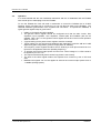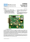
1
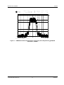
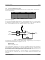
CML Microcircuits
COMMUNICATION SEMICONDUCTORS
UM9980/2 August 2006
EV9980
Evaluation Kit
User Manual
Provisional Issue
Features
• Allows full evaluation and investigation of the
CMX998 Cartesian Feedback Transmitter IC
• Support and interfacing for
customer PAs
• Operational range: 100MHz to 1GHz by use of
on-board matching components
• Interfaces to CMX981 EvKit
• Access to RF, control and baseband signals
via connectors and test points
• Differential or single-ended I and
Q inputs
• Complete demonstration of the CFBL
functionality: default is 400MHz and
configurable for 800MHz
• Can utilise PE0001 EvKit interface
card for PC interface or work with
custom interface equipment
1.
Brief Description
The EV9980 EvKit allows rapid and full evaluation of the CMX998 Cartesian Feedback Transmitter IC.
In the form of a populated PCB, this flexible platform enables users, using a control interface, to configure
and evaluate the CMX998 to various applications and frequency bands.
Access is provided to all CMX998 RF, baseband and control signals by either connector or test points.
Test access points are available to accept common test equipments such as RF and baseband signal
generators and spectrum analysers.
All signal paths are matched by suitable components and the EvKit provides, on-board, two power
amplifier devices, one at 400MHz (default) and one at 800MHz; support is also available for the
connection and operation of a custom PA. The overall operating evaluation frequency range of the EvKit
is for RF frequencies between 100MHz and 1GHz.
The EV9980 can be configured to work with the CMX981 Digital Radio Baseband processor IC or with a
custom baseband system.
No software is required for use of the EvKit; the on-board CMX998 is controlled via its C-BUS serial
interface and control system. An evaluation interface is supplied separately that uses the CML PE0001
EvKit Interface Card and is controlled via the EV9980 PC software. Also a custom C-BUS interface and
control system can be used.
© 2006 CML Microsystems Plc
Evaluation Kit for CMX998
EV9980
CONTENTS
Section
Page
1.
Brief Description ..................................................................................... 1
2.
Preliminary Information.......................................................................... 5
2.1.
Laboratory Equipment.................................................................. 5
2.1.1. Power Supply.................................................................. 5
2.2.
Handling Precautions................................................................... 5
2.2.1. Static Protection.............................................................. 5
2.2.2. Contents - Unpacking ..................................................... 5
2.3.
Approvals ..................................................................................... 5
3.
Quick Start ............................................................................................... 6
3.1.
Setting-Up .................................................................................... 6
3.2.
Input Conditions ........................................................................... 6
3.3.
Operation ..................................................................................... 7
4.
Signal Lists .............................................................................................. 8
5.
Circuit Schematics and Board Layouts.............................................. 12
6.
Detailed Description ............................................................................. 14
6.1.
Hardware Description ................................................................ 14
6.1.1. Cartesian Feedback Loop (CFBL) ................................ 14
6.1.2. Power Amplifiers ........................................................... 14
6.1.3. Local Oscillator (LO) ..................................................... 14
6.1.4. IQ Baseband Inputs ...................................................... 15
6.1.5. CMX981 Interface ......................................................... 15
6.1.6. Manual DC Nulling ........................................................ 15
6.1.7. Power Supply................................................................ 15
6.2.
Adjustments and Controls.......................................................... 15
6.2.1. 800MHz Operation........................................................ 15
6.3.
Software Description.................................................................. 16
6.3.1. The CMX998 ($01-$06) Tab......................................... 16
6.3.2. The CMX998 ($07-$08, $F2-$F8) Tab ......................... 17
6.3.3. The Script Handler Tab................................................. 18
6.4.
Application Information .............................................................. 19
6.4.1. Error Configuration........................................................ 19
6.4.2. Typical Performance of Closed Loop Configuration ..... 20
6.4.3. Testing the CMX998 with the CMX981......................... 25
6.5.
Troubleshooting ......................................................................... 29
6.5.1. Closed Loop Operation ................................................. 29
6.5.2. Open Loop Operation ................................................... 30
7.
Performance Specification................................................................... 31
7.1.
Electrical Performance............................................................... 31
7.1.1. Absolute Maximum Ratings .......................................... 31
7.1.2. Operating Limits............................................................ 31
7.1.3. Operating Characteristics ............................................. 32
© 2006 CML Microsystems Plc
2
UM9980/2
Evaluation Kit for CMX998
EV9980
Table
Page
Table 1 – Signal List......................................................................................................................... 9
Table 2 – PE0001 Interface ............................................................................................................. 9
Table 3 – Test Loops ..................................................................................................................... 10
Table 4 – Test Points ..................................................................................................................... 11
Table 5 – EV9980 and EV9810 interconnection details ................................................................ 25
Table 6 – Closed Loop possible errors .......................................................................................... 29
Table 7 – Open Loop possible errors ............................................................................................ 30
Page
Figure
Figure 1 – Block Diagram ................................................................................................................ 4
Figure 2 – Typical Evaluation Connections for EV9980 .................................................................. 6
Figure 3 – PCB Layout: top............................................................................................................ 12
Figure 4 – PCB Layout: bottom...................................................................................................... 13
Figure 5 – The CMX998 ($01-$06) Tab......................................................................................... 16
Figure 6 – The CMX998 ($07-$08, $F2-$F8) Tab ......................................................................... 17
Figure 7 – The Script Handler Tab ................................................................................................ 18
Figure 8 – Error Amplifier Configuration ........................................................................................ 19
Figure 9 – CMX998 and RF2175 performance closed loop (left) and open loop (right) at
approximately the same PEP output level, 400MHz...................................................................... 20
Figure 10 – CMX998 and RF2175 performance closed loop (lower) and open loop (upper) same
PEP output level with 18ksymbols/s π/4DQPSK modulation, 400MHz ......................................... 20
Figure 11 – CMX998 and RF2175 performance closed loop with 18ksymbols/s π/4DQPSK
modulation, 400MHz ...................................................................................................................... 21
Figure 12 – Broadband (1MHz)plot of CMX998 and RF2175 performance closed loop with
18ksymbols/s π/4DQPSK modulation, 400MHz ............................................................................ 22
Figure 13 – CMX998 and RF2173 performance closed loop (left) and open loop (right) at
approximately the same PEP output level, 800MHz...................................................................... 22
Figure 14 – CMX998 and RF2173 performance closed loop 18dB feedback path attenuation.... 23
Figure 15 – CMX998 and RF2173 performance closed loop with phase control at extremes of
stability = 11.25deg. (left) and 135deg. (right) showing classic peaking of noise when feedback
phase is incorrect. .......................................................................................................................... 23
Figure 16 – CMX998 and RF2173 performance correctly adjusted closed loop with phase control
of 67.50 deg. resulting in a clean spectrum ................................................................................... 24
Figure 17 – CMX998 Input Amplifier Configuration ....................................................................... 25
Figure 18 – CMX998 Configuration for testing with CMX981........................................................ 26
Figure 19 – 1st and 2nd ACP Performance ..................................................................................... 26
Figure 20 – Open and closed loop performance comparison ....................................................... 27
Figure 21 – Trellis Diagram............................................................................................................ 27
Figure 22 – Constellation Diagram ................................................................................................ 28
Figure 23 – Symbol/Error Table..................................................................................................... 28
It is always recommended that you check for the latest product datasheet version from the
Datasheets page of the CML website: [www.cmlmicro.com].
© 2006 CML Microsystems Plc
3
UM9980/2
Evaluation Kit for CMX998
EV9980
LP Filter
External IQ
Inputs
CMX981 Interface
Attenuator
Differential
I/Q
DCMEAS
Instability Detector
PA Ramp
TX-OUT
800MHz
RFOUT
RFIN
CMX998
CFBL
IC
PA
RF2173
Coupler
TX-OUT
400MHz
PA
KEY
C-BUS
Interface
RF2175
Coupler
Interface
Connector
LO-IN
Coax
Connector
Figure 1 – Block Diagram
© 2006 CML Microsystems Plc
4
UM9980/2
Evaluation Kit for CMX998
2.
EV9980
Preliminary Information
The EV9980 provides a platform for the evaluation of the CMX998. To use the EV9980, a
separate micro-controller or PC, for example, is required to program the CMX998 via its C-BUS
interface. This controlling device is not included on the EV9980 but there is a CML product
available to provide the controlling functionality: the PE0001 with EV9980 PC software
(ES9980xx.exe).
2.1.
Laboratory Equipment
The following laboratory equipment is needed to use this evaluation kit:
•
•
•
•
•
Dual Power Supply
Spectrum Analyzer (100MHz to 1GHz)
RF Attenuator
RF Signal Generator (100MHz to 2GHz)
I/Q Signal Source
For more detailed design or investigation work the customer may require other RF test
equipment.
2.1.1.
Power Supply
The supply input voltage to the PCB, for all circuits except the PA, is 7.2V (5.25V to 8V
acceptable). On board regulators are provided to generate all voltage rails used on the PCB (3.3V
and 5V rails are used).
The supply to the PA is directly connected to the PA: a voltage of 3.6V, at the PA, is
recommended. (See also section 6.5.1)
The 7.2V supply should be rated at 1A and the 3.6V supply rated at 2A.
NOTE: Care should be exercised with the supplies, as they are not protected for reverse
polarity. For optimum RF performance, the PA supply is connected directly to the RF2173
and RF2175 device so care is required to ensure the RF2173 and RF2175 manufacturer's
ratings are not exceeded.
2.2.
Handling Precautions
Like most evaluation kits, this product is designed for use in office and laboratory environments.
The following practices will help ensure its proper operation.
2.2.1.
Static Protection
This product uses low power CMOS circuits that can be damaged by electrostatic discharge.
Partially damaged circuits can function erroneously, leading to misleading results. Observe ESD
precautions at all times when handling this product.
2.2.2.
Contents - Unpacking
Please ensure that you have received all of the items on the separate information sheet (EK9980)
and notify CML within 7 working days if the delivery is incomplete.
2.3.
Approvals
This product is not approved to any EMC or other regulatory standard. Users are advised
to observe local statutory requirements, which may apply to this product and the radio
frequency signals that may emanate from it.
© 2006 CML Microsystems Plc
5
UM9980/2
Evaluation Kit for CMX998
3.
EV9980
Quick Start
This section provides instructions for users who wish to experiment immediately with the
evaluation kit. A more complete description of the kit and its use appears later in this document.
The EV9980 includes a CMX998 device that is described in its own, separate, datasheet.
Accordingly, the user should read the current CMX998 datasheet before using the EV9980.
3.1.
Setting-Up
The following procedure is recommended:
1. Connect test leads as shown below in Figure 2.
2. Connect a host µController to C-BUS interface J13 or J15 (alternatively the CML PE0001
card and ES9980xx.exe software can be used – see section 6.3).
3. The power amplifier output (J9) should be connected to a suitable 50Ω load. The default
frequency of operation for the EV9980 is 400MHz.
The use of an external 50Ω Load is essential to prevent possible damage to the PA
stage.
4. Power should be applied to the main supply (7.2V nominal).
5. A connection should be made to J12 pin 15 to allow the PA control volts to be adjusted
6. Power should be applied to the power amplifier supply connector (3.6V).
The board is now ready for operation.
-
-
J3
J2
J13
J15
J11
Baseband IQ
Generator
J7
Pin15
PA Control
Voltage
-
CMX998
J4
-
J8
-
J9
-
J12
J5
J6
J1
-
-
-
J10
30dB RF
Attenuator
RF Spectrum
Analyzer
+7.2V
GND
Power Amp
+3.6V
RF Signal
Generator
Figure 2 – Typical Evaluation Connections for EV9980
3.2.
Input Conditions
LO Input (J1) should be at 800MHz at –10dBm. No baseband I and Q signals (J5 and J3) should
be applied at this time only a 0VDC bias input is required. For reference: the nominal I and Q
input is an AC input signal level of ~500mVp-p at 0VDC bias.
© 2006 CML Microsystems Plc
6
UM9980/2
Evaluation Kit for CMX998
3.3.
EV9980
Operation
It is recommended that the user familiarise themselves with the IC datasheet and the EV9980
user manual prior to attempting to use the EV9980.
To use the EV9980 the user will need a mechanism to control the CMX998 via its C-BUS
interface, which is brought out on connector J13 (J15 can also be used) on the EV9980. The
CMX998 datasheet gives details of the registers and commands. To operate the CMX998, a
typical general register setup is given below:
•
•
•
•
•
•
•
•
•
Initially no IQ signals should be applied.
The general control register should be configured such that the bias circuits, filter
amplifiers, input amplifiers, error amplifiers, forward path and feedback path are all
enabled. Bits 0 and 1 of the general control register should be in their normal operation
state i.e. b0/b1 = 0.
A typical setting for the phase control register would be 22.5degs.
Typical setting for the forward and feedback path attenuator would be 0dB and 13dB
respectively (this configuration gives full output power at 400MHz).
The frequency control register should be set for divide by 2 mode (this means that a LO
input has to be applied at twice the operating frequency).
To achieve the nominal output power from the PA a control voltage of 1.1VDC needs to
be applied to pin 15 of J12.
The output should be analysed to ensure loop phase is set correctly.
The level of the carrier signal needs to be adjusted for a minimum by use of VR1 and
VR2.
Baseband IQ signals can now be applied to achieve the nominal output power level of
~+29dBm (average power).
© 2006 CML Microsystems Plc
7
UM9980/2
Evaluation Kit for CMX998
4.
EV9980
Signal Lists
CONNECTOR PINOUT
Connector
Ref.
Connector
Pin No.
Signal
Name
Signal
Type
J1
N/A
LO-IN
RF
LO input can be applied at 2 x RF output
frequency or 4 x RF output frequency. Nominal
input level is -10dBm.
J2
N/A
TXQ+
Baseband
Q input signal (non-inverting input of input
amplifier)
J3
N/A
TXQ-
Baseband
Q input signal (inverting input of input amplifier)
J4
N/A
RFIN
RF
RF input to feedback path
J5
N/A
TXI-
Baseband
I input signal (inverting input of input amplifier)
J6
N/A
TXI+
Baseband
I input signal (non-inverting input of input
amplifier)
J7
N/A
RFOUT
RF
Upconverter RF output
J8
N/A
TX-OUT
800MHz
RF
800MHz PA output
J9
N/A
TX-OUT
400MHz
RF
400MHz PA output
J10
3
+7.2V
DC
7.2V power supply input
J10
2
+3.6V
DC
3.6V power supply for RF power amplifier
J10
1
GND
DC
Power supply ground
J11
1, 3, 7, 9
TXQ+, TXQTXI-, TXI+
Baseband
Differential I/Q input from the CMX981
evaluation board
J11
2, 4, 5, 6,
8, 10
GNDA
Baseband
Connection to Analogue Ground
J12
1
INSTAB
Baseband
Instability detector output to CMX981 connector
J12
3
DCMEAS
Baseband
DCMEAS output to CMX981 connector
J12
5
FW_Q
Baseband
Forward path baseband Q signal to CMX981
connector
J12
7
FB_Q
Baseband
Feedback path baseband Q signal to CMX981
connector
J12
9
FB_I
Baseband
Feedback path baseband I signal to CMX981
connector
J12
11
FW_I
Baseband
Forward path baseband I signal to CMX981
connector
J12
15
PA_CNTRL
DC
PA control voltage external or from CMX981
evaluation board
© 2006 CML Microsystems Plc
8
Description
UM9980/2
Evaluation Kit for CMX998
EV9980
CONNECTOR PINOUT
Connector
Ref.
Connector
Pin No.
Signal
Name
Signal
Type
J13
1 - 20
C-BUS
Interface
Logic
C-BUS interface from PE0001 or host /
controller PC. See schematics and CMX998
datasheet for details.
J15
1 - 10
Alternative
C-BUS
Interface
Logic
Alternative header for C-BUS interface
Description
Table 1 – Signal List
CONNECTOR PINOUT for J13
Connector
Pin No.
Signal
Name
Signal
Type
Description
1
RESET
I/P
General RESET (RESET active low)
2
CSN
I/P
C-BUS Enable
3
~
~
Spare pin. Leave unconnected.
4
S_DATA_IN
I/P
C-BUS Data Input
5
~
~
Spare pin. Leave unconnected.
6
S_CLOCK
I/P
C-BUS Clock
7
~
~
Spare pin. Leave unconnected.
8
S_DATA_OUT
O/P
C-BUS Data Output
9
~
~
Spare pin. Leave unconnected.
10
IRQN
I/P
Interrupt request - if required. Not used.
11
GNDD
Power
Connection to Digital Ground
12
GNDD
Power
Connection to Digital Ground
13
~
~
Spare pin. Leave unconnected.
14
~
~
Spare pin. Leave unconnected.
15
~
~
Spare pin. Leave unconnected.
16
~
~
Spare pin. Leave unconnected.
17
~
~
Spare pin. Leave unconnected.
18
~
~
Spare pin. Leave unconnected.
19
~
~
Spare pin. Leave unconnected.
20
~
~
Spare pin. Leave unconnected.
Table 2 – PE0001 Interface
© 2006 CML Microsystems Plc
9
UM9980/2
Evaluation Kit for CMX998
EV9980
TEST LOOPS
Test Loop
Ref.
Default
Measurement
Description
TL1
Q Input Amplifier Output
TL2
Instability Detector Output
TL3
Q Image Filter Amplifier Output
TL4
Q Error Amplifier Output
TL5
1.6VDC
BVREF Buffered Vref
TL6
I Error Amplifier Output
TL7
I Image Filter Amplifier Output
TL8
Demodulator Output (Q channel)
TL9
Demodulator Output (I channel)
TL10
I Input Amplifier Output
TL11
Connection point for AVdd on CMX981 evaluation board
TL12
800MHz power amplifier control voltage
TL13
400MHz power amplifier control voltage
TL14
DCMEAS Output
TL15
Spare connection on J12:J13
TL16
C-BUS Data Output
TL17
IRQN (not used)
TL18
GND probe point
TL19
GND probe point
Table 3 – Test Loops
© 2006 CML Microsystems Plc
10
UM9980/2
Evaluation Kit for CMX998
EV9980
TEST POINTS
Test Point
Ref.
Default
Measuremen
t
TP1
3.3V
3.3V regulator output for digital circuits
TP2
3.3V
3.3V regulator output for analogue circuits
TP3
5.0V
5.0V regulator output for RF circuits
TP7
0V
Digital Ground
TP8
0V
Digital Ground
TP9
0V
Analogue Ground
TP10
0V
Analogue Ground
Description
Table 4 – Test Points
Notes:
I/P
O/P
BI
TL
TP
=
=
=
=
=
© 2006 CML Microsystems Plc
Input
Output
Bidirectional
Test Loop
Test Point
11
UM9980/2
Evaluation Kit for CMX998
5.
EV9980
Circuit Schematics and Board Layouts
For clarity, circuit schematics are available as separate high-resolution files. These can be
obtained via the CML website.
The following changes apply to the EV9980 PCB (PCB555B) Mod. State 2, when referring to
schematic (DWG9980B04.pdf). These changes have already been made to the Evaluation Kit.
No
1
Circuit Area and
Component Reference
+V power line
C109, C133, J10
Comment
Change
Cure coupling between
400MHz PA and power
supply which caused
degraded adjacent
channel power.
Cut +V track on the top layer of
the board close to C109
Place a wire link on bottom
layer between J10 pin 3 and
C133
The layout on each side of the pcb is shown in Figure 3 and Figure 4, below:
Figure 3 – PCB Layout: top
© 2006 CML Microsystems Plc
12
UM9980/2
Evaluation Kit for CMX998
EV9980
Figure 4 – PCB Layout: bottom
© 2006 CML Microsystems Plc
13
UM9980/2
Evaluation Kit for CMX998
6.
EV9980
Detailed Description
The CMX998 datasheet (not included, but available at www.cmlmicro.com) should be referred to
for a detailed description of the CMX998 device.
The EV9980 functionality includes:
•
•
•
•
•
Demonstration of the CFBL RF functionality, PA devices have been included to allow
operation at 400MHz and 800MHz to be evaluated in detail.
Operation at 100MHz to 1000MHz.
Support for customer power amplifiers at different powers and frequencies over the full
operating range of the CFBL IC.
C-BUS Interface that allows the card to be connected to a host µController. Interface to a PC
for initial test and customer evaluation is available separately with suitable PC software that
allows control of all device functions.
Interface directly to CMX981 evaluation card allows demonstration of:
o
o
π/4-DQPSK modulation
burst and continuous transmission
In summary, the EV9980 allows the user to create experiments to investigate all aspects of the
CMX998 device. The EV9980 is designed to allow user modification, to support detailed
investigation of each user’s specific and different applications.
6.1.
Hardware Description
6.1.1.
Cartesian Feedback Loop (CFBL)
The card is configured to allow the CFBL to operate in normal operation with single ended
external inputs. The gains are set in the baseband amplifier sections to suit the input drive levels
in section 6.1.4. The error amplifier is configured with a loop filter optimised for operation with the
on-board power amplifiers but can be configured with user values for any other requirements. It is
possible to access the up-converter output and the down-converter input so that customers can
connect their own power amplifiers into the loop. The LO input, up-converter output and the
down-converter input are all matched with broadband balun/transformer to allow wideband
operation from 100MHz to 1GHz.
The RESET pin (active low) is pulled high with 100k ohms. The user can pull this pin low to reset
the device (or the software reset can be used).
6.1.2.
Power Amplifiers
The card includes power amplifiers to demonstrate the CFBL IC at ~400MHz or ~800MHz. The
400MHz amplifier (default connection) is capable of producing 29~30dBm (mean) with pulsed π/4DQPSK modulation. An option of using a 800MHz power amplifier is included in the design and
this is also capable of 30dBm (mean) output with π/4-DQPSK modulation. Component changes
are required to make use of this option, see section 6.2.1.
Gain control has been included which allows the power amplifiers to be connected to the CMX981
Ramping DAC or to an external variable voltage source.
6.1.3.
Local Oscillator (LO)
The local oscillator has not been provided on the EV9980. A connector is provided to allow an
external oscillator source to be injected at twice or four times the RF output frequency depending
on the oscillator mode selected.
© 2006 CML Microsystems Plc
14
UM9980/2
Evaluation Kit for CMX998
6.1.4.
EV9980
IQ Baseband Inputs
The board allows the IQ inputs to come from the CMX981 or from an alternative external source.
The input can be differential or single ended. Adjusting the values around the CMX998 input
amplifiers creates the required input configuration. The default setup is for single ended inputs,
which are applied to TXI- and TXQ-. A typical input signal would be ~500mVp-p at 0VDC bias.
6.1.5.
CMX981 Interface
The EV9980 has an interface to allow connection to the CMX981 Evaluation card. There are two
connectors J11 and J12 that include the following signals:
•
•
•
•
•
6.1.6.
I/Q Input signals from CMX981
DCMEAS pin from CMX998 to CMX981 AUX ADC
Ramping DAC signal from CMX981 to EV9980 power amplifiers
Instability detector output
DC Nulling signal input (optional)
Manual DC Nulling
The DC nulling can be done manually through the use of VR1 and VR2 variable resistors. They
affect the DC level of at the input to the modulator so that the carrier can be nulled to a minimum
manually. Automatic control has been implemented through the CMX981 interface.
6.1.7.
Power Supply
The input to the PCB for CMX998 and interface circuits is nominally 7.2V (5.25V to 8V is
acceptable). On board regulators are provided to generate voltage rails used on the EV9980
(3.3V used for CFBL IC).
The power supply to the PA is directly from a separate 3.6V input.
6.2.
Adjustments and Controls
The user has the ability to configure the EV9980 for a number of different operational scenarios.
6.2.1.
800MHz Operation
The default operating frequency is 400MHz, so the following components need to be changed to
enable the EV9980 to work at 800MHz:
•
•
•
•
•
C98, C99, R86 become not fitted (NF)
C76, C78 should be 1nF
R74 should be 0R
L10 should be 0R
C121, C122 should be not fitted (NF)
Typical values for CMX998 registers at 800MHz are:
•
•
•
phase control register 67.50 degrees
forward path attenuation = 0dB
feedback path attenuation = 18dB
(Note: for 400MHz typical values see section 3.3)
© 2006 CML Microsystems Plc
15
UM9980/2
Evaluation Kit for CMX998
6.3.
EV9980
Software Description
The EV9980 does not require any embedded firmware. The CML product PE0001, available
separately, can be used with the EV9980 and the related PC software (ES9980xx.exe). The
ES9980 application allows the user to interact with the EV9980 via an easy to use graphical
interface. It consists of three tabs: each one representing a particular set of registers or a
particular function of the CMX998.
To select a tab simply click on the corresponding name in the row at the top of the program
window. Setting or clearing the check box associated with a bit of a register will cause that bit to
be set or cleared when the register is next written to. If the ‘Auto Write’ check box is set a register
will be written whenever a check box or list box associated with it is modified. This removes the
need to click the ‘Write’ button associated with that register. The program can be closed at any
time by clicking the ‘Close’ button or by pressing ‘Alt’ and ‘C’ keys simultaneously.
6.3.1.
The CMX998 ($01-$06) Tab
The CMX998 ($01-$06) tab gives access to the general control register, gain control register,
phase control register and general reset command, see Figure 5.
In the case of the gain and phase control register slide bars have been used to allow easy control
during operation.
Figure 5 – The CMX998 ($01-$06) Tab
© 2006 CML Microsystems Plc
16
UM9980/2
Evaluation Kit for CMX998
6.3.2.
EV9980
The CMX998 ($07-$08, $F2-$F8) Tab
The CMX998 ($07-$08, $F2-$F8) tab gives access to the aux control and frequency control
registers, see Figure 6. This tab also allows the registers $F2 to $F8 to be read individually.
Figure 6 – The CMX998 ($07-$08, $F2-$F8) Tab
© 2006 CML Microsystems Plc
17
UM9980/2
Evaluation Kit for CMX998
6.3.3.
EV9980
The Script Handler Tab
The Script Handler tab allows the execution of script files consisting of register write and read,
delay commands, see Figure 7.
Figure 7 – The Script Handler Tab
The script files should be ASCII text files with each line containing one of following commands:
•
•
•
•
•
•
Register write (8 bit) –
Register read (8 bit) –
Register write (16 bit) –
Register read (16 bit) –
Delay Comment line -
WR8_AA_DD
RD8_AA
W16_AA_DDDD
R16_AA
DELAY_X..X
//C..C
Where AA is the 2 digit register address in hexadecimal, _ is a single space character, DD is the
2 digit register value in hexadecimal, X..X is a time to delay by in 10ms units and C..C is an
ASCII string. The delay command stops any following script commands from being executed until
the delay period has passed.
© 2006 CML Microsystems Plc
18
UM9980/2
Evaluation Kit for CMX998
EV9980
Each line must contain only one command and no other characters. An example script file is:
// Example Script File for EV9980
//
//
WR8 01 00
// send RESET
//
WR8 02 3F
//ENABLE VBIAS, Filter Pwr, Input Amp Pwr, Error Amp PWR, Open
Loop Mode, Error Amp Gain reduction
//
RD8 F2
// Read General Control Register
//
w16 04 0012
R16 F4
// Set Forward gain=0dB, Feedback gain=-20dB; Read back Gain
Control Register
The results window will display the value returned by register read commands. These results can
be saved to an ASCII text file or discarded by clicking on the ‘Save Results’ or ‘Clear Results’
buttons, respectively.
The ES9980 application will update the displayed register values to reflect those of any register
read or write commands contained in an executed script file. When script file is being executed
the other tabs cannot be selected. A script file can be executed once, repeatedly until the ‘Stop’
button is pressed or a specified number of times. The execution of a script file can be stopped or
paused at any time by clicking the appropriate button.
6.4.
Application Information
6.4.1.
Error Configuration
The error amplifier configuration used on the EV9980 is shown in Figure 8. The following
conditions apply to the values fitted on the EV9980, the 1st Pole is at ~16kHz, the 2nd Pole is at
~32kHz and the Zero is at ~320kHz. These can be changed for any user requirement.
C21/
C41
R18/R38
FW_I/Q
R25/R32
R20/R36
MODIP/
MODQP
Error Amp
FB_I/Q
C26/
C36
R21/R37
R24/
R40
C24/C37
Figure 8 – Error Amplifier Configuration
© 2006 CML Microsystems Plc
19
UM9980/2
Evaluation Kit for CMX998
6.4.2.
EV9980
Typical Performance of Closed Loop Configuration
The following plots show typical performance of the EV9980 with two-tone and 18ksymbols/s
π/4DQPSK modulation.
Delta 3 [T1]
Ref Lvl
-63.23 dB
44 dBm
RBW
500 Hz
VBW
500 Hz
SWT
-32.06412826 kHz
RF Att
40 dB
Delta 3 [T1]
Ref Lvl
2 s
Unit
dBm
44
RBW
500 Hz
VBW
500 Hz
SWT
-32.06412826 kHz
RF Att
2 s
40 dB
Unit
dBm
44
30.5 dB Offset
40
-27.70 dB
44 dBm
1 [T1]
26.17 dBm
A
30.5 dB Offset
40
1 [T1]
400.00911824 MHz
3 [T1]
30
1
3 [T1]
-32.06412826 kHz
1
1 [T1]
20
-32.37 dB
-9.01803607 kHz
-62.15 dB
16.03206413 kHz
10 1VIEW
-27.70 dB
30
-39.97 dB
-9.01803607 kHz
2 [T1]
A
400.00911824 MHz
-63.23 dB
-32.06412826 kHz
1 [T1]
20
25.59 dBm
2 [T1]
1SA
16.03206413 kHz
10 1VIEW
0
0
-10
-10
-29.48 dB
3
1SA
2
1
1
-20
-20
-30
-30
2
3
-40
-40
-50
-50
-56
-56
Center 400 MHz
Date:
10 kHz/
10.MAR.2006
Span 100 kHz
Center 400 MHz
09:30:22
Date:
10 kHz/
10.MAR.2006
Span 100 kHz
09:30:53
Figure 9 – CMX998 and RF2175 performance closed loop (left) and open loop (right) at
approximately the same PEP output level, 400MHz
RBW
500 Hz
Ref Lvl
VBW
500 Hz
35 dBm
SWT
2 s
RF Att
Unit
30 dB
dBm
35
30.5 dB Offset
A
30
20
10
1VIEW
2VIEW
0
1SA
2SA
-10
-20
-30
-40
-50
-60
-65
Center 400 MHz
Date:
10.MAR.2006
10 kHz/
Span 100 kHz
09:38:51
Figure 10 – CMX998 and RF2175 performance closed loop (lower) and open loop (upper) same
PEP output level with 18ksymbols/s π/4DQPSK modulation, 400MHz
© 2006 CML Microsystems Plc
20
UM9980/2
Evaluation Kit for CMX998
EV9980
Marker 1 [T1]
RBW
500 Hz
Ref Lvl
19.44 dBm
VBW
500 Hz
35 dBm
400.00330661 MHz
SWT
2 s
RF Att
Unit
30 dB
dBm
35
30.5 dB Offset
1 [T1]
19.44 dBm
30
A
400.00330661 MHz
CH PWR
1
20
28.73 dBm
ACP Up
-66.60 dB
ACP Low
-64.87 dB
1 [T1]
0.00 dB
10
0.00000000 Hz
1VIEW
0
1SA
-10
-20
-30
-40
C0
C0
-50
cl1
cl1
cu1
-60
cu1
-65
Center 400 MHz
Date:
10.MAR.2006
10 kHz/
Span 100 kHz
09:35:15
Figure 11 – CMX998 and RF2175 performance closed loop with 18ksymbols/s π/4DQPSK
modulation, 400MHz
© 2006 CML Microsystems Plc
21
UM9980/2
Evaluation Kit for CMX998
EV9980
RBW
5 kHz
Ref Lvl
VBW
5 kHz
35 dBm
SWT
RF Att
100 ms
30 dB
Unit
dBm
35
30.5 dB Offset
A
30
20
10
0
2VIEW
2SA
-10
-20
-30
-40
-50
-60
-65
Center 400 MHz
Date:
100 kHz/
10.MAR.2006
Span 1 MHz
09:40:39
Figure 12 – Broadband (1MHz)plot of CMX998 and RF2175 performance closed loop with
18ksymbols/s π/4DQPSK modulation, 400MHz
Marker 1 [T1]
RBW
500 Hz
Ref Lvl
27.84 dBm
VBW
500 Hz
35 dBm
799.99328657 MHz
SWT
2 s
RF Att
Unit
RBW
500 Hz
Ref Lvl
27.44 dBm
VBW
500 Hz
35 dBm
799.99328657 MHz
SWT
Marker 1 [T1]
30 dB
dBm
2 s
RF Att
Unit
30 dB
dBm
35
35
30.5 dB Offset
1 [T1]
1
30
30.5 dB Offset
27.84 dBm
30
A
1 [T1]
1
799.99328657 MHz
1 [T1]
2 [T1]
1 [T1]
20
2 [T1]
-55.87 dB
3 [T1]
-16.03206413 kHz
4 [T1]
0
0
1
-32.06412826 kHz
1
-10
-27.61 dB
-16.03206413 kHz
3
-58.31 dB 1SA
-31.24 dB
7.01402806 kHz
10
3 [T1]
-32.20 dB
-2.00400802 kHz
-40.64 dB
7.01402806 kHz
10
A
799.99328657 MHz
-39.49 dB
-2.00400802 kHz
20
27.44 dBm
2
4 [T1]
-37.45 dB
1SA
-32.06412826 kHz
4
-10
2
-20
-20
3
4
-30
-30
-40
-40
-50
-50
-60
-60
-65
-65
Center 800 MHz
Date:
10.MAR.2006
10 kHz/
15:06:24
Center 800 MHz
Span 100 kHz
Date:
10.MAR.2006
10 kHz/
Span 100 kHz
15:08:04
Figure 13 – CMX998 and RF2173 performance closed loop (left) and open loop (right) at
approximately the same PEP output level, 800MHz
© 2006 CML Microsystems Plc
22
UM9980/2
Evaluation Kit for CMX998
EV9980
RBW
500 Hz
Ref Lvl
26.45 dBm
VBW
500 Hz
35 dBm
799.99328657 MHz
SWT
Marker 1 [T1]
RF Att
2 s
30 dB
Unit
dBm
35
30.5 dB Offset
1 [T1]
30
1
26.45 dBm
A
799.99328657 MHz
1 [T1]
-39.63 dB
20
-2.00400802 kHz
2 [T1]
-45.63 dB
7.01402806 kHz
10
3 [T1]
-65.19 dB
-16.03206413 kHz
0
4 [T1]
-66.88 dB
1SA
-32.06412826 kHz
-10
1
2
-20
-30
3
4
-40
-50
-60
-65
Center 800 MHz
Date:
10 kHz/
10.MAR.2006
Span 100 kHz
15:07:21
Figure 14 – CMX998 and RF2173 performance closed loop 18dB feedback path attenuation
RBW
5 kHz
Ref Lvl
VBW
5 kHz
35 dBm
SWT
100 ms
RF Att
Unit
RBW
5 kHz
Ref Lvl
VBW
5 kHz
35 dBm
SWT
30 dB
dBm
100 ms
RF Att
Unit
30 dB
dBm
35
35
30.5 dB Offset
30.5 dB Offset
A
30
A
30
20
20
10
10
0
0
2SA
2SA
-10
-10
-20
-20
-30
-30
-40
-40
-50
-50
-60
-60
-65
-65
Center 800 MHz
Date:
10.MAR.2006
100 kHz/
15:11:11
Center 800 MHz
Span 1 MHz
Date:
10.MAR.2006
100 kHz/
Span 1 MHz
15:10:46
Figure 15 – CMX998 and RF2173 performance closed loop with phase control at extremes of
stability = 11.25deg. (left) and 135deg. (right) showing classic peaking of noise when feedback
phase is incorrect.
© 2006 CML Microsystems Plc
23
UM9980/2
Evaluation Kit for CMX998
EV9980
RBW
5 kHz
Ref Lvl
VBW
5 kHz
35 dBm
SWT
100 ms
RF Att
Unit
30 dB
dBm
35
30.5 dB Offset
A
30
20
10
0
2SA
-10
-20
-30
-40
-50
-60
-65
Center 800 MHz
Date:
10.MAR.2006
100 kHz/
Span 1 MHz
15:10:17
Figure 16 – CMX998 and RF2173 performance correctly adjusted closed loop with phase control of
67.50 deg. resulting in a clean spectrum
© 2006 CML Microsystems Plc
24
UM9980/2
Evaluation Kit for CMX998
6.4.3.
EV9980
Testing the CMX998 with the CMX981
The EV9980 has an IQ interface to the EV9810 through the use of a 10-way header. The connections
should be made, as follows:
EV9980 (J11)
Label
Pin No
981_Q+
1
981_Q3
GNDA
5
981_I7
981_I+
9
EV9810 (J9)
Label
Pin No
QTXP
10
QTXN
8
GNDANALOG
6
ITXN
4
ITXP
2
Table 5 – EV9980 and EV9810 interconnection details
(Note: See also Figure 18).
The TX output of the CMX981 is differential I and Q, with a single ended signal level of 1Vp-p @1.28VDC.
The CMX998 input amplifiers need to convert this differential signal into a single ended 1Vp-p @1.6VDC
signal. A typical configuration for the input amplifiers on the 998 is shown in Figure 17.
+3.3V
620k
100k
1Vp-p
@1.28VDC
1Vp-p
@1.28VDC
Input Amp
100k
1Vp-p
@1.6VDC
10k
Figure 17 – CMX998 Input Amplifier Configuration
The results shown in this section were taken with the CMX998 configured as Figure 18. The component
changes to the EV9980 to allow this configuration to work are:
Move C55 to C54
Move C27 to C30
Make C35 a 0R (0603 resistor)
To get ~0dBm after the splitter (splitter loss assumed to be ~3dB) the attenuator in the forward path =
0dB, the attenuator in the feedback path ~23-24dB. The optimal phase setting will vary between setups
as it is determined by the length of leads used to complete the RF loop. On a 1MHz span on the
spectrum analyser, check for noise humping to ensure correct phase has been set.
The plots in Figure 19, Figure 20, Figure 21, Figure 22 and Figure 23 show the ACP performance, an
open and closed loop comparison, trellis diagram, constellation diagram and symbol/error table
respectively.
© 2006 CML Microsystems Plc
25
UM9980/2
Evaluation Kit for CMX998
EV9980
EV9980
1
-
-
J3
J2
J13
J9
J15
EV9810
J11
1
Splitter
CMX998
J7
J4
-
J8
-
J9
-
J12
J5
J6
J1
-
-
-
RF Spectrum
Analyzer-
J10
+7.2V
GND
Do Not Connect
a supply to
+V_PA
RF Signal
Generator
Figure 18 – CMX998 Configuration for testing with CMX981
Marker 1 [T1]
-19.84 dBm
Ref Lvl
389.99780261 MHz
0 dBm
RBW
500 Hz
VBW
2 kHz
SWT
RF Att
2.4 s
0
30 dB
Unit
1 [T1]
dBm
-19.84 dBm
389.99780261 MHz
CH PWR
-10
A
0.14 dBm
ACP Up
-69.05 dB
ACP Low
-70.33 dB
1
-20
ALT1 Up
-74.52 dB
ALT1 Low
-73.71 dB
-30
1SA
-40
-50
-60
cl2
-70
cl2
cu2
cu2
-80
C0
C0
cl1
cl1
-90
cu1
cu1
-100
Center 390 MHz
Date:
15.MAR.2006
11.8 kHz/
Span 118 kHz
09:54:45
Figure 19 – 1st and 2nd ACP Performance
© 2006 CML Microsystems Plc
26
UM9980/2
Evaluation Kit for CMX998
EV9980
Marker 1 [T1]
Ref Lvl
-21.56 dBm
0 dBm
RBW
500 Hz
VBW
2 kHz
SWT
RF Att
2.4 s
30 dB
Unit
dBm
389.99780261 MHz
0
1 [T1]
-21.56 dBm
A
389.99780261 MHz
-10
CH PWR
-20
1
-30
0.30 dBm
ACP Up
-68.56 dB
ACP Low
-69.60 dB
ALT1 Up
-75.74 dB
ALT1 Low
-75.45 dB
1VIEW
1SA
2SA
-40
-50
-60
-70
cl2
cl2
cu2
-80
cu2
C0
C0
cl1
-90
cl1
cu1
cu1
-100
Center 390 MHz
Date:
15.MAR.2006
11.8 kHz/
Span 118 kHz
09:56:29
Figure 20 – Open and closed loop performance comparison
Ref Lvl
5 dBm
CF
390 MHz
SR
18 kHz
Meas Signal
Trellis
Standard
TETRA
450
A
PHASE
Þ
T1
BURST NOT FOUND
-450
0
Date:
SYMBOLS
15.MAR.2006
4
10:01:36
Figure 21 – Trellis Diagram
© 2006 CML Microsystems Plc
27
UM9980/2
Evaluation Kit for CMX998
EV9980
Ref Lvl
5 dBm
CF
390 MHz
SR
18 kHz
Meas Signal
Constellation
Standard
TETRA
1.5
A
IMAG
T1
BURST NOT FOUND
-1.5
-1.875
Date:
REAL
15.MAR.2006
1.875
10:37:30
Figure 22 – Constellation Diagram
Ref Lvl
5 dBm
CF
390 MHz
SR
18 kHz
Symbol/Errors
Standard
TETRA
Symbol Table
A
0
11111001 10010011 00000100 01110100 10111011
40
01110010 10010101 01011011 11010111 01011010
80
00111001 10000111 10111110 01000110 01110100
120
11010011 10110010 00000111 11110110 11000110
160
11100110 11101000 10111110 10101110 01001011
200
00100010 11001111 11110111 01100101 11101011
240
11110010 00000100 01100000 11010111 01010011
280
10001111 10010011 10011011 00101001 10101001
320
11100110 00000000 10000001 01011111 00110110
360
11010010 01011100 11011010 01110001 00000111
400
00101100 01111101 01111000 01111010 00001111
440
11100011 11011111 11011001 00111101 10101101
480
00000111 1000
Error Summary
BURST NOT FOUND
Error Vector Mag
3.62 % rms
6.81 %
Pk at sym
Magnitude Error
2.64 % rms
-6.02 %
Pk at sym
6
Phase Error
1.42 deg rms
2.97 deg Pk at sym
205
Freq Error
-3.50
Hz
-3.50
8
Hz Pk
Amplitude Droop
0.79 dB/sym
Rho Factor
0.9977
IQ Offset
3.48 %
IQ Imbalance
0.54 %
Date:
15.MAR.2006
10:36:58
Figure 23 – Symbol/Error Table
© 2006 CML Microsystems Plc
28
UM9980/2
Evaluation Kit for CMX998
6.5.
EV9980
Troubleshooting
The CMX998 is a complex RF system. If incorrectly programmed or modified, results will be at
variance from datasheet performance. Please study the IC datasheet, this manual and the
associated schematics and layout drawings carefully when troubleshooting.
This section provides some suggestions to help users resolve application issues they might
encounter.
6.5.1.
Closed Loop Operation
Error Observed
Possible Cause
Remedy
Instability, poor adjacent channel
performance
Loop Phase is incorrect
Try adjusting the phase control
register while analysing the RF
output to see if spectrum
improves
PA supply draws more 1.5A
Loop Phase incorrect
See above remedy above.
No RF Output
PA control volts are low, relevant
circuitry not enable, or IQ signals
not applied.
Check control volts at TL13 (or
TL12) to see if voltage is close to
+2.8VDC, try re-enabling circuitry
in CMX998 or measure IQ signal
at TL1.
No linearization of PA appears to
be happening
Loop switch in wrong position,
forward/reverse attenuator
incorrectly set
Check state of loop switch, and
adjust attenuator to see if
spectrum improves.
No linearization of PA appears to
be happening
Error amp gain reduction mode
has been selected
Discrete spurious present on
transmission at 18kHz offset from
carrier causing degrading
adjacent channel power when
using EV9810 to generate
modulation.
Insufficient issoluation between
EV9980 and EV9810 power
supplies
Ensure sufficient de-coupling
between power supplies or use
separate bench power supplies
for EV9810 and EV9980.
RF output from 400MHz PA is
low (e.g. +27dBm mean)
Voltage drop in wires to PA
results in a low supply voltage
Measure the PA supply voltage
at the PA pin. Increase supply
voltage so that at least 3.6V is
seen at the pin. NB: Do not
exceed manufactures absolute
maximum value when the PA is
not transmitting.
Table 6 – Closed Loop possible errors
© 2006 CML Microsystems Plc
29
UM9980/2
Evaluation Kit for CMX998
6.5.2.
EV9980
Open Loop Operation
Error Observed
No RF Output
Possible Cause
Relevant circuitry not enable, or
IQ signals not applied.
Remedy
Try re-enabling circuitry in
CMX998 or measure IQ signal at
TL1.
Table 7 – Open Loop possible errors
© 2006 CML Microsystems Plc
30
UM9980/2
Evaluation Kit for CMX998
7.
Performance Specification
7.1.
Electrical Performance
7.1.1.
Absolute Maximum Ratings
EV9980
Exceeding these maximum ratings can result in damage to the Evaluation Kit.
Min.
0
0
0
-20
Supply Voltage (VIN - VSS)
Supply Voltage (VPA - VSS)
Current into or out of VIN, VPA and VSS pins
Current into or out of any other connector pin
7.1.2.
Max.
8.0
4.0
+2.0
+20
Units
V
V
A
mA
Max.
8.0
3.6
Units
V
V
Operating Limits
Correct operation of the Evaluation Kit outside these limits is not implied.
Notes
Supply Voltage (VIN - VSS)
Supply Voltage (VPA - VSS)
Notes:
1.
1
Min.
5.25
3.0
PA supply voltage should be measured at the Power Amplifier (U2 or U5) power supply
pin.
© 2006 CML Microsystems Plc
31
UM9980/2
Evaluation Kit for CMX998
7.1.3.
EV9980
Operating Characteristics
For the following conditions unless otherwise specified:
VIN - VSS = 7.2V, VPA - VSS = 3.6V, Tamb = +25°C.
Notes
Min.
Typ.
Max.
Units
2
2
–
–
4
135
–
–
mA
mA
Up-Converter Output
Output power
Attenuator Range
Atenuator Step Size
–
0
–
0
–
2.5
–
30
–
dBm
dB
dB
Down-Converter Input
Input impedance
Input Level
Attenuator Range
Attenuator Step Size
–
-22
0
–
50
–
–
1.0
–
+7
29
–
Ω
dBm
dB
dB
IQ Input Signal
Amplitude
DC Level
–
–
0.5
0
–
–
Vp-p
VDC
LO Input
Input impedance
Frequency range
Input Level
–
200
-10
50
–
–
–
2000
-5
Ω
MHz
dBm
–
390
50
400
+32
-60
–
410
Ω
MHz
dBm
dBc
–
50
800
+33
–
Ω
MHz
dBm
DC Parameters (Excluding PA Supply)
IDD (CMX998 powersaved)
IDD (All CMX998 Circuitry Enabled)
AC Parameters
400MHz PA Output
Input impedance
Frequency range
Output Level (PEP)
Adjacent Channel Power
3
4
800MHz PA Output
Input impedance
Frequency range
Output Level (PEP)
C-BUS Interface
See CMX998 Datasheet
Notes:
2.
3.
4.
PCB current consumption, not current consumption of the CMX998.
+32dBm is generally achieved with continious operation, +33dBm can be achieved using
burst transmission typical in TDMA systems
Using TETRA π/4-DQPSK modulation at 18ks/s, 18kHz measurement bandwidth for
adjacent channel power.
© 2006 CML Microsystems Plc
32
UM9980/2
Evaluation Kit for CMX998
7.1.3
EV9980
Operating Characteristics - Timing Diagrams
Please refer to CMX998 Datasheet for details.
CML does not assume any responsibility for the use of any circuitry described. No IPR or circuit patent licences are
implied. CML reserves the right at any time without notice to change the said circuitry and any part of this product
specification. Evaluation kits and demonstration boards are supplied for the sole purpose of demonstrating the
operation of CML products and are supplied without warranty. They are intended for use in a laboratory environment
only and are not for re-sale, end-use or incorporation into other equipments. Operation of these kits and boards outside
a laboratory environment is not permitted within the European Community. All software/firmware is supplied "as is" and
is without warranty. It forms part of the product supplied and is licensed for use only with this product, for the purpose of
demonstrating the operation of CML products. Whilst all reasonable efforts are made to ensure that software/firmware
contained in this product is virus free, CML accepts no resonsibility whatsoever for any contamination which results from
using this product and the onus for checking that the software/firmware is virus free is placed on the purchaser of this
evaluation kit or development board.
www.cmlmicro.com
For FAQs see: www.cmlmicro.com/products/faqs/
For a full datasheet listing see: www.cmlmicro.com/products/datasheets/download.htm
For detailed application notes: www.cmlmicro.com/products/applications/
CML Microcircuits
(UK ) Ltd
CML Microcircuits
(USA) Inc.
CML Microcircuits
(Singapore) Pte Ltd
COMMUNICATION SEMICONDUCTORS
COMMUNICATION SEMICONDUCTORS
COMMUNICATION SEMICONDUCTORS
Oval Park, Langford,
Maldon, Essex,
CM9 6WG - England.
4800 Bethania Station Road,
Winston-Salem,
NC 27105 - USA.
No 2 Kallang Pudding Road,
#09 - 05/06 Mactech
Industrial Building,
Singapore 349307
No. 218, Tian Mu Road
West, Tower 1, Unit 1008,
Shanghai Kerry Everbright
City, Zhabei,
Shanghai 200070,
China.
Tel: +44 (0)1621 875500
Tel: +65 6745 0426
Fax: +44 (0)1621 875600
Tel: +1 336 744 5050,
800 638 5577
Fax: +1 336 744 5054
Fax: +65 6745 2917
Tel: +86 21 6317 4107
+86 21 6317 8916
Fax: +86 21 6317 0243
Sales:
[email protected]
Sales:
[email protected]
Sales:
[email protected]
Sales:
[email protected]
Technical Support:
[email protected]
Technical Support:
[email protected]
Technical Support:
[email protected]
Technical Support:
[email protected]