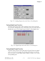
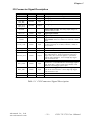
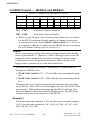
1
Copyright
This documentation and the software included with this product are
copyrighted 1999 by Advantech Co., Ltd. All rights are reserved.
Advantech Co., Ltd. reserves the right to make improvements in the
products described in this manual at any time without notice.
No part of this manual may be reproduced, copied, translated or
transmitted in any form or by any means without the prior written
permission of Advantech Co., Ltd. Information provided in this
manual is intended to be accurate and reliable. However, Advantech
Co., Ltd. assumes no responsibility for its use, nor for any infringements of the rights of third parties which may result from its use.
Acknowledgments
PC-LabCard is a trademark of Advantech Co., Ltd. IBM and PC are
trademarks of International Business Machines Corporation. MSDOS, Windows, Microsoft Visual C++ and Visual BASIC are trademarks of Microsoft Corporation. Intel and Pentium are trademarks of
Intel Corporation. Delphi and C++Builder are trademarks of Inprise
Corporation.
CE notification
The PCI-1711/1731, developed by ADVANTECH CO., LTD., has
passed the CE test for environmental specifications when shielded
cables are used for external wiring. We recommend the use of
shielded cables. This kind of cable is available from Advantech.
Please contact your local supplier for ordering information.
On-line Technical Support
For technical support and service, please visit our support website at:
http://support.advantech.com
Part No. 2003171100
Printed in Taiwan
1st Edition
October 1999
Contents
1. Introduction .................................................. 1
1.1 Features ............................................................................... 1
1.2 Installation Guide ................................................................ 3
1.3 Software ............................................................................... 5
1.4 Accessories .......................................................................... 5
2. Installation ..................................................... 7
2.1 Unpacking ............................................................................ 7
2.2 Driver Installation ................................................................ 8
2.3 Hardware Installation .......................................................... 9
2.4 Device Setup & Configuration .......................................... 12
2.5 Device Testing ................................................................... 15
3. Signal Connections ................................... 19
3.1 Overview ............................................................................ 19
3.2 I/O Connector ..................................................................... 19
3.3 Analog Input Connections ................................................ 22
3.4 Analog Output Connections .............................................. 22
3.5 Trigger Source Connections ............................................. 23
3.6 Field Wiring Considerations ............................................. 24
4. Software Overview ..................................... 25
4.1 Programming Choices ...................................................... 25
4.2 DLL Driver Programming Roadmap ................................ 27
5. Calibration ................................................... 29
5.1 VR Assignment ................................................................... 29
5.2 A/D Calibration .................................................................. 30
5.3 D/A Calibration .................................................................. 30
5.4 Self A/D Calibration ........................................................... 31
Appendix A
Specifications ................................................. 33
Appendix B
Block Diagram ................................................ 35
Appendix C
Register Structure and Format .................... 37
C.1 Overview ............................................................................ 37
C.2 I/O Port Address Map ........................................................ 37
C.3 Channel Number and A/D Data — BASE+0 and
BASE+1 .............................................................................. 42
C.4 Software A/D Trigger — BASE+0 .................................... 42
C.5 A/D Channel Range Setting — BASE+2 ......................... 43
C.6 MUX Control — BASE+4 and BASE+5 ............................ 44
C.7 Status Register — BASE+6 and BASE+7 ......................... 45
C.8 Control Register — BASE+6 ............................................. 46
C.9 Clear Interrupt and FIFO — BASE+8 and BASE+9 ......... 47
C.10 D/A Output Channel 0 — BASE+10 and BASE+11 ......... 47
C.11 D/A Output Channel 1 — BASE+12 and BASE+13 ......... 48
C.12 D/A Reference Control —BASE+14 ................................ 49
C.13 Digital I/O Registers — BASE+16 and BASE+17 ............ 50
C.14 Programmable Timer/Counter Registers BASE+24,
BASE+26, BASE+28 and BASE+30 ................................. 50
Appendix D
82C54 Counter Function ............................... 51
D.1 The Intel 82C54 .................................................................. 51
D.2 Counter Read/Write and Control Registers ..................... 51
D.3 Counter Operating Modes ................................................ 53
D.4 Counter Operations ........................................................... 55
1
Chapter 1
Chapter
1. Introduction
Thank you for buying the Advantech PCI-1711/1731 PCI card. The
Advantech PCI-1711/1731 is a powerful data acquisition (DAS) card for
the PCI bus. It features a unique circuit design and complete functions
for data acquisition and control. PCI-1711/1731 provides specific
functions for different user requirements:
PCI-1711 12-bit Low-cost Multifunction DAS card
PCI-1731 12-bit Low-cost Multifunction DAS card w/o analog output
The following sections of this chapter will provide further information
about features of the DAS cards, a Quick Start for installation, together
with some brief information on software and accessories for the PCI1711/1731 card.
1.1 Features
The Advantech PCI-1711/1731 provides users with the most requested
measurement and control functions as seen below:
q 16-channel Single-Ended A/D Input
q 12-bit A/D conversion with up to 100 kHz sampling rate
q 16-channel Digital Input
q 16-channel Digital Output
q 2-channel D/A Output (only for PCI-1711)
q Programmable Counter/Timer
q Automatic Channel/Gain Scanning
The Advantech PCI-1711/1731 offers the following main features:
Plug-and-Play Function
The Advantech PCI-1711/1731 is a Plug-and-Play device, which fully
complies with the PCI Specification Rev 2.1. During card installation, all
bus-related configurations such as base I/O address and interrupts are
conveniently taken care of by the Plug-and-Play function. You have
virtually no need to set any jumpers or DIP switches.
Flexible Input Types and Range Settings
The PCI-1711/1731 features an automatic channel/gain scanning
circuit. This circuit design controls multiplexer switching during
sampling. Users can set different gain values for each channel
Advantech Co., Ltd.
www.advantech.com
–1–
PCI-1711/1731 User’s Manual
Chapter 1
according to their needs for the corresponding range of input voltage.
The gain value settings thus selected is stored in the SRAM. This
flexible design enables multi-channel and high-speed sampling for
high-performance data acquisition (up to 100 KS/s .)
On-board FIFO(First-In-First-Out) Memory
The PCI-1711/1731 provides an on-board FIFO memory buffer, storing
up 1 to 1K A/D samples. Users can either enable or disable the
interrupt request feature of the FIFO buffer. While the interrupt request
for FIFO is enabled, users are allowed to specify whether an interrupt
request will be sent with each sampling action or only when the FIFO
buffer is half saturated. This useful feature enables a continuous highspeed data transfer with a more predictable performance on operating
systems.
Optional D/A Output for Cost Savings
The PCI-1711 goes further with 2 analog output channels, while the
PCI-1731 doesn’t. It is for users to differentiate between the PCI-1711
and the PCI-1731 according to what they really need as the best
solution with no extra cost.
16 Digital Inputs and 16 Digital Outputs
The PCI-1711/1731 provides 16 digital input channels and 16 digital
output channels. Users are left with great flexibility to design and
customize their applications according to their specific needs.
On-board Programmable Counter
The PCI-1711/1731 is equipped with a programmable counter, which
can serve as a pacer trigger for A/D conversions. The counter chip is
an 82C54 or its equivalent, which incorporates three 16-bit counters on
a 10 MHz clock. One of the three counters is used as an event counter
for input channels or pulse generation. The other two are cascaded
into a 32-bit timer for pacer triggering.
Note:
✎ Pace trigger determines how fast A/D conversion will be done in pacer
trigger mode.
✎ For detailed specifications of the PCI-1711/1731, please refer to Appendix A, Specifications.
PCI-1711/1731 User’s Manual
–2–
Advantech Co., Ltd.
www.advantech.com
Chapter 1
1.2 Installation Guide
Before you install your PCI-1711/1731 card, please make sure you have
the following necessary components:
q PCI-1711 or PCI-1731 DAS card
q PCI-1711/1731 User’s Manual
q Driver software
Advantech DLL drivers
(included in the companion CD-ROM)
q Wiring cable
PCL-10168
q Wiring board
PCLD-8710, ADAM-3968
q Computer
Personal computer or workstation with a
PCI-bus slot (running Windows 95/98/NT)
Some other optional components are also available for enhanced
operation:
q Application software ActiveDAQ, GeniDAQ or other third-party
software packages
After you have got the necessary components and maybe some
accessories for enhanced operation of your DAS card, you can then
begin the Installation procedures. Figure 1-1 on the next page provides a concise flow chart to give users a broad picture of the software
and hardware installation procedures:
Advantech Co., Ltd.
www.advantech.com
–3–
PCI-1711/1731 User’s Manual
Chapter 1
Insta ll D river C D -R O M , the n p ow e r-off P C
P lug -in H ardw a re and po w er-on P C
U se con fig uration utility to con figu re ha rdw are
U se testing utility to test ha rdw are
R e ad e xa m ples & driver m anu al
S tart to w rite your a pplication
Fig. 1-1 Installation Flow Chart
PCI-1711/1731 User’s Manual
–4–
Advantech Co., Ltd.
www.advantech.com
Chapter 1
1.3 Software
Advantech offers a rich set of DLL drivers, third-party driver support
and application software to help fully exploit the functions of your
PCI-1711/1731 card:
l DLL driver (on the companion CD-ROM)
l Labview driver
l Advantech ActiveDAQ
l Advantech GeniDAQ
For more information on software, please refer to Chapter 4, Software
Overview.
Users who intend to program directly at the registers of the DAS
device can have register-level programming as an option. Since
register-level programming is often difficult and laborious, it is
usually recommended only for experienced programmers. For more
information, please refer to Appendix C, Register Structure and
Format.
1.4 Accessories
Advantech offers a complete set of accessory products to support the
PCI-1711/1731 cards. These accessories include:
Wiring Cable
q PCL-10168 The PCL-10168 shielded cable is specially designed
for PCI-1711/1731 cards to provide high resistance to noise. To
achieve a better signal quality, the signal wires are twisted in such a
way as to form a “twisted-pair cable”, reducing crosstalk and noise
from other signal sources. Furthermore, its analog and digital lines
are separately sheathed and shielded to neutralize EMI/EMC
problems.
Wiring Boards
q ADAM-3968 The ADAM-3968 is a 68-pin SCSI wiring terminal
module for DIN-rail mounting. This terminal module can be readily
connected to the Advantech PC-Lab cards and allow easy yet
reliable access to individual pin connections for the PCI-1711/1731
card.
Advantech Co., Ltd.
www.advantech.com
–5–
PCI-1711/1731 User’s Manual
Chapter 1
qPCLD-8710 The PCLD-8710 is a DIN-rail mounting screwterminal board to be used with any of the PC-LabCards which have
68-pin SCSI connectors. The PCLD-8710 features the following
functions:
l 2 additional 20-pin flat-cable connectors for digital input and
output
l Reserved space on the board to meet future needs for signalconditioning circuits (low-pass filter, voltage attenuator and
current shunt)
l Industrial-grade screw-clamp terminal blocks for heavy-duty and
reliable connections.
PCI-1711/1731 User’s Manual
–6–
Advantech Co., Ltd.
www.advantech.com
2
Chapter 1
Chapter
2. Installation
This chapter gives users a package item checklist, proper instructions
about unpacking and step-by-step procedures for both driver and card
installation.
2.1 Unpacking
After receiving your PCI-1711/1731 package, please inspect its
contents first. The package should contain the following items:
þ PCI-1711/1731 card
þ Companion CD-ROM (DLL driver included)
þ User’s Manual
þ Quick Start
The PCI-1711/1731 card harbors certain electronic components
vulnerable to electrostatic discharge (ESD). ESD could easily damage
the integrated circuits and certain components if preventive measures
are not carefully paid attention to. Before removing the card from the
antistatic plastic bag, you should take following precautions to ward
off possible ESD damage:
l Touch the metal part of your computer chassis with your hand
to discharge static electricity accumulated on your body. Or one
can also use a grounding strap.
l
Touch the antistatic bag to a metal part of your computer
chassis before opening the bag.
l Take hold of the card only by the metal bracket when removing it
out of the bag.
After taking out the card, first you should:
l
Inspect the card for any possible signs of external damage
(loose or damaged components, etc.). If the card is visibly
damaged, please notify our service department or our local sales
representative immediately. Avoid installing a damaged card into
your system.
Also pay extra caution to the following aspects to ensure proper
installation:
Avoid physical contact with materials that could hold static
electricity such as plastic, vinyl and Styrofoam.
Whenever you handle the card, grasp it only by its edges. DO
NOT TOUCH the exposed metal pins of the connector or the
electronic components.
Advantech Co., Ltd.
www.advantech.com
–7–
PCI-1711/1731 User’s Manual
Chapter 2
Note:
✎ Keep the antistatic bag for future use. You might need the original bag
to store the card if you have to remove the card from PC or transport it
elsewhere.
2.2 Driver Installation
We recommend you to install the driver before you install the PCI1711/1731 card into your system, since this will guarantee a smooth
installation process.
The 32-bit DLL driver Setup program for the PCI-1711/1731 card is
included on the companion CD-ROM that is shipped with your DAS
card package. Please follow the steps below to install the driver
software:
Step 1: Insert the companion CD-ROM into your CD-ROM drive.
Step 2: The Setup program will be launched automatically if you have
the autoplay function enabled on your system. When the
Setup Program is launched, you’ll see the following Setup
Screen.
Note:
✎ If the autoplay function is not enabled on your computer, use Windows
Explorer or Windows Run command to execute SETUP.EXE on the
companion CD-ROM.
Fig. 2-1 The Setup Screen of Advantech Automation Software
PCI-1711/1731 User’s Manual
–8–
Advantech Co., Ltd.
www.advantech.com
Chapter 2
Step 3: Select the DLL Drivers option.
Step 4: Select the Windows 95/98 or Windows NT option according
to your operating system. Just follow the installation instructions step by step to complete your DLL driver setup.
Fig. 2-2 Different options for Driver Setup
For further information on driver-related issues, an online version of
DLL Drivers Manual is available by accessing the following path:
Start/Programs/Advantech Driver for 95 and 98 (or for NT)/Driver
Manual
2.3 Hardware Installation
Note:
✎ Make sure you have installed the driver first before you install the card
(please refer to 2.2 Driver Installation)
After the DLL driver installation is completed, you can now go on to
install the PCI-1711/1731 card in any PCI slot on your computer. But it
is suggested that you should refer to the computer user manual or
related documentations if you have any doubt. Please follow the steps
below to install the card on your system.
Step 1: Turn off your computer and unplug the power cord and cables.
TURN OFF your computer before installing or removing any
components on the computer.
Step 2: Remove the cover of your computer.
Step 3: Remove the slot cover on the back panel of your computer.
Advantech Co., Ltd.
www.advantech.com
–9–
PCI-1711/1731 User’s Manual
Chapter 2
Step 4: Touch the metal part on the surface of your computer to
neutralize the static electricity that might be on your body.
Step 5: Insert the PCI-1711/1731 card into a PCI slot. Hold the card only
by its edges and carefully align it with the slot. Insert the card
firmly into place. Use of excessive force must be avoided,
otherwise the card might be damaged.
Step 6: Fasten the bracket of the PCI card on the back panel rail of the
computer with screws.
Step 7: Connect appropriate accessories (68-pin cable, wiring terminals, etc. if necessary) to the PCI card.
Step 8: Replace the cover of your computer chassis. Re-connect the
cables you removed in step 2.
Step 9: Plug in the power cord and turn on the computer .
Note:
✎ In case you installed the card without installing the DLL driver first,
Windows 95/98 will recognize your card as an “unknown device” after
reboot, and will prompt you to provide necessary driver. You should
ignore the prompting messages (just click the Cancel button) and set
up the driver according to the steps described in 2.2 Driver Installation.
After the PCI-1711/1731 card is installed, you can verify whether it is
properly installed on your system in the Device Manager:
1. Access the Device Manager through Control Panel/System/Device
Manager.
2. The device name of the PCI-1711/1731 should be listed on the
Device Manager tab on the System Property Page.
PCI-1711/1731 User’s Manual
– 10 –
Advantech Co., Ltd.
www.advantech.com
Chapter 2
Fig. 2-3 The device name listed on the Device Manager
Note:
✎ If your card is properly installed, you should see the device name of
your card listed on the Device Manager tab. If you do see your device
name listed on it but marked with an exclamation sign “!” (Fig. 2-4), it
means your card has not been correctly installed. In this case, remove
the card device from the Device Manager by selecting its device name
and press the Remove button. Then go through the driver installation
process again.
Fig. 2-4 The “exclamation mark” (!) on the device name indicating
improper installation of the card
Advantech Co., Ltd.
www.advantech.com
– 11 –
PCI-1711/1731 User’s Manual
Chapter 2
After your card is properly installed on your system, you can now
configure your device using the Device Installation Program that has
itself already been installed on your system during driver setup. A
complete device installation procedure should include device setup,
configuration and testing. The following sections will guide you
through the Setup, Configuration and Testing of your device.
2.4 Device Setup & Configuration
The Device Installation program is a utility that allows you to set up,
configure and test your device, and later stores your settings on the
system registry. These settings will be used when you call the APIs of
Advantech 32-bit DLL drivers.
Setting Up the Device
Step 1: To install the I/O device for your card, you must first run the
Device Installation program (by accessing Start/Programs/
Advantech Driver for 95 and 98 (or for NT)/Device Installation).
Fig. 2-5 The Advantech Device Installation utility program
Step 2: On the Device Installation program window, select the Setup
menu item on the menu bar, and click the Device command (Fig.
2-5) to bring up the I/O Device Installation dialog box (Fig. 26). You can then view the device(s) already installed on your
system (if any) on the Installed Devices list box. Since you
haven’t installed any device yet, you might see a blank list
such as below (Fig. 2-6).
PCI-1711/1731 User’s Manual
– 12 –
Advantech Co., Ltd.
www.advantech.com
Chapter 2
Fig. 2-6 The I/O Device Installation dialog box
Step 3: Click the Add>> button and a List of Devices box will appear
right below the original Installed Devices box (Fig. 2-7).
Fig. 2-7 Selecting the device you want to install
Step 4: Scroll down the List of Devices box to find the device that you
wish to install, then click the Install button to evoke the
Device(s) Found dialog box such as one shown in Fig. 2-8.
The Device(s) Found dialog box lists all the installed devices
on your system. Select the device you want to configure from
the list box and press the OK button. After you have clicked
OK, you will see a Device Setting dialog box such as the one in
Fig. 2-9.
Advantech Co., Ltd.
www.advantech.com
– 13 –
PCI-1711/1731 User’s Manual
Chapter 2
Fig. 2-8 The “Device(s) Found” dialog box
Configuring the Device
Step 5: On the Device Setting dialog box (Fig. 2-9), you can configure
the voltage source either as External or Internal, and specify
the voltage output range for the 2 D/A channels.
Fig. 2-9 The Device Setting dialog box
Note:
✎Users can configure the source of D/A reference voltage either as
Internal or External, and select the output voltage range. When
selecting voltage source as Internal, users have two options for the
output voltage range : 0 ~ 5V and 0 ~ 10V.
When selected as External, the output voltage range is determined by
the external reference voltage in the following way :
By inputting an external reference voltage: -xV , where |x| <= 10,
you will get a output voltage range:
0 to xV.
PCI-1711/1731 User’s Manual
– 14 –
Advantech Co., Ltd.
www.advantech.com
Chapter 2
Step 6: After you have finished configuring the device, click OK and
the device name will appear in the Installed Devices box as
seen below:
Fig. 2-10 The Device Name appearing on the list of devices box
Note:
✎ As we have noted, the device name “000:PCI-1711 I/O=6500H”
begins with a device number “000”, which is specifically assigned to
each card cifically. The device number is passed to the driver to specify
which device you wish to control.
If you want to test the card device further, go right to the next section
on the Device Testing.
2.5 Device Testing
Following through the Setup and Configuration procedures to the last
step described in the previous section, you can now proceed to test
the device by clicking the Test Button on the I/O Device Installation
dialog box (Fig. 2-10). A Device Test dialog box will appear accordingly:
Fig. 2-11 Analog Input tab on the Device Test dialog box
Advantech Co., Ltd.
www.advantech.com
– 15 –
PCI-1711/1731 User’s Manual
Chapter 2
On the Device Test dialog box, users are free to test various functions
of PCI-1711/1731 on the Analog input, Analog output, Digital input,
Digital output or Counter tabs.
Note:
✎You can access the Device Test dialog box either by the previous
procedure for the Device Installation Program or simply by accessing
Start/Programs/Advantech Driver for 95 and 98 (or for NT) /Test
Utility.
Testing Analog Input Function
Click the Analog Input tab to bring it up to front of the screen. Select
the input range for each channel in the Input range drop-down boxes.
Configure the sampling rate on the scroll bar. Switch the channels by
using the up/down arrow.
Fig. 2-12 Analog Input tab on the Device Test dialog box
Testing Analog Output Function (only for PCI-1711)
Click the Analog Output tab to bring it up to the foreground. The
Analog Output tab allows you to output quasi-sine, triangle, or square
waveforms generated by the software automatically, or output single
values manually. You can also configure the waveform frequency and
output voltage range.
PCI-1711/1731 User’s Manual
– 16 –
Advantech Co., Ltd.
www.advantech.com
Chapter 2
Fig. 2-13 Analog Output tab on the Device Test dialog box
Testing Digital Input Function
Click the Digital Input tab to show forth the Digital Input test panel
as seen below. Through the color of the lamps, users can easily discern
whether the status of each digital input channel is either high or low.
Fig. 2-14 Digital Input tab on the Device Test dialog box
Testing Digital Output Function
Click the Digital Output tab to bring up the Digital Output test panel
such as seen on the next page. By pressing the buttons on each tab,
users can easily set each digital output channel as high or low for the
corresponding port.
Advantech Co., Ltd.
www.advantech.com
– 17 –
PCI-1711/1731 User’s Manual
Chapter 2
Fig. 2-15 Digital Output tab on the Device Test dialog box
Testing Counter Function
Click the Counter Tab to bring its test panel forth. The counter
channel (Channel 0) offers the users two options: Event counting and
Pulse out. If you select Event counting, you need first to connect your
clock source to pin CNT0_CLK, and the counter will start counting
after the pin CNT0_GATE is triggered. If you select Pulse Out, the
clock source will be output to pin CNT0_OUT. You can configure the
Pulse Frequency by the scroll bar right below it.
Fig. 2-16 Digital output tab on the Device Test dialog box
Only after your card device is properly set up, configured and tested,
can the device installation procedure be counted as complete. After
the device installation procedure is completed, you can now safely
proceed to the next chpater, Signal Connections.
PCI-1711/1731 User’s Manual
– 18 –
Advantech Co., Ltd.
www.advantech.com
3
Chapter 3
Chapter
3. Signal Connections
3.1 Overview
Maintaining signal connections is one of the most important factors in
ensuring that your application system is sending and receiving data
correctly. A good signal connection can avoid unnecessary and
costly damage to your PC and other hardware devices. This chapter
provides useful information about how to connect input and output
signals to the PCI-1711/1731 via the I/O connector.
3.2 I/O Connector
The I/O connector on the PCI-1711/1731 is a 68-pin connector that
enable you to connect to accessories with the PCL-10168 shielded
cable.
Note:
✎ The PCL-10168 shielded cable is especially designed for the PCI-1711/
1731 to reduce noise in the analog signal lines. Please refer to Section
1.4 Accessories.
Pin Assignment
Figure 3-1 shows the pin assignments for the 68-pin I/O connector on
the PCI-1711/1731.
Note:
✎ The three ground references AIGND, AOGND, and DGND should be
used discreetly each according to its designated purpose.
Advantech Co., Ltd.
www.advantech.com
– 19 –
PCI-1711/1731 User’s Manual
Chapter 3
A I0
A I2
A I4
A I6
A I8
A I1 0
A I1 2
A I1 4
A IG N D
*D A 0 _ R E F
* D A0_O U T
* AOGND
D I0
D I2
D I4
D I6
D I8
D I1 0
D I1 2
D I1 4
DGND
DO0
DO2
DO4
DO6
DO8
D O 10
D O 12
D O 14
DGND
C N T0_C LK
C N T0_O U T
C N T 0 _ G AT E
+12V
68
67
66
65
64
63
62
61
60
59
58
57
56
55
54
53
52
51
50
49
48
47
46
45
44
43
42
41
40
39
38
37
36
35
34
33
32
31
30
29
28
27
26
25
24
23
22
21
20
19
18
17
16
15
14
13
12
11
10
9
8
7
6
5
4
3
2
1
A I1
A I3
A I5
A I7
A I9
A I11
A I1 3
A I1 5
A IG N D
D A1_R EF *
D A 1_O U T*
AOGND *
D I1
D I3
D I5
D I7
D I9
D I11
D I1 3
D I1 5
DGND
DO1
DO3
DO5
DO7
DO9
D O 11
D O 13
D O 15
DGND
PA C E R _ O U T
T R G _ G AT E
EXT_TRG
+5V
Fig. 3-1 I/O connector pin assignments for the PCI-1711/1731
*: Pins 23~ 25 and pins 57 ~ 59 are not defined for PCI-1731
PCI-1711/1731 User’s Manual
– 20 –
Advantech Co., Ltd.
www.advantech.com
Chapter 3
I/O Connector Signal Description
Signal Name
Reference
Direction
AI<0…15>
AIGND
Input
AIGND
-
-
DA0_REF
DA1_REF
AOGND
Input
DA0_OUT
DA1_OUT
AOGND
Output
AOGND
-
-
Description
Analog Input Channels 0 through 15.
Analog Input Ground.
Analog Output Channel 0/1 External Reference.
Analog Output Channels 0/1.
Analog Output Ground. The analog output voltages are
referenced to these nodes.
DI<0..15>
DGND
Input
DO<0..15>
DGND
Output
Digital Input channels.
DGND
-
-
Digital Ground. This pin supplies the reference for the
digital channels at the I/O connector as well as the +5VDC
supply.
CNT0_ CLK
DGND
Input
Counter 0 Clock Input. The clock input of counter 0 can
be either external (up to 10 MHz) or internal (1 MHz), as
set by software.
CNT0 _OUT
DGND
Output
CNT0 _GATE
DGND
Input
Digital Output channels.
Counter 0 Output.
Counter 0 Gate Control.
PACER _OUT
DGND
Output
Pacer Clock Output. This pin pulses once for each pacer
clock when turned on. If A/D conversion is in the pacer
trigger mode, users can use this signal as a synchronous
signal for other applications. A low-to-high edge triggers
A/D conversion to start.
TRG _GATE
DGND
Input
A/D External Trigger Gate. When TRG _GATE is
connected to +5 V, it will enable the external trigger signal to
input. When TRG _GATE is connected to DGND, it will
disable the external trigger signal to input.
EXT _TRG
DGND
Input
A/D External Trigger. This pin is external trigger signal
input for the A/D conversion. A low-to-high edge triggers
A/D conversion to start.
+12V
DGND
Output
+12 VDC Source.
+5V
DGND
Output
+5 VDC Source.
Table 3-1 I/O Connector Signal Description
Advantech Co., Ltd.
www.advantech.com
– 21 –
PCI-1711/1731 User’s Manual
Chapter 3
3.3 Analog Input Connections
The PCI-1711/1731 supports 16 single-ended analog inputs. Each
individual input channel is software-selected.
Single-ended Channel Connections
The single-ended input configuration has only one signal wire for each
channel, and the measured voltage (Vm) is the voltage of the wire as
referenced against the common ground.
A signal source without a local ground is also called a “floating
source”. It is fairly simple to connect a single-ended channel to a
floating signal source. In this mode, the PCI-1711/1731 provides a
reference ground for external floating signal sources.
Figure 3-2 shows a single-ended channel connection between a
floating signal source and an input channel on the PCI-1711/1731.
Internal
External
Fig. 3-2 Single-ended input channel connection
3.4 Analog Output Connections
The PCI-1711 provides two D/A output channels (PCI-1731 is not
designed to have this function), DA0_OUT and DA1_OUT. Users
may use the PCI-1711 internally-provided precision –5V (-10V)
reference to generate 0 to +5 V (+10 V) D/A output range. Users also
may create D/A output range through external references, DA0_REF
and DA1_REF. The maximum reference input range is +/-10 V. For
example, connecting with an external reference of -7 V will generate 0 to
PCI-1711/1731 User’s Manual
– 22 –
Advantech Co., Ltd.
www.advantech.com
Chapter 3
+7 V D/A output.
Figure 3-3 shows how to make analog output and external reference
input connections on the PCI-1711.
Internal
-5V
-10V
External
DA0_REF
INT_REF
DA0
+
DA0_OUT
Load
_
Load
_
External Reference
For DA Signal
0
AOGND
DATA BUS
DA1
DA1_OUT
+
External Reference
For DA Signal
1
DA1_REF
INT_REF
I/O Connector
Fig. 3-3 Analog output connections
3.5 Trigger Source Connections
Internal Pacer Trigger Connection
The PCI-1711 includes one 82C54 compatible programmable timer/
counter chip which provides three 16-bit counters connected to a 10
MHz clock, each designated specifically as Counter 0, Counter 1 and
Counter 2. Counter 0 is a counter which counts events from an input
channel or outputing pulse. Counter 1 and Counter 2 are cascaded to
create a 32-bit timer for pacer triggering. A low-to-high edge from the
Counter 2 output (PACER_OUT) will trigger an A/D conversion on the
PCI-1711/1731. At the same time, you can also use this signal as a
synchronous signal for other applications.
External Trigger Source Connection
In addition to pacer triggering, the PCI-1711/1731 also allows external
triggering for A/D conversions. When a +5 V source is connected to
TRG_GATE, the external trigger function is enabled. A low-to-high
edge coming from EXT_TRG will trigger an A/D conversion on the
Advantech Co., Ltd.
www.advantech.com
– 23 –
PCI-1711/1731 User’s Manual
Chapter 3
PCI-1711/1731. When DGND is connected to TRG_GATE, the external
trigger function is thereby disabled.
3.6 Field Wiring Considerations
When you use the PCI-1711/1731 to acquire data from outside, noises
in the environment might significantly affect the accuracy of your
measurements if due cautions are not taken. The following measures
will be helpful to reduce possible interference running signal wires
between signal sources and the PCI-1711/1731.
• The signal cables must be kept away from strong electromagnetic sources such as power lines, large electric motors, circuit
breakers or welding machines, since they may cause strong
electromagnetic interference. Keep the analog signal cables
away from any video monitor, since it can significantly affect a
data acquisition system.
• If the cable travels through area with significant electromagnetic
interference, you should adopt individually shielded, twistedpair wires as the analog input cable. This type of cable have its
signal wires twisted together and shielded with a metal mesh.
The metal mesh should only be connected to one point at the
signal source ground.
• Avoid running the signal cables through any conduit that might
have power lines in it.
• If you have to palce your signal cable parallel to a power line
that has a high voltage or high current running through it, try to
keep a safe distance between them. Or you should place the
signal cable at right angle to the power line to minimize the
undesirable effect.
• The signals transmitted on the cable will be directly affected by
the quality of the cable. In order to ensure best signal quality, we
recommend that you use the PCL-10168 shielded cable.
PCI-1711/1731 User’s Manual
– 24 –
Advantech Co., Ltd.
www.advantech.com
4
Chapter 2
Chapter
4. Software Overview
This chapter gives you an overview of the software programming
choices available and a quick reference to examples of source codes
that can help you be better oriented to programming. After following
the instructions given in Chapter 2, it is hoped that you feel comfortable enough to proceed further.
Advantech offers users several options for programming DAS cards.
You may use Advantech application software such as Advantech DLL
driver, ActiveDAQ (OCX), GeniDAQ, or even other third-party driver.
Advanced users are allowed another option for register-level programming, although not recommended due to its laborious and timeconsuming nature.
4.1 Programming Choices
A simple diagram such as Figure 3-1 is helpful to illustrate the mutual
relations among different layers of hardware, OS, drivers, and application softwares :
Visu al B asic,
Visu al C + +
C + + B u ild er
D elp hi
L ab V IE W
G en iD A Q
A ctiv eD A Q
L ab V IE W D riv er
D L L D riv er
OS
H ard w are (P C + D A S cards)
Fig. 4-1 Programming Choices
Each of the different programming choices are briefly summarized
as follows:
DLL Driver
The Advantech DLL Drivers software is included on the companion
CD-ROM at no extra charge. It also comes with all the Advantech DAS
cards. Advantech’s DLL driver features a complete I/O function library
to help boost your application performance. The Advantech DLL
Advantech Co., Ltd.
www.advantech.com
– 25 –
PCI-1711/1731 User’s Manual
Chapter 4
driver for Windows 95/98/NT works seamlessly with development
tools such as Visual C++, Visual Basic, Inprise C++ Builder and Inprise
Delphi.
Advantech ActiveDAQ
ActiveDAQ provides a collection of add-on ActiveX controls and
function library to perform all data acquisition functions. It features an
icon-based graphical programming interface, a VBA-compatible
scripting language, and an Excel-like report generator.
With ActiveDAQ controls, you can develop your DAQ application
with your favorite programming tool, no matter if it is Visual Basic,
Visual C++, Delphi, C++ Builder, Access or Excel. LabVIEW and HP
VEE are also applicable. In addtion, ActiveDAQ also provides another
collection of easy-to-use Visual Basic data acquisition controls for
DAS cards.
Advantech GeniDAQ
GeniDAQ is a Windows-based software development package for data
acquisition, control, analysis and presentation. In addition to these
typical HMI functions, GeniDAQ is further enhanced with a Visual
Basic programming environment to facilitate rapid design of complex
applications that involve lengthy calculation and analysis. With Visual
Basic programming environment, customizing an application system
for special purposes becomes a piece of cake. The new 32-bit version
of GeniDAQ supports the PCI-1711/1731 card.
Register-level Programming
Register-level programming is reserved for experienced programmers
who find it necessary to write codes directly at the level of device
registers. Since register-level programming requires much effort and
time, we recommend that you use the Advantech DLL drivers instead.
However, if register-level programming is indispensible, you should
refer to the relevant information in Appendix C, Register Structure and
Format, or to the example codes included on the companion CD-ROM.
LabVIEW Driver
Advantech even provides users with a driver for National Instruments
LabVIEW. This 32-bit LabVIEW driver is compatible with Windows 95/
98 and Windows NT 4.0, offering both high-speed and normal-speed
data acquisition capabilities to your card.
PCI-1711/1731 User’s Manual
– 26 –
Advantech Co., Ltd.
www.advantech.com
Chapter 4
4.2 DLL Driver Programming Roadmap
This section will provide you a roadmap to demonstrate how to build
an application from scratch using Advantech DLL driver with your
favorite development tools such as Visual C++, Visual Basic, Delphi
and C++ Builder. The step-by-step instructions on how to build your
own applications using each development tool will be given in the DLL
Drivers Manual. Moreover, a rich set of example source codes are also
given for your reference.
Programming Tools
Programmers can develop application programs with their favorite
development tools:
q Visual C++
q Visual Basic
q Delphi
q C++ Builder
For instructions on how to begin programming works in each development tool, Advantech offers a Tutorial Chapter in the DLL Drivers
Manual for your reference. Please refer to the corresponding sections
in this chapter on the DLL Drivers Manual to begin your programming
efforts. You can also take a look at the example source codes provided
for each programming tool, since they can get you very well-oriented.
The DLL Drivers Manual can be found on the companion CD-ROM.
Or if you have already installed the DLL Drivers on your system, The
DLL Drivers Manual can be readily accessed through the Start
button:
Start/Programs/Advantech Driver for 95 and 98 (or for NT)/Driver
Manual
The example source codes could be found under the corresponding
installation folder such as the default installation path:
\Program Files\Advantech\ADSAPI\Examples
For information about using other function groups or other development tools, please refer to the Creating Windows 95/NT Application
with DLL Driver chapter and the Function Overview chapter on the
DLL Drivers Manual.
Advantech Co., Ltd.
www.advantech.com
– 27 –
PCI-1711/1731 User’s Manual
Chapter 4
Programming with DLL Driver Function Library
Advanech DLL driver offers a rich function library to be utilized in
various application programs. This function library consists of
numerous APIs that support many development tools, such as Visual
C++, Visual Basic, Delphi and C++ Builder.
According to their specific functions or sevices, those APIs can be
categorized into several function groups:
q Analog Iutput Function Group
q Analog Output Function Group
q Digital Input/Output Function Group
q Counter Function Group
q Temperature Measurement Function Group
q Alarm Function Group
q Port Function Group
q Communication Function Group
q Event Function Group
For the usage and parameters of each function, please refer to the
Function Overview chapter in the DLL Drivers Manaul.
Troubleshooting DLL Driver Error
Driver functions will return a status code when they are called to
perform a certain task for the application. When a function returns a
code that is not zero, it means the function has failed to perform its
designated function. To troubleshoot the DLL driver error, you can
pass the error code to DRV_GetErrorMessage function to return the
error message. Or you can refer to the DLL Driver Error Codes
Appendix in the DLL Drivers Manaul for a detailed listing of the Error
Code, Error ID and the Error Message.
PCI-1711/1731 User’s Manual
– 28 –
Advantech Co., Ltd.
www.advantech.com
5
Chapter 5
Chapter
5. Calibration
This chapter offers you a brief guide to the calibration programs.
Regular calibration checks are important to maintain accuracy in data
acquisition and control applications. Three calibration programs are
included on the companion CD-ROM :
ADCAL.EXE A/D calibration program
DACAL.EXE D/A calibration program
(Only for PCI-1711)
SELFCAL.EXE A/D self-calibration program (Only for PCI-1711)
Those calibration programs are designed only for DOS environment.
You can access these programs by the default installation path:
C:\Program Files\Advantech\Adsapi\Utility\PCI1711
Note:
✎ If you installed the program to another directory, you can find these
programs in the corresponding subfolders in your destination directory.
These calibration programs make calibration an easy job. With a
variety of prompts and graphic displays, these programs will lead you
through the calibration and setup procedures, showing you all the
correct settings and adjustments.
To perform a satisfactory calibration, you will need a 4½-digit digital
multi-meter and a voltage calibrator or a stable, noise-free D. C. voltage
source.
5.1 VR Assignment
There are four variable resistors (VRs) on the PCI-1711 card and two
variable resistors (VRs) on the PCI-1731 card. These variable resistors
are to facilitate accurate adjustments for all A/D and D/A channels.
Please refer to the following two figures for the VR positions.
V R3 V R4
V R1 V R2
Fig. 5-1 PCI-1711 VR assignment
Advantech Co., Ltd.
www.advantech.com
– 29 –
PCI-1711/1731 User’s Manual
Chapter 5
V R1 V R2
Fig. 5-2 PCI-1731 VR assignment
The following list shows the function of each VR :
VR
Function
VR1
A/D bipolar offset adjustment
VR2
A/D full scale (gain) adjustment
VR3
D/A channel 0 full scale adjustment
VR4
D/A channel 1 full scale adjustment
5.2 A/D Calibration
Regular and accurate calibration procedures ensure the maximum
possible accuracy. The A/D calibration program ADCAL.EXE leads
you through the whole A/D offset and gain adjustment procedure. The
basic steps are outlined below:
1. Connect a DC voltage source of +9.995 V to AI0.
2. Connect AGND to AI1, AI2, AI3, AI4 and AI5.
3. Run the ADCAL.EXE program.
4. Adjust VR2 until the output codes from the card’s AI0 are
focused on FFE (at least 70%), and adjust VR1 until the output
codes from the card’s AI1, AI2, AI3, AI4 and AI5 are focused on
7FF (at least 70%).
5. Press the SPACE key to finish A/D calibration.
5.3 D/A Calibration
The D/A calibration program DACAL.EXE leads you through the
whole D/A calibration procedure.
You can select the on-board -5V or -10V internal reference voltage or
an external voltage as your analog output reference voltage. If you
use an external reference, connect a reference voltage within the range
PCI-1711/1731 User’s Manual
– 30 –
Advantech Co., Ltd.
www.advantech.com
Chapter5
of ±10V to the reference input of the D/A output channel you want to
calibrate. Adjust the full scale of D/A channel 0 and 1, with VR3 and
VR4 respectively.
Note:
✎ Using a precision voltmeter to calibrate the D/A outputs is recommended.
You can adjust VR3 and VR4 until the D/A channel 0 and 1 output
voltages approach the reference voltage (at least 1LSB), but with the
reverse sign. For example, if Vref is -5V, then Vout should be +5V. If Vref
is -10V, Vout should be +10V.
5.4 Self A/D Calibration
We know, in most cases, it is difficult to find a good enough DC
voltage source for A/D calibration. We provide a self-adjusted A/D
calibration program “SELFCAL.EXE” to help solve this problem. The
steps of self-calibration are outlined as below:
1. Connect DA0_OUT to AI0.
2. Connect AGND to AI1, AI2, AI3, AI4 and AI5.
3. Run the SELFCAL.EXE program.
4. First calibrate the D/A channel. Adjust VR3 until the DA0_OUT
output voltage approaches +10V. Then press the SPACE key.
5. Next we will do the A/D calibration. Now the DA0_OUT output
voltage will be +9.995V, then adjust VR2 until the output codes
from the card’s AI0 focused on FFE (at least 70%) and adjust
VR1 until the output codes from the card’s AI1, AI2, AI3, AI4
and AI5 focused on 7FF (at least 70%).
6. Press the SPACE key to finish calibration procedures.
Advantech Co., Ltd.
www.advantech.com
– 31 –
PCI-1711/1731 User’s Manual
Chapter 5
PCI-1711/1731 User’s Manual
– 32 –
Advantech Co., Ltd.
www.advantech.com
APPENDIX
Specifications
?
Analog Input
C hannels
16 single- ended
Resolution
FIFO Size
12- bit
1K samples
Max. Sampling Rate
C onversion Time
100 kHz
10 µs
Input range and
Gain List
Gain
1
2
4
8
16
Input
± 10V
± 5V
± 2.5V
± 1.25V
± 0.625V
Gain error
% FSR
0.1
0.1
0.2
0.2
0.4
1
2
4
8
16
Zero
15
15
15
15
15
Gain
Gain
25
25
25
30
40
1
2
4
8
16
2.0 MHz
1.5 MHz
0.65MHz
0.35MHz
Gain
Drift (ppm/°C)
Small Signal Bandwidth for PGA
Bandwidth 4.0 MHz
Max. Input O vervoltage
± 1 5V
Input Protect
70 Vp- p
Input Impedance
2 MΩ/5pF
Trigger Mode
Software, on-board programmable pacer or external
INL: ± 0.5 LSB
DC
Accuracy
Monotonicity: 12 bits
Offset error: Adjustable to zero
AC
SNR: 68 dB
ENOB: 11 bits
Analog Output Only for PCI-1711
Channels
2
Resolution
12- bit
Output Range
(Internal & External Reference)
Accuracy
Internal Reference
0 ~ +5 V, 0 ~ +10 V
External Reference
0 ~ +x V@ -x V (-10 ≤ x ≤ 10)
Relative
± 1/2 LSB
Differential
Non-linearity
± 1/2 LSB
Gain Error
Adjustable to zero
Slew Rate
11V/µs
Drift
40 ppm/°C
Driving Capability
3mA
Throughput
38 kHz (min.)
O utput Impedance
0.81 Ω
Settling Time
26 µs (to ± 1/2 LSB of FSR)
Reference Voltage
Advantech Co., Ltd.
www.advantech.com
Internal
- 5V or - 10V
External
- 10V ~ +10V
– 33 –
PCI-1711/1731 User’s Manual
APPENDIX A
Digital Input / Output
Input Channels
16
Low
Input Voltage
0.8 V max.
High
Output Channels
2.0 V min.
16
Output Voltage
Low
0.8 V [email protected] mA (sink)
High
2.0 V [email protected] mA (source).
Programmable Counter / Timer
Channels
1
Resolution
16-bit
Compatibility
TTL level
Base Clock
10 MHz
Base Clock Accuracy
100 ppm
Max. Input Frequency
Input Level H/L
Input Clock
10 MHz
VIH
2.0 (min.)
VIL
0.8 V (max.)
TPWH
(high pulse width)
30 ns (min.)
TPWL
(low pulse width)
40 ns (min.)
IOH: -2.5 mA
IOL: +2.5 mA
Clock Out
Gate Input
(VOH: 3.0V Min.)
(VOL: 0.4V Max.)
TGW
(gate width high)
50 ns (min.)
TGL
(gate width low)
50 ns (min.)
General
I/O Connector Type
68-pin SCSI-II female
Dimensions
175 mm x 100 mm (6.9" x3.9")
Power Consumption
Temperature
Typical
PCI-1731
+5 V @ 700 mA
Max.
+5 V @ 1.0 A
Operation
0~+60°C(32~140°F)
(refer to IEC 68-2-1,2)
Storage
-20~+70°C(-4~158°F)
5~95%RH non-condensing
(refer to IEC 68-2-3)
Relative Humidity
PCI-1711/1731 User’s Manual
PCI-1711
+5 V @ 850 mA
– 34 –
Advantech Co., Ltd.
www.advantech.com
B
APPENDIX B
APPENDIX
Block Diagram
A d d re ss D e co d e r
A ddress B us
P C I C o n tro lle r
P C I B us
D a ta B u s
IN T
1 6 -b it D ig ita l O u tp u t
1 6 -b it D ig ita l In p u t
A /D & D /A S ta tu s
C o n tro l L o g ic
1 2 -b it D /A O u tp u t 0
1 2 -b it D /A O u tp u t 1
C N T 0_C LK
1 K S a m p le s
F IFO
1 0 M H z /10 =
1 MHz
IR Q C o n tro l
L o g ic
COU NTER
0
C N T 0_O U T
C N T 0_G ATE
COU NTER
1
10 M Hz
OSC
1 2 -b it A /D
C o n ve rto r
COU NTER
2
PAC ER _O U T
A /D T rig g e r
L o g ic
EXT_ TR G
S/W _ TR G
AI0
+
AI1
P G IA
-
M u ltip le xe r
C h a n n e l S ca n L o g ic
1 6 S /E
G a in C o n tro l R A M
AI15
Advantech Co., Ltd.
www.advantech.com
– 35 –
PCI-1711/1731 User’s Manual
APPENDIX B
PCI-1711/1731 User’s Manual
– 36 –
Advantech Co., Ltd.
www.advantech.com
C
APPENDIX C
APPENDIX
Register Structure and Format
C.1 Overview
The PCI-1711/1731 is delivered with an easy-to-use 32-bit DLL
driver for user programming under the Windows 95/98/NT operating
system. We advise users to program the PCI-1711/1731 using the 32bit DLL driver provided by Advantech to avoid the complexity of
low-level programming by register.
The most important consideration in programming the PCI-1711/
1731 at the register level is to understand the function of the card's
registers. The information in the following sections is provided only
for users who would like to do their own low-level programming.
C.2 I/O Port Address Map
The PCI-1711/1731 requires 32 consecutive addresses in the PC's I/O
space. The address of each register is specified as an offset from the
card's base address. For example, BASE+0 is the card's base address
and BASE+7 is the base address plus seven bytes.
The table C-1 shows the function of each register or driver and its
address relative to the card's base address.
Advantech Co., Ltd.
www.advantech.com
– 37 –
PCI-1711/1731 User’s Manual
APPENDIX C
Table C-1 PCI-1711/1731 register format (Part 1)
Base
Address
+ decimal
7
6
1
CH3
CH2
CH1
CH0
AD11
0
AD7
AD6
AD5
AD4
AD3
Read
5
4
3
2
1
0
AD10
AD9
AD8
AD2
AD1
AD0
Channel Number and A/D Data
N/A
3
2
N/A
5
4
Status Register
7
6
CNT0 ONE/FH IRQEN
IRQ
F/F
F/H
F/E
GATE
EXT
PACER
SW
N/A
9
8
N/A
11
10
N/A
13
12
PCI-1711/1731 User’s Manual
– 38 –
Advantech Co., Ltd.
www.advantech.com
APPENDIX C
Table C-1 PCI-1711/1731 register format (Part 2)
Base
Address
+ decimal
Read
7
6
5
4
3
2
1
0
N/A
15
14
Digital Input
17
DI15
DI14
DI13
DI12
DI11
DI10
DI9
DI8
16
DI7
DI6
DI5
DI4
DI3
DI2
DI1
DI0
D2
D1
D0
D2
D1
D0
D2
D1
D0
Counter 0
25
24
D7
D6
D5
D4
D3
Counter 1
27
26
D7
D6
D5
D4
D3
Counter 2
29
28
D7
D6
D5
D4
D3
N/A
31
30
Advantech Co., Ltd.
www.advantech.com
– 39 –
PCI-1711/1731 User’s Manual
APPENDIX C
Table C-1 PCI-1711/1731 register format (Part 3)
Base
Address
+ decimal
Write
7
6
5
4
3
2
1
0
G1
G0
Software A/D Trigger
1
0
A/D Channel Range Setting
3
2
G2
MUX Control
5
Stop channel
4
Start channel
Control Register
7
6
CNT0
ONE/FH IRQEN
GATE
EXT
PACER
SW
DA11 DA10
DA9
DA8
DA3
DA1
DA0
DA11 DA10
DA9
DA8
DA3
DA1
DA0
Clear Interrupt and FIFO
9
clear FIFO
8
clear interrupt
D/A Output Channel 0
11
10
DA7
DA6
DA5
DA4
DA2
D/A Output Channel 1
13
12
DA7
DA6
PCI-1711/1731 User’s Manual
DA5
DA4
– 40 –
DA2
Advantech Co., Ltd.
www.advantech.com
APPENDIX C
Table C-1 PCI-1711/1731 register format (Part 4)
Base
Address
+ decimal
Write
7
6
5
4
3
2
1
0
DA1_5/10
DA0_I/E
DA0_5/10
D/A Reference Control
15
14
DA1_I/E
Digital Output
17
DO15
DO14
DO13
DO12
DO11
DO10
DO9
DO8
16
DO7
DO6
DO5
DO4
DO3
DO2
DO1
DO0
D2
D1
D0
D2
D1
D0
D2
D1
D0
D2
D1
D0
Counter 0
25
24
D7
D6
D5
D4
D3
Counter 1
27
26
D7
D6
D5
D4
D3
Counter 2
29
28
D7
D6
D5
D4
D3
Counter Control
31
30
D7
Advantech Co., Ltd.
www.advantech.com
D6
D5
D4
– 41 –
D3
PCI-1711/1731 User’s Manual
APPENDIX C
C.3 Channel Number and A/D Data — BASE+0 and
BASE+1
BASE+0 and BASE+1 hold the result of A/D conversion data.
The 12 bits of data from the A/D conversion are stored in BASE+1 bit
3 to bit 0 and BASE+0 bit 7 to bit 0.BASE+1 bit 7 to bit 4 hold the
source A/D channel number.
Table C-2 Register for channel number and A/D data
Read
Channel Number and A/D Data
Bit #
7
6
5
4
BASE+1
CH3
CH2
CH1
CH0
BASE+0
AD7
AD6
AD5
AD4
3
2
1
0
AD11 AD10
AD9
AD8
AD3
AD1
AD0
AD2
AD11 ~ AD0
Result of A/D Conversion
AD0 the least significant bit (LSB) of A/D data
AD11 the most significant bit (MSB)
CH3 ~ CH0
A/D Channel Number
CH3 ~ CH0 hold the number of the A/D channel
from which the data is received
CH3: MSB
CH0 :LSB
C.4 Software A/D Trigger — BASE+0
You can trigger an A/D conversion by software, the card's on-board
pacer or an external pulse.
BASE+6, Bit 2 to bit 0, select the trigger source.
(see Section C.7, Control Register -- BASE+6 )
If you select software triggering, a write to the register BASE+0 with
any value will trigger an A/D conversion.
PCI-1711/1731 User’s Manual
– 42 –
Advantech Co., Ltd.
www.advantech.com
APPENDIX C
C.5 A/D Channel Range Setting — BASE+2
Each A/D channel has its own input range, controlled by a gain code
stored in the on-board RAM.
To change the range code for a channel:
l Write the same channel in BASE+4 (the start channel) and BASE+5
(the stop channel) (refer to Section C.6).
l
write the gain code to BASE+2 bit 0 to bit 2.
Table C-3 Register for A/D channel range setting
Write
Bit #
A/D channel range setting
7
6
5
4
3
BASE+2
2
1
0
G2
G1
G0
where G2 to G0 are Gain Codes and table C-4 lists the gain codes
for the PCI-1711/1731.
Table C-4 Gain codes for PCI-1711/1731
PCI-1711/1731
Gain Code
Gain
Input Range(V)
1
G2
G1
G0
-10 to +10
0
0
0
2
-5 to +5
0
0
1
4
-2.5 to +2.5
0
1
0
8
-1.25 to +1.25
0
1
1
16
-0.625 to +0.625
1
0
0
Example: To set channel 3 as gain=1
1. Write channel 3 to BASE+4 as 00000011.
2. Write channel 3 to BASE+5 as 00000011.
3. Refer to the gain code list, write gain=1 to BASE+2 as 00000000.
Advantech Co., Ltd.
www.advantech.com
– 43 –
PCI-1711/1731 User’s Manual
APPENDIX C
C.6 MUX Control — BASE+4 and BASE+5
Table C-5 Register for multiplexer control
Write
Bit #
MUX Control
7
6
5
4
3
2
1
0
BASE+5
CH3
CH2
CH1
CH0
BASE+4
CL3
CL2
CL1
CL0
CL3 ~ CL0
Start Scan Channel Number
CH3 ~ CH0
Stop Scan Channel Number
l
When you set the gain code of analog input channel n, you should
set the MUX start&stop channel number to channel n to prevent
any unexpected errors. In fact BASE+4 bit 3 to bit 0, CL3 ~ CL0, act
as a pointer to channel n’s address in the SRAM when you program
the A/D channel setting (refer to Section C.5).
Caution!
We recommend you set the same start and stop channel when writing
to the register BASE+2. Otherwise, if the A/D trigger source is on, the
multiplexer will continuously scan between channels and the range
setting may be set to an unexpected channel. Make sure the A/D
trigger source is turned off to avoid this kind of error.
The write-only registers of BASE +4 and BASE+5 control how the
multiplexers (MUXs) scan.
l BASE+4 bit 3 to bit 0, CL3 ~ CL0, hold the start scan channel number.
l BASE+5 bit 3 to bit 0, CH3 ~ CH0, hold the stop scan channel number.
Writing to these two registers automatically initializes the scan range
of the MUXs. Each A/D conversion trigger also sets the MUXs to the
next channel. With continuous triggering, the MUXs will scan from
the start channel to the stop channel and then repeat. The following
examples show the scan sequences of the MUXs.
Example 1
If the start scan input channel is AI3 and the stop scan input channel
is AI7, then the scan sequence is AI3, AI4, AI5, AI6, AI7, AI3, AI4,
AI5, AI6, AI7, AI3, AI4…
PCI-1711/1731 User’s Manual
– 44 –
Advantech Co., Ltd.
www.advantech.com
APPENDIX C
Example 2
If the start scan channel is AI13 and the stop scan channel is AI2, then
the scan sequence is AI13, AI14, AI15, AI0, AI1, AI2, AI13, AI14,
AI15, AI0, AI1, AI2, AI13, AI14…
C.7 Status Register — BASE+6 and BASE+7
The registers of BASE+6 and BASE+7 provide information for A/D
configuration and operation.
Table C-7 Status Register
Write
Bit #
BASE + 6
Control Register
7
6
5
4
CNT0 ONE/FH IRQEN
3
2
1
0
GATE
EXT
PACER
SW
The content of the status register of BASE+6 is the same as that of the
control register.
F/E
FIFO Empty flag
This bit indicates whether the FIFO is empty.
1 means that the FIFO is empty.
F/H
FIFO Half-full flag
This bit indicates whether the FIFO is half-full.
1 means that the FIFO is half-full.
F/F
FIFO Full flag
This bit indicates whether the FIFO is full.
1 means that the FIFO is full.
IRQ
Interrupt flag
This bit indicates the interrupt status.
1 means that an interrupt has occurred.
Advantech Co., Ltd.
www.advantech.com
– 45 –
PCI-1711/1731 User’s Manual
APPENDIX C
C.8 Control Register — BASE+6
The write-only register BASE+6 allows users to set an A/D trigger
source and an interrupt source.
Table Control Register
Read
Bit #
Status Register
7
6
5
4
BASE+7
BASE+6
SW
PACER
EXT
CNT0 ONE/FH IRQEN
3
2
1
0
IRQ
F/F
F/H
F/E
GATE
EXT
PACER
SW
Software trigger enable bit
1 enable;
0 disable.
Pacer trigger enable bit
1 enable;
0 disable.
External trigger enable bit
1 enable;
0 disable.
Note!
✎ Users cannot enable SW, PACER and EXT concurrently.
GATE
External trigger gate function enable bit
1 enable;
0 disable.
IRQEN Interrupt enable bit
1 enable;
0 disable.
ONE/FH Interrupt source bit
0 interrupt when an A/D conversion occurs
1 interrupt when the FIFO is half full.
CNT0
Counter 0 clock source select bit
0 the clock source of Counter 0 comes from the
internal clock (1 MHz)
1 the clock source of Counter 0 comes from the
external clock (maximum up to 10 MHz).
PCI-1711/1731 User’s Manual
– 46 –
Advantech Co., Ltd.
www.advantech.com
APPENDIX C
C.9 Clear Interrupt and FIFO — BASE+8 and BASE+9
Writing data to either of these two bytes clears the interrupt or the
FIFO.
Table C-8 Register to clear interrupt and FIFO
Write
Clear Interrupt and FIFO
Bit #
7
6
5
4
3
BASE+9
Clear FIFO
BASE+8
Clear Interrupt
2
1
0
C.10 D/A Output Channel 0 — BASE+10 and BASE+11
The write-only registers of BASE+10 and BASE+11 accept data for
D/A Channel 0 output.
PCI-1731
The PCI-1731 is not equipped with the D/A functions.
PCI-1711
Table C-9 Register for D/A channel 0 data
Write
D/A Output Channel 0
Bit #
7
6
5
4
DA7
DA6
DA5
DA4
BASE+11
BASE+10
DA11 ~ DA0
Advantech Co., Ltd.
www.advantech.com
3
2
1
0
DA11
DA10
DA9
DA8
DA3
DA2
DA1
DA0
Digital to analog data
DA0
LSB of the D/A data
DA11 MSB of the D/A data
– 47 –
PCI-1711/1731 User’s Manual
APPENDIX C
C.11 D/A Output Channel 1 — BASE+12 and BASE+13
The write-only registers of BASE+12 and BASE+13 accept data for
D/A channel 1 output.
PCI-1731
The PCI-1731 is not equipped with the D/A functions.
PCI-1711
Table C-10 Register for D/A channel 1 data
Write
Bit #
D/A Output Channel 1
7
6
5
4
DA7
DA6
DA5
DA4
BASE+13
BASE+12
DA11 ~ DA0
3
2
1
0
DA11
DA10
DA9
DA8
DA3
DA2
DA1
DA0
Digital to analog data
DA0
the LSB of the D/A data
DA11
the MSB of the D/A data
PCI-1711/1731 User’s Manual
– 48 –
Advantech Co., Ltd.
www.advantech.com
APPENDIX C
C.12 D/A Reference Control —BASE+14
The write-only register of BASE+14 allows users to set the D/A
reference source.
PCI-1731
The PCI-1731 is not equipped with the D/A functions.
PCI-1711
Table C-11 Register for D/A reference control
Write
Bit #
D/A Reference Control
7
6
5
4
3
2
1
0
DA1_I/E
DA1_5/10
DA0_I/E
DA0_5/10
BASE+15
BASE+14
DA0_5/10
DA0_I/E
DA1_5/10
DA1_I/E
Advantech Co., Ltd.
www.advantech.com
The internal reference voltage for the D/A
output channel 0
0
- 5V
1
- 10 V
Internal or external reference voltage for D/A
output channel 0
0
internal source
1
external source
The internal reference voltage for D/A output
channel 1
0
- 5V
1
- 10 V
Internal or external reference voltage for D/A
output channel 1
0
internal source
1
external source
– 49 –
PCI-1711/1731 User’s Manual
APPENDIX C
C.13 Digital I/O Registers — BASE+16 and BASE+17
The PCI-1711/1731 offers 16 digital input channels and 16 digital
output channels. These I/O channels use the input and output ports
at addresses BASE+16 and BASE+17.
Table C-12 Register for digital input
Read
Digital Input
Bit #
7
6
5
4
3
2
1
0
BASE+17
DI15
DI14
DI13
DI12
DI11
DI10
DI9
DI8
BASE+16
DI7
DI6
DI5
DI4
DI3
DI2
DI1
DI0
Table C-13 Register for digital output
Write
Digital Output
Bit #
7
6
5
4
3
2
1
0
BASE+17
DO15
DO14
DO13
DO12
DO11
DO10
DO9
DO8
BASE+16
DO7
DO6
DO5
DO4
DO3
DO2
DO1
DO0
Note!
✎ The default configuration of the digital output channels is a logic 0.
This avoids damaging external devices during system start-up or reset
since the power on status is set to the default value.
C.14 Programmable Timer/Counter Registers
BASE+24, BASE+26, BASE+28 and BASE+30
The four registers of BASE+24, BASE+26, BASE+28 and BASE+30 are
used for the 82C54 programmable timer/counter. Please refer to
Appendix D 82C54 Counter Chip Functions for detailed application
information.
Note!
✎ Users have to use a 16-bit (word) command to read/write each register.
PCI-1711/1731 User’s Manual
– 50 –
Advantech Co., Ltd.
www.advantech.com
D
APPENDIX D
APPENDIX
82C54 Counter Function
D.1 The Intel 82C54
The PCI-1711/1731 uses one Intel 82C54 compatible programmable
interval timer/counter chip. The popular 82C54 offers three independent 16-bit counters, counter 0, counter 1 and counter 2. Each counter
has a clock input, control gate and an output. You can program each
counter for maximum count values from 2 to 65535.
The 82C54 has a maximum input clock frequency of 10 MHz. The
PCI-1711/1731 provides 10 MHz input frequencies to the counter chip
from an on-board crystal oscillator.
Counter 0
On the PCI-1711/1731, counter 0 can be a 16-bit timer or an event
counter, selectable by users. When the clock source is set as an
internal source, counter 0 is a 16-bit timer; when set as an external
source, then counter 0 is an event counter and the clock source comes
from CNT0_CLK. The counter is controlled by CNT0_GATE. When
CNT0_GATE input is high, counter 0 will begin to count.
Counter 1 & 2
Counter 1 and counter 2 of the counter chip are cascaded to create a
32-bit timer for the pacer trigger. A low-to-high edge of counter 2
output (PACER_OUT) will trigger an A/D conversion. At the same
time, you can use this signal as a synchronous signal for other
applications.
D.2 Counter Read/Write and Control Registers
The 82C54 programmable interval timer uses four registers at addresses
BASE + 24(Dec), BASE + 26(Dec), BASE + 28(Dec) and
BASE + 30(Dec) for read, write and control of counter functions.
Register functions appear below:
Register
BASE + 24(Dec)
BASE + 26(Dec)
BASE + 28(Dec)
BASE + 30(Dec)
Advantech Co., Ltd.
www.advantech.com
Function
Counter 0 read/write
Counter 1 read/write
Counter 2 read/write
Counter control word
– 51 –
PCI-1711/1731 User’s Manual
APPENDIX D
Since the 82C54 counter uses a 16-bit structure, each section of
read/write data is split into a least significant byte (LSB) and most
significant byte (MSB). To avoid errors it is important that you make
read/write operations in pairs and keep track of the byte order.
The data format for the control register is as below:
BASE+30(Dec) 82C54 control, standard mode
Bit
D7
D6
D5
D4
D3
D2
Value
SC1 SC0 RW1 RW0 M 2
M1
D1
M0
D0
BCD
Description:
SC1 & SC0 Select counter
Counter
0
1
2
Read-back command
SC1
0
0
1
1
SC0
0
1
0
1
RW1 & RW0 Select read/write operation
Operation
Counter latch
Read/write LSB
Read/write MSB
Read/write LSB first,
then MSB
RW1
0
0
1
1
RW0
0
1
0
1
M2, M1 & M0 Select operating mode
M2
0
0
X
X
1
1
M1
0
0
1
1
0
0
M0
0
1
0
1
0
1
Mode
0
1
2
3
4
5
Description
Stop on terminal count
Programmable one shot
Rate generator
Square wave rate generator
Software triggered strobe
Hardware triggered strobe
BCD Select binary or BCD counting
BCD
0
1
Type
Binary counting 16-bits
Binary coded decimal (BCD) counting
PCI-1711/1731 User’s Manual
– 52 –
Advantech Co., Ltd.
www.advantech.com
APPENDIX D
If you set the module for binary counting, the count can be any
number from 0 up to 65535. If you set it for BCD (Binary Coded
Decimal) counting, the count can be any number from 0 to 9999.
If you set both SC1 and SC0 bits to 1, the counter control register is in
read-back command mode. The control register data format then
becomes:
BASE + 30(Dec) 82C54 control, read-back mode
Bit
D7
D6
D5
D4
D3
D2
Value
1
1
CNT STA C2
C1
D1
C0
D0
X
CNT = 0
STA = 0
C2, C1 & C0
Latch count of selected counter(s)
Latch status of selected counter(s)
Select counter for a read-back operation
C2 = 1 select Counter 2
C1 = 1 select Counter 1
C0 = 1 select Counter 0
If you set both SC1 and SC0 to 1 and STA to 0, the register selected by
C2 to C0 contains a byte which shows the status of the counter. The
data format of the counter read/write register then becomes:
BASE+24/26/28(Dec) Status read-back mode
Bit
D7
D6
D5
D4
D3
Value
O U T NC
RW1 RW0 M 2
OUT
NC
D2
M1
D1
M0
D0
BCD
Current state of counter output
Null count is 1 when the last count written to the counter
register has been loaded into the counting element
D.3 Counter Operating Modes
MODE 0 – Stop on Terminal Count
The output will initially be low after you set this mode of operation.
After you load the count into the selected count register, the output
will remain low and the counter will count. When the counter reaches
the terminal count, its output will go high and remain high until you
reload it with the mode or a new count value. The counter continues to
decrement after it reaches the terminal count. Rewriting a counter
register during counting has the following results:
1.Writing to the first byte stops the current counting.
Advantech Co., Ltd.
www.advantech.com
– 53 –
PCI-1711/1731 User’s Manual
APPENDIX D
2. Writing to the second byte starts the new count.
MODE 1 – Programmable One-shot Pulse
The output is initially high. The output will go low on the count
following the rising edge of the gate input. It will then go high on the
terminal count. If you load a new count value while the output is low,
the new value will not affect the duration of the one-shot pulse until
the succeeding trigger. You can read the current count at any time
without affecting the one-shot pulse. The one-shot is retriggerable,
thus the output will remain low for the full count after any rising edge
at the gate input.
MODE 2 – Rate Generator
The output will be low for one period of the input clock. The period
from one output pulse to the next equals the number of input counts in
the counter register. If you reload the counter register between output
pulses, the present period will not be affected, but the subsequent
period will reflect the value.
The gate input, when low, will force the output high. When the gate
input goes high, the counter will start from the initial count. You can
thus use the gate input to synchronize the counter.
With this mode the output will remain high until you load the count
register. You can also synchronize the output by software.
MODE 3 – Square Wave Generator
This mode is similar to Mode 2, except that the output will remain high
until one half of the count has been completed (for even numbers), and
will go low for the other half of the count. This is accomplished by
decreasing the counter by two on the falling edge of each clock pulse.
When the counter reaches the terminal count, the state of the output is
changed, the counter is reloaded with the full count and the whole
process is repeated.
If the count is odd and the output is high, the first clock pulse (after
the count is loaded ) decrements the count by 1. Subsequent clock
pulses decrement the count by 2. After time-out, the output goes low
and the full count is reloaded. The first clock pulse (following the
reload) decrements the counter by 3. Subsequent clock pulses
decrement the count by two until time-out, then the whole process is
repeated. In this way, if the count is odd, the output will be high for
(N+1)/2 counts and low for (N-1)/2 counts.
PCI-1711/1731 User’s Manual
– 54 –
Advantech Co., Ltd.
www.advantech.com
APPENDIX D
MODE 4 –Software-Triggered Strobe
After the mode is set, the output will be high. When the count is
loaded, the counter will begin counting. On terminal count, the output
will go low for one input clock period then go high again.
If you reload the count register during counting, the new count will be
loaded on the next CLK pulse. The count will be inhibited while the
GATE input is low.
MODE 5 – Hardware-Triggered Strobe
The counter will start counting after the rising edge of the trigger input
and will go low for one clock period when the terminal count is
reached. The counter is retriggerable.
D.4 Counter Operations
Read/Write Operation
Before you write the initial count to each counter, you must first
specify the read/write operation type, operating mode and counter
type in the control byte and write the control byte to the control
register [BASE + 30(Dec)].
Since the control byte register and all three counter read/write registers
have separate addresses and each control byte specifies the counter it
applies to (by SC1 and SC0), no instructions on the operating sequence are required. Any programming sequence following the 82C54
convention is acceptable.
There are three types of counter operation: Read/load LSB, read /load
MSB and read /load LSB followed by MSB. It is important that you
make your read/write operations in pairs and keep track of the byte
order.
Counter Read-back Command
The 82C54 counter read-back command lets you check the count value,
programmed mode and current states of the OUT pin and Null Count
flag of the selected counter(s). You write this command to the control
word register. Format is as shown at the beginning of this section.
The read-back command can latch multiple counter output latches.
Simply set the CNT bit to 0 and select the desired counter(s). This
single command is functionally equivalent to multiple counter latch
commands, one for each counter latched.
Advantech Co., Ltd.
www.advantech.com
– 55 –
PCI-1711/1731 User’s Manual
APPENDIX D
The read-back command can also latch status information for selected
counter(s) by setting STA bit = 0. The status must be latched to be
read; the status of a counter is accessed by a read from that counter.
The counter status format appears at the beginning of the chapter.
Counter Latch Operation
Users often want to read the value of a counter without disturbing the
count in progress. You do this by latching the count value for the
specific counter then reading the value.
The 82C54 supports the counter latch operation in two ways. The first
way is to set bits RW1 and RW0 to 0. This latches the count of the
selected counter in a 16-bit hold register. The second way is to perform
a latch operation under the read-back command. Set bits SC1 and SC0
to 1 and CNT = 0. The second method has the advantage of operating
several counters at the same time. A subsequent read operation on the
selected counter will retrieve the latched value.
PCI-1711/1731 User’s Manual
– 56 –
Advantech Co., Ltd.
www.advantech.com