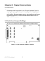
1
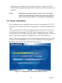
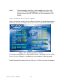
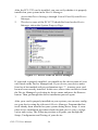
PCI-1723
16-bit, 8-ch., Non-Isolated
Analog Output Card
User Manual
Copyright
The documentation and the software included with this product are copyrighted 2006 by Advantech Co., Ltd. All rights are reserved. Advantech
Co., Ltd. reserves the right to make improvements in the products
described in this manual at any time without notice. No part of this manual may be reproduced, copied, translated or transmitted in any form or
by any means without the prior written permission of Advantech Co., Ltd.
Information provided in this manual is intended to be accurate and reliable. However, Advantech Co., Ltd. assumes no responsibility for its use,
nor for any infringements of the rights of third parties, which may result
from its use.
Acknowledgements
PC-LabCard is a trademark of Advantech Co., Ltd. IBM and PC are
trademarks of International Business Machines Corporation. MS-DOS,
Windows, Microsoft Visual C++ and Visual BASIC are trademarks of
Microsoft Corporation. Intel and Pentium are trademarks of Intel Corporation. Delphi and C++ Builder are trademarks of Inprise Corporation.
All other product names or trademarks are properties of their respective
owners.
Part No. 2003172300
Edition 2
Printed in Taiwan
November 2011
PCI-1723 User Manual
ii
Product Warranty (2 years)
Advantech warrants to you, the original purchaser, that each of its products will be free from defects in materials and workmanship for two years
from the date of purchase.
This warranty does not apply to any products which have been repaired or
altered by persons other than repair personnel authorized by Advantech,
or which have been subject to misuse, abuse, accident or improper installation. Advantech assumes no liability under the terms of this warranty as
a consequence of such events.
Because of Advantech’s high quality-control standards and rigorous testing, most of our customers never need to use our repair service. If an
Advantech product is defective, it will be repaired or replaced at no
charge during the warranty period. For out-of-warranty repairs, you will
be billed according to the cost of replacement materials, service time and
freight. Please consult your dealer for more details.
If you think you have a defective product, follow these steps:
1.
Collect all the information about the problem encountered. (For
example, CPU speed, Advantech products used, other hardware
and software used, etc.) Note anything abnormal and list any on
screen messages you get when the problem occurs.
2.
Call your dealer and describe the problem. Please have your manual, product, and any helpful information readily available.
3.
If your product is diagnosed as defective, obtain an RMA (return
merchandize authorization) number from your dealer. This allows
us to process your return more quickly.
4.
Carefully pack the defective product, a fully-completed Repair and
Replacement Order Card and a photocopy proof of purchase date
(such as your sales receipt) in a shippable container. A product
returned without proof of the purchase date is not eligible for warranty service.
5.
Write the RMA number visibly on the outside of the package and
ship it prepaid to your dealer.
iii
CE
This product has passed the CE test for environmental specifications
when shielded cables are used for external wiring. We recommend the use
of shielded cables. This kind of cable is available from Advantech. Please
contact your local supplier for ordering information.
Technical Support and Assistance
Step 1. Visit the Advantech web site at www.advantech.com/support
where you can find the latest information about the product.
Step 2. Contact your distributor, sales representative, or Advantech's customer service center for technical support if you need additional
assistance. Please have the following information ready before
you call:
- Product name and serial number
- Description of your peripheral attachments
- Description of your software (operating system, version, application software, etc.)
- A complete description of the problem
- The exact wording of any error messages
Packing List
Before setting up the system, check that the items listed below are
included and in good condition. If any item does not accord with the
table, please contact your dealer immediately.
Before you install your PCI-1723 card, please make sure you have the
following necessary components:
• PCI-1723 DA&C card
• PCI-1723 User’s Manual
• Advantech DLL drivers (Included in the companion CD-ROM)
• Wiring cable PCL-10168 (option)
• Wiring board ADAM-3968 (option)
• Personal computer or workstation with a PCI-bus slot (running Windows 2000/95/ 98/NT/ME/XP)
PCI-1723 User Manual
iv
Contents
Chapter
Chapter
1 Introduction ..................................................... 2
1.1
1.2
1.3
Features ............................................................................ 2
Applications ..................................................................... 3
Installation Guide ............................................................. 4
1.4
1.5
1.6
Software Overview........................................................... 6
Device Driver Programming Roadmap ........................... 7
Accessories....................................................................... 9
Figure 1.1:Installation Flow Chart ................................. 5
2 Installation ..................................................... 12
2.1
2.2
Unpacking ...................................................................... 12
Driver Installation .......................................................... 13
2.3
Hardware Installation ..................................................... 15
2.4
Device Setup and Configuration ................................... 17
Figure 2.1:Advantech Automation Software Setup ..... 13
Figure 2.2:Options for Driver Setup ............................ 14
Figure 2.3:Device Name on Device Manager ............. 16
2.4.1
2.4.2
Chapter
Setting Up the Device .................................................. 17
Figure 2.4:Device Manager Dialog Box ...................... 17
Figure 2.5:“Device(s) Found” Dialog Box .................. 18
Configuring the Device ................................................ 18
Figure 2.6:Device Setting Dialog Box ......................... 18
Figure 2.7:Device Name on the List of Devices Box .. 19
3 Signal Connections ........................................ 22
3.1
3.2
Overview ........................................................................ 22
Switch and Jumper Settings .......................................... 22
3.2.1
3.2.2
3.2.3
3.2.4
3.3
Signal Connections ........................................................ 25
3.3.1
3.3.2
3.3.3
3.4
Figure 3.1:Card Connector, Jumper & Switches ......... 22
JP9 ................................................................................ 23
JP1~JP8 ........................................................................ 23
Setting the Time to Reset Analog Outputs .................. 23
Board ID setting ........................................................... 24
Pin Assignment ............................................................ 25
Figure 3.2:I/O Connector Pin Assignments ................. 25
I/O Connector Signal Descriptions ................................ 26
Table 3.1:I/O Connector Signal Descriptions .............. 26
Analog Output Connection .......................................... 27
Figure 3.3:Analog Output Connections ....................... 27
Figure 3.4:Current Mode Diagram .............................. 28
Field Wiring Considerations .......................................... 29
Appendix A Specifications ................................................. 32
A.1
A.2
Analog Output .................................................................... 32
Digital Input /Output ...................................................... 32
v
Table of Contents
A.3
General .......................................................................... 33
Appendix B Block Diagram ............................................... 36
Appendix C Register Structure & Format ....................... 38
C.1
C.2
Overview ........................................................................ 38
I/O Port Address Map ................................................... 38
Table C.1:PCI-1723 Register Format .......................... 39
C.3 D/A ch output data — BASE+00H~0EH ..................... 43
C.4 D/A ch latch data — BASE+00H~0EH......................... 44
C.5 Board ID — BASE+10H ............................................... 45
C.6 All D/A Ch Synchronized Settings — BASE+12H ....... 46
C.7 All D/A Ch Synchronized Status — BASE+12H .......... 46
C.8 DAC Range & Calibration Mode — BASE+14H ......... 47
C.9 DAC Range & Calibration Status — BASE+14H ......... 48
C.10 SADC Control Command for Calibration Function—
BASE+16H 49
C.11 SADC Control Status for Calibration Function—
BASE+16H 50
C.12 Calibration Parameter Strobe — BASE+18H................ 50
C.13 Digital I/O setting — BASE+1AH ................................ 51
C.14 Digital I/O port mode — BASE+1AH........................... 52
C.15 Write Digital Output Command — BASE+1CH........... 52
C.16 Read Digital Input Data — BASE+1CH ....................... 53
C.17 Write Calibration Command — BASE+1EH ................ 53
C.18 Read calibration status — BASE+1EH.......................... 54
C.19 Synchronized Strobe — BASE+20H ............................. 55
C.20 Reset all D/A channels strobe — BASE+22H ............... 55
C.21 Reset the calibration controller strobe — BASE+24H .. 56
C.22 Change D/A channels output type strobe — BASE+26H ..
56
C.23 Select the calibration Ref_V — BASE+28H ................. 57
C.24 Summary ........................................................................ 57
PCI-1723 User Manual
vi
CHAPTER
1
2
Introduction
This chapter gives background information on the PCI-1723.
Sections include:
• Features
• Applications
• Installation Guide
• Software Overview
• Device Driver Programming Roadmap
• Accessories
Chapter 1 Introduction
Thank you for buying the Advantech PCI-1723. The PCI-1723 is a nonisolated multiple channels analog output card for PCI bus, and each analog output channel is equipped with a 16-bit, double-buffered DAC. It
features an auto-calibration function and Board ID.
The PCI-1723 is an ideal solution for industrial applications where multiple analog output channels are required.
The following sections of this chapter will provide further information
about features of the multifunction cards, a Quick Start for installation,
together with some brief information on software and accessories for the
PCI-1723 card.
1.1 Features
• Auto calibration function
• A 16-bit DAC is equipped for each of the analog output channels
• Flexible output range: ±10 V, 0 ~ 20 mA, 4 ~ 20 mA
• Synchronized output function
• Output values kept after system hot reset
• 2-port (16-channel) user-defined digital input/output
• Board ID
The Advantech PCI-1723 offers the following main features:
Auto-Calibration Function
The PCI-1723 provides an auto-calibration function by using a calibration utility. The built-in calibration circuitry of the PCI-1723 corrects gain
and offset errors in analog output channels, thereby eliminating the need
for external equipment and user adjustments.
PCI-1723 User Manual
2
Flexible Voltage Output Range
The PCI-1723 provides a fixed voltage output range of °”10 V to fulfill
your flexible range needed applications. Users can define the specific
voltage output range and output data format via the enclosed software
utility and driver.
Keeping Output Values After System Reset
Users can independently set the eight outputs to different ranges: °”10 V,
0 ~ 20 mA or 4 ~ 20 mA, and all ranges are software selectable. When the
system is hot reset (power not shut down), the PCI-1723 can either retain
the last analog output values, or return to its default configuration,
depending on the jumper setting. This practical function eliminates danger caused by improper operation during unexpected system reset.
Board ID
The PCI-1723 has a built-in DIP Switch that helps define each card’s ID
when multiple PCI-1723 cards have been installed on the same PC chassis. The board ID setting function is very useful when users build their
system with multiple PCI-1723 cards. With correct Board ID settings,
you can easily identify and access each card during hardware configuration and software programming.
Note:
For detailed specifications of the PCI-1723, please
refer to Appendix A, Specifications.
1.2 Applications
• Process control
• Programmable voltage source
• Programmable current sink
• Servo control
• Multiple loop PID control
3
Chapter 1
1.3 Installation Guide
Before you install your PCI-1723 card, please make sure you have the
following necessary components:
• PCI-1723 DA&C card
• PCI-1723 User’s Manual
• Advantech DLL drivers (Included in the companion CD-ROM)
• Wiring cable PCL-10168 (option)
• Wiring board ADAM-3968 (option)
• Personal computer or workstation with a PCI-bus slot (running Windows 2000/95/ 98/NT/ME/XP)
Some other optional components are also available for enhanced operation such as application software ActiveDAQ, GeniDAQ and other thirdparty software packages
After you get the necessary components and maybe some of the accessories for enhanced operation of your Multifunction card, you can then
begin the installation procedure. Figure 1-1 on the next page provides a
concise flow chart to give users a broad picture of the software and hardware installation procedures:
PCI-1723 User Manual
4
Install Driver from CD -ROM, then power -off PC
Install Hardware and power
-on PC
Use driver utility to configure hardware
Use test utility to test hardware
Read examples & driver manual
Start to wri te your own application
Figure 1.1: Installation Flow Chart
5
Chapter 1
1.4 Software Overview
Advantech offers a rich set of DLL drivers, third-party driver support and
application software to help fully exploit the functions of your PCI-1723
card:
• Device Drivers (on the companion CD-ROM)
• LabVIEW driver
• Advantech ActiveDAQ
• Advantech GeniDAQ
Programming choices for DA&C cards: You may use Advantech application software such as Advantech Device Drivers. On the other hand,
advanced users are allowed another option for register-level programming, although not recommended due to its laborious and time-consuming nature.
Device Drivers
The Advantech Device Drivers software is included on the companion
CD-ROM at no extra charge. It also comes with all the Advantech DA&C
cards. Advantech’s Device Drivers features a complete I/O function
library to help boost your application performance. The Advantech
Device Drivers for Windows 2000/95/98/NT/ME/XP works seamlessly
with development tools such as Visual C++, Visual Basic, Inprise C++
Builder and Inprise Delphi.
Register-Level Programming
Register-level programming is available for experienced programmers
who find it necessary to write code directly at the level of the device register. Since register-level programming requires much effort and time, we
recommend that you use the Advantech Device Drivers instead. However, if register-level programming is indispensable, you should refer to
the relevant information in Appendix C, Register Structure and Format,
or to the example codes included on the companion CD-ROM.
PCI-1723 User Manual
6
1.5 Device Driver Programming Roadmap
This section will provide you a roadmap to demonstrate how to build an
application from scratch using Advantech Device Drivers with your
favorite development tools such as Visual C++, Visual Basic, Delphi and
C++ Builder. The step-by-step instructions on how to build your own
applications using each development tool will be given in the Device
Drivers Manual. Moreover, a rich set of example source code is also
given for your reference.
Programming Tools
Programmers can develop application programs with their favorite development tools:
• Visual C++
• Visual Basic
• Delphi
• C++ Builder
For instructions on how to begin programming works in each development tool, Advantech offers a Tutorial Chapter in the Device Drivers
Manual for your reference. Please refer to the corresponding sections in
this chapter on the Device Drivers Manual to begin your programming
efforts. You can also look at the example source code provided for each
programming tool, since they can get you very well oriented.
The Device Drivers Manual can be found on the companion CD-ROM.
Alternatively, if you have already installed the Device Drivers on your
system, The Device Drivers Manual can be readily accessed through the
Start button:
Start/Programs/Advantech Device Driver V2.0/Device Driver Manual
The example source code can be found under the corresponding installation folder such as the default installation path:
\Program Files\Advantech\ADSAPI\Examples
7
Chapter 1
For information about using other function groups or other development
tools, please refer to the Creating Windows 95/NT/2000 Application with
Device Drivers chapter and the Function Overview chapter on the Device
Drivers Manual.
Programming with Device Drivers Function Library
Advantech Device Drivers offer a rich function library that can be utilized
in various application programs. This function library consists of numerous APIs that support many development tools, such as Visual C++,
Visual Basic, Delphi and C++ Builder.
According to their specific functions or services, the APIs can be categorized into several function groups:
• Analog Output Function Group
• Digital Input/Output Function Group
• Counter Function Group
• Port Function Group (direct I/O)
• Event Function Group
For the usage and parameters of each function, please refer to the Function Overview chapter in the Device Drivers Manual.
Troubleshooting Device Drivers Error
Driver functions will return a status code when they are called to perform
a certain task for the application. When a function returns a code that is
not zero, it means the function has failed to perform its designated function. To troubleshoot the Device Drivers error, you can pass the error
code to DRV_GetErrorMessage function to return the error message.
Alternatively, you can refer to the Device Drivers Error Codes Appendix
in the Device Drivers Manual for a detailed listing of Error Codes, Error
IDs and the Error Messages.
PCI-1723 User Manual
8
1.6 Accessories
Advantech offers a complete set of accessory products to support the PCI1723 card. These accessories include:
Wiring Cable PCL-10168
The PCL-10168 shielded cable is specially designed for PCI-1723 cards
to provide high resistance to noise. To achieve a better signal quality, the
signal wires are twisted in such a way as to form a “twisted-pair cable,”
reducing cross talk and noise from other signal sources. Furthermore, its
analog and digital lines are separately sheathed and shielded to neutralize
EMI/EMC problems.
Wiring Board ADAM-3968
The ADAM-3968 is a 68-pin SCSI wiring terminal module for DIN-rail
mounting. This terminal module can be readily connected to the Advantech PC-Lab cards and allow easy yet reliable access to individual pin
connections for the PCI-1723 card.
9
Chapter 1
PCI-1723 User Manual
10
CHAPTER
2
2
Installation
This chapter gives users a package item
checklist, proper instructions for
unpacking and step-by-step procedures
for both driver and card installation.
Sections include:
• Unpacking
• Driver Installation
• Hardware Installation
• Device Setup and Configuration
Chapter 2 Installation
2.1 Unpacking
After receiving your PCI-1723 package, please inspect its contents first.
The package should contain the following items:
• PCI-1723 card
• Companion CD-ROM (Device Drivers included)
• User Manual
The PCI-1723 card harbors certain electronic components vulnerable to
electrostatic discharge (ESD). ESD can easily damage the integrated circuits and certain components if preventive measures are ignored.
Before removing the card from the antistatic plastic bag, you should take
the following precautions to ward off possible ESD damage:
• Touch the metal part of your computer chassis with your hand to discharge the static electricity accumulated on your body. Alternatively,
one can also use a grounding strap.
• Touch the anti-static bag to a metal part of your computer chassis
before opening the bag.
• Take hold of the card only by the metal bracket when removing it out of
the bag.
After taking out the card, you should first:
• Inspect the card for any possible signs of external damage (loose or
damaged components, etc.). If the card is visibly damaged, please
notify our service department or our local sales representative immediately. Do not install a damaged card into your system.
Also, pay extra caution to the following aspects to ensure proper installation:
• Avoid physical contact with materials that could hold static electricity
such as plastic, vinyl and Styrofoam.
PCI-1723 User Manual
12
• Whenever you handle the card, grasp it only by its edges. DO NOT
TOUCH the exposed metal pins of the connector or the electronic components.
Note:
Keep the anti-static bag for future use. You might
need the original bag to store the card if you have to
remove the card from PC or transport it elsewhere.
2.2 Driver Installation
We recommend you to install the driver before you install the PCI-1723
card into your system, since this will guarantee a smooth installation process.
The Advantech Device Drivers Setup program for the PCI-1723 card is
included in the companion CD-ROM that is shipped with your DA&C
card package. Please follow the steps below to install the driver software:
Step 1: Insert the companion CD-ROM into your CD-ROM drive.
Step 2: The Setup program will be launched automatically if you have the
autoplay function enabled on your system. When the Setup Program is
launched, you will see the following Setup Screen.
Figure 2.1: Advantech Automation Software Setup
13
Chapter 2
Note:
If the autoplay function is not enabled on your computer, use Windows Explorer or Windows Run command to execute SETUP.EXE on the companion CDROM.
Step 3: Select the Device Drivers option.
Step 4: Select the specific device then just follow the installation instructions step by step to complete your device driver installation and setup.
Figure 2.2: Options for Driver Setup
For further information on driver-related issues, an online version of the
Device Drivers Manual is available by accessing the following path:
Start/Programs/Advantech Device Drivers V2.0/Device Drivers Manual
PCI-1723 User Manual
14
2.3 Hardware Installation
Make sure you have installed the driver first before you install the card
(please refer to 2.2 Driver Installation).
After the Device Drivers installation is completed, you can then install
the PCI-1723 card into any PCI slot on your computer. However, it is suggested that you refer to the computer user’s manual or related documentation if you have any doubt. Please follow the steps below to install the
card onto your system.
1.
Turn off your computer and unplug the power cord and cables.
TURN OFF your computer before installing or removing any components on the computer.
2.
Remove the cover of your computer.
3.
Remove the slot cover on the back panel of your computer.
4.
Touch the metal part on the surface of your computer to neutralize
the static electricity that might be on your body.
5.
Insert the PCI-1723 card into a PCI slot. Hold the card only by its
edges and carefully align it with the slot. Insert the card firmly into
place. Use of excessive force must be avoided; otherwise, the card
might be damaged.
6.
Fasten the bracket of the PCI card on the back panel rail of the
computer with screws.
7.
Connect appropriate accessories (68-pin cable, wiring terminals,
etc. if necessary) to the PCI card.
8.
Replace the cover of your computer chassis. Re-connect the cables
you removed in step 2.
9.
Plug in the power cord and turn on the computer.
Note:
In case you installed the card without installing the
Device Drivers first, Windows 95/98/ME will recognize your card as an “unknown device” after
rebooting, and will prompt you to provide the necessary driver. You should ignore the prompting
messages (just click the Cancel button) and set up
the driver according to the steps described in 2.2
Driver Installation.
15
Chapter 2
After the PCI-1723 card is installed, you can verify whether it is properly
installed on your system in the Device Manager:
1.
Access the Device Manager through Control Panel/System/Device
Manager.
2.
The device name of the PCI-1723 should be listed on the Device
Manager tab on the System Property Page.
Figure 2.3: Device Name on Device Manager
If your card is properly installed, you should see the device name of your
card listed on the Device Manager tab. If you do see your device name
listed on it but marked with an exclamation sign “!”, it means your card
has not been correctly installed. In this case, remove the card device from
the Device Manager by selecting its device name and press the Remove
button. Then go through the driver installation process again.
After your card is properly installed on your system, you can now configure your device using the Advantech Device Manager Program that has
itself already been installed on your system during driver setup. A complete device installation procedure should include device setup, configuration and testing. The following sections will guide you through the
Setup, Configuration and Testing of your device.
PCI-1723 User Manual
16
2.4 Device Setup and Configuration
The Advantech Device Manager program is a utility that allows you to set
up, configure and test your device, and later stores your settings on the
system registry. These settings will be used when you call the APIs of
Advantech Device Drivers.
2.4.1 Setting Up the Device
1.
To install the I/O device for your card, you must first run the Device
Installation program (by accessing Start/Programs/ Advantech
Device Driver V2.0).
2.
You can then view the device(s) already installed on your system (if
any) on the Installed Devices list box. Since you have not installed
any device yet, you might see a blank list such as the one below
(Fig. 2-4).
Figure 2.4: Device Manager Dialog Box
17
Chapter 2
3.
Scroll down the List of Devices box to find the device that you
wish to install, then click the Add… button to evoke the Device(s)
found dialog box such as one shown in Fig. 2-5. The Device(s)
found dialog box lists all the installed devices on your system.
Select the device you want to configure from the list box and press
the OK button. After you have clicked OK, you will see a Device
Setting dialog box such as the one in Fig. 2-6.
Figure 2.5: “Device(s) Found” Dialog Box
2.4.2 Configuring the Device
4.
On the Device Setting dialog box (Fig. 2-6), you can configure the
voltage output range for the 8 D/A channels.
Figure 2.6: Device Setting Dialog Box
PCI-1723 User Manual
18
When selected as External, the external reference voltage determines the
output voltage range in the following way: By inputting an external reference voltage: -xV, where |x| <= 10, you will get a output voltage range: 0
to xV.
5.
After you have finished configuring the device, click OK and the
device name will appear in the Installed Devices box as seen
below:
Figure 2.7: Device Name on the List of Devices Box
Note:
As we have noted, the device name
“000:PCI-1723 BoardID=0 I/O=6500H”
begins with a device number “000”, which is
specifically assigned to each card. The
device number is passed to the driver to
specify which device you wish to control.
19
Chapter 2
After your card is properly installed and configured, you can click the
Test… button to test your hardware by using the testing utility supplied.
For more detailed information, please refer to Chapter 2 of the Device
Drivers Manual.
You can also find examples on the CD-ROM to speed up your programming.
PCI-1723 User Manual
20
CHAPTER
3
2
Signal Connections
This chapter gives an overview of the
signal connections of PCI-1723.
Sections include:
• Overview
• Switch and Jumper Settings
• Signal Connections
• Field Wiring Considerations
Chapter 3 Signal Connections
3.1 Overview
Maintaining signal connections is one of the most important factors in
ensuring that your application system is sending and receiving data correctly. A good signal connection can avoid unnecessary and costly damage to your PC and other hardware devices. This chapter provides useful
information about how to connect input and output signals to the PCI1723 via the I/O connector.
3.2 Switch and Jumper Settings
The PCI-1723 card has one function switch and five jumper settings.
Figure 3.1: Card Connector, Jumper & Switches
PCI-1723 User Manual
22
3.2.1 JP9
Keep last status after hot reset.
Default configuration.
3.2.2 JP1~JP8
4~20 mA
0~20 mA
3.2.3 Setting the Time to Reset Analog Outputs
Some users will want the capability of clearing each analog output when
the system (or PC) issues a reset signal on the PCI bus. Some users will
want to clear their analog output only as part of system power-on.
The PCI-1723 satisfies both these needs by providing jumper JP1.
Depending on the application, this capability may allow analog outputs to
be "ZERO" without requiring a complete shutdown of processes controlled by the card.
Complete loss of power to the chip clears the chip memory. Thus, no matter how JP1 is set, if the power to the PCI-1723 is disconnected, the analog output initial power-on state will be "ZERO".
23
Chapter 3
3.2.4 Board ID setting
ID3
ID2
ID1
ID0
Board ID
1
1
1
1
0
1
1
1
0
1
1
1
0
1
2
1
1
0
0
3
1
0
1
1
4
1
0
1
0
5
1
0
0
1
6
1
0
0
0
7
0
1
1
1
8
0
1
1
0
9
0
1
0
1
10
0
1
0
0
11
0
0
1
1
12
0
0
1
0
13
0
0
0
1
14
0
0
0
0
15
Note: On: 1, Off: 0
PCI-1723 User Manual
24
3.3 Signal Connections
3.3.1 Pin Assignment
Figure 3-2 shows the pin assignments for the 68-pin I/O connector on the
PCI-1723.
Figure 3.2: I/O Connector Pin Assignments
25
Chapter 3
3.3.2 I/O Connector Signal Descriptions
Table 3.1: I/O Connector Signal Descriptions
Signal
Name
Reference
Direction
Description
Vout<0..3>
AGND
Output
Voltage Output, Channels 0 through 3.
Iout<0..3>
AGND
Output
Current Output, Channels 0 through 3.
AGND
-
-
Analog Ground. The two ground references (AGND and DGND) are connected together on the PCI-1723 card.
DI0<0..15>
DGND
-
Digital Input / Output signals. These
pins are digital input / Output channel
0 to 15.
DGND
-
-
Digital Ground. The two ground references (AGND and DGND) are connected together on the PCI-1723 card.
+12V
DGND
Output
+12 VDC Source (from PCI bus
directly with FUSE protection).
+5V
DGND
Output
+5 VDC Source (from PCI bus directly
with FUSE protection).
PCI-1723 User Manual
26
3.3.3 Analog Output Connection
The PCI-1723 provides eight D/A output channels, Vout_0 ~ Vout_7 and
Iout_0 ~ Iout_7.
Voltage Mode:
Figure 3-3 shows how to make analog output and external reference input
connections on the PCI-1723.
Figure 3.3: Voltage Mode Connections
27
Chapter 3
Current Mode (Sink type):
Caution:
The external voltage should be under 30 V
Ri: Internal resistor = 249 ohm
Vext: External voltage
Isink: The controlled current output (0~20 mA)
Since Isink = Vext / (Ri+RL), RL cannot be higher than | Vext/Imax | - Ri
For Example: Vext = 24 V, Imax = 20 mA
RL max = | 24 V / 20 mA | - 249 = 951 (ohm)
Figure 3.4: Current Mode Connection
PCI-1723 User Manual
28
3.4 Field Wiring Considerations
When you use the PCI-1723 to acquire data from outside, noises in the
environment might significantly affect the accuracy of your measurements if due cautions are not taken. The following measures will be helpful to reduce possible interference running signal wires between signal
sources and the PCI-1723.
The signal cables must be kept away from strong electromagnetic sources
such as power lines, large electric motors, circuit breakers or welding
machines, since they may cause strong electromagnetic interference.
Keep the analog signal cables away from any video monitor, since it can
significantly affect a data acquisition system.
If the cable travels through an area with significant electromagnetic interference, you should adopt individually shielded, twisted-pair wires as the
analog input cable. This type of cable has its signal wires twisted together
and shielded with a metal mesh. The metal mesh should only be connected to one point at the signal source ground.
Avoid running the signal cables through any conduit that might have
power lines in it.
If you have to place your signal cable parallel to a power line that has a
high voltage or high current running through it, try to keep a safe distance
between them. Alternatively, you can place the signal cable at a right
angle to the power line to minimize the undesirable effect.
The signals transmitted on the cable will be directly affected by the quality of the cable. In order to ensure better signal quality, we recommend
that you use the PCL-10168 shielded cable.
29
Chapter 3
PCI-1723 User Manual
30
APPENDIX
A
2
Specifications
This appendix provides information on
the specifications of PCI-1723.
Sections include:
• Analog Output
• Digital Input/Output
• General
Appendix A Specifications
A.1 Analog Output
Channels
8
Resolution
16-bit
Operation mode
Single output, Synchronized output
Output Range
(Internal Reference
only)
-10 ~+10 V, 0 ~ 20 mA, 4 ~ 20 mA
Driving Capability
5 mA
Accuracy
Relative
±6 LSB
Differential
Non-linearity
±6 LSB (monotonic)
Offset
< 6 LSB
Output Impedance
0.1 max.
Throughput
PC dependent, Software update (direct AO)
Settling time
50 us (to °”6 LSB of FSR)
A.2 Digital Input /Output
Input Channels
16 (bi-directional)
Number of ports
2
Input Voltage
Low
0.8 V max.
High
2.0 V min.
Low
0.5 V max. @ +24 mA (sink)
High
2.0 V min. @ -15 mA (source)
Output Voltage
PCI-1723 User Manual
32
A.3 General
I/O Connector Type
68-pin SCSI-II female
Dimensions
175 x 100 mm (6.9" x 3.9")
Power
Consumption
Typical
+5 V @ 850 mA, +12 V @ 600 mA
Max.
+5 V @ 1 A, +12 V @ 700 mA
Temperature
Operation
0 ~ 60°C (32 ~158°F)
(refer to IEC 68-2-1,2)
Storage
-20~85°C (-4~185°F)
Relative Humidity
5~95% RH non-condensing (refer to IEC 68-2-3)
Certifications
CE certified
33
Appendix A
PCI-1723 User Manual
34
APPENDIX
B
2
Block Diagram
This appendix shows the block diagram
for PCI-1723.
Appendix B Block Diagram
Bidirectional
And Latched 8
Bits DIO
DIO[7:0]
Bidirectional
And Latched 8
Bits DIO
DIO[15:8]
Iout 0
16-Bit
DAC 0
Vout 0
Iout 1
16-Bit
DAC 1
PCI Interface
Vout 1
Iout 2
16-Bit
DAC 2
Vout 2
Local Bus
PCI Bus
Iout 3
16-Bit
DAC 3
Vout 3
Iout 4
16-Bit
DAC 4
Vout 4
Iout 5
16-Bit
DAC 5
Vout 5
Iout 6
16-Bit
DAC 6
Vout 6
Iout 7
16-Bit
DAC 7
Vout 7
Auto Calibration Circuit
PCI-1723 User Manual
36
APPENDIX
C
2
Register Structure &
Format
This chapter provides information on
the system settings of UNO-2052.
Sections include:
• Board Connectors and Jumpers
• RS-232 Standard Serial Port
• CAN Serial Port
• Ethernet RJ-45 Connector
• Phoenix Power Connector (PWR)
• PS/2 Keyboard and Mouse Connector
• USB Connector
• VGA Display Connector
• CompactFlash Master/Slave Jumper
Setting
Appendix C Register Structure & Format
C.1 Overview
The PCI-1723 is delivered with an easy-to-use 32-bit Device Drivers for
user programming under the Windows 2000/95/98/NT/ME/XP operating
system. We advise users to program the PCI-1723 using the 32-bit Device
Drivers provided by Advantech to avoid the complexity of low-level registry programming.
The most important consideration in programming the PCI-1723 the register level is to understand the function of the card's registers. The information in the following sections is provided only for users who would
like to do their own low-level programming.
C.2 I/O Port Address Map
The PCI-1723 requires 32 consecutive addresses in the PC's I/O space.
The address of each register is specified as an offset from the card's base
address. For example, BASE+0 is the card's base address and BASE+7 is
the base address plus seven bytes.
Table C-1 shows the function of each register of the PCI-1723 or driver
and its address relative to the card's base address.
PCI-1723 User Manual
38
Table C.1: PCI-1723 Register Format
Base
Adr.
+HEX
00
H
PCI-1723 Register Format
15
14
13
12
11
10
9
8
7
6
5
4
3
2
1
0
DA
11
DA
10
DA
9
DA
8
DA
7
DA
6
DA
5
DA
4
DA
3
DA
2
DA
1
DA
0
DA
11
DA
10
DA
9
DA
8
DA
7
DA
6
DA
5
DA
4
DA
3
DA
2
DA
1
DA
0
DA
11
DA
10
DA
9
DA
8
DA
7
DA
6
DA
5
DA
4
DA
3
DA
2
DA
1
DA
0
DA
11
DA
10
DA
9
DA
8
DA
7
DA
6
DA
5
DA
4
DA
3
DA
2
DA
1
DA
0
DA
11
DA
10
DA
9
DA
8
DA
7
DA
6
DA
5
DA
4
DA
3
DA
2
DA
1
DA
0
DA
11
DA
10
DA
9
DA
8
DA
7
DA
6
DA
5
DA
4
DA
3
DA
2
DA
1
DA
0
DA
11
DA
10
DA
9
DA
8
DA
7
DA
6
DA
5
DA
4
DA
3
DA
2
DA
1
DA
0
DA
11
DA
10
DA
9
DA
8
DA
7
DA
6
DA
5
DA
4
DA
3
DA
2
DA
1
DA
0
DA
11
DA
10
DA
9
DA
8
DA
7
DA
6
DA
5
DA
4
DA
3
DA
2
DA
1
DA
0
DA
11
DA
10
DA
9
DA
8
DA
7
DA
6
DA
5
DA
4
DA
3
DA
2
DA
1
DA
0
DA
11
DA
10
DA
9
DA
8
DA
7
DA
6
DA
5
DA
4
DA
3
DA
2
DA
1
DA
0
DA
11
DA
10
DA
9
DA
8
DA
7
DA
6
DA
5
DA
4
DA
3
DA
2
DA
1
DA
0
W D/A channel 0 output data
DA
15
DA
14
DA
13
DA
12
R D/A channel 0 latch data
DA
15
02
H
DA
14
DA
13
DA
12
W D/A channel 1 output data
DA
15
DA
14
DA
13
DA
12
R D/A channel 1 latch data
DA
15
04
H
DA
14
DA
13
DA
12
W D/A channel 2 output data
DA
15
DA
14
DA
13
DA
12
R D/A channel 2 latch data
DA
15
06
H
DA
14
DA
13
DA
12
W D/A channel 3 output data
DA
15
DA
14
DA
13
DA
12
R D/A channel 3 latch data
DA
15
08
H
DA
14
DA
13
DA
12
W D/A channel 4 output data
DA
15
DA
14
DA
13
DA
12
R D/A channel 4 latch data
DA
15
0A
H
DA
14
DA
13
DA
12
W D/A channel 5 output data
DA
15
DA
14
DA
13
DA
12
R D/A channel 5 latch data
DA
15
DA
14
DA
13
DA
12
39
Appendix C
Table C.1: PCI-1723 Register Format
0C
H
W D/A channel 6 output data
DA
15
DA
14
DA
13
DA
12
DA
11
DA
10
DA
9
DA
8
DA
7
DA
6
DA
5
DA
4
DA
3
DA
2
DA
1
DA
0
DA
11
DA
10
DA
9
DA
8
DA
7
DA
6
DA
5
DA
4
DA
3
DA
2
DA
1
DA
0
DA
11
DA
10
DA
9
DA
8
DA
7
DA
6
DA
5
DA
4
DA
3
DA
2
DA
1
DA
0
R D/A channel 6 latch data
DA
15
0E
H
DA
14
DA
13
DA
12
W D/A channel 7 output data
DA
15
DA
14
DA
13
DA
12
R D/A channel 7 latch data
DA
15
10
H
DA
14
DA
13
DA
12
DA
11
DA
10
DA
9
DA
8
DA
7
DA
6
DA
5
DA
4
DA
3
DA
2
DA
1
DA
0
0
0
0
0
0
0
0
0
0
0
B
D3
BD
2
BD
1
B
D0
X
X
X
X
X
X
X
X
X
SY
N
C
0
0
0
0
0
0
0
0
0
SY
N
C
X
SE
LF
X
X
R1
R0
O
_
G
C
H2
CH
1
C
H0
X
SE
LF
ID
X1
ID
X0
R1
R0
O
_
G
C
H2
CH
1
C
H0
X
X
X
X
X
X
CS
DA
T
CL
K
X
X
X
X
X
X
CS
DA
T
CL
K
W N/A
R Board ID
0
12
H
0
W All D/A channels synchronized setting
X
X
X
X
X
X
R All D/A channels synchronized status
0
14
H
0
0
0
0
0
W DAC range and calibration mode
X
X
X
X
X
X
R DAC range and calibration status
BU
SY
16
H
INI
T
X
X
X
X
W SADC control command for calibration function
X
X
X
X
X
X
X
R SADC control status for calibration function
X
X
X
PCI-1723 User Manual
X
X
X
X
40
18
H
W Calibration parameter strobe
X
X
X
X
X
X
X
X
X
X
X
X
X
X
X
X
X
X
X
X
X
X
X
X
X
X
HD
IO
LD
IO
0
0
0
0
0
0
0
0
0
0
HD
IO
LD
IO
D1
1
D1
0
D9
D8
D7
D6
D5
D4
D3
D2
D1
D0
D1
1
D1
0
D9
D8
D7
D6
D5
D4
D3
D2
D1
D0
X
X
X
X
D7
D6
D5
D4
D3
D2
D1
D0
0
0
0
0
D7
D6
D5
D4
D3
D2
D1
D0
R N/A
1A
H
W Digital I/O port setting
X
X
X
X
R Digital I/O port mode
0
1C
H
0
0
0
W Write digital output command
D1
5
D1
4
D1
3
D1
2
R Read digital input data
D1
5
1E
H
D1
4
D1
3
D1
2
W Write calibration command
X
X
X
X
R Read calibration status
0
0
0
0
41
Appendix C
Table C-1 PCI-1723 register format (Part 3)
Base
Address
+ HEX
20 W
H
22
H
24
H
26
H
28
H
PCI-1723 Register Format
15
14
13 12 11 10
9
8 7
6
4
3
2
1
0
X
X
X
X
X
X
X X X X X X
X
X
X
X
X
X
X
X
X
X
X
X
X X X X X X
X
X
X
X
X X X X X X
X
X
RE R
F_ E
A1 F
_
A
0
R
N/A
W
Reset all D/A channels strobe
X
X
X
X
X
X
X X X X X X
R
N/A
W
Reset the calibration controller strobe
X
X
X
X
X
X
X X X X X X
R
N/A
W
Change D/A channels output type strobe
X
X
X
X
X
X
R
N/A
W
Select the calibration Ref_V
X
R
5
Synchronized strobe
X
X
X
X
X
N/A
PCI-1723 User Manual
42
C.3 D/A ch output data — BASE+00H~0EH
Table C-2 Register for D/A Channels Output Data
Base
Addr.
00 W
H
15 14 13 12 11 10 9 8 7
6
5
4
3
2
1
0
D/A channel 0 output data
02
H
W
DA D DA D DA DA D D DA DA DA DA DA DA DA DA0
15 A1 13 A1 11 10 A A8 7
6 5
4
3
2
1
4
2
9
D/A channel 1 output data
04
H
W
DA D DA D DA DA D D DA DA DA DA DA DA DA DA0
15 A1 13 A1 11 10 A A8 7
6 5
4
3
2
1
4
2
9
D/A channel 2 output data
06
H
W
DA D DA D DA DA D D DA DA DA DA DA DA DA DA0
3
2
1
15 A1 13 A1 11 10 A A8 7
6 5
4
4
2
9
D/A channel 3 output data
08
H
W
DA D DA D DA DA D D DA DA DA DA DA DA DA DA0
15 A1 13 A1 11 10 A A8 7
6 5
4
3
2
1
4
2
9
D/A channel 4 output data
0A W
H
0C W
H
0E W
H
DA D DA D DA DA D D DA DA DA DA DA DA DA DA0
15 A1 13 A1 11 10 A A8 7
6 5
4
3
2
1
4
2
9
D/A Channel 5 output data
DA D DA D DA DA D D DA DA DA DA DA DA DA DA0
6 5
4
3
2
1
15 A1 13 A1 11 10 A A8 7
4
2
9
D/A channel 6 output data
DA D DA D DA DA D D DA DA DA DA DA DA DA DA0
15 A1 13 A1 11 10 A A8 7
6 5
4
3
2
1
4
2
9
D/A channel 7 output data
DA D DA D DA DA D D DA DA DA DA DA DA DA DA0
15 A1 13 A1 11 10 A A8 7
6 5
4
3
2
1
4
2
9
DA15 ~ DA0 D/A channel output data
DA0 the least significant bit (LSB) of the D/A data
DA15 the most significant bit (MSB)
43
Appendix C
C.4 D/A ch latch data — BASE+00H~0EH
Table C-3 Register for D/A Channels Latch Data
Base
Addr.
00 R
H
15 14 13 12 11
10 9
8
7
6
5
4
3
2
1 0
D/A channel 0 latch data
02
H
R
DA DA DA DA DA DA DA DA DA DA DA DA DA DA D D
15 14 13 12 11 10 9
8 7 6 5 4 3 2 A A
1 0
D/A channel 1 latch data
04
H
R
DA DA DA DA DA DA DA DA DA DA DA DA DA DA D D
15 14 13 12 11 10 9
8 7 6 5 4 3 2 A A
1 0
D/A channel 2 latch data
06
H
R
DA DA DA DA DA DA DA DA DA DA DA DA DA DA D D
15 14 13 12 11 10 9
8 7 6 5 4 3 2 A A
1 0
D/A channel 3 latch data
08
H
R
DA DA DA DA DA DA DA DA DA DA DA DA DA DA D D
15 14 13 12 11 10 9
8 7 6 5 4 3 2 A A
1 0
D/A channel 4 latch data
0A R
H
0C R
H
0E R
H
DA DA DA DA DA DA DA DA DA DA DA DA DA DA D D
15 14 13 12 11 10 9
8 7 6 5 4 3 2 A A
1 0
D/A channel 5 latch data
DA DA DA DA DA DA DA DA DA DA DA DA DA DA D D
15 14 13 12 11 10 9
8 7 6 5 4 3 2 A A
1 0
D/A channel 6 latch data
DA DA DA DA DA DA DA DA DA DA DA DA DA DA D D
15 14 13 12 11 10 9
8 7 6 5 4 3 2 A A
1 0
D/A channel 7 latch data
DA DA DA DA DA DA DA DA DA DA DA DA DA DA D D
15 14 13 12 11 10 9
8 7 6 5 4 3 2 A A
1 0
DA15 ~ DA0 D/A channel latch data
DA0 the least significant bit (LSB) of the D/A data
DA15 the most significant bit (MSB)
PCI-1723 User Manual
44
C.5 Board ID — BASE+10H
The PCI-1723 offers Board ID register BASE+10H. With correct Board
ID settings, users can easily identify and access each card during hardware configuration and software programming.
Table C-4 Register for Board ID
Base
Addr.
10 R
H
15 14 13 12 11
10 9
8
7
6
5
4
3
2
1
0
0
0
0
0
0
0
BD BD BD BD
3 2 1 0
Board ID
0
0
0
0
0
0
BD3 ~ DB0 Board ID
BD0
LSB of the Board ID
BD3
MSB of the Board ID
BD3
1
1
1
1
1
1
1
1
0
0
0
0
0
0
0
0
BD2
1
1
1
1
0
0
0
0
1
1
1
1
0
0
0
0
BD1
1
1
0
0
1
1
0
0
1
1
0
0
1
1
0
0
45
BD0
1
0
1
0
1
0
1
0
1
0
1
0
1
0
1
0
Board ID
15
14
13
12
11
10
9
8
7
6
5
4
3
2
1
0
Appendix C
C.6 All D/A Ch Synchronized Settings — BASE+12H
The PCI-1723 provides an innovate function in which all D/A channels
can output their data in synchronization.
Table C-5 Register for all D/A channels synchronized setting
Base
Addr.
12 W
H
15
14
13
12
11
10
9
8
7
6
5
4
3
2
1
0
X
X
X
X
X
X
SY
NC
All D/A channels synchronized setting
X
X
X
X
X
X
X
X
X
SYNC
D/A channels output synchronous
0
Disable (all D/A channels output directly)
1
Enable
Note:
Be sure to enable the synchronize function by writing the value to this
register first. Next, write the specific data into BASE+00H ~ 0FH. Lastly,
write any value to BASE+12H to synchronize all D/A channels.
On the other hand, it you did not enable the synchronize function by writing the value to this register first, all the specific data which was written
to BASE+00H ~ 0FH will be output immediately!
C.7 All D/A Ch Synchronized Status — BASE+12H
Table C-6 Register for All D/A Channels Synchronized Status
Base
Addr.
12 R
H
15 14 13 12 11
10 9
8
7
6
5
4
3
2
1
0
0
0
0
0
0
0
SY
NC
All D/A channels synchronized status
0
0
0
0
0
0
0
0
0
SYNC
D/A channels output synchronous
0
Disable (all D/A channels output directly)
1
Enable
PCI-1723 User Manual
46
C.8 DAC Range & Calibration Mode — BASE+14H
Table C-7 Register for DAC Range and Calibration Mode
Base
Addr.
14 W
H
15 14 13 12 11 10 9
8
7
6
5
4
3
2
1
0
SE X
LF
X
R1 R0 O_ CH CH CH
G 2 1 0
DAC range and calibration mode
X
X
X
X
X
X
X
CH2 ~ CH0 Select D/A channel
000
Channel 0
001
Channel 1
010
Channel 2
011
Channel 3
100
Channel 4
101
Channel 5
110
Channel 6
111
Channel 7
O_G
Calibrate gain or offset
0
Gain
1
Offset
R1 ~ R0 Select D/A range
00
± 10V
01
N/A
10
0 ~ 20 mA
11
4 ~ 20 mA
SELF
Select normal or self-system calibration
0
Normal calibration
1
Self-system offset calibration
47
Appendix C
Note:
Once you want to change the range of
the specific channel, be sure to write the
value to this register first. After that,
write any value to BASE+26H to strobe
the change.
C.9 DAC Range & Calibration Status — BASE+14H
Table C-8 Register for DAC range and calibration status
Base
Addr.
14 R
H
15 14 13 12 11 10 9
8
7
6
5
4
3
2
1
0
DAC range and calibration status
BU INI X
SY T
X
X
X
X
SE ID ID R1 R0 O_ CH CH CH
LF X1 X0
G 2 1 0
CH2 ~ CH0 Select D/A channel
000
Channel 0
001
Channel 1
010
Channel 2
011
Channel 3
100
Channel 4
101
Channel 5
110
Channel 6
111
Channel 7
O_G
Calibrate gain or offset
0
Gain
1
Offset
R1 ~ R0 Select D/A range
00
± 10V
01
N/A
PCI-1723 User Manual
48
10
0 ~ 20 mA
11
4 ~ 20 mA
SELF
Select normal or self-system calibration
0
Normal calibration
1
Self-system offset calibration
INIT
Initial the calibration controller
0
Idle
1
Processing
BUSY
Calibration controller busy flag
0
Idle
1
Busy
IDX1 ~ IDX0 Calibration procedure index
00
Read/Write calibration status
01
Write calibration parameter
10
Change D/A channels output type and reload the parameters
11
N/A
C.10 SADC Control Command for Calibration Function— BASE+16H
The PCI-1723 uses SADC (serial analog to digital converter) for the calibration function. Please refer to the Burr-Brown ADS7822 data sheet for
the chipset detailed information (CD-ROM:\Documents\Component
Specification\ ADS7822.PDF).
Table C-9 Register for SADC control command for calibration function
Base
Addr.
16 W
H
CS
15 14 13 12 11 10 9
8
7
6
5
4
3
2
1
0
X
X
CS DA CL
T K
SADC control command for calibration function
X
X
X
X
X
X
X
X
X
X
X
SADC chip select (active low)
49
Appendix C
DAT
SADC serial data
CLK
SADC clock
C.11 SADC Control Status for Calibration Function—
BASE+16H
Table C-10 Register for SADC control for calibration function
Base
Addr.
16 R
H
15 14
13
12 11
10
9
8
7
6
5
4
3
2
1
0
X
X
X
CS DA CL
T K
SADC control status for calibration function
X
X
X
X
X
X
X
X
X
X
CS
SADC chip select (active low)
DAT
SADC serial data
CLK
SADC clock
C.12 Calibration Parameter Strobe — BASE+18H
Write any values to BASE+18H after finishing the calibration procedure
to save all the D/A channels’ parameters into the EEPROM.
Table C-11 Register for calibration parameter strobe
Base
Addr.
18 W
H
15 14 13 12 11 10 9
8
7
6
5
4
3
2
1
0
X
X
X
X
X
X
X
X
X
Calibration parameter strobe
X
X
X
PCI-1723 User Manual
X
X
X
X
50
Note:
If you want to calibrate the range of the specific channel,
be sure to write the value to BASE+14H first. Next, write
the data to BASE+1EH for calibration purposes. Lastly,
write the value to this register to strobe the parameters into
EEPROM.
C.13 Digital I/O setting — BASE+1AH
Table C-12 Register for digital I/O port setting
Base
Addr.
1A W
H
15 14 13 12 11
10 9
8
7
6
5
4
3
2
1
0
X
X
X
X
X
X
X
X
HD LDI
IO O
Digital I/O port setting
X
X
X
X
X
X
LDIO
Setting the Low byte DIO port
0
Output
1
Input
HDIO
Setting the High byte DIO port
0
Output
1
Input
Note:
The port that is setup as output supports ‘read back’ function.
The port that setup as input supports ‘mask’ function.
Above registries must be accessed by one word at a time.
51
Appendix C
C.14 Digital I/O port mode — BASE+1AH
Table C-13 Register for digital I/O port modes
Base
Addr.
1A R
H
15 14 13 12 11 10 9
8
7
6
5
4
3
2
1
0
0
0
0
0
0
0
0
HD LDI
IO O
Digital I/O port mode
0
0
0
0
0
0
0
LDIO
Status of the Low byte DIO port
0
Output
1
Input
HDIO
Status of the High byte DIO port
0
Output
1
Input
C.15 Write Digital Output Command — BASE+1CH
Table C-14 Register for write digital output command
Base
Addr.
1C W
H
15 14 13 12 11 10 9
8
7
6
5
4
3
2
1
0
Write digital output command
D1 D1 D1 D1 D1 D1 D9 D8 D7 D6 D5 D4 D3 D2 D1 D0
5 4 3 2 1 0
D15 ~ D0 Digital output data
D0
LSB of the output data
D15
MSB of the output data
PCI-1723 User Manual
52
C.16 Read Digital Input Data — BASE+1CH
Table C-15 Register for Read Digital Input Data
Base
Addr.
1C R
H
15 14 13 12 11 10 9
8
7
6
5
4
3
2
1
0
Read digital input data
D1 D1 D1 D1 D1 D1 D9 D8 D7 D6 D5 D4 D3 D2 D1 D0
5 4 3 2 1 0
D15 ~ D0 Digital input data
D0
LSB of the input data
D15
MSB of the input data
C.17 Write Calibration Command — BASE+1EH
Table C-16 Register for write calibration command
Base
Addr.
1E W
H
15 14
13 12 11
10 9
8
7
6
5
4
3
2
1
0
X
D7 D6 D5 D4 D3 D2 D1 D0
Write calibration command
X
X
X
X
X
X
X
D7 ~ D0 Calibration result data
D0
the least significant bit (LSB) of the data
D7
the most significant bit (MSB)
Note:
If you want to calibrate the range of the specific
channel, be sure to write the value to BASE+14H
first. Next, write the data to this register for calibration purposes. Lastly, write the value to BASE+18H
to strobe the parameters into EEPROM.
53
Appendix C
C.18 Read calibration status — BASE+1EH
Table C-17 Register for read calibration status
Base
Addr.
1E R
H
15 14 13 12 11 10 9
8
7
6
5
4
3
2
1
0
0
D7 D6 D5 D4 D3 D2 D1 D0
Read calibration status
0
0
0
0
0
0
0
D7 ~ D0 Calibration result data
D0
the least significant bit (LSB) of the data
D7
the most significant bit (MSB)
PCI-1723 User Manual
54
C.19 Synchronized Strobe — BASE+20H
Write any values to BASE+20H to synchronize all D/A channels.
Table C-18 Register for synchronized strobe
Base
Addr.
20 W
H
15 14 13 12 11 10 9
8
7
6
5
4
3
2
1
0
X
X
X
X
X
X
X
X
X
Synchronized strobe
X
X
Note:
X
X
X
X
X
Be sure to enable the synchronize function by writing
the value to BASE+12H first. Next, write the specific
data into BASE+00H ~ 0FH. Lastly, write any value to
this register to synchronize all D/A channels.
On the other hand, it you did not enable the synchronize function by writing the value to BASE+12H first,
all the specific data which was written to BASE+00H ~
0FH will be output immediately!
C.20 Reset all D/A channels strobe — BASE+22H
Write any values to BASE+22H to reset all D/A channels.
Table C-19 Register for reset all D/A channels strobe
Base
Addr.
22 W
H
15 14 13 12 11 10 9
8
7
6
5
4
3
2
1
0
X
X
X
X
X
X
X
X
X
Reset all D/A channels strobe
X
X
X
X
X
X
X
55
Appendix C
C.21 Reset the calibration controller strobe —
BASE+24H
Write any values to BASE+24H to reset the calibration controller.
Table C-20 Register for reset the calibration controller strobe
Base
Addr.
24 W
H
15 14 13 12 11 10 9
8
7
6
5
4
3
2
1
0
X
X
X
X
X
X
X
Reset the calibration controller strobe
X
X
X
X
X
X
X
X
X
C.22 Change D/A channels output type strobe —
BASE+26H
Write any values to BASE+26H to change D/A channel output type.
Table C-21 Register for change D/A channels output type strobe
Base
Addr.
26 W
H
15 14 13 12 11 10 9
8
7
6
5
4
3
2
1
0
X
X
X
X
X
X
Change D/A channels output type strobe
X
X
X
Note:
PCI-1723 User Manual
X
X
X X
X
X
X
Once you want to change the range of the
specific channel, be sure to write the value
to BASE+14H first. After that, write any
value to this register to strobe the change.
56
C.23 Select the calibration Ref_V — BASE+28H
Table C-22 Register for select the calibration Ref_V
Base
Addr.
28 W
H
15
14
13
12
11
10
9
8
7
6
5
4
3
2
1
0
X
X
X
X
X
X
X
X
RE RE
F_ F_
A1 A0
Select the calibration Ref_V
X
X
X
X
X
X
REF_A1 ~ REF_A0 Ref_V (reference voltage) index
00
-10 V
01
0V
10
N/A
11
+10 V
C.24 Summary
Calibrate the range of the specific channel
Step 1: BASE+14H
Step 2: BASE+1EH
Step 3: BASE+18H
Change the range of the specific channel
Step 1: BASE+14H
Step 2: BASE+26H
Synchronized output channel
Step 1: BASE+12H
Step 2: BASE+00H ~ 0FH
Step 3: BASE+20H
57
Appendix C
PCI-1723 User Manual
58