1
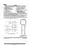
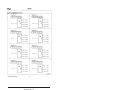
NOTICE The drivers and utilities for Octagon products, previously provided on a CD, are now in a self-extracting zip file located at the Octagon Systems web site on the product-specific page. Download this file to a separate directory on your hard drive, then double click on it to extract the files. All references in this manual to files and directories on the CD now refer to files in the Utilities zip file. 5720 User’s Manual Doc. #03363 Rev 0494 OCTAGON SYSTEMS CORPORATION® 6510 W. 91st Ave. Westminster, CO 80030 Tech. Support: 303–426–4521 COPYRIGHT Copyright 1992–94—Octagon Systems Corporation. All rights reserved. However, any part of this document may be reproduced, provided that Octagon Systems Corporation is cited as the source. The contents of this manual and the specifications herein may change without notice. TRADEMARKS Micro PC, PC SmartLink, Octagon Systems Corporation®, the Octagon logo and the Micro PC logo are trademarks of Octagon Systems Corporation. QuickBASIC® is a registered trademark of Microsoft Corporation. NOTICE TO USER The information contained in this manual is believed to be correct. However, Octagon assumes no responsibility for any of the circuits described herein, conveys no license under any patent or other right, and makes no representations that the circuits are free from patent infringement. Octagon makes no representation or warranty that such applications will be suitable for the use specified without further testing or modification. Octagon Systems Corporation general policy does not recommend the use of its products in life support applications where the failure or malfunction of a component may directly threaten life or injury. It is a Condition of Sale that the user of Octagon products in life support applications assumes all the risk of such use and indemnifies Octagon against all damage. IMPORTANT! Please read before installing your product. Octagon's products are designed to be high in performance while consuming very little power. In order to maintain this advantage, CMOS circuitry is used. CMOS chips have specific needs and some special requirements that the user must be aware of. Read the following to help avoid damage to your card from the use of CMOS chips. Using CMOS Circuitry – 1 Using CMOS Circuitry in Industrial Control Industrial computers originally used LSTTL circuits. Because many PC components are used in laptop computers, IC manufacturers are exclusively using CMOS technology. Both TTL and CMOS have failure mechanisms, but they are different. This section describes some of the common failures which are common to all manufacturers of CMOS equipment. However, much of the information has been put in the context of the Micro PC. Octagon has developed a reliable database of customer-induced, field failures. The average MTBF of Micro PC cards exceeds 11 years, yet there are failures. Most failures have been identified as customer-induced, but there is a small percentage that cannot be identified. As expected, virtually all the failures occur when bringing up the first system. On subsequent systems, the failure rate drops dramatically. ■ Approximately 20% of the returned cards are problem-free. These cards, typically, have the wrong jumper settings or the customer has problems with the software. This causes frustration for the customer and incurs a testing charge from Octagon. ■ Of the remaining 80% of the cards, 90% of these cards fail due to customer misuse and accident. Customers often cannot pinpoint the cause of the misuse. ■ Therefore, 72% of the returned cards are damaged through some type of misuse. Of the remaining 8%, Octagon is unable to determine the cause of the failure and repairs these cards at no charge if they are under warranty. The most common failures on CPU cards are over voltage of the power supply, static discharge, and damage to the serial and parallel ports. On expansion cards, the most common failures are static discharge, over voltage of inputs, over current of outputs, and misuse of the CMOS circuitry with regards to power supply sequencing. In the case of the video cards, the most common failure is to miswire the card to the flat panel display. Miswiring can damage both the card and an expensive display. ■ Multiple component failures - The chance of a random component failure is very rare since the average MTBF of an Octagon card is greater than 11 years. In a 7 year study, Using CMOS Circuitry – 2 Octagon has never found a single case where multiple IC failures were not caused by misuse or accident. It is very probable that multiple component failures indicate that they were user-induced. ■ Testing “dead” cards - For a card that is “completely nonfunctional”, there is a simple test to determine accidental over voltage, reverse voltage or other “forced” current situations. Unplug the card from the bus and remove all cables. Using an ordinary digital ohmmeter on the 2,000 ohm scale, measure the resistance between power and ground. Record this number. Reverse the ohmmeter leads and measure the resistance again. If the ratio of the resistances is 2:1 or greater, fault conditions most likely have occurred. A common cause is miswiring the power supply. ■ Improper power causes catastrophic failure - If a card has had reverse polarity or high voltage applied, replacing a failed component is not an adequate fix. Other components probably have been partially damaged or a failure mechanism has been induced. Therefore, a failure will probably occur in the future. For such cards, Octagon highly recommends that these cards be replaced. ■ Other over-voltage symptoms - In over-voltage situations, the programmable logic devices, EPROMs and CPU chips, usually fail in this order. The failed device may be hot to the touch. It is usually the case that only one IC will be overheated at a time. ■ Power sequencing - The major failure of I/O chips is caused by the external application of input voltage while the Micro PC power is off. If you apply 5V to the input of a TTL chip with the power off, nothing will happen. Applying a 5V input to a CMOS card will cause the current to flow through the input and out the 5V power pin. This current attempts to power up the card. Most inputs are rated at 25 mA maximum. When this is exceeded, the chip may be damaged. ■ Failure on power-up - Even when there is not enough current to destroy an input described above, the chip may be destroyed when the power to the card is applied. This is due to the fact that the input current biases the IC so that it acts as a forward biased diode on power-up. This type of failure is typical on serial interface chips. Using CMOS Circuitry – 3 ■ Serial and parallel - Customers sometimes connect the serial and printer devices to the Micro PC while the power is off. This can cause the failure mentioned in the above section, Failure upon power-up. Even if they are connected with the Micro PC on, there can be another failure mechanism. Some serial and printer devices do not share the same power (AC) grounding. The leakage can cause the serial or parallel signals to be 20-40V above the Micro PC ground, thus, damaging the ports as they are plugged in. This would not be a problem if the ground pin is connected first, but there is no guarantee of this. Damage to the printer port chip will cause the serial ports to fail as they share the same chip. ■ Hot insertion - Plugging cards into the card cage with the power on will usually not cause a problem. (Octagon urges that you do not do this!) However, the card may be damaged if the right sequence of pins contacts as the card is pushed into the socket. This usually damages bus driver chips and they may become hot when the power is applied. This is one of the most common failures of expansion cards. ■ Using desktop PC power supplies - Occasionally, a customer will use a regular desktop PC power supply when bringing up a system. Most of these are rated at 5V at 20A or more. Switching supplies usually require a 20% load to operate properly. This means 4A or more. Since a typical Micro PC system takes less than 2A, the supply does not regulate properly. Customers have reported that the output can drift up to 7V and/or with 7-8V voltage spikes. Unless a scope is connected, you may not see these transients. ■ Terminated backplanes - Some customers try to use Micro PC cards in backplanes that have resistor/capacitor termination networks. CMOS cards cannot be used with termination networks. Generally, the cards will function erratically or the bus drivers may fail due to excessive output currents. ■ Excessive signal lead lengths - Another source of failure that was identified years ago at Octagon was excessive lead lengths on digital inputs. Long leads act as an antenna to pick up noise. They can also act as unterminated transmission lines. When 5V is switch onto a line, it creates a transient waveform. Octagon has seen submicrosecond pulses of 8V or more. The solution is to place a capacitor, for example 0.1 µF, across the switch contact. This will also eliminate radio frequency and other high frequency pickup. Using CMOS Circuitry – 4 TABLE OF CONTENTS PREFACE ........................................................................ 1 Conventions Used In This Manual ................................................... 1 Symbols and Terminology ................................................................. 2 Technical Support .............................................................................. 3 CHAPTER 1: OVERVIEW .............................................. 5 Description ......................................................................................... 5 Major Features ................................................................................... 5 CHAPTER 2: INSTALLATION ....................................... 7 Description ......................................................................................... 7 Equipment .......................................................................................... 7 Jumper Settings ................................................................................. 8 Base Addresses ............................................................................ 8 5720 Quick start ................................................................................. 9 Troubleshooting ................................................................................ 13 CHAPTER 3 : ANALOG INPUTS ................................ 15 Description ....................................................................................... Voltage Range ................................................................................... Calibration ........................................................................................ Channel Selection & A/D Conversion ............................................. Polling and Interrupts .............................................................. 15 16 16 17 18 CHAPTER 4: DIGITAL I/O ........................................... 21 Description ....................................................................................... Programming Example .................................................................... Interfacing to an Opto Module Rack .............................................. Interfacing to Switches or Other Devices ...................................... 21 23 24 25 CHAPTER 5: TECHNICAL DATA ................................ 27 Technical Specifications .................................................................. Jumper Configurations .................................................................... Connector Pinouts ............................................................................ PC Bus Pinouts ................................................................................. iii 27 28 29 31 APPENDIX A: 82C55 DATA SHEET ........................... 33 WARRANTY iv PREFACE This manual is a guide to the proper configuration, installation, and operation of your 5720 Analog Input Card. Installation instructions, card mapping information, jumpering options and technical specifications are described in the main section of the manual. Additional programming examples and technical information are included in the appendices. The 5720 Analog Input Card is part of the Octagon Micro PC system. It is designed to be used with any of the Micro PC Control Cards. You can use your 5720 card in conjunction with other Micro PC expansion cards, tailoring your system for a wide variety of applications. The 5720 card can also be used in an IBM compatible PC. Micro PC cards are too tall to fit in an XT, but will fit in AT industrial sized and other AT–size cases. All Micro PC products are modular, so creating a system is as easy as selecting and plugging in the products you need. CONVENTIONS USED IN THIS MANUAL 1. Information which appears on your screen (output from your system, commands or data that you key in) is shown in a different type face. Octagon 5016 BIOS vers x.xx Copyright (c) 1991, Octagon Systems, Corp. All Rights Reserved. 2. Italicized refers to information that is specific to your particular system or program, e.g., Enter filename means enter the name of your file. 3. Warnings always appear in this format: WARNING: The warning message appears here. Preface – 1 4. Paired angle brackets are used to indicate a specific key on your keyboard, e.g., <ESC> means the escape key; <CTRL> means the control key; <F1> means the F1 function key. 5. All addresses are given in hexadecimal. SYMBOLS AND TERMINOLOGY Throughout this manual, the following symbols and terminology are used: W[ – ] Denotes a jumper block and the pins to connect. BIOS drive The solid–state disk which contains the system BIOS and ROM–DOS. Control Card Contains the CPU, memory, and operating system and controls the operation of all the extension cards. DRAM Dynamic Random Access Memory devices. DRAMs provide volatile memory with unlimited read and write cycles. Expansion Card The expansion cards add I/O functions to the Micro PC system, such as analog input/ output, digital input/output, motion control, display, and so on. Flash EPROM Electrically erasable EPROM which allows approximately 10,000 writes. Memory device The type of static RAM, DRAM, flash EPROM or EPROM specified for either volatile or nonvolatile memory. PC SmartLINK A serial communications software package designed by Octagon for use with the 5720 8– Bit Analog Input Card. Refers to all versions of PC SmartLINK. Preface – 2 ROM Read Only Memory devices. ROMs provide nonvolatile memory, have a limited number of write cycles, and include EPROMs, EEPROMs, and flash EPROMs. ROM–DOS DOS operating system included in Micro PC ROM. Solid–State Disk (SSD) A simulated disk using a high speed solid– state memory device, for example flash EPROM, EEPROM, or static RAM. Static RAM Static Random Access Memory device. Static RAMs provide volatile memory with unlimited read and write cycles. They may be used with a battery back–up module. TTL Compatible Transistor transistor logic compatible; 0–5V logic levels. H The suffix “H” denotes a hexadecimal number. A decimal number has no prefix or suffix. For example, 1000H and 4096 are equivalent. TECHNICAL SUPPORT If you have a question about the 5720 Analog Input Card and cannot find the answer in this manual, call Technical Support. They will be ready to give you the assistance you need. When you call, please have the following at hand: Your 5720 User’s Manual A description of your problem. The direct line to Technical Support is 303–426–4521. Preface – 3 This page intentionally left blank. Preface – 4 CHAPTER 1 OVERVIEW DESCRIPTION The 5720 8–Bit Analog Input Card is designed for low cost applications requiring analog input and digital control. It has an 8– channel analog to digital converter with 8–bit resolution. The 8– single ended channels are multiplexed under software control. The 5720 has a conversion time of 8.5 uS and a throughput of 100,000 samples per second. The input range of the 5720 is 0–5V. Inputs are protected from overload up to +/–16V even when the power is off. A precision 5V reference is provided and never needs calibration. The 5720 also has 24 digital I/O lines. These lines may be programmed as either inputs or outputs in groups of four and eight for direct connection to an opto rack for interface with high current AC and DC voltages. The 5720 A/D Card measures 4.5 in. x 4.9 in. and uses one slot of the Micro PC card cage. MAJOR FEATURES High Performance A/D Converter • 8–bit resolution • 8 single–ended inputs • 0–5V input range • +/–16V over voltage protection • 100,000 samples per second 24 Digital I/O Lines • Configured and controlled by software • 24 lines that may be independently configured as inputs or outputs in groups of four and eight • All I/O lines may directly interface with optical relays Access Indicator • Front mounted, high visibility LED • Flashes briefly when the card is accessed Overview – 5 Easy I/O Address Selection • Jumper selectable I/O addresses • Up to 8 cards may be used in a system Overview – 6 CHAPTER 2 INSTALLATION DESCRIPTION This chapter includes information on setting the base address, selecting the interrupt source and interrupt request line and installing the 5720 8–Bit Analog Input Card in the card cage. This card is designed to be used with Octagon’s Micro PC system. It uses one card slot and plugs directly into the Micro PC backplane (motherboard). EQUIPMENT You will need the following equipment (or equivalent) to use your 5720: • • • • • 5720 8–Bit Analog Input Card Micro PC Control Card Micro PC Card Cage Power Module PC SmartLINK You may also want to use: • • • • • AIN–5B Signal Conditioning Board STB–26 Terminal Board MUX–16 Analog Multiplexer Board ITB–8/16 or ITB–16/8 Level Conversion Board Opto Rack Before installing the 5720 A/D Card, refer to figure 2–1 for the location of various connectors and jumpers Installation – 7 Base Address Select & Interrupt Select LED Access Indicator U7 U5 U1 U8 J2 Analog Input J1 Digital I/O W1 1 2 U9 U2 U6 U4 U3 Y1 Figure 2–1—5720 Component Diagram JUMPER SETTINGS The 5720 is shipped with default jumper connections in place. If you are setting up the 5720 for the first time, we recommend you not change the jumpers until you have completed the installation procedures and the DEMO program. Base Addresses The base address of the 5720 is configurable via jumpers and is set to 100H at the factory. If there is another card in your system with a base address of 100H, you must use a different base address Installation – 8 (or change the address of the other card). To change the base address, change the configuration of jumper block W1. The table below lists the jumper configurations and corresponding base addresses: Base Address Select: W1 Pins Jumpered Base Address [1-2] [3-4] [5-6]* 100H [1-2] [3-4] 110H [1-2] [5-6] 120H [1-2] 130H [3-4] [5-6] 140H [3-4] 150H [5-6] 160H Not jumpered 170H * = default 5720 QUICK START The following instructions are a quick overview of installing and using the 5720 card with factory default settings. For more information on the specific features of the card, please refer to the appropriate chapter. WARNING: The 5720 card contains static sensitive CMOS components. The greatest danger occurs when the card is plugged into a card cage. The 5720 card becomes charged by the user and the static discharges to the backplane from the pin closest to the card connector. If that pin happens to be Installation – 9 an input pin, even TTL inputs may be damaged. To avoid damaging your card and its components: 1. Ground yourself before handling the 5720 card. 2. Disconnect power before removing or inserting the 5720 card. Take care to correctly position the 5720 in the card cage. The Vcc and ground signals must match those on the backplane. Figure 2–2 shows the relative positions of the 5720 and the backplane. A31 B31 Card Edge Pins A31 & B31 5720 8-Bit Analog Input Card Micro-PC Motherboard A1 B1 Card Edge Pins A1 & B1 Figure 2–2 — Edge Connector Orientation 1. Install the 5720 in the Micro PC card cage. 2. Position the cage so that the backplane is away from you, the power module is to the right, and the open side of the cage is closest to you. The lettering on the backplane should be right side up ( for example, you should be able to read “A31” on the backplane), with the words OCTAGON SYSTEMS CORP. running vertically along the left side of the backplane. This position is “feet down” for a table mount cage and “feet back” for a rear mount. Installation – 10 3. Slide the 5720 into the card cage. You may use any slot. The components on the card should face to the left. 4. Turn on the card cage power. 5. Execute the following example program: 10 20 OUT 256,255 PRINT INP(256) Explanation Line 10 Start CH0. Base address is 256. Line 20 Read CH0 This routine represents the simplest way a single analog sample may be taken. The BASIC commands are generic and should be compatable with any BASIC supporting standard syntax. The following is a functional diagram of the 5720 and depicts how the analog input and digital I/O features are inter-related: Installation – 11 +5 A: 0-7 10K A +5 B: 0-7 10K C +5 C: 0-7 10K Bus Connector Buffers & Decode Logic B Analog Input 0-5V 1K W1 1M Address Select Adj J1 Digital I/O Digital I/O Reference 1K Clock 8 MH z Figure 2–3—5720 Functional Diagram Installation – 12 1M J2 Analog Input W1 Interrupt Select TROUBLESHOOTING If you have trouble getting your system to work properly, remove all cards except the control Card and the 5720 from your system. Check the power module to make sure the system is receiving power. The 5720 requires 5V +/– .25V at 60 mA when measured at the connector pins. The power module ripple should be less than 50 mV. Also, verify all the jumpers are configured properly. If you changed the jumpers and the system is not working properly, return the system to the default jumper settings and verify that the card works properly. If you still encounter difficulties, please contact Technical Support at 303–426–4521. Installation – 13 This page intentionally left blank. Installation – 14 CHAPTER 3 ANALOG INPUTS DESCRIPTION On the 5720 the analog inputs are multiplexed. The 8 single– ended inputs are selectively coupled, one at a time, to a single analog–to–digital converter. For example, to start a conversion on CH6, output FFH to Base Address+6 (OUT Base Address+6). When the conversion is complete, the A/D converter issues an End of Conversion (EOC) signal and the data may be read. This End of Conversion may be read as bit 0 at Base Address+12 or optionally jumpered to cause an interrupt. The 5720 supports the STB–20 Terminal Board for connection to field wiring. The STB–20 brings the lines from the 5720 out to screw terminals. You can then use 12 to 22 gauge solid or stranded wire to connect field equipment. The STB–20 is connected to the 5720 (J2) via a CMA–20 cable. Analog Connector: J2 Single-Ended Pin # Single-Ended Pin # IN 0 1 IN 5 11 GND 2 GND 12 IN 1 3 IN 6 13 GND 4 GND 14 IN 2 5 IN 7 15 GND 6 GND 16 IN 3 7 Reserved 17 GND 8 Reserved 18 IN 4 9 Reserved 19 GND 10 Reserved 20 Analog Input – 15 VOLTAGE RANGE The input voltage range is fixed for unipolar operation of 0–5V. The 8–bit resolution of the A/D converter allows this range to be read as a digital value from 0 to 255 in 19.53 mV steps. The 5720 is designed for an over voltage range from +/–16V. WARNING: The input range should not exceed +/–16V or you will damage the card. The following tables show the transition values at endpoints and at midpoint: Data Transition Values Transition Represents Equals FE to FF Full scale +5V - 3/2 LSB 00 to 01 Zero 0 - 1/2 LSB Analog Input Data Representation Range Full Scale Reading 0-5V 2 = 256 Least Significant Bit 8 5V/256 = 19.53 mV CALIBRATION The 5720 is calibrated at the factory to 0–5V full scale. The card must be recalibrated only if the input voltage range changes (e.g. the potentiometer (R4) is inadvertently turned or if you need to detect overrange). You may recalibrate the 5720 for overrange at a maximum of 20 mV per count for 5.12V full scale. The input range should not be adjusted for less than 5V. Analog Input – 16 To recalibrate: • Using a precision voltmeter, measure pin 12 of U8 for 5.000V while adjusting the potentiometer (R4) or • If overrange detection is needed, adjust R4 until the the value of 5.12V is measured WARNING: A reference that is set over or under these values values can corrupt data. They also draw more current. Do not exceed recommended values. CHANNEL SELECTION & A/D CONVERSION Channel 0 of the 5720 is set at the base address. When you select a specific channel to read, this automatically starts the A/D conversion for that channel. The following tables list address bits used to select an analog channel: Channel Selection Base Address + Channel 0 0 1 1 2 2 3 3 4 4 5 5 6 6 7 7 When the conversion is complete, the A/D converter provides an End of Conversion (EOC) signal. When the conversion is complete, that data may be read. Analog Input – 17 The EOC status bit is contained in data bit 0 at location Base Address+12. When this bit equals 1, the data is ready to be read. This bit will be reset to 1 when access is made to read the data. The following is a summary of the steps required to perform an A/ D conversion: Analog Input Data Address DB7 D0 Base + 0 MSB LSB 1. Select channel and start A/D conversion. OUT BASE ADDRESS+CHANNEL, 255 2. Wait 8.5 uS or check EOC bit =1 3. Read results: INP BASE ADDRESS + CHANNEL NOTE: When reading the result of a conversion, input from the Base Address for this location can be used for all channels. If you are using BASIC programs ( e.g., GW BASIC, QuickBASIC, etc.), the commands will take longer to execute than the time it takes to do a conversion, so it is unlikely you will ever get a “busy signal” from the converter. Maximum conversion time is 8.5 uS for the 5720. Polling and Interrupts The completion of a conversion is detected in one of three ways — by detecting an interrupt, by polling a status bit or by waiting 8.5 uS or longer after issuing starting the conversion. Polling Polling is the simpler of the two procedures and is adequate for most applications. The following program example converts all 8 channels and displays them on the screen. It demonstrates polling the End of Conversion signal. Base Address is set to 100H. Analog Input – 18 BASIC Example 10 REM 5720 DEMO PROGRAM V.1A 20 FOR C=0 TO 15 30 OUT BASEADDRESS+C : REM START CONVERSION 40 IF INP(BASEADDRESS+13) AND 1<>1 THEN GOTO 40 50 PRINT "CH";C;"=";INP(256) 60 NEXT 70 FOR I=0 TO 1000 80 NEXT 90 GOTO 20 Interrupts Configure jumper block W1 for the desired interrupt request line to the Control Card. For example, W1[7–8] selects IRQ2. Make sure that the interrupt you select does not conflict with other interrupts on the bus. Interrupt Request Lines: W1 Pins Jumpered Interrupt Request Line [7-8] IRQ 2 [9-10] IRQ 3 [11-12] IRQ 4 [13-14] IRQ 5 [15-16] IRQ 6 [17-18] IRQ 7 [8-10]* No interrupt * = default Analog Input – 19 This page intentionally left blank. Analog Input – 20 CHAPTER 4 DIGITAL I/O DESCRIPTION The 5720 has 24 digital I/O lines that will interface with 0–5V switch and sensor inputs and provide logic level outputs. These lines have a 10K pull–up resistor and are terminated with a 26– pin IDC connector at J1. The three sets of 8 lines may be programmed as either inputs or outputs in groups of four or eight. The individual ports are designated A, B, and C. Port A has the lowest address; each half of port C is controllable (upper and lower C). The following table shows the connector pinouts for each port: Digital I/O – 21 Digital I/O: J1 Pin # Function 19 Port A, line 0 21 Port A, line 1 23 Port A, line 2 25 Port A, line 3 24 Port A, line 4 22 Port A, line 5 20 Port A, line 6 18 Port A, line 7 10 Port B, line 0 8 Port B, line 1 4 Port B, line 2 6 Port B, line 3 1 Port B, line 4 3 Port B, line 5 5 Port B, line 6 7 Port B, line 7 13 Port C, line 0 16 Port C, line 1 15 Port C, line 2 17 Port C, line 3 14 Port C, line 4 11 Port C, line 5 12 Port C, line 6 9 Port C, line 7 2 +5V 26 Gnd Digital I/O – 22 The HEX addresses of the 82C55 ports for J1 are listed below: 82C55 Port Addresses: J1 Port Address A Base + 08H B Base + 09H C Base + 0AH Control Register Base + 0BH On power–up or reset, all three ports are in the input state. You can alter which ports are inputs or outputs by writing a control command to the control register in the 82C55. The examples below assume the base address is 100H. The 82C55 Control Register table on the following page lists the control commands for the different input/output possibilities. Programming Example If you want all three ports to be outputs, use: OUT BASE ADDRESS+0BH, 80H Port A will now output all “1”s after OUT BASE ADDRESS+08H, FFH or all “0”s after OUT BASE ADDRESS+08H, 0 Digital I/O – 23 82C55 Control Register Commands HEX DEC Port A* Port B* Port UC* Port LC* 80H 128 OUT OUT OUT OUT 81H 129 OUT OUT OUT IN 82H 130 OUT IN OUT OUT 83H 131 OUT IN OUT IN 88H 136 OUT OUT IN OUT 89H 137 OUT OUT IN IN 8AH 138 OUT IN IN OUT 8BH 139 OUT IN IN IN 90H 144 IN OUT OUT OUT 91H 145 IN OUT OUT IN 92H 146 IN IN OUT OUT 93H 147 IN IN OUT IN 98H 152 IN OUT IN OUT 99H 153 IN OUT IN IN 9AH 154 IN IN IN OUT 9BH 155 IN IN IN IN * Ports A and B must be either all inputs of all outputs. Each half of Port C is controllable. Upper C (UC) includes bits 4 through 7 and Lower C (LC) includes bits 0 through 3. INTERFACING TO AN OPTO MODULE RACK When heavy–duty loads and inputs (up to 3A and 260V AC or DC) are required, the 5720 digital I/O lines can interface with the MPB series opto module racks. The opto modules have the advantage of providing 4000V of isolation between the high voltage systems and the 5720. A CMA–26 cable connects the 5720 at J1 to the opto rack. The MPB series opto rack requires +5V and ground to operate. Refer to the MPB Opto Rack documentation for further information. The following table lists the corresponding opto channel for a particular 82C55 port: Digital I/O – 24 Opto Channel Selection Opto Channel 82C55 0-3 Lower Port C 4-7 Upper Port C 8-15 Port A 21-23 Port B Port INTERFACING TO SWITCHES OR OTHER DEVICES The STB–26 terminal board provides a convenient way to interface switches or other devices to the 5720. A CMA–26 cable connects the STB–26 to J1. Digital I/O devices are then connected to the screw terminals on the STB–26. Refer to the STB–26 Terminal Board documentation for further information. For applications requiring medium voltage inputs or outputs, the ITB–8/16 or ITB–16/8 Level Conversion Board provides a medium voltage, high current interface. Medium voltage logic, up to 28V, is used to convert these voltage levels to TTL levels used by the 5720. You can connect lamps, small solenoids and relays. A CMA–26 cable connects the ITB board to J1 on the 5720. Refer to the ITB– 8/16, –16/8 Level Conversion Board for further information. Digital I/O – 25 This page intentionally left blank. Digital I/O – 26 CHAPTER 5 TECHNICAL DATA TECHNICAL SPECIFICATIONS Digital I/O Type: 82C55 Logic low input: 0–.8V Logic high input: 2.0–5.0V Pull–up resistor: 10K Logic low output: 0–5V Logic high output: 2.4–5.0V Output current: 2.5 mA Opto rack interface: Drives 12 mA modules Analog Inputs Type: ADC0809 compatible Channels: 8 single–ended Input range: 0–5.000V Overload protection: +/–16V without damage Input impedance: 1 Mohm minimum Conversion time: 8.5 uS Throughput: 100,000 per second Power Specifications 5V +/–5%, 60 mA Environmental Specifications –20° to 70° C operating, standard –40° to 85° C operating, extended –50° to 90° C nonoperating RH 5% to 95%, noncondensing Technical Data – 27 JUMPER CONFIGURATIONS Base Address Select: W1 Pins Jumpered Base Address [1-2] [3-4] [5-6]* 100H [1-2] [3-4] 110H [1-2] [5-6] 120H [1-2] 130H [3-4] [5-6] 140H [3-4] 150H [5-6] 160H Not jumpered 170H * = default Technical Data – 28 CONNECTOR PINOUTS Digital I/O: J1 Pin # Function 19 Port A, line 0 21 Port A, line 1 23 Port A, line 2 25 Port A, line 3 24 Port A, line 4 22 Port A, line 5 20 Port A, line 6 18 Port A, line 7 10 Port B, line 0 8 Port B, line 1 4 Port B, line 2 6 Port B, line 3 1 Port B, line 4 3 Port B, line 5 5 Port B, line 6 7 Port B, line 7 13 Port C, line 0 16 Port C, line 1 15 Port C, line 2 17 Port C, line 3 14 Port C, line 4 11 Port C, line 5 12 Port C, line 6 9 Port C, line 7 2 +5V 26 Gnd Technical Data – 29 Analog Connector: J2 Single-Ended Pin # Single-Ended Pin # IN 0 1 IN 5 11 GND 2 GND 12 IN 1 3 IN 6 13 GND 4 GND 14 IN 2 5 IN 7 15 GND 6 GND 16 IN 3 7 Reserved 17 GND 8 Reserved 18 IN 4 9 Reserved 19 GND 10 Reserved 20 Technical Data – 30 PC BUS PINOUTS Micro PC "A" Pin # Description Signal Pin # Description Signal A1 I/O CH CK* O A17 A14 I A2 D7 I/O A18 A13 I A3 D6 I/O A19 A12 I A4 D5 I/O A20 A11 I A5 D4 I/O A21 A10 I A6 D3 I/O A22 A9 I A7 D2 I/O A23 A8 I A8 D1 I/O A24 A7 I A9 D0 I/O A25 A6 I A10 I/O CH RDY O A26 A5 I A11 AEN I A27 A4 I A12 A19 I A28 A3 I A13 A18 I A29 A2 I A14 A17 I A30 A1 I A15 A16 I A31 A0 I A16 A15 I * = active low Technical Data – 31 Micro PC "B" Pin # Description Signal Pin # Description Signal B1 GND I B17 DACKI* I B2 RESET I B18 DRQ1 O B3 +5V O B19 DACK0* I B4 IRQ2 O B20 CLOCK I B5 -5V Not used B21 IRQ7 O B6 DRQ2 O B22 IRQ6 O B7 -12V O B23 IRQ5 O B8 Reserved Not used B24 IRQ4 O B9 +12V O B25 IRQ3 O B10 Analog Gnd O B26 DACK2* O B11 MEMW* I B27 T/C O B12 MEMR* I B28 ALE I B13 IOW* I B29 Aux +5V O B14 IOR* I B30 OSC I B15 DACK3* I B31 Aux Gnd O B16 DRQ3 O * = active low Technical Data – 32 Appendix A Intel 82C55 Data Sheet INTEL 82C55A DATA SHEET The material in this appendix is Copyright 1992, Intel Corporation. Appendix A – 33 Appendix A – 34 Appendix A – 35 Appendix A – 36 Appendix A – 37 Appendix A – 38 Appendix A – 39 Appendix A – 40 Appendix A – 41 Appendix A – 42 Appendix A – 43 Appendix A – 44 Appendix A – 45 Appendix A – 46 Appendix A – 47 Appendix A – 48 Appendix A – 49 Appendix A – 50 Appendix A – 51 Appendix A – 52 Appendix A – 53 Appendix A – 54 Appendix A – 55 Appendix A – 56 WARRANTY Octagon Systems Corporation (Octagon), warrants that its standard hardware products will be free from defects in materials and workmanship under normal use and service for the current established warranty period. Octagon’s obligation under this warranty shall not arise until Buyer returns the defective product, freight prepaid to Octagon’s facility or another specified location. Octagon’s only responsibility under this warranty is, at its option, to replace or repair, free of charge, any defective component part of such products. LIMITATIONS ON WARRANTY The warranty set forth above does not extend to and shall not apply to: 1. 2. 3. Products, including software, which have been repaired or altered by other than Octagon personnel, unless Buyer has properly altered or repaired the products in accordance with procedures previously approved in writing by Octagon. Products which have been subject to power supply reversal, misuse, neglect, accident, or improper installation. The design, capability, capacity, or suitability for use of the Software. Software is licensed on an “AS IS” basis without warranty. The warranty and remedies set forth above are in lieu of all other warranties expressed or implied, oral or written, either in fact or by operation of law, statutory or otherwise, including warranties of merchantability and fitness for a particular purpose, which Octagon specifically disclaims. Octagon neither assumes nor authorizes any other liability in connection with the sale, installation or use of its products. Octagon shall have no liability for incidental or consequential damages of any kind arising out of the sale, delay in delivery, installation, or use of its products. SERVICE POLICY 1. 2. 3. Octagon’s goal is to ship your product within 10 working days of receipt. If a product should fail during the warranty period, it will be repaired free of charge. For out–of–warranty repairs, the customer will be invoiced for repair charges at current standard labor and materials rates. Customers that return products for repairs, within the warranty period, and the product is found to be free of defect, may be liable for the minimum current repair charge. RETURNING A PRODUCT FOR REPAIR Upon determining that repair services are required, the customer must: 1. 2. 3. 4. 5. 6. 7. Obtain an RMA (Return Material Authorization) number from the Customer Service Department, 303-430–1500. If the request is for an out of warranty repair, a purchase order number or other acceptable information must be supplied by the customer. Include a list of problems encountered along with your name, address, telephone, and RMA number. Carefully package the product in an antistatic bag. (Failure to package in antistatic material will VOID all warranties.) Then package in a safe container for shipping. Write RMA number on the outside of the box. For products under warranty, the customer pays for shipping to Octagon. Octagon pays for shipping back to customer. Other conditions and limitations may apply to international shipments. NOTE: PRODUCTS RETURNED TO OCTAGON FREIGHT COLLECT OR WITHOUT AN RMA NUMBER CANNOT BE ACCEPTED AND WILL BE RETURNED FREIGHT COLLECT. RETURNS There will be a 15% restocking charge on returned product that is unopened and unused, if Octagon accepts such a return. Returns will not be accepted 30 days after purchase. Opened and/or used products, non-standard products, software and printed materials are not returnable without prior written agreement. GOVERNING LAW This agreement is made in, governed by and shall be construed in accordance with the laws of the State of Colorado. The information in this manual is provided for reference only. Octagon does not assume any liability arising out of the application or use of the information or products described in this manual. This manual may contain or reference information and products protected by copyrights or patents. No license is conveyed under the rights of Octagon or others.