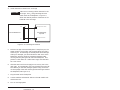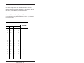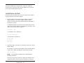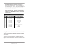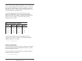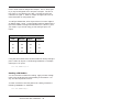
1
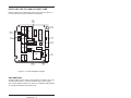
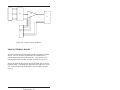
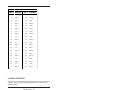
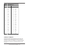
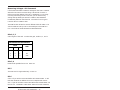
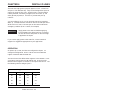
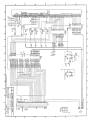
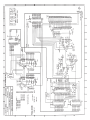
5700 User’s Manual Doc. #02798 Rev 1094 OCTAGON SYSTEMS CORPORATION® 6510 W. 91st Ave. Westminster, CO 80030 Tech. Support: 303–426–4521 COPYRIGHT Copyright 1991–94—Octagon Systems Corporation. All rights reserved. However, any part of this document may be reproduced, provided that Octagon Systems Corporation is cited as the source. The contents of this manual and the specifications herein may change without notice. TRADEMARKS Micro PC, PC SmartLink, Octagon Systems Corporation®, the Octagon logo and the Micro PC logo are trademarks of Octagon Systems Corporation. QuickBASIC® is a registered trademark of Microsoft Corporation. GW BASIC is a registered trademark of Microsoft Corporation. NOTICE TO USER The information contained in this manual is believed to be correct. However, Octagon assumes no responsibility for any of the circuits described herein, conveys no license under any patent or other right, and makes no representations that the circuits are free from patent infringement. Octagon makes no representation or warranty that such applications will be suitable for the use specified without further testing or modification. Octagon Systems Corporation general policy does not recommend the use of its products in life support applications where the failure or malfunction of a component may directly threaten life or injury. It is a Condition of Sale that the user of Octagon products in life support applications assumes all the risk of such use and indemnifies Octagon against all damage. IMPORTANT! Please read before installing your product. Octagon's products are designed to be high in performance while consuming very little power. In order to maintain this advantage, CMOS circuitry is used. CMOS chips have specific needs and some special requirements that the user must be aware of. Read the following to help avoid damage to your card from the use of CMOS chips. Using CMOS Circuitry – 1 Using CMOS Circuitry in Industrial Control Industrial computers originally used LSTTL circuits. Because many PC components are used in laptop computers, IC manufacturers are exclusively using CMOS technology. Both TTL and CMOS have failure mechanisms, but they are different. This section describes some of the common failures which are common to all manufacturers of CMOS equipment. However, much of the information has been put in the context of the Micro PC. Octagon has developed a reliable database of customer-induced, field failures. The average MTBF of Micro PC cards exceeds 11 years, yet there are failures. Most failures have been identified as customer-induced, but there is a small percentage that cannot be identified. As expected, virtually all the failures occur when bringing up the first system. On subsequent systems, the failure rate drops dramatically. ■ Approximately 20% of the returned cards are problem-free. These cards, typically, have the wrong jumper settings or the customer has problems with the software. This causes frustration for the customer and incurs a testing charge from Octagon. ■ Of the remaining 80% of the cards, 90% of these cards fail due to customer misuse and accident. Customers often cannot pinpoint the cause of the misuse. ■ Therefore, 72% of the returned cards are damaged through some type of misuse. Of the remaining 8%, Octagon is unable to determine the cause of the failure and repairs these cards at no charge if they are under warranty. The most common failures on CPU cards are over voltage of the power supply, static discharge, and damage to the serial and parallel ports. On expansion cards, the most common failures are static discharge, over voltage of inputs, over current of outputs, and misuse of the CMOS circuitry with regards to power supply sequencing. In the case of the video cards, the most common failure is to miswire the card to the flat panel display. Miswiring can damage both the card and an expensive display. ■ Multiple component failures - The chance of a random component failure is very rare since the average MTBF of an Octagon card is greater than 11 years. In a 7 year study, Using CMOS Circuitry – 2 Octagon has never found a single case where multiple IC failures were not caused by misuse or accident. It is very probable that multiple component failures indicate that they were user-induced. ■ Testing “dead” cards - For a card that is “completely nonfunctional”, there is a simple test to determine accidental over voltage, reverse voltage or other “forced” current situations. Unplug the card from the bus and remove all cables. Using an ordinary digital ohmmeter on the 2,000 ohm scale, measure the resistance between power and ground. Record this number. Reverse the ohmmeter leads and measure the resistance again. If the ratio of the resistances is 2:1 or greater, fault conditions most likely have occurred. A common cause is miswiring the power supply. ■ Improper power causes catastrophic failure - If a card has had reverse polarity or high voltage applied, replacing a failed component is not an adequate fix. Other components probably have been partially damaged or a failure mechanism has been induced. Therefore, a failure will probably occur in the future. For such cards, Octagon highly recommends that these cards be replaced. ■ Other over-voltage symptoms - In over-voltage situations, the programmable logic devices, EPROMs and CPU chips, usually fail in this order. The failed device may be hot to the touch. It is usually the case that only one IC will be overheated at a time. ■ Power sequencing - The major failure of I/O chips is caused by the external application of input voltage while the Micro PC power is off. If you apply 5V to the input of a TTL chip with the power off, nothing will happen. Applying a 5V input to a CMOS card will cause the current to flow through the input and out the 5V power pin. This current attempts to power up the card. Most inputs are rated at 25 mA maximum. When this is exceeded, the chip may be damaged. ■ Failure on power-up - Even when there is not enough current to destroy an input described above, the chip may be destroyed when the power to the card is applied. This is due to the fact that the input current biases the IC so that it acts as a forward biased diode on power-up. This type of failure is typical on serial interface chips. Using CMOS Circuitry – 3 ■ Serial and parallel - Customers sometimes connect the serial and printer devices to the Micro PC while the power is off. This can cause the failure mentioned in the above section, Failure upon power-up. Even if they are connected with the Micro PC on, there can be another failure mechanism. Some serial and printer devices do not share the same power (AC) grounding. The leakage can cause the serial or parallel signals to be 20-40V above the Micro PC ground, thus, damaging the ports as they are plugged in. This would not be a problem if the ground pin is connected first, but there is no guarantee of this. Damage to the printer port chip will cause the serial ports to fail as they share the same chip. ■ Hot insertion - Plugging cards into the card cage with the power on will usually not cause a problem. (Octagon urges that you do not do this!) However, the card may be damaged if the right sequence of pins contacts as the card is pushed into the socket. This usually damages bus driver chips and they may become hot when the power is applied. This is one of the most common failures of expansion cards. ■ Using desktop PC power supplies - Occasionally, a customer will use a regular desktop PC power supply when bringing up a system. Most of these are rated at 5V at 20A or more. Switching supplies usually require a 20% load to operate properly. This means 4A or more. Since a typical Micro PC system takes less than 2A, the supply does not regulate properly. Customers have reported that the output can drift up to 7V and/or with 7-8V voltage spikes. Unless a scope is connected, you may not see these transients. ■ Terminated backplanes - Some customers try to use Micro PC cards in backplanes that have resistor/capacitor termination networks. CMOS cards cannot be used with termination networks. Generally, the cards will function erratically or the bus drivers may fail due to excessive output currents. ■ Excessive signal lead lengths - Another source of failure that was identified years ago at Octagon was excessive lead lengths on digital inputs. Long leads act as an antenna to pick up noise. They can also act as unterminated transmission lines. When 5V is switch onto a line, it creates a transient waveform. Octagon has seen submicrosecond pulses of 8V or more. The solution is to place a capacitor, for example 0.1 µF, across the switch contact. This will also eliminate radio frequency and other high frequency pickup. Using CMOS Circuitry – 4 TABLE OF CONTENTS PREFACE ......................................................................... 1 Conventions Used in this Manual ..................................................... 1 Symbols and Terminology .................................................................. 2 Technical Support ............................................................................... 3 CHAPTER 1: OVERVIEW ............................................... 5 Description .......................................................................................... 5 Major Features .................................................................................... 5 CHAPTER 2: INSTALLATION ........................................ 7 Equipment ........................................................................................... 7 Installing the 5700 Analog Input Card ............................................. 8 Base Addresses ............................................................................ 8 Interrupt Source Lines ................................................................ 9 Interrupt Request Lines ............................................................ 10 DAC Output Voltage .................................................................. 10 Installing the 5700 in the Card Cage ....................................... 11 Troubleshooting ................................................................................. 13 Power Module ............................................................................. 13 Jumper Configurations .............................................................. 13 Where to Go From Here ................................................................... 13 CHAPTER 3: ANALOG INPUT ..................................... 15 Description ........................................................................................ 15 Analog Terminal board ..................................................................... 16 Control Register ................................................................................ 17 Auto Zero—Bit 0 ........................................................................ 18 Auto Calibration—Bit 1 ............................................................. 18 Gain Control—Bits 2 and 3 ....................................................... 19 Channel Select—Bits 4, 5, 6, and 7 .......................................... 20 Converting a Voltage ........................................................................ 21 Polling and Interrupts ...................................................................... 23 Polling ......................................................................................... 23 Interrupt ..................................................................................... 24 Programming Example ..................................................................... 24 Using the 5B Module Rack ............................................................... 30 Rack Control Lines .................................................................... 30 Connecting to a 5B Rack and Module ...................................... 31 i Reading a 5B Module ................................................................. 32 Writing to a 5B Module ............................................................. 33 CHAPTER 4: INPUT WITH CAMBASIC ....................... 35 Measuring Voltages .......................................................................... Analog Terminal Board .................................................................... CAMBASIC Commands .................................................................... Measuring Voltages: AIN Command ....................................... Bits 0, 1, 2 ................................................................................... Bits 3, 4 ....................................................................................... Bit 5 ............................................................................................. Bit 6 ............................................................................................. Bit 7 ............................................................................................. Using a 5B Module Rack .................................................................. Rack Control Lines .................................................................... Connecting to a 5B Rack and Module ...................................... Reading a 5B Module ................................................................. Writing to a 5B Module ............................................................. 35 35 36 37 37 37 37 37 38 38 39 39 40 41 CHAPTER 5: ANALOG OUTPUT ................................. 43 PC Control Cards .............................................................................. 43 Control Cards with CAMBASIC IV ................................................. 44 CHAPTER 6: DIGITAL I/O LINES ................................ 45 Operation ........................................................................................... 45 APPENDIX A: TECHNICAL DATA ............................... 47 Technical Specifications ................................................................... Jumper configurations ...................................................................... Connector Pinouts ............................................................................. Manual Calibration Procedures ....................................................... Zero Offset Adjustment ............................................................. Using QuickBASIC .................................................................... Using CAMBASIC IV ................................................................. Full Scale Voltage Adjustment ................................................. WARRANTY ii 47 48 51 53 53 54 54 54 PREFACE This manual is a guide to the proper configuration, installation, and operation of your 5700 Analog Input Card. Installation instructions, card mapping information and jumpering options are described in the main section of the manual; technical specifications and calibrations information are included in the appendix. The 5700 Analog Input expansion card is part of the Octagon Micro PC system. It is designed to be used with any other Micro PC Control Cards. You can use your 5700 card in conjunction with other Micro PC expansion cards, tailoring your system for a wide variety of applications. The 5700 card can also be used in an IBMcompatible PC. Micro PC cards are too tall to fit in an XT, but will fit in AT industrial size and other AT-size cases. All Micro PC products are modular, so creating a system is as easy as selecting and plugging in the products you need. CONVENTIONS USED IN THIS MANUAL 1. Information which appears on your screen (output from your system or commands or data that you key in) is shown in a different type face (note: the line breaks may not match those on your screen, but the message will be similar). Example 1: Octagon 5016 ROM BIOS Vers X.XX Copyright (c) 1990, Octagon Systems, Corp. All Rights Reserved Example 2: Press the <ESC> key. 2. Italicized refers to information that is specific to your particular system or program. For example: Enter filename means enter the name of your file. Names of other sections or manuals are also italicized. Preface – 1 3. Warnings always appear in this format: WARNING: The warning message appears here. 4. Paired angle brackets are used to indicate a specific key on your keyboard. For example, <ESC> means the escape key; <CTRL> means the control key; <F1> means the F1 function key. 5. All addresses are given in hexadecimal. SYMBOLS AND TERMINOLOGY Throughout this manual, the following symbols and terminology are used: W[ - ] Denotes a jumper block and the pins to connect. NOTE Information under this heading presents helpful tips for using the 5700 Card. Information under this heading warns you of situations which might cause catastrophic or irreversible damage. A/D Analog to Digital converter (or conversion). CAMBASIC IV An operating system and compiler designed specifically for control and data acquisition applications. DAC Digital to Analog converter (or conversion). H The suffix “H” denotes a hexadecimal number. For example, 1000H in hexadecimal equals 4096 in decimal. Preface – 2 Industrial Command Specialized CAMBASIC IV commands designed for industrial programming applications (e.g., AIN, AOT, BIT). PC Any personal computer with terminal emulation software, such as an IBM PC with PC SmartLINK. TTL Compatible Transistor-transistor-logic compatible; 0-5V logic levels. TECHNICAL SUPPORT If you have a question about the 5700 Analog Input expansion card and cannot find the answer in this manual, call Technical Support. They will be ready to give you the assistance you need. When you call, please have the following at hand: Your 5700 Analog Input Card User’s Manual A description of your problem The direct line to Technical Support is 303-426-4521. Preface – 3 This page intentionally left blank. Preface – 4 CHAPTER 1 OVERVIEW DESCRIPTION The 5700 Analog I/O Card coverts analog voltages to digital values (A/D) and digital values to analog voltages (DAC). Analog voltages are converted with 12 bit plus sign resolution from -FFFH (-4095 decimal) to +FFFH (+4095 decimal). Conversion time is 15 uS. The 16 single-ended analog input lines are multiplexed under software control. The gain amplifier, auto-zero, and auto-calibrate are also under software control. Inputs are protected from overload up to +/–15V even when power is off. The 5700 also has two 12-bit analog output channels, eight general purpose digital I/O lines, and an interface for a 5B module rack. The 5700 Analog I/O card measures 4.5 in. x 4.9 in. and uses one slot of the Micro PC card cage. MAJOR FEATURES Sixteen Analog Input Channels The 16 input lines are multiplexed under software control. Inputs are protected from overload up to +/–15V even when power is off. Input voltage range is +/–5V. Programmable Gain Amplifier The gain of each channel can be set to 1, 10, or 100, so each channel has its own full-scale value of +/–50 mV to +/–5V. Gain allows reading from a thermocouple and other low voltage sources. Sample and Hold Sample and hold capability is built into the 5700, allowing you to take a “snapshot” of the input. 50,000 Samples per Second The 5700 A/D converter can convert over 50,000 samples per second. Overview – 5 Eight Digital I/O Lines The 5700 has eight digital I/O lines which can be used for reading switches, connecting a keypad, and other general purpose control functions. These lines can be configured as inputs or outputs in groups of four lines. One line can be used to generate an interrupt. Two Analog Output Channels Each channel may have an output range of 0-5V, 0-10V, or +/–5V. The channels are written to independently. 5B Module Rack Interface The 5700 card connects to the 5B module rack with a CMA-26 cable. The 5B modules provide 1500V of isolation to analog inputs and outputs. Access Indicator An amber LED flashes briefly whenever the 5700 is accessed. This is useful when troubleshooting the card to know if a communications link has been established. Overview – 6 CHAPTER 2 INSTALLATION This chapter includes information on setting the base address, selecting the interrupt source and interrupt request line, selecting the DAC output voltage, and installing the 5700 Analog Input Card in the card cage. The 5700 is designed to be used with Octagon’s Micro PC system. It uses one card slot and plugs directly into the Micro PC backplane (motherboard). WARNING: The 5700 card contains static sensitive CMOS components. The greatest danger occurs when the card is plugged into a card cage. The 5700 card becomes charged by the user and the static discharges to the backplane from the pin closest to the card connector. If that pin happens to be an input pin, even TTL inputs may be damaged. To avoid damaging your card and its components: 1. 2. Ground yourself before handling the 5700 card. Disconnect power before removing or inserting the 5700 card. EQUIPMENT You will need the following equipment (or equivalent) to use your 5700: • • • • • 5700 Analog Input Card Micro PC Control Card Micro PC Card Cage Power Supply or Module PC SmartLINK and other software appropriate for your system You may also want to use: • 5B module and rack • CMA–26 cable • ATB–40 analog board • CMA–40 cable Installation – 7 INSTALLING THE 5700 ANALOG INPUT CARD Before installing the 5700 Analog Input Card, refer to Figure 2–1 for the location of various connectors and jumpers. DAC Voltage Source Access Indicator U12 Address Select R1 U8 U5 W1 U3 1 2 U1 IRQ W2 W4 U13 U9 12 IRQ Select 2 3 4 5 6 7 J1 Analog I/O 1 2 W3 U19 DAC Range U2 U20 1 2 U14 U10 Y1 R2 U21 W5 1 J4 J2 U4 5B Rack U15 U11 Interrupt Source Digital Port Figure 2–1—5700 Component Diagram Base Addresses The base address of the 5700 is configurable via jumpers and is set to 100H at the factory. If there is another card in your system with a base address of 100H, you must use a different base address (or change the address of the other card). Installation – 8 To change the base address, change the configuration of jumper block W1. Base Address Select Pins Jumpered Base Address [1-2][3-4][5-6] 100H* [3-4][5-6] 110H [1-2][5-6] 120H [5-6] 130H [1-2][3-4] 140H [3-4] 150H [1-2] 160H Not jumpered 170H * = default Interrupt Source Lines The 5700 card can be configured to use one of two interrupt sources if desired: one from the end of the conversion bit of the analog to digital converter, or one from the digital I/O line, port C, bit 0 (J4, pin 1). You can use only one source, which is selected by configuring jumper block W5. As shipped, the interrupt source is configured for the 82C55. However, the 5700 will function without an interrupt selected. Interrupt Request Lines: W5 Pins Jumpered Interrupt Source [1-2] A to D converter - End of Conversion [2-3]* 82C55A Port C, bit 0 (J4, pin 1) * = default Installation – 9 Interrupt Request Lines Jumper block W2 controls which line is used for the interrupt request. This line connects the interrupt signal from the source you select (with jumper block W5) to the control card. This line need not be set if no interrupt source is selected. Interrupt Request Lines: W2 Pins Jumpered Interrupt Request Line [1-2] IRQ 7 [3-4] IRQ 6 [5-6] IRQ 5 [7-8] IRQ 4 [9-10] IRQ 3 [11-12] IRQ 2 [9-11] No request line selected * * = default DAC Output Voltage Jumper block W3 and W4 select the output voltage for the analog output channels. The following table shows the jumper configurations and voltage levels for each channel. Default configuration is 0–5V output on the DACs. To change the voltage level, you must change the jumper settings of both W3 and W4. Each channel, 0 or 1, may be set to a different output range. Installation – 10 5700 DAC Output Voltage Output Range W3 W4 W3 W4 0-5V* [1-3] [3-5] [2-4] [4-6] 0-10V [7-9] [3-5] [8-10] [4-6] +/-5V [3-5] [1-3] [4-6] [2-4] Channel 0 Channel 1 * = default Installing the 5700 in the Card Cage The following instructions assume that you are using the 5B Module Rack and the ATB–40 Analog Board. If you are not using one or both of these, please disregard the steps describing their installation. 1. Turn card cage power off. 2. If you are using a 5B Module Rack, plug one end of the CMA– 26 cable into J2 on the 5700 Card. Plug the other end into the 26–pin socket on your 5B Module Rack (see Figure 2–2). 3. If you are using a ATB–40 Analog Terminal Board, plug one end of the CMA–40 into J1 on the 5700. Plug the other end into socket P1 on the ATB–40 Analog Board (see Figure 2–2). ATBÐ40 5700 CMA-40 5B Rack (SCMPB02) J1 J2 CMA-26 Figure 2–2—Positions of Sockets, Ribbon Cables, 5B Module Rack and ATB–40 Installation – 11 4. Install the 5700 in the Micro PC card cage. WARNING: Take care to correctly position the 5700 in the card cage. The Vcc and ground signals must match those on the backplane. Figure 2–3 shows the relative positions of the 5700 as it is installed in the card cage. A31 B31 Micro PC Motherboard Card Edge Pins A31 & B31 5700 12-Bit Analog Input Card A1 B1 Card Edge Pins A1 & B1 Figure 2–3—Card Edge Orientation 5. Position the cage so that the backplane is away from you, the power module is to the right, and the open side of the cage is closest to you. The lettering on the backplane should be right side up (for example, you should be able to read “A31” on the backplane), with the words OCTAGON SYSTEMS CORP. running vertically along the left side of the backplane. This position is “feet down” for a table mount cage, and “feet back” for a rear mount. 6. Slide the 5700 into the card cage (you can use any slot in the card cage). The components on the card should face to the left. The lettering on the card (Octagon Systems Corp.) should be on the top edge of the card and the gold contact fingers toward the backplane (see Figure 2–3). 7. Plug the 5700 into the backplane. 8. Connect modules and external devices to the 5B module rack and the ATB–40. 9. Turn on card cage power. Installation – 12 TROUBLESHOOTING If you have trouble getting your system to work properly, remove all cards except the Control Card and the 5700 Card from your system. Check the power module and jumpers. If you still encounter difficulties, please contact Technical Support at 303– 426–4521. Power Module Make sure the power cord is properly connected between the power module and the power source. Make sure the Control Card and 5700 are receiving power. The 5700 requires 5V +/–0.25V and 12V +/–0.6V when measured at the connector pins. The power module ripple should be less than 50 mV. Jumper Configurations The 5700 is shipped with jumper connections in place for Base I/O Address 100H, no interrupts selected, and a 0–5V output voltage selected. Jumper changes are usually not needed to get the system running. If you changed the jumpers and the system is not working properly, return the system to the original jumper positions. If the system still does not work, contact Technical Support. WHERE TO GO FROM HERE If you want to do this: Measure and Convert Analog Inputs — non–CAMBASIC systems, including ATB–40 Analog board, 5B Module Rack, auto–zero, and auto–calibrate. Turn to: Chapter 3 Measure and Convert Analog Inputs – CAMBASIC IV systems, including ATB–40 Analog board, 5B Module Rack, auto–zero, and auto–calibrate Chapter 4 Installation – 13 Analog Output for any Micro PC Control Card Chapter 5 On–card Digital I/O Lines Chapter 6 Manual Calibration Procedures Appendix A Installation – 14 CHAPTER 3 ANALOG INPUT DESCRIPTION You can connect equipment to the 5700 card with an ATB–40 analog terminal board, the 5B rack, or both. The 5700 can convert up to 16 input voltages to a digital value from 0 to 4095 counts plus a sign. You can measure voltages from –5.0V to +5.0V. Fastest conversion time is 15 uS. The 5700 card also has an amplifier to increase the voltage read from low output devices such as thermocouples and transducers by 10 or 100 times. The gain can be changed on the fly for each channel. The analog input has a sample and hold for the channel being sampled. The analog to digital (A/D) converter has auto–calibrate and auto– zero features. Auto–calibration adjusts positive linearity and full scale errors. Auto–zero corrects the zero error offset during every conversion. The 5700 card includes an interface to a 5B analog module rack. These modules are industry standard and have the capability of measuring thermocouples, strain gauges, voltage, and currents with up to 1500V of isolation. You can also control current output with a 5B module. This chapter includes information on setting the control registers to select a channel, setting the gain, and instructing the converter to auto–calibrate and auto–zero. The example program provided later in this chapter, shows how to read voltages, control the gain, auto–zero, auto–calibrate, and use the 5B module rack. Figure 3–1 shows functionally the system layout. Analog Input – 15 J1 MUX PGA A-D Control Register Figure 3–1—5700 Functional Schematic ANALOG TERMINAL BOARD The ATB–40 analog terminal board provides a connection for field wiring. You can use 12 to 22 gauge solid or stranded wire to connect equipment to the screw terminals. The ATB–40 is connected to the 5700 via a CMA–40 cable, as shown in Figure 2–2. The screw terminals bring the lines from the 5700 card out to the terminal board. Connection from the 5700 to the ATB–40 is one to one. There are 16 single–ended inputs and two optional outputs from J1. Analog Input – 16 5700 Analog Connector: J1 Pin # Function Pin # Function 1 In 0 21 In 10 2 AGnd 22 AGnd 3 In 1 23 In 11 4 AGnd 24 AGnd 5 In 2 25 In 12 6 AGnd 26 AGnd 7 In 3 27 In 13 8 AGnd 28 AGnd 9 In 4 29 In 14 10 AGnd 30 AGnd 11 In 5 31 In 15 12 AGnd 32 AGnd 13 In 6 33 Out 0 14 AGnd 34 AGnd 15 In 7 35 Out 1 16 AGnd 36 AGnd 17 In 8 37 +12V 18 AGnd 38 AGnd 19 In 9 39 -12V 20 AGnd 40 AGnd CONTROL REGISTER Functions are controlled by manipulating certain bits in the control register. The bit and corresponding functions are listed in the following table: Analog Input – 17 5700 Analog Input Control Register Bit Bit 0 Function 0 Auto zero On 1 Auto zero Off 0 Begin Auto Calibration 1 Auto Calibration Off The data to this register, which is a address BASE+4, is latched and will remain stable until written to again. Base is the address of the card as described in Chapter 2. Operation for each of the functions is described in the following sections: Auto Zero—Bit 0 When bit 0 is set low (0), the A/D converter will automatically compensate for any zero offset during each conversion. Performing an auto–zero doubles the time it takes to perform a conversion (to 29.2 uS). Setting bit 0 high (1) turns the auto–zero off. Auto zero is not the same as the manual calibration procedure. See Appendix A for using the zero adjust potentiometer. Auto Calibration—Bit 1 A calibration is performed automatically on power–up. Since the power supply reference and clock are not stable at power–up, this first calibration cycle will not result in an accurate calibration of the A/D. You should start a new calibration cycle after the system stabilizes. During calibration, correction values are determined for the offset voltage and any linearity and gain errors. These values are stored in internal RAM and used during an analog–to–digital conversion to bring the overall gain, offset, and linearity errors down to specified limits. Only one calibration cycle should be necessary after power–up, unless ambient conditions, such as temperature, change drastically. Auto–calibration is a separate, distinct function from any other conversion process. Auto–calibration is not part of the normal conversion process. Analog Input – 18 When bit 1 is set to 0, the A/D converter chip starts the calibration process. This process will take up to 760 uS. During calibration, no voltages may be converted. The status of calibration, like that of any conversion, is monitored at address BASE+1, bit 5. When bit 5 is low, a conversion is in process. During normal analog to digital conversion, bit 1 of the control register MUST be set to 1. To auto–calibrate: 1. Write to the control register with bit 1 set to 0. The value of the other bits isn’t critical, but should be set to the gain and an active channel (which channel doesn’t matter). Calibrating begins when bit 1 goes to 0. 2. Write to the control register with bit 1 set to 1. This bit must be set to 1 to convert any analog input. 3. Read the status of the conversion at BASE+1, bit 5. While this bit is low, calibration is in process. Calibration will take about 760 uS. 4. Analog to digital conversion can occur when the status of the conversion is high. Auto–calibrate is not the same as the manual calibration procedure. Manual calibration is described in Appendix A. Gain Control—Bits 2 and 3 Bits 2 and 3 control the gain. All analog inputs are brought to an amplifier with a gain of x1, x10, or x100. The output of the amplifier is then brought to the input of the A/D converter. 5700 Gain Control Bit 3 Bit 2 Gain 0 0 x1 0 1 x10 1 0 x100 Analog Input – 19 The setting time of the amplifier is 10 uS. For maximum accuracy, wait at least 10 uS after changing the gain or channels before initiating a conversion. Additional settling time may be necessary depending upon the impedance of your source. See the next section, Channel Select, for more information. Channel Select—Bits 4, 5, 6, and 7 One of 16 channels may be selected through bits 4–7, as shown in the following table: 5700 Channel Select Bit Channel 7 6 5 4 0 0 0 0 0 0 0 0 1 1 0 0 1 0 2 0 0 1 1 3 0 1 0 0 4 0 1 0 1 5 0 1 1 0 6 0 1 1 1 7 1 0 0 0 8 1 0 0 1 9 1 0 1 0 10 1 0 1 1 11 1 1 0 0 12 1 1 0 1 13 1 1 1 0 14 1 1 1 1 15 Analog Input – 20 The input impedance for any channel is more than 1 Mohms. Accuracy of any conversion will seriously degrade if any channel has an input voltage greater than 12V. CONVERTING A VOLTAGE Initiating an A/D conversion is a one or two step process, depending upon changes to the control register. 1. The first step is to write to the control register, located at address BASE+4. The control register selects the gain, channel, auto–zero and auto–calibrate functions (described in the previous section). If the BASE address of your 5700 Card is 100H and you want a gain of x1, convert channel 2 and perform an auto–zero. The value to write to the control register is: 00100010 = 22H In GW BASIC this is written as: 100 OUT &H104,&H22 In Z–80 code, it is written as: LD BC,104H LD A,22H OUT (C),A 2. The second step is to initiate a conversion by writing a 0 to the BASE address. For example, if you’re using GW BASIC and the BASE address of your card is 100H, you begin the conversion by writing: 110 OUT &H100,0 NOTE: C and assembly language users, please read the following precaution: The worst case accuracy scenario is when two channels, each at opposite polarity and at maximum voltage, are switched. Analog Input – 21 The program should delay at least 10 uS after switching channels before initiating a conversion. For example, if channel 2 was converted and had –5V on it and channel 3 is now selected and it has +5V on it, the program should delay 10 uS before starting a conversion. Starting a conversion any faster could result in inaccuracies. The converted value appears as 13 bits (12 bits plus sign), which is read as two bytes. The control card reads the least significant bits at address BASE and the most significant bits at address BASE+1. 5700 Data Format Bit Data at Base Address Data at Base +1 Address 0 Bit 0 of LSB Bit 8 of MSB 1 Bit 1 of LSB Bit 9 of MSB 2 Bit 2 of LSB Bit 10 of MSB 3 Bit 3 of LSB Bit 11 of MSB 4 Bit 4 of LSB Sign Bit 5 Bit 5 of LSB EOC (End of Conversion) 6 Bit 6 of LSB INT 7 Bit 7 of LSB Reserved The range is –4095 to +4095 counts. If the sign bit is 1, the voltage is negative. The End of Conversion (EOC) bit signals a conversion in progress when it is low. The INT bit is low when a conversion is complete. Reading the result or starting a conversation or calibration cycle set this output high. Analog Input – 22 POLLING AND INTERRUPTS You can either poll the converter to see when the conversion is complete or you can generate an interrupt when the conversion is complete. Polling is the simpler of the two procedures and is adequate for most applications. If you are using BASIC type programs (GW BASIC, QuickBASIC, etc.), the commands will take longer to execute than the time it takes to do a conversion, so it is unlikely you will ever get a “busy signal” from the converter. If you are using an assembly or C language, you may prefer to use an interrupt scheme. Normal conversion time is 14.6 uS without auto–zeroing and 29.2 uS with auto–zeroing. These short times may make an interrupt scheme unnecessary even with assembly language. Polling To poll, read the status of the EOC signal (bit 5 at address BASE+1). If bit 5=0, conversion is not complete. If bit 5+ 1, information is available and can be read by the control card. NOTE: Assembly or C language users, please note the following: The End of Conversion bit (at address BASE+1, bit 5) indicates when a conversion is complete. When low, a conversion is in progress. When high, a conversion is usually complete. The exception occurs immediately after initiating a conversion. If you want a conversion without auto–zero, the bit will be high for 3.5 uS after your start convert command is issued; then it will go low. If the conversion includes auto–zero, the bit will be high for 17 uS before going low. The bit will be low for approximately 14 uS before going high again. For auto calibration, this bit goes low virtually instantly after bit 0 goes low. The line will remain low until calibration is complete. You can write a program to monitor the line, detecting when the line goes low, then waiting for it to go high. However, if an interrupt happens while waiting for the line to go low, it is very likely that, after a return from Analog Input – 23 interrupt, the converter will be finished and the EOC bit will be high. There are several solutions to this problem. First, turn off all interrupts and follow the sequence above. Second, write a “do nothing” loop that will take approximately as long as a conversion will take before checking the EOC bit. Another alternative is to make the converter interrupt driven. The interrupt (INT) bit 6 at BASE+1 will go low when a conversion is complete. However, the INT line will immediately go high on any access to address BASE or BASE+1. Do not use this bit to determine an end of conversion. Interrupt Configure jumper block W5[1–2] so that the interrupt source is the A/D converter. Configure jumper block W2 for the desired interrupt request line to the control card. For example, W2[11–12] selects IRQ2. Make sure that the interrupt you select does not conflict with other interrupts on the bus. PROGRAMMING EXAMPLE The following programming example is written in QuickBASIC 3.0. It prompts the operator to select a channel, the gain, and whether to perform an auto–zero and/or auto–calibration. In addition, analog output and 5B module interface are also selected. More information on using the 5B module racks follows the programming example. ‘5700 analog input demonstration program ‘File name: 5700demo.bas ‘Date: 11–28–90 ‘Written using QuickBASIC V3.0 Analog Input – 24 ‘This program treats analog conversion as a subroutine called AIN. Variables called gain, channel, zero and can control the action of the converter. ‘The user may optionally output a voltage from the D–A converter to the channel of interest. Make sure to connect from J1–33 to J1–1. This connects the analog output to channel 0. ‘Define some variables used in this program. Undefined variables are single letter variables and are subject to change by any part of the program. start: BASE5700=&H100 controlw=0 gain=1 cal=1 zero=2 channel=0 'base address of 5700 'control word for A–D 'gain of amp. 'perform a calibration 'zero out converter 'channel number to convert print print"5700 Card demonstration program" print print"You will be asked a series of"; print"questions. Answer as prompted." print print"Enter channel number to convert"; Input"voltage (0–15):",channel print"Do you want to zero out the converter"; print"before conversion(Y or N)"; gosub getresp if y then zero = 0 'do a zeroing else zero = 1 'no zeroing end if print"Do you want to calibrate before"; print"conversion(Y or N)"; gosub getresp Analog Input – 25 If y then cal = 1 'calibrate else cal = 0 'no calibrate end if 'request gain Input "Enter 1,10, or 100 for gain";a gain = 99 'set to catch invalid input if a = 1 then gain = 0 'gain of 1 end if if a = 10 then gain = 4 end if 'gain of 10 If gain = 100 then 'gain of 100 gain = 8 end if If gain = 99 then beep print print"Wrong value entered!" print"Gain set to 1" gain = 0 end if print print"Do you want to output a voltage"; print"from P1–33?(Y or N)?"; gosub getresp if y then Input "Enter voltage";cv 'convert to binary units 'use 1.2207e–03 for 0–5 volts output cv = cv/1.2207e–03 'make into two bytes 'needed for DAC Analog Input – 26 msb lsb out out = cv\256 = cv mod 256 BASE5700+8,lsb BASE5700+0,msb 'update dacs out BASE5700+6,0 end if '5B rack query 'NOTE: All readings from the 5B rack use analog channel 15. This routine automatically sets the 5700 input channel to 15 if user wants to read from the 5B. 'force 5700’s 82C55 for port A & B for 'outputs, Port C is input out BASE5700+15,&H89 Print"Do you wish to read from the"; print"5B rack(Y or N) gosub getresp if y then input "5B rack channel number.";chno channel = 15 'force correct line 'output the channel to port B out BASE5700+13, chno end if 'see if want to output to the rack print"Do you wish to write to"; print"(output a voltage or current)"; print"the 5B rack(Y or N)"; gosub getresp if Y then Input "5B channel number.";chno 'Select the channel through port A out BASE5700+12,chno Analog Input – 27 print"Enter the voltage to the rack"; print"from 0 to 5V"; print"you wish to send to the" input"rack";cv 'convert voltage to a number 'the constant 1.2207e–03 assumes a 0–5 volt 'dac output. 'for other voltages, divide the maximum voltage 'into the maximum counts (10/4095 = 2.442e–03) cv = cv/1.2207e–03 msb = cv\256 lsb = cv mod 256 out BASE5700+10,lsb out BASE5700+11,msb 'update dacs out BASE5700+6,0 end if 'do the conversion and print out result gosub ain print"Returned print"volts." print value:";ainv*1.2207e–03; print"Do again(Y or N)"; gosub getresp if y then goto start end 'subroutine to perform A/D conversion ain: 'set up control word for this conversion controlw =2 'shut off calibration controlw = gain or zero or (channel*16) Analog Input – 28 'see if want to do a calibration 'of itself if cal = 1 then out BASE5700+4,controlw and &Hfd out BASE5700+4,controlw 'check if calibration complete 'this step is usually not needed for BASIC while(inp(BASE5700+1) and 32)<>32 wend end if 'send configuration to control register 'this sets the channel number, zero 'and gain options out BASE5700+4, controlw 'do the conversion out BASE5700,0 'This step is usually not necessary except 'for C and assembly language programs. 'Check to see if conversion is complete while (Inp(BASE5700+1) and 32)<>32 wend 'bring in the data lsb = inp(BASE7500) msb = inp(BASE5700+1) and 15 sign = inp(BASE5700+1) and 16 'convert the data into a binary number 'from 0 to 4095 'if number is negative, it will be a negative 'For example, –1000 could be a –f1.2 volts ' 1000 could be a positive 1.2 volts ainv = msb*256+lsb Analog Input – 29 if sign=16 then ainv=–(4095–ainv) end if 'done with conversion return 'get user response 'the variable y is returned true if 'the ‘y’ key is pressed getresp: input a$ if a$="y" or a$="Y" then y = –1 else y=0 end if return USING THE 5B MODULE RACK 5B modules are high performance, plug–in signal conditioners. They provide 1500V of isolation to analog inputs and outputs. You can measure voltage, current, and temperature with these modules. The modules plug into a rack, such as the SCMPB02. The modules are secured to the rack by a screw in the module. The rack connects to the 5700 Card via a CMA–26 cable. The outputs from the modules are multiplexed into one signal to the 5700 Card. Outputs are read on channel 15 on the 5700 Card. Each module is selected through a control line as described in the next section. Rack Control Lines An 82C55A chip on the 5700 provides the control lines for the SCMPB02 module rack. This chip has 24 programmable I/O lines. These are divided into three addressable ports of 8 bits each plus one control register. The control register is used to determine the Analog Input – 30 configuration of the 24 lines. Ports A and B are configured for outputs to select a module on the rack. Use port A to select an output module, such as a 5B39, on the rack. Use port B to select an input module, such as a 5B30. Select a module by writing a byte to one of these registers. The byte value, from 0 to 31, is an address that selects a corresponding position or channel on the rack. Bit position 6 low enables the selected module. Enable bit 6 of port A for writes; bit 6 of port B for reads. When you select an input module, the voltage from that module is connected to a common bus. This bus signal is connected to J2, pin 1 on the 5700 Card as analog input channel 15. When you select an output module, the amount of output is controlled by a voltage. The DC voltage comes from the 5700 Card through J2, pin 3. The voltage then goes to a bus on the 5B rack. The selected module reads this voltage and converts its level to the corresponding output. Figure 2–2 shows the interconnection between the 5700, 5B rack, and a module for reading and writing a module. Connecting to a 5B Rack and Module Connect a CMA–26 ribbon cable from J2 on the 5700 Card to the 26 pin connector on the 5B rack. Racks can be configured for addresses 0–15 or 16–31. Be sure to configure the rack for the following examples as a stand alone unit, which is address 0–15. Connect +5 and ground to the appropriate screw terminals on the 5B rack. Plug the 5B modules into any slot on the rack. The examples that follow use the third slot, which is address 2. The 82C55A chip on the 5700 Card must be configured before using a 5B rack. The examples that follow are expressed as an address from the 5700 Card BASE address. Analog Input – 31 Ports A and B must be configured as outputs. Port C, which goes to J4, may be configured as 4 or 8 inputs or outputs. The first 4 bits of port C are referred to as Lower C and the last 4 bits are referred to as Upper C. Refer to Chapter 6, Digital I/O Lines, for more information on using these lines. To configure the 82C55A, write a byte value to its control register at address BASE + OFH. Use the following table to determine the byte value needed to configure the 82C55A Port C (which is J4) to your needs. If you are not using J4, then configure port C for inputs. 5700 Control Register Command Hex Decimal Upper C Lower C 80 128 Out Out 81 129 Out In 88 136 In Out 89 137 In In Using the control words from the above table will always configure ports A and B as outputs. The following GW BASIC example makes port C all inputs: 100 OUT BASE+15,137 Reading a 5B Module You can now select a module for reading. Apply a known voltage input to screw terminals corresponding to the module. Usually, this will be positions 2 and 3. To select a module in the third position for reading, execute the following GW BASIC statement: 110 OUT BASE+&HOD,2 Analog Input – 32 The number 2 may be substituted for the desired 5B channel number. Note that since bit 6 of the output word is low, the read line to the 5B rack is enabled, allowing you to read the voltage from analog channel 15 with a gain of 1. Autozero may be ON or OFF. To read the voltage from the 5B rack with any autozero, execute the following GW BASIC statements: 'Control port= Channel 15, gain =1, autozero OUT BASE+0,0 'This starts the A/D conversion WHILE INP((BASE+1)AND A32) 'Busy check– probably not WEND 'necessary LSB=INP(BASE) 'Get low byte MSB=INP(BASE+1) AND 15 'Get high byte SN=INP(BASE+1) AND 16 'Negative number? AINV=MSB*256+LSB 'Convert to 16 bit number IF SN THEN AINV+–(4095–AINV) 'Negative if sign bit set 120 OUT BASE+4,&HF2 130 140 150 160 170 180 190 200 AINV now contains the reading from the selected 5B module. To turn off a module, set bit 6 of the address word high. The following example turns off ALL the 5B modules for reading: 210 OUTBASE+13,&H40 'Set bit 6 high Writing to a 5B Module The amount of output from a 5B module will vary according to the control voltage applied to it. A control voltage is supplied to the 5B rack bus from the 5700 Card by controlling an on–card DAC (U20). The output of DAC1 goes to J2, pin 3 and to J1, pin 35. DAC0 and DAC1 are also described in Chapter 5. The output of DAC1 must be jumpered for 0–5V output, which is jumper configuration W3[2–4] and W4[4–6]. You must set the output voltage from DAC1 before writing to the 5B module. The desired output voltage is generated by following Analog Input – 33 the following example steps (written in GW BASIC): 200 210 220 230 240 250 260 'Convert desired voltages to counts CV = CV/1.2207E–03 MSB = CV\256 'make MSB of word LSB = CV Mod 256 'make LSB of word OUT BASE+10,LSB OUT BASE+11,MSB OUT BASE+6,0 'update DACs This example takes the desired voltage (from 0–5V) into variable CV. The variable CV is converted into the number of counts needed to produce a voltage. Lines 220 and 230 make most and least significant bytes for the DAC. Line 260 updates the value to the DAC. Selecting the 5B output module is similar to selecting the input modules, except the address is BASE+12. If the 5B output module is in channel 5, the following GW BASIC example will select this module: 270 OUT BASE+12,5 To de–select all output modules (i.e., turn outputs off), set bit 6 high, for example: 280 OUT BASE+12,&49 When using 5B output modules, the modules must be continuously updated in your program. You can use multiple 5B output modules in a rack. The modules are usually 2 to 5 mS. You must do the updating in your program. The modules are usually scanned at the same time. Scanning output modules does not affect input modules and vice versa. Analog Input – 34 CHAPTER 4 INPUT WITH CAMBASIC MEASURING VOLTAGES You can connect equipment to the 5700 using an ATB–40, 5B rack or both. Up to 16 inputs may be converted to a digital value from 0 to 4095 or any “real” number. You can measure voltages from –5.0V to +5.0V. The 5700 has an amplifier to increase the voltage read from low output devices such as thermocouples and transducers by 10 or 100 times. The gain can be changed for each channel every time an AIN is performed. Conversion takes approximately 1 mS. The analog to digital converter (A/D) has auto–calibrate and auto– zero features. Auto–calibration adjusts positive linearity, full scale errors, and zero. Auto–zero corrects the zero error during every conversion. The 5700 card includes an interface to a 5B analog module rack. These modules are industry standard and have the capability of measuring thermocouples, strain gages, voltage, and current output with a 5B module. This chapter includes information on using the 5700 card with Micro PC Control Cards with CAMBASIC IV (for example, the 5080 Control Card). ANALOG TERMINAL BOARD The ATB–40 analog terminal board provides a connection for field wiring. You can use 12 to 22 gauge solid or stranded wires to connect equipment to the screw terminals. The ATB–40 is connected to the 5700 via a CMA–40 ribbon cable, as shown in Figure 2–2. The screw terminals essentially bring the lines from the 5700 card out to the terminal board. Wiring from the 5700 to the ATB–40 is one to one. There are 16 single–ended inputs and two optional outputs from J1. The following table shows pin numbers and the corresponding inputs and outputs. Analog Input with CAMBASIC – 35 5700 Analog Connector: J1 Pin # Function Pin # Function 1 In 0 21 In 10 2 AGnd 22 AGnd 3 In 1 23 In 11 4 AGnd 24 AGnd 5 In 2 25 In 12 6 AGnd 26 AGnd 7 In 3 27 In 13 8 AGnd 28 AGnd 9 In 4 29 In 14 10 AGnd 30 AGnd 11 In 5 31 In 15 12 AGnd 32 AGnd 13 In 6 33 Out 0 14 AGnd 34 AGnd 15 In 7 35 Out 1 16 AGnd 36 AGnd 17 In 8 37 +12V 18 AGnd 38 AGnd 19 In 9 39 -12V 20 AGnd 40 AGnd CAMBASIC COMMANDS The AIN and CONFIG AIN commands are used to return the analog input value. More detailed information on using the commands is located in the CAMBASIC IV Programming Guide. Please refer to this manual for complete descriptions of these commands. Analog Input with CAMBASIC – 36 Measuring Voltages: AIN Command Use the AIN command to measure voltages on the 5700. CONFIG AIN tells the Control Card two things: What kind of card it is talking to and the address of the card. CAMBASIC IV can recognize only one analog card at a time, but you can install many analog cards provided you execute a CONFIG AIN statement immediately before an AIN function. The kind of card is type 0. Use this value in CONFIG AIN. The AIN function allows for several different kinds of modes. The various modes are set by a bit in the mode byte in the AIN function. The kinds of modes allowed are described below. Bits 0, 1, 2 Sets the gain of the card. To select the gain, set bits 0, 1, and 2. AIN Command and Gain Selection Bit # Gain 2 1 0 0 0 0 x1 0 0 1 x10 0 1 0 x100 Bits 3, 4 Reserved for possible future use. Enter 0’s. Bit 5 The 5700 card is single ended only. Enter a 0. Bit 6 Set to 1 if you wish to auto–zero before each measurement. It will take the converter an additional 15 uS to complete each conversion. If you do not want to auto–zero before each measurement, set this bit to 0. CAMBASIC takes about 1000 uS for each statement, Analog Input with CAMBASIC – 37 so the extra 15 uS required for an autozero will not degrade performance at all. When using BASIC, an autozero is recommended. Bit 7 Set this bit to 1 if you want the A/D to auto–calibrate. This will require 750 uS to do an auto–calibration cycle. Normally, auto– calibration is performed only once after power up. Set this bit to 0 to disable auto–calibration. Perform an auto–calibration periodically, as deemed necessary, due to changing ambient conditions. The following program example initializes CAMBASIC IV for a 5700 Card at address 100H. An analog voltage from channel 3 is returned. Gain is set to x1 and an auto–zero will be performed. 100 CONFIG AIN 0,&100 110 A=AIN(3,@10000000,0) Refer to the CAMBASIC IV Programming Guide for further information. The input impedance of any channel is more than 1 Mohm. The conversion accuracy of any channel will seriously degrade if the input voltage to any channel is greater than 12V. USING A 5B MODULE RACK 5B modules are high performance, plug–in signal conditioners. They provide 1500V of isolation to analog inputs. You can measure voltage, current, and temperature with these modules. Modules plug into a rack, such as the SCMPB02. The modules are secured to the rack by a screw in the modules. This rack connects to the 5700 Card via a CMA–26 cable. The outputs from the modules are multiplexed into one signal to the 5700 Card. Outputs from the modules are read on channel 15 on the 5700 Card. Each module is selected through a control line as described in the next section. Analog Input with CAMBASIC – 38 Rack Control Lines An 82C55A chip provides the control lines for the SCMPB02 module rack. This chip has 24 programmable I/O lines. These are divided into three addressable ports of 8 bits each plus one control register. The control register is used to determine the configuration of the 24 lines. Ports A and B are configured for outputs to select a module on the rack. Use port A to select an output module, such as a 5B39, on the rack. Use port B to select an input module, such as as 5B30. Select a module by writing a byte to one of these registers. The byte value, from 0 to 31, is an address that selects a corresponding position or channel on the rack. Bit position 6 allows a read from the selected module (Port B) or a write to a module (Port A). When you select an input module, the voltage from that module goes on to a common bus. This bus signal goes to J2, pin 1 on the 5700 Card as an analog input channel 15. When you select an output module, the amount of output is controlled by a voltage. The DC voltage comes from the 5700 Card through J2, pin 3. The voltage then goes to a bus on the 5B rack. The selcted module reads this voltage and converts its level to the corresponding output. Connecting to a 5B Rack and Module Connect a CMA–26 ribbon cable from J2 on the 5700 Card to the 26 pin connector on the 5B rack. Racks can be configured for addresses 0–15 or 16–31. Be sure to configure the rack for the following examples as a stand alone unit, which is address 0–15. Connect +5 and ground to the appropriate screw terminals on the 5B rack. Plug the 5B modules into any slot on the rack. The examples that follow use the third slot, which is address 2. The 82C55A chip on the 5700 Card must be configured before using a 5B rack. The examples that follow are expressed as an address from the 5700 BASE. Analog Input with CAMBASIC – 39 Ports A and B must be configured as outputs. Port C, which goes to J4, may be configured as 4 or 8 inputs or outputs. The first 4 bits of port C are referred to as Lower C and the last 4 bits are referred to as Upper C. Refer to Chapter 6, Digital I/O Lines, for more information on using these lines. To configure the 82C55A, write a byte value to its control register at address BASE + OFH. Use the following table to determine the byte value needed to configure the 82C55A Port C (which is J4) to your needs. If you are not using J4, then configure port C for inputs. 5700 Control Register Command Hex Decimal Upper C Lower C 80 128 Out Out 81 129 Out In 88 136 In Out 89 137 In In Using the control words from the above table will always configure ports A and B as outputs. The following CAMBASIC IV example makes port C all inputs: 100 OUT BASE+15,137 Reading a 5B Module You can now select a module for reading. Apply a known voltage input to the screw terminals corresponding to the module. Usually, this will be positions 2 and 3. To select a module in the third position for reading, execute the following CAMBASIC IV statement: 100 OUT BASE+&OD,2 Analog Input with CAMBASIC – 40 The number 2 may be substituted for the desired 5B module number. Note that since bit 6 of the output word is low, the read line to the 5B rack is enabled, allowing you to read the voltage from analog channel 15 with a gain of 1. Autozero may be ON or OFF. To read the voltage from the selected 5B module with an autozero, execute the following CAMBASIC IV statement: 120 A=AIN(15,@010000000,0) autozero 'channel 15, gain=1, “A” now contains the reading from the selected 5B module. To turn off a module, set bit 6 of the address word high. The following example disables ALL the 5B modules for reading: 210 OUT BASE+13&40 'Set bit 6 high Writing to a 5B Module The amount of output from a 5B module will very according to the control voltage applied to it. A control voltage is supplied to the 5B rack bus from the 5700 card by controlling the on–card DAC (U20). The output of DAC1 is connected to J2, pin 3, the 5B rack write bus. DAC0 and DAC1 are also described in Chapter 5. The output of DAC1 must be jumpered for a 0–5V output, which is jumper configuration W3[2–4] and W[4–6]. You must set the output voltage from DAC1 before writing to the 5B module. Execute the following CAMBASIC IV statements to generate the voltage on DAC1: 200 counts 210 CV=CV/1.2207E–03 220 AOT(1,CV) 'Convert desired voltage to '5V/4096 'Send the counts to DAC1 Note that a CONFIG AOT statement must have been executed before this example will run. See Chapter 5 for details. Analog Input with CAMBASIC – 41 Selecting the 5B output module is similar to selecting the input modules, except the address is BASE+12. The following CAMBASIC IV example will select 5B output module in position 5: 230 OUT BASE+12,5 To turn off a module, set bit 6 of the address word high. The following example disables ALL the 5B modules for writing: 210 OUT BASE+12,&40 'Set big 6 high When using 5B output modules, the modules must be continuously updated, or ‘refreshed’ in order for them to maintain their output. The update time is usually 2 to 5 mS. You must write your program so that all output modules are refreshed every 5 mS or sooner. Analog Input with CAMBASIC – 42 CHAPTER 5 ANALOG OUTPUT The 5700 card has two 12–bit digital to analog (DAC) output channels. Each channel can have a range of 0–10V, 0–5V, or +/–5.0V. The range is determined by the configuration of jumper blocks W3 and W4. 5700 DAC Output Voltage Output Range W3 W4 W3 W4 0-5V* [1-3] [3-5] [2-4] [4-6] 0-10V [7-9] [3-5] [8-10] [4-6] +/-5V [3-5] [1-3] [4-6] [2-4] Channel 0 Channel 1 * = default The outputs from both channels go to J1. DAC0 output is J1, pin 33 and DAC1 output is J1, pin 35. Corresponding grounds are J1, pin 34 and J1, pin 36, although any even numbered pin may be used for ground. PC CONTROL CARDS To send an analog value to one of the DAC ports, write the LSB and MSB to the appropriate channel. The order is not important. The output will not change until a write to BASE+6 occurs. In this way, you can write to both channels and simultaneously update the outputs. The following example, written in GW BASIC, shows how to change the outputs of both DACs. V0 is the desired output voltage from DAC0 and VI is the desired output from DAC1. DAC0 is jumpered for a voltage range of 0–10V and DAC1 is set for 0–5V. 100 110 120 140 150 160 'Convert volts to bits in D0,D1 D0 = VO/2.442E–03 D1 = V1/1.2207E–03130 'make up bytes for DAC0 MSB + D0\256 LSB = D0 MOD 256 OUT BASE+8, LSB Analog Output – 43 170 180 190 200 220 225 230 240 OUT BASE+9, MSB 'make up bytes of DAC1 MSB = INT(D1/256) LSB = D0–MSB*256 OUT BASE+10,LSB OUT BASE+11, MSB 'update both dacs OUT BASE+6,0 Both DACs may, but do not have to, be updated at the same time. Changing one DAC will not affect the other and the update statement at line 240 will not change its output. CONTROL CARDS WITH CAMBASIC IV CAMBASIC IV uses CONFIG AOT to configure the analog output. The type parameter is 0 for the 5700 Card. CAMBASIC IV software can store only one type of analog card in its memory at a time. If another 5700 Card or analog output card is in the card cage, you must execute a separate CONFIG AOT immediately before the AOT command. The AOT command writes data to one of the two analog output ports. Allowable channel numbers are 0 and 1. Allowable values are from 0 to 4095. The following program example tells CAMBASIC IV that there is a 5700 Card at address 100H. A binary count value of 2000 is sent out for channel 0 and 3000 for channel 1. 100 CONFIG AOT 0,&100 110 AOT 0,2000 120 AOT 1,3000 Analog Output – 44 CHAPTER 6 DIGITAL I/O LINES The 5700 has eight general purpose digital I/O lines. These lines are port C of an 82C55A chip. They can be configured as inputs or outputs in groups of four lines. These lines at J4 can be used for reading switches, connecting a keypad (such as the KP–1), and other general purpose I/O. All lines at J4 have 10K pull–up resistors. You can configure J4, pin 1 as an interrupt source by jumpering W5[2–3]. The A/D converter cannot be used as an interrupt source when this line is used. The interrupt can be used to indicate an emergency condition (from a switch, for example). Apply power to the 5700 card before applying input voltages to the digital I/O lines. Excessive current will flow if 5700 power is off and voltage is applied to the inputs. WARNING: If you cannot apply power to the 5700 first, contact Technical Support for suggestions appropriate to your application. OPERATION On power–up or reset, the lines are configured as inputs. To change the configuration, write a control word to the 82C55A register located at address BASE+15. The control word also affects other registers in the 82C55A. Ports A and B are used to control a 5B module rack. Every time the 82C55A control register is written to, the outputs are set to 0. Use the following table to configure port C. 5700 Control Register Command Hex Decimal Upper C Lower C 80 128 Out Out 81 129 Out In 88 136 In Out 89 137 In In Digital I/O Lines – 45 The following example, written in QuickBASIC, configures port C for all outputs. The 5700 card is assumed to be at address 100H. OUT &H10F,128 In CAMBASIC IV, the program would read: 100 OUT &10F,128 When a line is configured as an output, it can sink a maximum of 2.5 mA at 0.4V and can source over 2.5 mA at 2.4V. To read the status of a port, use the INP statement: in QuickBASIC: A=INP(&H10E) In CAMBASIC IV: A=INP(&10E) 'Reads Port C of 82C55A 'Reads Port C of 82C55A Refer to Appendix A, “Technical Specifications”, for J4 pinout. Digital I/O Lines – 46 APPENDIX A TECHNICAL DATA TECHNICAL SPECIFICATIONS Power specifications 5V at 50 mA (typical), +/–12V at 20 mA Evnironmental specifications –40o to 85° C operating RH 5% to 95%, noncondensing Input Impedance Greater than 1 Mohm Maximum Input Voltage Input Power OFF +/–12V Power ON* +/–12V *Accuracy of converted readings will be affected when any channel exceeds 12V. A/D Accuracy x1 gain +/–4 counts x10 gain +/–6 counts x100 gain +/–8 counts +/–12 counts for a selected range D/A Ranges 0–5V, 0–10V, +/–5V Maximum Output Current 5 mA Digital I/O Port 8 lines configurable as inputs or outputs, in groups of 4. Outputs are TTL compatible. Driver Current 2.5 mA maximum, sink or source Bus Compatibility Full IBM PC, 8 MHz I/O Bus Mechanical Specification 4.5 in x 4.9 in. Technical Data – 47 JUMPER CONFIGURATIONS W1: Base Address The base accress of the 5700 card is configurable via jumpers and is set to 100H at the factory. Base Address Select Pins Jumpered Base Address [1-2][3-4][5-6] 100H* [3-4][5-6] 110H [1-2][5-6] 120H [5-6] 130H [1-2][3-4] 140H [3-4] 150H [1-2] 160H Not jumpered 170H * = default W2: Interrupt Request Line Jumper block W2 controls which line is used for the interrupt request. Technical Data – 48 Interrupt Request Lines: W2 Pins Jumpered Interrupt Request Line [1-2] IRQ 7 [3-4] IRQ 6 [5-6] IRQ 5 [7-8] IRQ 4 [9-10] IRQ 3 [11-12] IRQ 2 [9-11] No request line selected * * = default W3 and W4: DAC Output Voltage Jumper blocks W3 and W4 select the output voltage for the analog output channels. Default configuration is 0–5V output on the DACs, which is configuration W3[1–3,2–4]W4[3–5,4–6]. To change the voltage level, you must change the jumper settings for both W3 and W4. Each channel, 0 or 1, may be set to a different output range. 5700 DAC Output Voltage Output Range W3 W4 W3 W4 0-5V* [1-3] [3-5] [2-4] [4-6] 0-10V [7-9] [3-5] [8-10] [4-6] +/-5V [3-5] [1-3] [4-6] [2-4] Channel 0 Channel 1 * = default W5: Interrupt Source Lines You can use only one source, which is selected by configuring jumper block W5. As shipped, the A/D converter is jumpered [1–2] to provide the interrupt source. However, no interrupt request line is selected at W2. Technical Data – 49 Interrupt Request Lines: W5 Pins Jumpered Interrupt Source [1-2] A to D converter - End of Conversion [2-3]* 82C55A Port C, bit 0 (J4, pin 1) * = default Technical Data – 50 CONNECTOR PINOUTS 5700 Analog Connector: J1 Pin # Function Pin # Function 1 In 0 21 In 10 2 AGnd 22 AGnd 3 In 1 23 In 11 4 AGnd 24 AGnd 5 In 2 25 In 12 6 AGnd 26 AGnd 7 In 3 27 In 13 8 AGnd 28 AGnd 9 In 4 29 In 14 10 AGnd 30 AGnd 11 In 5 31 In 15 12 AGnd 32 AGnd 13 In 6 33 Out 0 14 AGnd 34 AGnd 15 In 7 35 Out 1 16 AGnd 36 AGnd 17 In 8 37 +12V 18 AGnd 38 AGnd 19 In 9 39 -12V 20 AGnd 40 AGnd Technical Data – 51 5700 Analog I/O Backpanel: J2 Pin # Function Pin # Function 1 VRD 14 W1 2 IO COM 15 W2 3 VWR 16 W3 4 NC 17 W4 5 IO COM 18 W5 6 O COM 19 REN* 7 R0 20 WEN* 8 R1 21 NC 9 R2 22 Reserved 10 R3 23 NC 11 R4 24 NC 12 R5 25 D COM 13 W0 26 D COM * = Write enable low Technical Data – 52 5700 Digital I/O Connector: J4 Pin # Function 1 I/O 0, INT 2 I/O 6 3 I/O 5 4 I/O 1 5 I/O 2 6 I/O 4 7 I/O 7 8 I/O 3 9 NC Gnd 10 MANUAL CALIBRATION PROCEDURES NOTE: A digital voltmeter (DVM) capable of .02% accuracy must be used to properly perform these procedures. Zero Offset Adjustment The programmable gain amplifier used in the 5700 may have some offset and can be nulled (zeroed) by the adjusting potentiometer R1. The amplifier offset is amplified by the selected gain. If you intend to leave the gain at one setting continuously, the amplifier should be nulled at that gain. If gains are to be switched, it is recommended that the offset be nulled at the x100 gain setting. This will give better overall performance than nulling at x1 and then reading at x100. Attach the negative (–) lead of the DVM to the analog ground (any even pin on connector J1). Attach the positive (+) lead of the DVM to the output of the programmable gain amplifier, either pin 15 of U3, the cathode of CR5, or the anode of CR4. Short input channel 0 to analog ground. A two pin shorting jumper between pins 1 and 2 connector J1 works well for this. Technical Data – 53 Using QuickBASIC Run one of the following program lines, depending on which gain you wish to use. out&h104,2 out&h104,6 out&h104,&h0a 'channel 0, gain=1 'channel 0, gain=10 'channel 0, gain=100 Using CAMBASIC IV Run one of the following program lines, depending on which gain you wish to use: 10 OUT &104,2 20 OUT &104,6 30 OUT &104,&A 'channel 0, gain=1 'channel 0, gain=10 'channel 0, gain=100 Adjust potentiometer R1 until the DVM reads 0V. Full Scale Voltage Adjustment The reference voltage for the A/D converter is adjustable via potentiometer R2. This voltage can be set for 5V full scale. This gives 1.2207 mV/count, or +4096 counts for a 5V input. Place the negative (–) lead of the DVM on analog ground (any even pin of connector J1). Place the positive (+) lead of the DVM to the reference voltage for the A/D, pin 2 or 4 of U5, or the cathode of CR4. Adjust potentiometer R2 until the DVM reads 5V. This completes the zero and full scale adjustments. Technical Data – 54 WARRANTY Octagon Systems Corporation (Octagon), warrants that its standard hardware products will be free from defects in materials and workmanship under normal use and service for the current established warranty period. Octagon’s obligation under this warranty shall not arise until Buyer returns the defective product, freight prepaid to Octagon’s facility or another specified location. Octagon’s only responsibility under this warranty is, at its option, to replace or repair, free of charge, any defective component part of such products. LIMITATIONS ON WARRANTY The warranty set forth above does not extend to and shall not apply to: 1. 2. 3. Products, including software, which have been repaired or altered by other than Octagon personnel, unless Buyer has properly altered or repaired the products in accordance with procedures previously approved in writing by Octagon. Products which have been subject to power supply reversal, misuse, neglect, accident, or improper installation. The design, capability, capacity, or suitability for use of the Software. Software is licensed on an “AS IS” basis without warranty. The warranty and remedies set forth above are in lieu of all other warranties expressed or implied, oral or written, either in fact or by operation of law, statutory or otherwise, including warranties of merchantability and fitness for a particular purpose, which Octagon specifically disclaims. Octagon neither assumes nor authorizes any other liability in connection with the sale, installation or use of its products. Octagon shall have no liability for incidental or consequential damages of any kind arising out of the sale, delay in delivery, installation, or use of its products. SERVICE POLICY 1. 2. 3. Octagon’s goal is to ship your product within 5 working days of receipt. If a product should fail during the warranty period, it will be repaired free of charge. For out of warranty repairs, the customer will be invoiced for repair charges at current standard labor and materials rates. Customers that return products for repairs, within the warranty period, and the product is found to be free of defect, may be liable for the minimum current repair charge. RETURNING A PRODUCT FOR REPAIR Upon determining that repair services are required, the customer must: 1. 2. 3. 4. 5. 6. 7. Obtain an RMA (Return Material Authorization) number from the Customer Service Department, 303-430–1500. If the request is for an out of warranty repair, a purchase order number or other acceptable information must be supplied by the customer. Include a list of problems encountered along with your name, address, telephone, and RMA number. Carefully package the product in an antistatic bag. (Failure to package in antistatic material will VOID all warranties.) Then package in a safe container for shipping. Write RMA number on the outside of the box. For products under warranty, the customer pays for shipping to Octagon. Octagon pays for shipping back to customer. Other conditions and limitations may apply to international shipments. NOTE: PRODUCTS RETURNED TO OCTAGON FREIGHT COLLECT OR WITHOUT AN RMA NUMBER CANNOT BE ACCEPTED AND WILL BE RETURNED FREIGHT COLLECT. RETURNS There will be a 15% restocking charge on returned product that is unopened and unused, if Octagon accepts such a return. Returns will not be accepted 30 days after purchase. Opened and/or used products, non-standard products, software and printed materials are not returnable without prior written agreement. GOVERNING LAW This agreement is made in, governed by and shall be construed in accordance with the laws of the State of Colorado. The information in this manual is provided for reference only. Octagon does not assume any liability arising out of the application or use of the information or products described in this manual. This manual may contain or reference information and products protected by copyrights or patents. No license is conveyed under the rights of Octagon or others.