1
RESEARCH ACTIVITY REPORT
Development of fast controls for beam wire scanner at SuperKEKB
Anindya Roy (VECC, DAE, India)
July 4, 2012
Objective:
The KEK 8-GeV LINAC injects electron e- and positron e+ beams with different characteristics
into four storage rings: KEKB high-energy ring (HER), KEKB low-energy ring (LER), Photon Factory
(PF) and PF-AR. The wire scanners are used to monitor beam profile non-destructively along the beam
line. Again a set of three wire scanners are used to calculate beam emittance and Twiss parameter for
optics matching in LINAC & BT. The principle objective is to develop an event based data acquisition
system, synchronised with LINAC timing system, for acquiring multiple beam mode data simultaneously.
Introduction:
In LINAC, a optics matching system consists of a set of four pulse motor based wire movement
mechanism, photo-multiplier tubes (PMT), high voltage power supplies and a data acquisition system. At
present, the data acquisition system is comprised of CAMAC based ADC, Scaler and DAC modules. A
supervisory EPICS IOC, VME based, is used to control wire movement, high voltage and also to acquire
data from CAMAC hardware. The configuration of the present system is described in details in the next
section. The main disadvantage of the system is that, the data acquisition process is not synchronized with
the LINAC timing system and hence unable to acquire multimode beam data simultaneously. Since
LINAC is used for simultaneous top-up injections to three rings, KEKB-HER, KEKB-LER, and PF,
therefore a data acquisition system, which utilizes timing events for data acquisition, will be useful for
acquiring multiple beam mode data simultaneously.
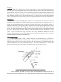
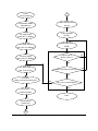
Wire scanner system:
A wire scanner system is used to measure the beam size non-destructively. It consists of a
tungsten wire of 100!m diameter wound on frame to form X, Y and U wire perpendicular to beam. A
pulse motor drive system is used to move the frame into the beam pipe in a controlled manner. The
system is installed in such a way so that, the wires, X, Y and U, scan the beam in X, Y and U (45°)
direction while moving into the beam pipe. The schematic of the system is shown in Fig 1.
Fig. 1: Schematic of wire scanner system
A photo multiplier tube (PMT) is used to collect the Bremsstruhlung radiation emitted due to
interaction of the beam with the wires. The output of the PMT is integrated using a charge integral type
ADC. A pulse motor controller with GPIB interface is used to drive the pulse motor and hence the wire
position. The position of the wire is measured by counting the pulse feedback from the pulse motor
controller. A potentiometer, with digital multimeter, is also used to measure the absolute position of the
wires independently. A variable output high voltage power supply provides the bias voltage of the PMT.
A data acquisition system consisting of ADC, Scaler and DAC is used to measure the output of PMT, the
wire position and to control PMT bias. Since in LINAC, the beam is injected in pulse mode, a timing
system is used to synchronize the data acquisition system with beam pulse time. A set of four wirescanners are used along the beam line for optics matching purpose.
Existing system:
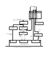
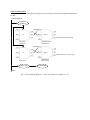
The hardware architecture of the present wire scanner system is shown in Fig.2. In this system,
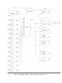
the beam gate signal, used for triggering ADC, is generated independently. The software architecture the
system is shown in Fig.3. An independent software thread is executed in the IOC to acquire data from
CAMAC hardware and store in a runtime ring buffer (event queue). The header of the buffer, comprising
of header length, size of the buffer and latest data position, is updated by the thread after storing a new
data into the buffer. A special EPICS record is used to read the buffer after completion of a scan. The
buffer is accessed by IOC and the data storing thread using a semaphore. Since the system does not use
timing system events, hence three additional ADC channels are used to identify the beam mode from
acquired data. The buffer length is 2048 data and each data, an array of 16bit integers, is comprised of
following elements.
6789"#"678:"#"67;9"#"67;:"#"67<9"#"67<:"#"67=9"#"67=:"#">78"#">7;"#">7<"#"?78"#"?7;"#@@@@@@@@"#"?78;"
Where: S-1H & S-1L: Higher 16bit and Lower 16bit of Scaler channel – 1 data (32 bit)
Similar for Scaler channel 2 to 4.
B-1 to B-3: 12 bit BPM ADC channel -1 to 3 data
A-1 to A-12: 12 bit ADC channel 1 to 12 data, used for PMT signals and beam mode
identification.
The buffer header (32 elements) configuration is as follows.
!"#$%&'%(")*+%"*,"-./%)"#"!"#"%&0$"'&/&")*+%"*,"-./%)"#"!"#"-122%(")*+%"#!"#"3&/%)/"'&/&"*,'%4"#"!"#5555555#"!""
At present, header size in bytes = 32 * 2 = 64, data size in bytes = 23 * 2 = 46 & buffer size = 2048
In the present system, at first the wire is moved from home position to final position i.e. inside beam line,
either at low, medium or high speed, depending on the beam mode and then back to the home position at
a high speed. After completion of the scan, the buffer is read and stored in 16 subarray (each contains 128
data array) record. The user panel (SAD) utilizes the data stored in the subarrays for its computation.
ABC"6D6ECB"FCGHI6"HJIK"
I" M"
G" G"
L" H"
>"
I?B?I"
6CNH?:"
HOECNP?IC"
ABC"
I?B?I"
HOECNP?IC"
M?EC"
MCOCN?EJN"
M?EC"G13)%"
IS,/(S3"Y"'&/&"*,/%(2&0%"
ABC"*,/%((1U/"S,"?QI":?B"
QHMHE?:""
BL:EH7BCECN"
GL:6C"BJEJN"
IJOENJ::CN"
IS,/(S3"
)*W,&3"
GS)*/*S,"FAS3/&W%K"
"P%%'-&0V"
I
J
O
:
N"
6"
I"
:"
N"
I" Q" "
6" ?"
?" I"
Q"
I"
G13)%"2%%'-&0V"
6ECGGCN"BJEJN"
QNHACN"
GSX%("
"S1/U1/"
GS/%,/*S7
T%/%("
I?B?I"6D6ECB"
GBE"
"S1/U1/"
GL:6C"BJEJN6"
"
!
"
>C?B"6I?OOCN"6D6ECB"
Fig. 2: Hardware architecture of the present system (CAMAC based)
IS,/(S3"
)*W,&3"
9HM9"AJ:E?MC"
GJRCN"6LGG:D"
9*W$"
ZS3/&W%"
GBE"
L6CN"HOECNP?IC"F6?QK"
A4RS(V)7_5_"
CGHI6"HJI"
•
•
•
I?B?I"Q?["E9NC?Q"
HE" IJOENJ:" E9C" GNJIC66" ?OQ"
?I[LHNC" Q?E?" PNJB" ?::"
6HMOO?:"6JLNIC6"
HE" NC?Q6" E9C" R9J:C" CACOE"
[LCLC" ?E" ?" EHBC" ?OQ" 6EJNC"
E9C" Q?E?" ?6" ?" 6GCIH?:" R?AC"
PJNB"NCIJNQ"
HE" 6COQ6" E9C" Q?E?" EJ" L6CN"
HOECNP?IC"L6HOM"I?"GNJEJIJ:"
•
•
•
HE" NLO6" ?6" ?O" HOQCGCOQCOE"
?GG:HI?EHJO"
HE" INC?EC6" CACOE" [LCLC"
BCBJND"L6HOM"L6CN"6GCIHPHCQ"
IJOPHMLN?EHJO"
HE"RNHEC6"6I?:CN\">GB"?OQ"R6"
?QI" Q?E?\" JO" :?B" HOECNNLGE"
JP" ?QI\" ?6" JOC" CACOE" HOEJ"
E9C"CACOE"[LCLC"
CACOE"[LCLC"FM:J>?:"BCBJNDK"
CACOE"7"!"
CACOE"]"8"
"
CACOE"7"4"
,"^"6I?:CN"
T""^">GB"
"
U"^"R6"
@55"
CACOE"7"O"
"
Fig. 3: Software Architecture of the present system (CAMAC based)
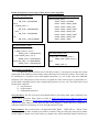
Developed system:
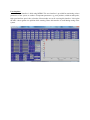
The hardware architecture of the developed system is shown in Fig.4. The configuration of this
system differs from the existing system in the following respects.
i)
ii)
iii)
iv)
v)
Motorola MVME5500 processor board is used.
It uses VME based CSADC, Scaler and DAC hardware.
It utilizes a VME based event receiver module (EVR-230RF) to synchronise the data
acquisition process with LINAC timing system.
A LAN/GPIB converter is used to communicate with Pulse motor controller (PMC) and
Digital Multimeter (DMM) for control and data acquisition.
An EPICS Base-3.14.12.1 based IOC, running on Vx-works 6.8, is used for control and
data acquisition.
The development process of this system may be divided into following phases.
i)
ii)
iii)
iv)
v)
vi)
vii)
viii)
ix)
x)
Building EPICS Base-3.14.12.1 with compact subarray support for Vx-works 6.8.
Development of EPICS device driver for CSADC, Scaler and DAC hardware.
Building EPICS device driver for Micro Research Finland make EVR-230RF event
receiver with EPICS Base-3.14.12.1 and Vx-works 6.8 CR/CSR support.
Configuration of the Firmware of EVR-230RF and tuning of the hardware with LINAC
timing system.
Programming EVR-230RF to generate gate pulse for CSADC trigger at desired event
with appropriate delay and width through EPICS records.
Tuning of the gate pulse (i.e. delay & width) generated by EVR-230RF with different
LINAC beam modes.
Development of pulse motor control algorithm for moving the wire scanner at variable
speed (i.e. low & high speed modes) while scanning the beam.
Integration of the system to acquire wire position and beam data on desired event and
store in an array for analysis.
Development of user panel, using MEDM, for control and monitoring the data acquisition
process.
Testing of the system.
Among the above steps, few major steps are described in details below.
Development of EPICS device driver:
In the wire scanner system, the secondary radiation caused by the beam after interaction
CSADC:
with wire scanner is collected by PMT placed at judicially selected locations along the LINAC beam line.
The output of the PMT is integrated using, M/s. Hoshin make, 14 bit, 8 channel charge integral type
VME6U ADC board (V005). This hardware is compatible to 24/16 bit addressing with 0x3d/0x2d address
modifying code. The detail specification is given below.
i)
ii)
Charge input: 0 to 1000 pc
Input impedance: 50 (negative signal)
iii) Gate width: 30 nsec to 1 usec
iv) Reset time: 400 nsec
v)
Conversion time: 15 usec
vi) Conversion type: Successive approximation
vii) Remaining pedestal: 1190 (approx)
viii) Resolution: 14 bit
ix) Linearity: ±0.03%
The address map of the board is as follows.
Read access (16 bit word type)
Channel-0: Base Address (2 byte)
Channel-1: Base Address + 0x02 (2 Byte)
…….
Channel-7: Base Address + 0x1e (2 Byte)
The MSB (15th bit) of each channel register is the LAM bit to signal the end of conversion.
Write access (16 bit word type)
Reset: The LSB (0th bit) of channel 0 register is to be set to ‘1’.
Scaler: The position of the wire scanner is read by counting the pulse output from Pulse motor controller.
A 32 bit, Hoshin make, 150 MHz scaler/counter hardware (V004) is used for this purpose. This hardware
is compatible to 24/16 bit addressing with 0x3d/0x2d address modifying code. The register details of the
hardware are as follows.
Read access (16 bit word type)
Channel-0: Base Address (4 byte)
Channel-1: Base Address + 0x04 (4 Byte)
…….
Channel-7: Base Address + 0x1c (4 Byte)
Write access (16 bit word type)
Start: Resetting lower byte at Base Adress + 0x02 (2 byte).
Stop: Resetting lower byte at Base Adress +0x04 (2 byte).
Reset: Resetting lower byte at Base Adress +0x0 8 (2 byte).
DAC: A high voltage power supply is used to control the bias voltage of PMT. The output of this power
supply is controlled by providing 0-10V DC at the analog input from the DAC board. A Prefort make 12
bit DAC hardware (PVME 323) is used for this purpose. This hardware is compatible to 24/16 bit
addressing with 0x3d/0x2d address modifying code. The technical specification of the hardware is as
follows.
i) Output range: 0 ~ 2.5V, 0 ~ 5.0V, 0 ~ 10.0V, ±2.5V, ±5.0V & ±10.0V
ii) Resolution: 12 bit
iii) Conversion time: 10 usec
iv) Stability: ±50ppm/C
v) Linearity: ±0.013%
The register details of the hardware are as follows.
ABC"*,/%((1U/"
M?EC"
U13)%"
ABC"6D6ECB"FCGHI6"HJIK"
I"
6"
I"
G" :"
L" N"
I" Q"
6" ?"
?" I"
Q"
I"
"
C
A
N"
IS,/(S3":?O"
CZ%,/)"
:?O`MGH>"
M&/%X&."
QHMHE?:""
BL:EH7BCECN"
CACOE"
MCOCN?EJN"
6ECGGCN"BJEJN"
IJOENJ::CN"
IS,/(S3"
)*W,&3"
6ECGGCN"BJEJN"
QNHACN"
GS)*/*S,"FAS3/&W%K"
"P%%'-&0V"
GSX%("
"S1/U1/"
B?M5"
6I?:C"
IS,/(S3"
)*W,&3"
G13)%"2%%'-&0V"
GBE"
"S1/U1/"
6ECGGCN"BJEJN6"
"
!
"
>C?B"6I?OOCN"6D6ECB"
Fig. 4: Hardware architecture of the developed system
9HM9"AJ:E?MC"
GJRCN"6LGG:D"
9*W$"
ZS3/&W%"
GBE"
Write access (16 bit word type)
Channel-0: Base Address + 0x30 (2 byte)
Channel-1: Base Address + 0x32 (2 byte)
…………
Channel-7: Base Address + 0x3e (2 byte)
EPICS Device driver: The EPICS device drivers, compatible to Vx-works 6.8, are developed for the
above hardware using EPICS Base-3.14.12.1 with CSA support. There are longin, bi, bo and waveform
record support for CSADC & Scaler hardware. The DAC hardware has only analog out (ao) record
support. 24 bit addressing mode is chosen for the hardware in device driver. The following functions are
provided for configuring the hardware during EPICS IOC initialization.
CSADC: devHoshinV005Config(int x, long y)
Scaler: devHoshinV004Config(int x, long y)
DAC: devPvme323Config(int x, long y)
Where x = Number of cards used
y = Starting Physical address (24 bit) of the hardware
A maximum number of 10 similar hardware, with physical addresses separated by a buffer of appropriate
size, can be configured by using the above functions.
Development of Micro Research Finland EVR-230RF support:
The Micro Research Finland (MRF) EVR-230RF event receiver board is used to integrate the
system with LINAC timing system. The detail specification and the user manual of the hardware are
available at the following link.
http://www.mrf.fi/index.php/vme-products/75-vme-event-receiver-rf-vme-evr-230rf
This hardware provides CR/CSR suport as specified in VME64x specification. The device support
module, available under “Hardware support: by Manufacturer->Micro Research Finland” in EPICS home
page, is used for VME based EVR-230RF module. EPICS devLib2 and MSI tool are the prerequisite for
building this module. Since the present version of EPICS does not support CR/CSR address space in
operating system independent manner. The devlib2 is the support modules, which enables operating
system independent bus address translation in EPICS. The source of this module and support tools are
listed below.
i)
ii)
iii)
iv)
MRF EVR-230RF support module (mrfioc2-2.0.0.tar.gz):
http://sourceforge.net/projects/epics/files/mrfioc2/
MRF EVR-230RF support module (mrfioc2-2.0.0.tar.gz) bug fix:
http://epics.hg.sourceforge.net/hgweb/epics/mrfioc2/
EPICS devLib2 module (devlib2-2.2.tar.gz):
http://sourceforge.net/projects/epics/files/devlib2/
EPICS MSI tool (msi1-5.tar.gz):
http://www.aps.anl.gov/epics/extensions/msi/index.php
The devlib2-2.2 module and msi1-5 extension are built by incorporating the EPICS base location
(EPICS_BASE) in the respective RELEASE files. The path of msi executable should be included in the
PATH environmental variable before building the mrfioc2-2.0.0 module. After expanding the mrf1oc22.0.0 module, the RELEASE file is modified to incorporate the following line.
DEVLIB2=<path>/devlib2-2.2
EPICS_BASE=<path>/base-3.14.x
The module is built by issuing make command from top folder. After building, the content of the Top
folder is shown below.
drwxr-xr-x 4
-rw-r--r-- 1
drwxr-xr-x 5
drwxr-xr-x 2
drwxr-xr-x 2
drwxr-xr-x 3
-rw-r--r-- 1
drwxr-xr-x 6
drwxr-xr-x 4
drwxr-xr-x 5
-rw-r--r-- 1
drwxr-xr-x 5
drwxr-xr-x 4
drwxr-xr-x 4
-rw-r--r-- 1
-rw-r--r-- 1
-rw-r--r-- 1
drwxr-xr-x 3
drwxr-xr-x 5
drwxr-xr-x 4
-rw-r--r-- 1
-rw-r--r-- 1
r_ani games 4096 May 23 17:04
r_ani
games 110
Feb 15 14:26
r_ani
games 4096 May 23 17:20
r_ani
games 4096
May 23 17:06
r_ani
games 4096 May 23 17:06
r_ani games 4096 Feb 15 14:26
r_ani
games 47626 Feb 15 14:26
r_ani
games 4096
Feb 15 14:26
r_ani
games 4096
Feb 15 14:26
r_ani
games 4096
Feb 15 14:26
r_ani
games 984
Feb 15 14:26
r_ani games 4096
May 23 17:04
r_ani
games 4096
Mar 12 19:37
r_ani
games 4096
May 23 17:03
r_ani
games 3543
Feb 15 14:26
r_ani
games 968
Feb 15 14:26
r_ani
games 40297 Feb 15 14:26
r_ani
games 4096
Feb 15 14:26
r_ani
games 4096 Feb 15 14:26
r_ani games 4096
Feb 15 14:26
r_ani
games 1335
Feb 15 14:26
r_ani
games 317
Feb 15 14:26
bin
Changelog
configure
db
dbd
documentation
Doxyfile
evgMrmApp
evrApp
evrMrmApp
evrtg.txt
include
iocBoot
lib
LICENSE
Makefile
make-log-mrfioc2-2-0-0.txt
mrfCommon
mrmShared
mrmtestApp
README
TODO.evr
Tuning of EVR230RF:
Before using EVR-230RF, the reference clock of the module is to be synchronise with the
incoming events from event generator. For flexibility, a programmable reference clock is provided to
allow the use of the module in various applications with varying frequency requirements. The clock
reference for the event receiver is generated on-board using a fractional synthesizer. A Micrel SY87739L
Protocol Transparent Franctional-N synthesizer with a reference clock of 24 MHz is used for this purpose.
The detail procedure for calculating the configuration bit pattern of the franctional synthesizer is available
in the respective hardware datasheet (http://www.micrel.com/PDF/HBW/sy87739l.pdf).
In the present case, LINAC timing system uses an event clock rate of 114.25 MHz. This clock
frequency is obtained from the synthesizer’s reference clock, 24 MHz, by using the following formula.
Event rate (MHz) = [ (M/N)*[P - (Q(p-1)/(Qp + Q(p-1))] * Fref ]/PostDivSel
Where,
Fref = 24.0 MHz
PostDivSel = 6
M = 14, N = 14, therefore M/N = 1
P = Mod[(Event rate X postDivSel)/Fref] = 29
Q(p-1) = 14
Qp = 32 – Q(p-1) = 18, as Qp + Q(p-1) = 32
The corresponding configuration bit pattern (word) is
0000-Qp(5)-Q(p-1)(5)-P(4)-000-PostDivSel(5)-N(3)-M(3)
as per datasheet. Hence by substituting the values of PostDivSel, M, N, P, Qp & Q(p-1) from the datasheet,
i.e. Qp = 10010, Q(p-1) = 01110, P = 1100, PostDivSel = 00110, M = 101, N = 101, the final configuration
word for 114.25 MHz is
093B01AD (0000-10010-01110-1100-000-00110-101-101).
This configuration word is stored into EVR-230RF non-volatile memory using the 10baseT network
interface of the module in the following procedure.
i)
Telnet to the IP assigned to EVR-230RF and issue following commands from telnet
prompt
ii)
Use command ‘b’ to see/change the synthesizer configuration word, boot parameters, IP
address, DHCP setting etc. of the module
iii) Change the configuration word
iv) Use command ‘s’ to save the values in memory
v)
Use command ‘r’ to reset the board to effect the changed parameter values
vi) Connect the optical fiber from event generator into EVR-230RF front panel
vii) Telnet to EVR-230RF and issue following commands from telnet prompt
viii) Use command ’t’ to tune delay line
ix) Use command ‘s’ to save the new delay line value into memory
Fig 4: Telnet prompt after issuing tuning command
Programming of EVR230RF:
The detail description of the EPICS device support module for EVR-230RF is available at the
following link.
https://pubweb.bnl.gov/~mdavidsaver/files/evr-usage-r4.pdf
EVR-230RF module is configured while IOC initialization using the following function
mrmEvrSetupVME("EVR1", 6, 0x08000000, 5, 0x20)
Where EVR1 = object name used to link the module with EPICS records
6 = VME slot number
0x8000000 = System address for mapping
5 = interrupt level
0x20 = interrupt vector
The EPICS records, used to configure the EVR-230RF module, are described in details below. In these
records, the EVR-230F module is identified by the object name (e.g. @OBJ = EVR1) provided for
parameter @OBJ in the records’ INP/OUT property. Every record is associated with a specific device
type and PROP field value depending upon the property to be controlled or monitored. There are four sets
of records for configuration of EVR-230RF module, pulse-generator, front panel output and EPICS event
generation.
Records for configuring of EVR-230RF module:
The object name is “EVR1” and the device type is either of “Obj Prop bool” (bo & bi records), “Obj Prop
double” (ao & ai records) and “Obj Prop unit32” (longout & longin records).
# To enable EVR-230
field(DESC, "Timestamp tick rate")
field(VAL , "1.0")
record(bo, "EVR1:Ena-Sel") {
field(EGU , "MHz")
field(DTYP, "Obj Prop bool")
field(LINR, "LINEAR")
field(OUT , "@OBJ=EVR1, PROP=Enable")
field(ESLO, "1e-6")
field(DESC, "Master enable for EVR device")
field(HOPR, "150")
field(MASK, "1")
field(LOPR, "0")
field(VAL, "1")
field(DRVH, "150")
field(ZNAM, "Disabled")
field(DRVL, "0")
field(ONAM, "Enabled")
field(PREC, "3")
field(PINI, "YES")
}
}
# Set Clock frequency to 114.25 MHz
record(ao,"EVR1:Clk-SP")
{
field(DTYP, "Obj Prop double")
field(OUT, "@OBJ=EVR1, PROP=Clock")
field(VAL, "114.25")
field(LINR, "LINEAR")
field(ESLO, "1e-6")
}
# Set timestamp source – 0 i.e. event clock
record(longout, "EVR1:TimeStamp-Src")
{
field(DTYP, "Obj Prop uint32")
field(OUT , "@OBJ=EVR1,
PROP=Timestamp Source")
field(VAL, "0")
}
# Set timestamp clock prescaler
record(ao, "EVR1:Time:Clock-SP") {
field(DTYP, "Obj Prop double")
field(OUT , "@OBJ=EVR1,
PROP=Timestamp Clock")
# Readback PLL status
record(bi,"EVR1:PLL-Sts")
{
field(DTYP, "Obj Prop bool")
field(INP,"@OBJ=EVR1, PROP=PLL Lock Status")
field(SCAN, ".1 second")
field(ZNAM, "Fail")
# Readback clock frequency
record(ai,"EVR1:Clk")
{
field(DTYP, "Obj Prop double")
field(INP, "@OBJ=EVR1, PROP=Clock")
field(EGU , "MHz")
field(LINR, "LINEAR")
field(ESLO, "1e-6")
field(PREC, "3")
}
# Set on Heartbit failure (detection)
record(longin, "EVR1:HB:Timeout") {
field(DTYP, "Obj Prop uint32")
field(INP , "@OBJ=EVR1, PROP=HB
Timeout Count")
field(SCAN, "I/O Intr")
field(DESC, "# of heartbeat timeout")
}
field(ONAM, "OK")
}
# Readback Link status
record(bi, "EVR1:Link-Sts")
{
field(DTYP,"Obj Prop bool")
field(INP, "@OBJ=EVR1, PROP=Link Status")
field(SCAN, ".1 second")
field(ZNAM, "Fail")
field(ONAM, "OK")
}
Record for mapping front panel output with pulse-generator:
The object name is “EVR1:FrontOut0” for Front panel output – 0 and device type is “Obj Prop unit32”
(longout record).
record(longout, "EVR1:FP0:Src-SP") {
field( DTYP, "Obj Prop uint32")
field( DESC, "OUT0 (TTL)")
field( OUT , "@OBJ=EVR1:FrontOut0, PROP=Map")
field( FLNK, "EVR1:FP0:Src-RB")
field( PINI, "YES")
field( VAL , "0") // 0 for pulse-generator 0
}
Records for configuring pulse-generator:
The object name is “EVR1:Pul0” for Pulser 0 and device type is either of “Obj Prop bool” (bo & bi
records), “Obj Prop double” (ao & ai records) and “Obj Prop unit32” (longout & longin records).
# Enable pulse generator 0
record(bo, "EVR1:DlyGen0:Ena-Sel") {
field(DTYP, "Obj Prop bool")
field(OUT , "@OBJ=EVR1:Pul0, PROP=Enable")
field(PINI, "YES")
field(VAL , "1")
field(MASK, "1")
field(ZNAM, "Disabled")
field(ONAM, "Enabled")
}
# Set polarity Active Low (val = 1)
record(bo, "EVR1:DlyGen0:Polarity-Sel") {
field(DTYP, "Obj Prop bool")
field(OUT , "@OBJ=EVR1:Pul0, PROP=Polarity")
field(PINI, "YES")
field(VAL , "1")
field(MASK, "1")
field(ZNAM, "Active High")
field(ONAM, "Active Low")
}
# Set Delay (val = 40usec)
record(ao, "EVR1:DlyGen0:Delay-SP") {
field(DTYP, "Obj Prop double")
field(OUT , "@OBJ=EVR1:Pul0, PROP=Delay")
field(PINI, "YES")
field(DESC, "Pulse Generator 0")
field(VAL , "40")
field(EGU , "us")
field(LINR, "LINEAR")
field(ESLO, "1e6")
field(PREC, "3")
field(FLNK, "EVR1:DlyGen0:Delay-RB")
}
# Readback delay setting in usec
record(ai, "EVR1:DlyGen0:Delay-RB") {
field(DTYP, "Obj Prop double")
field(INP , "@OBJ=EVR1:Pul0, PROP=Delay")
field(VAL , "0")
field(EGU , "us")
field(LINR, "LINEAR")
field(ESLO, "1e6")
field(PREC, "3")
field(FLNK, "EVR1:DlyGen0:Delay:Raw-RB")
}
# Readback delay setting in count (raw)
record(longin, "EVR1:DlyGen0:Delay:Raw-RB") {
field(DTYP, "Obj Prop uint32")
field(INP , "@OBJ=EVR1:Pul0, PROP=Delay")
field(EGU , "cnts")
field(HOPR, "0xffffff")
field(LOPR, "0")
field(HIGH, "0xffffff")
field( HSV, "MAJOR")
}
# Set pulse width (100 nsec)
record(ao, "EVR1:DlyGen0:Width-SP") {
field(DTYP, "Obj Prop double")
field(OUT , "@OBJ=EVR1:Pul0, PROP=Width")
field(PINI, "YES")
field(DESC, "Pulser pulse width")
field(VAL , "100")
field(EGU , "ns")
field(LINR, "LINEAR")
field(ESLO, "1e9")
field(PREC, "3")
field(FLNK, "EVR1:DlyGen0:Width-RB")
}
# Readback pulse width in nsec
record(ai, "EVR1:DlyGen0:Width-RB") {
field(DTYP, "Obj Prop double")
field(INP , "@OBJ=EVR1:Pul0, PROP=Width")
field(VAL , "0")
field(EGU , "ns")
field(LINR, "LINEAR")
field(ESLO, "1e9")
field(PREC, "3")
field(FLNK, "EVR1:DlyGen0:Width:Raw-RB")
}
# Readback pulse width in count (raw)
record(longin, "EVR1:DlyGen0:Width:Raw-RB") {
field(DTYP, "Obj Prop uint32")
field(INP , "@OBJ=EVR1:Pul0, PROP=Width")
field(PINI, "YES")
field(HOPR, "0xffff")
field(LOPR, "0")
field(HIGH, "0xffff")
field( HSV, "MAJOR")
}
# Set Prescaler value (val = 1)
record(longout, "EVR1:DlyGen0:Prescaler-SP") {
field(DTYP, "Obj Prop uint32")
field(OUT , "@OBJ=EVR1:Pul0, PROP=Prescaler")
field(DESC, "Pulser prescaler")
field(PINI, "YES")
field(HOPR, "0xff")
field(LOPR, "1")
field(DRVH, "0xff")
field(DRVL, "1")
field(VAL , "1")
field(FLNK, "EVR1:DlyGen0:Prescaler-RB")
field(DISP, "0")
field(DISA, "0")
}
# Readback Prescaler setting
record(longin, "EVR1:DlyGen0:Prescaler-RB") {
field(DTYP, "Obj Prop uint32")
field(INP , "@OBJ=EVR1:Pul0, PROP=Prescaler")
field(HOPR, "0xff")
field(LOPR, "1")
field(HIGH, "0xff")
field( HSV, "MAJOR")
field(FLNK, "EVR1:DlyGen0:Res-I")
}
Record for mapping timing event to pulse-generator:
The following record is used to map an event (val = 51) to a pulse-generator (@OBJ=EVR1:Pul0,
Func=$(F=Trig)). The corresponding device type is “EVR Pulser Mapping”.
# Mapping pulser-0 to a event code e.g. 51
record(longout, "LIiEV:KEKB:Pul0:Evt") {
field( DTYP, "EVR Pulser Mapping" )
field( OUT , "@OBJ=EVR1:Pul0, Func=$(F=Trig)")
field( PINI, "YES")
field( DESC, "Mapping for Pulser 0")
field( VAL , "51")
field( LOPR, "0")
field( HOPR, "255")
field( DRVL, "0")
field( DRVH, "255")
}
Record for mapping timing event to EPICS event:
The following record is used to generate an EPICS event (val=30) from the incoming event (code = 31) to
EVR-230RF. Here the device type is “EVR Event”.
record(longout, "EVR1:event:31") {
field(DTYP, "EVR Event")
field(SCAN, "I/O Intr")
field(OUT , "@OBJ=EVR1,Code=31")
field(VAL , "30")
field(TSE , "-2")
}
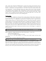
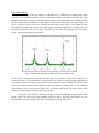
Pulse motor control:
The movement of the wire scanner is controlled from a GPIB based 4 channel pulse motor
controller. A LAN/GPIB converter is used to communicate with the pulse motor controller. The pulse
feedback output of the controller is used for monitoring the wire position through scaler. During scanning,
the wire scanner interacts with beam at three distinct regions of the total span of movement. Hence it is
wise to control the speed of the wire such that the wire should move slowly in the region of beam
interaction to get more valid data and fast in other region to minimize scanning time. To achieve this, the
total span of movement of the wire scanner is divided into seven zones. The fig below shows the various
regions with associated speed of movement.
Fig. 5: Schematic showing peak position and various scanning zones
The direction of movement is also divided into three types e.g. forward (2), backward (3) and from any
position to home (1). The last direction is useful when the wire scanner is kept in between position due to
some manual operation. In the present system, the pulse motors are driven in ABSOLUTE SCAN mode
to prevent overdrive beyond the final position of the wire scanner i.e. SPAN. There are two hardware
limit switches at the two end of wire scanner drive to stop the pulse motor. The status of these limit
switches are also monitored from the supervisory interface.
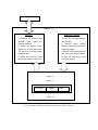
To move the wire scanner in multi-speed mode, an auto scan algorithm is implemented in the
present system. The flow chart of the algorithm is shown in Fig 6. The limit switch statuses are also
included in the auto scan method to stop wire movement on activating a limit switch.
6E?NE"
F?LEJa6I?Ob8K"
?"
6CE"NCBJEC"BJQC"
FNCBcIBQb8K"
R?HE"PJN"8!!"T)%0"
FQC:?DK"
6E?NE"BJAHOM"
F6E?NEK"
6CE":JR"6GCCQ"
F:6GQaREbd\";!!UU)K"
NC?Q"GJ6HEHJO"
FGJ6OK"
6CE"BCQ"6GCCQ"
F:6GQaREb;8\"8!!!UU)K"
6CE"9HM9"6GCCQ"
F:6GQaREb=8\"<!!!UU)K"
GJ6OaI?:I"
"""""""
I9CIh"6E?EL6"
F>L6DaP:?M"b"8K"
DC6"
OJ"
6CE"QHNCIEHJOe"
FQHNaP:?Mb8`;`<K"
GJ6O"b"QH6E?OIC"F6E?NE5A?:K"
OJ"
DC6"
6CE"fJOCe"
FfJOCaP:?Mb!`8`;`<`=`_`g`dK"
6CE"6GCCQe"
F6GCCQb9H`:JRK"
DC6"
QHNaP:?M"i"<"F>?IhR?NQK"
OJ"
6EJG"
6CE"QH6E?OICe"
F6E?NE5A?:K"
?"
Fig. 6: Flow chart of Pulse motor control algorithm (*Steps are described in detail in next section)
Details description of various steps of Pulse motor control algorithm:
6CE"QHNCIEHJO"FQHNaP:?MKc"
HP"GJ6HEHJO"b"!"FH5C5"9JBCK"
"
QHNaP:?M"b";"FPJNR?NQK"
C:6C"HP"
""""""HP"fJOCaP:?M"b"d""
"
QHNaP:?M"b"<"F>?IhR?NQK"
""""""C:6C"
"
QHNaP:?M"b";"FPJNR?NQK"
C:6C"
"
QHNaP:?M"b"8"FMJEJ"9JBCK"
6CE"6GCCQ"F6GCCQaP:?MKc"
HP"QHNaP:?M"b";"FPJNR?NQK"
"""""HP"fJOCaP:?M"b"!\"8\<\_\d"
"
6GCCQaP:?M"b";"F9HM9"6GCCQK"
"""""C:6C"HP"fJOCaP:?M"b";\"=\"g"
"
6GCCQaP:?M"b"!"F:JR"6GCCQK"
"C:6C"HP"QHNaP:?M"b"<\"8"F>?IhR?NQK"
"
6GCCQaP:?M"b";"F9HM9"6GCCQK"
6CE"QH6E?OIC"F6E?NEa6C:"Y"?LEJaI?:IKc"
6RHEI9"FfJOCaP:?MK"
"
I?6C"!c"6E?NE"b"!"F9JBCK"
I?6C"8c"6E?NE"b"GC?h8a6E?NE"
I?6C";c"6E?NE"b"GC?h8aCOQ"
I?6C"<c"6E?NE"b"GC?h;a6E?NE"
I?6C"=c"6E?NE"b"GC?h;aCOQ"
I?6C"_c"6E?NE"b"GC?h<a6E?NE"
I?6C"gc"6E?NE"b"GC?h<aCOQ"
I?6C"dc"6E?NE"b"6G?O"
6CE"fJOC"FfJOCaP:?MKc"
HP"QHNaP:?M"b";"Y"fJOCaP:?M"j"d"
"
fJOCaP:?M"b"fJOCaP:?M"k"8"
C:6C"
"
fJOCaP:?M"b"!"
"""""""
Wire-scanner record (WS):
An application specific EPICS record, WS (Wire Scanner), is developed to meet the data format
requirement of the SAD based wire-scanner control and analysis user interface software. This record may
be considered as a waveform record with multiple input-links, e.g. calc record, with some additional
parameters. The main purpose of this record is to append the values retrieved from its input-links in a
circular buffer depending upon its other configuration parameter on every scan. The fields in this record
fall into these categories:
a) scan parameters
b) read parameters
c) configuration parameters
Scan parameter: The WS record has the standard fields for specifying under what circumstances the
record will be processed. These fields are listed in EPICS Record Reference Manual (Scan Fields,
Chapter 2, 2). In addition, EPICS Record Reference Manual (Scanning Specification, Chapter 1, 1),
explains how these fields are used. Since the WS record supports no direct interfaces to hardware, it
cannot be scanned on I/O interrupt, so its SCAN field cannot be I/O Intr.
Read parameter: The record consists of 52 input-links INPA, INPB,. . . INPZ, INPAA….INPAZ. These
fields can be database links, channel access links or constants. If they are links, they must specify another
record's field or a channel access link. If they are constants, they will be initialized with the value they are
configured with and can be changed via dbPuts. They cannot be hardware addresses. See EPICS Record
Reference Manual (Address Specification, Chapter 1, 2), for information on how to specify database links.
Field
Summary
INPA
Input Link A
INLINK Yes 0
No
No
N/A
INPB
Input Link B
INLINK Yes 0
No
No
N/A
INPC
Input Link C
INLINK Yes 0
No
No
N/A
INPD
Input Link D
INLINK Yes 0
No
No
N/A
INPE
Input Link E
INLINK Yes 0
No
No
N/A
INPF
Input Link F
INLINK Yes 0
No
No
N/A
INPG
Input Link G
INLINK Yes 0
No
No
N/A
INPH
Input Link H
INLINK Yes 0
No
No
N/A
INPI
Input Link I
INLINK Yes 0
No
No
N/A
INPJ
Input Link J
INLINK Yes 0
No
No
N/A
...
...
...
...
...
...
INPZ
Input Link Z
INLINK Yes 0
No
No
N/A
INPAA Input Link AA INLINK Yes 0
No
No
N/A
...
...
...
...
No
No
N/A
...
Type
...
DCT Initial Access Modify Rec Proc Monitor
...
...
...
...
INPAZ Input Link AZ INLINK Yes 0
Configuration parameter: The record has following configuration parameters for calibration of scaler
data using BPM data, delay to process the record and setting data format. The record always considers the
first NSCLR number of input-links from (INPA) as scaler channel and stores each scaler data as two 16
bit integer (MSB then LSB). The next 3 x NBPM input-links are considered as BPM ADC data. For each
BPM, these data are stored as three 16 bit interger. Then the next NWS input-links are considered as wire
scanner ADC data and each ADC data is stored as one 16 bit integer. The event number (NEVNT) is then
appended to the above data as one 16 bit integer.
Field
Summary
NSCLR Number of scaler channel
Type
DCT Initial Access Modify
Rec Proc
Monitor
SHORT
Yes 0
No
No
N/A
Number of BPM data to be stored. Every
NBPM BPM data is a set of three or four elements SHORT
depending on CLBF flag is 1 or 0.
Yes 0
No
No
N/A
NWS
SHORT
Yes 0
No
No
N/A
SHORT
Yes 0
No
No
N/A
Calibration flag, if 1, then BPM ADC data
will be used to calibrate the wire scanner
scaler data
If 0, then raw scaler data will be inserted SHORT
into the array
Note: calibration of scaler data is not yet
implemented
Yes 0
No
No
N/A
Number of ADC data to be stored
NEVNT Event number to be append
CLBF
DLY
Delay value in millisecond. The record
will be processed after this value during
every scan. This is to ensure the
completion of ADC data conversion.
DOUBLE Yes 0
Yes
Yes
Yes
Yes
Number of data set consisting of scaler,
BPM, wire scanner and event number, to
NELM be stored. Hence the size of the buffer will ULONG Yes 0
be
2*NSCLR + 3*NBPM + NWS + 1
No
No
N/A
FTVL
No
No
N/A
Rearm flag. If 1, then the buffer will be reRARM initialised and NORD will be set to 0 on
SHORT
next scan process.
Data type, always to be “SHORT”
MENU
Yes 0
Yes 0
N/A
An example configuration of the above record is shown below.
record(ws, "$(user)BTiWSBPM:L61:DATAW")
{
field(CNF, "/users/r_ani/epics/epics312vw67/modules/WS/calibdata/btarwb-104.cal")
# scaler - 4
# Beam gate pulse signal
field(INPA, "$(user)BTiWSBPM:L61:SCALER:ch0.VAL PP")
# Pulse motor controller signal
field(INPB, "$(user)BTiWSBPM:L61:SCALER:ch1.VAL PP")
field(INPC, "$(user)BTiWSBPM:L61:SCALER:ch2.VAL PP")
field(INPD, "$(user)BTiWSBPM:L61:SCALER:ch3.VAL PP")
# BPM - 1 (3 ch)
field(INPE, "$(user):L61:SP_48_4_1:X:PFE.VAL PP")
field(INPF, "$(user):L61:SP_48_4_1:Y:PFE.VAL PP ")
field(INPG, "$(user):L61:SP_48_4_1:I:PFE.VAL PP ")
# WS - 4
field(INPH, "$(user)BTiWSBPM:L61:ADC:ch0.VAL PP")
field(INPI, "$(user)BTiWSBPM:L61:ADC:ch1.VAL PP")
field(INPJ, "$(user)BTiWSBPM:L61:ADC:ch2.VAL PP")
field(INPK, "$(user)BTiWSBPM:L61:ADC:ch3.VAL PP")
field(INPL, "$(user)BTiWSBPM:L61:ADC:ch4.VAL PP")
field(INPM, "$(user)BTiWSBPM:L61:ADC:ch5.VAL PP")
# PMT C & D
field(INPN, "$(user)BTiWSBPM:L61:ADC:ch6.VAL PP ")
field(INPO, "$(user)BTiWSBPM:L61:ADC:ch7.VAL PP")
field(INPP, "0")
field(INPQ, "0")
field(INPR, "0")
field(INPS, "0")
field(NSCLR, "4")
field(NBPM, "1")
field(NWS, "12")
field(NEVNT, "0")
field(NELM,"2048")
field(FTVL, "SHORT")
field(SCAN, "Passive")
field(EVNT, "0")
field(PINI, "NO")
# msec delay before reading
field(DLY, "0.002")
# BPM calibration disabled
field(CLBF, "1")
field(FLNK, "$(user)BTiWSBPM:L61:DATAWF")
}
The header configuration of the new WS record is as shown below, where index is the element position of
in the header array.
Index
Description
0
Total number of header elements or header
size = 32
2
Size of the header in bytes = 64
4
Size of each event data in bytes = 48
6
Size of buffer = 2048 (number of event)
8
Pointer to latest data
10
Number of scaler
12
Number of BPM
14
Number of WS ADC
Software architecture:
This section describes the processing various records on events and the linkage among various
records.
CZ%,/")%l1%,0%"
CACOE7,"
OGG"OB6"
&S"
3S,WS1/"
mJ>nbCAN8cG13!\"GNJGbQ%3&."
M&/%7Q%3&."
6I?OcCZ%,/"
Q3.M%,!cQ%3&.76G"
6I?Oc"G&))*Z%"
OGG"OB6"
&S"
3S,WS1/"
mJ>nbCAN8cG13!\"P1,0boFPbE(*WK"
M&/%7G13)%"
6I?Oc"CZ%,/"
CACOE7F,k8K"
hCh>cG13!cCZ/"
6I?Oc"G&))*Z%"
:H*CAchCh>cGP"
/*T%"
Fig. 7: Record linkage diagram – 1 (PF event is taken as example, n = 51)
Fig. 8: Record linkage diagram – 2 (PF event is taken as example, n = 51)
User interface:
The user interface is built using MEDM. This user interface is provided for monitoring various
parameters of the system. A number of important parameters e.g. peak positions, widths around peaks,
high speed and low speed value, selection of beam modes etc can be set using this interface. It also plots
the ADC values against wire position while scanning. Hence this interface is useful during testing of the
system.
Test result:
Location of Various source codes:
Server: abco4.kek.jp
User: r_ani (aicg123)
Wire scanner IOC: /users/r_ani/epics/epics3121vw68/modules/ws_mrfioc2
User interface: /users/r_ani/epics/epics3121vw68/modules/display/BTL61_WS_OPI.adl
List of IOC source files:
Directory: ws_mrfioc2/wsApp/src
devHoshinV004.c
devHoshinV005.c
devPvme323.c
devWsRecordBpm.c
devWsRecord.dbd
devXxHP4970AWS.c
devXxHP4970AWS.dbd
devXxHP4970AWS.gt
devXxHP4970AWS.list
devXxPM4CGpib.c
devXxPM4CGpib.dbd
devXxPM4CGpib.gt
devXxPM4CGpib.list
hoshinV004.dbd
hoshinV005.dbd
Makefile
pvme323.dbd
timeDelayRecord.c
timeDelayRecord.dbd
wsAppMain.cpp
wsRecordBpm.c
wsRecord.dbd
Directory: ws_mrfioc2/iocBoot/iocwsApp
cdCommands
Makefile
st.cmd
Directory: ws_mrfioc2/wsdb
BTL61wsdata_csa_bpm.db
BTL61wsdata_csa_5bpm.db
BTL61hv.db
BTL61wsmove_A_wire.db
BTL61wsmove_B_wire.db
BTL61wsmove_C_wire.db
BTL61wsmove_D_wire.db
BTL61wsmove_HP4970AWS.db
BTL61wsmove_newpmc.db
evr-kekb-config.db
evr-kekb-events.db
evr-kekb-events-enable.db
evr-kekb-pulsermap.db
hoshinV004.db
hoshinV005.db
List of important records: (Note: “R:” is added to distinguish from existing records. “R:” should be removed for final installation.)
1. Pulse motor control & monitoring
&'(%)*#$+,'#
!"#$%#
-(('..#
/0121+"#3+"4'#
5012#
!(+0#
64)7%.'#
!
"!
:1)'#-#*)1;'#.<.2',#
#$%&'()$*+,-$).-/!
(0'12!
"33433!
55!
.677'82!
)211'9:!7;69!
<!
#$%&'()$*+,-$.=->"!
(0'12!
<34<+!
55!
.677'82!
)211'9:!?'02"!;26@!;A7'1'A9!
B!
#$%&'()$*+,-$(CD&E"!
(0'12!
"F433!
55!
.677'82!
)211'9:!?'02"!?'G1H!60AI9G!;26@!
J!
#$%&'()$*+,-$.=-><!
(0'12!
JF4K+!
55!
.677'82!
)211'9:!?'02<!;26@!;A7'1'A9!
+!
#$%&'()$*+,-$(CD&E<!
(0'12!
"J433!
55!
.677'82!
)211'9:!?'02<!?'G1H!60AI9G!;26@!
F!
#$%&'()$*+,-$.=->B!
(0'12!
KK4+L!
55!
.677'82!
)211'9:!?'02B!;26@!;A7'1'A9!
K!
#$%&'()$*+,-$(CD&EB!
(0'12!
"<433!
55!
.677'82!
)211'9:!?'02B!?'G1H!60AI9G!;26@!
L!
#$%&'()$*+,-$*).D,(&!
(0'12!
K433!
MAI91!
.677'82!
)211'9:!NA?!7;22G!86NI2!
O!
#$%&'()$*+,-$E).D,(&!
(0'12!
J"433!
MAI91!
.677'82!
)211'9:!H':H!7;22G!86NI2!
"3!
#$%&'()$*+,-$P(*)!
#26G!
Q!
!
4"!72M!
P(!N'5'1!7?'1MH!026GR6M@!
""!
#$%&'()$*+,-$PP(*)!
#26G!
Q!
!
4"!72M!
PP(!N'5'1!7?'1MH!026GR6M@!
"<!
#$%&'()$*+,-$.S)/!
#26G!
Q!
MAI91!
4"!72M!
('02!;A7'1'A9!
"B!
#$%&'()$*+,-$)&-&T)!
#26G!
Q!
!
4"!72M!
D0'82!7161I7!U!)&S.V!#T/!V!%-P>!
"J!
#$%&'()$*+,-$-T&S,)P-/!
(0'12!
3433!
!
.677'82!
&A!71601!7M699'9:V!?0'12!"!
"+!
#$%&'()$*+,-$-%)S*T&=,)P-/!
(0'12!
3433!
MAI91!
.677'82!
&A!5A82!?'02!61!69W!;A7'1'A9!XG2Y6IN1!'7!HA52Z!
"F!
#$%&'()$*+,-$P-/P=*!
(0'12!
"433!
!
.677'82!
&A!M69M2N!7M699'9:!69G!5A82!1A!HA52!
!
!
!
!
!
!
!
!
:1)'#=#*)1;'#.<.2',#
"!
(0'12!
"33433!
55!
.677'82!
)211'9:!7;69!
<!
#$%&'()$*+,%$).-/!
#$%&'()$*+,%$.=->"!
(0'12!
<<4LJ!
55!
.677'82!
)211'9:!?'02"!;26@!;A7'1'A9!
B!
#$%&'()$*+,%$(CD&E"!
(0'12!
"F433!
55!
.677'82!
)211'9:!?'02"!?'G1H!60AI9G!;26@!
J!
#$%&'()$*+,%$.=-><!
(0'12!
JO4LB!
55!
.677'82!
)211'9:!?'02<!;26@!;A7'1'A9!
+!
#$%&'()$*+,%$(CD&E<!
(0'12!
"J433!
55!
.677'82!
)211'9:!?'02<!?'G1H!60AI9G!;26@!
F!
#$%&'()$*+,%$.=->B!
(0'12!
LB4LJ!
55!
.677'82!
)211'9:!?'02B!;26@!;A7'1'A9!
K!
#$%&'()$*+,%$(CD&EB!
(0'12!
<3433!
55!
.677'82!
)211'9:!?'02B!?'G1H!60AI9G!;26@!
L!
#$%&'()$*+,%$*).D,(&!
(0'12!
K433!
MAI91!
.677'82!
)211'9:!NA?!7;22G!86NI2!
*8#91"'$+,'#
%&*F"?75A82,-,?'02,"4GR!
!
%&*F"?75A82,%,?'02,"4GR!
O!
#$%&'()$*+,%$E).D,(&!
(0'12!
J"433!
MAI91!
"3!
#$%&'()$*+,%$P(*)!
#26G!
Q!
""!
#$%&'()$*+,%$PP(*)!
#26G!
"<!
#$%&'()$*+,%$.S)/!
#26G!
"B!
#$%&'()$*+,%$)&-&T)!
"J!
"+!
"F!
.677'82!
)211'9:!H':H!7;22G!86NI2!
!
4"!72M!
P(!N'5'1!7?'1MH!026GR6M@!
Q!
!
4"!72M!
PP(!N'5'1!7?'1MH!026GR6M@!
Q!
MAI91!
4"!72M!
('02!;A7'1'A9!
#26G!
Q!
!
4"!72M!
D0'82!7161I7!U!)&S.V!#T/!V!%-P>!
#$%&'()$*+,%$-T&S,)P-/!
(0'12!
3433!
!
.677'82!
&A!71601!7M699'9:V!?0'12!"!
#$%&'()$*+,%$-%)S*T&=,)P-/!
(0'12!
3433!
MAI91!
.677'82!
&A!5A82!?'02!61!69W!;A7'1'A9!XG2Y6IN1!'7!HA52Z!
#$%&'()$*+,%$P-/P=*!
(0'12!
"433!
!
.677'82!
&A!M69M2N!7M699'9:!69G!5A82!1A!HA52!
!
!
!
!
!
!
!
:1)'#>#*)1;'#.<.2',#
"!
#$%&'()$*+,P$).-/!
#$%&'()$*+,P$.=->"!
(0'12!
"33433!
55!
.677'82!
)211'9:!7;69!
<!
(0'12!
<34K"!
55!
.677'82!
)211'9:!?'02"!;26@!;A7'1'A9!
B!
#$%&'()$*+,P$(CD&E"!
(0'12!
"F433!
55!
.677'82!
)211'9:!?'02"!?'G1H!60AI9G!;26@!
J!
#$%&'()$*+,P$.=-><!
(0'12!
JK4FB!
55!
.677'82!
)211'9:!?'02<!;26@!;A7'1'A9!
+!
#$%&'()$*+,P$(CD&E<!
(0'12!
"J433!
55!
.677'82!
)211'9:!?'02<!?'G1H!60AI9G!;26@!
F!
#$%&'()$*+,P$.=->B!
(0'12!
L34LO!
55!
.677'82!
)211'9:!?'02B!;26@!;A7'1'A9!
K!
#$%&'()$*+,P$(CD&EB!
(0'12!
"+433!
55!
.677'82!
)211'9:!?'02B!?'G1H!60AI9G!;26@!
L!
#$%&'()$*+,P$*).D,(&!
(0'12!
K433!
MAI91!
.677'82!
)211'9:!NA?!7;22G!86NI2!
O!
#$%&'()$*+,P$E).D,(&!
(0'12!
J"433!
MAI91!
.677'82!
)211'9:!H':H!7;22G!86NI2!
"3!
#$%&'()$*+,P$P(*)!
#26G!
Q!
!
4"!72M!
P(!N'5'1!7?'1MH!026GR6M@!
""!
#$%&'()$*+,P$PP(*)!
#26G!
Q!
!
4"!72M!
PP(!N'5'1!7?'1MH!026GR6M@!
"<!
#$%&'()$*+,P$.S)/!
#26G!
Q!
MAI91!
4"!72M!
('02!;A7'1'A9!
"B!
#$%&'()$*+,P$)&-&T)!
#26G!
Q!
!
4"!72M!
D0'82!7161I7!U!)&S.V!#T/!V!%-P>!
"J!
#$%&'()$*+,P$-T&S,)P-/!
(0'12!
3433!
!
.677'82!
&A!71601!7M699'9:V!?0'12!"!
"+!
#$%&'()$*+,P$-%)S*T&=,)P-/!
(0'12!
3433!
MAI91!
.677'82!
&A!5A82!?'02!61!69W!;A7'1'A9!XG2Y6IN1!'7!HA52Z!
"F!
#$%&'()$*+,P$P-/P=*!
(0'12!
"433!
!
.677'82!
&A!M69M2N!7M699'9:!69G!5A82!1A!HA52!
!
!
!
!
!
!
!
!
"!
:1)'#?#*)1;'#.<.2',#
!
#$%&'()$*+,D$).-/!
(0'12!
"33433!
55!
.677'82!
)211'9:!7;69!
<!
#$%&'()$*+,D$.=->"!
(0'12!
<34LO!
55!
.677'82!
)211'9:!?'02"!;26@!;A7'1'A9!
!
!
%&*F"?75A82,P,?'02,"4GR!
!
%&*F"?75A82,D,?'02,"4GR!
B!
#$%&'()$*+,D$(CD&E"!
(0'12!
"F433!
55!
.677'82!
)211'9:!?'02"!?'G1H!60AI9G!;26@!
J!
#$%&'()$*+,D$.=-><!
(0'12!
JF4F"!
55!
.677'82!
)211'9:!?'02<!;26@!;A7'1'A9!
+!
#$%&'()$*+,D$(CD&E<!
(0'12!
"J433!
55!
.677'82!
)211'9:!?'02<!?'G1H!60AI9G!;26@!
F!
#$%&'()$*+,D$.=->B!
(0'12!
KK4FO!
55!
.677'82!
)211'9:!?'02B!;26@!;A7'1'A9!
K!
#$%&'()$*+,D$(CD&EB!
(0'12!
"<433!
55!
.677'82!
)211'9:!?'02B!?'G1H!60AI9G!;26@!
L!
#$%&'()$*+,D$*).D,(&!
(0'12!
K433!
MAI91!
.677'82!
)211'9:!NA?!7;22G!86NI2!
O!
#$%&'()$*+,D$E).D,(&!
(0'12!
J"433!
MAI91!
.677'82!
)211'9:!H':H!7;22G!86NI2!
"3!
#$%&'()$*+,D$P(*)!
#26G!
Q!
!
4"!72M!
P(!N'5'1!7?'1MH!026GR6M@!
""!
#$%&'()$*+,D$PP(*)!
#26G!
Q!
!
4"!72M!
PP(!N'5'1!7?'1MH!026GR6M@!
"<!
#$%&'()$*+,D$.S)/!
#26G!
Q!
MAI91!
4"!72M!
('02!;A7'1'A9!
"B!
#$%&'()$*+,D$)&-&T)!
#26G!
Q!
!
4"!72M!
D0'82!7161I7!U!)&S.V!#T/!V!%-P>!
"J!
#$%&'()$*+,D$-T&S,)P-/!
(0'12!
3433!
!
.677'82!
&A!71601!7M699'9:V!?0'12!"!
"+!
#$%&'()$*+,D$-%)S*T&=,)P-/!
(0'12!
3433!
MAI91!
.677'82!
&A!5A82!?'02!61!69W!;A7'1'A9!XG2Y6IN1!'7!HA52Z!
"F!
#$%&'()$*+,D$P-/P=*!
(0'12!
"433!
!
.677'82!
&A!M69M2N!7M699'9:!69G!5A82!1A!HA52!
!
!
!
!
!
!
!
C9'1'6N!86NI2!AY!*A?!);22G!X#$%&'()$*+,D$*).D,(&![!KZ!MA0027;A9G7!1A!<33;;7!
!
!
C9'1'6N!86NI2!AY!E':H!);22G!X#$%&'()$*+,D$E).D,(&![!J"Z!MA0027;A9G7!1A!B333;;7!
!
!
!
!
!
!
!
##
!
##
!
!
!
!
##
##
!
:1)'#.(+0')#7%.121%0#@''*8+(A#B6%2'021%,'2')C#
"!
#$%&'()$*+,-$\.S)!
#26G!
Q!
8AN1!
.677'82!
.A71'1A9!026GR6M@!I7'9:!G':4!]IN1'52120!
<!
#$%&'()$*+,%$\.S)!
#26G!
Q!
8AN1!
.677'82!
.A71'1A9!026GR6M@!I7'9:!G':4!]IN1'52120!
B!
#$%&'()$*+,P$\.S)!
#26G!
Q!
8AN1!
.677'82!
.A71'1A9!026GR6M@!I7'9:!G':4!]IN1'52120!
J!
#$%&'()$*+,D$\.S)!
#26G!
Q!
8AN1!
.677'82!
.A71'1A9!026GR6M@!I7'9:!G':4!]IN1'52120!
%&*F"?75A82,E.JOK3-()4GR!
2. High voltage power supply setting & monitoring:
&'(%)*#$+,'#
!"#$%#
/0121+"#
3+"4'#
-(('..#
5012#
!(+0#
64)7%.'#
!
D1EF#3%"2+E'#6%G')#.477"<#B?->#.'2210EC#
"!
#$%&'()D$D*+,^$E\]S/!
#26G!
Q!
8AN1!
.677'82!
E\!026GR6M@!I7'9:!G':4!]IN1'52120!
<!
#$%&'()D$D*+,^$E\#%!
#26G!
Q!
MAI91!
.677'82!
D-P!026GR6M@!
B!
#$%&'()D$D*+,^$E\)=&!
(0'12!
3433!
MAI91!
.677'82!
)211'9:!D-P!MAI917!YA0!E\!
J!
#$%&'()D$D*+,^$E\)=&,-S!
(0'12!
.677'82!
)211'9:!E\!8AN17!
!
!
"!
3433!
8AN1!
!
!
!
#$%&'()D$D*+,Q$E\]S/!
#26G!
Q!
8AN1!
.677'82!
E\!026GR6M@!I7'9:!G':4!]IN1'52120!
<!
#$%&'()D$D*+,Q$E\#%!
#26G!
Q!
MAI91!
.677'82!
D-P!026GR6M@!
B!
#$%&'()D$D*+,Q$E\)=&!
(0'12!
3433!
MAI91!
.677'82!
)211'9:!D-P!MAI917!YA0!E\!
J!
#$%&'()D$D*+,Q$E\)=&,-S!
(0'12!
3433!
8AN1!
.677'82!
)211'9:!E\!8AN17!
!
!
!
!
!
"!
#$%&'()D$D*+,_$E\]S/!
#26G!
Q!
8AN1!
.677'82!
E\!026GR6M@!I7'9:!G':4!]IN1'52120!
<!
#$%&'()D$D*+,_$E\#%!
#26G!
Q!
MAI91!
.677'82!
D-P!026GR6M@!
B!
#$%&'()D$D*+,_$E\)=&!
(0'12!
3433!
MAI91!
.677'82!
)211'9:!D-P!MAI917!YA0!E\!
J!
#$%&'()D$D*+,_$E\)=&,-S!
(0'12!
3433!
8AN1!
.677'82!
)211'9:!E\!8AN17!
!
!
!
!
!
"!
#$%&'()D$D*+,($E\]S/!
#26G!
Q!
8AN1!
.677'82!
E\!026GR6M@!I7'9:!G':4!]IN1'52120!
<!
#$%&'()D$D*+,($E\#%!
#26G!
Q!
MAI91!
.677'82!
D-P!026GR6M@!
B!
#$%&'()D$D*+,($E\)=&!
(0'12!
3433!
MAI91!
.677'82!
)211'9:!D-P!MAI917!YA0!E\!
J!
#$%&'()D$D*+,($E\)=&,-S!
(0'12!
3433!
8AN1!
.677'82!
)211'9:!E\!8AN17!
!
!
!
"433!
!
.677'82!
!
!
!
!
!
"!
#$%&'()D-P$*F","$D-P,=/-%*=!
!
!
!
!
!
(0'12!
!
!
!
!
*8#91"'$+,'#
!
!
%&*F"H84GR!
!
!
=96RN2!D-P!XRW!G2Y6IN1V!D-P!'7!296RN2GZ!
!
='1H20!A92!AY!E\)=&!A0!E\)=&,-S!M69!R2!I72G!1A!721!D-P4!`A0!E\)=&V!86NI2!7HAING!R2!'9!MAI9174!`A0!E\)=&,-SV!86NI2!7HAING!R2!'9!8AN17!
!
!
!
3. EVR setting & monitoring:
!"#$%#
&'(%)*#$+,'#
-(('..#
/0121+"#3+"4'#
#
H;'02#&'('1;')#BI&9J.#3IHKH3&KLMNK&9C#!'2210E#
"!
=\#"$=96U)2N!
(0'12!
"4333!
<!
=\#"$PN@U).!
(0'12!
""J4<J3!
B!
=\#"$&'52)165;U)0M!
(0'12!
J!
=\#"$&'52$PNAM@U).!
+!
5012#
!(+0#
64)7%.'#
!
.677'82!
&A!296RN2!=\#!5AGIN2!
]Ea!
.677'82!
)211'9:!28291!0612!
34333!
!
.677'82!
)211'9:!1'52!7165;!7AI0M2!XG26YIN1!'7!MNAM@Z!
(0'12!
"4333!
!
.677'82!
)211'9:!1'52!7165;!;027M6N20!
=\#"$`.3$)0M$.IN72U).!
(0'12!
34333!
!
.677'82!
]6;;'9:!;IN720!1A!Y0A91!;692N!AI1;I1!
XG2Y6IN1!'7!.IN720!U!3Z!
F!
=\#"$DNWb293$=96U)2N!
(0'12!
"4333!
!
.677'82!
&A!296RN2!;IN720!
K!
=\#"$DNWb293$.AN60'1WU)2N!
(0'12!
34333!
!
.677'82!
)211'9:!;IN72!;AN60'1W!!!!!!!!!!!!!!!!!!!!!!!!!!!!!!!!!!!!!!!!!!!!!!
X3$!-M1'82!*A?V!"$!-M1'82!E':HZ!
L!
=\#"$DNWb293$('G1HU).!
(0'12!
"334333!
972M!
.677'82!
)211'9:!;IN72!?'G1H!
O!
=\#"$28291$B"$b612UD2N6W!
(0'12!
B343O3!
c72M!
.677'82!
)211'9:!;IN72!G2N6W!YA0!>=>%!2U!
"3!
=\#"$28291$J"$b612UD2N6W!
(0'12!
B343O3!
c72M!
.677'82!
)211'9:!;IN72!G2N6W!YA0!>=>%!2d!
""!
=\#"$28291$+"$b612UD2N6W!
(0'12!
BO4"J3!
c72M!
.677'82!
)211'9:!;IN72!G2N6W!YA0!.`!
"<!
=\#"$28291$F"$b612UD2N6W!
(0'12!
B343O3!
c72M!
.677'82!
)211'9:!;IN72!G2N6W!YA0!.`U-"!
"B!
=\#"$28291$K"$b612UD2N6W!
(0'12!
B343O3!
c72M!
.677'82!
)211'9:!;IN72!G2N6W!YA0!-#!
"J!
=\#"$28291$"B"$b612UD2N6W!
(0'12!
B343O3!
c72M!
.677'82!
)211'9:!;IN72!G2N6W!YA0!>=>%!2U!)1IGW!
"+!
=\#"$28291$"J"$b612UD2N6W!
(0'12!
B343O3!
c72M!
.677'82!
)211'9:!;IN72!G2N6W!YA0!>=>%!2d!)1IGW!
"F!
=\#"$28291$"+"$b612UD2N6W!
(0'12!
BO4<F+!
c72M!
.677'82!
)211'9:!;IN72!G2N6W!YA0!.`!)1IGW!
"K!
=\#"$28291$"F"$b612UD2N6W!
(0'12!
B343O3!
c72M!
.677'82!
)211'9:!;IN72!G2N6W!YA0!.`U-"!)1IGW!
"L!
=\#"$28291$"K"$b612UD2N6W!
(0'12!
B343O3!
c72M!
.677'82!
)211'9:!;IN72!G2N6W!YA0!-#!)1IGW!
"O!
=\#"$28291$"L"$b612UD2N6W!
(0'12!
B343O3!
c72M!
.677'82!
)211'9:!;IN72!G2N6W!YA0!/A!'9e2M1'A9!
<3!
=\#"$28291$<3"$b612UD2N6W!
(0'12!
B343O3!
c72M!
.677'82!
)211'9:!;IN72!G2N6W!YA0!)NA?!2d!
<K!
*C'=\$>=>%$.IN3$=81!
(0'12!
34333!
!
.677'82!
]6;;'9:!;IN720!1A!28291!MAG2!
!
!
!
!
!
!
!
!
64".')#'0+8"'#!'2210E#@%)#;+)1%4.#8'+,#,%*'.#
"!
*C'=\$>=>%$.IN720U>=>%2U!
(0'12!
"4333!
!
.677'82!
=96RN'9:!;IN720!YA0!>=>%!2U!5AG2!
<!
*C'=\$>=>%$.IN720U>=>%2d!
(0'12!
"4333!
!
.677'82!
=96RN'9:!;IN720!YA0!>=>%!2d!5AG2!
*8#91"'$+,'#
280U@2@RUMA9Y':4GR!
280U@2@RU2829174GR!
280U@2@RU;IN72056;4GR!
!
280U@2@RU282917U
296RN24GR!
B!
*C'=\$>=>%$.IN720U.`!
(0'12!
"4333!
!
.677'82!
=96RN'9:!;IN720!YA0!.`!5AG2!
J!
*C'=\$>=>%$.IN720U.`U-"!
(0'12!
"4333!
!
.677'82!
=96RN'9:!;IN720!YA0!.`U-"U!5AG2!
+!
*C'=\$>=>%$.IN720U-#!
(0'12!
"4333!
!
.677'82!
=96RN'9:!;IN720!YA0!-#!5AG2!
F!
*C'=\$>=>%$.IN720U>=>%2U,)&TD^!
(0'12!
"4333!
!
.677'82!
=96RN'9:!;IN720!YA0!>=>%!2U!)1IGW!5AG2!
K!
*C'=\$>=>%$.IN720U
>=>%2d,)&TD^!
(0'12!
"4333!
!
.677'82!
=96RN'9:!;IN720!YA0!>=>%!2d!)1IGW!5AG2!
L!
*C'=\$>=>%$.IN720U.`,)&TD^!
(0'12!
"4333!
!
.677'82!
=96RN'9:!;IN720!YA0!.`!)1IGW!5AG2!
O!
*C'=\$>=>%$.IN720U.`U-",)&TD^!
(0'12!
"4333!
!
.677'82!
=96RN'9:!;IN720!YA0!.`U-"!)1IGW!5AG2!
"3!
*C'=\$>=>%$.IN720U-#,)&TD^!
(0'12!
"4333!
!
.677'82!
=96RN'9:!;IN720!YA0!-#!)1IGW!5AG2!
""!
*C'=\$>=>%$.IN720U/S,C/f!
(0'12!
"4333!
!
.677'82!
=96RN'9:!;IN720!YA0!/A!C9e2M1'A9!5AG2!
"<!
*C'=\$>=>%$.IN720U)NA?2d!
(0'12!
"4333!
!
.677'82!
=96RN'9:!;IN720!YA0!)NA?!2d!5AG2!
!
Conclusion:
The new system is developed to acquire wire scanner data of multiple beam modes
simultaneously. The correction of wire scanner position using BPM data is not incorporated yet in the WS
record device driver. The verification of wire position by reading the DMM is not implemented. This may
be implemented by converting the DMM reading to count and comparing with the scaler reading. But the
stability of the reference voltage applied across the potentiometer must be very high to get a repeatable
value at every wire position for comparison. This system may contribute significantly for beam tuning
during Super-KEKB commissioning and subsequent stages.
Overall Note:
1. The system clock rate has been modified to “500” (Refer to “st.cmd”), to produce minimum clock
tick of two (2) millisecond. This is required for introducing delay between the event and
consequent data acquisition (to ensure ADC conversion).
2. The verification of wire position using digital multimeter reading is not implemented. It requires
a very stable voltage source across the potentiometer for measuring position with high precision.
3. While configuring the wire scanner record (WS record), it important to assign the input links (i.e.
INPA, INPB,…..INPZ, INPAA, INPAB,…..INPAZ) strictly in the following sequence.
a) First all scaler records (i.e. NSCLR number)
b) Then all BPM records (i.e. 3 x NBPM number)
c) Then all ADC records (i.e. NWS number)
4. It is also important that WS record supports only SHORT data type. Hence all input links should
be of SHORT data type.
5. The present WS record only accepts calibrated BPM data (i.e. X, Y & I value for each BPM). The
correction of wire scanner data using BPM is not implemented.
6. The EPICS device support for Micro Research Finland event generator and receiver, i.e.
“mrfioc2”, has been evaluated for the event receiver only (EVR-230RF-VME). The supports for
other hardware are not evaluated.
7. The event for “No Injection” mode is kept disable in the final version of the software.
8. “R:” is added to the record names to distinguish from the existing records. This may be removed
later.
9. The WS record is tested for Wire scanner with upto five BPM records.