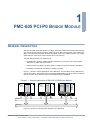
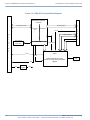
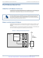
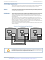
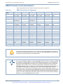
1
Looking for more information?
Visit us on the web at http://www.artisan-scientific.com for more information:
• Price Quotations • Drivers· Technical Specifications. Manuals and Documentation
Artisan Scientific is You~ Source for: Quality New and Certified-Used/Pre:-awned ECJuiflment
• Fast Shipping and DelIve1y
• Tens of Thousands of In-Stock Items
• Equipment Demos
• Hundreds of Manufacturers Supported
• Leasing / Monthly Rentals
Service Center Repairs
Experienced Engineers and Technicians on staff in our
State-of-the-art Full-Service In-House Service Center Facility
• Consignment
InstraView Remote Inspection
Remotely inspect equipment before purchasing with our
Innovative InstraView-website at http://www.instraview.com
We bUy used equipment! We also offer credit for Buy-Backs and Trade-Ins
Sell your excess. underutilized. and idle used equipment. Contact one of our Customer Service Representatives todayl
Talk to a live person: 88EM38-S0URCE fB88-887-68721 I Contact us by email: [email protected] I Visit our website: http://www.artisan-scientific.com
Document Number: 809524
Version: D
Date: February 2009
OUTREACH PCI/PMC
EXPANSION SYSTEM
USER’S MANUAL
Curtiss-Wright Controls Embedded Computing
333 Palladium Drive
Ottawa, Ontario, Canada
K2V 1A6
(613) 599-9199
Artisan Scientific - Quality Instrumentation ... Guaranteed | (888) 88-SOURCE | www.artisan-scientific.com
OUTREACH PCI/PMC EXPANSION SYSTEM USER’S MANUAL
CURTISS-WRIGHT CONTROLS EMBEDDED COMPUTING
REVISION HISTORY
Rev
By
Date
Description
1
-
JL
JL
June 2000
June 2000
A
JP
November 2001
B
JP
June 2002
First engineering release.
Production release.
Updated Appendix B to reflect modified PCI-P0 backplane pins.
Changed cable requirements in Appendix A as product now uses standard basecard cables.
Changed title of document to reflect new tabset.
Added J1 JTAG connector information in Chapter 2.
Updated Chapter 3 to reflect modified PCI-P0 backplane pins.
Changed title of document to reflect new OUTREACH system name.
Improved the explanation on page 1-3 of JTAG support for the CPLD on the
PMC-605.
Clarified statement on page 1-8 to indicate that when the bus is parked, it is parked
on the System Slot.
Changed description of PCI System Reset (RST#) signal on page 2-3 to remove
dependence on the Busmode1 signal.
Removed the Clock Mask section on page 2-4, since the clock signal will now
always be present on the PMC sites (dependence on the Busmode1 signal has
been removed), regardless if a PMC module is installed.
Updated Table 2.6 to reflect pinout changes (signals on P0 connector pins P0-A4
and P0-C4 have been swapped) that were introduced via ECO number
500000000673. This ECO allows smart PMC modules installed on the SVME/DMV210 to perform DMA cycles back to the host card.
Added note on page 3-2 that summarizes which E jumpers on the BPL-605-002 and
BPL-605-003 are reserved.
Improved Figure 3.2, Figure 3.3, and Figure 3.4 to indicate the correct orientation of
the 2 or 3 Slot Development Backplanes and the location of the E-jumper straps.
Corrected errors in Table 3.7 (specifically the descriptions of “Clock Source”,
“Request Line”, and “Grant Line”).
Corrected error in “Configure Master’s Primary BARs” on page 4-9. The Command
Register is located at 0x44, not 0x40 as was previously shown.
C
JP
June 2004
D
JP
February 2009
II
Improved Figure A.3 to clarify how the BPL-605-002 and BPL-605-003 Development Backplane modules need to be oriented for correct operation.
Updated to correct SVME/DMV-210 P0 pinout table (see Table 2.6 on page 2-11).
Updated to correct SVME/DMV-210 P2 pinout table (see Table 2.8 on page 2-13).
Updated to address CR#26124. See “Install PMC-605 on Basecard” on page A-3 for
corrected cross reference to document number 808335.
809524 VERSION D FEBRUARY 2009
Artisan Scientific - Quality Instrumentation ... Guaranteed | (888) 88-SOURCE | www.artisan-scientific.com
CURTISS-WRIGHT CONTROLS EMBEDDED COMPUTING
COPYRIGHT NOTICE
The information in this document is subject to change without notice and should not be
construed as a commitment by Curtiss-Wright Controls, Inc. While reasonable precautions
have been taken, Curtiss-Wright Controls, Inc. assumes no responsibility for any errors that
may appear in this document.
No part of this document may be copied or reproduced without the prior written consent of
Curtiss-Wright Controls, Inc.
The proprietary information contained in this document must not be disclosed to others for
any purpose, nor used for manufacturing purposes, without written permission of CurtissWright Controls, Inc. The acceptance of this document will be construed as an acceptance of
the foregoing condition.
Copyright © 2009, Curtiss-Wright Controls, Inc. All rights reserved.
TRADEMARKS
PowerPC is a trademark of International Business Machines Corporation.
VxWorks is a registered trademark of Wind River Systems, Inc.
Outreach is a trademark of CWCEC Systems Inc.
All other brand and product names are trademarks or registered trademarks of their
respective owners.
809524 VERSION D FEBRUARY 2009
Artisan Scientific - Quality Instrumentation ... Guaranteed | (888) 88-SOURCE | www.artisan-scientific.com
III
OUTREACH PCI/PMC EXPANSION SYSTEM USER’S MANUAL
IV
CURTISS-WRIGHT CONTROLS EMBEDDED COMPUTING
809524 VERSION D FEBRUARY 2009
Artisan Scientific - Quality Instrumentation ... Guaranteed | (888) 88-SOURCE | www.artisan-scientific.com
CURTISS-WRIGHT CONTROLS EMBEDDED COMPUTING
TABLE OF CONTENTS
1. PMC-605 PCI-P0 Bridge Module ................................................................................ 1-1
General Description .............................................................................................................. 1-1
Summary of Features ...................................................................................................... 1-3
PCI-P0 Bridge Description ......................................................................................................1-4
21554 PCI-to-PCI-Bridge Controller ................................................................................... 1-4
Primary and Secondary PCI Buses ..................................................................................... 1-4
PCI-P0 Bus Arbitration ..................................................................................................... 1-5
PCI-P0 Bus Clock ............................................................................................................ 1-6
PCI-P0 System Slot Termination ....................................................................................... 1-8
Interrupts ...................................................................................................................... 1-8
Reset ............................................................................................................................ 1-9
Serial EEPROM.............................................................................................................. 1-10
LED............................................................................................................................. 1-10
Registers ..................................................................................................................... 1-10
Physical, Electrical, and Environmental Characteristics............................................................. 1-11
Dimensions .................................................................................................................. 1-11
Mating Connectors ........................................................................................................ 1-11
Electrical Characteristics ................................................................................................ 1-12
Environmental Characteristics......................................................................................... 1-12
Connector Pin Assignments .................................................................................................. 1-13
Connector Locations ...................................................................................................... 1-13
Pn1/Pn2 Pin Assignments ............................................................................................... 1-14
Pn3 Pin Assignments ..................................................................................................... 1-15
Pn4 Pin Assignments ..................................................................................................... 1-16
J1 Test JTAG Port.......................................................................................................... 1-17
2. SVME/DMV-210 Carrier Card...................................................................................... 2-1
General Description .............................................................................................................. 2-1
Summary of Features ...................................................................................................... 2-2
PCI-P0 Bridge Description ......................................................................................................2-3
Configuration ................................................................................................................. 2-3
PCI Signal Environment ................................................................................................... 2-3
PCI System Reset (RST#) ................................................................................................ 2-3
PCI Interrupts ................................................................................................................ 2-3
PCI JTAG Test Signals...................................................................................................... 2-4
PMC Bus Mode Signals ..................................................................................................... 2-4
Physical, Electrical, and environmental Characteristics ............................................................... 2-5
Dimensions .................................................................................................................... 2-5
Mating Connectors .......................................................................................................... 2-5
Electrical Characteristics .................................................................................................. 2-6
Environmental Characteristics........................................................................................... 2-6
Connector Pin Assignments .................................................................................................... 2-7
PMC Site 1: Jn1 and Jn2 Connectors .................................................................................. 2-7
PMC Site 1: Jn3 and Jn4 Connectors .................................................................................. 2-8
PMC Site 2: Jn1 and Jn2 Connectors .................................................................................. 2-9
PMC Site 2: Jn3 and Jn4 Connectors ................................................................................ 2-10
VME P0 Connector Pin Assignments ................................................................................. 2-11
VME P1 Connector Pin Assignments ................................................................................. 2-12
VME P2 Connector Pin Assignments ................................................................................. 2-13
3. PCI-P0 Development Backplane................................................................................ 3-1
General Description .............................................................................................................. 3-1
Backplane Jumper Configurations ........................................................................................... 3-2
Bus Arbiter Jumper Settings ............................................................................................. 3-2
PCI Bus Clock Jumper Settings ......................................................................................... 3-4
System Slot Termination Jumper Settings .......................................................................... 3-5
809524 REVISION D FEBRUARY 2009
Artisan Scientific - Quality Instrumentation ... Guaranteed | (888) 88-SOURCE | www.artisan-scientific.com
V
OUTREACH PCI/PMC EXPANSION SYSTEM USER’S MANUAL
CURTISS-WRIGHT CONTROLS EMBEDDED COMPUTING
PCI-P0 Backplane Pin Assignments ......................................................................................... 3-7
2 Slot Backplane Configuration Pins .................................................................................. 3-7
2 Slot Backplane System Slot 0 Pin Assignments ................................................................ 3-8
2 Slot Backplane Peripheral Slot 1 Pin Assignments ............................................................. 3-9
3 Slot Backplane Configuration Pins .................................................................................3-10
3 Slot Backplane System Slot 0 Pin Assignments ...............................................................3-11
3 Slot Backplane Peripheral Slot 1 Pin Assignments ............................................................3-12
3 Slot Backplane Peripheral Slot 2 Pin Assignments ............................................................3-13
4. System Integration ......................................................................................................4-1
Configuration of the PCI-P0 Bus ............................................................................................. 4-1
PMC-605 Non-Transparent PCI-PCI Bridging....................................................................... 4-1
SVME/DMV-210 Transparent PCI-PCI Bridging .................................................................... 4-1
PMC-605 Terminology ..................................................................................................... 4-2
Example: Transferring Data Between Two SBCs ....................................................................... 4-3
Serial EEPROM Configuration............................................................................................ 4-3
SVME/DMV-179 GPM Map Command With PMC-605 Installed ............................................... 4-5
Base Address Register Initialization................................................................................... 4-7
Primary BAR Configuration............................................................................................... 4-8
Translated Base Register Configuration.............................................................................. 4-9
Address Map for Local PCI and P0 Buses ...........................................................................4-11
Transferring Data ..........................................................................................................4-11
PCI-P0 Configuration Space Addressing..................................................................................4-12
Addressing Example.......................................................................................................4-12
A. Installation Instructions............................................................................................. A-1
Installation Overview............................................................................................................ A-1
Unpack Cards ................................................................................................................ A-2
Configure Cards and PCI-P0 Development Backplane........................................................... A-2
Install PMC-605 on Basecard............................................................................................ A-3
Insert Cards in Chassis.................................................................................................... A-3
Attach the PCI-P0 Development Backplane......................................................................... A-4
Connect Basecard to Terminal .......................................................................................... A-5
Apply Power .................................................................................................................. A-5
Display Initial Screen Message ......................................................................................... A-5
Install BSP..................................................................................................................... A-6
Index ................................................................................................................................... I-1
VI
809524 REVISION D FEBRUARY 2009
Artisan Scientific - Quality Instrumentation ... Guaranteed | (888) 88-SOURCE | www.artisan-scientific.com
CURTISS-WRIGHT CONTROLS EMBEDDED COMPUTING
LIST OF FIGURES
Figure
Figure
Figure
Figure
Figure
Figure
Figure
Figure
Figure
Figure
Figure
Figure
Figure
Figure
Figure
Figure
Figure
Figure
Figure
Figure
Figure
Figure
Figure
Figure
Figure
Figure
1.1:
1.2:
1.3:
1.4:
1.5:
1.6:
1.7:
1.8:
1.9:
2.1:
2.2:
2.3:
3.1:
3.2:
3.3:
3.4:
4.1:
4.2:
4.3:
4.4:
4.5:
4.6:
4.7:
A.1:
A.2:
A.3:
Sample Application of PMC-605 PCI-P0 Bridge Module............................................... 1-1
PMC-605 Functional Block Diagram ........................................................................ 1-2
Primary and Secondary PCI Buses .......................................................................... 1-4
Bus Arbitration and Signal Direction ....................................................................... 1-5
PCI-P0 Clock Source Configurations ........................................................................ 1-7
Inter-Card Interrupt Mechanism............................................................................. 1-9
PMC-605 Physical Layout .................................................................................... 1-11
Connector Locations ........................................................................................... 1-13
Location of PMC-605 on a SVME/DMV-179............................................................. 1-17
Sample Application of SVME/DMV-210 Carrier Card .................................................. 2-1
SVME/DMV-210 Block Diagram .............................................................................. 2-2
SVME/DMV-210 Physical Layout ............................................................................. 2-5
PCI-P0 Development Backplane Slot Locations (3 Slot Version) .................................. 3-1
Bus Arbiter Jumper Locations ................................................................................ 3-3
Clock Source Jumper Locations .............................................................................. 3-4
Bus Termination Jumper Locations ......................................................................... 3-6
Primary and Secondary PCI Buses .......................................................................... 4-2
Example System .................................................................................................. 4-3
Local PCI Address Map after BAR Configuration ........................................................ 4-7
Example of Address Map based on BAR Requirements ............................................... 4-8
Master-Slave Memory Mappings ........................................................................... 4-11
Type 0 Configuration Cycle Example ..................................................................... 4-13
Type 1 Configuration Cycle Example ..................................................................... 4-13
Outreach PCI/PMC Expansion System .....................................................................A-1
PMC Site Location ................................................................................................A-3
PCI-P0 Backplane Installation ................................................................................A-4
809524 REVISION D FEBRUARY 2009
Artisan Scientific - Quality Instrumentation ... Guaranteed | (888) 88-SOURCE | www.artisan-scientific.com
VII
OUTREACH PCI/PMC EXPANSION SYSTEM USER’S MANUAL
VIII
CURTISS-WRIGHT CONTROLS EMBEDDED COMPUTING
809524 REVISION D FEBRUARY 2009
Artisan Scientific - Quality Instrumentation ... Guaranteed | (888) 88-SOURCE | www.artisan-scientific.com
CURTISS-WRIGHT CONTROLS EMBEDDED COMPUTING
LIST OF TABLES
Table
Table
Table
Table
Table
Table
Table
Table
Table
Table
Table
Table
Table
Table
Table
Table
Table
Table
Table
Table
Table
Table
Table
Table
Table
Table
Table
Table
1.1:
1.2:
1.3:
1.4:
1.5:
1.6:
1.7:
1.8:
2.1:
2.2:
2.3:
2.4:
2.5:
2.6:
2.7:
2.8:
3.1:
3.2:
3.3:
3.4:
3.5:
3.6:
3.7:
3.8:
3.9:
3.10:
4.1:
4.2:
Clock Source Configurations .................................................................................. 1-7
Local Control and Status Register (LCSR) .............................................................. 1-10
Environmental Specification Limits and Ruggedization Levels ................................... 1-12
Pn1/Pn2 Pin Assignments .................................................................................... 1-14
Pn3 Pin Assignments .......................................................................................... 1-15
Pn4 Pin Assignments .......................................................................................... 1-16
J1 Test JTAG Port Pin Assignments ....................................................................... 1-17
Sample SVME/DMV-179 P0 Connector Pin Assignments ........................................... 1-18
Environmental Specification Limits and Ruggedization Levels ..................................... 2-6
PMC Site 1: Pin Assignments (Jn1 and Jn2) ............................................................. 2-7
PMC Site 1: Pin Assignments (Jn3 and Jn4) ............................................................. 2-8
PMC Site 2: Pin Assignments (Jn1 and Jn2) ............................................................. 2-9
PMC Site 2: Pin Assignments (Jn3 and Jn4) ........................................................... 2-10
VME P0 Connector Pin Assignments ...................................................................... 2-11
Pin Assignments for VME P1 Connector ................................................................. 2-12
Pin Assignments for VME P2 Connector ................................................................. 2-13
Bus Arbiter Jumper Settings .................................................................................. 3-3
PCI Bus Clock Jumper Settings .............................................................................. 3-4
System Slot Termination Jumper Settings ............................................................... 3-5
2 Slot Backplane Configuration Pins........................................................................ 3-7
2 Slot Backplane System Slot 0 Pin Assignments ...................................................... 3-8
2 Slot Backplane Peripheral Slot 1 Pin Assignments .................................................. 3-9
3 Slot Backplane Configuration Pins...................................................................... 3-10
3 Slot Backplane System Slot 0 ........................................................................... 3-11
3 Slot Backplane Peripheral Slot 1 ........................................................................ 3-12
3 Slot Backplane Peripheral Slot 2 ........................................................................ 3-13
Serial EEPROM Factory Default Values..................................................................... 4-4
PCI-P0 Configuration Space Address Map .............................................................. 4-12
809524 REVISION D FEBRUARY 2009
Artisan Scientific - Quality Instrumentation ... Guaranteed | (888) 88-SOURCE | www.artisan-scientific.com
IX
OUTREACH PCI/PMC EXPANSION SYSTEM USER’S MANUAL
X
CURTISS-WRIGHT CONTROLS EMBEDDED COMPUTING
809524 REVISION D FEBRUARY 2009
Artisan Scientific - Quality Instrumentation ... Guaranteed | (888) 88-SOURCE | www.artisan-scientific.com
CURTISS-WRIGHT CONTROLS EMBEDDED COMPUTING
PREFACE
PURPOSE
This manual provides an overview of the OUTREACH PCI/PMC Expansion System, which is
comprised of the PMC-605 PCI-P0 Bridge Module, the SVME/DMV-210 Carrier Card, and the
PCI-P0 Development Backplane. The manual also explains how to install the system and
configure the PCI-P0 bus.
AUDIENCE
This document is intended for readers with a technical understanding of hardware engineering
fundamentals, as well as an understanding of the VMEbus, PCI, and CompactPCI
architectures.
SCOPE
This manual contains the following chapters:
Chapter 1 - PMC-605 Bridge Module. Describes the features, functions, and pin
assignments of the PMC-605.
Chapter 2 - SVME/DMV-210 Carrier Card. Describes the features, functions, and pin
assignments of the SVME/DMV-210 Carrier Card.
Chapter 3 - PCI-P0 Development Backplane. Describes the PMC-605’s PCI-P0 2 and 3 slot
development backplanes.
Chapter 4 - System Configuration. Explains how to program the base address registers of
the PMC-605 and lists the default contents of the EEPROM device.
Appendix A - Installation Instructions. Explains how to install the Outreach components
into a system.
RELATED DOCUMENTS
Foundation Firmware v8.0 User’s Manual, CWCEC document #808006. In particular, refer to
Appendix A of this document. It describes the Foundation Firmware extensions specific to the
PMC-605.
Getting Started with the 21554 Embedded PCI-to-PCI Bridge Application Note. Intel
Corporation document #278210-001. Available for download from website at
http://developer.intel.com.
809524 REVISION D FEBRUARY 2009
Artisan Scientific - Quality Instrumentation ... Guaranteed | (888) 88-SOURCE | www.artisan-scientific.com
XI
OUTREACH PCI/PMC EXPANSION SYSTEM USER’S MANUAL
CURTISS-WRIGHT CONTROLS EMBEDDED COMPUTING
CONVENTIONS USED IN THIS MANUAL
This document and the accompanying documents in the documentation package use various
icon conventions and abbreviations to make the documents clearer and easier to read. These
conventions cover typography for such elements as sample software code and keystrokes,
signal meanings, and graphical elements for important information such as warnings or
cautions.
Typographic
Conventions
Table 1 lists the typographical conventions used in documents contained in this documentation
package.
TABLE 1: Typographical Conventions
Item
Convention
Example
Keystrokes
Keys are listed as they appear on most keyboards,
surrounded by < > marks. Combinations of keystrokes appear within a single set of < > brackets.
File names are set in italics.
Directory names show the full directory path. The last
directory in the path does not have a trailing slash
following it.
Prompts and other text appearing on monitors is set
in bold monospace type.
Firmware code, and any information you need to
type in response to a prompt, is set in monospace
type.
Type < Ctrl-Alt-C > to return to the previous menu.
Type < Esc > to exit.
File Names
Directory Names
Monitor Displays
Firmware Code
Signal
Conventions
Open the file named es.h.
Go to the c:\windows\temp\backup directory.
% mpp MC68040gnu >
% make -f Makefile.MC68040gnu
Table 2 lists symbols that can follow a signal name. For example, the asterisk (#) is used with
a PCI signal name, such as IRDY#.
TABLE 2: Signal Conventions
XII
Symbol
Description
[no symbol]
# or -
The signal is active HIGH.
The signal is active LOW.
809524 REVISION D FEBRUARY 2009
Artisan Scientific - Quality Instrumentation ... Guaranteed | (888) 88-SOURCE | www.artisan-scientific.com
CURTISS-WRIGHT CONTROLS EMBEDDED COMPUTING
Abbreviations
Table 3 lists the abbreviations used to describe the size of a memory device or a range of
addresses.
TABLE 3: Abbreviations
Abbreviation
Convention
1 Kbyte
1 Mbyte
1 Gbyte
1,024 bytes
1,024 Kbytes
1,024 Mbytes
Memory
Addresses
Unless otherwise stated, all memory addresses are shown in hexadecimal notation.
Icons
The following icons are used throughout this document:
Cross Reference
Warning
Caution
Cross references to other documents are used when a subject being discussed is addressed
in depth by another, more authoritative document. Cross references are also used for
document chapters and sections.
The warning icon indicates procedures in the manual that, if not carried out, or if carried out
incorrectly, could cause physical injury, electrical damage to equipment, or a nonrecoverable corruption of data. Warnings include instructions for preventing such damage.
Please observe warning icons and read the accompanying text completely before carrying
out the procedure.
The caution icon indicates non-catastrophic incidents, complex practices, or procedures
which, if not observed, could result in damage to the hardware. Cautions include specific
instructions for avoiding or minimizing these incidents.
The note icon highlights exceptions and special information.
Note
Tips provide extra information on the subject matter. This could include hints about how to
use your current CWCEC card to its maximum potential.
Tip
809524 REVISION D FEBRUARY 2009
Artisan Scientific - Quality Instrumentation ... Guaranteed | (888) 88-SOURCE | www.artisan-scientific.com
XIII
OUTREACH PCI/PMC EXPANSION SYSTEM USER’S MANUAL
CURTISS-WRIGHT CONTROLS EMBEDDED COMPUTING
TECHNICAL SUPPORT INFORMATION
If you are unable to resolve installation or configuration-related difficulties using the guidance
provided in this document, contact Technical Support or check out the Continuum Support
Center web site for additional assistance:
http://csc.cwcembedded.com/
Once registered, you will have online access to additional or updated technical documentation,
in addition to software components, etc. as these items become available.
To Access CWCEC
Technical Support
For Technical Support contact information, go to the CWCEC web site:
http://www.cwcembedded.com/
and click on the “Contact” tab. This will bring up a page containing links specific to your needs:
http://www.cwcembedded.com/1/88/61.html
From here you can access additional topics such as :
Repair and
Warranty
Information
•
Continuum Lifecycle Services
•
Technical Support
•
Professional Services
•
Interoperability
•
Repair and Warranty
•
Software Upgrade Program
•
Lifecycle Support
Curtiss-Wright Controls Embedded Computing’s standard warranty provides one-year
coverage of parts and labor and also features:
•
A repair turnaround target of 15 business days
•
Return shipping
•
No-fault-found coverage
•
Quality Engineering services such as corrective repair reporting and failure analysis
when warranted
Repairs outside the scope of the warranty are performed for a fixed price for in-production
cards. Fixed prices help customers achieve cost determinism and, through streamlined
administration associated with fixed prices, shorten repair turn-around times.
To obtain and prepare a Return Material Authorization (RMA) form, click on the “Repair &
Warranty” link available on the Tech Support Contact page identified above.
XIV
809524 REVISION D FEBRUARY 2009
Artisan Scientific - Quality Instrumentation ... Guaranteed | (888) 88-SOURCE | www.artisan-scientific.com
1
PMC-605 PCI-P0 BRIDGE MODULE
GENERAL DESCRIPTION
The PMC-605 PCI-P0 Bridge Module is a single-width PMC module that extends the local PCI
bus of its host Single Board Computer (SBC) out to the SBC’s P0 connector. This enables the
SBC to communicate with other similarly equipped cards in the VMEbus system over a highspeed PCI bus (referred to as the PCI-P0 bus in this manual).
The PMC-605 performs such functions as:
•
Expanding the number of PMC modules attached to a processor card (single board
computer or digital signal processor)
•
Interconnecting multiple processor cards via a high-speed PCI secondary backplane.
•
Providing a private PCI data path to custom I/O cards.
Figure 1.1 shows a sample application of the PMC-605. The two SBCs use the PMC-605 to
access each others’ shared PCI resources while the SVME/DMV-210 Carrier Card extends the
PCI bus of each single board computer with additional I/O capabilities.
Single
Board
Computer
PMC-605
Single
Board
Computer
PMC-605
Custom
I/O Card
Custom
I/O Card
SVME/DMV-210
Carrier Card
FIGURE 1.1: Sample Application of PMC-605 PCI-P0 Bridge Module
VMEbus
PCI-P0 Bus
Figure 1.2 shows a functional block diagram of the PMC-605.
809524 REVISION D FEBRUARY 2009
Artisan Scientific - Quality Instrumentation ... Guaranteed | (888) 88-SOURCE | www.artisan-scientific.com
1-1
OUTREACH PCI/PMC EXPANSION SYSTEM USER’S MANUAL
CURTISS-WRIGHT CONTROLS EMBEDDED COMPUTING
FIGURE 1.2: PMC-605 Functional Block Diagram
Intel 21554
Embedded PCI Bridge
Controller
Secondary PCI Bus
Secondary
Bus
Primary Bus
P
C
I
PCI Int
H
o
s
t
P
C
I
P
0
Primary PCI Bus
Arbiter Functions
Configuration Settings
Serial EEPROM
(Bridge
Configuration)
Control
B
u
s
Pri D'bell Int
B
u
s
CPLD
PCI Int
JTAG
JTAG
+5V
1-2
3.3V
Regulator
System Controller Functions,
Arbiter and Local Control and Status
Register
Status
LED
+3.3V
809524 REVISION D FEBRUARY 2009
Artisan Scientific - Quality Instrumentation ... Guaranteed | (888) 88-SOURCE | www.artisan-scientific.com
CURTISS-WRIGHT CONTROLS EMBEDDED COMPUTING
PMC-605 PCI-P0 BRIDGE MODULE
SUMMARY OF FEATURES
The PMC-605 has the following major features:
Clock Speed
The Intel 21554 PCI-to-PCI Bridge device supports a clock speed of 33 MHz on the Secondary
PCI Bus and 33 MHz on the Primary PCI bus. The Primary PCI bus connects to the PCI-P0
bus and the Secondary PCI bus interface connects to the Host PCI bus.
Bus Arbitration
The PMC-605 is dynamically configured during power-up or reboot to act as the bus arbiter
when placed in the PCI-P0 backplane’s System Slot. The PMC-605 uses a parallel arbitration
scheme.
PCI Bus Clock
The PMC-605 can generate a PCI bus clock for the PCI-P0 bus or receive it from an external
source. The PCI bus clock is dynamically enabled when placed in the PCI-P0 backplane’s
System Slot and is disabled when placed in a Peripheral Slot.
Synchronous and
Asynchronous
Operation
The PCI-P0 bus can be synchronous to the Primary PCI bus or operate completely
asynchronously according to the configuration of its PCI bus clock source.
System Slot
Termination
The PMC-605 is dynamically configured during power-up or reboot to terminate signals as
necessary for the PCI bus when placed in the PCI-P0 backplane’s System Slot.
Power
Requirements
The PCI-P0 bus is 3.3 V signalling, 5 V tolerant. The PMC-605 is powered via the basecard’s
+5 V rail; an on-board regulator provides +3.3 V.
Configuration
EEPROM
A serial EEPROM stores basic configuration information for the 21554
PCI-to-PCI Bridge device.
JTAG Support
The CPLD supports the IEEE Std 1149.1 boundary scan (JTAG) and is In-System
Programmable (if so configured by the fitting of optional zero ohm resistors) through the
host SBC JTAG interface. If the optional zero ohm resistors are not fitted, the CPLD must be
programmed through an on-board header. Note that the Intel 21554 is not included as part
of the JTAG loop.
Ruggedization
Levels
The PMC-605 is available in air-cooled and conduction-cooled versions.
LED
The PMC-605 has a green software-controllable power-on LED.
More information on the PMC-605 features listed above is provided in the following sections.
Note
809524 REVISION D FEBRUARY 2009
Artisan Scientific - Quality Instrumentation ... Guaranteed | (888) 88-SOURCE | www.artisan-scientific.com
1-3
OUTREACH PCI/PMC EXPANSION SYSTEM USER’S MANUAL
CURTISS-WRIGHT CONTROLS EMBEDDED COMPUTING
PCI-P0 BRIDGE DESCRIPTION
21554 PCI-TO-PCI-BRIDGE CONTROLLER
The PMC-605 uses the Intel 21554 Embedded PCI-to-PCI Bridge device. The 21554 is a nontransparent PCI-to-PCI bridge designed to connect multiple processor domains, enabling the
host basecard to independently configure and control the local subsystem.
Cross Reference
The 21554 responds to Type 0 configuration cycles. For information about this device refer
to the Intel’s Getting Started with the 21554 Embedded PCI-to-PCI Bridge Application
Note, document #278210-001. Manuals and data sheets on the 21554 can be downloaded
from Intel’s website at http://developer.intel.com.
PRIMARY AND SECONDARY PCI BUSES
The PMC-605’s Primary PCI bus runs through the P4 connector to the P0 connector on the
basecard. The Primary PCI bus runs at 33 MHz and supports 32-bit addressing and data
transfers.
The Secondary PCI bus is connected to the host basecard’s local PCI bus. The Secondary PCI
bus runs at 33 MHz and supports 64-bit addressing and data transfers.
FIGURE 1.3: Primary and Secondary PCI Buses
PMC-605
Module
Pn1
Pn2
VME
Backplane
(PCI-P0 bus)
PCI Bridge
Secondary PCI Bus
(Local Host PCI Bus)
Pn3
Primary PCI Bus
1-4
Pn4
Host
Basecard
P0
809524 REVISION D FEBRUARY 2009
Artisan Scientific - Quality Instrumentation ... Guaranteed | (888) 88-SOURCE | www.artisan-scientific.com
CURTISS-WRIGHT CONTROLS EMBEDDED COMPUTING
PMC-605 PCI-P0 BRIDGE MODULE
PCI-P0 BUS ARBITRATION
The PMC-605 can act as the bus arbiter for the PCI-P0 bus. A CPLD provides the arbitration
functions; the arbitration functions built into the 21554 bridge chip are not used.
Arbitration
Scheme
The PMC-605 uses a parallel arbitration scheme in which each card on the PCI-P0 bus is free
to request the use of the bus at any time. The PMC-605 acting as bus arbiter grants the bus
on a “first come, first serve” basis.
PCI-P0 Bus Arbiter
Enable/Disable
The PMC-605 acts as the PCI-P0 bus arbiter when the ARBDIS signal is connected directly to
Ground. When the arbiter function is enabled, REQ0# and REQ1# signals are inputs to the
arbiter, signalling that the asserting device requests the use of the PCI-P0 bus. After
completing the arbitration process, the arbiter asserts the GNT0# or GNT1# signal to the
requesting device.
The PMC-605’s arbiter function is disabled when the ARBDIS signal is connected to Vcc.
When the arbiter function is disabled, the role of REQ0# and GNT0# become reversed. The
REQ0# pin functions as GNT0# (i.e. becomes the Grant 0 input) and the GNT0# pin
functions as REQ0# (i.e. becomes the Request 0 output). In other words, REQn# signals are
always inputs and GNTn# signals are always outputs.
Figure 1.4 illustrates the function of each signal when the PMC-605’s arbiter function is either
enabled or disabled.
FIGURE 1.4: Bus Arbitration and Signal Direction
System Slot 0
Peripheral Slot 1
Peripheral Slot 2
PMC-605
PMC-605
PMC-605
21554
GNT1#
Arbiter Disabled
REQ1#
Arbiter/
Requester
GNT
GNT1#
GNT0#
REQ0#
Arbiter Disabled
(ARBDIS connected to Vcc)
REQ1#
Arbiter/
Requester
GNT
GNT1#
REQ1#
GNT0#
Arbiter Enabled
REQ0#
GNT
(ARBDIS connected to GND)
REQ
REQ
Arbiter/
Requester
GNT0#
REQ
21554
REQ0#
21554
(ARBDIS connected to Vcc)
Grant from Enabled Arbiter
Request to Enabled Arbiter
Grant from Enabled Arbiter
Request to Enabled Arbiter
The ARBDIS signal must not be left open circuit because it is an input to the arbiter device
which does not have a pull-up on it. Inputs should not be left floating. Also note that only
one card in the system should be configured as the bus arbiter.
Caution
809524 REVISION D FEBRUARY 2009
Artisan Scientific - Quality Instrumentation ... Guaranteed | (888) 88-SOURCE | www.artisan-scientific.com
1-5
OUTREACH PCI/PMC EXPANSION SYSTEM USER’S MANUAL
Cross Reference
CURTISS-WRIGHT CONTROLS EMBEDDED COMPUTING
Refer to “Bus Arbiter Jumper Settings” on page 3-2 for information on configuring arbiter
settings when using the PMC-605 with the PCI-P0 Development Backplane (part number
BPL-605-002 or BPL-605-003).
PCI-P0 BUS CLOCK
The PMC-605 functions as the PCI-P0 bus clock source when the CLKDIS signal is connected
directly to Ground. The PMC-605 provides a 33 MHz clock source on both SCLK0 and SCLK1.
The PCI-P0 bus clock source is disabled when the CLKDIS signal is connected directly to Vcc.
In this mode the PCI-P0 bus clock needs to be provided from an external source (such as
from a basecard’s 33 MHz clock or another PMC-605). The PCI-P0 clock source is always
received on PCLK0. PCLK1 is only used in systems with more than three slots on the PCI-P0
bus.
Cross Reference
The CLKDIS signal referred to above is connected to Ground or Vcc via the 2 or 3 slot PCIP0 Development Backplane (part number BPL-605-002 or BPL-605-003). See “PCI Bus
Clock Jumper Settings” on page 3-4 for details.
The state of the PMC-605’s arbiter function has no affect on clock selection.
CLKDIS must not be left open circuit because it is an input to the CPLD which does not have
a pull-up on it. Inputs should not be left floating. The PMC-605 may not be detected by
the host processor if this line is left open.
Caution
1-6
Also note that there should be only one card on the PCI-P0 bus that provides the clock
source.
809524 REVISION D FEBRUARY 2009
Artisan Scientific - Quality Instrumentation ... Guaranteed | (888) 88-SOURCE | www.artisan-scientific.com
CURTISS-WRIGHT CONTROLS EMBEDDED COMPUTING
PMC-605 PCI-P0 BRIDGE MODULE
PCI-P0 Clock
Source
Configurations
Table 1.1 and Figure 1.5 describe the different clock source configurations possible with the
PMC-605 in a two or three slot backplane configuration.
TABLE 1.1:
Clock Source Configurations
Configuration
Description
Fully Synchronous Clock System Slot
The PMC-605 in the system slot receives a 33 MHz clock source from its host card
and routes it over the PCI-P0 bus to the other PMC-605s. In this configuration, the bus
clock source is disabled for all PMC-605s in the system. The primary and secondary
buses of each PMC-605 module operate at the same clock speed.
Asynchronous System Slot
The PMC-605 in the system slot receives a 33 MHz clock source from its host card to
provide timing for its secondary side. The PMC-605’s primary bus uses a clock source
generated by its on-board oscillator (see Note) and routes this second clock over the
PCI-P0 bus. In this configuration, the primary and secondary sides can operate at different clock speeds.
Peripheral Slot
PMC-605 modules in the peripheral slots receive clocking from their host cards for
their secondary sides. Their primary buses use a clock source on the PCI-P0 bus.
Note:
The on-board oscillator is not installed on standard versions of the PMC-605 product. Consult
the factory if you require a version of the product that includes the oscillator.
FIGURE 1.5: PCI-P0 Clock Source Configurations
Asynchronous
System Slot
Fully Synchronous
System Slot
PCI Clock
PCI Clock
21554
CLK0
CLK0
CLK0
OSC.
0-33 MHz
Primary PCI Bus
Primary PCI Bus
CLK0
CLK0
PCI-P0 Bus
Secondary PCI Bus
Secondary PCI Bus
Buffer
CLK0
21554
21554
Secondary PCI Bus
Primary PCI Bus
Host PCI Bus
Host PCI Bus
Host PCI Bus
PCI Clock
Peripheral Slot
PCI-P0 Bus
PCI-P0 Bus
809524 REVISION D FEBRUARY 2009
Artisan Scientific - Quality Instrumentation ... Guaranteed | (888) 88-SOURCE | www.artisan-scientific.com
1-7
OUTREACH PCI/PMC EXPANSION SYSTEM USER’S MANUAL
CURTISS-WRIGHT CONTROLS EMBEDDED COMPUTING
PCI-P0 SYSTEM SLOT TERMINATION
The PMC-605 terminates signals as required for a PCI System Slot Controller when the
TERMDIS signal is connected directly to Ground. The System Slot termination is disabled
when the TERMDIS signal is connected directly to Vcc.
Cross Reference
The TERMDIS signal referred to above is connected to Ground or Vcc via the 2 or 3 slot PCIP0 Development Backplane (part number BPL-605-002 or BPL-605-003). The PMC-605
terminates signals when placed in the PCI-P0 backplane’s System Slot. It does not
terminate signals when placed in a Peripheral Slot. See “System Slot Termination Jumper
Settings” on page 3-5 of this manual for information on configuring signal termination
settings when using the PMC-605 with the PCI-P0 Development Backplane.
The term System Slot Controller refers to a PMC-605 when it is configured to provide PCI
bus arbitration on the PCI-P0, distribute the PCI Bus clock across the backplane, and provide
termination of specific signals.
In a multi-slot system, the bus is normally 'parked' on the System slot by the arbiter when
the arbiter assigns a card default ownership of the bus. This ensures that the majority of the
signals on the bus are driven but reduces power requirements by removing the necessity of
each card having pull-ups. Some signals, however, need to be free for any card to assert.
These signals cannot be left floating or driven and hence the System Controller provides the
pull-ups (terminations) for these signals. On the PMC-605 these signals are: FRAME, TRDY,
IRDY, DEVSEL, STOP, SERR, PERR and INTA.
The TERMDIS signal must not be left open circuit because it is an input to the CPLD which
does not have a pull-up on it. Inputs should not be left floating.
Caution
INTERRUPTS
The 21554 PCI-to-PCI Bridge device does not accept interrupts although it may generate
them to either the primary bus (P0 side) or secondary bus (host processor side). Any P0 bus
interrupt is seen directly by the basecard, as long as bit D5 of the LCSR is set to a '1' - if bit
D5 of the LCSR is set to a '0' (default), then the P0 bus interrupt is withheld from the
basecard.
Interrupts are passed between processor cards using “doorbell” registers in the 21554.
Interrupts from non-intelligent cards use the INT line on the PCI-P0 bus and are buffered
through the PMC-605 card to the host processor card.
1-8
809524 REVISION D FEBRUARY 2009
Artisan Scientific - Quality Instrumentation ... Guaranteed | (888) 88-SOURCE | www.artisan-scientific.com
CURTISS-WRIGHT CONTROLS EMBEDDED COMPUTING
PMC-605 PCI-P0 BRIDGE MODULE
FIGURE 1.6: Inter-Card Interrupt Mechanism
System Slot 0
Basecard
Peripheral Slot 1
Basecard
INTA#
Basecard
INTA#
PMC-605
INTA#
PMC-605
21554
CPLD
INTA#
Peripheral Slot 2
PMC-605
21554
CPLD
INTA#
21554
CPLD
INTA#
PCI-P0 Bus
Generating PCI-P0
Bus Interrupts
The PMC-605 can generate an interrupt on PCI-P0 bus (INTA#) using the doorbell registers
in the 21554. This interrupt is routed to INTA# on the host PCI bus.
Inter-card Interrupt
Mechanism
The PMC-605 uses the 21554 Secondary Interrupt Request register to assert INTA# on the
host PCI bus. This provides an inter-card interrupt mechanism directly under software
control.
Cross Reference
The PCI-P0 INTA# to the host PCI bus is enabled and disabled by a software-controllable bit
in the PMC-605’s Local Control and Status Register (LCSR). Refer to page 1-10 for
information on the LCSR.
RESET
Only a card with TERMDIS grounded can generate a PCI-P0 Reset. It can either follow the
Reset signal from the host or it can be initiated from the host through software.
The PMC-605 does not accept resets from the PCI-P0 bus, regardless of the state of
TERMDIS. If an external PMC-605 reset is required, this must be done via the host
basecard’s VME interface.
809524 REVISION D FEBRUARY 2009
Artisan Scientific - Quality Instrumentation ... Guaranteed | (888) 88-SOURCE | www.artisan-scientific.com
1-9
OUTREACH PCI/PMC EXPANSION SYSTEM USER’S MANUAL
CURTISS-WRIGHT CONTROLS EMBEDDED COMPUTING
SERIAL EEPROM
A serial EEPROM provides basic configuration details to the 21554
PCI-to-PCI Bridge device such as subsystem vendor ID (“D4D4”) and subsystem device ID
(“0605”). The configuration details can be programmed by the host card and read by the
21554 after power-up or card reset. Refer to Chapter 4 of this manual and Appendix A of the
V8 Foundation Firmware User’s Manual (808006) for more information.
LED
The PMC-605 has a green power-on LED that is software-controllable via the Local Control
and Status Register (LCSR). After Power up or reset, the LED will be initially illuminated. The
LED is extinguished when the PMC605 is successfully initialized and its diagnostics passed
by FF/W.
REGISTERS
The Local Control and Status Register (LCSR) is a byte-wide register residing within the
address space defined by the PCI Expansion ROM Base Address set within the 21554 PCI-toPCI Bridge device.
The bit definitions of the LCSR are as described in Table 1.2.
TABLE 1.2:
Local Control and Status Register (LCSR)
D7
D6
D5
D4
D3
D2
D1
D0
Not Used
Not Used
Host INTA#
Enable
LED Control
Arbiter Mode
Arbiter
Status
Clock Source
Termination Status
Bit
Name
Description
R/W
@ Reset
D7
N/A
N/A
X
X
D6
N/A
N/A
X
X
D5
Host INTA# Enable
1 = Host INTA# is enabled
0 = Host INTA# is disabled
R/W
0
D4
LED Control
1 = LED On
0 = LED Off
R/W
1
D3
Arbiter Mode
1 = Serial Arbitration
0 = Parallel Arbitration
R
As per backplane
configuration
D2
Arbiter Status
1 = Arbiter Disabled
0 = Arbiter Enabled
R
As per backplane
configuration
D1
Clock Source
1 = Clock Source Disabled
0 = Clock Source Enabled
R
As per backplane
configuration
D0
Termination Status
1 = Termination Disabled
0 = Termination Enabled
R
As per backplane
configuration
1-10
809524 REVISION D FEBRUARY 2009
Artisan Scientific - Quality Instrumentation ... Guaranteed | (888) 88-SOURCE | www.artisan-scientific.com
CURTISS-WRIGHT CONTROLS EMBEDDED COMPUTING
PMC-605 PCI-P0 BRIDGE MODULE
PHYSICAL, ELECTRICAL, AND ENVIRONMENTAL
CHARACTERISTICS
Figure 1.7 shows the location of the major components and the mating connectors on the
PMC-605.
FIGURE 1.7: PMC-605 Physical Layout
Component Side
Solder Side
J1
21554
CPLD
Pn1
Pn3
Pn2
Pn4
DIMENSIONS
The PMC-605 is built on a standard PCI Mezzanine Card (PMC) Printed Wiring Board (PWB)
and is VITA 20 compliant.
MATING CONNECTORS
The connectors Pn1, Pn2, Pn3, and Pn4 are compliant with IEEE P1386.
809524 REVISION D FEBRUARY 2009
Artisan Scientific - Quality Instrumentation ... Guaranteed | (888) 88-SOURCE | www.artisan-scientific.com
1-11
OUTREACH PCI/PMC EXPANSION SYSTEM USER’S MANUAL
CURTISS-WRIGHT CONTROLS EMBEDDED COMPUTING
ELECTRICAL CHARACTERISTICS
The PMC-605 is powered from the basecard’s +5 V rail and operates with a steady state input
voltage of 5.0 +/- 0.25 volts DC with a maximum current of 0.75 A. It draws less than 4
watts of power. An on-board regulator provides +3.3 V for the 21554 PCI to PCI Bridge
device. The PMC-605 does not require + 3.3 V from its host basecard.
ENVIRONMENTAL CHARACTERISTICS
Table 1.3 shows the complete range of environmental specification limits used to categorize
the ruggedization levels of CWCEC products. The PMC-605 is available in ruggedization levels
0 and 200.
TABLE 1.3:
Card
Environmental Specification Limits and Ruggedization Levels
Operating
Temperature
Storage
Operating
Temperature Humidity
Storage
Humidity
Sine
Vibration
(note 1)
Random
Vibration
Mechanical
Shock
(note 4)
(note 5)
Air-Cooled
Level 0
0°C to 50°C
inlet 4 cfm air
flow (note 6)
-40°C to 85°C
0 to 95%
0 to 95%
N/A
non-condensing non-condensing
N/A
N/A
Air-Cooled
Level 50
-20°C to 65°C
inlet 4 cfm air
flow (note 6)
-40°C to 85°C
0 to 100%
0 to 100%
N/A
non-condensing non-condensing
0.02 g2/Hz
20-2000 Hz
30 g peak
half sine
pulse
11 ms duration
Air-Cooled
Level 100
-40°C to 71°C
inlet 4 cfm air
flow (note 6)
-55°C to 85°C
0 to 100%
0 to 100%
10 g peak
non-condensing non-condensing 15-2000 Hz
0.04 g2/Hz
15-2000 Hz
30 g peak
half sine
pulse
11 ms duration
ConductionCooled
Level 100
-40°C to 71°C
card edge
temperature
-55°C to 85°C
0.01 g2/Hz
15-2000 Hz
40 g peak
half sine
pulse
11 ms duration
ConductionCooled
Level 200
-55°C to 85°C
card edge
temperature
-62°C to 125°C 0 to 100%
0 to 100%
non-condensing condensing
0.1 g2/Hz
15-2000 Hz
40 g peak
half sine
pulse
11 ms duration
(note 2)
0 to 100%
0 to 100%
10 g
non-condensing non-condensing 15-2000 Hz
(note 3)
10 g
15-2000 Hz
(note 3)
Notes
1. All levels based on a sweep duration of ten minutes per axis, each of three mutually
perpendicular axis.
2. Displacement limited to 0.10 inches D.A. from 15 to 44 Hz.
3. Displacement limited to 0.436 inches D.A. from 15 to 21 Hz.
4. 60 minutes per axis each of three mutually perpendicular axes.
5. Three hits per direction per axis (total of 18 hits).
6. At sea level.
1-12
809524 REVISION D FEBRUARY 2009
Artisan Scientific - Quality Instrumentation ... Guaranteed | (888) 88-SOURCE | www.artisan-scientific.com
CURTISS-WRIGHT CONTROLS EMBEDDED COMPUTING
PMC-605 PCI-P0 BRIDGE MODULE
CONNECTOR PIN ASSIGNMENTS
CONNECTOR LOCATIONS
The locations of the Pn1, Pn2, Pn3, Pn3 and J1 connectors are shown in
Figure 1.8.
FIGURE 1.8: Connector Locations
J1
Pn1
Pn3
Pn2
Pn4
809524 REVISION D FEBRUARY 2009
Artisan Scientific - Quality Instrumentation ... Guaranteed | (888) 88-SOURCE | www.artisan-scientific.com
1-13
OUTREACH PCI/PMC EXPANSION SYSTEM USER’S MANUAL
CURTISS-WRIGHT CONTROLS EMBEDDED COMPUTING
PN1/PN2 PIN ASSIGNMENTS
TABLE 1.4:
Pn1/Pn2 Pin Assignments
Pn1 32-bit PCI
Pn2 32-bit PCI
Pin #
Signal Name
Signal Name
Pin #
Pin #
Signal Name
Signal Name
Pin #
1
TCK
-12V
2
1
+12V
TRST#
2
3
Ground
INTA#
4
3
TMS
TDO
4
5
INTB#
INTC#
6
5
TDI
Ground
6
7
BUSMODE1#
+5V
8
7
Ground
PCI-RSVD*
8
9
INTD#
PCI-RSVD*
10
9
PCI-RSVD*
PCI-RSVD*
10
11
Ground
PCI-RSVD*
12
11
BUSMODE2#
+3.3V
12
13
CLK
Ground
14
13
RST#
BUSMODE3#
14
15
Ground
GNT#
16
15
3.3V
BUSMODE4#
16
17
REQ#
+5V
18
17
PCI-RSVD*
Ground
18
19
V (I/O)
AD[31]
20
19
AD[30]
AD[29]
20
21
AD[28]
AD[27]
22
21
Ground
AD[26]
22
23
AD[25]
Ground
24
23
AD[24]
+3.3V
24
25
Ground
C/BE[3]#
26
25
IDSEL
AD[23]
26
27
AD[22]
AD[21]
28
27
+3.3V
AD[20]
28
29
AD[19]
+5V
30
29
AD[18]
Ground
30
31
V(I/O)
AD[17]
32
31
AD[16]
C/BE[2]#
32
33
FRAME#
Ground
34
33
Ground
PMC-RSVD
34
35
Ground
IRDY#
36
35
TRDY#
+3.3V
36
37
DEVSEL#
+5V
38
37
Ground
STOP#
38
39
Ground
LOCK#
40
39
PERR#
Ground
40
41
SDONE#
SBO#
42
41
+3.3V
SERR#
42
43
PAR
Ground
44
43
C/BE[1]#
Ground
44
45
V(I/O)
AD[15]
46
45
AD[14]
AD[13]
46
47
AD[12]
AD[11]
48
47
Ground
AD[10]
48
49
AD[09]
+5V
50
49
AD[08]
+3.3V
50
51
Ground
C/BE[0]#
52
51
AD[07]
PMC-RSVD
52
53
AD[06]
AD[05]
54
53
+3.3V
PMC-RSVD
54
55
AD[04]
Ground
56
55
PMC-RSVD
Ground
56
57
V(I/O)
AD[03]
58
57
PMC-RSVD
PMC-RSVD
58
59
AD[02]
AD[01]
60
59
Ground
PMC-RSVD
60
61
AD[00]
+5V
62
61
ACK64#
+3.3V
62
63
Ground
REQ64#
64
63
Ground
PMC-RSVD
64
1-14
809524 REVISION D FEBRUARY 2009
Artisan Scientific - Quality Instrumentation ... Guaranteed | (888) 88-SOURCE | www.artisan-scientific.com
CURTISS-WRIGHT CONTROLS EMBEDDED COMPUTING
PMC-605 PCI-P0 BRIDGE MODULE
PN3 PIN ASSIGNMENTS
TABLE 1.5:
Pn3 Pin Assignments
Pin #
Signal Name
Signal Name
Pin #
1
PCI-RSVD
GND
2
3
GND
CBE7#
4
5
CBE6#
CBE5#
6
7
CBE4#
GND
8
9
V(I/O)
PAR64
10
11
AD[63]
AD[62]
12
13
AD[61]
GND
14
15
GND
AD[60]
16
17
AD[59]
AD[58]
18
19
AD[57]
GND
20
21
V(I/O)
AD[56]
22
23
AD[55]
AD[54]
24
25
Ad[53]
GND
26
27
GND
AD[52]
28
29
AD[51]
AD[50]
30
31
AD[49]
GND
32
33
GND
AD[48]
34
35
AD[47]
AD[46]
36
37
AD[45]
GND
38
39
V(I/O)
AD[44]
40
41
AD[43]
AD[42]
42
43
AD[41]
GND
44
45
GND
AD[40]
46
47
AD[39]
AD[38]
48
49
AD[37]
GND
50
51
GND
AD[36]
52
53
AD35
AD34
54
55
AD33
GND
56
57
V(I/O)
AD32
58
59
PCI-RSVD
PCI-RSVD
60
61
PCI-RSVD
GND
62
63
GND
PCI-RSVD
64
809524 REVISION D FEBRUARY 2009
Artisan Scientific - Quality Instrumentation ... Guaranteed | (888) 88-SOURCE | www.artisan-scientific.com
1-15
OUTREACH PCI/PMC EXPANSION SYSTEM USER’S MANUAL
CURTISS-WRIGHT CONTROLS EMBEDDED COMPUTING
PN4 PIN ASSIGNMENTS
TABLE 1.6:
1-16
Pn4 Pin Assignments
Pin #
Signal Name
Signal Name
Pin #
1
RST#
PCLK0
2
3
REQ0#
GND
4
5
GNT0#
INTA#
6
7
GND
PCLK1
8
9
REQ1#
DEVSEL#
10
11
GNT1#
SERARB
12
13
IRDY#
TRDY#
14
15
+5 V
SERR#
16
17
IDSEL
PERR#
18
19
STOP#
TERMDIS
20
21
PAR
FRAME#
22
23
CLOCKDIS
CBE3
24
25
CBE2
CBE0
26
27
CBE1
ARBDIS
28
29
AD0
AD1
30
31
AD2
AD3
32
33
AD4
AD5
34
35
GND
AD7
36
37
AD6
AD9
38
39
AD8
AD11
40
41
AD10
AD13
42
43
AD12
GND
44
45
AD14
AD15
46
47
AD16
AD17
48
49
AD18
AD19
50
51
GND
AD21
52
53
AD20
AD23
54
55
AD22
AD25
56
57
AD24
AD27
58
59
AD26
GND
60
61
AD28
AD29
62
63
AD30
AD31
64
809524 REVISION D FEBRUARY 2009
Artisan Scientific - Quality Instrumentation ... Guaranteed | (888) 88-SOURCE | www.artisan-scientific.com
CURTISS-WRIGHT CONTROLS EMBEDDED COMPUTING
PMC-605 PCI-P0 BRIDGE MODULE
J1 TEST JTAG PORT
TABLE 1.7:
SVME/DMV-179
SBC P0 Pin
Assignments
J1 Test JTAG Port Pin Assignments
Pin
Signal
1
TCK (Xilinx & Bridge)
2
TDI (Xilinx)
3
TMS (Xilinx & Bridge)
4
TDO (Xilinx - connects to TDI of Bridge)
5
+5 V
6
RST (Bridge)
7
TDO (Bridge)
On an SVME/DMV-179 Single Board Computer, the PMC-605 would typically be installed in
the PMC1 interface in order to access the 179’s P0 connector.
FIGURE 1.9: Location of PMC-605 on a SVME/DMV-179
SVME/DMV-179
P1
PMC-605
P0
P2
Table 1.8 describes the P0 connector of an SVME/DMV-179 with a PMC-605 mounted in the
PMC1 interface. The shaded boxes represent PCI signals provided by the PMC-605 when
plugged into the System Slot on the PCI-P0 backplane.
809524 REVISION D FEBRUARY 2009
Artisan Scientific - Quality Instrumentation ... Guaranteed | (888) 88-SOURCE | www.artisan-scientific.com
1-17
OUTREACH PCI/PMC EXPANSION SYSTEM USER’S MANUAL
TABLE 1.8:
CURTISS-WRIGHT CONTROLS EMBEDDED COMPUTING
Sample SVME/DMV-179 P0 Connector Pin Assignments
Pin No.
Row E
Row D
Row C
Row B
Row A
1
CH1DSR
CH1RXD
CH1TXD
ENET_UPT2
ENET_UPT1
2
PIO(9)
PJTAG_TMS
GND
ENET_TXD+
ENET_TXD-
3
PIO(10)
CARDFAIL-
CRESET-
ENET_RXD+
ENET_RXD-
4
RST#
PCLK0
REQ0#
GND
GNT0#
5
INTA#
GND
PCLK1
REQ1#
DESEL#
6
GNT1#
SERARB
IRDY#
TRDY#
+5 V
7
SERR#
IDSEL
PERR#
STOP#
TERMDIS
8
PAR
FRAME#
CLOCKDIS
CBE3
CBE2
9
PIO(7)
PIO(5)
PIO(3)
PIO(1)
PIO(0)
10
PIO(8)
PIO(6)
PIO(4)
PIO(2)
Reserved
11
JTAG_TCK
JTAG_TDI
JTAG_TRST-
JTAG_TDO
Reserved
12
CBE0
CBE1
ARBDIS
AD0
AD1
13
AD2
AD3
AD4
AD5
GND
14
AD7
AD6
AD9
AD8
AD11
15
AD10
AD13
AD12
GND
AD14
16
AD15
AD16
AD17
AD18
AD19
17
GND
AD21
AD20
AD23
AD22
18
AD25
AD24
AD27
AD26
GND
19
AD28
AD29
AD30
AD31
PIO(11)
To support PMC-605 I/O via the SVME/DMV-179 P0 connector, the SVME/DMV-179 must be
ordered from the factory with support for either I/O Mode 1 or I/O Mode 4.
Note
1-18
809524 REVISION D FEBRUARY 2009
Artisan Scientific - Quality Instrumentation ... Guaranteed | (888) 88-SOURCE | www.artisan-scientific.com
2
SVME/DMV-210 CARRIER CARD
GENERAL DESCRIPTION
The SVME/DMV-210 is a PCI/PMC carrier card that allows users to expand the number of
PMC modules that can be driven from one processor card, by acting as a host for up to two
on-board PMC modules. The SVME/DMV-210 uses the PCI-P0 bus to provide additional data
bandwidth between cards where the VMEBus alone cannot meet the current demand.
The SVME/DMV-210 is used in conjunction with the PMC-605 to expand the PCI bus of a
processor card (a Single Board Computer or SBC) through the P0 connector. Two
SVME/DMV-210 cards can be supported by a single SBC, expanding the available PMC
support to a total of five modules.
PMC-605
Custom
PMC
I/O Card
Custom
PMC
I/O Card
Custom
PMC
I/O Card
Custom
PMC
I/O Card
SVME/DMV-210
Carrier Card
Single
Board
Computer
SVME/DMV-210
Carrier Card
FIGURE 2.1: Sample Application of SVME/DMV-210 Carrier Card
VMEbus
PCI-P0 Bus
809524 REVISION D FEBRUARY 2009
Artisan Scientific - Quality Instrumentation ... Guaranteed | (888) 88-SOURCE | www.artisan-scientific.com
2-1
OUTREACH PCI/PMC EXPANSION SYSTEM USER’S MANUAL
CURTISS-WRIGHT CONTROLS EMBEDDED COMPUTING
SUMMARY OF FEATURES
The SVME/DMV-210 has the following major features:
Initiator-Target PCI Bridge Interface (Intel 21154 PCI-PCI bridge).
Bridge Device
•
P0 PCI data bus: 32-bit 25 MHz minimum (33 MHz typical)
•
PMC PCI data bus: 64-bit 25 MHz minimum (33 MHz typical)
PMC Support
Allows for initiator capable I/O cards. Connector IO Routing (PMC I/O to P2/P0). Supports
interrupts to the processor card.
Interrupts
The SVME/DMV-210 transfers interrupts from PMC cards to INTA# on the PCI-P0 bus.
Dimensions
The SVME/DMV-210 uses standard VME 6U eurocard dimensions and is compliant with
ANSI/VITA 1-1994 DRAFT 1.11 0 April 1995 VME64bus Specification.
The SVME/DMV-210 requires a +5V (±0.25V) input power supply from the backplane. An
on-board regulator provides 3.3V, capable of providing up to 12 W or 3.5 A. The maximum
current used by the SVME/DMV-210, not including that used by PMC modules, is 1000 mA.
The +12 V and -12 V power supplies from the VMEbus are routed to the PMC modules.
Power
Requirements
The SVME/DMV-210 is available in air-cooled ruggedization level 0 and conduction cooled
level 200 (-40°C to +85°C card edge) versions. An Auxiliary Thermal Interface is provided
for the conduction cooled version.
Ruggedization
Levels
FIGURE 2.2: SVME/DMV-210 Block Diagram
18
PMC1 Clock
PMC1 IO
48
PMC
1
Primary Secondary
PCI
PCI
Interface
Interface
PCI Clock
P0
PCI Bus
PCI-PCI Bridge
PCI Bus
PMC2 IO
Reset
Interrupt
Clock
Mask
Secondary
Reset
P2
64
PMC
2
PMC2 Clock
3
4
4
PMC1 Reset
PMC1 Busmode1
PMC1 Interrupts
PLD
PMC2 Interrupts
PMC2 Reset
PMC2 Busmode1
2-2
809524 REVISION D FEBRUARY 2009
Artisan Scientific - Quality Instrumentation ... Guaranteed | (888) 88-SOURCE | www.artisan-scientific.com
CURTISS-WRIGHT CONTROLS EMBEDDED COMPUTING
SVME/DMV-210 CARRIER CARD
PCI-P0 BRIDGE DESCRIPTION
The SVME/DMV-210 uses the Intel 21154 PCI to PCI transparent bridge to connect the PMC
modules to the PCI-P0 bus. The bridge has a 32-bit, 25 MHz (minimum, 33 MHz typical)
Initiator-Target PCI primary interface and a 64-bit, 25 MHz (minimum, 33 MHz typical)
Initiator-Target PCI secondary interface. It is fully compliant with the PCI Specification,
Revision 2.1, and supports parity checking on both the PCI-P0 bus and the PMC bus.
The use of the 21154 PCI to PCI bridge decouples the PMC PCI bus from the P0 PCI bus. This
will permit concurrent bus activity to occur on the P0 bus and PMC PCI bus.
All devices on the SVME/DMV-210 are accessible in the PCI configuration space as well as
the PCI memory space and/or the PCI I/O space.
For more information on the 21154 bridge device, refer to the Intel 21154 PCI-to-PCI Bridge
Datasheet, available for download at http://developer.intel.com.
Cross Reference
CONFIGURATION
The 21154 configuration registers are initialized from the PCI-P0 bus by the host processor.
The 21154 responds to both Type 0 and Type 1 configuration cycles to configure the bridge
itself and the PMC modules installed on the SVME/DMV-210 Carrier Card.
PCI SIGNAL ENVIRONMENT
The 21154 is a +3.3 V device that is +5 V tolerant. Both the PCI-P0 bus and the PMC bus
can use either +3.3 V or +5 V independently of each other.
The SVME/DMV-210 incorporates electronic bus switches that permit either 3.3V or a 5V PMC
modules to be added, with no need to change the configuration. 3.3V or 5V PMC modules
can be installed in either PMC module site on the SVME/DMV-210 in any combination.
PCI SYSTEM RESET (RST#)
The PCI RST# signal from the PCI-P0 bus is used as the master reset for the SVME/DMV210. A low logic level on this signal resets the 21154 bridge and both PMC sites.
Reset signals are routed to the reset input of the primary PCI interface of the 21154 bridge.
The secondary reset output from the 21154 bridge is connected to the CPLD and individual
resets are routed to the two PMC sites.
PCI INTERRUPTS
The SVME/DMV-210 can generate a single interrupt (INTA#) to the processor card. The
source can be any of the four PCI interrupts from either of the two PMC modules. The
processor card can determine the source of the PCI interrupt by interrogating the individual
PMC modules installed on the SVME/DMV-210.
809524 REVISION D FEBRUARY 2009
Artisan Scientific - Quality Instrumentation ... Guaranteed | (888) 88-SOURCE | www.artisan-scientific.com
2-3
OUTREACH PCI/PMC EXPANSION SYSTEM USER’S MANUAL
CURTISS-WRIGHT CONTROLS EMBEDDED COMPUTING
PCI JTAG TEST SIGNALS
The SVME/DMV-210 does not support PCI JTAG test signals.
PMC BUS MODE SIGNALS
The PMC Busmode[4:2] signals are tied to the appropriate logic level on the SVME/DMV-210:
•
the Busmode1 signal from each PMC site is connected to the on-board CPLD
•
the Busmode2 signal is connected to +3.3V
•
the Busmode3 and Busmode4 signals are connected to Ground
The presence of a PMC module is indicated by the assertion of the Busmode1 signal of the
corresponding PMC site.
2-4
809524 REVISION D FEBRUARY 2009
Artisan Scientific - Quality Instrumentation ... Guaranteed | (888) 88-SOURCE | www.artisan-scientific.com
CURTISS-WRIGHT CONTROLS EMBEDDED COMPUTING
SVME/DMV-210 CARRIER CARD
PHYSICAL, ELECTRICAL, AND ENVIRONMENTAL
CHARACTERISTICS
Figure 2.3 shows the location of the major components and the mating connectors on the
SVME/DMV-210.
FIGURE 2.3: SVME/DMV-210 Physical Layout
P1
1
2
3
4
1
2
PMC Site 1
PMC Site 2
P0
P2
3
4
DIMENSIONS
The SVME/DMV-210 is built on a standard VMEbus 6U Printed Wiring Board (PWB) and is
VITA 20 compliant.
MATING CONNECTORS
The connectors Pn1, Pn2, Pn3, and Pn4 are compliant with IEEE P1386.1/Draft 2.2 April 22,
2000.
The P1, P2, and P0 connectors conform to the ANSI/VITA 1-1994 Draft 1.11 10 April, 1995
VME64bus Specification.
809524 REVISION D FEBRUARY 2009
Artisan Scientific - Quality Instrumentation ... Guaranteed | (888) 88-SOURCE | www.artisan-scientific.com
2-5
OUTREACH PCI/PMC EXPANSION SYSTEM USER’S MANUAL
CURTISS-WRIGHT CONTROLS EMBEDDED COMPUTING
ELECTRICAL CHARACTERISTICS
The maximum current of the SVME/DMV-210 at +5 V is 1000 mA (PMC cards not included).
ENVIRONMENTAL CHARACTERISTICS
Table 2.1 shows the complete range of environmental specification limits used to categorize
the ruggedization levels of CWCEC products. The SVME/DMV-210 is available in
ruggedization levels 0 and 200.
TABLE 2.1:
Card
Environmental Specification Limits and Ruggedization Levels
Operating
Temperature
Storage
Operating
Temperature Humidity
Storage
Humidity
Sine
Vibration
Random
Vibration
Mechanical
Shock
(note 1)
(note 4)
(note 5)
Air-Cooled
Level 0
0°C to 50°C
inlet 4 cfm air
flow (note 6)
-40°C to 85°C
0 to 95%
0 to 95%
N/A
non-condensing non-condensing
N/A
N/A
Air-Cooled
Level 50
-20°C to 65°C
inlet 4 cfm air
flow (note 6)
-40°C to 85°C
0 to 100%
0 to 100%
N/A
non-condensing non-condensing
0.02 g2/Hz
20-2000 Hz
30 g peak
half sine
pulse
11 ms duration
Air-Cooled
Level 100
-40°C to 71°C
inlet 4 cfm air
flow (note 6)
-55°C to 85°C
0 to 100%
0 to 100%
10 g peak
non-condensing non-condensing 15-2000 Hz
0.04 g2/Hz
15-2000 Hz
30 g peak
half sine
pulse
11 ms duration
ConductionCooled
Level 100
-40°C to 71°C
card edge
temperature
-55°C to 85°C
0.01 g2/Hz
15-2000 Hz
40 g peak
half sine
pulse
11 ms duration
ConductionCooled
Level 200
-55°C to 85°C
card edge
temperature
-62°C to 125°C 0 to 100%
0 to 100%
non-condensing condensing
0.1 g2/Hz
15-2000 Hz
40 g peak
half sine
pulse
11 ms duration
(note 2)
0 to 100%
0 to 100%
10 g
non-condensing non-condensing 15-2000 Hz
(note 3)
10 g
15-2000 Hz
(note 3)
Notes
1. All levels based on a sweep duration of ten minutes per axis, each of three mutually
perpendicular axis.
2. Displacement limited to 0.10 inches D.A. from 15 to 44 Hz.
3. Displacement limited to 0.436 inches D.A. from 15 to 21 Hz.
4. 60 minutes per axis each of three mutually perpendicular axes.
5. Three hits per direction per axis (total of 18 hits).
6. At sea level.
2-6
809524 REVISION D FEBRUARY 2009
Artisan Scientific - Quality Instrumentation ... Guaranteed | (888) 88-SOURCE | www.artisan-scientific.com
CURTISS-WRIGHT CONTROLS EMBEDDED COMPUTING
SVME/DMV-210 CARRIER CARD
CONNECTOR PIN ASSIGNMENTS
PMC SITE 1: JN1 AND JN2 CONNECTORS
TABLE 2.2:
PMC Site 1: Pin Assignments (Jn1 and Jn2)
PMC Site 1: Jn1 32 Bit PCI
PMC Site 1: Jn2 32 Bit PCI
Pin #
Signal Name
Signal Name
Pin #
Pin #
Signal Name
Signal Name
Pin #
1
PMC_TCK
-12V
2
1
+12V
PMC_TRST
2
3
GND
PMC1_INTA#
4
3
PMC_TMS
PMC1_TDO_NC
4
5
PMC1_INTB#
PMC1_INTC#
6
5
PMC_TDI
GND
6
7
PMC1_BUSMODE1 +5V
8
7
GND
PMC1_PCIR5
8
9
PMC1_INTD#
PMC1_PCIR1
10
9
PMC1_PCIR3
PMC1_PCIR6
10
11
GND
PMC1_PCIR2
12
11
+3.3V
+3.3V
(PMC1_BUSMODE2)
12
13
PMC1_CLK
GND
14
13
PMC1_RST#
GND (BUSMODE3)
14
15
GND
PMC1_GNT#
16
15
+3.3V
GND (BUSMODE4)
16
17
PMC1_REQ#
+5V
18
17
PMC1_PCIR4
GND
18
19
VIO
AD[31]
20
19
AD[30]
AD[29]
20
21
AD[28]
AD[27]
22
21
GND
AD[26]
22
23
AD[25]
GND
24
23
AD[24]
+3.3V
24
25
GND
C/BE[3]#
26
25
PMC1_IDSEL
AD[23]
26
27
AD[22]
AD[21]
28
27
+3.3V
AD[20]
28
29
AD[19]
+5V
30
29
AD[18]
GND
30
31
VIO
AD[17]
32
31
AD[16]
C/BE[2]#
32
33
PMC1_FRAME#
GND
34
33
GND
PMC1_PMCR3
34
35
GND
PMC1_IRDY#
36
35
PMC1_TRDY#
+3.3V
36
37
PMC1_DEVSEL
+5V
38
37
GND
PMC1_STOP#
38
39
GND
PMC1_LOCK#
40
39
PMC1_PERR#
GND
40
41
PMC1_SDONE#
PMC1_SBO#
42
41
+3.3V
PMC1_SERR#
42
43
PMC1_PAR
GND
44
43
C/BE[1]#
GND
44
45
VIO
AD[15]
46
45
AD[14]
AD[13]
46
47
AD[12]
AD[11]
48
47
GND
AD[10]
48
49
AD[09]
+5V
50
49
AD[08]
+3.3V
50
51
GND
C/BE[0]#
52
51
AD[07]
PMC1_PMCR4
52
53
AD[06]
AD[05]
54
53
+3.3V
PMC1_PMCR5
54
55
AD[04]
GND
56
55
PMC1_PMCR1
GND
56
57
VIO
AD[03]
58
57
PMC1_PMCR2
PMC1_PMCR6
58
59
AD[02]
AD[01]
60
59
GND
PMC1_PMCR7
60
61
AD[00]
+5V
62
61
PMC1_ACK64#
+3.3V
62
63
GND
PMC1_REQ64#
64
63
GND
PMC1_PMCR8
64
809524 REVISION D FEBRUARY 2009
Artisan Scientific - Quality Instrumentation ... Guaranteed | (888) 88-SOURCE | www.artisan-scientific.com
2-7
OUTREACH PCI/PMC EXPANSION SYSTEM USER’S MANUAL
CURTISS-WRIGHT CONTROLS EMBEDDED COMPUTING
PMC SITE 1: JN3 AND JN4 CONNECTORS
TABLE 2.3:
PMC Site 1: Pin Assignments (Jn3 and Jn4)
PMC Site 1: Jn3 32 Bit PCI
PMC Site 1: Jn4 32 Bit PCI
Pin #
Signal Name
Signal Name
Pin #
Pin #
Signal Name
Signal Name
Pin #
1
PMC1_PCIR7
GND
2
1
PMC1_IO[1]
PMC1_IO[2]
2
3
GND
C/BE[7]#
4
3
PMC1_IO[3]
PMC1_IO[4]
4
5
C/BE[6]#
C/BE[5]#
6
5
PMC1_IO[5]
PMC1_IO[6]
6
7
C/BE[4]#
GND
8
7
PMC1_IO[7]
PMC1_IO[8]
8
9
VIO
PMC1_PAR64
10
9
PMC1_IO[9]
PMC1_IO[10]
10
11
AD[63]
AD[62]
12
11
PMC1_IO[11]
PMC1_IO[12]
12
13
AD[61]
GND
14
13
PMC1_IO[13]
PMC1_IO[14]
14
15
GND
AD[60]
16
15
PMC1_IO[15]
PMC1_IO[16]
16
17
AD[59]
AD[58]
18
17
PMC1_IO[17]
PMC1_IO[18]
18
19
AD[57]
GND
20
19
PMC1_IO[19]
PMC1_IO[20]
20
21
VIO
AD[56]
22
21
PMC1_IO[21]
PMC1_IO[22]
22
23
AD[55]
AD[54]
24
23
PMC1_IO[23]
PMC1_IO[24]
24
25
AD[53]
GND
26
25
PMC1_IO[25]
PMC1_IO[26]
26
27
GND
AD[52]
28
27
PMC1_IO[27]
PMC1_IO[28]
28
29
AD[51]
AD[50]
30
29
PMC1_IO[29]
PMC1_IO[30]
30
31
AD[49]
GND
32
31
PMC1_IO[31]
PMC1_IO[32]
32
33
GND
AD[48]
34
33
PMC1_IO[33]
PMC1_IO[34]
34
35
AD[47]
AD[46]
36
35
PMC1_IO[35]
PMC1_IO[36]
36
37
AD[45]
GND
38
37
PMC1_IO[37]
PMC1_IO[38]
38
39
VIO
AD[44]
40
39
PMC1_IO[39]
PMC1_IO[40]
40
41
AD[43]
AD[42
42
41
PMC1_IO[41]
PMC1_IO[42]
42
43
AD[41]
GND
44
43
PMC1_IO[43]
PMC1_IO[44]
44
45
GND
AD[40]
46
45
PMC1_IO[45]
PMC1_IO[46]
46
47
AD[39]
AD[38]
48
47
PMC1_IO[47]
PMC1_IO[48]
48
49
AD[37]
GND
50
49
PMC1_IO[49]
PMC1_IO[50]
50
51
GND
AD[36]
52
51
PMC1_IO[51]
PMC1_IO[52]
52
53
AD[35]
AD[34]
54
53
PMC1_IO[53]
PMC1_IO[54]
54
55
AD[33]
GND
56
55
PMC1_IO[55]
PMC1_IO[56]
56
57
VIO
AD[32]
58
57
PMC1_IO[57]
PMC1_IO[58]
58
59
PMC1_PCIR8
PMC1_PCIR10
60
59
PMC1_IO[59]
PMC1_IO[60]
60
61
PMC1_PCIR9
GND
62
61
PMC1_IO[61]
PMC1_IO[62]
62
63
GND
PMC1_PCIR11
64
63
PMC1_IO[63]
PMC1_IO[64]
64
2-8
809524 REVISION D FEBRUARY 2009
Artisan Scientific - Quality Instrumentation ... Guaranteed | (888) 88-SOURCE | www.artisan-scientific.com
CURTISS-WRIGHT CONTROLS EMBEDDED COMPUTING
SVME/DMV-210 CARRIER CARD
PMC SITE 2: JN1 AND JN2 CONNECTORS
TABLE 2.4:
PMC Site 2: Pin Assignments (Jn1 and Jn2)
PMC Site 2: Jn1 32 Bit PCI
PMC Site 2: Jn2 32 Bit PCI
Pin #
Signal Name
Signal Name
Pin #
Pin #
Signal Name
Signal Name
Pin #
1
PMC_TCK
-12V
2
1
+12V
PMC_TRST
2
3
GND
PMC2_INTA#
4
3
PMC_TMS
PMC2_TDO_NC
4
5
PMC2_INTB#
PMC2_INTC#
6
5
PMC_TDI
GND
6
7
PMC2_BUSMODE1 +5V
8
7
GND
PMC2_PCIR5
8
9
PMC2_INTD#
PMC2_PCIR1
10
9
PMC2_PCIR3
PMC2_PCIR6
10
11
GND
PMC2_PCIR2
12
11
+3.3V
+3.3V
(PMC2_BUSMODE2)
13
PMC2_CLK
GND
14
13
PMC2_RST#
GND (BUSMODE3)
14
15
GND
PMC2_GNT#
16
15
+3.3V
GND (BUSMODE4)
16
17
PMC2_REQ#
+5V
18
17
PMC2_PCIR4
GND
18
19
VIO
AD[31]
20
19
AD[30]
AD[29]
20
12
21
AD[28]
AD[27]
22
21
GND
AD[26]
22
23
AD[25]
GND
24
23
AD[24]
+3.3V
24
25
GND
C/BE[3]#
26
25
PMC2_IDSEL
AD[23]
26
27
AD[22]
AD[21]
28
27
+3.3V
AD[20]
28
29
AD[19]
+5V
30
29
AD[18]
GND
30
31
VIO
AD[17]
32
31
AD[16]
C/BE[2]#
32
33
PMC2_FRAME#
GND
34
33
GND
PMC2_PMCR3
34
35
GND
PMC2_IRDY#
36
35
PMC2_TRDY#
+3.3V
36
37
PMC2_DEVSEL
+5V
38
37
GND
PMC2_STOP#
38
39
GND
PMC2_LOCK#
40
39
PMC2_PERR#
GND
40
41
PMC2_SDONE#
PMC2_SBO#
42
41
+3.3V
PMC2_SERR#
42
43
PMC2_PAR
GND
44
43
C/BE[1]#
GND
44
45
VIO
AD[15]
46
45
AD[14]
AD[13]
46
47
AD[12]
AD[11]
48
47
GND
AD[10]
48
49
AD[09]
+5V
50
49
AD[08]
+3.3V
50
51
GND
C/BE[0]#
52
51
AD[07]
PMC2_PMCR4
52
53
AD[06]
AD[05]
54
53
+3.3V
PMC2_PMCR5
54
55
AD[04]
GND
56
55
PMC2_PMCR1
GND
56
57
VIO
AD[03]
58
57
PMC2_PMCR2
PMC2_PMCR6
58
59
AD[02]
AD[01]
60
59
GND
PMC2_PMCR7
60
61
AD[00]
+5V
62
61
PMC2_ACK64#
+3.3V
62
63
GND
PMC2_REQ64#
64
63
GND
PMC2_PMCR8
64
809524 REVISION D FEBRUARY 2009
Artisan Scientific - Quality Instrumentation ... Guaranteed | (888) 88-SOURCE | www.artisan-scientific.com
2-9
OUTREACH PCI/PMC EXPANSION SYSTEM USER’S MANUAL
CURTISS-WRIGHT CONTROLS EMBEDDED COMPUTING
PMC SITE 2: JN3 AND JN4 CONNECTORS
TABLE 2.5:
PMC Site 2: Pin Assignments (Jn3 and Jn4)
PMC Site 1: Jn3 32 Bit PCI
PMC Site 1: Jn4 32 Bit PCI
Pin #
Signal Name
Signal Name
Pin #
Pin #
Signal Name
Signal Name
Pin #
1
PMC2_PCIR7
GND
2
1
PMC2_IO[1]
PMC2_IO[2]
2
3
GND
C/BE[7]#
4
3
PMC2_IO[3]
PMC2_IO[4]
4
5
C/BE[6]#
C/BE[5]#
6
5
PMC2_IO[5]
PMC2_IO[6]
6
7
C/BE[4]#
GND
8
7
PMC2_IO[7]
PMC2_IO[8]
8
9
VIO
PMC2_PAR64
10
9
PMC2_IO[9]
PMC2_IO[10]
10
11
AD[63]
AD[62]
12
11
PMC2_IO[11]
PMC2_IO[12]
12
13
AD[61]
GND
14
13
PMC2_IO[13]
PMC2_IO[14]
14
15
GND
AD[60]
16
15
PMC2_IO[15]
PMC2_IO[16]
16
17
AD[59]
AD[58]
18
17
PMC2_IO[17]
PMC2_IO[18]
18
19
AD[57]
GND
20
19
PMC2_IO[19]
PMC2_IO[20]
20
21
VIO
AD[56]
22
21
PMC2_IO[21]
PMC2_IO[22]
22
23
AD[55]
AD[54]
24
23
PMC2_IO[23]
PMC2_IO[24]
24
25
AD[53]
GND
26
25
PMC2_IO[25]
PMC2_IO[26]
26
27
GND
AD[52]
28
27
PMC2_IO[27]
PMC2_IO[28]
28
29
AD[51]
AD[50]
30
29
PMC2_IO[29]
PMC2_IO[30]
30
31
AD[49]
GND
32
31
PMC2_IO[31]
PMC2_IO[32]
32
33
GND
AD[48]
34
33
PMC2_IO[33]
PMC2_IO[34]
34
35
AD[47]
AD[46]
36
35
PMC2_IO[35]
PMC2_IO[36]
36
37
AD[45]
GND
38
37
PMC2_IO[37]
PMC2_IO[38]
38
39
VIO
AD[44]
40
39
PMC2_IO[39]
PMC2_IO[40]
40
41
AD[43]
AD[42
42
41
PMC2_IO[41]
PMC2_IO[42]
42
43
AD[41]
GND
44
43
PMC2_IO[43]
PMC2_IO[44]
44
45
GND
AD[40]
46
45
PMC2_IO[45]
PMC2_IO[46]
46
47
AD[39]
AD[38]
48
47
PMC2_IO[47]
PMC2_IO[48]
48
49
AD[37]
GND
50
49
PMC2_IO[49]
PMC2_IO[50]
50
51
GND
AD[36]
52
51
PMC2_IO[51]
PMC2_IO[52]
52
53
AD[35]
AD[34]
54
53
PMC2_IO[53]
PMC2_IO[54]
54
55
AD[33]
GND
56
55
PMC2_IO[55]
PMC2_IO[56]
56
57
VIO
AD[32]
58
57
PMC2_IO[57]
PMC2_IO[58]
58
59
PMC2_PCIR8
PMC2_PCIR10
60
59
PMC2_IO[59]
PMC2_IO[60]
60
61
PMC2_PCIR9
GND
62
61
PMC2_IO[61]
PMC2_IO[62]
62
63
GND
PMC2_PCIR11
64
63
PMC2_IO[63]
PMC2_IO[64]
64
2-10
809524 REVISION D FEBRUARY 2009
Artisan Scientific - Quality Instrumentation ... Guaranteed | (888) 88-SOURCE | www.artisan-scientific.com
CURTISS-WRIGHT CONTROLS EMBEDDED COMPUTING
SVME/DMV-210 CARRIER CARD
VME P0 CONNECTOR PIN ASSIGNMENTS
The pin assignments for the VME P0 connector are shown in Table 2.6.
TABLE 2.6:
VME P0 Connector Pin Assignments
Pin #
A
B
C
D
E
F
1
PMC1_IO[11]
PMC1_IO[10]
PMC1_IO[9]
PMC1_IO[8]
PMC1_IO[7]
GND
2
PMC1_IO[16]
PMC1_IO[15]
PMC1_IO[14]
PMC1_IO[13]
PMC1_IO[12]
GND
3
GND
PMC1_IO[18]
GND
GND
PMC1_IO[17]
GND
4
P0_REQ0#
(See Caution)
GND
P0_GNT0#
(See Caution)
P0_CLK0
P0_RST#
GND
5
P0_DEVSEL#
P0_REQ1#
P0_CLK1_NC
GND
P0_INTA#
GND
6
+5V_NC
P0_TRDY#
P0_IRDY#
P0_SERARB
P0_GNT1#
GND
7
P0_TERMDIS
P0_STOP#
P0_PERR#
P0_IDSEL
P0_SERR#
GND
8
CBE[2]
CBE[3]
P0_CLOCKDIS
P0_FRAME#
P0_PAR
GND
9
GND
GND
GND
GND
GND
GND
10
PMC1_IO[4]
PMC1_IO[2]
PMC1_IO[5]
PMC1_IO[3]
PMC1_IO[1]
GND
11
GND
GND
PMC1_IO[6]
GND
GND
GND
12
P0_AD[1]
P0_AD[0]
P0_ARBDIS
P0_CBE[1]
P0_CBE[0]
GND
13
GND
P0_AD[5]
P0_AD[4]
P0_AD[3]
P0_AD[2]
GND
14
P0_AD[11]
P0_AD[8]
P0_AD[9]
P0_AD[6]
P0_AD[7]
GND
15
P0_AD[14]
GND
P0_AD[12]
P0_AD[13]
P0_AD[10]
GND
16
P0_AD[19]
P0_AD[18]
P0_AD[17]
P0_AD[16]
P0_AD[15]
GND
17
P0_AD[22]
P0_AD[23]
P0_AD[20]
P0_AD[21]
GND
GND
18
GND
P0_AD[26]
P0_AD[27]
P0_AD[24]
P0_AD[25]
GND
19
RESERVED
P0_AD[31]
P0_AD[30]
P0_AD[29]
P0_AD[28]
GND
Caution
Tip
The signals assigned to P0-A4 and P0-C4 in Table 2.6 have been swapped in this edition of
the manual, to accurately reflect the current version of the SVME/DMV-210 hardware. This
change was introduced via ECO # 500000000673.
Table 2.6 shows generic signal names (e.g. PMC1_IO[11]) for the PMC module that may (or
may not) be installed in PMC Site 1 on the SVME/DMV-210 Carrier Card. In order to generate
a complete and specific VME P0 Connector Pin Assignments table for your combination of
PMC module and SVME/DMV-210 Carrier Card, we have developed a pinout configurator
application and included it on the Technical Documentation CD-ROM for the OUTREACH™
PCI/PMC Expansion System. It allows you to generate the pin assignments table specific to
your product configuration by selecting from a list of standard CWCEC PMC modules.
Alternatively, you can load pinout information specific to a third party PMC module or one
of your own design, and generate the SVME/DMV-210 VME P0 pin assignments information
on that basis. The resulting pin assignments table replaces the generic PMC signal names
shown in the above table with signal names specific to the type of PMC module installed in
PMC Site 1 on your SVME/DMV-210 carrier card.
809524 REVISION D FEBRUARY 2009
Artisan Scientific - Quality Instrumentation ... Guaranteed | (888) 88-SOURCE | www.artisan-scientific.com
2-11
OUTREACH PCI/PMC EXPANSION SYSTEM USER’S MANUAL
CURTISS-WRIGHT CONTROLS EMBEDDED COMPUTING
VME P1 CONNECTOR PIN ASSIGNMENTS
The pin assignments for the VME P1 connector are shown in Table 2.7.
TABLE 2.7:
Pin Assignments for VME P1 Connector
Pin #
A
B
C
D
Z
1
P1A_NC1
P1B_NC1
P1C_NC1
+5V
P1Z_NC1
2
P1A_NC2
P1B_NC2
P1C_NC2
GND
GND
3
P1A_NC3
P1B_NC3
P1C_NC3
P1D_NC1
P1Z_NC2
4
P1A_NC4
BG0
P1C_NC4
P1D_NC2
GND
5
P1A_NC5
BG0
P1C_NC5
P1D_NC3
P1Z_NC3
6
P1A_NC6
BG1
P1C_NC6
P1D_NC4
GND
7
P1A_NC7
BG1
P1C_NC7
P1D_NC5
P1Z_NC4
8
P1A_NC8
BG2
P1C_NC8
P1D_NC6
GND
9
GND
BG2
GND
P1D_NC7
P1Z_NC5
10
P1A_NC9
BG3
P1C_NC9
P1D_NC8
GND
11
GND
BG3
P1C_NC10
P1D_NC9
P1Z_NC6
12
P1A_NC10
P1B_NC4
P1C_NC11
P1D_NC10
GND
13
P1A_NC11
P1B_NC5
P1C_NC12
P1D_NC11
P1Z_NC7
14
P1A_NC12
P1B_NC6
P1C_NC13
P1D_NC12
GND
15
GND
P1B_NC7
P1C_NC14
P1D_NC13
P1Z_NC8
16
P1A_NC13
P1B_NC8
P1C_NC15
P1D_NC14
GND
17
GND
P1B_NC9
P1C_NC16
P1D_NC15
P1Z_NC9
18
P1A_NC14
P1B_NC10
P1C_NC17
P1D_NC16
GND
19
GND
P1B_NC11
P1C_NC18
P1D_NC17
P1Z_NC10
20
P1A_NC15
GND
P1C_NC19
P1D_NC18
GND
21
IACK
P1B_NC12
P1C_NC20
P1D_NC19
P1Z_NC11
22
IACK
P1B_NC13
P1C_NC21
P1D_NC20
GND
23
P1A_NC18
GND
P1C_NC22
P1D_NC21
P1Z_NC12
24
P1A_NC19
P1B_NC14
P1C_NC23
P1D_NC22
GND
25
P1A_NC20
P1B_NC15
P1C_NC24
P1D_NC23
P1Z_NC13
26
P1A_NC21
P1B_NC16
P1C_NC25
P1D_NC24
GND
27
P1A_NC22
P1B_NC17
P1C_NC26
P1D_NC25
P1Z_NC14
28
P1A_NC23
P1B_NC18
P1C_NC27
P1D_NC26
GND
29
P1A_NC24
P1B_NC19
P1C_NC28
P1D_NC27
P1Z_NC15
30
P1A_NC25
P1B_NC20
P1C_NC29
P1D_NC28
GND
31
-12V
P1B_NC21
+12V
GND
P1Z_NC16
32
+5V
+5V
+5V
+5V
GND
2-12
809524 REVISION D FEBRUARY 2009
Artisan Scientific - Quality Instrumentation ... Guaranteed | (888) 88-SOURCE | www.artisan-scientific.com
CURTISS-WRIGHT CONTROLS EMBEDDED COMPUTING
SVME/DMV-210 CARRIER CARD
VME P2 CONNECTOR PIN ASSIGNMENTS
The pin assignments for the VME P2 connector are shown in Table 2.8.
TABLE 2.8:
Pin Assignments for VME P2 Connector
Pin #
A
B
C
D
Z
1
PMC2_IO[02]
+5V
PMC2_IO[01]
PMC1_IO[19]
PMC1_IO[20]
2
PMC2_IO[04]
GND
PMC2_IO[03]
PMC1_IO[21]
GND
3
PMC2_IO[06]
NC
PMC2_IO[05]
PMC1_IO[23]
PMC1_IO[22]
4
PMC2_IO[08]
NC
PMC2_IO[07]
PMC1_IO[24]
GND
5
PMC2_IO[10]
NC
PMC2_IO[09]
PMC1_IO[26]
PMC1_IO[25]
6
PMC2_IO[12]
NC
PMC2_IO[11]
PMC1_IO[27]
GND
7
PMC2_IO[14]
NC
PMC2_IO[13]
PMC1_IO[29]
PMC1_IO[28]
8
PMC2_IO[16]
NC
PMC2_IO[15]
PMC1_IO[30]
GND
9
PMC2_IO[18]
NC
PMC2_IO[17]
PMC1_IO[32]
PMC1_IO[31]
10
PMC2_IO[20]
NC
PMC2_IO[19]
PMC1_IO[33]
GND
11
PMC2_IO[22]
NC
PMC2_IO[21]
PMC1_IO[35]
PMC1_IO[34]
12
PMC2_IO[24]
GND
PMC2_IO[23]
PMC1_IO[36]
GND
13
PMC2_IO[26]
+5V
PMC2_IO[25]
PMC1_IO[38]
PMC1_IO[37]
14
PMC2_IO[28]
NC
PMC2_IO[27]
PMC1_IO[39]
GND
15
PMC2_IO[30]
NC
PMC2_IO[29]
PMC1_IO[41]
PMC1_IO[40]
16
PMC2_IO[32]
NC
PMC2_IO[31]
PMC1_IO[42]
GND
17
PMC2_IO[34]
NC
PMC2_IO[33]
PMC1_IO[44]
PMC1_IO[43]
18
PMC2_IO[36]
NC
PMC2_IO[35]
PMC1_IO[45]
GND
19
PMC2_IO[38]
NC
PMC2_IO[37]
PMC1_IO[47]
PMC1_IO[46]
20
PMC2_IO[40]
NC
PMC2_IO[39]
PMC1_IO[48]
GND
21
PMC2_IO[42]
NC
PMC2_IO[41]
PMC1_IO[50]
PMC1_IO[49]
22
PMC2_IO[44]
GND
PMC2_IO[43]
PMC1_IO[51]
GND
23
PMC2_IO[46]
NC
PMC2_IO[45]
PMC1_IO[53]
PMC1_IO[52]
24
PMC2_IO[48]
NC
PMC2_IO[47]
PMC1_IO[54]
GND
25
PMC2_IO[50]
NC
PMC2_IO[49]
PMC1_IO[56]
PMC1_IO[55]
26
PMC2_IO[52]
NC
PMC2_IO[51]
PMC1_IO[57]
GND
27
PMC2_IO[54]
NC
PMC2_IO[53]
PMC1_IO[59]
PMC1_IO[58]
28
PMC2_IO[56]
NC
PMC2_IO[55]
PMC1_IO[60]
GND
29
PMC2_IO[58]
NC
PMC2_IO[57]
PMC1_IO[62]
PMC1_IO[61]
30
PMC2_IO[60]
NC
PMC2_IO[59]
PMC1_IO[63]
GND
31
PMC2_IO[62]
GND
PMC2_IO[61]
GND
PMC1_IO[64]
32
PMC2_IO[64]
+5V
PMC2_IO[63]
+5V
GND
809524 REVISION D FEBRUARY 2009
Artisan Scientific - Quality Instrumentation ... Guaranteed | (888) 88-SOURCE | www.artisan-scientific.com
2-13
OUTREACH PCI/PMC EXPANSION SYSTEM USER’S MANUAL
Tip
2-14
CURTISS-WRIGHT CONTROLS EMBEDDED COMPUTING
Table 2.8 shows generic PMC module signal names (e.g. PMC2_IO[02]) for the PMC modules
that may (or may not) be installed in either PMC Site 1 or PMC Site 2 on the
SVME/DMV-210 Carrier Card. In order to generate a complete and specific VME P2
Connector Pin Assignments table for your combination of PMC modules and SVME/DMV-210
Carrier Card, we have developed a pinout configurator application and included it on the
Technical Documentation CD-ROM for the OUTREACH™ PCI/PMC Expansion System. It allows
you to generate the pin assignments table specific to your product configuration by selecting
from a list of standard CWCEC PMC modules. Alternatively, you can load pinout information
specific to a third party PMC module or one of your own design, and generate the
SVME/DMV-210 VME P2 pin assignments table on that basis. The resulting pin assignments
table replaces the generic PMC signal names shown in Table 2.8 with signal names specific
to the types of PMC modules installed on your SVME/DMV-210 carrier card.
809524 REVISION D FEBRUARY 2009
Artisan Scientific - Quality Instrumentation ... Guaranteed | (888) 88-SOURCE | www.artisan-scientific.com
3
PCI-P0 DEVELOPMENT BACKPLANE
GENERAL DESCRIPTION
The PCI-P0 development backplane comes in 2 and 3 slot versions (order numbers BPL-605002 and BPL-605-003). The slots are labelled from left to right: System Slot 0, Peripheral
Slot 1, and Peripheral Slot 2.
FIGURE 3.1: PCI-P0 Development Backplane Slot Locations (3 Slot Version)
Pin A1
J3 (Peripheral Slot 2)
J2 (Peripheral Slot 1)
J1 (System Slot 0)
809524 REVISION D FEBRUARY 2009
Artisan Scientific - Quality Instrumentation ... Guaranteed | (888) 88-SOURCE | www.artisan-scientific.com
3-1
OUTREACH PCI/PMC EXPANSION SYSTEM USER’S MANUAL
CURTISS-WRIGHT CONTROLS EMBEDDED COMPUTING
BACKPLANE JUMPER CONFIGURATIONS
Bus arbiter, clock source, and signal termination settings are configured via jumpers on the
PCI-P0 Development Backplanes, part numbers BPL-605-002 and BPL-605-003. Refer to
Table 3.1 to Table 3.3 for details.
The additional configurations included here are for reference purposes only. Adjusting the
jumper configuration of your PCI-P0 development backplane may cause your
PMC-605 modules to malfunction.
Caution
Some jumpers on the BPL-605-002 and BPL-605-003 are reserved for future use. In
particular on the BPL-605-002 jumpers E-10 through E-15 are reserved, while on the BPL605-003, jumpers E-10, E-11 and E-12, as well as E-22 through E-27 are reserved.
Note
BUS ARBITER JUMPER SETTINGS
Each PCI-P0 system requires one and only one PMC-605 configured as bus arbiter (ARBIS
signal connected to Ground). The other PMC-605s should have bus arbitration disabled
(ARBIS signal connected to Vcc).
While each PMC-605 is capable of acting as the bus arbiter, the BPL-605-002 and BPL-605003 backplanes are tracked so that only the System Slot supports a bus arbiter.
Note
3-2
809524 REVISION D FEBRUARY 2009
Artisan Scientific - Quality Instrumentation ... Guaranteed | (888) 88-SOURCE | www.artisan-scientific.com
CURTISS-WRIGHT CONTROLS EMBEDDED COMPUTING
TABLE 3.1:
PCI-P0 DEVELOPMENT BACKPLANE
Bus Arbiter Jumper Settings
2 Slot Backplane
3 Slot Backplane
Recommended Setting:
Recommended Setting:
Set 605 in System Slot 0 as Arbiter:
Slot 0. Connect E2-E3
Slot 1. Connect E22-E23
Set 605 in System Slot 0 as Arbiter:
Slot 0. Connect E2-E3
Slot 1. Connect E13-E14
Slot 2. Connect E34-E35
Additional Possible Configurations:
Additional Possible Configurations:
Set 605 in Peripheral Slot 1 as Arbiter:
Slot 0. Connect E1-E2
Slot 1. Connect E23-E24
Set 605 in Peripheral Slot 1 as Arbiter:
Slot 0. Connect E1-E2
Slot 1. Connect E14-E15
Slot 2. Connect E34-E35
Set 605 in Peripheral Slot 2 as Arbiter:
Slot 0. Connect E1-E2
Slot 1. Connect E13-E14
Slot 2. Connect E35-E36
FIGURE 3.2: Bus Arbiter Jumper Locations
Slot 1
Slot 0
Slot 2
J1-A1
E1
E2
E3
E22
E23
E24
Slot 1
E13
E14
E15
Slot 0
E1
E2
E3
J1-A1
E34
E35
E36
Rear View - 2 Slot Backplane
(BPL-605-002)
Rear View - 3 Slot Backplane
(BPL-605-003)
The 95-pin connectors mounted on the opposite side of the above circuit cards plug into the
corresponding P0 connectors on the rear of the VME backplane.
Note
809524 REVISION D FEBRUARY 2009
Artisan Scientific - Quality Instrumentation ... Guaranteed | (888) 88-SOURCE | www.artisan-scientific.com
3-3
OUTREACH PCI/PMC EXPANSION SYSTEM USER’S MANUAL
CURTISS-WRIGHT CONTROLS EMBEDDED COMPUTING
PCI BUS CLOCK JUMPER SETTINGS
Each PCI-P0 system requires one and only one PMC-605 configured to provide a clock source
(CLKDIS signal connected to Ground). The other PMC-605s should have clock output
disabled (CLKDIS signal connected to Vcc).
While each PMC-605 card is capable of providing a clock source, the BPL-605-002 and BPL605-003 backplanes are tracked so that only the System Slot can provide a clock source.
Note
TABLE 3.2:
PCI Bus Clock Jumper Settings
2 Slot Backplane
3 Slot Backplane
Recommended Setting:
Recommended Setting:
605 in Slot 0 providing clock source
Slot 0. Connect E5-E6
Slot 1. Connect E19-E20
605 in Slot 0 providing clock source
Slot 0. Connect E5-E6
Slot 1. Connect E16-E17
Slot 2. Connect E31-E32
Additional Possible Configurations:
Additional Possible Configurations:
605 in Slot 1 providing clock source
Slot 0. Connect E4-E5
Slot 1. Connect E20-E21
605 in Slot 1 providing clock source
Slot 0. Connect E4-E5
Slot 1. Connect E17-E18
Slot 2. Connect E31-E32
605 in Slot 2 providing clock source
Slot 0. Connect E4-E5
Slot 1. Connect E16-E17
Slot 2. Connect E32-E33
FIGURE 3.3: Clock Source Jumper Locations
Slot 1
Slot 0
Slot 2
Slot 1
Slot 0
J1-A1
J1-A1
E4
E5
E6
E16
E17
E18
E19
E20
E21
E4
E5
E6
E31
E32
E33
Rear View - 2 Slot Backplane
(BPL-605-002)
Rear View - 3 Slot Backplane
(BPL-605-003)
The 95-pin connectors mounted on the opposite side of the above circuit cards plug into the
corresponding P0 connectors on the rear of the VME backplane.
Note
3-4
809524 REVISION D FEBRUARY 2009
Artisan Scientific - Quality Instrumentation ... Guaranteed | (888) 88-SOURCE | www.artisan-scientific.com
CURTISS-WRIGHT CONTROLS EMBEDDED COMPUTING
PCI-P0 DEVELOPMENT BACKPLANE
SYSTEM SLOT TERMINATION JUMPER SETTINGS
Each PCI-P0 system requires one and only one PMC-605 configured to terminate PCI bus
signals (TERMDIS signal connected to Ground). The other PMC-605s should not be set to
terminate bus signals (TERMDIS signal connected to Vcc).
While each PMC-605 is capable of terminating bus signals, the BPL-605-002 and BPL-605003 backplanes are tracked so that only the System Slot supports signal termination.
Note
TABLE 3.3:
System Slot Termination Jumper Settings
2 Slot Backplane
3 Slot Backplane
Recommended Setting:
Recommended Setting:
605 in System Slot 0 terminating bus signals
Slot 0. Connect E8-E9
Slot 1. Connect E16-E17
605 in System Slot 0 terminating bus signals
Slot 0. Connect E8-E9
Slot 1. Connect E19-E20
Slot 2. Connect E28-E29
Additional Possible Configurations:
Additional Possible Configurations:
605 in Slot 1 terminating bus signals
Slot 0. Connect E7-E8
Slot 1. Connect E17-E18
605 in Slot 1 terminating bus signals
Slot 0. Connect E7-E8
Slot 1. Connect E20-E21
Slot 2. Connect E28-E29
605 in Slot 2 terminating bus signals
Slot 0. Connect E7-E8
Slot 1. Connect E19-E20
Slot 2. Connect E29-E30
809524 REVISION D FEBRUARY 2009
Artisan Scientific - Quality Instrumentation ... Guaranteed | (888) 88-SOURCE | www.artisan-scientific.com
3-5
OUTREACH PCI/PMC EXPANSION SYSTEM USER’S MANUAL
CURTISS-WRIGHT CONTROLS EMBEDDED COMPUTING
FIGURE 3.4: Bus Termination Jumper Locations
Slot 1
Slot 0
Slot 2
Slot 1
Slot 0
J1-A1
E16
E17
E18
J1-A1
E28
E29
E30
E7
E8
E9
E19
E20
E21
Rear View - 2 Slot Backplane
(BPL-605-002)
E7
E8
E9
Rear View - 3 Slot Backplane
(BPL-605-003)
The 95-pin connectors mounted on the opposite side of the above circuit cards plug into the
corresponding P0 connectors on the rear of the VME backplane.
Note
3-6
809524 REVISION D FEBRUARY 2009
Artisan Scientific - Quality Instrumentation ... Guaranteed | (888) 88-SOURCE | www.artisan-scientific.com
CURTISS-WRIGHT CONTROLS EMBEDDED COMPUTING
PCI-P0 DEVELOPMENT BACKPLANE
PCI-P0 BACKPLANE PIN ASSIGNMENTS
2 SLOT BACKPLANE CONFIGURATION PINS
In a 2 slot backplane, each slot has 4 configuration pins that are independent of other slots.
These control: arbiter functions, clock source, line termination and bus arbitration.
TABLE 3.4:
2 Slot Backplane Configuration Pins
Line
Description
Clock Source
The card in System Slot 0 drives a clock out on pins D4 (CLK0) and C5 (CLK1). The peripheral card takes
its clock from its D4 pin. System Slot pin C5 connects to the peripheral slot’s D4 pin.
Reset
The Reset line is common on pin E4 and should only be driven from Slot 0.
Interrupts
The interrupt line INTA is common on pin E5.
+5 V Rail
The +5 V rail (pin A6) that goes to each P0 connector is isolated for each slot.
Ground
The GND signal is common across all slots.
Request Line
The REQ0 line on the System Slot 0 (pin C4) is driven by the REQ0 line on Peripheral Slot 1 (pin A4).
Grant Line
The GNT0 line on the System Slot 0 (pin A4) drives the GNT0 line on Peripheral Slot 1 (pin C4)
809524 REVISION D FEBRUARY 2009
Artisan Scientific - Quality Instrumentation ... Guaranteed | (888) 88-SOURCE | www.artisan-scientific.com
3-7
OUTREACH PCI/PMC EXPANSION SYSTEM USER’S MANUAL
CURTISS-WRIGHT CONTROLS EMBEDDED COMPUTING
2 SLOT BACKPLANE SYSTEM SLOT 0 PIN ASSIGNMENTS
The shaded cells in the table below constitute the entire PCI-P0 bus, with some signals
originating from the PMC-605 System Slot, while others originate from the Peripheral Slot.
TABLE 3.5:
2 Slot Backplane System Slot 0 Pin Assignments
Pin No.
Row E
Row D
Row C
Row B
Row A
1
basecard signal
basecard signal
basecard signal
basecard signal
basecard signal
2
basecard signal
basecard signal
basecard signal
basecard signal
basecard signal
3
basecard signal
basecard signal
basecard signal
basecard signal
basecard signal
4
RST#
CLK0
REQ0#
GND
GNT0#
5
INTA#
GND
CLK1
REQ1#
DESEL#
6
GNT1#
SERARB_1
IRDY#
TRDY#
+5 V
7
SERR#
IDSEL_1
PERR#
STOP#
TERMDIS_1
8
PAR
FRAME#
CLOCKDIS_1
CBE3
CBE2
9
basecard signal
basecard signal
basecard signal
basecard signal
basecard signal
10
basecard signal
basecard signal
basecard signal
basecard signal
basecard signal
11
basecard signal
basecard signal
basecard signal
basecard signal
basecard signal
12
CBE0
CBE1
ARBDIS_1
AD0
AD1
13
AD2
AD3
AD4
AD5
GND
14
AD7
AD6
AD9
AD8
AD11
15
AD10
AD13
AD12
GND
AD14
16
AD15
AD16
AD17
AD18
AD19
17
GND
AD21
AD20
AD23
AD22
18
AD25
AD24
AD27
AD26
GND
19
AD28
AD29
AD30
AD31
basecard signal
Pins carrying PMC-605 signals are cut short to prevent the PCI-P0 bus from being overextended when a cable is attached to the development backplane.
Note
3-8
809524 REVISION D FEBRUARY 2009
Artisan Scientific - Quality Instrumentation ... Guaranteed | (888) 88-SOURCE | www.artisan-scientific.com
CURTISS-WRIGHT CONTROLS EMBEDDED COMPUTING
PCI-P0 DEVELOPMENT BACKPLANE
2 SLOT BACKPLANE PERIPHERAL SLOT 1 PIN ASSIGNMENTS
The shaded cells in the table below constitute the entire PCI-P0 bus, with some signals
originating from the PMC-605 System Slot, while others originate from the Peripheral Slot.
TABLE 3.6:
2 Slot Backplane Peripheral Slot 1 Pin Assignments
Pin No.
Row E
Row D
Row C
Row B
Row A
1
basecard signal
basecard signal
basecard signal
basecard signal
basecard signal
2
basecard signal
basecard signal
basecard signal
basecard signal
basecard signal
3
basecard signal
basecard signal
basecard signal
basecard signal
basecard signal
4
RST#
CLK0
(REQ0#)
GNT0#
GND
(GNT0#)
REQ0#
5
INTA#
GND
(CLK1)
not connected
(REQ1#)
not connected
DESEL#
6
(GNT1#)
not connected
SERARB_2
IRDY#
TRDY#
+5 V
7
SERR#
IDSEL_2
PERR#
STOP#
TERMDIS_2
8
PAR
FRAME#
CLOCKDIS_2
CBE3
CBE2
9
basecard signal
basecard signal
basecard signal
basecard signal
basecard signal
10
basecard signal
basecard signal
basecard signal
basecard signal
basecard signal
11
basecard signal
basecard signal
basecard signal
basecard signal
basecard signal
12
CBE0
CBE1
ARBDIS_1
AD0
AD1
13
AD2
AD3
AD4
AD5
GND
14
AD7
AD6
AD9
AD8
AD11
15
AD10
AD13
AD12
GND
AD14
16
AD15
AD16
AD17
AD18
AD19
17
GND
AD21
AD20
AD23
AD22
18
AD25
AD24
AD27
AD26
GND
19
AD28
AD29
AD30
AD31
basecard signal
Pins carrying PMC-605 signals are cut short to prevent the PCI-P0 bus from being overextended when a cable is attached to the development backplane.
Note
809524 REVISION D FEBRUARY 2009
Artisan Scientific - Quality Instrumentation ... Guaranteed | (888) 88-SOURCE | www.artisan-scientific.com
3-9
OUTREACH PCI/PMC EXPANSION SYSTEM USER’S MANUAL
CURTISS-WRIGHT CONTROLS EMBEDDED COMPUTING
3 SLOT BACKPLANE CONFIGURATION PINS
In a 3 slot backplane, each slot has 4 configuration pins that are independent of other slots.
These control: arbiter functions, clock source, line termination and bus arbitration.
TABLE 3.7:
3 Slot Backplane Configuration Pins
Line
Description
Clock Source
The card in System Slot 0 drives a clock out on pins D4 (CLK0) and C5 (CLK1). System Slot pin C5 connects to Peripheral Slot 1 pin D4, System Slot D4 connects to Peripheral Slot 2 pin D4.
Reset
The Reset line is common on pin E4 and should only be driven from Slot 0.
Interrupts
The interrupt line INTA is common on pin E5.
+5 V Rail
The +5 V rail (pin A6) that goes to each P0 connector is isolated for each slot.
Ground
The GND signal is common across all slots.
Request Line
The REQ0 line on the System Slot (pin C4) is driven by the REQ0 line on Peripheral Slot 1 (pin A4). The
REQ1 line on the System Slot (pin B5) is driven by the REQ1 line on Peripheral Slot 2 (pin A4).
Grant Line
The GNT0 line on the System Slot (pin A4) drives GNT0 line on Peripheral Slot 1 (pin C4). The GNT1 line
on the System Slot (pin E6) drives the GNT1 line on Peripheral Slot 2 (pin C4).
3-10
809524 REVISION D FEBRUARY 2009
Artisan Scientific - Quality Instrumentation ... Guaranteed | (888) 88-SOURCE | www.artisan-scientific.com
CURTISS-WRIGHT CONTROLS EMBEDDED COMPUTING
PCI-P0 DEVELOPMENT BACKPLANE
3 SLOT BACKPLANE SYSTEM SLOT 0 PIN ASSIGNMENTS
The shaded cells in the table below constitute the entire PCI-P0 bus, with some signals
originating from the PMC-605 System Slot, while others originate from the Peripheral Slot.
TABLE 3.8:
3 Slot Backplane System Slot 0
Pin No.
Row E
Row D
Row C
Row B
Row A
1
basecard signal
basecard signal
basecard signal
basecard signal
basecard signal
2
basecard signal
basecard signal
basecard signal
basecard signal
basecard signal
3
basecard signal
basecard signal
basecard signal
basecard signal
basecard signal
4
RST#
CLK0
REQ0#
GND
GNT0#
5
INTA#
GND
CLK1
REQ1#
DESEL#
6
GNT1#
SERARB_1
IRDY#
TRDY#
+5 V
7
SERR#
IDSEL_1
PERR#
STOP#
TERMDIS_1
8
PAR
FRAME#
CLOCKDIS_1
CBE3
CBE2
9
basecard signal
basecard signal
basecard signal
basecard signal
basecard signal
10
basecard signal
basecard signal
basecard signal
basecard signal
basecard signal
11
basecard signal
basecard signal
basecard signal
basecard signal
basecard signal
12
CBE0
CBE1
ARBDIS_1
AD0
AD1
13
AD2
AD3
AD4
AD5
GND
14
AD7
AD6
AD9
AD8
AD11
15
AD10
AD13
AD12
GND
AD14
16
AD15
AD16
AD17
AD18
AD19
17
GND
AD21
AD20
AD23
AD22
18
AD25
AD24
AD27
AD26
GND
19
AD28
AD29
AD30
AD31
basecard signal
Pins carrying PMC-605 signals are cut short to prevent the PCI-P0 bus from being overextended when a cable is attached to the development backplane.
Note
809524 REVISION D FEBRUARY 2009
Artisan Scientific - Quality Instrumentation ... Guaranteed | (888) 88-SOURCE | www.artisan-scientific.com
3-11
OUTREACH PCI/PMC EXPANSION SYSTEM USER’S MANUAL
CURTISS-WRIGHT CONTROLS EMBEDDED COMPUTING
3 SLOT BACKPLANE PERIPHERAL SLOT 1 PIN ASSIGNMENTS
The shaded cells in the table below constitute the entire PCI-P0 bus, with some signals
originating from the PMC-605 System Slot, while others originate from the Peripheral Slot.
TABLE 3.9:
3 Slot Backplane Peripheral Slot 1
Pin No.
Row E
Row D
Row C
Row B
Row A
1
basecard signal
basecard signal
basecard signal
basecard signal
basecard signal
2
basecard signal
basecard signal
basecard signal
basecard signal
basecard signal
3
basecard signal
basecard signal
basecard signal
basecard signal
basecard signal
4
RST#
CLK0
(REQ0#)
GNT0#
GND
(GNT0#)
REQ0#
5
INTA#
GND
(CLK1)
not connected
(REQ1#)
not connected
DESEL#
6
(GNT1#)
not connected
SERARB_2
IRDY#
TRDY#
+5 V
7
SERR#
IDSEL_2
PERR#
STOP#
TERMDIS_2
8
PAR
FRAME#
CLOCKDIS_2
CBE3
CBE2
9
basecard signal
basecard signal
basecard signal
basecard signal
basecard signal
10
basecard signal
basecard signal
basecard signal
basecard signal
basecard signal
11
basecard signal
basecard signal
basecard signal
basecard signal
basecard signal
12
CBE0
CBE1
ARBDIS_1
AD0
AD1
13
AD2
AD3
AD4
AD5
GND
14
AD7
AD6
AD9
AD8
AD11
15
AD10
AD13
AD12
GND
AD14
16
AD15
AD16
AD17
AD18
AD19
17
GND
AD21
AD20
AD23
AD22
18
AD25
AD24
AD27
AD26
GND
19
AD28
AD29
AD30
AD31
basecard signal
Pins carrying PMC-605 signals are cut short to prevent the PCI-P0 bus from being overextended when a cable is attached to the development backplane.
Note
3-12
809524 REVISION D FEBRUARY 2009
Artisan Scientific - Quality Instrumentation ... Guaranteed | (888) 88-SOURCE | www.artisan-scientific.com
CURTISS-WRIGHT CONTROLS EMBEDDED COMPUTING
PCI-P0 DEVELOPMENT BACKPLANE
3 SLOT BACKPLANE PERIPHERAL SLOT 2 PIN ASSIGNMENTS
The shaded cells in the table below constitute the entire PCI-P0 bus, with some signals
originating from the PMC-605 System Slot, while others originate from the Peripheral Slot.
TABLE 3.10:
3 Slot Backplane Peripheral Slot 2
Pin No.
Row E
Row D
Row C
Row B
Row A
1
basecard signal
basecard signal
basecard signal
basecard signal
basecard signal
2
basecard signal
basecard signal
basecard signal
basecard signal
basecard signal
3
basecard signal
basecard signal
basecard signal
basecard signal
basecard signal
4
RST#
CLK0
(REQ0#)
GNT0#
GND
(GNT0#)
REQ0#
5
INTA#
GND
(CLK1)
not connected
(REQ1#)
not connected
DESEL#
6
(GNT1#)
not connected
SERARB_3
IRDY#
TRDY#
+5 V
7
SERR#
IDSEL_3
PERR#
STOP#
TERMDIS_3
8
PAR
FRAME#
CLOCKDIS_3
CBE3
CBE2
9
basecard signal
basecard signal
basecard signal
basecard signal
basecard signal
10
basecard signal
basecard signal
basecard signal
basecard signal
basecard signal
11
basecard signal
basecard signal
basecard signal
basecard signal
basecard signal
12
CBE0
CBE1
ARBDIS_1
AD0
AD1
13
AD2
AD3
AD4
AD5
GND
14
AD7
AD6
AD9
AD8
AD11
15
AD10
AD13
AD12
GND
AD14
16
AD15
AD16
AD17
AD18
AD19
17
GND
AD21
AD20
AD23
AD22
18
AD25
AD24
AD27
AD26
GND
19
AD28
AD29
AD30
AD31
basecard signal
Pins carrying PMC-605 signals are cut short to prevent the PCI-P0 bus from being overextended when a cable is attached to the development backplane.
Note
809524 REVISION D FEBRUARY 2009
Artisan Scientific - Quality Instrumentation ... Guaranteed | (888) 88-SOURCE | www.artisan-scientific.com
3-13
OUTREACH PCI/PMC EXPANSION SYSTEM USER’S MANUAL
3-14
CURTISS-WRIGHT CONTROLS EMBEDDED COMPUTING
809524 REVISION D FEBRUARY 2009
Artisan Scientific - Quality Instrumentation ... Guaranteed | (888) 88-SOURCE | www.artisan-scientific.com
4
SYSTEM INTEGRATION
CONFIGURATION OF THE PCI-P0 BUS
This section should be read in conjunction with the Intel application note Getting Started
with the 21554 Embedded PCI-to-PCI Bridge, number 278210-001, downloadable from the
Intel website at
Cross Reference
http://developer.intel.com.
For a complete list and description of the Foundation Firmware used with the PMC-605, refer
to Appendix A of the Foundation Firmware User’s Manual, document number 808006.
PMC-605 NON-TRANSPARENT PCI-PCI BRIDGING
The PMC-605 utilizes the Intel 21554 PCI-PCI Bridge device. The 21554 is a non-transparent
PCI-PCI bridge that acts a gateway to other PCI subsystems. It functions as a bridge
between two PCI domains: the local PCI bus domain and the PCI-PO bus domain.
The 21554 creates a configuration barrier between the two PCI domains. Standard
hierarchical PCI configuration methods using Type 1 configuration transactions cannot be
used to access the configuration space of devices on the opposite side of the 21554. Instead,
the internal registers of the 21554 such as the Setup Registers, Base Address Registers and
Address Translation Registers need to be configured before data can propagate between the
two PCI domains.
SVME/DMV-210 TRANSPARENT PCI-PCI BRIDGING
The SVME/DMV-210 uses the Intel 21154 PCI-PCI Bridge device. The 21154 is a transparent
PCI-PCI bridge, and therefore the internal PCI bus of the SVME/DMV-210 is a transparent
extension to the PCI-P0 bus. The 21154 does allow configuration transactions to cross the
bridge. In a system with more than one SBC and one or more SVME/DMV-210 cards, only
one SBC should have responsibility for configuring the 21154 of the SVME/DMV-210 card.
809524 REVISION D FEBRUARY 2009
Artisan Scientific - Quality Instrumentation ... Guaranteed | (888) 88-SOURCE | www.artisan-scientific.com
4-1
OUTREACH PCI/PMC EXPANSION SYSTEM USER’S MANUAL
CURTISS-WRIGHT CONTROLS EMBEDDED COMPUTING
PMC-605 TERMINOLOGY
The PCI local bus refers to the host SBC’s PCI local bus and is connected to the secondary
side of the 21554 PCI bridge. The PCI-P0 bus connects to the P0 backplane and to the
primary side of the 21554. As shown in Figure 4.1, Upstream refers to the direction toward
the PCI-P0 bus and Downstream refers to direction toward the local PCI bus.
FIGURE 4.1: Primary and Secondary PCI Buses
Local PCI Bus
Secondary I/F
Downstream
PMC-605
Upstream
Primary I/F
PCI P0 Bus
4-2
809524 REVISION D FEBRUARY 2009
Artisan Scientific - Quality Instrumentation ... Guaranteed | (888) 88-SOURCE | www.artisan-scientific.com
CURTISS-WRIGHT CONTROLS EMBEDDED COMPUTING
SYSTEM INTEGRATION
EXAMPLE: TRANSFERRING DATA BETWEEN TWO SBCS
This section provides an example showing how a system containing two adjacent PowerPC
Single Board Computers (SBCs) fitted with PMC-605s may be configured to transfer data
between the RAM of the two SBCs over the P0 bus. The cards are fitted in slot 1 and 2 of the
P0 bus. The card in slot 1 is designated ‘Master’ and the card in slot 2 is designated ‘Slave’.
Single
Board
Computer
PMC-605
Single
Board
Computer
PMC-605
Custom
PMC
I/O Card
Custom
PMC
I/O Card
SVME/DMV-210
Carrier Card
FIGURE 4.2: Example System
VMEbus
PCI-P0 Bus
SERIAL EEPROM CONFIGURATION
The PMC-605 is provided with a serial EEPROM to enable configuration of certain registers at
power up or reset. This serial EEPROM is programmed at the factory with default values to
provide a basic configuration for the 21554 configuration registers. These default values can
be changed using the PMC-605 service Pmc605_writeSeeprom.
After the 21554 completes a chip reset, it initiates a serial EEPROM read in order to perform
a configuration register preload. Among other things the preload is used to select the size
and type of downstream and upstream address windows by preloading the address setup
configuration registers.
The serial EEPROM is programmed at the factory with values shown in Table 4.1. Once the
registers are preloaded they may be changed by application software simply by writing new
values to the appropriate register via the PMC-605 Primary or Secondary Interfaces.
Note
Do not alter the preload enable bit 7 at address 0. Altering the preload bit will prevent the
data being preloaded which in turn prevents the Subvendor ID data being loaded.
Caution
Do not alter the Subvendor ID values at PROM address 0x7,8,9 and 0xA. Altering the
Subvendor ID will prevent the Foundation Firmware from detecting the PMC-605 and cause
the PMC-605 FF/W Services to be disabled.
809524 REVISION D FEBRUARY 2009
Artisan Scientific - Quality Instrumentation ... Guaranteed | (888) 88-SOURCE | www.artisan-scientific.com
4-3
OUTREACH PCI/PMC EXPANSION SYSTEM USER’S MANUAL
TABLE 4.1:
4-4
CURTISS-WRIGHT CONTROLS EMBEDDED COMPUTING
Serial EEPROM Factory Default Values
Offset
Data
Description
0
0x80
Preload enable bit 7- Warning: Do not change this value
1
0x00
2
0x00
3
0x00
4
0x00
5
0x80
6
0x06
7
0xD4
Subvendor IDs - Warning: Do not change this value
8
0xD4
Subvendor IDs - Warning: Do not change this value
9
0x05
Subvendor IDs - Warning: Do not change this value
A
0x06
Subvendor IDs - Warning: Do not change this value
B
0x00
Primary Min GNT, Max LAT
C
0x00
D
0x00
E
0x80
F
0x06
10
0x00
11
0x00
12
0x00
13
0xF0
14
0xFF
15
0xFF
16
0x00
17
0x00
18
0xF0
19
0xFF
1A
0x00
1B
0x00
1C
0x00
1D
0x00
1E
0x00
1F
0x00
20
0x00
21
0x00
22
0x00
23
0x00
24
0x00
25
0x00
26
0x00
27
0x00
28
0x01
29
0xFC
Primary Class code
Secondary Class code
Secondary Min GNT, Max LAT
Downstream Mem0 - CSRs only (set a 4 Kbyte window size for
CSRs)
Downstream Mem1 or I/O (set 1 Mbyte memory size window)
Downstream Mem 2 (not used)
Downstream Mem 3 (not used)
Downstream Mem 3 Upper 32
Expansion ROM (not used)
Upstream Mem0 or I/O (Set 1 Kbyte I/O window size)
809524 REVISION D FEBRUARY 2009
Artisan Scientific - Quality Instrumentation ... Guaranteed | (888) 88-SOURCE | www.artisan-scientific.com
CURTISS-WRIGHT CONTROLS EMBEDDED COMPUTING
TABLE 4.1:
Cross Reference
SYSTEM INTEGRATION
Serial EEPROM Factory Default Values
Offset
Data
Description
2A
0xFF
2B
0xFF
2C
0x00
2D
0x00
2E
0xC0
2F
0xFF
30
0x00
Chip Control
31
0x00
Clear Primary Lockout bit
Upstream Mem1 (set 4 Mbyte memory window size)
32
0x00
Chip Control 1
33
0x00
LUT disable, I20 disable
34
0x00
Arbiter Control not used
35
0x00
36
0x00
37
0x00
38
0x00
39
0x00
3A
0x00
3B
0x00
3C
0x00
3D
0x00
3E
0x00
3F
0x00
40
0x00
41
0x00
42
0x00
System error disable
Power management
These default values listed above can be changed using the PMC-605 service
Pmc605_writeSeeprom. Refer to Appendix A of the Foundation Firmware User’s Manual
(document number 808006) for a complete description of the PMC-605 FF/W Services.
SVME/DMV-179 GPM MAP COMMAND WITH PMC-605 INSTALLED
The following is typical of what you will see when you type “map” at the GPM prompt of your
SVME/DMV-179 SBC with a PMC-605 installed:
809524 REVISION D FEBRUARY 2009
Artisan Scientific - Quality Instrumentation ... Guaranteed | (888) 88-SOURCE | www.artisan-scientific.com
4-5
OUTREACH PCI/PMC EXPANSION SYSTEM USER’S MANUAL
CURTISS-WRIGHT CONTROLS EMBEDDED COMPUTING
40000000* map
Hardware map for the SVME/DMV-179
Base Addr. Size LM Addr.
---------- ---------- ---------A24: 0x00400000 0x00080000 0x00000000
A32: 0x40000000 0x07FFF000 0x00000000
---------- ---------- ---------CFI1-4Mx16: 0xFF000000 0x01000000
CFI1-4Mx16: 0xFE000000 0x01000000
DRAM: 0x00000000 0x08000000
NOVRAM: 0xF4008000 0x00008000
---------- ---------- ------------------- ---------- ---------Vendor Device HDR Config
Memory Space Allocation
Device name ID ID TYPE Base Addr BAR PCI Base Size Type
----------- ------ ------ ---- ---------- --- ---------- ---------- ------GT-64130 0x11AB 0x6320 0x00 0x80000000 0 0x00000000
Memory
1 0x01000000
Memory
2 0x1C000000
Memory
3 0xFF000000
Memory
4 0xF0000000
Memory
Universe 0x10E3 0x0000 0x00 0x80003000 0 0xD0001000 0x00001000 Memory
1 0xE0001000 0x00001000 I/O
SYM53C885ET 0x1000 0x0701 0x80 0x80004100 0 0xE0000000 0x00000100 I/O
1 0xD0000000 0x00000100 Memory
SYM53C885SC 0x1000 0x000D 0x80 0x80004000 0 0xE0000100 0x00000100 I/O
1 0xD0000100 0x00000100 Memory
2 0xD0002000 0x00001000 Memory
i21554-BRDG 0x1011 0x0046 0x00 0x80005800 0 0xD0003000 0x00001000 Memory
1 0xE0002000 0x00000100 I/O
2 0xE0002400 0x00000400 I/O
3 0xD0400000 0x00400000 Memory
40000000*
4-6
809524 REVISION D FEBRUARY 2009
Artisan Scientific - Quality Instrumentation ... Guaranteed | (888) 88-SOURCE | www.artisan-scientific.com
CURTISS-WRIGHT CONTROLS EMBEDDED COMPUTING
SYSTEM INTEGRATION
BASE ADDRESS REGISTER INITIALIZATION
Once the setup registers have been configured with the information downloaded from the
serial EEPROM, the FF/W initializes the Base Address Registers (BARs) on the local
(secondary) PCI bus based on the contents of the corresponding setup registers. The local
PCI address map on the SBC then appears as shown in Figure 4.3.
FIGURE 4.3: Local PCI Address Map after BAR Configuration
SBC Address map
offset 3 + 0x400
offset 3
PCI-P0 I/O Space
offset 2 + 0x100
offset 2
PMC605 CSRs
Start of PCI I/O
Offset 1 + 0x400000
PCI-P0 Memory Space
offset 1
Offset 0 + 0x1000
PMC605 CSRs
offset 0
Start of PCI memory
0x0000 0000
The base addresses (offsets 0, 1, 2 and 3) are defined by FF/W during initialization and are
the values contained in the respective secondary BARs of the 21554. These values can be
established by using the CSS function Find_device(). For example:
pciDeviceStruct dev;
Find_device(I21554_DEVICE_ID, INTEL_VENDOR_ID,0, &dev);
Offset 0 = (uint32)dev.memBaseAddr[0]
Offset 1 = (uint32)dev.memBaseAddr[1]
Offset 2 = (uint32)dev.ioBaseAddr[0]
Offset 3 = (uint32)dev.ioBaseAddr[1]
/*Secondary CSR Memory BAR*/
/*Upstream Memory 1 BAR*/
/*Secondary CSR I/O BAR*/
/*Upstream I/O BAR*/
Alternatively, the Secondary PCI Configuration register defaults can be examined using the
GPM command 'PCID'.
For example, to display the contents of the PMC-605 Configuration registers in the PMC slot
1 on a SVME/DMV-179:
At the GPM prompt, type:
809524 REVISION D FEBRUARY 2009
Artisan Scientific - Quality Instrumentation ... Guaranteed | (888) 88-SOURCE | www.artisan-scientific.com
4-7
OUTREACH PCI/PMC EXPANSION SYSTEM USER’S MANUAL
CURTISS-WRIGHT CONTROLS EMBEDDED COMPUTING
pcid 0 b
The following message will be displayed:
40000000* pcid 0 b
Configuration Header for: bus 0x00; device 0x0B; function 0x0
Configuration base address = 0x80005800
device ID =
0x0046 vendor ID =
0x1011
status regiser =
0x0290 command register =
0x0007
class code =
0x06 sub class code =
0x80
programing interface = 0x00 revision ID =
0x01
BIST =
0x00 header type =
0x00
latency timer =
0x00 cache line size =
0x08
base address 0 =
0xD0003000 base address 1 =
0xE0002001
base address 2 = 0xE0002401 base address 3 = 0xD0400000
base address 4 = 0x00000000 base address 5 = 0x00000000
cardBus CIS pointer = 0x00000000
subsystem ID =
0x0605 subsystem vendor ID = 0xD4D4
expansion ROM Base = 0x00000000
maximum latency =
0x00 minimum grant =
0x00
interupt pin =
0x01 interupt line =
0x00
40000000*
PRIMARY BAR CONFIGURATION
Once the Secondary BARs are configured, then the Primary BARs of the PMC-605 must be
configured. This can be achieved by any device with access to the PCI-P0 bus configuration
space. In this example the host SBC in slot 1 will configure the primary BARs of its own PMC605 via the PMC-605’s Secondary interface configuration space and the Primary BARs of the
PMC-605 in slot 2 via the PCI-P0 configuration space.
Figure 4.4 shows one option for the address map for the PCI-P0 bus based on the
requirements of the BARs as defined by the Primary Setup registers.
FIGURE 4.4: Example of Address Map based on BAR Requirements
PCI-P0 Memory map
PCI-P0 I/O map
0x0030 2000
0x0030 1000
0x0030 0000
Slave PMC605 CSRs
Master PMC605 CSRs
0x0020 0000
Slave 179 RAM
0x0000 0200
0x0010 0000
Slave PMC605 CSRs
0x0000 0100
Master 179 RAM
0x0000 0000
4-8
Master PMC605 CSRs
0x0000 0000
809524 REVISION D FEBRUARY 2009
Artisan Scientific - Quality Instrumentation ... Guaranteed | (888) 88-SOURCE | www.artisan-scientific.com
CURTISS-WRIGHT CONTROLS EMBEDDED COMPUTING
Configure Master’s
Primary BARs
SYSTEM INTEGRATION
To configure the Master’s primary BARs, use the CSS function PciConfigWrite(). The
parameters to access a PMC-605 on an SBC are as follows:
busNo = 0;
deviceNo = 0xB;
functionNo = 0;
RegNo =
/*Register’s Secondary Configuration Space offset*/
/*Set Base address for Master SBC’s RAM using Downstream I/O or Memory 1 BAR*/
PciConfigWrite(busNo, deviceNo,functionNo,0x58,0x0,sizeof(uint32));
/*Set Base address for Master’s PMC605 CSRs in PCI-P0 memory space*/
PciConfigWrite(busNo, deviceNo,functionNo,0x50,0x300000,sizeof(uint32));
/*Set Base address for Masters’s PMC605 CSRs in PCI-P0 I/O space*/
PciConfigWrite(busNo, deviceNo,functionNo,0x54,0x00000001,sizeof(uint32));
/*Enable the Master PMC605 to respond to PCI cycles and ability to act as master on the PCI-P0 bus*/
PciConfigWrite(busNo, deviceNo,functionNo,0x44,0x0007,sizeof(uint16));
Configure Slave’s
Primary BARs
Now the Primary BARS on the slave PMC-605 have to be set using the
PMC-605 service Pmc605_pciP0ConfigWrite(). The parameters to access a PMC-605’s
configuration registers in slot 2 of the P0 bus are as follows:
busNo = 0;
deviceNo = 1;
functionNo = 0;
RegNo =
/*Register’s Primary Configuration Space offset*/
/*Set Base address for Slave SBC’s RAM using Downstream I/O or Memory 1 BAR*/
Pmc605_pciP0ConfigWrite(busNo, deviceNo,functionNo,0x18,0x100000,sizeof(uint32));
/*Set Base address for Slaves’s PMC605 CSRs in PCI-P0 memory space*/
Pmc605_pciP0ConfigWrite (busNo, deviceNo,functionNo,0x10,0x301000,sizeof(uint32));
/*Set Base address for Masters’s PMC605 CSRs in PCI-P0 I/O space*/
Pmc605_pciP0ConfigWrite (busNo, deviceNo,functionNo,0x14,0x00000101,sizeof(uint32));
/*Enable the Slave PMC605 to respond to PCI cycles and ability to act as master on the PCI-P0 bus*/
Pmc605_pciP0ConfigWrite (busNo, deviceNo,functionNo,0x04,0x0007,sizeof(uint16));
TRANSLATED BASE REGISTER CONFIGURATION
Finally, before any memory transactions are forwarded across the 21554, the translated
base registers must be configured.
The translation registers define how the 21554 translates addresses decoded by the 21554’s
Primary BARs to somewhere pertinent on the secondary side (in this case SBC’s RAM) and
similarly how the 21554 translates addresses decoded by the 21554’s secondary side to a
pertinent address on the PCI-P0 bus (Primary side).
In this example each SBC is responsible for configuring its own PMC-605 Translated Base
Registers via the secondary interface but this could equally be done by any PCI-P0 bus
master via the Primary interface.
809524 REVISION D FEBRUARY 2009
Artisan Scientific - Quality Instrumentation ... Guaranteed | (888) 88-SOURCE | www.artisan-scientific.com
4-9
OUTREACH PCI/PMC EXPANSION SYSTEM USER’S MANUAL
CURTISS-WRIGHT CONTROLS EMBEDDED COMPUTING
Your SBC’s Programmer’s Reference Manual provides details of the System Memory Map
showing the address of the RAM as seen by a local PCI bus Master.
Cross Reference
The parameters to set up the translated base registers are as follows:
/*Set the Downstream I/O or Mem. 1 Translated Base Register to translate addresses
decoded by the Primary Downstream I/O or Mem. 1 BAR to RAM addresses starting at
0x100000 on the SBC*/
PciConfigWrite(busNo, deviceNo,functionNo,0x98,0x100000,sizeof(uint32));
/*Set the Upstream I/O or Memory 1 Translated Base Register to translate addresses
decoded by the Secondary Upstream I/O or Mem. 1 BAR to PCI-P0 I/O base address 0x0*/
PciConfigWrite(busNo, deviceNo,functionNo,0xA4,0x0,sizeof(uint32));
/*Set the Upstream Memory 1 Translated Base Register to translate addresses decoded by
the Secondary Upstream Memory 1 BAR to PCI-P0 memory base address 0x0*/
PciConfigWrite(busNo, deviceNo,functionNo,0xA8,0x0,sizeof(uint32));
4-10
809524 REVISION D FEBRUARY 2009
Artisan Scientific - Quality Instrumentation ... Guaranteed | (888) 88-SOURCE | www.artisan-scientific.com
CURTISS-WRIGHT CONTROLS EMBEDDED COMPUTING
SYSTEM INTEGRATION
ADDRESS MAP FOR LOCAL PCI AND P0 BUSES
With all the necessary registers now configured the address map for the local PCI and P0
buses appears as shown in Figure 4.5.
FIGURE 4.5: Master-Slave Memory Mappings
PCI-P0 I/O map
Master SBC Address map
Slave SBC Address map *
offset 3 + 0x400
offset 3
PCI-P0 I/O Space
PCI-P0 I/O Space
offset 2 + 0x100
offset 2
PMC605 CSRs
PMC605 CSRs
Start of PCI I/O
Offset 1 + 0x400000
PCI-P0 Memory Space
offset 1
0x0000 0200
Slave PMC605 CSRs
PCI-P0 Memory Space
0x0000 0100
Master PMC605 CSRs
Offset 0 + 0x1000
0x0000 0000
PMC605 CSRs
PMC605 CSRs
offset 0
PCI-P0 Memory map
Start of PCI memory
Top of RAM
Top of RAM
0x0030 2000
0x0030 1000
0x0020 0000
0x0030 0000
Slave PMC605 CSRs
Master PMC605 CSRs
0x0010 0000
0x0020 0000
0x0000 0000
Slave SBC RAM
0x0010 0000
Master SBC RAM
* Base addresses are as
shown for the Master SBC
0x0000 0000
TRANSFERRING DATA
For example, to write data to the RAM on the slave SBC the destination address would be
offset 1 + 0x100000.
uint32 *slave179RamBase = (uint32 *) ((uint32)dev.memBaseAddr[1] + 0x100000);
uint32 ramData = 0x12345678;
* slave179RamBase = ramData;
To write to one of the slave CSRs in PCI-IO space:
uint32 *slaveCsrIoBase = (uint32 *) ((uint32)dev.ioBaseAddr[1] + 0x100);
*slaveCsrIoBase = regData;
809524 REVISION D FEBRUARY 2009
Artisan Scientific - Quality Instrumentation ... Guaranteed | (888) 88-SOURCE | www.artisan-scientific.com
4-11
OUTREACH PCI/PMC EXPANSION SYSTEM USER’S MANUAL
CURTISS-WRIGHT CONTROLS EMBEDDED COMPUTING
PCI-P0 CONFIGURATION SPACE ADDRESSING
Table 4.2 shows the address map for the PCI-P0 Configuration Space.
TABLE 4.2:
PCI-P0 Configuration Space Address Map
PCI-P0 Slot No.
Configuration Space Address
Device Number
1
0x800000000
0
2
0x400000000
1
3
0x200000000
2
4
0x100000000
3
PCI-P0 slots are numbered from left to right when viewed from the front of the chassis. That
is, slot 1 is the left-most slot in the PCI-P0 backplane. The address bit set to one represents
the PCI IDSEL# signal.
For configuration Type 0 cycles, the upper 21 address bits of the configuration address select
the slot and the lower 11 bits determine the function number of the device and register offset
within that function for the selected slot. Refer to the PCI specification 2.2 for an explanation
of Type 0 and 1 configuration cycles.
ADDRESSING EXAMPLE
Suppose you wish to read the Primary CSR and Downstream Memory 0 Base Address
Register (BAR) on the PMC-605 in slot 2. Using the PMC-605 service
Pmc605_pciPoConfigRead, you would construct the address as follows:
#include pmc605.h
#include dy4std.h
:
uint32 busNo = 0;
uint32 deviceNo = 1;
uint32 funcNo = 0;
4-12
809524 REVISION D FEBRUARY 2009
Artisan Scientific - Quality Instrumentation ... Guaranteed | (888) 88-SOURCE | www.artisan-scientific.com
CURTISS-WRIGHT CONTROLS EMBEDDED COMPUTING
SYSTEM INTEGRATION
uint32 regData;
uint32 regOffset = 0x10;
regData= Pmc605_pciP0ConfigRead(busNo,deviceNo,funcNo,regOffset,sizeof(uint32));
The above code translates to a PCI-P0 address as shown in Figure 4.6.
FIGURE 4.6: Type 0 Configuration Cycle Example
31
24 23
Reserved
PCI-P0
address
16 15
Bus No. = 0
11 10
Dev. No. = 1
87
Func.
No. = 0
010000000000000000000
2 1
0
0
0
0
0
Reg. No. =
0x10
000000100
11 10
31
0
In order to generate a Type 1 configuration cycle to access configuration space on a PCI bus
on the downstream side of a PCI to PCI bridge other than a PMC-605, the bus number must
be greater than zero. In this instance the values are passed straight through to the PCI-P0
bus as follows:
FIGURE 4.7: Type 1 Configuration Cycle Example
31
31
24 23
16 15
11 10
Reserved
Bus No. = 1
Dev. No. = 0
Reserved
00000001
00001
24 23
16 15
87
Func.
No. = 0
2 1
0
0
1
0
1
Reg. No. =
0x10
000000100
11 10
809524 REVISION D FEBRUARY 2009
Artisan Scientific - Quality Instrumentation ... Guaranteed | (888) 88-SOURCE | www.artisan-scientific.com
0
4-13
OUTREACH PCI/PMC EXPANSION SYSTEM USER’S MANUAL
4-14
CURTISS-WRIGHT CONTROLS EMBEDDED COMPUTING
809524 REVISION D FEBRUARY 2009
Artisan Scientific - Quality Instrumentation ... Guaranteed | (888) 88-SOURCE | www.artisan-scientific.com
A
INSTALLATION INSTRUCTIONS
INSTALLATION OVERVIEW
This appendix explains how to install and configure the Outreach Expansion System. The
Outreach Expansion System consists of:
•
one or more Single Board Computers, each equipped with a PMC-605 module
•
one or more SVME/DMV-210 Carrier Cards, each equipped with one or two PMC modules
•
one CWCEC PCI-P0 development backplane (identified as either BPL-605-002 or BPL605-003).
•
one standard VME development chassis.
FIGURE A.1: Outreach PCI/PMC Expansion System
809524 REVISION D FEBRUARY 2009
Artisan Scientific - Quality Instrumentation ... Guaranteed | (888) 88-SOURCE | www.artisan-scientific.com
A-1
OUTREACH PCI/PMC EXPANSION SYSTEM USER’S MANUAL
CURTISS-WRIGHT CONTROLS EMBEDDED COMPUTING
UNPACK CARDS
The cards use components that are sensitive to electrostatic discharges. They must be kept
in their conductive package until just before the installation begins.
Remove the cards from their protective package only at a grounded workstation while
wearing an approved grounding wrist strap. Avoid touching any metal contacts on the
cards; static discharge can damage integrated circuits.
Caution
CONFIGURE CARDS AND PCI-P0 DEVELOPMENT BACKPLANE
Refer to your SBC’s Getting Started Manual for information selecting jumper settings and
configuring your SBCs.
The PMC-605 and the SVME/DMV-210 have no user-definable jumper settings. Configuration
is done via the PCI-P0 development backplane.
Cross Reference
A-2
The PCI-P0 development backplane (identified as either BPL-605-002 or BPL-605-003) has
jumper settings that configure the bus arbiter, the arbitration scheme, the system clock,
and the system controller functions. Refer to Chapter 3 for information on modifying the
jumper settings.
809524 REVISION D FEBRUARY 2009
Artisan Scientific - Quality Instrumentation ... Guaranteed | (888) 88-SOURCE | www.artisan-scientific.com
CURTISS-WRIGHT CONTROLS EMBEDDED COMPUTING
INSTALL PMC-605 ON BASECARD
The PMC-605 should only be installed on an SBC in the PMC slot that routes the PMC-605’s
P4 connector to the SBC’s P0 connector. The PMC-605 will not operate correctly if installed
in a different basecard PMC slot position.
FIGURE A.2: PMC Site Location
Single Board Computer
PMC-605
P2
Cross Reference
P0
P1
In most cases, the PMC-605 will have already been mounted on the basecard at the factory
to ensure proper mechanical and thermal mating connections. If necessary, refer to the
Application Note PMC Module Mounting Instructions, document 808335, for information
about installing your PMC-605 on the basecard.
INSERT CARDS IN CHASSIS
Turn the power off before inserting or removing cards from the VME chassis.
Failure to do so could damage the card circuitry or cause personal injury.
Warning
About Card
Insertion Force
Many SBCs employ 160-pin, 5 row connectors for the P1 and P2 interfaces. Proper mating
of these connectors with the VME backplane requires a significant amount of insertion force.
Use extra care when aligning and inserting your SBCs into your chassis, to ensure that a
secure mechanical and electrical connection is made between the cards and the backplane
mating connectors.
809524 REVISION D FEBRUARY 2009
Artisan Scientific - Quality Instrumentation ... Guaranteed | (888) 88-SOURCE | www.artisan-scientific.com
A-3
OUTREACH PCI/PMC EXPANSION SYSTEM USER’S MANUAL
CURTISS-WRIGHT CONTROLS EMBEDDED COMPUTING
Insert the first SBC with PMC-605 card in Slot 1, the left-most slot in the VME chassis, if you
want it to be the VMEbus System Controller (SYSCON). If you intend to use another card as
the SYSCON, place the SBC with PMC-605 in the left-most unoccupied slot. All VME cards
should be installed in adjacent slots; leaving empty slots may cause problems with interrupts
and Bus Grant signals.
Choosing Slot
Locations
Insert the additional SBC with PMC-605 cards in the immediately adjacent slots.
If you have a specific SBC with PMC-605 card that you wish to use as the PCI-P0 System
Controller, make sure that it is installed to the left of the other cards equipped with PMC-605
cards.
ATTACH THE PCI-P0 DEVELOPMENT BACKPLANE
Attach the PCI-P0 development backplane (either the BPL-605-002 or the BPL-605-003) to
the back of the VME backplane. Depending on your system, your PCI-P0 development
backplane may support 2 or 3 slots.
Caution
Be careful not to bend any pins when attaching the PCI-P0 development backplane and
make sure that it is correctly oriented. The A1 pin is indicated on each of the PCI-P0
development backplane’s male connectors. Each A1 pin should mate with the A1 pins on the
VME backplane. Refer to Figure A.3 for the correct orientation.
FIGURE A.3: PCI-P0 Backplane Installation
Rear View - VME Backplane
P1
Rear View - BPL-605-003
J1-A1
E25
E26
E37
E13
E14
E15
E1
E2
E3
E28
E29
E30
E16
E17
E18
E4
E5
E6
E31
E32
E33
E19
E20
E21
E7
E8
E9
E34
E35
E36
E22
E23
E24
E10
E11
E12
P0-A1
P0
P2
Slot 2
A-4
Slot 1
Slot 0
809524 REVISION D FEBRUARY 2009
Artisan Scientific - Quality Instrumentation ... Guaranteed | (888) 88-SOURCE | www.artisan-scientific.com
CURTISS-WRIGHT CONTROLS EMBEDDED COMPUTING
CONNECT BASECARD TO TERMINAL
To connect the SBC to a terminal via the P0 connector, attach the SBC’s P0 cable to the P0
connector on the back of the PCI-P0 backplane.
For information on additional ways to connect an SBC to a terminal (i.e. using the front
panel or P2 connector), refer to the SBC’s Getting Started Manual.
Cross Reference
Terminal Settings
Use the following settings for your terminal emulation software: 9600 baud, 8 data bits, no
parity, 1 stop bit.
APPLY POWER
Power on the VME chassis. The SBC will power on and run its internal diagnostics (which
includes diagnostics for the PMC-605). The LED on the PMC-605 will initially be illuminated.
When the PMC-605 is successfully initialized and its diagnostics passed by FF/W, the LED is
extinguished.
Refer to the Getting Started Manual for your SBC for information about applying power, boot
sequences, internal diagnostic routines, LED activity, and troubleshooting information.
Cross Reference
DISPLAY INITIAL SCREEN MESSAGE
After bootup, control is typically transferred to the General Purpose Monitor (GPM). Pressing
any key on the keyboard will inform the GPM that I/O data is being received from the serial
data port. The GPM will then display a sign-on message similar to the following:
SVME-179 PowerPC 750 General Purpose Monitor, Version 8.0
(c) CWCEC Systems Inc.
Type ? for help
40000000*
The last line is the initial prompt which shows the VMEbus base address of the card. In this
example the base address is 4000 0000h. Type '?' at the prompt to display the help screen
for the GPM.
For more detailed information on using the GPM, refer to the V8 Foundation Firmware User’s
Manual (808006).
Cross Reference
809524 REVISION D FEBRUARY 2009
Artisan Scientific - Quality Instrumentation ... Guaranteed | (888) 88-SOURCE | www.artisan-scientific.com
A-5
OUTREACH PCI/PMC EXPANSION SYSTEM USER’S MANUAL
CURTISS-WRIGHT CONTROLS EMBEDDED COMPUTING
INSTALL BSP
Cross Reference
A-6
Once the hardware is correctly configured and installed in the chassis, the next step is to
install the host card’s board support package software. See the BSP Software User’s Manual
for more information.
809524 REVISION D FEBRUARY 2009
Artisan Scientific - Quality Instrumentation ... Guaranteed | (888) 88-SOURCE | www.artisan-scientific.com
Index
2 Slot Backplane
configuration pins 3-7
Peripheral Slot 1 pin assignments 3-9
System Slot 0 pin assignments 3-8
21554 Embedded PCI Bridge Controller 1-4
21554 PCI-to-PCI Bridge Controller 1-3
3 Slot Backplane
configuration pins 3-10
Peripheral Slot 1 3-12
Peripheral Slot 2 3-13
System Slot 0 3-11
A
addressing example 4-12
ARBDIS signal 1-5
arbitration scheme 1-3, 1-5
asynchronous operation 1-3
asynchronous System Slot configuration 1-7
B
backplane 3-1
backplane pin assignments 3-7
Base Address Registers (BARs) 4-7
block diagram
PMC-605 1-2
SVME/DMV-210 2-2
block diagram, PMC-605 1-2
boundary scan (JTAG) 1-3
bus arbiter 1-5
Bus Arbiter jumper settings 3-3
bus arbitration 1-3
bus clock source 1-6
C
card insertion force A-3
cautionary note
ARBDIS signal 1-5
CLKDIS signal 1-6
CLKDIS signal 1-6
clock
speed 1-3
clock source configurations 1-7
component locations
PMC-605 1-11
SVME/DMV-210 2-5
configuration register preload 4-3
connector locations
PMC-605 1-11, 1-13
SVME/DMV-210 2-5
D
device ID 1-10
diagnostics A-5
dimensions 1-11, 2-5
doorbell registers 1-8
E
electrical characteristics 1-12, 2-6
environmental specifications
PMC-605 1-12
SVME/DMV-210 2-6
F
factory default values 4-3
features
PMC-605 1-3
SVME/DMV-210 2-2
I
initial screen message A-5
input voltage 1-12
inserting or removing cards A-3
installation instructions A-1
INTA# signal 1-9
interrupt
mechanism 1-9
J
JTAG support 1-3
809524 VERSION D FEBRUARY 2009
Artisan Scientific - Quality Instrumentation ... Guaranteed | (888) 88-SOURCE | www.artisan-scientific.com
I-1
OUTREACH PCI/PMC EXPANSION SYSTEM USER’S MANUAL
jumper configurations 3-2
L
LED 1-3, 1-10
LED behaviour during power-up A-5
Local Control and Status Register (LCSR) 1-10
Local PCI Address Map 4-7
M
Master-Slave memory mappings 4-11
maximum current
PMC-605 1-12
SVME/DMV-210 2-2, 2-6
mechanical shock 1-12, 2-6
O
on-board regulator 1-12
operating humidity 1-12, 2-6
operating temperature 1-12, 2-6
Outreach PCI/PMC Expansion System A-1
P
P0 pin assignments 1-17
parallel arbitration scheme 1-3
parity checking 2-3
PCI Bus Clock 1-3
PCI Bus Clock jumper settings 3-4
PCI RST# signal 2-3
PCI secondary backplane 1-1
PCI System Reset 2-3
PCI/PMC carrier card 2-1
PciConfigWrite() 4-9
PCI-P0 backplane installation A-4
PCI-P0 Bus
clock 1-6
configuration 4-1
definition 1-1
PCI-P0 Bus Arbiter enable/disable 1-5
PCI-P0 configuration space 4-12
PCI-P0 development backplane 3-1, A-2
Peripheral Slot clocking configuration 1-7
physical characteristics 1-4, 2-5
PMC-605
block diagram 1-2
general description 1-1
J1 JTAG Port pin assignments 1-17
Pn1/Pn2 pin assignments 1-14
Pn3 pin assignments 1-15
Pn4 pin assignments 1-16
Pmc605_pciP0ConfigWrite() 4-9
Pmc605_writeSeeprom service 4-3, 4-5
Pn1 pin assignments 1-14
Pn2 pin assignments 1-14
Pn3 pin assignments 1-15
Pn4 pin assignments 1-16
power requirements
I-2
CURTISS-WRIGHT CONTROLS EMBEDDED COMPUTING
PMC-605 1-12
preload enable bit 4-3
Primary PCI bus 1-4
R
random vibration 1-12, 2-6
reset 1-9
Reset signal 1-9
ruggedization levels
PMC-605 1-12
SVME/DMV-210 2-2
S
sample application 1-1
Secondary PCI bus 1-4
serial EEPROM 1-3, 1-10
configuration 4-3
factory default values 4-4
sign-on message A-5
sine vibration 1-12, 2-6
slot location A-4
storage humidity 1-12, 2-6
storage temperature 1-12, 2-6
subsystem vendor ID 1-10
subvendor ID 4-3
SVME/DMV-179 P0 Connector pinouts 1-18
SVME/DMV-210
block diagram 2-2
interrupt handling 2-2, 2-3
JTAG support 2-4
SVME/DMV-210 PMC Site 1
pin assignments (Jn1 and Jn2) 2-7
pin assignments (Jn3 and Jn4) 2-8
SVME/DMV-210 PMC Site 2
pin assignments (Jn1 and Jn2) 2-9
pin assignments (Jn3 and Jn4) 2-10
synchronous clock System Slot configuration 1-7
synchronous operation 1-3
system controller (SYSCON) A-4
System Slot Controller 1-8
System Slot termination 1-3, 1-8
System Slot Termination jumper settings 3-5
T
TERMDIS signal 1-8
termination, System Slot 1-8
transferring data 4-11
translated base registers 4-10
Type 0 Configuration Cycle example 4-13
Type 1 Configuration Cycle example 4-13
U
unpacking cards A-2
809524 VERSION D FEBRUARY 2009
Artisan Scientific - Quality Instrumentation ... Guaranteed | (888) 88-SOURCE | www.artisan-scientific.com
CURTISS-WRIGHT CONTROLS EMBEDDED COMPUTING
V
VME P0 Connector pin assignments 2-11
VME P1 Connector pin assignments 2-12
VME P2 Connector pin assignments 2-13
809524 VERSION D FEBRUARY 2009
Artisan Scientific - Quality Instrumentation ... Guaranteed | (888) 88-SOURCE | www.artisan-scientific.com
I-3
OUTREACH PCI/PMC EXPANSION SYSTEM USER’S MANUAL
I-4
CURTISS-WRIGHT CONTROLS EMBEDDED COMPUTING
809524 VERSION D FEBRUARY 2009
Artisan Scientific - Quality Instrumentation ... Guaranteed | (888) 88-SOURCE | www.artisan-scientific.com
Looking for more information?
Visit us on the web at http://www.artisan-scientific.com for more information:
• Price Quotations • Drivers· Technical Specifications. Manuals and Documentation
Artisan Scientific is You~ Source for: Quality New and Certified-Used/Pre:-awned ECJuiflment
• Fast Shipping and DelIve1y
• Tens of Thousands of In-Stock Items
• Equipment Demos
• Hundreds of Manufacturers Supported
• Leasing / Monthly Rentals
Service Center Repairs
Experienced Engineers and Technicians on staff in our
State-of-the-art Full-Service In-House Service Center Facility
• Consignment
InstraView Remote Inspection
Remotely inspect equipment before purchasing with our
Innovative InstraView-website at http://www.instraview.com
We bUy used equipment! We also offer credit for Buy-Backs and Trade-Ins
Sell your excess. underutilized. and idle used equipment. Contact one of our Customer Service Representatives todayl
Talk to a live person: 88EM38-S0URCE fB88-887-68721 I Contact us by email: [email protected] I Visit our website: http://www.artisan-scientific.com