1
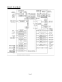
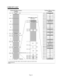
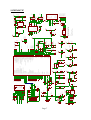
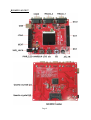
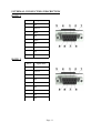
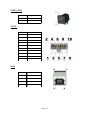
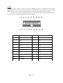
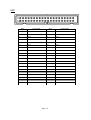
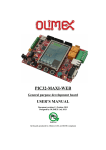
STR750-STK development board
Users Manual
All boards produced by Olimex are ROHS compliant
Revision A, December 2009
Copyright(c) 2010, OLIMEX Ltd, All rights reserved
Page 1
INTRODUCTION
STR750-STK is development board with high performance STR750F
ARM7TDMI-STM microcontroller from STMicroelectronics. This microcontroller
supports serial interfaces such as USB Device, UART, CAN and other. On the board
are available JTAG, TFT LCD and SD/MMC card connector, UEXT, EXT, USB,
CAN and two RS232 connectors. All this allows you to build a diversity of powerful
applications to be used in a wide range of applications.
BOARD FEATURES
•
MCU: STR750
•
Standard JTAG connector with ARM 2x10 pin layout for
programming/debugging with ARM-JTAG
•
USB 2.0 device port
•
2x RS232 interface and drivers
•
3x User Buttons
•
Trimmer potentiometer
•
NOKIA 6610 TFT COLOR LCD display 128x128 pixel 12 bit color with
backlight
•
UEXT - 10 pin extension connector for Olimex addon peripherials like
MP3, RF2.4Ghz, RFID etc. modules
•
On board voltage regulators with up to 800mA current
•
single power supply: 6-9VDC required
•
power supply LED
•
power supply filtering capacitor
•
RESET circuit
•
RESET button
•
4 Mhz crystal
•
PCB: FR-4, 1.5 mm (0,062"), soldermask, silkscreen component print
•
Dimensions: 110.5 x 101.6 mm (4.35 x 3.99")
Page 2
ELECTROSTATIC WARNING
The STR750-STK board is shipped in protective anti-static packaging. The board
must not be subject to high electrostatic potentials. General practice for working
with static sensitive devices should be applied when working with this board.
BOARD USE REQUIREMENTS
Cables: The cable you will need depends on the programmer/debugger you use. If
you use ARM-JTAG-EW, you will need USB A-B cable.
Hardware:
Programmer/Debugger ARM-JTAG-EW or other compatible
programming/debugging tool if you work with EW-ARM.
You can use also ARM-USB-OCD, ARM-USB-TINY, ARM-USB-OCD-H, ARMUSB-TINY-H, but we don't offer a project for this board with this programmers.
PROCESSOR FEATURES
STR750-STK board use STR750F ARM7TDMI-STM microcontroller with on-chip
high-speed single voltage FLASH memory and high-speed RAM from
STMicroelectronics with these features:
−
−
−
Core:
−
ARM7TDMI-S 32-bit RISC CPU
−
56 DMIPS @ 60 MHz
Memories
−
256 Kbytes embedded Flash program memory (10k cycles endurance, data
retention 20 yrs at 55°C)
−
16 Kbytes Read While Write Flash for data storage (100k cycles endurance,
data retention 20 yrs at 55°C)
−
Flash Data Readout Protection
−
16 KBytes embedded SRAM
−
Memory mapped interface to ext. Serial Flash or EEPROM (64 MB) w.boot
capability
Clock, Reset and Supply Management
−
Single supply 3.3V ±10% or 5V ±10%
−
Embedded 1.8V Voltage Regulators with Low Power features
−
Smart Clock Controller with flexible clock generation capability:
−
Internal RC for fast start-up and backup clock mechanism.
−
Up to 60 MHz operation using internal PLL with 4 or 8 MHz
crystal/ceramic osc.
Page 3
−
−
−
−
−
−
Smart Low Power Modes: SLOW, WFI, STOP and STANDBY with backup
registers.
−
Real Time Clock, driven by low power internal RC or 32.768 kHz dedicated
osc, for clock-calendar and Auto Wake-up
Nested interrupt controller
−
Fast interrupt handling with 32 vectors
−
16 IRQ priorities, 2 maskable FIQ sources
−
16 external interrupt / wake-up Lines
DMA
−
4-channel DMA controller
−
Circular buffer management
−
Support for UART, SSP, Timers, ADC
6 Timers
−
16-bit watchdog timer (WDG)
−
16-bit timer for system timebase functions
−
3 Synchronizable timers each with 2 input captures and 2 output
compare/PWMs.
−
16-bit 6-channel synchronizable PWM timer
−
Dead time generation, edge/center-aligned waveforms and emergency
stop
8 Communications Interfaces
−
1 I2C interface
−
3 HiSpeed UARTs w. Modem/LIN capability
−
2 SSP serial interfaces (SPI or SSI)
−
1 CAN interface (2.0B Active)
−
1 USB 2.0, full-speed 12 MB/s interface with 8 configurable endpoint sizes.
10-bit A/D Converter
−
16/11 channels with Fast Scan Mode
−
Programmable Analog Threshold Detection
−
Conversion time: min. 3µs
−
Conversion Range: 0 to VDD_IO
−
72 GPIO lines with High Sink capabilities
−
Development Tools Support
−
JTAG interface (ARM Embedded ICE)
Page 4
BLOCK DIAGRAM
Page 5
MEMORY MAP
Page 6
USB
Page 7
1
2
3
4
CAN_RX
CAN_TX
47uF/6.3VDC
TXD
VSS
VDD
RXD
470uF/16V
C70
100nF
C37
IN
OUT
AGND
C36
0
100nF(NA)
R43
R2
220/1%(NA)
R4
100/1%(NA)
ADJ/GND
47uF/6.3V
SN65HVD230
RS
CANH
CANL
VREF
3.3V
+
R5
120
8
7
6
5
U1
10K
2
R6
220uF/16V/mini
CAN0
5
4
3
2
1
VR2(1.8V)
LM1117(NA)
C31
+
R40
10K
9
8
7
6
3
C35
100nF
R41
10K
1
+
P2.01
R7
390/1%
R20
240/1%
C6
3.3V
OUT
47uF/6.3V(NA)
C5
1.8V
R14
560
PWR
3.3V
STR750F
R32
GND
100nF
C17
330
R13
B1
3.3V
RST
RESET 1
R37
10K
2 VCC
U2 4.7K
MCP130
3.3V
3
CNTRL/HS
GND
IN
ADJ/GND
4MHz
XT2
XT1
R60
0
B1
/RESET
NA
100nF
R38
10K
10
48
74
98
53
97
73
49
54
TXD0/BOOT1
330
R39
B2
3.3V
C22
C29
VSS_IO1
VSS_IO2
VSS_IO3
VSS_IO4
VSS18
VSS18_1
VSSA_ADC
VSSA_PLL
VSSBKP
V18BKP
VDDA_PLL
VDDA_ADC
VREG_DIS
B2
10K
R58
R34
10K
3.3V
33nF
C39
100n
3.3V
AGND
C9
C3 100n
C11 100n
1
R35
10K
100nF
C38
10nF
C1
10uF/6.3V
C43 FB2
330
R33
560
C33
100nF(NA)
1BOOT0
2
3
STAT
3.3V
STAT
WAKEUP
10K
R57
3.3V
10uF/6.3V
C8 FB1
3.3V
EXT-1
EXT-2
EXT-3
EXT-4
1uF/6.3V
C2
ferrite_bead/0805
VDDA
10nF
C42
WAKEUP
R61
2
ferrite_bead/0805
1
AGND
3.3V
R46
4.7K
3.3V
1.8B_E
1.8V
AGND AGND
1BOOT1
BOOT0
2
3
3.3V
2
1.8V_E
EXT-35
EXT-34
EXT-33
EXT-32
EXT-31
EXT-30
EXT-36
VRE
1
100nF
R3
1M
VR1(3.3V)
LM1117
C28
22p
Q1
46
47
USB_DP
USB_DN
XRTC1
XRTC2
NRSTIN
NRSTOUT
TEST
55
45
70
75
96
52
44
69
99
2
5VAC
6VDC
C30
15p(NA)
C14
22p
66
65
57
56
59
58
9
V18
V18REG
VDD_IO1
VDD_IO2
VDD_IO3
ADC_IN6
RXD2
TXD2
+
C34
15p(NA)
C73
USB_DUSB_D+
G ND
/RESET
CS_MMC
STAT
C10
27p
Q2
C32
Q_GNDTC38H_SMD_GND
27p
EXT-29
LCD_BL
LCD_RESET
CS_LCD
P2.00
P2.01
P2.02
P2.03/UART1_RTS
P2.04/TIM2_OC1
P2.05/PWM3N
P2.06/PWM3
P2.07/PWM2N
P2.08/PWM2
P2.09/PWM1N
P2.10
P2.11
P2.12
P2.13
P2.14
P2.15
P2.16
P2.17/UART2_RTS
P2.18
P2.19
R45
4.7K
3.3V
+
C72
R47
R48
R11
10K
R-T
24
23
14
13
12
86
85
84
83
82
72
71
62
61
51
50
43
33
32
31
10uF/6.3V
C40
G1
DB104(SMD)
D2
1N5819S
22
22
TDO
TRST
TDI
TMS
TCK
P2.01
EXT-37
EXT-40
EXT-39
EXT-38
7
3
8
4
Q
D
C
#S
2
5
6
1
AGND
M25P64-VME(NA)
#HOLD
#W/VPP
VCC
VSS
U3
C41
100n
GND15
R1IN
R2IN
http://www.olimex.com/dev
COPYRIGHT(C), 2009
Rev. A
3
MISO0
MOSI0
SCLK0
SPI0_NSS
AN_TR
10K
VDDA
V-
V+
T1OUT
T2OUT
U5PWR
16VCC
R1OUT
R2OUT
T1IN
T2IN
C2-
C2+
C1-
C1+
U5
ST3232
C7
470p
+
STR750-STK
3.3V
330
R56
100nF
C4
AGND
ADC_IN6
3.3V
12
9
RXD2
RXD1
5
4
3
1
11
10
C26
100n
C27
100n
LCD_BL
R28
1K
C15
10u/6.3V
FET1
IRLML6402
TXD2
TXD1
R27
1M
3.3V
L1
220u
FB
SC
SE
6
1
1
2
3
4
5
R59
10K
NC
NC
R24
6
7
8
9
BL_PWR
6
7
8
9
LEDGND
GND
VLED
RESET
SCK
DIO
CS
R25
NC
R23
NC
UEXT-1
UEXT-2
UEXT-3
UEXT-4
UEXT-5
UEXT-6
UEXT-7
UEXT-8
UEXT-9
UEXT-10
VDISPLAY
VDIGITAL
TXD0/BOOT1
RXD0
SCL
SDA
MISO1
MOSI1
SCLK1
SPI1_NSS
3.3V
9
8
10
BL_PWR
2
R26
10K
1
2
3
4
5
R22
R31
1.2k/1%
RS232_1
LCD_RESET
3.3V 3.3V
R30
5.6k/1%
RS232_2
4
3
5
3.3V
D1
1N5819S
SCLK1
MOSI1
CS_LCD
C13
100n
C25
100n
5
1
2
150
R29
MC34063
R36
100K
13
8
14
7
6
2
TC
U6
1
R1
4
USB
+5V_USB
R55
150
EXT-17
EXT-18
EXT-19
EXT-20
EXT-21
EXT-22
EXT-23
EXT-24
EXT-25
EXT-26
EXT-27
EXT-28
EXT-16
RTCK
CAN_RX
CAN_TX
SCLK1
MISO1
MOSI1
SPI1_NSS
RXD1
TXD1
SPI0_NSS
SCLK0
MISO0
MOSI0
SCL
SDA
RXD0
TXD0/BOOT1
BOOT0
+
100n
R49
1.5K
3.3V
R50
10K
R10
NA
4
3
2
100
79
78
77
76
30
29
28
27
26
25
64
63
42
41
40
39
17
16
15
11
38
37
36
35
8
7
6
5
+
C74
R42
10K
/RESET
RTCK
R9
10K
2
1
R12
10K
1
3
5
7
9
11
13
15
17
19
R18 R8
10K 10K
SD/MMC-bot
CP1
CP2
P0.00/TIM0_OC/BOOT0
P0.01/TIM0_TI1/MCO
P0.02/TIM2_OC1/ADC_IN0/EIT0
P0.03/TIM2_TI1/ADC_IN1
P0.04/SMI_CS0/SPI0_NSS
P0.05/SPI0_SCLK/SMI_CK/EIT1
P0.06/SMI_DIN/SPI0_MISO
P0.07/SMI_DOUT/SPI0_MOSI/EIT2
P0.08/I2C_SCL/EIT3
P0.09/I2C_SDA
P0.10/UART0_RX/SMI_CS3/EIT4
P0.11/UART0_TX/BOOT1/SMI_CS2
P0.12/UART0_CTS/ADC_IN2/SMI_CS1
P0.13/RTCK/UART0_RTS
P0.14/CAN_RX/EIT5
P0.15/CAN_TX
P0.16/SPI1_SCLK
P0.17/SPI1_MISO/ADC_IN3
P0.18/SPI1_MOSI
P0.19/USB_CK/SPI1_NSS/ADC_IN4/EIT6
P0.20/UART1_RX
P0.21/UART1_TX
P0.22/UART1_CTS/ADC_IN5
P0.23/UART1_RTS/ADC_IN6
P0.24/UART2_RX
P0.25/UART2_TX
P0.26/UART2_CTS
P0.27/UART2_RTS/ADC_IN7
P0.28/TIM1_OC1
P0.29/TIM1_TI1/ADC_IN8
P0.30/TIM1_OC2
P0.31/TIM1_TI2
VDDA
1
2
3
4
2
4
6
8
10
12
14
16
18
20
JTAG
2K
13
15
U4
P1.00/TIM0_OC2
P1.01/TIM0_TI2
P1.02/TIM2_OC2
P1.03/TIM2_TI2
P1.04/PWM3N/ADC_IN9
P1.05/PWM3/EIT7
P1.06/PWM2N/ADC_IN10
P1.07/PWM2/EIT8
P1.08/PWM1N/ADC_IN11
P1.09/PWM1/EIT9
P1.10/PWM_EMERGENCY/EIT10
P1.11/ADC_IN12/EIT11
P1.12/ADC_IN13/EIT12
P1.13/ADC_IN14/EIT13
P1.14
P1.15/WKP_STDBY/EIT15
P1.16/JTDI
P1.17/JTDO
P1.18/JTCK
P1.19/JTMS
NJTSRST
220uF/16V
C16 +
PWR_JACK
3.3V
R15
CP
B1
B2
CP
WP
WAKEUP
TDI
TDO
TCK
TMS
TRST
95
94
68
67
91
90
89
88
87
81
80
34
1
93
92
60
21
20
19
18
22
VSS
33K
R21
CD/DAT3/CS
CMD/DI
VSS1
VDD
CLK/SCLK
VSS2
DAT0/DO
DAT1/RES
DAT2/RES
WP1
WP2
EXT-5
EXT-6
EXT-7
EXT-8
EXT-9
EXT-10
EXT-11
EXT-12
EXT-13
EXT-14
EXT-15
VCC
3.3V
R52
10
14
SD/MMC
6
3.3V
3.3V
3.3V
MOSI0
WP
1
2
3
4
3.3V
SCLK0
5
10k
6
MISO0
7
10K 8
R53
10K 9
R54
0
100K
2k
33k
DC
IS
MISO0
R17
R19
R16
R51
8
7
SCLK0
CS_MMC
MOSI0
3.3V
3.3V
SCHEMATIC
+
CAN0_T
1
2
BOARD LAYOUT
Page 8
POWER SUPPLY CIRCUIT
STR750-STK can take power (+6 V) from PWR_JACK, and (+5 V) from USB.
The programmed board power consumption is about 140 mA with all peripherials
enabled.
RESET CIRCUIT
STR750-STK reset circuit includes jumper R-T, pin 15 of JTAG connector,
STR750F pin 59 (NRSTIN), U2 (MCP130) and RESET button.
CLOCK CIRCUIT
Quartz crystal 4 MHz is connected to STR750F pin 46 (XT2) and pin 47
(XT1).
Quartz crystal 32.768 kHz is connected to STR750F pin 56 (XRTC2) and pin
57 (XRTC1).
JUMPER DESCRIPTION
CAN0_T
This jumper assures correct work of the CAN. At each end of the bus it should be
closed. This means that if you have only two devices with CAN, the jumpers of both
devices should be closed. If you have more than two devices, only the two enddevices should be closed.
Default state is closed.
1.8V_E
Default state is closed.
1.8B_E
Default state is open.
VRE
Default state is closed.
CNTRL/HS
Default state is in position CNTRL.
R-T
Default state is closed.
BOOT0
Default state is 0.
BOOT1
Default state is 0.
Page 9
INPUT/OUTPUT
Status led (red) with name STAT connected to STR750F pin 31 (P2.19).
Power-on LED (red) with name PWR – this LED shows that +3.3V is applied to the
board.
User button with name B1 connected to STR750F pin 34 (P1.11).
User button with name B2 connected to STR750F pin 1 (P1.12).
User button with name WAKEUP connected to STR750F pin 60
(P1.15/WKP_STDBY).
User button with name RESET connected to STR750F pin 59 (NRSTIN).
Trimpot with name AN_TR connected to STR750F pin 11 (P0.23/ADC_IN6).
TFT LCD - 128x128 12 bit color with backlight.
Page 10
EXTERNAL CONNECTORS DESCRIPTION
RS232_1
Pin #
Signal Name
1
NC
2
T2OUT
3
R2IN
4
NC
5
GND
6
NC
7
NC
8
NC
9
NC
RS232_2
Pin #
Signal Name
1
NC
2
T1OUT
3
R1IN
4
NC
5
GND
6
NC
7
NC
8
NC
9
NC
Page 11
PWR_JACK
Pin #
Signal Name
1
Power Input
2
GND
UEXT
Pin #
Signal Name
1
3.3V
2
GND
3
TXD0/BOOT1
4
RXD0
5
SCL
6
SDA
7
MISO1
8
MOSI1
9
SCLK1
10
SPI1_NSS
USB
Pin #
Signal Name
1
+5V_USB
2
USB_D-
3
USB_D+
4
GND
Page 12
JTAG
The JTAG connector allows the software debugger to talk via a JTAG (Joint Test Action
Group) port directly to the core. Instructions may be inserted and executed by the core thus allowing
STR750 memory to be programmed with code and executed step by step by the host software.
For more details refer to IEEE Standard 1149.1 - 1990 Standard Test Access Port and Boundary
Scan Architecture and STR750 datasheets and users manual.
Pin #
Signal Name
Pin #
Signal Name
1
3.3V
2
3.3V
3
TRST
4
GND
5
TDI
6
GND
7
TMS
8
GND
9
TCK
10
GND
11
RTCK
12
GND
13
TDO
14
GND
15
/RESET
16
GND
17
pull-down
18
GND
19
+5V_J-LINK
20
GND
Page 13
EXT
Pin #
Signal Name
Pin #
Signal Name
1
3.3V
2
GND
3
AVDD
4
AGND
5
P1.00
6
P1.01
7
P1.02
8
P1.03
9
P1.04
10
P1.05
11
P1.06
12
P1.07
13
P1.08
14
P1.09
15
P1.10
16
P2.00
17
P2.02
18
P2.03
19
P2.04
20
P2.05
21
P2.06
22
P2.07
23
P2.08
24
P2.09
25
P2.10
26
P2.11
27
P2.12
28
P2.13
29
P2.17
30
P0.31
31
P0.30
32
P0.29
33
P0.28
34
P0.27
35
P0.26
36
P0.22
37
P0.12
38
P0.03
39
P0.02
40
P0.01
Page 14
SD/MMC
Pin #
Signal Name
Pin #
Signal Name
1
CS_MMC
2
MOSI0
3
GND
4
VDD
5
SCLK0
6
GND
7
MISO0
8
pull-up
9
pull-up
10
WP
11
-
12
-
13
CP
14
pull-down
15
pull-down
CAN0
Pin #
Signal Name
1
NC
2
JMP CAN0_T; CANL
3
GND
4
NC
5
NC
6
GND
7
CANH
8
pull-down
9
pull-up
Page 15
MECHANICAL DIMENSIONS
Page 16
AVAILABLE DEMO SOFTWARE
–
Jim Lynch's NOKIA 6610 LCD tutorial
–
OpenOCD + Eclipse set of projects 1.00 include flash write make file for
STR-750STK.
Page 17
ORDER CODE
STR750-STK - assembled and tested board, includes STR750
microcontroller
How to order?
You can order to us directly or by any of our distributors.
Check our web www.olimex.com/dev for more info.
Revision history
Revision A, December 2009
Page 18
Disclaimer
© 2010 Olimex Ltd. All rights reserved. Olimex®, logo and combinations thereof, are registered
trademarks of Olimex Ltd. Other terms and product names may be trademarks of others.
The information in this document is provided in connection with Olimex products. No license, express
or implied or otherwise, to any intellectual property right is granted by this document or in
connection with the sale of Olimex products.
Neither the whole nor any part of the information contained in or the product described in this
document may be adapted or reproduced in any material from except with the prior written
permission of the copyright holder.
The product described in this document is subject to continuous development and improvements. All
particulars of the product and its use contained in this document are given by OLIMEX in good faith.
However all warranties implied or expressed including but not limited to implied warranties of
merchantability or fitness for purpose are excluded.
This document is intended only to assist the reader in the use of the product. OLIMEX Ltd. shall not
be liable for any loss or damage arising from the use of any information in this document or any error
or omission in such information or any incorrect use of the product.
Page 19