1
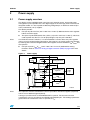
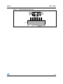
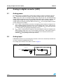
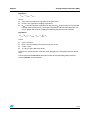
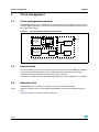
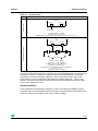
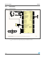
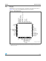
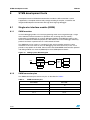
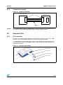
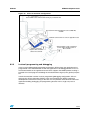
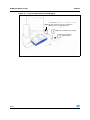
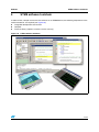
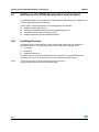
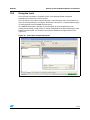
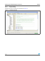
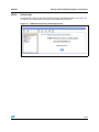
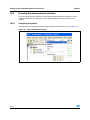
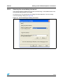
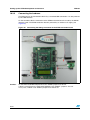
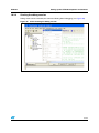
AN2752
Application note
Getting started with the STM8S
Introduction
This application note complements the information in the STM8S datasheets by describing
the minimum hardware and software environment required to build an application around an
STM8S 8-bit microcontroller device. It is divided into the following sections:
■
Power supply
■
Analog-to-digital converter (ADC)
■
Clock management
■
Reset control and development
■
Debugging tool support
■
STM8 software toolchain
■
Setting up the STM8 development environment
This application note also contains detailed reference design schematics with descriptions
of the main components. In addition, some hardware recommendations are given.
September 2008
Rev 2
1/42
www.st.com
Contents
AN2752
Contents
1
Hardware requirements summary . . . . . . . . . . . . . . . . . . . . . . . . . . . . . . 6
2
Power supply . . . . . . . . . . . . . . . . . . . . . . . . . . . . . . . . . . . . . . . . . . . . . . . 7
3
4
5
2.1
Power supply overview . . . . . . . . . . . . . . . . . . . . . . . . . . . . . . . . . . . . . . . . 7
2.2
Main operating voltages . . . . . . . . . . . . . . . . . . . . . . . . . . . . . . . . . . . . . . . 8
2.3
Power-on/power-down reset (POR/PDR) . . . . . . . . . . . . . . . . . . . . . . . . . . 8
Analog-to-digital converter (ADC) . . . . . . . . . . . . . . . . . . . . . . . . . . . . . 10
3.1
Analog power . . . . . . . . . . . . . . . . . . . . . . . . . . . . . . . . . . . . . . . . . . . . . . 10
3.2
Analog input . . . . . . . . . . . . . . . . . . . . . . . . . . . . . . . . . . . . . . . . . . . . . . . 10
Clock management . . . . . . . . . . . . . . . . . . . . . . . . . . . . . . . . . . . . . . . . . 12
4.1
Clock management overview . . . . . . . . . . . . . . . . . . . . . . . . . . . . . . . . . . 12
4.2
Internal clock . . . . . . . . . . . . . . . . . . . . . . . . . . . . . . . . . . . . . . . . . . . . . . 12
4.3
External clock . . . . . . . . . . . . . . . . . . . . . . . . . . . . . . . . . . . . . . . . . . . . . . 12
Reset control . . . . . . . . . . . . . . . . . . . . . . . . . . . . . . . . . . . . . . . . . . . . . . 14
5.1
Reset management overview . . . . . . . . . . . . . . . . . . . . . . . . . . . . . . . . . . 14
5.2
Hardware reset implantation . . . . . . . . . . . . . . . . . . . . . . . . . . . . . . . . . . 15
5.2.1
6
7
2/42
RC circuit . . . . . . . . . . . . . . . . . . . . . . . . . . . . . . . . . . . . . . . . . . . . . . . . 16
Recommendations . . . . . . . . . . . . . . . . . . . . . . . . . . . . . . . . . . . . . . . . . 17
6.1
Printed circuit board . . . . . . . . . . . . . . . . . . . . . . . . . . . . . . . . . . . . . . . . . 17
6.2
Component position . . . . . . . . . . . . . . . . . . . . . . . . . . . . . . . . . . . . . . . . . 17
6.3
Ground and power supply (VSS, VDD) . . . . . . . . . . . . . . . . . . . . . . . . . . . 17
6.4
Decoupling . . . . . . . . . . . . . . . . . . . . . . . . . . . . . . . . . . . . . . . . . . . . . . . . 17
6.5
Other signals . . . . . . . . . . . . . . . . . . . . . . . . . . . . . . . . . . . . . . . . . . . . . . 18
6.6
Unused I/Os and features . . . . . . . . . . . . . . . . . . . . . . . . . . . . . . . . . . . . 18
6.7
User options . . . . . . . . . . . . . . . . . . . . . . . . . . . . . . . . . . . . . . . . . . . . . . . 18
Reference design . . . . . . . . . . . . . . . . . . . . . . . . . . . . . . . . . . . . . . . . . . 19
7.1
Components reference . . . . . . . . . . . . . . . . . . . . . . . . . . . . . . . . . . . . . . . 19
7.2
Schematics . . . . . . . . . . . . . . . . . . . . . . . . . . . . . . . . . . . . . . . . . . . . . . . . 20
AN2752
Contents
7.3
8
STM8 development tools . . . . . . . . . . . . . . . . . . . . . . . . . . . . . . . . . . . . 22
8.1
8.2
9
10
Pinouts . . . . . . . . . . . . . . . . . . . . . . . . . . . . . . . . . . . . . . . . . . . . . . . . . . . 21
Single wire interface module (SWIM) . . . . . . . . . . . . . . . . . . . . . . . . . . . . 22
8.1.1
SWIM overview . . . . . . . . . . . . . . . . . . . . . . . . . . . . . . . . . . . . . . . . . . . 22
8.1.2
SWIM connector pins . . . . . . . . . . . . . . . . . . . . . . . . . . . . . . . . . . . . . . . 22
8.1.3
Hardware connection . . . . . . . . . . . . . . . . . . . . . . . . . . . . . . . . . . . . . . . 23
Emulator STice . . . . . . . . . . . . . . . . . . . . . . . . . . . . . . . . . . . . . . . . . . . . . 23
8.2.1
STice overview . . . . . . . . . . . . . . . . . . . . . . . . . . . . . . . . . . . . . . . . . . . . 23
8.2.2
STice in emulation configuration . . . . . . . . . . . . . . . . . . . . . . . . . . . . . . 24
8.2.3
In-circuit programming and debugging . . . . . . . . . . . . . . . . . . . . . . . . . 25
STM8 software toolchain . . . . . . . . . . . . . . . . . . . . . . . . . . . . . . . . . . . . 27
9.1
Integrated development environment . . . . . . . . . . . . . . . . . . . . . . . . . . . . 28
9.2
Compiler . . . . . . . . . . . . . . . . . . . . . . . . . . . . . . . . . . . . . . . . . . . . . . . . . . 28
9.3
Firmware library . . . . . . . . . . . . . . . . . . . . . . . . . . . . . . . . . . . . . . . . . . . . 29
Setting up the STM8 development environment . . . . . . . . . . . . . . . . . 30
10.1
Installing the tools . . . . . . . . . . . . . . . . . . . . . . . . . . . . . . . . . . . . . . . . . . . 30
10.2
Using the tools . . . . . . . . . . . . . . . . . . . . . . . . . . . . . . . . . . . . . . . . . . . . . 31
10.3
10.2.1
Project editing . . . . . . . . . . . . . . . . . . . . . . . . . . . . . . . . . . . . . . . . . . . . 32
10.2.2
Online help . . . . . . . . . . . . . . . . . . . . . . . . . . . . . . . . . . . . . . . . . . . . . . . 33
Running the demonstration software . . . . . . . . . . . . . . . . . . . . . . . . . . . . 34
10.3.1
Compiling the project . . . . . . . . . . . . . . . . . . . . . . . . . . . . . . . . . . . . . . . 34
10.3.2
Selecting the correct debug instrument . . . . . . . . . . . . . . . . . . . . . . . . . 35
10.3.3
Connecting the hardware . . . . . . . . . . . . . . . . . . . . . . . . . . . . . . . . . . . . 36
10.3.4
Starting the debug session . . . . . . . . . . . . . . . . . . . . . . . . . . . . . . . . . . 37
10.3.5
Running the software . . . . . . . . . . . . . . . . . . . . . . . . . . . . . . . . . . . . . . . 38
10.3.6
Follow up . . . . . . . . . . . . . . . . . . . . . . . . . . . . . . . . . . . . . . . . . . . . . . . . 39
11
Documentation and online support . . . . . . . . . . . . . . . . . . . . . . . . . . . . 40
12
Revision history . . . . . . . . . . . . . . . . . . . . . . . . . . . . . . . . . . . . . . . . . . . 41
3/42
List of tables
AN2752
List of tables
Table 1.
Table 2.
Table 3.
4/42
Component list . . . . . . . . . . . . . . . . . . . . . . . . . . . . . . . . . . . . . . . . . . . . . . . . . . . . . . . . . . 19
SWIM connector pins . . . . . . . . . . . . . . . . . . . . . . . . . . . . . . . . . . . . . . . . . . . . . . . . . . . . . 22
Document revision history . . . . . . . . . . . . . . . . . . . . . . . . . . . . . . . . . . . . . . . . . . . . . . . . . 41
AN2752
List of figures
List of figures
Figure 1.
Figure 2.
Figure 3.
Figure 4.
Figure 5.
Figure 6.
Figure 7.
Figure 8.
Figure 9.
Figure 10.
Figure 11.
Figure 12.
Figure 13.
Figure 14.
Figure 15.
Figure 16.
Figure 17.
Figure 18.
Figure 19.
Figure 20.
Figure 21.
Figure 22.
Figure 23.
Figure 24.
Figure 25.
Figure 26.
Figure 27.
Figure 28.
Power supply . . . . . . . . . . . . . . . . . . . . . . . . . . . . . . . . . . . . . . . . . . . . . . . . . . . . . . . . . . . . 7
External capacitor . . . . . . . . . . . . . . . . . . . . . . . . . . . . . . . . . . . . . . . . . . . . . . . . . . . . . . . . . 8
Typical layout of VDD/VSS pair . . . . . . . . . . . . . . . . . . . . . . . . . . . . . . . . . . . . . . . . . . . . . . . 9
Analog input interface . . . . . . . . . . . . . . . . . . . . . . . . . . . . . . . . . . . . . . . . . . . . . . . . . . . . . 10
System clock distribution internal clock . . . . . . . . . . . . . . . . . . . . . . . . . . . . . . . . . . . . . . . 12
Clock sources . . . . . . . . . . . . . . . . . . . . . . . . . . . . . . . . . . . . . . . . . . . . . . . . . . . . . . . . . . 13
Reset management . . . . . . . . . . . . . . . . . . . . . . . . . . . . . . . . . . . . . . . . . . . . . . . . . . . . . . 14
Output characteristics . . . . . . . . . . . . . . . . . . . . . . . . . . . . . . . . . . . . . . . . . . . . . . . . . . . . . 15
Input characteristics . . . . . . . . . . . . . . . . . . . . . . . . . . . . . . . . . . . . . . . . . . . . . . . . . . . . . . 15
RC circuit . . . . . . . . . . . . . . . . . . . . . . . . . . . . . . . . . . . . . . . . . . . . . . . . . . . . . . . . . . . . . . 16
Reference design . . . . . . . . . . . . . . . . . . . . . . . . . . . . . . . . . . . . . . . . . . . . . . . . . . . . . . . . 20
LQFP 80-pin pinout. . . . . . . . . . . . . . . . . . . . . . . . . . . . . . . . . . . . . . . . . . . . . . . . . . . . . . . 21
Debug system block diagram . . . . . . . . . . . . . . . . . . . . . . . . . . . . . . . . . . . . . . . . . . . . . . . 22
Hardware connection . . . . . . . . . . . . . . . . . . . . . . . . . . . . . . . . . . . . . . . . . . . . . . . . . . . . . 23
Connection description . . . . . . . . . . . . . . . . . . . . . . . . . . . . . . . . . . . . . . . . . . . . . . . . . . . . 23
STice in emulation configuration . . . . . . . . . . . . . . . . . . . . . . . . . . . . . . . . . . . . . . . . . . . . 25
In-circuit programming and debugging . . . . . . . . . . . . . . . . . . . . . . . . . . . . . . . . . . . . . . . . 26
STM8 software toolchain . . . . . . . . . . . . . . . . . . . . . . . . . . . . . . . . . . . . . . . . . . . . . . . . . . 27
STM8 firmware library examples . . . . . . . . . . . . . . . . . . . . . . . . . . . . . . . . . . . . . . . . . . . . 29
STVD open example workspace . . . . . . . . . . . . . . . . . . . . . . . . . . . . . . . . . . . . . . . . . . . . 31
STVD MCU edit mode . . . . . . . . . . . . . . . . . . . . . . . . . . . . . . . . . . . . . . . . . . . . . . . . . . . . 32
STM8 firmware library online help manual . . . . . . . . . . . . . . . . . . . . . . . . . . . . . . . . . . . . . 33
STVD: Building the project . . . . . . . . . . . . . . . . . . . . . . . . . . . . . . . . . . . . . . . . . . . . . . . . . 34
STVD: Selecting the debug instrument. . . . . . . . . . . . . . . . . . . . . . . . . . . . . . . . . . . . . . . . 35
Connecting the debug instrument to the STM8 evaluation board. . . . . . . . . . . . . . . . . . . . 36
STVD: Starting the debug session . . . . . . . . . . . . . . . . . . . . . . . . . . . . . . . . . . . . . . . . . . . 37
STVD: Run the software . . . . . . . . . . . . . . . . . . . . . . . . . . . . . . . . . . . . . . . . . . . . . . . . . . . 38
STM8 evaluation board. . . . . . . . . . . . . . . . . . . . . . . . . . . . . . . . . . . . . . . . . . . . . . . . . . . . 39
5/42
Hardware requirements summary
1
AN2752
Hardware requirements summary
In order to build an application around an STM8S device, the application board should, at
least, provide the following features:
6/42
●
Power supply
●
Clock management
●
Reset management
●
Debugging tool support: Single wire interface module (SWIM) connector
AN2752
Power supply
2
Power supply
2.1
Power supply overview
The device can be supplied through a 3.0 V to 5.5 V external source. An on-chip power
management system provides the 1.8 V digital supply to the core logic, both in normal and
low power modes. It is also capable of detecting voltage drops, on both main external (3.3
V/5 V) and internal (1.8 V) supplies.
The device provides:
●
One pair of pads VDD/VSS (3.3 V ± 0.3 V to 5 V ± 0.5 V) dedicated to the main regulator
ballast transistor supply.
●
Note:
Two pairs of pads dedicated for VDD_IO/VSS_IO (3.3 V ± 0.3 V to 5 V ± 0.5 V), which are
used to power only the I/O’s. On 32-pin packages, only one pair is bonded.
For VDDIO/VSSIO next to VDD/VSS, it is recommended to connect these two pairs together
and to use only one decoupling capacitance. The purpose is to ensure good noise immunity
by reducing the connection length between both supplies and also between VDD/VDDIO and
the capacitor.
●
One pair of pads VDDA/VSSA (3.3 V ± 0.3 V to 5 V ± 0.5 V) dedicated to analog
functions. Refer to Section 3: Analog-to-digital converter (ADC) on page 10 for more
details.
Figure 1.
Power supply
Analog
signal
VDDA
VSSA
Analog functions
VCAP
3.3V - 5V
VDD/VDDIO1
VSS/VSSIO1
CPU
RAM
Logic
VDDIO2
VSSIO2
OSCIN
Star connected
Note:
Main / Low power
regulator
OSCOUT
VDDIO
VDDIO
IOs
VSSIO
VSSIO
XTAL
ai15330
The capacitors must be connected as close as possible to the device supplies (especially
VDD in case of dedicated ground plane).
Placing a crystal/resonator on OSCIN/OSCOUT is optional. The resonator must be
connected as close as possible to the OSCIN and OSCOUT pins. The loading capacitance
ground must be connected as close as possible to VSS.
7/42
Power supply
2.2
AN2752
Main operating voltages
STM8S devices are processed in 0.13 µm technology. The STM8S core and I/O peripherals
need different power supplies. In fact, STM8S devices have an internal regulator with a
nominal target output of 1.8 V.
Stabilization for the main regulator is achieved using an external capacitor via the VCAP pin.
The typical value is 470 nF with low equivalent series resistance (ESR). Care should be
taken to limit the series inductance per pad to less than 15 nH.
Figure 2.
External capacitor
ESR
C
ESL
Rleak
Where:
ESR is the equivalent series resistance
ESL is the equivalent inductance
The typical value of C is 470 nF
with an ESR between 0.05...0.2 Ohm
2.3
Power-on/power-down reset (POR/PDR)
The input supply to the main and low power regulators is monitored by a power-on/powerdown reset circuit. The monitoring voltage range is 0.7 V to 2.7 V.
During power-on, the POR/PDR keeps the device under reset until the supply voltages (VDD
and VDDIO) reach their specified working area.
At power-on, a defined reset should be maintained below 0.7 V. The upper threshold for a
reset release is defined in the electrical characteristics section of the product datasheet.
A hysteresis is implemented (POR > PDR) to ensure clean detection of voltage rise and fall.
The POR/PDR also generates a reset when the supply voltage drops below the VPOR/PDR
threshold (isolated and repetitive events).
Recommendations
All pins need to be properly connected to the power supplies. These connections, including
pads, tracks and vias should have the lowest possible impedance. This is typically achieved
with thick track widths and preferably dedicated power supply planes in multi-layer printed
circuit boards (PCBs).
In addition, each power supply pair should be decoupled with filtering ceramic capacitors (C)
at 100 nF with one chemical C (1..2 µF) in parallel on the STM8S device. The ceramic
capacitors should be placed as close as possible to the appropriate pins, or below the
appropriate pins, on the opposite side of the PCB. Typical values are 10 nF to 100 nF, but
exact values depend on the application needs. Figure 3 shows the typical layout of such a
VDD/VSS pair.
8/42
AN2752
Power supply
Figure 3.
Typical layout of VDD/VSS pair
Via to VDD
Via to VSS
Cap.
VDD
VSS
STM8
9/42
Analog-to-digital converter (ADC)
AN2752
3
Analog-to-digital converter (ADC)
3.1
Analog power
The ADC unit has an independent, analog supply reference voltage, isolated on input pin
VDDA, which allows the ADC to accept a very clean voltage source. This analog voltage
supply range is the same as the digital voltage supply range on pin VDD. An isolated analog
supply ground connection on pin VSSA provides further ADC supply isolation. Together, the
analog supply voltage and analog supply ground connection, offer a separate external
analog reference voltage input for the ADC unit on the VREF+ pin. This gives better accuracy
on low voltage input as follows:
3.2
●
VREF+ (input, analog reference positive): The higher/positive reference voltage for the
ADC should be between [250 mV, VDDA]. For more details about VREF+ values please
refer to the STM8S20xxx datasheet. This input is bonded to VDDA in devices that have
no external VREF+ pin (packages with 48 pins or less).
●
VREF- (input, analog reference negative): The lower/negative reference voltage for the
ADC should be higher than VSSA. For more details about VREF- values please refer to
the STM8S20xxx datasheet. This input is bonded to VSSA in devices that have no
external VREF- pin (packages with 48 pins or less).
Analog input
STM8S20xxx devices have 16 analog input channels, which are converted by the ADC one
at a time, and each multiplexed with an I/O.
The analog input interface of the ADC is shown in Figure 4.
Figure 4.
Analog input interface
Outside ADC
VIN
VIN_EXT
REXT
CEXT
10/42
Inside ADC
SWSAMP
CSAMP
AN2752
Analog-to-digital converter (ADC)
Equation 1:
C VIN = C SAMP + C EXT
where:
●
CVIN is the total equivalent capacitor on the path of VIN
●
CSAMP is the equivalent sampling capacitance
●
CEXT is the total external capacitance on the path of VIN to the macro pin. This includes
parasitic routing capacitance, pad and pin capacitance and external capacitance. To
ensure proper and accurate sampling the following equation must be satisfied
Equation 2:
3
( R SW + R EXT ) × ( C SAMP + C EXT ) < ⎛ ------⎞ × T S
⎝ 10⎠
where:
●
RSW = 30 kOhm
●
REXT is the total external resistance on the path of VIN
●
CSAMP = 3 pF
●
TS = 0.5 µs (for 2 MHz input CLK)
Equation 2 is specific for REXT and CEXT when designing an analog input interface for the
ADC.
Please refer to the STM8S20xxx datasheet and/or the corresponding family reference
manual (RM0016) for more details.
11/42
Clock management
AN2752
4
Clock management
4.1
Clock management overview
STM8S20xxx devices offer a flexible way of selecting the core and peripheral clocks (ADC,
memory, digital peripherals). The devices have internal and external clock source inputs and
one output clock (CCO).
Figure 5.
System clock distribution internal clock
OSCIN
1 to 24 MHz
crystal
and external
clock
External clock
16 MHz/128 kHz
internal RC
CCO pin
Clock unit
OSCOUT
Prescaler
lnternal clock
WDG/AWU
Timer
Clock distribution
For more details please refer to the section on clock management in the datasheet
4.2
Internal clock
The RC oscillator has an internal capacitor (C) and an internal resistor ladder (R). STM8S
devices have two kinds of internal clock: a high speed internal clock (HSI) running at
16 MHz and a low speed internal clock (LSI) running at 128 kHz.
After reset, the CPU starts with the internal RC (HSI clock signal) divided by 8, i.e. 2 MHz.
4.3
External clock
STM8S devices can connect to an external crystal or an external oscillator.
Note:
When no external clock is used, OSCIN and OSCOUT can be used as general purpose
I/Os.
Figure 6 describes the external clock connections.
12/42
AN2752
Clock management
Figure 6.
Clock sources
Hardware configuration
STM8
External clock
OSCIN
OSCOUT
(I/O available)
External source
Frequency: 32 kHz … 24 MHz
Comparator hysteresis: 0.1 * VDD
Caution: Without prescaler, a duty cycle of maximum 45/55% must be respected
STM8
Crystal/ceramic resonators
OSCIN
OSCOUT
Q1
CL1
CL2
Load capacitors
Frequency range: 1-24 MHz
Wake-up time: < 2 ms @ 24 MHz
Oscillation mode: Preferred fundamental
Output duty cycle: Max 55/45%
I/O’s: Standard I/O pins multiplexed with OSCIN and OSCOUT
Cload: 10 … 20 pF
Maximum crystal power: 100 µW
The values of the load capacitors CL1 and CL2 are heavily dependent on the crystal type and
frequency. The user can refer to the datasheet of the crystal manufacturer to select the
capacitances. For best oscillation stability CL1 and CL2 normally have the same value.
Typical values are in the range from below 20 pF up to 40 pF (cload: 10 … 20 pF). The
parasitic capacitance of the board layout also needs to be considered and typically adds a
few pF to the component values.
Recommendations
In the PCB layout all connections should be as short as possible. Any additional signals,
especially those that could interfere with the oscillator, should be locally separated from the
PCB area around the oscillation circuit using suitable shielding.
13/42
Reset control
AN2752
5
Reset control
5.1
Reset management overview
The reset cell is a dedicated 5 V bidirectional I/O. Its output buffer driving capability is fixed
to IolMIN = 2 mA @ 0.4 V in the 3 V to 5.5 V range which includes a 40 k pull-up. Output
buffer is reduced to the n-channel MOSFET (NMOS). If a 40 k pull-up is accepted, this cell
does not include an output buffer of 5 V capability. The receiver includes a glitch filter,
whereas the output buffer includes a 20 µs delay.
There are many reset sources, including:
●
External reset through the NRST pin
●
Power-on reset (POR) and brown-out reset (BOR): During power-on, the POR keeps
the device under reset until the supply voltage (VDD and VDDIO) reach the voltage level
at which the BOR starts to function.
●
Independent watchdog reset (IWDG)
●
Window watchdog reset (WWDG)
●
Software reset: The application software can trigger reset
●
SWIM reset: An external device connected to the SWIM interface can request the
SWIM block to generate a microcontroller reset
●
Illegal opcode reset: If a code to be executed does not correspond to any opcode or
prebyte value, a reset is generated
●
Electromagnetic susceptibility (EMS) reset: Generated if critical registers are corrupted
or badly loaded
Figure 7.
Reset management
Simplified functional I/O reset schematic
STM8
VDD_IO
External reset
RPU
Filter
NRST
System reset
Illegal op code reset
Pulse generator
(min 20 µs)
Delay
14/42
IWDG/WWDG/software reset
SWIM reset
EMS reset
POR/BOR reset
AN2752
Reset control
Output characteristics
●
A valid pulse on the pin is guaranteed with a ≥ 20 ns pulse duration on the internal
output buffer.
●
After a valid pulse is recognized, a pulse on the pin of at least 20 µs is guaranteed
starting from the falling edge of A.
Figure 8.
Output characteristics
≥ 20 ns
A
20 µs pulse stretch min.
Pad
Reset requested
Input characteristics
●
All pulses with a duration less than 75 ns are filtered
●
All train/burst spikes with a ratio of 1/10 must be filtered. This means that a negative
spike of up to 75 ns is always filtered, when a 7.5 ns interval between spikes occurs
(ratio 1/10).
●
All pulses with duration more than 450 ns are recognized as valid pulses
●
After a valid pulse is recognized, an internal pulse of at least 30 ns is guaranteed
Figure 9.
Input characteristics
>7.5 ns
>7.5 ns
450 ns
<75 ns
<75 ns
Pad
<75 ns
>30 ns
Negative train of glitch filtered
5.2
Reset requested
System reset
Hardware reset implantation
There are several reset implementation schemes to choose from, such as power supply
behavior, based on the specific parameters of the application. Whatever the solution
chosen, the idea is to keep the RESET pin at a low logic level until the supply has reached a
safe operating voltage. Therefore, the external circuit should be designed in such a manner
that there is enough delay to keep the RESET pin below the VIL value.
15/42
Reset control
5.2.1
AN2752
RC circuit
The RC circuit concept is the simplest and most cost-effective external reset solution, where
the supply waveform is monotonous and the maximum rise time is known. The principle is to
let the RESET pin rise with the microcontroller supply voltage after a delay. The circuit is
shown in Figure 10.
The basic solution is to use an RC delay determined by the rise rate of the supply itself. The
component values must be chosen to create enough delay to keep the RESET pin below the
VIL specification until VCC reaches a safe operating voltage. Normally, a delay (time
constant) corresponding to at least 30 % of the total rise time is advised.
Figure 10. RC circuit
STM8
VDD_IO
RPU
NRSTIN
Push button
C1
100nF
The RC circuit scheme requires a certain delay between a power-down and the next powerup, because the delay generator has to be reinitialized. In practice, a pull-down capacitor
between RESET and VSS needs to be discharged.
16/42
AN2752
Recommendations
6
Recommendations
6.1
Printed circuit board
For technical reasons, it is best to use a multi-layer PCB with a separate layer dedicated to
the VSS and another layer to the VDD supply, which results in a good decoupling, as well as
a good shielding effect. For many applications, economical requirements prohibit the use of
this type of board. In this case, the most important feature is to ensure a good structure for
the VSS and power supply.
6.2
Component position
A preliminary layout of the PCB must separate the different circuits according to their
electromagnetic interference (EMI) contribution in order to reduce cross-coupling on the
PCB, i.e. noisy, high-current circuits, low voltage circuits, and digital components.
6.3
Ground and power supply (VSS, VDD)
The VSS should be distributed individually to every block (noisy, low level sensitive, and
digital) with a single point for gathering all ground returns. Loops must be avoided or have a
minimum surface. The power supply should be implemented close to the ground line to
minimize the surface of the supply loop. This is due to the fact that the supply loop acts as
an antenna, and is therefore the main emitter and receiver of EMI. All component-free
surfaces of the PCB must be filled with additional grounding to create a kind of shield
(especially when using single-layer PCBs).
6.4
Decoupling
The standard decoupler for the external power is a 100 µF pool capacitor. Supplementary
100 nF capacitors must be placed as close as possible to the VSS/VDD pins of the micro in
order to reduce the area of the current loop.
As a general rule, decoupling all sensitive or noisy signals improves electromagnetic compatibility (EMC) performances.
There are 2 types of decouplers:
●
Capacitors close to components. Inductive characteristics, which apply to all capacitors
beyond a certain frequency, must be taken into account. If possible, parallel capacitors
with decreasing values (0.1, 0.01,... µF) should be used.
●
Inductors. Although often ignored, ferrite beads, for example, are excellent inductors
due to their good dissipation of EMI energy and there is no loss of DC voltage (which is
not the case when simple resistors are used).
17/42
Recommendations
6.5
AN2752
Other signals
When designing an application, the following areas should be closely studied to improve
EMC performances:
●
Noisy signals (clock)
●
Sensitive signals (high impedance)
In addition to:
●
Signals for which a temporary disturbance permanently affects operation of the
application, for example, interrupts and handshaking strobe signals (but not LED
commands).
A surrounding VSS trace for such signals increases EMC performances, as does a shorter
length or absence of noisy and sensitive traces (crosstalk effect).
For digital signals, the best possible electrical margin must be reached for the 2 logical
states. Slow Schmitt triggers are recommended for eliminating parasitic states.
6.6
Unused I/Os and features
Microcontrollers are designed for a variety of applications, where often a particular
application does not use 100 % of the microcontroller resources.
To increase EMC performance, unused clocks, counters, or I/Os, should not be left free, for
example, I/Os should be set to ‘0’ or ‘1’ (pull-up or pull-down to the unused I/O pins) and
unused functions should be ‘frozen’ or disabled.
Alternatively, unused I/Os can be programmed as push-pull ‘low’ in order to keep them at a
defined level but not to use external components.
6.7
User options
STM8S devices have user option features that can be used for remapping or
enabling/disabling an automatic reset or low speed watchdog. For more details please refer
to the product datasheet.
18/42
AN2752
Reference design
7
Reference design
7.1
Components reference
Table 1.
ID
Component list
Component name
Reference
Quantity
Comments
Refer to the ‘Pinouts and pin description’
and ‘Package characteristics’ sections of
the STM8S20xxx datasheet, to choose
the right package
1
Microcontroller
STM8S
1
2
Push button
1
1
3
Resistor
10 kOhm
1
4
Capacitor
100 nF
5
Ceramic capacitor (decoupling capacitor)
5
Capacitor
1 µF
1
Decoupling capacitor
6
Capacitor
470 nF
1
Main regulator stabilization
7
Capacitor
20..40 pF
2
Used for crystal
8
Crystal
1..24 MHz
1
9
SWIM connector
4 pins
1
19/42
Reference design
7.2
AN2752
Schematics
B1
C2
20 pF
100 nF
C3
4
1
C1
PA0
PA1
PA2
24M Hz
3
2
Figure 11. Reference design
VCAP
20 pF
Clock(H SE )
R eset
X1
C4
470 nF
4
3
2
1
73
74
75
76
77
78
79
80
SW IM connector
Debug
VDD 2)
VDD 2)
VDD 2)
C6
100 nF
C7
100 nF
C8
100 nF
Decoupling Capacitor
34
33
32
31
30
29
28
27
42
43
44
45
46
47
50
51
CN1
C5
100 nF
1
2
3
9
10
11
12
6
C9
1 µF
8
49
7
23
5
24
4
48
U1
STM8 Package LQF P 80-pin
NRST
PE0/CLK_CCO
PA1/OSCIN
PE1/I 2C_SCL
PA2/OSCOUT
PE2/I 2C_SDA
PA3/TIM2_CH3[TIM3_CH1] PE3/TIM1_BKIN
PA4/UART1_RX
PE4
PA5/UART1_TX
PE5/SP I_NSS
PA6/UART1_CK
PE7/AIN8
VCAP
PE6/AIN9
PB0/AIN0[TIM1_CH1N]
PB1/AIN1[TIM1_CH2N]
PB2/AIN2[TIM1_CH3N]
PB3/AIN3[TIM1_ETR]
PB4/AIN4[I2C_SCL]
PB5/AIN5[I2C_SDA]
PB6/AIN6
PB7/AIN7
PC0/ADC_ ETR
PC1/TIM1_CH1
PC2/TIM1_CH2
PC3/TIM1_CH3
PC4/TIM1_CH4
PC5/SPI_SCK
PC6/SPI_MOSI
PC7/SPI_MI SO
PF0/AI N10
PF1/VREF PF2/VREF +
PF3/AI N11
PF4/AI N12
PF5/AI N13
PF6/AI N14
PF7/AI N15
PG0/CAN_TX
PG1/CAN_RX
PG2
PG3
PG4
PG5
PG6
PG7
PD0/TIM3_CH2[TIM1_BKIN][CLK_CCO] PH0
PD1/SWIM
PH1
PD2/TIM3_CH1[TIM2_CH3]
PH2
PD3/TIM2_CH2[ADC_ETR]
PH3
PD4/TIM2_CH1[BEE P]
PH4/TI M1_ETR
PD5/UART3_TX
PH5/TIM1_CH3N
PD6/UART3_RX
PH6/TIM1_CH2N
PD7/TL I[TIM1_CH4]
PH7/TIM1_CH1N
VDDIO_1
VDDI O_2
VDD
VDDA
VSS
VSSA
VSSIO_1
VSSIO_2
PI0
PI1
PI2
PI3
PI4
PI5
PI6
PI7
26
25 PF1
22 PF2
21
20
19
18
17
R1
R2
0
0
1. If pins 22 or 25 are required as GPIO, R1 and R2 should be removed.
2. VDD must be within the allowed supply voltage range of the STM8S microcontroller.
1)
VDD 2)
52
53
54
55
56
63
64
65
13
14
15
16
35
36
37
38
57
58
59
60
61
62
71
72
MCU
[ ] alternate function remapping option (If the same alternate function is shown twice, it indicates an exclusive choice not a
duplication of the function).
20/42
70
69
68
67
66
41
40
39
ai15471B
AN2752
Pinouts
STM8S devices have several package types, including the LQFP 80-pin pinout shown in
Figure 12. Please refer to the STM8S20xxx datasheet for more details.
80
79
78
77
76
75
74
73
72
71
70
69
68
67
66
65
64
63
62
61
PD7/TLI[TIM1_CH1]
PD6/UART3_RX
PD5/UART3_TX
PD4 (HS)/TIM2_CH1[BEEP]
PD3 (HS)/TIM2_CH2[ADC_ETR]
PD2 (HS)/TIM3_CH1[TIM2_CH3]
PD1 (HS)/SWIM
PD0(HS)/TIM3_CH2[TIM1_BKIN][CLK_CCO]
PI7
PI6
PE0/CLK_CCO
PE1/I2C_SCL
PE2/I 2C_SDA
PE3/TIM1_BKIN
PE4
PG7
PG6
PG5
PI5
PI4
Figure 12. LQFP 80-pin pinout
60
59
58
57
56
55
54
53
52
51
50
49
48
47
46
45
44
43
42
41
1
2
3
4
5
6
7
8
9
10
11
12
13
14
15
16
17
18
19
20
PI3
PI2
PI1
PI0
PG4
PG3
PG2
PG1/CAN_RX
PG0/CAN_TX
PC7/SPI_MISO
PC6/SPI_MOSI
VDDIO_2
VSSIO_2
PC5/SPI_SCK
PC4 (HS)/TIM1_CH4
PC3 (HS)/TIM1_CH3
PC2 (HS)/TIM1_CH2
PC1 (HS)/TIM1_CH1
PC0/ADC_ETR
PE5/SPI_NSS
21
22
23
24
25
26
27
28
29
30
31
32
33
34
35
36
37
38
39
40
NRST
OSCIN/PA1
OSCOUT/PA2
VSSIO_1
VSS
VCAP
VDD
VDDIO_1
[TIM3_CH1]TIM2_CH3/PA3
UART1_RX/PA4
UART1_TX/PA5
UART1_CK/PA6
(HS) PH0
(HS) PH1
PH2
PH3
AIN15/PF7
AIN14/PF6
AIN13/PF5
AIN12/PF4
AIN11/PF3
VREF+
VDDA
VSSA
VREFAIN10/PF0
AIN7/PB7
AIN6/PB6
[I2C_SDA]AIN5/PB5
[I2C_SCL]AIN4/PB4
[TIM1_ETR]/AIN3/PB3
[TIM1_CH3N]AIN2/PB2
[TIM1_CH2N]AIN1/PB1
[TIM1_CH1N]AIN0/PB0
TIM1_ETR/PH4
TIM1_CH3N/PH5
TIM1_CH2N/PH6
TIM1_CH1N/PH7
AIN8/PE7
AIN9/PE6
7.3
Reference design
(HS) High sink capability
1.
(HS) high sink capability.
2.
[ ] alternate function remapping option (If the same alternate function is shown twice, it indicates an exclusive choice not a
duplication of the function).
21/42
STM8 development tools
8
AN2752
STM8 development tools
Development tools for STM8S microcontrollers include the STice emulation system
supported by a complete software tool package including C compiler, assembler and
integrated development environment with high-level language debugger.
8.1
Single wire interface module (SWIM)
8.1.1
SWIM overview
In-circuit debugging mode or in-circuit programming mode are managed through a single
wire hardware interface based on an open-drain line, featuring ultra fast memory
programming. Coupled with an in-circuit debugging module, the SWIM also offers a nonintrusive read/write to RAM and peripherals. This makes the in-circuit debugger extremely
powerful and close in performance to a full-featured emulator.
The SWIM pin can be used as a standard I/O (with 8 mA capability) which has some
restrictions if the user wants to use it for debugging. The most secure way to use it is to
provide a strap option on the PCB. Please refer to the STM8 SWIM communication protocol
and debug module user manual (UM0470) for more SWIM protocol details.
Figure 13. Debug system block diagram
100 kHz Osc
Peripheral
SWIM entry
DBG
Comm CMD
layer decode
DM
STM8
core
RAM
NVM
Internal RC
8.1.2
SWIM connector pins
The SWIM connector pins consist of 4 pins as described in Table 2.
Table 2.
22/42
SWIM connector pins
Pin number
Pin name
Pin 1
VDD
Pin 2
SWIM pin
Pin 3
VSS
Pin 4
Reset
AN2752
8.1.3
STM8 development tools
Hardware connection
Figure 14. Hardware connection
AD/ICC SWIM adapter
Application board
SWIM connector
VDD
1
1
2
3
2
3
4
4
VDD
STM8
SWIM cable
Caution:
It is recommended to place the SWIM header as close as possible to the STM8S device, as
this minimizes any possible signal degradation caused by long PCB tracks.
8.2
Emulator STice
8.2.1
STice overview
The STice is a modular, high-end emulator system which connects to the PC via a USB
interface, and to the application board in place of the target microcontroller.
It is supported by the free STM8 toolset: IDE ST visual develop (STVD) programmer, ST
visual programmer (STVP) and STM8 assembler. Please refer to the STice emulator for
STM8 for more details.
Figure 15. Connection description
Emulation system
Connection flex
Connection adapter
Adapter socket
23/42
STM8 development tools
AN2752
Emulation system: STice
●
Emulator box
●
Cables for USB, power supply, trigger, analyzer input
Connection flex
●
60-pin or 120-pin cable for connection to the application board
Connection adapter
●
Links the connection flex to the footprint of the STM8S microcontroller
Adapter socket
●
8.2.2
Package-specific socket for connection adapter and STM8S microcontroller
STice in emulation configuration
In emulation configuration, the STice is connected to the PC via a USB interface and to the
application board in place of the target microcontroller being used.
●
Connection flex: Flexible cable (60-pin or 120-pin depending on the target
microcontroller) that relays signals from the STice to the application board
●
Connection adapter: Links the connection flex to the footprint of the target
microcontroller on the users application board.
●
Adapter socket: Socket that solders to the application board in place of the
microcontroller and receives the connection adapter.
The above accessories are not included with the STice system. To determine exactly what
is required for any supported microcontroller, refer to the online product selector on
www.st.com.
24/42
AN2752
STM8 development tools
Figure 16. STice in emulation configuration
Free ST/STM8 toolset: STVD and STVP running on your PCdrive STice
STice-SYSxxx: Includes all emulation resources, MEB, TEB,
and PEB
CF/FPxxx: Connection flex to connect to application board
AD/xxxx: Connection
adapter to link connection
cable to microcontroller
8.2.3
AS/xxxx: Adapter socket on application
board to plug in emulator in place of
microcontroller
In-circuit programming and debugging
In the in-circuit debugging/programming configuration, STice allows the application to be
programmed in the microcontroller and for the application to be debugged while it runs on
the microcontroller on the application board. STice supports the SWIM protocol, making it
possible to in-circuit program and debug the microcontroller using only one general purpose
I/O.
In both the emulation and the in-circuit programming/debugging configuration, STice is
driven by the ST visual develop (STVD) or ST visual programmer (STVP) integrated
development environment running on the host PC. This provides total control of advanced
application building, debugging and programming features from a single easy-to-use
interface.
25/42
STM8 development tools
AN2752
Figure 17. In-circuit programming and debugging
ICD/ICP flat cable connects STice to microcontroller via
ICD/ICP connector on application board
SWIM
connector
to microcontroller
(SWIM
protocol linked
for STM8,
or ICC protocol
for ST)
ST microcontroller on
application board
26/42
AN2752
9
STM8 software toolchain
STM8 software toolchain
In order to write, compile and run the first software on an STM8S device, the following components of the
software toolchain are required (see Figure 18):
●
Integrated development environment
●
Compiler
●
Firmware library (optional, used to ease the start-up)
Figure 18. STM8 software toolchain
27/42
STM8 software toolchain
9.1
AN2752
Integrated development environment
The integrated development environment ST visual develop (STVD) provides an easy-touse, efficient environment for start-to-finish control of application development, from building
and debugging the application code to programming the microcontroller. STVD is delivered
as part of the free ST toolset, which also includes the ST visual programmer (STVP)
programming interface and the ST assembler linker.
To build applications, STVD provides seamless integration of C and assembly tool chains for
ST including the Cosmic and Raisonance C compilers and the ST assembler linker. When
debugging, STVD provides an integrated simulator (software) and supports a complete
range of hardware tools including the low-cost RLink in-circuit debugger/programmer and
the high-end STice emulator.
To program applications to an STM8S, the STVD also provides an interface for reading from
the microcontroller memories, writing to them and verifying them. This interface is based on
the ST visual programmer (STVP), and supports all the target devices and programming
tools supported by STVP.
The free ST toolset for STM8 is available from STMicroelectronics homepage (see
www.st.com).
9.2
Compiler
STM8S devices can be programmed by a free assembler toolchain which is included in the
ST toolset.
As the core is designed for optimized high-level-language support, use of a C compiler is
recommended!
C compilers for STM8 are offered by the third party companies Cosmic and Raisonance.
A free version of the C compiler with up to 16 Kbytes of generated code is available at:
www.cosmic-software.com and www.raisonance.com.
28/42
AN2752
9.3
STM8 software toolchain
Firmware library
The STM8 firmware library is a complete set of source code examples for each STM8
peripheral. It is written in strict ANSI-C and it is fully MISRA C 2004 compliant (see
Figure 19).
All examples are delivered with workspace and project definition files for STVD and Cosmic
C compiler which enables the user to load and compile them easily into the development
environment.
The examples run on the STMicroelectronics STM8 evaluation board and can be tailored
easily to other types of hardware.
For additional information on the STM8 firmware library, please contact STMicroelectronics.
Figure 19. STM8 firmware library examples
29/42
Setting up the STM8 development environment
10
AN2752
Setting up the STM8 development environment
The STM8 development environment setup looks different depending on the supplier of the
software (SW) and hardware (HW) tools.
Typical setups are described below for the following SW and HW tools:
10.1
●
STM8 C compiler from Cosmic
●
ST toolset and STM8 firmware library from STMicroelectronics
●
HW debug interface "Rlink" from Raisonance
●
STM8 evaluation board from STMicroelectronics
Installing the tools
All software tools are delivered with a setup wizard which guides the user through the
installation process. It is recommended to install the tools in the following order:
1.
C compiler
2.
ST toolset
3.
STM8 firmware library
The Rlink does not need any dedicated software installation in the STM8 development
environment because the necessary drivers are delivered with the ST toolset.
Note:
30/42
These R-link drivers must be launched separately as follows:
Start/Programs/STtoolset/Setup/Install Rlink driver.
AN2752
10.2
Setting up the STM8 development environment
Using the tools
Once the tools installation is complete, the ST visual develop (STVD) integrated
development environment can be launched.
The user then has the choice to generate either a new workspace with a new project or to
open an existing workspace. If using the STVD for the first time, it is recommended to open
an existing project from the STM8 firmware library.
The STM8 firmware library includes several examples for each peripheral plus one
workspace containing a project which is already configured for the dot-matrix-display of the
STM8 evaluation board. It is located in the firmware subdirectory \Project\Cosmic (see
Figure 20).
Figure 20. STVD open example workspace
31/42
Setting up the STM8 development environment
10.2.1
Project editing
All project source files are visible and can be edited (see Figure 21).
Figure 21. STVD MCU edit mode
32/42
AN2752
AN2752
10.2.2
Setting up the STM8 development environment
Online help
An online help manual is available inside the firmware installation directory (see Figure 22)
to help the user understand the structure of the STM8 firmware library.
Figure 22. STM8 firmware library online help manual
33/42
Setting up the STM8 development environment
10.3
AN2752
Running the demonstration software
To run the demonstration software on the STM8 evaluation board, the project has to be
compiled and the correct HW tool must be selected before the debug session can be
started.
10.3.1
Compiling the project
The project can be compiled using the ‘Build’ function in the ‘Build’ menu (see Figure 23).
Figure 23. STVD: Building the project
34/42
AN2752
10.3.2
Setting up the STM8 development environment
Selecting the correct debug instrument
In the example below, the Rlink tool is used for communicating via the SWIM interface with
the on-board debug module of the STM8.
The Rlink tool can be selected from the ‘Debug Instrument Selection’ list in the ‘Debug
Instrument Settings’ dialog (see Figure 24).
Figure 24. STVD: Selecting the debug instrument
35/42
Setting up the STM8 development environment
10.3.3
AN2752
Connecting the hardware
The Rlink tool can be connected to the PC by a standard USB connection. It is also powered
by the USB interface.
On the controller side the connection to the STM8 evaluation board is made by the SWIM
interface cable. The STM8 evaluation board is powered by an external 5 V supply (see
Figure 25).
Figure 25. Connecting the debug instrument to the STM8 evaluation board
Rlink USB connection
Rlink adapter
for STM8
SWIM interface connection
5 V power supply
Caution:
36/42
On the Rlink ICC/SWIM adapter board, the “SWIM” jumper must be set.
If there is no pull-up on the application SWIM line, the “ADAPT” jumper is also set.
In any case, “PW-5V” and “12MHz” jumpers must not be set.
AN2752
10.3.4
Setting up the STM8 development environment
Starting the debug session
Debug mode can be entered by the command ‘Debug Start Debugging’ (see Figure 26).
Figure 26. STVD: Starting the debug session
37/42
Setting up the STM8 development environment
10.3.5
AN2752
Running the software
After entering debug mode, the software can be started by the run command in the menu ‘Debug Run’
(see Figure 27).
Figure 27. STVD: Run the software
38/42
AN2752
Setting up the STM8 development environment
The LCD display on the STM8 evaluation board indicates a successful debug session (see
Figure 28).
Figure 28. STM8 evaluation board
10.3.6
Follow up
Step by step, additional peripherals of STM8S devices can be run, following on from the
initial debug session described above.
Many features of STM8S devices are supported by dedicated hardware on the STM8
evaluation board. The necessary software drivers (CAN driver, LIN driver, buttons, memory
cards, buzzer, etc) are delivered in the STM8 firmware library.
39/42
Documentation and online support
11
AN2752
Documentation and online support
Documentation resources related to tool usage includes:
Application
●
STM8S20xxx datasheet
●
STM8 Flash programming manual (PM0051)
●
STM8S Family reference manual (RM0016)
●
STM8 CPU programming manual (PM0044)
Tools
●
STM8 firmware library and release note (detailed descriptions of the library are
included as help files)
●
STice advanced emulation system for ST microcontrollers data briefing
●
STice user manual
●
Cosmic C compiler user manual
●
STM8/128-EVAL evaluation board user manual (UM0482)
●
ST visual develop tutorial (included as help files in the ST-toolchain)
●
ST visual develop (STVD) user manual
●
STM8 SWIM communication protocol and debug module user manual (UM0470)
The microcontroller discussion forum on www.st.com can be used by developers to
exchange ideas. It is the best place to find different application ideas. In addition, the
website has a knowledge base of FAQs for microcontrollers, which provide answers to many
queries and solutions to many problems.
40/42
AN2752
12
Revision history
Revision history
Table 3.
Document revision history
Date
Revision
03-Jun-2008
1
Initial release
2
STM8S207/208 replaced by STM8S20xxx
Figure 11: Reference design on page 20 and Figure 12: LQFP 80pin pinout on page 21 modified to be in line with the pin description of
the STM8S20xxx datasheet
Figure 7: Reset management on page 14 modified
01-Sep-2008
Changes
41/42
AN2752
Please Read Carefully:
Information in this document is provided solely in connection with ST products. STMicroelectronics NV and its subsidiaries (“ST”) reserve the
right to make changes, corrections, modifications or improvements, to this document, and the products and services described herein at any
time, without notice.
All ST products are sold pursuant to ST’s terms and conditions of sale.
Purchasers are solely responsible for the choice, selection and use of the ST products and services described herein, and ST assumes no
liability whatsoever relating to the choice, selection or use of the ST products and services described herein.
No license, express or implied, by estoppel or otherwise, to any intellectual property rights is granted under this document. If any part of this
document refers to any third party products or services it shall not be deemed a license grant by ST for the use of such third party products
or services, or any intellectual property contained therein or considered as a warranty covering the use in any manner whatsoever of such
third party products or services or any intellectual property contained therein.
UNLESS OTHERWISE SET FORTH IN ST’S TERMS AND CONDITIONS OF SALE ST DISCLAIMS ANY EXPRESS OR IMPLIED
WARRANTY WITH RESPECT TO THE USE AND/OR SALE OF ST PRODUCTS INCLUDING WITHOUT LIMITATION IMPLIED
WARRANTIES OF MERCHANTABILITY, FITNESS FOR A PARTICULAR PURPOSE (AND THEIR EQUIVALENTS UNDER THE LAWS
OF ANY JURISDICTION), OR INFRINGEMENT OF ANY PATENT, COPYRIGHT OR OTHER INTELLECTUAL PROPERTY RIGHT.
UNLESS EXPRESSLY APPROVED IN WRITING BY AN AUTHORIZED ST REPRESENTATIVE, ST PRODUCTS ARE NOT
RECOMMENDED, AUTHORIZED OR WARRANTED FOR USE IN MILITARY, AIR CRAFT, SPACE, LIFE SAVING, OR LIFE SUSTAINING
APPLICATIONS, NOR IN PRODUCTS OR SYSTEMS WHERE FAILURE OR MALFUNCTION MAY RESULT IN PERSONAL INJURY,
DEATH, OR SEVERE PROPERTY OR ENVIRONMENTAL DAMAGE. ST PRODUCTS WHICH ARE NOT SPECIFIED AS "AUTOMOTIVE
GRADE" MAY ONLY BE USED IN AUTOMOTIVE APPLICATIONS AT USER’S OWN RISK.
Resale of ST products with provisions different from the statements and/or technical features set forth in this document shall immediately void
any warranty granted by ST for the ST product or service described herein and shall not create or extend in any manner whatsoever, any
liability of ST.
ST and the ST logo are trademarks or registered trademarks of ST in various countries.
Information in this document supersedes and replaces all information previously supplied.
The ST logo is a registered trademark of STMicroelectronics. All other names are the property of their respective owners.
© 2008 STMicroelectronics - All rights reserved
STMicroelectronics group of companies
Australia - Belgium - Brazil - Canada - China - Czech Republic - Finland - France - Germany - Hong Kong - India - Israel - Italy - Japan Malaysia - Malta - Morocco - Singapore - Spain - Sweden - Switzerland - United Kingdom - United States of America
www.st.com
42/42