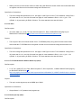
1
PSAS Avionics Node Front End for LV2b Rocket
To:
•
Mark Faust (Academic Adviser)
Andrew Greenberg (Industry Sponsor)
Capstone Team Members:
•
Sarah Bailey - Computer Engineering
Jacob Davidson - Electrical Engineering
Glenn LeBrasseur - Computer Engineering
(16-June-2006)
Table of Contents
1. Introduction
2. (Final) Requirements
3. System Level Design
1. Communications Bus
1. Bus Requirements
2. CAN and USB Comparison
2. Microcontroller
1. Requirements
2. 32-bit Microcontrollers considered
3. ARM Comparison
4. Final Choice
3. RTOS
1. eCos
4. System Block Diagram
1. Block Diagram of Node
2. Switching Power Supply (SPS) Block Diagram
3. ARM and Glue Circuitry Block Diagram
4. Detailed Design
1. Schematics
1. Eagle CAD Schematic of node
2. Board Layout
5. Component Specification
1. SPS
1. Front end Passive Block
2. Circuit Breaker Block
3. Overvoltage Protection
4. Switcher
5. Secondary Voltage Supply
6. Power LED
7. Bill of Materials (BOM)
2. ARM and Glue Circuitry
1. ARM 7 microcontroller (U280)
2. Power decoupling (C285, 286, 287, 288, 291, 292)
3. USB filtering block
4. Power-on reset
5. Oscillator and divider
6. RTC crystal oscillator
7. Debug port
8. Power Good and Shutdown
9. Breakout of signals to application specific area
10. Status LEDs
11. Test points
12. Configuration trace-cuts or solder jumpers
13. Bill of materials (BOM)
6. Software
1. Introduction
2. Tools used
1. Serial Terminal
2. ISP Software
3. Cross-Compiler
3. Serial Port Test
4. "Hello Blinky World!" Example
1. Introduction
2. License Issue
3. Modifications From Original
4. Source Code Review
5. Compiling and Downloading Instructions
6. Results
5. eCos Port
1. Introduction
2. LPC2148 Port
3. Source Code Review
4. Compiling the eCos Demo
5. Downloading Instructions
6. Future Work
7. Construction and Test Plan
1. SPS
1. Front end
2. Circuit breaker (CB)
3. Switcher
4. Overvoltage (OV)
5. Secondary supply
6. Final System block testing
2. ARM and Glue Circuitry
1. Reset Circuitry
2. Crystal Oscillator
3. USB interface
4. ARM + Glue "power up"
5. ARM + Glue final block testing
3. Software
1. Node Testing
2. Initial USB Testing
3. USB Performance Testing
4. Final System Testing
8. References
1. USB
2. Switching Buck Regulator
9. Appendix
1. User Manuals
2006 Capstone Project Final Report
1. Introduction
Our Capstone project was sponsored by the Portland State Aerospace Society. PSAS is a Portland State University
student club that focuses on amateur rocketry projects. Students and industry professionals design and build motors,
airframes, avionics hardware, and write software, all with the end goal of launching an "open source" rocket. All the
designs and software are freely available on the PSAS website, so any amateur group could duplicate our results.
Since the successful but finally disastrous launch of Launch Vehicle No. 2 (LV2), the PSAS Avionics Team has been
redesigning the avionics system. This new system, called the "LV2b" avionics system, should avoid the limitations of the
old system:
•
Replace the Microchip PIC processors, which require Windows-based development tools and a proprietary
commercial compiler, with a more open source microcontroller.
•
Use saner communication protocols: either a more easy-to-use CAN system of IDs, or possibly switch to USB.
The goal of the PSAS Capstone team is to design the generic front-end that interfaces between all the nodes of the
system (GPS, IMU, recovery system, etc) and the communication bus.
2. (Final) Requirements
There are three requirements for completion of our capstone project:
•
an EAGLE schematic for the generic node front-end
•
the EAGLE board layout started and
•
a VERY detailed "engineering notebook" going over each part of the design.
These engineering notebooks should cover the three major areas of design: the Switching Power Supply (SPS), the
microcontroller and glue circuitry, and the software. The notebooks should contain a detailed discussion of how the design
works and an explanation of all component choices and values. A smart, experienced engineer should be able to use this
document to understand why the design is the way it is.
3. System Level Design
3.1. Communications Bus
Part of our capstone project was to decide what communications bus the next generation rocket should use. Numerous
suggestions were thrown out (from FireWire to MIL-STD-1553) but only two communication buses were considered in
depth: the Universal Serial Bus (USB) and the Controller Area Network (CAN) bus.
3.1.1. Bus Requirements
3.1.1.1. Avionics Team Requirements
3.1.1.1.1. Reliability
The bus must be capable of handling EMI, along with short and open conditions on the PHY layer. The bus must tolerate
the acceleration and vibration associated with a launch. The bus should also have been used in real-time systems where
a failure in the bus might result in lives being lost (such as medical equipment or automobiles). The bus must provide a
way for the software to prioritize messages so that system critical messages will be sent, even at the expense of noncritical messages.
3.1.1.1.2. Performance
The bandwidth of the bus must be large enough to keep data flowing and nodes operational. Some nodes will require
access to the bus on regular intervals, while others will be sending non-periodic data packets. The previous rocket's CAN
bus provided 1Mbps, and at most 40% of that bandwidth was used. The bandwidth requirement may change, so more
bandwidth would be better.
3.1.1.2. Software Team Requirements
3.1.1.2.1. High level software control
The Software team would like the high-level software to deal with retransmission of corrupted packets and packets that
were not received by the intended recipient. System critical messages like commands for parachute deployment and
manual overrides from ground support are important to retransmit if a failure occurs. Retransmission of time-based data
like IMU readings is not useful and may eat up the bandwidth of the bus.
3.1.1.2.2. Connectivity
The bus should be able to interface to laptops during testing with minimal difficulty. The communications connectors
should be easy to remove during development and testing, but must lock down during flight. It would also be ideal if the
node controllers could be flashed over the bus.
3.1.1.2.3. Firmware and Device Drivers
The firmware for the node controllers should be maintainable. If there already exists tested bus protocol drivers, it would
be advantageous to use them to minimize the development time and design complexity. Firmware and device driver
development should not require proprietary software or a propriety environment (i.e. Windows).
3.1.2. CAN and USB Comparison
3.1.2.1. Avionics Team Requirements
3.1.2.1.1. Reliability
Both USB and CAN are differential buses, and are more immune to EMI than single-ended buses. CAN is used in some
automobile systems, but not in any systems where failure of the bus alone would result in an accident. USB is used in
some medical devices, but not in life-critical devices.
CAN and USB differ in how they prioritize messages. CAN provides a message-by-message prioritization: when the bus is
idle and two nodes attempt to transmit, the node with a higher prioritization continues to transmit and the other node waits
for the bus to become idle. USB allows the software to reserve bandwidth for each USB endpoint.
USB relies on a host (in our case, the flight computer) to initiate all transactions, even interrupts. This means that if the
flight computer powers off, no messages will flow on the bus. With the CAN peer-to-peer model, the bus would still
operate if the flight computer were offline.
3.1.2.1.2. Performance
CAN provides 1Mbps, and full-speed USB provides 12Mbps.
3.1.2.2. Software Team Requirements
3.1.2.2.1. High Level Software Control
The CAN controller handles packet retransmission automatically. The Software team is concerned about the automatic
retransmission of all corrupted packets. Often we don't want an older time-dependent message (such as an IMU
message) to be retransmitted if it means that we don't receive the newest message. If a high priority node starts sending
lots of corrupted packets, it may flood the bus with automatic retransmissions. This is a remote possibility, but it
demonstrates the inflexibility of the CAN transmission protocol.
USB provides some flexibility when it comes to message retransmission. If the transmitter uses isochronous transfers,
there is no ACK of the message, and corrupted packets are not retransmitted. Isochronous transfers provide guaranteed
bandwidth, and would be ideal for messages from the IMU. Control transfers provide a limited amount of guaranteed
bandwidth (10% of the frame, or more if the isochronous transfers take less than 90% of the bandwidth). They are
acknowledged by the receiver, and automatically retransmitted if the message was not acknowledged or if it was
corrupted. Control transfers would be ideal for system critical messages, such as data from the DTMF receiver board or
commands to the recovery node. Each USB endpoint could be set to a different transfer type.
3.1.2.2.2. Connectivity
A USB communications bus could be directly plugged into a software developer's laptop. CAN requires special conversion
hardware (such as USB to CAN adapters) to interface with a laptop. USB will require a special connector, since the
standard connector does not lock into place. However, CAN has no standard connector, so we will be creating our own
custom connectors anyway.
3.1.2.2.3. Firmware and Device Drivers
The most likely candidate for an open source RTOS is eCos, and the flight computer will run Linux. PSAS members have
experience writing CAN drivers, but they also have local contacts with people who write Linux USB device drivers. There
are many Linux and eCos USB drivers available that could be modified, but few CAN drivers. Linux and eCos both have a
hardware-independent driver framework for USB, but not for CAN.
PSAS members have written CAN drivers, and PSAS has contacts with programmers who have written USB drivers for
Linux. Even if we find a device driver that meets most of our needs, there will probably be some custom "hacking" on it.
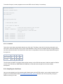
3.1.2.3. Summary
Hardware Requirements
Requirement
CAN
USB
"best" bus
EMI immunity
Differential bus
Differential bus
-
tolerance to over-voltage
built-in
none
CAN
safety critical systems usage automobiles
some medical devices CAN
message priority
individual node priority bandwidth priority
?
bus topology
peer-to-peer
host initiated
?
speed
1Mbps
12Mbps (full speed)
USB
Software Requirements
Requirement
CAN
USB
"best" bus
packet retransmission
automatic
depends on message type
USB
packet size
up to 8 bytes
up to 1023 bytes
USB
connectivity
special connection disrupts debugging plugs in directly to a laptop USB
previous open source drivers very few
good Linux support
USB
As the chart shows, the Avionics team wanted the CAN bus because it provided better hardware reliability and was widely
used in safety critical systems. However, USB was an overall win for the Software team. In the end, the promise of higher
bandwidth and better open source support won over the Avionics team.
3.2. Microcontroller
3.2.1. Requirements
The microcontroller for the node front-end must meet the following requirements:
3.2.1.1. Architecture
•
Must be >= 32 bits.
•
Should have many implementations, by more than one manufacturer if possible.
•
Should have decent integer math ALU (e.g., 32 x 32 -> 64, MAC, etc).
3.2.1.2. Development Tools
•
Must have current and active OSS tools: gcc, gdb, binutils, etc.
•
Must have useful open debugger protocol (e.g., JTAG)
3.2.1.3. Packaging
•
Must have "usable" packaging: packaging that can be used on two layer boards.
o
Must be a "Quad Flat Pack" (or QFP, e.g. a TQFP or LQFP), or possibly a BGA with < 32 pins.
o
QFP should have <= 64 pins. >= 100 pins is possible but a pain. 144 pins absolute maximum.
3.2.1.4. Peripherals
•
Must have on board memory: >= 128 KB flash, >= 32 KB SRAM.
•
Must have necessary communication buses (CAN and/or USB).
•
Should have one or more serial buses: UART, SPI, etc.
•
Should have a >= 10 bit ADC.
•
Should have >= 3 PWMs.
•
Should have a watchdog timer.
•
Should have brown out reset.
3.2.1.5. Computational Horsepower
•
Must have > 10 MIPS, but should have >= 60 MIPS.
3.2.1.6. Power Consumption
•
Should have reasonable voltage requirements (e.g., 3.3V only (best) or 3.3V/5V).
•
Should have low power modes.
3.2.1.7. Cost
•
Should be relatively low cost in small quantities.
3.2.2. 32-bit Microcontrollers considered
There were two microcontroller architectures considered initially: ARM (Advanced RISC Machine) and PPC (Power PC).
ARMs are popular microcontrollers with good open source support. On the other hand, PSAS has a grant from IBM to use
Power PC microcontrollers on the rocket. A quick look at PPC manufactures revealed the microcontrollers did not meet
our package size requirements; the smallest package size available was a 168 pin BGA.
3.2.3. ARM Comparison
The capstone team searched the websites of over 34 companies that license the ARM core. Of those companies, only
five had microcontrollers with CAN or USB: Atmel, Freescale, Philips, STMicroelectronics, and Texas Instruments.
There were roughly 30 chips that met our requirements. We compared the 30 chips, looking at various characteristics,
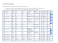
such as package size, speed, memory, and peripherals. For the full comparison chart, see the file
NodeMicrocontrollerSearch/ARMs.xls
There were 11 microcontrollers that best met our requirements: 5 had both CAN and USB, 3 had CAN only, and 3 had
USB only. The microcontrollers that had both CAN and USB were all 100 pin packages from Atmel. Once we looked at
drawings of pin package sizes compared to our required board size, we realized that we simply couldn't fit a 100 pin
package on the board. That only left the 64-pin CAN only or USB only microcontrollers.
When the decision was made to use USB in the next generation rocket, we took a look at the USB only ARM chips. There
were three top choices: an Atmel AT91SAM7S256, the Philips LPC2148, and the STM STR711FR2T6.
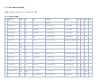
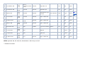
3.2.3.1. Comparison Chart
Characteristic
Atmel
Philips
STM
production status
production sampling active
SRAM (KB)
64
40
64
flash (KB)
256
512
256
frequency (MHz)
55
60
66
JTAG
Y
Y
Y
serial boot
N
Y
?
A/D bits
10
10
12
number of ADCs
8
14
4
max number of GPIO pins 32
45
30
UARTs
3
2
4
SPIs
1
2
2
I2C
1
2
2
16 bit timers
3
4
4
PWM channels
4
3
4
Watch dog reset
Y
Y
Y
brown out reset
Y
Y
?
power on reset
Y
Y
?
RTC
Y
Y
N
3.2.3.2. Miscellaneous "Warts" Found
3.2.3.2.1. Atmel
To use USB, the system designer is forced to under clock the microcontroller at 48MHz. It also doesn't have a real-time
clock (only a real-time timer). The Atmel chip was discarded early in the selection process because of USB issues (see
below).
3.2.3.2.2. Philips
Philips was lacking in memory, and the quoted SRAM size of 40KB is deceptive. There is 32KB of SRAM for general use,
but 8KB of that is reserved for USB. That puts it on the lower limits of our memory requirements.
The Philips part exclusively uses an internal 1.8V voltage regulator, which means we can't hook up our switching power
supply. This increases the power consumption of the system.
Also, the pin multiplexing may prove troublesome. When PSAS designs a self-correcting rocket, all three PWMs will be
used on a node to control motor servos. The PWMs on the LPC2148 conflict with other devices we want to use, such as
SPI and UART0. However, this need is far in the future and we may switch to a new microcontroller before then.
3.2.3.2.3. STM
The STM part also requires the microcontroller to be run at 48MHz to use USB.
Another wart was that the ADC conversion time is listed as 1ms. This was unacceptable, considering that the other two
microcontrollers listed 2us conversion times. The PLL lock time also seemed to be a bit long; it was listed as 600us, while
Philips listed a 100us lock time. Further, the internal oscillator takes 2.5 seconds to start up. If the microcontroller has to
do a hard restart in flight, we would lose half of the apogee window to oscillator initialization.
Also, the data sheet was vague about whether the internal voltage regulator could be bypassed in Standby mode.
3.2.3.3. USB Considerations
The STM documentation for USB was severely lacking. Their datasheet did not indicate how many of each type of USB
endpoint were available. The lack of documentation made this an unacceptable choice.
The Atmel part only had four USB endpoints; two endpoints could be configured to be isochronous endpoints. They also
listed endpoint 0 as being able to send control, bulk, or interrupt transfers. This seemed to be an indication they were
doing something out of spec with their USB controller, since the USB specification clearly states that endpoint 0 must be
reserved for control transfers from the host.
The Philips chip had the best documentation of the three chips, and it had the most endpoints. The LPC2148 had 16 USB
endpoints and 4 endpoints could be configured to be isochronous endpoints.
3.2.4. Final Choice
In the end, we decided to choose the Philips LPC2148 chip because of its great documentation and USB support.
3.3. RTOS
A program with real-time requirements will need a real-time operating system. With a standard operating system, there is
no guarantee that time constraints of a program will be met. This is disastrous in an avionics system, when a delay in
sensor data or recovery node commands may mean the parachute is not deployed in the 5 second apogee window.
RTOS Requirements:
•
Hard real-time performance
•
Fully open-source
•
Small footprint
•
Ported to several ARM processors
•
Integrated debugging tools (GDB)
There were two RTOS that fit all requirements: eCos (
http://ecos.sourceware.org/) and FreeRTOS (
http://www.freertos.org/). PSAS members have more experience with eCos, so eCos was chosen.
3.3.1. eCos
eCos stands for "embedded Configurable operating system". eCos is configurable because you can choose which
features you want to compile into your embedded operating system. This allows you to tweak your options if you don't
have a lot of memory in your embedded system. For example, a programmer can choose to compile GDB stubs into their
program and eCos. This is great for debugging, but can inflate the code size. After the person is done coding and wants to
run the program out in the field, they can recompile eCos without GDB stubs to save memory.
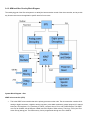
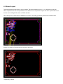
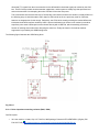
3.4. System Block Diagram
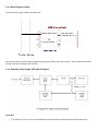
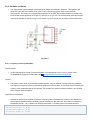
Here is the new avionics system design:
3.4.1. Block Diagram of Node
The scope of this project is within the dashed line.
Each generic node front-end contains a switching power supply (SPS), some "glue circuitry", and an ARM microcontroller
running a real-time operating system (RTOS).
3.4.2. Switching Power Supply (SPS) Block Diagram
Power Bus
•
This is the 16.8 V (four 4.2 V Li-Ion cell batteries) power bus where all LV2b nodes derives their power from.
Front end Passive Block
•
This block acts as a high frequency electromagnetic interference (EMI) filter using an input choke and bypass
capacitors. Also there are two protection features in this block: (1) fuse and (2) input overvoltage protection. There
is a DC path between the SPS ground and the rocket’s chassis.
Circuit Breaker Block
•
This block protects the SPS from overcurrent events. The maximum specified output current is 400 mA. If there is
an overcurrent draw below the rated fuse current (500 mA) or if the fuse fails to blow or opens in a longer amount
of time this block will disconnect the rest of the SPS from the power bus. The only allowable and designed for
component that should ever be destroyed in a fault event is the fuse. This block also is the first stage in under
voltage lockout (UVLO) protection. If the voltage on the power bus is below 9 V this block will disconnect the rest
of the SPS from the power bus.
Overvoltage Protection Block
•
This block protects the SPS from overvoltage at the SPS out, meaning if the +3.3 V SPS rail tries to increase past
a certain threshold this block will engage the circuit breaker block which will disconnect the rest of the SPS from
the power bus. It is powered by the SPS output itself but has the ability to be powered for a finite amount of time
(0.5 s) while the SPS rail is zero volts.
Switcher
•
This is the switching voltage regulator block. It specifically is a buck topology. This block regulates the power bus
voltage (its input is slightly less than the power bus voltage) to the specified +3.3 V SPS voltage.
+3.3 V SPS
•
This is the output of the SPS which powers all 3.3 V parts on the nodes. It is specified as a +3.3 V @ 400 mA
(max) power supply.
Power LED
•
This block only indicates if the +3.3 V SPS rail is up. It lights an LED to signify this. The LED is on as long as the
SPS is on. This block is only useful when a user is trouble shooting the SPS (opened LV2b rocket) on the ground.
Secondary Voltage Supply
•
This block acts as a secondary buck supply where it “taps” the buck output inductor in the Switcher block. Another
low dropout (LDO) regualtor could possibly further regulate its voltage down to 5 V since it will not be 5 V. This
block is included in the SPS design because certain nodes in the LV2b will use parts, specifically analog-to-digital
converters (ADC), which are 5 V parts. This secondary buck regulator will regulate the tapped Switcher voltage
down to something around 7.2 V which again can be regulated be a LDO for the ADC’s use.
3.4.3. ARM and Glue Circuitry Block Diagram
The underlying goal of the Glue subsystem is to satisfy the interconnection needs of the microcontroller, and to provide
any forseen resources to the application specific area for future users.
System Block Diagram - Glue
ARM7 microcontroller (CPU)
•
This is the ARM7 microcontroller that is the primary processor on the node. The microcontroller contains 10 bit
analog to digital converters, a digital to analog converter, pulse width modulators, general purpose I/O, external
interrupts, SPI interfaces, I^2 C interfaces, 2 UARTs, counters, timers, PLLs, and a USB interface. The ARM7
core runs at 60 MIPS, has 40 K Bytes of RAM, and 512 K Bytes of flash memory. There is a JTAG (Joint Test
Action Group) debug port. The flash memory can be programmed through one of the UARTS.
Power decoupling
•
This block provides transient decoupling between switching power supply and the logic power. The block also
provides a single point ground connection between the analog ground bus and the SPS ground.
USB filtering block
•
This block provides EMI and RF suppression from noize that might be picked up from the external USB bus.
There is also 10 kV of surge suppression, current limiting, power decoupling, and a single point connection
between IO ground and the SPS ground. Finally this block provides the 1.5 k ohm pullup to indicate this endpoint
is to use USB full speed.
Power-on reset
•
This block provides the reset signal required by the microcontroller. The reset is released after the SPS has come
up to the proper operating voltage, and after the time required by the microcontroller to assure it is running
properly.
Oscillator and divider
•
This block provides the 12.0 MHz for the microcontroller system clock. Part of this block is contained within the
microcontroller. This block also divides down the 12.0 MHZ by 8 to create a 1.5 MHz clock to syncronize the SPS.
This SPS syncronization assures that switching noize created by the SPS remains constant and at a known
frequency allowing it to be more easily filtered out should it cause problems with any of the circuits later down the
road.
RTC crystal oscillator
•
This block provides the 32.768 kHz clock signal used by the microcontrollers real-time clock. This block also
contains the clock power to maintain the time of day clock when the node power is off.
Debug port
•
This is an external connector providing standard JTAG (Joint Test Action Group) debug signals. The port also
provides access to the UART used for programming the on-chip flash memory. There is also 3.3 volt power and
digital ground provided on this port should a special debug feature need it.
Power Good and Shutdown
•
These signals between the microcontroller and SPS will (1) allow the microcontroller to detect a good/bad power
condition so it could do some possible corrective or evasive action, and (2) allow the microcontroller to shut down
the node power in case of emergency or the need for a power-up reset. The hot-swap controller (circuit breaker
block) will reset and restart the SPS after a specific period of time provided the external power is still acceptable.
Breakout of signals to application specific area
•
This is where the future application specific portion of the node accesses the resources provided by this front-end
module.
Status LEDs
•
These are simple Red and Green LED's driven by microcontroller general purpose IO. The intent is to provide a
future user defined status indicator for what ever reason.
Test points
•
There are test points identified on the schematic and board intended for validation of specific functions, such as
SPS Sync Clock, Power Good, SPS Shutdown. These typically would be used during initial testing, but my be of
use later when the application specific functions are being tested and debugged.
Configuration trace-cuts or solder jumpers
•
There are jumpers that can be reconfigured by doing a physical trace cut, and resolder. The configuration
changes are for analog reference voltage source, and clock battery voltage source.
4. Detailed Design
4.1. Schematics
4.1.1. Eagle CAD Schematic of node
The schematics used in the design of this project appear in two forms; one for the Spice circuit simulator, and another for
the Eagle CAD PCB board layout tool. This section only shows the Eagle CAD schematic. The Spice schematic was used
for verification of the SPS design, and can be found in that section.
•
•
[get | view] (290.6 KB) attachment:gnl_schem.png
[get | view] (160.6 KB) attachment:gnl_schem_small.png
4.1.1.1. Naming convention
The name of this project according to PSAS convention is:
•
node4 = USB Node v4, which is the (ARM7 + SPS v2) 2006 capstone design
So the name of this board is: lv2-node4-frontend
4.1.1.2. Getting the Eagle CAD board layout tool
Go to the Eagle CAD site (
http://www.eagle.de) and follow the instructions under downloads for your specific platform.
For this project we used the Debian Linux distribution, and thereby were able to use Debian's package management tool
called Aptitude. The following command on a Debian Linux system installs the Eagle CAD software package.
sudo apt-get install eagle
4.1.1.3. Getting the Eagle schematic files for this project
The schematic files for this project are kept in the PSAS Subversion source repository. The following Linux command
checks out the CAD sub-tree from the repository which includes the node-4 files, and needed libraries. To find out more
about Subversion see: < http://subversion.tigris.org/>
svn co http://svn.psas.pdx.edu/svn/psas/trunk/cad
The above command will check out the entire PSAS cad directory. The files you will actually need for this project are:
•
libraries/psas-eagle-library.lbr : This is the standard PSAS parts library
•
lv2-node4-frontend/node4-frontend.sch : This is the schematic od the project as seen above.
•
lv2-node4-frontend/node4-frontend.brd : This is the board layout.
•
lv2-node4-frontend/node4.lbr : This is a library of special parts used in this design.
It is intended that eventually the <node4.lbr> library be merged into the <psas-eagle-library.lbr> library at a future time.
4.1.1.4. Maintaining the files
To maintain the schematics, be sure you have latest copies before starting by doing an update command. Once your
changes are made, check them into the repository using the check-in command.
svn up
# get latest update
svn ci
# check-in your latest work
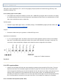
4.2. Board Layout
This is the preliminary board layout; it is not complete. The board dimensions are 2 in. x 3 in. with traces on only two
sides. Components are also on top and bottom. The decision to use only two trace layers was driven by the desire to use
the free version of Eagle CAD, which is a PSAS standard.
On the left top side of the board is the USB/Power connector. The Debug port will be placed on the left bottom side.
Both top and bottom of board shown with component placemets
Top side only of board
Bottom side only of board
5. Component Specification
5.1. SPS
SPS_Design_Schematic_rev2_2.pdf
Note: It is easier to refer to the schematic above when reading section 1.5.1 instead of the detailed Eagle schematic in
section 1.4.1.1. This is because this section exclusively covers all SPS components. The part numbers are consistent with
those in the Eagle schematic.
5.1.1. Front end Passive Block
5.1.1.1. Power Bus Input Choke (L201a, L201b)
Part Description:
•
CMS1-11-R Common Mode Inductors 100 uH, Micro-PAC Plus Package, RoHS Compliant, Tape and Reel.
http://www.cooperet.com/library/products/PM-4313%20CMS-Series.pdf.
Purpose:
•
Common mode choke (balanced inductor). It is used as an EMI filter between the power bus and the SPS.
Specifications/ Calculations:
•
The value was chosen through a trial and error process from the pervious LV2 SPS design. Each inductor of the
choke is 100 uH. See page 13 of the CAN Node Switch Mode Power Supply (SPS) (200) section in the
Component Design for LV2 Power Electronics (Except Main Battery) engineering design notes.
5.1.1.2. Power Bus Fast-Acting Fuse (F200)
Part Description:
•
500 mA, 50 V, 1206, Fast Acting Short Time Lag, RoHS Compliant, Wickmann USA Inc, FCD120500TP (Digi-Key
p/n WK6213CT-ND $0.56/1)
http://rocky.digikey.com/WebLib/WICKMANN/Web%20Data/FCD12.pdf.
Purpose:
•
This fuse protects the SPS from currents greater than 500 mA. Its direct purpose however is to protect the power
bus from a short circuit fault on the SPS side.
Specifications/ Calculations:
•
Since the specified maximum SPS current is 400 mA we chose a fuse rated at 500 mA. The opening time for the
fuse according to its datasheet is 1 s at a current of about 1.15 A. Currents below 1 A are several hundred
seconds, therefore this fuse will only protect the SPS or power bus from gross currents due to some fault on
either side (power bus or SPS) and not to keep the SPS output current within spec, that is U250's job.
5.1.1.3. DC Path From SPS Node GND to Chassis GND Resistor (R215)
Part Description:
•
100 kohm, 0805, 1%, 1/8 W, Cut Tape, RoHS Compliant, Rohm, MCR10EZHF1003 (Digi-Key p/n RHM100KCCTND $0.38/10)
http://www.rohm.com/products/databook/r/pdf/mcr10.pdf.
Purpose:
•
R215 provides a DC path from the SPS ground to chassis ground. See page 29 of the CAN Node Switch Mode
Power Supply (SPS) (200) section in the Component Design for LV2 Power Electronics (Except Main Battery)
engineering design notes.
Specifications/ Calculations:
•
100 kohm worked.
5.1.1.4. Power Bus Input Caps (C203, C204)
5.1.1.4.1. C203
Part Description:
•
22 uF, 25 V, Tant, T491 Series, 7343-31 (EIA), Cut Tape, RoHS Compliant???, Kemet, T491D226K025AT (DigiKey p/n 399-3782-1-ND $0.65/1)
http://www.kemet.com/kemet/web/homepage/kechome.nsf/vapubfiles/F3102T491.pdf/$file/F3102T491.pdf.
Purpose:
•
C203 acts as a noise filter between the power bus and SPS. It also serves as a local energy storage node.
Specifications/ Calculations:
•
It needs to have a voltage rating greater than 20 V and a low equivalent series resistance (ESR) thus a tantalum
capacitor was chosen due to their low ESR at a higher capacitance.
5.1.1.4.2. C204
Part Description:
•
0.33 uF, 50 V, 0805, X7R, Cut Tape, RoHS Compliant, Murata Electronics North America ,
GRM219R71H334KA88D (Digi-Key p/n 490-3327-1-ND $3.09/10)
http://search.murata.co.jp/Ceramy/image/img/PDF/ENG/GRM219R71H334KA88.pdf.
Purpose:
•
C204 is a high frequency noise filter between the power bus and SPS. It did not have to have as high a
capacitance as C203 so the trade off was to get a lower value at a low ESR.
Specifications/ Calculations:
•
It needs to have a voltage rating greater than 20 V and the capacitance value was not very critical but should be
much lower than C203.
5.1.1.5. Power Bus Input Voltage Suppressor (TVS200)
Part Description:
•
18 V, SMB, Unidirectional, Cut Tape, RoHS Non-Compliant, Diodes Inc, SMBJ18A-13 (Digi-Key p/n
SMBJ18ADICT-ND $0.89/1)
http://www.diodes.com/datasheets/ds19002.pdf.
Purpose:
•
A transient voltage suppressor (TVS), this "zener like" diode protects the SPS (specifically U200) in the event of
an overvoltage at the input.
Specifications/ Calculations:
•
It should have a breakdown voltage of about 20 V (unlikely maximum bus voltage) and a current carrying capacity
greater than the fuse rated current. It should have a fast response time and be unidirectional. In the event of a
sustained overvoltage at the input the only allowable part which can be destroyed is the fuse, F200. That is what
we want.
5.1.2. Circuit Breaker Block
5.1.2.1. MAX5902 Circuit-Breaker Resistor Network (R250, R251)
5.1.2.1.1. R250
Part Description:
•
61.9 kohm, 0805, 1%, 1/8 W, Cut Tape, RoHS Compliant???, Rohm, MCR10EZHF6192 (Digi-Key p/n
RHM61.9KCCT-ND $0.38/10)
http://www.rohm.com/products/databook/r/pdf/mcr10.pdf.
Purpose:
•
R250 is part of the UVLO resistor divider of U250.
Specifications/ Calculations:
•
The UVLO voltage was specified to be 9 V. See page 8 and Figure 3 in the MAX5902 datasheet. Letting R251 =
10.0 kohm and using the typical value of Von/!off = 1.26 V, the UVLO formula from page 8 in the datasheet is R250
= R251 * ((VUVLO / (Von/!off)) - 1) = 61.4 kohm. The closet standard value was 61.9 kohm.
5.1.2.1.2. R251
Part Description:
•
10.0 kohm, 0805, 1%, 1/8 W, Cut Tape, RoHS Compliant???, Rohm, MCR10EZHF1002 (Digi-Key p/n
RHM10.0KCCT-ND $0.38/10)
http://www.rohm.com/products/databook/r/pdf/mcr10.pdf.
Purpose:
•
R251 is part of the UVLO resistor divider of U250.
Specifications/ Calculations:
•
R251 was specified to be 10.0 kohm. See page 8 and Figure 3 in the MAX5902 datasheet.
5.1.2.2. Overcurrent/Circuit-Breaker Protection (U250)
Part Description:
•
MAX5902AAETT +72 V, SOT-23, Simple Swapper How-Swap Controller. Ordered samples from vendor, no DigiKey.
http://pdfserv.maxim-ic.com/en/ds/MAX5902-MAX5903.pdf.
Purpose:
•
This hot-swap controller IC serves two purposes: (1) circuit-breaker and (2) the first stage of UVLO protection.
The version we chose had a input voltage range of +9 V to +72 V, a 300 mV circuit-breaker threshold voltage,
limited inrush current ("soft start") and was an automatic retry circuit-breaker. It also had a built-in thermal
shutdown and active low power good (!PGOOD) indicator output pin. The device needed a UVLO resistor divider
network (R250, R251) and an external PMOSFET (Q250) switch.
There are four events which will cause Q250 to turn off: (1) if there is undervoltage at the input, (2) if there is
overcurrent, (3) if the die temperature exceeds +125 C and (4) the ON/!OFF pin 6 is forced low for at least 10 ms.
See the MAX5902 datasheet.
Specifications/ Calculations:
•
The reasons we chose the 300 mV automatic retry circuit breaker version was that we wanted the SPS to be able
to recover from a fault condition by itself and we expect that the nominal load current will not be very close to the
400 mA maximum limit but closer to 300 mA or less. Hence steady-state currents in the range of 400 mA to 500
mA qualify as an overcurrent event and should be detected. To avoid wasting power dissipated by Q250's
RDS(on) and R252, those values should be kept low, therefore the voltage across them should also be low and
the 300 mV threshold version satisfied that.
Upon power up U250 keeps Q250 off and if trigger events (1) and (2) are non-existent, then it gradually turns
Q250 on to saturation in approximately 150 ms. The drain of Q250 is gradually enhanced at a rate of about 9 V/
ms. This start sequence limits the inrush current giving some "soft-start" protection to its load. Once all transients
are gone before the 150ms time period and Q250 is fully saturated, U250's circuit-breaker functionality comes up
and monitors the Vds of Q250 between pins 1 and 2. Before this initial power up 150 ms period there is no circuitbreaker functionality. If any one of the 4 trigger events occurs U250 will turn Q250 off, de-assert !PGOOD (output
a logic high) and reinitiate the start sequence given that the trigger event(s) disappears during the 150 ms period,
if not the 150 ms period will repeat.
There are two typical turn off times regarding Q250: 10 ms and 4 us. If there is an ON/!OFF or UVLO trigger
event, they need to exist for 10 ms before U250 turns Q250 off, which will take an unspecified amount of time. If
there is an overcurrent or temperature trigger event, then Q250 is turned off in 4 us. If the trigger events
disappear after Q250 turns off within 150 ms, then the normal start sequence is reinitiated.
Since the purpose of U250 was to be a circuit-breaker we decided not to use the ON/!OFF pin to turn Q250 off via
any SPS feedback. Only an UVLO condition would be a trigger event. The UVLO threshold was specified as 9 V.
See R250 and R251. This meant that when a trigger event other than a UVLO condition happens, U250 would
turn Q250 off in 4 us and would reinitiate the start sequence after a trigger event free 150 ms time period.
We needed a way for the LPC2148 (U280) microcontroller to turn off the SPS, so we connected a logic level
NMOSFET (Q282) to a GPIO pin and connected the drain of Q282 to the ON/!OFF pin of U250. Also we
connected the active low !PGOOD pin to another GPIO pin for monitoring and/or interrupt purposes. See the
GLUE Logic section regarding U280 and Q282.
See R253 and Q251 for the "overvoltage to overcurrent" trigger event emulation.
One bad thing that we did not like was the relatively high supply current of U250 being 1 mA to 2 mA. We believe
that U250 will draw the most current from the power bus when the SPS is in a standby/shutdown mode.
NOTE: According to the MAX5902 datasheet there are two package options for the different versions of the
MAX5902: a TDFN and SOT23 package. All SOT23 packages have the specification that, "This device is
constructed using a unique set of packaging techniques that impose a limit on the thermal profile the device can
be exposed to during board level solder attach and rework. This limit permits only the use of solder profiles
recommended in the industry standard specification, JEDEC 020A, paragraph 7.6, Table 3 for IR/VPR and
convection reflow. Preheating is required. Hand or wave soldering is not allowed.", which may or may not present
a problem. The invoice we received for the ordered samples specified that they were MAX5902AAETT+ in a
SOT23 package (they were in the SOT23 package). The datasheet however specifies that the MAX5902AAETT
is a TDFN part (which does not have a special solder specification) and all SOT23 part numbers have the "*"
symbol suffix. The "+" symbol suffix in the invoice means its a lead-free part. There are some discrepencies.
5.1.2.3. MAX5902 External P-MOSFET (Q250)
Part Description:
•
-60 V, -3 A, SOT-23-6, P-Channel MOSFET, Cut Tape, RoHS Compliant, Zetex Inc, ZXMP6A17E6TA (Digi-Key
p/n ZXMP6A17E6CT-ND $1.04/1)
http://www.zetex.com/3.0/pdf/ZXMP6A17E6.pdf.
Purpose:
•
This is the external PMOSFET of U250 which will turn off given that there is one or more of the four trigger events
as described earlier. See U250. U250 uses the RDS(on) of the saturated Q250 as a current sense resistor which
generates a Vds voltage which is detected across the Vs (Pin 1) and DRAIN (Pin 2) pins and if it is greater than
some threshold voltage, U250 will switch Q250 off thus breaking the circuit.
Specifications/ Calculations:
•
The maximum SPS output current specified was 400 mA. There are three circuit-breaker threshold voltage
versions of U250: 300 mV, 400 mV and 500 mV. For certain reasons the 300 mV threshold part was chosen. See
U250. Therefore the RDS(on) of the PMOS should be around 300 mV / 400 mA = 0.75 ohm. We used a value of 1
ohm. See R252.
Even though the PMOS is used as a switch (cutoff and saturation) and not an amplifier (cutoff, triode and
saturation) we wanted to remove dependence of U250's threshold voltage detection from the less precise RDS(on)
of Q250 and to a more precise sense resistor. Therefore we added a current sense resistor (R252) in series with
the drain of Q250 to produce a circuit-breaker resistor, Rcb, which is the series combination of Q250's RDS(on) and
R252 between the two pins 1 and 2 of U250. We chose a PMOS with a low RDS(on) compared to the needed
calculated value needed to trip the circuit-breaker thereby making R252 close to Rcb in value. Therefore Q250 is
used mostly as a switch and the voltage drop across R252 is used to trigger the switch. See R252.
The breakdown voltage of Q250 has to be greater than 20 V and should have a low "turn on" capacitance. We do
not care so much about the Vt but it does affect the "turn on" capacitance but these factors were not considered.
5.1.2.4. MAX5902AAETT Circuit-Breaker External P-MOSFET RDS(on) Additional Series Resistor (R252)
Part Description:
•
0.82 ohm, 0805, 1%, 1/8 W, Cut Tape, RoHS Compliant???, Panasonic - ECG, ERJ-6RQFR82V (Digi-Key p/n
P.82DCT-ND $2.10/10)
http://www.panasonic.com/industrial/components/pdf/AOA0000CE3.pdf.
Purpose:
•
This resistor dominates the circuit-breaker resistor's (Rcb) value. It is in series with the drain (hence RDS(on) of
Q250 to make up Rcb. The voltage drop across it is used to detect an overcurrent event given that it is greater
than 300 mV. See Q250 and U250. Note: This value may change due to board level testing results.
Specifications/ Calculations:
•
Since the typical value of RDS(on) of Q250 is 0.125 ohm and Rcb was about equal to 1 ohm, R252 = Rcb - RDS(on) =
0.875 ohm. The closet standard value was 0.82 ohm. Given this value of Rcb and the circuit-breaker trip threshold
voltage of 300 mV, the maximum SPS current which can be drawn before an overcurrent event is Imax = 300 mV /
(0.125 ohm + 0.82 ohm) = 317 mA which is under the specified maximum SPS current spec.
5.1.3. Overvoltage Protection
5.1.3.1. Undervoltage/Overvoltage Protection (U251)
Part Description:
•
Nanopower Push-Pull Output Comparator with Voltage Reference, 1.8 V < Vin < 5.5 V, SOT-23-6, Tape & Reel
(TR), RoHS Compliant, Texas Instruments, TLV3012AIDBVT (Digi-Key p/n 296-16830-2-ND $262.50/250) NOTE:
Ordered samples from vendor no Digi-Key.
http://focus.ti.com/lit/ds/symlink/tlv3012.pdf.
Purpose:
•
This comparator compares the specified divided SPS output voltage (see R254, R255) to its internal reference
voltage (1.242 V) for an overvoltage trigger event at the SPS output. It is powered by a secondary supply
consisting of CR250 and C250. Also it has a pseudo low-pass filter consisting of C251 and its output (pin 1) with
the input being pin IN+ (pin 3). See CR250, C250 and C251 respectively.
Specifications/ Calculations:
•
We wanted a low power push-pull output comparator to get rail to rail output swing (approximately 200 mV to 3.1
V) and have reasonable switching and rise/fall times, on the order of several microseconds and nanoseconds
respectively.
We tied the IN- pin (pin 4) to the internal reference voltage REF pin (pin 5) which will be compared to the divided
SPS output voltage at its IN+ pin (pin 3). See R254, R255 and C251. The "undervoltage" protection is actually
provided by CR250 and C250 where U251 will remain powered for a specified amount of time if the +3.3 V SPS
output rail drops. See CR250 and C250.
5.1.3.2. TLV3012AIDBVT Overvoltage Detection External N-MOSFET Current Limiting Resistor (R253)
Part Description:
•
47.0 kohm, 0805, 1%, 1/8 W, Cut Tape, RoHS Compliant???, Rohm, MCR10EZHF4702 (Digi-Key p/n
RHM47.0KCCT-ND $0.38/10)
http://www.rohm.com/products/databook/r/pdf/mcr10.pdf.
Purpose:
•
R253 along with Q251 will "emulate" an overcurrent trigger event as seen by U250 when an overvoltage at the
SPS output trigger event as seen by U251 occurs. See Q251.
When the SPS +3.3 V output rises above a certain threshold, the output of U251 goes high, turning Q251 on.
When this happens it pulls pin 2 of U250 very close to ground and current flows through R253 and Q251. Now
that pin 2 is close to ground and pin 1 is normally close to the power bus voltage this is much greater than 300
mV this causing an overcurrent trigger event for U250. R253 limits the extra current pulled through Q251 when it
is turned on.
Specifications/ Calculations:
•
In normal SPS operation, the voltage drop across Rcb will be less than 300 mV and R253 is connected to the
high impedance pin 2 of U250 so no current flows through it. If there is an overvoltage trigger event at the SPS
output, Q251 is turned on conducting current through R253 which will have a voltage drop of approximately 300
mV less than the power bus voltage: VR253 = 16.8 V - 300 mV = 16.5 V. This results in a current boost of about
IR253 = 16.5 V / 47 kohm = 351 uA which is negligible.
5.1.3.3. TLV3012AIDBVT External Logic-Level N-MOSFET (Q251)
Part Description:
•
100 V, 170 mA, RDS(on) = 10 ohm @ Vgs = 4.5V, SOT-23, Cut Tape, RoHS Compliant???, N-Channel LogicLevel MOSFET, Infineon Technologies, BSS123E6327 (Digi-Key p/n BSS123INCT-ND $0.36/1)
http://rocky.digikey.com/WebLib/Infineon/Web%20Data/BSS123.pdf.
Purpose:
•
This is a logic-level NMOSFET. When an overvoltage at the +3.3 V SPS output occurs, U251 will output a logic
high turning Q251 on and thus conducting current through R253. The current flowing through R253 also flows
through Rcb and its magnitude is dependent on the value of R253 and the bus voltage at the time (nominal value
of 16.8 V).
When there is no overvoltage at the +3.3 V SPS output U251 outputs a logic low thus keeping Q251 off.
Specifications/ Calculations:
•
Since the gate of this FET would be driven by the output of a comparator in U251 it would be best for the FET to
be a logic-level device. Other concerns was for the drain-source breakdown voltage to be higher than 30 V as the
highest possible DC value the bus voltage rail would be is 20 V.
5.1.3.4. TLV3012AIDBVT UVLO Lockout Resistor Network (R254, R255)
5.1.3.4.1. R254
Part Description:
•
18.2 kohm, 0805, 1%, 1/8 W, Cut Tape, RoHS Compliant???, Rohm, MCR10EZHF1822 (Digi-Key p/n
RHM18.2KCCT-ND $0.38/10)
http://www.rohm.com/products/databook/r/pdf/mcr10.pdf.
Purpose:
•
R254 along with R255 form a voltage divider with respect to the +3.3 V SPS output rail. When there is an
overvoltage at the +3.3 V SPS output the voltage at the IN- pin (pin 4) of U251 will be greater than the internal
reference voltage of U251 (typically 1.242 V) and will result in the comparator in U251 outputing a logic high
value. When the SPS output is below a certain threshold the input voltage (pin 4) to U251 is less than the internal
reference voltage and the comparator's output is a logic low.
Specifications/ Calculations:
•
From the LPC2148 datasheet the maximum supply voltage it can handle is 3.6 V therefore we specified that if the
+3.3 V SPS output was to reach 3.5 V we would want this to qualify as an overvoltage trigger event. Since we
have been using several 10.0 kohm resistors we specified R255 to be 10.0 kohm. Therefore using the
overvoltage trigger event value to be 3.5 V and the compared voltage to be 1.242 V we solved for R254:
1.242 V = (3.5 V * R255)/ (R255 + R254) and solving for R254 = 18.18 kohm. The closet standard value was 18.2
kohm.
5.1.3.4.2. R255
Part Description:
•
10.0 kohm, 0805, 1%, 1/8 W, Cut Tape, RoHS Compliant???, Rohm, MCR10EZHF1002 (Digi-Key p/n
RHM10.0KCCT-ND $0.38/10)
http://www.rohm.com/products/databook/r/pdf/mcr10.pdf.
Purpose:
•
R255 along with R254 form a voltage divider with respect to the +3.3 V SPS output rail. When there is an
overvoltage at the +3.3 V SPS output the voltage at the IN- pin (pin 4) of U251 will be greater than the internal
reference voltage of U251 (typically 1.242 V) and will result in the comparator in U251 outputing a logic high
value. When the SPS output is below a certain threshold the input voltage (pin 4) to U251 is less than the internal
reference voltage and the comparator's output is a logic low.
Specifications/ Calculations:
•
We specified R255 = 10.0 kohm. See R254.
5.1.3.5. TLV3012AIDBVT "Secondary Power Supply" Schottky Diode (CR250)
Part Description:
•
30 V, 1.5 A, 4 ns, New MiniPower 2P, Cut Tape, RoHS Compliant???, Panasonic - SSG, MA2Q70500L (Digi-Key
p/n MA2Q70500LCT-ND $0.83/1)
http://www.semicon.panasonic.co.jp/ds/eng/SKH00017BED.pdf.
Purpose:
•
CR250 and C250 form U251's power supply. This diode prevents C250 from discharging anywhere but to the V+
supply pin of U251. U251 is indirectly powered by the +3.3 V SPS rail. Pin 6 (V+) of U251 will be charged to a
value very close to the +3.3 V SPS rail. As U251 draws more current when needed and its V+ voltage drops
CR250's Vf below the SPS voltage CR250 will re-charge C250. Therefore the average DC current through CR250
is not easily calculable but will be on the order of tens to hundreds of uA. Schottky diodes were chosen for their
fast switching and reverse recovery times.
In response to a overvoltage event at the +3.3 V SPS output, U251 will output a logic high and turn Q251 on
which will cause an overcurrent event at U250 which will in response turn Q250 off thus circuit breaking the bus
rail from the SPS and the +3.3 V SPS output voltage rail will go to zero. That is the sequence of events without
delay times. This is the way U251 emulates an overcurrent event from an overvoltage event.
Specifications/ Calculations:
•
CR250 has a low forward voltage and U251 has an input voltage supply range of 1.8 V to 5.0 V so when the SPS
voltage is being brought up C250 is being charged through CR250 leaving the voltage of SPS minus the Vf of
CR250 at pin 6 (V+) of U251: V+ = 3.3 V - 0.05 V = 3.25 V (approximately). See the first graph on page 2 of the
MA2Q705 datasheet given that the steady state nominal forward current through CR250 < 1 mA. See C250.
5.1.3.6. TLV3012AIDBVT "Secondary Power Supply" Cap (C250)
Part Description:
•
2.7 uF, 10 V, 0805, X5R, Cut Tape, RoHS Compliant, Kemet, C0805C275K8PACTU (Digi-Key p/n 399-3127-1ND $7.02/10)
http://www.kemet.com/kemet/web/homepage/kechome.nsf/vapubfiles/F3102X5R.pdf/$file/F3102X5R.pdf.
Purpose:
•
Along with CR250, C250 forms the power supply for U251. C250 is charged to a voltage less a forward diode
drop (see CR250) from the +3.3 V SPS output rail under normal operating conditions. U251 draws a constant 2.8
uA supply current so CR250 is always trickle charging C250, therefore the voltage across C250 will be VfCR250 =
0.37 V (this is worst case Vf) less than 3.3 V. See CR250. However U251 can operate from 1.8 V to 5.0 V.
Since the voltage at V+ of U251 is approximately 3.0 V and the lower limit of the supply voltage range of U251 is
1.8 V, C250 has to be able to store enough charge such that if the SPS output drops down by a certain amount of
voltage, U251 is still powered for a certain amount of time thus preventing U251 from power cycling if the SPS
output ramps back up to +3.3 V. We want to prevent this because as U251 is powering up the comparator could
possibly switch. That behavior has to be observed in experiment but we assume that the initial state of the
comparator will be logic low.
If the SPS output toggles or drops in value we want U251 to have power for a specified amount of time in case
the magnitude of the voltage change of a transient causes a trigger event but lasts a very short amount of time or
would normally shut down U251, thus avoiding the time needed for U251 to power cycle.
When the overvoltage at the SPS output event occurs there is a finite amount of time required before Q250 is
eventually turned off namely the propagation delay of the comparator in U251, the turn-on delay time of Q251, the
time to turn off Q250 by U250 and the turn-off delay time of Q250. These typical times as are 12 us, 8 ns, 4 us
and 26.2 ns as specified on pages 3, 3, 8 and 4 in the TLV3012, BSS1223, MAX5902 and ZXMP6A17E6
datasheets respectively, resulting in an ideal propagation delay of about 17 us. After these propagation delay
times, Q250 is off and the input voltage Vin (pin 2) of U200 is zero volts (after C201 is discharged) triggering the
SHDN\ pin and turning off U200. When this happens the power supply to U251 is essentially removed, so the time
constant for C250 has to be long enough such that as U250 is going through its start sequence (150 ms) the
comparator in U251 can output a logic low and turn Q251 off as the voltage it is comparing, IN+ (pin 3), to its
internal reference voltage, REF, is the divided (see R254, R255) SPS output rail voltage which at this time is zero
volts. To make sure that this sequence of events happen we specified U251 to have power long enough to turn
Q251 back off while U250 is turning back on again. Under normal operating conditions (no UVLO event) and
assuming that there are no long or catastrophic transients, U251 should always be on.
This design will always keep U250 on which will minimize any unknown states at the comparator output resulting
from U251 turning off, then on again, etc. Upon initial power up we assume that the output of U251 will be logic
low keeping Q251 off to prevent a false overcurrent event for U250 which may prevent the SPS from working as
U250 will never turn Q250 on and will just cycle. This seems unlikely because upon initial power up, U251 has no
power and cannot output logic high. However as the +3.3 V SPS output is being brought up the output of the
comparator is undefined which is not good being directly connected to the gate of Q251 but we still think that
Q251 will remain off or will rapidly switch off if it is ever on after the transients.
Specifications/ Calculations:
•
We calculated the needed amount of charge, Qt, C250 would have to store such that U251 would have power for
at least 0.5 s (our specified amount of time U251 should have power during these events) given that the SPS
output voltage dropped by 1 V from which we calculated C250's capacitance.
C250 = [((Qt * 1.2) + (Iq * tp))] / Vp, where Qt = [((Input Capacitance) * Vt) + ((Reverse Transfer Capacitance) *
Vin)], Iq = 2.8 uA, ts = 0.5 s, Vp = 1 V
Qt is the sum of products of the input capacitance of Q251 times the maximum threshold voltage plus the reverse
transfer capacitance of Q251 times the maximum Vds swing, namely Vin. Iq is the supply current of U251, tp is
the amount of time we want U251 to have power, Vp is the amount of voltage the SPS output drops and the 1.2
term is a fudge factor because Qt is dependent on some other factors not explicitly shown.
tp was specified to be 0.5 s, this time is the time C250 can supply power to U251 which is longer than the
propagation delays mentioned above including some margin just in case any trigger events do not go away and
U250 has to go through another 150 ms start sequence. If the trigger events remain longer than the 0.5 s, then
U251 turns off and the whole SPS will go through another initial power up sequence.
Vp = 1 V, i.e. the input voltage V+ (pin 6) to U251 can drop to about 3.0 V - 1 V = 2 V.
Iq = 2.8 uA, see page 3 in the TLV3012 datasheet.
Qt = (85 pF * 2 V) + (15 pF * 20V) = 470 pC, see page 3 in the BSS123 datasheet.
C250 = 1.40056 uF we decided to chose a 2.7 uF cap to give us a little more tp due to any unknown delays and
the like we did not consider.
5.1.3.7. TLV3012AIDBVT Overvoltage Detection Cap (C251)
Part Description:
•
0.015 uF, 100 V, 0805, X7R, Cut Tape, RoHS Compliant, AVX Corporation, 08051C153KAT2A (Digi-Key p/n 4781359-1-ND $2.64/10)
http://rocky.digikey.com/WebLib/AVX/Web%20Data/X7R%20(C).pdf.
Purpose:
•
C251 is used as a low-pass filter to node IN+ (pin 3) of U251 and as positive feedback to make the comparator
switch faster and to make sure that once the comparator is switching it completes the transistion.
Under normal SPS operation, when U251 is keeping Q251 off, the OUTPUT (pin 1) of U251 is at zero volts thus
the cap is acting like a low-pass filter, the node connected to pin 3 of U251 is the input to the filter. If there are
transients at the +3.3 V SPS output this node will also experience proportional transients. If the magnitude of
these transients are great enough (but fast in duration) then U251's comparator switches, which is undesirable so
we want true ovevoltage events to trigger the comparator. C251 will remove most of these false event transients.
When there is a true overvoltage event the comparator starts to switch. If there is another transient (false event)
where the magnitude of the voltage goes below the threshold the comparator could possibly try to switch back.
We want the comparator to avoid reacting to false transients. C251 prevents this because as the comparator is
rising its output voltage, C251 raises the voltage on pin 3 of U251 thus reinforcing the comparator to keep on
raising its output voltage. This is positive feedback. Also C251 decreases the rise time of the comparator.
Basically if there is something weird going on at the SPS output, i.e. it is oscillating between 0 V and 3.3 V, C251
will help to make sure that U251 turns Q251 off, eventually turning off Q250 which will give a 150 ms time period
for the weird things to go away, given that U251 does not shutdown during these transients. See C250.
Specifications/ Calculations:
•
We wanted C251 to filter transients which lasted less than 100 us therefore we need to find the output resistance
C251 sees under a transient (or AC) condition. We used the zero-time coefficient technique to solve for the
resistance and eventual capacitance.
Under a transient condition the SPS output and comparator output are grounded (DC voltage) and removing
C251 the resistance it sees is the parallel combination of R254 and R255. R254 || R255 = 6.46 kohm, with an RC
= 100 us we can solve for C = 15.4 nF. The closest standard value is 0.015 uF. The voltage rating needs to be
greater than 20 V just for safe measure.
5.1.4. Switcher
5.1.4.1. Step-Down Switching Voltage Regulator (Buck Topology) (U200)
Part Description:
•
Main SPS Switching Buck Regulator at +3.3V rail and Io,max ~ 400 mA. Monolithic Step-Down Buck Switching
Regulator, Current Mode Control, 1.5 A, 1.25 MHz (Adjustable), 3V < Vin < 25 V, 8-MSOP (No exposed
ground/thermal pad), RoHS Non-Compliant, Linear Technology, LT1767EMS8 (Digi-Key p/n LT1767EMS8-ND
$6.00/1)
http://www.linear.com/pc/downloadDocument.do?navId=H0,C1,C1003,C1042,C1032,C1064,P1915,D1885.
Purpose:
•
This is the switching voltage regulator. It specifically is a buck topology which uses current controlled loop control
and has adjustable voltage at the output.
Specifications/ Calculations:
•
We wanted a switcher which had an internal switching frequency of at least 1 MHz, low switch resistance, could
supply at least 1 A of current, had a shutdown or disable pin, could be synchronized with an external clock and
was in a small package.
We borrowed U200 from the previous LV2 SPS design because for the given PSAS specs it was the best fit.
There is no "direct" output undervoltage protection within the SPS, however if the voltage at the output starts to
fall due to an increasing load the circuit-breaker protection will kick in. See U250. There is a microcontroller
supervisory circuit (U283) in the GLUE logic section which will reset U280 if the +3.3 V rail drops below a certain
threshold voltage (3.075 V version) for a specified amount of time. However U283 cannot correct the fault
condition but only keeps U280 reset given that the SPS output rail is still below the threshold voltage. Other than
an overcurrent event at the output the quality of regulation by the SPS (specifically U200) will dictate if the SPS
output rail drops.
See the GLUE Logic section for clock synchronization with X281 and U281 and U200's SYNC pin (pin 8).
5.1.4.2. LT1767EMS8 UVLO Lockout Resistor Network: (R209, R210)
5.1.4.2.1. R209
Part Description:
•
60.4 kohm, 0805, 1%, 1/8 W, Cut Tape, RoHS Compliant???, Rohm, MCR10EZHF6042 (Digi-Key p/n
RHM60.4KCCT-ND $0.38/10)
Purpose:
http://www.rohm.com/products/databook/r/pdf/mcr10.pdf.
•
R209 is part of the UVLO resistor divider for U200. Along with R210 this resistor divider ensures that U200 does
not regulate until after a turn-on threshold voltage level has been met.
Specifications/ Calculations:
•
The UVLO voltage was specified to be 9 V. See page 10 and Figure 4 in the LT1767 datasheet. Letting R210 =
10.0 kohm and VH = 9 V, the UVLO formula from page 10 in the datasheet is R210 = 1.33 V / ((VH - 1.33
V)/R209 - 3 uA) and solving for R209 = 59 kohm. The closet standard value was 60.4 kohm.
5.1.4.2.2. R210
Part Description:
•
10.0 kohm, 0805, 1%, 1/8 W, Cut Tape, RoHS Compliant???, Rohm, MCR10EZHF1002 (Digi-Key p/n
RHM10.0KCCT-ND $0.38/10)
http://www.rohm.com/products/databook/r/pdf/mcr10.pdf.
Purpose:
•
This is a part of the UVLO resistor divider of the LT1767EMS8 (U200). Along with R210 this resistor divider
ensures that the LT1767EMS8 does not regulate until after a turn-on threshold voltage level has been met.
Specifications/ Calculations:
•
The UVLO voltage was specified to be 9 V. See page 10 and Figure 4 in the LT1767 datasheet. Letting R210 =
10.0 kohm and VH = 9 V, the UVLO formula from page 10 in the datasheet is R210 = 1.33 V / ((VH - 1.33
V)/R209 - 3 uA) and solving for R209 = 59 kohm. The closet standard value was 60.4 kohm.
5.1.4.3. LT1767 UVLO Resistor Network Shunt Cap (C210)
Part Description:
•
0.1 uF, 50 V, 0805, X7R, Cut Tape, RoHS Compliant???, BC Components , VJ0805Y104KXATW1BC (Digi-Key
p/n BC1298CT-ND $0.72/10)
http://rocky.digikey.com/WebLib/BC%20Components/Web%20Data/MLCC,%20SMT%20NPO%20(10,16,25%20
%26%2050V).pdf.
Purpose:
•
This cap is a noise bypass cap to the SHDN\ pin of U200.
Specifications/ Calculations:
•
We specified a 0.1 uF (standard value) bypass cap.
5.1.4.4. Buck Input Cap (C201)
Part Description:
•
10 uF, 25 V, 1206, X5R, Cut Tape, RoHS Compliant, Panasonic-ECG, ECJ-3YB1E106K (Digi-Key p/n
PCC2414CT-ND $5.45/10)
http://www.panasonic.com/industrial/components/pdf/abj0000ce4.pdf.
Purpose:
•
C201 is the input cap to U200.
Specifications/ Calculations:
•
From page 7 in the LT1767 datasheet we used the formula to calculate the rms ripple input current: Irms = Io *
sqrt(Vout * (Vin - Vout) / (Vin)^2).
Given that the unlikely (transient) worst case power bus supply current drawn by the SPS is Io = 1 A, Vin = 20 V
and Vout = 3.3 V, we can solve for Irms = 1 A * sqrt(3.3 V * (20 V - 3.3 V) / (20 V)^2) = 371 mA.
The ripple voltage is equal to: dV = (Irms * dt) / C201, where T = 1/f = 667 ns.
The ripple voltage at the input is not too critical given that it is much less than a few volts in magnitude which
could trigger the SHDN\ pin of U200. Other than that the only other problem is that if the current through L201a,b
is constant and there is a sudden step in the current draw the voltage across C201 could possibly become greater
than the power bus voltage. There even is potential of ripple voltage actually aiding U200 efficiency where the
ripple voltage could possibly increase the duty cycle of U200.
Given the reasoning’s above the ripple voltage is not too much of a concern. Therefore we just want a bigger cap
in size (1206) and value such that it can act as a temporary voltage supply to U200 under slightly larger current
loading. We chose to use a 10 uF cap in a 1206 package.
The ripple voltage then is: dV = (Irms * dt) / C201 = (371 mA * 1/f) / 10 uF = 24.7 mV. This is negligible.
Since this is a high frequency node C201 and CR200 will be closely grounded together.
5.1.4.5. LT1767 Frequency Compensation Caps (C205, C206)
5.1.4.5.1. C205
Part Description:
•
TBD
Purpose:
•
Part of the frequency compensation of U200.
Specifications/ Calculations:
•
See pages 24 - 25 of the CAN Node Switch Mode Power Supply (SPS) (200) in the Component Design for LV2
Power Electronics (Except Main Battery) engineering design notes. Also see pages 48 - 50 of the Linear
Technology application note an-19 and see application note an-76.
The value is TBD.
C205 may not be needed given that the frequency compensation of R206/C206 is satisfactory.
5.1.4.5.2. C206
Part Description:
•
TBD
Purpose:
•
Part of the frequency compensation of U200.
Specifications/ Calculations:
•
See pages 24 - 25 of the CAN Node Switch Mode Power Supply (SPS) (200) in the Component Design for LV2
Power Electronics (Except Main Battery) engineering design notes. Also see pages 48 - 50 of the Linear
Technology application note an-19 and see application note an-76.
The value is TBD.
To find the value of R206/C206 Linear Technology suggested that this was a trail and error experimental process.
An experimental test circuit would vary the load at the output and the transient response of the output would be
recorded, namely the voltage ripple at the output.
For example, in an experiment, R206 is held constant and C206 is swept until a desirable output transient
response is observed or vice versa where C206 is held constant and R206 is swept and then the constant
parameter is stepped and another experimental sweep of the variable parameter is repeated.
The standard starting value for C206 is about 1 nF and is usually decremented.
5.1.4.6. Boost Cap (C202)
Part Description:
•
0.1 uF, 50 V, 0805, X7R, Cut Tape, RoHS Compliant, Panasonic-ECG, ECJ-2YB1H104K (Digi-Key p/n
PCC1840CT-ND $1.61/10)
http://industrial.panasonic.com/www-data/pdf/ABJ0000/ABJ0000CE1.pdf.
Purpose:
•
Boost cap C202 is connected to the BOOST pin (pin 1) on U200. It is used to step up the voltage from Vsw (pin 3)
of U200 to drive the internal switch.
Specifications/ Calculations:
•
The LT1767 datasheet recommends using a 0.1 uF film or ceramic cap with an ESR < 1 ohm (see page 9). The
ECJ-2YB1H104K datasheet does not specify the ESR but states that this family of caps have a low ESL. Also this
same family of caps were used in the previous LV2 SPS.
5.1.4.7. Boost Rectifier Diode (CR201)
Part Description:
•
180 V, 0.6 A, SOT-23, Cut Tape, RoHS Compliant, Micro Commercial Co., MMBD1501-TP (Digi-Key p/n
MMBD1501TPMSCT-ND $2.00/10)
http://59.120.39.77/mccsemi/up_pdf/MMBD1501(A)-1505(A)(SOT-23).pdf.
Purpose:
•
This diode is used to charge the boost cap C202.
Specifications/ Calculations:
•
It should have a voltage rating >> 20 V and a current rating of several hundred mA. Since this is a high power
diode in the SPS we wanted the package to be bigger than the MiniPower 2P but not to big, so we chose an SOT23.
5.1.4.8. Buck (Catch) Schottky Diode (CR200)
Part Description:
•
30 V, 1.5 A, 4 ns, New MiniPower 2P, Cut Tape, RoHS Compliant???, Panasonic - SSG, MA2Q70500L (Digi-Key
p/n MA2Q70500LCT-ND $0.83/1)
http://www.semicon.panasonic.co.jp/ds/eng/SKH00017BED.pdf.
Purpose:
•
This is the buck (catch) output diode.
Specifications/ Calculations:
•
Using the formula on page 9 in the LT1767 datasheet we calculated the average DC current that CR200 should
be able to handle.
IDavg = Io (Vin - Vout) / Vin, where Io is the output current of the SPS, Vin is the voltage at the input (pin 2) of U200
and Vout is the SPS output voltage.
With Vout = 3.3 V and using the worst case Io = 1 A and Vin = 20 V values Id,avg = 835 mA.
Even though the maximum specified Io = 400 mA and F200 is rated at 500 mA, we used Io = 1 A because the
fuse had a finite opening time of about 1 s upon which L200a,b could draw higher currents through CR200 (not
through U250) under certain events. Also the unlikely maximum bus voltage is 20 V, which we should never see,
but which is worst case. With Id,avg = 835 mA, we want CR200 to be rated at a higher forward current. Also the
reverse voltage needs to be greater than 20 V and the forward voltage needs to be low. We chose a part with: If =
1.5 A, Vr = 30 V and Vf < 0.37 V. The forward current, If, spec is a little overkill but since it is in a small 2 pin
package we like it.
Since this is a high frequency node CR200 and C201 will be closely grounded together.
5.1.4.9. Split Buck Inductor (L200a, L200b)
Part Description:
•
SD3118-470-R Low Profile Power Inductor 47 uH, Shielded Drum Package (Bobbin), RoHS Compliant???, Tape
and Reel.
http://www.cooperet.com/library/products/PM-4129%20SD3118%20Series.pdf.
Purpose:
•
This is the main buck output inductor. L200a and L200b are one inductor but are split such that we can have a
secondary output voltage supply of 5 V (see CR251 and C252). We chose the shielded-drum or bobbin style of
package because they are smaller than similar torroid packages.
Specifications/ Calculations:
•
For a worst case scenario we expect to run the inductor's at an ambient temperature of 80 degrees C. That is, the
SPS is off and the inductors are not dissipating any power. We also want the inductor's saturation current to be
larger than 400 mA and be big enough both in value and physical size such that they will not easily go into
discontinuous mode or burn up due to power/heat dissipation.
From page 2 in the SD3118-470-R datasheet with a 40 degree C rise in temperature (i.e. running at 120 degree
C) the total power loss due to the inductor is 200 mW. Summing the non-linear core losses and DC power losses
should be less than this total power loss. We went through a trial and error process of finding the inductor value
given that the saturation current should be greater than 400 mA and the range of current that the inductor will
carry is about 10 mA to 300 mA. We specified the average DC current being equal to 300 mA. After using the
formulas and graphs in the SD3118-470-R datasheet we found that we wanted an inductor of approximately 100
uH. Since the inductor is split we had to use two 47 uH inductors.
Given f = 1.5 MHz, L200a = 47 uH, Vin = 20 V, Vout = 3.3 V, Idc = 300 mA, Vd = 0.37 V (see CR200 datasheet)
and Vsw = Rsw * Idc = 66 mV (see U200 datasheet for Rsw) and K = 12 and DCR = 1.21 ohm (taken from the
SD3118-470-R datasheet).
From the table on page 1 in SD3118-470-R datasheet the peak-to-peak magnetic field is given by the formula in
note (4): Bp-p = K * L200a * delta_I, where K is taken from the table, Bp-p and L200a are already in units of mT
and uH respectively.
To find the ripple inductor current, delta_I, we calculate the applied volts-microseconds across L200a,b and find
delta_I from the inductor current differential equation: V = L200a * di/dt.
The applied volts-microseconds (V * dt) can be found using the following calculations: V * dt = (vin - Vout) * T * D,
where T is the period of the switching frequency (1/f) and D is the duty cycle of U200.
Using the formula on pages 1 and 2 in the National Semiconductor Application Note An-1197: D = (Vout + Vd) /
(Vin + Vd - Vsw). Therefore D = (3.3 V + 0.37 V) / (20 V + 0.37 V - 66 mV) = 18.1%
T = 1/f = 1/(1.5 MHZ) = 667 ns
The applied volts-microseconds therefore equals to V * dt = (20 V - 3.3 V) * 667 ns * 0.181 = 2.01 V * us
Given L200a = 47 uH we can solve for di = delta_I = (V * dt) / L200a = 42.82 mA
Since the applied volts-us we calculated is across the whole 100 uH (47 uH * 2 = 94 uH) inductance we need to
cut this value in half since the all the parameters taken from the SD3118-470-R datasheet is for a single 47 uH
inductor. Therefore the di we will be using for further calculations is delta_I' = di' = di/2 = 21.4 mA.
We need to solve for Bp-p to find the core losses from the graph on page 3 in the SD3118-470-R datasheet.
Bp-p = K * L200a * di' = 12 * 47 H * 21.4 mA = 12.1 mT
The graph on page 3 of the SD3118-470-R datasheet does not include a switching frequency of 1.5 MHz but
estimating from the spacing between the different frequencies we extrapolated the core losses to be equal to
about 11 mW. The DC power losses is simply the direct-current resistance (DCR) times the average DC current
which is Pdc = (Idc)
2 * DCR = (300 mA)
2 * 1.21 ohm = 109 mW.
The DC power loss and non-linear core losses sum to 109 mW + 11 mW = 120 mW < 200 mW so this inductor
should work.
5.1.4.10. Buck Output Cap (C200)
Part Description:
•
22 uF, 6.3 V, 0805, X5R, Cut Tape, RoHS Compliant, Panasonic - ECG , ECJ-2FB0J226M (Digi-Key p/n
PCC2401CT-ND $8.31/10)
http://dkc3.digikey.com/PDF/T062/1235.pdf.
Purpose:
•
This is the buck output switching regulator capacitor. To maintain more precise regulation the capacitance should
be constant as much as possible therefore a X5R, X7R or NPO temperature coefficient cap should be used.
Specifications/ Calculations:
•
Since this is the buck output cap and there is overvoltage protection at the output (see U251), it only needs a
voltage rating a little greater than 3.3 V. We found a 6.3 V rated part. We would prefer to have a smaller cap than
say C203 so a ceramic part was used.
Using the formula on page 23 in the Linear Technology Application Note AP19:
C200 = [1 / (8 * (L200a+L200b) * f^2)] / [Vpp / (Vout * (1 - Vout/Vin))], where (L200a + L200b) is the 100 uH (47
uH * 2 = 94 uH) buck output inductor, Vout = 3.3 V, Vin = 20 V, f = 1.5 MHz, Vpp is the output voltage ripple and
the ESR term is dropped.
In contrast to C201 the output voltage ripple is significant because we want an ideal +3.3 V DC output voltage.
The maximum output voltage ripple was specified to be Vpp = 5 mV.
The previous LV2 SPS design used a 22 uF buck output cap and we wanted to use the same value. Using the
formula to solve for the buck output inductor it equated to about 1.4 uH. We would want to use that value of
inductance if we needed to supply higher output currents as the smaller inductor would have a higher saturation
current, lower DC power losses but larger core losses. The biggest concern however in not using the smaller
inductor was staying away from discontinuous mode operation. We did not want to do this so we ignored the
dependence of C200 to L200a,b as is shown by the formula and found L200a,b as wee did. See (L200a, L200b).
Using the formula again with the 100 uH (94 uH) inductor and solving for Vpp we got, Vpp = 74 uV, which is
negligible. Under nominal operating conditions, we expect a flat 3.3 V output.
5.1.4.11. LT1767 FB Resistor Network: (R200, R201)
5.1.4.11.1. R200
Part Description:
•
10.0 kohm, 0805, 1%, 1/8 W, Cut Tape, RoHS Compliant???, Rohm, MCR10EZHF1002 (Digi-Key p/n
RHM10.0KCCT-ND $0.38/10)
http://www.rohm.com/products/databook/r/pdf/mcr10.pdf.
Purpose:
•
This along with R201 forms the feedback (FB) resistor network which sets the value of Vout of U200.
Specifications/ Calculations:
•
The LT1767 datasheet on page 7 suggested R200 to be 10 kohm.
5.1.4.11.2. R201
Part Description:
•
17.4 kohm, 0805, 1%, 1/8 W, Cut Tape, RoHS Compliant???, Rohm, MCR10EZHF1742 (Digi-Key p/n
RHM17.4KCCT-ND $0.38/10)
http://www.rohm.com/products/databook/r/pdf/mcr10.pdf.
Purpose:
•
This along with R200 forms the feedback (FB) resistor network which sets the value of Vout of U200.
Specifications/ Calculations:
•
Using the formula on page 7 in the LT1767 datasheet:
R201 = R200 * (Vout - 1.2 V) / (1.2 V - R200 * 0.25 uA), where R200 = 10.0 kohm and Vout = 3.3 V
R201 equated to 17.54 kohm the closet standard value was 17.4 kohm.
5.1.4.12. LT1767 FB Resistor Network Shunt Caps (C208, C209)
5.1.4.12.1. C208
Part Description:
•
TBD
Purpose:
•
Part of the frequency compensation of U200.
Specifications/ Calculations:
•
See pages 24 - 25 of the CAN Node Switch Mode Power Supply (SPS) (200) in the Component Design for LV2
Power Electronics (Except Main Battery) engineering design notes. Also see pages 48 - 50 of the Linear
Technology application note an-19 and see application note an-76.
The value is TBD.
5.1.4.12.2. C209
Part Description:
•
10 pF, 50 V, 0805, NPO, Cut Tape, RoHS Compliant???, BC Components, VJ0805A100JXACW1BC (Digi-Key
p/n BC1256CT-ND $0.52/10)
Purpose:
http://www.cooperet.com/library/products/PM-4313%20CMS-Series.pdf.
•
Part of the frequency compensation of U200.
Specifications/ Calculations:
•
We used the same value as from the LV2 design.
See pages 24 - 25 of the CAN Node Switch Mode Power Supply (SPS) (200) in the Component Design for LV2
Power Electronics (Except Main Battery) engineering design notes. Also see pages 48 - 50 of the Linear
Technology application note an-19 and see application note an-76.
5.1.4.13. SPS Output Power On LED Current Limiter Resistor (R214)
Part Description:
•
649 ohm, 0805, 1%, 1/8 W, Cut Tape, RoHS Compliant, Rohm, MCR10EZHF6490 (Digi-Key p/n RHM649CCTND $0.38/10)
http://www.rohm.com/products/databook/r/pdf/mcr10.pdf.
Purpose:
•
R214 is the SPS Output Power On LED current limiting resistor.
Specifications/ Calculations:
•
From the datasheet Vf = 1.9 V, resulting in a current limiting resistor of about, R214 = (3.3 V - 1.9 V) / (2 mA) =
650 ohms. The closest standard value was 649 ohms.
5.1.5. Secondary Voltage Supply
5.1.5.1. SPS Secondary Buck (Catch) Schottky Diode (CR251)
Part Description:
•
30 V, 1.5 A, 4 ns, New MiniPower 2P, Cut Tape, RoHS Compliant???, Panasonic - SSG, MA2Q70500L (Digi-Key
p/n MA2Q70500LCT-ND $0.83/1)
http://www.semicon.panasonic.co.jp/ds/eng/SKH00017BED.pdf.
Purpose:
•
CR251 along with C252 and L200a form the second buck switching voltage power regulator which will be
eventually regulated down to 5 V possibly with a low-dropout (LDO) linear voltage regulator. For consistency we
used the same Schottky diode as CR200. Also the general understanding was that this secondary buck will power
specific parts like 5 V ADCs on certain nodes (like the IMU) and we expect that this diode's rated specs are more
than enough.
Specifications/ Calculations:
•
Using the formula on page 9 in the LT1767 datasheet we calculated the average DC current that CR251 should
be able to handle.
Id,avg = Io (Vin - Vout) / Vin, where Io is the secondary output current of the SPS, Vin is the voltage at the node
which is between L200a and L200b and Vout is the SPS secondary output voltage. We assumed that Vin would
be switching somewhere between 1.6 V and 7 V.
With Vout = 5 V and using the worst case Io = 1 A and Vin = 7 V values Id,avg = 286 mA (again this diode is
overrated).
We knew that not every node would need a secondary 5 V supply but even the ones that did, the added current
should not cause overcurrent events (see U250). Hopefully.
5.1.5.2. SPS Secondary Buck Output Cap (C252, C252a)
Part Description:
•
TBD
Purpose:
•
This cap along with CR251 and L200a form the second buck switching voltage power supply which will be
eventually regulated down to 5 V possibly with a low-dropout (LDO) linear voltage regulator. These are application
specific caps whose values are mostly independent from the SPS design.
Specifications/ Calculations:
•
The only difference between C252 and C252a are the packages and that only one of them will actually be on the
PCB. Since we do not know any details about the actual application specific circuitry each SPS will power from an
SPS design point of view, we chose to use both a 0805 and 1206 package. We chose two packages because we
moved all relevant parts to the 0805 package from 1206 as in the LV2 SPS design and in case a specific
application node needs a more beefy cap a 1206 package cap can be used. The lay out of the parts will not be
side by side as suggested in the schematic but are offset and superimposed on top of each other on the same
side of the PCB. Because only one cap will be used we offset the pads such that they are not directly on top of
each other and either package can be placed down thus saving space.
The values are TBD.
5.1.6. Power LED
5.1.6.1. SPS Output Power On LED (D201)
Part Description:
•
1.9 V, 90 mcd @ 20 mA, 609 nm, 0805, Orange Diffused LED, CML Innovative Technologies Inc,
CMDA5BA7D1S (Digi-Key p/n L71515CT-ND $3.00/10)
http://www.chml.com/pdf/temp/CMDA5BA7D1S.pdf.
Purpose:
•
This is an orange LED which is lit given that the nominal SPS 3.3 V rail is up. It is mainly used as an initial
indicator of the 3.3 V rail's status. Orange was an arbitrary choice, however any other LEDs in the Glue Logic
section needed to be different colors. The intensity and viewing angle are not critical since the only time the
information from the LED is useful is in trouble shooting on the ground. It remains lit throughout the whole flight.
Specifications/ Calculations:
•
From the CMDA5BA7D1S datasheet, Vf = 1.9 V. We specified the LED drive current to be 2 mA. See R214 for I-V
calculations.
5.1.7. Bill of Materials (BOM)
NOTE: Component fields with a "-" mean they are TBD.
5.1.7.1. Digi-Key BOM
Order
Size
Qty Digi Key SKU
Cust ID
Part
Mfgr
Description
Mfg Num
Price Stock
Package
5
LT1767EMS8-ND
PSASSPS
U200
Linear Tech
Switching Step-Down Voltage Buck
Regulator
LT1767EMS8
6.00
2716
8-MSOP 1
5
PCC2401CT-ND
PSASSPS
C200
Pansonic-ECG
22 uF Ceramic Cap
ECJ-2FB0J226M
8.31
4740
0805
10
5
PCC2414CT-ND
PSASSPS
C201
Pansonic-ECG
10 uF Ceramic Cap
ECJ-3YB1E106K
5.45
7640
1206
10
5
PCC1840CT-ND
PSASSPS
C202
Pansonic-ECG
0.1 uF Ceramic Cap
ECJ-2YB1H104K
1.61
21520 0805
10
5
399-3782-1-ND
PSASSPS
C203
Kemet
22 uF Tantalum Cap
T491D226K025AT
0.65
863
7434-31
1
5
490-3327-1-ND
PSASSPS
C204
Murata Electronics North
America
0.33 uF Ceramic Cap
GRM219R71H334KA88D 3.09
3090
0805
10
5
-
PSASSPS
C205
-
-
-
-
-
-
-
5
-
PSASSPS
C206
-
-
-
-
-
-
-
5
-
PSASSPS
C208
-
-
-
-
-
-
-
5
BC1256CT-ND
PSASSPS
C209
BC Components
10 pF Ceramic Cap
VJ0805A100JXACW1BC
0.52
80
0805
10
5
BC1298CT-ND
PSASSPS
C210
BC Components
0.1 uF Ceramic Cap
VJ0805Y104KXATW1BC 0.72
60
0805
10
5
399-3127-1-ND
PSASSPS
C250
Kemet
2.7 uF Ceramic Cap
C0805C275K8PACTU
7.02
3860
0805
10
5
478-1359-1-ND
PSASSPS
C251
AVX Corp
0.015 uF Ceramic Cap
08051C153KAT2A
2.64
5300
0805
10
5
-
PSASSPS
C252, C252a
-
-
-
-
-
-
-
15
MA2Q70500LCT-ND
PSASSPS
CR200,CR250,
CR251
Panasonic-SSG
30V Schottky Diode
MA2Q70500L
6.24
4192
MiniPo
wer 2P
10
5
MMBD1501TPMSCTND
PSASSPS
CR201
Micro Commercial Co.
180V Rectifier Diode
MMBD1501-TP
2.00
3000
SOT-23
10
5
L71515CT-ND
PSASSPS
D201
CML Innovative
Technologies Inc
1.9V Orange LED
CMDA5BA7D1S
0.35
3048
0805
1
5
WK6213CT-ND
PSASSPS
F200
Wickman USA
Inc/Littlefuse Inc
500 mA Fast Acting Fuse
FCD120500TP
0.56
4521
1206
1
5
ZXMP6A17E6CT-ND
PSASSPS
Q250
Zetex Inc
P-Channel MOSFET
ZXMP6A17E6TA
1.04
2755
SOT-231
6
5
BSS123INCT-ND
PSASSPS
Q251
Infineon Technologies
N-Channel Logic-Level MOSFET
BSS123E6327
0.36
4177
SOT-23
1
5
SMBJ18ADICT-ND
PSASSPS
TVS200
Diodes Inc
Unidirectional Voltage Suppressor
SMBJ18A-13
0.89
896
SMB
1
20
RHM10.0KCCT-ND
PSASSPS
R200,R210,R25
Rohm
1,R255
10 kohm Resistor
MCR10EZHF1002
0.38
34,300 0805
10
5
RHM17.4KCCT-ND
PSASSPS
R201
Rohm
17.4 kohm Resistor
MCR10EZHF1742
0.38
3370
0805
10
5
-
PSASSPS
R206
-
-
-
-
-
-
-
5
RHM60.4KCCT-ND
PSASSPS
R209
Rohm
60.4 kohm Resistor
MCR10EZHF6042
0.38
960
0805
10
5
RHM649CCT-ND
PSASSPS
R214
Rohm
649 ohm Resistor
MCR10EZHF6490
0.38
760
0805
10
5
RHM100KCCT-ND
PSASSPS
R215
Rohm
100 kohm Resistor
MCR10EZHF1003
0.38
15560 0805
10
5
RHM61.9KCCT-ND
PSASSPS
R250
Rohm
61.9 kohm Resistor
MCR10EZHF6192
0.38
3160
0805
10
5
P.82DCT-ND
PSASSPS
R252
Panasonic-ECG
0.82 ohm Resistor
ERJ-6RQFR82V
2.10
4440
0805
10
5
RHM47.0KCCT-ND
PSASSPS
R253
Rohm
47.0 kohm Resistor
MCR10EZHF4702
0.38
6840
0805
10
5
RHM18.2KCCT-ND
PSASSPS
R254
Rohm
18.2 kohm Resistor
MCR10EZHF1822
0.38
3650
0805
10
5.1.7.2. Coiltronics BOM
Qty Coiltronics SKU Cust ID
Part
Mfgr
Description
5
SD3118-470-R
PSAS-SPS L200a,L200b Coiltronics 47 uH Inductor
5
CMS1-11-R
PSAS-SPS L201,L202
Mfg Num
Price Stock Package
SD3118-470-R -
Coiltronics 100 uH Inductor CMS1-11-R
-
Order Size
-
Shielded Drum "Bobbin" (SMT) -
-
Torodial (SMT)
-
5.2. ARM and Glue Circuitry
5.2.1. ARM 7 microcontroller (U280)
Part Description:
•
LPC2148FBD64-S ARM-7/TDMI 16-32 bit microcontroller, 64 pin LQFP package.
Purpose:
•
This is the computational resource on the node board, and facilitates communications between application
specific sub systems on the node, and the avionics communications bus using the USB.
Specifications/ Calculations:
•
The detail of specifying this component is provided on the [CapstoneLV2bProjectReport/Microcontroller] page.
•
User manual of the Philips LPC2148 is at:
http://www.semiconductors.philips.com/acrobat_download/datasheets/LPC2141_42_44_46_48_1.pdf
5.2.2. Power decoupling (C285, 286, 287, 288, 291, 292)
5.2.2.1. C285, C286, C287, C288, C291, C292
Part Description:
•
10 nF, 50 volt, Chip X7R, 0805 package, Panasonic ECJ-2VB1H103K, (Digikey P/N PCC103BNCT-ND)
http://www.panasonic.com/industrial/components/pdf/abj0000ce1.pdf
Purpose:
•
Local transient suppression at chip. Prevents chip switching transient from going onto power rail. Also a source of
very short duration energy to supply the switching transient locally.
Specifications/ Calculations:
•
Typical logic guidelines use 10 to 100 nF.
5.2.3. USB filtering block
•
The USB bus is a potential source of harmful external noize that can be coupled onto the node with adverse
effects. This noize can come in several forms; RF signal noize, transient switching noize, and harmful fault
currents on the bus. This block addresses these three forms of noize.
The previous node design used a CAN bus, and a Physical Layer (PHY) chip to isolate the electrical connection
between the CAN bus, and the microcontroller used at that time. The PHY converted the single ended uni-
directional TTL signals from the microcontroller into the differential bi-directional signal pair needed by the CAN
bus. This PHY also provided electrical transient suppression, and bus protocol validity logic that prevented and
errant microcontroller from disrupting the entire CAN bus for the other bus peers.
This is mentioned here because this level of functionality is still desired, however the situation is totally different in
the following ways. It should be stated, PHY chips for USB, similar to the one previously used for CAN exist,
however are inappropriate for this design. Particularly, the LPC2148 is actually providing the needed differential
bi-directional electrical interface needed by USB. A protocol validation logic section is not needed (or would be
superflous) since each USB endpoint communicates directly with a USB hub, which essentially provides the
function of isolating errant nodes from disrupting the entire bus. Finally the function of electrical transient
suppression is provided by this USB filtering block.
The following figure illustrates the USB filtering block.
Fig. Glue.1
5.2.3.1. Driver impedance matching resistors (R281, R282)
Part Description:
•
33.2 ohm resisior, 1/8 watt, Chip 1% Thick film, 0805 package, Panasonic ERJ-6ENF33R2V, (Digikey P/N
P33.2CCT-ND)
http://www.panasonic.com/industrial/components/pdf/AOA0000CE2.pdf
Purpose:
•
Intrinsic driver impedance RS, required by USP 2.0 electrical specification.
Specifications/ Calculations:
•
The intrinsic driver impedance, RS, is described in chapter 7.1.1.3 of the USB 2.0 specification, under High Speed
Driver Characteristics on page 129. Rs is 1/2 of the total bus impedance of 90 ohms, or 45 ohms. This total value
is to include the contributions of cabling, and connectors, and therefor should be less than 45 ohms. See Figure
7-3 in the USB 2.0 spec.
5.2.3.2. Edge rate control capacitor (C289, C290)
Part Description:
•
18 pF, 50 volt, Chip NP0, 0805 package, Panasonic ECJ-2VB1H103K (Digikey P/N PCC103BNCT-ND)
http://www.panasonic.com/industrial/components/pdf/abj0000ce1.pdf
Purpose:
•
Edge rate control capacitor, Cedge, intended to obtain the optimal eye pattern of data rise/fall times.
Specifications/ Calculations:
•
7.1.6.1 states this capacitance is to be less than 75 pF, and is to be placed between RS and the tranceiver. See
page 142 of the USB 2.0 specification.
5.2.3.3. USB Full Speed Select (R291)
Part Description:
•
1.5 k ohm resistor, 1/8 watt, Chip 1% Thick film, 0805 package, Panasonic ERJ-6ENF1501V, (Digikey P/N
P1.50KCCT-ND)
http://www.panasonic.com/industrial/components/pdf/AOA0000CE2.pdf
Purpose:
•
USB Full Speed Select pull-up resistor RPU, required by USP 2.0 electrical specification to select Full Speed.
Specifications/ Calculations:
•
This 1.5 K ohm resistor called RPU, is to pull-up the D+ signal to 3.3 volt IO power source to indicate Full Speed
mode prior to enumeration. It is described in chapter 7, under signaling on page 121 of the USB 2.0 specification.
5.2.3.4. USB Port Transient Suppressor (U282)
Part Description:
•
USB port transient suppressor, Package SOT-23-6, TI SN65220DBVR, (Digikey P/N 296-9694-1-ND)
http://focus.ti.com/lit/ds/symlink/sn65220.pdf
Purpose:
•
To provide transient voltage suppression that may be picked up on the external USB bus.
Specifications/ Calculations:
•
This component provides 15 kV of ESD capability to the D+ and D- USB signals. The part adds 35 pF of
capacitance on each signal circuit to ground. This values is still within the USB 2.0 edge capacitance spec of 75
pF. Figure Glue.2 illustrates the parts internal circuit. Figure Glue.3 illustrates the relationship between circuit
voltage, and the suppressing current capability.
Image from TI SN65220 datasheet
Fig. Glue.2
Image from TI SN65220 datasheet
Fig. Glue.3
5.2.3.5. EMI/RF Filter (L281, L282)
Part Description:
•
Chip EMI Filter Type EXCCET, Package C type, Panasonic EXC-CET471U, (Digikey P/N P9829CT-ND)
http://www.panasonic.com/industrial/components/pdf/AEH0000CE3.pdf
Purpose:
•
To suppress RF signals that may be picked up on the external USB bus and still pass the baseband USB signal.
Specifications/ Calculations:
•
This component provides RF attenuation on the USB circuit as shown in Figure Glue.4. The baseband USB signal
is 12 Mb/sec, giving a worst case frequency (alternating 1010... pattern) of 6 MHz. In order to to attenuate this
signal, the device number 471 in Figur Glue.4 should be chosen. This gives a maximum attenuation of about 38
dB at approximately 150 MHz. This maximum attenuation frequency is useful in another respect since we use 146
MHz VHF communications for another avionics subsystem. Note 6 in the data sheet mentions the device
deteriorates when subjected to surges or abnormal voltages, therefore it should be placed behind the USB TVSS.
The circuit is effectively a Tee fiter, with the shunting member connected to IO ground.
Interesting note: The USB 2.0 spec on the bottom of page 142 states that the use of ferrite beads on a full speed
USB device is discouraged.
Image from Panasonic
EXCCET data sheet
Fig. Glue.4
5.2.3.6. IO Power and Ground
Purpose:
•
The power and ground needed for this block are identified as IO_3.3V and IO_Ground. They are single point
connections to the SPS 3.3V and ground, made directly back at the supply to prevent ground loops and to reduce
power disturbance with other node systems.
5.2.4. Power-on reset
5.2.4.1. Microcontroller Supervisory Circuit (U283)
Part Description:
•
Supervisory Circuit, Package SOT-23-3, Microchip MCP130T-315I/TT, (Digikey P/N MCP130T-315I/TTCT-ND)
http://rocky.digikey.com/WebLib/Microchip/Web%20Data/MCP120,130%20Series.pdf
Purpose:
•
Provide power-on reset of sufficient time duration. Assert reset to lock the processor if VDD goes below level
allowed by microcontroller.
Specifications/ Calculations:
•
The LPC2148 has integral power-up reset functionality that needs to be considered in conjunction with this part.
The LPC2148 User Manual section 3.10 describes the reset requirements, and section 3.13 describes the
brownout functionality. If enabled, the 2148 can generate a "brown-out" interrupt when VDD goes below 2.9 volts.
Additionally the 2148 will internally assert reset if VDD goes below 2.6 volts. We want to choose the MCP130
threshold voltage to allow this brown-out interrupt to occur, and could override the low VDD reset assertion, having
this provided by the MCP130 instead.
Another constraint to choosing the MCP130 threshold voltage is to allow normal SPS load regulation to offur, and
not cause an unwanted reset. Jacob assures in the SPS design that VDD should never go below 3.0 volts under
normal output ripple conditions. Infact he indicates that is VDD does go below 3.0 volts this is a fault condition and
something is wrong, and a reset would be appropriate.
Figure Glue.5 shows the allowed duration of a voltage drop-out transient allowed before a reset is generated by
the MCP130. Normal operation of the SPS is around VTrip - VDD = 0.3 volts, which allows a drop-out transient of
about 3 us. This is well within the SPS spec according to Jacob. A final constraint is the length of time reset is
asserted after power-up. Figure Glue.6 illustrates this relationship, with tRPU being approximately 275 ms for the
MCP130 variant chosen. The LPC User Manual section 3.10 indicates this needs to be at least 10 ms for the first
reset as power is first applied, and can be as little as 300 ns for subsequent resets after to chips oscillator is up
and running.
Image from Microchip MCP130 datasheet
Fig. Glue.5
Image from Microchip MCP130 datasheet
Fig. Glue.6
5.2.5. Oscillator and divider
•
The crystal based system oscillator is described in the Philips User Manual in chapter 3. This oscillator and
divider block provides two functions to the node. First it is the primary system clock for the LPC2148
microcontroller, and second it is a synchronizing oscillator for the SPS. The oscillator amplifier is internal to the
LPC2148 with output appearing on X2 (pin 61), and input on X1 (pin 62). The microcontroller internally uses the
output of the amplifier to operate it's logic clock circuits. Fig. Glue.7 shows the schematic of this functioal block
Fig. Glue.7
5.2.5.1. Frequency control crystal (X281)
Part Description:
•
12 MHz Surface Mount Crystal, Fundamental Mode, CS10 package (6.0 mm x 3.3 mm), Citizen CS1012.0000MABJTR (Digikey P/N 300-8089-1-ND)
http://dkc3.digikey.com/PDF/T062/0941.pdf
Purpose:
•
The system clock is driven by an internal oscillator amplifier, using an external crystal for frequency reference.
This crystal is the primary frequency determining component of the oscillator. The resonant circuit formed by this
crystal is in the feedforward path of the oscillator. The oscillator can operate anywhere between 1 and 30 MHz
when using this internal amplifier.
Specifications/ Calculations:
•
We want the system clock oscillator to produce a frequency that is simultaneously a factor of the highest CPU
clock frequency possible (which is 60 MHz), a factor of 48 MHz for the USB clock, and a factor of a frequency
somewhere around 1.1 to 1.5 MHz for the SPS synchronization. A 12 MHz system clock meets this need.
For USB clock: 12 MHz * 4 = 48 MHz
For CPU clock: 12 MHz * 5 = 60 MHz
For SPS Sync: 12 MHz / 8 = 1.5 MHz
•
Specifications required by Phillips in the users manual, table 7 on page 19. Philips provides three posible CL
values. The one closest to the Citizen CS10 is 20 pF.
Philips requires for 10 to 15 MHz range Citizen crystal provides
CL (crystal load capacitance): 20 pF
18 pF
RS (max series resistance): < 220 ohm
50 ohm
Frequency tolerance 50 ppm
Footprint
6.0 mm x 3.3 mm
5.2.5.2. Oscillator load capacitors (C281, C282)
5.2.5.2.1. C281
Part Description:
•
39 pF, 50V, Ceramic chip NP0, 0805, Panasonic ECJ-2VC1H390J, (Digikey P/N PCC390CGCT-ND)
http://www.panasonic.com/industrial/components/pdf/abj0000ce1.pdf
Purpose:
•
Oscillator load capacitor CX1. Influences oscillator frequency by being part of the resonant feed forward
impedance.
Specifications/ Calculations:
•
Specified by Phillips in users manual table 280 on page 286. When choosing a crystal having a CL of 20 pF, The
table specifies CX1 to be 38 pF. The closest standard value to this is 39 pF.
5.2.5.2.2. C282
Part Description:
•
33 pF, 50V, Ceramic chip NP0, 0805, Panasonic ECJ-2VC1H330J, (Digikey P/N PCC330CGCT-ND)
http://www.panasonic.com/industrial/components/pdf/abj0000ce1.pdf
Purpose:
•
Oscillator load capacitor CX2. Influences oscillator frequency by being part of the resonant feed forward
impedance.
Specifications/ Calculations:
•
Specified by Phillips in users manual table 280 on page 286. When choosing a crystal having a CL of 20 pF, The
table specifies CX2 to be 38 pF. However this capacitor is in parallel with the load capacitance of the CD4024
ripple counter. The nominal load capacitance on all digital inputs of the CD4024 is 5 pF.
Cl = 38 pF
38 pF = 33pF // 5 pF
33 pF is a standard value
Having the nominal capacitance of CX1, and CX2 being slightly unequal provides an increased energy efficiency in the
oscillator according to Tim.
5.2.5.3. Binary ripple counter (U281)
•
The 12 MHz clock needs to be divided by 8 to form the 1.5 MHz SPS sync signal. After our research, even today,
the smallest package with the most direct approach to providing this divide function is a cascaded series of D flipflops. One would think there were a better way.
Part Description:
•
CD4024 7-stage CMOS ripple counter, 14-TSSOP package, TI CD4024BPWR, (Digikey P/N 296-12760-1-ND)
http://focus.ti.com/lit/ds/symlink/cd4020b.pdf
Purpose:
•
Divide the 12 MHz clock by 8 to generate a 1.5 MHz SPS sync clock.
Specifications/ Calculations:
•
3
8 = 2 , so pick off signal at Q3. This divider is also useful for other application specific functions to be identified
1
7
later since it is simultaneously creating all versions of the system clock divided by 2 through 2 inclusively. For
convenience I have placed below a diagram which shows the internal configuration of this divider.
Image from TI CD4024 datasheet
Fig. Glue.8
5.2.6. RTC crystal oscillator
•
Chapter 19 in the Philips LPC2148 user manual describes operation of the internal Real Time Clock. The clock
keeps time and date in user acessable registers described on page 276 of the user manual. The power for the
clock is brought out externally on pin 49, and is seperate from the main power so a battery could power the clock
when the CPU is powered off. This will allow the clock time to remain current. It is intended this power be
provided by an external 3.2 volt lithium coin cell, and so pins have been brought out to the user-specified area for
this. It is also possible to connect the clock power to the main 3.3 volt supply rail if a battery is not available.
5.2.6.1. Oscillator load capacitors (C283, C284)
5.2.6.1.1. C283
5.2.6.1.2. C284
Part Description:
•
22 pF, 50V, Ceramic chip NP0, 0805, Panasonic ECJ-2VC1H220J, (Digikey P/N PCC220CNCT-ND)
http://www.panasonic.com/industrial/components/pdf/abj0000ce1.pdf
Purpose:
•
Oscillator load capacitors, Cx1 and Cx2. Influences oscillator frequency by being part of the resonant feed forward
impedance.
Specifications/ Calculations:
•
Specified by Phillips in users manual table 280 on page 286.
5.2.6.2. Frequency control crystal (X282)
Part Description:
•
32.768 kHz Surface Mount Crystal Tuning Fork, CM415 package (4.1 mm x 1.5 mm), Citizen CM41532.768KDZFTR (Digikey P/N 300-8193-1-ND)
http://dkc3.digikey.com/PDF/T062/0942.pdf
Purpose:
•
The real time clock is driven by an internal oscillator, using an external crystal for frequency reference. This
crystal is the primary frequency determining component of the real time clock oscillator. The resonant circuit
formed by this crystal and the two load capacitors is in the feed forward path of the oscillator. The oscillator is
15
intended to operate at 32.768 kHz which is 2 .
Specifications/ Calculations:
•
Specifications required by Phillips are in the users manual, table 280 on page 286.
Philips requires
Citizen crystal provides
CL (crystal load capacitance): 13 pF
12.5 pF
RS (max series resistance): < 100k ohm 70 k ohm
Frequency tolerance +/- 20 ppm
Footprint
4.1 mm x 1.5 mm
5.2.6.3. Power to oscillator
•
The RTC has a seperate power source on pin 49 (VBAT). This can be connected to an external 3.2 volt battery,
or the SPS 3.3 V supply.
5.2.7. Debug port
5.2.7.1. Connector (CM201)
Part Description:
•
16 pin right angle connector, JST-16PS-JED, (Available from JST)
http://www.jst.co.uk
Purpose:
•
Provide interconnection between the JTAG and UART ports, to the outside world. The UART access allows incircuit programming of the flash memory. Chapter 21 of the LPC2148 User Manual describes programming. Also
see section 6.2.2. ISP Software of this report.
Specifications/ Calculations:
•
Small, small, small. Right angle. Something we trust regarding pin integrity.
2006/07/05 TAB and ADG are now thinking 0.5mm pitch LCD style board-to-board connector. Typical: Hirose
DF17A(4.0)-40DP-0.5V(57) from Digikey. Using the high density LCD connector, we double up the pins by going
straight through the part connecting one side to the other. with 0.5 mm parts, we take every other one on the
other side of the connector and via it to the bottom, so from a 30 pin part we get 15 connections, 8 on top and 7
on the bottom (from the far side, via vias).
5.2.7.2. Pull up/down resistors (R283, 284, 285, 286, 287, 288)
Part Description:
•
10.0 K ohm resistor, Chip 1% Thick film, 1/8 watt, Package 0805, Panasonic ERJ-6ENF1002V, (Digikey P/N
P10.0KCCT-ND)
http://www.panasonic.com/industrial/components/pdf/AOA0000CE2.pdf
Purpose:
•
Pull up/down resistors on JTAG port pind. Not sure yet of the purpose; suspect to assert a default signal when the
port is not connected to a JTAG ICE. This was directly copied from the Olimex Evaluation oard's JTAG port.
Specifications/ Calculations:
5.2.8. Power Good and Shutdown
5.2.8.1. Power Good
Purpose:
•
Input to microcontroller from SPS indicating status of incomming power. Allows the microcontroller to perform
evasive action should the power develop a problem.
Specifications/ Calculations:
5.2.8.2. Power Shutdown
Purpose:
•
Output from microcontroller to the SPS to shutdown the SPS. This will allow the SPS to be shut down under
software control. If the power comming to the node is still good, the SPS will restart after a predetermined amount
of time.
Specifications/ Calculations:
•
Assure the default state of this output pin is such to allow the SPS to start before the microcontroller is up and
running.
5.2.9. Breakout of signals to application specific area
Purpose:
•
These are the golden resources we are providing to the future application specific functions of this board. here we
have access to all of the unused pins of the microcontroller, and the debug port. There are also unused pins on
the debug port that are passed on to the group of connections to allow external eccess to the application specific
area through the debug port.
Specifications/ Calculations:
5.2.10. Status LEDs
5.2.10.1. Red LED (D281)
Part Description:
•
LED High efficiency red with diffuse lens, Package SOT-23, (Digikey P/N L71516CT-ND)
http://dkc3.digikey.com/PDF/T062/1848.pdf
Purpose:
•
To provide a user defined status indicator. Controlled by microcontroller.
Specifications/ Calculations:
•
Vf
Connected to general purpose output pin P1.17; Called Status 2.
at I
2.1V 20 mA
5.2.10.2. Green LED (D282)
Part Description:
•
LED Green with clear lens, Package SOT-23, (Digikey P/N L71508CT-ND)
http://dkc3.digikey.com/PDF/T062/1848.pdf
Purpose:
•
To provide a user defined status indicator. Controlled by microcontroller.
Specifications/ Calculations: Connected to general purpose output pin P1.16; Called Status 1.
Vf
at I
2.1V 20 mA
5.2.10.3. Current limit resistors (R289, R290)
5.2.10.3.1. R289
5.2.10.3.2. R290
Part Description:
•
604 ohm resistor, Chip 1% Thick film, 1/8 watt, Package 0805, Panasonic ERJ-6ENF6040V, (Digikey P/N
P604CCT-ND)
http://www.panasonic.com/industrial/components/pdf/AOA0000CE2.pdf
Purpose:
•
LED current limit resistor.
Specifications/ Calculations:
•
Vf = 2.1 V. We specified the LED drive current to be 2 mA.
3.3V - 2.1V = 1.2V
1.2V / 2 mA = 600 ohm
Closest standard value is 604 ohm
5.2.11. Test points
5.2.11.1. SPS Off
5.2.11.2. Pwr Good
5.2.11.3. 1.5 MHz (SPS Sync)
Purpose:
•
To gain access to signals during testing.
Specifications/ Calculations:
•
These are just small scrape pads on the PCB to touch a test probe onto.
5.2.12. Configuration trace-cuts or solder jumpers
Analog VREF
RTC Power (VBAT)
Purpose:
•
To allow alternate configuration of these supply vlotages.
Specifications/ Calculations:
•
The default is to use SPS power. To use the alternate sourde, cut the fine trace between the default pads, and
reconnect the alternate with a solder bridge.
5.2.13. Bill of materials (BOM)
Following are the components needed to construct the Glue section of the board.
•
The quantity is the number of individual pieced needed. This number may need to be increased to fit the minimum order size.
•
The first three columbs are Digi Key Fast-Add order format fields provided the quantiny is properly adjusted.
Order
Stoc
Package
k
Size
Data
Sheet
Qty Digi Key SKU
Cust ID
Part
Mfgr
Description
Mfg Num
5
568-1765-ND
PSASGLUE
U280
Philips
ARM7
Microcontroller
LCP2148FBD6411.88 86
S
64-LQFP each
Datash
eet
5
296-12760-1-ND
PSASGLUE
U281
TI
7-stage CMOS ripple
counter
CD4024BPWR
0.50
3020
14TSSOP
each
Datash
eet
5
296-9694-1-ND
PSASGLUE
U282
TI
USB port transient
suppressor
SN65220DBVR
0.84
-
SOT-23each
6
Datash
eet
5
MCP130T-315I/TTCTND
PSASGLUE
U283
Microchip
Microcontroller
Supervisory Circuit
MCP130T
0.48
100
SOT-23each
3
Datash
eet
5
PSASGLUE
J281
JST
JST-08PS-JED
each
5
PSASGLUE
J282
JST
JST-16PS-JED
each
Price
5
300-8089-1-ND
PSASGLUE
X281
Citizen
12 MHz Surface
Mount Crystal Fundamental Mode
CS10
1.65
-
*5
300-8193-1-ND
PSASGLUE
X282
Citizen
32.768 kHz Surface
Mount Crystal Tuning Fork
CM41532.768KDZFTR
2.10
5
PCC390CGCT-ND
PSASGLUE
C281
Panasonic
Chip NP0 39 pF
5
PCC330CGCT-ND
PSASGLUE
C282
Panasonic
10
PCC220CNCT-ND
PSASGLUE
C283,284
Panasonic
each
Datash
eet
1122 CM415
each
Datash
eet
0.49
-
0805
10 pack
Chip NP0 33 pF
0.49
-
0805
10 pack
Chip NP0 22 pF
0.69
-
0805
10 pack
CS10
30
PCC103BNCT-ND
PSASGLUE
Note(1)
C285,286,287,288,2 Panasonic
91,292
Chip X7R 10 nF
0.54
-
0805
10 pack
10
PCC180CNCT-ND
PSASGLUE
C289,290
Panasonic
Chip NP0 18 pF
0.60
-
0805
10 pack
10
P9832CT-ND
PSASGLUE
L281,282
Panasonic
Chip EMI Filter Type
EXC-CET103U
EXCCET
0.685
C type
10 pack
10
P33.2CCT-ND
PSASGLUE
R281,282
Panasonic
Chip 1% Thick film
0805
10 pack
30
P10.0KCCT-ND
PSASGLUE
R283,284,285,286,2
Panasonic
87,288
Chip 1% Thick film
0805
10 pack
*
10
P604CCT-ND
PSASGLUE
R289,290
Panasonic
Chip 1% Thick film
0805
10 pack
5
BSS123NCT-ND
PSASGLUE
Q282
Fairchild
Logic level N-channel BSS123
SOT-23
each
*5
L71516CT-ND
PSASGLUE
D281
LED Red
SOT-23
each
*5
L71508CT-ND
PSASGLUE
D282
LED Green
SOT-23
each
*5
P1.50KCCT-ND
PSASGLUE
R291
Chip 1% Thick film
0805
10 pack
Panasonic
NOTES: (1) C285, 286, 287, 288, 291, 292 should be a 100 nF cap, not 10 nF.
"*" Needs to be ordered
0.36
0
Datash
eet
6. Software
6.1. Introduction
To paralellize the software and hardware development, software for the LPC2148 was developed on an evaluation board
from Olimex. The developed software will work exactly the same on the node front-end, since it only relies on the type of
ARM chip. Two software programs were developed and shown to work on the Olimex evaluation board:
•
a simple program to turn on and off an LED
•
an eCos port to the LPC2148
The eCos port was an optional requirement for our project, and puts software development ahead of schedule.
6.2. Tools used
Our industry sponsors required all software used in this project to run under Linux. Running under Windows was optional,
but software that is open-source is a big win. If the software is open-source, we can modify it when we find bugs and give
the source back to the community.
6.2.1. Serial Terminal
The LPC2148 chip can communicate over the serial port. It will respond to special In-System Programming (ISP)
commands specified in the Philips datasheet. These commands include (but are not limited to) setting the baud rate,
writing to RAM, copying from RAM to flash, reading from memory, and echoing the part ID or boot code version.
The LPC2148 serial communication can easily be tested using a terminal that sends data over the serial port. In Linux,
minicom is the software of choice. Minicom comes preinstalled with Debian Linux and open-source under the GNU
General Public License (GPL). I used version 2.1 (compiled Nov 4 2005).
6.2.2. ISP Software
To download programs into flash and RAM on the LPC2148, a programmer needs to have In-System Programming (ISP)
software. This software uses the ISP command specification to send program binaries over the serial port or JTAG.
Typically, this means writing a chunk of program to RAM and then burning it to flash. A programmer would have to type
hundreds of commands over the serial port if they wanted to do this manually.
There are several options for ISP software. Philips gives away a flash utility for LPC2xxx chips. However, they only
distribute the executable, which doesn't work under Linux.
http://www.semiconductors.philips.com/products/microcontrollers/support/software_download/lpc2000/index.html
Macraigor systems also distributes a flash memory programmer. It works under Linux and Windows, but requires JTAG. A
JTAG connector is fairly expensive, so we wanted another alternative. http://www.macraigor.com/flash_prog.htm
The ISP software selected for use is a flash programmer that uses the serial port. It runs under Linux and in Windows
(using Cygwin) and is fully open source.
http://guest.engelschall.com/~martin/lpc21xx/isp/ I used version 1.31. The
program is one c file that you'll need to compile. You should add the directory containing the compiled program to your
path.
6.2.3. Cross-Compiler
In order to compile programs for the ARM chip, you need a cross-compiler. A cross-compiler builds native code (ARM
programs) on non-native systems (Intel x86). GNU provides a c and c++ compiler tool chain called gcc. To build a gcc
cross-compiler, follow the instructions at http://psas.pdx.edu/DebianCrossCompilerHowto. Replace any mention of
"powerpc" or "ppc" with "arm". I used gcc 4.0 to build the cross-compiler.
6.2.3.1. eCos
The real-time operating system (RTOS) chosen to run on the nodes is the embedded Configurable operating system
(eCos).
6.2.3.2. Building eCos
1. Go to
http://ecos.sourceware.org/getstart.html and follow the instructions under the section 'eCos'. Do not follow
the 'Toolchain' instructions; those are equivalent to making the cross-compiler. I don't suggest installing eCos in
/opt/ecos because it requires root to run the eCos configuration tool and update your sources.
2. Make sure to add the configtool path to your PATH environment variable. configtool is found in
$ECOS_INSTALL_DIR/ecos/ecos-2.0/tools/bin.
3. Go to
http://ecos.sourceware.org/anoncvs.html and follow the instructions for checking out the latest eCos
repository.
4. Make sure that your environment has ECOS_REPOSITORY set to the packages directory in the eCos CVS sources.
5. Run configtool. Choose Build -> Repository... and enter the path to the eCos CVS directory.
You can check that eCos has found the repository by seeing if the GPL-GPS template is available. Go to Build>Templates.... In the first drop down menu, scroll down through the available templates. If you see the "GPS 4020"
template, eCos has access to the CVS repository.
6.3. Serial Port Test
Software needed:
•
minicom
To check that the LPC2148 is communicating over the serial port, first you need to set up minicom. Start minicom up with
minicom -s.
This brings you to the setup menu. Go to "Serial port setup" to change some settings. Type 'A' to change the
serial device. I used a USB to serial adaptor in Linux, so I set up my output port to be /dev/ttyUSB0. Make sure hardware
and software flow control are both set to 'No'. Type 'E' to set the Bps, parity, and stop bit. You should configure it for 8
data bits, 1 stop bit, no parity, and 38400 Bps.
Once minicom is configured, save the setup and exit to minicom. Type CTRL+A+A to add a linefeed to the data (the
LPC2148 expects a carriage return followed by a linefeed at the end of every command).
Once minicom is setup and running, follow these steps:
1. Send "?" (the synchronization character).
2. Wait for the board to send back "Synchronized".
3. Send "Synchronized" back.
4. Board will send back "OK".
5. Now the board is waiting for the frequency in kHz for the crystal oscillator on the board. "12000" is correct for the
Olimex board.
6. Board will send back "OK" if synchronization occurs. Otherwise it goes back to waiting for a synchronization
character ("?").
After these steps, you can send any of the commands listed in Chapter 21 of the LPC214X User Manual. A simple test
that doesn't touch memory is to make the chip echo the microcontroller part number. The command to send is "J". The
LPC2148 should send back "67305253".
6.4. "Hello Blinky World!" Example
Tools needed:
•
lpc21isp
•
cross-compiler tool chain
Software needed:
•
LPC2148Software/lpc2148_led_demo.tgz
6.4.1. Introduction
The source code for this demo was written by Jim Lynch. The source code and tutorial can be found on this SparkFun
thread: http://www.sparkfun.com/cgi-bin/phpbb/viewtopic.php?t=1331.
6.4.2. License Issue
The header file LPC214x.h defines names for memory-mapped addresses. The header file was released by the USA
Philips Marketing Team on the LPC2000 yahoo group.
http://groups.yahoo.com/group/lpc2000/message/9444
The header file was part of a USB toolkit that Philips sold to consumers. It has a rather nasty license referenced in it,
which says that you cannot use the header file in open source code or redistribute it anyone who hasn't agreed to
licensing terms. The Philips Marketing Team invalidated this license by posting the header file on public forum. The
header file is built on public knowledge and could be replicated by anyone with the LPC214x User Manual, which further
weakens the license's copyright claims.
The LPC2000 prohibits users from posting copyrighted works in their files sections saying, "Do not upload any copyright
material to the group's Files area. It will be deleted and the offender banned from the group." The file remains and Philips
Marketing Team has not been banned from the group, which leads me suspect no one assumed the license was valid.
6.4.3. Modifications From Original
If you're a Linux user, change this line in main.c
#include lpc2141x.h
to
#include LPC2141x.h
The header file is misnamed in the top line. This bug doesn't show up for Windows users because Windows is caseinsensitive.
Also, he got some bit math wrong in demo2148_blink_flash.cmd
ram_isp_low(A)
: ORIGIN = 0x40000120, LENGTH = 223
should change to
ram_isp_low(A)
: ORIGIN = 0x40000120, LENGTH = 224
This bug won't affect the blinky LED demo since it doesn't take up a lot of room in RAM.
The Makefile is created for the arm-elf tool chain, so you'll have to change the lines that start with "CC". Change the gcc
compiler to "arm-linux-gnu-gcc" and the rest from "arm-elf-*" to "arm-linux-*".
6.4.4. Source Code Review
File usage:
•
lpc2148_led_demo.cmd - defines the memory map for the LPC2148.
•
crt.s - start-up assembly code.
•
LPC214x.h - GPIO addresses.
•
main.c - initialization of the system, endless toggling of the LED.
6.4.4.1. Code Snippet (main.c)
...
int main (void) {
...
// Initialize the system
Initialize();
// set io pins for led P0.10
SCS = 0x03;
// select the "fast" version of the I/O ports
FIO0DIR |= 0x00000400;
// pin P0.10 is an output,
// everything else is input after reset
FIO0SET =
0x00000400;
// led off
FIO0CLR =
0x00000400;
// led on
// endless loop to toggle the red LED P0.10
while (1) {
for (j = 0; j < 5000000; j++ ); // wait 500 msec
FIO0SET = 0x00000400;
// red led off
for (j = 0; j < 5000000; j++ ); // wait 500 msec
FIO0CLR = 0x00000400;
// red led on
}
}
...
The snippet from main.c is fairly simple. It makes the GPIO pin P0.10 an output, and then turns the LED on and off by
setting and clearing the GPIO output.
The remaining 100 lines of main.c contains interrupt routine stubs and a function to initialize the chip. The initialization
function sets the main clock frequency to 60MHz (an unacceptable rate to use USB with), initializes the current controlled
oscillator, sets the number of clock cycles to fetch memory out of flash, enables MAM, and sets the peripheral clock to the
main clock frequency. This code, along with the start-up assembly code and memory map file, would not be necessary if
the program was running under eCos.
6.4.5. Compiling and Downloading Instructions
Once the necessary changes are made to the makefile, you can simply type 'make' in the demo directory. This will
compile the program into a main.out and a main.hex file. Now you'll need to use lpc21isp to download the main.hex file to
the LPC2148.
Set switch 1 on the Olimex board to on and plug the serial cable from RS232_0 (on the Olimex board) to your computer.
Power cycle the board.
Now you'll want to send the program to the Olimex flash memory. lpc21isp will write a flash block's worth of the program
to RAM, then burn that to flash. To send the main.hex file to the Olimex board, run the following command:
lpc21isp -debug -hex -PHILIPSARM main.hex /dev/ttyUSB0 38400 12000
The -debug flag tells the program to print out debug statements. The -hex flag means the program should expect a hex file
to send, and the -PHILIPSARM flag means we're sending to a Philips chip. main.hex is the file to send, and /dev/ttyUSB0 is
the port to send it over. I was using a USB to serial adaptor, so I used the Linux specific path that pointed to that USB
device. If you're using Windows or a serial port on your computer, you'll need to replace "/dev/ttyUSB0" with the OS
specific path (usually "com1" for serial in Windows).
The program will write bits across the serial cable for a couple minutes. Once the program is done, you'll see "Download
Finished..." followed by a message that it's launching the new code. Launching from the software doesn't work. You'll
need turn switch 1 off and push the reset button. Then you should see LED1 blinking away.
6.4.6. Results
The program worked as intended, and the LED attached to P0.10 blinked constantly. The author intended it to blink once
a second, and it blinks a little slower than that. There is no guarantee what the compiler will do with the delay loops, so a
better solution would have been to use an internal timer on the chip. However, for a simple demo, this works fine.
6.5. eCos Port
Tools needed:
•
lpc21isp
•
cross-compiler tool chain
•
eCos
Software needed
•
LPC2148Software/lpc2148_ecos.tgz - contains:
o
LPC214x.h
o
blinky.c
o
lpc2148_rom.ecc
o
Makefile
o
target.ld
6.5.1. Introduction
To get eCos running on a microcontroller, a programmer must first create an eCos port for the microcontroller. This
includes a memory map, initialization code, a hardware abstraction layer (HAL), and more. Typically an existing port for a
similar processor can be modified, but it still requires a lot of work.
6.5.2. LPC2148 Port
Fortunately, Pawel Wodnicki has created a port for the LPC2136/8 and LPC2146/8 microcontrollers. (
http://sourceware.org/ml/ecos-patches/2005-11/msg00014.html) The patch has not been merged into the CVS truck, but it
can still be used to patch the current eCos sources. Download the patch into the ecos directory (the original, not the CVS
repository). Then type patch -p1 ecos-iH1-proc_lpc_1.patch. There will be some warnings, but they should be fine.
Once you have a patched eCos, you can load Pawel's template for the LPC2148. Open configtool and go to Build > Templates....
In the first drop down menu, choose the template called "Hobby-Robotics iH 1_proc_lpc_1 board". This
was designed to work on Pawel's evaluation board, but it will work for any LPC2148 board.
6.5.2.1. LPC2148 Port Modifications
I needed to make a couple configuration changes to compile under the arm-linux toolchain. The first fix was to change
CYGBLD_GLOBAL_COMMAND_PREFIX to "arm-linux-gnu".
Most of the other changes involved adding or removing compilation flags to make eCos build. The difference in flags are
probably due to using a newer gcc (the eCos folks are still using gcc 3.2, whereas I compiled with gcc 4.0).
I changed CYGBLD_GLOBAL_CFLAGS from
-mcpu=arm7tdmi -mno-short-load-words -Wall -Wpointer-arith -Wstrict-prototypes -Winline -Wundef -Woverloadedvirtual -g -O2 -ffunction-sections -fdata-sections -fno-rtti -fno-exceptions -fv vtable-gc -finit-priority
to
-mcpu=arm7tdmi -mno-short-load-words -Wall -Wpointer-arith -Wstrict-prototypes -Winline -Wundef -g -O2 ffunction-sections -fdata-sections -fno-exceptions -fv vtable-gc -ffreestanding -fno-use-cxa-atexit
The flag "-ffreestanding" wasn't strictly necessary, but the flag "-fno-use-cxa-atexit" solved many of the compilation errors.
There were still linker errors, so the CYGBLD_GLOBAL_LDFLAGS needed to be changed from
-mcpu=arm7tdmi -mno-short-load-words -Wl,--gc-sections -Wl,-static -g -nostdlib
to
"-mcpu=arm7tdmi -Wl,--gc-sections -Wl,-static -g -nostdlib
The change of flags made some linker errors go away, but the linker was still complaining that certian sections weren't in
the target.ld file. There was no references to the sections any any other code, so we suspected it was a bug in the linker.
To make the linker happy, we added this changed these lines in target.ld
.rom_vectors 0x00000000 : { __rom_vectors_vma = ABSOLUTE(.); . = .; KEEP (*(.vectors)) } > rom
__rom_vectors_lma = LOADADDR(.rom_vectors);
.text ALIGN (0x1) : { _stext = ABSOLUTE(.); PROVIDE (__stext = ABSOLUTE(.)); *(.text*) *(.gnu.warning)
*(.gnu.linkonce.t.*) *(.init) *(.glue_7) *(.glue_7t) } > rom _etext = .; PROVIDE (__etext = .);
to
.rom_vectors 0x00000000 : { __rom_vectors_vma = ABSOLUTE(.); . = .; KEEP (*(.vectors)) } > rom
__rom_vectors_lma = LOADADDR(.rom_vectors);
.got ALIGN (0x4) : { . = .; *(.got*) *(.rel*) } > rom
.text ALIGN (0x1) : { _stext = ABSOLUTE(.); PROVIDE (__stext = ABSOLUTE(.)); *(.text*) *(.gnu.warning)
*(.gnu.linkonce.t.*) *(.init) *(.glue_7) *(.glue_7t) } > rom _etext = .; PROVIDE (__etext = .);
Looking at the linker output, the added sections only took up 4 bytes.
6.5.3. Source Code Review
To test the eCos port, I wrote a program to turn on two LEDs. Here is "blinky.c" in its entirety:
#include "LPC214x.h"
#include <cyg/kernel/kapi.h>
void Initialize(void);
void feed(void);
void cyg_user_start(void)
{
// Initialize the system
// set io pins for led P0.10
SCS = 0x03;
// select the "fast" version of the I/O ports
FIO0DIR |= 0x00000C00;
// pin P0.10 and P0.11 are outputs
// bit 11 and 10 set = 0 1100 0000 0000
// = 0xC00
FIO0SET = 0x00000400;
// P0.10 led off
FIO0SET = 0x00000800;
// P0.11 led off
FIO0CLR = 0x00000400;
// P0.10 led on
FIO0CLR = 0x00000800;
// P0.11 led on
}
6.5.3.1. Comments
This code is much cleaner and simplier than the non-eCos code. The blinky.c code was 21 lines long, whereas the noneCos main.c code was 168 lines of code (much of that initialization code). The eCos compiled code size is bigger than the
non-eCos code size because of the linked eCos code. Here is a comparison of the code size in bytes obtained using armlinux-gnu-size:
code type
text
non-eCos demo 788
eCos demo
data bss
dec
24
840
28
24808 844 17044 42696
The eCos demo is 42KB. The program resides in flash memory on the LPC2148, but parts of it will be loaded into RAM at
run-time. The LPC2148 has 32KB RAM and 512MB flash, so that still leaves enough room for future software
development.
6.5.4. Compiling the eCos Demo
Once you have patched your eCos repository with Pawel's patch (see the RTOS section), you're ready to build the eCos
program. First, download the tarball LPC2148Software/lpc2148_ecos.tgz. Extract it with "tar xvzf lpc2148_ecos.tgz" in
whatever directory you want.
Change to the lpc2148_ecos directory and run configtool. Open lpc2148_rom.ecc by choosing File -> Open. Then create
the eCos source tree by choosing Build -> Generate Build Tree. Once that has finished, choose Build -> Library. The
command won't finish, due to errors from the target.ld file. Replace target.ld in /lpc2148_ecos/lpc2148_rom_install/lib/
with the target.ld file in the tarball (found in the same directory as blinky.c).
Then type
make INSTALL_DIR=$TAR_DIR/lpc2148_ecos/lpc2148_rom_install
where $TAR_DIR is the directory where you extracted the tarball.
Now you should have a blinky.hex file in the directory.
6.5.5. Downloading Instructions
Set switch 1 on the Olimex board to on and plug the serial cable from RS232_0 (on the Olimex board) to your computer.
Power cycle the board.
Now you'll want to send the program to the Olimex flash memory. lpc21isp will write a flash block's worth of the program
to RAM, then burn that to flash. To send the blinky.hex file to the Olimex board, run the following command:
lpc21isp -debug -hex -PHILIPSARM blinky.hex /dev/ttyUSB0 38400 12000
(See the "Hello Blinky World!" section for an explanation of the command.)
The program will write bits across the serial cable for a couple minutes. Once the program is done, you'll see "Download
Finished..." followed by a message that it's launching the new code. Launching from the software doesn't work. You'll
need turn switch 1 off and push the reset button. Then you should see both LED1 and LED2 glowing.
6.6. Future Work
The next step in software development is to write an eCos USB driver for the LPC2148. There are a few examples of
other eCos USB drivers in the eCos repository, but they only use control and bulk transfers. Implementing eCos
isochronous transfer support will require intensive development and extensive knowledge of eCos and USB.
Once the eCos USB driver has been implemented, a user-land Linux USB driver needs to be developed for the flight
computer. This project will require both Linux and USB knowledge. Both projects are beyond the scope of this capstone
project.
7. Construction and Test Plan
7.1. SPS
7.1.1. Front end
7.1.1.1. Turn on transient for passives
•
Objectives:
o
We want to observe the transient response of the Front end Passive Block as the voltage is applied to its
input and possibly having its own transients.
Equipment:
o
Arbitrary function generator.
o
Various resistors and potentiometers.
o
Oscilloscope.
o
Spectrum Analyzer (maybe?).
Experiment:
o
We will disconnect the Front end Passive Block from the rest of the SPS and apply a DC load at its output
and apply a ramping voltage source at the input simulating the power bus. We will step the voltage in
varying times and magnitudes.
7.1.2. Circuit breaker (CB)
7.1.2.1. CB trip point (make sure fuse doesn't blow)
•
Objectives:
o
We want to observe that the fuse (F200) does not blow given an overcurrent condition and the Circuit
Breaker Block is in the process of tripping. The design specifies that the fuse should never blow before
the circuit-breaker does given all components are operating correctly.
Equipment:
o
Arbitrary function generator.
o
Various resistors and potentiometers.
o
Oscilloscope.
Experiment:
o
For this experiment we will disconnect the Circuit Breaker Block from the Switcher. We will disconnect the
feedback from the +3.3 V SPS output to U251 input pin and directly attach a voltage source to the input
pin which we can step to force U251 to turn Q251 on and off which will trigger an overcurrent event as
seen by U250. Another experiment is to apply a resistor to the output of U251, namely the node between
R252 and R253, and vary that resistance to cause a direct overcurrent event.
7.1.2.2. Quiescent current draw of U250
•
Objectives:
o
With the whole SPS in a shutdown or standby mode U250 is draws the most quiescent current being
between 1 mA and 2 mA. We want to observe the transient response of the Front end Passive Block as
the voltage is applied to its input and possibly having its own transients.
Equipment:
o
Arbitrary function generator.
o
Various resistors and potentiometers.
o
Oscilloscope.
Experiment:
o
We will disconnect the Front end Passive Block from the rest of the SPS and apply a DC load at its output
and apply a ramping voltage source at the input simulating the power bus. We will step the voltage in
varying times and magnitudes.
7.1.3. Switcher
7.1.3.1. Minimum discontinuous mode current
•
Objectives:
o
Besides inductor saturation and thermal dissipation we want to avoid U200 from entering discontinuous
mode.
Equipment:
o
Various resistors and potentiometers.
o
Oscilloscope.
o
Current probe.
Experiment:
o
We will load the output and sweep its value until the U200 enters saturation mode. We will record the
output current at which this happens if it does at all. We will then measure the voltage and current across
and through L200a/L200b respectively when there is zero current draw.
7.1.3.2. Minimum output voltage for the minimum on time of U200
•
Objectives:
o
We want to vary VIN to change the duty cycle and hence the on time of U200 and notice the SPS output
voltage behavior.
Equipment:
o
Voltage source.
o
Oscilloscope.
o
Current probe.
Experiment:
o
The duty cycle (D) of a switching voltage regulator is: D = (VOUT + VD) / (VIN - VSW + VD), where VOUT is the
SPS output voltage, VIN is the power bus voltage, VSW is the voltage drop across the 0.22 ohm switch
resistance in U200 and VD is the voltage drop of CR200. The ON time (tON) of the regulator is tON = D * f,
where f is the 1.5 MHz switching frequency of U200.
7.1.3.3. Frequency compensation testing & component selection
•
Objectives:
o
The frequency compensation will help regulate the SPS output voltage by limiting the bandwidth of the
error amplifier and hence the switching frequency of the internal switch in U200. We can help control the
amount of ringing at the output.
Equipment:
o
Various resistors/potentiometer.
o
Some NMOSFETs.
o
Various active components: oscillator, etc.
o
Arbitrary function generator.
o
Oscilloscope.
Experiment:
o
What we will do is apply a switching DC load at the SPS output and sweep its value. The test circuit
would be something like applying a square wave signal (we could use an arbitrary function generator or
an oscillator, .i.e 555 timer) to the gate of a NMOSFET (with a series resistor), and the drain of the FET
connects to the SPS output through a series resistor. There would also be a variable impedance in shunt
with the FET, which is comprised of a potentiometer with its two fixed terminals are connected to a
voltage rail (5 V or something) and its variable terminal is connected to the gate of another NMOSFET.
This will act as a variable impedance in shunt with a fixed load that is either saturated or cutoff. This will
introduce load changes in steps and we will then measure the voltage transients at the SPS output. We
will first pick values for C206 and R206 and sweep the load while observing the output. Typical starting
values for C206 and R206 are 1 nF and 0 ohms respectively and we decrement and increment those
values respectively. When we find that the ringing at the output is good enough (i.e. a critically damped
response at the output due to a step change in the load) whatever values C206 and R206 end up with will
be used. NOTE: Let us call this experiment A.
7.1.3.4. Light/Heavy load
•
Objectives:
o
We will basically preform experiment A but the load changes will be more drastic being almost no load to
a heavy load.
Equipment:
o
See experiment A.
Experiment:
o
See experiment A.
7.1.3.5. Hot/Cold temperature
•
Objectives:
o
We will basically preform experiment A but we will also sweep the temperature. This makes sense as the
rocket will experience not an extreme but a noticeable temperature gradient while it is on the ground,
during launch and flight.
Equipment:
o
See experiment A.
o
Hot plate or hot air gun.
o
Freeze aerosol can.
Experiment:
o
See experiment A.
7.1.3.6. High/Low input voltage
•
Objectives:
o
We will basically preform experiment A but we will disconnect the U200's input from the SPS and use a
voltage source to sweep the input voltage. The power bus voltage rail is specified to never be below 9 V
or more than 20 V under normal operating conditions. This affects U200's efficiency as Vin is changing.
Equipment:
o
See experiment A.
o
Voltage supply.
Experiment:
o
See experiment A.
7.1.4. Overvoltage (OV)
7.1.4.1. Start up of OV (no latch-up, no oscillations)
•
Objectives:
o
Upon initial power up (meaning all caps and inductors have zero stored energy) we want to make sure
that as U200's +3.3 V SPS output rail is being brought up, U251 does not react to any overvoltage
glitches at the output which will cause U250 to break the circuit. This could be a problem in that the SPS
may take a long time to stabilize because U251 continually responds to overvoltages at the output.
Equipment:
o
Oscilloscope.
o
Current probe.
o
Spectrum Analyzer (maybe?)
Experiment:
o
This is simply powering up the SPS and observing the output and U251's behavior.
7.1.4.2. Check adequacy of comparator power supply
•
Objectives:
o
Since U251's power is derived from the +3.3 V SPS output which it also simultaneously monitors for
overvoltages. C250 is designed to keep power to U251 for 0.5 s given that the SPS output rail falls or
other faults happen, it should always keep U251 powered, however the initial power up transients are
important to observe.
Equipment:
o
Oscilloscope.
o
Current probe.
o
Spectrum Analyzer (maybe?)
Experiment:
o
This is simply powering up the SPS and observing the output and U251's behavior.
7.1.5. Secondary supply
7.1.5.1. Estimation of secondary supply voltage and maximum current
•
Objectives:
o
The voltage regulation for this block will most likely be done by a low-dropout (LDO) linear voltage
regulator. It was estimated that the node between L200a and L200b will switch between 1.6 V and 7.2 V
but the actual value will be determined in experiment. The voltage at the output of the secondary buck
should be enough to be regulated down to 5V.
Equipment:
o
Various resistors and potentiometers.
o
Oscilloscope.
o
Current probe.
o
Spectrum Analyzer (maybe?)
Experiment:
o
With the whole SPS running we will leave the secondary buck voltage regulator unloaded and measure
the voltages at the nodes mentioned earlier. When these nominal voltages are noted we will apply a
varying load at the output and measure the voltages again. This will give us an idea about how much
current we can draw before the loading effect is too much. These values will help specify a LDO.
7.1.5.2. Cross regulation of dual voltage supplies (what effects do each have on the other)
•
Objectives:
o
Along with the mutual coupling of L200a and L200b we want to observe the dependencies between the
two +3.3 V and 5 V voltage rails as loads are varied and as the SPS recovers from one of the four fault
events.
Equipment:
o
Various resistors and potentiometers.
o
Oscilloscope.
o
Current probe.
o
Spectrum Analyzer (maybe?).
Experiment:
o
With the whole SPS (including a LDO at the output of the secondary supply) operating nominally we will
vary the load at one supply output and view the transients at both outputs. We will then do the same for
the other, then we will vary the loads at both supply outputs and view the transients. This will be a trial
and error process to extrapolate the dependencies.
7.1.6. Final System block testing
7.1.6.1. Maximum system current flow
•
Due to: Inductor, inductor saturation, temperature, (w and w/o circuit breaker)
•
Objectives:
o
There could actually be several "maximum" output currents, meaning the inductor could saturate at a
certain output current, U250 could trip at a different current, F200 could blow at another current, etc..
However since there is a hierarchy of protection there will actually only be one effect maximum output
current when the whole SPS is running.
Equipment:
o
Various resistors and potentiometers.
o
Oscilloscope.
o
Current probe.
Experiment:
o
With the whole SPS running nominally, we want to apply a DC load to the output and decrease its value
until something happens, i.e. an inductor saturates, U250 trips, the output voltage rail oscillates, etc.. This
will be the effective maximum output current.
7.1.6.2. Temperature rise
•
Objectives:
o
We expect that the U200 and the buck inductor will run the hottest. So there will be a temperature
gradient across the SPS.
Equipment:
o
Various resistors and potentiometers.
o
Oscilloscope.
o
Current probe.
o
Non-contact thermometer (i.e. Infrared thermometer).
Experiment:
o
We will apply a varying load (which will not cause any fault events to occur) and notice the temperature
gradient across the SPS and each block's and/or component's incremental temperature change.
7.1.6.3. Cleanliness of OV and CB trip points
•
Objectives:
o
When there is an overvoltage and overcurrent trigger event, voltage/current nodes around U250 and
U251 will quickly change in value. We want to observe what these transients look like and their effects on
other nodes if any.
Equipment:
o
Various resistors and potentiometers.
o
Oscilloscope.
o
Current probe.
o
Voltage source.
o
Hot air gun.
Experiment:
o
We will disconnect the power bus and apply a voltage source at the SPS input, disconnect the gate of
U282 from U280 and connect a voltage source to the gate, vary the load at the SPS output and use a hot
air gun which we can use to cause any one of the four trigger events.
7.1.6.4. Voltage(s) seen when coming out of undervoltage (UV) lockouts (both CB and the switcher)
•
Objectives:
o
Only U250 and U200 have UVLO lockout functionality. We want to observe what transients occur when
there is an undervoltage event, when the two IC's go into lockout and when the input voltages are brought
back up to get the IC's out of lockout, specifically at U250, U200 and the SPS output.
Equipment:
o
Oscilloscope.
o
Voltage source.
o
Arbitrary function generator (maybe?).
Experiment:
o
We will disconnect the power bus from the SPS and replace it with a voltage source to vary the input
voltage to cause the two IC's to enter lockout, stay in lockout for some time and bring them back out of
lockout. We may even use an arbitrary function generator to quickly ramp/step the input voltage to see
how the IC's will respond.
7.1.6.5. Efficiency
•
Objectives:
o
The specified efficiency of the SPS was to be > 70% at a load current of 400 mA. We will connect a
constant source at that load to measure the specified efficiency.
Equipment:
o
Oscilloscope.
o
Current probe.
Experiment:
o
The efficiency (x) of a switching voltage regulator is: x = Pload / Ptotal where Ptotal = Vin * IINavg = Pload + Plosses
where Pload = Vout * Iload and Plosses are the losses internal to U200.
We can measure the average input current, IINavg using a current probe.
7.2. ARM and Glue Circuitry
7.2.1. Reset Circuitry
•
Objectives:
o
Verify RESET/ signal is asserted upon power up.
o
Verify RESET/ is released tRPU after Vdd exceeds Vtrip (Fig. MCP130-1.1)
o
Verify RESET/ remains non-asserted while APS maintains load regulation within spec (Fig. MCP130-2.2)
Components needed to be installed:
o
Entire SPS subsystem
o
U283
7.2.2. Crystal Oscillator
•
Objectives:
o
Verify crystal oscillator always starts
o
Verify crystal circuit oscillates at the correct frequency
o
Observe variation in frequency (drift)
o
Verify oscillator signal has an acceptable wave shape
o
Verify oscillator is being divided down to the correct frequency for SPS-Sync
Components needed to be installed:
o
Entire SPS subsystem
o
U280 ARM chip
o
X281 12.0 MHz crystal
o
U281 7 stage divider
7.2.3. USB interface
•
Objectives:
o
Verify endpoint enumerates
o
Verify data is transmitted without error
Components needed to be installed:
o
Essentially everything on the schematic
7.2.4. ARM + Glue "power up"
•
Power up sequence:
o
t0 - DC applied
o
t1 - MAX5902 release soft start
o
t2 - C201 charges up
o
t3 - LT1767 starts operating
o
t4 - 2.6 V on output of SPS
o
t5 - LPC2148 Oscillator starts
o
t6 - 3.0 V on output of SPS
o
t7 - CD4024 provides SPS Sync
o
t8 - MCP130 releases CPU reset
o
t9 - First instruction executed
o
t10 - PLL registers programmed and 48 MHz USB clock available
Key timing issues:
Interval Description
Details
t4..t5
Determined by LPC2148
When Vdd goes below 2.9 V, the LPC2148 issues a brown-out interrupt. When Vdd
is below 2.6 V, the LPC2148 internally asserts it's reset. See page 42
t6..t8
Determined by MCP130
and is called Trpu
Typical time is 275 ms. See MCP130 Fig. 2.3. The LPC2148 requires 10 ms; see
page 38 of users manual.
t3..t7
The SPS oscillator is freerunning
SPS_Sync has not yet been provided. The SPS should be running around 1.25 MHz.
7.2.5. ARM + Glue final block testing
•
Verify consistent start up
•
Verify crystal response to vibration
7.3. Software
7.3.1. Node Testing
•
Objectives:
o
Test firmware.
Software Needed:
o
serial port test
o
Blinky Demo
o
eCos Port
Plan:
o
Once the generic node front end has been fabbed and the Glue and SPS logic tested, the next step is to
bring up the firmware on the board. The process will be similar to bringing up the Olimex evaluation
board: verify communication through the serial port, download a simple program to blink an LED, and
then download the same program running under eCos.
7.3.2. Initial USB Testing
•
Objectives:
o
Demonstrate simple USB communications
Software Needed:
o
simple USB software
Plan:
o
A good first test of the USB software would be to set up a control endpoint that would send an "I'm alive"
packet every USB frame. The host side would look at the frame number and endpoint number included in
the USB frame to make sure that no packet was dropped. This test could be done without an eCos USB
driver.
This simple test might be used in flight to indicate that a node is functional. Since isochronous and
interrupt transfers can only take up 90% of the USB frame, the test would not take away bandwidth from
sensor data and would provide valuable feedback.
7.3.3. USB Performance Testing
•
Objectives:
o
Test USB performance
Software Needed:
o
eCos USB driver eCos isochronous USB support
Plan:
o
When the PSAS software team suggested switching from CAN to USB, avionics team members were
initially concerned about USB packet loss and bus speeds. There are no published papers on USB
bandwidth tests, just the specification's assurance that it should "just work". Another concern is that the
USB peripheral on the ARM microcontroller might be inferior. The USB software test should push USB to
its packet size and bandwidth limits.
We are especially interested in tests on isochronous transfers. Isochronous transfers are not
retransmitted, so we want to make sure that the packets get through uncorrupted. A good test would be to
create a configuration where the sum of the isochronous endpoint max packet sizes will use up the entire
USB frame. The USB specification states that each received packet will contain the frame number and
endpoint number that transmitted the data. If each packet contains a unique incremental packet ID, the
host side can check that the endpoints are sending correct data every frame, and look for dropped
packets.
The isochronous code will be fairly complicated. An eCos USB driver is not strictly necessary for this test,
but would be helpful. An eCos USB driver would handle the USB initialization, and would allow the
designer of the isochronous test code to focus on the test code. However, this requires adding
isochronous transfer support to eCos, a task that may take several months.
7.4. Final System Testing
•
•
System specifications
o
Max application specific current consumption
o
Max MIPS
o
Time to first instruction (power up sequence and times)
o
OV, CB, and brownout reset to first instruction sequence and time
Environmental testing:
o
Vibration
o
Temperature
o
Pressure
8. References
8.1. USB
•
USB.org documentation on USB standards -
http://www.usb.org/developers/docs/
•
USB in a Nutshell (an introduction to USB) -
http://www.beyondlogic.org
•
USB 2.0 standard -
http://www.usb.org/developers/docs/usb_20.zip
8.2. Switching Buck Regulator
•
Linear Technology Application Note 19 (LT1070 Design Manual) http://www.linear.com/pc/downloadDocument.do?navId=H0,C1,C1003,C1042,C1031,C1061,P1266,D4176
•
Linear Technology Application Note 76 (OPTI-LOOP Architecture Reduces Output Capacitance and Improves
Transient Response) http://www.linear.com/pc/downloadDocument.do?navId=H0,C1,C1003,C1042,C1143,C1083,P1735,D4165
•
National Semiconductor Application Note 1197 (Selecting Inductors for Buck Converters) http://www.national.com/an/AN/AN-1197.pdf#page=1
•
Engineering Notes for Recovery Node (Component Design for LV2 Power Electronics (Except Main Battery?)) http://psas.pdx.edu/RecoveryNodeLV2?action=AttachFile&do=get&target=ComponentDesign.pdf
9. Appendix
9.1. User Manuals
•
Philips LPC2148 ARM7 microcontroller User manual http://www.semiconductors.philips.com/acrobat_download/datasheets/LPC2141_42_44_46_48_1.pdf
•
Olimex evaluation board -
http://www.olimex.com/dev/lpc-p2148.html