1
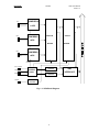
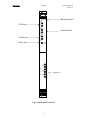
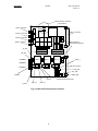
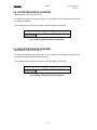
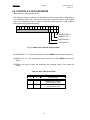
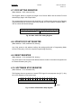
22/07/96
V676 User's Manual
Version 1.2
TABLE OF CONTENTS
TABLE OF CONTENTS ..........................................................................................................i
LIST OF FIGURES .................................................................................................................ii
LIST OF TABLES....................................................................................................................ii
1. DESCRIPTION .................................................................................................................1
1.1. FUNCTIONAL DESCRIPTION.............................................................................1
2. SPECIFICATIONS............................................................................................................4
2.1. EXTERNAL COMPONENTS ...............................................................................4
2.2. INTERNAL COMPONENTS.................................................................................5
2.3. CHARACTERISTICS OF THE SIGNALS.............................................................6
2.4. GENERAL ...........................................................................................................6
2.5. POWER REQUIREMENTS..................................................................................6
3. OPERATING MODES.......................................................................................................10
3.1. GENERAL INFORMATION..................................................................................10
3.2. POWER-ON / RESET STATUS...........................................................................10
3.3. BUFFERING LOGIC............................................................................................11
3.3.1. CIRCULAR BUFFER LENGTH.............................................................11
3.3.2. NUMBER OF SAMPLES TO ACQUIRE ...............................................11
3.3.3. ALMOST EMPTY FLAG.......................................................................12
3.3.4. ALMOST FULL FLAG ..........................................................................12
3.4. PROGRAMMING THE MODULE.........................................................................12
3.5. ACQUISITION SEQUENCE.................................................................................14
3.6. CLOCK OPERATION ..........................................................................................14
3.7. STOP LOGIC ......................................................................................................15
3.8. BUSY LOGIC.......................................................................................................15
3.9. TIME TAG COUNTER .........................................................................................16
4. VME INTERFACE.............................................................................................................17
4.1. ADDRESSING CAPABILITY................................................................................17
4.2. OUTPUT BUFFER REGISTER............................................................................19
4.3. SAMPLE REGISTER...........................................................................................19
4.4. ACCEPTED EVENTS COUNTER........................................................................20
4.5. REJECTED EVENTS COUNTER ........................................................................20
4.6. CONTROL & STATUS REGISTER......................................................................21
4.7. FIFO SETTING REGISTER.................................................................................22
4.8. UPDATE FIFO SET REGISTER ..........................................................................22
4.9. RESET REGISTER .............................................................................................22
4.10. SOFTWARE STOP REGISTER.........................................................................22
APPENDIX A: ELECTRICAL DIAGRAMS ...............................................................................A.1
i
22/07/96
V676 User's Manual
Version 1.2
LIST OF FIGURES
Fig. 1.1: V676 Block Diagram ..................................................................................................3
Fig. 2.1: V676 Front Panel.......................................................................................................7
Fig. 2.2: V676 Components Locations .....................................................................................8
Fig. 2.3: Mod. V676 Jumpers Settings.....................................................................................9
Fig. 3.1: Mod. V676 Buffer Flag Programming Words..............................................................13
Fig. 3.2: Mod. V676 Clock Buffering Scheme ..........................................................................14
Fig. 3.3: Mod. V676 STOP Logic .............................................................................................15
Fig. 4.1: Mod. V676 Base Address Setting ..............................................................................18
Fig. 4.2: Mod. V676 Header Structure .....................................................................................19
Fig. 4.3: Mod. V676 Data Structure .........................................................................................19
Fig. 4.4: Mod. V676 Sample Register ......................................................................................19
Fig. 4.5: Mod. V676 Accepted Events Register........................................................................20
Fig. 4.6: Mod. V676 Rejected Events Register.........................................................................20
Fig. 4.7: Mod. V676 Control & Status Register ........................................................................21
Fig. 4.8: Mod. V676 FIFO Setting Register ..............................................................................22
Fig. 4.9: Mod. V676 Software Stop Register ............................................................................22
LIST OF TABLES
Table 4.1: Address Map for the Mod. V676..............................................................................17
Table 4.2: Mod. V676 Control Bits ...........................................................................................21
ii
22/07/96
V676 User's Manual
Version 1.2
1. DESCRIPTION
1.1. FUNCTIONAL DESCRIPTION
The CAEN Model V676 is a 3 CHANNEL 40 MHz ADC housed in a 1-unit wide VME
module, realized with two independent boards (ADC and FIFO) connected via two 68-pin
connectors (a functional block diagram is shown in Fig. 1.1). The task of this module is to
store in an output buffer a certain number of ADC converted words (10 bit per channel) that
belong to a temporal window placed around a STOP signal.
The module houses three FERMI Analog ASICs (housing a Compressor and an ADC) and
two buffer FIFOs (circular and output, 4K x 32 bits each). At each pulse of the external or
internal CLOCK (40 MHz maximum frequency) the input data are converted and stored in
the circular buffer (30 bit, 10 per channel); when the programmed buffer length is reached,
each oldest datum is lost with the storage of each new input datum.
Each pulse of the External or the Internal CLOCK increments a 30 bit Time Tag Counter.
This Counter is set to 0 by an external CLEAR signal.
At the arrival of an external or software STOP, the data coming from the circular buffer are
transferred to an Output buffer with a Header containing the Time Tag Counter value at the
occurrence of the STOP signal: the User can program via VME the number of samples
before the STOP (i.e. the Circular Buffer length) and the total number of samples to be
transferred in the Output Buffer (length of the temporal window).
The STOP signal also increments an Event Counter whose content is stored in a further
register (12 bit). If the STOP signal occurs during a data transfer from the Circular to the
Output Buffer, or if the Output Buffer is full, the data transfer will not occur and a "Rejected
Event" Counter will be incremented (also available in a 12 bit register).
The status of the module is available on a Status Register for readout via VME.
A front panel LED (DTACK) lights up each time the module generates the VME signal
DTACK. The data contained in the FIFO buffers are accessible via VME either in single
word or in Block Transfer readout.
The Model V676 uses the P1 and P2 connectors of VME.
The module works in A24/A32 mode; the recognized Address Modifier codes are:
AM= %3D
AM= %39
AM= %0D
AM= %09
AM = %3F
AM = %3B
AM = %0F
AM = %0B
standard supervisor data access;
standard user data access;
extended supervisor data access;
extended user data access;
standard supervisor block transfer;
standard user block transfer;
extended supervisor block transfer;
extended user block transfer.
1
22/07/96
V676 User's Manual
Version 1.2
The module's Base Address is fixed by 4 internal rotary switches housed on a piggy-back
board plugged into the main printed circuit boards. The Base Address can be selected in the
range:
%00 0000 <-> %FF 0000
%0000 0000 <-> %FFFF 0000
A24 mode.
A32 mode.
The Registers are accessed in D16 mode; the readout of the Output Buffer is available in
D32 and BLT32 modes only.
(Developed in collaboration with CERN in the frame of the FERMI-RD16 Collaboration)
2
22/07/96
IN 1
V676 User's Manual
Version 1.2
COMPRESS.
+ ADC
IN 2
COMPRESS.
CIRCULAR
OUTPUT
+ ADC
BUFFER
IN 3
BUFFER
COMPRESS.
+ ADC
ADC
CLOCK
EXT. CLOCK
STOP
BUSY
CLEAR
CONTROL
LOGIC
EVENT
COUNTER
REJECT. EVENT
COUNTER
TIME TAG
COUNTER
Fig. 1.1: V676 Block Diagram
3
VME
INTERFACE
22/07/96
V676 User's Manual
Version 1.2
2. SPECIFICATIONS
2.1. EXTERNAL COMPONENTS
(Refer to Fig. 2.1)
CONNECTORS
- N. 2, "STOP", input connectors, LEMO 00 type; two bridged connectors (for daisy
chaining) for the STOP signal.
- N. 2, "CLK", input connectors, LEMO 00 type; two bridged connectors (for daisy chaining)
for the external CLOCK signal.
- N. 2, "CLR", input connectors, LEMO 00 type; two bridged connectors (for daisy chaining)
for the external CLEAR signal.
- N. 1, "BUSY", output connector, LEMO 00 type, for the BUSY signal.
- N. 6, "CH1..CH3 +/-", input connectors, SMC R112305 type. Connectors for the INPUT
signals.
DISPLAYS
- N. 1, "DTACK", green LED, VME selected; it lights up during a VME access.
- N. 1, "BUSY", red LED; it lights up when the module is Busy.
4
22/07/96
V676 User's Manual
Version 1.2
2.2. INTERNAL COMPONENTS
(Refer to Fig. 2.2)
CONNECTORS
- N. 4, connectors, 2*D3467 and 2*D3567 Type (CERN SCEM 09.55.21.368.0 and
09.55.21.568.4). Connectors for the FIFO and ADC boards connection.
SWITCHES, JUMPERS
(Refer to Fig. 2.2, 2.3)
N. 4, rotary switches for the module's VME Base Address selection.
N. 1, "S0", DIP switch, for the External / Internal (EXT/INT) Clock selection.
N. 2, "S1", DIP switches, to insert a division by 2 (DIV2) of the CLOCK frequency for each
inserted DIP switch (both inserted = CLOCK/4: Clock is divided by 4).
•
•
•
•
+12V JMP
-12V JMP
AGND JMP
CENT_J
Jumper inserted, connects the analog part to the +12V power supply;
Jumper inserted, connects the analog part to the -12V power supply;
Jumper inserted, connects the analog ground to the digital ground;
Jumper must be inserted in the left position;
(in the following, only one representative for channel 1 is mentioned; channel 2 and 3
jumpers are numbered accordingly, e.g., JM_ADIN2 or JM_ADIN3 )
•
•
•
•
•
•
•
•
JM_ADIN1
Connects the ADC +input to a signal source, either the level shifter
output (the upper location) or directly to the input connector for using only the ADC and
not the compressor and level shifter (the lower location);
JG_ADIN1
Connects the ADC -input to either the AGND (the upper location, for
using the ADC only) or to the base line control circuitry (the lower location, for using the
compressor and the level shifter);
+JMP_C1 Single ended (right position) or differential (left) selection;
-JMP_C1 Single ended (right position) or differential (left) selection;
+J_INC1 Negative (left location) or positive (right location) going signal when using the
compressor in single ended mode;
-J_INC1 Positive (left location) or negative (right location) going signal when using the
compressor in single ended mode;
J_10.5V1 Connects the +10.5V power for the compressor to the internal (upper
position) or external (lower position) power supply. To be set in the lower position;
STR100 Positive input signal routing. Up for ADC directly, left for single ended, and
right for differential input signal.
5
22/07/96
V676 User's Manual
Version 1.2
2.3. CHARACTERISTICS OF THE SIGNALS
INPUTS:
- ANALOG INPUTS: With compressor inserted:
2 V single ended, positive or negative pulses
(selection via internal jumpers, see Fig. 2.3);
± 2 V differential; 50 Ω impedance (referred to ground).
Without compressor inserted:
2 V single ended, positive pulses
(selection via internal jumpers, see Fig. 2.3);
50 Ω impedance (referred to ground);
- STOP:
Std. NIM level, high impedance (1 kΩ); input bridged connectors.
Min. width: 1 Divided Clock cycle (i.e. at the frequency on the output
of the Clock Division stage, see Fig. 3.2).
Min. time between 2 STOP pulses: 4 Divided Clock cycles
(i.e. at the frequency on the output of the Clock Division stage).
- CLOCK:
Std. NIM level, high impedance (1 kΩ); input bridged connectors.
Maximum frequency: 40 MHz; Duty cycle: 50%.
- CLEAR:
Std. NIM level, high impedance (1 kΩ); input bridged connectors.
Min. width: 1 Divided Clock cycle (i.e. at the frequency on the output
of the Clock Division stage, see Fig. 3.2).
OUTPUTS:
- BUSY:
Std. NIM level on 50 Ω impedance
2.4. GENERAL
- RESOLUTION:
- DYNAMIC RANGE:
- INPUT SENSITIVITY:
10 bits;
15 bits (with compressor inserted);
100 µV/count at low input amplitude (compressor inserted);
2 mV/count (without compressor).
- DIFFERENTIAL NONLINEARITY (ADC ONLY):
< ±0.5 LSB;
- INTEGRAL NONLINEARITY (ADC ONLY): < ±1 LSB;
- ANALOG BANDWIDTH:
20 MHz.
2.5. POWER REQUIREMENTS
+ 12 V
− 12 V
+5V
0.5 A
0.3 A
1.5 A
6
22/07/96
V676 User's Manual
Version 1.2
Mod. V560E
Mod. V676
VME selected LED
DTACK
STOP input
S
T
O
P
C
L
K
CLEAR input
BUSY output
External CLOCK
C
L
R
B
U
S
Y
CH3
I +
N P CH2
U +
T S CH1
+
Inputs 1..3
3 CH 10 BIT
40 MHz ADC
Fig. 2.1: Mod. V676 Front Panel
7
22/07/96
V676 User's Manual
Version 1.2
CLOCK Selection & Division
DIP Switches
EXT
STOP connectors
DIV2
DIV2
S0
INT
S1
VME P1 connector
CLOCK connectors
CLEAR connectors
BUSY connector
Rotary switches
for Base address selection
JG_AD1
JM_AD1
CHANNEL3 +
+
CHANNEL2
+
CHANNEL1
-
ADC 1
ADC 2
CENT_J
ADC 3
VME P2 connector
+12V_JMP
-12V_JMP
AGND_JMP
STR100
+J_INC1
J_10.5V1
-J_INC1
-JMP_C1
Component side of the board
+JMP_C1
Fig. 2.2: Mod. V676 Components Locations
8
22/07/96
POT 5
V676 User's Manual
Version 1.2
+IN_AD
down
-IN_AD
ADC
OUT_AD
up
JG_ADIN1
LS_OUT
+IN
LEVEL
SHIFTER
LS_IN
LS_OFFS
STR100
up
FEEDBACK
AMPLIFIER
down up
right
left
+
left
right
right
JM_ADIN1
FA_OUT
-FA_IN
+FA_IN
left
+JMP_C1
+J_INC1
+IN_C
-IN
-
-JMP_C1
right
left
right
-IN_C
left
POT 51
COMPRESSOR
-J_INC1
down
up
VR_OUT
OUT_C
+10.5V_C
VOLTAGE
REGULATOR
J_10.5V
Single ended with no compressor:
STR100
up
JM_ADIN1
down
JG_ADIN1
up
Single ended with compressor:
STR100
left
JM_ADIN1
up
JG_ADIN1
down
+JMP_C1
right
-JMP_C1
right
Single ended with compressor
configuration options:
Positive signals:
+J_INC1
right
-J_INC1
left
Negative signals:
+J_INC1
left
-J_INC1
right
Differential with compressor:
STR100
right
JM_ADIN1
up
JG_ADIN1
down
+JMP_C1
left
-JMP_C1
left
Fig. 2.3: Mod. V676 Jumpers Settings
9
SERVO
LOOP
22/07/96
V676 User's Manual
Version 1.2
3. OPERATING MODES
3.1. GENERAL INFORMATION
The CAEN Model V676 is a 3 CHANNEL 40 MHz ADC housed in a 1-unit wide VME
module. The task of this module is to store in an output buffer a certain number of ADC
converted words (10 bit per channel) that belong to a temporal window placed around a
STOP signal.
The module houses three FERMI Analog ASICs (housing a Compressor and an ADC) and
two buffer FIFOs (circular and output, 4K x 32 bits each). At each pulse of the external or
internal CLOCK (40 MHz maximum frequency) the input data are converted and stored in
the circular buffer (30 bit, 10 per channel); when the programmed buffer length is reached,
each oldest datum is lost with the storage of each new input datum.
Each pulse of the External or the Internal Divided CLOCK (see §3.6) increments a 30 bit
Time Tag Counter. This Counter is set to 0 by an external CLEAR signal.
At the arrival of an external or software STOP , the data coming from the circular buffer are
transferred to an Output buffer with a Header containing the Time Tag Counter value: the
User can program via VME the number of samples before the STOP (i.e. the Circular Buffer
length) and the total number of samples to be transferred in the Output Buffer (length of the
temporal window).
The STOP signal also increments an Event Counter whose content is stored in a further
register (12 bit). If the STOP signal occurs during a data transfer from the Circular to the
Output Buffer, or if the Output Buffer is full, the data transfer will not occur and a "Rejected
Event" Counter will be incremented (also available in a 12 bit register).
The status of the module is available on a Status Register for readout via VME.
3.2. POWER-ON / RESET STATUS
At Power-ON, the module is in the following status:
1.
2.
3.
4.
5.
6.
the Time Tag Counter is set to 0 (see § 4.2);
the Accepted Events Counter is set to 0 (see § 4.4);
the Rejected Events Counter is set to 0 (see § 4.5);
the Sample Register is set to 1024 (see § 4.3);
the Circular and the Output Buffers are cleared;
the module is set to Buffers Programming mode (see § 4.6).
The VME Reset (access to address Base + %10) and the generation of the VME signal
SYSRES perform the same actions.
At Power-ON or after a reset the Buffers must thus be initialized (see § 3.3).
10
22/07/96
V676 User's Manual
Version 1.2
3.3. BUFFERING LOGIC
The User can program via VME the number of samples before the STOP (i.e. the Circular
Buffer length), the total number of samples to be transferred in the Output Buffer (length of
the temporal window) and two flags (Almost Empty, Almost Full) that allow to manage the
data flow to and from the Output Buffer.
Here below is described the logic of this buffering scheme for each programmable variable
with some suggested operations for a correct setting.
3.3.1. CIRCULAR BUFFER LENGTH
When the module is in acquisition mode it converts and stores in the Circular Buffer the
incoming input signals. Once a STOP signal occurs, the Circular Buffer will already contain
a certain number of samples that the User may wish to acquire (data before the STOP). The
Circular Buffer length must thus be set taking into account that both the FERMI ADC and
the internal Stop Processor Logic introduce a certain number of Clock cycles of latency.
The overall effect of the above is that if the User wants to acquire m samples before the
occurrence of the STOP He/She must set a Circular Buffer Length (CBL) that is.
CBL = BUFLENGTH + 12 - m
where BUFLENGTH is the size of the FIFOs used in the module (4096) and m must satisfy
the relation:
13 ≤ m ≤ BUFLENGTH + 12.
3.3.2. NUMBER OF SAMPLES TO ACQUIRE
The total number of samples to acquire must be the sum of the m samples already present
in the Circular Buffer and the l samples after the STOP signal that the User wishes to
acquire. The total number n to be written in the Sample Register (see § 4.3) is thus:
n = m + l.
When the content of the Circular Buffer (m samples already present + l newly incoming
samples) is transferred to the Output Buffer, a Header is written in the Output Buffer, so the
total number of words present in the Output Buffer will be n+1 for each event.
11
22/07/96
V676 User's Manual
Version 1.2
3.3.3. ALMOST EMPTY FLAG
The Output Buffer Almost Empty (OBAE) is a number that can be set from 0 to 4095. The
relevant flag (/AE, see 4.6) indicates, when set to 1, that the Output Buffer has at least a
number OBAE+1 of words to be read out. This information can be useful both in single
readout or in Block Transfer readout modes:
a) for single readout, the User could, e.g., set OBAE equal to the block length (OBAE = n),
trigger the acquisition on the /Almost Empty bit in the Control & Status Register (see § 4.6)
and perform a readout of the n+1 words.
b) for Block Transfer cycles, the User could set
OBAE = p*(BLT_LENGTH) -1
where BLT_LENGTH is the Block Transfer length (e.g. 256 byte = 64 words), trigger the
acquisition on the /Almost Empty bit in the Control & Status Register (see § 4.6) and
perform p Block Transfer cycles.
The /FIFO Empty bit available in the data (bit 30, see § 4.2) represents the status of the
Output Buffer AFTER the current readout, i.e. after readout of the word that contains the
/FIFO Empty bit itself. It is suggested NOT to use this bit to trigger the readout of the Output
Buffer: this bit should be used only for diagnostic purposes.
3.3.4. ALMOST FULL FLAG
The Output Buffer Almost Full (OBAF) is a number that can be set from 1 to 4095. The
relevant flag (/AF, see 4.6) indicates, when set to 1, that the Output Buffer has still sufficient
space to store at least a number OBAF+1 of words. This flag is used by the Control Logic to
enter the BUSY state. The value of OBAF can be set taking into account the following:
1. the User can limit the Output Buffer length;
2. if the User wants to use all the Output Buffer length, care must be taken NOT to break
up an event: if OBAF is set to n, with n = total number of samples to acquire (see
§ 3.3.2), a whole event will fit in the reserved space of the Output Buffer and thus no
data will be lost.
3.4. PROGRAMMING THE MODULE
The User can program via VME the number of samples before the STOP (i.e. the Circular
Buffer length), the total number of samples to be transferred in the Output Buffer (length of
the temporal window) and two flags (Almost Empty, Almost Full) that allow to manage the
data flow to and from the Output Buffer as described above in §3.3.
The Circular Buffer Length is set as a 12 bit word containing the desired length split in 2
parts (respectively 8 and 4 bits each) written in the FIFO Set Registes in 2 following
accesses (confirming each time the set value via the Update FIFO Set Register).
The Almost Full and Almost Empty Flags in the Output Buffer are set as 12 bit words
containing the desired Flag position split in 2 parts (respectively 8 and 4 bits each) written in
12
22/07/96
V676 User's Manual
Version 1.2
the FIFO Set Register in 2 following accesses (confirming each time the set value via the
Update FIFO Set Register).
15 14 13 12 11 10 9
WORD 1
WORD 2
WORD 3
WORD 4
8
7
6
5
4
3
2
1
0
OBAE[7..0]
OBAE[11..8]
OBAF[7..0]
CBL[7..0]
OBAF[11..8]
CBL[11..8]
OBAE = OUTPUT BUFFER ALMOST EMPTY FLAG
OBAF = OUTPUT BUFFER ALMOST FULL FLAG
CBL = CIRCULAR BUFFER LENGTH
Fig. 3.1: Mod. V676 Buffer Flag Programming Words
In order to program the Module, either at Power-ON or for a change in the settings, the User
must perform the following actions:
1. Perform a Reset (access to address Base + %10) or a VME SYSRES;
2. Write in the FIFO Setting Register (address Base + %0C) a word containing in the 8
uppermost bits (bits 8 to 15) the 8 lowermost bits (bits 0 to 7) of the Almost Empty Flag
in the Output Buffer (see WORD 1 in Fig. 3.1);
3. Perform an access to the Update FIFO Set Register (address Base + %0E);
4. Write in the FIFO Setting Register (address Base + %0C) a word containing in the bits 8
to 11 the 4 uppermost bits (bits 8 to 11) of the Almost Empty Flag in the Output Buffer
(see WORD 2 in Fig. 3.1);
5. Perform an access to the Update FIFO Set Register (address Base + %0E);
6. Write in the FIFO Setting Register (address Base + %0C) a word containing in the 8
uppermost bits (bits 8 to 15) the 8 lowermost bits (bits 0 to 7) of the Almost Full Flag in
the Output Buffer and in the 8 lowermost bits (bits 0 to 7) the 8 lowermost bits (bits 0 to
7) of the Circular Buffer Length (see WORD 3 in Fig. 3.1);
7. Perform an access to the Update FIFO Set Register (address Base + %0E);
8. Write in the FIFO Setting Register (address Base + %0C) a word containing in the bits 8
to 11 the 4 uppermost bits (bits 8 to 11) of the Almost Full Flag in the Output Buffer and
in the bits 0 to 3 the 4 uppermost bits (bits 8 to 11) of the Circular Buffer Length (see
WORD 4 in Fig. 3.1);
9. Perform an access to the Update FIFO Set Register (address Base + %0E);
10. Write in the Samples Register (address Base + %04) a 12 bit word that contains the
desired Number of Samples to be transferred from the Circular Buffer to the Output
Buffer for a given STOP signal (allowed values 1 to 4095, see also § 4.3);
11. Set the Module to Acquisition Mode via the Control & Status Register (see § 4.6).
During all points of the above sequence of operations, the Module is in Busy status. Any
STOP signal occurring does NOT increment the Rejected Events Counter.
This sequence of operations must be performed at Power-ON and each time the module
must be re-programmed.
13
22/07/96
V676 User's Manual
Version 1.2
3.5. ACQUISITION SEQUENCE
When the module is switched back to the Acquisition Mode, it is ready to accept a STOP
signal. In order to have correct timings, the User may wish to clear the Time Tag Counter
with a CLEAR pulse in the relevant Front Panel connectors.
If the module is not BUSY, the leading edge of a pulse on the STOP input, synchronized
with the Divided Clock cycle, starts the Control Logic, that performs the following operations:
•
sets the module in the BUSY condition;
•
starts the transfer of the selected number of samples in the Output Buffer;
•
increments the Accepted Events Counter;
A suggested readout scheme may involve the use of the /Almost Empty bit in the Control &
Status Register:
•
•
wait until the /Almost Empty bit in the Control & Status Register is set to 1;
read out from the Output Buffer N words, with N ≤ OBAE+1 (see § 3.3.3)
3.6. CLOCK OPERATION
A DIP switch (S0) placed on the Printed Circuit Board (see Fig. 2.2) allows to select the
CLOCK as being External (switch on EXT) or Internal (switch on INT).
The selected CLOCK is then fed to a Clock Division stage. Two DIP switches (S1) placed
on the Printed Circuit Board (see Fig. 2.2) allow to insert a division by two of the Clock
frequency. Each DIP switch inserts a division by 2. When both switches are inserted, the
CLOCK frequency is divided by 4, if none is inserted the Clock frequency is unaltered. In
particular, with the Internal CLOCK the User can obtain 40 MHz, 20 MHz and 10 MHz
sample rates. Moreover, each divided Clock cycle will increment the Time Tag Counter.
The external clock (CLK input), must be a NIM signal on 50 Ω.
The clock selection scheme is shown in the following figure.
EXTERNAL
CLOCK
EXT
INT
CLOCK
DIVIDER
40 MHz
INTERNAL
CLOCK
DIV2
DIV2
Fig. 3.2: Mod. V676 Clock Buffering Scheme
14
DIVIDED
CLOCK
22/07/96
V676 User's Manual
Version 1.2
3.7. STOP LOGIC
The Stop Processor is synchronized with the Divided Clock. Due to this, the sampled
waveform will have a jitter of ±½ Divided Clock cycle with respect to the STOP signal.
The STOP can be either an external signal or an internal level generated by setting the first
bit of the STOP Register (see § 4.10). Once set the bit in the STOP Register and after one
Divided Clock cycle, the first bit of the STOP Register MUST be set back to 0.
STOP
SYNC
STOP
REGISTER
STOP
PROCESSOR
TO BUFFERS
ACQ MODE ON
DIVIDED
CLOCK
Fig. 3.3: Mod. V676 STOP Logic
3.8. BUSY LOGIC
The module can enter a BUSY status for any of the following reasons:
1. a data transfer is taking place during an ordinary acquisition from the Circular Buffer to
the Output Buffer;
2. the Output Buffer is Almost Full (bit 1 of Control & Status Register set to 0, see § 4.6);
3. the module is NOT in Acquitision Mode (see § 4.6).
When the module is BUSY it does not accept any STOP signals. If the BUSY status is due
to point 1. or 2. above, the STOP signal will increment the Rejected Events Counter (see §
4.5).
If the BUSY status is due to point 3. above (i.e., the module is either in Programming Mode
or in CAEN Internal Test), any STOP signal occurring does NOT increment the Rejected
Events Counter.
15
22/07/96
V676 User's Manual
Version 1.2
3.9. TIME TAG COUNTER
Each pulse of the External or the Internal Divided CLOCK (SEE §3.6) increments a 30 bit
Time Tag Counter. This Counter is set to 0 by an external CLEAR signal. The CLEAR must
be a Std. NIM level: when present, its action is to hold to 0 the Counter and start it once
released. The CLEAR is synchronized with the Divided Clock. Due to this, the occurrence
of the physical Clear of the Time Tag Counter will have a jitter of 1 Divided Clock cycle with
respect to the input CLEAR signal.
The Header that is written in the Output Buffer represents the absolute arrival time of the
STOP signal with respect to the CLEAR release. In order to obtain the actual absolute time
measurement of the arrival of the STOP signal, the User must use the following formula:
Tabs = (TIME_TAG - 3)*DIV_CLOCK
where Tabs is the absolute time, TIME_TAG is the Header value and DIV_CLOCK is the
divided clock period. E.g., if the Header contains a value of 2500 and the Internal CLOCK is
used with a DIV2 switch inserted (20 MHz sampling rate), the absolute time is
Tabs = (2500 - 3)*50 ns = 124850 ns.
16
22/07/96
V676 User's Manual
Version 1.2
4. VME INTERFACE
4.1. ADDRESSING CAPABILITY
The V676 module works in A24/A32, D16/D32 mode. This implies that the module's address
must be specified in a field of 24 or 32 bits. The Address Modifiers codes recognized by the
module are:
AM=%3F:
AM=%3D:
AM=%3B:
AM=%39:
AM=%0F:
AM=%0D:
AM=%0B:
AM=%09:
A24 supervisory block transfer (BLT)
A24 supervisory data access
A24 user block transfer (BLT)
A24 user data access
A32 supervisory block transfer (BLT)
A32 supervisory data access
A32 user block transfer (BLT)
A32 user data access
The module's Base Address is fixed by 4 internal rotary switches housed on two piggy-back
boards plugged into the main printed circuit board.
The Base Address can be selected in the range:
% 00 0000 <-> % FF 0000
% 0000 0000 <-> % FFFF 0000
A24 mode
A32 mode
The Address Map of the page is shown in Table 4.1.
Table 4.1: Address Map for the Mod. V676
ADDRESS
REGISTER/CONTENT
Base + %FFFE
.
.
Base + %14
Not used
.
.
Not used
Base + %12
Base + %10
Base + %0E
Base + %0C
Base + %0A
Base + %08
Base + %06
Base + %04
Base + %00
Software STOP Register
Reset Register
Update FIFO Set Register
FIFO Setting Register
Control & Status Register
Rejected Events Counter
Accepted Events Counter
Sample Register
Output Buffer Register
17
TYPE
read/write D16
read/write D16
read/write D16
write only D16
read/write D16
read only D16
read only D16
read/write D16
read only D32/BLT32
22/07/96
Base address bit <23..20>
Base address bit <19..16>
Base address bit <31..28>
Component side of the board
Base address bit <27..24>
Fig. 4.1: Mod. V676 Base Address Setting
18
V676 User's Manual
Version 1.2
22/07/96
V676 User's Manual
Version 1.2
4.2. OUTPUT BUFFER REGISTER
(Base Address + %0, read only D32/BLT32)
This location allows to readout the data stored in the output Buffer. The structure of the
Header is shown in Fig. 4.2. Its content is explained in §3.9.
31 30 29 28 27 26 25 24 23 22 21 20 19 18 17 16 15 14 13 12 11 10 9 8 7 6 5 4 3 2 1 0
1
TIME TAG COUNTER
/E
/ FIFO EMPTY
HEADER IDENTIFIER
Fig. 4.2: Mod. V676 Header Structure
/FIFO EMPTY
1= Output Buffer Not Empty
0= Output Buffer Empty
The structure of the Data is shown in Fig. 4.3.
31 30 29 28 27 26 25 24 23 22 21 20 19 18 17 16 15 14 13 12 11 10 9 8 7 6 5 4 3 2 1 0
0
/E
SAMPLE ADC 2
SAMPLE ADC 1
SAMPLE ADC 0
/ FIFO EMPTY
DATA IDENTIFIER
Fig. 4.3: Mod. V676 Data Structure
N.B.: The Sample ADC Data are stored in the Output Buffer with
inverted bits: in order to obtain the actual converted value, the User
must invert the bits' values for each bit.
4.3. SAMPLE REGISTER
(Base Address + %04, read/write D16)
It contains the number of samples that are transferred from the Circular Buffer to the Output
Buffer for a given STOP signal. Allowed values: up to 4095.
15 14 13 12 11 10 9
8
7
6
5
4
3
NUMBER OF SAMPLES
Fig. 4.4: Mod. V676 Sample Register
19
2
1
0
22/07/96
V676 User's Manual
Version 1.2
4.4. ACCEPTED EVENTS COUNTER
(Base Address + %06, read only D16)
It contains the number of accepted events, i.e. the number of STOP signals occurred while
the module is not Busy.
This Register must be read out only when no STOP signals are occurring.
15 14 13 12 11 10 9
8
7
6
5
4
3
2
1
0
NUMBER OF ACCEPTED EVENTS
Fig. 4.5: Mod. V676 Accepted Events Register
4.5. REJECTED EVENTS COUNTER
(Base Address + %08, read only D16)
It contains the number of rejected events, i.e. the number of STOP signals occurred while
the module is Busy during the Acquisition Mode.
This Register must be read out only when no STOP signals are occurring.
15 14 13 12 11 10 9
8
7
6
5
4
3
2
1
NUMBER OF REJECTED EVENTS
Fig. 4.6: Mod. V676 Rejected Events Register
20
0
22/07/96
V676 User's Manual
Version 1.2
4.6. CONTROL & STATUS REGISTER
(Base Address + %0A, read/write D16)
This Register contains 2 read/write bits that allow to set the module either in Programming
or in Acquisition Mode, and 2 read only bits that allow to monitorthe status of the Output
Buffer. The Control bits are set to 1 after an access to the Reset Register, a VME SYSRES
and at Power-ON (Programming mode).
15 14 13 12 11 10 9
8
7
6
5
4
3
2
1
0
CB1 CB0 /AF /AE
/ ALMOST EMPTY
/ ALMOST FULL
CONTROL BIT 0
CONTROL BIT 1
Fig. 4.7: Mod. V676 Control & Status Register
/ALMOST EMPTY: if = 1 the Output Buffer has at least OBAE+1 stored words (see §3.3.3).
/ALMOST FULL: if = 1 the Output Buffer has at least room for other OBAF+1 words (see
§3.3.4).
CONTROL: the status of these bits determines the operating mode of the module as
follows.
Table 4.2: Mod. V676 Control Bits
CB0
0
1
1
CB1
0
1
0
0
1
MODE
ACQUISITION
BUFFERS PROGRAMMING
CAEN Internal Test Only
(not allowed to User)
CAEN Internal Test Only
(not allowed to User)
21
22/07/96
V676 User's Manual
Version 1.2
4.7. FIFO SETTING REGISTER
(Base Address + %0C, write only D16)
This Register allows to program the length of the Circular Buffer and the Almost Full and
Almost Empty flags in the Output Buffer.
The programming sequences are fully described in § 3.4. Each write access to this Register
must be followed by an access to the dummy Update FIFO Set Register at address Base +
%0E to activate the desired settings.
15 14 13 12 11 10 9
8
7
OUTPUT BUFFER SETTINGS
6
5
4
3
2
1
0
CIRCULAR BUFFER SETTINGS
Fig. 4.8: Mod. V676 FIFO Setting Register
4.8. UPDATE FIFO SET REGISTER
(Base Address + %0E, read/write D16, dummy)
Any 16-bit access to this address confirms the settings performed in Programming Mode
into the FIFOs (see § 3.4 for the complete Programming sequence).
4.9. RESET REGISTER
(Base Address + %10, read/write D16, dummy)
Any 16-bit read or write access to this address sets the module in the same configuration as
the Power-ON status (see § 3.2).
4.10. SOFTWARE STOP REGISTER
(Base Address + %12, read/write D16)
This Register allows to generate an internal STOP signal for test purposes (see § 3.7). Only
bit 0 of this Register is used (active high).
15 14 13 12 11 10 9
8
7
6
5
4
3
2
1
0
STOP
Fig. 4.9: Mod. V676 Software Stop Register
22
22/07/96
APPENDIX A: ELECTRICAL DIAGRAMS
A.1
V676 User's Manual
Version 1.2