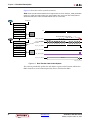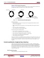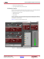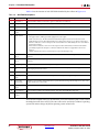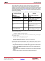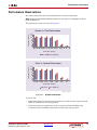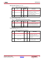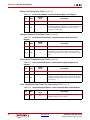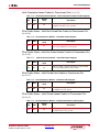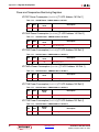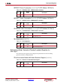
1
AC701 Base Targeted
Reference Design
(Vivado Design Suite 2014.3)
User Guide
UG964 (v5.0) December 18, 2014
Notice of Disclaimer
The information disclosed to you hereunder (the “Materials”) is provided solely for the selection and use of Xilinx products. To the maximum
extent permitted by applicable law: (1) Materials are made available "AS IS" and with all faults, Xilinx hereby DISCLAIMS ALL
WARRANTIES AND CONDITIONS, EXPRESS, IMPLIED, OR STATUTORY, INCLUDING BUT NOT LIMITED TO WARRANTIES OF
MERCHANTABILITY, NON-INFRINGEMENT, OR FITNESS FOR ANY PARTICULAR PURPOSE; and (2) Xilinx shall not be liable (whether
in contract or tort, including negligence, or under any other theory of liability) for any loss or damage of any kind or nature related to, arising
under, or in connection with, the Materials (including your use of the Materials), including for any direct, indirect, special, incidental, or
consequential loss or damage (including loss of data, profits, goodwill, or any type of loss or damage suffered as a result of any action
brought by a third party) even if such damage or loss was reasonably foreseeable or Xilinx had been advised of the possibility of the same.
Xilinx assumes no obligation to correct any errors contained in the Materials or to notify you of updates to the Materials or to product
specifications. You may not reproduce, modify, distribute, or publicly display the Materials without prior written consent. Certain products are
subject to the terms and conditions of the Limited Warranties which can be viewed at http://www.xilinx.com/warranty.htm; IP cores may be
subject to warranty and support terms contained in a license issued to you by Xilinx. Xilinx products are not designed or intended to be
fail-safe or for use in any application requiring fail-safe performance; you assume sole risk and liability for use of Xilinx products in Critical
Applications: http://www.xilinx.com/warranty.htm#critapps.
Automotive Applications Disclaimer
XILINX PRODUCTS ARE NOT DESIGNED OR INTENDED TO BE FAIL-SAFE, OR FOR USE IN ANY APPLICATION REQUIRING
FAIL-SAFE PERFORMANCE, SUCH AS APPLICATIONS RELATED TO: (I) THE DEPLOYMENT OF AIRBAGS, (II) CONTROL OF A
VEHICLE, UNLESS THERE IS A FAIL-SAFE OR REDUNDANCY FEATURE (WHICH DOES NOT INCLUDE USE OF SOFTWARE IN THE
XILINX DEVICE TO IMPLEMENT THE REDUNDANCY) AND A WARNING SIGNAL UPON FAILURE TO THE OPERATOR, OR (III) USES
THAT COULD LEAD TO DEATH OR PERSONAL INJURY. CUSTOMER ASSUMES THE SOLE RISK AND LIABILITY OF ANY USE OF
XILINX PRODUCTS IN SUCH APPLICATIONS.
Fedora Information
Xilinx obtained the Fedora Linux software from Fedora (http://fedoraproject.org/), and you may too. Xilinx made no changes to the software
obtained from Fedora. If you desire to use Fedora Linux software in your product, Xilinx encourages you to obtain Fedora Linux software
directly from Fedora (http://fedoraproject.org/), even though we are providing to you a copy of the corresponding source code as provided
to us by Fedora. Portions of the Fedora software may be covered by the GNU General Public license as well as many other applicable open
source licenses. Please review the source code in detail for further information. To the maximum extent permitted by applicable law and if
not prohibited by any such third-party licenses, (1) XILINX DISCLAIMS ANY AND ALL EXPRESS OR IMPLIED WARRANTIES,
INCLUDING, BUT NOT LIMITED TO, THE IMPLIED WARRANTIES OF MERCHANTABILITY AND FITNESS FOR A PARTICULAR
PURPOSE; AND (2) IN NO EVENT SHALL XILINX BE LIABLE FOR ANY DIRECT, INDIRECT, INCIDENTAL, SPECIAL, EXEMPLARY, OR
CONSEQUENTIAL DAMAGES (INCLUDING, BUT NOT LIMITED TO, PROCUREMENT OF SUBSTITUTE GOODS OR SERVICES; LOSS
OF USE,DATA, OR PROFITS; OR BUSINESS INTERRUPTION) HOWEVER CAUSED AND ON ANY THEORY OF LIABILITY, WHETHER
IN CONTRACT, STRICT LIABILITY, OR TORT (INCLUDING NEGLIGENCE OR OTHERWISE) ARISING IN ANY WAY OUT OF THE USE
OF THIS SOFTWARE, EVEN IF ADVISED OF THE POSSIBILITY OF SUCH DAMAGE.
Fedora software and technical information is subject to the U.S. Export Administration Regulations and other U.S. and foreign law, and may
not be exported or re-exported to certain countries (currently Cuba, Iran, Iraq, North Korea, Sudan, and Syria) or to persons or entities
prohibited from receiving U.S. exports (including those (a) on the Bureau of Industry and Security Denied Parties List or Entity List, (b) on
the Office of Foreign Assets Control list of Specially Designated Nationals and Blocked Persons, and (c) involved with missile technology or
nuclear, chemical or biological weapons). You may not download Fedora software or technical information if you are located in one of these
countries, or otherwise affected by these restrictions. You may not provide Fedora software or technical information to individuals or entities
located in one of these countries or otherwise affected by these restrictions. You are also responsible for compliance with foreign law
requirements applicable to the import and use of Fedora software and technical information.
© Copyright 2012–2014 Xilinx, Inc. Xilinx, the Xilinx logo, Artix, ISE, Kintex, Spartan, Virtex, Vivado, Zynq, and other designated brands
included herein are trademarks of Xilinx in the United States and other countries. All other trademarks are the property of their respective
owners.
AC701 Base TRD User Guide
www.xilinx.com
UG964 (v5.0) December 18, 2014
Revision History
The following table shows the revision history for this document.
Date
Version
Revision
12/24/2012
1.0
Initial Xilinx release.
04/16/2013
2.0
Added note to Chapter 1, Introduction and to Simulation Requirements. Replaced
references to Modelsim simulator with QuestaSim throughout. Added Table 2-3.
Updated Linux Driver Installation, Overview, and User-Controlled Macros. Added
Simulation Using QuestaSim and Simulation Using the Vivado Simulator. Updated
paragraph after Table 2-6. Replaced references to UG477, 7 Series FPGAs Integrated Block
for PCI Express User Guide, with PG054, 7 Series FPGAs Integrated Block for PCI Express
Product Guide throughout.
11/22/2013
3.0
Updated version references for Vivado Design Suite from 2013.2 to 2013.3. Added
caution note about power connections to J49 on the AC701 board on page 14. Corrected
the LED Status and Notes for pin 2 and pin 3 in Table 2-3, page 15. Updated Chapter 2
sections Implementing the Design Using Vivado HDL Flow, page 23, Reprogramming
the AC701 Board, page 24, Simulation Using QuestaSim, page 26, Simulation Using the
Vivado Simulator, page 27, User-Controlled Macros, page 27, and Test Selection,
page 28. Updated Chapter 5 Descriptor Ring Size, page 59, and Driver Mode of
Operation, page 60. Revised Appendix B, Directory Structure, including Figure B-1,
page 75 and descriptions of directory structure. Revised all links and references in
Appendix E, Additional Resources and revised links to web pages and documents
throughout document to conform to latest style convention.
01/17/2014
4.0
Updated version references for Vivado Design Suite from 2013.3 to 2013.4. Added
Implementing the Design Using Vivado IP Integrator Flow, page 23. Added
IP_Package folder to Figure B-1 and summary description of the IP_Package folder
Hardware Folder, page 75 contents. Revised file name from a7_base_trd_gui.tcl to
a7_base_trd_gui_rtl.tcl in two places on page 23, one place on page 27, and one
place on page 28.
07/03/2014
4.1
Changed all instances of Vivado GUI to Vivado IDE. Revised the procedures under
Implementing the Design Using Vivado HDL Flow, page 23, and Implementing the
Design Using Vivado IP Integrator Flow, page 23. Revised Figure 2-14, page 24 by
moving the control computer USB cable connection from the AC701 board connector J17
to the Digilent mini-B connector.
12/18/2014
5.0
Updated version references for Vivado Design Suite from 2014.1 to 2014.3. Updated
resource utilization values in Table 1-1. Updated the directory where BIT and MCS files
are located from configure_ac701 to ready_to_test on page 22.
UG964 (v5.0) December 18, 2014
www.xilinx.com
AC701 Base TRD User Guide
AC701 Base TRD User Guide
www.xilinx.com
UG964 (v5.0) December 18, 2014
Table of Contents
Revision History . . . . . . . . . . . . . . . . . . . . . . . . . . . . . . . . . . . . . . . . . . . . . . . . . . . . . . . . . . . . . 3
Chapter 1: Introduction
Base TRD Features . . . . . . . . . . . . . . . . . . . . . . . . . . . . . . . . . . . . . . . . . . . . . . . . . . . . . . . . . . . 8
Application Features . . . . . . . . . . . . . . . . . . . . . . . . . . . . . . . . . . . . . . . . . . . . . . . . . . . . . . . . . 9
Resource Utilization. . . . . . . . . . . . . . . . . . . . . . . . . . . . . . . . . . . . . . . . . . . . . . . . . . . . . . . . . . 9
Chapter 2: Getting Started
Requirements . . . . . . . . . . . . . . . . . . . . . . . . . . . . . . . . . . . . . . . . . . . . . . . . . . . . . . . . . . . . . . .
Hardware Demonstration Setup . . . . . . . . . . . . . . . . . . . . . . . . . . . . . . . . . . . . . . . . . . . . .
Rebuilding the Design . . . . . . . . . . . . . . . . . . . . . . . . . . . . . . . . . . . . . . . . . . . . . . . . . . . . . .
Simulation . . . . . . . . . . . . . . . . . . . . . . . . . . . . . . . . . . . . . . . . . . . . . . . . . . . . . . . . . . . . . . . . . .
11
12
22
25
Chapter 3: Functional Description
Hardware Architecture . . . . . . . . . . . . . . . . . . . . . . . . . . . . . . . . . . . . . . . . . . . . . . . . . . . . . .
Software Design Description . . . . . . . . . . . . . . . . . . . . . . . . . . . . . . . . . . . . . . . . . . . . . . . .
Software Architecture . . . . . . . . . . . . . . . . . . . . . . . . . . . . . . . . . . . . . . . . . . . . . . . . . . . . . . .
Control and Monitor Graphical User Interface . . . . . . . . . . . . . . . . . . . . . . . . . . . . . . .
29
43
45
50
Chapter 4: Performance Estimation
Theoretical Estimate. . . . . . . . . . . . . . . . . . . . . . . . . . . . . . . . . . . . . . . . . . . . . . . . . . . . . . . . . 53
Measuring Performance . . . . . . . . . . . . . . . . . . . . . . . . . . . . . . . . . . . . . . . . . . . . . . . . . . . . . 56
Performance Observations . . . . . . . . . . . . . . . . . . . . . . . . . . . . . . . . . . . . . . . . . . . . . . . . . . 57
Chapter 5: Designing with the Targeted Reference Design Platform
Software-Only Modifications . . . . . . . . . . . . . . . . . . . . . . . . . . . . . . . . . . . . . . . . . . . . . . . 59
Hardware-Only Modifications . . . . . . . . . . . . . . . . . . . . . . . . . . . . . . . . . . . . . . . . . . . . . . 60
Appendix A: Register Descriptions
DMA Registers. . . . . . . . . . . . . . . . . . . . . . . . . . . . . . . . . . . . . . . . . . . . . . . . . . . . . . . . . . . . . . 63
User Space Registers . . . . . . . . . . . . . . . . . . . . . . . . . . . . . . . . . . . . . . . . . . . . . . . . . . . . . . . . 66
Appendix B: Directory Structure
Hardware Folder . . . . . . . . . . . . . . . . . . . . . . . . . . . . . . . . . . . . . . . . . . . . . . . . . . . . . . . . . . . .
Doc Folder . . . . . . . . . . . . . . . . . . . . . . . . . . . . . . . . . . . . . . . . . . . . . . . . . . . . . . . . . . . . . . . . . .
Ready_to_test Folder . . . . . . . . . . . . . . . . . . . . . . . . . . . . . . . . . . . . . . . . . . . . . . . . . . . . . . . .
Software Folder . . . . . . . . . . . . . . . . . . . . . . . . . . . . . . . . . . . . . . . . . . . . . . . . . . . . . . . . . . . . .
Top-Level Files. . . . . . . . . . . . . . . . . . . . . . . . . . . . . . . . . . . . . . . . . . . . . . . . . . . . . . . . . . . . . .
AC701 Base TRD User Guide
UG964 (v5.0) December 18, 2014
www.xilinx.com
75
76
76
76
76
Send Feedback
5
Appendix C: Troubleshooting
Appendix D: Compiling Software Modifications
Compiling the Traffic Generator Application . . . . . . . . . . . . . . . . . . . . . . . . . . . . . . . . 79
Appendix E: Additional Resources
Xilinx Resources . . . . . . . . . . . . . . . . . . . . . . . . . . . . . . . . . . . . . . . . . . . . . . . . . . . . . . . . . . . . 81
Solution Centers . . . . . . . . . . . . . . . . . . . . . . . . . . . . . . . . . . . . . . . . . . . . . . . . . . . . . . . . . . . . 81
References . . . . . . . . . . . . . . . . . . . . . . . . . . . . . . . . . . . . . . . . . . . . . . . . . . . . . . . . . . . . . . . . . . 81
6
Send Feedback
www.xilinx.com
AC701 Base TRD User Guide
UG964 (v5.0) December 18, 2014
Chapter 1
Introduction
The Artix®-7 AC701 Base Targeted Reference Design (TRD) demonstrates a high
performance data transfer system using a PCI Express® x4 Gen2 Endpoint block with a
high performance scatter-gather packet DMA and a 64-bit DDR3 SDRAM operating at
800 Mb/s). The primary components of the TRD are the:
•
Xilinx® 7 Series FPGAs Integrated Block for PCI Express core
•
Northwest Logic Packet DMA core
•
LogiCORE™ IP DDR3 SDRAM memory interface generator core
•
LogiCORE IP AXI4-Stream Interconnect core
•
LogiCORE IP AXI Virtual FIFO Controller core
Additionally, the design uses a PicoBlaze™ processor core to provide power and FPGA die
temperature monitoring capability. The design also provides 32-bit Linux drivers for the
Fedora 16 operating system and a graphical user interface (GUI) to control tests and to
monitor status.
The targeted reference design can sustain up to 10 Gb/s throughput end to end.
Figure 1-1 depicts the block level overview of the Artix-7 AC701 Base TRD. The PCIe®
Integrated Endpoint Block and Packet DMA is responsible for movement of data between
a PC system and FPGA. System to card (S2C) implies data movement from the PC system
to the FPGA and card to system (C2S) implies data movement from the FPGA to the PC
system. A 64-bit DDR3 SDRAM on the AC701 board operating at 800 Mb/s (or 400 MHz)
is used for packet buffering as a virtual FIFO using AXI4-Stream interconnect and AXI
virtual FIFO controller cores to facilitate the use of DDR3 as multiple FIFOs.
AC701 Base TRD User Guide
UG964 (v5.0) December 18, 2014
www.xilinx.com
Send Feedback
7
Chapter 1: Introduction
F
X-Ref Target - Figure 1-1
64-bits at
800 Mb/s
XADC
DDR3 IO
UCD90120A
Power and
Temperature
Monitor
PCIe
Monitor
User Space
Registers
AXI MIG
512-bits at
100 MHz
AXI VFIFO
WR
RD
512-bits at
100 MHz
64 x 250 MHz
AXIS IC
AXI Target
Master
PCIe IP
GUI
GTP
Transceiver
S0
DDR3
S1
S2
S3
512-bits at
100 MHz
64 x 250 MHz
AXIS IC
M3
M2
M1
M0
S2C0
XRaw Driver
AXI Stream Generator
and Checker
128-bits at
125 MHz
C2S0
XDMA
Driver
PCIe x4
Gen2 Link
Checker
PCIe
Integrated
Endpoint
Block x4 Gen2
128-bits at
125 MHz
Packet
DMA
Generator
Loopback
S2C1
AXI Stream Generator
and Checker
128-bits at
125 MHz
C2S1
Checker
128-bits at
125 MHz
Generator
Loopback
Integrated Blocks
in FPGA
Xilinx IP
Third Party IP
AXI ST (128-bits at 125 MHz)
Control Path
Software Driver
Custom RTL
On Board
AXI MM (512-bits at 100 MHz)
50 MHz Domain
UG964_c1_01_121212
Figure 1-1:
Artix-7 AC701 Base TRD
Base TRD Features
The Artix-7 AC701 Base TRD features include:
•
•
8
PCI Express v2.1 compliant x4 Endpoint block operating at 5 Gb/s per lane per
direction:
•
PCIe transaction interface utilization engine
•
MSI and legacy interrupt support
Bus mastering scatter-gather DMA:
•
Multichannel DMA
•
AXI4 streaming interface for data
•
AXI4 interface for register space access
•
DMA performance engine
Send Feedback
www.xilinx.com
AC701 Base TRD User Guide
UG964 (v5.0) December 18, 2014
Application Features
•
Full duplex operation:
-
•
Independent transmit and receive channels
Virtual FIFO layer over DDR3 memory:
•
Provides 4-channel design with four virtual FIFOs in DDR3 SDRAM
Application Features
The control and monitor graphical user interface application utilizes Picoblaze-based
power, voltage, and temperature (PVT) monitoring:
•
AC701 board power monitoring via the UCD90120A power controller IC
•
FPGA die temperature via the Xilinx Analog-to-Digital Converter (XADC)
Resource Utilization
Table 1-1:
FPGA Resource Utilization
Resource
Total Available
Used
Utilization %
Slice Registers
267,760
71,056
26.55
Slice LUT
133,800
50,970
38.09
RAMB36E1
365
105
28.76
MMCME2_ADV
10
2
20
PLLE2_ADV
10
1
10
BUFG/BUFGCTRL
32
7
21.87
XADC
1
1
100
400
124
31
GTPE2_CHANNEL
8
4
50
GTPE2_COMMON
2
1
50
IOB
AC701 Base TRD User Guide
UG964 (v5.0) December 18, 2014
www.xilinx.com
Send Feedback
9
Chapter 1: Introduction
10
Send Feedback
www.xilinx.com
AC701 Base TRD User Guide
UG964 (v5.0) December 18, 2014
Chapter 2
Getting Started
This chapter describes how to set up the Artix®-7 AC701 Base Targeted Reference Design,
software drivers, and hardware for operation and test.
Requirements
Simulation Requirements
•
QuestaSim Simulator
•
Xilinx simulation libraries compiled for QuestaSim
Note: The version of the QuestaSim simulator required for simulating the reference design can be
found in a7_base_trd/readme.txt.
Test Setup Requirements
•
AC701 board with XC7A200T-2FBG676C FPGA
•
Design files consisting of:
•
Design source files
•
Device Driver Files
•
FPGA programming files
•
Documentation
•
Vivado Design Suite
•
USB cable, standard-A plug to micro-B plug
•
Fedora 16 LiveDVD
•
PC with PCIe v2.1 slot.
Note: A list of recommended machines is available in the AC701 Evaluation Kit Master Answer
Record (AR 53372).
This PC can also have Fedora Core 16 Linux OS installed on it.
AC701 Base TRD User Guide
UG964 (v5.0) December 18, 2014
www.xilinx.com
Send Feedback
11
Chapter 2: Getting Started
Hardware Demonstration Setup
This section describes board setup, software bring-up, and using the application GUI.
Board Setup
This section describes how to set up the AC701 board jumpers and switches and how to
install the board into the PCIe host system computer.
Setting the AC701 Jumpers And Switches
Verify the switch and jumper settings are as shown in Table 2-1, Table 2-2, and Figure 2-1.
Table 2-1:
AC701 Board Required Jumper Settings
Jumper
J12
Table 2-2:
Function
PCIe endpoint configuration width; 4-lane design
Function/Type
SW15
Board power slide-switch
SW2
User GPIO DIP switch
Send Feedback
Setting
Off
4
Off
3
Off
2
Off
1
Off
Positions 1, 2, and 3 set configuration mode
3
001 – Master SPI
On
2
101 – JTAG
Off
1
12
3-4
AC701 Board Required Switch Settings
Switch
SW1
Setting
Off
www.xilinx.com
AC701 Base TRD User Guide
UG964 (v5.0) December 18, 2014
Hardware Demonstration Setup
X-Ref Target - Figure 2-1
SW1
SW15
J49
SW1
SW2
1 2 3 4
Pin 1
On
On
1 2 3
J12
SW1
Pin 1
SW2
UG964_c2_01_121212
Figure 2-1:
AC701 Board Switch and Jumper Locations
Installing AC701 Board in the Host Computer Chassis
When the AC701 board is used inside a computer chassis power is provided from the ATX
power supply peripheral connector through the ATX adapter cable shown in Figure 2-2.
X-Ref Target - Figure 2-2
To ATX 4-Pin Peripheral
Power Connector
To J49 on AC701 Board
UG964_c2_02_121112
Figure 2-2:
ATX Power Supply Adapter Cable
To install the AC701 board in a computer chassis:
1.
Remove all six rubber feet and standoffs from the AC701 board.
2.
Power down the host computer and remove the computer power cord.
3.
Open the chassis, select a vacant PCIe x4 (or wider) edge connector and remove the
expansion cover at the back of the chassis.
Note: The PCI Express specification allows for a smaller lane width endpoint to be installed into
a larger lane width PCIe connector.
AC701 Base TRD User Guide
UG964 (v5.0) December 18, 2014
www.xilinx.com
Send Feedback
13
Chapter 2: Getting Started
4.
Plug the AC701 board into the PCIe connector at this slot (see Figure 2-3).
X-Ref Target - Figure 2-3
UG964_c2_03_120612
Figure 2-3:
5.
AC701 Board Installed in a PCIe x16 Connector
Install the top mounting bracket screw into the PC expansion cover retainer bracket to
secure the AC701 board in its slot.
Note: The AC701 board is taller than standard PCIe cards. Ensure that the height of the card is free
of obstructions.
6.
Connect the ATX power supply to the AC701 board using the ATX power supply
adapter cable (Figure 2-2) as shown in Figure 2-4.
Caution! Do NOT plug a PC ATX power supply 6-pin connector into J49 on the AC701 board.
The ATX 6-pin connector has a different pinout than J49. Connecting an ATX 6-pin connector into
J49 may damage the AC701 board and void the board warranty.
14
Send Feedback
www.xilinx.com
AC701 Base TRD User Guide
UG964 (v5.0) December 18, 2014
Hardware Demonstration Setup
X-Ref Target - Figure 2-4
Figure 2-4:
ATX Power Supply Connection Using Adapter Cable
7.
Slide the AC701 board power switch SW15 to the ON position.
8.
Connect the computer power cord.
Hardware Bring Up
Confirm the Artix-7 AC701 Base TRD is configured and running.
1.
Apply power to the host computer system.
2.
Confirm that the LED status located on the AC701 board conforms to Figure 2-5, and is
as shown in Table 2-3:
Table 2-3:
LED Status for Base TRD Configuration
LED Position
LED Status
1
On
DDR3 calibration is complete.
2
On
The lane width is X4, otherwise it is flashing.
3
Flashing
4
On
AC701 Base TRD User Guide
UG964 (v5.0) December 18, 2014
Notes
Heart beat LED, flashes if PCIe user clock is present.
The PCIe link is up.
www.xilinx.com
Send Feedback
15
Chapter 2: Getting Started
X-Ref Target - Figure 2-5
LED Position 1 2 3 4
UG964_c2_05_121112
Figure 2-5:
16
Send Feedback
GPIO LEDs Indicating TRD Status
www.xilinx.com
AC701 Base TRD User Guide
UG964 (v5.0) December 18, 2014
Hardware Demonstration Setup
Linux Driver Installation
Note: This procedure requires super-user access on a Linux PC. When using the Fedora 16
LiveDVD, super-user access is granted by default due to the manner in which the kernel image is
built. If not using the LiveDVD, it is important to ensure that super-user access is granted.
This procedure describes device driver installation. Completion of Board Setup, page 12 is
required.
1.
If the Fedora 16 Linux OS is currently installed on the PC, boot as a root-privileged
user and skip to step 6.
2.
Place the Fedora 16 LiveDVD provided with the AC701 Evaluation Kit in the PC
DVD-ROM drive. The DVD contains a complete, bootable 32-bit Fedora 16
environment with the proper packages installed for the TRD demonstration
environment. The PC boots from the DVD-ROM drive and logs into a liveuser account.
This account has kernel development root privileges required to install and remove
device driver modules.
Note: It might be necessary to adjust the PC BIOS boot order settings to ensure the DVD-ROM
drive is the first drive in the boot order. See the PC user manual for the procedure to set the BIOS
boot order.
3.
The images in Figure 2-6 are seen on the monitor during start-up.
X-Ref Target - Figure 2-6
First Screen
Last Boot Screen
Boot Complete
UG964_c2_06_120712
Figure 2-6:
Fedora 16 Live DVD Boot Sequence
4.
After Fedora boots, open a terminal window. Click Activities > Application, scroll
down, and click the Terminal icon).
5.
To determine if the PCIe integrated block is detected, at the terminal $ command
prompt, type:
$ lspci
The lspci command displays the PCI and PCI Express buses of the PC. On the bus
corresponding to the PCIe connector holding the AC701 board, look for the message:
Memory controller: Xilinx Corporation Device 7042
This message confirms that the design programmed into the AC701 board is detected
by the BIOS and the Fedora 16 OS.
Note: The bus number varies depending on the PC motherboard and slot used.
AC701 Base TRD User Guide
UG964 (v5.0) December 18, 2014
www.xilinx.com
Send Feedback
17
Chapter 2: Getting Started
Figure 2-7 shows an example of the output from the lspci command. The highlighted
region shows that Xilinx device 7042 has been located by the BIOS on bus number 3
(03:00.0 = bus:dev.function).
X-Ref Target - Figure 2-7
UG964_c2_07_121712
Figure 2-7:
6.
lspi Command Output, PCI and PCI Express Bus Devices
Download the reference design from the AC701 Evaluation Kit Documentation
webpage and copy the a7_base_trd folder to the desktop (or a folder of choice).
Double-click the copied a7_base_trd folder. Figure 2-8 shows the content of the
a7_base_trd folder.
X-Ref Target - Figure 2-8
UG964_c2_08_110513
Figure 2-8:
18
Send Feedback
Structure of a7_base_trd Directory
www.xilinx.com
AC701 Base TRD User Guide
UG964 (v5.0) December 18, 2014
Hardware Demonstration Setup
7.
To run quickstart.sh:
a.
Right-click the script quickstart.sh.
b.
Select Properties.
c.
In the Permission tab, check Allow executing file as program to execute the
script. Close the script. This script invokes the driver installation GUI.
d. To run the script, double-click quickstart.sh (see Figure 2-9) and select Run in
Terminal.
X-Ref Target - Figure 2-9
UG964_c2_09_110513
Figure 2-9:
8.
Running the quickstart.sh Script
The GUI showing driver installation options appears as shown in Figure 2-10.
Subsequent steps demonstrate the GUI operation by installing and removing drivers.
Click Install.
X-Ref Target - Figure 2-10
UG964_c2_10_121712
Figure 2-10:
AC701 Base TRD User Guide
UG964 (v5.0) December 18, 2014
Artix-7 AC701 Base TRD Driver Installation GUI
www.xilinx.com
Send Feedback
19
Chapter 2: Getting Started
9.
After installing the driver, the control and monitoring user interface appears as shown
in Figure 2-11. The control pane view shows control parameters such as test mode
(loopback, generator, or checker) and packet length. The system monitor tab shows
system power and temperature. The GUI also provides an LED indicator for DDR3
memory calibration.
X-Ref Target - Figure 2-11
UG964_c2_11_120712
Figure 2-11:
20
Send Feedback
GUI Control and Monitor Interface
www.xilinx.com
AC701 Base TRD User Guide
UG964 (v5.0) December 18, 2014
Hardware Demonstration Setup
10. Click Start to start the test on Datapath-0 (Start button is shown in Figure 2-11). Repeat
the same for Datapath-1. Click the Performance Plots tab. The Performance Plots tab
shows the system-to-card and card-to-system performance numbers for a specific
packet size. User can vary packet size and see performance variation accordingly.
X-Ref Target - Figure 2-12
UG964_c2_12_120712
Figure 2-12:
Performance Plots
11. Close the GUI. This process uninstalls the driver and opens the GUI start-up screen for
the Artix-7 AC701 Base TRD. Driver un-installation requires the GUI to be closed first.
AC701 Base TRD User Guide
UG964 (v5.0) December 18, 2014
www.xilinx.com
Send Feedback
21
Chapter 2: Getting Started
12. User can click the Block Diagram option to view the design block diagram as shown in
Figure 2-13.
X-Ref Target - Figure 2-13
UG964_c2_13_120712
Figure 2-13:
Design Block Diagram
Shutting Down the System
Before shutting down the PC system running the Linux OS:
1.
Hold down the ALT key and select Live System User > Power off option to shut down
the system. If the ALT key is not held down, only the Suspend option is available.
Note: Any files copied or icons created will not be present after the next Fedora 16 LiveDVD
boot.
Rebuilding the Design
The ready_to_test folder provides the BIT and MCS files for the Artix-7 AC701 Base
TRD. The design has the PCIe link configured as x4 at 5 Gb/s link rate (Gen2). The PCIe
link can be configured to reprogram the AC701 board.
The designs can be re-implemented using the Vivado software tools. Before running any
command line scripts, see the Vivado Design Suite User Guide Release Notes, Installation, and
Licensing (UG973) [Ref 1] to learn how to set the appropriate environment variables for the
operating system. All scripts mentioned in this user guide assume the XILINX
environment variables have been set.
Note: The development machine does not have to be the hardware test machine with the PCIe slots
used to run the TRD.
22
Send Feedback
www.xilinx.com
AC701 Base TRD User Guide
UG964 (v5.0) December 18, 2014
Rebuilding the Design
Copy the a7_base_trd files to the PC having the Vivado Design Suite.
The LogiCORE IP blocks required for the TRD are shipped as a part of the package. These
cores and netlists are located in the a7_base_trd/hardware/sources/ip_cores
directory.
Information about the IP cores located in the ip_cores directory can be obtained from the
readme.txt file.
The IP Catalog project files are in the a7_base_trd/hardware/sources/ip_catalog
directory, and the IP cores are generated automatically when the synthesis is initiated.
Design Implementation
Implementation scripts support the Vivado design suite GUI mode for implementation on
both Linux and Windows systems.
Implementing the Design Using Vivado HDL Flow
1.
Navigate to the a7_base_trd/hardware/vivado/scripts directory.
2.
To invoke the Vivado tool GUI with the design loaded run:
Open the Vivado Design Suite command prompt and do:
$ vivado -source a7_base_trd_gui_rtl.tcl
3.
Click Run Synthesis in the Project Manager window. A window with message
Synthesis Completed Successfully appears after the Vivado Synthesis tool
generates a design netlist. Close the message window.
4.
Click Run Implementation in the Project Manager window. A window with the
message Implementation Completed Successfully appears after implementation is
done. Close the message window.
5.
Click Generate Bitstream in the Project Manager window. A window with the
message Bitstream Generation Successfully Completed appears at the end of this
process. Close the Vivado IDE.
6.
For generating the MCS file, run the following command after navigating to the
a7_base_trd/hardware/vivado/scripts directory:
vivado -source a7_base_trd_flash.tcl
The above command generates a MCS file in the
a7_base_trd/hardware/vivado/scripts directory.
7.
To implement the design in batch mode, run this command:
vivado -mode batch -source a7_base_trd_batch_rtl.tcl
Implementing the Design Using Vivado IP Integrator Flow
1.
Navigate to the a7_base_trd/hardware/vivado/scripts directory.
2.
To invoke the Vivado tool GUI with the design loaded run:
Open the Vivado Design Suite command prompt and do:
$ vivado -source a7_base_trd_ipi.tcl
AC701 Base TRD User Guide
UG964 (v5.0) December 18, 2014
www.xilinx.com
Send Feedback
23
Chapter 2: Getting Started
3.
Click Run Synthesis in the Project Manager window. A window with the message
Synthesis Completed Successfully appears after the Vivado Synthesis tool generates a
design netlist. Close the message window.
4.
Click Run Implementation in the Project Manager window. A window with the
message Implementation Completed Successfully appears after implementation is
done. Close the message window.
5.
Click Generate Bitstream in the Project Manager window. A window with the
message Bitstream Generation Successfully Completed appears at the end of this
process.
6.
For generating the MCS file, run the following command after navigating to
a7_base_trd/hardware/vivado/scripts directory:
vivado -source a7_base_trd_ipi_flash.tcl
The above commands generate an MCS file in the
a7_base_trd/hardware/vivado/scripts directory.
Note: By default, the scripts generate the bitstream with the evaluation version of the Northwest
Logic DMA IP. For steps required to generate the bitstream with full license of the DMA IP, refer to
a7_base_trd/readme.txt file.
Reprogramming the AC701 Board
The AC701 board is shipped preprogrammed with the TRD, where the PCIe link is
configured as x4 at a 5 Gb/s link rate. This procedure shows how to restore the AC701
board to its original condition. The PCIe operation requires the use of the Quad SPI Flash
mode of the AC701 board. This is the only configuration option that meets the strict
programming time requirement of PCI Express. For more information on PCIe
configuration time requirements, see the 7 Series FPGAs Integrated Block for PCI Express User
Guide (PG054) [Ref 2].
1.
Set the AC701 board switches and jumper settings as described in Setting the AC701
Jumpers And Switches, page 12.
2.
Connect the AC701 board as shown in Figure 2-14.
X-Ref Target - Figure 2-14
Board Power
Switch SW15
USB cable
standard-A plug
to micro-B plug
Control
Computer
Power Supply
100VAC–240VAC Input
12 VDC 5.0A Output
To JTAG
(Digilent
Module)
UG964_c2_14_061614
Figure 2-14:
3.
24
Connections for AC701 Board Programming
To download the MCS file:
a.
Open a hardware session in the Vivado IDE.
b.
Connect to the control computer to the AC701 board as shown in Figure 2-14.
Send Feedback
www.xilinx.com
AC701 Base TRD User Guide
UG964 (v5.0) December 18, 2014
Simulation
c.
Navigate to the a7_base_trd/hardware/vivado/scripts directory and
source the program_flash.tcl script.
The Artix-7 AC701 Base TRD is now programmed into the Quad SPI flash memory
and will automatically configure at next power up.
Simulation
This section details the out-of-box simulation environment provided with the design. This
simulation environment provides the user with a feel for the general functionality of the
design. The simulation environment shows basic traffic movement end-to-end.
Overview
The out-of-box simulation environment (Figure 2-15) consists of the design under test
(DUT) connected to the Artix-7 FPGA Root Port Model for PCI Express. This simulation
environment demonstrates the basic functionality of the TRD through various test cases.
The out-of-box simulation environment demonstrates the end-to-end data flow.
The Root Port Model for PCI Express is a limited test bench environment that provides a
test program interface. The purpose of the Root Port Model is to provide a source
mechanism for generating downstream PCI Express traffic to simulate the DUT and a
destination mechanism for receiving upstream PCI Express traffic from the DUT in a
simulation environment.
The out-of-box simulation environment consists of:
•
Root Port Model for PCI Express connected to the DUT.
•
Transaction Layer Packet (TLP) generation tasks for various programming operations.
•
Test cases to generate different traffic scenarios.
To speed up the simulation, the physical interface for PCI Express (PIPE) mode simulation
is used in the reference design. For more details on PIPE mode simulation, see the 7 Series
FPGAs Integrated Block for PCI Express User Guide (PG054) [Ref 2].
AC701 Base TRD User Guide
UG964 (v5.0) December 18, 2014
www.xilinx.com
Send Feedback
25
Chapter 2: Getting Started
X-Ref Target - Figure 2-15
d^d
dĂƐŬƐĨŽƌ
d>WŐĞŶĞƌĂƚŝŽŶ
ƌƚŝdžͲϳ
W/džƉƌĞƐƐ
ZŽŽƚWŽƌƚ
DŽĚĞů
W/W
/ŶƚĞƌĨĂĐĞ
ŽŵŵĂŶĚůŝŶĞŽƌƵƐĞƌͲĚĞĨŝŶĞĚƉĂƌĂŵĞƚĞƌƐ
ƌƚŝdžͲϳW/ĞͺDͺZϯĞƐŝŐŶ
Zϯ
DĞŵŽƌLJ
DŽĚĞů
h'ϵϲϰͺĐϮͺϭϲͺϬϯϮϳϭϯ
Figure 2-15:
Out-of-Box Simulation Overview
The simulation environment creates log files during simulation. These log files contain a
detailed record of every TLP that was received and transmitted by the Root Port Model.
Simulating the Design
This section describes design simulation using QuestaSim or the Vivado Simulator. The
simulation flow is supported for Vivado HDL flow only and not for IP Integrator flow.
Simulation Using QuestaSim
To run the simulation using QuestaSim:
1.
Make sure to compile the required libraries and set the environment variables as
required before running the script. For information on how to run simulations with
different simulators, see the Vivado Design Suite Logic Simulation User Guide (UG900)
[Ref 4].
2.
Execute vivado -source a7_base_trd_mti.tcl located under the
a7_base_trd/hardware/vivado/scripts.
3.
After the QuestaSim GUI opens, run this command:
run -all
26
Send Feedback
www.xilinx.com
AC701 Base TRD User Guide
UG964 (v5.0) December 18, 2014
Simulation
Simulation Using the Vivado Simulator
To run the simulation using the Vivado Simulator:
1.
Set the environment variables that are required for the Vivado Simulator. For
information on how to run simulation with different simulators, see the Vivado Design
Suite User Guide (UG900) [Ref 4].
2.
Navigate to the a7_base_trd/hardware/vivado/scripts/ directory.
3.
Run vivado -source a7_base_trd_xsim.tcl.
4.
After the Vivado IDE is open, click the Run Simulation-> Run Behavioral Simulation
option.
User-Controlled Macros
The simulation environment allows the user to define macros that control DUT
configuration (see Table 2-4). These values can be changed in the user_defines.v file.
Table 2-4:
User-Controlled Macro Descriptions
Macro Name
Default Value
Description
CH0
Defined
Enables Channel-0 initialization and traffic flow.
CH1
Defined
Enables Channel-1 initialization and traffic flow.
DETAILED_LOG
Not Defined
Enables a detailed log of each transaction.
Additional macros are provided to change the design and try the same in simulation (see
Table 2-5). These macros are to be defined in a7_base_trd_gui_rtl.tcl
Table 2-5:
Macro Description for Design Change
Macro Name
USE_DDR3_FIFO
DMA_LOOPBACK
AC701 Base TRD User Guide
UG964 (v5.0) December 18, 2014
Description
Defined by default, uses DDR3 based virtual FIFO.
Connects the design in loopback mode at DMA user ports - no other
macro should be defined.
www.xilinx.com
Send Feedback
27
Chapter 2: Getting Started
Test Selection
Table 2-6 describes the tests provided by the out-of-box simulation environment.
Table 2-6:
Test Description
Test Name
Description
basic_test
Basic Test
This test runs two packets for each DMA channel. One buffer descriptor
defines one full packet in this test.
packet_spanning
Packet Spanning Multiple Descriptors
This test spans a packet across two buffer descriptors. It runs two packets
for each DMA channel.
test_interrupts
Interrupt Test
This test sets the interrupt bit in the descriptor and enables the interrupt
registers. This test also shows interrupt handling by acknowledging
relevant registers. To run this test, only one channel (either CH0 or CH1)
should be enabled in include/user_defines.v.
dma_disable
DMA Disable Test
This test shows the DMA disable operation sequence on a DMA channel.
break_loop
Break Loop Test
Enable checker and generator in hardware and disable loopback. This test
shows the receive path running independent of the transmit path. The
data source for the receive path is the generator, not the looped back
transmit data.
The name of the test to be run can be specified in a7_base_trd_xsim.tcl or in
a7_base_trd_gui_rtl.tcl depending on the simulator used. By default, the
simulation script file specifies the basic test with the string:
TESTNAME=basic_test.
The test selection can be changed by specifying a different test case as listed in Table 2-6.
28
Send Feedback
www.xilinx.com
AC701 Base TRD User Guide
UG964 (v5.0) December 18, 2014
Chapter 3
Functional Description
This chapter describes the hardware and software architecture in detail.
Hardware Architecture
The hardware architecture is detailed in these sections:
•
Base System Components
•
Application Component
•
Utility Component
•
Register Interface
•
Clocking Scheme
Base System Components
PCI Express® is a high-speed serial protocol that allows transfer of data between host
systems and Endpoint cards. To efficiently use the processor bandwidth, a bus mastering
scatter-gather DMA controller is used to push and pull data from the system memory. All
data to and from the system is stored in the DDR3 memory through a multiport virtual
FIFO abstraction layer before interacting with the user application.
PCI Express
The Artix®-7 AC701 Base Targeted Reference Design provides a wrapper around the
integrated block in the FPGA. The integrated block is compliant with the PCI Express v2.1
specification. It supports x1, x2, x4 lane widths operating at 2.5 Gb/s (Gen1) or 5 Gb/s
(Gen2) line rate per direction. The wrapper combines the Artix-7 FPGA Integrated Block
for PCI Express with transceivers, clocking, and reset logic to provide an industry standard
AXI4-Stream interface as the user interface.
The Artix-7 AC701 Base TRD uses PCIe® in x4 Gen2 configuration with buffering set for
high performance applications.
For details on the Artix-7 FPGA integrated Endpoint block for PCI Express, see the
7 Series FPGAs Integrated Block for PCI Express User Guide (PG054) [Ref 2].
Performance Monitor for PCI Express
The monitor block snoops for PCIe transactions on the 128-bit AXI4-Stream interface
operating at 125 MHz and provides the measurements listed here which are updated once
every second:
AC701 Base TRD User Guide
UG964 (v5.0) December 18, 2014
www.xilinx.com
Send Feedback
29
Chapter 3: Functional Description
•
Count of the active beats upstream which include the Transaction layer packets (TLP)
headers for various transactions.
•
Count of the active beats downstream which include the TLP headers for various
transactions.
•
Count of payload bytes for upstream memory write transactions. This includes buffer
write (in C2S) and buffer descriptor updates (for both S2C and C2S).
•
Count of payload bytes for downstream completion with data transactions. This
includes buffer fetch (in S2C) and buffer descriptor fetch (for both S2C and C2S).
These performance measurements are reflected in user space registers which software can
read periodically and display. Table 3-1 shows the PCIe monitor ports.
\
Table 3-1:
Monitor Ports for PCI Express
Port Name
Type
Description
reset
Input
Synchronous reset.
clk
Input
125 MHz clock.
Transmit Ports on the AXI4-Stream Interface
s_axis_tx_tdata[127:0]
Input
Data to be transmitted via PCIe link.
s_axis_tx_tlast
Input
End of frame indicator on transmit packets. Valid only
along with assertion of s_axis_tx_tvalid.
s_axis_tx_tvalid
Input
Source ready to provide transmit data. Indicates that
the DMA is presenting valid data on s_axis_tx_tdata.
s_axis_tx_tuser[3]
(src_dsc)
Input
Source discontinue on a transmit packet. Can be
asserted any time starting on the first cycle after SOF.
s_axis_tx_tlast should be asserted along with
s_axis_tx_tuser[3] assertion.
s_axis_tx_tready
Input
Destination ready for transmit. Indicates that the core is
ready to accept data on s_axis_tx_tdata. The
simultaneous assertion of s_axis_tx_tvalid and
s_axis_tx_tready marks the successful transfer of one
data beat on s_axis_tx_tdata.
Receive Ports on the AXI4-Stream Interface
m_axis_rx_tdata[127:0]
Input
Data received on the PCIe link. Valid only if
m_axis_rx_tvalid is also asserted.
m_axis_rx_tlast
Input
End of frame indicator for received packet. Valid only if
m_axis_rx_tvalid is also asserted.
m_axis_rx_tvalid
Input
Source ready to provide receive data. Indicates that the
core is presenting valid data on m_axis_rx_tdata.
m_axis_rx_tready
Input
Destination ready for receive. Indicates that the DMA is
ready to accept data on m_axis_rx_tdata. The
simultaneous assertion of m_axis_rx_tvalid and
m_axis_rx_tready marks the successful transfer of one
data beat on m_axis_rx_tdata.
Output
Raw transmit byte count.
Byte Count Ports
tx_byte_count[31:0]
30
Send Feedback
www.xilinx.com
AC701 Base TRD User Guide
UG964 (v5.0) December 18, 2014
Hardware Architecture
Table 3-1:
Monitor Ports for PCI Express (Cont’d)
Port Name
Type
Description
rx_byte_count[31:0]
Output
Raw receive byte count.
tx_payload_count[31:0]
Output
Transmit payload byte count.
rx_payload_count[31:0]
Output
Receive payload byte count.
Note: Start of packet is derived based on the signal values of source valid, destination ready, and
end of packet indicator. The clock cycle after end of packet is deasserted and source valid is asserted
indicates start of a new packet.
Four counters collect information on the transactions on the AXI4-Stream interface:
•
TX Byte Count. This counter counts bytes transferred when the s_axis_tx_tvalid and
s_axis_tx_tready signals are asserted between the Packet DMA and the Artix-7 FPGA
Integrated Block for PCI Express. This value indicates the raw utilization of the PCIe
transaction layer in the transmit direction, including overhead such as headers and
non-payload data such as register access.
•
RX Byte Count. This counter counts bytes transferred when the m_axis_rx_tvalid and
m_axis_rx_tready signals are asserted between the Packet DMA and the
Artix-7 FPGA Integrated Block for PCI Express. This value indicates the raw
utilization of the PCIe transaction layer in the receive direction, including overhead
such as headers and non-payload data such as register access.
•
TX Payload Count. This counter counts all memory writes and completions in the
transmit direction from the Packet DMA to the host. This value indicates how much
traffic on the PCIe transaction layer is from data, which includes the DMA buffer
descriptor updates, completions for register reads, and the packet data moving from
the user application to the host.
•
RX Payload Count. This counter counts all memory writes and completions in the
receive direction from the host to the DMA. This value indicates how much traffic on
the PCIe transaction layer is from data, which includes the host writing to internal
registers in the hardware design, completions for buffer description fetches, and the
packet data moving from the host to user application.
The actual packet payload by itself is not reported by the performance monitor. This value
can be read from the DMA register space. The method of taking performance snapshots is
similar to the Northwest Logic DMA performance monitor (refer to the Northwest Logic
DMA Back-End Core User Guide and Northwest Logic AXI DMA Back-End Core User Guide,
available in the a7_base_trd/hardware/sources/ip_cores/dma/doc directory).
The byte counts are truncated to a four-byte resolution, and the last two bits of the register
indicate the sampling period. The last two bits transition every second from 00 to 01 to 10
to 11. The software polls the performance register every second. If the sampling bits are
the same as the previous read, then the software needs to discard the second read and try
again. When the one-second timer expires, the new byte counts are loaded into the
registers, overwriting the previous values.
AC701 Base TRD User Guide
UG964 (v5.0) December 18, 2014
www.xilinx.com
Send Feedback
31
Chapter 3: Functional Description
Scatter Gather Packet DMA
The scatter-gather Packet DMA IP is provided by Northwest Logic. The Packet DMA is
configured to support simultaneous operation of two user applications utilizing four
channels in all. This involves four DMA channels: two system-to-card (S2C) or transmit
channels and two card-to-system (C2S) or receive channels. All DMA registers are mapped
to BAR0 from 0x0000 to 0x7FFF. The address range from 0x8000 to 0xFFFF is available
to the user via this interface. Each DMA channel has its own set of independent registers.
Registers specific to this TRD are described in Appendix A, Register Descriptions.
The front end of the DMA interfaces to the AXI4-Stream interface on PCIe Endpoint IP
core. The back end of the DMA provides an AXI4-Stream interface as well which connects
to the user.
Scatter Gather Operation
The term scatter gather refers to the ability to write packet data segments into different
memory locations and gather data segments from different memory locations to build a
packet. This allows for efficient memory utilization because a packet does not need to be
stored in physically contiguous locations. Scatter gather requires a common memory
resident data structure that holds the list of DMA operations to be performed. DMA
operations are organized as a linked list of buffer descriptors. A buffer descriptor describes
a data buffer. Each buffer descriptor is eight doublewords in size (a doubleword is 4 bytes),
which is a total of 32 bytes. The DMA operation implements buffer descriptor chaining,
which allows a packet to be described by more than one buffer descriptor.
Figure 3-1 shows the buffer descriptor layout for S2C and C2S directions.
X-Ref Target - Figure 3-1
S2C Buffer Descriptor
0
S
O
P
0
E
O
P
0
0
E
R
R
0
0
0
S
H
T
C
M
P
C2S Buffer Descriptor
Rsvd
ByteCount[19:0]
S
O
P
E
O
P
0
E
Hi
R
0
R
L
0
S
H
T
C
M
P
ByteCount[19:0]
Rsvd
User Control [31:0]
User Status [31:0]
User Control [63:32]
User Status [63:32]
Card Address – (Reserved)
Card Address – (Reserved)
0
0
Ir Ir
q q
Er C
Rsvd
ByteCount[19:0]
0
0
0
0
0
0
Ir Ir
q q
Er C
Rsvd
RsvdByteCount[19:0]
System Address [31:0]
System Address [31:0]
System Address [63:32]
System Address [63:32]
NextDescPtr[31:5],5'b00000
NextDescPtr[31:5],5'b00000
UG964_c3_01_120512
Figure 3-1: Buffer Descriptor Layout
32
Send Feedback
www.xilinx.com
AC701 Base TRD User Guide
UG964 (v5.0) December 18, 2014
Hardware Architecture
The descriptor fields are described in Table 3-2.
Table 3-2:
Buffer Descriptor Fields
Descriptor Fields
SOP
Functional Description
Start of packet.
In S2C direction, indicates to the DMA the start of a new packet.
In C2S, DMA updates this field to indicate to software start of a
new packet.
EOP
End of packet.
In S2C direction, indicates to the DMA the end of current packet.
In C2S, DMA updates this field to indicate to software end of the
current packet.
ERR
Error
This is set by DMA on descriptor update to indicate error while
executing that descriptor
SHT
Short
Set when the descriptor completed with a byte count less than
the requested byte count. This is common for C2S descriptors
having EOP status set but should be analyzed when set for S2C
descriptors.
CMP
Complete
This field is updated by the DMA to indicate to the software
completion of operation associated with that descriptor.
Hi 0
User Status High is zero
Applicable only to C2S descriptors - this is set to indicate Users
Status [63:32] = 0
L0
User Status Low is zero
Applicable only to C2S descriptors - this is set to indicate User
Status [31:0] = 0
Irq Er
Interrupt On Error
This bit indicates DMA to issue an interrupt when the descriptor
results in error
Irq C
Interrupt on Completion
This bit indicates DMA to issue an interrupt when operation
associated with the descriptor is completed
ByteCount[19:0]
Byte Count
In S2C direction, this indicates DMA the byte count queued up
for transmission.
In C2S direction, DMA updates this field to indicate the byte
count updated in system memory.
AC701 Base TRD User Guide
UG964 (v5.0) December 18, 2014
www.xilinx.com
Send Feedback
33
Chapter 3: Functional Description
Table 3-2:
Buffer Descriptor Fields (Cont’d)
Descriptor Fields
RsvdByteCount[19:0]
Functional Description
Reserved Byte Count
In S2C direction, this is equivalent to the byte count queued up
for transmission.
In C2S direction, this indicates the data buffer size allocated - the
DMA might or might not utilize the entire buffer depending on
the packet size.
User Control/User Status User Control or Status Field (The use of this field is optional.)
In S2C direction, this is used to transport application specific
data to DMA. Setting of this field is not required by this
reference design.
In C2S direction, DMA can update application specific data in
this field.
Card Address
Card Address Field
This is a reserved for Packet DMA
System Address
System Address
This defines the system memory address where the buffer is to
be fetched from or written to.
NextDescPtr
Next Descriptor Pointer
This field points to the next descriptor in the linked list. All
descriptors are 32-byte aligned.
Packet Transmission
The software driver prepares a ring of descriptors in system memory and writes the start
and end addresses of the ring to the relevant S2C channel registers of the DMA. When
enabled, the DMA fetches the descriptor followed by the data buffer it points to. Data is
fetched from the host memory and made available to the user application through the
DMA S2C streaming interface.
The packet interface signals (for example, user control and the end of packet) are built from
the control fields in the descriptor. The information present in the user control field is made
available during the start of packet. The reference design does not use the user control
field.
To indicate data fetch completion corresponding to a particular descriptor, the DMA
engine updates the first doubleword of the descriptor by setting the complete bit of the
'Status and Byte Count field to 1. The software driver analyzes the complete bit field to free
up the buffer memory and reuse it for later transmit operations.
34
Send Feedback
www.xilinx.com
AC701 Base TRD User Guide
UG964 (v5.0) December 18, 2014
Hardware Architecture
Figure 3-2 shows the system to card data transfer.
Note: Start of packet is derived based on the signal values of source valid (s2c_tvalid), destination
ready (s2c_tready) and end of packet (s2c_tlast) indicator. The clock cycle after end of packet is
deasserted and source valid is asserted indicates start of a new frame.
X-Ref Target - Figure 3-2
Complete=1
SOP=1
Status & ByteCount
User Control [31:0]
User Control [63:32]
Card Address
clk
Control Flags & Count
System Address [31:0]
Data
Buffer
System Address [63:32]
Packet DMA AXI4 Stream Signals
Next Descriptor
Complete=1
EOP=1
Status & ByteCount
axi_str_s2c_tuser
axi_str_s2c_tdata
User Control [31:0]
User Control [63:32]
axi_str_s2c_tvalid
Card Address
Control Flags & Count
System Address [31:0]
System Address [63:32]
axi_str_s2c_tready
Data
Buffer
axi_str_s2c_tlast
Next Descriptor
axi_str_s2c_tkeep
4’b1111
UG964_c3_02_110412
Figure 3-2:
Data Transfer from System to Card
Packet Reception
The software driver prepares a ring of descriptors with each descriptor pointing to an
empty buffer. It then programs the start and end addresses of the ring in the relevant C2S
DMA channel registers. The DMA reads the descriptors and waits for the user application
to provide data on the C2S streaming interface. When the user application provides data,
the DMA writes the data into one or more empty data buffers pointed to by the prefetched
descriptors. When a packet fragment is written to host memory, the DMA updates the
status fields of the descriptor. The c2s_tuser signal on the C2S interface is valid only during
c2s_tlast. Hence, when updating the EOP field, the DMA engine also needs to update the
User Status fields of the descriptor. In all other cases, the DMA updates only the Status and
Byte Count field. The completed bit in the updated status field indicates to the software
driver that data was received from the user application. When the software driver
processes the data, it frees the buffer and reuses it for later receive operations.
AC701 Base TRD User Guide
UG964 (v5.0) December 18, 2014
www.xilinx.com
Send Feedback
35
Chapter 3: Functional Description
Figure 3-3 shows the card to system data transfer.
Note: Start of packet is derived based on the signal values of source valid (c2s_tvalid), destination
ready (c2s_tready) and end of packet (c2s_tlast) indicator. The clock cycle after end of packet is
deasserted and source valid is asserted indicates start of a new frame.
X-Ref Target - Figure 3-3
SOP=1
Complete=1
Status & ByteCount
User Control [31:0]
User Control [63:32]
Card Address
clk
Control Flags & Count
System Address [31:0]
Data
Buffer
System Address [63:32]
Packet DMA AXI4 Stream Signals
Next Descriptor
EOP=1
Complete=1
Status & ByteCount
axi_str_c2s_tuser
axi_str_c2s_tdata
User Control [31:0]
User Control [63:32]
axi_str_c2s_tvalid
Card Address
Control Flags & Count
System Address [31:0]
System Address [63:32]
axi_str_c2s_tready
Data
Buffer
axi_str_c2s_tlast
Next Descriptor
axi_str_c2s_tkeep
4’b1111
UG964_c3_03_120512
Figure 3-3:
Data Transfer from Card to System
The software periodically updates the end address register on the Transmit and Receive
DMA channels to ensure uninterrupted data flow to and from the DMA.
36
Send Feedback
www.xilinx.com
AC701 Base TRD User Guide
UG964 (v5.0) December 18, 2014
Hardware Architecture
Virtual Packet FIFO
The TRD uses DDR3 memory available on the AC701 board as data buffer. Because the
data movement in the design is in the form of packets over AXI4-Stream interface, the
DDR3 memory is used as packet FIFO.
The Virtual Packet FIFO is built using the LogiCORE IP Memory Interface Controller
(MIG), LogiCORE IP AXI4-Stream Interconnect, and LogiCORE IP AXI4-Stream Virtual
FIFO Controller. Figure 3-4 is the block level representation of the multiport virtual packet
FIFO.
X-Ref Target - Figure 3-4
S00
S02
4 x 1 Axis
Interconnect
64 x 250 MHz
S01
WR
S03
512 bits at
100 MHz
128 bits at
125 MHz
64 x 250 MHz
M00
RD
M01
M02
1 x 4 Axis
Interconnect
AXI VFIFO
Controller
512 bits at
100 MHz
512 bits at
100 MHz
AXI MIG
DDR3 IO
64 bits at
800 Mb/s
DDR3
M03
UG964_c3_04_120512
Figure 3-4:
Virtual Packet FIFO
Application Component
This section describes the AXI4-Stream Packet Generator/Checker module.
AXI4-Stream Packet Generator and Checker
The traffic generator and checker interface follows the AXI4-Stream protocol. The packet
length is configurable through the control interface (see Appendix A, Register
Descriptions for details on registers).
The traffic generator and checker module can be used in three different modes; a loopback
mode, a data checker mode, and a data generator mode. The module enables specific
functions depending on the configuration options selected by the user (which are
programmed through control interface to user space registers). On the transmit path, the
data checker verifies the data transmitted from the host system via the Packet DMA. On
the receive path, data can be sourced either by the data generator or transmit data from
host system can be looped back to itself. Based on user inputs, the software driver
programs user space registers to enable checker, generator, or loopback mode of operation.
AC701 Base TRD User Guide
UG964 (v5.0) December 18, 2014
www.xilinx.com
Send Feedback
37
Chapter 3: Functional Description
If the Enable Loopback bit is set, the transmit data from DMA in the S2C direction is looped
back to receive data in the C2S direction. In the loopback mode, data is not verified by the
checker. Hardware generator and checker modules are enabled if Enable Generator and
Enable Checker bits are set from software.
The data received and transmitted by the module is divided into packets. The first two
bytes of each packet define the length of packet. All other bytes carry the tag, which is the
sequence number of the packet. The tag increases by one per packet. Table 3-3 shows the
pre-determined packet format.
Table 3-3:
Packet Format
[127:120]
[119:112]
[111:104]
[103:96]
[95:88]
[87:80]
[79:72]
[71:64]
[63:56]
[55:48]
[47:40]
[39:32]
[31:24]
[23:16]
[15:8]
[7:0]
TAG
TAG
TAG
TAG
TAG
TAG
TAG
PKT_LEN
TAG
TAG
TAG
TAG
TAG
TAG
TAG
TAG
TAG
TAG
TAG
TAG
TAG
TAG
TAG
TAG
--
--
--
--
--
--
--
--
--
--
--
--
--
--
--
--
TAG
TAG
TAG
TAG
TAG
TAG
TAG
TAG
The tag or sequence number is two-bytes long. The least significant two bytes of every start
of a new packet is formatted with packet length information. Remaining bytes are
formatted with a sequence number which is unique per packet. The subsequent packets
have incremental sequence numbers.
The software driver can also define the wrap-around value for sequence number through
a user space register.
Packet Checker
If the Enable Checker bit is set (as defined in Appendix A, Register Descriptions), when
data becomes valid on the DMA transmit channels S2C0 and S2C1, each data byte received
is checked against a pre-determined data pattern. If a mismatch is detected, the
data_mismatch signal is asserted. This status is reflected back in the register which can be
read through control plane.
Packet Generator
If the Enable Generator bit is set (as defined in Appendix A, Register Descriptions), the
data produced by the generator is passed to the receive channels of the DMA C2S0 and
C2S1. The data from the generator also follows the same pre-determined data pattern as
the packet checker.
38
Send Feedback
www.xilinx.com
AC701 Base TRD User Guide
UG964 (v5.0) December 18, 2014
Hardware Architecture
Utility Component
This section describes the PicoBlaze-based power monitor.
PicoBlaze-Based Power Monitor
The Artix-7 AC701 Base TRD uses PicoBlaze-based power monitoring logic to monitor
FPGA voltage-rail power consumption and FPGA die temperature. The logic interfaces
with the built-in XADC to read the die temperature. To read the voltage and current values
of different voltage rails in the FPGA, the power monitoring logic interfaces with the TI
power regulators (UCD90120A) on the AC701 board. Communication with the power
regulator (UCD90120A) occurs using the standard PMBus (Power Management Bus)
interface.
Figure 3-5 shows the power monitoring logic. The PicoBlaze processor manages the
communication with UCD90120A power monitor using PMBus protocol. XADC acts as a
second peripheral to the PicoBlaze processor. Voltage and current values are read from the
AC701 board regulators and the PicoBlaze processor calculates the power values and
updates the appropriate block RAM locations (block RAM is used as a register array).
Block RAM locations are read periodically by a custom user logic block and are accessible
to user through control plane interface.
The register interface interacts with the read logic block. Power and temperature numbers
are read periodically from block RAM locations by the software using DMA backend
interface. The PicoBlaze processor interface operates in 50 MHz clock domain.
X-Ref Target - Figure 3-5
User Space
Registers
Read Logic
XADC
Block Ram
PicoBlaze Logic
UCD90120A
Power Monitor
and
Sequencer
UG963_c3_05_120612
Figure 3-5:
AC701 Base TRD User Guide
UG964 (v5.0) December 18, 2014
Power Monitor Logic
www.xilinx.com
Send Feedback
39
Chapter 3: Functional Description
Register Interface
Figure 3-6 shows the register interface. DMA provides AXI4 target interface for user space
registers. Register address offsets from 0x0000 to 0x7FFF on BAR0 are consumed
internally by the DMA engine. Address offset space on BAR0 from 0x8000 to 0xFFFF is
provided to user. Transactions targeting this address range are made available on the AXI4
target interface.
The design has a control interface. User space registers defining design mode
configuration, control and status.
The design uses the AXI4LITE IPIF slave to convert the DMA provided target AXI4-MM
interface to simplified IPIF interface for connection to back end user register logic. This
also enables ease of design extension by use of AXI4LITE interconnect if the slaves increase
in future.
X-Ref Target - Figure 3-6
PCI Core
NWL Packet DMA
BAR0
Target Master
Interface
AXI4LITE IP IF (Slave)
Engine Registers
DMA Engine Control
Reg_Next_Desc_Ptr
User Space Registers
(0x9000 - 0x9FFF)
Gen/Chk-0
Reg_SW_Desc Ptr
DMA Completed Byte Count
BAR0 + 0x4000
DMA Common
Control Status
Gen/Chk-1
PCIe Monitor
Power Monitor
UG963_c3_06_120612
Figure 3-6: Register Interface
40
Send Feedback
www.xilinx.com
AC701 Base TRD User Guide
UG964 (v5.0) December 18, 2014
Hardware Architecture
Clocking Scheme
The design uses these clocks:
•
100 MHz differential PCIe reference clock from motherboard PCIe slot
•
200 MHz differential clock from theAC701 board source for MIG IP
Figure 3-7 shows the clock domains used by the Artix-7 AC701 Base TRD.
X-Ref Target - Figure 3-7
Power
Monitor
AXI Virtual
FIFO
50 MHz
Clock
Domain
clk_50
BUFG
100 MHz
Clock
Domain
Clock
Divider
AXI
Interconnect
DDR3 Memory Controller
MMCM
clk_200_p
clk_100
100 MHz
Clock
Domain
DDR3
IBUFDS
clk_200_n
clk_400
PCI Express Endpoint Wrapper
DMA
125 MHz
Clock
Domain
MMCM
clk_100_p
clk_100_n
IBUFDS
125 MHz
Clock
Domain
clk_125
AXI Stream
Gen/Chk
125 MHz
Clock
Domain
UG964_c3_07_121112
Figure 3-7:
AC701 Base TRD User Guide
UG964 (v5.0) December 18, 2014
Clocking Scheme
www.xilinx.com
Send Feedback
41
Chapter 3: Functional Description
Reset Scheme
The design uses one external hard reset, PERST# provided by the host computer
motherboard through PCIe slot. PERST# also resets the memory controller apart from
resetting all other design components.
Table 3-4 lists the various soft resets.
Table 3-4:
Resets by Function
Module
PCIe Link
Down
PERST#
DDR3
Calibration
Soft
Resets
PCIe Wrapper
X
DMA
X
DDR3 Memory Controller
X
AXIS Interconnect
X
X
X
X
AXI VFIFO
X
X
X
X
Packet Generator/Checker
X
X
Power Monitor
X
X
X
X
X
Figure 3-8 shows the reset mechanism used in the design.
X-Ref Target - Figure 3-8
DDR3 Memory
Controller
MIG AXI
Interface
Software reset, register write to reset
AXI interconnect and MIGAXI interface
axi_ic_mig_shim_rst_n
ic_reset
ic_reset
perstn
AXI VFIFO
Controller
calib_done
user_lnk_up
PCI Express
Endpoint Wrapper
axi_str_s2c0_areset_n
wr_reset_n
rd_reset_n
perstn
4x1
AXIS IC
wr_reset_n
axi_str_c2s0_areset_n
Software Reset,
register write to DMA
reset registers
DMA
rd_reset_n
axi_str_s2c1_areset_n
wr_reset_n
rd_reset_n
1x4
AXIS IC
axi_str_c2s1_areset_n
wr_reset_n
rd_reset_n
UG963_c3_08_010814
Figure 3-8: Reset Scheme
42
Send Feedback
www.xilinx.com
AC701 Base TRD User Guide
UG964 (v5.0) December 18, 2014
Software Design Description
As shown in Figure 3-8, PERSTN or PCIe Link down is the master reset for everything.
PCIe wrapper, memory controller get PERSTN directly - these blocks have higher
initialization latency hence these are not reset under any other condition. Once initialized,
PCIe asserts user_lnk_up, memory controller asserts calib_done.
The DMA provides per channel soft resets which are also connected to appropriate user
logic. Additionally, to reset only the AXI wrapper in MIG and AXI-Interconnect another
soft reset via a user space register is provided. However, this reset is to be asserted only
when DDR3 FIFO is empty and there is no data lying in FIFO or in transit in FIFO.
Software Design Description
The software component of the TRD comprises of one or more Linux kernel-space driver
modules with one user-space application, which controls the design operation. The
software of Artix-7 Base TRD comprises of building blocks designed with scalability in
mind. It enables a user to add more user-space applications to the existing infrastructure.
The software design meets the requirements listed here:
•
Ability to source application data at very high rates to demonstrate the hardware
performance.
•
Demonstrate multichannel DMA.
•
Simple user interface.
•
Extensible, reusable, and customizable modular design.
The features of the user-space application and kernel-space drivers together enable the
software design requirements to be met.
Software Features
User-Space Application Features
The user-space application is a graphical user interface (GUI) provides these features:
•
Management of the device for configuration control, and for status display.
•
Graphical display of performance statistics collected at the PCIe transaction interface,
DMA engine and kernel level.
The GUI also spawns a multi-threaded application traffic generator which generates and
receives data.
Kernel-space Driver Features
The kernal-space driver includes configuration of the DMA engine to achieve data transfer
between the hardware and host system memory.
AC701 Base TRD User Guide
UG964 (v5.0) December 18, 2014
www.xilinx.com
Send Feedback
43
Chapter 3: Functional Description
Data Flow Model
This section provides an overview of the data flow in both software and hardware.
Figure 3-9 illustrates the data flow mechanism.
X-Ref Target - Figure 3-9
Raw Data Handler
DMA Port
DDR3 Memory
Chk
Gen
Loopback
UG964_c3_09_121212
Figure 3-9:
Data Flow
On the transmit side, the data buffers are generated in the application traffic generator
passed to driver and queued up for transmission in the host system memory. The Scatter
Gather DMA fetches the packets through the PCIe Endpoint and transfers them to the
Virtual FIFO. The data written to the DDR3 is read and sent to the Checker; data received
is then again stored in DDR3 and transferred back to the DMA creating a loopback
scenario. On the receive side, DMA pushes the packets to the software driver through the
PCIe Endpoint. The driver receives the packets in its data buffers pushes to queue
implemented in driver, which application traffic generator polls periodically and
optionally verifies the data.
In a typical use scenario, the user starts the test through GUI. The GUI displays the
performance statistics collected during the test until the user stops the test.
44
Send Feedback
www.xilinx.com
AC701 Base TRD User Guide
UG964 (v5.0) December 18, 2014
Software Architecture
Software Architecture
The software for Artix-7 Base TRD includes Linux kernel-space drivers and a user-space
traffic generator application. This following section explains data and control path flow.
Performance Mode (Gen/Chk)
Figure 3-10 shows the software driver components and the data and control paths for the
Artix-7 AC701 Base TRD.
X-Ref Target - Figure 3-10
GUI
Application Traffic Generator
User Space
Kernal Space
Driver Entry: ioctl, read, write
Driver Entry: ioctl, read, write
Driver Private Interface
Driver Private Interface
User Driver
Base DMA Driver
Driver Entry: open, ioctl
Performance
Monitor
Application Layer Interface
Interrupt or Polling
Operations
DMA Operations
Software
Hardware
Northwest Logic DMA
Driver Driver Entry Points
Poll/Interrupt Routines
Data Path Flow
Control Path Flow
UG964_c3_10_121212
Figure 3-10: Software Driver Architecture
AC701 Base TRD User Guide
UG964 (v5.0) December 18, 2014
www.xilinx.com
Send Feedback
45
Chapter 3: Functional Description
Datapath Components
The datapath components shown in Figure 3-10 are described in detail in this section.
Application Traffic Generator
The Application Traffic Generator generates the raw data according to the mode selected in
the user interface. The application opens the interface of the application driver through
exposed driver entry points. the application transfers the data using read and write entry
points provided by application driver interface. The application traffic generator also
performs the data integrity test on the receiver side, if enabled.
Driver Entry Point
The Driver Entry Point creates a character driver interface and enhances different driver
entry points for user application. The entry point also enables sending of free user buffers
for filling the DMA descriptor. Additionally the entry point conveys completed transmit
and receive buffers from driver queue to user application.
Driver Private Interface
The Driver Private Interface enables interaction with the DMA driver through a private
data structure interface. The data that comes from the user application through driver
entry points is sent to the DMA driver through the private driver interface. The private
interface handles received data and housekeeping of completed transmit and receive
buffers by putting them in the completed queue.
Application Layer Interface
The Application Layer Interface is responsible for dynamic registering and unregistering
of the user application drivers. The data that is transmitted from the user application
driver is sent over to DMA operations block.
DMA Operations
For each DMA channel, the driver sets up a buffer descriptor ring. At test start, the receive
ring associated with a C2S channel is fully populated with buffers meant to store incoming
packets, and the entire receive ring is submitted for the DMA while the transmit ring
associated with a S2C channel is empty. As packets arrive at the base DMA driver for
transmission, they are added to the buffer descriptor ring and submitted for DMA transfer.
Interrupt or Polling Operation
If interrupts are enabled by setting the compile-time macro TH_BH_ISR, the interrupt
service routine (ISR) handles interrupts from the DMA engine. The driver sets up the DMA
engine to interrupt after every N descriptors that it processes. This value of N can be set by
a compile-time macro. The ISR schedules bottom half (BH) which invokes the functionality
in the driver private interface pertaining to handling received data and housekeeping of
completed transmit and receive buffers.
In polling mode, the driver registers a timer function which periodically polls the DMA
descriptors. The poll function performs:
46
•
Housekeeping of completed transmit and receive buffer
•
Handling of received data
Send Feedback
www.xilinx.com
AC701 Base TRD User Guide
UG964 (v5.0) December 18, 2014
Software Architecture
Control Path Components
The control path components shown in Figure 3-10 are described in detail in this section.
Graphical User Interface
The Control and Monitor GUI is a graphical user interface tool used to monitor device
status, run performance tests, monitor system power, and display statistics. It
communicates the user-configured test parameters to the user traffic generator application
which in turn generates traffic with the specified parameters. Performance statistics
gathered during the test are periodically conveyed to the GUI through the base DMA
driver for graphical display.
When installed, the base DMA driver appears as a device table entry in Linux. The GUI
uses the file-handling functions (open, close, and ioctl) on this device to communicate with
the driver. These calls result in the appropriate driver entry points being invoked.
Driver Entry Points
DMA driver registers with Linux kernel as character driver to enable GUI to interface with
DMA driver. The driver entry points allow application specific control information to be
conveyed to the user application driver through a private interface.
A driver entry point also allows collecting and monitoring periodic statistical information
from hardware through performance monitor block.
Performance Monitor
The performance monitor is a handler that reads the performance-related registers PCIe
link status, DMA Engine status, and power monitoring parameters. Each of these
parameters is read periodically at an interval of one second.
Software design implementation
This section provides an overview of the implementation of software components. Users
are advised to refer to driver code along with the Doxygen generated documentation for
further implementation details.
User Application
The Traffic Generator Application is implemented with multiple threads. A thread is
spawned according to the parameter and mode selected in the GUI. For transmit two
threads are needed, one for transmitting and one for transmitter-done housekeeping. For
receive two threads are needed, one thread provides free buffers for DMA descriptors and
the other thread receives packets from the driver. The receive thread is also responsible for
data integrity check if enabled in GUI.
For one path, two threads are required for transmitting and two threads for receiving. On
both paths, eight threads are required to run full traffic. Performance can be maximum if
all threads are running on different CPUs. Any system with less than eight CPUs, or if
another application or kernel housekeeping is running, the scheduling of the thread is
affected, which in turn affects performance. For running loopback or gen/check on both
paths, the threads are reduced by combining housekeeping threads to a single thread. A
total of six threads are spawned for generating full traffic on both paths in the design.
To separate the application generator from the GUI thread, related functionality should be
decoupled from the GUI.
AC701 Base TRD User Guide
UG964 (v5.0) December 18, 2014
www.xilinx.com
Send Feedback
47
Chapter 3: Functional Description
Driver implementation
Improved performance can be achieved by implementing zero copy. The user buffers
address is translated into pages and mapped to PCI space for transmission to DMA. On the
receive side packets received from DMA are stored in queue which are then periodically
polled by user application thread for consumption.
DMA Descriptor Management
This section describes the descriptor management portion of the DMA operation. It also
describes the data alignment requirements of the DMA engine.
Traffic patterns can be bursty or sustained. To deal with different traffic scenarios, the
software does not decide in advance the number of packets to be transferred, and
accordingly, sets up a descriptor chain for it. Packets can fit in a single descriptor, or can be
required to span across multiple descriptors. Also, on the receive side, the actual packet
might be smaller than the original buffer provided to accommodate it.
For these reasons, it is required that:
•
The software and hardware are each able to independently work on a set of buffer
descriptors in a supplier-consumer model
•
The software is informed of packets being received and transmitted as it happens
•
On the receive side, the software needs a way of knowing the size of the actual
received packet
The rest of this section describes how the driver design uses the features provided by third
party DMA IP to achieve the earlier stated objectives.
The status fields in descriptor help define the completion status, start and end of packet to
the software driver.
Table 3-5 presents some of the terminology used in this section.
Table 3-5:
Terminology Summary
Term
Description
HW_Completed A register with the address of the last descriptor that the DMA engine has
completed processing.
HW_Next
A register with the address of the next descriptor that the DMA engine
processes.
SW_Next
A register with the address of the next descriptor that software submits for
DMA.
ioctl()
Input output control function. ioctl() is a driver entry point invoked by the
application tool.
Dynamic DMA Updates
This section describes how the descriptor ring is managed in the Transmit or
System-to-Card (S2C) and Receive or Card-to-System (C2S) directions. It does not give
details on the driver interactions with upper software layers.
48
Send Feedback
www.xilinx.com
AC701 Base TRD User Guide
UG964 (v5.0) December 18, 2014
Software Architecture
Initialization Phase
The driver prepares descriptor rings, each containing 1,999 descriptors, for each DMA
channel. In the current design, the driver prepares four rings.
Transmit (S2C) Descriptor Management
In Figure 3-11, the dark blocks indicate descriptors that are under hardware control, and
the light blocks indicate descriptors that are under software control.
X-Ref Target - Figure 3-11
HW_Next
HW_Next
SW_Next
1
SW_Next
HW_Completed
2
3
SW_Next
HW_Next
UG964_c3_11_121212
Figure 3-11:
Transmit Descriptor Ring Management
Initialization Phase:
•
Driver initializes HW_Next and SW_Next registers to start of ring
•
Driver resets HW_Completed register
•
Driver initializes and enables DMA engine
Packet Transmission:
•
Packet arrives in from user application
•
Packet is attached to one or more descriptors in ring
•
Driver marks SOP, EOP and IRQ_on_completion in descriptors
•
Driver adds any User Control information (for example, checksum-related) to
descriptors
•
Driver updates SW_Next register
Post-Processing:
•
Driver checks for completion status in descriptor
•
Driver frees packet buffer
This process continues as the driver keeps adding packets for transmission, and the DMA
engine keeps consuming them. Because the descriptors are already arranged in a ring,
post-processing of descriptors is minimal and dynamic allocation of descriptors is not
required.
AC701 Base TRD User Guide
UG964 (v5.0) December 18, 2014
www.xilinx.com
Send Feedback
49
Chapter 3: Functional Description
Receive (C2S) Descriptor Management
In Figure 3-12, the dark blocks indicate descriptors that are under hardware control, and
the light blocks indicate descriptors that are under software control.
X-Ref Target - Figure 3-12
SW_Next
HW_Next
SW_Next
1
3
2
SW_Next
HW_Next
HW_Completed
Figure 3-12:
HW_Next
HW_Completed
UG964_c3_12_121212
Receive Descriptor Ring Management
Initialization Phase:
•
Driver initializes each receive descriptor with an appropriate data buffer received
from the user application
•
Driver initializes HW_Next register to start of ring and SW_Next register to end of
ring
•
Driver resets HW_Completed register
•
Driver initializes and enables DMA engine
Post-Processing after Packet Reception:
•
Driver checks for completion status in descriptor
•
Driver checks for SOP, EOP and User Status information
•
Driver forwards completed packet buffer(s) to upper layer
•
Driver allocates new packet buffer for descriptor
•
Driver updates SW_Next register
This process continues as the DMA engine keeps adding received packets in the ring, and
the driver keeps consuming them. Because the descriptors are already arranged in a ring,
post-processing of descriptors is minimal and dynamic allocation of descriptors is not
required.
Control and Monitor Graphical User Interface
When the control and monitor graphical user interface is invoked, a launching page is
displayed and the PCIe device and vendor identifiers for this design are detected (Vendor
ID = 0x10EE and Device ID = 0x7042). The device driver installation is permitted to
proceed only on detection of the appropriate device. User can select an additional option
of enabling data integrity check. Upon successful installation of drivers, the control and
monitor GUI opens up.
GUI Control Function
These parameters are controlled through the GUI:
50
Send Feedback
www.xilinx.com
AC701 Base TRD User Guide
UG964 (v5.0) December 18, 2014
Control and Monitor Graphical User Interface
•
Packet size for traffic generation
•
Test Loopback/HW checker/HW Generator
GUI Monitor Function
The driver always maintains information about the hardware status. The GUI periodically
invokes an I/O Control, ioctl() to read status information consisting of:
•
PCIe link status, device status
•
DMA engine status
•
Power status
The driver maintains a set of arrays to hold once-per-second sampling points of different
statistics, which are periodically collected by the performance monitor handler. The arrays
are handled in a circular fashion.
Figure 3-13 shows the Control and Monitor GUI.
X-Ref Target - Figure 3-13
10
9
1
2
3
4
11
12
5
13
15
7
6
2
3
4
14
5
8
UG963_c3_13_121212
Figure 3-13: Control and Monitor Graphical User Interface
AC701 Base TRD User Guide
UG964 (v5.0) December 18, 2014
www.xilinx.com
Send Feedback
51
Chapter 3: Functional Description
Table 3-6 lists the function of each GUI field identified by the callouts in Figure 3-13.
Table 3-6:
Callout
GUI Field Descriptions
Function
Description
1
Led Indicator
Indicates DDR3 calibration information, green on calibration, red otherwise.
2
Test Option
Permits selection of Loopback, HW Checker, or HW Generator option.
3
Packet size
Displays the packet size for test run. Allowed packet size is shown as tool tip.
4
Test start/stop
control
Button to control the start and end of the test.
5
DMA statistics
Displays this information:
•
•
•
•
Throughput (Gb/s): DMA payload throughput in for each engine.
DMA Active Time (ns): The time duration that the DMA engine has been active in the last second.
DMA Wait Time (ns): The time that the DMA was waiting for the software to provide more descriptors.
BD Errors: Indicates a count of descriptors that caused a DMA error. Indicated by the error status field in
the descriptor update.
• BD Short Errors: Indicates a short error in descriptors in the transmit direction when the entire buffer
specified by length in the descriptor could not be fetched. This field is not applicable for the receive
direction.
• SW BDs: Indicates the count of total descriptors set up in the descriptor ring.
6
PCIe Transmit
(Gb/s)
Reports transmitted (Endpoint card to host) utilization as obtained from the PCIe performance monitor in
hardware.
7
PCIe Receive
(Gb/s)
Reports received (host to Endpoint card) utilization as obtained from the PCIe performance monitor in
hardware.
8
Message log
Text pane. Displays informational messages, warnings, or errors.
9
Performance plots
tab
Plots the PCIe transactions on the AXI4-Stream interface and shows the payload statistics graphs based on
DMA engine performance monitor.
10
Close button
Button to close the GUI.
11
PCIe Endpoint
Status
Displays the status of various PCIe fields as reported in the Endpoint configuration space.
12
Host System
Initial Credits
Initial Flow control credits advertised by the host system after link training with the Endpoint. A value of zero
implies infinite flow control credits.
13
Block diagram
button
This button displays the block diagram of each mode which is running.
14
Power statistics
Power in Watt is plotted for the VCCINT, GTVCC, VCCAUX and VCCBRAM voltage rails.
15
Temperature
monitor
Displays current die temperature.
This GUI is developed in the Java environment. Java native interface (JNI) is used to build
the bridge between driver and UI. The same code can be used for the windows operating
system with minor changes in JNI for operating system related calls.
52
Send Feedback
www.xilinx.com
AC701 Base TRD User Guide
UG964 (v5.0) December 18, 2014
Chapter 4
Performance Estimation
This chapter presents a theoretical estimation of performance, lists the measured
performance, and also provides a mechanism for the user to measure performance.
Theoretical Estimate
This section provides a theoretical estimate of performance.
PCI Express – DMA
PCI Express is a serialized, high bandwidth and scalable point-to-point protocol which
provides highly reliable data transfer operations. The maximum transfer rate for a 2.1
compliant device is 5 Gb/s/lane/direction. The actual throughput is lower due to protocol
overheads and system design tradeoffs. Refer to Understanding Performance of PCI Express
Systems (WP350) [Ref 5] for more information.
This section gives an estimate on performance on the PCI Express link using Northwest
Logic Packet DMA.
The PCI Express link performance together with scatter-gather DMA is estimated under
these assumptions:
•
Each buffer descriptor points to a 4 KB data buffer space
•
Maximum payload size (MPS) = 128B
•
Maximum read request size (MRRS) = 128B
•
Read completion boundary (RCB) = 64B
•
Transaction layer packets (TLPs) of three data words (3DW) considered without
extended cyclic redundancy check (ECRC), total overhead = 20B
•
One ACK assumed per TLP - DLLP overhead of 8B
•
Update FC DLLPs are not accounted for but they do affect the final throughput
slightly
The performance is projected by estimating the overhead and then calculating the effective
throughput by deducting these overhead.
AC701 Base TRD User Guide
UG964 (v5.0) December 18, 2014
www.xilinx.com
Send Feedback
53
Chapter 4: Performance Estimation
These conventions are used in the calculations in Table 4-1 and Table 4-2:
Term
Description
MRD
Memory Read transaction
MWR
Memory Write transaction
CPLD Completion with Data
C2S
Card to System
S2C
System to Card
Calculations are done considering unidirectional data traffic, either transmit (data transfer
from System to Card) or receive (data transfer from Card to System)
Traffic on upstream (Card to System) PCIe link is bolded and traffic on downstream
(System to Card) PCIe link is italicized.
The C2S DMA engine (which deals with data reception, that is writing data to system
memory) first does a buffer descriptor fetch. Using the buffer address in the descriptor, it
issues memory writes to the system. When the actual payload in transferred to the system,
it sends a memory write to update the buffer descriptor. Table 4-1 shows the overhead
incurred during data transfer in the C2S direction.
Table 4-1:
PCI Express Performance Estimation with DMA in the C2S Direction
ACK
Overhead
Transaction Overhead
Comment
MRD for C2S Desc = 20/4096 =
0.625/128
8/4096 =
0.25/128
One descriptor fetch from C2S engine
for 4 KB data (TRN-TX); 20B of TLP
overhead and 8 bytes DLLP
overhead
CPLD for C2S Desc = 20+32/4096 =
1.625/128
8/4096=0.25/
128
Descriptor reception by C2S engine
(TRN-RX). CPLD Header is 20 bytes,
and the C2S Desc data is 32 bytes.
MWR for C2S buffer = 20/128
8/128
MPS = 128B; Buffer write from C2S
engine (TRN-TX)
MWR for C2S Desc update =
20+12/4096 = 1/128
8/4096 =
0.25/128
Descriptor update from C2S engine
(TRN-TX). MWR header is 20 bytes,
and the C2S Desc update data is 12
bytes.
For every 128 bytes of data sent from card to the system the overhead on the upstream link
(bold text) is 21.875 bytes.
% Overhead = 21.875/ (128 + 21.875) = 14.60 %
The throughput per PCIe lane is 5 Gb/s, but because of 8B/10B encoding the throughput
comes down to 4 Gb/s.
Maximum Theoretical throughput per lane for
Receive = (100 - 14.60)/100 x 4 = 3.40 Gb/s
Maximum Theoretical throughput for a x8 Gen2 link for
Receive = 4 x 3.4 = 13.6 Gb/s
54
Send Feedback
www.xilinx.com
AC701 Base TRD User Guide
UG964 (v5.0) December 18, 2014
Theoretical Estimate
The S2C DMA engine (which deals with data transmission that is, reading data from
system memory) first does a buffer descriptor fetch. Using the buffer address in the
descriptor, it issues memory read requests and receives data from system memory through
completions. When the actual payload is transferred from the system, it sends a memory
write to update the buffer descriptor. Table 4-2 shows the overhead incurred during data
transfer in the S2C direction.
Table 4-2:
PCI Express Performance Estimation with DMA in the S2C Direction
Transaction Overhead
ACK
Overhead
Comment
MRD for S2C
Desc=20/4096=0.625/128
8/4096 =
0.25/128
Descriptor fetch from S2C engine
(TRN-TX)
CPLD for S2C
Desc=20+32/4096=1.625/128
8/4096 =
0.25/128
Descriptor reception by S2C engine
(TRN-RX). CPLD Header is 20 bytes and
the S2C Desc data is 32 bytes.
MRD for S2C Buffer = 20/128
8/128
Buffer fetch from S2C engine (TRN-TX).
MRRS=128B
CPLD for S2C buffer = 20/64 =
40/128
8/64=16/128
Buffer reception by S2C engine
(TRN-RX). Because RCB=64B, 2
completions are received for every 128
byte read request
8/4096=0.25/1
28
Descriptor update from S2C engine
(TRN-TX). MWR Header is 20 bytes and
the S2C Desc update data is 12 bytes.
MWR for S2C
Desc=20+4/4096=0.75/128
For every 128 bytes of data sent from system to card, the overhead on the downstream link
(italicized text) is 50.125 bytes.
% Overhead = 50.125/128 + 50.125 = 28.14%
The throughput per PCIe lane is 5 Gb/s, but because of 8B/10B encoding, the throughput
comes down to 4 Gb/s.
Maximum theoretical throughput per lane for
Transmit = (100 – 28.14)/100 x 4 = 2.86 Gb/s
Maximum theoretical throughput for a x4 Gen2 or x8 Gen1 link for
Transmit = 11.49 Gb/s.
For transmit (S2C), the effective throughput is 11.4 G/s and for receive (C2S) it is 13.6 G/s.
The throughput numbers are theoretical and could go down further due other factors.
•
The transaction interface of PCIe is 128-bits wide. The data sent is not always 128-bit
aligned and this could cause some reduction in throughput.
•
Changes in MPS, MRRS, RCB, buffer descriptor size also have significant impact on
the throughput.
•
If bidirectional traffic is enabled then overhead incurred is more reducing throughput
further
•
Software overhead/latencies also contribute to reduction in throughput.
AC701 Base TRD User Guide
UG964 (v5.0) December 18, 2014
www.xilinx.com
Send Feedback
55
Chapter 4: Performance Estimation
DDR3 Virtual FIFO
The design uses a 64-bit DDR3 SODIMM operating at 400 MHz or 800 Mb/s.
This provides a total performance of 64 x 800 Mb/s = ~47.6 Gb/s.
For burst size of 128, total bits to be transferred is 64 x 128 = 8192 bits.
For DDR3, numbers of bits transferred per cycle is
64 (DDR3 bit width) x 2 (double data rate) = 128 per cycle
Total number of cycles for transfer of 8192 bits,
8192/128 = 64 cycles
Assuming 10 cycles read to write overhead,
64/74 = 86%
Assuming 5% overhead for refresh etc, the total achievable efficiency is ~81% which is ~38
Gb/s throughput
Measuring Performance
This section shows how performance is measured in the Targeted Reference Design.
PCI Express performance is dependent on factors like maximum payload size, maximum
read request size, read completion boundary which are dependent on the systems used.
With higher MPS values, performance improves as packet size increases.
Hardware provides the registers listed in Table 4-3 for software to aid performance
measurement.
.
Table 4-3:
Performance Registers in Hardware
Register
Description
DMA Completed Byte Count DMA implements a completed byte count register per engine
which counts the payload bytes delivered to the user on the
streaming interface.
PCIe AXI TX Utilization
This register counts traffic on PCIe AXI TX interface
including TLP headers for all transactions.
PCIe AXI RX Utilization
This register counts traffic on PCIe AXI RX interface
including TLP headers for all transactions.
PCIe AXI TX Payload
This register counts payload for memory write transactions
upstream which includes buffer write and descriptor
updates.
PCIe AXI RX payload
This register counts payload for completion transactions
downstream which includes descriptor or data buffer fetch
completions.
These registers are updated once every second by hardware. Software can read them
periodically at one second intervals to directly get the throughput.
The PCIe monitor registers can be read to understand PCIe transaction layer utilization.
The DMA registers provide throughput measurement for actual payload transferred.
56
Send Feedback
www.xilinx.com
AC701 Base TRD User Guide
UG964 (v5.0) December 18, 2014
Performance Observations
Performance Observations
This section summarizes the measured performance measured and trends.
Note: Performance measured on different systems can vary due to PC configuration and PCIe
parameter differences.
The performance results are shown in Figure 4-1.
X-Ref Target - Figure 4-1
Throughput (in Gb/s)
System -to- Card Performance
14
12
10
8
6
4
2
0
32,768 16,384
8,192
4,096
1,024
256
64
Packet Size (in bytes)
DMA - S2C
PCIe -RX(Reads)
Throughput (in Gb/s)
Card - to - System Performance
14
12
10
8
6
4
2
0
32,768 16,384
8,192
4,096
1,024
256
64
Packet Size (in bytes)
DMA - C2S
PCIe -TX(Writes)
UG964_c4_01_061614
Figure 4-1:
System Performance
As can be seen,
•
Performance improves with increasing packet size as with the same setup overheads,
DMA can fetch more data (actual payload).
•
PCIe transaction layer performance (reads and writes) include the DMA setup
overheads whereas the DMA performance includes only actual payload
AC701 Base TRD User Guide
UG964 (v5.0) December 18, 2014
www.xilinx.com
Send Feedback
57
Chapter 4: Performance Estimation
58
Send Feedback
www.xilinx.com
AC701 Base TRD User Guide
UG964 (v5.0) December 18, 2014
Chapter 5
Designing with the Targeted Reference
Design Platform
The TRD acts as a framework for system designers to derive extensions or modify designs.
This chapter outlines various ways for a user to evaluate, modify, and re-run the TRD. The
suggested modifications are grouped under these categories:
•
Software-only modifications are made by modifying software components only
(drivers, demo parameters, and so on.). The design does not need to be
re-implemented.
•
Hardware-only modifications are made by modifying hardware components only. The
design must be re-implemented through the Vivado® design tool. For example, to
add or replace IP blocks, The user must ensure the new blocks can communicate with
the existing interfaces in the framework. The user is also responsible to make sure that
the new IP does not break the functionality of the existing framework.
All of these use models are fully supported by the framework, provided that the
modifications do not require the supported IP components to operate outside the scope of
their specified functionality.
This chapter provides examples to illustrate some of these use models. While some are
simple modifications to the design, others involve replacement or addition of new IP. The
new IP could come from Xilinx (and its partners) or from the customer's internal IP
activities.
Software-Only Modifications
This section describes modifications to the platform done directly in the software driver.
The same hardware design (BIT/MCS files) works. After any software modification, the
code needs to be recompiled. The Linux driver compilation procedure is detailed in
Appendix D, Compiling Software Modifications.
Macro-Based Modifications
This section describes the modifications, which can be realized by compiling the software
driver with various macro options, either in the Makefile or in the driver source code.
Descriptor Ring Size
The number of descriptors to be set up in the descriptor ring can be defined as a compile
time option.
AC701 Base TRD User Guide
UG964 (v5.0) December 18, 2014
www.xilinx.com
Send Feedback
59
Chapter 5: Designing with the Targeted Reference Design Platform
To change the size of the buffer descriptor ring used for DMA operations, modify
DMA_BD_CNT in a7_base_trd/software/linux/driver/xdma/xdma_base.c.
Smaller rings can affect throughput adversely, which can be observed by running the
performance tests.
A larger descriptor ring size uses additional memory, but improves performance, because
more descriptors can be queued to hardware.
Note: The DMA_BD_CNT in the driver is set to 1999. Increasing this number might not improve
performance.
Log Verbosity Level
To control the log verbosity level in Linux:
•
Add DEBUG_VERBOSE in the Makefiles in the provided driver directories to cause
the drivers to generate verbose logs.
•
Add DEBUG_NORMAL in the Makefiles in the provided driver directories to cause
the drivers to generate informational logs.
Changes in the log verbosity are observed when examining the system logs. Increasing the
logging level also causes a drop in throughput.
Driver Mode of Operation
The base DMA driver can be configured to run in either interrupt mode (legacy/MSI as
supported by the system) or in polled mode. Only one mode can be selected. To control the
driver:
•
Add TH_BH_ISR in the Makefile a7_base_trd/software/linux/driver/xdma to run
the base DMA driver in interrupt mode.
•
Remove the TH_BH_ISR macro to run the base DMA driver in polled mode.
Hardware-Only Modifications
This section describes architecture changes to the functionality of the platform. These
changes include adding or deleting IP having similar interfaces used in the framework.
The user can connect any other IP similar to the Aurora core and use the same drivers and
test the design.
Aurora IP Integration
The LogiCORE IP Aurora 8B/10B core implements the Aurora 8B/10B protocol using the
high-speed Artix-7 FPGA GTP transceivers. The core is a scalable, lightweight link layer
protocol for high-speed serial communication. It is used to transfer data between two
devices using transceivers. It provides an AXI4-Stream compliant user interface.
A 4-lane Aurora design with 4-byte user interface data width presents a 128-bit
AXI4-Stream user interface, which matches the AXI Stream Gen/Chk module interface
within the framework. Hence, a customer can accelerate the task of creating a
PCIe-to-Aurora bridge design through these high-level steps:
1.
60
Generate a 4-lane (3.125 Gb/s line rate per lane) and 4-byte Aurora 8B/10B LogiCORE
IP from the IP catalog.
Send Feedback
www.xilinx.com
AC701 Base TRD User Guide
UG964 (v5.0) December 18, 2014
Hardware-Only Modifications
2.
Remove the AXI Stream Gen/Chk instance and insert the Aurora LogiCORE IP into
the framework as shown in Figure 5-1.
X-Ref Target - Figure 5-1
64 bits at
800 Mb/s
XADC
DDR3 IO
UCD90120A
Power and
Temperature
Monitor
PCIe
Monitor
User Space
Registers
AXI MIG
512 bits at
100 MHz
AXI VFIFO
WR
RD
512 bits at
100 MHz
512 bits at
100 MHz
64 x 250 MHz
AXIS IC
AXI Target
Master
PCIe IP
GUI
GTP
Transceiver
S0
DDR3
S1
S2
S3
64 x 250 MHz
AXIS IC
M3
M2
M1
M0
S2C0
XRaw Driver
128 bits at
125 MHz
C2S0
XDMA
Driver
PCIe x4
Gen2 Link
PCIe
Integrated
Endpoint
Block x4 Gen2
128 bits at
78.125 MHz
Packet
DMA
S2C1
Aurora
GTP
Transceiver
AXI Stream Generator
and Checker
128 bits at
125 MHz
C2S1
Checker
128 bits at
125 MHz
Generator
Loopback
Integrated Blocks
in FPGA
Xilinx IP
Third Party IP
AXI ST (128 bits at 125 MHz)
Control Path
Software Driver
Custom RTL
On Board
AXI MM (512 bits at 100 MHz)
50 MHz Domain
Figure 5-1:
UG964_c5_01_121212
Integrating Aurora
3.
Add an MMCM block to generate a 156.25 MHz clock, or use an external clock source
to drive a 156.25 MHz clock into the Aurora LogiCORE IP (for the GTP transceiver
reference clock).
4.
Enable the internal GTP transceiver loopback. This is because not all GTP transceivers
are accessible via SMA connectors on the AC701 board.
5.
Simulate the design with the out-of-box simulation framework with appropriate
modifications to include the Aurora files.
6.
Update XDC and implement the design and run the design with Aurora in loopback
mode with minimal changes to the implementation flow.
Aurora IP does not support throttling in the receive direction, because the core has no
internal buffers. The Multiport Virtual FIFO in the datapath allows the user to drain
packets at the line rate. The native flow control feature of Aurora can also be used to
AC701 Base TRD User Guide
UG964 (v5.0) December 18, 2014
www.xilinx.com
Send Feedback
61
Chapter 5: Designing with the Targeted Reference Design Platform
manage flow control. The user must appropriately configure the FIFO thresholds for full
and empty in AXIS interconnect considering this value to prevent overflows.
The maximum theoretical throughput that can be achieved on the Aurora path is 10 Gb/s
(128 bits x 78.125 MHz). See LogiCORE IP Aurora 8B/10B v7.1 User Guide (PG046) [Ref 6] for
information about throughput efficiency.
62
Send Feedback
www.xilinx.com
AC701 Base TRD User Guide
UG964 (v5.0) December 18, 2014
Appendix A
Register Descriptions
The appendix describes registers commonly accessed by the software driver. The hardware
registers are mapped to the base address register (BAR0).
Table A-1 shows the mapping of multiple DMA channel registers across the BAR.
Table A-1:
DMA Channel Register Address
DMA Channel
Offset from BAR0
Channel-0 S2C
0x0
Channel-1 S2C
0x100
Channel-0 C2S
0x2000
Channel-1 C2S
0x2100
Registers in DMA for interrupt handling are grouped under a category called common
registers which are at an offset of 0x4000 from BAR0.
The user logic registers are mapped as shown in Table A-2.
Table A-2:
User Register Address Offsets
User Logic Register Group
Range (Offset from BAR0)
PCIe performance registers
Design version and status registers
0x9000–0x90FF
Performance mode GEN/CHK 0 registers
0x9100–0x91FF
Performance mode GEN/CHK1 registers
0x9200–0x92FF
Power monitor registers
0x9400–0x94FF
DMA Registers
This section describes certain prominent DMA registers used by the software driver. For a
detailed description of all registers available, see the Northwest Logic AXI DMA Back-End
Core User Guide available from Northwest Logic.
AC701 Base TRD User Guide
UG964 (v5.0) December 18, 2014
www.xilinx.com
Send Feedback
63
Appendix A: Register Descriptions
Channel Specific Registers
The registers described in this section are present in all channels. The address of the
register is offset from BAR0 (Table A-1) + the register offset.
Engine Control (0x0004)
Table A-3:
Bit
64
DMA Engine Control Register
Field
Mode
Default
Value
Description
0
Interrupt Enable
RW
0
Enables interrupt generation
1
Interrupt Active
RW1C
0
Interrupt active is set whenever an
interrupt event occurs. Write '1' to
clear.
2
Descriptor Complete
RW1C
0
Interrupt active was asserted due to
completion of descriptor. This is
asserted when a descriptor with
interrupt on completion bit set is
seen.
3
Descriptor Alignment Error
RW1C
0
This causes interrupt when a
descriptor address is unaligned, and
that DMA operation is aborted.
4
Descriptor Fetch Error
RW1C
0
This causes interrupt when a
descriptor fetch errors, that is,
completion status is not successful.
5
SW_Abort_Error
RW1C
0
This is asserted when a DMA
operation is aborted by software.
8
DMA Enable
RW
0
Enables the DMA engine. After
enabled, the engine compares the
next descriptor pointer and software
descriptor pointer to begin execution.
10
DMA_Running
RO
0
Indicates DMA in operation.
11
DMA_Waiting
RO
0
Indicates DMA waiting on software
to provide more descriptors.
14
DMA_Reset_Request
RW
0
Issues a request to user logic
connected to DMA to abort
outstanding operation and prepare
for reset. This is cleared when user
acknowledges the reset request.
15
DMA_Reset
RW
0
Assertion of this bit resets the DMA
engine and issues a reset to user
logic.
Send Feedback
www.xilinx.com
AC701 Base TRD User Guide
UG964 (v5.0) December 18, 2014
DMA Registers
Next Descriptor Pointer (0x0008)
Table A-4:
Bit
[31:5]
DMA Next Descriptor Pointer Register
Field
Default
Value
Mode
Reg_Next_Desc_Ptr
RW
Description
Next Descriptor Pointer is writable
when DMA is not enabled. It is read
only when DMA is enabled.
0
This should be written to initialize the
start of a new DMA chain.
[4:0]
Reserved
RO
5'b00000
Required for 32-byte alignment.
Software Descriptor Pointer (0x000C)
Table A-5:
DMA Software Descriptor Pointer Register
Bit
Field
Mode
Default
Value
Description
[31:5]
Reg_SW_Desc_Ptr
RW
0
Software Descriptor Pointer is the
location of the first descriptor in a chain
that is still owned by the software.
[4:0]
Reserved
RO
5'b00000
Required for 32-byte alignment.
Completed Byte Count (0x001C)
Table A-6:
Bit
DMA Completed Byte Count Register
Field
Mode
Default
Value
Description
[31:2]
DMA_Completed_Byte_Count
RO
0
Completed byte count records
the number of bytes that
transferred in the previous one
second. This has a resolution of
four bytes.
[1:0]
Sample Count
RO
0
This sample count increments
every time a sample is taken at a
one second interval.
AC701 Base TRD User Guide
UG964 (v5.0) December 18, 2014
www.xilinx.com
Send Feedback
65
Appendix A: Register Descriptions
Common Registers
The registers described in this section are common to all engines. Each register is located at
the given offset from BAR0.
Common Control and Status (0x4000)
Table A-7:
DMA Common Control and Status Register
Bit
Field
Mode
Default
Value
0
Global Interrupt Enable
RW
0
Description
Global DMA Interrupt Enable
This bit globally enables or disables
interrupts for all DMA engines.
1
Interrupt Active
RO
0
Reflects the state of the DMA interrupt
hardware output considering the state
is global interrupt enable.
2
Interrupt Pending
RO
0
Reflects the state of the DMA interrupt
output without considering the state of
global interrupt enable.
3
Interrupt Mode
RO
0
0 - MSI mode
1 - Legacy interrupt mode
4
User Interrupt Enable
RW
0
Enables generation of user interrupts.
5
User Interrupt Active
RW1C
0
Indicates active user interrupt
23:16
S2C Interrupt Status
RO
0
Bit[i] indicates interrupt status of S2C
DMA engine[i].
If S2C engine is not present, then this
bit is read as zero.
31:24
C2S Interrupt Status
RO
0
Bit[i] indicates interrupt status of C2S
DMA engine[i].
If C2S engine is not present, then this
bit is read as zero.
User Space Registers
This section describes the custom registers implemented in the user space. All registers are
32-bit wide. Register bits positions are read 31 to 0 from left to right. All undefined bits are
reserved and return zero when read. All registers return to default values on reset. Address
holes return a value of zero when read.
Each register is located at the given offset from BAR0.
66
Send Feedback
www.xilinx.com
AC701 Base TRD User Guide
UG964 (v5.0) December 18, 2014
User Space Registers
Design Version and Status Registers
Design Version (0x9000)
Table A-8:
Design Version Register
Bit
Mode
Default
Value
3:0
RO
0000
Minor design version number
7:4
RO
0001
Major design version number
15:8
RO
0100
NWL DMA version
19:16
RO
0000
Device: 0000 = Artix-7 FPGA
Description
Design Status (0x9008)
Table A-9:
Design Status Register
Bit
Mode
Default
Value
0
RO
0
DDR3 memory controller initialization/calibration
done (design operational status from hardware).
1
RW
1
axi_ic_mig_shim_rst_n - Resets the AXI Interconnect
IP and MIG AXI interface. When software writes to this
register it self-clears after nine clock cycles.
5:2
RO
1
ddr3_fifo_empty - Indicates the DDR3 FIFO and the
preview FIFOs per port are empty.
Description
Transmit Utilization Byte Count (0x900C)
Table A-10:
PCIe Performance Monitor - Transmit Utilization Byte Count Register
Bit
Mode
Default
Value
1:0
RO
00
31:2
AC701 Base TRD User Guide
UG964 (v5.0) December 18, 2014
RO
0
Description
Sample count - Increments every second
Transmit utilization byte count - This field contains the
interface utilization count for active beats on PCIe
AXI4-Stream interface for transmit. It has a resolution
of four bytes.
www.xilinx.com
Send Feedback
67
Appendix A: Register Descriptions
Receive Utilization Byte Count (0x9010)
Table A-11:
Performance Monitor - Receive Utilization Byte Count Register
Bit
Mode
Default
Value
1:0
RO
00
31:2
RO
0
Description
Sample count - Increments every second
Receive utilization payload byte count - This field
contains the interface utilization count for active beats
on PCIe AXI4-Stream interface for receive. It has a
resolution of four bytes.
Upstream Memory Write Byte Count (0x9014)
Table A-12:
Register
PCIe Performance Monitor - Upstream Memory Write Byte Count
Bit
Mode
Default
Value
1:0
RO
00
31:2
RO
0
Description
Sample count - Increments every second
Upstream memory write byte count - This field
contains the payload byte count for upstream PCIe
memory write transactions. It has a resolution of four
bytes.
Downstream Completion Byte Count (0x9018)
Table A-13:
Register
PCIe Performance Monitor - Downstream Completion Byte Count
Bit
Mode
Default
Value
1:0
RO
00
31:2
RO
0
Description
Sample count - Increments every second
Downstream completion byte count - This field
contains the payload byte count for downstream PCIe
completion with data transactions. It has a resolution
of four bytes.
Initial Completion Data Credits for Downstream Port (0x901C)
Table A-14:
68
PCIe Performance Monitor - Initial Completion Data Credits Register
Bit
Mode
Default
Value
Description
11:0
RO
00
INIT_FC_CD - Captures initial flow control credits for
completion data for host system.
Send Feedback
www.xilinx.com
AC701 Base TRD User Guide
UG964 (v5.0) December 18, 2014
User Space Registers
Initial Completion Header Credits for Downstream Port (0x9020)
Table A-15:
PCIe Performance Monitor - Initial Completion Header Credits Register
Bit
Mode
Default
Value
Description
7:0
RO
00
INIT_FC_CH - Captures initial flow control credits for
completion header for host system.
PCIe Credits Status - Initial Non Posted Data Credits for Downstream Port
(0x9024)
Table A-16:
PCIe Performance Monitor - Initial NPD Credits Register
Bit
Mode
Default
Value
11:0
RO
00
Description
INIT_FC_NPD - Captures initial flow control credits
for non-posted data for host system.
PCIe Credits Status - Initial Non Posted Header Credits for Downstream Port
(0x9028)
Table A-17:
PCIe Performance Monitor - Initial NPH Credits Register
Bit
Mode
Default
Value
7:0
RO
00
Description
INIT_FC_NPH - Captures initial flow control credits
for non-posted header for host system.
PCIe Credits Status - Initial Posted Data Credits for Downstream Port
(0x902C)
Table A-18:
PCIe Performance Monitor - Initial PD Credits Register
Bit
Mode
Default
Value
Description
11:0
RO
00
INIT_FC_PD - Captures initial flow control credits for
posted data for host system.
PCIe Credits Status - Initial Posted Header Credits for Downstream Port
(0x9030)
Table A-19:
PCIe Performance Monitor - Initial Posted Header Credits Register
Bit
Mode
Default
Value
Description
7:0
RO
00
INIT_FC_PH - Captures initial flow control credits for
posted header for host system.
AC701 Base TRD User Guide
UG964 (v5.0) December 18, 2014
www.xilinx.com
Send Feedback
69
Appendix A: Register Descriptions
Power and Temperature Monitoring Registers
VCCINT Power Consumption (0x9040) [TI UCD Address 101 Rail 1]
Table A-20:
VCCINT Power - PMBUS Address 101 Rail 1
Bit
Mode
Default
Value
31:0
RO
00
Description
VCCINT power.
VCCAUX Power Consumption (0x9044) [TI UCD Address 101 Rail 2]
Table A-21:
VCCAUX Power - PMBUS Address 101 Rail 2
Bit
Mode
Default
Value
31:0
RO
00
Description
VCCAUX power.
VCC3V3 Power Consumption (0x9048) [TI UCD Address 102 Rail 3]
Table A-22:
VCC3V3 Power - PMBUS Address 102 Rail 3
Bit
Mode
Default
Value
31:0
RO
00
Description
VCC3V3 power.
VCCVADJ Power Consumption (0x904C) [TI UCD Address 102 Rail 1]
Table A-23:
VCCVDJ Power - PMBUS Address 102 Rail 1
Bit
Mode
Default
Value
31:0
RO
00
Description
VCCVADJ power.
VCC1V8 Power Consumption (0x9050) [TI UCD Address 102 Rail 2]
Table A-24:
VCC1V8 Power - PMBUS Address 102 Rail 2
Bit
Mode
Default
Value
31:0
RO
00
Description
VCC1V8 power.
VCC1V5 Power Consumption (0x9054) [TI UCD Address 101 Rail 4]
Table A-25:
70
VCC1V5 Power - PMBUS Address 101 Rail 4
Bit
Mode
Default
Value
31:0
RO
00
Send Feedback
Description
VCC1V5 power.
www.xilinx.com
AC701 Base TRD User Guide
UG964 (v5.0) December 18, 2014
User Space Registers
MGTAVCC Power Consumption (0x9058) [TI UCD Address 102 Rail 4]
Table A-26:
MGTAVCC Power - PMBUS Address 102 Rail 4
Bit
Mode
Default
Value
31:0
RO
00
Description
MGTAVCC power.
MGTAVTT Power Consumption (0x905C) [TI UCD Address 102 Rail 5]
Table A-27:
MGTAVTT Power - PMBUS Address 102 Rail 5
Bit
Mode
Default
Value
31:0
RO
00
Description
MGTAVTT power.
VCCBRAM Power Consumption (0x9064) [TI UCD Address 101 Rail 3]
Table A-28:
VCCBRAM Power - PMBUS Address 101 Rail 3
Bit
Mode
Default
Value
31:0
RO
00
Description
VCCBRAM power.
Die Temperature (0x9070)
Table A-29:
Die Temperature
Bit
Mode
Default
Value
31:0
RO
00
Description
FPGA die temperature.
Performance Mode: Generator/Checker/Loopback Registers for
User App 0
This section lists the registers to be configured in performance mode for enabling
generator/checker or loopback mode.
PCIe Performance Module #0 Enable Generator Register (0x9100)
Table A-30:
Module 0 - Enable Generator Register
Bit
Mode
Default
Value
0
RW
0
AC701 Base TRD User Guide
UG964 (v5.0) December 18, 2014
Description
Enable traffic generator, C2S0.
www.xilinx.com
Send Feedback
71
Appendix A: Register Descriptions
PCIe Performance Module #0 Packet Length Register (0x9104)
Table A-31:
Module 0 - Packet Length Register
Bit
Mode
Default
Value
Description
15:0
RW
16'd4096
Packet Length - To be generated.
Maximum supported length is 64 KB packets. (C2S0).
Module #0 Enable Loopback/Checker Register (0x9108)
Table A-32:
Module 0 - Enable Loopback/Checker Register
Bit
Mode
Default
Value
0
RW
0
Enable traffic checker, S2C0.
1
RW
0
Enable Loopback (S2C0 <—> C2S0).
Description
PCIe Performance Module #0 Checker Status Register (0x910C)
Table A-33:
Module 0 - Checker Status Register
Bit
Mode
Default
Value
0
RW1C
0
Description
Checker error - Indicates data mismatch when set
(S2C0).
PCIe Performance Module #0 Count Wrap Register (0x9110)
Table A-34:
Module 0 - Count Wrap Register
Bit
Mode
Default
Value
31:0
RW
511
Description
Wrap Count - Value at which sequence number
should wrap around.
Performance Mode: Generator/Checker/Loopback Registers for
User APP 1
This section lists the registers to be configured in performance mode for enabling
generator/checker or loopback mode.
PCIe Performance Module #1 Enable Generator Register (0x9200)
Table A-35:
72
Module 1 - Enable Generator Register
Bit
Mode
Default
Value
0
RW
0
Send Feedback
Description
Enable traffic generator, C2S1.
www.xilinx.com
AC701 Base TRD User Guide
UG964 (v5.0) December 18, 2014
User Space Registers
PCIe Performance Module #1 Packet Length Register (0x9204)
Table A-36:
Module 1 - Packet Length Register
Bit
Mode
Default
Value
Description
15:0
RW
16'd4096
Packet Length - To be generated.
Maximum supported length is 64 KB packets. (C2S1).
Module #1 Enable Loopback/Checker Register (0x9208)
Table A-37:
Module 1 - Enable Loopback/Checker Register
Bit
Mode
Default
Value
0
RW
0
Enable traffic checker , S2C1.
1
RW
0
Enable Loopback (S2C1 <—> C2S1).
Description
PCIe Performance Module #1 Checker Status Register (0x920C)
Table A-38:
Module 1 - Checker Status Register
Bit
Mode
Default
Value
0
RW1C
0
Description
Checker error - Indicates data mismatch when set
(S2C1).
PCIe Performance Module #1 Count Wrap Register (0x9210)
Table A-39:
Module 1 - Count Wrap Register
Bit
Mode
Default
Value
31:0
RW
511
AC701 Base TRD User Guide
UG964 (v5.0) December 18, 2014
Description
Wrap Count - Value at which sequence number
should wrap around.
www.xilinx.com
Send Feedback
73
Appendix A: Register Descriptions
74
Send Feedback
www.xilinx.com
AC701 Base TRD User Guide
UG964 (v5.0) December 18, 2014
Appendix B
Directory Structure
This appendix describes the files and folders contained in the Artix-7 AC701 Base TRD.
The directory structure is shown in Figure B-1.
X-Ref Target - Figure B-1
a 7_ base_ trd
hardware
software
doc
sources
linux
ready_to_test
ip_cores
driver
quickstart
ip_catalog
gui
readme
ip_package
constraints
testbench
hdl
vivado
scripts
Figure B-1:
UG963_aB_01_010214
TRD Directory Structure
Hardware Folder
This folder contains all the hardware design deliverables:
•
AC701 Base TRD User Guide
UG964 (v5.0) December 18, 2014
hardware/sources/hdl: contains source code files.
www.xilinx.com
Send Feedback
75
Appendix B: Directory Structure
•
hardware/sources/testbench: contains testbench-related files for simulation.
•
hardware/vivado/scripts: contains the design implementation scripts for the
design for Vivado design suite and simulation scripts for XSIM and QuestaSim flows.
•
hardware/sources/ip_cores: contains in-house IP cores required for this design.
The DMA netlists are also included.
•
hardware/sources/ip_catalog: contains .xci files of IPs required for this design.
•
hardware/sources/constraints: contains the constraint files (xdc) required for
the design.
•
hardware/sources/ip_package: contains the locally packaged IPs required for
the IP Integrator flow
Doc Folder
The doc folder contains Doxygen-generated html files containing software driver details.
Ready_to_test Folder
The ready_to_test folder contains programming files and scripts used to configure the
AC701 board.
Software Folder
The software/linux folder contains the software-design deliverables:
•
driver: contains following sub directories:
•
xrawdata0: contains raw datapath driver files for path 0.
•
xrawdata1: contains raw datapath driver files for path 1.
•
xdma: contains the xdma driver files.
•
include: contains the include files used in the driver.
•
Makefile: for driver compilation.
•
gui: contains executable file for running the control and monitor GUI.
•
Scripts: Various scripts to compile and execute drivers.
Top-Level Files
These files are in the top-level a7_base_trd directory:
76
•
readme: provides details on the use of simulation and implementation scripts.
•
quickstart.sh: invokes control and performance monitor GUI.
Send Feedback
www.xilinx.com
AC701 Base TRD User Guide
UG964 (v5.0) December 18, 2014
Appendix C
Troubleshooting
This appendix provides troubleshooting suggestions to consider when the design is not
working as expected. The suggestions are not an exhaustive troubleshooting guide.
The suggestions in Table C-1 is based on these assumptions:
Table C-1:
•
System was set up as defined in Getting Started in Chapter 2.
•
The PCIe link is up and the Endpoint device is discovered by the host and can be seen
with lspci.
•
The AC701 boardLEDs are in the state described in Getting Started in Chapter 2.
Troubleshooting Tips
Symptom
Possible Resolution
Performance is low.
Confirm the design is linked at x4, 5 Gb/s rate.
Power numbers do not display in the
GUI.
Cycle power to the AC701 board.
Test does not start.
Check dmesg command. If the output is nommu_map_single then:
Environment:
• Operating System: Fedora 16
• Motherboard: Intel-based.
• If the OS is installed on a hard disk: Edit /etc/grub2.cfg, by adding
mem=2g to the kernel options.
• If the OS is on a live CD: Stop at Live CD boot up prompt and add
mem=2g to kernel boot up options.
Performance numbers are very low and
system hangs at driver uninstall.
If the OS is installed on a hard disk, edit /etc/grab2.cfg, by adding
IOMMU=pt64 to kernel boot up options.
Probable cause: The PMBus might get into an unknown state during FPGA
configuration. Cycling the board power resets the UCD90120A power
sequencer/monitor device and places the PMBus into a known-good state.
Environment:
• Operating System: Fedora 16
• Motherboard: Intel-based.
Not able to install drivers.
AC701 Base TRD User Guide
UG964 (v5.0) December 18, 2014
An error message pops up when there is an issue during installation. The
popup message describes the issue. Select the View Log option to create
and display the details listed in the driver_log file.
www.xilinx.com
Send Feedback
77
Appendix C: Troubleshooting
78
Send Feedback
www.xilinx.com
AC701 Base TRD User Guide
UG964 (v5.0) December 18, 2014
Appendix D
Compiling Software Modifications
This appendix describes the software application compilation procedure.
Note: If the Artix-7 AC701 Base TRD is used for testing or evaluation purposes, modifying or
recompiling the application source code or the GUI is not recommended. The traffic generator
requires installation of a user-provided CPP (C++) compiler. Likewise, GUI compilation requires
installation of user-provided Java compilation tools.
Compiling the Traffic Generator Application
The source code (threads.cpp) for the design is available under the directory
a7_base_trd/software/linux/gui/jnilib/src.
User can add debug messages or enable log verbose to aid in debug.
Note: Any changes in the data structure also require GUI compilation, which is not recommended.
To compile application traffic generator:
1.
Open a terminal window.
2.
Navigate to the a7_base_trd/software/linux/gui/jnilib/src folder.
3.
At the $ prompt, type ./genlib.sh.
Shared object (.so) files are generated in the same folder. Copy all .so files to the
a7_base_trd/software/linux/gui/jnilib folder.
User can enable log verbose messages by adding -DDEBUG_VERBOSE flag to
genlib.sh. This simplifies debug (if needed).
AC701 Base TRD User Guide
UG964 (v5.0) December 18, 2014
www.xilinx.com
Send Feedback
79
Appendix D: Compiling Software Modifications
80
Send Feedback
www.xilinx.com
AC701 Base TRD User Guide
UG964 (v5.0) December 18, 2014
Appendix E
Additional Resources
Xilinx Resources
For support resources such as Answers, Documentation, Downloads, and Forums, see the
Xilinx Support website.
For continual updates, add the Answer Record to your myAlerts.
For definitions and terms, see the Xilinx Glossary.
Solution Centers
See the Xilinx Solution Centers for support on devices, software tools, and intellectual
property at all stages of the design cycle. Topics include design assistance, advisories, and
troubleshooting tips.
References
The most up to date information related to the AC701 Evaluation Kit and its
documentation is available on these websites:
AC701 Evaluation Kit
AC701 Evaluation Kit Documentation
AC701 Evaluation Kit Master Answer Record (AR 53372)
These Xilinx documents and sites provide supplemental material useful with this guide:
1.
Vivado Design Suite User Guide Release Notes, Installation, and Licensing (UG973)
2.
7 Series FPGAs Integrated Block for PCI Express User Guide (PG054)
3.
Synthesis and Simulation Design Guide (UG626)
4.
Vivado Design Suite Logic Simulation User Guide (UG900)
5.
Understanding Performance of PCI Express Systems (WP350)
6.
LogiCORE IP Aurora 8B/10B User Guide (PG046)
7.
LogiCORE IP Aurora 8B/10B v10.0 Product Guide for Vivado Design Suite (PG046)
8.
LogiCORE IP AXI4-Stream Interconnect v1.1 Product Guide (PG035)
9.
LogiCORE IP AXI Virtual FIFO Controller v1.1 Product Guide (PG038)
10. 7 Series FPGAs GTX/GTH Transceivers User Guide (UG476)
11. 7 Series FPGAs Memory Interface Solutions User Guide (UG586)
AC701 Base TRD User Guide
UG964 (v5.0) December 18, 2014
www.xilinx.com
Send Feedback
81
Appendix E: Additional Resources
These external websites provide supplemental material useful with this guide:
12. Northwest Logic
(PCI Express® Solution)
13. Fedora Project
(Fedora operating system information and downloads)
14. PicoBlaze 8-bit Microcontroller
(PicoBlaze™ 8-bit Microcontroller information and download)
15. Vivado Design Suite product page
(Vivado® Design Suite information and downloads)
82
Send Feedback
www.xilinx.com
AC701 Base TRD User Guide
UG964 (v5.0) December 18, 2014