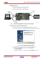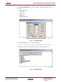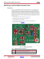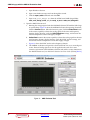
1
Artix-7 FPGA
AC701 Evaluation Kit
(Vivado Design Suite
2013.3)
Getting Started Guide
UG967 (v4.0.1) March 05, 2014
0402936-03
Notice of Disclaimer
The information disclosed to you hereunder (the “Materials”) is provided solely for the selection and use of Xilinx products. To the maximum
extent permitted by applicable law: (1) Materials are made available "AS IS" and with all faults, Xilinx hereby DISCLAIMS ALL
WARRANTIES AND CONDITIONS, EXPRESS, IMPLIED, OR STATUTORY, INCLUDING BUT NOT LIMITED TO WARRANTIES OF
MERCHANTABILITY, NON-INFRINGEMENT, OR FITNESS FOR ANY PARTICULAR PURPOSE; and (2) Xilinx shall not be liable (whether
in contract or tort, including negligence, or under any other theory of liability) for any loss or damage of any kind or nature related to, arising
under, or in connection with, the Materials (including your use of the Materials), including for any direct, indirect, special, incidental, or
consequential loss or damage (including loss of data, profits, goodwill, or any type of loss or damage suffered as a result of any action
brought by a third party) even if such damage or loss was reasonably foreseeable or Xilinx had been advised of the possibility of the same.
Xilinx assumes no obligation to correct any errors contained in the Materials or to notify you of updates to the Materials or to product
specifications. You may not reproduce, modify, distribute, or publicly display the Materials without prior written consent. Certain products are
subject to the terms and conditions of the Limited Warranties which can be viewed at http://www.xilinx.com/warranty.htm; IP cores may be
subject to warranty and support terms contained in a license issued to you by Xilinx. Xilinx products are not designed or intended to be
fail-safe or for use in any application requiring fail-safe performance; you assume sole risk and liability for use of Xilinx products in Critical
Applications: http://www.xilinx.com/warranty.htm#critapps.
Automotive Applications Disclaimer
XILINX PRODUCTS ARE NOT DESIGNED OR INTENDED TO BE FAIL-SAFE, OR FOR USE IN ANY APPLICATION REQUIRING
FAIL-SAFE PERFORMANCE, SUCH AS APPLICATIONS RELATED TO: (I) THE DEPLOYMENT OF AIRBAGS, (II) CONTROL OF A
VEHICLE, UNLESS THERE IS A FAIL-SAFE OR REDUNDANCY FEATURE (WHICH DOES NOT INCLUDE USE OF SOFTWARE IN THE
XILINX DEVICE TO IMPLEMENT THE REDUNDANCY) AND A WARNING SIGNAL UPON FAILURE TO THE OPERATOR, OR (III) USES
THAT COULD LEAD TO DEATH OR PERSONAL INJURY. CUSTOMER ASSUMES THE SOLE RISK AND LIABILITY OF ANY USE OF
XILINX PRODUCTS IN SUCH APPLICATIONS.
Fedora Information
Xilinx obtained the Fedora Linux software from Fedora (http://fedoraproject.org/), and you may too. Xilinx made no changes to the software
obtained from Fedora. If you desire to use Fedora Linux software in your product, Xilinx encourages you to obtain Fedora Linux software
directly from Fedora (http://fedoraproject.org/), even though we are providing to you a copy of the corresponding source code as provided
to us by Fedora. Portions of the Fedora software may be covered by the GNU General Public license as well as many other applicable open
source licenses. Please review the source code in detail for further information. To the maximum extent permitted by applicable law and if
not prohibited by any such third-party licenses, (1) XILINX DISCLAIMS ANY AND ALL EXPRESS OR IMPLIED WARRANTIES,
INCLUDING, BUT NOT LIMITED TO, THE IMPLIED WARRANTIES OF MERCHANTABILITY AND FITNESS FOR A PARTICULAR
PURPOSE; AND (2) IN NO EVENT SHALL XILINX BE LIABLE FOR ANY DIRECT, INDIRECT, INCIDENTAL, SPECIAL, EXEMPLARY, OR
CONSEQUENTIAL DAMAGES (INCLUDING, BUT NOT LIMITED TO, PROCUREMENT OF SUBSTITUTE GOODS OR SERVICES; LOSS
OF USE,DATA, OR PROFITS; OR BUSINESS INTERRUPTION) HOWEVER CAUSED AND ON ANY THEORY OF LIABILITY, WHETHER
IN CONTRACT, STRICT LIABILITY, OR TORT (INCLUDING NEGLIGENCE OR OTHERWISE) ARISING IN ANY WAY OUT OF THE USE
OF THIS SOFTWARE, EVEN IF ADVISED OF THE POSSIBILITY OF SUCH DAMAGE.
Fedora software and technical information is subject to the U.S. Export Administration Regulations and other U.S. and foreign law, and may
not be exported or re-exported to certain countries (currently Cuba, Iran, Iraq, North Korea, Sudan, and Syria) or to persons or entities
prohibited from receiving U.S. exports (including those (a) on the Bureau of Industry and Security Denied Parties List or Entity List, (b) on
the Office of Foreign Assets Control list of Specially Designated Nationals and Blocked Persons, and (c) involved with missile technology or
nuclear, chemical or biological weapons). You may not download Fedora software or technical information if you are located in one of these
countries, or otherwise affected by these restrictions. You may not provide Fedora software or technical information to individuals or entities
located in one of these countries or otherwise affected by these restrictions. You are also responsible for compliance with foreign law
requirements applicable to the import and use of Fedora software and technical information.
© Copyright 2013–2014 Xilinx, Inc. Xilinx, the Xilinx logo, Artix, ISE, Kintex, Spartan, Virtex, Vivado, Zynq, and other designated brands
included herein are trademarks of Xilinx in the United States and other countries. PCI, PCI Express, PCIe, and PCI-X are trademarks of
PCI-SIG. All other trademarks are the property of their respective owners.
AC701 Getting Started Guide
www.xilinx.com
UG967 (v4.0.1) March 05, 2014
Revision History
The following table shows the revision history for this document.
Date
Version
01/10/2013
1.0
Initial Xilinx release.
04/17/2013
2.0
Updated for Vivado® Design Suite 2013.1. Updated Introduction, Basic Hardware
Bring-up with Built-In Self-Test, AMS Bring-up with the AMS101 Evaluation Card, and
Advanced Bring-up with Base Targeted Reference Design sections. Updated Figure 2.
07/10/2013
3.0
Updated for Vivado® Design Suite 2013.2.
11/19/2013
4.0
Updated version references for Vivado Design Suite from 2013.2 to 2013.3. Corrected the
LED Status descriptions on page 24. Changed Note to Caution and strengthened the
description in the power connection note on page 24. Revised all links and references in
Appendix A, Additional Resources and revised links to web pages and documents
throughout document to conform to latest style convention. Updated Figure 21, page 28
and Figure 22, page 28.
03/05/2014
4.0.1
UG967 (v4.0.1) March 05, 2014
Revision
Tech pubs update. Technical content not affected.
www.xilinx.com
AC701 Getting Started Guide
AC701 Getting Started Guide
www.xilinx.com
UG967 (v4.0.1) March 05, 2014
Table of Contents
Revision History . . . . . . . . . . . . . . . . . . . . . . . . . . . . . . . . . . . . . . . . . . . . . . . . . . . . . . . . . . . . . 3
Getting Started with the Artix-7 FPGA AC701 Evaluation Kit
Introduction . . . . . . . . . . . . . . . . . . . . . . . . . . . . . . . . . . . . . . . . . . . . . . . . . . . . . . . . . . . . . . . . . 7
Basic Hardware Bring-up with Built-In Self-Test . . . . . . . . . . . . . . . . . . . . . . . . . . . . . 8
AMS Bring-up with the AMS101 Evaluation Card . . . . . . . . . . . . . . . . . . . . . . . . . . . 14
Advanced Bring-up with Base Targeted Reference Design . . . . . . . . . . . . . . . . . . . 19
Appendix A: Additional Resources
Xilinx Resources . . . . . . . . . . . . . . . . . . . . . . . . . . . . . . . . . . . . . . . . . . . . . . . . . . . . . . . . . . . .
Solution Centers . . . . . . . . . . . . . . . . . . . . . . . . . . . . . . . . . . . . . . . . . . . . . . . . . . . . . . . . . . . .
References . . . . . . . . . . . . . . . . . . . . . . . . . . . . . . . . . . . . . . . . . . . . . . . . . . . . . . . . . . . . . . . . . .
Additional References. . . . . . . . . . . . . . . . . . . . . . . . . . . . . . . . . . . . . . . . . . . . . . . . . . . . . . .
35
35
35
36
Appendix B: Warranty
AC701 Getting Started Guide
UG967 (v4.0.1) March 05, 2014
www.xilinx.com
Send Feedback
5
6
Send Feedback
www.xilinx.com
AC701 Getting Started Guide
UG967 (v4.0.1) March 05, 2014
Getting Started with the Artix-7 FPGA
AC701 Evaluation Kit
Introduction
The Artix®-7 FPGA AC701 Evaluation Kit (Figure 1) provides a comprehensive,
high-performance development and demonstration platform based on the XC7A200T
FPGA for high-bandwidth and high-performance applications in multiple market
segments. The built-in self-test (BIST), the AMS 101 evaluation card usage, and the
Artix-7 FPGA Base Targeted Reference Design (TRD) are featured in this getting started
guide.
X-Ref Target - Figure 1
UG967_01_111412
Figure 1:
AC701 Getting Started Guide
UG967 (v4.0.1) March 05, 2014
AC701 Evaluation Kit
www.xilinx.com
Send Feedback
7
Basic Hardware Bring-up with Built-In Self-Test
This Getting Started Guide is divided into two sections:
•
Basic Hardware Bring-up: Enables hands-on operation of all the features in the BIST
as well as evaluation of Analog Mixed Signal (AMS) using the AMS101 evaluation
card.
•
Advanced Bring-up: Enables hands-on operation with the base TRD, which features
PCIe®, DDR3 memory, AXI stream interconnect, and AXI virtual FIFO controller IP
cores—all supported through a custom evaluation graphical user interface (GUI).
AC701 Evaluation Kit Contents
•
AC701 evaluation board featuring the XC7A200T FPGA
•
Targeted reference design featuring DDR3, PCIe, and DMA
•
Including a full license for the Northwest Logic DMA
•
AMS101 evaluation board
•
Full seat Vivado® Design Suite: Design Edition
•
•
Node-locked, device-locked to the Artix-7 XC7A200T FPGA
Additional downloadable content, including:
•
Reference designs, design examples, and demos
•
Board design files
•
Documentation
-
Hardware User Guide
-
Getting Started Guide
-
Reference Design User Guide
•
12V AC-adapter power supply
•
Cables
•
RJ45 Ethernet cable
•
HDMI cable
•
Type-A to micro-B USB cable used for JTAG programming
•
Type-A to mini-B USB cable used for UART communication with board
•
Software and reference designs, demos, and documents to quickly get started
•
The AC701 BIST Design Files (RDF0220) are available from the AC701 Evaluation Kit
Documentation webpage.
All user guides, board files, tutorials, example designs, and targeted reference designs are
available from the AC701 Evaluation Kit Documentation webpage.
The tutorials and reference designs are useful for exploring the capabilities of the AC701
board and the Artix-7 FPGA. For additional information, see the Artix-7 Family FPGAs
Product Table.
Basic Hardware Bring-up with Built-In Self-Test
Introduction
The BIST reference design tests many of the features of the Artix-7 FPGA AC701
Evaluation Kit and can be programmed into the FPGA via the JTAG interface.
8
Send Feedback
www.xilinx.com
AC701 Getting Started Guide
UG967 (v4.0.1) March 05, 2014
Basic Hardware Bring-up with Built-In Self-Test
Figure 2 and Table 1 provide an overview of the board features utilized by the BIST and the
AMS101 evaluation card.
X-Ref Target - Figure 2
4
8
9
11
10
12
1
16
2
5
13
3
6
14
7
15
UG967_02_040913
Figure 2:
Table 1:
AC701 Board Features
Callout
AC701 Getting Started Guide
UG967 (v4.0.1) March 05, 2014
AC701 Board Detail
Component Description
1
SW1 Configuration Mode DIP Switch
2
Digilent JTAG connector
3
RJ45 Ethernet connector
4
XADC header
5
DDR3 external memory
6
LCD display
7
Rotary switch (under LCD)
8
Status LEDs and user LEDs
9
CPU reset button
10
Prog button
11
Power slide switch
12
12V power connector
13
User DIP switch
14
Contrast wheel
15
User push buttons
16
USB-UART connector
www.xilinx.com
Send Feedback
9
Basic Hardware Bring-up with Built-In Self-Test
For a description of all features on the AC701 Board, see AC701 Evaluation Board for the
Artix-7 FPGA User Guide (UG952) [Ref 1].
Test Setup Requirements
Note: This example design uses a Windows 7 PC flow and TeraTerm Pro.
The prerequisites for testing the design in hardware are:
•
AC701 evaluation board with XC7A200T FPGA
•
Type-A to mini-B USB cable (for UART)
•
Type-A to micro-B USB cable (for JTAG)
•
AC Power Adapter (12 VDC)
•
TeraTerm Pro or other terminal program
•
USB-UART drivers from Silicon Labs
•
Vivado Design Suite installed on host PC
Hardware Test Board Setup
This section details the hardware setup and use of the terminal program for running the
BIST application. It details step-by-step instructions for board bring-up. For more
information on installing the tools and drivers, see the Boards and Kits Install Guide.
AC701 Evaluation Board Setup
1.
Set DIP switch SW1 as shown in Figure 3 (ON, OFF, ON = 101).
X-Ref Target - Figure 3
M2 M1 M0
1
2
ON Position = 1
3
SW1
OFF Position = 0
UG967_03_102813
Figure 3:
10
Send Feedback
SW1 Switch Settings for JTAG Programming Mode
www.xilinx.com
AC701 Getting Started Guide
UG967 (v4.0.1) March 05, 2014
Basic Hardware Bring-up with Built-In Self-Test
Hardware Bring-up
1.
Place the AC701 board power switch SW12 to OFF.
2.
Connect the AC701 board as shown in Figure 4.
3.
Place the AC701 board power switch SW12 to ON.
X-Ref Target - Figure 4
Board Power
Switch SW12
USB Cable
Standard-A Plug
to Mini-B Plug
To J17
(UART)
Host
Computer
To J18
Power Supply
100 VAC–240 VAC Input
12 VDC 5.0A Output
To JTAG
USB Cable
Standard-A Plug
to Micro-B Plug
Figure 4:
UG967_04_102813
AC701 Board with UART and 12V Adapter Cables Attached
Install the Silicon Labs UART Device Driver.
1.
Run the downloaded executable UART-USB driver file, listed in Test Setup
Requirements (see Figure 5). This enables UART-USB communications with a host PC.
X-Ref Target - Figure 5
UG967_05_111412
Figure 5:
2.
UART Cable Driver Installation Dialog
Set the USB-UART connection to a known PORT in the Device Manager:
a.
Right-click the Computer desktop icon and select Properties.
b.
Click Device Manager.
c.
Right-click the Cypress device in the list, and select Properties (see Figure 6).
AC701 Getting Started Guide
UG967 (v4.0.1) March 05, 2014
www.xilinx.com
Send Feedback
11
Basic Hardware Bring-up with Built-In Self-Test
X-Ref Target - Figure 6
UG967_06_111412
Figure 6:
Selecting the Cypress Driver in the Device Manager
d. Click the Port Settings tab, then click the Advanced… button.
e.
Select an open COM port between COM1 and COM4 (see Figure 7).
Note: Steps and diagrams refer to a Windows host PC.
X-Ref Target - Figure 7
UG967_07_111412
Figure 7:
Setting the Port for the Cypress Driver
Run the BIST Application
12
1.
Download the AC701 BIST Design Files (RDF0220) from the AC701 Evaluation Kit
Documentation webpage under the Example Designs section.
2.
Unzip the design files to the C:\ directory.
3.
Start the installed terminal program.
Send Feedback
www.xilinx.com
AC701 Getting Started Guide
UG967 (v4.0.1) March 05, 2014
Basic Hardware Bring-up with Built-In Self-Test
4.
Select Setup > Serial Port… and ensure that the settings match those shown in
Figure 8:
•
Baud rate: 9600
•
Data: 8 bit
•
Parity: none
•
Stop: 1 bit
•
Flow control: none
X-Ref Target - Figure 8
UG967_08_111412
Figure 8:
5.
Serial Port Setup
In Vivado Design Suite, open a Tcl shell and type:
source C:/ac701_bist/ready_for_download/bist_download.tcl
6.
Select the desired tests to run and observe the test results (see Figure 9).
X-Ref Target - Figure 9
UG967_09_111412
Figure 9:
AC701 Getting Started Guide
UG967 (v4.0.1) March 05, 2014
www.xilinx.com
BIST Main Menu
Send Feedback
13
AMS Bring-up with the AMS101 Evaluation Card
AMS Bring-up with the AMS101 Evaluation Card
Introduction
The Artix-7 XC7A200T FPGA features two 1 Mega-samples per second (MSPS), 12-bit,
Analog-to-Digital Converters (ADCs) built into the device for a range of applications
including simple analog monitoring to more signal processing-intensive tasks such as
linearization, calibration, oversampling, and filtering. The AC701 Evaluation Kit includes
the hardware and software to evaluate the ADC feature. The AC701 Evaluation Kit also
includes voltage, current and power monitoring for nine of the analog power supplies on
the board. For evaluation of Xilinx Analog Mixed Signal (AMS) capability, these items in
the kit are needed:
•
Access to the AC701 board XADC header (see Figure 2)
•
AMS101 evaluation card (see Figure 10 and Table 1)
•
FPGA design files and software files
•
7 Series FPGA AMS Targeted Reference Design User Guide (UG960) [Ref 1]
•
USB-UART drivers from Silicon Labs
X-Ref Target - Figure 10
1
2
6
5
3
4
UG967_10_112712
Figure 10:
Table 2:
Callout
14
AMS101 Evaluation Card
AMS101 Evaluation Card Features
Component Description
1
Jumpers to select DAC or external signal source.
2
20-pin connector to the XADC header on the AC701 board.
Send Feedback
www.xilinx.com
AC701 Getting Started Guide
UG967 (v4.0.1) March 05, 2014
AMS Bring-up with the AMS101 Evaluation Card
Table 2:
AMS101 Evaluation Card Features (Cont’d)
Callout
Component Description
3
Pins for external analog input signals.
4
Digital I/O level translators.
5
16-bit DAC to set analog test voltage.
6
Reference buffer for DAC.
Getting Started
1.
Verify the USB-UART Silicon Labs drivers are installed as described in Install the
Silicon Labs UART Device Driver., page 11.
2.
Install the National Instruments LabVIEW run-time engine on the host PC:
a.
Go to the AC701 Evaluation Kit Documentation webpage.
b.
Under the Documentation heading, click on the appropriate Vivado software
version. This will expand a list of available document types.
c.
Click on Targeted Reference Designs. This will open a list of files and
documents.
d. Click on 7 Series FPGA and Zynq-7000 AP SoC AMS Evaluator Installer for
AMS Targeted Reference Design to download ams101_gui_installer.zip.
3.
e.
Unzip the files to a temporary directory and double-click setup.exe to install the
LabVIEW run-time engine and AMS Evaluator software.
f.
After installation is complete, restart the host PC.
Extract the AMS design files before Evaluating AMS:
a.
Go to the AC701 Evaluation Kit Documentation webpage.
b.
Under the Documentation heading, click on the appropriate Vivado software
version. This will expand a list of available document types.
c.
Click on Targeted Reference Designs. This will open a list of files and
documents.
d. Click on AMS Targeted Reference Design for Artix-7 FPGA AC701 Evaluation
Kit (RDF0278) to download rdf0278-ams101-ac701-trd.zip.
e.
Unzip the files to a working directory on the host computer.
Evaluating AMS
1.
Power off the AC701 board, connect the AMS101 card, and re-apply power to the
hardware.
a.
2.
Connect the AMS101 evaluation card to the AC701 board, making sure the notch
on the XADC header lines up correctly with the connector on the AMS101
evaluation card.
Implement the design to the Artix-7 XC7A200T-2 FB676 FPGA from the AC701 AMS
design file xadc_eval_design_ac701_v1_0 previously downloaded.
a.
Open Vivado Design Suite. Here is one example path:
Start menu/Xilinx Design Tools/Vivado 2013.3
b.
AC701 Getting Started Guide
UG967 (v4.0.1) March 05, 2014
Create a Vivado Project.
www.xilinx.com
Send Feedback
15
AMS Bring-up with the AMS101 Evaluation Card
c.
Open Hardware Session.
d. Open a new hardware target and run through the wizard.
e.
Click the open_cable command and select OK.
f.
Open xadc_eval_design.bit from the AC701 board AMS design folder:
xadc_eval_design_ac701_v1_0 > ready_to_test > xadc_eval_design.bit
3.
Open the AMS Evaluator tool.
a.
Running the setup program loads the AMS101 Evaluator GUI with the Xilinx logo
on your desktop. Figure 11 shows the AMS101 Evaluator after opening. From here,
click the Connect button. When the button is green, click the Collect Data button
in the center to quickly evaluate the analog signals in the time and frequency
domain, display linearity, verify the XADC Registers settings, and measure the
internal temperature sensor and supply voltages.
b.
Collect Data button in the center to quickly evaluate the analog signals in the time
and frequency domain, display linearity, verify the XADC register settings, and
measure the internal temperature sensor and supply voltages.
c.
Figure 12 shows the XADC results in the frequency domain.
d. The AMS101 evaluation card provides a dual 16-bit DAC for use as an analog test
source. External analog signals can also be applied to the card. For a more
extensive explanation of the AMS101 evaluation card and the various functions in
the AMS Evaluator tool, see AMS101 Evaluation Card User Guide (UG886) [Ref 16].
X-Ref Target - Figure 11
UG967_11_112712
Figure 11:
16
Send Feedback
AMS Evaluator Tool
www.xilinx.com
AC701 Getting Started Guide
UG967 (v4.0.1) March 05, 2014
AMS Bring-up with the AMS101 Evaluation Card
X-Ref Target - Figure 12
UG967_12_112712
Figure 12:
XADC Fast Fourier Transform Result
Power Monitoring
In addition to measuring the analog signals from the AMS101 evaluation card, the AC701
also uses the XADC as a system monitoring solution for measuring the voltage, load
current and calculated power for nine of the AC701 board analog power supplies. By
offering 12-bits, 1 MSPS and up to 17 externally multiplexed inputs, the XADC is a good
solution for monitoring voltage and current on all Artix-7 FPGA applications. Figure 13
shows an example of the AC701 monitoring VCCINT, VCCAUX, VCCBRAM and the 1.5V
supply.
In conjunction with the AMS Evaluator, the AC701 AMS reference design also measures
the voltages, current and power for VCCO_ADJ, the 1.8V supply, the 3.3V supply,
MGTAVCC and MGTAVTT.
AC701 Getting Started Guide
UG967 (v4.0.1) March 05, 2014
www.xilinx.com
Send Feedback
17
AMS Bring-up with the AMS101 Evaluation Card
X-Ref Target - Figure 13
UG967_13_112712
Figure 13:
18
Voltage, Current and Power Monitoring on AC701 Board Supplies
Send Feedback
www.xilinx.com
AC701 Getting Started Guide
UG967 (v4.0.1) March 05, 2014
Advanced Bring-up with Base Targeted Reference Design
Advanced Bring-up with Base Targeted Reference Design
Introduction
Figure 14 depicts the block-level overview of the Artix-7 FPGA base Targeted Reference
Design (TRD) which delivers up to 10 Gb/s of performance per direction.
X-Ref Target - Figure 14
64 bits at
800 Mb/s
XADC
DDR3 IO
UCD90120A
Power and
Temperature
Monitor
PCIe
Monitor
User Space
Registers
AXI MIG
512 bits at
100 MHz
AXI VFIFO
WR
RD
512 bits at
100 MHz
512 bits at
100 MHz
64 x 250 MHz
AXIS IC
AXI Target
Master
PCIe IP
GUI
GTP
Transceiver
S0
DDR3
S1
S2
S3
64 x 250 MHz
AXIS IC
M3
M2
M1
M0
S2C0
XRaw Driver
AXI Stream Generator
and Checker
128 bits at
125 MHz
C2S0
XDMA
Driver
PCIe x4
Gen2 Link
Checker
PCIe
Integrated
Endpoint
Block x4 Gen2
128 bits at
125 MHz
Packet
DMA
Generator
Loopback
S2C1
AXI Stream Generator
and Checker
128 bits at
125 MHz
C2S1
Checker
128 bits at
125 MHz
Generator
Loopback
Integrated Blocks
in FPGA
Xilinx IP
Third Party IP
AXI ST (128 bits at 125 MHz)
Control Path
Software Driver
Custom RTL
On Board
AXI MM (512 bits at 100 MHz)
50 MHz Domain
Figure 14:
UG967_14_121912
Artix-7 FPGA Base TRD Block Diagram
The intent of this design is to demonstrate a high performance data transfer system using
the PCI Express® x4 GEN2 endpoint with a high performance scatter-gather packet DMA
controller from NorthWest Logic and DDR3 64-bit SODIMM memory operating at
800 Mb/s.
The PCIe® endpoint and DMA controller together are responsible for the movement of
data between a PC and an FPGA. S2C implies data movement from a PC to an FPGA and
C2S implies data movement from an FPGA to a PC. A DDR3 SDRAM (64-bit, 800 Mb/s or
400 MHz) is used for packet buffering — a virtual FIFO layer facilitates the use of DDR3
AC701 Getting Started Guide
UG967 (v4.0.1) March 05, 2014
www.xilinx.com
Send Feedback
19
Advanced Bring-up with Base Targeted Reference Design
memory as multiple FIFOs. Additionally, the design provides power monitoring capability
based on a PicoBlaze™ embedded processor.
For software, the design provides 32-bit Linux drivers targeting the Fedora 16 platform
and a graphical user interface (GUI) which controls the tests and monitors the status.
Features
Base Features
This section lists the features of the Targeted Reference Design.
•
•
PCI Express v2.1 compliant x4 endpoint operating at 5Gb/s/lane/direction
•
PCIe transaction interface utilization monitor
•
MSI & Legacy interrupt support
Bus Mastering Scatter-gather DMA
•
Multichannel DMA
•
AXI4-Stream interface for data
•
AXI4 interface for register space access
•
DMA performance monitor
•
Full duplex operation
-
•
Independent transmit and receive channels
Virtual FIFO layer over DDR3 memory
•
Provides 4 channel design (4 FIFOs in DDR3 SODIMM)
Application Features
•
PicoBlaze processor-based PVT Monitoring
•
Built-in hardware to monitor power by reading the TI UCD90120A power
controller chip included on the AC701 evaluation board
•
Built-in hardware to monitor die temperature by way of a Xilinx
Analog-to-Digital Converter
Test Setup Requirements
The prerequisites for testing the design in hardware are
20
•
AC701 evaluation board with XC7A200T FPGA
•
Design consisting of:
•
Design source files
•
Device driver files
•
FPGA programming files
•
Documentation
•
Vivado Design Edition
•
Type-A to micro-B USB cable
•
Fedora 16 LiveDVD
Send Feedback
www.xilinx.com
AC701 Getting Started Guide
UG967 (v4.0.1) March 05, 2014
Advanced Bring-up with Base Targeted Reference Design
•
A PC with PCIe v2.1 compliant slot. For a complete list of recommended machines,
and all known issues, see Artix-7 FPGA Base Targeted Reference Design Master
Answer Record (AR 53372).
Note: The PC could also have Fedora 16 Linux OS installed.
Hardware Demonstration Setup
This section details the hardware setup and use of the provided control and monitoring
application and GUI to assist in getting started quickly with the hardware. Step-by-step
explanations are provided on hardware bring-up, software bring-up, and the use of the
application GUI.
Board Setup
This section details how to set up the AC701 evaluation board as required for
demonstrating the TRD.
Setting the AC701 Jumpers And Switches
1.
Turn off the power to the AC701 board and verify the switch and jumper settings are as
shown in Table 3, Table 4, and Figure 15.
Table 3:
AC701 Board Required Jumper Settings
Jumper
J12
Table 4:
Function
PCIe endpoint configuration width; 4-lane design
3-4
AC701 Board Required Switch Settings
Switch
Function/Type
SW15
Board power slide-switch
SW2
User GPIO DIP switch
SW1
Setting
Setting
off
4
off
3
off
2
off
1
off
Positions 1, 2, and 3 set configuration mode
3
001 – Master SPI
on
2
101 – JTAG
off
1
AC701 Getting Started Guide
UG967 (v4.0.1) March 05, 2014
off
www.xilinx.com
Send Feedback
21
Advanced Bring-up with Base Targeted Reference Design
X-Ref Target - Figure 15
SW15
J49
SW1
SW2
SW1
1 2 3 4
Pin 1
On
On
1 2 3
J12
Pin 1
SW2
UG967_15_040513
Figure 15:
22
Send Feedback
AC701 Board Switch and Jumper Locations
www.xilinx.com
AC701 Getting Started Guide
UG967 (v4.0.1) March 05, 2014
Advanced Bring-up with Base Targeted Reference Design
Hardware Bring Up
All procedures listed in the subsequent sections require super-user access on a Linux PC.
When using the Fedora 16 LiveDVD provided with the kit, super-user access is granted by
default due to the manner in which the kernel image is built. If not using the LiveDVD, it
is important to ensure that super-user access is granted.
1.
With the host PC powered off, insert the AC701 board into the selected PCIe x4 (or
wider) edge connector (see Figure 16). The PCI Express specification allows for a
smaller lane width endpoint to be installed into a larger lane width PCIe connector.
X-Ref Target - Figure 16
8*BB
Figure 16:
AC701 Getting Started Guide
UG967 (v4.0.1) March 05, 2014
AC701 Board Installed in a PCIe x16 Connector
www.xilinx.com
Send Feedback
23
Advanced Bring-up with Base Targeted Reference Design
2.
Connect the 12V ATX power supply 4-pin connector to the board as shown in
Figure 17.
X-Ref Target - Figure 17
UG967_17_121412
Figure 17:
Power Supply Connection
Caution! Do NOT plug a PC ATX power supply 6-pin connector into J49 on the AC701 board
The ATX 6-pin connector has a different pinout than J49. Connecting an ATX 6-pin connector into
J49 will damage the AC701 board and void the board warranty.
24
3.
To avoid loose contact issues, make sure the connections are secure. Turn ON the SW15
switch, apply power to the system, insert the Fedora LiveDVD, and change the boot
order to boot from the DVD.
4.
Check the status of the design using the AC701 board LEDs. The design provides
status with the GPIO LEDs located on the upper right portion of the AC701 board.
When the PC is powered on and the TRD has successfully configured, the LED status
from left to right indicates:
•
LED position 1: ON if DDR3 is calibrated
•
LED position 2: ON if the lane width is x4, else flashing
•
LED position 3: Heart beat LED, flashes if PCIe user clock is present
•
LED position 4: ON if the PCIe link is up
Send Feedback
www.xilinx.com
AC701 Getting Started Guide
UG967 (v4.0.1) March 05, 2014
Advanced Bring-up with Base Targeted Reference Design
Figure 18 shows the location of the status LEDs.
X-Ref Target - Figure 18
LED Position 1 2 3 4
UG967_18_121812
Figure 18:
GPIO LEDs Indicating TRD Status
Linux Driver Installation
The following sections describe installing the device drivers for the Artix-7 FPGA base
TRD after completion of the prior steps.
1.
If the Fedora 16 Linux OS is currently installed on the PC, boot as a root-privileged
user and skip to step 4.
2.
To boot from the Fedora 16 LiveDVD provided in the kit, place the DVD in the PC
DVD-ROM drive. The Fedora 16 Live Media is for Intel-compatible PCs. The DVD
contains a complete, bootable 32-bit Fedora 16 environment with the proper packages
installed for the TRD demonstration environment. The PC boots from the DVD-ROM
drive and logs into a liveuser account. This account has kernel development root
privileges required to install and remove device driver modules.
Note: It might be necessary to adjust the PC BIOS boot order settings to ensure that the
DVD-ROM drive is the first drive in the boot order. Refer to the PC user manual for the proper
procedure to set the BIOS boot order.
AC701 Getting Started Guide
UG967 (v4.0.1) March 05, 2014
www.xilinx.com
Send Feedback
25
Advanced Bring-up with Base Targeted Reference Design
The PC should boot from the DVD-ROM drive. The images in Figure 19 are seen on the
monitor during startup.
X-Ref Target - Figure 19
First Screen
Last Boot Screen
Boot Complete
UG967_19_111212
Figure 19:
3.
Fedora 16 LiveDVD Boot Sequence
After Fedora boots, open a terminal window (click Activities > Application, scroll
down, and click the Terminal icon).
To determine if the PCIe integrated block is detected, at the terminal command
prompt, type:
$ lspci
The lspci command displays the PCI and PCI Express buses of the PC. On the bus
corresponding to the PCIe connector holding the AC701 board, look for the message:
Memory controller: Xilinx Corporation Device 7042
This message confirms that the design programmed into the AC701 board is detected
by the BIOS and the Fedora 16 OS. The bus number varies depending on the PC
motherboard and slot used.
26
Send Feedback
www.xilinx.com
AC701 Getting Started Guide
UG967 (v4.0.1) March 05, 2014
Advanced Bring-up with Base Targeted Reference Design
Figure 20 shows an example of the output from the lspci command. The highlighted
region shows that Xilinx device 7042 has been located by the BIOS on bus number 3
(03:00.0 = bus:dev.function).
X-Ref Target - Figure 20
UG967_20_121812
Figure 20:
4.
PCI and PCI Express Bus Devices
Go to the AC701 Evaluation Kit Documentation webpage.
a.
Under Documentation, click 2013.3 to expand the list of 2013.3 documentation.
b.
Under By Document Type, click Targeted Reference Designs to open a window
listing design files and documents.
c.
Click on the RDF0278 link and save the file a7_base_trd folder to the desktop
(or a folder of choice).
Note: This operation requires root privileges.
Double-click the copied a7_base_trd folder.
AC701 Getting Started Guide
UG967 (v4.0.1) March 05, 2014
www.xilinx.com
Send Feedback
27
Advanced Bring-up with Base Targeted Reference Design
The screen capture in Figure 21 shows the content of the a7_base_trd folder.
X-Ref Target - Figure 21
UG967_21_110513
Figure 21:
5.
Structure of a7_base_trd Directory
Right-click on the script (quickstart.sh), select Properties. In the Permission tab,
check the Allow executing file as program box. The script is now executable. To run
the script, double-click quickstart.sh and select Run in Terminal.
X-Ref Target - Figure 22
UG967_22_110513
Figure 22:
6.
28
Running the quickstart.sh Script
The GUI showing driver installation options appears as shown in Figure 23.
Subsequent steps demonstrate the GUI operation by installing and removing drivers.
Click Install.
Send Feedback
www.xilinx.com
AC701 Getting Started Guide
UG967 (v4.0.1) March 05, 2014
Advanced Bring-up with Base Targeted Reference Design
X-Ref Target - Figure 23
UG967_23_121812
Figure 23:
AC701 Getting Started Guide
UG967 (v4.0.1) March 05, 2014
Artix-7 FPGA Base TRD Driver Installation GUI
www.xilinx.com
Send Feedback
29
Advanced Bring-up with Base Targeted Reference Design
After installing the driver, the control and monitoring user interface appears as shown in
Figure 24. The control view shows control parameters such as test mode (loopback,
generator, or checker) and packet length. The system monitor tab shows system power and
temperature. The GUI also provides an LED indicator for DDR3 memory calibration.
X-Ref Target - Figure 24
UG967_24_111312
Figure 24:
Artix-7 FPGA Base TRD Control and Monitoring Interface
Using the Application GUI
The transmission and reception of data is configured through the application GUI. The
GUI displays collected statistics and other status information.
At startup, the GUI displays a launching page that detects the PCIe device for this design
(Vendor ID = 0x10EE and Device ID = 0x7042). When the appropriate device is detected,
driver installation is allowed to proceed. An additional option is available which allows
the enabling of a data integrity check. Upon successful installation of the drivers, the
control and monitoring interface appears.
GUI Control Function
These parameters are controlled with the GUI:
•
30
Packet size for traffic generation.
Send Feedback
www.xilinx.com
AC701 Getting Started Guide
UG967 (v4.0.1) March 05, 2014
Advanced Bring-up with Base Targeted Reference Design
•
Test selection:
•
Loopback
•
HW checker
•
HW Generator
GUI Monitor Function
The driver always maintains information about the hardware status. The GUI periodically
issues an I/O Control, ioctl(), to read the status information which is comprised of:
•
PCIe link and device status
•
DMA controller status
•
Power status
The driver maintains a set of circular arrays to hold second-by-second sampling points of
various statistics which are periodically collected by the performance monitor handler.
The various GUI indicators and controls are detailed in Figure 25 and Table 5.
X-Ref Target - Figure 25
9
1
10
2
3
4
11
12
5
13
6
7
15
2
3
4
14
5
8
UG967_25_111312
Figure 25:
AC701 Getting Started Guide
UG967 (v4.0.1) March 05, 2014
Control and Monitoring Interface
www.xilinx.com
Send Feedback
31
Advanced Bring-up with Base Targeted Reference Design
Table 5:
Callout
Control and Monitoring Interface Components
Component
Component Description
1
Led Indicator
Indicates DDR3 calibration information; Green on calibration, red
otherwise
2
Test Option
Options to select Loopback, HW Generator, or HW checker
3
Packet size
Packet size for the test run with allowed packet size shown as a tool tip
4
Test start/stop control
Button to control the start and end of the test
5
DMA statistics
• Throughput (Gb/s): DMA payload throughput in gigabits per
second for transmit and receive controllers
• DMA Active Time (ns): The time in nanoseconds that the DMA
controller has been active in the last second
• DMA Wait Time (ns): The time in nanosecond that the DMA
controller waited for the software to provide more descriptors
• BD Errors: Indicates a count of buffer descriptors (BD) that caused a
DMA error as indicated by the error status field in the descriptor
update
• BD Short Errors: Indicates a short error in the buffer descriptors in
the transmit direction when the entire buffer specified by length in
the descriptor could not be fetched (Not applicable to the receive
direction)
• SW BDs: Indicates the total count of buffer descriptors set up in the
descriptor ring
6
PCIe Transmit (writes in Gb/s)
Reports transmitted (endpoint card to host) throughput as obtained
from the PCIe endpoint hardware performance monitor
7
PCIe Receive (reads in Gb/s)
Reports received (host to endpoint card) throughput as obtained from
the PCIe endpoint hardware performance monitor
8
Message log
Text box showing informational messages, warnings, or errors
9
Performance plots
Click this tab to plot the PCIe transactions on the AXI4-Stream interface
and show the payload statistics graph based on the DMA controller
performance monitor
10
Close button
Click this button to close the GUI
11
PCIe Endpoint Status
Reports the contents of various PCIe endpoint configuration fields as
reported in the endpoint configuration space
12
Host System’s Initial Credits
Initial flow control credits advertised by the host system after link
training with the endpoint (A value of zero implies infinite flow control
credits)
13
Block diagram button
Click this button to show a case block diagram of each mode currently
running
14
Power statistics
Power in Watt plotted for the VCCINT, GTVCC, VCCAUX, and
VCCBRAM rails
15
Temperature
Monitors the current die temperature
Notes:
1. Items 2 through 5 are duplicated for each of the two datapaths.
32
Send Feedback
www.xilinx.com
AC701 Getting Started Guide
UG967 (v4.0.1) March 05, 2014
Advanced Bring-up with Base Targeted Reference Design
The GUI was developed using the JAVA environment. The Java Native Interface (JNI) was
used to build the bridge between the driver and the GUI. This code can also be used with
the Windows operating system with only minor changes.
Evaluating the TRD
1.
To start the data traffic on the two datapaths:
a.
Click Start on Datapath-0 as shown in Figure 26. This enables the driver to start
generating the data for Datapath-0.
b.
Click Start on Datapath-1 as shown in Figure 26. This enables the driver to start
generating the data for Datapath-1.
X-Ref Target - Figure 26
UG967_26_111312
Figure 26:
2.
Start Data Traffic from GUI
Verify TRD operations through the status information provided by the GUI as shown
in Figure 27:
a.
Verify PCIe endpoint throughput.
b.
Verify the DMA Channel throughput for Datapath-0.
c.
Verify the DMA Channel throughput for Datapath-1.
d. Verify that there are no buffer descriptor errors for error-free operation.
AC701 Getting Started Guide
UG967 (v4.0.1) March 05, 2014
www.xilinx.com
Send Feedback
33
Advanced Bring-up with Base Targeted Reference Design
X-Ref Target - Figure 27
UG967_27_121812
Figure 27:
Verifying Error-free Operation and Performance Plots
3.
Click the Performance Plots tab. The system-to-card and card-to-system performance
numbers for a specific packet size are shown. The packet size can be adjusted and the
resulting performance variation observed.
4.
Close the GUI. This uninstalls the driver and opens the driver installation options
screen of the Artix-7 FPGA base TRD. Driver un-installation requires the control and
monitoring GUI to first be closed.
This completes system performance evaluation of the Artix-7 FPGA base TRD using the
pre-built demonstration bit file. The reference design can now be modified. The Vivado
Design Suite must be installed before proceeding with custom modifications. The design
tools do not need to be installed on the same host PC in which the AC701 evaluation board
is installed.
34
Send Feedback
www.xilinx.com
AC701 Getting Started Guide
UG967 (v4.0.1) March 05, 2014
Appendix A
Additional Resources
Xilinx Resources
For support resources such as Answers, Documentation, Downloads, and Forums, see the
Xilinx Support website.
For continual updates, add the Answer Record to your myAlerts.
For definitions and terms, see the Xilinx Glossary.
Solution Centers
See the Xilinx Solution Centers for support on devices, software tools, and intellectual
property at all stages of the design cycle. Topics include design assistance, advisories, and
troubleshooting tips.
References
The most up to date information related to the AC701 Evaluation Kit and its
documentation is available on these websites:
AC701 Evaluation Kit
AC701 Evaluation Kit Documentation
AC701 Evaluation Kit Master Answer Record (AR 51900)
Artix-7 FPGA Base Targeted Reference Design Master Answer Record (AR 53372)
These Xilinx documents and sites provide supplemental material useful with this guide:
1.
AC701 Evaluation Board for the Artix-7 FPGA User Guide (UG952)
2.
7 Series FPGA AMS Targeted Reference Design User Guide (UG960)
3.
Vivado Design Suite User Guide Release Notes, Installation, and Licensing (UG973)
4.
7 Series FPGAs Integrated Block for PCI Express User Guide (PG054)
5.
Synthesis and Simulation Design Guide (UG626)
6.
Vivado Design Suite Logic Simulation User Guide (UG900)
7.
Understanding Performance of PCI Express Systems (WP350)
8.
LogiCORE IP Aurora 8B/10B v7.1 User Guide (UG766)
9.
LogiCORE IP Aurora 8B/10B v10.0 Product Guide for Vivado Design Suite (PG046)
10. LogiCORE IP AXI4-Stream Interconnect v1.1 Product Guide (PG035)
11. LogiCORE IP AXI Virtual FIFO Controller v1.1 Product Guide (PG038)
AC701 Getting Started Guide
UG967 (v4.0.1) March 05, 2014
www.xilinx.com
Send Feedback
35
Appendix A: Additional Resources
12. 7 Series FPGAs GTX/GTH Transceivers User Guide (UG476)
13. 7 Series FPGAs Memory Interface Solutions User Guide (UG586)
14. Artix-7 FPGA Integrated Block for PCI Express (UG477)
15. AC701 Evaluation Board for the Artix-7 FPGA User Guide (UG952)
16. AMS101 Evaluation Card User Guide (UG886)
Additional References
These external websites provide supplemental material useful with this guide:
17. Northwest Logic
(PCI Express® Solution, DMA Back End Core)
18. Fedora Project
(Fedora operating system information and downloads)
19. PicoBlaze 8-bit Microcontroller
(PicoBlaze™ 8-bit Microcontroller information and download)
20. Vivado Design Suite product page
(Vivado® Design Suite information and downloads)
21. Artix-7 FPGA Product Table
(List of Artix®-7 FPGAs)
22. Silicon Labs
Si570, Si5324C, CP2103GM, VCP Drivers
36
Send Feedback
www.xilinx.com
AC701 Getting Started Guide
UG967 (v4.0.1) March 05, 2014
Appendix B
Warranty
THIS LIMITED WARRANTY applies solely to standard hardware development boards
and standard hardware programming cables manufactured by or on behalf of Xilinx
(“Development Systems”). Subject to the limitations herein, Xilinx warrants that
Development Systems, when delivered by Xilinx or its authorized distributor, for ninety
(90) days following the delivery date, will be free from defects in material and
workmanship and will substantially conform to Xilinx publicly available specifications for
such products in effect at the time of delivery. This limited warranty excludes:
(i) engineering samples or beta versions of Development Systems (which are provided
“AS IS” without warranty); (ii) design defects or errors known as “errata”;
(iii) Development Systems procured through unauthorized third parties; and
(iv) Development Systems that have been subject to misuse, mishandling, accident,
alteration, neglect, unauthorized repair or installation. Furthermore, this limited warranty
shall not apply to the use of covered products in an application or environment that is not
within Xilinx specifications or in the event of any act, error, neglect or default of Customer.
For any breach by Xilinx of this limited warranty, the exclusive remedy of Customer and
the sole liability of Xilinx shall be, at the option of Xilinx, to replace or repair the affected
products, or to refund to Customer the price of the affected products. The availability of
replacement products is subject to product discontinuation policies at Xilinx. Customer
may not return product without first obtaining a customer return material authorization
(RMA) number from Xilinx.
THE WARRANTIES SET FORTH HEREIN ARE EXCLUSIVE. XILINX DISCLAIMS ALL
OTHER WARRANTIES, WHETHER EXPRESS, IMPLIED OR STATUTORY, INCLUDING,
WITHOUT LIMITATION, ANY WARRANTY OF MERCHANTABILITY, FITNESS FOR A
PARTICULAR PURPOSE, OR NON-INFRINGEMENT, AND ANY WARRANTY THAT
MAY ARISE FROM COURSE OF DEALING, COURSE OF PERFORMANCE, OR USAGE
OF TRADE. (2008.10)
X-Ref Target - Figure B-1
Do not throw Xilinx products marked with the “crossed out wheeled bin” in the trash.
Directive 2002/96/EC on waste electrical and electronic equipment (WEEE) requires the
separate collection of WEEE. Your cooperation is essential in ensuring the proper
management of WEEE and the protection of the environment and human health from
potential effects arising from the presence of hazardous substances in WEEE. Return the
marked products to Xilinx for proper disposal. Further information and instructions for
free-of-charge return available at: http:\\www.xilinx.com\ehs\weee.htm.
AC701 Getting Started Guide
UG967 (v4.0.1) March 05, 2014
www.xilinx.com
Send Feedback
37
Appendix B: Warranty
38
Send Feedback
www.xilinx.com
AC701 Getting Started Guide
UG967 (v4.0.1) March 05, 2014