1
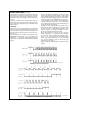
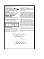
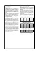
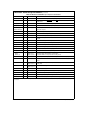
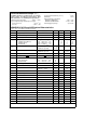
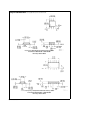
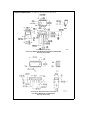
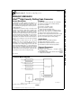
pulses applied to CKI to initialize the part. (See Timing Diagram on pg. 16.) After this initialization, K2 is brought to
supervoltage. K1 is then brought to supervoltage. Now K2 is
brought back to VRW, then K1 is brought back to VRW. The
NM95HS01/02 is now in Write mode.
To program the first byte, set K1 back to supervoltage, and
place the first byte of data (VIH and VIL pulses) onto K2
(starting with the Least Significant Bit). As each bit is placed
on K2, clock the CKI pin to latch the bit. When all bits of the
first byte have been latched in, set K1 to VRW, and poll the
TX output pin for a logic low. This confirms the
NM95HS01/02 has written the byte to memory. Repeat this
sequence to program the remainder of the bytes. When all
13 bytes have been programmed, set K1 and K2 to 0V to
end Write mode.
Programming the NM95HS01/02
The NM95HS01/02 HiSeC Generator uses four pins to read
and write the 13 bytes of on-chip EEPROM. These are the
Key1 (K1), Key2 (K2), TX, and CKI pins. K1 functions as the
chip select line, K2 functions as the data strobe, CKI serves
as the serial clock, and TX acts as the data out pin.
Three voltage levels are required to program the device:
Supervoltage (VSV), Read/Write voltage (VRW), and Ground
(0V). Supervoltage is used to select Read and Write modes
in the device. These modes can only be entered by applying
supervoltage to K1 and K2. This alleviates the risk of the
device entering these modes during normal operation.
The programming protocol for the NM95HS01/02 on-chip
EEPROM array was designed to match National Semiconductor’s MICROWIRE format closely. However, there are
several differences. One is the need to use a supervoltage
to select modes. Another concerns the CKI clock input.
Upon power-up, the NM95HS01/02 CKI input must be
clocked a minimum of 1500 times to ensure the part is ready
for programming. This allows the internal state machines
and registers to perform their necessary power-on sequences. (See Table VII.)
Read Mode
The NM95HS01/02 HiSeC Generator can be placed in
Read mode by applying supervoltage to K1. Upon powerup, both K1 and K2 must be set to VRW, and a minimum of
1500 clock pulses applied to CKI to initialize the part. (See
Timing Diagram on pg. 16.) After this initialization, K1 is
brought to supervoltage. Then K1 is brought back to VRW.
The NM95HS01/02 is now in Read mode.
To read the first byte, set K1 back to supervoltage, and
clock the CKI pin 8 times, while polling TX. EEPROM data is
sent Most Significant Bit first. Continue clocking CKI to read
the remainder of the bytes. When all 13 bytes have been
read, set K1 back to VRW. Set K1 and K2 to 0V to end Read
mode.
Write Mode
The NM95HS01/02 HiSeC Generator can be placed in
Write mode when supervoltage is applied to both K1 and K2
in a specific sequence. Upon power-up, both K1 and K2
must be set to VRW, and a minimum of 1500 clock
Programmer Support for NM95HS01/02
Worldwide third party support is provided by:
Vendor
Contact Number
Xeltek
SuperPro-EM
Universal
Programmer
Europe: 49-5722-203-125 (Germany)
America: 408-524-1929
Asia: 65-296-6433 (Singapore)
BBS: 408-245-7082
National Semiconductor
NM95HS-PRO-X
Americas: 800-272-9959
System General
Turpro-1 Univeral
Device Programmer
Switzerland: 31-921-7844
America: 408-263-6667/800-967-4776
Taiwan: 886-2-917-3015
BBS: 408-262-6438
Hi-Lo ALL-07
Asia: 886-2764-0215
America: 510-623-3850
Evalutation kit support for NM95HS01/02. A demonstration kit for the
HiSeC High Security Rolling Code Generator is available:
National Semiconductor
NM95HSEV
NM95HSPRO
HiSeC Evaluation Board
HiSeC Single Site Programmer
17
http://www.national.com