1
PXZ 19:1A (Find. 1/07)
UNIVERSITI TEKNOLOGI MALAYSIA
DECLARATION OF THESIS / UNDERGRADUATE PROJECT PAPER AND COPYRIGHT
Author's full name :
KOAY JIAN CONG
Date of birth
:
19-12-1988
Title
:
SURFACE MOUNT TECHNOLOGY (SMT)
MICROCONTROLLER BASED RADIO FREQUENCY (RF)
SIGNAL REMOTE LOCATOR
Academic Session:
2010/2011
I declare that this thesis is classified as:
CONFIDENTIAL
(Contains confidential information under the Official Secret
Act 1972)*
RESTRICTED
(Contains restricted information as specified by the
organisation where research was done)*
OPEN ACCESS
I agree that my thesis to be published as online open access
(full text)
acknowledged that Universiti Teknologi Malaysia reserves the right as follows:
1. The thesis is the property of Universiti Teknologi Malaysia.
2. The Library of Universiti Teknologi Malaysia has the right to make copies for the purpose
of research only.
3. The Library has the right to make copies of the thesis for academic exchange.
Certified by :
SIGN TURE Of'SuPERVISOR
881219-07-5035
(NEW
1C NO. /PASSPORT NO.)
Date : MAY 25, 201
NOTES :
EN. KAMAL BIN KHALIL
NAME OF SUPERVISOR
Date: MAY 25, 201
If the thesis is CONFIDENTIAL or RESTRICTED, please attach with the letter from
the organisation with period and reasons for confidentiality or restriction.
"I declare that I have read this thesis and in my opinion this thesis is
sufficient in terms of scope and quality for award a Degree of
Bachelor of Engineering (Electrical - Electronics)."
Signature
Name of Supervisor
: EN. KKMAL BIN KHALIL
Date
: 25 MAY 2011
ii
SURFACE MOUNT TECHNOLOGY (SMT) MIRCROCONTROLLER BASED
RADIO FREQUENCY (RF) SIGNAL REMOTE LOCATOR
KOAY JIAN CONG
Submitted to the Faculty of Electrical Engineering
In partial fulfilment of requirement for the Degree of
Bachelor of Engineering (Electrical – Electronics)
Faculty of Electrical Engineering
Universiti Teknologi Malaysia
MAY 2011
I declare that this thesis entitled "Surface Mount Technology (SMT)
Microcontroller Based Radio Frequency (RF) Signal Remote Locator " is the
results of my own research except as cited in the references. The thesis has
not been accepted for any degree and submitted in candidature of any other
degree.
Signature
Name
: Koay Jian Cong
Date
: 25 MAY 2011
iii
Specially dedicated to:
My father, Koay Hooi Bin
My mother, Vun Fung Yung
My siblings,
Koay Chiao Sin
Koay Jian Hao
Thanks for the loves and supports
iv
ACKNOWLEDGEMENT
First and foremost, I would like to express my heartily gratitude to my
supervisor, En. Kamal bin Khalil for guidance and encouragement given throughout
the progress of this project. Without his guidance and support, this project will not
be completed as well as this thesis.
Moreover, my great appreciation also goes to all my family members and
friends that had been so patient and support me all these years. Without their
encouragement and love, I would not be able to undergo the pressure due to this
project.
During the process of this final year project, I had faced lot of problems
especially come to troubleshooting and idea on how the project can be implemented.
Thanks to my friends, Choo Chian Choong, Voon Zheng Loong, Pui Hing Ngian,
Voon Wee Sun, Gan Chuan Wuu, Sam Xim Min, Ngo Chee Wung, Chee Kok Wai,
Kho Geok Hong and Lam Kong Shen for the advices and idea on my project, finally
I was able to finish my final year project smoothly.
v
ABSTRACT
This thesis with the title of “Surface Mount Technology (SMT)
Microcontroller Based Radio Frequency (RF) Signal Remote Locator” is describing
the system of finding lost items and objects in a very short period of time. It is
briefly describe about how the developing process in order to make this project
success. Besides, the size will be as small as a key chain and would be very
convenient to bring along with the user. This system is a good system where it saves
users precious time. The components that are being used in this project consists of
PIC 16F876A, PIC 16F877A, RF module, LEDs, buzzer and others. The RF modules
can be divided into two. They are the RF transmitter and the RF receiver. When the
product operates, the items or objects that are attached with the remote unit will buzz
and the LED will turn on. This indicates the location of the items and it can be found
in a short period of time.
vi
ABSTRAK
Tesis ini dengan tajuk “Surface Mount Technology (SMT) Microcontroller
Based Radio Frequency (RF) Signal Remote Locator” menggambarkan satu sistem
yang membolehkan pengguna mecari benda atau objek yang hilang dalam masa yang
singkat. Secara singkatnya, tesis ini menggambarkan proses pembangunan supaya
saya berjaya projek ini. Selain daripada itu, saiz produk akan besaiz kecil dan
pengguna akan berasa senang untuk membawanya bersama. Sistem ini adalah sistem
yang bagus kerana ia menjimatkan masa pengguna yang berharga. Komponen yang
diggunakan dalam projek ini terdiri daripada PIC 16F876A, PIC 16F877A, modul
RF, LED, pembunyi dan lain-lain.
Modul RF boleh dibahagikan kepada dua
bahagian, iaitu pemancar RF dan penerima RF. Semasa produk ini beroperasi, benda
atau objek yang dilampiri dengan unit kawalan jarak jauh akan berbunyi dan LED
akan menyala. Ini menunjukkan lokasi benda itu dan ia akan dapat dijumpa dalam
masa yang singkat.
vii
TABLE OF CONTENT
CHAPTER
TITLE
PAGE
THESIS STATUS INFORMATION
SUPERVISOR CONFIRMATION
1
TITLE
i
DECLARATION
ii
DEDICATION
iii
ACKNOWLEDGEMENT
iv
ABSTRACT
v
ABSTRAK
vi
TABLE OF CONTENT
vii
LIST OF FIGURES
xi
LIST OF TABLES
xiv
LIST OF ABBREVIATIONS
xv
LIST OF APPENDICES
xvi
INTRODUCTION
1.1 Background of Study
1
1.2 Objectives
2
1.3 Problem Statement
3
1.4 Scope of the Study
4
viii
2
LITERATURE REVIEW
2.1 Book’s Review
2.1.1
Myke Predko, “Programming and
Customizing the PIC Microcontroller”
2.2 Jornal’s Review
2.2.1
5
5
6
Peter J. Boden, “Surface Mount
Technology – A Study of Safety
Considerations: Silver Migration and
Adhesive Flammability”
2.2.2
6
Steve Yessa, “Microcontroller-Based
Remote Locator Using Asynchronous
Serial Communication”
2.2.3
Lawrence D. Rosenthal, “Paired Lost Item
Finding System”
2.3 Thesis’s Review
2.3.1
7
10
15
Suhaila binti Mohd. Najib,
“Microcontroller Based Remote Locator
Using Radio Frequency Signal”
3
15
METHODOLOGY
3.1 Methodology Flow
3.1.1
18
Gantt Chart
19
3.2 Hardware Overview
20
3.2.1
Methodology Overview
20
3.2.2
PIC 16F876A-I/SO
21
3.2.3
PIC 16F877A-I/PT
22
3.2.4
Clock Generator
23
3.2.5
MCLR Pin
24
3.2.6
USART Configuration
25
3.2.7
USART Baud Rate Generator (BRG)
26
ix
3.2.8
USART Asynchronous Mode
26
3.2.9
USART Asynchronous Transmitter
27
3.2.10 USART Asynchronous Receiver
28
3.2.11 RF Module
29
3.2.12 Transmitter RF-TX-433
29
3.2.13 Receiver RF-RX-433
30
3.2.14 Sounder
31
3.2.15 USB ICSP PIC Programmer
32
3.3 Programming Software Overview
32
3.3.1
Introduction to Programming Software
33
3.3.2
PIC Language
33
3.3.3
MPLAB IDE Assembler
34
3.3.4
Create and Build Project
35
3.4 Designing Software Overview
36
3.4.1
Create a New PCB Project
37
3.4.2
Create a New Schematic Sheet
38
3.4.3
Setting the Schematic Document Options
38
3.4.4
Locating Components and Loading the
Libraries
39
3.4.5
Placing the Components on Schematic
40
3.4.6
Wiring Up the Circuit
40
3.4.7
Nets and Net Labels
41
3.4.8
Compiling the Project to Check for Errors
41
3.4.9
Creating a New PCB
42
3.4.10 Transferring the Design
43
3.4.11 Ready to Start the PCB Design Process
43
3.4.12 Setting Up the PCB Workspace
44
3.4.13 Component positioning and Placement
Options
44
3.4.14 Setting Up the Design Rules
44
3.4.15 Positioning the Components on the PCB
45
3.4.16 Routing the Board
46
3.4.17 Verifying the Board Design
47
x
4
5
6
PROJECT IMPLEMENTATION
4.1 Introduction
48
4.2 The Control Unit (CU)
48
4.3 The Remote Unit (RU)
49
4.4 Transmitting and Receiving Flowchart
50
4.5 PIC Interfacing
51
4.6 PCB Board Interface
53
4.7 Programming Coding
55
RESULTS
5.1 Control Unit (CU)
57
5.2 Remote Unit (RU)
58
5.3 Remote Locator Capability
59
Conclusion
6.1 Introduction
60
6.2 Problems
61
6.3 Project Improvement
61
REFERENCES
62
APPENDIX
64
xi
LIST OF FIGURES
No.
TITLE
PAGE
2.1
Base unit system diagram
8
2.2
Flow chart for the main menu
8
2.3
UART signal packing and unpacking
9
2.4
Unpacked remote asynchronous signal
9
2.5
Perspective view of a lost item locator
10
2.6
Paired locators finding lost item
11
2.7
Simplified schematic diagram
11
2.8
Flow chart part 1
13
2.9
Flow chart part 2
13
2.10
Flow chart part 3
14
2.11
Flow chart part 4
14
2.12
Block diagram of the remote locator
14
2.13
Transmitter block diagram
15
2.14
Receiver block diagram
16
2.15
Asynchronous transmitter bitmap
16
2.16
Asynchronous receiver bitmap
17
3.1
Methodology flow
18
3.2
Functional block diagram
21
3.3
Pin diagram of PIC 16F876A
21
3.4
PIC 16F876A-I/SO
21
3.5
Pin diagram of PIC 16F877A
22
3.6
PIC 16F877A-I/PT
22
xii
3.7
Crystal connection
24
3.8
MCLR pin connection
25
3.9
NRZ format
27
3.10
Simplified transmission block diagram
27
3.11
Simplified reception block diagram
28
3.12
Combinational block diagram
28
3.13
RF transmitter module
30
3.14
RF receiver module
30
3.15
PCB-mount buzzer
31
3.16
Programmer
32
3.17
Male pin
32
3.18
MPLAB IDE assembler
34
3.19
PICkit 2
35
3.20
PICkit 2 user interface
36
3.21
Altium Designer Summer 09
37
3.22
Libraries search window
39
3.23
Components that had being transferred to PCB
43
3.24
Arranged components
46
3.25
Design rule verification report
47
4.1
Control unit block diagram
49
4.2
Remote unit block diagram
49
4.3
Transmitting process flowchart
50
4.4
Receiving process flowchart
50
4.5
Transmitter schematic diagram
52
4.6
Receiver schematic diagram
53
4.7
Transmitter PCB Layout
54
4.8
Receiver PCB Layout
54
4.9
Transmitter PCB board
54
4.10
Receiver PCB board
54
4.11
Transmitter coding
55
4.12
Receiver coding
55
xiii
5.1
Transmitter PCB board
58
5.2
Receiver PCB board
58
xiv
LIST OF TABLES
No.
TITLE
PAGE
3.1
FYP 1
19
3.2
FYP 2
19
3.3
Capacitor selection for crystal oscillator
23
3.4
FOSC and desired baud rate
26
5.1
Remote locator capability
59
xv
LIST OF ABBREVIATIONS
BRG
-
Baud Rate Generator
CU
-
Control Unit
LED
-
Light Emitter Diode
PCB
-
Printed Circuit Board
PIC
-
Programmable Interface Controller
RF
-
Radio Frequency
RU
-
Remote Unit
RX
-
Receiver
SMT
-
Surface Mount Technology
TX
-
Transmitter
xvi
LIST OF APPENDICES
APPENDIX
TITLE
PAGE
A
Transmitter’s coding
64
B
Receiver’s coding
68
1
CHAPTER 1
INTRODUCTION
1.1
Background of Study
The title of this project “Surface Mount Technology (SMT) Microcontroller
Based Radio Frequency (RF) Signal Remote Locator” can basically being divided
into 3 parts. They are the SMT microcontroller, radio frequency signal and remote
locator. Before the project was started, the definition of the parts had to be defined.
SMT microcontroller is a shirking version of the through-hole technology
microcontroller. From online definition directory, SMT is a method for constructing
electronic circuits in which the components are mounted directly onto the surface of
printed circuit boards (PCB). The size can be one-quarter to one-tenth the size and
weight of the microcontroller [6].
The second part is the RF signal. Another name for RF is radio waves. It is a
subset of electromagnetic radiation. The wavelength of RF can be ranged from 1
mm to 100 km, while the frequency ranged from 30 kHz to 300 GHz
[7]
. Since RF
signal can travel within a distance of a house, hence, it had being chosen as the
communication method of the remote locator. The frequency of the RF signal is
being determined from the formulae below [8].
2
Remote locator is the final product of this project. What is remote locator?
Remote locator is a control locator that will locate the position of the household
items. Since the locator can be controlled remotely, so, it can functions on the items
located far away where the items are in the searching frequency range of the RF
signal.
The final product will help most on the people in Malaysia that are frustrated
by searching missing household items.
1.2
Objectives
Although in other country, remote locators were manufactured widely,
however, in Malaysia, remote locator that is using surface mount technology
microcontroller had not being manufactured by any industries. Hence, this project is
being developed to build the remote locator that will locate household items easily by
just a push on the button.
There are 4 objectives that lead to the research of this project. The first
objective is to minimize the size of the circuit built by using SMT microcontroller.
With this technology, the remote locator can be assembled into the size of a keychain.
So, it can be attached to small household items.
In order to produce the final product, the communication method is the vital
factor.
Hence, the second objective of this project is to develop 2 or more
3
communication systems between microcontrollers using radio frequency (RF)
module.
The third objective is to benefit the people who always dislocate their
household items such as keys, spectacles, and etc. The remote locator will locate the
devices without searching. It will represent by loud distinctive sound and LED that
will be blinking with a bright light.
Last but not least, the fourth objective is to save users‟ time. In order to
search those dislocate household items, lots of time will be spent. Time is precious.
So, with the aid of a remote locator, missing items will be found within a short
period of time.
The target users of this product are varies. They can be housewives, students,
old folks, and etc. Since it is user-friendly, small and light, hence, the product will
be used widely soon. Other than that, the cost will be cheaper if it is manufactured in
our own country.
1.3
Problem Statement
The problem that leads to this study is the household items are missing due to
the dislocation of users.
In order to solve the problem stated, the project with the title of “Surface
Mount Technology (SMT) Microcontroller Based Radio Frequency (RF) Signal
Remote Locator” was being carried out. The purpose of it is to find out those
dislocate household items within a short period of time.
4
1.4
Scope of Study
The scopes of study of this project are to focus on the radio frequency (RF)
module that will be used as the main communication method, the communication
between transmitter and receiver, the product will be build by using SMT
microcontroller and SMT peripheral components, and to make it operate by using
high level programming language for example the C code using MPLAB.
5
CHAPTER 2
LITERATURE REVIEW
2.1
Books’ Review
Book‟s review is the summarize work that is done by referring to the
hardcopy of a book that might be in the form of magazines, encyclopaedias, and
others.
2.1.1
Myke Predko, “Programming and Customizing the PIC
Microcontroller”
The book from Myke Predko, “Programming and Customizing the PIC
Microcontroller” is a good material for the literature review. This book is basically
focus on PIC families and the applications of the microcontroller.
The programming languages that are used in this book are assembly language,
basic and C [1].
6
The contents of the book include the method to setting up your own PIC
microcontroller, PIC microcontroller interfacing capabilities, and application, the
basic electronics, the digital electronics, and some useful circuits and routines, such
as the LED blinking circuit, and LCD display circuit.
This book is very useful because it can aid me with the programming
language and also the circuit building.
Besides, the data sheets of the
microcontrollers are being included in this book.
2.2
Journals’ Review
Journal‟s review is summarizing the related points from the research that
others had done.
2.2.1
Peter J. Boden, “Surface Mount Technology – A Study of
Safety Considerations: Silver Migration and Adhesive
Flammability”
This work represents original application of silver migration and flammability
testing for evaluating surface mount device (SMD) silver electrodes and surface
mount adhesives.
According to the writer Peter J. Boden, “The migration of silver can result in
reduced spacing between poles of opposite polarity and ultimately, to a short circuit.
Besides of that, silver migration is an electrochemical process whereby silver, in
7
contact with an insulating material in a humid environment and under an applied
electric field, leaves its initial location in ionic form and redeposit at another location.
This may lead to a reduction in electrical spacing or ultimately to a short circuit [2]. ”
Hence, silver migration is a critical problem that arises during the SMT being
used on the SMD.
There are many factors that will lead to silver migration.
According to this thesis, the factors include, an increase in the applied potential, an
increase in the time of the applied potential, an increase in the level of relative
humidity (RH), an increase in the presence of ionic and hygroscopic contaminants on
the surface of the substrate and a decrease in the distance between electrodes of
opposite polarity [2].
Moreover, there are various methods that can prevent the occurrence
of the silver migration. The first method stated in the journal is by alloying the silver
with an anodically stable metal such as palladium. The second method is the use of a
hydrophobic coating over the PWB to shield its surface from humidity and ionic
contaminants. The third method is by plating the silver with metals such as tin,
nickel, or gold [2].
2.2.2
Steve Yessa, “Microcontroller-Based Remote Locator Using
Asynchronous Serial Communication”
According to the journal written by Steve Yessa, “the goal of the project is to
develop a remote locator device that is used to find lost items by sending a RF signal
to small remote units attached to various items in the home. The names of the lost
items are found in a list of saved names and are selected for location. The remote
unit attached to the desired item receives the RF transmitted digital ID code from the
base unit and produces an audible alert tone to allow the user to locate the items. In
this journal, the base unit is microcontroller based and interfaces with an LCD screen
8
and a keypad. The user menu is displayed on the LCD and allows three different
modes of operation: save mode, alert mode, and load mode [4]. ”
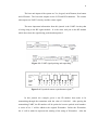
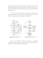
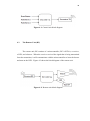
Figure 2.1: Base unit system diagram [4]
Figure 2.2: Flow chart for the main menu [4]
Figure 2.1 shows the base unit systems with the keypad communicate with
the microcontroller and it display the modes of operation on the LCD screen and 3
modes will be available for the users. After that, the signal will be transmitted
through the RF transmitter and will be receive by the RF receiver. Figure 2.2 shows
the operational flow chart of the main menu.
9
The base unit inputs of the system are Vcc, keypad, on/off button, alert button
and off button. The base unit outputs are the LCD and RF transmitter. The remote
unit outputs are UART circuitry and the remote signal.
The most important information from this journal is the UART circuitry that
is being using in the RF signal module. It is the most vital part in the RF module
which show how the signal being packed and unpacked.
Figure 2.3: UART signal packing and unpacking [4]
Figure 2.4: Unpacked remote asynchronous signal [4]
In this journal, the example given is the ID number that needs to be
transmitting through the transmitter with the value of 11001010. After passing the
transmitting UART, the ID number will be packed to become packed serial number.
A series of bit „1‟ will be added to the original ID number. Before the ID number,
bit „0‟ will be added to represent the starting of the string of ID number. After the
10
string of ID number, 2 bits of „1‟ will be added. After the ID number is being packed,
it will be send through the RF transmitter can being transmitter.
The transmitted signal from the transmitter will be received by the receiver
and pass through the same UART circuitry as the transmitter. Hence, it will start to
unpack the packed serial number. The UART circuitry will detect the first bit which
change from bit „1‟ to bit „0‟. After the first bit „0‟, the string of number will be
taken as the original ID number. The last 2 bit „1‟ will be ignored and the serial
number is successfully being unpacked [4].
These types of UART signal packing and unpacking will being used as a
good reference for my project.
2.2.3
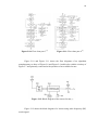
Lawrence D. Rosenthal, “Paired Lost Item Finding System”
This journal is more alike to mine. The final product shape and size is the
conceptual shape and size of my project.
Figure 2.5: Perspective view of a lost item locator
11
Figure 2.6: Paired locators finding lost items
Figure 2.5 shows the perspective view of the lost item locator, while Figure
2.6 shows a schematic representation of the operation of the paired locators for
finding one of them attached to the lost items.
There are 2 parts of hardware needed. They are the remote unit and the
control unit. The remote unit is attached to the household items such as a key. In
Figure 2.6, when a finger is press on the button on the control unit, the receiver on
the remote unit will receive the signal and generate a loud distinctive audible sound
and also the blinking of LED which represent the signal had being received.
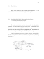
Figure 2.7: Simplified schematic diagram [3]
12
Figure 2.7 shows the simplified schematic diagram of the electronic circuitry
usable with a buzzer.
According to the journal, the explanation of the circuit shows above is as
below. “Two serially connected 3V batteries form a DC power supply that provides
a voltage to the microcontroller. The microprocessor was designed to operate from a
DC power source providing between 3V and 5.5V. In order to provide a voltage in
the middle of the operating range, the LED at position 20 drops the 6V to 4V [3]. ”
Next, the operation method will be reviewed. “In sleep mode, the
microprocessor consumes only about 1 µA of current while in active mode, it
consumes about 1 mA of current. The remote unit will stay in sleep mode until
button 22 is activated. The microprocessor has 3 outputs, which are OUT-1, OUT-2,
and OUT-3 [3]. ”
“The first output OUT-1 was connected to a load resistor that is connected to
the ground.
When the first output OUT-1 goes high, current flows out of the
microprocessor through that output, and corresponding additional current flows into
the microprocessor power input Vcc through the LED causing it to emit additional
light. The second output OUT-2 is connected to the inputs of both a buffer at
location 46 and an inverting tri-state buffer at location 48, both of which may be
formed from a quad tri-state buffer and a resistor. The buffer simply outputs a highpower signal corresponding to its low-power input while the inverting tri-state buffer
either outputs a high-power signal inverted from its low-power input or presents a
high-power signal inverted from its low-power input or presents a high-impedance
output depending upon the signal from the third output OUT-3 from the
microprocessor. A piezoelectric audio transducer at position 50 is connected across
the outputs of the buffer and the inverting tri-state buffer [3]. ”
“Assuming that the microprocessor has activated the inverting tri-state buffer
with its third output OUT-3, the outputs of the two buffers are complementary, either
0V or 6V, with the polarity determined by the signal from the microprocessor‟s
second output OUT-2. The bipolar signal driving the transducer at position 50
13
generates a louder audio signal as the piezoelectric unit is driven in both directions.
For audio signaling, this output OUT-2 is switched at a frequency in the range of 5.5
kHz to 7.5 kHz, with the effect that the audio transducer emits an audio signal in this
frequency range [3]. ”
The above operation of the transmitter circuit will be a good reference to
make my project success. Some flow chart from the thesis can be used as a good
reference for the operation of my final product, the remote locator.
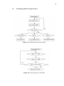
Figure 2.8: Flow chart part 1[3]
Figure 2.9: Flow chart part 2 [3]
Figure 2.8 and Figure 2.9 shows flow diagram of an algorithm
complementary to those of Figure 2.6 and primarily concerned with the operation of
a lost locator receiving a search signal and the responds.
14
Figure 2.10: Flow chart part 3 [3]
Figure 2.11: Flow chart part 4 [3]
Figure 2.10 and Figure 2.11 shows the flow diagrams of an algorithm
complementary to those of Figure 2.8 and Figure 2.9 usable also with the circuitry of
Figure 2.7 and primarily concerned with operation of an available locator.
Figure 2.12: Block diagram of the remote locator [3]
Figure 2.12 shows the block diagram of a locator using radio frequency (RF)
search signal.
15
2.3
Thesis’ Review
Thesis review can be in the form of online source of hardcopy. It is the
summarization from the research that had being done before by others.
2.3.1
Suhaila binti Mohd. Najib, “Microcontroller Based Remote
Locator Using Radio Frequency Signal”
The project in this thesis used the microcontroller with through-hole
technology. So, I am to reduce the size of the remote locator. In addition, this thesis
discuss on the remote locator using RF. In the hardware design, the board can be
divided into two parts which are Control Unit and Remote Unit. The transmitter and
the receiver that implemented RF signal are USART Asynchronous type.
USART Asynchronous type has just a little bit difference between UART.
The “S” means synchronous. However, in this thesis, the synchronous key had being
deactivated [5].
Figure 2.13: Transmitter block diagram [5]
16
Figure 2.14: Receiver block diagram [5]
Figure 2.13 and Figure 2.14 shows the transmitter block diagram and receiver
block diagram respectively. Every UART or USART circuitry has its own module.
Figure 2.15: Asynchronous transmitter bitmap [5]
17
Figure 2.16: Asynchronous receiver bitmap [5]
18
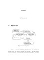
CHAPTER 3
METHODOLOGY
3.1
Methodology Flow
Figure 3.1: Methodology flow
Figure 3.1 shows the methodology flow that starts from research and
literature review and follow by discussing with supervisor.
After that, suitable
components are being selected and SMT implementation will be done. After SMT
19
implementation, RF will be implemented. After the implementation of RF module,
the PICs are being programme and at the final stage, testing and analysis will be
done. The final part of the whole project is to the process of results‟ documentation.
3.1.1
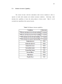
Gantt Chart
Table 3.1: FYP 1
Table 3.2: FYP 2
20
3.2
Hardware Overview
In this section, the hardware which consists of components will be discussed
and explained.
3.2.1
Methodology Overview
The chosen SMT PICs are the PIC 16F876A SOIC package and PIC
16F877A TQFP package. SOIC stands for small-outline integrated circuit while
TQFP is thin quad flat pack. The circuits‟ layout will be drawn by using the software,
Altium Designer Summer 09 that is available in the PCB lab in UTM.
After that, the PCB layout will also be drawn. The circuit will be printed on
the PCB board and soldering work need to be carried out. As a result of it, the circuit
will be successfully built.
The hardware can be divided into 2 parts. They are the control unit (CU) and
the remote unit (RU). SMT is being implemented into both of the units. LCD will
be used if it is needed. In my project, I am required to build one CU and a few RU.
Inside the RUs, SMT buzzer or audio transducer will be implemented.
The communication between hardware can be done by the implementation of
the RF module. Transmitter will be implemented into the CU while receiver will be
implemented into the RUs.
21
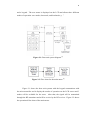
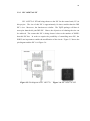
Figure 3.2: Functional block diagram
Figure 3.2 shows the operational block diagram of the remote locator which I
wish to build.
3.2.2
PIC 16F876A-I/ SO
PIC 16F876A-I/ SO is a surface mount PIC. Although the size is smaller
than the Dual-In Line (DIP) PIC, however, the functions and the pins are similar. It
was being implemented in this project as the PIC of the remote unit (RU) is because
it is a common PIC. In addition, the size of this PIC is small and the purpose to
reduce the size of the RU can be achieved. Besides, the PORTs on the PIC are
adequate for the buzzer and LEDs implementation.
Figure 3.3 shows the pin
diagram for this PIC while Figure 3.4 shows the PIC.
Figure 3.3: Pin diagram of PIC 16F876A
Figure 3.4: PIC 16F876A-I/SO
22
3.2.3
PIC 16F877A-I/ PT
PIC 16F877A-I/ PT had being chosen as the PIC for the control unit (CU) in
this project. The size of this PIC is approximately 10 times smaller than the DIP
PIC‟s size. Moreover, the functions are similar. The TQFP package will have 4
more pins than the 40 pins DIP PIC. Hence, the objectives of reducing the size can
be achieved. The reason this PIC is being chosen is due to the number of PORTs
that this PIC has. In order to acquire the possibility of controlling more RU, the
PORTs are important to enable the modification of the circuit. Figure 3.5 shows the
pin diagram and the PIC is in Figure 3.6.
Figure 3.5: Pin diagram of PIC 16F877A
Figure 3.6: PIC 16F877A-I/PT
23
3.2.4
Clock Generator
The clock of a PIC microcontroller need to be generates. In order to generate
clock for the PIC, four available methods can be used. These different options are
designed based on different specifications and requirements.
Cost, speed and
accuracy are the three most important elements when choosing the clocking methods.
With small quantities, the cost differences are small. However, for large quantities, it
would be prudent to select the lowest clock frequency that comfortably meets the
application requirements as the cost savings increase with quantity.
In order to
generate the correct results from the PIC, the clock‟s speed is vital. The PIC may not
be functioning when the values of the clock generators are wrongly used. The last
element which is the accuracy is highly related to the timing of the clock generator [9].
Table 3.3 shows the capacitor selection for crystal oscillator.
Table 3.3: Capacitor selection for crystal oscillator [9]
The four clock generator or crystals that are available in the market consist of
RC oscillator (resistor / capacitor), XT oscillator (crystal / ceramic resonator), HS
oscillator (high speed crystal / ceramic resonator) and LP oscillator (low power
crystal) [9].
Among these four methods, RC is the least accurate method. However, when
timing is not a critical concern, this method can be used. In this project, HS which
24
the operating frequency is up to 20MHz had been used. The crystal will oscillate at a
fixed frequency, which is 50ppm (parts per million) for 20MHz crystal [5]. This will
allow the hardware timer to measure the exact time intervals and to produce accurate
output signal. Figure 3.7 shows the connection of the crystal with two capacitors.
Theoretically, the capacitors that are connected to the crystal will assure the stability
of the oscillation. However, practically, without the capacitors, the circuits are
functioning better.
Figure 3.7: Crystal connection
3.2.5
MCLR Pin
MCLR pin acts as the reset pin, which is also known as a “behavior
controller” for a PIC
[5]
. In order to trigger a PIC into the known condition, the
MCLR pin has to be activates by connecting a pull-up resistor (10kΩ) with the Vdd
(5V) and ground (0V). MCLR pin for PIC 16F876A-I/ SO is located at pin 1 while
for PIC 16F877A-I/PT, MCLR pin is located at pin 18. For the controller, a switch
can be connected to the MCLR in order to interrupt the program for the purpose of
program execution. When the reset button is being pushed, all the registers will
return to the starting condition. Figure 3.8 shows the MCLR pin connection.
25
Figure 3.8: MCLR pin connection
3.2.6
USART Configuration
Universal Asynchronous Receiver Transmitter (UART) is a piece of
computer hardware that translates data between parallel and serial forms.
The
universal designation indicates that the data format and transmission speeds are
configurable and that the actual electric signaling levels and methods typically are
handled by a special driver circuit external to the UART.
Hence, many PIC
microcontrollers had integrated with this device and it is called USART
[11]
.
Universal Synchronous Asynchronous Receiver Transmitter (USART) allows the
interface between PIC microcontroller and serial devices or synchronous serial
device.
USART can be configured asynchronous full-duplex device, as a
synchronous half-duplex master, or as a synchronous half-duplex slave.
Asynchronous mode is used mostly in communication between analog-to-digital and
digital-to-analog for serial EEPROM interfacing. [5]
26
3.2.7
USART Baud Rate Generator (BRG)
The USART supports a wide range of software programmable baud rates and
data formats and in either Synchronous or Asynchronous mode [10]. In Asynchronous
mode, bit BRGH (TXSTA <2>) controls the baud rate while the SPBRG register
controls the period of a free running 8-bit timer. Writing a new value to the SPBRG
register causes the BRG timer to be reset (or cleared). This ensures the BRG does
not wait for a timer overflow before outputting the new baud rate
[12]
. In order to
generate the baud rate, formula in Table 3.4 with the give FOSC and desired baud
rate that the user desired to use.
Table 3.4: FOSC and desired baud rate [12]
3.2.8
USART Asynchronous Mode
In this project, the Asynchronous mode will be used. In this mode, nonreturn-tozero (NRZ) format is being used. In NRZ, the positive voltage will be
represented by 1‟s while the negative voltage will be represented by 0‟s. NRZ
format normally operating in 10 bits where the start bit is sent as a logic low bit;
while the stop bit is sent as a logic high bit.
Hence, there is always a clear
demarcation between the previous character and the next one
[14]
. Figure 3.9 shows
the NRZ format of the USART Asynchronous mode. In this project, four important
elements that will be considered consist of baud rate generator, sampling circuit,
transmitter and receiver [13].
27
Figure 3.9: NRZ format
3.2.9
USART Asynchronous Transmitter
In the USART Asynchronous mode, the controlling for the transmission is
mainly operated by the TXSTA register [14]. In this project, eight bits of data will be
transferred. Hence, the programme needs to enable the TX9 bit. Once this bit has
been set, the initialization of the register will enable and cause a transmission. The
TX9 bit will enable the transmitter to send eight or nine bits of data after the starting
bit. Figure 2.13 and Figure 2.15 in Chapter 2 had shown the block diagram and the
Bitmap respectively.
Figure 3.10 will show the simplified transmission block
diagram.
Figure 3.10: Simplified transmission block diagram [10]
28
3.2.10 USART Asynchronous Receiver
In the USART Asynchronous mode, the controlling for the reception is being
mainly operated by the RCSTA register
[14]
.
In the transmission part, we had
initialized the transmitter to transmit 10 bit data. Hence, in the reception part, the
RX9 bit will be activated in order to receive eight or nine bits after the detection of a
start bit. Figure 2.14 and Figure 2.16 in Chapter 2 had shown the block diagram and
the Bitmap respectively. The simplified reception block diagram will be show in
Figure 3.11.
Figure 3.11: Simplified reception block diagram [10]
Figure 3.12: Combinational block diagram [10]
29
Figure 3.12 shows the final combination of all the parts that had being
discussed and the signalling of the transmitter and the receiver of an USART are
shown in the block diagram above.
3.2.11 RF Module
In the beginning of Chapter, the phrase radio frequency had being pin-pointed.
So, radio frequency module is an important element in the project.
Today
technologies in the field of mobile communication systems are becoming more and
more common and user-friendly.
Hence, many low cost radio frequency (RF)
modules are available in the market.
In this project, the RF modules that are
manufactured by Cytron Technologies are being implemented. The consideration on
buying a module rather than build it is due to the cost of building a module is more
expensive than a ready-built module. The modules are ready to plug into the circuit
to interface with the PIC and complete the communication system.
The RF module that used in this project is at the frequency of 433 MHz.
According to ISM band, 433 MHz if in licensed free frequency range. ISM band
means industrial, scientific and medical radio bands which it is reserved for
international uses of RF electromagnetic fields in that area other than communication
[15]
.
3.2.12 Transmitter RF-TX-433
Figure 3.13 shows the RF transmitter module that will be implemented.
30
Figure 3.13: RF transmitter module [16]
3.2.13 Receiver RF-RX-433
Figure 3.14 shows the receiver module that will be implemented .
Figure 3.14: RF receiver module [17]
31
3.2.14 Sounder
Figure 3.15: PCB-mount buzzer [18]
Figure 3.15 shows the PCB-mount buzzer. The specification of the buzzer is
as below.
Rated Voltage: 2. 0~6.0VDC
Rated Current: ≤ 40mA
Sound Output: ≥ 85DB
Resonant Frequency: 2400HZ
This buzzer will be implemented in my project due to its size and it is not a
piezo type buzzer that will have a fix frequency at 2.4 KHz although the frequency is
changed.
32
3.2.15 USB ICSP PIC Programmer
Figure 3.16: Programmer [19]
Figure 3.17: Male pin
Figure 3.16 and Figure 3.17 shows the programmer that will be used in order
to programme the surface mount PIC. A SMT PIC will not be able to suit the size of
an UIC-S. Hence, the Male Pin in Figure 3.17 is being used to replace UIC-S. A
circuit from the SMT PIC will be built. After the interface between UIC00A and the
Male Pin is built, the programming to the SMT PIC can be done.
3.3
Programming Software Overview
In programming software parts, MPLAB and PICkit 2 is being utilized to
write the code, build a project and to program the PIC microcontrollers.
33
3.3.1
Introduction to Programming Software
Programme the PIC is a tough task in develop an embedded system that
ensure that the system work as expected. In order to programme the PIC, it is a must
to use assembler software.
Assembler software is software that converts the
instructions into a pattern of bits that the PIC can understand and do its job. This
pattern bits is called machine language
[20]
. This software will also generate many
files but one of the important file is .hex file. This file will be used by PIC to do its
job.
In order to load the .hex file, programmer and emulator are needed.
Programmer function as to a hardware device that configures programmable nonvolatile circuits such as EPROMs, EEPROMs, Flashs, PALs, FPGAs or
programmable logic circuits.
Meanwhile, a simulator is a tool that helps the
assembler to load the .hex file into the PIC. [5]
3.3.2
PIC Language
Language is the source of communication among human beings. Different
countries have different languages. It is similar to the communication happens in the
PIC. Language that is use must be understood by the PIC. There are two major
types of programming languages which are low level languages and high level
languages. Low level languages are further divided into machine language and
assembly language. Examples of high level language are C, C++, micro code and
Basic. For this project, C language will be used in order to program the PIC
[5]
. The
advantages of high level language enable us to write programme by using words and
mathematical symbols rather than mnemonic code. The advantages of using high
level language are user-friendly, similar to English with vocabulary of words and
symbols, easier to learn and maintain, shorten the time to programme, program
written in a high-level language can be translated into many machine language and
34
therefore can run on any computer for which there exists an appropriate translator
and it is independent of the machine on which it is used.
3.3.3
MPLAB IDE Assembler
Figure 3.18: MPLAB IDE assembler
Assembler is a programming language that is part of the toolset used in
embedded systems programming. It comes with its own distinct set of rules and
techniques.
It is essential to adopt and learn IDE (Integrated Development
Environment) when developing programs. MPLAB IDE is an excellent tool for PIC
microcontrollers, both for learners and professionals. In addition, it is easy to get and
it is an open source for public. The main software tools and files created and used by
MPLAB during the development process
[21]
are the text editor which is used to
create and modify source code text file, the assembler which create .hex file, the
simulator the allows program to be tested in software before downloading and the
programmer which enable the downloads of machine code into a chip.
35
3.3.4
Create and Build Project
The MPLABD IDE is software which is very common and it is being used
widely in the field of engineering. There are several steps to be followed in order to
create and build a project.
1.
Open MPLAB IDE application. We can choose our desired PIC by clicking
Configure > Select device > Choose. After the PIC is being chosen, click
OK.
2.
In order to build a project, a project wizard had to be created by Project >
Project Wizard. When a project wizard interface shown up, Next is being
clicked twice. These steps determine the active toolsuit that are being used
by the user. For example the C language and Hi-Tech Universal Toolsuite.
3.
Next, browse the project path and click Next > Finish in order to enable the
typing of a programme. When New is clicked, a black workspace will be pop
up and the coding can be written in it.
4.
After that, save the programming as file .c. After the .c file is being saved, a
source file must be included in order to build the code.
5.
Click on Project > Build on the toolbar and the result will be generated.
Besides, a .hex file will also be generated from this step of procedure.
6.
After a project is being successfully built, PICkit 2 is used to load .hex file
into the PIC. Figure 3.19 shows the icon of PICkit 2.
Figure 3.19: PICkit 2
7.
In order to load the program, click on File > Import Hex and then choose
the .hex file.
36
8.
Then, click Write > Verify and a microcontroller is being successfully
programmed. Figure 3.20 shows the PICkit 2 user interface.
Figure 3.20: PICkit2 user interface
3.4
Designing Software Overview
Altium Designer Summer 09 is being used to draw the circuits outline,
connection and the PCB board layout. This is not a common software and a step by
step guide will be discussed for a better understanding of the interface, information
37
on how to use panels and managing design documents. Figure 3.21 shows the
software application icon.
Figure 3.21: Altium Designer Summer 09 [22]
3.4.1
Creating a New PCB Project
To create a new PCB project, following steps is being taken.
1.
Select File > New > Project > PCB Project from the menus.
2.
The project panel will open, displaying the new project file,
PCB_Project1.PrjPCD with no document added.
3.
Rename the new project and save the project by selecting File > Save
Project As. Browse the location for the project and click Save.
38
3.4.2
Creating a New Schematic Sheet
Every design starts with the schematic diagram. Hence, before we are able to
create the PCB drawing, a schematic diagram is needed to be drawn. To create a
new schematic sheet, following steps is being taken.
1.
Right-click on the project file in the projects panel and select Add New to
Project > Schematic. A blank schematic sheet named Sheet1.SchDoc will be
open.
2.
Rename and save the new schematic by selecting File > Save As. The path of
saving the new schematic should be the same as the PCB project.
3.
Right-click on the project filename in the projects panel and select Save to
save the project.
3.4.3
Setting the Schematic Document Options
The first thing to do before the drawing of a circuit is started is to set up
appropriate document options. The following steps need to be followed.
1.
From menus, select Design > Document Options.
2.
We can change the requirement of the options for example the sheet size of
the paper and many other options.
3.
Click OK to update the changes made.
4.
In order to make the document fill the viewing area, select View > Fit
Document.
5.
Click File > Save to save the schematic sheet.
39
3.4.4
Locating Components and Loading the Libraries
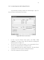
A powerful library searching is capable in the Altium Designer. Figure 3.22
shows the Libraries Search window of the software.
Figure 3.22: Libraries search window
1.
In order to open the Libraries Search window, select Tools > Find
Component. The setting of Scope, Path, File Mask and everything must
follow the options as in Figure 3.22.
2.
The Field row is set to Name, the Operator is set to contain and the Value is
the name of the components that we would like to search.
3.
Click the Search button after the setting is being done. The Query Results
are displayed in the Libraries panel as searching still continued.
4.
Click on the component to select the component.
40
3.4.5
Placing the Components on Schematic
1.
Select View > Fit Document.
2.
Display the Libraries panel by clicking on its tab on the right of the
workspace.
3.
Select the Miscellaneous Devices. IntLib library from the Libraries dropdown list at the top of the Libraries panel to make is the active library.
4.
Search the components and click on the component to select it, and then click
the Place button, or just double-click on the component name.
The
component that floating on the cursor can be rotate by pressing X (flip
horizontally), Y (flip vertically), Spacebar (rotate 90 degree anti-clockwise)
and Shift + Spacebar (rotate 90 degree clockwise) and right-click to place the
component.
5.
The properties of the components can be shown by double-click the
component that had being placed on the schematic diagram.
3.4.6
Wiring up the circuit
Wiring is the process of creating connectivity between various components of
the circuit. To wire up the schematic, following steps are required to be completed.
1.
Wire up the components by select
Place > Wire and connect the
components following the design.
2.
Right-click on the workspace is to make a corner or to connect the
components with wires.
3.
Press Esc in order to stop the process of wiring.
41
3.4.7
Nets and Net Labels
Each set of component pins that we have connected to each other now form
what is referred to as net.
1.
Select Place > Net Label. A net label will appear floating on the cursor.
2.
Press TAB to edit the label before placing it.
3.
Type the desired name in the Net field, and then click OK to close the dialog.
4.
When we place the net label, the cursor will change to a red cross when the
net label touches the wire and light gray when a pin is being label instead of a
wire.
5.
After finish labelling, select File > Save to save the circuit.
6.
Finally, checking the electrical properties of the schematic in order to verify
the design by selecting Project > Project Options and setting up the Error
Reporting, Connection Matrix and Comparator tabs.
3.4.8
Compiling the Project to Check for Errors
Compiling a project checks for drafting and electrical rules errors in the
design documents and details all warnings and errors in the message panel, and gives
detailed information in the Compiled errors panel.
1.
To compile a project, select Project > Compile PCB Project.
2.
When the project is compiled, all warning and errors will be displayed in
Messages panel. Check for the errors occurred and fix all the errors out in
order to enable the creation of a new PCB.
42
3.4.9
Creating a New PCB
Before a design is being transferred from the Schematic Editor to the PCB
Editor, a board outline had to be created by using PCB Board Wizard. The PCB
Board Wizard allowed the customization of the board size and also the board outline.
Steps are as the following.
1.
Select the System button at the bottom right of the workspace and select File.
2.
Select PCB Board Wizard in the New from Template section at the bottom
right of the Files panel.
3.
Select Next.
4.
Set the measure units to Imperial and select Next > Next. In this units,
1000mil = 1 inch.
5.
In this page of Wizard, the board outline and the size can be customized. For
my project, I had chosen Circle for the Outline Shape and 2000mil for the
Board Size. Deselect Title Block and Scale, Legend String and Dimension
Lines. Click Next to continue.
6.
We will need 2 signal layers and no power planes. Click Next to continue.
7.
For the via style, select Thruhole Vias only, then click Next.
8.
In this page, select Surface-mount components and select Yes in order to
put components on both sides of the board and click Next.
9.
Leave the Default Track and Via sizes to the default and click Next.
10.
Click Finish and the new blank PCB Project had being successfully created.
11.
The new PCB Project had not been automatically added or linked to the main
project, click and hold the PCB file in the Projects panel and drag and drop it
on to the Project that had being created earlier.
12.
Right-click on the new PCB in the Projects panel and select Save As from the
menu that appears.
43
3.4.10 Transferring the Design
In the steps, the schematic design will be transferred into the PCB project.
The following steps need to be performed.
1.
Open the schematic document.
2.
Select Design > Update PCB Document.
3.
Click on Validate Changes. A green tick must be appeared next to in change
in the Status list.
4.
Click on Execute Changes to send all the changes to the blank PCB Project.
When completed, ticks will appear in Done column.
5.
Click Close and all the components had being transferred.
3.4.11 Ready to Start the PCB Design Process
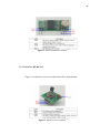
The components that had being transferred to the PCB as in Figure 3.23.
Figure 3.23: Components that had being transferred to PCB
44
3.4.12 Setting Up the PCB Workspace
To set the snap grid, complete the following steps.
1.
Select Design > Board Options.
2.
Set the values of Snap Grid and the Component Grid to 25mil.
3.
Click OK to close the dialog.
3.4.13 Component Positioning and Placement Options
Select Tools > Preferences. Open the PCB Editor – General page. In the
Editing Options section, make sure the Snap to Center option is enabled. This step is
done in order to enable the user to grad the center of the components.
3.4.14 Setting Up the Design Rules
The PCB Editor is a rules-driven environment, meaning that as you perform
actions that change the design, such as placing tracks, moving components, or
autorouting the board, Altium Designer monitors each action and checks to see if the
design still complies with the design rules.
If it does not, then the error is
immediately highlighted as a violation. Setting up the design rules before you start
working on the board allows you to remain focused on the task of designing,
45
confident in the knowledge that any design errors will immediately be flagged for
your attention.
1.
Select Design > Rules.
2.
Ten Categories will appear. Click once on each rule to select the rule that is
wished to modify. In this project mostly of the design rules are set to default.
3.
In our UTM PCB lab, the smallest Width of the connection is 25mil. Hence,
the Design Rule for Width had to be changed by select Width and set the
Width setting as the following values.
4.
Min Width = 25mil
Preferred Width = 25mil
Max Width = 25mil
Click OK to close.
3.4.15 Positioning the Components on the PCB
The components in Figure 3.24 need to be arranged neatly in order to reduce
the circuit‟s size.
1.
Left-click and hold the component in order to put it to the place we desired.
2.
The rotation of the components is the same as rotating components in the
schematic editor.
3.
If we desired to put the component to the other side of the PCB board, we
hold the left-click and press „L‟.
4.
The arranged components of my project are as shown in Figure 3.24.
46
Figure 3.24: Arranged components
3.4.16 Routing the Board
There are two methods in order to route the components. They are the
interactively routing the board and automatically route the board. In this project, I
had chosen the second method which is automatically routing the board.
1.
Un-route the board by selecting Tools > Un-Route > All.
2.
Select Auto Route > All. A report page will showed up.
3.
Click Route All.
4.
If we are not satisfy with the result, we can un-route and route as many times
as we like in the way by changing the position of the components.
47
3.4.17 Verifying the Board Design
The design rules that we had set at the starting of the design process can be
verify and it is a must to verify out design in order to avoid some circuitry problem
when we want to fabricate the PCB board.
1.
Select Design > Board Layer & Colours and ensure the Show checkbox
next to DRC Error Markers option in the System Colours section is enabled
so that the DRC error markers will be displayed.
2.
Select Tools > Design Rule Check.
3.
The Design Rule Verification Report will show the errors that does not
follow the design rules. Hence, errors must be fixed and repeat step 1 until
Warnings: 0 and Rule Violations: 0.
4.
Figure 3.25 shows the Design Rule Verification Report of my project that is
following the design rules.
Figure 3.25: Design rule verification report
48
CHAPTER 4
PROJECT IMPLEMENTATION
4.1
Introduction
In this chapter, the circuit drawn using schematic editor and the PCB layout
drawn by using Altium Designer Summer 09 will be shown. The connection and
interface between microcontrollers will be visualized and the complete programming
code will be attached in the Appedix.
4.2
The Control Unit (CU)
The control unit, CU consists of a microcontroller, PIC 16F877A, a
transmitter and three push buttons which represent the reset button, push button 1
and push button 2. When the push button is being pushed, the transmitter will
transmit the signal to communicate with the receiver.
diagram of the control unit.
Figure 4.1 is the block
49
Figure 4.1: Control unit block diagram
4.3
The Remote Unit (RU)
The remote unit, RU consists of a microcontroller, PIC 16F876A, a receiver,
a LED, and a buzzer. When the receiver received the signal that is being transmitted
from the transmitter, it will communicate with the microcontroller to buzz the buzzer
and turn on the LED. Figure 4.2 shows the block diagram of the remote unit.
Figure 4.2: Remote unit block diagram
50
4.4
Transmitting and Receiving Flowchart
Figure 4.3: Transmitting process flowchart
Figure 4.4: Receiving process flowchart
51
Flowchart shows the overall process of the project‟s operation. Figure 4.3
shows the flowchart for the transmitting process while Figure 4.4 shows the
flowchart for the receiving process. When the power supply of the control unit
turned on, the signal of 0xAA and 0xBB start to transmit. This is done in order to
increase the stability and the sensitivity of the receiving process. When there is no
switch being pressed, the signals send continuously. However, when the switch is
being pressed, the address that is being defined for each switch will be send to the
receiver. The receiver is receiving the 0xAA and 0xBB signal continuously and will
be interrupted when any of the switches is being pressed. For example, for the
remote unit 1, when switch 1 is being pressed, uart_sent will send a signal
0b00110011 to the receiver and received by the receiver. Hence, the receiver will
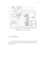
interface with the microcontroller and buzzed the buzzer and turned on the LED.
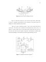
4.5
PIC Interfacing
The schematic of the PIC interfacing circuits is being drawn by using the
Altium Designer Summer 09. After that, the schematic will be transferred into the
PCB layout that will be done by the same software.
52
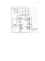
Figure 4.5: Transmitter schematic diagram
53
Figure 4.6: Receiver schematic diagram
4.6
PCB Board Interface
PCB board interface shows the PCB layout drawn using the Altium Designer
Summer 09 and the fabricated PCB board using the equipments that are available in
the UTM PCB Lab.
54
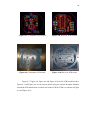
Figure 4.7: Transmitter PCB Layout
Figure 4.8: Receiver PCB Layout
Figure 4.9: Transmitter PCB board
Figure 4.10: Receiver PCB board
Figure 4.7, Figure 4.8, Figure 4.9 and Figure 4.10 are the PCB board interface.
Figure 4.7 and Figure 4.8 are the layout drawn using the Altium Designer Summer
09 and the PCB boards that are fabricated in the PCB lab UTM is as shown in Figure
4.9 and Figure 4.10.
55
4.7
Programming Coding
Figure 4.11: Transmitter coding
Figure 4.12: Receiver coding
Figure 4.11 and Figure 4.12 show how the signal transmit and receive.
56
1. These lines show that the 0xAA and 0xBB will be send continuously from the
control unit via the transmitter to the remote unit.
2. There is an interrupt, which is represent by button = = 0. This means that,
when the first button is being pressed, the address 00110011 will be send
from the transmitter to be received by the receiver.
3. These lines of coding will instruct the transmitter to continuously send the
signal of 00110011 when the button is being hold down.
4. CREN will be equal to one means data will be sent continuously. Other than
that, OERR condition also will equal to zero means RCREG still do not full.
5. In order to increase the stability and sensitivity of the signal receiving process,
these lines are needed.
The receiver will receive the 0xAA and 0xBB
continuously as long as the power supply of the control unit is ON.
6. When the signal address for button 1 is being detected, the PIC will instruct
the buzzer to buzz.
7. The LED will also be turned ON.
57
CHAPTER 5
RESULT
This chapter shows the result of the surface mount components that are
completely mounted on the PCB board. Besides, the functionality of the remote
locator will be record in the form of table.
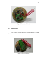
5.1
Control Unit (CU)
Figure 5.1 shows the control unit that was completely mounted on the PCB
board.
58
Figure 5.1: Transmitter PCB board
5.2
Remote Unit (RU)
Figure 5.2 shows the remote unit that was completely mounted on the PCB
board.
Figure 5.2: Receiver PCB Board
59
5.3
Remote Locator Capability
The remote locator with the transmitter and receiver modules is able to
operate in both with antenna and without antenna condition.
Obviously, with
antenna, the capability to locate the unit produces a better result. Table 5.1 will
conclude the capability of the remote locator.
Table 5.1: Remote locator capability
60
CHAPTER 6
CONCLUSION
This thesis had discussed about the development and fabrication on the
products with the title of “Surface Mount Technology Microcontroller Based Radio
Frequency Signal Remote Locator”. The objectives that are stated in Chapter 1 had
been successfully achieved.
I had developed the communication between
microcontrollers using RF signal, minimize the size of the circuits, able to locate the
missing items, and save the precious time of the user.
6.1
Introduction
As a conclusion, the project is success. The microcontrollers which consist
of PIC 16F877A and PIC 16F876A are able to communicate with each other by
using the radio frequency signal. Besides, the size of the circuits had being reduced
by more than half from the original circuits. The circuits can be manufactured into
the size of a key chain and it will be easier to bring along with. Last but not least, the
loud distinctive sound from the buzzer is very loud and clear, hence, it can save the
user precious time by locate the missing items without searching them.
61
6.2
Problems
During the development process, quite a numbers of problems occurred. First,
the surface mount PICs are not available in the shops. The only way to acquire the
PIC is ordered online. The time taken for the PIC arrived had shortened my time to
fabricate the PCB board.
Beside, the work in soldering the surface mount
components onto the PCB board is a skillful and tough work. Practice is the key to
make the soldering success. In addition, the surface mount PICs are sensitive to
unstable voltage. Unstable voltage will damage the surface mount PIC. Lastly, the
problem that unexpected is the machinery vibration problems. After I had done the
fabrication job, I had tested on the functionality of my products. The remote locator
worked. However, after I drilled the complete fabricate PCB board in order to get
the size of circle, the products cannot function anymore. In conclusion, handling
with surface mount PICs and components need technical and skills. Hence, we
should handle them with care.
6.3
Project Improvement
RFID RF module can be implemented in the future. Although the price of a
RFID is more expensive, however, the functionality of the remote locator will be
better. Besides, a transceiver can be used in order to increase the sensitivity of the
remote locator and increase the range of sensing.
62
REFERENCES
1. Myke Predko, “Programming and Customizing the PIC Microcontroller” 3 rd
Edition, Mc Graw Hill, United State, 2008.
2. Peter J. Boden, “Surface Mount Technology – A study of Safety
Considerations: Silver Migration and Adhersive Flammability”, February
1994.
3. Lawrence D. Rosenthal, “Paired Lost Item Finding System”, Oakland, CA
(US), September 2000.
4. Steve Yessa, “Microcontroller-Based Remote Locator Using Asynchronous
Serial Communication”, Bradley University Peoria, IL, March 2003.
5. Suhaila binti Mohd. Najib, “Microcontroller Based Remote Locator Using
Radio Frequency Signal”, UTM, Malaysia, 2010.
6. http://en.wikipedia.org/wiki/Surface-mount_technology
7. http://www.cellphonesafetyguide.com/questions/radiofrequency-energy
8. http://www.mikroe.com/forum/viewtopic.php?t=10057
9. http://www.piclist.com/techref/microchip/osc.htm
10. http://www.ip-extreme.com/IP/usart.shtml
11. http://en.wikipedia.org/wiki/Universal_asynchronous_receiver/transmitter
12. Mohannad Faaiz Bin Jamaluddin, “Wireless Heart Rate Monitor”, UTM,
Malaysia, 2008
13. http://ww1.microchip.com/downloads/en/DeviceDoc/usart.pdf
14. http://en.wikipedia.org/wiki/Universal_asynchronous_receiver/transmitter
15. ISM Band : http://en.wikipedia.org/wiki/ISM_Band
16. Cytron Technologies Sdn. Bhd. RF-TX-433 RF Transmitter Module User’s
Manual V1.1. Malaysia: Cytron Technologies Sdn. Bhd. 2008.
63
17. Cytron Technologies Sdn. Bhd. RF-RX-433 RF Receiver Module User’s
Manual V1.1. Malaysia: Cytron Technologies Sdn. Bhd. 2008.
18. http://cytron.com.my/viewProduct.php?pid=BCkGCi8vICQhMTcqPAcwD0!
!!!!uxmtQ4nUjOwKZrpHQCSw=
19. Cytron Technologies Sdn. Bhd. UIC00A_&UIC-S User Manual. Malaysia:
Cytron Technologies Sdn. Bhd. 2008.
20. Programmer : http://en.wikipedia.org/wiki/Programmer_(hardware)
21. Marlin Bates, “PIC Microcontroler An Introduction to Microelectronics”,
Elsevier Ltd., 2004.
22. Altium Designer Summer 09 User‟s Manual
64
APPENDIX A
Transmitter‟s coding.
//===========================================================
==============
// Coding for Transmitter
//===========================================================
==============
#include <htc.h>
//===========================================================
==============
//configuration
//===========================================================
==============
__CONFIG (0x3F3A);
//===========================================================
==============
// define
//===========================================================
==============
#define button RA0
#define button2 RA1
#define button3 RA2
65
//===========================================================
==============
// function prototype
//===========================================================
==============
void uart_send(unsigned char data);
void delay(unsigned long data);
void send_char(unsigned char data);
void send_config(unsigned char data);
//===========================================================
==============
// main function
//===========================================================
==============
void main(void)
66
{
//assign variable
unsigned char no,ptr,data;
ADCON1= 0x06; //configure PortA as digital I/O
TRISA = 0b111111; //configure PORTA input
TRISB = 0;
TRISD = 0;
InitLCD();
//setup USART
BRGH = 0; //baud rate for low speed option
SPBRG = 255; //set boud rate to 1200bps for 20Mhz
TX9 = 0; //8-bit transmission
TXEN = 1; //enable transmission
SYNC = 0; //asynchronous
SPEN = 1; //enable serial port
//===========================================================
==============
//Send enable signal
//===========================================================
==============
no=0xAA;
uart_send(no);
no=0xBB;
uart_send(no);
if(button==0)
{
{
no=0b00110011; //send the id number
}
while(button==0)
uart_send(no); //continuous send data
}
else if(button2==0)
67
{
{
no=0b11001100; //send the id number
while(button2==0)
uart_send(no); //continuous send data
}
else if(button3==0)
{
{
no=0b11110000; //send the id number
}
while(button3==0)
uart_send(no); //continuous send data
}
}
}
//===========================================================
==============
// functions
//===========================================================
==============
void uart_send(unsigned char data)
{
while(TXIF==0); //only send the new data after the previous is sent
TXREG=data;
}
68
APPENDIX B
Receiver‟s coding
// Coding for RECEIVER 1
//===========================================================
=============
#include <htc.h>
//===========================================================
==============
// configuration
//===========================================================
==============
__CONFIG (0x3F3A);
//===========================================================
==============
// define
//===========================================================
==============#define buzzer RC1
//===========================================================
==============
// function
//===========================================================
==============
69
unsigned char uart_rec(void);
//===========================================================
==============
// main function
//===========================================================
==============
void main(void)
{
//assign variable
unsigned char no;
//set I/O input output
TRISC= 0b10000000;
//setup USART
BRGH = 0; //baud rate for low speed option
SPBRG = 255; //set baud rate to 1200bps for 20Mhz
SPEN = 1; //enable serial port
RX9 = 0; //8-bit reception
CREN = 1; //enable reception
while(1) //infinity loop
70
{
CREN=1;
if(OERR==0)
{
if(uart_rec()==0xAA)
{
if(uart_rec()==0xBB)
{
if(uart_rec()==0b00110011)
buzzer=1;
else
buzzer=0;
}
}
}
else
CREN=0;
}
}
//===========================================================
==============
// functions
//===========================================================
==============
unsigned char uart_rec(void) //receive uart value
{
unsigned char rec_data;
while(RCIF==0); //wait for data
rec_data = RCREG;
return rec_data; //return the received data
}