1
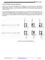
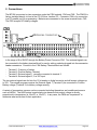
V104 Vehicle Power Supply
PC/104 DC to DC Converter
Technical Manual
P/N: V104-MAN
Revision: 30 Jun 2009
Revision
Date
A
6/26/2009
Comment
Initial version
FOR TECHNICAL SUPPORT
PLEASE CONTACT:
[email protected]
Copyright
© June 2009
Copyright
2009
Diamond Systems Corporation
1255 Terra Bella Ave.
Mountain View, CA 94043 USA
Tel 1-650-810-2500
Fax 1-650-810-2525
www.diamondsystems.com
CHAPTER 1 - INTRODUCTION.......................................................................................................................................................................................4
1.1 GENERAL DESCRIPTION.............................................................................................................................................................................4
1.2 FEATURES ....................................................................................................................................................................................................5
1.3 SPECIFICATIONS .........................................................................................................................................................................................6
CHAPTER 2 - CONFIGURATION AND INSTALLATION .................................................................................................................................................7
2.1 INTRODUCTION .................................................................................................................................................................................................7
2.2 Power Considerations ....................................................................................................................................................................................8
2.3.1 Main Input Power Connector.......................................................................................................................................................................8
2.3.2 AC Input Power Connector .........................................................................................................................................................................8
2.3.3 Output Power Connector.............................................................................................................................................................................9
2.3.4 Battery Power Connector (Optional) ...........................................................................................................................................................9
2.3.5 Onboard DC "Boost" Convertor (Optional)…………………………………………………………………………………………..9
2.4 Bus Termination (Optional) ………………………………………………….………………………………………………………….10
2.5 Installation onto PC/104 modules ……………………………………………………………………………….…………………...…10
2.6.1 LED Jumper Enable/Disable …………………………………………………………………………………….…………………....10
2.6.2 Mezzanine Expansion Headers ………………………………………………………………….…………………………………….11
2.6.3 PC/104 Bus Interupts (Optional) ………………………………………….……………………………………………………….....12
2.7 V104 Efficiency and Heat Dissipation Calculation ………………………………………………………………………………..…13
2.8 Power Management Controller PM104 (Optional) …………………………………………………………………………….…....14
CHAPTER 3 -THEORY OF OPERATION………………………………………………………………………………………………….…….15
3.1 Input power protection ……………………………………………………………………………………….……………………...…...15
3.2 Switching regulator, +5VDC …………………………………………………………………………………..………………..………15
3.3 Switching regulator, +12VDC ………………………………………………………………………………….……………….….…...15
3.4 Filter Capacitors ………………………………………………………………………………………………………………..…………16
3.5 Bus Termination (Optional) ……………………………………………………………………………………………………..……….17
A
A
A
A
P
P
P
P
P
P
P
P
E
E
E
E
N
N
N
N
D
D
D
D
I
I
I
I
X
X
X
X
1
2
3
4
…
…
…
…
…
…
…
…
…
…
…
…
…
…
…
…
V104 User Manual Rev A
…
…
…
…
…
…
…
…
…
…
…
…
…
…
…
…
…
…
…
…
…
…
…
…
…
…
…
…
…
…
…
…
…
…
…
…
…
…
…
…
…
…
…
…
…
…
…
…
…
…
…
…
…
…
…
…
…
…
…
…
…
…
…
…
…
…
…
…
…
…
…
…
www.diamondsystems.com
…
…
…
…
…
…
…
…
…
…
…
…
…
…
…
…
…
…
…
…
…
…
…
…
…
…
…
…
…
…
…
…
…
…
…
…
……………..
……………..
..……………
..……………
.…
.…
….
….
Page 2
1
1
1
2
8
9
9
1
PREFACE
This manual is for integrators of applications of embedded systems. It contains information on hardware requirements
and interconnection to other embedded electronics.
DISCLAIMER
Diamond Systems makes no representations or warranties with respect to the contents of this manual, and specifically
disclaims any implied warranties of merchantability or fitness for any particular purpose. D iamond Systems shall under no
circumstances be liable for incidental or consequential damages or related expenses resulting from the use of this product,
even if it has been notified of the possibility of such damages. D iamond Systems reserves the right to revise this publication
from time to time without obligation to notify any person of such revisions. If errors are found, please contact D iamond
Systems at the address listed on the title page of this document.
COPYRIGHT © 2009 Diamond Systems
No part of this document may be reproduced, transmitted, transcribed, stored in a retrieval system, or translated into any
language or computer language, in any form or by any means, electronic, mechanical, magnetic, optical, chemical,
manual, or otherwise, without the express written permission of D iamond Systems .
V104 User Manual Rev A
www.diamondsystems.com
Page 3
CHAPTER 1 - INTRODUCTION
1.1 GENERAL DESCRIPTION
The V104 multiple output DC to DC 25 watt converter is a versatile, “bullet-proof” unit that can be
supplied with as a +5V, outputs only or can include features such as Power Management, Universal
Battery Charger, AC Bus termination, +12V output, -5V output, -12V output and custom output
voltages from –42V to +42V. The V104, designed for embedded PC/104 computer systems, has a
wide input range of 8 to 30V (>6:1) and is ideal for battery or unregulated input applications or low
voltage AC inputs. The V104 is specifically designed for vehicular applications. It has heavy-duty
transient suppressors (5000W) that clamp the input voltage to safe levels, while maintaining normal
power operation. Battery, DC and AC input configurations from 8 to 30V are all handled by the V104
automatically.
The V104 is a “simple switcher” based design that provides outstanding line and load regulation with
efficiencies up to 80 percent. Organic Semi conductor capacitors provide filtering that reduces ripple
noises below 30mV. The low noise design makes the V104 ideal for applications wherever EMI or
RFI must be minimized. The +5VDC and +12VDC outputs are controlled by a constant off-time
current-mode architecture regulator, which provides excellent line and load transient response.
The +12VDC boost regulator uses the +5VDC as input power and therefore can operate without
dropout from 8 to 30V input and supply 1A.
A “plug-in” Universal Battery Charger (UBC104) is available for the V104 to charge Lead-Acid, NiCd
and NiMh batteries. Charge currents can be up to 1.5A and battery charging voltages from 8 to 30V.
The Power Management controller (PM104) allows timed on/off control of the V104, bus interrupts on
impending power failure, current limit setting and intelligent charge termination for the UBC104.
The V104 is provided in a PC/104 form factor compliant size, which includes the 8bit and 16bit
PC/104 expansion bus header. All generated voltages are provided to their related power supply pins
on the PC/104 expansion bus and are all also available for off-board use through a screw terminal
block. PC/104 AC bus termination is optionally available on the V104, which provides the cleanest
possible signals on the PC/104 bus.
The V104 can be configured to meet almost any power supply need for embedded PC/104
applications, whether that be a simple +5V application, providing power for back lighted LCD panels
or a full UPS (uninterruptible power supply configuration).
V104 User Manual Rev A
www.diamondsystems.com
Page 4
1.2 FEATURES
-
DC to DC converter for PC/104 bus equipped products.
“Load Dump” transient suppression on input power supply.
Operates from 8VDC to 30VDC input.
“Stacks” onto the PC/104 bus.
Passthrough or non-passthrough 8 bit and 16 bit versions.
+5V standard, +12V, -12V, -5V and battery charger optional.
Highly compact, 100 percent PC/104 conforming.
AC bus termination available.
Screw terminals blocks for off-board connection to outputs.
V104 User Manual Rev A
www.diamondsystems.com
Page 5
1.3 SPECIFICATIONS
Power Supply Specifications
Model
V104
5V output*
5A
12V output
1A
-5V output
400mA
-12V output
160mA
Input Voltage Range
8 to 30V
Load Regulation **
<30mV
Line Regulation **
+ 40mV
Output temp. drift **
<10mV
Switching Freq.
100kHz
Output Ripple**
<40mV
Conducted Susceptibility**
>57db
Efficiency**
Up to 80%
Temp Range
0 to 70C
Quiescent current***
22mA
Weight
150 grams
Size, PC/104 form factor compliant****
3.55"W. x 3.75"L x 0.6" Height
*Current rating includes current supplied to 12V, -12V, & -5V regulators.
** Measured on the 5V output.
***LEDs disabled.
****Not including passthrough pins.
V104 User Manual Rev A
www.diamondsystems.com
Page 6
CHAPTER 2 – CONFIGURATION AND INSTALLATION
2.1
Introduction
This chapter describes the configuration and installation of the V104 power supply. In addition,
section 2.2 provides a formula to calculate the available +5VDC. Figure 2-1 shows the V104
connectors, jumper and other options.
Figure 2-1, V104 Connector and Jumpers
V104 User Manual Rev A
www.diamondsystems.com
Page 7
2.2
Power Considerations
The +5V switching regulator is rated at 5A maximum output however, the +5V output supplies power
to the +12, -5 and –12VDC regulators. The usable range of the +5V output can be calculated using
the following derating formula.
Usable +5VDC output = 5A-(I[-5] +I[12]*2.4) /0.80)
Where:
I[-5] = -5VDC current load
I[-12] = -12VDC current load
I[12] = 12VDC current load
Assuming 80 percent converter efficiency (actual efficiency may vary).
2.3.1 Main Input Power Connector
Input power is connected to the “pluggable” block, CN1, which is removable from the socket
connector on the circuit board. The power supply accepts DC input voltages in the range of 8VDC to
30VDC.
Unregulated vehicle power is connected as follows:
-
Terminal 1: “hot” polarity
Terminal 2: Common (0VDC)
!! CAUTION !!
To allow operation at the lowest possible input voltages (8VDC) and for the best efficiency, there is
NO input reverse-polarity diode provided on the V104 main DC input connector. If reversepolarity protection is required, connect to the AC input connector. See section 2.3.2
2.3.2 AC Input Power Connector (Optional)
Low voltage AC is connected to the V104 on screw terminal block, CN7. The V104 accepts AC
power in the range of 6VAC to 20VAC however, 12VAC to 16VAC is the recommended range. The
input capacitor on the V104 is 1000uF and is adequate for low power applications drawing one amp.
Connect an additional 1000uF capacitor to connector CN1 (terminal 1, positive, terminal 2 negative)
for greater loads.
V104 User Manual Rev A
www.diamondsystems.com
Page 8
2.3.3 Output Power Connector
Output power is available for non-PC/104 use via connector CN2.
-
Terminal 1: +5VDC output
Terminal 2: Common
Terminal 3: +12VDC output (optional)
Terminal 4: -12VDC output (optional)
Terminal 5: -5VDC output (optional)
2.3.4 Battery Power Connector (Optional)
The batteries are connected to the screw terminal block, CN3. The V104 accepts DC battery
voltages in the range of 8V to 30VDC through the Battery Power Connector. Two external signals
can be connected to the battery terminal block for use by add-on modules plugged into the
mezzanine header connectors. Connect to the V104 Battery Terminal Block as follows:
-
Terminal 1: Common of battery
Terminal 2: Positive Battery Terminal
Terminal 3: External signal 1
Terminal 4: External signal 2
Note:When optional Plug-IN Boost regulator (VR3) is ordered, batteries or external signals cannot
be connected to CN3. See section 2.3.5
2.3.5 Onboard DC “Boost” Converter (Optional)
Three optional converter “boost” pumps (model NMH05XXS, XX = output voltage, +5V, +9V, +12V,
+15V) can be installed on the V104. The NMH charge pumps have a maximum 2 watt capacity, but
require a minimum load of 10 percent for proper operation.
The –5V output is generated by installing a NMH0505S in location VR4 and adding capacitor C7.
The –5V output is available on the PC/104 bus (B-7) and on connector block CN2, terminal 4.
The third optional converter is used for generating custom voltages, which is installed in location VR3
and adding capacitors C4 and C8. The NMH charge pumps have an isolated positive and negative
output. By referencing (connecting) the charge pump to other voltages, the user can create +/supplies, elevated and negative voltages (ie. The charge pump “0V” is not connected to the V104
common).
-
Terminal 1: Common of battery
Terminal 2: -V output
Terminal 3: 0V
Terminal 4: +V output
V104 User Manual Rev A
www.diamondsystems.com
Page 9
Example: NMH0515S (+15V) can generate the following voltages:
- +15V by connecting NMH “0V” to V104 common
- -30V by connecting NMH +V to common
- +30V by connecting NMH –V to common
- +42V by connecting NMH –V to +12V output
Note: When batteries or external signals are connected to CN3 the Plug-IN Boost regulator (VR3)
cannot be installed. See section 2.3.4
2.4
Bus Termination (Optional)
AC bus termination minimizes power consumption, while improving the reliability of the bus. The
resistor/ capacitor combination only conducts current during the few nanoseconds when the bus signal
is changing state.
2.5
Installation onto PC/104
The PC/104 bus on the V104 is keyed according to the standards as set out be the PC/104 Consortium
Guidelines. Male Pin B10 of the 8-bit bus and male pin C20 of the 16-bit bus are removed but the female
sockets are not “plugged”.
Because of the large number of pins and sockets (104 total) in the PC/104 bus, caution must be used
in separating the PC/104 modules to prevent bending the pins or hurting the person separating the
modules. Diamond Systems recommends the use of the PC/104 removal tool (model #5535), available
from Diamond Systems.
2.6.1 LED Jumper Enable/Disable
These jumpers allow the LEDs to be disabled. This is most likely to be used when absolute minimum
power consumption must be maintained, such as when operating off a limited battery source.
The location of each LED jumper is immediately behind each LED.
Each LED is enabled by factory default. To disable any LED, remove the LED jumper (or cut the
small PCB trace if no jumper is installed) associated with the LED. To re-enable any LED, re-install the
associated jumper (or solder a short jumper wire between each of the jumper pads).
V104 User Manual Rev A
www.diamondsystems.com
Page 10
2.6.2 Mezzanine Expansion Headers
The mezzanine expansion headers are used for installation of the optional battery charger. The
mezzanine expansion headers can also be used for custom output voltages such as Vee for LCD panels.
If custom output voltages are required please contact Diamond Systems.
Figure 2.3, V104 Mezzanine Connectors
Connector CN5 Pinout
1. +5V
10. +5V
Connector CN6 Pinout
1. PM104-P1
10. Main Pwr. Input
2. Common
9.Common
2. Common
9. Common
3. +Battery Input
8. Main Pwr Input
3. PM104-P7
8. PM104-P2
4. Ext. Signal 1
7. +12V
4. PM104-P6
7. PM104-P3
5. Ext. Signal 2
6. -5V
5. PM104-P5
8. PM104-P4
V104 User Manual Rev A
www.diamondsystems.com
Page 11
2.6.3 PC/104 Bus Interrupts (Optional)
Interrupts to the PC/104 bus require the installation of the optional power management
mircrocontroller (PM104). The PM104 can be programmed to provide indication of loss of input
power, low battery voltage or to provide indication to the PC/104 CPU to begin an orderly shutdown of
program operation.
Two separate interrupt requests can be generated and each interrupt request will remain active until
the cause of the interrupt request returns to normal. Interrupt Int1 can be set to IRQ6 or IrQ7, while
Int2 can be set to IRQ4 or IRQ5 by installing a appropriate jumper on jumper selectons block J4.
Jumper block J4 is located adjacent to the PC/104 bus, on the opposite end where the power LEDs
are located.
Figure 2-2, Interrupt IRQ Selection
V104 User Manual Rev A
www.diamondsystems.com
Page 12
2.7
V104 Efficiency and Heat Dissipation Calculation
The typical efficiency of the V104 is 80 percent for the +5V output, but efficiency at any specific input
voltage, output load and ambient temperature may be higher or lower. Typical efficiency is between
70 and 85 percent. Best efficiency occurs at mid input voltage (16 to 18V), mid output loads (10 to 18
watts) and low heat sink temperature. As the input voltage and output load is determined by the
system application, this leaves only the heat sink temperature that System Integrators adjust to
maximize efficiency. Either forced flow fans or thermally coupling the V104 heat sink to enclosures or
external heat sinks can improve the efficiency of the V104. Good thermal management can obtain an
improvement of 3 to 4 percent. The results are that 35 percent less heat is dissipated.
A) Heat Dissipated (HD) = Input Power – Actual Load
Where Input Power = Input Voltage * Input Current
And Actual Load = +5V +(+12V load) + (-5V load) + (-12V load)
(load measured in watts).
B) Estimated Heat Dissipated (ESD) can be calculated based on 80 percent efficiency:
EHD = {+ 5V load + [(+12V load) + (-5V load) + (-12V load)]/0.8} * 0.2
C) If the Battery Input option is installed additional heat will be dissipated.
BID = Total Load/ Battery Voltage *0.7V (diode drop)
D) If the AC Input option (full bridge) is used additional heat will be dissipated.
ACID = Total Load/ Voltage *1.4 V (2 diode drop)
E) If the Battery Charger Option is installed the heat dissipated from it will vary according to the
current charge current and can be estimated by:
BCD = Maximum Charge Current * charge Voltage * 0/1
(based on 90 percent efficiency).
V104 User Manual Rev A
www.diamondsystems.com
Page 13
2.8
Power Management Controller PM104 (optional)
The Power Management Controller (PM104) is a microcontroller “plug-in” module for timed on-off
control of the V104, control of the optional battery charger and generation of interrupts to the PC/104
host CPU. The PM104 is programmed in a high level “controller basic language” called Pbasic. To
program the PM104, connect the program cable (PM104-Cable) to connector CN4 on the V104 and
to the parallel port of any PC compatible computer. PM104 programs can be directly downloaded or
updated using the PM104 utility software.
-
Connector CN4 Pinout, PM104 Program Connector
Terminal 1: PM104 Power (leave disconnected if V104 powered)
Terminal 2: Common, connect to pin 25 of PC parallel port
Terminal 3: PC0, connect to pin 11 (busy) of PC parallel port.
Terminal 4: PCI, connect to pin 2 (DO) of PC parallel port.
Table 2.1 PM104 Pin Number and I/O Functions
IC3 PIN
PM104 Microcontroller
Description (IC3)
V104 Function or Connection
Battery Charger Function
1
PM104 Supply Voltage
V104 Supply Voltage
2
Common
Common
3
PC0 (PC out)
Connector CN4-3
4
PCI (Pc in)
Connector CN4-4
5
Plus 5V input/output
No connection
6
Reset
No connection
7
P0 (Input/Output Pin 0)
Input Voltage Status
8
P1 (Input/Output Pin 1)
V104 On/Off Control
V104 On/Off control
9
P2 (Input/Output Pin 2)
Connector CN6-8
Analog/Digital Chip Select
10
P3 (Input/Output Pin 3)*
Int2, Connector CN6-7*
Spare* Input/Output
11
P4 (Input/Output Pin 4)
Connector CN6-6
Data Input/Output Line
12
P5 (Input/Output Pin 5)
Connector CN605
Data Clock
13
P6 (Input/Output Pin 6)*
Int1, Connector CN6-4*
Spare* Input/Output
14
P7 (Input/Output Pin 7)
Connector CN6-3
Analog Current Limit
•
If interrupt function is not used, this PM104 line can be used for general purpose Input/Output.
V104 User Manual Rev A
www.diamondsystems.com
Page 14
CHAPTER 3 – THEORY OF OPERATION
3.1 Input power protection:
Input power is connected to the screw terminal block, CN1, which is removable from the socket
connector on the circuit board. A seven ampere ‘pico’ fuse F1 limits the current draw from the power
source. A series of devices, (toroid coil L3, transorb D4 and filter capacitor C12) filters and clamps
the input power.
Transorb D4 is a 5KVA, heavy duty transient suppressor that provides “zener” type protection and
has an avalanche voltage of 33V. It is electrically located before fuse F1 to prevent activation of the
fuse during a “load dump” or large transient. Sustained voltages greater than the avalanche voltage
must not be applied or transorb D4 will fail.
3.2 Switching regulator, +5VDC
A simple switcher regulator VR1, generates the +5VDC output, operating in a “buck” mode switching
regulator configuration using inductor coil L1, schottky diode Z1, input filter capacitors C12 and output
filters capacitor C6. Regulator VR1 is a current mode controller and adjusts the “switching cycle” by
the sensed current rather than directly by the output voltage. Control of the output voltage is obtained
by using the output of a voltage sensing error amplifier in regulator VR1 to set the current trip level.
A total of 5 amperes can be supplied to the connected +5VDC load, to the inputs of the +12VDC
regulator and the –5VDC and –12VDC charge pumps and invertors. The +5VDC power is available
on the PC/104 expansion bus (B3, B29 and D16) and screw terminal connector CN2. LED2 provides
indication of +5V operation.
3.3 Switching regulator, +12VDC
Switching regulator VR2 generates the +12VDC output, operating in a “boost” mode switching
regulator configuration using inductor coil L2, Schottky diode D11, input filter capacitor C6 and output
filters capacitor C3. Capacitor C6 works as an output filter for the +5VDC and as an input filter for the
+12VDC regulator VR2. Regulator VR2 is a current mode controller and adjusts the “switching cycle”
by the sensed current rather than directly by the output voltage. Control of the output voltage, sensed
by resistors R5 and R6, is obtained by using the output of a voltage sensing error amplifier in
regulator VR2 to set the current trip level. If a custom output voltage is ordered, variable resistor R21
(in series with R5) will adjust the feedback voltage.
A total of one ampere can be supplied to the connected +12VDC load and the –12VDC inverter. The
+12VDC power is available on the PC/104 expansion bus (B9) and screw terminal connector CN2.
LED1 provides indication of +12VDC operation.
V104 User Manual Rev A
www.diamondsystems.com
Page 15
3.4 Filter Capacitors
At 10kHz and above, the impedance of filter capacitors is essentially their effective series resistance
(ESR) and this parasitic resistance limits the filtering effectiveness of the capacitors. Since the filter
capacitors must absorb the “switching ripple” current, capacitors with high ESR values will quickly
overheat. For example, a capacitor with a 100mOhm ESR which is absorbing a 5A ripple current, will
dissipate 2.5W heat.
The capacitors used for filtering the +5V and +12V outputs in the V104 are organic semiconductor
(OS-CON) capacitors. The OS-CON is an aluminium solid capacitor with organic semi-conductive
electrolyte used as a cathode conductive materials. The OS-CON has many advantages over the
conventional electrolytic:
-
Very low ESR values, less than 8 times lower for same package.
High ripple current rating, over 4 times higher for same package.
No degrade in operation at extended low temperatures. (ESR value of conventional
electrolytics can increase 25 fold at –40C).
The life expectation for a filter capacitor is typically 2,000 to 6,000 hours @ 105C. For a conventional
electrolytic capacitor the temperature acceleration coefficient = 2 for a 10C increase, while the OSCON has a temperature acceleration coefficient =10 for a 20C increase. For example, a capacitor
rated for 2,000 hours @ 105C would have an expected life of:
-
-
for conventional electrolytic capacitor
32,000 hours (3.6 years) @ 65C
128,000 hours (14.6 years) @ 45C
for OS-CON capacitor
200,000 hours (22 years) @ 65C
2,000,000 hours (220 years) @ 45C
This means that the OS-CON has extremely longer life in practical use even under the same warranty
of 2,000 hours @ 105C.
In a buck convertor, output ripple voltage is determined by both the inductor value and the output filter
capacitor (for continuous mode).
Vp-p = ESR*Vout (Vout/Vin))
L1 * frequency
EXAMPLE
Vout = 5V, Vin = 16V, L1 = 55uH, frequency = 100kHz and 330uF capacitor with 27mohm
ESR.
Vp-p = 0.027 * 5 (1- (2/16))
55 * 10E-6 * 10E5
V104 User Manual Rev A
~17mV ripple
www.diamondsystems.com
Page 16
Note: only the ESR of the output capacitor is used in the formula. It is assumed that the
capacitor is purely resistive at frequencies above 20kHz. Worst case output ripple is at highest
input voltage and is independent of load.
3.5 Bus Termination (Optional)
AC bus termination is provided by 5 “RC” SOIC packages (3 only for 8-bit PC/104 bus), RC1 to RC5
and discrete components C20 and C27. Each RC package contains 16 resistor/capacitor
combinations of 47R and 47PF with a common bus connected to the signal ground.
1
2
3
4
5
6
7
8
9
10
11
12
13
14
15
16
17
18
19
20
RC1
GND
*SMEMW
AEN
IOCHRDY
SD0
SD1
SRDY
SD2
SD3
GND
GND
SD7
SD6
SD5
SD4
DRQ2
SA19
*SMEMR
SA18
GND
RC2
GND
IRQ10
LA22
IRQ11
LA21
LA20
IRQ15
LA19
LA18
GND
GND
*MEMR
LA17
LA18
IRQ12
LA23
*IOCS16
*SBHE
*MEMCS16
GND
RC3
GND
*BACK6
SD9
DRQ6
*DACK7
SD11
DRQ7
SD12
---GND
GND
SD15
SD14
SD13
SD10
SD8
DRQ5
*MEMW
*DACK5
GND
RC4
GND
SA11
*Refresh
SA12
DRQ1
SA13
*DACK1
SA14
SA15
GND
GND
*IOW
SA17
*IOR
SA16
*DACK3
DRQ3
IRQ7
SA10
GND
RC5
GND
SA3
BALE
SA4
IRQ3
SA5
*DACK2
SA6
SA7
GND
GND
IRQ6
SA9
IRQ5
SA8
IRQ4
DA2
SA1
SA0
GND
In addition, the following signals are terminated with discrete components.
- TC C1 (330pF)
- Reset C20 (330pF)
V104 User Manual Rev A
www.diamondsystems.com
Page 17
APPENDIX 1
Advantages of Using AC Termination
One of the requirements of embedded electronics is for low power consumption. One method
of reducing power is to reduce the drive current available to power the expansion bus. With
over 80 signal lines, any reduction in current load would have a large impact on overall
requirements. The PC/104 Consortium Guidelines for the expansion bus specify drive current
can be as low as 4mA. Compared with the 24mA for the standard desktop computer, this is an
84 percent reduction in the drive current available.
The disadvantage to reducing drive current is the increasing possibility for noise to infilitrate
the bus. The symptoms of noise induced problems are often “flaky” or unreliable operation.
Systems suffering from noisy busses are often difficult to diagnose and solve. Programmers
blame the hardware engineers and the hardware engineers blame the software programmers.
With reduced drive currents, more attention must be paid to reducing the noise levels on the
PC/104 bus. One frequently used method is bus terminators. Testing has proven the best
way to terminate the PC/104 bus is to use AC terminators instead of resistive terminators.
This is the recommended termination method for Ampro CPU products. The IEEE P996 PC
Bus Standard recommends the AC bus terminating technique.
The use of AC terminators has several advantages over DC terminators:
-
Reduced power consumption: DC terminators are typically in the 330 ohm to 1K ohm range
and draw heavy currents. This is significant when terminating the over 80 signals on the
PC/104 bus. AC terminators draw current only during the few nanoseconds when the bus
signal is changing state, resulting in negligible current drain.
-
Improved bus reliability: DC terminators invariably increase the voltage level of the logic
zero state. This decreases noise immunity, making it more likely a zero will be seen as a one.
AC terminators do not cause this shift, resulting in a more reliable bus.
-
Reduced crosstalk: AC terminators roll off the signal transitions on the bus. The result is a
quieter bus which has fewer high frequency effects such as crosstalk to other bus lines.
-
Reduced EMI. Busses with AC termination tend to generate less EMI than resistively
terminated buses due to the reduction in high frequency components of signal transitions.
V104 User Manual Rev A
www.diamondsystems.com
Page 18
APPENDIX 2
Installation Hints for the V104 Power Supply
1. To minimize noise induced into the power supply, connect the V104 power supply direct to the
power supply source (battery) with “dedicated” wires. This makes use of the vehicle battery as
a filter.
2. Always use large gauge hook-up wires to connect the V104 power supply to the vehicle power
source (battery). This minimizes any voltage drop caused by the resistance of the wire. Use
minimum of AWG #16 for lengths less than 10 feet and AWG #14 for longer lengths.
3. Wherever possible, install the V104 power supply on to the top of the V104 card stack. This
will allow better dissipation of heat from the heat sink. If additional cooling is required, use
either forced air ventilation or mount the PC/104 power supply so that the heat sink can
dissipate heat to the enclosure.
APPENDIX 3
Vehicles Are An Electronics Nightmare
Under the hood of a vehicle is an electronics nightmare. EMI spraying and RFI sparking is
everywhere and electrical transients run amuck, zapping the embedded electronics. Electronics
located in that environment must withstand 600V transients and “load dump” situations. Although
the automotive market is growing about 2 percent yearly, the amount of electronics being
introduced into vehicles is much higher. The electronics on a vehicle are no longer just the radio
and engine computer, but cellular phones, portable computers, faxes, smart navigation with
Global Positioning Receiver and car alarm systems.
The infamous “load dump” is an energy surge resulting from disconnecting the battery while being
charged. The alternator, with a finite response time of 40msec to 400msec, generates power with
nowhere to go. Thus an energy surge is formed; much like a tidal wave that builds to an
enormous height as it crashes the beach. The resultant over voltage is the most formidable
transient encountered in the automotive environment and is an exponentially decaying positive
voltage. The actual amplitude depends on alternator speed, the level of alternator field excitation
and can exceed 100V.
Each electronic component had its own power supply and it is the power supplies that must
absorb the transients and energy surges. What makes one transient more dangerous than
another transient is not the voltage level, but the amount of energy it carries. A600V, 1msec
transient had much less energy than a 100V, 400msec surge. Regardless of the source, all over
voltages must be clamped and prevented from passing through to the rest of the electronics.
There are a number of methods for clamping over voltages, but the most efficient and cost
effective is to shunt the current to ground using a surge suppressor. The surge suppressor relies
on the vehicle’s wiring and alternator impedance as the current limit and it remains in a high
impedance state until an over voltage condition occurs. Standard devices such as transorbs
(P6KE or 1.5KE) will not survive the high-energy discharge of a “load dump”. Special automotive
suppressors must be used to use up the 20A to 30A peak currents being shunted. Several
manufacturers, such as Motorola, Harris and Seimens, manufacture suppressors specifically for
V104 User Manual Rev A
www.diamondsystems.com
Page 19
automotive applications. Some devices provide “zener diode” style protection, while others
provide “back to back zener diode” bidirectional protection. Each type has advantages, but unless
they are used correctly, they will fail to protect the electronics. Ratings on the transient
suppressors can be confusing. A suppressor with an avalanche voltage of 24V to 32V will have a
clamp off voltage of over 40V. In addition, ambient temperature can vary from –40C to 70C and
can result in the avalanche voltage being several volts lower at –40C and a clampoff several volts
higher at 70C.
Not all vehicles have 12V battery systems. Some trucks use 24V batteries, aircraft use 28V and
trains from 45V to 85V. Transient suppressors for aircraft cannot use the 12V system automotive
components. Instead, a suppressor with an avalanche rating of 35V is needed to allow for low
ambient temperature compensation, but this results in clamp off of over 70V. Diamond Systems’
V104 Vehicle Power Supply, employs a Diode Inc. (part#5KP33A), allowing an input voltage range
of 8V to 30V. If a high clamp off voltage cannot be tolerated, other techniques must be used. A
series device such as a MOSFET can act as a pre-regulator, but it also must be selected to
withstand transients. In addition a series device adds to in-efficiency and creates a heat
dissipation problem, especially at high ambient temperatures.
“Load dumps” occur infrequently in a vehicle’s lifetime, but any electronics wishing to survive in
this environment must be designed to withstand the assaults. “Load dumps” co-operate slightly
through, their worst-case voltage does not typically occur with worst-case source impedance. In
fact, although the total energy of a “load dump” may be 500 joules, a transient suppressor capable
of 70 joules typically will be adequate because of the distributed electronics in the vehicles. That
is, provided the suppressor ratings are the same or larger than other suppressors throughout the
vehicle. A quick thinking engineer can take advantage of this and design his power supply to
withstand higher voltages and thus let others’ transient suppressors do the work.
V104 User Manual Rev A
www.diamondsystems.com
Page 20
APPENDIX 4
BC104 Battery Charger and PM104 Power Management Units
1) Description
When the BC104 and PM104 units are both installed on either the V104 (hereafter referred to as
PSU), a universal battery charger can be setup and the PSU unit made into an UPS
(uninterruptible power supply).
The BC104 is a constant current “buck” switching regulator with an adjustable “float” voltage. The
float voltage is adjusted via a potentiometer. The PM104 is programmed by the user using a
“control basic” called Pbasic. A sample program is supplied to show a typical NiCd charging
control. Before using the BC104 and the PM104 the battery charging program must be set up for
the intended battery pack. The sample program has separate settings for normal charge current
and trickle charge current. In addition, the charge termination methods should be set, including
maximum charge time, negative delta V. The user must set these for the type and size of battery
to be charged. Typically charge currents will be 1/3 to 1/6 of battery capacity and trickle charge
current 1/20 to 1/30 of battery capacity. Addition of a battery temperature sensor will allow charge
termination with elevated battery temperatures (which indicates battery is fully charged).
The PM104 can be programmed for many additional features not included in the sample program.
Features such as setting a PC/104 bus interrupt when main power fails, stopping the PSU after
running on battery backup power for a set time, tracking power consumption so that backup
battery charging can be terminated when the same amount is restored to the battery. These
features are left to the OEM integrate into their design.
V104 User Manual Rev A
www.diamondsystems.com
Page 21
2. Connections:
The BC104 is mounted on two connectors under the PSU heatsink, CN5 and CN6. The PM104 is
factory installed directly in front of the PC/104 bus, location IC3. Connector CN4 is for connection
to a PC parallel port for programming. Batteries are connected to the screw terminal block, CN3.
The PSU accepts DC battery voltages
in the range of 8 to 20VDC through the Battery Power Connector CN3. Two external signals can
be connected to the battery terminal block for use by add-on modules plugged into the mezzanine
header connectors. Connect to the V104 Battery Terminal Block as follows:
-
Terminal 1: Common of battery
Terminal 2: Positive Battery Terminal
Terminal 3: External signal 1, normally connected to terminal 2
Terminal 4: External signal 2, 0 to 30V input
The two external signals are fed into the 12 bit analog to digital converter and will accept voltages up
to 30V. The sample program requires the External signal 1 (Terminal 3) be connected to Positive
Battery voltage (Terminal 2) for battery voltage sensing.
A variety of temperature sensors can be connected including thermistors and conditioned sensors
such as LM35s. The LM35 series is particularly nice because their output voltage is directly
proportional to temperature (ie 10mV/C or 10mV/F). In any case, the OEM can “experiment” to
determine what works best in their application.
V104 User Manual Rev A
www.diamondsystems.com
Page 22
3. Programming Cable:
The programming cable is plugged into the connector CN4 on the PSU and the other end into the
25pin DB parallel port connector on a PC. The programming cable has the following connections:
CN4-1
CN4-2
CN4-3
CN4-4
No connection
Connect to pin 25 on parallel port
Connect to pin 11 parallel port
Connect to pin 2 parallel port
4. Download and Edit Software:
All programs for the PM104 are written in a “Control Basic” program language and are saved into
an ASCII file with a “BAS” extension. Any text editor can be used to create, edit and save these
programs. The Download program called “Stamp.exe” also has simple editing capabilities.
After the program cable is connected between the PSU and the parallel port, the PSU unit can be
turned on, thus providing power to the PM104 unit. The Download program Stamp. Exe is started
by typing from DOS, STAMP.EXE. The program to be downloaded is opened by pressing the
keys “ALT” and “L” simultaneously. Using the arrow keys select the desired file and press ENTER
key. To download the program press the keys “ALT” and “R” simultaneously. If the cable is
properly connected and power applied the screen will show a horizontal bar graph indicating the
percent of program downloaded. The red area of the bar graph is the portion used and the
remainder is program space available.
5. Program Command and Syntax:
Please refer to the Adobe files BSBOOK1.PDF and BSBOOK2.PDF.
6. Adjusting the BC104 Float Limits:
When a PC/104 power supply is equipped with a BC104 and a PM104 the BC104 has a Float
Voltage Adjust potentiometer. However, the Current Limit Adjust potentiometer is not installed
and is controlled via the PM104.
Using a small screwdriver (flexible nylon works best), turn the potentiometer until the desired float
voltage is obtained. No load should be present when adjusting.
V104 User Manual Rev A
www.diamondsystems.com
Page 23
7. Sample Battery Charging Program Listing
The following program listing is intended for use as a guide to customizing the BC104 and PM104
operation. Additional functions and features can be added including temperature monitoring are
left up to the OEM to implement.
BC104, Battery Charger Sample program code
SYMBOL
SYMBOL
SYMBOL
SYMBOL
SYMBOL
SYMBOL
SYMBOL
SYMBOL
SYMBOL
SYMBOL
SYMBOL
SYMBOL
SYMBOL
SYMBOL
SYMBOL
SYMBOL
Pwr_Status = 0
Pwrp_Status =pin0
PSU_On/Off = 1
PSUp_OnOff = pin1
CS1 = 2
CS1p = pin2
Int2 = 3
Int2p = pin3
DIO = 4
DIOp = pin4
CLK = 5
CLKp = pin5
Int1 = 6
Intp = pin6
Chrg_Limit = 7
Chrgp_Limit = pin7
‘ Status of input power
‘ Pin number of status of input power
‘OnOff control of power supply
‘ Chip select A/D on Battery Charger; 0=active
‘ PC/104 bus interrupt
‘ Pin_number_of data input/output.
‘ Variable_name_of date input/output.
‘ Clock to ADC; out on rising, in on falling edge.
‘ PC/104 bus interrupt
‘ PWM output for current limit
SYMBOL Bat_Set = bit1
SYMBOL Adbits = b1
SYMBOL Bat1_Chrg = bit1
SYMBOL D0 = bit2
SYMBOL D1 = bit3
‘ Counter variable for serial bit reception.
‘ LSB of ADC channel selection
‘ second bit of ADC channel selection
‘D1 = 0, D0 = 0 channel 0 input, pin3 of connector CN3
‘D1 = 0, D0 = 1 channel 1 input, pin4 of connector CN3
‘1. on max cell voltage
‘2. on time
‘3. –ve delta V
‘4. cell temperature
next TCnt
let D1 = 0
let D0 = 0
gosub Convert
let Batt_V =AD
‘debud “charge”
if AD> BattV_Max then Batt_Chrg_Term
Chrg_Time = Chrg_Time + 1
V104 User Manual Rev A
‘Get battery charging voltage
www.diamondsystems.com
Page 24
If Chrg_Time > Chrg_Time_Max then Batt_Chrg_Term ‘Used maximum charge time
If AD < Batt_Peak then Batt_DeltaV
Let AD =AD +Neg_DeltaV
If AD <Batt_Peak then Batt_Chrg_Term
‘Detected negative deltaV in battery pack
**Insert battery pack temperature code here**
goto Chrg_Lp
‘Continue until charging terminated
Batt_Chrg_Term:
PWM Chrg_ Limit, 0.50
Let Bat1_Chrg = 1
Goto Main_Batt1
‘turn off charge current
‘Indicate battery has been charged
Convert:
ADC Interface Pins
-The LTC 1594 uses a four-pin interface, consisting of chip-select, clock data input and data output.
In this application, we tie the data lines together and connect to the PM104 pin designated DIO.
Here’s where the conversion occurs. The PM104 first sends the setup bits to the LTC1594, then
clocks in two bits followed by (sample time), one null bit (a dummy bit that always reads 0, followed
by the conversion data.
High CS1
High CLK
High Dio
Pulsout CLK.2
Low DIO
Pulsout CLK.2
Let DIOp = D1
Pulseout CLK.2
Let DIOp =D0
Pulsout CLK.2
Low CS1
Input DIO
‘ Deactivate the ADC to begin
‘ Clock data on rising edge, so start with CLK high
Pulsout CLK.2
Input DIO
Pulsout CLK.2
‘Dummy statement for delay
‘Sampling requires two clocks
Let AD = 0
For Adbits = 1 to 13
Pulsout CLK.2
Let AD = AD*2 +DIOp
Next Adbits
High CS1
V104 User Manual Rev A
‘next bit of command
‘next bit of command
‘Activate the LTC1594
‘Get ready for input from LTC 1594
‘Clear old ADC result.
‘Get null bit + 12 data bits.
‘Clock next data bit in.
‘Shift AD left, add new data bit.
‘Get next data bit.
‘Turn off the ADC
www.diamondsystems.com
Page 25
Return
‘Return to program.
‘D1 = 1, D0 = 0 channel 2 input, monitors input voltage of battery regulator
‘D1 = 1, D0 =1 channel 3 input, monitors battery charging current
‘Note: channel 0 is usually jumpered to CN3 term2 for monitoring battery voltage
‘Note: channel 2 tracks main power input when greater than battery voltage
‘Note: channel 2 approx. 0.6V less than battery voltage when main input less than battery
voltage.
SYMBOL AD = w1
SYMBOL Chrg Time = w2
SYMBOL Batt_Peak = w3
SYMBOL TCnt =b8
SYMBOL Batt_V = w5
SYMBOL sglDif = 1
SYMBOL msbf = 1
SYMBOL AO1_LVL = 5
SYMBOL BattV_Max = 1100
SYMBOL Chrg_Time_Max =10800
SYMBOL Neg_DeltaV = 8
12-bit ADC conversion result
16-bit timer
Peak voltage detected
Single-ended, two-channel mode.
Output 0s after data transfer is complete.
Maximum current level (50 = 1A 75 = 1.5A)
Maximum battery pack charge voltage
Maximum battery charging time (10,800 = 3hr.)
AD convertor points for –deltaV (74pt/V IE
0.2V=18pts).
Trickle Charge Level (12 =.25A) See below:
Minimum battery voltage (10V)
SYMBOL Trickle_LVL = 0
SYMBOL BattV_Min = 740
Main Loop
Init:
Low PSU_OnOff
Let Bat1_chrg = 0
Main_Batt1:
Low PSU_OnOff
If Bat1_Chrg = 1 then Batt_Trickle
Goto Bat_Chrg
‘Turn PSU on
‘Just making sure PSU stays on!
‘is battery already charged?
Batt_Trickle:
‘debug “trickle”
gosub Chk_Pwr
let D1 = 0
let D0 =0
gosub Convert
let Batt_V =AD
PWM Chrg_Limit, Trickle_LVL, 1000
Low Chrg_Limit
V104 User Manual Rev A
‘Get battery charging voltage
‘Turn on Trickle current
‘Trickle to minimum current
www.diamondsystems.com
Page 26
Goto Main_Batt1
Chk_Pwr:
Let D1 = 1
Let D0 = 0
Gosub Convert
‘debug AD, Batt_V
if AD < Batt_V then No_ Power
return
No_Power:
‘debug “no_pwr”
pause 50
let Bat1_Chrg = 0
PWM Chrg_Limit, 0.50
Goto Main_Batt1
‘Get battery charging voltage
‘Indicate battery has been discharged
‘turn off charge current
Battery Charger Program
Batt_Chrg:
Let Chrg_Time = 0
Chrg_Lp:
Gosub Chk_Pwr
For TCnt= 0 to 1
PWM Chrg_Limit,A01_LVL,1000
V104 User Manual Rev A
‘Initialize charge timer (counts in sec.)
‘first apply charge current then
‘check for charge termination
www.diamondsystems.com
Page 27


![CSD-18 システム取扱説明書[PDF:767.9KB]](http://vs1.manualzilla.com/store/data/006602747_3-bb052dd72cc1583c913ffeb06347309f-150x150.png)