1
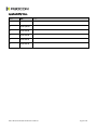
H330 LGA Serials Module Hardware User Manual Version: V1.0.7 Date: 2013-07-01 Confidential Material This document contains information highly confidential to Fibocom Wireless Inc. (Fibocom). Fibocom offers this information as a service to its customers, to support application and engineering efforts that use the products designed by Fibocom. The information provided is based upon requirements specifically provided to Fibocom by the customers. All specifications supplied herein are subject to change. Disclosure of this information to other parties is prohibited without the written consent of Fibocom. Copyright Copy, Reproduce, Distribute and/or Edit of this document or part of it as well as utilization of its contents and communication thereof to others without express authorization are prohibited. Offenders will be held liable for payment of damages. All rights created by patent grant or registration of a utility model or design patent are reserved. Copyright ©2013 Fibocom Wireless Inc. All rights reserved. Trademarks Notice The FIBOCOM Logo is registered by Fibocom Wireless Inc. All other product or service names or logos are the property of their respective owners. Copyright ©2013 Fibocom Wireless Inc. All rights reserved. Revision History Version Date Remarks V1.0.0 2012-05-30 Initial Version V1.0.1 2012-07-06 Update product model No. V1.0.2 2012-08-08 Update Mechanical, PCB Design, Pin Out V1.0.3 2012-11-26 Modify Pin description and incorrect specifications V1.0.4 2013-01-09 Update the name of the document; add reliability features V1.0.5 2013-01-24 Update the document name Update the name of the manual V1.0.6 2013-05-02 Add UART_R1 Add model comparisons Update the current specification H330 LGA Serials Module Hardware User Manual Page 2 of 41 V1.0.7 2013-07-01 Add two models Add comparison on voice H330 LGA Serials Module Hardware User Manual Page 3 of 41 Applicability Table No. Type 1 H330-Q50-00 2 H330-Q30-00 3 H330-A30-00 4 H330-A50-00 5 H330-A30-20 6 H330-A50-20 Note H330 LGA Serials Module Hardware User Manual Page 4 of 41 Contents 1 2 3 4 5 Preface ..................................................................................................................................................................................................... 7 1.1 Scope ......................................................................................................................................................................................... 7 1.2 Standards ................................................................................................................................................................................. 7 Introduction .......................................................................................................................................................................................... 8 2.1 Description .............................................................................................................................................................................. 8 2.2 Specifications ......................................................................................................................................................................... 9 2.3 Appearance ........................................................................................................................................................................... 11 Mechanical........................................................................................................................................................................................... 12 3.1 Dimensions ........................................................................................................................................................................... 12 3.2 PCB Layout Design ............................................................................................................................................................. 12 Hardware Overview .......................................................................................................................................................................... 13 4.1 Block Diagram ...................................................................................................................................................................... 13 4.2 Pin Definition........................................................................................................................................................................ 14 4.2.1 Pin Map ......................................................................................................................................................................... 14 4.2.2 Pin Description........................................................................................................................................................... 14 Hardware Interface ........................................................................................................................................................................... 20 5.1 5.2 5.3 5.4 Power Interface.................................................................................................................................................................... 20 5.1.1 VBAT ............................................................................................................................................................................... 20 5.1.2 Power Consumption ................................................................................................................................................ 20 5.1.3 VIO .................................................................................................................................................................................. 24 5.1.4 VRTC ............................................................................................................................................................................... 24 ON/OFF and Reset .............................................................................................................................................................. 25 5.2.1 Pin Definition .............................................................................................................................................................. 25 5.2.2 Power ON Signal ........................................................................................................................................................ 25 5.2.3 Power off Signal ......................................................................................................................................................... 26 5.2.4 Reset Signal ................................................................................................................................................................. 26 Indicator Signal.................................................................................................................................................................... 27 5.3.1 Pin Description........................................................................................................................................................... 27 5.3.2 Indicator Description ............................................................................................................................................... 27 USB Interface ........................................................................................................................................................................ 28 5.4.1 USB Interface Description ...................................................................................................................................... 28 H330 LGA Serials Module Hardware User Manual Page 5 of 41 5.4.2 5.5 5.6 5.7 5.8 5.9 6 7 USB Interface Application ...................................................................................................................................... 29 UART Interface ..................................................................................................................................................................... 30 5.5.1 UART Interface Description ................................................................................................................................... 30 5.5.2 UART Design ............................................................................................................................................................... 31 5.5.3 Ring Indicator ............................................................................................................................................................. 32 USIM......................................................................................................................................................................................... 32 5.6.1 USIM Interface ............................................................................................................................................................ 32 5.6.2 USIM Design................................................................................................................................................................ 33 5.6.3 USIM Design Notice ................................................................................................................................................. 33 5.6.4 USIM Hot Plug ............................................................................................................................................................ 34 Analog Audio ....................................................................................................................................................................... 34 5.7.1 Audio Interface Signal Description .................................................................................................................... 34 5.7.2 Audio Description ..................................................................................................................................................... 35 Digital Audio......................................................................................................................................................................... 36 5.8.1 I2S ................................................................................................................................................................................... 36 5.8.2 I2C ................................................................................................................................................................................... 36 Others...................................................................................................................................................................................... 37 Electrical and Environmental Features ...................................................................................................................................... 38 6.1 Electrical Features ............................................................................................................................................................... 38 6.2 Environmental Features ................................................................................................................................................... 38 RF Interface .......................................................................................................................................................................................... 39 7.1 7.2 7.3 Operation Frequency Band ............................................................................................................................................. 39 7.1.1 Main Antenna ............................................................................................................................................................. 39 7.1.2 Diversity Antenna ..................................................................................................................................................... 39 RF PCB Design ...................................................................................................................................................................... 40 7.2.1 Layout Guideline ....................................................................................................................................................... 40 7.2.2 Impedance................................................................................................................................................................... 40 Antenna Design................................................................................................................................................................... 40 7.3.1 Main Antenna Design Requirements ................................................................................................................ 40 7.3.2 Diversity Antenna Design ...................................................................................................................................... 41 H330 LGA Serials Module Hardware User Manual Page 6 of 41 1 Preface 1.1 Scope This manual provides the electrical, mechanical and environmental requirements for properly integrating the H330 serials wireless communications module. This manual gives a complete set of hardware features and functions that may be provided by H330, ensures the users can quickly and conveniently develop wireless communications using H330 Module. 1.2 Standards 3GPP TS 27.007 -v6.9.0: AT command set for User Equipment (UE) 3GPP TS 27.005 -v6.0.1: Use of Data Terminal Equipment -Data Circuit terminating Equipment (DTE-DCE) interface for Short Message Service (SMS) and Cell Broadcast Service (CBS) 3GPP TS 23.040 -v6.9.0: Technical realization of Short Message Service (SMS) 3GPP TS 24.011 -v6.1.0: Point- to - Point (PP) Short Message Service (SMS) support on mobile radio interface 3GPP TS 27.010 -v6.0.0: Terminal Equipment to User Equipment (TE-UE) multiplexer protocol 3GPP TS 27.060 -v6.0.0: Packet domain; Mobile Station (MS) supporting Packet Switched services 3GPP TS 25.304-v6.10.0: User Equipment (UE) procedures in idle mode and procedures for cell reselection in connected mode 3GPP TS 25.308 -v6.4.0: High Speed Downlink Packet Access (HSDPA); Overall description; Stage 2 3GPP TS 25.309 -v6.6.0: FDD enhanced uplink; Overall description; Stage 2 3GPP TS 23.038 -v6.1.0: Alphabets and language - specific information 3GPP TS 21.111 -v6.3.0: USIM and IC card requirements 3GPP TS 31.111 -v6.11.0 "USIM Application Toolkit (USAT)" 3GPP TS 45.002 -v6.12.0: Multiplexing and multiple access on the radio path 3GPP TS 51.014 -v4.5.0: Specification of the SIM Application Toolkit for the Subscriber Identity Module Mobile Equipment (SIM-ME) interface 3GPP TS 51.010 -1 -v6.7.0: Mobile Station (MS) conformance specification; Part 1: Conformance specification 3GPP TS 22.004 -v6.0.0: General on supplementary services 3GPP TS 23.090 -v6.1.0: Unstructured Supplementary Service Data (USSD); Stage 2 3GPP TS 24.008 v6.19, Mobile radio interface Layer 3 specification; H330 LGA Serials Module Hardware User Manual Page 7 of 41 2 Introduction 2.1 Description H330 serials are highly integrated 3G wireless communication modules, support GSM / GPRS / EDGE and UMTS / HSDPA / HSUPA / HSPA+. Here are the module comparisons: Model No. GSM/GPRS/EDGE Band(MHz) WCDMA Band(MHz) Diversity Voice HSDPA (Mbps) HSUPA (Mbps) H330-Q50-00 850/900/1800/1900 850/900/1900/2100 NO YES 21 5.76 H330-Q30-00 850/900/1800/1900 850/900/1900/2100 NO YES 7.2 5.76 H330-A30-00 900/1800 900/2100 NO YES 7.2 5.76 H330-A50-00 900/1800 900/2100 NO YES 21 5.76 H330-A30-20 900/1800 900/2100 NO NO 7.2 5.76 H330-A50-20 900/1800 900/2100 NO NO 21 5.76 Model No. Pin:3 H330-Q50-00 NC H330-Q50-05 NC H330-Q30-00 NC H330-A30-00 YES H330-A50-00 YES H330-A30-20 YES H330-A50-20 YES H330 LGA Serials Module Hardware User Manual DSP_AUDIO_IN1 Page 8 of 41 2.2 Specifications Specifications Bands UMTS (WCDMA/FDD): 850/900/1900/2100 MHz or 900/2100MHz GSM/GPRS/EDGE: 850/900/1800/1900 MHz or 900/1800MHz UMTS/HSDPA/HSUPA 3GPP release 7 HSUPA 5.76Mbps (Cat 6) Data HSDPA 21Mbps (Cat 14) or 7.2Mbps (Cat 8) GSM 3GPP release 7 EDGE (E-GPRS) multi-slot class 33 GPRS multi-slot class 33 L x W x H: 33.8mm x 27.8mm x 2.45mm Physical Interface: LGA Weight: <5.5 grams Environment Operating Temperature: -30℃ ~ +85℃ Storage Temperature: -40℃ ~ +85℃ Performance Operating Voltage Voltage: 3.3V ~ 4.2V Normal: 3.8V 2mA (Sleep Mode) Operating Current (Typical Value) 3G Idle: 13mA 3G Talk: 500mA 2G Talk: 260mA (GSM PCL5) Class 4 (2W) : 850/900 MHz, GSM Tx Power (Typical Value) Class 1 (1W) : 1800/1900 MHz, GSM Class E2 (0.5W) : 850/900 MHz, EDGE Class E2 (0.4W) : 1800/1900 MHz, EDGE Class 3 (0.25W) : 850/900/1900/2100 MHz, WCDMA Rx Sensitivity (Typical Value) UMTS/HSPA: -109dBm GSM: -108dBm Interfaces Connectors Main Antenna Diversity Antenna (some models doesn’t support) H330 LGA Serials Module Hardware User Manual Page 9 of 41 1 x USB 2.0 2 x UART MUX Over UART1 Connectivity Multiple Profiles over USB SPI Support (not supported so far) I2C Support I2S Support PCM, HSIC, GPIO, A/D, RTC Data Features Protocol Stack EDGE GPRS Embedded TCP/IP and UDP/IP protocol stack Multi-slot class 33(5 Down; 4 Up; 6 Total) Coding Scheme MCS1~9 Multi-slot class 33(5 Down; 4 Up; 6 Total) Coding Scheme CS1~4 CSD UMTS, GSM USSD Support SMS Voice Features Audio Control MO / MT Text and PDU modes Cell broadcast Analog Audio and Digital Audio Voice coders: EFR/HR/FR/AMR Gain Control, Echo Suppression, Noise Suppression, Side Tone IRA Character Set GSM UCS2 HEX FIBOCOM proprietary AT commands AT Commands GSM 07.05 GSM 07.07 Firmware Loader Tool over USB/UART Accessories User Manual Developer Kit H330 LGA Serials Module Hardware User Manual Page 10 of 41 2.3 Appearance The following picture shows the H330 Wireless Communication Module. Top view: Figure 2-1 Bottom view: Figure 2-2 H330 LGA Serials Module Hardware User Manual Page 11 of 41 3 Mechanical 3.1 Dimensions Figure 3-1 3.2 PCB Layout Design Figure 3-2 H330 LGA Serials Module Hardware User Manual Page 12 of 41 4 Hardware Overview 4.1 Block Diagram Figure 4-1 H330 LGA Serials Module Hardware User Manual Page 12 of 40 4.2 Pin Definition 4.2.1 Pin Map TOP (View) Figure 4-2 4.2.2 Pin Description The logic electrical lever of H330 is 1.8V. The following table shows H330 pin description: Pin# Pin Name I/O Description Power Supply 59 VBAT I 60 VBAT I 61 VBAT I 62 VBAT I 64 VPA O Power supply indicator for RF PA 1 VTRX O Power supply indicator for RF transceiver 46 VIO O 1.8V voltage output inside module 47 VRTC I/O Backup battery power input. Module main power input, voltage range: 3.3V ~ 4.2V H330 LGA Serials Module Hardware User Manual Page 14 of 41 Power ON/OFF Signal 48 POWER_OFF I Power off signal 49 POWER_ON I Power on signal RESET_ALL_N I External reset signal 4 USIM_CD I USIM card insert detected. Low activity 5 USIM_VCC O USIM card supplies the power, 1.8V or 3.3V 6 USIM_RST O USIM card reset 7 USIM_CLK O USIM card clock 8 USIM_DATA I/O USIM card data Reset Signal 77 USIM High Speed SIM 9 USIM_D+ High Speed SIM card USB data line+ (not supported) 10 USIM_D- High Speed SIM card USB data line- ( not supported) Audio 13 AUXO+ O Speaker output signal+ 14 AUXO- O Speaker output signal- 15 EAR- O Earphone output signal - 16 EAR+ O Earphone output signal+ 17 MIC+ I Main MIC input signal + 18 MIC- I Main MIC input signal- 19 AUXI- I Auxiliary MIC input signal - 20 AUXI+ I Auxiliary MIC input signal + 21 AGND GND Audio GND 22 VSPK I Audio codec speaker part power supply, connect to VBAT I 2S H330 LGA Serials Module Hardware User Manual Page 15 of 41 11 I2S2_CLK1 O I2S2 Clock SCLK1 24 I2S2_CLK0 O I2S2 l Clock SCLK0 (I2S2 use CLK0 by default) 25 I2S2_WA0 O I2S2 word alignment select 26 I2S2_TX O I2S2 transmit line 27 I2S2_RX I I2S2 receive line 31 USB_DP I/O USB data line+ 32 USB_DM I/O USB data line- 33 USB_ID — USB ID line 34 VUSB I USB Power Input 92 USB_TEST — USB TEST line 28 I2C_SDA I/O I2C data line 29 I2C_SCL O I2C clock line 35 UART1_RI O UART1 Ring Indicator 36 UART1_DSR I UART1 DTE Ready 37 UART1_DTR O UART1 DCE Ready 38 UART1_DCD O UART1 Carrier Detect 39 UART1_CTS I UART1 Clear To Send 40 UART1_RTS O UART1 Request To Send 41 UART1_TXD O UART1 Transmitted Data 42 UART1_RXD I UART1 Received Data 45 UART2_TXD O UART2 Transmitted Data 44 UART2_RXD I UART2 Received Data USB I 2C UART1 UART2 H330 LGA Serials Module Hardware User Manual Page 16 of 41 ADC 50 ADC2 Analog digital converter 2 ( not supported) 51 ADC1 Analog digital converter 1 ( not supported) EINT 56 WAKE_UP I External wake-up interrupt, Low activity. 57 EINT2 I External interrupt, Low activity. USB HSIC 90 HSIC_USB_DATA HSIC USB data signal ( not supported) 91 HSIC_USB_STRB HSIC USB pulse signal ( not supported) Antenna 67 ANT_MAIN I Main antenna interface, 50 ohm Impedance 71 ANT_DIV I Only supported by some models Others 1. DSP audio input 3 DSP_AUDIO_IN1 I 54 CLKOUT0 O Digital audio clock output 89 SMI I Sleep Mode Indicator 86 LPG O Status Indicator 2. GPIO: only supported by some models Not Connect 23 NC 55 NC 52 NC 53 NC 73 NC 74 NC 75 NC H330 LGA Serials Module Hardware User Manual Page 17 of 41 76 NC 78 NC 79 NC 80 NC 81 NC 82 NC 83 NC 84 NC 85 NC 87 NC 88 NC 94 NC 95 NC 96 NC 101 NC 105 NC 106 NC 107 NC 108 NC GND 2 GND 12 GND 30 GND 43 GND 58 GND 63 GND H330 LGA Serials Module Hardware User Manual Page 18 of 41 65 GND 66 GND 68 GND 69 GND 70 GND 72 GND 93 GND 97 GND 98 GND 99 GND 100 GND 102 GND 103 GND 104 GND 109 GND 110 GND 111 GND 112 GND 113 GND 114 GND 115 GND 116 GND 117 GND 118 GND 119 GND 120 GND H330 LGA Serials Module Hardware User Manual Page 19 of 41 5 Hardware Interface 5.1 Power Interface 5.1.1 VBAT H330 module requires a 3.3 V~ 4.2V DC power supply to provide 2A as GSM transmitter maximum current. Input power supply requirements: Parameter Minimum Value Recommended Value Maximum Value Unit VBAT 3.3 3.8 4.2 V Note: 1. Supply voltage fluctuations need to be lower than 300mV. 2. Supply voltage drop minimum value needs to be higher than 3.3V. Filter capacitor description: Recommended capacitor Application Description 1000uF GSM Transmit current serge Minimizes power supply losses during transmit bursts. Use maximum possible value. 10nF, 100nF Digital signal to noise Filtering interference from clock and data sources 8.2pF, 10pF 1800/1900/2100 MHz GSM bands Filters transmission EMI. 33pF, 39pF 850/900 MHz GSM bands Filters transmission EMI. 5.1.2 Power Consumption Parameter Description I off RTC mode I idle Idle mode I sleep I GSM-RMS Low power mode GSM voice 1 TX slot 1 Rx slot Condition Typical Value Unit 60 uA GSM 13 mA WCDMA 13 mA DRX 2 2 DRX 5 2 DRX 9 2 5 230 10 80 GSM850 PCL H330 LGA Serials Module Hardware User Manual mA mA Page 20 of 41 15 50 19 46 5 240 10 83 15 50 19 47 0 156 5 71 10 49 15 46 0 165 5 70 10 50 15 46 5 355 10 216 15 108 19 94 5 383 10 225 EGSM900 PCL DCS1800 PCL PCS1900 PCL GSM850 PCL I GPRS-RMS GPRS Class 33 4 TX slot 1 Rx slot EGSM900 PCL mA 15 108 19 94 0 259 5 180 10 103 15 95 DCS1800 PCL H330 LGA Serials Module Hardware User Manual Page 21 of 41 0 266 5 182 10 103 15 95 8 522 14 145 19 95 8 522 14 150 19 95 PCS1900 PCL GSM850 PCL EGSM900 PCL I EGPRS-RMS EGPRS Class 33 4 TX slot 1 Rx slot mA DCS1800 PCL PCS1900 PCL 2 484 9 117 15 103 2 493 9 118 15 103 5 1655 10 473 15 193 19 148 5 1715 10 536 15 208 19 147 0 1050 5 464 GSM850 PCL I GSM-MAX Peak current During TX slot mA EGSM900 PCL DCS1800 PCL H330 LGA Serials Module Hardware User Manual Page 22 of 41 10 199 15 138 0 1100 5 489 10 203 15 139 24dBm 387 0dBm 127 -24dBm 121 -50dBm 119 24dBm 439 0dBm 130 -24dBm 123 -50dBm 121 PCS1900 PCL Band5 (850) Band2 (1900) I WCDMA-RMS mA WCDMA 24dBm 475 0dBm 131 -24dBm 121 -50dBm 119 24dBm 384 0dBm 127 -24dBm 123 -50dBm 121 Band1 (2100) Band8 (900) H330 LGA Serials Module Hardware User Manual Page 23 of 41 5.1.3 VIO VIO is power supply for the digital portion of the circuit inside of the module; it can be used for indicating signal of the module. VIO can be used as a reference level of the module digital signal. Parameter Minimum Value Recommended Value Maximum Value Unit VIO @working 1.773 1.8 1.827 V 5.1.4 VRTC VRTC supplies power for RTC clock inside the module, can be connected to external RTC battery. Parameter Minimum Value Recommended Value Maximum Value Unit VRTC output voltage 1.71 1.8 1.89 V 0.5 1.8 1.89 V 1.5 uA VRTC input voltage (RTC is working) VRTC input current (RTC is working) VRTC Reference design: Figure 5-1 Note: R8 is the current-limiting resistance in order to ensure VRTC working normally. When it is working fine, R8>1kohm VRTC Current consumption < 2uA; C9 value can affect RTC hold time H330 LGA Serials Module Hardware User Manual Page 24 of 41 5.2 ON/OFF and Reset 5.2.1 Pin Definition H330 wireless communication module has three control signals: power on, off and reset the module. Pin Definition: Pin# Pin Name Electrical Level Description 48 POWER_OFF CMOS 1.8V Power off signal 49 POWER_ON CMOS 1.8V Power on signal 77 RESET_ALL_N CMOS 1.8V External reset signal input 5.2.2 Power ON Signal After the module is powered on, users can lower down the POWER_ON signal, then module boots up. The following table shows the burst timing: Parameter Condition Pulse Width Minimum Value Typical Value Maximum Value Unit 100 300 3000 ms Timing control: VBAT 3S POWER_ON 300mS VDD_1V8 8mS Figure 5-2 Reference design: Figure 5-3 H330 LGA Serials Module Hardware User Manual Page 25 of 41 5.2.3 Power off Signal After lower down POWER_OFF signal, module changes to shutdown status. Parameter Condition Pulse Width Minimum Value Typical Value Maximum Value Unit 100 300 3000 ms Timing control: Figure 5-4 Reference design: Figure 5-5 5.2.4 Reset Signal H330 wireless communication module supports external reset; it can restore the module to default settings through Reset signal. When Reset signal is Active Low by 100ms, the module will reset. When users reset the module, PMU inside the module is still on. If the module is connected to PC, you can see PC Virtual port restarts. Note: Reset signal is sensitive, when PCB layout, please keep it away from radio frequency interference, add debouncing capacitor near the module end is recommended. H330 LGA Serials Module Hardware User Manual Page 26 of 41 Parameters Condition Pulse Width Minimum Value Typical Value Maximum Value Unit 100 300 3000 ms Recommended design: Figure 5-6 5.3 Indicator Signal 5.3.1 Pin Description Pin# Pin Name Description 86 LPG Work mode indicator 89 SMI Sleep Mode Indicator 56 WAKE_UP Wake up module 1 VTRX Power supply indicator for transceiver 64 VPA Power supply indicator for RF PA 5.3.2 Indicator Description 5.3.2.1 LPG Signal LPG signal description: Status Mode idle(unregistered) 600ms high level, 600ms low level idle(registered) 75ms high level, 3S low level Call low level Data communicating 75ms high level, 75ms low level Sleep high level H330 LGA Serials Module Hardware User Manual Page 27 of 41 Note: High level voltage is 1.8V. 5.3.2.2 SMI Module Mode Mode Sleep Mode 2.5S High; 100ms Low Other Mode low level 5.3.2.3 WAKE_UP Module Mode WAKE_UP Signal Description Low level Wake up module, switch from Sleep to Idle High level Stay in Sleep mode Low level Keep mode, no affect High level Module cannot set to Sleep mode Sleep Idle/Call 5.3.2.4 Others Pin Name Electrical Level Description VTRX 1.8V RF Transceiver PMU work indicator VPA 0-4.3V It works in Tx mode, when the low power it is about 0.65V, when the max. power it is about 4.3V, other mode it is 0V Note: Only Indicates signal. 5.4 USB Interface 5.4.1 USB Interface Description Pin# Pin Name I/O Description 31 USB_DP I/O USB signal+ 32 USB_DM I/O USB signal- 33 USB_ID — USB ID signal 34 VUSB I USB power input 92 USB_TEST — USB TEST signal H330 wireless communication module supports USB 2.0. Install the corresponding USB driver before use on PC. H330 LGA Serials Module Hardware User Manual Page 28 of 41 After H330 wireless communication module plugged into the PC, the USB can map seven ports: One 3G Modem port, for data operation Two ports for sending AT Command Two ports for trace Two ports are reserved 5.4.2 USB Interface Application Reference Design: Figure 5-7 T101 and T102 should be low capacitor TVS, it is below 1 pF. VUSB is USB power supply, Recommend power supply range is 2.5V ~ 5.25V. VUSB should be connect to a level (2.5V ~ 5.25V) or USB cannot be recognized. USB_DP and USB_DM are high speed lines, the highest transmit speed is 480 Mbps. PCB Layout notice: Note: USB_DP and USB_DM lines need equal length, parallel, as short as possible. The input and output need GND isolation. The layout design of this circuit on the AP board should comply with the USB 2.0 high speed protocol, with differential lining and impedance control to 90 ohm. H330 LGA Serials Module Hardware User Manual Page 29 of 41 5.5 UART Interface 5.5.1 UART Interface Description H330 wireless communication module provides two UART, one is 8 wire serial bus interface, and the other is a 2 wire serial bus interface. 8 wire serial bus interface (UART1) supports flow control; users can download software or send/receive AT through UART1. 2 wire serial bus interface (UART2) supports a few AT Commands. Note: UART2 only supports some common query functions. UART1 and UART2 signal description: UART1 Pin# Pin Name I/O Description 35 UART1_RI O UART1 Ring Indicator 36 UART1_DSR I UART1 DTE Ready 37 UART1_DTR O UART1 DCE Ready 38 UART1_DCD O UART1 Carrier Detect 39 UART1_CTS I UART1 Clear to send 40 UART1_RTS O UART1 Request to send 41 UART1_TXD O UART1 Transmitted Data 42 UART1_RXD I UART1 Received Data Pin# Pin Name I/O Description 44 UART2_RXD I UART2 Transmitted Data 45 UART2_TXD O UART2 Received Data UART2 H330 LGA Serials Module Hardware User Manual Page 30 of 41 5.5.2 UART Design The following table show the signal direction when H330 wireless communication module (DCE) UART1 connects to PC (DTE): Application MCU(DTE) Signal Direction H330 Module (DCE) RXD UART1_TXD TXD UART1_RXD RTS UART1_CTS CTS UART1_RTS DSR UART1_DTR DTR UART1_DSR RI UART1_RI DCD UART1_DCD The following table shows the signal direction when H330 wireless communication module (DCE) UART2 connects to PC (DTE): Application MCU(DTE) Signal Direction H330 Module (DCE) RXD UART2_TXD TXD UART2_RXD Note: H330 wireless communication module UART high level is 1.8V, please use external level shifter if connect to 2.8V or 3.3V IO interface. When design: Level shift from 1.8V to 3.3V, SN74LVC2G07 is recommended. When UART1 communicating with PC, first shift from 1.8V to 3.3V, and then uses SP3238 to shift. When UART2 communicating with PC, first shift from 1.8V to 3.3V, and then uses SPIEX3232EEA to shift level. Notice the signal direction when shift level. H330 LGA Serials Module Hardware User Manual Page 31 of 41 5.5.3 Ring Indicator UART1_R1 is used for indicating incoming call and SMS, sending pulse to host application program. Module Mode Status No ringing Low level Ringing 1s high level, 1s low level, cycling No message Low level Incoming message 150ms pulse 5.6 USIM H330 wireless communication module supports USIM and high speed SIM card, does not support 8 line smart USIM yet. 5.6.1 USIM Interface Pin# Pin Name I/O Description 5 USIM_VCC O USIM power supply output 6 USIM_RST O USIM Reset signal 7 USIM_CLK O USIM clock signal 8 USIM_IO I/O USIM data signal 12 GND GND USIM ground USIM insert detect signal 4 USIM_CD I High level indicates SIM card is not inserted Low level indicates SIM card is inserted H330 LGA Serials Module Hardware User Manual Page 32 of 41 5.6.2 USIM Design Reference design: Figure 5-8 Note: For better EMC performance, SIM card position should be close to module Filtering capacitor should be close to SIM card pin The interface need add ESD protection, ESD should be close to SIM card pin USIM_IO is already pulled up inside the module, USIM_CD support SIM hot plug, low level is effective, if low level is detected, this means SIM card is inserted. 5.6.3 USIM Design Notice The SIM interface and signals design is extremely important for proper operation of the SIM card. There are several design guidelines that must be followed: The layout signals of the SIM card should be away from any possible EMI interference sources, such as the RF antenna and digital switching signals. To ensure signal integrity, the length between SIM interface signals and module should not exceed 100 mm To avoid crosstalk between USIM_CLK and USIM_IO, it is recommended to route them separately on the application board, and preferably isolated by a surrounding ground plane. The SIM card signals should be protected from ESD using very low capacitance protective elements (like Zener diode). The recommended part no of ESD is AVR-M1005C080MTAAB (TDK). ESD component should layout with SIM hold closely. H330 LGA Serials Module Hardware User Manual Page 33 of 41 5.6.4 USIM Hot Plug H330 supports SIM hot plug. 5.6.4.1 Hardware Connection SIM hot plug function interacts with USIM_CD signal. When no SIM card, USIM_CD is high level; insert SIM, USIM_CD is low level. In reference design USIM_CD connect U3 Pin8 (SW2), Pin7 (SW1) connect GND. When no SIM card, SW2 is high level; Insert SIM, SW2 connect SW1,USIM_CD is pulled down 5.6.4.2 Software Design “+MSMPD” AT command defines the SIM card status detection feature. When set AT+MSMPD=0, the SIM detected feature deactivated. Module does not detect USIM_CD signal. When set AT+MSMPD=1, the SIM detected feature activated. USIM_CD pin can test whether SIM card is onsite or not. SIM_CD is Low level, SIM card is onsite, and module registers the network automatically. SIM_CD is High level or not connected, SIM card is offsite and module drops out the network. Note: The +MSMPD default value is “0”. 5.7 Analog Audio 5.7.1 Audio Interface Signal Description The H330 audio interface supports two channel audio signals input and two channel audio signal output. Pin# Pin Name I/O Description 13 AUXO+ O Audio channel2 output + 14 AUXO- O Audio channel2 output - 15 EAR- O Audio channel1 earphone signal output- 16 EAR+ O Audio channel1 earphone signal output+ 17 MIC+ I Audio channel1 MIC signal input+ 18 MIC- I Audio channel1 MIC signal input- 19 AUXI- I Audio channel2 MIC signal input - 20 AUXI+ I Audio channel2 MIC signal input + 21 AGND GND Audio GND 22 VSPK I Audio codec speaker part power supply, connect to VBAT H330 LGA Serials Module Hardware User Manual Page 34 of 41 5.7.2 Audio Description The audio input and output channels are differential interfaces. And have prefect performance at RF Spurious suppression. When connect to the handset, need external audio amplifier. In PCB Layout, the differential lines need equal length, parallel, as short as possible, for a better performance, the input and output need GND Isolation and the interface need to add ESD protection. 5.7.2.1 Audio Channel 1 Audio channel 1 interface use differential lines, it can be used for handling calls Audio channel 1:MIC input characteristic: Parameter Test conditions Bias voltage No load Gain Programmable, steps gain:2dB Minimum Value Typical Value Maximum Value Unit 2.5 2.6 V 16 dB 0 Load resistance 2.2 Kohm Audio channel 1:EAR output characteristic: Parameter Test conditions Output voltage No load Minimum Value Typical Value Maximum Value Unit 1.4 Vpp Load resistance 32 ohm DC Bias voltage 1 V 5.7.2.2 Audio Channel 2 Audio channel 2 interface use differential lines, Can be use as Hands-free. Note: The downstream of Audio channel 2 cannot work until VSPK power supply is normal. The VSPK can be straight connected to VBAT. Audio channel 2: AUXI input characteristic: Parameter Test conditions Bias voltage No load Gain Programmable, steps gain:2dB Load resistance H330 LGA Serials Module Hardware User Manual Minimum Value Typical Value Maximum Value Unit 2.5 2.6 V 32 dB 0 2.2 Kohm Page 35 of 41 Audio channel 2: AUXO output characteristic: Parameter Test conditions Out voltage No load Minimum Value Load resistance Typical Value Maximum Value Unit 3.8 Vpp 8 ohm 5.8 Digital Audio Digital audio signal description: Pin# Pin Name I/O Description 24 I2S2_CLK0 O Bit Clock 25 I2S2_WA0 O Frame clock(LRCK) 26 I2S2_TX O Serial data output 27 I2S2_RX I Serial data input 28 I2C_DATA I/O I2C data line 29 I2C_SCL O I2C clock line 54 CLKOUT0 O 26MHz clock output 5.8.1 I2S H330 Signal Direction Audio CODEC I2S Port I2S2_CLK0 I2S_CLK I2S2_WA0 I2S_LRCK I2S2_RX I2S_SDIN I2S2_TX I2S_SDOUT CLKOUT0 I2S_MCLK 5.8.2 I2C H330 Signal Direction Audio CODEC I2C Port I2C_SDA I2C_SDA I2C_SCL I2C_SCL H330 LGA Serials Module Hardware User Manual Page 36 of 41 Note: I2S can work in master mode or slave mode It supports many audio sample rates (48 KHz, 44.1 KHz, 32 KHz, 24 KHz, 22.5 KHz, 16 KHz, 12 KHz, 11.025 KHz and 8 KHz). 5.9 Others The module does not support interface like GPIO、MIPI、MMC、DAC yet. H330 LGA Serials Module Hardware User Manual Page 37 of 41 6 Electrical and Environmental Features 6.1 Electrical Features This table shows the electrical features range of H330. Parameter Minimum Value Maximum Value Unit VBAT 0 4.2 V Digital Signal 0 1.9 V 6.2 Environmental Features This table shows the environmental features of H330. Parameter Minimum Value Maximum Value Unit Operational Temperature -30 +85 °C Storage Temperature -40 +85 °C H330 LGA Serials Module Hardware User Manual Page 38 of 41 7 RF Interface Please refer to the model comparisons in chapter 2 for more information. 7.1 Operation Frequency Band 7.1.1 Main Antenna Operating Band Tx Rx 1920–1980 MHz 2110–2170 MHz UMTS 1900 (Band II PCS) 1850–1910 MHz 1930–1990 MHz UMTS 850 (Band V CLR) 824–849 MHz 869–894 MHz UMTS 900 (Band VIII GSM) 880–915 MHz 925–960 MHz GSM 850 824–849 MHz 869–894 MHz GSM 900 880–915 MHz 925–960 MHz DCS 1800 1710–1785 MHz 1805–1880 MHz PCS 1900 1850–1910 MHz 1930–1990 MHz UMTS 2100 (Band I IMT) 7.1.2 Diversity Antenna Operating Band Rx UMTS 2100 (Band I IMT) 2110–2170 MHz UMTS 1900 (Band II PCS) 1930–1990 MHz UMTS 850 (Band V CLR) 869–894 MHz UMTS 900 (Band VIII GSM) 925–960 MHz H330 LGA Serials Module Hardware User Manual Page 39 of 41 7.2 RF PCB Design 7.2.1 Layout Guideline As H330 does not have a RF connector, so for RF line, microstrip line is recommended. The shorter the better, insert loss is less than 0.2dB; impedance is less than 50ohm. It is recommended to mount H330 module and antenna connector to the same side of layout. Add a π-type circuit (two parallel device ground pin directly to the main land) for antenna matching. Figure 7-1 7.2.2 Impedance The RF lines impedance should not exceed 50 ohm. 7.3 Antenna Design 7.3.1 Main Antenna Design Requirements (1) Antenna Efficiency Antenna efficiency is the ratio between antenna input power and radiation power. The radiation power of an antenna is always lower than the input power due to the following factors: return loss, material loss, and coupling loss. Efficiency of the master antenna > 40% (–4dB) (2) S11 or VSWR S11 (return loss) indicates the degree to which the input impedance of an antenna matches the reference impedance (50 ohm). S11 shows the resonance feature and impedance bandwidth of an antenna. Voltage standing wave ratio (VSWR) is another expression of S11. S11 relates to the antenna efficiency. S11 can be measured by vector analyzer. S11 of the master antenna < –10 dB (3) Polarization The polarization of an antenna is the orientation of the electric field vector that rotates with time in the direction of maximum radiation. Linear polarization is recommended: it would be better if the polarization direction of diversity antenna is different from main antenna. H330 LGA Serials Module Hardware User Manual Page 40 of 41 (4) Radiation Pattern Radiation pattern refers to the directional dependence of the strength of the radio waves from the antenna or other source. The radiation pattern of half wave dipole antennas is the best for wireless terminals. If it is built-in antenna, PIFA antenna is recommended: Antenna area (H x W x L): 6mm x 10mm x 100mm. PIFA or IFA antenna is recommended. Radiation Pattern: Omni directional (5) Gain and Directivity The directivity of the antenna is the electromagnetic field strength of the electromagnetic wave in each direction. An antenna's power gain is a key performance figure which combines the antenna’s directivity and electrical efficiency. Recommended antenna gain ≤ 2.5dBi (6) Interference Besides the antenna performance, the interference on the PCB board also affects the radio performance (especially the TIS) of the module. To guarantee high performance of the module, the interference sources on the user board must be properly controlled. On the PCB board, there are various interference sources that can affect the module, such as the speaker, LCD, CPU, FPC trace and audio circuits, the power supply should be far away from antenna, notice isolation, shield and filtering processing issues. (7) TRP/TIS TRP (Total Radiated Power): W850/W900/W1900/W2100>19dBm GSM850>28dBm GSM900>28dBm DCS1800>25dBm PCS1900>25dBm TIS (Total Isotropic Sensitivity) : W850/W900<-102dBm W1700/W1900/W2100<-103dBm GSM850<-102dBm GSM900<-102dBm DCS1800/PCS1900<-102dBm 7.3.2 Diversity Antenna Design Diversity reception function of H330 is optional, please add a diversity antenna if you want to use this function. The design methods of diversity antenna and main antenna are the same, its efficiency indicators allows to reduce 3dB. The isolation between main antenna and diversity antenna should be higher than 12dB. H330 LGA Serials Module Hardware User Manual Page 41 of 41