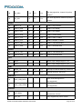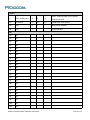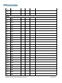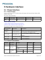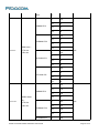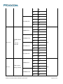
1
H330S LGA Series Module Hardware User Manual Version:V1.1.5 Date:2015.09.22 第 1 页 共 45 页 Copyright Copyright ©2015 Fibocom Wireless Inc . All rights reserved. Without the prior written permission of the copyright holder, any company or individual is prohibited to excerpt, copy any part of or the entire document, or transmit the document in any form. Attention The document is subject to update from time to time owing to the product version upgrade or other reasons. Unless otherwise specified, the document only serves as the user guide. All the statements, information and suggestions contained in the document do not constitute any explicit or implicit guarantee. Trademark The trademark is registered and owned by Fibocom Wireless Inc. Versions Version Date Remarks V1.0.0 2012-05-30 Initial Version V1.0.1 2012-07-06 Update product model No. V1.0.2 2012-08-08 Update Mechanical, PCB Design, Pin Out V1.0.3 2012-11-20 Modify Pin description and incorrect specifications V1.0.4 2013-01-09 Update the name of the document; add reliability features V1.0.5 2013-01-24 Update the document name Update the name of the manual V1.0.6 2013-05-02 Add UART_R1 Add model comparisons Update the current specification V1.0.7 2013-07-01 V1.0.8 2013-09-13 Add two models Add comparison on voice SMI is updated to a output pin; update section 5.4.1; Update Figure5-2, Figure5-4; H330S LGA Serials Module Hardware User Manual Page 2 of 45 Update description of RTC Add section 5.8.3 Update section 5.3.2.3 WAKE_UP V1.0.9 2013-10-12 Update description for ADC, POWER OFF and RESET. Modify I2S signal Pin # in section 5.8. V1.1.0 2013-12-18 Add default status and idle status of GPIO Update downstream rate and upstream rate of GPRS Update the maximum operating voltage to 4.5V V1.1.1 2015-01-30 Update the range of operating temperature. V1.1.2 2015-04-21 Add the description of “Top View” in PCB Layout V1.1.3 2015-05-10 V1.1.4 2015-07-27 Update the info of H330S and the logo. V1.1.5 2015-09-22 Update the 12C and 12S description of H330S-XXX-20 Update the description of copyright and attention. Update the translation of the whole document. H330S LGA Serials Module Hardware User Manual Page 3 of 45 Applicability Type No. Type Note 1 H330S-Q50-00 2 H330S-Q30-00 3 H330S-A30-00 4 H330S-A50-00 5 H330S-A30-20 6 H330S-A50-20 仅有 MiniPCIe 型号 7 H330S-Q50-20 仅有 MiniPCIe 型号 The difference of H330S series wireless module as listed below: Model No. GSM/GPRS/EDGE Band(MHz) WCDMA Band(MHz) Voice HSDPA HSUPA (Mbps) (Mbps) H330S-Q50-00 850/900/1800/1900 850/900/1900/2100 Y 21 5.76 H330S-Q30-00 850/900/1800/1900 850/900/1900/2100 Y 7.2 5.76 H330S-A30-00 900/1800 900/2100 Y 7.2 5.76 H330S-A50-00 900/1800 900/2100 Y 21 5.76 H330S-A30-20 900/1800 900/2100 N 7.2 5.76 H330S-A50-20 900/1800 900/2100 N 21 5.76 H330S-Q50-20 850/900/1800/1900 850/900/1900/2100 N 21 5.76 H330S LGA Serials Module Hardware User Manual Page 4 of 45 Contents 1 Foreword..................................................................................................................................................................... 8 1.1 Introduction..................................................................................................................................................... 8 1.2 Reference Standards.................................................................................................................................... 8 2 Product Overview...................................................................................................................................................... 9 2.1 Description...................................................................................................................................................... 9 2.2 Specifications................................................................................................................................................. 9 2.3 Appearance...................................................................................................................................................12 3 Structure................................................................................................................................................................... 13 3.1 Dimension Diagram of Structure............................................................................................................... 13 3.2 PCB Layout Design..................................................................................................................................... 13 4 Hardware Introduction............................................................................................................................................ 14 4.1 Hardware Block Diagram........................................................................................................................... 14 4.2 Pin Definition.................................................................................................................................................15 4.2.1 Pin Map.............................................................................................................................................. 15 4.2.2 Description of Pins........................................................................................................................... 16 5 Hardware Interface................................................................................................................................................. 22 5.1 Power Interface............................................................................................................................................ 22 5.1.1 Power Supply.................................................................................................................................... 22 5.1.2 Power Consumption.........................................................................................................................22 5.1.3 VIO...................................................................................................................................................... 26 5.1.4 VRTC.................................................................................................................................................. 26 5.2 Power on/off and Reset Signal.................................................................................................................. 27 5.2.1 Pin Definition of Power on/off Control Signal.............................................................................. 27 5.2.2 Power on Signal............................................................................................................................... 27 5.2.3 Power off Signal............................................................................................................................... 28 5.2.4 Reset Signal...................................................................................................................................... 28 5.3 Status Indicating Signal.............................................................................................................................. 30 5.3.1 LPG Signal........................................................................................................................................ 30 5.3.2 SMI Signal......................................................................................................................................... 30 H330S LGA Serials Module Hardware User Manual Page 5 of 45 5.3.3 WAKE_UP Signal............................................................................................................................. 30 5.3.4 Other Work Indications.................................................................................................................... 31 5.4 USB Interface............................................................................................................................................... 32 5.4.1 USB Interface Definition.................................................................................................................. 32 5.4.2 USB Interface Application............................................................................................................... 32 5.5 UART Interface.............................................................................................................................................34 5.5.1 UART Interface Description............................................................................................................ 34 5.5.2 UART Interface Application............................................................................................................ 34 5.5.3 Ring Indication.................................................................................................................................. 35 5.6 USIM Interface............................................................................................................................................. 36 5.6.1 USIM Pins.......................................................................................................................................... 36 5.6.2 USIM Design..................................................................................................................................... 36 5.6.3 Points for Attention in USIM Design..............................................................................................37 5.6.4 USIM Hot-Plugging.......................................................................................................................... 37 5.7 Analog Audio Interface............................................................................................................................... 38 5.7.1 Definition of Audio Interface Signals............................................................................................. 38 5.7.2 Description of Audio Interface Application................................................................................... 38 5.8 Digital Audio.................................................................................................................................................. 40 5.8.1 I2S....................................................................................................................................................... 40 5.8.2 I2C.......................................................................................................................................................40 5.8.3 PCM Port Description...................................................................................................................... 41 5.9 ADC Interface............................................................................................................................................... 41 5.10 Other Interfaces......................................................................................................................................... 41 6 Electrical and Environmental Features................................................................................................................42 6.1 Electrical Features....................................................................................................................................... 42 6.2 Environmental Features............................................................................................................................. 42 7 RF Interface..............................................................................................................................................................43 7.1 Operating Frequency Band........................................................................................................................ 43 7.1.1 Frequency Range of Main Antenna.............................................................................................. 43 7.2 RF PCB Design............................................................................................................................................ 43 7.2.1 Wiring Principle................................................................................................................................. 43 H330S LGA Serials Module Hardware User Manual Page 6 of 45 7.2.2 Impedance Design........................................................................................................................... 44 7.3 Antenna Design............................................................................................................................................44 7.3.1 Main Antenna Design Requirements............................................................................................ 44 H330S LGA Serials Module Hardware User Manual Page 7 of 45 1 Foreword 1.1 Introduction The document describes the electrical characteristics, RF performance, dimensions and application environment, etc. of H330S series wireless modules. With the assistance of the document and other instructions, developers can quickly understand the performance of H330S series wireless modules and develop products. 1.2 Reference Standards The design of the product complies with the following standards: 3GPP TS 27.007 -v6.9.0: AT command set for User Equipment (UE) 3GPP TS 27.005 -v6.0.1: Use of Data Terminal Equipment -Data Circuit terminating Equipment (DTE-DCE) interface for Short Message Service (SMS) and Cell Broadcast Service (CBS) 3GPP TS 23.040 -v6.9.0: Technical realization of Short Message Service (SMS) 3GPP TS 24.011 -v6.1.0: Point- to - Point (PP) Short Message Service (SMS) support on mobile radio interface 3GPP TS 27.010 -v6.0.0: Terminal Equipment to User Equipment (TE-UE) multiplexer protocol 3GPP TS 3GPP TS 25.304-v6.10.0: User Equipment (UE) procedures in idle mode and procedures for cell 27.060 -v6.0.0: Packet domain; Mobile Station (MS) supporting Packet Switched services reselection in connected mode 3GPP TS 25.308 -v6.4.0: High Speed Downlink Packet Access (HSDPA); Overall description; Stage 2 3GPP TS 25.309 -v6.6.0: FDD enhanced uplink; Overall description; Stage 2 3GPP TS 23.038 -v6.1.0: Alphabets and language - specific information 3GPP TS 21.111 -v6.3.0: USIM and IC card requirements 3GPP TS 31.111 -v6.11.0 "USIM Application Toolkit (USAT)" 3GPP TS 45.002 -v6.12.0: Multiplexing and multiple access on the radio path 3GPP TS 51.014 -v4.5.0: Specification of the SIM Application Toolkit for the Subscriber Identity Module - Mobile Equipment (SIM-ME) interface 3GPP TS 51.010 -1 -v6.7.0: Mobile Station (MS) conformance specification; Part 1: Conformance specification 3GPP TS 22.004 -v6.0.0: General on supplementary services 3GPP TS 23.090 -v6.1.0: Unstructured Supplementary Service Data (USSD); Stage 2 3GPP TS 24.008 v6.19, Mobile radio interface Layer 3 specification; H330S LGA Serials Module Hardware User Manual Page 8 of 45 2 Product Overview 2.1 Description H330S series modules are 3G wireless modules with high integration density, supporting GSM/GPRS/ EDGE and UMTS/HSDPA/HSUPA/HSPA+. 2.2 Specifications Specifications Operating UMTS (WCDMA/FDD): 850/900/1900/2100 MHz or 900/2100MHz Frequency Range GSM/GPRS/EDGE: 850/900/1800/1900 MHz or 900/1800MHz UMTS/HSDPA/HSUPA 3GPP release 7 HSUPA 5.76Mbps (Cat 6) HSDPA 21Mbps (Cat 14) or 7.2Mbps (Cat 8) Data Rate GSM 3GPP release 7 EDGE (E-GPRS) multi-slot class 33 (296kbps DL, 236.8kbps UL) GPRS multi-slot class 33 (107kbps DL, 85.6kbps UL) Dimension: 33.8 x 27.8 x 2.45mm Physical Characteristics Interface: LGA Weight: <5.5 grams Normal operating Temperature: -30℃ ~ +75℃ Environment ① Restricted operating temperature : -40℃ ~ +85℃ Storage Temperature: -40℃ ~ +85℃ Performance Operating Voltage Voltage: 3.3V ~ 4.5V Normal: 3.8V 2mA (Sleep Mode) Current 3G Idle: 13mA Consumption (Typical Value) 3G Talk: 500mA 2G Talk: 260mA (GSM PCL5) H330S LGA Serials Module Hardware User Manual Page 9 of 45 Class 4 (2W) : 850/900 MHz, GSM Class 1 (1W) : 1800/1900 MHz, GSM Tx Power (Typical Value) Class E2 (0.5W) : 850/900 MHz, EDGE Class E2 (0.4W) : 1800/1900 MHz, EDGE Class 3 (0.25W) : 850/900/1900/2100 MHz, WCDMA Rx Sensitivity UMTS/HSPA: -109dBm (Typical Value) GSM: -108dBm Interfaces Rf Interface Main Antenna 1 x USB 2.0 2 x UART MUX Over UART1 Function Multiple Profiles over USB Interface SPI Support (Not supported yet) I2C Support I2S Support ② ② PCM, HSIC, GPIO, A/D, RTC Data Features Protocol Stack Embedded TCP/IP and UDP/IP protocol stack Multi-slot class 33(5 Down; 4 Up; 6 Total) EDGE Coding Scheme MCS1~9 Multi-slot class 33(5 Down; 4 Up; 6 Total) GPRS Coding Scheme CS1~4 CSD UMTS(14.4kbps), GSM(9.6kbps) USSD Support MO / MT Text and PDU modes SMS Cell broadcast H330S LGA Serials Module Hardware User Manual Page 10 of 45 Analog Audio and Digital Audio ② Audio Voice coders: EFR/HR/FR/AMR Audio Frequency Control Gain Control, Echo Cancellation, Noise Suppression, Sidetone IRA GSM Character Set UCS2 HEX FIBOCOM proprietary AT commands AT Commands GSM 07.05 GSM 07.07 Firmware Loader Tool over USB/UART Accessories User Manual Developer Kit Note① : For the temperature is out of the normal temperature range: -30℃ ~ +75, some indexes may slightly deviate from the related 3GPP codes. Note②:H330S-XXX-20 serials module dose not support I2C/I2S/Analog Audio and Digital Audio. H330S LGA Serials Module Hardware User Manual Page 11 of 45 2.3 Appearance The product appearance of H330S series wireless module is shown as below: Top view: Figure 2- 1 Top View Bottom view: Figure 2- 2 Bottom View H330S LGA Serials Module Hardware User Manual Page 12 of 45 3 Structure 3.1 Dimension Diagram of Structure Figure 3- 1 Dimension Diagram of Structure 3.2 PCB Layout Design Figure 3- 2 Recommended PCB Layout (Top View) H330S LGA Serials Module Hardware User Manual Page 13 of 45 4 Hardware Introduction 4.1 Hardware Block Diagram Figure 4- 1 Block Diagram H330S LGA Serials Module Hardware User Manual Page 14 of 45 4.2 Pin Definition 4.2.1 Pin Map TOP (View) Figure 4-2 Pin Diagram H330S LGA Serials Module Hardware User Manual Page 15 of 45 4.2.2 Description of Pins The logic signal lever of H330S series is 1.8V. Pins of H330S series are described in the table below: Pin # Pin Name I/O Reset Idle Value Value Description Power Supply 59 VBAT I 60 VBAT I Main power supply, voltage range: 3.3V ~ 61 VBAT I 4.5V. 62 VBAT I 64 VPA O 1 VTRX O 46 VIO O 1.8V voltage output inside the modules. 47 VRTC I/O Backup battery input/output. Test pin for power supply of RF power amplifier .Idle state in actual use. Test pin for transceiver power supply . Idle state in actual use Power ON/OFF Signal 48 POWER_OFF I PU PU 49 POWER_ON I PU PU I PU PU PU PU Power off control signal, internal 4.7K pull-up resistor Power on control signal, internal 200K pull-up resistor Reset Signal 77 RESET_ALL_N External reset signal input, internal 200K pull-up resistor USIM Interface Insert USIM card to test; active low; 4 USIM_CD I 5 USIM_VCC O 6 USIM_RST O PP PP USIM card reset signal. 7 USIM_CLK O PP PP USIM card clock signal. 8 USIM_DATA I/O PU PU Internal 390K pull-up resistor. USIM card power supply: 1.8V or 3.0V H330S LGA Serials Module Hardware User Manual USIM card data signal, internal 4.7K pull-up resistor. Page 16 of 45 High Speed SIM Interface 9 USIM_D+ 10 USIM_D- High speed SIM card USB signal + (Temporarily not supported) High speed SIM card USB signal (Temporarily not supported) Audio Interface 13 AUXO+ O Speaker output signal + 14 AUXO- O Speaker output signal - 15 EAR- O Earphone signal output - 16 EAR+ O Earphone signal output + 17 MIC+ I Main MIC input signal + 18 MIC- I Main MIC input signal - 19 AUXI- I Auxiliary MIC input signal - 20 AUXI+ I Auxiliary MIC input signal + 21 AGND GND Analog GND Power supply input for the internal power 22 VSPK I amplifier of audio codec chip, Advise to connect VBAT. I2S 11 I2S2_CLK1 O PD PD I2S2 serial clock SCLK1 24 I2S2_CLK0 O T T I2S2 serial clock SCLK0 (Default: CLK0) 25 I2S2_WA0 O T T I2S2 field selection signal 26 I2S2_TX O T T I2S2 serial data output 27 I2S2_RX I T T I2S2 serial data input 31 USB_DP I/O USB data signal+ 32 USB_DM I/O USB data signal- 33 USB_ID — USB ID signal 34 VUSB I USB Power Input 92 USB_TEST — USB TEST signal ③ USB I2C H330S LGA Serials Module Hardware User Manual Page 17 of 45 I2C data signal line, Internal 1K pull-up 28 I2C_SDA I/O PU PU 29 I2C_SCL O PU PU 35 UART1_RI O L L UART1 Ring Indicator 36 UART1_DSR I T T UART1 DTE Ready 37 UART1_DTR O H H UART1 DCE Ready 38 UART1_DCD O L L UART1 Carrier Detect 39 UART1_CTS I PU PU UART1 Clear To Send 40 UART1_RTS O L L UART1 Request To Send 41 UART1_TXD O PP PP UART1 Transmitted Data 42 UART1_RXD I PU PU UART1 Received Data 45 UART2_TXD O PP PP UART2 Transmitted Data 44 UART2_RXD I PU PU UART2 Received Data 50 ADC2 I ADC2, input voltage range:0~1.2V 51 ADC1 I ADC1, input voltage range:0~1.2V 56 WAKE_UP I PU PU Interrupt of external wake-up, active low. 57 EINT2 I PU PU External interrupt, active low. resistor ③ I2C clock signal line, Internal 1K pull-up resistor. UART1 UART2 ADC EINT USB HSIC 90 HSIC_USB_DATA 91 HSIC_USB_STRB HSIC USB data signal line (not supported) HSIC USB pulse signal line (not supported) Antenna 67 ANT_MAIN I 71 ANT_DIV I H330S LGA Serials Module Hardware User Manual Main antenna interface,impedance requirement: 50 ohm. Only supported by some models Page 18 of 45 Others 3 DSP_AUDIO_IN1 O H H 54 CLKOUT0 O PP PP 89 SMI O L 86 LPG O GPIO . Used for HSIC IPC in special software versions Digital audio clock output Sleep Mode Indicator Status indicator NC 23 NC 55 NC 52 NC 53 NC 73 NC 74 NC 75 NC 76 NC 78 NC 79 NC 80 NC 81 NC 82 NC 83 NC 84 NC 85 NC 87 NC 88 NC 94 NC 95 NC 96 NC 101 NC 105 NC H330S LGA Serials Module Hardware User Manual Page 19 of 45 106 NC 107 NC 108 NC GND 2 GND 12 GND 30 GND 43 GND 58 GND 63 GND 65 GND 66 GND 68 GND 69 GND 70 GND 72 GND 93 GND 97 GND 98 GND 99 GND 100 GND 102 GND 103 GND 104 GND 109 GND 110 GND 111 GND 112 GND 113 GND 114 GND H330S LGA Serials Module Hardware User Manual Page 20 of 45 115 GND 116 GND 117 GND 118 GND 119 GND 120 GND H:High Voltage Level L:Low Voltage Level PD:Pull-Down PU:Pull-Up T:Tristate OD:Open Drain PP:Push-Pull Note③: the pin28(I2C_SDA) and pin27(I2S2_RX) of the H330S-XXX-20 series is floating, please don not use. H330S LGA Serials Module Hardware User Manual Page 21 of 45 5 Hardware Interface 5.1 Power Interface 5.1.1 Power Supply H330S modules require 3.3V~4.5V direct current power supply, which can provide the maximum GSM emission current of 2A. Input power supply requirements: Parameter Minimum Value Recommended Value Maximum Value Unit VBAT 3.3 3.8 4.5 V Points for attention in design: 1. Supply voltage fluctuation shall be lower than 300mV. 2. Minimum supply voltage drop shall be higher than 3.3V. Filter capacitor of supply circuit is designed as follows: Recommended capacitor Application Description Reduce power-supply fluctuation during phone call. 1000uF Supply capacitance 10nF, 100nF Digital signal noise 8.2pF, 10pF 1800/1900/2100 MHz Filter RF interference 33pF, 39pF 850/900 MHz Filter RF interference The capacitance value bigger is better Filter the interference caused by clock and digital signals 5.1.2 Power Consumption Parameter Description I off RTC mode I idle I sleep Condition Typical Value Unit 60 uA GSM 13 mA WCDMA 13 mA Idle mode Low power DRX 2 2 mode DRX 5 2 mA H330S LGA Serials Module Hardware User Manual Page 22 of 45 DRX 9 2 5 230 10 80 15 50 19 46 5 240 10 83 15 50 19 47 0 156 5 71 10 49 15 46 0 165 5 70 10 50 15 46 5 355 10 216 15 108 19 94 5 383 10 225 15 108 19 94 0 259 GSM850 PCL EGSM900 PCL GSM voice IGSM-RMS 1 TX slot mA 1 Rx slot DCS1800 PCL PCS1900 PCL GSM850 PCL GPRS Class IGPRS-RMS 33 4 TX slot 1 Rx slot mA EGSM900 PCL DCS1800 PCL H330S LGA Serials Module Hardware User Manual Page 23 of 45 5 180 10 103 15 95 0 266 5 182 10 103 15 95 8 522 14 145 19 95 8 522 14 150 33 - 19 95 4 TX slot 2 484 9 117 15 103 2 493 9 118 15 103 5 1655 10 473 15 193 19 148 5 1715 10 536 15 208 PCS1900 PCL GSM850 PCL EGSM900 PCL EGPRS Class IEGPRS-RMS mA 1 Rx slot DCS1800 PCL PCS1900 PCL GSM850 PCL IGSM-MAX Peak current During TX slot EGSM900 PCL H330S LGA Serials Module Hardware User Manual mA Page 24 of 45 19 147 0 1050 5 464 10 199 15 138 0 1100 5 489 10 203 15 139 24dBm 387 0dBm 127 -24dBm 121 -50dBm 119 24dBm 439 0dBm 130 -24dBm 123 -50dBm 121 24dBm 475 0dBm 131 -24dBm 121 -50dBm 119 24dBm 384 0dBm 127 -24dBm 123 -50dBm 121 DCS1800 PCL PCS1900 PCL Band5 (850) Band2 (1900) IWCDMA-RMS WCDMA mA Band1 (2100) Band8 (900) H330S LGA Serials Module Hardware User Manual Page 25 of 45 5.1.3 VIO As the power supply for the digital circuit inside the module, VIO can be used as the status indicator for the module. VIO can be used as the reference level of the module’s digital signals. Parameter Minimum Value Recommended Value Maximum Value Unit VIO in operation 1.773 1.8 1.827 V 5.1.4 VRTC VRTC is the power supply of the RTC inside the module, and it can be used as the backup power signal as well. Parameters Minimum Value Recommended Value Maximum Value Unit VRTC output voltage 1.71 1.8 1.89 V 0.5 1.8 1.89 V 1.0 uA VRTC input voltage (RTC is in normal) VRTC input current (RTC is in normal) The reference design of VRTC circuit is as follows: Figure 5- 1 VRTC Reference Design Note: R8 is a current-limiting resistor, used to ensure the VRTC module works properly, free from being affected by peripheral circuits. R8≥1k ohm VRTC power consumption current<1uA The value of C9 will affect the retaining time of RTC after VBAT powers off. The retaining time of RTC can be roughly calculated by the following formula: T= (1.8-0.5)*C/1=1.3C, unit: second. Namely, if the value of C9 is 100uF, the retaining time of RTC will be around 130s. H330S LGA Serials Module Hardware User Manual Page 26 of 45 5.2 Power on/off and Reset Signal 5.2.1 Pin Definition of Power on/off Control Signal H330S wireless modules provide three control signals to start up, shut down, and reset the modules. Pins definition as listed below : Pin# Pin Name Electrical Level Description 48 POWER_OFF CMOS 1.8V Power off signal 49 POWER_ON CMOS 1.8V Power on signal 77 RESET_ALL_N CMOS 1.8V External reset signal input 5.2.2 Power on Signal After the module is connected to the power supply, the user can start up the module by setting low POWER_ON signal low. Timing sequence requirement of the startup pulse: Parameter Pulse Width Condition Minimum Value Typical Value Maximum Value Unit 100 300 3000 ms The timing sequence control is shown in the diagram below: Figure 5- 2 Timing Control The recommended design of POWER_ON signal is as follows: Figure 5- 3 POWER_ON Reference Design H330S LGA Serials Module Hardware User Manual Page 27 of 45 5.2.3 Power off Signal When setting POWER_OFF signal low, the module’s PMU (Power Management Unit) will be reset. Then, the module will turn to shutdown state from operation state. The timing sequence requirements of the pulse are as follows: Parameter Condition Pulse Width Minimum Value Typical Value Maximum Value Unit 100 300 3000 ms The timing sequence control is shown in the diagram below: Figure 5- 4 Timing Control The recommended design of POWER_OFF signal is as follows: Figure 5- 5 POWER_OFF Reference Design 5.2.4 Reset Signal H330S wireless modules support external reset function. It is feasible to reset the module back to the original state by the Reset Signal. When setting the Reset Signal low for 100ms, the module will be reset and restarted. When the user uses the Reset function, the PMU inside the module will not lose power. Note: Reset signal is a sensitive signal line. In designing PCB layout, please keep the line away from RF interference, and make it well wrapped with ground wire. And it is advised to add an anti-shaking capacitor at the place close to the module end. H330S LGA Serials Module Hardware User Manual Page 28 of 45 The timing sequence requirements of its pulse are as follows: Parameters Condition Pulse Width Minimum Value Typical Value Maximum Value Unit 100 300 3000 ms Recommended design: Figure 5- 6 Reset Recommended Design H330S LGA Serials Module Hardware User Manual Page 29 of 45 5.3 Status Indicating Signal The pins of status indicating signal as listed below: Pin# Pin Name Description 86 LPG Status indicating 89 SMI Sleep Status indicating 56 WAKE_UP Sleep wake-up pin 1 VTRX Transceiver power supply signal, indicating the power status of the transceiver 64 VPA Power supply signal of RF power amplifier 5.3.1 LPG Signal LPG signal description as listed below: Status Mode idle(unregistered) 600ms high level, 600ms low level idle(registered) 75ms high level, 3S low level Voice communication (Call) low level Data communicating 75ms high level, 75ms low level Sleep (sleep mode) high level Note: High level voltage is 1.8V. 5.3.2 SMI Signal SMI signal description as listed below : Modes Description Sleep Mode 2.5S High; 100ms Low,repeat this Other Mode low level 5.3.3 WAKE_UP Signal WAKE_UP is for waking up the module from Sleep mode, it is high level by default, but low level is activated. Module Mode Sleep Idle/Call WAKE_UP Signal Description Low level Wake up the module from Sleep mode to Idle mode High level Keep the module in Sleep mode Low/High level Keep the module in Idle/Call mode H330S LGA Serials Module Hardware User Manual Page 30 of 45 When the module is in Sleep mode, the function of EINT1/WAKE_UP signal is as follows: When EINT1/WAKE_UP is at low level under the control of MCU GPIO, it will wake up the module to idle mode. When EINT1/WAKE_UP is at high level under the control of MCU GPIO, it will keep the module in sleep mode. 5.3.4 Other Work Indications Pin Name Electrical Level Description VTRX 1.8V Work indication of RF Transceiver PMU VPA 0-5V In transmission, output VCC; 0.65V at the lowest power; 5V at the largest power; 0V in the case of no transmission Note: It is only used for indicating work conditions. Keep it in the idle state in actual use. It cannot be used for other purposes. H330S LGA Serials Module Hardware User Manual Page 31 of 45 5.4 USB Interface 5.4.1 USB Interface Definition Pin# Pin Name I/O Description 31 USB_DP I/O USB signal+ 32 USB_DM I/O USB signal- 33 USB_ID — USB ID signal (NC is recommended) 34 VUSB I USB power input 92 USB_TEST — USB TEST signal(NC is recommended) H330S wireless modules support USB 2.0. Before connecting it to PC, it is necessary to install the related USB driver. After inserting the H330S wireless modules to PC, the USB interface will work with the driver and map seven ports on PC, as follows: One 3G Modem/AT port for initiating data traffic Three ports for dispatching AT Command Two ports for capturing LOG information of the software One port reserved for future use 5.4.2USB Interface Application Reference Circuit Design: Figure 5- 7 USB Interface Reference Circuit Design T101 and T102 shall be TVS with capacitance lower than 1pF; there is no specific limitation for the capacitance of T103. VUSB pin supplies power for USB. The recommended power supply range is 2.5V ~ 5.25V. In designing H330S LGA Serials Module Hardware User Manual Page 32 of 45 VUSB, there must be input, or it cannot recognize USB port. USB_DP and USB_DM are the high-speed differential signal line, and their highest transmission rate is 480Mbps. The following requirements should be followed in designing PCB layout. USB_DP and USB_DM signal lines should have the same length, and should be parallel; avoid right angle wiring; USB_DP and USB_DM signal lines should be wrapped with GND at the ends. USB2.0 differential signal line should be laid at the signal layer closest to the ground layer. Ensure impedance matching; impedance is required to be 90ohm. H330S LGA Serials Module Hardware User Manual Page 33 of 45 5.5 UART Interface 5.5.1UART Interface Description H330S wireless modules provide two UART for the users; one is standard 8-line serial port, and the other 2-line serial port. The 8-line serial port UART1 supports full serial port mode with flow control function, and all the AT commands. Users can download software or receive and dispatch AT through UART1. The 2-line serial port UART2 only supports part of the AT commands. Note: UART2 only supports the ordinary query function. The definitions of UART1 and UART2 signal interfaces are as follows: UART1 Pin# Pin Name I/O Description 35 UART1_RI O UART1 Ring Indicator 36 UART1_DSR I UART1 DTE Ready 37 UART1_DTR O UART1 DCE Ready 38 UART1_DCD O UART1 Carrier Detect 39 UART1_CTS I UART1 Clear to send 40 UART1_RTS O UART1 Request to send 41 UART1_TXD O UART1 Transmitted Data 42 UART1_RXD I UART1 Received Data Pin# Pin Name I/O Description 44 UART2_RXD I UART2 Received Data 45 UART2_TXD O UART2 Transmitted Data UART2 5.5.2UART Interface Application Connect UART1 of H330S wireless module (DCE) to PC, and the signal direction of (DTE) is as follows: MCU (DTE) application Signal Direction H330S module (DCE) RXD UART1_TXD TXD UART1_RXD H330S LGA Serials Module Hardware User Manual Page 34 of 45 RTS UART1_CTS CTS UART1_RTS DSR UART1_DTR DTR UART1_DSR RI UART1_RI DCD UART1_DCD Connect UART2 of H330S wireless module (DCE) to PC, and the signal direction of (DTE) is as follows: MCU (DTE) application Signal direction H330S module (DCE) RXD UART2_TXD TXD UART2_RXD Note: the high level of the module’s UART interface is 1.8V. If it needs to connect it to 2.8V or 3.3V IO interface, it is necessary to switch the level. In design: it is recommended to use SN74LVC2G07 to switch the level from 1.8V to 3.3V. During the communication between UART1 and PC, firstly raise the level from 1.8V to 3.3V, and then, employ SP3238 to switch the level. During the communication between UART2 and PC, firstly raise the level from 1.8V to 3.3V, and then, employ SPIEX3232EEA to switch the level. Pay attention to the signal direction when switching the level. 5.5.3Ring Indication UART1_RI signal is used to indicate the incoming calls and SMS, and dispatch pulses to the host application. Working modes Status Default status Low level Incoming call ring 1s high level, and 1s low level, repeat this. New SMS 150ms pulse H330S LGA Serials Module Hardware User Manual Page 35 of 45 5.6 USIM Interface H330S series wireless modules support USIM and high speed SIM cards. For now, they do not support 8-line intelligent USIM. 5.6.1 USIM Pins Pin# Pin Name I/O Function Description 5 USIM_VCC O USIM power supply signal 6 USIM_RST O USIM Reset signal 7 USIM_CLK O USIM clock signal 8 USIM_IO I/O USIM data signal 12 GND GND USIM ground signal USIM Plug-in detection signal 4 USIM_CD I The internal module has been pulled up. High level indicates that SIM card is not inserted. Low level indicates that card is inserted. 5.6.2 USIM Design Reference Circuit Design: Figure 5- 8 USIM Interface Reference Circuit Note: In order to improve EMC performance, the SIM card slot should be close to the module to the largest extent. The filter capacitor on the SIM-card signal circuit should be placed close to SIM card pin to the largest extent. H330S LGA Serials Module Hardware User Manual Page 36 of 45 ESD device (like TVS) shall be added to the SIM-card signal circuit protection. ESD device should be placed close to SIM card pin. USIM_IO has been pulled up inside the module. No need to pull it up again from the outside. USIM_CD signal connection supports hot-plugging; active low. If the module detects the signal at low level, it means there is a card in the module. 5.6.3 Points for Attention in USIM Design SIM card interface design is very important for the normal operation of the module and SIM card. The following points need to be complied with during the design: SIM card layout and wiring must keep away from EMI interference source, like RF antenna and digital switch signal. In order to ensure signal completeness, the wire distance between the module and SIM card should not exceed 100mm. In order to avoid mutual interference, USIM_CLK and USIM_IO signals should be separated in wiring. It would be best to wrap them with ground wire respectively. SIM card signal line should be protected with ESD. These protective devices should have small capacitance (like Zener diode, etc.). Users are recommended to select ESD devices with equivalent capacitance lower than 33pF. During layout, ESD device should be close to the SIM card interface. 5.6.4 USIM Hot-Plugging H330S supports SIM card status-detection function. This function allows the hot-plugging of SIM card. 5.6.4.1 Hardware Connection SIM card hot-plugging function needs to work with USIM_CD signal. USIM_CD will be at high level without SIM card; after inserting SIM card, USIM_CD will be at low level. In fig. 5-8, USIM_CD signal line is connected to U2’s Pin8 (SW2), and Pin7 (SW1) is connected to the ground. When the SIM card is not inserted, SW2 will be at high level. When the SIM card is inserted, SW2 will be connected to SW1 and thus USIM_CD level will be pulled down. 5.6.4.2 Software Settings “+MSMPD” configures AT command for the SIM card status-detection function. If set AT+MSMPD=0, SIM card status-detection function will be closed, and the module will not detect USIM_CD signal. If set AT+MSMPD=1, SIM card status-detection function will be in operation, and the module will detect if the SIM card is inserted by USIM_CD Pin. If USIM_CD is at low level, which indicates SIM card is inserted, the module will automatically register it to the network. If USIM_CD is at high level or unconnected, which indicates SIM card is not inserted, the module will not register it to the network. Note: the default of +MSMPD parameter is “0”. H330S LGA Serials Module Hardware User Manual Page 37 of 45 5.7 Analog Audio Interface 5.7.1 Definition of Audio Interface Signals H330S wireless modules provide two channels of audio signal input and two channels of audio signal output. Audio signal definition: Pin# Pin Name I/O Description 13 AUXO+ O Audio channel 2 output signal + 14 AUXO- O Audio channel 2 output signal - 15 EAR- O Audio channel 1 earphone signal output - 16 EAR+ O Audio channel 1 earphone signal output + 17 MIC+ I Audio channel 1 MIC input signal + 18 MIC- I Audio channel 1 MIC input signal - 19 AUXI- I Audio channel 2 auxiliary MIC input signal - 20 AUXI+ I Audio channel 2 auxiliary MIC input signal + 21 AGND GND Audio GND Power supply input for audio codec chip’s internal 22 VSPK I power amplifier Recommended to connect to VBAT 5.7.2 Description of Audio Interface Application Audio input/output signals are differential signals that have good performance in anti-RF-interference. When connecting to the phone handle, it is not necessary to add audio power amplifier. As to PCB layout, the wires should have the same length, and should be parallel and as short as possible. The wires should be wrapped with ground wire. The input and output signals should be separated by grounding. It would be best to add ESD protection to the audio signal port. 5.7.2.1 Audio Channel 1 Audio channel 1 is a differential audio port for calls through phone handle. Audio channel 1: level features of MIC input interface Parameters Test conditions Bias voltage Without load Gain Programmable, Minimum Value H330S LGA Serials Module Hardware User Manual 0 Typical Value Maximum Value Unit 2.5 2.6 V 16 dB Page 38 of 45 stepping gain: 2dB Designed load 2.2 impedance Kohm Audio channel 1: level features of EAR output interface: Parameters Test conditions Output voltage Without load Minimum Value Typical Value Maximum Value 1.4 Designed load impedance DC Bias voltage Unit Vpp 32 ohm 1 V 5.7.2.2 Audio Channel 2 Audio channel 2 is a differential audio port for applicable to hands-free calls. . Note: Audio channel 2’s downlink can only be used when VSPK power supply is normal. Generally, VSPK is connected directly to VBAT. Audio channel 2: level features of AUXI input interface Parameter Test conditions Bias voltage No load Gain Minimum Value Programmable, Typical Value Maximum Value 2.5 2.6 V 32 dB 0 steps gain:2dB Load resistance 2.2 Unit Kohm Audio channel 2: level features of AUXO output interface: Parameter Test conditions Out voltage No load Minimum Value Load resistance H330S LGA Serials Module Hardware User Manual Typical Value Maximum Value 3.8 8 Unit Vpp ohm Page 39 of 45 5.8 Digital Audio H330S supports digital audio I2S interface that supports normal I2S mode and PCM mode. I2S interface level is 1.8V on average. I2S signal description: Pin# Pin Name I/O Description 24 I2S2_CLK0 O Bit Clock 25 I2S2_WA0 O Left and right channel clock (LRCK) 26 I2S2_TX O Serial data output 27 I2S2_RX I Serial data input 28 I2C_DATA I/O I2C control signal input/output 29 I2C_SCL O I2C control clock signal 54 CLKOUT0 O 26MHz main clock output 5.8.1 I2S H330S Signal Direction Audio CODEC I2S Port I2S2_CLK0 I2S_CLK I2S2_WA0 I2S_LRCK I2S2_RX I2S_SDIN I2S2_TX I2S_SDOUT CLKOUT0 I2S_MCLK 5.8.2I2C H330S Signal Direction Audio CODEC I2C Port I2C_SDA I2C_SDA I2C_SCL I2C_SCL Description: I2S interface can be configured as client-server work mode. Suitable for various audio sampling frequencies(48KHz, 44.1KHz, 32KHz, 24KHz, 22.5KHz, 16KHz, 12KHz, 11.025KHz and 8KHz). H330S LGA Serials Module Hardware User Manual Page 40 of 45 5.8.3PCM Port Description H330S Signal Direction Audio CODEC PCM Port I2S2_CLK0 (PCM_CLK, PCM clock signal ) PCM_CLK (PCM clock signal) I2S2_WA0 (PCM_SYNC, PCM frame PCM_SYNC (PCM frame synchronization signal ) synchronization signal ) I2S2_RX (PCM_DIN, PCM data input) PCM_DOUT (PCM data output) I2S2_TX (PCM_DOUT, PCM data output) PCM_DIN (PCM data input) Note: PCM interface can be configured as client-server work mode. Support short frame synchronization at 16, 32, 48, and 64 bit mode Support burst and continuous mode transmission Suitable for various audio sampling frequencies(48KHz, 44.1KHz, 32KHz, 24KHz, 22.5KHz, 16KHz, 12KHz, 11.025KHz and 8KHz). 5.9 ADC Interface H330S supports ADC detection, including two channels (ADC1 and ADC2), with precision of 10bit. ADC input voltage is required to be 0~1.2V. ADC signal description: Pin# Pin Name I/O Description 50 ADC2 I ADC detection channel 2 51 ADC1 I ADC detection channel 1 5.10 Other Interfaces The module support GPIO port when reusing with other function ports, but does not support MIPI、MMC、 DAC ports yet. H330S LGA Serials Module Hardware User Manual Page 41 of 45 6 Electrical and Environmental Features 6.1 Electrical Features The table below lists the range of H330S’s electrical characteristics: Parameters Minimum Value Maximum Value Unit Power supply signal 0 4.5 V Digital signal 0 1.9 V 6.2 Environmental Features This table below shows the environmental features of H330S. Parameters Minimum Value Maximum Value Unit Operational Temperature -30 +75 °C Restricted operating temperature[1] -40 +85 °C Storage Temperature -40 +85 °C Note[1] : for the temperature is out of the normal temperature range: -30℃ ~ +75, some indexes may slightly deviate from the related 3GPP codes. H330S LGA Serials Module Hardware User Manual Page 42 of 45 7 RF Interface There are small differences between different models. Please refer to the first table in chapter two. 7.1 Operating Frequency Band 7.1.1 Frequency Range of Main Antenna Operating Band Tx Rx UMTS 2100 (Band I IMT) 1920–1980 MHz 2110–2170 MHz UMTS 1900 (Band II PCS) 1850–1910 MHz 1930–1990 MHz UMTS 850 (Band V CLR) 824–849 MHz 869–894 MHz UMTS 900 (Band VIII 880–915 MHz 925–960 MHz GSM 850 824–849 MHz 869–894 MHz GSM 900 880–915 MHz 925–960 MHz DCS 1800 1710–1785 MHz 1805–1880 MHz PCS 1900 1850–1910 MHz 1930–1990 MHz GSM) 7.2 RF PCB Design 7.2.1Wiring Principle Because H330S has no RF connector, the user needs to connect a length of RF line to the antenna, or design a connector on the board. So, it is recommended to use microstrip line for RF line. It should be as short as possible with loss controlled below 0.2dB, and impedance of 50 ohm. Reserve a π circuit (the earth terminals of the two parallel devices should be directly connected to the main ground) between H330S module and the antenna connector (or feed point) for antenna tuning. Figure 7- 1π-type Circuit H330S LGA Serials Module Hardware User Manual Page 43 of 45 7.2.2Impedance Design The impedance of RF signal line of antenna interface needs to be controlled at 50 ohm. 7.3 Antenna Design 7.3.1 Main Antenna Design Requirements (1) Antenna efficiency Antenna efficiency is the ratio of the input power and radiant power. Because of the antenna’s return loss, material loss and coupling loss, the radiant power is always lower than the input power. The ratio is recommended to be > 40% (–4dB). (2) S11 or VSWR S11 shows the matching degree of the antenna’s 50 ohm impedance, which affects antenna efficiency to a certain extent. It is feasible to use VSWR testing method to measure the index. It is recommended that S11 < –10dB. (3) Polarization Polarization is the rotation direction of the electric field of the antenna at the direction of the largest radiation. It is recommended to use linear polarization; for diversity antenna, it is recommended to use different polarization directions from that of the main antenna. (4) Radiation pattern Radiation pattern refers to the electromagnetic field intensity at various directions in the far field of the antenna. Half-wave doublet antenna is the perfect terminal antenna. In the case of built-in antenna, it is recommended to use PIFA. Antenna area: H 6mm * W 10mm * L 100mm. It is recommended to use PIFA or IFA. Antenna radiation direction: Omni-directional. (5) Gain and directivity Antenna directivity refers to the electromagnetic field intensity at various directions of the electromagnetic wave. Gain is the combination of the antenna efficiency and antenna directivity. It is recommended that antenna gain ≤ 2.5dBi. (6) Interference In addition to antenna performance, other interference from the PCB will also affect the module performance. In order to ensure the high performance of the module, the interference must be under control. Suggestions: keep speaker, LCD, CPU, FPC wiring, audio circuit, and power supply away from the antenna; add appropriate separation and shielding devices, or conduct filtering on the path. (7) TRP/TIS TRP (Total Radiated Power): W850/W900/W1900/W2100>19dBm GSM850>28dBm H330S LGA Serials Module Hardware User Manual Page 44 of 45 GSM900>28dBm DCS1800>25dBm PCS1900>25dBm TIS (Total Isotropic Sensitivity) : W850/W900<-102dBm W1700/W1900/W2100<-103dBm GSM850<-102dBm GSM900<-102dBm DCS1800/PCS1900<-102dBm H330S LGA Serials Module Hardware User Manual Page 45 of 45