1
MEH448
Fuji Electric Co., Ltd.
ED&C • Drive Systems Company
Gate City Ohsaki, East Tower, 11-2, Osaki 1-chome
Shinagawa-ku, Tokyo 141-0032, Japan
Phone: +81-3-5435-7139 Fax: +81-3-5435-7458
Printed on 100% recycled paper
Information in this manual is subject to change without notice.
Printed in Japan 2002-10 (J02/J02) CM 10 FIS
COMPACT INVERTER
User's Manual
for RS485 Communications Card
Copyright © 2002 Fuji Electric Co., Ltd.
All rights reserved.
The copyright in this user's manual belongs to Fuji Electric Co., Ltd.
This manual may not be reprinted or reproduced, in whole or in part, except as may be expressly permitted
by Fuji Electric.
Microsoft and Windows are registered trademarks or trademarks of Microsoft Corporation, U.S. The other
company and product names used herein are generally trademarks or registered trademarks of other
companies.
Any information contained herein is subject to change without prior notice for improvement.
Preface
Installing an optional RS485 communications card in the FRENIC-Mini expands the inverter functions,
such as operation from a remote keypad. This user's manual describes how to expand these functions.
For the operation and handling of the FRENIC-Mini, see the FRENIC-Mini User's Manual and
Instruction Manual.
Please read through this user's manual to familiarize yourself with proper use. Improper handling or
misuse may result in malfunction, shorter service life or failure.
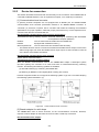
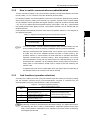
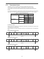
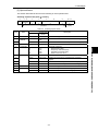
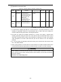
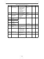
Listed below are documents relating to the FRENIC-Mini. Consult any appropriate document.
Name
Document number
Description
User's Manual
MEH446
Overview of FRENIC-Mini, how to operate the keypad, control
block diagram, selection of peripherals, capacity selection,
specifications, function codes, etc.
Catalog
MEH441
Overview of FRENIC-Mini, features, specifications, outline
drawing, options, etc.
Instruction Manual
INR-SI47-0791-E
Inspection at the time of product arrival, installation and
wiring, how to operate the keypad, troubleshooting,
maintenance and inspection, specifications, etc.
Installation Manual
INR-SI47-0773
Inspection at the time of arrival, how to install the product
These documents are subject to revision as appropriate. Obtain the latest versions when using the
product.
i
Safety Precautions
Prior to installation, connection (wiring), operation, maintenance or inspection, read through this user's
manual as well as the instruction and installation manuals to ensure proper operation of the product.
Familiarize yourself with all information required for proper use, including knowledge relating to the
product, safety information, and precautions.
This user's manual classifies safety precautions as shown below according to the severity of the
accident that may occur if you fail to observe the precaution:
Failure to heed the information indicated by this symbol may lead to dangerous
conditions, possibly resulting in death or serious bodily injuries.
Failure to heed the information indicated by this symbol may lead to dangerous
conditions, possibly resulting in minor or light bodily injuries and/or substantial
property damage.
Failure to heed the information contained under the CAUTION title can also result in serious
consequences. These safety precautions are of utmost importance and must be observed at all times.
The FRENIC-Mini is not designed for use in appliances and machinery on which lives depend. Consult
Fuji before considering the FRENIC-Mini series of inverters for equipment and machinery related to
nuclear power control, aerospace uses, medical uses or transportation. When the product is to be used
with any machinery or equipment on which lives depend or with machinery or equipment which could
cause serious loss or damage should this product malfunction or fail, ensure that appropriate safety
devices and/or equipment are installed.
Wiring
-
Before starting wiring, confirm that the power is turned OFF (open).
An electric shock may result.
-
The product cannot be connected directly to an RS232C interface.
Before connecting wiring to the connector (RJ45 connector) of an RS485 communications card,
confirm the wiring of the device to be connected. For further information, see "2.2 Connections"
under Chapter 2 of this manual.
Failure may result.
Operation
-
Note that the inverter starts to supply power to the motor and the motor runs upon resetting of an
alarm with the operation command ON (closed).
An accident may result.
ii
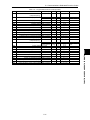
Table of Contents
1.1
Features.................................................................................................................................1-1
1.2
List of Functions.....................................................................................................................1-2
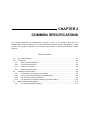
CHAPTER 2 COMMON SPECIFICATIONS
2.1
List of Specifications ..............................................................................................................2-1
2.2
Connections...........................................................................................................................2-2
2.2.1
Basic connection diagrams ............................................................................................2-2
2.2.2
Connection procedures ..................................................................................................2-3
2.2.3
Device for connection.....................................................................................................2-5
2.2.4
Measures against noise .................................................................................................2-6
2.3
Switching Communications ...................................................................................................2-8
2.3.1
Commands for switching communications.....................................................................2-8
2.3.2
How to switch communications enabled/disabled .........................................................2-9
2.3.3
Link functions (operation selection) ...............................................................................2-9
2.3.4
Link functions for supporting data input (operation select) ..........................................2-10
2.4
Making RS485-related Settings........................................................................................... 2-11
2.4.1
Link function (RS485 setting)....................................................................................... 2-11
CHAPTER 3 Modbus RTU PROTOCOL
3.1
Messages ..............................................................................................................................3-1
3.1.1
Message formats............................................................................................................3-1
3.1.2
Message types ...............................................................................................................3-1
3.1.3
Message frames.............................................................................................................3-2
3.1.4
Message categories .......................................................................................................3-3
3.1.5
Communications examples ............................................................................................3-7
3.2
Host Side Procedures............................................................................................................3-8
3.2.1
Inverter's response time.................................................................................................3-8
3.2.2
Timeout processing ........................................................................................................3-8
3.2.3
Receiving preparation complete time and message timing from the host .....................3-9
3.2.4
Frame synchronization method......................................................................................3-9
3.3
Communications Errors ....................................................................................................... 3-11
3.3.1
Categories of communications errors .......................................................................... 3-11
3.3.2
Operations in case of errors.........................................................................................3-12
3.4
CRC-16 ................................................................................................................................3-15
3.4.1
Overview of the CRC-16 ..............................................................................................3-15
3.4.2
Algorithm ......................................................................................................................3-15
3.4.3
Calculation example.....................................................................................................3-17
3.4.4
Frame length calculation ..............................................................................................3-18
CHAPTER 4 FUJI GENERAL-PURPOSE INVERTER PROTOCOL
4.1
Messages ..............................................................................................................................4-1
4.1.1
Message formats............................................................................................................4-1
4.1.2
Transmission frames......................................................................................................4-2
4.1.3
Descriptions of fields ....................................................................................................4-10
4.1.4
Communications examples .......................................................................................... 4-11
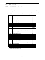
iii
CHAP.
4 CHAP.
3 CHAP. 2 CHAP. 1
TABLE
OF CONTENTS
CHAPTER 1 OVERVIEW
4.2
Host Side Procedures..........................................................................................................4-13
4.2.1
Inverter's response time...............................................................................................4-13
4.2.2
Timeout processing ......................................................................................................4-14
4.2.3
Receiving preparation complete time and message timing from the host ...................4-14
4.3
Communications Errors .......................................................................................................4-15
4.3.1
Categories of communications errors ..........................................................................4-15
4.3.2
Operations in case of communications errors .............................................................4-16
CHAPTER 5 FUNCTION CODES AND DATA FORMATS
5.1
Communications Dedicated Function Codes ........................................................................5-1
5.1.1
About communications dedicated function codes..........................................................5-1
5.1.2
Command data...............................................................................................................5-1
5.1.3
Monitor data ...................................................................................................................5-5
5.1.4
Information displayed on the keypad .............................................................................5-9
5.2
Data Formats .......................................................................................................................5-12
5.2.1
List of data format numbers .........................................................................................5-12
5.2.2
Data format specifications............................................................................................5-21
iv
CHAPTER 1
OVERVIEW
This chapter describes the functions that can be realized by performing RS485 communications on the
FRENIC-Mini.
Table of Contents
1.1
Features.................................................................................................................................1-1
1.2
List of Functions.....................................................................................................................1-2
1.1 Features
1.1
Features
The functions listed below become available by installing an RS485 communications card
(option) in the FRENIC-Mini:
A remote keypad can be mounted on an easy-to-access front of control panel by connecting
the remote keypad to the RS485 communications card through an extension cable (option;
minimum wiring length: 20m).
- The function code data of the inverter can be edited and the operation status of the inverter
can be monitored by connecting it to a personal computer on which inverter support software
runs (see the "Inverter Support Software FRENIC Loader Instruction Manual").
- The inverter can be managed and controlled as a subordinate unit (slave) by connecting it to
a host controller (master), such as a PLC and a personal computer.
As the communication protocols for controlling inverter, the Modbus RTU widely used by a
variety of appliances, and the Fuji general-purpose inverter protocol common to Fuji's inverters
including conventional models, are available.
Modbus RTU protocol
The Modbus RTU protocol is a set of communications specifications defined to connect
Modicon's PLCs in a network. A network is established between PLCs or between a PLC and
another slave unit(s) (inverter(s), etc.). The main functions include:
-
supporting both a query-response format and a broadcast format for messages;
enabling the host computer as the master to transmit queries to each inverter as a slave, and
each slave to send back responses to the queries to the master;
- supporting RTU and ASCII modes as transmission modes in the standard Modbus protocol,
whereas the FRENIC-Mini supports only RTU mode that provides a high transmission
density; and
- performing an error check through a CRT (cyclic redundancy check) to ensure accurate data
transmission.
Fuji general-purpose inverter protocol
This protocol is commonly used for all models of Fuji's general-purpose inverters. The main
functions include:
-
enabling, as a common protocol, operation of all models of Fuji's general-purpose inverters
with the same host program (function codes cannot be generally edited because
specifications are different among models);
-
adopting a fixed-length transmission frame (standard frame) to facilitate program
development for the host; and
-
reducing the communications time in response to operation commands and frequency
setting requiring quick response by using an optional transmission frame.
-
The remote keypad uses a dedicated protocol. By connecting the remote keypad,
the protocol automatically switches to the dedicated protocol; thereby the setting of
communications-related functions is not required.
-
Although the personal computer loader uses a dedicated protocol for loader
commands, part of the communications conditions must be set. (For further
information, see the "Inverter Support Software FRENIC Loader Instruction
Manual.")
-
With regard to a FRENIC-Mini that uses inverter ROM 0399 or earlier version, part
of the RTU protocol functions are restricted. Contact us for these restrictions.
Confirm the ROM version according to the menu "5_14" described in "3.8 Reading
Maintenance Information" under Chapter 3 of the FRENIC-Mini Instruction Manual.
1-1
OVERVIEW CHAP. 1
-
1.2
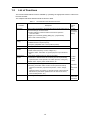
List of Functions
The functions listed below become available by operating the appropriate function codes from
the host controller.
The chapters that follow describe these functions in detail.
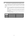
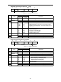
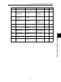
Table 1.1
List of RS485 communications functions
Function
Operation
Description
The functions equivalent to the terminal functions shown below can be
executed through communications:
-Forward operation command "FWD" and reverse operation
command "REV"
Related
function
code
S codes
(dedicated
to communications)
-Digital input commands ([FWD], [REV], [X1] - [X3] terminals)
-Alarm reset command ("RST")
Frequency
setting
Either of the following two setting methods can be selected:
-±20000/maximum output frequency
-Frequency (adjustable unit: 0.01 Hz) without polarity
PID command
-Setting within ±20000/100%
Operation
monitor
-Frequency command
M codes
-Actual values (frequency, current, voltage, etc.)
-Operation status, information on general-purpose output terminals,
etc.
Maintenance
monitor
-Cumulative operation time, DC link-circuit voltage
-Information to determine the service life of parts to be periodically
replaced (main circuit capacitor, PC board capacitor, cooling fan)
-Model codes, capacity codes, ROM version, etc.
Alarm monitor
-Monitoring alarm history (last three alarms)
-Monitoring information when an alarm occurs (last three alarms)
Operation information (output/set frequencies, current, voltage,
etc.)
Operation status, information on general-purpose output terminals
Maintenance (cumulative operation time, DC link-circuit current,
heat sink temperature, etc.)
Function code
Monitoring and changing function code data
1-2
W codes
X codes
Z codes
(dedicated
to
communications)
All function
codes other
than above
CHAPTER 2
COMMON SPECIFICATIONS
This chapter describes the specifications common to both of the Modbus RTU and Fuji
general-purpose inverter protocols. For further information about the specific specifications of each
protocol, see Chapter 3 "Modbus RTU Protocol" and Chapter 4 "Fuji General-purpose Inverter
Protocol."
Table of Contents
2.1
List of Specifications ..............................................................................................................2-1
2.2
Connections...........................................................................................................................2-2
2.2.1
Basic connection diagrams ............................................................................................2-2
2.2.2
Connection procedures ..................................................................................................2-3
2.2.3
Device for connection.....................................................................................................2-5
2.2.4
Measures against noise .................................................................................................2-6
2.3
Switching Communications ...................................................................................................2-8
2.3.1
Commands for switching communications.....................................................................2-8
2.3.2
How to switch communications enabled/disabled .........................................................2-9
2.3.3
Link functions (operation selection) ...............................................................................2-9
2.3.4
Link functions for supporting data input (operation select) ..........................................2-10
2.4
Making RS485-related Settings........................................................................................... 2-11
2.4.1
Link functions (RS485 settings) ................................................................................... 2-11
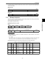
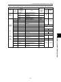
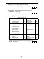
2.1 List of Specifications
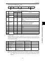
List of Specifications
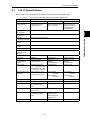
Shown below are the specifications for RS485 communications of the FRENIC-Mini:
Table 2.1
List of RS485 communications specifications of the FRENIC-Mini
Item
Specification
Protocol
FGI-BUS
Modbus RTU
Loader commands
Complying with
Fuji general-purpose
inverter protocol
Modicon's Modbus RTU
(RTU mode only)
Special commands
dedicated to inverter
support software
(not disclosed)
Number of units to
be connected
1 host and 31 inverters
Electrical
specification
EIA RS485
Method of
connection to RS485
Using 8-pin RJ45 connectors
Synchronization
system
Start-stop synchronization
Communication
system
Half-duplex system
Baud rate (bps)
2400, 4800, 9600, and 19200
Maximum
communications
distance
500m
Number of stations
1 to 31
1 to 247
1 to 255
Frame type
FGI-BUS
Modbus RTU
Loader command
Frame
synchronization
system
Header character
detection (SOH)
Data absence time
detection
(for three bytes)
Header character
detection
(start code 96H)
Frame length
General transmission:
16 bytes, fixed
Variable length
Variable length
During writing:
50 words
During writing:
41 words
During reading:
50 words
During reading:
41 words
High-speed transmission:
8 bytes or 12 bytes
Maximum data to be
transferred
During writing: 1 word
During reading: 1 word
Message system
Polling, selecting, and broadcast
Command message
Character system
ASCII
Binary
Binary
Character length
8 bits or 7 bits selectable
according to function
code
8 bits, fixed
8 bits, fixed
Parity
Even, odd or without parity selectable according to
function code
Even parity
Stop bit length
1 bit or 2 bits selectable
according to function
code
When "without parity"
selected: 2 bits
1 bit, fixed
Check sum
CRC-16
Error check system
2-1
When "with parity"
selected: 1 bit
Check sum
COMMON SPECIFICATIONS CHAP. 2
2.1
2.2
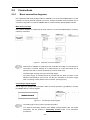
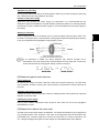
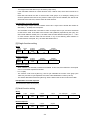
Connections
2.2.1
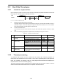
Basic connection diagrams
Use a standard LAN cable (straight cable for 10BASE-T) to connect the FRENIC-Mini to a host
controller, such as a personal computer and a PLC, through an RS485 communications card. A
converter is required to connect the FRENIC-Mini to a host controller without RS485 interface.
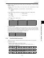
Multi-drop connection
Use a branch adapter for multi-drops as shown below to connect the FRENIC-Mini to a host by
multi-drop connection.
Figure 2.1
Multi-drop connection diagram
-
Select branch adapters for multi-drops and converters according to "2.2.3 Device for
connection" to prevent damage to or malfunctioning of control PC boards due to
external noise and to remove the effects of common mode noise.
-
The total length of wiring must not exceed 500 meters.
-
The power supply for remote keypad is provided with the RJ45 connector of the
RS485 communications card. Do not use the pins assigned to the power supply
when connecting another device to this connector. (See Figure 2.3.)
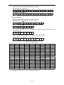
Connecting a remote keypad
Use an eight-core straight cable (extension cable for remote operation, type CB-5S) to connect
the FRENIC-Mini to a remote keypad.
Figure 2.2
Connecting a remote keypad
・ The total length of wiring must not exceed 20 meters.
・ Turn OFF the terminating resistor of the RS485 communications card. For further
information, see the section of Terminating resistor under "2.2.2 Connection
procedures."
2-2
2.2 Connections
2.2.2
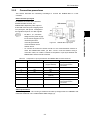
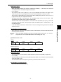
Connection procedures
This section describes the necessary knowledge to connect the FRENIC-Mini to a host
controller.
To facilitate connection with a standard
RS232C-RS485 converter, the
FRENIC-Mini adopts two pairs of pins of
RJ45 LAN connector pins complying with a
four-pair layout, with pin No. 4 assigned to
DX- signals and pin No. 5 to DX+ signals.
-
-
Pin Nos. 1, 2, 7, and 8 are
assigned to the power supply
for the remote keypad. Do not
use these pins when
Figure 2.3 FRENIC-Mini's pin layout
connecting this RS485
communications card to
another device.
To connect the FVR-E11S series inverter on the communications network on
which the FRENIC-Mini exists, pin Nos. 3 and 5 must be switched using a
connection cable, etc. Table 2.2 makes a comparison of pin layout between the
FRENIC-Mini and the FVR-E11S series.
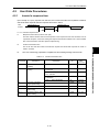
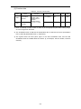
Table 2.2
Comparison of pin layout between the FRENIC-Mini and the FVR-E11S
Pin No.
FRENIC-Mini
FVR-E11S
1
VCC (+5V)
SEL_TP
(keypad selected)
2
GND
GND
3
NC
DX+
4
DX-
DX-
5
DX+
SEL_ANY
(optional)
6
NC
GND
7
GND
VCC
8
VCC (+5V)
VCC
Remarks
The power supply is
short-circuited when
connected.
The power supply is
short-circuited when
connected.
Cable specifications
Connect only pin Nos. 4 and 5 using a standard LAN cable (a straight cable for 10BASE-T that
meets the standards of U.S. ANSI/TIA/EIA-568A Category 5).
2-3
COMMON SPECIFICATIONS CHAP. 2
RJ45 connector pin layout
Terminating resistor
Insert a terminating resistor (100 to 120Ω) into both
ends of the wiring, which can suppress the
reflection of signals and reduce noise. This RS485
communications card contains a 120Ω terminating
resistor that can be inserted and open with the
SW1.
Terminating resistors can be inserted by turning ON
the SW1 shown in Figure 2.4.
Figure 2.4 SW1 of the RS485
communications card
Insert a terminating resistor into the terminal master unit and the slave unit (inverter)
connected to the last end, or both terminal units comprising the network. This
means that a terminating resistor is inserted into a total of two units. Note that
inserting a terminating resistor into three or more units may cause a shortage of
signal current capacity.
Connecting a four-wire RJ45 to a host controller
Although the FRENIC-Mini uses two-wire cables, some hosts adopt four-wire cables. The
FRENIC-Mini can be connected to such a host with a two-wire cable by connecting the driver
outputs and receiver inputs of the host with a crossover cable.
Figure 2.5
Connecting the FRENIC-Mini to a four-wire type host
-
The host must have the function to set the driver outputs to high impedance
(driver enable). Confirm that products conforming to RS485 are provided with this
function.
-
Keep the driver outputs in the status of high impedance except when the host is
transmitting data (driver enable: OFF).
-
Keep the receiver in the host deactivated (receiver enable: OFF) during
transmission to prevent the host from receiving the data it has transmitted. If the
receiver cannot be deactivated, program the host so that it will discard the data it
transmits.
2-4
2.2 Connections
2.2.3
Device for connection
This section describes the devices that are necessary for the connection of the FRENIC-Mini to
a host without RS485 interface, such as a personal computer, or for multi-drop connections.
In general, personal computers are not equipped with an RS485 port. An RS232C-RS485
communications level converter (hereinafter referred to as "RS232C-RS485 converter" or
"converter") is, therefore, required. Use a converter that meets the following recommended
specifications for proper operation. Note that proper performance may not be expected from a
converter other than the recommended one.
Recommended communications level converter specifications
Transmission/receiving switching system: Automatic switching by monitoring data transmitted
on the personal computer (RS232C)
Isolation:
The converter must be isolated from the RS485 side.
Failsafe:
Equipped with a failsafe function (*)
Other requirements:
The converter must have excellent noise immunity.
* The failsafe function means a function that enables the RS485 receiver output to ensure the
status of logic high even when the RS485 receiver input is open or short-circuited or when all
of the drivers of the RS485 are inactive.
Recommended communications level converter
System Sacom-made KS-485PTI
Transmission/receiving switching system
Since the RS485 communications card for the FRENIC-Mini adopts a half-duplex system
(two-wire system), the converter to be used must have a transmission/receiving switching
function. The following two switching systems are available:
(1) Automatic switching by monitoring transmitted data
(2) Switching by RS232C control signals (RTS or DTR), (flow control)
Personal computer loaders do not support the switching system of (2). Use a converter adopting
the switching system described in (1).
Figure 2.6
Communications level conversion
[2] Branch adapter for multi-drops
The FRENIC-Mini uses an RJ45 connector for the communications connector, therefore,
requires a branch adapter for the RJ45 connector to make a multi-drop connection.
Recommended branch adapter
SK Kohki-made MS8-BA-JJJ
2-5
COMMON SPECIFICATIONS CHAP. 2
[1] Communications level converter
2.2.4
Measures against noise
Depending on the operating environment, the FRENIC-Mini may not ensure normal
communications due to noise generated by the inverter, or any of the instruments and converter
of the master may malfunction. This section describes measures to be taken against such
problems. Consult Appendix A "Advantageous Use of Inverters (Notes on electrical noise)" to
the FRENIC-Mini User's Manual as well.
[1] Measures for devices subjected to noise
Isolated converter
Eliminate common mode noise that exceeds the specified operating voltage range of the
receiver in case of long-distance wiring. However, since the isolated converter itself may
malfunction, use a converter insusceptible to noise.
Category 5 compliant LAN cable
Category 5 compliant LAN cables are generally used for RJ45 connector wiring. To obtain an
improved preventive effect on electromagnetically induced noise, use Category 5 conformed
four-pair twisted pair LAN cables, DX+ and DX- in pairs (twisted pairs). To ensure a high
preventive effect on electrostatically induced noise, use Category 5 conformed four-pair
shielded twisted pair LAN cables, with the master-side end of the shield grounded.
Effect of twisted pair cables
A uniform magnetic flux directing from the face to back of the paper exists, and if it varies (increases),
electromotive force in the direction of → is generated. The electromotive forces of A to D are the same
in intensity and flow in the directions shown in the above figure. In the cable DX+ in this case,
electromotive forces B and C flow in the opposite directions and offset each other, and so do
electromotive forces A and D in the cable DX-. So, normal mode noise caused by electromagnetic
induction does not occur. However, noise cannot be completely suppressed under such conditions as
an uneven twist pitch. Thus, noise is eliminated in twisted cables but normal mode noise occurs in
parallel cable.
Shield effect
1) When the shield is not grounded,
the shield functions as an antenna and receives noise.
2) When the shield is grounded at both ends,
if the grounding points are separated from each other, the ground potential may be different between
them, and the shield and the ground form a loop circuit in which a current flows and may cause noise.
Additionally, the magnetic flux within the loop may vary and generate noise.
3) When the shield is grounded at either end,
the effect of electrostatic induction can be completely eliminated within the shielded section.
Terminating resistor
Insert a resistor equivalent to the characteristic impedance of the cables (100 to 120Ω) into both
end terminals of the wiring (network) to prevent ringing due to the reflection of signals.
Separation of the wiring
Separate the power lines (input R, S, and T and output U, V, and W) and the RS485
communications line from one another because induced noise can be prevented.
2-6
2.2 Connections
Separation of grounding
Do not ground instruments and the inverter together. Noise may conduct through the grounding
wire. Use as a thick wire as possible for grounding.
Isolation of the power supply
Noise may carry through the power supply for instruments. It is recommended that the
distribution system be separated or a power isolation transformer (TRAFY) or noise suppression
transformer be used to isolate the power supply for such instruments from the power supply for
the inverter.
Insert a chalk coil in series in the signal circuit, or pass the signal wiring through a ferrite core,
as shown in the figure below. This provides the wiring higher impedance against high-frequency
noise, and suppresses the propagation of high-frequency noise.
If an inductance is added, the signal waveform may become irregular and a
transmission error may result during communications at a high baud rate. In this case,
reduce the baud rate by changing the setting of function code y04.
[2] Measures against noise sources
Carrier frequency
By reducing the setting of function code F26 "motor sound (carrier frequency)," the noise level
can be reduced. However, reducing the carrier frequency increases the running noise level of
the motor.
Installing and wiring an inverter
Passing the power lines through metal conduit or adopting metal control panels can suppress
radiation or induction noise.
Isolating the power supply
Using a power isolation transformer as the power for the inverter can cut off the propagation
(transmission) of noise.
[3] Measures to reduce the noise level
Consider using a zero-phase reactor or EMC filter. The measures described in [1] and [2] above
can generally prevent noise. However, if the noise of the equipment does not decrease to the
permissible level, consider measures to reduce the noise level. For further information, see
"6.4.1 Peripheral Equipment Options" under Chapter 6 of the FRENIC-Mini User's Manual.
2-7
COMMON SPECIFICATIONS CHAP. 2
Adding an inductance
2.3
Switching Communications
2.3.1
Commands for switching communications
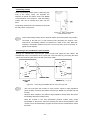
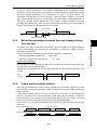
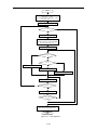
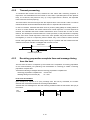
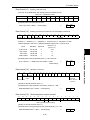
Figure 2.7 below shows a block diagram via communications, including the systems for
frequency setting and operation commands.
This block diagram is part of the switching section, and there are configuration settings that are
given priority over the blocks illustrated here. For further information about blocks, including
peripheral devices, see “Chapter 4 BLOCK DIAGRAM FOR CONTROL LOGIC” of the
FRENIC-Mini User's Manual.
Operation commands herein include via-communications digital input signals.
According to the setting of function code H30 link function (operation selection), the command
system when communications is valid is selected.
Even if digital input is set to link operation, while making the link invalid ("LE" = OFF), the
command system switches from communications to other settings including digital input signal.
The frequency setting, the forward operation command, and the X1 signal shown in Figure 2.7
switch from S01, S05, and S06 to [12], [FWD], and [X1], respectively.
Communications/Terminal
block switching
OFF
Set
frequency
【12】
Frequency
setting
Link function Link function
for aid
H30
Host
Communications
Set frequency for
communications
S01
【FWD】
ON
y99
0,2
1,3
S01≠0
1,3
S01=0
S05
Forward operation
command
0,2
Set frequency for
communications
OFF
Operation command
0,1
S06
bit 0
Terminal FWD
(function selection)
Operation command
2,3
Turned
ON at
98
bit 13
Terminal REV
(function selection)
Operation command
ON
y99
0,1
2,3
E98
S06
Forward operatio
command
Link function Link function
for aid
H30
E99
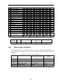
Table of truth values of S06 (bit 13,
bit 14) computing unit
S06
bit 14
S06 (bit 13, bit 14)
computing unit
Turned
ON at
98
bit 13
bit 14
ON
ON
Output
ON
ON
OFF
OFF
OFF
ON
OFF
OFF
OFF
OFF
ON
-
ON
OFF
-
OFF
-
ON
ON
-
OFF
OFF
-: Not assigned
(The value of the assigned bit will be output.)
Digital input
OFF
【X1】
Link function Link function
for aid
H30
0,1
y99
0,1
2,3
Operation command 1
2,3
S06
bit 2
Digital input (link
operation selection)
Depends on the set function.
『LE』
Figure 2.7
Operation command block diagram via communications
2-8
ON
X1 signal
2.3 Switching Communications
2.3.2
How to switch communications enabled/disabled
To issue a frequency setting or via-communications operation command and thereby control the
inverter, select 1, 2 or 3 of function code H30: Serial link (function select).
Communications automatically becomes valid when link operation selection is not assigned to
any digital input terminal.
Table 2.3
Digital input terminal settings and communications statuses
Input terminal
Status
OFF
Communications invalid
ON (short-circuited to
the terminal [CM])
2.3.3
Communications valid
-
Via-communications command data and operation data must be rewritten from the
host (controller) because the memory is initialized when the power is turned ON.
-
Although command data and operation data can be written even if communications
is invalid, they will not be validated because the switch is made invalid by link
operation selection. If communications is made valid with no operation data written
(operation command OFF, frequency setting = 0Hz) during operation, the running
motor decelerates to a stop and may exert impact on the load depending on the set
deceleration time. Operation can be switched without causing impact to the load by
setting data in communications invalid mode in advance and then switching the
mode to valid.
-
If negative logic is set as Link enable (data 1024), the logical value corresponding to
the ON/OFF status of the command "LE" will be reversed.
Link functions (operation selection)
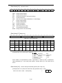
According to the setting of function code H30: Serial link (function select), the frequency setting
and the operation command source (via-communications command or command from the
external signal input) when communications is valid can be selected.
Table 2.4
Link function
H30
Link function (operation selection)
When communications is valid
Frequency setting
Operation command
0
External signal input valid
(frequency setting 1, 2)
1
Communications valid (S01, S05)
2
External signal input valid
(frequency setting 1, 2)
3
Communications valid (S01, S05)
External signal input valid
(Operation command by F02)
(Terminal block digital input valid)
Communications valid (S06)
By selecting continuous communications valid without setting any digital input terminal,
and switching the data of H30 to communications valid/invalid (external signal input
valid), communications valid/invalid can be switched in the same manner as switching
at the digital input terminal.
2-9
COMMON SPECIFICATIONS CHAP. 2
For switching between via-communications control and control from the terminal block (external
signal input) (frequency setting from terminal [12], operation command from terminal [FWD],
etc.) and between remote operation and keypad operation, assign link operation selection (data
= 24: “LE”) to any digital input terminal-related function code of (E01 – E03: [X1] – [X3] terminals,
E98: [FWD] terminal, E99: [REV] terminal). Link operation selection can be switched with the
assigned terminal.
2.3.4
Link functions for supporting data input (operation select)
According to the setting of function code y99: link function for supporting data input (operation
select), the frequency setting and the operation command source (via-communications
command or command specified by H30) when communications is valid can be selected
individually.
-
This function code is designed for inverter support software for personal computer
loaders such as FRENIC Loader, and forcibly makes communications valid without
changing the setting of H30. Do not change the current setting unless otherwise
required.
- This function code, if changed from the inverter, provides the function equivalent to
y99 = 0. The data of y99 must be written from communications when setting it to a
value other than 0.
- The data of this function code cannot be saved in the inverter and will return to 0
when the power is turned OFF.
Table 2.5
Link function
y99
Link functions for supporting data input
When communications is valid
Frequency setting
Operation command
0
Frequency setting specified by H30
Operation command specified by H30
1
Communications valid (S01, S05)
2
Frequency setting specified by H30
3
Communications valid (S01, S05)
2-10
Communications valid (S06)
2.4 Making RS485-related Settings
2.4
Making RS485-related Settings
2.4.1
Link function (RS485 setting)
Use function codes (y01 – y10) to make settings for RS485 communications functions.
Station address (y01)
Set a station address for RS485 communications. The setting range depends on the protocol.
y01: RS485 setting (station addresses)
Range
Broadcast
Modbus RTU protocol
Protocol
1 to 247
0
Protocol for loader commands
1 to 255
-
Fuji general-purpose inverter protocol
1 to 31
99
-
Response does not occur if a value out of the specified range is set.
-
Match the station address with that of the personal computer when a personal
computer loader is connected.
Mode selection on no response error (y02)
Set the action to be performed when an RS485 communications error occurs.
Table 2.7
y02: RS485 setting (in case of error)
Data
Function
0
When RS485 communications error occurs, the ongoing operation is immediately
interrupted by the alarm "Er8".
1
When RS485 communications error occurs, the ongoing operation is interrupted by
the alarm "Er8" after operation is performed for the period of time set by the timer.
2
When RS485 communications error occurs, the ongoing operation is interrupted by
the alarm "Er8" if communications are retried during operation for the period of time
set by the timer but is not recovered.
3
The ongoing operation continues even if a communications error occurs.
If the personal computer goes out of control when a personal computer loader is
connected and its trial operation function is used, a stop command may not be issued.
In this case, it may be impossible to deactivate the inverter. To ensure safety, select the
appropriate setting in case of occurrence of communications error.
Timer (y03)
Set an error processing time.
-
Data setting range: 0.0 to 60.0 (seconds)
Table 2.8
Baud rate (y04)
Data
Set a baud rate.
- Setting when a personal computer loader is
connected
Match the baud rate with that of the personal
computer.
2-11
Baud rate
Baud rate
0
2400 bps
1
4800 bps
2
9600 bps
3
19200 bps
COMMON SPECIFICATIONS CHAP. 2
Table 2.6
Table 2.9
Data length (y05)
Data length
Data
Set a character length.
- Setting when FRENIC Loader is connected
This code does not need to be set because it is
automatically set to eight bits (as in the Modbus
RTU protocol).
Function
0
8 bits
1
7 bits
Table 2.10
Parity check (y06)
Parity check
Data
Set a parity bit.
- Setting when FRENIC Loader is connected
This code does not need to be set because it is
automatically set to even parity.
Function
0
No parity bit
1
Even parity
2
Odd parity
Table 2.11
Stop bits (y07)
Data
Set a stop bit.
- Setting when FRENIC Loader is connected
This code does not need to be set because it is
automatically set to 1.
Stop bits
Function
0
2 bits
1
1 bit
- In the Modbus RTU protocol, this code does not
need to be set because it is automatically
determined in conjunction with the parity bit.
Table 2.12 No response error
detection time
No response error detection time (y08)
In a system designed to access a station
(inverter) regularly controlled by the host within a
specific period of time, access may be lost during
RS485 communications due to wire
disconnection. Set the period of the time when the
inverter detects it until when the ongoing
operation is interrupted by an alarm with RS485
communications error "Er8."
-
Data
0
1 to 60
Function
No response error
detection disabled
Detecting time from 1
to 60 seconds
Setting when FRENIC Loader is connected
Communications from FRENIC Loader to the inverter takes place at fixed intervals or only
when an event occurs as a result of operation, depending on the functions selected. For this
reason, select the setting of disabling communications interruption detection (data = 0).
(For example, although communications is performed at a fixed cycle of approximately
800ms during trial operation, the cycle varies according to the processing by the operating
system of the personal computer.)
2-12
2.4 Making RS485-related Settings
Response interval (y09)
Set the time from the completion of receipt of a request from the personal computer or PLC, to
the return of response to it. Even in a slow processing device, timing can be adjusted by
changing the response interval time.
-
Data setting range: 0.00 to 1.00 (second)
Master
Request
Inverter
Response
t1 = Response interval time + α
α:
-
The processing time within the inverter. It depends on the timing and command given.
For further information, see the procedure for each protocol on the host below:
Modbus RTU protocol → Chapter 3 "3.2 Host Side Procedures"
Fuji general-purpose inverter protocol → Chapter "4.2 Host Side Procedures"
Setting when FRENIC Loader is connected
Set the response interval time according to the performance and conditions of the personal
computer and converter (RS485/RS232C converter, etc.).
(Some converters monitor the communications status and use a timer to switch
transmission/receiving.)
Table 2.13
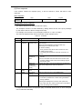
Protocol select (y10)
Data
Select a communications protocol.
-
Setting when FRENIC Loader is
connected
Select the protocol for FRENIC Loader
commands (y10 = 1).
2-13
Protocol select
Protocol
0
Modbus RTU
1
FRENIC Loader
2
Fuji general-purpose inverter
COMMON SPECIFICATIONS CHAP. 2
t1
2-14
CHAPTER 3
Modbus RTU PROTOCOL
This chapter describes the Modbus RTU protocol, as well as the host side procedure for using this
protocol and error processing.
The Modbus RTU protocol was a set of specifications developed in the United States. For the
FRENIC-Mini of which inverter ROM version is 0399 or earlier, the Modbus RTU functions are partially
restricted. Contact us about details of restrictions. Check the inverter ROM version with menu "5_14"
described in "3.8 Reading Maintenance Information" under Chapter 3 of the FRENIC-Mini Instruction
Manual.
Table of Contents
3.1
Messages ..............................................................................................................................3-1
3.1.1
Message formats............................................................................................................3-1
3.1.2
Message types ...............................................................................................................3-1
3.1.3
Message frames.............................................................................................................3-2
3.1.4
Message categories .......................................................................................................3-3
3.1.5
Communications examples ............................................................................................3-7
3.2
Host Side Procedures............................................................................................................3-8
3.2.1
Inverter's response time.................................................................................................3-8
3.2.2
Timeout processing ........................................................................................................3-8
3.2.3
Receiving preparation complete time and message timing from the host .....................3-9
3.2.4
Frame synchronization method......................................................................................3-9
3.3
Communications Errors ....................................................................................................... 3-11
3.3.1
Categories of communications errors .......................................................................... 3-11
3.3.2
Operations in case of errors.........................................................................................3-12
3.4
CRC-16 ................................................................................................................................3-15
3.4.1
Overview of the CRC-16 ..............................................................................................3-15
3.4.2
Algorithm ......................................................................................................................3-15
3.4.3
Calculation example.....................................................................................................3-17
3.4.4
Frame length calculation ..............................................................................................3-18
Fuji Electric Co., Ltd.
ED&C • Drive Systems Company
Gate City Ohsaki, East Tower, 11-2, Osaki 1-chome
Shinagawa-ku, Tokyo 141-0032, Japan
Phone: +81-3-5435-7139 Fax: +81-3-5435-7458
Printed on 100% recycled paper
Information in this manual is subject to change without notice.
Printed in Japan 2002-10 (J02/J02) CM 10 FIS
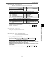
3.1 Messages
3.1
Messages
3.1.1
Message formats
The regular formats for transmitting RTU messages are shown below:
Inverter's response time
(Slave Turn-around Time)
Broad cast transaction
Host
(master)
Inverter
(slave)
Host
(master)
Inverter
(slave)
Query message
Response
Broadcast message
No response
If the inverter receives from the host a message in the standby status and considers it properly
received, it executes a transaction in response to the request and sends back normal response.
If the inverter judges that the message has not been received properly, it returns error response.
The inverter does not send back any response in the case of broadcast transactions.
3.1.2
Message types
Message types are classified into four types; query, normal response, error response, and
broadcast.
Query
The host sends messages to a single inverter.
Normal response
After the inverter received a query from the host, the inverter executes a transaction in response
to the request, and sends back corresponding normal response.
Error response
If the inverter receives a query but cannot execute the requested function because an invalid
function code is specified or for other reasons, it sends back error response.
The error response is accompanied by a message describing the reason the request cannot be
executed.
The inverter cannot send back any response in case of a CRC or physical transmission error
(parity error, framing error, overrun error).
Broadcast
The master uses address 0 to send messages to all slaves. All slaves, which receive a
broadcast message, execute the requested function. This transaction will be terminated upon
timeout of the master.
3-1
Modbus RTU PROTOCOL CHAP. 3
Query transaction
3.1.3
Message frames
As shown below, a transmission frame consists of four blocks, which are called fields. Details
depend on RTU function codes. To make a clear distinction between RTU function codes and
the inverter's function codes, the former will be hereinafter referred to as FCs.
1 byte
Station address
1 byte
FC (RTU function code)
Up to 105 bytes
Information
2 bytes
Error check
Station address
The station address field is one byte long, in which a station address between 0 and 247 can be
selected.
Selecting address 0 means the selection of all slave stations and a broadcast message.
FC (RTU function code)
The FC field is one byte long, in which a function code is defined with a number from 0 to 255.
The FCs in hatching are available. Do not use any unavailable FC. Failure to observe this rule
results in error response.
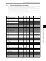
Table 3-1
List of FCs
FC
Description
0 to 2
Unused
3
Function reading (up to 50)
4 to 5
Unused
6
Single function writing
7
Unused
8
Maintenance code
9 to 15
Unused
16
Serial function writing (up to 50 data)
17 to 127
Unused
128 to 255
Reserved for exception response
Information
The information field contains all information (function code, byte count, number of data, data,
etc.). For further information about the information field for each message type (broadcast,
query, normal response, error response), see "3.1.4 Message categories."
Error check
The error check field is a CRC-16 check system and two bytes long. Since the length of the
information field is variable, the frame length required for calculating the CRC-16 code is
calculated based on the FC and the byte count data.
For further information about CRC-16 calculations and algorithm, see "3.4 CRC-16."
For byte counts, see "3.1.4 Message categories."
Character format
Each byte of a message is transmitted as a character. Character formats are described on the
following page.
A character comprises a start bit (logical value 0), 8-bit data, an additional (optional) parity bit,
and a stop bit (logical value 1).
3-2
3.1 Messages
A character always consists of eleven bits, and the number of stop bits varies depending on
whether parity exists.
Without parity
LSB
MSB
0
Start
1
2
3
4
5
6
7
8
Data
9
10
Stop
With parity
LSB
MSB
0
Start
2
3
4
5
6
7
8
9
Parity (optional)
10
Stop
Message categories
There are five RTU message categories; function reading, single function writing, serial function
writing, maintenance code, and error response.
Each category is described below:
[1] Reading function codes
Query
1 byte
Station
address
1 byte
03H
2 bytes
Function code
Hi
Lo
2 bytes
Number of data
read
Hi
Lo
2 bytes
Error check
Normal response
1 byte
Station
address
1 byte
03H
1 byte
Byte count
2 to 100 bytes
Number of data read
2 bytes
Error check
Hi, Lo (data 0); Hi, Lo (data 1); ·····
How to set a query
-
This request is not available for broadcast transactions. Station address 0 will become
invalid (no response).
-
FC = 3 (03H)
-
The function code is two bytes long. The Hi byte indicates the function code group (see
Table 3.2), and the Lo byte represents a function code identification number (0 to 99).
(Example) When the function code is E15, the Hi byte is 01H and the Lo byte is 0FH.
Table 3.2
Group
Code
Function code group/code conversion table
Name
Group
Code
Name
F
0
00H
Fundamental
function
M
8
08H
Monitor data
E
1
01H
Extension terminal
function
J
13
0DH
Application function
C
2
02H
Control function of
frequency
y
14
0EH
Link function
P
3
03H
Motor parameter
W
15
0FH
Monitor 2
H
4
04H
High performance
function
X
16
10H
Alarm 1
S
7
07H
Command/
Function data
Z
17
11H
Alarm 2
3-3
Modbus RTU PROTOCOL CHAP. 3
3.1.4
1
Data
-
The length of the read data is up to 50 words (2 byte each).
If the read data contains an unused function code, 0 will be read, which will not result in an
error.
Data does not extend over two or more function code groups. If, for example, reading of 40
words is specified from F40 but only function codes up to F40 are available, the data of F40
will be set at the first word, and the other 49 words will be 0.
Interpretation of normal response
-
The data range of byte counts is between 2 and 100. A byte count is double the number of
data read (1 - 50 data) of the response.
-
The read data contains each word data in order of Hi byte and Lo byte, and each word data
is sent back in order of the data of the function code (address) requested by the query, the
data of that address number plus 1, the data of that number address number plus 2 ... If two
or more function data are read and the second or any of the following data contains an
unused function code (F09, etc.), the read data will become 0.
[2] Single function writing
Query
1 byte
Station
address
1 byte
06H
2 bytes
Function
code
Hi
Lo
2 bytes
Data written
Hi
2 bytes
Error check
Lo
Normal response
1 byte
Station
address
1 byte
06H
2 bytes
Function
code
2 bytes
Data written
2 bytes
Error check
How to set a query
-
When address 0 is selected, broadcast is available. In this case, all inverters do not respond
even if a broadcast request is executed.
FC = 6 (06H)
The function code is two bytes long. The Hi byte indicates the function code group (see
Table 3.2), and the Lo byte represents a function code identification number (0 to 99).
The written data field is fixed two bytes long. Set the data on the function code to be written.
Interpretation of normal response
The frame is the same as the query.
[3] Serial function writing
Query
1 byte
Station
address
1 byte
10H
2 bytes
Function
code
Hi
Lo
2 bytes
Number of data
written
Hi
Lo
1 byte
Byte count
2 bytes
Function
code
2 bytes
Number of data
written
2 bytes
Error check
Hi, Lo; Hi, Lo…
Normal response
1 byte
Station
address
1 byte
10H
3-4
2 to 100 bytes
Data written
2 bytes
Error check
3.1 Messages
-
-
When the station address 0 is selected, broadcast is available. In this case, all inverters do
not respond even if a broadcast request is executed.
FC = 16 (10H)
The function code is two bytes long. The Hi byte indicates the function code group (see
Table 3.2), and the Lo byte represents a function code identification number (0 to 99).
The number of data written is two bytes long, and the setting range is from 1 to 50. If 51 or a
higher value is set, error response will result.
The byte count field is one byte long, and the setting range is from 2 to 100. Set a value
equivalent to the double of the number of data written.
Set the lowest order code (the data on the function code requested by the query) at the first
two bytes of the data written, and the higher order data (address plus 1, address plus 2 ...) at
the following bytes.
If the data written contains an unused function code, the writing will be ignored, which will not
result in an error.
Interpretation of normal response
-
With regard to the function code and the number of data written, the same values as those of
the query will be sent back.
- When H03 (Data initialization) is used, use single function writing (FC = 6). H03 will
be ignored even if it is written with serial function writing (FC = 16).
[4] Maintenance code
Query
1 byte
Station
address
1 byte
08H
2 bytes
Diagnosis code
0000H
2 bytes
Data written
Hi
2 bytes
Error check
Lo
Normal response
1 byte
Station
address
1 byte
08H
2 bytes
Diagnosis code
0000H
2 bytes
Data written
2 bytes
Error check
How to set a query
-
This request cannot use broadcast. Station address 0 will become invalid (no response).
FC = 8 (08H)
Set the diagnosis code field to be 2 bytes long fixed 0000H. Error response will result if data
other than 0000 H is set.
The data written field is two bytes long, and any contents of data can be set.
Interpretation of normal response
-
The frame is the same as the query.
3-5
Modbus RTU PROTOCOL CHAP. 3
How to set a query
[5] Error response
If the inverter receives an improper query, it will not execute it, which will result in error
response.
Error response
1 byte
Station
address
1 byte
Exception function
1 byte
Subcode
2 bytes
Error check
Interpretation of error response
-
The station address is the same as that of the query.
-
The exception function is a value obtained by adding 80H to the FC of the query message
(or the value of the FC if the FC is larger than 80H).
For example, when the FC is 3, the exception function is 3 + 128 = 131 (83H).
-
The subcode represents the code of the reason for the improper query.
Table 3.3
Subcode
Item
1
Improper FC
2
Improper
address
Improper
function code
Subcodes
Description
An FC other than 3, 6, 8 or 16 was received.
An unused function code or a function code out of range
was received.
When the data read/written (except the first one)
containing an unused function code.
- In function reading
Zero (0) will be read, which will not result in an error.
- In serial function writing
The writing will be ignored, which will not result in an
error.
Improper
number of
data
- When the number of data read/written is not between 1
and 50.
Diagnosis
code error
(maintenance
code)
A value other than 0 was received although the diagnosis
code as the maintenance code was fixed to 0.
- No error will result when the value of the function code
plus the number of data is beyond the setting range of
the function code.
3
Improper
data
Data range
error
The data written is beyond the permissible write range.
7
NAK
No right of
writing
This error does not occur in the FRENIC-Mini.
Write disable
- Writing was attempted to the functions to which writing
from RTU is prohibited or to which writing is disabled
during operation.
- Writing was attempted to a function code (other than
S01, S05, S06, S13, and S14) that could not be written
when the voltage was insufficient.
-
If response is sent back to an improper query, a subcode will be set in an error code (that
can be referred to with M26).
3-6
3.1 Messages
3.1.5
Communications examples
Typical communications examples are shown below (the station address is 5 in all cases).
(Example 1)
M06: The actual frequency and speed values will be read.
Query (host ⇒ inverter)
05
03
08
06
00
01
67
10
A3
B8
EF
Normal response (inverter ⇒ host)
05
03
01
27
10000 ×
Maximum output frequency
20000
= 30 (Hz)
(Maximum output frequency: 60 Hz)
(Example 2) S01: The value of 15Hz will be written to speed setting 1 (maximum output
frequency: 60 Hz).
According to the expression shown below, the value to be written is 1388 H.
15Hz ×
20000
60 (Hz)
= 5000d = 1388H
Query (host ⇒ inverter)
05
06
07
01
13
88
D5
AC
13
88
D5
AC
Normal response (inverter ⇒ host)
05
06
07
01
3-7
Modbus RTU PROTOCOL CHAP. 3
The detected speed value is 2710H, or 10000d. The actual frequency is 30 Hz according to the
expression shown below:
3.2
Host Side Procedures
3.2.1
Inverter's response time
Upon receipt of a query from the host, the inverter executes the queried transaction and sends
back response after the response time shown below:
Host
Query
Query
Response
Inverter
Response
t3
t1+t2
t1 + t2: Inverter's response time
t1:
Response interval time (function code: y09)
The time until the inverter starts to send response to the query from the host controller, such as a
personal computer, can be set. Setting the response interval time enables even a host controller
with a slow transaction execution speed to adjust timing.
t2:
Inverter's transaction time
This is the time until the inverter executes the query and sends back response as shown in Table
3.4.
t3:
See "3.2.3 Receiving preparation complete time and message timing from the host."
Table 3.4
FC
Transaction
3
Function code data
reading
The number of data is three or less.
≤10ms
0.1s
The number of data is four or more.
≤30ms
0.1s
Single function code
data writing
S01, S05, S06, S13, S14: Command
≤10ms
0.1s
Other than S01, S05, S06, S13, S14,
and H03
≤100ms
0.5s
H03 = 2: Motor parameter initialization
≤500ms
1.0s
H03 = 1: Data initialization
≤5s
10.0s
≤10ms
0.1s
≤2s
10.0s
6
3.2.2
Inverter's transaction time
8
Maintenance code
16
Serial function code
data writing
Description
The function code data writing time is
two seconds in the case of wiring 50
serial words.
t2
Timeout time
(recommended)
Timeout processing
To read/write data from/to the host, transmit the next frame after confirming response. If
response is not transmitted from the inverter for more than a specified period of time (timeout
time), it is a timeout, and perform a retry. (If a retry begins before a timeout time elapses, the
requested frame cannot be received properly.)
The timeout time must be set longer than the response time of the inverter. Table 3.4 above
shows recommended timeout times when no response interval time is set.
3-8
3.2 Host Side Procedures
In case of a timeout, retransmit the same frame or read details of the error (M26) to confirm
whether the inverter sends back normal response. If normal response is returned, this indicates
that some transient transmission error occurred due to noise or for other reasons, and
subsequent communications is normal. (However, if this phenomenon frequently occurs even
when normal response is sent back, some problem may exist. Perform a close investigation.) In
case of no response, perform another retry. If the number of retries exceeds the set value
(generally about three times), there may be a problem with the hardware and the software for
the high-order appliance. Investigate and correct the cause.
Timeout time
Query
Query (retry)
Response
3.2.3
Receiving preparation complete time and message timing
from the host
The time from the return of response by the inverter until the completion of receiving preparation
of the communications port (switching from transmission to receiving) is called a receiving
preparation complete time.
Transmit the following messages after the receiving preparation complete time:
Receiving preparation complete time:
5 ms or less
Receiving waiting time from the host (t3):
t3 > 5 ms
In the case of broadcast
Upon receipt of a query message from the host by broadcast, the inverter executes the query
and enters the receiving enabled status.
Transmit the next message from the host after broadcast after the transaction time (t2) of the
inverter.
Host
Broadcast
Inverter
3.2.4
Broadcast
t2
Broadcast
t2
Frame synchronization method
Since the RTU transmits and receives binary data without using header characters for frame
synchronization, a frame synchronization system is defined as a time without data to identify the
head of the frame.
If data communications does not occur for a period equal to three bytes (33 bits including the
start and stop bits) at the current transmission speed during receiving standby, initialize the
frame information, and consider the first received data the first byte of the frame. Any frame
being received before the time without data for three bytes will be discarded.
For this reason, the host must transmit data at a time interval of three or less bytes between two
characters.
Data transmitted by host
First character
Three or more bytes
Second character
Third character
Fourth character
Second character
First character
Second character
Data received by inverter
First character
3-9
Modbus RTU PROTOCOL CHAP. 3
Inverter's response time
With regard to data to another station, messages from the host and response from that station
will be received. In response transmission to identify the head of the frame, a waiting time of
three bytes (33 bits including the start and stop bits) is required between the completion of data
receipt by the station and the start of transmission. Any devices multi-dropped also requires
such a waiting time.
3-10
3.3 Communications Errors
3.3
Communications Errors
3.3.1
Categories of communications errors
The communications-related errors the inverter detects are listed below:
Logical error
Communications errors detected by inverter
Error name
Description
Improper FC
Improper address
Improper data
1(01H)
See "Table 3.3
in 3.1.4 [5].
Subcodes" shown
Communications
disconnection
error
2(02H)
3(03H)
7(07H)
NAK
Transmission
error
Error code
(M26)
CRC error
The frame to the local station is
found unmatched in CRC collation.
71(47H)
Parity error
The parity is unmatched.
72(48H)
Other errors
Receiving errors other than the
abovementioned (framing error,
overrun error)
73(49H)
Communications
disconnection
error
The inverter did not receive a
normal frame addressed to local or
to other stations within the
communications disconnection
time set with the function code.
-
Logical error (error codes 1 to 7)
When a logical error is detected, an error response frame reports it. For further information, see
"3.1.4 [5] Error response."
Transmission error (error codes 71 to 73)
When a transmission error occurs eight straight times, it is handled as a communications error.
However, the inverter does not return response in order to avoid overlapping of response from
multiple inverters. The count of eight straight times will be cleared upon normal receipt of a
frame to another station or to the local inverter (station) itself.
Communications disconnection error
If the inverter in operation does not receive a normal frame to itself or to other stations when it
has received a normal frame more than once and is operating via communications (frequency
command or operation command), this status is considered disconnected.
When a disconnection status is set and remains over the setting of function code y08
(communications disconnection detection time), it is treated as a communications error.
1) Communications disconnection detection time (y08): 0 (without detection), 1 to 60
(seconds)
2) Condition to clear communications disconnection detection timer:
It will be cleared in a status other than disconnection.
When it is necessary to take action against errors by factor, the factor can be identified by
reading M26. (M26 stores the latest communications error codes.)
3-11
Modbus RTU PROTOCOL CHAP. 3
Table 3.5
Error
category
3.3.2
Operations in case of errors
The action when a transmission or communications disconnection error occurs can be selected
with function code y02. (For further information, see "2.4 Making RS485-related settings.")
This section shows specific examples of action by different settings of function code y02.
When y02 = 0 (mode in which the inverter is forced to immediately stop in case of
communications error)
Error
Communications
status display
Alarm reset
Normal
Normal
Regular
Er8
Transmission failed
FWD
Command
from RS485
ON
Set
frequency
Operation
command
Inverter's
internal
operation
ON
Operation
Stop
Operation
Set
frequency
Free run
Output
frequency
When y02 = 1 and y03 = 5.0 (seconds) (mode in which the inverter is forced to stop five
seconds after a communications error occurred)
Error
Communications
status display
Alarm reset
Normal
Normal
Regular
Er8
5.0s
*1
FWD
Command
from RS485
OFF
ON
Set
frequency
Operation
command
Inverter's
internal
operation
ON
Operation
Stop
Operation
Set
frequency
Output
frequency
Free run
The inverter accelerates to the set frequency even if
a transmission error occurs during acceleration.
*1 For the period until communications is recovered, the command (command data, operation data)
executed just before the communications error had occurred is retained.
3-12
3.3 Communications Errors
When y02 = 2 and y03 = 5.0 (seconds)
(when communications is not recovered although five seconds elapsed from the occurrence of a
communications error, and an Er8 trip occurs)
Error
Communications
status display
Alarm reset
Normal
Normal
Regular
Er8
5.0s
*1
FWD
ON
Operation
Stop
Set
frequency
Operation
command
Inverter's
internal
operation
ON
Operation
Set
frequency
Output
frequency
Free run
The inverter accelerates to the set frequency even if
a transmission error occurs during acceleration.
*1 For the period until communications is recovered, the command (command data, operation data)
executed just before the communications error had occurred is retained.
When y02 = 2 and y03 = 5.0 (seconds)
(when a communications error occurred but communications was recovered within five
seconds)
Error
Communications
status display
Normal
Normal
Regular
5.0s
*1
FWD
Command
from RS485
OFF
Operation
Stop
Set
frequency
Operation
command
Inverter's
internal
operation
ON
Set
frequency
Output
frequency
The inverter accelerates to the set frequency even if
a transmission error occurs during acceleration.
*1 For the period until communications is recovered, the command (command data, operation data)
executed just before the communications error had occurred is retained.
3-13
Modbus RTU PROTOCOL CHAP. 3
Command
from RS485
When y02 = 3
(mode in which the inverter continues operating when a communications error occurs)
Error
Communications
status display
Normal
Normal
Regular
*1
FWD
Command
from RS485
Set
frequency
Operation
command
Inverter's
internal
operation
ON
ON
Operation
Set
frequency
Output
frequency
The inverter retains the setting at the time of the occurrence
of the transmission error, and continues operating.
3-14
3.4 CRC-16
3.4
CRC-16
3.4.1
Overview of the CRC-16
The CRC (cyclic redundancy check) is a system to confirm whether there is any error in the
communications frame during data transmission.
The CRC is among the most effective error check systems. The transmission station calculates
and adds CRC data to the last block of the frame, and the receiving station also calculates CRC
data against the data received, and compares them with each other.
Steps to calculate CRC data
14
5
Polynomial data (for example, 1100 0000 0010 0001 → X + X + X + 1) is divided by a
16
15
2
generative polynomial expression (17 bits: X + X + X + 1). CRC data is the remainder
(16 bits) of this division.
-
The quotient is ignored, and a message is transmitted with the remainder added to the last
block of the data.
-
The receiving station divides this message (with the CRC added) by the generative
polynomial expression, and considers the transmitted message to have been received
without any error if the "remainder" is 0.
CRC-16
3
2
The generative polynomial expression is expressed as a multiplier of X, such as X + X + 1, in
place of the description of binary code 1101. Although any prime polynomial expression is
acceptable as the generative polynomial expression, some standard generative polynomial
expressions for optimizing error detection are defined and proposed. The RTU protocol uses the
16
15
2
generative polynomial expression (X + X + X + 1) corresponding to binary code 1 (1000
0000 0000 0101). In this case, the CRC generated is well known as CRC-16.
3.4.2
Algorithm
Figure 3.1 on the following page shows the algorithm for calculating CRC-16. Consult it together
with the calculation example that follows.
In this figure, the transmission station calculates CRC data and finally adds it to the
transmission frame as a check code.
The receiving station uses the same algorithm to perform a transaction. However, it collates the
CRC data it calculated with the transmitted CRC data.
3-15
Modbus RTU PROTOCOL CHAP. 3
15
-
START
Initial setting
Remainder R ← "FFFF"
Generative polynomial expression GP ← "A001"
Data length counter n ← 0
Data length calculation N <- Data length
n == N ?
Yes
No
n++
The A = nth transmitted byte is set at
the lower order byte of the word data.
The upper order byte is "0."
Shift Count ← 0
Shift Count == 0 ?
No
Yes
n == 1 ?
CRC DATA ← CRC DATA XOR GP
Yes
No
CRC DATA ← CRC DATA XOR A
CRC DATA ← A XOR R
Shift Count++
Yes
Shift Count == 8 ?
No
CRC data >> 1 bit shift
Is there a bit shift carry?
No
Yes
The CRC data is added to the last
block of the transmission frame.
END
Figure 3.11
3-16
CRC algorithm
3.4 CRC-16
3.4.3
Calculation example
Example of transmitting data read
Station address = 1, FC = 3, function code = P02 (P = 03 H, 02 = 02H), number of data read = 20,
GP = generative polynomial expression(1010 0000 0000 0001)
FC
Function code
03H
03H
Table 3.6
N
1
2
3
4
5
6
7
8
9
10
PROCESS
Initial data R = "FFFF"
1st data byte
CRC = No.1 Xor No.2
Shift >> 2 (up to flag = 1)
CRC = No.4 Xor GP
Shift >> 2
CRC = No.6 Xor GP
Shift >> 2
CRC = No.8 Xor GP
Shift >> 2
Number of data read
02H
00H
14H
CRC data calculation table
15
1
0
1
0
1
0
1
0
1
0
14
1
0
1
0
0
0
0
0
0
0
13
1
0
1
1
0
1
0
1
0
1
12
1
0
1
1
1
0
0
0
0
0
11
1
0
1
1
1
0
0
0
0
0
10
1
0
1
1
1
1
1
0
0
0
9
1
0
1
1
1
1
1
0
0
0
8
1
0
1
1
1
1
1
1
1
0
7
1
0
1
1
1
1
1
1
1
0
6
1
0
1
1
1
1
1
1
1
1
5
1
0
1
1
1
1
1
1
1
1
4
1
0
1
1
1
1
1
1
1
1
3
1
0
1
1
1
1
1
1
1
1
2
1
0
1
1
1
1
1
1
1
1
1
1
0
1
1
1
1
1
1
1
1
0
1
1
0
1
0
1
0
1
0
1
1
0
1
0
1
0
1
0
1
0
1
0
0
0
0
1
1
1
1
0
0
0
0
0
0
0
0
0
1
1
0
1
0
1
0
1
0
0
0
0
0
1
1
1
1
0
0
0
0
0
0
0
0
0
0
0
0
0
0
0
0
0
0
0
0
0
0
1
1
1
1
0
0
0
0
0
0
0
0
0
0
0
0
0
0
0
0
0
0
0
0
0
0
1
1
1
0
0
0
0
0
0
0
0
0
0
0
0
1
0
1
0
0
0
0
0
0
0
0
1
1
0
1
1
1
0
0
0
0
0
0
0
1
0
1
1
1
1
1
0
0
0
0
0
1
0
1
1
1
1
1
0
0
0
0
0
1
0
1
1
1
1
1
1
1
0
0
0
1
1
0
1
1
1
1
1
1
0
0
0
0
1
1
0
1
1
0
1
0
1
0
0
0
0
0
1
0
1
0
1
0
1
0
1
0
1
0
0
0
0
0
0
0
1
1
0
1
0
0
1
1
1
0
1
0
1
0
1
0
1
0
1
1
0
0
1
1
0
0
1
1
0
0
1
1
0
1
1
1
0
0
1
0
0
0
0
0
0
0
0
0
0
1
1
1
1
0
0
0
0
0
0
0
0
0
0
0
1
1
1
1
1
0
0
0
0
1
1
0
0
0
0
0
0
1
1
1
0
1
0
0
0
0
1
1
0
1
0
0
0
0
1
0
0
1
1
1
1
0
0
0
0
0
0
0
0
0
0
1
0
0
1
1
1
1
0
1
1
1
0
0
0
0
0
1
1
0
0
1
1
0
1
0
0
1
1
0
0
0
0
0
0
0
0
0
0
0
1
1
0
0
1
0
0
0
0
0
0
0
0
0
0
1
1
1
1
0
0
0
0
0
0
0
0
0
0
0
0
0
1
1
1
1
1
0
0
1
1
0
0
1
1
0
0
0
0
1
1
1
1
0
0
1
1
0
0
0
0
1
0
1
0
Flag
1
1
1
1
(shift of No. 8 terminated)
11
12
13
14
15
16
17
18
19
20
21
22
CRC = No.10 Xor GP
2nd data byte
CRC = No.11 Xor No.12
Shift >> 1
CRC = No.14 Xor GP
Shift >> 1
CRC = No.16 Xor GP
Shift >> 2
CRC = No.18 Xor GP
Shift >> 2
CRC = No.20 Xor GP
Shift >> 2
1
1
1
1
0
(shift of No. 8 terminated)
23
24
25
26
27
28
29
30
31
32
33
34
35
36
37
rd
3 data byte
CRC = No.22 Xor No.23
Shift >> 1
CRC = No.25 Xor GP
Shift >> 6
CRC = No.27 Xor GP
Shift >> 1
CRC = No.29 Xor GP
4th data byte
CRC = No.30 Xor No.31
Shift >>2
CRC = No.33 Xor GP
Shift >> 1
CRC = No.35 Xor GP
Shift >> 1
3-17
1
1
1
1
1
1
(To be continued)
Modbus RTU PROTOCOL CHAP. 3
Station
address
01H
Table 3.6
N
38
39
40
41
42
43
44
45
46
47
48
49
50
51
52
53
54
55
56
57
58
59
60
61
PROCESS
CRC = No.37 Xor GP
Shift >> 1
CRC = No.39 Xor GP
Shift >>2
CRC = No.41 Xor GP
Shift >> 1
CRC = No.43 Xor GP
5th data byte
CRC = No.44 Xor No.45
Shift >> 5
CRC = No.47 Xor GP
Shift >> 2
CRC = No.49 Xor GP
Shift >> 1
CRC = No.51 Xor GP
6th data byte
CRC = No.52 Xor No.53
Shift >> 3
CRC = No.55 Xor GP
Shift >> 2
CRC = No.57 Xor GP
Shift >> 2
CRC = No.59 Xor GP
Shift >> 1
15
1
0
1
0
1
0
1
0
1
0
1
0
1
0
1
0
1
0
1
0
1
0
1
0
CRC data calculation table (continued)
14
1
1
1
0
0
1
1
0
1
0
0
0
0
1
1
0
1
0
0
0
0
0
0
1
13
0
1
0
1
0
0
1
0
1
0
1
1
0
0
1
0
1
0
1
1
0
1
0
0
12
1
0
0
1
1
0
0
0
0
0
0
0
0
0
0
0
0
1
1
0
0
0
0
0
11
0
1
1
0
0
1
1
0
1
0
0
1
1
0
0
0
0
1
1
1
1
0
0
0
10
1
0
0
0
0
0
0
0
0
1
1
0
0
1
1
0
1
1
1
1
1
0
0
0
9
1
1
1
1
1
0
0
0
0
1
1
0
0
0
0
0
0
0
0
1
1
1
1
0
8
1
1
1
0
0
1
1
0
1
1
1
1
1
0
0
0
0
0
0
1
1
1
1
1
7
0
1
1
1
1
0
0
0
0
0
0
1
1
1
1
0
1
1
1
0
0
1
1
1
6
0
0
0
1
1
1
1
0
1
1
1
1
1
1
1
0
1
0
0
0
0
1
1
1
5
0
0
0
1
1
1
1
0
1
0
0
0
0
1
1
0
1
0
0
1
1
0
0
1
4
1
0
0
0
0
1
1
0
1
0
0
1
1
0
0
1
1
1
1
0
0
0
0
0
3
0
1
1
0
0
0
0
0
0
1
1
0
0
1
1
0
1
1
1
0
0
1
1
0
2
1
0
0
0
0
0
0
0
0
0
0
0
0
0
0
1
1
1
1
1
1
0
0
1
1
1
1
1
1
1
0
0
0
0
1
1
1
1
0
0
0
0
1
1
1
1
0
0
0
0
1
1
0
0
1
1
0
0
0
1
0
0
1
1
0
0
0
1
0
1
0
1
0
0
Flag
1
1
1
1
1
1
1
1
1
0
(shift of No. 8 terminated)
Transmitted CRC data
4
1
E
4
From the above calculation, the transmitted data is as shown below:
Station
address
01H
3.4.4
FC
Function code
03H
03H
Number of data
read
00H
14H
02H
CRC check
41H
E4H
Frame length calculation
To calculate CRC-16, it is necessary to know the length of variable length messages. The
length of all types of messages can be determined according to Table 3.7 Lengths of response
messages.
Table 3.7
FC
Query/Broadcast message
length (except CRC code)
Length of response
message
(except CRC code)
rd
3
Function reading
6 bytes
3 + (3 ) bytes*
6
Single function writing
6 bytes
6 bytes
8
Maintenance code
6 bytes
6 bytes
16
Serial function writing
7 + (7 ) bytes*
th
6 bytes
Exception function
Unused
3 bytes
128 to 255
*
Description
Length of response messages
7th, 3rd: The 7th and 3 rd byte count values stored in the frame.
3-18
CHAPTER 4
FUJI GENERAL-PURPOSE INVERTER
PROTOCOL
This chapter describes the Fuji general-purpose inverter protocol, a common protocol to Fuji
general-purpose inverters, as well as the host side procedure to use this protocol and error
processing.
Table of Contents
4.1
Messages ..............................................................................................................................4-1
4.1.1
Message formats............................................................................................................4-1
4.1.2
Transmission frames......................................................................................................4-2
4.1.3
Descriptions of fields ....................................................................................................4-10
4.1.4
Communications example............................................................................................ 4-11
4.2
Host Side Procedures..........................................................................................................4-13
4.2.1
Inverter's response time...............................................................................................4-13
4.2.2
Timeout processing ......................................................................................................4-14
4.2.3
Receiving preparation complete time and message timing from the host ...................4-14
4.3
Communications Errors .......................................................................................................4-15
4.3.1
Categories of communications errors ..........................................................................4-15
4.3.2
Operations in case of communications errors .............................................................4-16
Fuji Electric Co., Ltd.
ED&C • Drive Systems Company
Gate City Ohsaki, East Tower, 11-2, Osaki 1-chome
Shinagawa-ku, Tokyo 141-0032, Japan
Phone: +81-3-5435-7139 Fax: +81-3-5435-7458
Printed on 100% recycled paper
Information in this manual is subject to change without notice.
Printed in Japan 2002-10 (J02/J02) CM 10 FIS
4.1 Messages
4.1
Messages
4.1.1
Message formats
The polling/selecting system is used to transmit and receive messages. The inverter always
waits for selecting (write requests) or polling (read requests) from the host (personal computer,
PLC).
When the inverter in the standby status receives a request frame from the host addressed to
itself (local station) and considers the request frame to have been normally received, the
inverter executes the transaction in response to the request, and sends back an
acknowledgement (ACK) frame (or response and data in the case of polling). If the inverter
judges that the receiving failed, it returns negative acknowledgment (NAK) frame. In the case of
broadcast (all station batch selecting), the inverter does not send back response.
(Each frame is described in "4.1.2 Transmission frames.")
Request frame
Host
Read request
Inverter
Response + data
Response frame
Selecting
Request frame
Host
Write request + data
Inverter
Response
Response frame
Broadcast
Request frame
Host
Write request + data
Inverter
Broadcast (all station batch selecting)
A frame with the station address set to 99 is treated by all inverters as broadcast.
By using broadcast, operation or frequency commands can be simultaneously assigned to all
inverters.
In broadcast communications, only selecting of S01, S05, S06, S13, and S14 in the standard
frame, and commands (W, E, a, e, f, and m) in the optional frame are valid.
4-1
FUJI GENERAL-PURPOSE INVERTER PROTOCOL CHAP. 4
Polling
4.1.2
Transmission frames
Transmission frames are classified into two types; standard fames with which all
communications functions are available, and optional frames, allowing high-speed
communications, but whose function is limited to issuing commands to and monitoring the
inverter.
All characters (including BCC) comprising both standard and optional frames are represented by
ASCII codes. The lengths of standard and optional frames are as shown in Table 4.1 below:
Table 4.1
Lengths of transmission frames
Frame type
Standard frame
Frame length
Selecting
Polling
Optional frame
Selecting
Polling
Request
16 bytes
Response
16 bytes
Request
16 bytes
Response
16 bytes
Request
12 bytes
Response
8 bytes
Request
8 bytes
Response
12 bytes
[1] Standard frame
Standard frames are classified into request frame, ACK frame, and NAK frame, and their frame
configurations are as shown below.
For the meanings of the fields comprising each frame, see the tables shown on the pages that
follow.
Request frame [host ⇒ inverter]
0
SOH
1
2
Station
address
1
2
3
ENQ
Command
4
5
Function
code group
1
1
1
6
7
Function code
identification
number
2
8
SP
9
1
12
Data
4
13
ETX
1
14 15
BCC
2
(byte)
For BCC
ACK frame [inverter ⇒ host]
0
SOH
1
2
Station
address
1
2
3
ACK
Command
4
5
Function
code group
1
1
1
6
7
Function code
identification
number
2
8
SP
9
1
12
Data
4
13
ETX
1
14 15
BCC
2
(byte)
For BCC
NAK frame [inverter ⇒ host]
0
SOH
1
1
2
Station
address
2
3
NAK
Command
4
5
Function
code group
1
1
1
6
7
Function code
identification
number
2
8
SP
1
9
Data
12
13
ETX
4
1
14 15
BCC
2
(byte)
For BCC
4-2
4.1 Messages
Table 4.2
Request frame
Value
ASCII
format
Hexadecimal
format
01H
Description
0
SOH
SOH
1
Station
address
0 to 3,9
30H to 33H
39H
Station address of the inverter (decimal: ten's figure)
0 to 9
30H to 39H
Station address of the inverter (decimal: one’s figure)
ENQ
05H
Transmission request
R
W
A
E
52H
57H
41H
45H
Request command
Polling (read)
Selecting (write)
High-speed response selecting (write) *2
Alarm reset
F
E
C
P
H
J
Y
S
M
W
X
Z
46H
45H
43H
50H
48H
4AH
59H
53H
4DH
57H
58H
5AH
Function code group *3
Fundamental function
Extension terminal function
Control function of frequency
Motor parameter
High performance function
Application function
Link function
Command data
Monitor data 1
Monitor data 2
Alarm data 1
Alarm data 2
Function
code
identification
number *1
0 to 9
30H to 39H
Function code identification number (decimal: ten’s
figure)
0 to 9
30H to 39H
Function code identification number (decimal: one’s
figure)
8
Special
additional data
SP
20H
Unused (space fixed)
9
Data
0 to F
30H to 3FH
Data's first character (hexadecimal: thousand’s figure)
0 to F
30H to 3FH
Data's second character (hexadecimal: hundred’s
figure)
2
3
ENQ
4
Command
5
6
7
Function
code group *1
10
Start of message
11
0 to F
30H to 3FH
Data's third character (hexadecimal: ten’s figure)
12
0 to F
30H to 3FH
Data's fourth character (hexadecimal: one’s figure)
13
ETX
ETX
03H
End of message
14
BCC
0 to F
30H to 3FH
Checksum 1 (hexadecimal: ten’s figure)
0 to F
30H to 3FH
Checksum 2 (hexadecimal: one’s figure)
15
*1 A space (SP = 20H) will be set for an alarm reset command.
*2 Use high-speed response selecting to read the monitor when a command, which takes time for
selecting (see Table 4.12 in "4.2 Host Side Procedures"), is written. The inverter does not
respond to the regular write command W until writing is completed. With regard to high-speed
response command A, the inverter sends back response upon receipt of a write request and
communications can, therefore, continue even during writing. To confirm whether writing is
completed in this case, read the BUSY flag (M14: 15 bits). If additional writing is performed during
writing, NAK (error during writing) will result.
4-3
FUJI GENERAL-PURPOSE INVERTER PROTOCOL CHAP. 4
Field
Byte
*3 Function codes are divided into function codes that can be edited from the keypad of the inverter,
and communications dedicated function codes.
Function codes editable from the keypad include fundamental function: F code, extension terminal
function: E code, control function of frequency: C code, motor parameter: P code, high
performance function: H code, application function: J code, and link function: y code. For further
information about these codes, see "2.4 Making RS485-related settings" in Chapter 2 of this
manual, and "Chapter 9 Function Codes" of the FRENIC-Mini User's Manual.
Communications dedicated function codes include command data: S code, monitor data 1: M
code, monitor data 2: W code, alarm data 1: X code, and alarm data 2: Z code. For further
information about these codes, see Chapter 5 Function Codes and Data Formats."
4-4
4.1 Messages
Byte
Field
Value
Hexadecimal
format
01H
ACK frame
Description
0
SOH
ASCII
format
SOH
1
Station
address
0 to 3
30H to 33H
Station address of the inverter (decimal: ten’s figure)
2
0 to 9
30H to 39H
Station address of the inverter (decimal: one’s figure)
3
ACK
ACK
06H
Transmission response
Acknowledgement: There was no receiving or logical
error.
4
Command
R
W
A
E
52H
57H
41H
45H
Answerback of request command
Polling (read)
Selecting (write)
High-speed response selecting (write)
Alarm reset
F
E
C
P
H
J
Y
S
M
W
X
Z
46H
45H
43H
50H
48H
4AH
59H
53H
4DH
57H
58H
5AH
Function code group
Fundamental function
Extension terminal function
Control function of frequency
Motor parameter
High performance function
Application function
Link function
Command data
Monitor data 1
Monitor data 2
Alarm data 1
Alarm data 2
0 to 9
30H to 39H
Function code identification number (decimal: ten’s
figure)
0 to 9
30H to 39H
Function code identification number (decimal: one’s
figure)
5
6
7
Function code
group *1
Function code
identification
number *1
Start of message
8
Special
additional
data
SP
20H
Unused (space fixed)
9
Data
0 to F
30H to 3FH
Data's first character (hexadecimal: thousand’s figure)
10
0 to F
30H to 3FH
Data's second character (hexadecimal: hundred’s
figure)
11
0 to F
30H to 3FH
Data's third character (hexadecimal: ten’s figure)
0 to F
30H to 3FH
Data's fourth character (hexadecimal: one’s figure)
13
12
ETX
ETX
03H
End of message
14
BCC
0 to F
30H to 3FH
Checksum 1 (hexadecimal: ten’s figure)
0 to F
30H to 3FH
Checksum 2 (hexadecimal: one’s figure)
15
*1 A space (SP = 20H) will be set for an alarm reset command.
4-5
FUJI GENERAL-PURPOSE INVERTER PROTOCOL CHAP. 4
Table 4.3
Table 4.4
Byte
Field
Value
Hexadecimal
format
01H
NAK frame
Description
0
SOH
ASCII
format
SOH
1
Station
address
0 to 3
30H to 33H
Station address of the inverter (decimal: ten’s figure)
2
0 to 9
30H to 39H
Station address of the inverter (decimal: one’s figure)
3
NAK
NAK
15H
Transmission response
Negative acknowledgement: There was a logical error in
the request.
4
Command *1
R
W
A
E
52H
57H
41H
45H
Answerback of request command
Polling (read)
Selecting (write)
High-speed response selecting (write)
Alarm reset
F
E
C
P
H
J
Y
S
M
W
X
Z
46H
45H
43H
50H
48H
4AH
59H
53H
4DH
57H
58H
5AH
Function code group
Fundamental function
Extension terminal function
Control function of frequency
Motor parameter
High performance function
Application function
Link function
Command data
Monitor data 1
Monitor data 2
Alarm data 1
Alarm data 2
0 to 9
30H to 39H
Function code identification number (decimal: ten’s
figure)
0 to 9
30H to 39H
Function code identification number (decimal: one’s
figure)
5
6
7
Function code
group *1
Function code
identification
number *1
Start of message
8
Special
additional
data
SP
20H
Unused (space fixed)
9
Data
SP
20H
Unused (space fixed)
10
SP
20H
Unused (space fixed)
11
0 to F
30H to 3FH
Communications error code higher order (hexadecimal:
ten’s figure)
12
0 to F
30H to 3FH
Communications error code lower order (hexadecimal:
one’s figure)
ETX
03H
End of message
0 to F
30H to 3FH
Checksum 1 (hexadecimal: ten’s figure)
0 to F
30H to 3FH
Checksum 2 (hexadecimal: one’s figure)
13
ETX
14
BCC
15
*1 A space (SP = 20H) will be set for a transmission format or transmission command error.
4-6
4.1 Messages
[2] Optional frame
This section describes the structure and meaning of each optional frame.
Selecting request frame [host ⇒ inverter]
1 2
Station
address
2
1
3
4
ENQ Command
1
5
1
Data
8
9
ETX
10 11
BCC
4
1
2
(byte)
For BCC
Table 4.5
Byte
Field
0
SOH
1
Station
address
Selecting request frame
Value
Hexadecimal
ASCII format
format
SOH
01H
Description
Start of message
0 to 3,9
30H to 33H
39H
Station address of the inverter (decimal: ten’s figure)
0 to 9
30H to 39H
Station address of the inverter (decimal: one’s figure)
ENQ
05H
Transmission request
a
e
f
m
61H
65H
66H
6DH
Request command
Speed setting (S01)
Frequency command (S05)
Operation command (S06)
Reset command: All "0"
0 to F
30H to 3FH
Data's first character (hexadecimal: thousand’s figure)
6
0 to F
30H to 3FH
Data's second character (hexadecimal: hundred’s
figure)
7
0 to F
30H to 3FH
Data's third character (hexadecimal: ten’s figure)
2
3
ENQ
4
Command
5
Data
0 to F
30H to 3FH
Data's fourth character (hexadecimal: one’s figure)
9
8
ETX
ETX
03H
End of message
10
BCC
0 to F
30H to 3FH
Checksum 1 (hexadecimal: ten’s figure)
0 to F
30H to 3FH
Checksum 2 (hexadecimal: one’s figure)
11
4-7
FUJI GENERAL-PURPOSE INVERTER PROTOCOL CHAP. 4
0
SOH
Selecting response frame [inverter ⇒ host]
0
SOH
1
12
Station
address
2
3
ACK/NAK
4
Command
5
ETX
67
BCC
1
1
1
2
(byte)
For BCC
Byte
Table 4.6
Field
0
SOH
1
2
Station
address
3
ACK/NAK
4
Selecting response frame
ASCII
format
SOH
Value
Hexadecimal
format
01H
0 to 3
30H to 33H
0 to 9
30H to 39H
Description
Start of message
Station address of the inverter (decimal: ten’s figure)
Station address of the inverter (decimal: one’s figure)
Transmission response
Acknowledgement: There was no receiving or logical
error.
Negative acknowledgment: There was a logical error in
the request.
ACK
06H
NAK
15H
a
e
f
m
61H
65H
66H
6DH
Request command
Speed setting (S01)
Frequency command (S05)
Operation command (S06)
Reset command: All "0"
Command
5
ETX
ETX
03H
End of message
6
BCC
0 to F
30H to 3FH
Checksum 1 (hexadecimal: ten’s figure)
0 to F
30H to 3FH
Checksum 2 (hexadecimal: one’s figure)
7
Polling request frame [host ⇒ inverter]
0
SOH
1
12
Station
address
2
3
ENQ
4
Command
5
ETX
67
BCC
1
1
1
2
(byte)
For BCC
Byte
Table 4.7
Field
ASCII
format
SOH
Value
Hexadecimal
format
01H
Polling request frame
Description
0
SOH
Start of message
1
Station
address
0 to 3
30H to 33H
Station address of the inverter (decimal: ten’s figure)
2
0 to 9
30H to 39H
Station address of the inverter (decimal: one’s figure)
3
ENQ
ENQ
05H
Transmission request
4
Command
g
j
k
67H
6AH
6BH
Request command
Actual frequency, actual speed (S06)
Output frequency monitor (S09)
Operation status monitor (M14)
5
ETX
ETX
03H
End of message
6
BCC
0 to F
30H to 3FH
Checksum 1 (hexadecimal: ten’s figure)
0 to F
30H to 3FH
Checksum 2 (hexadecimal: one’s figure)
7
4-8
4.1 Messages
Polling response frame [inverter ⇒ host]
1 2
Station
address
2
1
3
ACK/NAK
4
Command
1
1
For BCC
Byte
Table 4.8
Field
ASCII
format
5
Data
8
9
ETX
10 11
BCC
4
1
2
(byte)
Polling response frame
Value
Hexadecimal
format
Description
0
SOH
SOH
01H
Start of message
1
Station
address
0 to 3
30H to 33H
Station address of the inverter (decimal: ten’s figure)
0 to 9
30H to 39H
Station address of the inverter (decimal: one’s figure)
ACK
06H
NAK
15H
g
j
k
67H
6AH
6BH
Request command
Actual frequency, actual speed (S06)
Output frequency monitor (S09)
Operation status monitor (M14)
0 to F
30H to 3FH
Data's first character (hexadecimal: thousand’s figure)
6
0 to F
30H to 3FH
Data's second character (hexadecimal: hundred’s
figure)
7
0 to F
30H to 3FH
Data's third character (hexadecimal: ten’s figure)
8
0 to F
30H to 3FH
Data's fourth character (hexadecimal: one’s figure)
2
3
4
5
Transmission request
Acknowledgement: There was no receiving or logical
error.
Negative acknowledgment: There was a logical error in
the request.
ACK/NAK
Command
Data
9
ETX
ETX
03H
End of message
10
BCC
0 to F
30H to 3FH
Checksum 1 (hexadecimal: ten’s figure)
0 to F
30H to 3FH
Checksum 2 (hexadecimal: one’s figure)
11
[3] NAK frame
When the response frame length is determined by the command type and the command type
character is correctly identified, response will be given according to the frame length specified
by the command in principle.
Table 4.9
No.
1
2
3
4
Frame/
Command type
Standard frame
Optional frame
Selecting command
(a, e, f, m)
Polling command
(g, j, k)
Other than specified
commands
Negative acknowledgment (NAK) frame
Cause of error
The ENQ was not detected
in the specified position.
The ETX was not detected
in the specified position.
The ETX was not detected
in the specified position.
A command other than the
specified commands (R, W,
A, E, a, e, f, g, j, k, m) was
detected.
NAK response frame
Standard fame
(16 bytes long)
Optional frame
(8 bytes long)
Optional frame
(12 bytes long)
Standard frame
(16 bytes long)
Error code (M26)
Format error [74]
Format error [74]
Format error [74]
Command error [75]
When negative acknowledgement (NAK) for a format or command error is returned with
the standard format as in the case of No. 1 and No. 4, the contents of the command
type, function code group, and function code identification number fields will be
undefined.
4-9
FUJI GENERAL-PURPOSE INVERTER PROTOCOL CHAP. 4
0
SOH
4.1.3
Descriptions of fields
[1] Command field
The table below shows command types.
command types.
Table 4.10
Command
The applicable frame is different among the
Command formats
Description
Applicable frame
ASCII R
Reads function code data (polling).
ASCII W
Writes function code data (selecting).
ASCII A
Writes function code data at high speed
(writing that does not wait for writing to be completed).
Standard frame
ASCII E
Resets an alarm.
ASCII a
Gives a frequency command (S01). *1
ASCII e
Gives a frequency command (S05). *1
ASCII f
Gives an operation command (S06). *1
ASCII g
Reads the output frequency (M06). *1
ASCII j
Reads the output frequency (M09). *1
ASCII k
Reads the operation status monitor (M14). *1
ASCII m
Resets an alarm.
Optional frame
*1 The above commands “a” to “k” are used to read or write data in the function code data format
specified in parentheses.
[2] Data field
Standard frame
8
Special additional
data
9
Data's first
character
10
Data's second
character
11
Data's third
character
12
Data's fourth
character
9
Data's first
character
10
Data's second
character
11
Data's third
character
12
Data's fourth
character
Optional frame
All data, except for some special ones, are treated as 16 bits long. In the data field of the
communications frame, data is hexadecimal (0000H - FFFFH), and each digit is represented by
an ASCII code. Negative integer data (signed data) is treated as a complement of 2 of the
integer data without the sign.
・ The alphabetic characters A to F of hexadecimal data must be uppercase.
・ Set 0 in all the data fields of the request frame for polling.
・ In selecting, the data field of the ACK frame will be undefined.
4-10
4.1 Messages
(Example) When setting 20Hz with function code S01 (speed setting 1) (maximum output
frequency = 60Hz)
1)Calculate the set value according to the data format of S01 (±20,000/maximum output
frequency).
Data = 20Hz x ±20,000/60Hz (+ for forward rotation, - for reverse rotation)
=±6666.6
≈±6667
Position
Set value (forward rotation)
Set value (reverse rotation)
Data's first character
ASCII 1
ASCII E
Data's second character
ASCII A
ASCII 5
Data's third character
ASCII 0
ASCII F
Data's fourth character
ASCII B
ASCII 5
[3] Checksum field
The data in this field is intended to check whether there is any error in the communications
frame at the time of data transmission. Calculate the data by adding one byte to all fields,
except for S0H and the checksum field, treating the last byte of the result as a two-digit
hexadecimal value, and converting each digit into an ASCII code.
(Example) When the result of addition is 0123H
Position
4.1.4
Set value (forward rotation)
Checksum 1
ASCII 2
Checksum 2
ASCII 3
Communications examples
Typical communications examples are shown below (the station number is 12 in all cases):
[1] Standard frame
(Example 1) Selecting S01: speed setting 1 (write)
10Hz command x 20,000/maximum output frequency 50Hz = 4000d = 0FA0H
Request frame (host ⇒ inverter)
SOH
1
2
ENQ
W
S
0
1
SP
0
F
A
0
ETX
7
D
ACK frame (inverter ⇒ host)
SOH
1
2
ACK
W
S
0
1
SP
0
F
A
0
ETX
7
E
4
C
0
ETX
8
D
NAK frame (inverter ⇒ host) ... Link priority error
SOH
1
2
NAK
W
S
0
1
4-11
SP
SP
FUJI GENERAL-PURPOSE INVERTER PROTOCOL CHAP. 4
2) Convert the data into hexadecimal (a complement of 2 in the case of negative data).
Data = 6667 ............................................ (forward rotation)
=1A0BH
Data = -6667 ........................................... (reverse rotation)
= 0 - 6667
Thus,
65536 - 6667 = 58869 = E5F5H
3) Set the data.
(Example 2) Polling of M09: output frequency (read)
Request frame (host ⇒ inverter)
SOH
1
2
ENQ
R
M
0
9
SP
0
0
0
0
ETX
5
3
M
0
9
SP
0
B
B
8
ETX
8
0
ACK frame (inverter ⇒ host)
SOH
1
2
ACK
R
[2] Optional frame
(Example 1) Selecting of operation command (write)
Request frame (host ⇒ inverter) ... FWD command
SOH
1
2
ENQ
f
0
0
0
1
ETX
9
2
ACK frame (inverter ⇒ host)
SOH
1
2
ACK
f
ETX
D
2
NAK frame (inverter ⇒ host)
The cause of the error can be confirmed with function code M26 (transmission error
transaction code).
SOH
1
2
NAK
f
ETX
E
1
(Example 2) Selecting of operation command in broadcast (write)
Request frame (host ⇒ inverter) ... REV command
SOH
9
9
ENQ
f
0
0
0
2
ETX
A
2
The inverter does not respond to broadcast.
Table 4.11
ASCII code table
00H
10 H
20 H
30 H
40 H
50 H
60 H
70 H
0H
NUL
DLE
SP
0
@
P
`
p
1H
SOH
DC1
!
1
A
Q
a
q
2H
STX
DC2
“
2
B
R
b
r
3H
ETX
DC3
#
3
C
S
c
s
4H
EOT
DC4
$
4
D
T
d
t
5H
ENQ
NAK
%
5
E
U
e
u
6H
ACK
SYN
&
6
F
V
f
v
7H
BEL
ETB
‘
7
G
W
g
w
8H
BS
CAN
(
8
H
X
h
x
9H
HT
EM
)
9
I
Y
i
y
AH
LF
SUB
*
:
J
Z
j
z
BH
VT
ESC
+
;
K
[
k
{
CH
FF
FS
,
<
L
\
l
|
DH
CR
GS
-
=
M
]
m
}
EH
SO
RS
.
>
N
-
n
to
FH
SI
US
/
?
O
_
o
DEL
The shaded codes are used for this communications protocol.
4-12
4.2 Host Side Procedures
4.2
Host Side Procedures
4.2.1
Inverter's response time
Upon receipt of a query request from the host, the inverter executes the requested command,
and sends back response after the response time shown below:
Host
Inverter
Request frame
Request frame
Response frame
Response frame
t3
t1+t2
t1 + t2: Inverter's response time
t1:
Response interval time (function code: y09)
The time until the inverter starts to send response to the request from the host controller, such as
a personal computer, can be set. Setting the response interval time enables even a host controller
with a slow transaction execution speed to adjust timing.
Inverter's transaction time
This is the time until the inverter executes the request and sends back response as shown in
Table 4.12 below.
t3:
See "4.2.3 Receiving preparation complete time and message timing from the host."
Table 4.12
Command
Inverter's transaction time
Transaction
Description
t2
Timeout
time
(recommended)
R
Function code data
reading
W
Function code data
writing
≤10ms
0.1 sec
S01, S05, S06, S13, S14:
Command
≤10ms
0.1 sec
Other than S01, S05, S06, S13,
S14, and H03
≤100ms
0.5 sec
H03 = 2: Motor parameter
initialization
≤500ms
1.0 sec
H03 = 1: Data initialization
≤5s
10.0 sec
A
Function code data
high-speed writing
≤10ms
0.1 sec
E, m
Alarm reset
≤10ms
0.1 sec
A, e, f
Specific function code
data writing
≤10ms
0.1 sec
G, j, k
Specific function code
data reading
≤10ms
0.1 sec
4-13
FUJI GENERAL-PURPOSE INVERTER PROTOCOL CHAP. 4
t2:
4.2.2
Timeout processing
To read/write data from/to the host, transmit the next frame after confirming response. If
response is not transmitted from the inverter for more than a specified period of time (timeout
time), it is a timeout, and perform a retry. (If a retry begins before a timeout, the requested
frame cannot be received properly.)
The timeout time must be set longer than the response time of the inverter. Table 4.12 above
mentioned shows recommended timeout times when no response interval time is set.
In case of a timeout, retransmit the same frame or perform polling (M26) for reading details of
an error to confirm whether the inverter sends back normal response. If normal response is
returned, this indicates that some transient transmission error occurred due to noise or other
reasons, and subsequent communications is normal. (However, if this phenomenon frequently
occurs even when normal response is sent back, some problem may exist. Perform a close
investigation.) In case of no response, perform another retry. If the number of retries exceeds
the set value (generally about three times), there may be a problem with the hardware and the
software for the host controller. Investigate and correct the cause.
Timeout time
Request
Request (retry)
Response
Inverter's response time
4.2.3
Receiving preparation complete time and message timing
from the host
The time from the return of response by the inverter to the completion of receiving preparation
of the communications port (switching from transmission to receiving) is called a receiving
preparation complete time.
Transmit the following messages after the receiving preparation complete time:
Receiving preparation complete time: 5ms or less
Message timing from the host (t3):
t3 > 5ms
In the case of broadcast
Upon receipt of a request for a query message from the host by broadcast, the inverter
executes the command and enters the receiving enabled status.
Transmit the next message from the host following broadcast after the transaction time (t2) of
the inverter.
Host
Inverter
Broadcast
Broadcast
t2
Broadcast
t2
4-14
4.3 Communications Errors
4.3
Communications Errors
4.3.1
Categories of communications errors
The communications-related errors the inverter detects are listed below:
Transmission
error
Communications errors detected by inverter
Error name
Error code
(M26)
The frame to the local station is
found unmatched in checksum
collation.
71(47H)
Parity error
The parity is unmatched.
72(48H)
Other errors
Receiving errors other than the
abovementioned (framing error,
overrun error)
73(49H)
Checksum error
Logical
error
Format error
Command error
- The characters of the transmission
request are incorrect.
-The last character of the message is
not in the specified position.
A command that does not exist was
transmitted.
74(4AH)
75(4BH)
Link priority error
This error does not occur in the
FRENIC-Mini.
76(4CH)
Error of no right of
function code
data writing
This error does not occur in the
FRENIC-Mini.
77(4DH)
Function code
error
A function code that does not exist
was requested.
78(4EH)
Write disabled
error
Data error
Error during
writing
Communications
disconnection error
Description
Communications
disconnection
error
- An attempt was made during
operation to write the function code
for write disabled or for write
disabled during operation.
- An attempt was made to write the
function code for write disabled
while the undervoltage occurs (other
than S01, S05, S06, S13, S14, and
y99).
The data written is beyond the
writable range.
An attempt was made to write
another function data during
function writing with command A.
The inverter did not receive a
normal frame addressed to local
station or to other stations within
the communications disconnection
detection time set with the function
code.
4-15
79(4FH)
80(50H)
81(51H)
-
FUJI GENERAL-PURPOSE INVERTER PROTOCOL CHAP. 4
Table 4.13
Error
category
Transmission error (error codes 71 to 73)
When a transmission error occurs eight straight times, it is handled as a communications error.
However, the inverter does not return response in order to avoid overlapping of response from
multiple inverters. The count of eight straight times will be cleared upon normal receipt of a
frame to another station or to the local inverter (station) itself.
Logical error (error codes 74 to 81)
When a logical error is detected, a negative acknowledgment (NAK) frame reports it. For further
information, see the NAK response of each frame.
Communications disconnection error
If the inverter in operation does not receive a normal frame to itself (local station) or to another
station when it has received a normal frame more than once and is operating via
communications (frequency command or operation command), this status is considered
disconnected.
When a disconnection status is set and remains over the setting time of function code y08
(communications disconnection detection time), it is treated as a communications error.
1) Communications disconnection detection time (y08): 0 (without detection), 1 to 60 (seconds)
2) Condition to clear communications disconnection detection timer: It will be cleared in a status
other than disconnection.
When it is necessary to take action against errors by factor, the factor can be identified by
reading M26. (M26 stores the latest communications error codes.)
4.3.2
Operations in case of communications errors
Operations in case of a transmission or communications disconnection error are the same as
those of the Modbus RTU protocol. See "3.3.2 Operations in case of errors" in Chapter 3
Modbus RTU Protocol.
4-16
CHAPTER 5
FUNCTION CODES AND DATA
FORMATS
This chapter describes communications dedicated function codes and the data formats of
communications frames.
Table of Contents
5.1
Communications Dedicated Function Codes ........................................................................5-1
5.1.1
About communications dedicated function codes..........................................................5-1
5.1.2
Command data...............................................................................................................5-1
5.1.3
Monitor data ...................................................................................................................5-5
5.1.4
Information displayed on the keypad .............................................................................5-9
5.2
Data Formats .......................................................................................................................5-12
5.2.1
List of data format numbers .........................................................................................5-12
5.2.2
Data format specifications............................................................................................5-21
Fuji Electric Co., Ltd.
ED&C • Drive Systems Company
Gate City Ohsaki, East Tower, 11-2, Osaki 1-chome
Shinagawa-ku, Tokyo 141-0032, Japan
Phone: +81-3-5435-7139 Fax: +81-3-5435-7458
Printed on 100% recycled paper
Information in this manual is subject to change without notice.
Printed in Japan 2002-10 (J02/J02) CM 10 FIS
5.1 Communications Dedicated Function Codes
5.1
Communications Dedicated Function Codes
5.1.1
About communications dedicated function codes
Communications dedicated function codes are available to monitor the operation and status of
the inverter via communications. They are classified into the groups shown in Table 5.1 below:
Table 5.1
Types of communications dedicated function codes
Communications dedicated
function code group
Function
S
Command data
M
Monitor data (for reading only)
W
Monitor data out of keypad display information (for
reading only)
X
Alarm information out of keypad display information
(for reading only)
Z
5.1.2
Command data
[1] Frequency and PID command data
Table 5.2
Code
Name
Function codes for frequency and PID command data
Permissible setting
range
Function
Min. step
S01
Frequency
command
(p.u.)
Frequency command
via communications
(value based on the
maximum output
frequency)
-32768 to 32767
( ± 20,000 =
maximum output
frequency)
1
S05
Frequency
command
Frequency command
from communications
(by 0.01Hz)
0.00 to 655.35
0.01
S13
PID
command
PID command from
communications
-32768 to 32767
( ±100% at
± 20,000)
1
Unit
R/W *
-
R/W
Hz
R/W
-
R/W
* R: Readable; W: Writable; R/W: Readable/Writable
1) When both S01 and S05 are set and S01 is not 0, the command of S01 has precedence
over that of S05.
2) The actual operation specified by each command is limited by internal processing of the
inverter. For example, a value over 20,000 can be written to S01, but the actual frequency is
limited to the maximum output frequency or to the upper limit frequency set with another
function code. (The FRENIC-Mini treats negative data of S13 as 0.)
3) When an attempt is made to read the command data shown here, the data previously
directed by communications, not the command value for actual operation, will be read.
(Obtain the latest command value by reading the M code.)
4) At S01, set a value based on ±20,000 as the maximum output frequency. For example, when
the maximum output frequency is 60Hz, set 20,000 at S01 with a set frequency of 60Hz, or
10,000 with a set frequency of 30Hz.
5-1
FUNCTION CODES AND DATA FORMATS CHAP. 5
The sections that follow describe communications dedicated function codes of each group.
[2] Operation command data
Table 5.3
Code
Name
Operation
command
S06
S14
Alarm reset
command
Function codes for operation command data
Permissible
setting range
Function
Operation command via
communications
(general-purpose input
terminal functions (X1 X3, XF (FWD), XR
(REV)) and
communications
dedicated command
(FWD, REV, RST)
Alarm reset command
via communications
Min. step
Unit
R/W *
0000H to
FFFFH
1
-
R/W
0 or 1
1
-
R/W
* R: Readable; W: Writable; R/W: Readable/Writable
1) To make alarm resetting with S06, bit 15 must be set to 1 and then set back to 0. Alarm
resetting is impossible unless the communications side is made valid by the settings of
function codes H30 and y99 and the "LE" assigned terminal.
2) S14 does not require the operation described in 1) above, and writing 1 permits alarm
resetting (because writing the value once turns ON the reset command that will be turned
OFF after a specific period of time). This command is 0 whenever it is read, and is always
valid, irrespective of function codes H30 and y99 and the status of the "LE" assigned
terminal.
3) X1 - X3, XF (FWD), and XR (REV) operate according to the functions set with function codes
E01 - E03, E98, and E99.
4) When giving operation command S06 via communications, the relation between S06 and the
inverter terminal (external signal input) command is shown in Table 5.4 on the next page.
If alarm resetting is performed with the operation command (S06) uncleared, the inverter will
start to operate just upon alarm resetting. Before alarm resetting, confirm that the operation
command is cleared.
Otherwise, an accident may result.
5-2
5.1 Communications Dedicated Function Codes
Type
Fixed
function
Generalpurpose
input
Relation between operation command (S06) and inverter terminal command (external signal input)
Assignment
number
-
Function
Internal
operation
Name
command
symbol
FWD
Forward operation/stop
command
REV
Reverse operation/stop
command
RST
Alarm reset
When not
assigned
(positive
logic)
Command
Communications
Terminal
block
Valid
Invalid
Valid
Invalid
-
0
SS1
Multistep frequency 1
OFF
1
SS2
Multistep frequency 2
OFF
2
SS4
Multistep frequency 4
OFF
4
RT1
OFF
6
HLD
Acceleration/Deceleration time
selection
3-wire operation stop command
OFF
Invalid
7
BX
Coast-to-stop command
OFF
8
RST
Alarm reset
OFF
9
THR
Trip command (External fault)
ON
Invalid
X1
10
JOG
Jogging operation
OFF
Invalid
X2
11
Hz2/Hz1
OFF
Valid
X3
19
WE-KP
Frequency setting 2/1 switching
command
Write enable for keypad
ON
Valid
XF
(FWD)
20
Hz/PID
PID control cancel
OFF
21
IVS
OFF
Valid
Invalid
24
LE
Normal/Inverse mode
changeover
Link operation enable
ON
Invalid
Valid
33
PID-RST
PID integration/differential reset
OFF
34
PID-HLD
PID integration hold
OFF
98
FWD
OFF
Valid
Invalid
99
REV
Forward operation/stop
command
Reverse operation/stop
command
XR
(REV)
5-3
OFF
Valid
Valid
Invalid
FUNCTION CODES AND DATA FORMATS CHAP. 5
Table 5.4
[3] Function data
Table 5.5
Code
Name
Acceleration
S08
S09
time F07
Deceleration
time F08
Function code and data
Permissible
setting range
Function
Set data with
common code
numbers and in
common
communications
formats to models.
Min. step
Unit
R/W
0.0 to 3600.0
0.1
s
R/W
0.0 to 3600.0
0.1
s
R/W
1) When an attempt is made to enter a value out of the appropriate permissible setting range,
an out-of-range error will result.
2) The acceleration time of S08 and the deceleration time of S09 are set to F07 (acceleration
time 1) and F08 (deceleration time 1), respectively.
3) The figures below the third place figure of the S08 acceleration time and the S09
deceleration time are omitted within the inverter. (If, for example, 123.4s is written, 123.0s is
entered.)
5-4
5.1 Communications Dedicated Function Codes
5.1.3
Monitor data
Function codes for monitor data (M codes) are described in the four tables (1 to 4) below. These
function codes are for reading only.
Code
Name
Monitor data function codes (1)
Description
Monitor range
Min. step
Unit
M01
Frequency command
(p.u.)
(final command)
Frequency command
based on the maximum
output frequency
-32768 to 32767
(±20,000 =
maximum output
frequency)
1
-
M05
Frequency command
(final command)
Frequency command
with min. step 0.01Hz
0.00 to 655.35
0.01
Hz
M06
Output frequency 1
(p.u.)
Output frequency based
on the maximum output
frequency (before slip
compensation)
-32768 to 32767
(±20,000 =
maximum output
frequency)
1
-
M09
Output frequency 1
Output frequency with
min. step 0.01Hz
0.01
FGI:
-655.35 to 655.35
RTU:
0.00 to 655.35
Hz
M10
Input power
Power consumption
value based on the
"nominal applicable
motor output" (100%)
0.00 to 399.99
0.01
%
M11
Output current
effective value
Output current effective
value based on the
inverter rated current
0.00 to 399.99
(100% = inverter
rated current)
0.01
%
M12
Output voltage
effective value
Output voltage effective
value
(min. step: 1.0V)
0.0 to 1000.0
1.0
*1 Since M12 does not have decimal data, its minimum step is 1.0.
5-5
*1
V
FUNCTION CODES AND DATA FORMATS CHAP. 5
Table 5.6
Table 5.7
Monitor data function codes (2)
Code
Name
Description
M13
Operation command
(final command)
Displays the final
command created by
information from the
keypad, terminal
block, and
communications, and
transmitted to the
inverter inside.
0000H to
FFFFH
-
-
M14
Operation status
Displays the operation
status in bit signal.
0000H to
FFFFH
-
-
M15
General-purpose
output terminal
information
General-purpose
output terminal
information is
monitored.
0000H to
FFFFH
-
-
M16
Latest alarm
contents
0 to 127
-
-
M17
Last alarm contents
Displays alarm
contents in the form of
code.
M18
Second last alarm
contents
M19
Third last alarm
contents
M20
Cumulative
operation time
-
0 to 65535
1
h
M21
DC link circuit
voltage
Displays the DC link
circuit voltage of the
inverter.
0 to 1000
1
V
M23
Model code
Displays the series,
generation, model,
and voltage series in
four-digit HEX data.
0000H to
FFFFH
-
-
M24
Capacity code
Displays the capacity
of the inverter.
0 to 65535
1
-
M25
ROM version
Displays the ROM
version used in the
inverter.
0 to 9999
1
-
5-6
Monitor range
Min. step
Unit
5.1 Communications Dedicated Function Codes
Code
Name
Monitor data function codes (3)
Description
Monitor range
Min. step
Unit
M26
Transmission error
transaction code
Communications error
code of RS485
0 to 127
-
-
M27
Frequency command
on alarm (p.u.)
(final command)
Data equivalent to M01
on alarm
-32768 to 32767
(±20,000 =
maximum output
frequency)
1
-
M31
Frequency command
on alarm (final
command)
Data equivalent to M05
on alarm
0.00 to 655.35
0.01
Hz
M32
Output frequency 1
on alarm (p.u.)
Data equivalent to M06
on alarm
-32768 to 32767
(±20,000 =
maximum output
frequency)
1
-
M35
Output frequency 1
on alarm
Data equivalent to M09
on alarm
0.00 to 655.35
0.01
Hz
M36
Input power on alarm
Data equivalent to M10
on alarm
0.00 to 399.99
0.01
%
M37
Output current
effective value on
alarm
Data equivalent to M11
on alarm
0.00 to 399.99
(100% = inverter
rated current)
0.01
%
M38
Output voltage
effective value on
alarm
Data equivalent to M12
on alarm
0.0 to 1000.0
1.0
V
M39
Operation command
on alarm
Data equivalent to M13
on alarm
0000H to FFFFH
1
-
M40
Operation status on
alarm
Data equivalent to M14
on alarm
0000H to FFFFH
1
-
5-7
FUNCTION CODES AND DATA FORMATS CHAP. 5
Table 5.8
Table 5.9
Monitor data function codes (4)
Code
Name
Description
Monitor range
Min. step
Unit
M41
General-purpose
output terminal
information on alarm
Data equivalent to M15
on alarm
0000H to FFFFH
1
-
M42
Cumulative operation
time on alarm
Data equivalent to M20
on alarm
0 to 65535
1
h
M43
DC link circuit voltage
on alarm
Data equivalent to M21
on alarm
0 to 1000
1
V
M45
Heat sink
temperature on alarm
Data equivalent to M62
on alarm
0 to 255
1
°C
M46
Life of main circuit
capacitor
The capacity of the
main circuit capacitor is
100% when delivered
from the plant.
0.0 to 100.0
0.1
%
M47
Life of PC board
electrolytic capacitor
Cumulative operation
time of the capacitor
packaged on the PC
board
0 to 65535
1
h
M48
Life of heat sink
Cumulative operation
time of the heat sink
0 to 65535
1
h
M49
Input terminal voltage
([12])
Input voltage of terminal
[12] (-20,000/-10V,
20,000/10V)
-32678 to 32767
1
-
M50
Input terminal current
([C1])
Input current of terminal
[C1] (0/0mA,
20,000/20mA)
0 to 32767
1
-
M62
Heat sink
temperature
Current temperature of
the heat sink within the
inverter
0 to 255
1
°C
M68
PID final command
±20000/ ±100%
-32678 to 32767
1
-
M69
Inverter rated current
FGI
0.00 to 9999
Variable
A
RTU
0.00 to 655.35
0.01
A
M70
Operation status 2
Displays the operation
status in the form of a
bit signal.
0000H to FFFFH
1
-
M71
Input terminal
information
Operation command
information from the
terminal block and
communications
0000H to FFFFH
1
-
5-8
5.1 Communications Dedicated Function Codes
5.1.4
Information displayed on the keypad
The function codes used to read, via RS485, information displayed on the keypad are classified
into W codes, X codes, and Z codes. All of these function codes are for read only.
The function codes shown in Tables 5.10 to 5.12 correspond to the menu numbers displayed on
the LEDs on the keypad shown in the "LED display" field.
For further information about data displayed on the keypad, see Chapter 3 "OPERATION
USING THE KEYPAD" of the FRENIC-Mini Instruction Manual.
RTU and FGI in the Remarks field represent the Modbus RTU protocol and the Fuji
general-purpose inverter protocol, respectively.
Table 5.10
Code
W01
W02
W03
W04
Name
Keypad-related function code (W codes)
Monitor range
Operation status
0000H to FFFFH
Frequency command
0.00 to 655.35
Output frequency (before slip 0.00 to 655.35
compensation)
Output frequency (after slip
0.00 to 655.35
Min step
Unit
LED display
1
0.01
0.01
Hz
Hz
3_07
3_05
3_00
0.01
Hz
3_01
A
A
V
r/min
m/min
r/min
r/min
min
min
kW
3_02
3_02
3_03
3_09
3_09
3_10
3_11
Remarks
compensation)
Output current
0.00 to 9999
0.00 to 655.35
0.0 to 1000.0
0.00 to 99990
0.00 to 99990
-999 to 999
-999 to 999
0.00 to 9999
0.00 to 9999
0.00 to 9999
0.00 to 9999
0.00 to 9999
Variable
0.01
0.1
Variable
Variable
Variable
Variable
Variable
Variable
Variable
Variable
Variable
W06
W09
W10
W11
W12
W17
W18
W19
W20
W21
Output voltage
Load rotation speed
Line speed
PID process command
PID feedback value
Load speed set value
Line speed set value
Constant feed time set value
Constant feed time
Input power
W27
Timer operation remaining time 0 to 9999
1
s
W28
Operation command source
0 to 22
1
-
-
W29
Frequency command source
0 to 22
1
-
-
W40
W41
W42
Control circuit terminal (input)
0000H to FFFFH
Control circuit terminal (output) 0000H to FFFFH
Communications control signal 0000H to FFFFH
(input)
Communications control signal
0000H to FFFFH
1
1
1
-
4_00
4_00
4_01
1
-
4_01
0.1
1
V
mA
V
h
V
°C
A
%
h
4_02
4_03
4_04
5_00
5_01
5_03
5_04
5_05
5_06
0 to 65535
1
h
5_07
0 to 65535
0 to 9999
0 to 127
0 to 9999
0 to 9999
1
1
1
1
1
Times
Times
-
5_08
5_11
5_12
5_14
5_16
W43
Speed monitor
Speed monitor
Speed monitor
Speed monitor
Operation
status monitor
Operation
status monitor
(output)
W44
W45
W46
W70
W71
W73
W74
W75
W76
Terminal [12] input voltage
Terminal [C1] input current
FMA output voltage
Cumulative operation time
DC link circuit voltage
Heat sink maximum temperature
Maximum effective current value
0.0 to 12.0
0.0 to 30.0
0.0 to 12.0
0 to 65535
0 to 1000
0 to 255
0.00 to 9999
Main circuit capacitor's capacitor 0.00 to 100.0
Cumulative operation time of
0 to 65535
W77
Cumulative operation time of
cooling fan
Number of startups
Number of RS485 errors
Contents of RS485 error
Inverter's ROM version
Remote keypad's ROM version
0.1
0.1
0.1
1
1
1
Variable
electrolytic capacitor on PC board
W78
W83
W84
W87
W89
5-9
FGI
RTU
0 - 3: Same as F02
20: RS 485 Ch1
0 - 3: Same as F01
20: RS 485 Ch1
FUNCTION CODES AND DATA FORMATS CHAP. 5
W05
Table 5.11
Code
Keypad-related function codes (X codes)
Name
Monitor range Min. step Unit
LED display
X00
Alarm history (latest)
0000H to FFFFH
1
1
6_AL
X01
X02
X05
Multiple alarm 1 (latest)
Multiple alarm 2 (latest)
Alarm history (last)
0000H to FFFFH
0000H to FFFFH
0000H to FFFFH
1
1
1
1
1
1
6_16
X06
X07
X10
Multiple alarm 1 (last)
Multiple alarm 2 (last)
Alarm history (second last)
0000H to FFFFH
0000H to FFFFH
0000H to FFFFH
1
1
1
1
1
1
X11
X12
X15
Multiple alarm 1 (second last)
Multiple alarm 2 (second last)
Alarm history (third last)
0000H to FFFFH
0000H to FFFFH
0000H to FFFFH
1
1
1
1
1
1
X16
X17
X20
Multiple alarm 1 (third last)
Multiple alarm 2 (third last)
Latest information on alarm
(output frequency)
(output current)
0000H to FFFFH
0000H to FFFFH
0.00 to 655.35
1
1
0.01
1
1
Hz
0.00 to 9999
0.00 to 655.35
0 to 1000
0.00 to 655.35
0000H to FFFFH
0 to 65535
0 to 65535
0 to 1000
0 to 255
0000H to FFFFH
0000H to FFFFH
0000H to FFFFH
0000H to FFFFH
0.00 to 655.35
Variable
Remarks
Contents of 1 in
alarm list
(example: 1.OL1)
X21
X22
X24
X25
X26
X27
X28
X30
X31
X32
X33
X34
X60
X61
X62
X64
X65
X66
X67
X68
X70
X71
X72
X73
X74
(output voltage)
(set frequency)
(operation status)
(cumulative operation time)
(number of startups)
DC link circuit voltage
(heat sink temperature)
(control circuit terminal (input))
(control circuit terminal (output))
(communications control signal (input))
(communications control signal (output))
Last information on alarm
(output frequency)
(output current) 0.00 to 9999
0.00 to 655.35
(output voltage) 0 to 1000
(set frequency) 0.00 to 655.35
(operation status) 0000H to FFFFH
(cumulative operation time) 0 to 65535
(number of startups) 0 to 65535
(DC link circuit voltage) 0 to 1000
(heat sink temperature) 0 to 255
(control circuit terminal (input)) 0000H to FFFFH
(control circuit terminal (output)) 0000H to FFFFH
(communications control signal (input)) 0000H to FFFFH
(communications control signal (output)) 0000H to FFFFH
5-10
A
0.01
A
1
V
0.01
Hz
1
1
h
1
Times
1
V
1
°C
1
1
1
1
1
Hz
A
0.01
A
1
V
0.01
Hz
1
1
h
1
Times
1
V
1
°C
1
1
1
1
-
Variable
6_17
6_AL
Contents of 2 in
alarm list
(example: 2.OC1)
6_16
6_17
6_AL
Contents of 3 in
alarm list
(example: 3.OU1)
6_16
6_17
6_AL
Contents of 4 in
alarm list
(example: 4. LU)
6_16
6_17
6_00
6_01
6_01
FGI
RTU
6_02
6_04
6_06
6_07
6_08
6_09
6_11
6_12, 6_13
6_12, 6_14
6_18, 6_19
6_18, 6_20
6_00
6_01
6_01
6_02
6_04
6_06
6_07
6_08
6_09
6_11
6_12, 6_13
6_12, 6_14
6_18, 6_19
6_18, 6_20
FGI
RTU
5.1 Communications Dedicated Function Codes
Code
Z00
Z01
Z02
Z04
Z05
Z06
Z07
Z08
Z10
Z11
Z12
Z13
Z14
Z50
Z51
Z52
Z54
Z55
Z56
Z57
Z58
Z60
Z61
Z62
Z63
Z64
Name
Keypad-related function codes (Z codes)
Monitor range
Min. step Unit
Second last information on alarm
0.00 to 655.35
1
(output frequency)
(output current) 0.00 to 9999
Variable
0.00 to 655.35
0.01
(output voltage) 0 to 1000
1
(set frequency) 0.00 to 655.35
0.01
(operation status) 0000H to FFFFH
1
(cumulative operation time) 0 to 65535
1
(number of startups) 0 to 65535
1
(DC link circuit voltage) 0 to 1000
1
(heat sink temperature) 0 to 255
1
(control circuit terminal (input)) 0000H to FFFFH
1
(control circuit terminal (output)) 0000H to FFFFH
1
(communications control signal (input)) 0000H to FFFFH
1
(communications control signal (output)) 0000H to FFFFH
1
Third last information on alarm
0.00 to 655.35
1
(output frequency)
(output current) 0.00 to 9999
Variable
0.00 to 655.35
0.01
(output voltage) 0 to 1000
1
(set frequency) 0.00 to 655.35
0.01
(operation status) 0000H to FFFFH
1
(cumulative operation time) 0 to 65535
1
(number of startups) 0 to 65535
1
(DC link circuit voltage) 0 to 1000
1
(heat sink temperature) 0 to 255
1
(control circuit terminal (input)) 0000H to FFFFH
1
(control circuit terminal (output)) 0000H to FFFFH
1
(communications control signal (input)) 0000H to FFFFH
1
(communications control signal (output)) 0000H to FFFFH
1
5-11
Hz
A
A
V
Hz
h
Times
V
°C
Hz
A
A
V
Hz
h
Times
V
°C
-
LED display
Remarks
6_00
6_01
6_01
FGI
RTU
6_02
6_04
6_06
6_07
6_08
6_09
6_11
6_12, 6_13
6_12, 6_14
6_18, 6_19
6_18, 6_20
6_00
6_01
6_01
FGI
RTU
6_02
6_04
6_06
6_07
6_08
6_09
6_11
6_12, 6_13
6_12, 6_14
6_18, 6_19
6_18, 6_20
FUNCTION CODES AND DATA FORMATS CHAP. 5
Table 5.12
5.2
Data Formats
5.2.1
List of data format numbers
The following table shows the communications data format numbers for function code data.
Create data according to the data format specifications described below. For data ranges and
units, see "Chapter 9 Function Codes" of the FRENIC-Mini User's Manual.
RTU and FGI in the Format number field mean the Modbus RTU protocol and the Fuji
general-purpose inverter protocol, respectively.
Table 5.13
List of data format numbers (F codes)
Code
Name
Format
number
F00
F01
F02
F03
F04
F05
F07
F08
F09
F10
F11
Data protection
Frequency setting 1
Operation method
Maximum output frequency
Base frequency
Base frequency voltage
Acceleration time 1
Deceleration time 1
Torque boost
Electronic thermal overload relay (for motor protection) (Select)
Electronic thermal overload relay (for motor protection) (Level)
[1]
[1]
[1]
[3]
[3]
[1]
[12]
[12]
[3]
[1]
[24] (FGI)
F12
F14
F15
F16
F18
F20
F21
F22
F23
F25
F26
F27
F30
F31
F37
F43
F44
F50
F51
Electronic thermal overload relay (for motor protection)
(Thermal time constant)
Restart mode after momentary power failure (Select)
Frequency limiter (High)
Frequency limiter (Low)
Bias frequency (for F01)
DC brake (Starting frequency)
DC brake (Braking level)
DC brake (Braking time)
Starting frequency
Stop frequency
Motor sound (Carrier frequency)
Motor sound (Sound tone)
Terminal [FMA] (Output gain)
Terminal [FMA] (Function)
Load select/automatic torque boost/automatic energy-saving
operation
Current limiting (Mode)
Current limiting (Level)
Electronic thermal overload relay (Discharging capability)
Electronic thermal overload relay (Permissible loss)
*
*
1 The frequency of 0.75kHz will be treated as 0.
2 The value of 999 will be treated as 7FFFH.
5-12
[19] (RTU)
[3]
[1]
[3]
[3]
[6]
[3]
[1]
[5]
[3]
[3]
[1] *1
[1]
[1]
[1]
[1]
[1]
[1]
[1] *2
[7]
5.2 Data Formats
Code
Format
number
Name
E01
E02
E03
E10
E20
E27
E31
E34
[X1] terminal function (Select)
[X2] terminal function (Select)
[X3] terminal function (Select)
Acceleration time 2
[Y1] terminal function (Select)
[30A, B, C] (relay output) (Select)
Frequency detection 1 (FDT) (Level)
Overload early warning/current detection/low level
current detection
E35
Overload early warning/current detection/low level (Timer)
current detection
Coefficient of constant rate of feeding time
PID display coefficient A
PID display coefficient B
LED monitor (Select)
*
1
*
1
*
1
Details of LED monitor (Speed monitor select)
Speed display coefficient
Keypad (Mode selection)
Potentiometer on the keypad (Function selection)
Terminal [12] (Function)
Terminal [C1] (Function)
Terminal [FWD] (Function)
Terminal [REV] (Function)
E39
E40
E41
E43
E45
E46
E47
E48
E50
E52
E60
E61
E62
E98
E99
*
List of data format numbers (E codes)
(Level)
[1]
[1]
[1]
[12]
[1]
[1]
[3]
[24] (FGI)
[19] (RTU)
[5]
[7]
[12]
[12]
[1]
[1]
[1]
[1]
[1]
[5]
[1]
[1]
[1]
[1]
[1]
[1]
1 Although E45 to E47 are displayed, the FRENIC-Mini does not use them. Do not change the settings.
5-13
FUNCTION CODES AND DATA FORMATS CHAP. 5
Table 5.14
Table 5.15
List of data format numbers (C codes)
Code
Name
C01
C02
C03
C04
C05
C06
C07
C08
C09
C10
C11
C20
C21
C30
C32
C33
C34
C37
C38
C39
C50
C51
C52
Jump frequency 1
Jump frequency 2
Jump frequency 3
Jump frequency (Hysteresis)
Multistep frequency 1
Multistep frequency 2
Multistep frequency 3
Multistep frequency 4
Multistep frequency 5
Multistep frequency 6
Multistep frequency 7
Jogging frequency
Timer operation (Operation selection)
Frequency setting 2
Analog input adjustment (terminal [12]) (Gain)
Analog input adjustment (terminal [12]) (Filter)
Analog input adjustment (terminal [12]) (Gain reference point)
Analog input adjustment (terminal [C1]) (Gain)
Analog input adjustment (terminal [C1]) (Filter)
Analog input adjustment (terminal [C1]) (Gain reference point)
Bias (frequency setting 1) (Bias reference point)
Bias (PID command 1) (Bias value)
Bias (PID command 1) (Bias reference point)
Table 5.16
[3]
[3]
[3]
[3]
[5]
[5]
[5]
[5]
[5]
[5]
[5]
[5]
[1]
[1]
[5]
[5]
[5]
[5]
[5]
[5]
[5]
[6]
[5]
List of data format numbers (P codes)
Code
P02
Format
number
Name
Motor (Capacity)
Format
number
When P99 = 0, 3 or 4
[11]
When P99 = 1
P03
Motor (Rated current)
[25]
[24] (FGI)
P09
P99
Motor (Slip compensation gain)
Motor select
[19] (RTU)
[3]
[1]
5-14
5.2 Data Formats
Code
H03
H04
H05
H06
H07
H12
H26
H27
H30
H42
H43
H50
H51
H54
H64
H69
H70
H80
H96
H97
H98
List of data format numbers (H codes)
Name
Data initialization
Retry (Number of times)
Retry (Waiting time)
Cooling fan ON-OFF control
Curved acceleration/deceleration
Instantaneous overcurrent limit
PTC thermistor input (Operation selection)
PTC thermistor (Operation level)
Link function (Function selection)
Main circuit capacitor's capacity
Cumulative operation time of cooling fan
Non-linear V/f (Frequency)
Non-linear V/f (Voltage)
Acceleration/Deceleration time (Jogging operation)
Low limiter (Minimum frequency during limited operation)
Automatic deceleration (Operation selection)
Overload prevention control
Current oscillation suppression gain
STOP key priority/start check function
Alarm data clear
Protection/Maintenance function (Select)
Format
number
[1]
[1]
[3]
[1]
[1]
[1]
[1]
[5]
[1]
[1]
[1]
[3]
[1]
[12]
[3]
[1]
*
[5] 1
[5]
[1]
[1]
[1]
*
1 The value of 999 will be treated as 7FFFH.
Table 5.18
Code
J01
J02
J03
J04
J05
J06
List of data format numbers (J codes)
Name
PID control (Operation selection)
PID control (Remote process command)
PID control P (Gain)
PID control I (Integration time)
PID control D (Differentiation time)
PID control (Feedback filter)
5-15
Format
number
[1]
[1]
[7]
[3]
[5]
[3]
FUNCTION CODES AND DATA FORMATS CHAP. 5
Table 5.17
Table 5.19
List of data format numbers (y codes)
Code
y01
y02
y03
y04
y05
y06
y07
y08
y09
y10
y99
Name
RS485 setting (Station address)
RS485 setting (Operation selection on error)
RS485 setting (Timer)
RS485 setting (Baud rate)
RS485 setting (Data length)
RS485 setting (Parity check)
RS485 setting (Stop bits)
RS485 setting (No response error detection time)
RS485 setting (Response interval)
RS485 setting (Protocol select)
Link function for supporting data input (Select)
Table 5.20
[1]
[1]
[3]
[1]
[1]
[1]
[1]
[1]
[5]
[1]
[1]
List of data format numbers (S codes)
Code
S01
S05
S06
S08
S09
S13
S14
Format
number
Name
Frequency command (p.u.)
Frequency command
Operation command
Acceleration time
Deceleration time
PID command
Alarm reset command
Format
number
[29]
[22]
[14]
[3]
[3]
[29]
[1]
5-16
5.2 Data Formats
Code
List of data format numbers (M codes)
Name
M01
M05
M06
M09
Frequency command (p.u.) (final command)
Frequency command (final command)
Output frequency 1 (p.u.)
Output frequency 1
M10
M11
M12
M13
M14
M15
M16
M17
M18
M19
M20
M21
M23
M24
Input power
Output current effective value
Output voltage effective value
Operation command (final command)
Operation status
General-purpose output terminal information
Latest contents of alarm
First last contents of alarm
Second last contents of alarm
Third last contents of alarm
Cumulative operation time
DC link circuit voltage
Model code
Capacity code
When P99 = 0, 3 or 4
When P99 = 1
ROM version
Transmission error transaction code
Frequency command on alarm (p.u.) (final command)
Format
number
[29]
[22]
[29]
[23] (FGI)
M36
M37
M38
M39
M40
M41
M42
M43
M45
M46
M47
M48
M49
M50
M62
M68
M69
Cumulative operation time on alarm
DC link circuit voltage on alarm
Heat sink temperature on alarm
Life of main circuit capacitor
Life of PC board electrolytic capacitor
Life of cooling fan
Input terminal voltage ([12])
Input terminal current ([C1])
Heat sink temperature
PID final command
Inverter rated current
[22] (RTU)
[5]
[5]
[3]
[15]
[16]
[15]
[10]
[10]
[10]
[10]
[1]
[1]
[17]
[11]
[25]
[35]
[20]
[29]
[22]
[29]
[23] (FGI)
[22] (RTU)
[5]
[5]
[3]
[14]
[16]
[15]
[1]
[1]
[1]
[3]
[1]
[1]
[29]
[29]
[1]
[29]
[24] (FGI)
M70
M71
Operation status 2
Operation command
[19] (RTU)
[44]
[14]
M25
M26
M27
M31
M32
M35
Frequency command on alarm (final command)
Output frequency on alarm 1 (p.u.)
Output frequency on alarm 1
Power consumption on alarm
Output current effective value on alarm
Output voltage effective value on alarm
Operation command on alarm
Operation status on alarm
General-purpose output terminal information on alarm
5-17
FUNCTION CODES AND DATA FORMATS CHAP. 5
Table 5.21
Table 5.22
Code
List of data format numbers
Name
W01
W02
W03
W04
W05
Operation status
Frequency command
Output frequency (before slip)
Output frequency (after slip)
Output current
W06
W09
W10
W11
W12
W17
W18
W19
W20
W21
W27
W28
W29
W40
W41
W42
W43
W44
W45
W46
W70
W71
W73
W74
W75
W76
W77
W78
W83
W84
W87
W89
Output voltage
Load rotation speed
Line speed
PID process command
PID feedback value
Load speed set value
Line speed set value
Constant rate of feeding time
Constant rate of feeding time
Input power
Timer operation remaining time
Operation command source
Frequency command source
Control circuit terminal (input)
Control circuit terminal (output)
Communications control signal (input)
Communications control signal (output)
Terminal [12] input voltage
Terminal [C1] input current
FMA output voltage
Cumulative operation time
DC link circuit voltage
Heat sink maximum temperature
Maximum effective current value
Main circuit capacitor's capacity
Cumulative operation time of PC board electrolytic capacitor
Cumulative operation time of cooling fan
Number of startups
Number of RS485 errors
Contents of RS485 error
Inverter's ROM version
Remote keypad's ROM version
5-18
Format
number
[16]
[22]
[22]
[22]
[24] (FGI)
[19] (RTU)
[3]
[37]
[37]
[12]
[12]
[37]
[37]
[37]
[37]
[24]
[1]
[1]
[1]
[43]
[15]
[14]
[15]
[3]
[3]
[3]
[1]
[1]
[1]
[24]
[3]
[1]
[1]
[1]
[1]
[20]
[35]
[35]
5.2 Data Formats
Code
List of data format numbers (X codes)
Format
number
Name
X00
X01
X02
X05
X06
X07
X10
X11
X12
X15
X16
X17
X20
X21
Alarm history (latest)
Multiple alarm 1 (latest)
Multiple alarm 2 (latest)
Alarm history (last)
Multiple alarm 1 (last)
Multiple alarm 2 (last)
Alarm history (second last)
Multiple alarm 1 (second last)
Multiple alarm 2 (second last)
Alarm history (third last)
Multiple alarm 1 (third last)
Multiple alarm 2 (third last)
Latest information on alarm
X22
X24
X25
X26
X27
X28
X30
X31
X32
X33
X34
X60
X61
(output voltage)
(set frequency)
(operation status)
(cumulative operation time)
(number of startups)
(DC link circuit voltage)
(heat sink temperature)
(control circuit terminal (input))
(control circuit terminal (output))
(communications control signal (input))
(communications control signal (output))
Last information on alarm
(output frequency)
(output current)
X62
X64
X65
X66
X67
X68
X70
X71
X72
X73
X74
(output voltage)
(set frequency)
(operation status)
(cumulative operation time)
(number of startups)
(DC link circuit voltage)
(heat sink temperature)
(control circuit terminal (input))
(control circuit terminal (output))
(communications control signal (input))
(communications control signal (output))
(output frequency)
(output current)
5-19
[41]
[40]
[40]
[41]
[40]
[40]
[41]
[40]
[40]
[41]
[40]
[40]
[22]
[24] (FGI)
[19] (RTU)
[3]
[22]
[16]
[1]
[1]
[1]
[1]
[43]
[15]
[14]
[15]
[22]
[24] (FGI)
[19] (RTU)
[3]
[22]
[16]
[1]
[1]
[1]
[1]
[43]
[15]
[14]
[15]
FUNCTION CODES AND DATA FORMATS CHAP. 5
Table 5.23
Table 5.24
List of data format numbers (Z codes)
Code
Name
Z00
Z01
Second last information on alarm (output frequency)
(output current)
Z02
Z04
Z05
Z06
Z07
Z08
Z10
Z11
Z12
Z13
Z14
Z50
Z51
(output voltage)
(set frequency)
(operation status)
(cumulative operation time)
(number of startups)
(DC link circuit voltage)
(heat sink temperature)
(control circuit terminal (input))
(control circuit terminal (output))
(communications control signal (input))
(communications control signal (output))
Third last information on alarm
(output frequency)
(output current)
Z52
Z54
Z55
Z56
Z57
Z58
Z60
Z61
Z62
Z63
Z64
(output voltage)
(set frequency)
(operation status)
(cumulative operation time)
(number of startups)
(DC link circuit voltage)
(heat sink temperature)
(control circuit terminal (input))
(control circuit terminal (output))
(communications control signal (input))
(communications control signal (output))
5-20
Format
number
[22]
[24] (FGI)
[19] (RTU)
[1]
[22]
[16]
[1]
[1]
[1]
[1]
[43]
[15]
[14]
[15]
[22]
[24] (FGI)
[19] (RTU)
[1]
[22]
[16]
[1]
[1]
[1]
[1]
[43]
[15]
[14]
[15]
5.2 Data Formats
5.2.2
Data format specifications
The data in the data fields of a communications frame are 16 bits long, binary data, as shown
below.
15
14
13
12
11
10
9
8
7
6
5
4
3
2
1
0
16-bit binary data
For the convenience of description, 16-bit data is expressed in hexadecimal with one
upper-order byte (eight bits from 15 to 8) and one lower-order byte (eight bits from 7 to 0).
12H
For example, the following data is 1234H in hexadecimal and expressed as
0
0
0
1
Data format [1]
0
0
1
0
0
0
1
1
0
1
34H
0
.
0
Integer data (positive): Minimum step 1
60 = 003CH
00H
3CH
⇒
FFH
ECH
⇒
03H
E8H
⇒
FFH
CEH
⇒
13H
A1H
DEH
A6H
⇒
Consequently,
Data format [2] Integer data (positive/negative): Minimum step 1
(Example) When the value is -20
-20 = FFECH
Data format [3]
Consequently,
Decimal data (positive): Minimum step 0.1
(Example) When F17 (gain frequency set signal) = 100.0%
100.0 x 10 = 1000 = 03E8H
Data format [4]
Consequently,
Decimal data (positive/negative): Minimum step 0.1
(Example) When C31 (analog input offset adjustment) = -5.0%
-5.0 x 10 = -50 = FFCEH
Data formant [5]
Consequently,
Decimal data (positive): Minimum step 0.01
(Example) C05 (multistep frequency) = 50.25Hz
50.25 x 100 =5025 =13A1H.
Data format [6]
Consequently,
Decimal data (positive/negative): Minimum step 0.01
(Example) When M07 (actual torque value) = -85.38%
-85.38 x 100 =-8538 = DEA6H
Consequently,
5-21
⇒
FUNCTION CODES AND DATA FORMATS CHAP. 5
(Example) When F15 (frequency limiter (upper limit)) = 60Hz
Data format [7]
Decimal data (positive): Minimum step 0.001
(Example) When F51( electronic thermal (permissible loss)) = 0.105kW
0.105 x 1000 = 105 = 0069H
Data formant [8]
⇒
Consequently,
00H
69H
FBH
2EH
Decimal data (positive/negative): Minimum step 0.001
(Example) When the data is -1.234
-1.234 x 1000 = -1234 = FB2E H
Data format [10]
Consequently,
⇒
Alarm codes
Table 5.25
Code
List of alarm codes
Description
0
No alarm
1
Code
Description
---
20
Motor protection
(PTC thermistor)
OH4
Overcurrent protection
(during acceleration)
OC1
22
Overheat protection
(braking resistor)
dbH
2
Overcurrent protection
(during deceleration)
OC2
23
Motor protection
(electronic thermal
overload relay
OL1
3
Overcurrent protection (during
constant speed operation)
OC3
25
Overload protection
OLU
6
Overvoltage protection
(during acceleration)
OU1
31
Memory error
Er1
7
Overvoltage protection
(during deceleration)
OU2
32
Remote keypad
communications error
Er2
8
Overvoltage protection
(during constant speed
operation or stopping)
Undervoltage protection
OU3
33
CPU error
Er3
LU
36
Operation protection
Er6
10
11
Input phase loss protection
Lin
38
RS485 communications
error
Er8
17
Overheat protection
(inverter)
OH1
46
Output phase loss
protection
OPL
18
External alarm input
OH2
51
Data save error in case of
undervoltage
ErF
(Example) In the case of overvoltage protection (during acceleration) (OU1)
6 = 0006H
⇒
Consequently,
5-22
00H
06H
5.2 Data Formats
Data format [11]
Capacity code (unit: kW)
As shown in the table below, the capacity (kW) is multiplied by 100.
Table 5.26
Capacity (kW)
Capacities and data
0.06
0.1
0.2
0.4
0.75
1.5
2.2
3.7
5.5
7.5
11
6
10
20
40
75
150
220
370
550
750
1100
Data
(Example) When the capacity is 2.2 kW
2.20 x 100 = 220 = 00DCH
Data format [12]
15
14
DCH
Floating point data (accel./decal. time, PID display coefficient)
13
12
11
0
0
0
└ Unused ┘
Polarity
00H
⇒
Consequently,
10
9
8
7
6
5
4
3
2
1
0
Mantissa
Exponent
Polarity: 0 → Positive (+), 1 → Negative (-)
Exponent: 0 to 3
Mantissa: 1 to 999
Value expressed in this form = (polarity) Mantissa x (Exponent - 2) power of 10
Mantissa
0.00 to 9.99
10.0 to 99.9
100 to 999
1000 to 9990
(Exponent - 2)
power of 10
Exponent
001 to 999
100 to 999
100 to 999
100 to 999
0
1
2
3
0.01
0.1
1
10
(Example) When F07 (acceleration time 1) = 20.0 seconds
04H
20.0 = 200 x 0.1 => 0000 0100 1100 1000b = 04C8H
⇒
Consequently,
Data format [14]
15
14
C8H
Operation command
13
RST
XR
XF
(REV)
(FWD)
↑
General-purpose
input
Alarm reset
12
11
10
9
8
7
6
5
4
3
2
1
0
0
0
0
0
0
0
0
0
X3
X2
X1
REV
FWD
Unused
General-purpose input
FWD: Forward
command
REV: Reverse
command
(All bits are turned ON when set to 1.)
(Example) When S06 (operation command) = FWD, X1 = ON
0000 0000 0000 0101b = 0005H
Data format [15]
15
14
13
0
0
0
00H
⇒
Consequently,
05H
General-purpose output terminal
12
11
10
9
8
7
6
5
4
0
0
0
0
30
0
0
0
0
Unused
↑
Unused
Alarm (general-purpose output)
3
2
1
0
0
0
0
Y1
General-purpose output
(All bits are turned ON when set to 1.)
(Example) When M15 (general-purpose output terminal) = Y1 = ON
0000 0000 0000 0001 b = 0001H
Consequently,
5-23
⇒
00H
01H
FUNCTION CODES AND DATA FORMATS CHAP. 5
Value
Data format [16]
15
BUSY
14
13
0
0
Operation status
12
11
10
9
RL
ALM
DEC
ACC
8
7
6
5
4
3
IL
VL
0
NUV
0
INT
2
1
0
EXT
REV
FWD
(All bits are turned ON or become active when set to 1.)
FWD
REV
EXT
INT
NUV
VL
IL
ACC
DEC
ALM
RL
BUSY
: During forward rotation
: During reverse rotation
: During DC braking (or during pre-exciting)
: Inverter shut down
: DC link circuit voltage established (0 = undervoltage)
: During voltage limiting
: During current limiting
: During acceleration
: During deceleration
: Alarm relay (for any fault)
: Communications effective
: During function code data writing
Data format [17] Model code
15
14
13
12
11
Model
10
9
8
7
Generation
Table 5.27
6
5
4
Destination
3
2
1
0
Input power supply
List of model codes
Code
1
2
3
4
5
6
7
8
Model
VG
G
P
E
C
S
DPS
DGS
9
A
B
H
H
F
(1667Hz) (3000Hz)
Generation 11 series 7 series 1 series
Destination
Japan
Asia
China
Europe
Singlephase
200V
Threephase
200V
Threephase
400V
U.S.A.
(standard)
Input power Singlesupply
phase
100V
(Example) When the inverter type is FRN1.5C 1 S-2 J
Destination:
Input power supply:
Structure:
Generation:
Model:
Japan
3-phase 200V
Standard
1 series
C
Since "model ":C is represented by code 5, "generation": 1 series by code 3, "destination":
Japan (standard) by 1, and "input power supply": 3-phase 200V by 3, the model code is
5313H.
Data format [19]
Current value [decimal data (positive): Min. step 0.01]
(Example) When F11 (electronic thermal OL relay operation level) = 3.60A
3.60 x 100 = 360 = 0168H
Consequently,
5-24
⇒
01H
68H
5.2 Data Formats
Data format [20]
Communications error
Table 5.28
Communications error codes (common to both protocols)
Code
Description
Code
71
Checksum error, CRC error
⇒ No response
72
Parity error
Framing error, overrun error, buffer
full
⇒ No response
⇒ No response
Communications error codes (for Fuji general-purpose inverter protocol)
Code
74
73
Description
Code
Format error
Description
78
Function code error
75
Command error
79
Write disabled
76
Link priority error
80
Data error
77
Function code data write right error
81
Error during writing
Table 5.30
Code
Communications error codes (for RTU protocol)
Description
Code
Description
1
Improper FC
3
Improper data (range error)
2
Improper address (function code
error)
7
NAK (link priority, no right, write
disabled)
(Example) In case of an improper address
2 = 0002H
Data format [22]
00H
⇒
Consequently,
02H
Frequency data
Floating point data (positive): Resolution 0.01Hz
Data format [23]
Polarity + decimal data (positive)
(for Fuji general-purpose inverter protocol)
Decimal data (positive): Resolution 0.01Hz
15
14
13
12
11
10
9
8
7
6
5
4
3
2
1
0
16-bit binary data ⇒ 4-digit ASCII code
For reverse rotation, add a negative sign (-) (ASCII) to the special additional data in the
standard frame, or for forward rotation, enter a space (ASCII).
(Example) When maximum output frequency = 60Hz and M09 (output frequency) = 60.00Hz
(forward rotation)
60.00 x 100 = 6000 = 1770H
Consequently,
⇒
(Positive data is in the same data format as data format [5].)
5-25
1
7
7
0
FUNCTION CODES AND DATA FORMATS CHAP. 5
Table 5.29
Description
Data format [24]
15
14
13
Floating point data
12
11
10
9
8
7
Exponent
6
5
4
3
2
1
0
Mantissa
0.01 ×000 to 9999 (0.00 to 99.99)
0.1 ×100 to 9999 (100.0 to 999.9)
1
×100 to 9999 (1000 to 9999)
10 ×100 to 9999 (10000 to 99990)
0:
1:
2:
3:
See the description of data format [12].
Data format [25]
Capacity code (for HP)
As shown in the table below, the capacity (HP) is multiplied by 100.
Table 5.31
Capacity (HP)
Data
0.07
0.15
0.25
7
15
25
Capacities and data (for HP)
0.5
50
1
2
3
5
7.5
10
100
200
300
500
750
1000
(Example) When the capacity is 3HP
3 x 100 = 300 = 012CH
Data format [29]
01H
⇒
Consequently,
2CH
Positive/Negative data of values converted into p.u. (standard) with
20,000
(Example) Speed (frequency) Data of ±20,000/±maximum speed (frequency)
Data format [35]
ROM version
Range: 0 to 9999
Data format [37]
15
14
13
12
Floating point data (load rotation speed, etc.)
11
10
9
8
Exponent
0:
1:
2:
3:
7
6
5
4
3
2
1
0
5
4
3
2
1
0
Mantissa
0.01 ×000 to 9999 (0.00 to 99.99)
0.1 ×100 to 9999 (100.0 to 999.9)
1
×100 to 9999 (1000 to 9999)
10 ×100 to 9999 (10000 to 99990)
See the description of data format [12].
Data format [40]
15
14
13
12
Number of multiple
occurrences (1 to 5)
Alarm cause
11
10
9
8
Occurrence sequence
(1 to 5)
5-26
7
6
Alarm code (See Table 5.25.)
5.2 Data Formats
Data format [41]
15
14
13
Alarm history
12
11
10
9
8
7
6
Number of serial occurrences of same alarm
Data format [43]
5
4
3
2
1
0
Alarm code (See Table 5.25.)
Operation command (for I/O check)
15
14
13
12
11
10
9
8
7
6
5
4
3
2
1
0
0
0
0
0
0
0
0
0
0
0
0
X3
X2
X1
REV
FWD
Unused
Generalpurpose
input
General-purpose input
(All bits are turned ON when set to 1.)
Data format [44]
Operation status 2
15
14
13
12
11
10
9
8
7
6
5
4
3
2
1
0
0
0
IDL
ID
OLP
LIFE
0
TRY
0
0
OL
IPF
0
0
FDT
FAR
FAR:
FDT:
IPF:
OL:
TRY:
LIFE:
OLP:
ID:
IDL:
Frequency equivalence
Frequency detection
During restart after instantaneous power failure
Motor overload
During retry
Life warning
During active drive
Current detection
Low current detection
For further information, see "5.2 Overview of Function Codes" in Chapter 5 of the
FRENIC-Mini Instruction Manual.
5-27
FUNCTION CODES AND DATA FORMATS CHAP. 5
(All bits are turned ON or become active when set to 1.)
COMPACT INVERTER
User's Manual for RS485 Communications Card
First edition: October 2002
Fuji Electric Co., Ltd.
● We prepared and examined the contents of this manual with extreme care. However, if you have any
questions or notice errors, omissions, misprints, etc., please contact us.
● We are not responsible for any effects of the results caused by the operation of this product, irrespective of
such errors, omissions, misprints, etc. as described above.