1
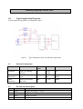
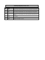
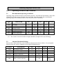
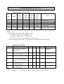
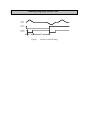
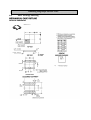
USER MANUAL
DualMag™
Dual Track MagStripe
Decoding ASIC
80053505-001-B
01-09-2012
DualMag MagStripe Decode ASIC
LIMITED WARRANTY
ID TECH warrants to the original purchaser for a period of 12 months from the date of invoice that
this product is in good working order and free from defects in material and workmanship under
normal use and service. ID TECH’s obligation under this warranty is limited to, at its option,
replacing, repairing, or giving credit for any product, which has within the warranty period, been
returned to the factory of origin, transportation charges and insurance prepaid, and which is, after
examination, disclosed to ID TECH’s satisfaction to be thus defective. The expense of removal
and reinstallation of any item or items of equipment is not included in this warranty. No person,
firm, or corporation is authorized to assume for ID TECH any other liabilities in connection with
the sales of any product. In no event shall ID TECH be liable for any special, incidental or
consequential damages to purchaser or any third party caused by any defective item of equipment,
whether that defect is warranted against or not. Purchaser’s sole and exclusive remedy for
defective equipment, which does not conform to the requirements of sales, is to have such
equipment replaced or repaired by ID TECH. For limited warranty service during the warranty
period, please contact ID TECH to obtain a Return Material Authorization (RMA) number &
instructions for returning the product.
THIS WARRANTY IS IN LIEU OF ALL OTHER WARRANTIES OF MERCHANTABILITY
OR FITNESS FOR PARTICULAR PURPOSE. THERE ARE NO OTHER WARRANTIES OR
GUARANTEES, EXPRESS OR IMPLIED, OTHER THAN THOSE HEREIN STATED. THIS
PRODUCT IS SOLD AS IS. IN NO EVENT SHALL ID TECH BE LIABLE FOR CLAIMS
BASED UPON BREACH OF EXPRESS OR IMPLIED WARRANTY OF NEGLIGENCE OF
ANY OTHER DAMAGES WHETHER DIRECT, IMMEDIATE, FORESEEABLE,
CONSEQUENTIAL OR SPECIAL OR FOR ANY EXPENSE INCURRED BY REASON OF
THE USE OR MISUSE, SALE OR FABRICATIONS OF PRODUCTS WHICH DO NOT
CONFORM TO THE TERMS AND CONDITIONS OF THE CONTRACT.
The information contained herein is provided to the user as a convenience. While every effort has
been made to ensure accuracy, ID TECH is not responsible for damages that might occur because
of errors or omissions, including any loss of profit or other commercial damage, nor for any
infringements or patents or other rights of third parties that may result from its use. The
specifications described herein were current at the time of publication, but are subject to change at
any time without prior notice.
ID TECH is a registered trademark of International Technologies & Systems Corporation.
DualMag and Value through Innovation are trademarks of International Technologies & Systems
Corporation.
ID TECH
10721 Walker Street
Cypress, CA 90630
(714)761-6368
DualMag MagStripe Decode ASIC
Revision History
Rev. Date
Description
By
A
2011/06/22 Initial release
JW
B
2012/01/09 Corrected package dimension
JW
Table of Contents
1.0 Introduction ............................................................................................................................... 4
2.0 Features ..................................................................................................................................... 4
3.0 General Functional Description ................................................................................................ 5
3.1
Functional Overview – Architectural Block Diagram ........................................................ 6
4.0 Typical Application Diagrams .................................................................................................. 7
4.1
External Components .......................................................................................................... 7
4.2
Pin Function Description .................................................................................................... 7
5.0 Operating Parameters and Conditions ...................................................................................... 9
5.1
Recommended Operating Conditions ................................................................................. 9
5.2
Absolute Maximum Ratings ............................................................................................... 9
5.3
Output Pin DC Characteristics .......................................................................................... 10
5.4
Output Signal Timing ....................................................................................................... 10
6.0 ASIC Package Drawing .......................................................................................................... 12
DualMag MagStripe Decode ASIC
1.0
Introduction
DualMag provides two Magnetic Stripe decode channels in a very compact 3x3 mm QFN12
package. The decoding operations are fully contained with no external decoding components
required. Magnetic Stripe signals from 3mVpp to 1Vpp are read using a fast, adaptive AGC that
compensates for real-world cards with magnetic or mechanical stripe damage. F2F data rates
equivalent to media speeds from three to one hundred inches per second can be easily decoded.
The powerful decoding algorithms compensate for typical problems such as dropout, skew, low
amplitude, jitter, stripe noise, and bias. There are Data and corresponding Clock outputs for each
magnetic stripe track input. There is a single Media Detect output common to the two decoding
circuits.
2.0
Features
•
•
•
•
•
•
•
•
•
•
•
•
•
Fully Compatible with ISO-7811standard
State-of-the-art mixed signal ASIC
Compact, 3x 3 mm QFN12 package
Easily decodes “real world” cards from 30% to 200% of the standard amplitude
Reads data from card swipe speeds from 3 to 100 IPS
Supply voltages from 2.7 to 3.6V
Operating temperature range from -40°C to +85°C
Low power idle current <60µA
Low power operation during read decoding <0.9mA
Automated internal head compensation to support most head types
Automatic Gain Control for magnetic signal range from 3mV to 1V
High immunity to ambient electronic noise
RoHS compliant
DualMag MagStripe Decode ASIC
3.0
General Functional Description
The DualMag ASIC has two identical decode channels. Each channel has two input pins connected
to each magnetic head track.
Two analog signal paths use a separate Signal Detect block. The positive peaks are detected by a
low-offset comparator which then triggers the digital block to wake up the remainder of the signal
path. The minimum signal detect threshold is 3mVpp. When the signal presents on the input pin is
less than the threshold, the chip will be put in the idle mode, and the standby current is less than 60
µA.
The full differential signal is amplified by an AGC block. The AGC is a differential amplifier
which has very high common noise immunity. The control for the AGC comes from the digital.
The default gain will be 128, and it will be adjusted only in steps of 0.5 or 2. The output from the
AGC is monitored for polarity, then rectified to produce a series of peaks from the previously
bipolar input data. A peak detection block is used to track the peaks, allowing each to be compared
to the previous. This serves to help determine true transitions from false, as well as serving as a
basis for the AGC Gain control and peak detect threshold control. The peak detection starts to
track the peak only when the signal level is over the threshold for suppressing the base noise.
The track processing block receives the peak time, uses as bit bound, measures the bit width,
compares current bit width with the average of the previous bit width, performs F2F decode, and
stores the decoded data into a FIFO buffer. The track processing block adjusts the AGC Gain and
Peak detect threshold based on the comparison result of the current peak amplitude to the previous
peak amplitude which is received from the analog block.
The FIFO block buffers the decoded data and streams the data out in the DATA/CLOCK/MD
format. Figure 3 is DATA/CLOCK timing drawing. The falling edge of CLOCK clocking out a bit
of data, the interval of CLOCK matches the bit width, the duty cycle of CLOCK is 0.5. In the
DATA signal, the HIGH level represents data bit ‘0’, the LOW lever represents data bit ‘1’. The
MD signal indicates the magnetic media is detected. It is normal HIGH, active LOW which can be
used by microcontroller to start/stop sampling. The MD is open drain output with weak internal
pull up which will be turned off when internally pull to LOW for saving current. It can be tied
together to microcontroller for multiple DualMag application.
DualMag MagStripe Decode ASIC
3.1
Functional Overview – Architectural Block Diagram
Figure 1
DualMag Block Diagram
DualMag MagStripe Decode ASIC
4.0
Typical Application Diagrams
Typical application diagrams for MagStripe readers
Figure 2
4.1
Typical Magnetic Stripe Card Reader Application
External Components
Component
Function
Nominal
Value
Tolerance
Capacitor
VDD3 de-coupling
capacitor
0.1
-20%,
+20%
µF
Head
Inductance
Head Inductance (per
track)
100
+30
-60
mH (at 1kHz, 100µA
RMS)
Head
Resistance
Head DC Resistance
(per track)
280
+/-30
Ohms
4.2
Units
Pin Function Description
Pin#
Name
Description
1
HDA1
Magnetic head input 1, track A
2
HDA2
Magnetic head input 2, track A
3
VSS
Ground connection
4
TEST_EN
Test pin. Tie to VSS when in normal operation mode.
DualMag MagStripe Decode ASIC
Pin#
Name
Description
5
CK1
Track A Clock, Normal HIGH, active LOW, Falling edge clocking DATA
6
DA1
Track A Data, LOW: Data bit ‘1’; HIGH: Data bit ‘0’
7
DA2
Track B Data, Normal HIGH, active LOW, Falling edge clocking DATA.
8
CK2
Track B Clock, LOW: Data bit ‘1’; HIGH: Data bit ‘0’.
9
MD
Media Detect. Normal HIGH, active LOW, Open drain with internal weak
pull up
10
VDD3
3.3V Supply
11
HDB2
Magnetic head input 2, track B.
12
HDB1
Magnetic head input 1, track B.
DualMag MagStripe Decode ASIC
5.0
Operating Parameters and Conditions
5.1
Recommended Operating Conditions
Operating ranges define the limits for functional operation. Note that the functionality of the ASIC
outside the operating ranges described is not warranted. Operating outside the recommended
operating ranges for extended periods of time may affect device reliability.
SYMBO
L
VDD3
PARAMETER
DC Supply
MIN
TYP
MAX
UNITS
2.7
3.3
3.6
V
NOTES
Iddd
Dynamic Current
0.9
1.5
mA
(1)
Idds
Standby Current
60
75
µA
(1)
VSS
Analog Ground
0
V
Ta
Ambient Temperature
-40
85
C
Tj
Junction Temperature
-40
90
C
Notes:
(1)
The current is measured with all outputs unloaded, all inputs driven (not floating).
5.2
Absolute Maximum Ratings
Stresses above those listed may cause immediate and permanent device failure. It is not implied
that more that one of these conditions can be applied simultaneously.
SYMBOL
VDD
PARAMETER
DC Supply Voltage
MIN
MAX
UNITS
-0.3
3.7
V
Vin
Input Pin Voltage
VSS-0.3
VDD3+0.3
V
Iin
Input Pin Current
-10
10
mA
Tstrg
Storage Temperature
-55
150
C
Tlead
Lead Temperature
N/A
260
C
ESD
ESD overstress immunity
+/- 4KV
NOTES
HBM Mode
Direct
Contact
DualMag MagStripe Decode ASIC
5.3
Pin
Output Pin DC Characteristics
Name
Vol
(max)
Voh
(min)
Iol
(max)
Ioh
(max)
Volts
Volts
mA
mA
(1)
(1)
(1)
(1)
Notes
5
CK1
0.4V
0.8*VDD
-4mA
4mA
Push-pull output
6
DA1
0.4V
0.8*VDD
-4mA
4mA
Push-pull output
7
DA2
0.4V
0.8*VDD
-4mA
4mA
Push-pull output
8
CK2
0.4V
0.8*VDD
-4mA
4mA
Push-pull output
9
MD
0.4V
0.8*VDD
-4mA
4mA
Open drain output with weak
internal pull up (2)
Notes:
(1) Iil and Iih are tested at Vdd = VDDmax Volts
Vol, Iol are tested at Vdd = VDDmin volts
Voh, Ioh are tested at Vdd = VDDmin volts
Direction of current: (+) for sinking and (-) for sourcing
(2) The weak pull up is10k ohms +/- 50%, turned off when pulled down internally.
5.4
Output Signal Timing
Symbol
Description
Tb
Bit duration: the time between
adjacent peaks from the
magnetic head
ts
Setup Time: DATA change to
CLOCK Falling Edge
2
tw
CLOCK Pulse Width
0.5*
Tb
nMDL
Number of Bit-Cells between
“wake-up” and Falling Edge of
MD
tMDL
Falling edge of MD to first
CLOCK falling edge
2
tMDH
Last CLOCK rising edge to
rising edge of MD
tw
Notes:
Tb (µs) = 106/ S*BD
Min
Typ
Max
Units
Note
Swipe speed
depend on
(1)
µs
50% duty cycle
6
µs
S: Swipe speed, IPS; BD: Bit Density, 75 BPI or 210 BPI.
DualMag MagStripe Decode ASIC
SIGNAL
INPUT
DATA
OUTPUT
STROBE
OUTPUT
tw
th
ts
Figure 3
DATA/CLOCK Timing
DualMag MagStripe Decode ASIC
6.0
ASIC Package Drawing