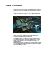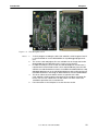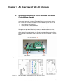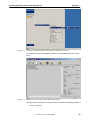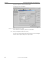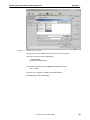
1
User's Manual
MC-CPU-78K0RIC3 CPU
Daughter Card
For use with the Low Voltage Motor Control
Starter Kit
Document No. U19825EE1V0UM00
Date published June 2009
© NEC Electronics 2009
Printed in Germany
Legal Notes
2
•
The information in this document is current as of May, 2008. The
information is subject to change without notice. For actual
design-in, refer to the latest publications of NEC Electronics
data sheets or data books, etc., for the most up-to-date
specifications of NEC Electronics products. Not all products
and/or types are available in every country. Please check with
an NEC Electronics sales representative for availability and
additional information.
•
No part of this document may be copied or reproduced in any form
or by any means without the prior written consent of NEC
Electronics. NEC Electronics assumes no responsibility for any
errors that may appear in this document.
•
NEC Electronics does not assume any liability for infringement of
patents, copyrights or other intellectual property rights of third
parties by or arising from the use of NEC Electronics products listed
in this document or any other liability arising from the use of such
products. No license, express, implied or otherwise, is granted under
any patents, copyrights or other intellectual property rights of NEC
Electronics or others.
•
Descriptions of circuits, software and other related information in this
document are provided for illustrative purposes in semiconductor
product operation and application examples. The incorporation of
these circuits, software and information in the design of a customer's
equipment shall be done under the full responsibility of the customer.
NEC Electronics assumes no responsibility for any losses incurred
by customers or third parties arising from the use of these circuits,
software and information.
•
While NEC Electronics endeavors to enhance the quality, reliability
and safety of NEC Electronics products, customers agree and
acknowledge that the possibility of defects thereof cannot be
eliminated entirely. To minimize risks of damage to property or injury
(including death) to persons arising from defects in NEC Electronics
products, customers must incorporate sufficient safety measures in
their design, such as redundancy, fire-containment and anti-failure
features.
•
NEC Electronics products are classified into the following three
quality grades: "Standard", "Special" and "Specific".
•
The "Specific" quality grade applies only to NEC Electronics
products developed based on a customer-designated "quality
assurance program" for a specific application. The recommended
applications of an NEC Electronics product depend on its quality
grade, as indicated below. Customers must check the quality grade
of each NEC Electronics product before using it in a particular
application.
"Standard": Computers, office equipment, communications
equipment, test and measurement equipment, audio and visual
equipment, home electronic appliances, machine tools, personal
electronic equipment and industrial robots.
"Special": Transportation equipment (automobiles, trains, ships,
etc.), traffic control systems, anti-disaster systems, anti-crime
User's Manual U19825EE1V0UM00
systems, safety equipment and medical equipment (not specifically
designed for life support).
"Specific": Aircraft, aerospace equipment, submersible repeaters,
nuclear reactor control systems, life support systems and medical
equipment for life support, etc.
The quality grade of NEC Electronics products is "Standard" unless otherwise
expressly specified in NEC Electronics data sheets or data books, etc. If
customers wish to use NEC Electronics products in applications not intended by
NEC Electronics, they must contact an NEC Electronics sales representative in
advance to determine NEC Electronics' willingness to support a given application.
(Note)
(1) "NEC Electronics" as used in this statement means NEC Electronics
Corporation and also includes its majority-owned subsidiaries.
(2) "NEC Electronics products" means any product developed or manufactured
by or for NEC Electronics (as defined above).
User's Manual U19825EE1V0UM00
3
Notes for CMOS Devices
4
1.
VOLTAGE APPLICATION WAVEFORM AT INPUT PIN
Waveform distortion due to input noise or a reflected wave may
cause malfunction. If the input of the CMOS device stays in the area
between VIL (MAX) and VIH (MIN) due to noise, etc., the device may
malfunction. Take care to prevent chattering noise from entering the
device when the input level is fixed, and also in the transition period
when the input level passes through the area between VIL (MAX) and
VIH (MIN).
2.
HANDLING OF UNUSED INPUT PINS
Unconnected CMOS device inputs can result in malfunction. If an
input pin is unconnected, it is possible that an internal input level may
be generated due to noise, etc., causing malfunction. CMOS devices
behave differently than Bipolar or NMOS devices. Input levels of
CMOS devices must be fixed high or low by using pull-up or pulldown circuitry. Each unused pin should be connected to VDD or
GND via a resistor if there is a possibility that it will be an output pin.
All handling related to unused pins must be judged separately for
each device and according to related specifications governing the
device.
3.
PRECAUTION AGAINST ESD
A strong electric field, when exposed to a MOS device, can cause
destruction of the gate oxide and ultimately degrade the device
operation. Steps must be taken to stop generation of static electricity
as much as possible, and to quickly dissipate it should it occur.
Environmental control must be adequate. When it is dry, a humidifier
should be used. It is recommended to avoid using insulators that
easily build up static electricity. Semiconductor devices must be
stored and transported in an anti-static container, static shielding
bag or conductive material. All test and measurement tools including
work benches and floors should be grounded. The operator should
be grounded using a wrist strap. Semiconductor devices must not
be touched with bare hands. Similar precautions need to be taken
for PW boards with mounted semiconductor devices.
4.
STATUS BEFORE INITIALIZATION
Power-on does not necessarily define the initial status of a MOS
device. Immediately after the power source is turned ON, devices
with reset functions have not yet been initialized. Hence, power-on
does not guarantee output pin levels, I/O settings or contents of
registers. A device is not initialized until the reset signal is received.
A reset operation must be executed immediately after power-on for
devices with reset functions.
5.
POWER ON/OFF SEQUENCE
In the case of a device that uses different power supplies for the
internal operation and external interface, as a rule, switch on the
external power supply after switching on the internal power supply.
When switching the power supply off, as a rule, switch off the
external power supply and then the internal power supply. Use of the
reverse power on/off sequences may result in the application of an
overvoltage to the internal elements of the device, causing
malfunction and degradation of internal elements due to the passage
of an abnormal current. The correct power on/off sequence must be
User's Manual U19825EE1V0UM00
judged separately for each device and according to related
specifications governing the device.
6.
INPUT OF SIGNAL DURING POWER OFF STATE
Do not input signals or an I/O pull-up power supply while the device
is not powered. The current injection that results from input of such
a signal or I/O pull-up power supply may cause malfunction and the
abnormal current that passes in the device at this time may cause
degradation of internal elements. Input of signals during the power
off state must be judged separately for each device and according
to related specifications governing the device.
User's Manual U19825EE1V0UM00
5
Regional Information
Some information contained in this document may vary from country to country. Before
using any NEC product in your application, please contact the NEC office in your country
to obtain a list of authorized representatives anddistributors. They will verify:
•
Device availability
•
Ordering information
•
Product release schedule
•
Availability of related technical literature
•
Development environment specifications (for example, specifications for
third-party tools and components, host computers, power plugs, AC
supply voltages, and so forth)
•
Network requirements
In addition, trademarks, registered trademarks, export restrictions, and otherlegal
issues may also vary from country to country.
NEC Electronics Corporation
1753, Shimonumabe, Nakahara-ku,
Kawasaki, Kanagawa 211-8668, Japan
Tel: 044 4355111
http://www.necel.com/
[America]
[Europe]
[Asia & Oceania]
NEC Electronics America, Inc.
2880 Scott Blvd.
Santa Clara, CA 95050-2554,
U.S.A.
Tel: 408 5886000
http://www.am.necel.com/
NEC Electronics (Europe) GmbH
Arcadiastrasse 10
40472 Düsseldorf, Germany
Tel: 0211 65030
http://www.eu.necel.com/
NEC Electronics (China) Co., Ltd
7th Floor, Quantum Plaza, No. 27
ZhiChunLu Haidian District,
Beijing 100083, P.R.China
Tel: 010 82351155
http://www.cn.necel.com/
United Kingdom Branch
Cygnus House, Sunrise Parkway
Linford Wood, Milton Keynes
MK14 6NP, U.K.
Tel: 01908 691133
Succursale Française
9, rue Paul Dautier, B.P. 52
78142 Velizy-Villacoublay Cédex
France
Tel: 01 30675800
Tyskland Filial
Täby Centrum
Entrance S (7th floor)
18322 Täby, Sweden
Tel: 08 6387200
Filiale Italiana
Via Fabio Filzi, 25/A
20124 Milano, Italy
Tel: 02 667541
Branch The Netherlands
Steijgerweg 6
5616 HS Eindhoven,
The Netherlands
Tel: 040 2654010
NEC Electronics Shanghai Ltd.
Room 2511-2512, Bank of China
Tower,
200 Yincheng Road Central,
Pudong New Area,
Shanghai 200120, P.R. China
Tel: 021 58885400
http://www.cn.necel.com/
NEC Electronics Hong Kong Ltd.
12/F., Cityplaza 4,
12 Taikoo Wan Road, Hong Kong
Tel: 2886 9318
http://www.hk.necel.com/
NEC Electronics Taiwan Ltd.
7F, No. 363 Fu Shing North Road
Taipei, Taiwan, R.O.C.
Tel: 02 27192377
NEC Electronics Singapore Pte. Ltd.
238A Thomson Road,
#12-08 Novena Square,
Singapore 307684
Tel: 6253 8311
http://www.sg.necel.com/
NEC Electronics Korea Ltd.
11F., Samik Lavied’or Bldg., 720-2,
Yeoksam-Dong, Kangnam-Ku, Seoul,
135-080, Korea Tel: 02-558-3737
http://www.kr.necel.com/
6
User's Manual U19825EE1V0UM00
Preface
Readers
This manual is intended for users who want to understand the functions of the
MC-CPU-78K0RIC3 CPU Daughter Card for motor control.
Purpose
This manual presents the hardware manual of the MC-CPU-78K0RIC3 for motor
control.
Organization
This system specification describes the following sections:
•
•
•
Legend
Symbols and notation are used as follows:
•
•
•
Note
Jumper Descriptions
Hardware Setup
Schematics
Weight in data notation: Left is high order column, right is low order
column
Active low notation: xxx (pin or signal name is over-scored) or /xxx
(slash before signal name)
Memory map address: High order at high stage and low order at low
stage
Additional remark or tip; explanation of (Note) in the text
Caution
Item deserving extra attention
Remark
Supplementary explanation to the text
Numeric Notation
Prefixes
•
•
•
Binary: xxxx or xxxB
Decimal: xxxx
Hexadecimal: xxxxH or 0x xxxx
representing powers of 2 (address space, memory capacity):
•
•
•
K (kilo): 210 = 1024
M (mega): 220 = 10242 = 1,048,576
G (giga): 230 = 10243 = 1,073,741,824
User's Manual U19825EE1V0UM00
7
Table of Contents
Chapter 1
Introduction
Chapter 2
MC-CPU-78K0RIC3 CPU Daughter Card
Specifications . . . . . . . . . . . . . . . . . . . . . . . . . . . . . . . . . . . . . . . . . . . . . . . . . . . . .
12
An Overview of MC-IO Interface . . . . . . . . . . . . . . . . . . . . . . . . . . . .
13
Chapter 3
. . . . . . . . . . . . . . . . . . . . . . . . . . . . . . . . . . . . . . . . . . . . . . . . . . . . . . . 10
3.1
General Descriptions of MC-IO Interface with Motor Control Micro-Boards . . . . . . . . . . . 13
3.2
Motor Control Interface Signals . . . . . . . . . . . . . . . . . . . . . . . . . . . . . . . . . . . . . . . . . . . . . . . . . . . . 14
3.3
Signal Positions on the 100-pin Connectors . . . . . . . . . . . . . . . . . . . . . . . . . . . . . . . . . . . . . . . . . 15
Chapter 4
MC-CPU-78K0RIC3 Hardware Design Descriptions
. . . . . . . . . . . . . . . . . . . . . . . . . . . . . . . . . . . . . . . . . . . . . . . . . . . . . . . . . . . . . . . . . . . . . . . . . . 17
4.1
An Overview of Signal Connections for the MC-CPU-78K0RIC3 CPU Daughter Card . . . 17
4.2
Power Source Selection . . . . . . . . . . . . . . . . . . . . . . . . . . . . . . . . . . . . . . . . . . . . . . . . . . . . . . . . . . . 17
4.3
Reset Generation . . . . . . . . . . . . . . . . . . . . . . . . . . . . . . . . . . . . . . . . . . . . . . . . . . . . . . . . . . . . . . . . . 18
4.4
FLMD0 - Flash Programming Mode Setting Signal . . . . . . . . . . . . . . . . . . . . . . . . . . . . . . . . . . 19
4.5
16P_FLASHDEBUG_HEADER . . . . . . . . . . . . . . . . . . . . . . . . . . . . . . . . . . . . . . . . . . . . . . . . . . . . . . 20
4.6
Main Clock and Sub-Clock . . . . . . . . . . . . . . . . . . . . . . . . . . . . . . . . . . . . . . . . . . . . . . . . . . . . . . . . . 21
4.7
Target System Connector . . . . . . . . . . . . . . . . . . . . . . . . . . . . . . . . . . . . . . . . . . . . . . . . . . . . . . . . . 21
4.8
Optional RS232-UART Connections . . . . . . . . . . . . . . . . . . . . . . . . . . . . . . . . . . . . . . . . . . . . . . . . 22
4.9
LED Data Loading . . . . . . . . . . . . . . . . . . . . . . . . . . . . . . . . . . . . . . . . . . . . . . . . . . . . . . . . . . . . . . . . . 23
4.9.1
MC-CPU-78K0RIC3 Port Assignments for LED Segment Data . . . . . . . . . . . . . . . . . 23
4.9.2
MC-CPU-78K0RIC3 Port Signal Assignments for LED Data Load Control . . . . . . . . 24
4.10
Comparator/Hall Sensor and Motor Position Encoder Signal Inputs for µPD78K0R-IC3 24
...................................................................................
4.11
Motor Speed Measurement . . . . . . . . . . . . . . . . . . . . . . . . . . . . . . . . . . . . . . . . . . . . . . . . . . . . . . . . 24
4.12
Use of Signals: Signal Assignments and Signal Multiplexing . . . . . . . . . . . . . . . . . . . . . . . . . . 25
4.13
Optional Selection for P80_P80/CMP0P/OA1 and P82_P82/Comparator Input . . . . . . . . . 27
Chapter 5
Flash Programming with a Flash Programmer
. . . . . . . . 28
5.1
Download the Following Files . . . . . . . . . . . . . . . . . . . . . . . . . . . . . . . . . . . . . . . . . . . . . . . . . . . . . . 29
5.2
Save and Uncompress the IAR Workbench Project . . . . . . . . . . . . . . . . . . . . . . . . . . . . . . . . . . 29
5.3
Switch Settings and Connecting the MINICUBE2 . . . . . . . . . . . . . . . . . . . . . . . . . . . . . . . . . . . . 29
5.4
To program the MC-CPU-78K0RIC3 while not connected to the MC-IO module . . . . . . . . 35
Chapter 6
Operation of the MC-CPU-78K0RIC3
. . . . . . . . . . . . . . . . . . . . . 36
6.1
MC-CPU-78K0RIC3 in Standalone Operation . . . . . . . . . . . . . . . . . . . . . . . . . . . . . . . . . . . . . . . .
6.1.1
CPU Daughter Card Jumper Settings . . . . . . . . . . . . . . . . . . . . . . . . . . . . . . . . . . . . . . . .
6.1.2
Operation . . . . . . . . . . . . . . . . . . . . . . . . . . . . . . . . . . . . . . . . . . . . . . . . . . . . . . . . . . . . . . . .
6.1.3
Drive and Motor Protection . . . . . . . . . . . . . . . . . . . . . . . . . . . . . . . . . . . . . . . . . . . . . . . . .
36
36
36
38
6.2
MC-CPU-78K0RIC3 in GUI Operation . . . . . . . . . . . . . . . . . . . . . . . . . . . . . . . . . . . . . . . . . . . . . . .
6.2.1
GUI Software Installation . . . . . . . . . . . . . . . . . . . . . . . . . . . . . . . . . . . . . . . . . . . . . . . . . . .
6.2.2
To Use GUI Software . . . . . . . . . . . . . . . . . . . . . . . . . . . . . . . . . . . . . . . . . . . . . . . . . . . . . .
6.2.3
Set the Serial Port Number . . . . . . . . . . . . . . . . . . . . . . . . . . . . . . . . . . . . . . . . . . . . . . . . .
6.2.4
Run the Motor Using Speed Control Mode . . . . . . . . . . . . . . . . . . . . . . . . . . . . . . . . . . .
6.2.5
Change the PID Settings . . . . . . . . . . . . . . . . . . . . . . . . . . . . . . . . . . . . . . . . . . . . . . . . . . .
6.2.6
Change the Setup Settings . . . . . . . . . . . . . . . . . . . . . . . . . . . . . . . . . . . . . . . . . . . . . . . . .
38
39
40
42
43
43
45
8
User's Manual U19825EE1V0UM00
6.2.7
Chapter 7
Change the Startup Settings . . . . . . . . . . . . . . . . . . . . . . . . . . . . . . . . . . . . . . . . . . . . . . . . 46
MC-CPU-78K0RIC3 with IAR Embedded Workbench
. . . . . . . . . . . . . . . . . . . . . . . . . . . . . . . . . . . . . . . . . . . . . . . . . . . . . . . . . . . . . . . . . . . . . . . . . . 48
7.1
Software Installation . . . . . . . . . . . . . . . . . . . . . . . . . . . . . . . . . . . . . . . . . . . . . . . . . . . . . . . . . . . . . . 48
7.2
Switch Settings and Connecting the MINICUBE2 . . . . . . . . . . . . . . . . . . . . . . . . . . . . . . . . . . . . 48
7.3
IAR Embedded Workbench Startup . . . . . . . . . . . . . . . . . . . . . . . . . . . . . . . . . . . . . . . . . . . . . . . . . 49
7.4
General Options . . . . . . . . . . . . . . . . . . . . . . . . . . . . . . . . . . . . . . . . . . . . . . . . . . . . . . . . . . . . . . . . . . 52
7.5
Compiler Options . . . . . . . . . . . . . . . . . . . . . . . . . . . . . . . . . . . . . . . . . . . . . . . . . . . . . . . . . . . . . . . . . 55
7.6
Assembler Options . . . . . . . . . . . . . . . . . . . . . . . . . . . . . . . . . . . . . . . . . . . . . . . . . . . . . . . . . . . . . . . . 58
7.7
Linker Options . . . . . . . . . . . . . . . . . . . . . . . . . . . . . . . . . . . . . . . . . . . . . . . . . . . . . . . . . . . . . . . . . . . . 60
7.8
Integrated Debugger Selection . . . . . . . . . . . . . . . . . . . . . . . . . . . . . . . . . . . . . . . . . . . . . . . . . . . . . 63
7.9
Workspace and Project Setup if Not Compatible with the Installed IAR Workbench . . . . 64
7.10
Build/Rebuild the Project . . . . . . . . . . . . . . . . . . . . . . . . . . . . . . . . . . . . . . . . . . . . . . . . . . . . . . . . . . 65
7.11
Debugging . . . . . . . . . . . . . . . . . . . . . . . . . . . . . . . . . . . . . . . . . . . . . . . . . . . . . . . . . . . . . . . . . . . . . . . . 65
Chapter 8
Appendix . . . . . . . . . . . . . . . . . . . . . . . . . . . . . . . . . . . . . . . . . . . . . . . . . . . . . . . . . . . .
User's Manual U19825EE1V0UM00
71
9
Chapter 1 Introduction
The MC-CPU-78K0RIC3 CPU Daughter Card is designed to form part of the lowvoltage starter kit for motor control (MC-LVKIT-78K0RIC3) and is a complete 3phase motor control evaluation system for NEC Electronics’ microcontroller
application-specific standard products (ASSP’s) for motor control.
The MC-CPU-78K0RIC3 kit contains all necessary hardware and software to
quickly set up and run a low-voltage brushless DC motor (BLDCM).
Figure 1-1
MC-LVKIT 3 phase Motor Control Evaluation System
The MC-CPU-78K0RIC3 CPU Daughter Card is used to demonstrate and
evaluate CPU and on-chip peripheral functions of NEC Electronics16-bit
microcontrollers, µPD78K0R-IE3 and µPD78K0R-IC3.
The MC-CPU-78K0RIC3 CPU Daughter Card will interface with the Motor Control
I/O Board (MC-I/O Board), in motor control applications. In addition, the MCCPU-78K0RIC3 supports Flash programming and debugging when the CPU
Daughter Card is connected to a host-PC through the MINICUBE2 on-chip
debugger/programmer.
In order to provide sufficient details for the users to interface with MC-I/O Board,
some details for both MC-I/O board and the MC-CPU-78K0RIC3 CPU Daughter
Card will be provided in this manual.
Please see the MC-CPU-78K0RIC3 CPU Daughter Card below:
10
User's Manual U19825EE1V0UM00
Introduction
Chapter 1
Figure 1-2
Notes
CPU Daughter Card
1.
2.
3.
4.
5.
To flash program or debug the MC-CPU-78K0RIC3 CPU Daughter Card it
is recommended to use the MINICUBE2 on-chip debugger/programmer
unit.
The source code and project files are available free of charge and can be
downloaded from the NEC Electronics motor control website.
In order to modify the source code, the IAR development environment is
required and a time limited version can be acquired directly from the IAR
website or a code limited trial version is included in the MINICUBE2 on-chip
debugger/programmer or the full IAR development tool can be purchased
from NEC Electronics or through an NEC Electronics franchised distributor.
This User's Manual covers details which are specific to the MCCPU-78K0RIC3 CPU Daughter Card and not the complete evaluation kit.
Please see the User's Manual for the MC-LVKIT-714 which covers the
standalone operation of the evaluation kit.
For information on the GUI please see the relevant section.
User's Manual U19825EE1V0UM00
11
Chapter 2 MC-CPU-78K0RIC3 CPU Daughter Card
Specifications
The MC-CPU-78K0RIC3 CPU Daughter Card supports uPD78K0R-IE3 and
uPD78K0R-IC3 microcontrollers. The specifications for these microcontrollers
are:
µPD78K0R-Ix3 Features
Flash Self-Programming (with Boot Swap Function/Flash Shield Window
Function)
Built In On-chip Functions
•
•
•
•
•
On-chip Debugging Function
On-chip Power-on Clear
On-chip Watchdog Timer
On-chip Multiplier/Divider
On-chip BCD Adjustment
I/O Ports
Timer (TAU)
•
•
•
12 channel x 16-bit @ 40 MHz TAU (Timer Array Unit)
Watchdog Timer
On-chip Motor Control Option Unit
On-Chip Comparator/Operational Amplifier
Serial Interface (SAU)
•
•
•
UART (LIN)
CSI
Simplified I²C
10-Bit Resolution A/D Converters @ 2.5uS conversion time
Power Supply Voltage
•
12
VDD = 2.7 VDC - 5.5 VDC
User's Manual U19825EE1V0UM00
Chapter 3 An Overview of MC-IO Interface
3.1 General Descriptions of MC-IO Interface with Motor
Control Micro-Boards
The MC-CPU-78K0RIC3 CPU Daughter Card provides controller functions for
motor control operation. It processes and determines microcontroller actions
from various sensor inputs. The Motor Control Evaluation System consists of:
•
•
•
Power Module (MC-PWR-LV)
Motor Control I/O Module (MC-I/O)
MC-CPU-78K0RIC3 CPU Daughter Card (this product)
The power module (MC-PWR-LV) drives the motor and provides sense signals
through the 40-pin ribbon cable (J5). The MC-I/O board sends and receives
signals to the power module via the 40-pin ribbon cable at (J4) and the 14-pin
terminal block at (J5) and provides user interface and operation control functions.
The removable CPU Daughter Card is connected to the MC-I/O board, as shown
below.
Figure 3-1
MC-CPU-78K0RIC3 installed on MC-IO Board
Figure 3-2
MC-IO and MC-CPU-78K0RIC3 CPU Daughter Card
User's Manual U19825EE1V0UM00
13
Chapter 3
An Overview of MC-IO Interface
The MC-CPU-78K0RIC3 CPU Daughter Card control signals use two 100-pin high
density connectors. All control signals are placed on the two interface connectors
at pre-selected positions. This method enables multiple Motor Control CPU
Daughter Cards to interface with the MC-I/O interchangeably. Therefore, it is
important to know the motor control signals used.
This section provides general overview of module interfaces so that users can
become familiar with the system. The next section provides specific information
how the MC-CPU-78K0RIC3 signals are interfacing with the system.
3.2 Motor Control Interface Signals
Table 3-1
Signal on MC-I/O J5 14-Pin Terminal Block
Categories
Signal Names
Description of Signals
Motor Position Encoder
ENC_A, ENC_B, ENC_Z
Motor position encoder signals
connected to interrupt inputs
of CPU
HALL effect sensor input
HALL Effect Sensor Signal HALL_1, HALL_2, HALL_3 connected to interrupt inputs
of CPU
Motor Temperature Input
ANI3_TEMP
Motor temperature input
connected to A/D converter
input of CPU
The signals on 14-pin terminal block are the sensor signals from the motor unit.
These signals are input to microcontroller on the CPU Daughter Card through MCI/O module.
Table 3-2
Signals on MC-I/O J4 40-Pin Ribbon Cable
Categories
System Power
Signal Names
Description of Signals
VCC_15V
Power input to MC-I/O board
VCC_5V
Regulated 5V Power
HI_U, HI_V, HI_W
- High-side FET Drive
PWM Signals
LO_U, LO_V, LO_W
- Low-side FET Drive
Back-EMF Comparator
CMPU, CMPV, CMPW
Back-EMF comparator signals
from power module connected
to interrupt inputs of CPU
ANI0_IU, ANI1_IV,
ANI2_IW
Motor phase current Low-side current detect
connected to A/D
ISHUNT
Motor shunt current Low-side current detect
connected to A/D
PX_ITRIP
Over-current detect signal
from power module connected
to TMOFF0 or TMOFF1 of
78K0RIx3
TRIP
CPU generated signal to turn
off power to Power-MOSFET
Current Sense Signals
Safety Control Signals
14
PWM Signals from CPU
User's Manual U19825EE1V0UM00
An Overview of MC-IO Interface
Chapter 3
Categories
Signal Names
Description of Signals
Phase Voltage Detect
V-U, V-V, V-W
Motor phase voltage detect
signal connected to A/D inputs
of CPU
Power-Module
Temperature
ANI7_TMP
Power module temperature
sense signal connected to
A/D input of CPU
The above signals are coming from power module (MC-PWR-LV) through 40-pin
cable interface. These signals are connected to two 100-pin connectors on the
MC-I/O Board. The microcontroller inputs and outputs are connected to these
signals when the CPU Daughter Card is connected to the MC-I/O board, through
two 100-pin connectors.
3.3 Signal Positions on the 100-pin Connectors
Table 3-3
J1 Pin
1
2
4
J1 Signal
J1.003
RS232_RXD
J1.004
RS232_CTS
J1.005
RS232_TXD
J1.006
RS232-RTS
PX_ITRIP
Notes
Connects to RS232 transceiver interface U23
J4.02
Signal to tri-state Power MOSFETs connect
to TMOFF0 or TMOFF1 on 78K0RIx3
PX_ITRIP
Speed Adjust Potentiometer and other A/D
J1.023
ANI4 (Spd Pot)
J1.024
ANI5_ISHUNT
J4.07
ANI5_ISHUNT
From power module shunt current signal
J1.025
ANI6_SPARE
J4.04
ANI6_SPARE
Spare A/D input
ANI4 adjust speed pot use A/D
PX_TRIPB Signal to turn off power to power MOSFETs
PX_TRIPB
Table 3-4
J2 Pin
6
J4 Signal
PX_ITRIP Signal from Power Module
J1.031
5
J4 Pin
RS232 Host Interface Signals
J1.011
3
Signals on MC-I/O J1-Connector (P1-Connector on MC-CPU-78K0RIC3)
J4.19
Signal from CPU to turn off power to power
MOSFETs. Use GPI/O on 78K0R/Ix3.
TRIP
Signals on MC-I/O J2-Connector (P2-Connector on MC-CPU-78K0RIC3)
J2 Signal
J4 Pin
J4 Signal
J5 Pin
J5 Signal
LD_LED - data latch signals for the 7 segment LED displays
J2.015
LD_LED0
J2.016
LD_LED1
J2.017
LD_LED2
J2.018
LD_LED3
Use GPI/O on 78K0R/
Ix3
LED_x - common data lines for 7 segment LED displays
J2.019
LED_A
J2.020
LED_B
J2.021
LED_C
Use GPI/O on 78K0R/
Ix3
User's Manual U19825EE1V0UM00
15
Chapter 3
7
8
J2 Pin
J2 Signal
J2.022
LED_D
J2.023
LED_E
J2.024
LED_F
J2.025
LED_G
J2.026
LED_DP
11
12
14
16
J5 Pin
J5 Signal
PWM_0
J4.21
HI_U
CPU signal PWM_0
J2.030
PWM_1
J4.27
LO_U
CPU signal PWM_1
J2.033
PWM_2
J4.23
HI_V
CPU signal PWM_2
J2.034
PWM_3
J4.29
LO_V
CPU signal PWM_3
J2.037
PWM_4
J4.25
HI_W
CPU signal PWM_4
J2.038
PWM_5
J4.31
LO_W
CPU signal PWM_5
SPD_MSR - select one from INTP1_PX / INTP2_PY / INTP3_PZ
Timer/counter input for
speed measurement
SPD_MSR
Temperature sense signal from power module
ANI7_TMP
J4.09
ANI7_TMP
INTP1_PX / INTP2_PY / INTP3_PZ to interrupt inputs
J2.047
INTP1_PX
J4.13
CMP_U
INTP1_PX = CMP_U or
V-U or HALL1
J2.048
INTP2_PY
J4.15
CMP_V
INTP2_PY = CMP_V or
V-V or HALL2
J2.051
INTP3_PZ
J4.17
CMP_W
INTP3_PZ = CMP_W or
V-W or HALL3
Phase current sense signals from power module
J2.052
ANI0_IU
J4.01
ANI0_IU
Current Sense Phase U
J2.055
ANI1_IV
J4.03
ANI1_IV
Current Sense Phase V
J2.056
ANI2_IW
J4.05
ANI2_IW
Current Sense Phase W
ANI3_TEMP Motor temperature sense signal
J2.059
13
J4 Signal
J2.029
J2.044
10
J4 Pin
PWM signals - Motor phase control signals IU, IV, IW
J2.041
9
An Overview of MC-IO Interface
ANI3_TEMP
J5.08
ANI3_TEMP
Motor temperature
connect to A/D
Encoder signals - PX_ENCA, PX_ENCB, PX_ENCZ
J2.060
PX_ENCA
J5.11
ENC_A
J2.063
PX_ENCB
J5.10
ENC_B
J2.064
PX_ENCZ
J5.03
ENC_Z
Operation control push buttons
J2.067
START
J2.068
FORWARD
J2.071
REVERSE
J2.072
MODE
GPI/O pins on the
78K0R/Ix3
User's Manual U19825EE1V0UM00
Chapter 4 MC-CPU-78K0RIC3 Hardware Design
Descriptions
4.1 An Overview of Signal Connections for the MCCPU-78K0RIC3 CPU Daughter Card
VDD_KR
(1,3,4,5) VDD_KR
9
1
VDD_KR (1,3,4,5)
SB21
P122/X2/EXCLK/INTP5
REGC
12
REGC (1)
P123/XT1
8
P123_IC3
P124/XT2
7
P124_IC3
P120_IC3
28
27
26
25
24
23
22
P120/INTP0/EXLV1
P30/SO10/TXD1/TO11
P31/SI10/RXD1/SDA10/INTP1
P32/SCK10_B/SCL10/IN
P83/CMP1M
P82/CMP1P/TMOFF1/INT
P81/CMP0M
P80/CMP0P/TMOFF0/INT
P10/TI02/TO02
P11/TI03/TO03
P12/TI04/TO04
P13/TI05/TO05
P50/TI06/TO06
P73/TXD0/TO10
P51/TI07/TO07
P52/SLTI/SLTO
P72/INTP6/RXD0
5
29
30
31
32
P83_P83 (1,3,5)
P82_P82 (1,3,5)
PX_TRIPB (1,3,5)
P80_P80 (1,5)
21
20
P40/TOOL0
P41/TOOL1
P122_IC3
18
RS232_TXD (1,3,5)
19
RS232_RXD (1,3,5)
VSS
15
16
17
P20/ANI0
P21/ANI1
P22/ANI2
P23/ANI3
P24/ANI4
P25/ANI5
P26/ANI6
P27/ANI7
P121_IC3
13
P30_IC3
P31_IC3
P32_IC3
RESET_B
34
Figure 4-1
2
11
4
3
2
1
38
37
36
35
(1,3) TOOL0
(1,3) TOOL1
33
10
P20_IC3
P21_IC3
P22_IC3
P23_IC3
P24_IC3
P25_IC3
P26_IC3
P27_IC3
(1,3,5) PWM_0
(1,3,5) PWM_1
(1,3,5) PWM_2
(1,3,5) PWM_3
(1,3,5) PWM_4
(1,3,5) PWM_5
(1,3,5) P17_P52
AVREF (1)
AVREF
P121/X1/INTP4
6
(1,3) RESETB_KR
FLMD0
AVSS
(1) FLMD0_KR
0.1uF
VDD
uPD78K0R-IC3
C13
14
U5
Signals on µPD78K0RIC3
Special treatment for the REGC signal. REGC is connected to GND through
0.47uF capacitor. Used EIA_A size, tantalum capacitor.
4.2 Power Source Selection
When the MC-CPU-78K0RIC3 CPU Daughter Card is connected to MC-I/O
board, the micro board receives power from the MC-I/O board, VCC_IS
External Power Option
•
•
Use external power connection terminal post TP_EXTVDD
External power may be input to TP_EXTVDD TP_EXTVDD =
2.7 VDC to 5.5 VDC
User's Manual U19825EE1V0UM00
17
Chapter 4
MC-CPU-78K0RIC3 Hardware Design Descriptions
Table 4-1
Power Source Jumper Settings
Power Source Select Jumper
Jumper No.
Connection Descriptions
Description of Functions
JP1
JP1.2 -to- JP1.1
VDD_X = VCC_IS:
Select Power form MC-I/O
Board
JP1.2 -to- JP1.3
VDD_X = EXT_VDD:
Select Externally Supplied
Power
Normally connected
Default Setting is JP2
connected
JP2
CPU Current Measurement:
Connect Ampere Meter on JP2
SBx
EVDD:
Connected to VDD_KR
through 2SB22, Normally
Connected
Solder Jumpers
AVREF:
Connected to VDD_KR
through SB1, Normally
Connected
4.3 Reset Generation
VDD_KR
R8
2
SN74AHC1G08DBVR
10K
5
TGPB_RST
74AHC1G125DBVR
2
3
4
RESETB_X (3)
1
4
R7
U4
0.1uF
5
1
U3
0.1uF
C7
10K
(1) TG_RST
VDD_KR
C6
VDD_KR
3
VDD_KR
VDD_KR
D1
DL4148
PB_RST
R9
R10
10K
+
C8
1UF
Figure 4-2
100
SW1
Micro-Board Reset Generation
Sources of Reset
•
•
Push-button Switch: a Push-Button Reset Switch is provided SW1
Reset from User's Target System TG_RST
RESETB_X
•
•
•
18
RESETB_X is connected to J2, 16P_Flash/Debug_Header
When MINICUBE2 Programmer/Debugger is connected to the it
generates RESETB_KR
When Mini-Cube2 is not connected, RESETB_X is connected to
RESETB_KR by jumper JP6
User's Manual U19825EE1V0UM00
MC-CPU-78K0RIC3 Hardware Design Descriptions
Chapter 4
4.4 FLMD0 - Flash Programming Mode Setting Signal
VDD_KR
C1
U1
74AHC1G126DBVR
5
0.1uF
3
4
1
2
(3) FLMD0
R1
10K
2
1
R2
10K
JP3
P2X1
P83_P83 (2,3,5)
Figure 4-3
FLMD0 – Flash Programming Mode
» In normal operation
FLMD0 Input is pull-down to GND by a
10K-Resistor
» When MINICUBE2 is connected
FLMD0 is driven by MINICUBE2
» For Flash Self-Programming Mode FLMD0 is Driven by P83 of IE3 (P83_P83)
» To use P83_P83 for Mode setting, JP3 should be connected
Table 4-2
FLDM0 Jumper Settings
Jumper Condition
Description of Functions
FLMD0 is driven by MINICUBE2 if connected
JP3
Open
FLMD0 is pulled down by 10K resistor to GND for normal
operation
Connected
During Flash self-programming, FLMD0 can be driven by P83
User's Manual U19825EE1V0UM00
19
Chapter 4
MC-CPU-78K0RIC3 Hardware Design Descriptions
4.5 16P_FLASHDEBUG_HEADER
J2
2
1
TOOL0_QB
JP4
1
3
5
7
9
11
13
15
RXD
TXD
P2X1
2
4
6
8
10
12
14
16
VDD_KR (1,2,4,5)
RESETB_KR (1,2)
FLMD0 (1)
TOOL1_QB
P8X2
JP6
2
(4) RESETB_X
R6
1
10K
P2X1
(1,2) TOOL0
(1,2) TOOL1
4
2
4
2
Table 4-3
3
1
JP8
P 2x2
4
2
3
1
4
2
JP9
Figure 4-4
3
1
3
1
TOOL0_QB
P1_TOOL0
TOOL1_QB
P1_TOOL1
P 2x2
Flash/Debug Header Schematic
Flash/Debug Jumper Settings
JP4
OPEN when Mini-Cube2 has internal connection for RXD and
TXD
OPEN
Other cases (Refer to User's Manual) insert JP4
JP6
OPEN
OPEN when Mini-Cube2 is Connected for Debugging or
Flash Program
Connected
Insert Jumper for Normal Operation
JP8.4 -to- JP8.3
Connect TOOL0 Output to Mini-Cube2 for Debug/Flash
Program
JP8.2 -to- JP8.1
Connect TOOL0 to P1 Connector for Users to use TOOL0 as
Port-pin
JP9.4 -to- JP9.3
Connect TOOL1 Output to Mini-Cube2 for Debug/Flash
Program
JP9.2 -to- JP9.1
Connect TOOL1 to P1 Connector for Users to use TOOL1 as
Port-pin
JP8
JP9
20
User's Manual U19825EE1V0UM00
MC-CPU-78K0RIC3 Hardware Design Descriptions
Chapter 4
4.6 Main Clock and Sub-Clock
VDD_KR
C16
0.1uF
VDD_KR
U9
5
SN74AHC1GU04DBVR
5
U8
2
2
(1) XT2
SN74AHC1GU04DBVR
4
R11
EXCLK_X2 (1)
100
Y2
3
3
4
(1) XT1
32 KHz
R15
BIAS RESISTOR
Y1
C18
18PF
Figure 4-5
C11 MC-405
12PF
2M
20 MHz
HC49US
C12
12PF
R16
100 OHMS
C19
18PF
P122_IC3
JP7
P 3x2
6
4
2
5
3
1
6
4
2
5
3
1
INTP3_PZ (1,3,5)
PX_ENCZ (1,3,5)
EXCLK_X2 (1)
Main Clock and Sub Clock Schematic
A sub-clock oscillator 32 KHz crystal is connected to µPD78K0RIE3 only. The
µPD78K0RIC3 does not use sub-clock (see Signal Assignments and Signal
Multiplexing).
The µPD78K0RIC3 main-clock is selected by JP7. The EXCLK input of
µPD78K0RIC3, P122_IC3, can be used as an interrupt input, receiving comparator
signal or motor position encoder input, when internal clock is used.
JP7 JP7.1 -to- JP7.2 P122_IC3 = EXCLK_X2
JP7.3 -to- JP7.4 P122_IC3 = PX_ENCZ
JP7.5 -to- JP7.6 P122_IC3 = INTP3_PZ
External Clock
Position Encoder Signal
Comparator/HALL Sensor
Signal
4.7 Target System Connector
Figure 4-6
Target System Connector Diagram
Target system connector is provided all around µPD78K0R-IE3 to be connected
to the users' target system. It has same pin outs with µPD78K0R-IE3.
Note
Tthe µPD78K0R-IC3 does not share the target system pins.
User's Manual U19825EE1V0UM00
21
Chapter 4
MC-CPU-78K0RIC3 Hardware Design Descriptions
4.8 Optional RS232-UART Connections
The MC-I/O board provides optional RS232-UART connections to a host-PC. This
section describes RS232 circuit and describes the use of RxD and TxD inputs of
the microcontroller.
Figure 4-7
RS232 Transceiver Circuit on the MC-I/O
On the MC-CPU-78K0RIC3 CPU Daughter Card
•
•
RS232_TXD is the outgoing signal form microcontroller to host-PC
RS232_RXD is the incoming signal from host-PC to microcontroller
Looking from host-PC, transmit output is connected to RXD_DB9. Likewise,
receiving input of the host-PC is connected to TXD_DB9 input. The MCCPU-78K0RIC3 UART inputs and outputs are connected to RS232_RXD and
RS232_TXD according to the above signal directions.
22
User's Manual U19825EE1V0UM00
MC-CPU-78K0RIC3 Hardware Design Descriptions
Chapter 4
4.9 LED Data Loading
The LED data latch is implemented on the MC-I/O board. The MC-CPU-78K0RIE3
assigns port signals for LED data and control signals for latch enable.
Figure 4-8
Table 4-4
LED Data and Load Enable Connections
Port Assignments for for LED-Segment Data
PORT5[3:0]
= LED Segments
LED_A through LED_D
PORT2[3:0]
= LED Segments
LED_E through LED_DP
PORT3[3:2]
= Latch Enable
LED-Digit [1:0]
PORT14[1:0]
= Latch Enable
LED-Digit [3:2]
4.9.1 MC-CPU-78K0RIC3 Port Assignments for LED Segment Data
C15 0.1uF
R12
2
5
11
14
ANI0_IU (1,3,5)
ANI1_IV (1,3,5)
ANI2_IW (1,3,5)
ANI3_TEMP (1,3,5)
1B2
2B2
3B2
4B2
3
6
10
13
LED_A
LED_B
LED_C
LED_D
(1,3,5)
(1,3,5)
(1,3,5)
(1,3,5)
10K
P24_IC3
P25_IC3
P26_IC3
P27_IC3
4
7
9
12
1A
2A
3A
4A
(1,3,5) P83_P83
1
15
S
OE_B
R13
VDD
S
OE_B
SN74CBT3257CPW
1B1
2B1
3B1
4B1
GND
1
15
(TSSOP-16P)
(TSSOP-16P)
1B1
2B1
3B1
4B1
2
5
11
14
ANI4_SPD_POT (1,3,5)
ANI5_ISHUNT (1,3,5)
ANI6_SPARE (1,3,5)
ANI7_TMP (1,3,5)
1B2
2B2
3B2
4B2
3
6
10
13
LED_E (1,3,5)
LED_F (1,3,5)
LED_G (1,3,5)
LED_DP (1,3,5)
8
(1,3,5) P83_P83
VDD
1A
2A
3A
4A
8
4
7
9
12
GND
SN74CBT3257CPW
P20_IC3
P21_IC3
P22_IC3
P23_IC3
16
(1,3,4,5) VDD_KR
U7
16
C14 0.1uF
(1,3,4,5) VDD_KR
U6
10K
When P83_P83 = 1
•
PORT2[7:0] = LED Segments LED_DP through LED_A
When P83_P83 = 0
•
Normal operation state, allowing real-time control signals to be
connected to µPD78K0R-IC3
User's Manual U19825EE1V0UM00
23
Chapter 4
MC-CPU-78K0RIC3 Hardware Design Descriptions
4.9.2 MC-CPU-78K0RIC3 Port Signal Assignments for LED Data Load
Control
C17 0.1uF
(1,3,4,5) VDD_KR
(1,3,5) P83_P83
1A
2A
3A
4A
1
15
S
OE_B
(TSSOP-16P)
1B1
2B1
3B1
4B1
2
5
11
14
PX_START (1,3,5)
PX_FORWARD (1,3,5)
PX_REVERSE (1,3,5)
PX_MODE (1,3,5)
1B2
2B2
3B2
4B2
3
6
10
13
LD_LED0
LD_LED1
LD_LED2
LD_LED3
(1,3,5)
(1,3,5)
(1,3,5)
(1,3,5)
8
R14
VDD
4
7
9
12
GND
P123_IC3
P124_IC3
P30_IC3
P31_IC3
16
U10
SN74CBT3257CPW
10K
When P83_P83 = 1
•
•
PORT12[4;3] = LED latch enable signal LD_LED1 and LD-LED0
PORT3[1:0] = LED latch enable signal LD_LED3 and LD_LED2
When P83_P83 = 0
•
Normal operation state, push-buttons for operation control is
connected to these ports.
4.10 Comparator/Hall Sensor and Motor Position Encoder
Signal Inputs for µPD78K0R-IC3
SB26
1
P120_IC3
SB27
1
SB28
1
P121_IC3
SB29
1
SB30
1
P32_IC3
SB31
1
2
INTP1_PX (1,3,5)
2
PX_ENCA (1,3,5)
2
INTP2_PY (1,3,5)
2
PX_ENCB (1,3,5)
2
INTP3_PZ (1,3,5)
2
PX_ENCZ (1,3,5)
The comparator/hall sensor inputs and motor position encoder signals are
connected directly to the µPD78K0R-IE3. The µPD78K0R-IC3, however, is
required to multiplex the signals. Users must connect solder jumpers for the
selected signals. The INTP1_PX, INTP2_PY and INTP3_PZ are multiplexed signals
between comparator and HALL sensor inputs.
4.11 Motor Speed Measurement
(1,3,5) P17_P52
SB32
1
SB33
1
SB34
1
SB35
1
Figure 4-12
24
2
INTP1_PX (1,3,5)
2
INTP2_PY (1,3,5)
2
INTP3_PZ (1,3,5)
2
FLMD0_KR (1)
Speed Measurement Selection
User's Manual U19825EE1V0UM00
MC-CPU-78K0RIC3 Hardware Design Descriptions
Chapter 4
P17 (MC-CPU-78K0RIE3) and P52 (MC-CPU-78K0RIC3) are timer capture inputs
for the internal timers. A selected INTP1_PX, INTP2_PY or INTP3_PZ signal is
input to timer capture input to measure motor speed. The P17_P25 can also be
used for setting Flash self-programming mode.
4.12 Use of Signals: Signal Assignments and Signal
Multiplexing
The µPD78K0R-IC3 is a 38-pin device, whereas the µPD78K0R-IE3 is a 64-pin
device. In order to provide necessary real-time operation signals and operation
control signals for the MC-I/O board, it is necessary to multiplex µPD78K0R-IC3
signals. The µPD78K0R-IE3 has 64-pins and it is not necessary to multiplex the
microcontroller port-pins.
KOR_IC3
Pin Name
Signal Name
Multiplexed
Signals
Signal Descriptions
K0R_IC3_01
P23/ANI3
P23_IC3
ANI3_TEMP
When P83_P83 = 0
K0R_IC3_02
P22/ANI2
P22_IC3
ANI2_IW
Configure port as ANI-input
port
K0R_IC3_03
P21/ANI1
P21_IC3
ANI1_IV
K0R_IC3_04
P20/ANI0
P20_IC3
ANI0_IU
LED_D
When P83_P83 = 1
LED_C
Configure port as Data port
LED_B
LED_A
K0R_IC3_05
P120/INTP0/EXLVI
P120_IC3
INTP1_PX
SB26 = INTP1_PX or
PX_ENCA
PX_ENCA
SB27 = PX_ENCA
CMP_I/V/W or HALL_1/2/3 or
V_I/V/W
K0R_IC3_06
RESET_B
RESETB_KR
K0R_IC3_07
P124/XT2
P124_IC3
K0R_IC3_08
P123/XT1
P123_IC3
K0R_IC3_09
FLMD0
FLMD0_KR
K0R_IC3_10
P122/X2/EXCLK/INTP5
P122_IC3
QB16_Pin02 (Reset)
PX_FORWARD
P83_P83 = 0
LD_LED1
P83_P83 = 1
PX_START
P83_P83 = 0
LD_LED0
P83_P83 = 1
QB16P_Pin14 (FLMD0)
EXCLK_X2
External clock input to X2
-20MHz
Require 20MHz Oscillator
Biasing Circuit
K0R_IC3_11
P121/X1/INTP4
P121/IC3
INTP2_PY
SB28 = INTP2_PY
PX_ENCB
SB29 = PX_ENCB
When P122/X2 = EXCLK
receiving ext clock signal then
P121/X1 can be defined as an
INTP4-Port
User's Manual U19825EE1V0UM00
25
Chapter 4
MC-CPU-78K0RIC3 Hardware Design Descriptions
KOR_IC3
Pin Name
Signal Name
K0R_IC3_12
REGC
REGC
K0R_IC3_13
VSS
GND
K0R_IC3_14
VDD
VDD_KR
K0R_IC3_15
P30/SO10/TxD1/TO11
P30_IC3
K0R_IC3_16
K0R_IC3_17
P131/SI10/RxD1/SDA10
P32/SCK10_B/SCL10/IN
P31_IC3
P32_IC3
Multiplexed
Signals
Signal Descriptions
Common REGC - 0.47uF cap
PX_REVERSE
P83_P83 = 0
LD_LED2
P83_P83 = 1
PX_MODE
P83_P83 = 0
LD_LED3
P83_P83 = 1
INTP3_PZ
SB30 = INTP3_PZ
PX_ENCZ
SB31 = PX_ENCZ
K0R_IC3_18
P73/TxD0/TO10
RS232_TXD
RS232_TXD
K0R_IC3_19
P72/INTP6/RxD0
RS232_RXD
RS232_RXD
K0R_IC3_20
P41/TOOL1
TOOL1
Dedicated for QB16P (debug)
K0R_IC3_21
P40/TOOL0
TOOL0
TOOL0
K0R_IC3_22
P52/SLTI/SLTO
P17_P52
SPD_MSR
SPD_MSR = INTPx_Px
K0R_IC3_23
P51/TI07/TO07
PWM_5
PWM_5 = LO_W
Real Time Outputs
K0R_IC3_24
P50/TI06/TO06
PWM_4
PWM_4 = HI_W
K0R_IC3_25
P13/TI05/TO05
PWM_3
PWM_3 = LO_V
K0R_IC3_26
P12/TI04/TO04
PWM_2
PWM_2 = HI_V
K0R_IC3_27
P11/TI03/TO03
PWM_1
PWM_1 = LO_U
K0R_IC3_28
P10/TI02/TO02
PWM_0
PWM_0 = HI_U
K0R_IC3_29
P83/CMP1M
P83_P83
P83_P83
Dedicated Multiplexer Select
Need 10K pull down for default
Also used for FLMD0 (JP3)
PX_ITRIP connected to
P82_IC3 via SB53
K0R_IC3_30
P82/CMP1P/TMOFF1/INT P82_P82
K0R_IC3_31
P81/CMP0M
K0R_IC3_32
P80/CMP0P/TMOFF0/INT P80_P80
K0R_IC3_33
AVREF
AVREF
K0R_IC3_34
AVSS
GND
K0R_IC3_35
P27/ANI7
P27_IC3
ANI7_TMP
When P83_P83 = 0
K0R_IC3_36
P26/ANI6
P26_IC3
ANI6_SPARE
Configure port as ANI-input
port
K0R_IC3_37
P25/ANI5
P25_IC3
ANI5_ISHUNT
K0R_IC3_38
P24/ANI4
P24_IC3
ANI4_SPD_POT
PX_TRIPB
PX_TRIPB
P81_IC3 = PX_TRIPB
PX_ITRIP
P83_IC3 = PX_ITRIP
AVREF to VDD_KR via SB21
LED_DP
When P83_P83 = 1
LED_G
Configure port as Data port
LED_F
LED_E
26
User's Manual U19825EE1V0UM00
MC-CPU-78K0RIC3 Hardware Design Descriptions
Chapter 4
4.13 Optional Selection for P80_P80/CMP0P/OA1 and
P82_P82/Comparator Input
(2,5) P80_P80
SB36
1
SB38
1
SB40
1
SB42
1
SB44
1
SB46
1
SB48
1
SB50
1
SB52
1
Figure 4-13
2
SB37
ANI0_IU (2,3,5) (2,3,5) P82_P82
1
SB39
ANI1_IV (2,3,5)
1
2
ANI2_IW (2,3,5)
1
2
ANI3_TEMP (2,3,5)
1
2
2
SB41
SB43
SB45
ANI4_SPD_POT (2,3,5)
1
SB47
ANI5_ISHUNT (2,3,5)
1
2
ANI6_SPARE (2,3,5)
1
2
ANI7_TMP (2,3,5)
1
PX_ITRIP (3)
1
2
2
SB49
SB51
SB53
2
ANI0_IU (2,3,5)
2
ANI1_IV (2,3,5)
2
ANI2_IW (2,3,5)
2
ANI3_TEMP (2,3,5)
2
ANI4_SPD_POT (2,3,5)
2
ANI5_ISHUNT (2,3,5)
2
ANI6_SPARE (2,3,5)
2
ANI7_TMP (2,3,5)
2
PX_ITRIP (3)
Comparator/Op-Amp Selection Input
The P80_IE3 and P80_IC3 may be used as comparator functions or op-amp
functions. To demonstrate these convenient features any one of the listed analog
signals may be selected by connecting the solder jumper for the selected signal.
Note
SB52 is fitted as default setting for over current detection and HI-Z control.
User's Manual U19825EE1V0UM00
27
Chapter 5 Flash Programming with a Flash
Programmer
This section describes the steps necessary to modify the program in the MCCPU-78K0RIC3 microcontroller using a Flash Programmer (not included in the
MC-CPU-78K0RIC3 CPU Daughter Card).
Two programmers are available:
•
•
PG-FP5 Full programmer
MINICUBE2 On-chip debugger/programmer
Figure 5-1
PG-FP5 Programmer
Figure 5-2
MINICUBE2 On-chip Debugger/Programmer
The Graphical Interface for either of these programmers can be downloaded from
the NEC Electronics Development tools web site.
In this guide we have shown only the MINICUBE2. The interface for the
microcontroller board is the same for both programmers.
28
User's Manual U19825EE1V0UM00
Flash Programming with a Flash Programmer
Chapter 5
5.1 Download the Following Files
Download the appropriate IAR project folder which contains all the required
source code for the application.
Download the MINICUBE2 (QB programmer) Flash programming graphical
interface.
Download the appropriate IAR Workbench from the IAR web site or use the
KickStart CD supplied with the MINICUBE2. The full IAR development tool can
be purchased from NEC Electronics or through an NEC Electronics franchised
distributor.
Uncompress and install the QB programmer GUI software (run the "SETUP"
application).
5.2 Save and Uncompress the IAR Workbench Project
Uncompress the folder containing the MC-CPU-78K0RIC3 project to a local
folder. This folder contains all the source code and IAR environment information
required to build and compile both the debug files and the hex flash files.
5.3 Switch Settings and Connecting the MINICUBE2
To prepare the MC-CPU-78K0RIC3 for flash programming follow the steps below:
•
•
•
•
Power OFF the MC-IO interface module and plug in the
MC-CPU-78K0RIC3 CPU Daughter Card.
Check that the switches on the MINICUBE2 are set as shown below:
•
Switch M1 / M2 is set to "M1"
•
Switch 3 - T - 5 is set to "T"
Locate the MINICUBE2 16-pin connector J2 and attach the
MINICUBE2 programmer using the 16-pin cable
Power ON the MC-IO interface module
User's Manual U19825EE1V0UM00
29
Chapter 5
Flash Programming with a Flash Programmer
Figure 5-3
Connecting the MINICUBE2 to the CPU Daughter Card
Copy the µPD78F1213 Flash programming parameter file (78F1213.prm) into the
installation directory for the QB programmer program or into a specific area which
can be reached by the browse facility.
$installation path$\....\QBP\PRM
(This file is included with the IAR project download)
Once the Microcontroller board is configured and the programmer connected to
the PC, open the Flash programming graphical interface "QBP v2.22".
30
User's Manual U19825EE1V0UM00
Flash Programming with a Flash Programmer
Figure 5-4
Chapter 5
Starting the QBP V2.22 QB Programmer Graphical Interface
The following screen should appear. (Note the text may differ after the 1st two
lines.)
Figure 5-5
MiniCube2 Programmer GUI (QB Programmer)
Next the device needs to be set up from the menu follow the following sequence
Device -> Setup…
User's Manual U19825EE1V0UM00
31
Chapter 5
Flash Programming with a Flash Programmer
Or press the "Spanner" symbol in the ICON taskbar
The following screen should appear:
Figure 5-6
QB Programmer Device Setup
Set the details for the COM port, speed etc. as shown above.
Note
Enter your COM port number as this will vary.
Next press the "PRM File Read" button and the following screen should appear.
Select the 78F1213.prm file and press the "Open" button.
32
User's Manual U19825EE1V0UM00
Flash Programming with a Flash Programmer
Figure 5-7
Chapter 5
Parameter File Read
Then press the "OK" button to return to the main menu system.
The text in the main screen should read
> Device Setup
Parameter File Read Pass
>
Next select the "HEX" file to be programmed from the menu:
File -> Load
Or press the "Load File" symbol in the ICON taskbar.
The following screen should open:
User's Manual U19825EE1V0UM00
33
Chapter 5
Flash Programming with a Flash Programmer
Figure 5-8
Hex File Selection
Locate the file as shown in the window from the downloaded IAR project.
The file will be located as follows:
$saved directory$\BLDC_HALL120_78K0RIC3\Debug\Exe\
Select the file (BLDC_HALL120_78K0RIC3.hex) and press the "OPEN" button
This will close the "LOAD" file window. The following should be displayed on the
main screen:
> Open Load File
Success read Load file.
The Flash programming setup is now complete.
Now press the "AUTOPROCEDURE" button to start the programming sequence.
The following sequence should be seen:
34
User's Manual U19825EE1V0UM00
Flash Programming with a Flash Programmer
Figure 5-9
Note
Chapter 5
QB Programmer AutoProcedure
The "Verify Chip" operation is enabled by setting the "Read Verify after Program"
option in the "Advanced" tab of the "Device Setup" window.
The 78K0RIC3 device has now been reprogrammed with the example program
which is suitable for both standalone operation, and remote operation using the
GUI.
Please make a backup copy of the original hex file before programming or
running the compiler.
5.4 To program the MC-CPU-78K0RIC3 while not
connected to the MC-IO module
To prepare the MC-CPU-78K0RIC3 for flash programming follow the steps below:
•
•
•
•
Unplug the MC-CPU-78K0RIC3 CPU Daughter Card from the MCIO module
Check that the switches on the MINICUBE2 are set as shown below:
•
Switch M1 / M2 is set to "M1"
•
Switch 3 - T - 5 is set to "5" (supplies power to the CPU daughter
card)
Locate the MINICUBE2 16-pin connector J2 and attach the
MINICUBE2 programmer using the 16-pin cable
The MC-CPU-78K0RIC3 is now ready to flash program
User's Manual U19825EE1V0UM00
35
Chapter 6 Operation of the MC-CPU-78K0RIC3
When the MC-CPU-78K0RIC3 CPU Daughter Card is attached to the motor
control evaluation platform it will be referenced as MC-LVKIT-78K0RIC3. The user
should note the following references and documents for correct operation.
Note
There is only one IAR source code project for the HALL Sensored BLDC with 120
degree trapezoidal control for standalone/GUI operation application and it is
designed to run the MC-CPU-78K0RIC3 CPU Daughter Card or the MCCPU-78K0RIE3 CPU Daughter Card or the 78K0RIX3-SPINIT kit hardware. The
user is only required to change a single definition in one of the project header
files in order to select between the three.
In the IAR project folder BLDC_HALL120_78K0RIE3 find the file "common.h", at
the beginning of the file there are 2 definitions, simply comment out the incorrect
target hardware.
// define which target hardware to use
//#define _78K0RIE3SPINIT
#define _MCCPU78K0RIE3
//#define _MCCPU78K0RIC3
The code example above would compile for target hardware MC-CPU-78K0RIE3.
6.1 MC-CPU-78K0RIC3 in Standalone Operation
For standalone use (i.e. without the GUI), please check that the following jumpers
and links are as defined below.
6.1.1 CPU Daughter Card Jumper Settings
Please ensure that jumper settings are as detailed below:
JP1
JP2
JP4
JP6
JP8
JP9
2SB22
2SB1
Pins 1 - 2 shorted
Pins 1 - 2 shorted
Pins 1 - 2 shorted
Pins 1 - 2 shorted
Pins 3 - 4 shorted
Pins 3 - 4 shorted
shorted
shorted
6.1.2 Operation
Example software to run the motor is pre-programmed into the microcontroller’s
flash memory. After the motor is connected, the program is ready to run the motor
as soon as the 15 VDC power supply is plugged into J6 of the MC-IO board and
power switch SW1 on the MC-PWR-LV power module is turned ON.
36
User's Manual U19825EE1V0UM00
Operation of the MC-CPU-78K0RIC3
Chapter 6
When the kit is powered up or reset, the LED displays "SELF", indicating that the
kit is in standalone mode and you can use the pushbuttons and potentiometer on
the MC-IO board to control the motor.
Figure 6-1
Standalone Operation
Three seconds after power up, the LED displays the current (start up) set speed.
The speed setting mode is indicated by the decimal point on the last display digit.
On = speed set mode.
Off = displays actual speed.
Figure 6-2
Initial Speed Display
Pressing the mode key toggles between speed set mode and actual speed display
mode.
Note
Pittman motor starting speed is 300 RPM.
After power up in standalone mode, the motor can be operated as follows:
•
•
•
•
•
Caution
Press the START/STOP button to run the motor.
Turn the potentiometer clockwise to increase the speed of the motor
or counter clockwise to decrease the speed of the motor.
The LED will display the actual motor speed calculated from the Hall
sensor interrupts. The display can be toggled between actual and
demanded speed by use of the MODE button.
Press the FORWARD or REVERSE button to change the rotation
direction.
Press START/STOP to stop the motor.
If the potentiometer position is set to higher speeds, and the motor rotation is
suddenly reversed, an error condition may occur due to a timeout or over-current
detection and the motor will stop operating. To reboot, press the RESET switch
on the CPU Daughter Card, adjust the potentiometer to a lower speed and restart.
To control the motor from the Graphical Interface (GUI) from your PC, please refer
to the chapter on GUI operation.
User's Manual U19825EE1V0UM00
37
Chapter 6
Operation of the MC-CPU-78K0RIC3
6.1.3 Drive and Motor Protection
The starter kit and the motor are protected against unexpected events such as
overload, motor stall and malfunction of the Hall sensors. If such faults are
detected, the motor stops rotating and the fault conditions are displayed on the
seven-segment LED.
For details on the protection functions implemented in hardware, consult the
user’s manual for MC-PWR-LV low-voltage power module. The sample code
software also has built-in fault detection algorithms as an extra measure of
protection. Consult the software manual for details.
In standalone (SELF) mode, the LED displays the following fault conditions:
Motor overcurrent:
Motor stall fault:
Hall sensor fault:
Software overcurrent:
"O.C."
"FAIL"
"HALL"
"S OC"
In the graphical interface mode (PC), the LED displays "P.C." all the time and the
GUI will display all fault conditions. Please refer to the chapter on GUI operation.
6.2 MC-CPU-78K0RIC3 in GUI Operation
The following information covers the installation and use of the remote control
GUI application software.
The interface for the PC GUI is already built into the example software
programmed into the MC-CPU-78K0RIC3 CPU Daughter Card, so it is not
necessary to reprogram the device in order to use the GUI operation. If for any
reason it is necessary to reprogram the device the complete IAR Embedded
Workbench project can be downloaded from the Motor Control starter kit web
site .
To reprogram the MC-CPU-78K0RIC3 CPU Daughter Card please refer to the
chapter on flash programming.
To operate the PC GUI with the MC-CPU-78K0RIC3 CPU Daughter Card you will
need a PC RS232 serial comm port and a RS232 cable configured as a "DB9
Female – Female" crossover, which is not included in any of the motor control
starter kits and must be supplied by the user.
Connect the PC serial port to the starter kit J9 DB-9 RS232 connector with
theRS232 serial cable.
The pin connection of the RS232 cable needs to be as follows (crossover):
38
User's Manual U19825EE1V0UM00
Operation of the MC-CPU-78K0RIC3
Table 6-1
Chapter 6
RS232 Cable Connections
Signal Name
PC Connection
Starter Kit
connection
DCD (not used)
Pin 1
Pin 1
Rx Data
Pin 2
Pin 3
Tx Data
Pin 3
Pin 2
DTE Ready
Pin 4
Pin 4
Signal Ground
Pin 5
Pin 5
DCE Ready
Pin 6
Pin 6
RTS
Pin 7
Pin 8
CTS
Pin 8
Pin 7
Ring Indicator (not used)
Pin 9
Pin 9
The MC-CPU-78K0RIC3 CPU Daughter Card requires the following comm. port
settings:
Baud rate
Data Bits
Stop Bits
Parity
Handshake
57600
8
1
None
None
6.2.1 GUI Software Installation
The zip file “NECGUI.zip” contains all the files needed to install the NEC GUI
application software. Simply extract the files to a folder named “NECGUI” and
then click on the “setup.exe” application as shown below
User's Manual U19825EE1V0UM00
39
Chapter 6
Operation of the MC-CPU-78K0RIC3
Figure 6-3
Launch the NEC MC GUI Wizard
Follow the instructions until the installation is complete.
6.2.2 To Use GUI Software
Start the NEC GUI application software by selecting it from the programs list:
Figure 6-4
To Start NEC GUI
After selecting the program you may see a "Comm error" dialogue box appear:
Figure 6-5
NEC GUI Comm Error Dialogue Box
If this occurs then simply click on "OK" as many times as the box appears. You
will be able to set the serial port number in the application software.
The application will launch and you should see the main user interface as shown
below.
40
User's Manual U19825EE1V0UM00
Operation of the MC-CPU-78K0RIC3
Figure 6-6
Chapter 6
NEC GUI Main Display View
User's Manual U19825EE1V0UM00
41
Chapter 6
Operation of the MC-CPU-78K0RIC3
6.2.3 Set the Serial Port Number
The first step should be to set the serial port to the correct port number.
Figure 6-7
Setting the Comm Port Number
The speed (RPM) text box will display "No Comm" when communication is
interrupted.
Figure 6-8
No Comm Displayed
Once communications is established then the speed (RPM) text box will display
the speed and the GUI can be used as normal.
42
User's Manual U19825EE1V0UM00
Operation of the MC-CPU-78K0RIC3
Chapter 6
6.2.4 Run the Motor Using Speed Control Mode
To operate the motor in speed control mode, select "Speed Control" from the
operation menu (see below) and use the controls in the GUI window. The user has
the same controls as described for the "Stand Alone" mode (Start / Stop,
Clockwise / Anti-Clockwise, Speed increase / decrease)
6.2.5 Change the PID Settings
It is also possible to change the PID parameters from the GUI interface. (Please
note that changes can only be made when the motor is stopped). To change the
PID parameters click on the "PID Gains" tab. The PID gains editor will be
displayed as shown below. Please use the "RPM to Current Gains" as this is for
speed control.
User's Manual U19825EE1V0UM00
43
Chapter 6
Operation of the MC-CPU-78K0RIC3
Figure 6-10
GUI PID Gains Settings
To read back the current PID settings from the MC-CPU-78K0RIC3 CPU Daughter
Card click on the "Get Gains from uC" button and the GUI will be updated.
Changes can be made in this view and sent down to the Simply make the
appropriate changes and click on the "Send Gains to uC".
To make the changes permanent, the user will have to modify the initialised values
in the original IAR project files (main_mcio.c) and then rebuild the project. This
requires a licensed version of either IAR Embedded Workbench (full version) or
IAR Embedded Workbench (kickstart version).
Find the function calls in the file “main_mcio.c” and change the values that are
passed to the functions.
Set these parameters to the values shown in the tuning window of the GUI:
Motor_SetSpeedKp 0.150
Motor_SetSpeedKi 0.005
Motor_SetSpeedKd 0.001
Please note that only speed control mode is described in this manual. The full
version of the NEC GUI manual (Motor Control Graphical User Interface Users
44
User's Manual U19825EE1V0UM00
Operation of the MC-CPU-78K0RIC3
Chapter 6
Manual) will further discuss all other operational modes and settings. While the
other control modes shown in the GUI will operate the motor, this operation and
subsequent performance cannot be guaranteed.
The term "Motor Tuning" is defined as the adjustment of motor start values, motor
stop values, and the PID values in order to improve the motor speed tracking
control during normal running.
6.2.6 Change the Setup Settings
It is also possible to change the speed limits, current limits, and current A/D
parameters by selecting the following tab as shown below:
Figure 6-11
GUI Setup Settings
To read back the current setup settings from the MC-CPU-78K0RIC3 CPU
Daughter Card click on the "Get Parameters from uC" button and the GUI will
be updated.
User's Manual U19825EE1V0UM00
45
Chapter 6
Operation of the MC-CPU-78K0RIC3
Changes can be made in this view and sent down to the MC-CPU-78K0RIC3 CPU
Daughter Card. Simply make the appropriate changes and click on the "Send
Parameters to uC".
Current A/D Parameters
•
Gain - for current shunt value amplification
•
Offset - to correct any known constants
Current Limits (mA) – Used for current control mode not covered in this
document
Speed Limits (RPM)
•
Max – the maximum RPM speed setting for the motor
•
Min – the minimum RPM speed setting for the motor
•
Max Rate – the acceleration/deceleration rate in RPM/sec
6.2.7 Change the Startup Settings
It is also possible to change the open loop time, RPM for open loop, and starting
PWM settings by selecting the following tab as shown below:
Figure 6-12
GUI Startup Settings
To read back the current startup settings from the MC-CPU-78K0RIC3 CPU
Daughter Card click on the "Get Parameters from uC" button and the GUI will
be updated.
46
User's Manual U19825EE1V0UM00
Operation of the MC-CPU-78K0RIC3
Chapter 6
Changes can be made in this view and sent down to the MC-CPU-78K0RIC3 CPU
Daughter Card. Simply make the appropriate changes and click on the "Send
Parameters to uC".
Time (sec) – start in open loop until final time is reached then switch to closed
loop control
•
•
•
Initial – the length of time in seconds to run open loop up to the set
RPM and PWM%
Middle - the length of time in seconds to run open loop up to the set
RPM and PWM%
Final - the length of time in seconds to run open loop up to the set
RPM and PWM%
RPM
•
The startup RPM speed for each phase initial, middle, and final
Current (mA) – Used for current control mode not covered in this document
PWM%
•
The startup max PWM% for each phase initial, middle, and final
User's Manual U19825EE1V0UM00
47
Chapter 7 MC-CPU-78K0RIC3 with IAR Embedded
Workbench
The example software for use with the MC-CPU-78K0RIC3 CPU Daughter Card
is for a HALL sensored BLDC motor with 120 degree trapezoidal control for
standalone/GUI operation. The MC-CPU-78K0RIC3 CPU Daughter Card is
supplied pre-programmed.
The complete example project program for the IAR 78K Embedded Workbench
development tool environment can be downloaded from the motor control web
site as detailed in starter kit package (i.e. where this manual was downloaded).
The software is supplied in source format and can be modified as required.
The following sections describe IAR 78K Embedded Workbench development
tool environment, how to install it on your computer, and how to rebuild and
download executable code to the microcontroller’s flash memory.
Before proceeding with the tools installation, however, refer to all of the
documentation for the starter kit, on-chip debugger tool and the IAR Embedded
Workbench.
(Please note that a 16 Kbyte code limited version is included with the MINICUBE2
on-chip debugger/programmer unit and can be used to run the example
software.)
Please note that a Flash programmer, on-chip debugging/programming tool or
IAR Embedded Workbench are not included in this package. These items are
available from your local NEC Electronics distributor or contact your local NEC
Electronics sales office.
7.1 Software Installation
1.
2.
If a version of the IAR tool is not already installed, then install the IAR
Eembedded Workbench tool as per the instructions provided by IAR.
Ensure that if not already, that the example software has been
downloaded from the NEC starter kit web site and "unzipped" into
an suitable location.
The example software can operate on any revision of either the IAR kickstart or
IAR full versions. However it may be necessary to define your own project and
workspace. This is described later in this chapter.
7.2 Switch Settings and Connecting the MINICUBE2
To prepare the MC-CPU-78K0RIC3 CPU Daughter Card for debugging with the
IAR Workbench follow the steps below:
•
•
48
Power OFF the MC-IO interface module and plug in the MCCPU-78K0RIC3 CPU Daughter Card.
Check that the switches on the MINICUBE2 are set as shown below:
•
Switch M1 / M2 is set to "M1"
User's Manual U19825EE1V0UM00
MC-CPU-78K0RIC3 with IAR Embedded Workbench
•
•
Figure 7-1
Chapter 7
•
Switch 3 - T - 5 is set to "T"
Locate the MINICUBE2 16-pin connector J2, and attach the
MINICUBE2 programmer using the 16-pin cable.
Power ON the MC-IO interface module.
Connecting the MINICUBE2 to the CPU Daughter Card
7.3 IAR Embedded Workbench Startup
Open the IAR Workbench. The following screen should be opened:
Note
The exact display may vary depending on if this is a new installation.
User's Manual U19825EE1V0UM00
49
Chapter 7
MC-CPU-78K0RIC3 with IAR Embedded Workbench
Figure 7-2
IAR Workbench Opening Screen
Next open the IAR workspace by following the sequence and locating and then
selecting the appropriate workspace file as shown below.
File -> Open -> Workspace -> BLDC_HALL120_78K0RIE3
Figure 7-3
IAR Workbench Project Selection
Once the workspace open the display should look something close to that as
shown in the figure below.
This shows the workspace where the project is located and has opened the BLDC
project. The display shows the following project files:
•
50
Left hand side window – Project file (source, header, map, etc).
User's Manual U19825EE1V0UM00
MC-CPU-78K0RIC3 with IAR Embedded Workbench
•
•
Chapter 7
Bottom build debug messages when the project is re-built or the
debugger is active.
The main centre display shows any open files in a tabbed form. The
file can be viewed by selecting the relevant tab in the wind.
Any of the files shown can be opened by double clicking on the file in the
"Project" (left hand side) window. Debugging windows are described later.
Figure 7-4
Workspace & Project Open Screen
The build options for the project can then be set or changed using the following
menus. The build options are entered as shown in Figure 7-5 below, and then
ensure all the options are set according to the remaining figures below.
Figure 7-5
Project Build Options
User's Manual U19825EE1V0UM00
51
Chapter 7
MC-CPU-78K0RIC3 with IAR Embedded Workbench
7.4 General Options
Figure 7-6
52
General Options – Setting the Target Device
User's Manual U19825EE1V0UM00
MC-CPU-78K0RIC3 with IAR Embedded Workbench
Figure 7-7
General Options – Setting the Output Locations
Figure 7-8
General Options – Selecting the C-Library
User's Manual U19825EE1V0UM00
Chapter 7
53
Chapter 7
MC-CPU-78K0RIC3 with IAR Embedded Workbench
Figure 7-9
54
General Options – Setting the Stack and Heap
User's Manual U19825EE1V0UM00
MC-CPU-78K0RIC3 with IAR Embedded Workbench
Chapter 7
7.5 Compiler Options
Figure 7-10
Compiler Options – Language Settings
User's Manual U19825EE1V0UM00
55
Chapter 7
56
MC-CPU-78K0RIC3 with IAR Embedded Workbench
Figure 7-11
Compiler Options – Optimisation
Figure 7-12
Compiler Options – Output Set for Debug
User's Manual U19825EE1V0UM00
MC-CPU-78K0RIC3 with IAR Embedded Workbench
Figure 7-13
Compiler Options – Compiler Listings
Figure 7-14
Compiler Options – Pre Processor Settings
User's Manual U19825EE1V0UM00
Chapter 7
57
Chapter 7
MC-CPU-78K0RIC3 with IAR Embedded Workbench
Note
All other compiler options settings can remain as the default settings.
7.6 Assembler Options
Figure 7-15
58
Assembler Options – Language Settings
User's Manual U19825EE1V0UM00
MC-CPU-78K0RIC3 with IAR Embedded Workbench
Figure 7-16
Assembler Options – Output Set for Debug
Figure 7-17
Assembler Options – Listings
User's Manual U19825EE1V0UM00
Chapter 7
59
Chapter 7
MC-CPU-78K0RIC3 with IAR Embedded Workbench
7.7 Linker Options
Figure 7-18
60
Linker Options – Primary File Output
User's Manual U19825EE1V0UM00
MC-CPU-78K0RIC3 with IAR Embedded Workbench
Figure 7-19
Linker Options – Secondary File Output
Figure 7-20
Linker Options – Diagnostic Settings
User's Manual U19825EE1V0UM00
Chapter 7
61
Chapter 7
62
MC-CPU-78K0RIC3 with IAR Embedded Workbench
Figure 7-21
Linker Options – Generate MAP File Output
Figure 7-22
Linker Options – Linker Command File Selection
User's Manual U19825EE1V0UM00
MC-CPU-78K0RIC3 with IAR Embedded Workbench
Note
Chapter 7
The Linker control file must match the device selected. The remainder of the
Linker setup can be left as the default setting.
7.8 Integrated Debugger Selection
Caution
Figure 7-23
The MINICUBE debugger must be selected when using the MINICUBE2 and
when using the onboard USB interface. DO NOT SELECT THE TK-78 debugger
option.
Integrated Debugger Selection
User's Manual U19825EE1V0UM00
63
Chapter 7
MC-CPU-78K0RIC3 with IAR Embedded Workbench
Figure 7-24
Note
Integrated Debugger - Plug-in Selection
The "Extra Options" section can be ignored.
7.9 Workspace and Project Setup if Not Compatible with
the Installed IAR Workbench
1.
Set a new workspace
File -> New -> Workspace
2.
Create a new Project
Project -> Create New Project -> Select "Empty Project" -> "OK"
Enter a project name and set the location for the project.
(This can be the same location as the downloaded example software
or a new location.)
3.
Add the Source files to the project
C Source Files
Project -> Add Files
Locate and select all the C source files
•
•
•
•
•
•
64
Main_mcio.c
Sub_mcio.c
Initialise_hardware.c
Interrupt_handlers.c
Motor.c
GUI_support.c
User's Manual U19825EE1V0UM00
MC-CPU-78K0RIC3 with IAR Embedded Workbench
Chapter 7
Press "OPEN"
All these files should now appear in the project window (left hand
side of the IDE), as shown previously.
7.10 Build/Rebuild the Project
To build the project press the "make" icon in the task bar as shown below:
Figure 7-25
Make Button
The build results and any errors or warnings will be displayed in the messages
window at the bottom of the IDE. These should be corrected before moving on to
the debugging section.
7.11 Debugging
Once the project has been built without errors the user can now start the
debugging session. This is done by pressing the "Debug" icon in the task bar.
Figure 7-26
Start the Debug Session
The debugger will connect to the OCD unit and download the code to the Flash
memory on the microcontroller board.
Once downloaded the debugging window will open as shown below in Figure .
Note
The IAR Embedded Workbench provides an integrated debugger, so the
debugging window opens as part of the IDE.
If the debugger is run for the first time in a new project the following set up window
will open. This is to set the basic function of the debugging hardware (i.e.
MINICUBE2).
User's Manual U19825EE1V0UM00
65
Chapter 7
MC-CPU-78K0RIC3 with IAR Embedded Workbench
Figure 7-27
Debugging – Initial Hardware Setup
Ensure that the settings are as defined above.
Notes
1.
2.
66
If the main clock shows the "Clock board" detected, then ensure that this
is selected.
If debugging with a motor connected, check the A (timer) box in the
peripheral break settings (as shown above) to avoid damaging the motor
driver devices, fuse, or motor. Checking this box will force all timer output
pins to a high impedance state during break conditions.
User's Manual U19825EE1V0UM00
MC-CPU-78K0RIC3 with IAR Embedded Workbench
Figure 7-28
Integrated Debugger - Main Window
Figure 7-29
Debugger Task Bar Icons
User's Manual U19825EE1V0UM00
Chapter 7
67
Chapter 7
MC-CPU-78K0RIC3 with IAR Embedded Workbench
Figure 7-30
68
Debug Menus
User's Manual U19825EE1V0UM00
MC-CPU-78K0RIC3 with IAR Embedded Workbench
Figure 7-31
Chapter 7
Debug Views Windows
User's Manual U19825EE1V0UM00
69
Chapter 7
MC-CPU-78K0RIC3 with IAR Embedded Workbench
Figure 7-32
Note
70
Emulator Debug Options
The "Live Watch" does not operate in real time on the on-chip debug unit.
User's Manual U19825EE1V0UM00
Chapter 8 Appendix
Schematics descriptions for the MC-CPU-78K0RIC3 CPU Daughter Card are
attached to this document. Use the Attachments tab for access (lower left side of
the screen).
User's Manual U19825EE1V0UM00
71