1
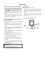
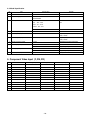
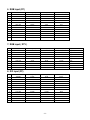
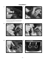
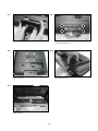
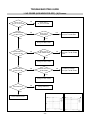
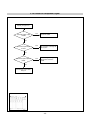
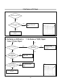
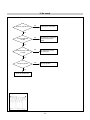
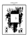
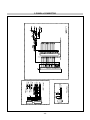
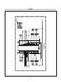
Website:http://biz.LGservice.com
E-mail:http://www.LGEservice.com/techsup.html
COLOR MONITOR
SERVICE MANUAL
CHASSIS NO. : LP69G
MODEL:
M208WA (M208WA-BZH.A**VLP)
*(
) **Same model for Service
CAUTION
BEFORE SERVICING THE UNIT,
READ THE SAFETY PRECAUTIONS IN THIS MANUAL.
CONTENTS
CONTENTS .............................................................................................. 2
PRECAUTION ...........................................................................................3
SPECIFICATION ........................................................................................7
DISASSEMBLY ........................................................................................13
ADJUSTMENT ........................................................................................15
SERVICE OSD .........................................................................................21
TROUBLE SHOOTING ............................................................................22
BLOCK DIAGRAM...................................................................................28
EXPLODED VIEW ...................................................................................31
REPLACEMENT PARTS LIST ............................................................... 33
SVC. SHEET ...............................................................................................
-2-
PRECAUTION
WARNING FOR THE SAFETY-RELATED COMPONENT.
WARNING
• There are some special components used in LCD
monitor that are important for safety. These parts are
marked on the schematic diagram and the
replacement parts list. It is essential that these critical
parts should be replaced with the manufacturer’s
specified parts to prevent electric shock, fire or other
hazard.
• Do not modify original design without obtaining written
permission from manufacturer or you will void the
original parts and labor guarantee.
BE CAREFUL ELECTRIC SHOCK !
• If you want to replace with the new backlight (CCFL) or
inverter circuit, must disconnect the AC adapter
because high voltage appears at inverter circuit about
650Vrms.
• Handle with care wires or connectors of the inverter
circuit. If the wires are pressed cause short and may
burn or take fire.
Leakage Current Hot Check Circuit
TAKE CARE DURING HANDLING THE LCD MODULE
WITH BACKLIGHT UNIT.
AC Volt-meter
• Must mount the module using mounting holes arranged
in four corners.
• Do not press on the panel, edge of the frame strongly
or electric shock as this will result in damage to the
screen.
• Do not scratch or press on the panel with any sharp
objects, such as pencil or pen as this may result in
damage to the panel.
• Protect the module from the ESD as it may damage the
electronic circuit (C-MOS).
• Make certain that treatment person’s body are
grounded through wrist band.
• Do not leave the module in high temperature and in
areas of high humidity for a long time.
• The module not be exposed to the direct sunlight.
• Avoid contact with water as it may a short circuit within
the module.
• If the surface of panel become dirty, please wipe it off
with a softmaterial. (Cleaning with a dirty or rough cloth
may damage the panel.)
CAUTION
Please use only a plastic screwdriver to protect yourself
from shock hazard during service operation.
-3-
Good Earth Ground
such as WATER PIPE,
CONDUIT etc.
To Instrument's
exposed
METALLIC PARTS
1.5 Kohm/10W
SERVICING PRECAUTIONS
CAUTION: Before servicing receivers covered by this
service manual and its supplements and addenda, read
and follow the SAFETY PRECAUTIONS on page 3 of this
publication.
NOTE: If unforeseen circumstances create conflict
between the following servicing precautions and any of the
safety precautions on page 3 of this publication, always
follow the safety precautions. Remember: Safety First.
General Servicing Precautions
1. Always unplug the receiver AC power cord from the AC
power source before;
a. Removing or reinstalling any component, circuit
board module or any other receiver assembly.
b. Disconnecting or reconnecting any receiver electrical
plug or other electrical connection.
c. Connecting a test substitute in parallel with an
electrolytic capacitor in the receiver.
CAUTION: A wrong part substitution or incorrect
polarity installation of electrolytic capacitors may
result in an explosion hazard.
d. Discharging the picture tube anode.
2. Test high voltage only by measuring it with an
appropriate high voltage meter or other voltage
measuring device (DVM, FETVOM, etc) equipped with
a suitable high voltage probe.
Do not test high voltage by "drawing an arc".
3. Discharge the picture tube anode only by (a) first
connecting one end of an insulated clip lead to the
degaussing or kine aquadag grounding system shield
at the point where the picture tube socket ground lead
is connected, and then (b) touch the other end of the
insulated clip lead to the picture tube anode button,
using an insulating handle to avoid personal contact
with high voltage.
4. Do not spray chemicals on or near this receiver or any
of its assemblies.
5. Unless specified otherwise in this service manual,
clean electrical contacts only by applying the following
mixture to the contacts with a pipe cleaner, cottontipped stick or comparable non-abrasive applicator;
10% (by volume) Acetone and 90% (by volume)
isopropyl alcohol (90%-99% strength)
CAUTION: This is a flammable mixture.
Unless specified otherwise in this service manual,
lubrication of contacts in not required.
6. Do not defeat any plug/socket B+ voltage interlocks
with which receivers covered by this service manual
might be equipped.
7. Do not apply AC power to this instrument and/or any of
its electrical assemblies unless all solid-state device
heat sinks are correctly installed.
8. Always connect the test receiver ground lead to the
receiver chassis ground before connecting the test
receiver positive lead.
Always remove the test receiver ground lead last.
9. Use with this receiver only the test fixtures specified in
this service manual.
CAUTION: Do not connect the test fixture ground strap
to any heat sink in this receiver.
Electrostatically Sensitive (ES) Devices
Some semiconductor (solid-state) devices can be
damaged easily by static electricity. Such components
commonly are called Electrostatically Sensitive (ES)
Devices. Examples of typical ES devices are integrated
circuits and some field-effect transistors and
semiconductor "chip" components. The following
techniques should be used to help reduce the incidence of
component damage caused by static by static electricity.
1. Immediately before handling any semiconductor
component or semiconductor-equipped assembly, drain
off any electrostatic charge on your body by touching a
known earth ground. Alternatively, obtain and wear a
commercially available discharging wrist strap device,
which should be removed to prevent potential shock
reasons prior to applying power to the unit under test.
2. After removing an electrical assembly equipped with
ES devices, place the assembly on a conductive
surface such as aluminum foil, to prevent electrostatic
charge buildup or exposure of the assembly.
3. Use only a grounded-tip soldering iron to solder or
unsolder ES devices.
4. Use only an anti-static type solder removal device.
Some solder removal devices not classified as "antistatic" can generate electrical charges sufficient to
damage ES devices.
5. Do not use freon-propelled chemicals. These can
generate electrical charges sufficient to damage ES
devices.
6. Do not remove a replacement ES device from its
protective package until immediately before you are
ready to install it. (Most replacement ES devices are
packaged with leads electrically shorted together by
conductive foam, aluminum foil or comparable
conductive material).
7. Immediately before removing the protective material
from the leads of a replacement ES device, touch the
protective material to the chassis or circuit assembly
into which the device will be installed.
CAUTION: Be sure no power is applied to the chassis
or circuit, and observe all other safety precautions.
8. Minimize bodily motions when handling unpackaged
replacement ES devices. (Otherwise harmless motion
such as the brushing together of your clothes fabric or
the lifting of your foot from a carpeted floor can
generate static electricity sufficient to damage an ES
device.)
-4-
General Soldering Guidelines
1. Use a grounded-tip, low-wattage soldering iron and
appropriate tip size and shape that will maintain tip
temperature within the range or 500 F to 600 F.
2. Use an appropriate gauge of RMA resin-core solder
composed of 60 parts tin/40 parts lead.
3. Keep the soldering iron tip clean and well tinned.
4. Thoroughly clean the surfaces to be soldered. Use a
mall wire-bristle (0.5 inch, or 1.25cm) brush with a
metal handle.
Do not use freon-propelled spray-on cleaners.
5. Use the following unsoldering technique
a. Allow the soldering iron tip to reach normal
temperature.
(500 F to 600 F)
b. Heat the component lead until the solder melts.
c. Quickly draw the melted solder with an anti-static,
suction-type solder removal device or with solder
braid.
CAUTION: Work quickly to avoid overheating the
circuitboard printed foil.
6. Use the following soldering technique.
a. Allow the soldering iron tip to reach a normal
temperature (500 F to 600 F)
b. First, hold the soldering iron tip and solder the strand
against the component lead until the solder melts.
c. Quickly move the soldering iron tip to the junction of
the component lead and the printed circuit foil, and
hold it there only until the solder flows onto and
around both the component lead and the foil.
CAUTION: Work quickly to avoid overheating the
circuit board printed foil.
d. Closely inspect the solder area and remove any
excess or splashed solder with a small wire-bristle
brush.
IC Remove/Replacement
Some chassis circuit boards have slotted holes (oblong)
through which the IC leads are inserted and then bent flat
against the circuit foil. When holes are the slotted type,
the following technique should be used to remove and
replace the IC. When working with boards using the
familiar round hole, use the standard technique as
outlined in paragraphs 5 and 6 above.
Removal
1. Desolder and straighten each IC lead in one operation
by gently prying up on the lead with the soldering iron
tip as the solder melts.
2. Draw away the melted solder with an anti-static
suction-type solder removal device (or with solder
braid) before removing the IC.
Replacement
1. Carefully insert the replacement IC in the circuit board.
2. Carefully bend each IC lead against the circuit foil pad
and solder it.
3. Clean the soldered areas with a small wire-bristle
brush. (It is not necessary to reapply acrylic coating to
the areas).
"Small-Signal" Discrete Transistor
Removal/Replacement
1. Remove the defective transistor by clipping its leads as
close as possible to the component body.
2. Bend into a "U" shape the end of each of three leads
remaining on the circuit board.
3. Bend into a "U" shape the replacement transistor leads.
4. Connect the replacement transistor leads to the
corresponding leads extending from the circuit board
and crimp the "U" with long nose pliers to insure metal
to metal contact then solder each connection.
Power Output, Transistor Device
Removal/Replacement
1. Heat and remove all solder from around the transistor
leads.
2. Remove the heat sink mounting screw (if so equipped).
3. Carefully remove the transistor from the heat sink of the
circuit board.
4. Insert new transistor in the circuit board.
5. Solder each transistor lead, and clip off excess lead.
6. Replace heat sink.
Diode Removal/Replacement
1. Remove defective diode by clipping its leads as close
as possible to diode body.
2. Bend the two remaining leads perpendicular y to the
circuit board.
3. Observing diode polarity, wrap each lead of the new
diode around the corresponding lead on the circuit
board.
4. Securely crimp each connection and solder it.
5. Inspect (on the circuit board copper side) the solder
joints of the two "original" leads. If they are not shiny,
reheat them and if necessary, apply additional solder.
Fuse and Conventional Resistor
Removal/Replacement
1. Clip each fuse or resistor lead at top of the circuit board
hollow stake.
2. Securely crimp the leads of replacement component
around notch at stake top.
3. Solder the connections.
CAUTION: Maintain original spacing between the
replaced component and adjacent components and the
circuit board to prevent excessive component
temperatures.
-5-
Circuit Board Foil Repair
Excessive heat applied to the copper foil of any printed
circuit board will weaken the adhesive that bonds the foil
to the circuit board causing the foil to separate from or
"lift-off" the board. The following guidelines and
procedures should be followed whenever this condition is
encountered.
At IC Connections
To repair a defective copper pattern at IC connections use
the following procedure to install a jumper wire on the
copper pattern side of the circuit board. (Use this
technique only on IC connections).
1. Carefully remove the damaged copper pattern with a
sharp knife. (Remove only as much copper as
absolutely necessary).
2. carefully scratch away the solder resist and acrylic
coating (if used) from the end of the remaining copper
pattern.
3. Bend a small "U" in one end of a small gauge jumper
wire and carefully crimp it around the IC pin. Solder the
IC connection.
4. Route the jumper wire along the path of the out-away
copper pattern and let it overlap the previously scraped
end of the good copper pattern. Solder the overlapped
area and clip off any excess jumper wire.
At Other Connections
Use the following technique to repair the defective copper
pattern at connections other than IC Pins. This technique
involves the installation of a jumper wire on the
component side of the circuit board.
1. Remove the defective copper pattern with a sharp
knife.
Remove at least 1/4 inch of copper, to ensure that a
hazardous condition will not exist if the jumper wire
opens.
2. Trace along the copper pattern from both sides of the
pattern break and locate the nearest component that is
directly connected to the affected copper pattern.
3. Connect insulated 20-gauge jumper wire from the lead
of the nearest component on one side of the pattern
break to the lead of the nearest component on the
other side.
Carefully crimp and solder the connections.
CAUTION: Be sure the insulated jumper wire is
dressed so the it does not touch components or sharp
edges.
-6-
SPECIFICATION
NOTE : Specifications and others are subject to change without notice for improvement.
1. Application range
3. Test method
This specification is applied to 20" Wide Monitor TV used
LP69G chassis.
2. Requirement for Test
Each part is tested as below without special appointment.
3.1 Performance : LGE test method followed
3.2 Demanded other specification
Safety : CE, IEC Specification
EMC : CE, IEC
(1) Power Voltage : Standard input voltage (100~240V@,
50/60Hz)
*Standard Voltage of each products is marked by models.
(2) Specification and performance of each parts are followed
each drawing and specification by part number in
accordance with BOM.
(3) The receiver must be operated for about 20 minutes prior
to the adjustment.
4. General Specification(TV)
4-1. General Specification
4.1.1 TV
No
Item
Specification
Remark
1
Video input applicable system
PAL-D/K, B/G, I, SECAM L, NTSC, NTSC 4.43
2
Receivable Broadcasting System
PAL/SECAM BG
(BZH/BTH)
PAL/SECAM DK
EU/Non-EU
PAL I
(PAL Market)
SECAM L/L’
3
RF Input Channel
VHF
: E2 ~ E12
UHF
: E21 ~ E69
PAL
CATV : S1 ~ S20
HYPER : S21~ S41
L/L’ : B, C, D
FRANCE
4
Input Voltage
100-240V~, 50Hz/60Hz
5
Market
EU
6
Tuning System
FVS 100 program
PAL, 200 PR.(Option)
FS
NTSC
7
Operating Environment
8
Storage Environment
Temp : -10°C ~ 60°C non condensing
9
Display
LCD Module
Temp : 10°C~ 35°C
Humidity : 20% ~ 80%
Humidity : 5%~90% non condensing
-7-
4.1.2 RGB/DVI
No.
Item
Specification
1
Supported Sync. Type
Separate Sync., Digital
2
Operating Frequency
Analog
3
Resolution
Remark
Horizontal
28 ~ 83kHz
Vertical
56 ~ 75 Hz
Digital
Horizontal
28 ~ 83kHz
Vertical
56 ~ 75 Hz
Analog
Max.
1680 x 1050 @ 60Hz
Recommend
1680 x 1050 @ 60Hz
Digital
Max.
1680 x 1050 @ 60Hz
Recommend
1680 x 1050 @ 60Hz
4
Input Voltage
Voltage :100 - 240 Vac, 50 or 60Hz
5
Inrush Current
Cold Start : 50 A
6
Operating Condition
Power S/W On
On mode
Hot : 120 A
Sync (H/V)
Video
LED
Wattage
On/On
Active
Blue
60W
Max.
On/On
Active
Blue
50W
Typ.
Off
Amber
1W
Off
Off
1W
Off/On
Sleep mode
Power S/W Off
On/Off
Off mode
-
7
MTBF
50,000 HRS with 90% Confidence level
8
Using Altitude
5,000 m (for Reliability) 3,000m(for FOS)
9
Operating Environment
Temp : 10°C ~ 35°C
10
Storage Environment
Lamp Life : 50,000 Hours(min)
Humidity : 20% ~ 80%
Temp : -10°C ~ 60°C non condensing
Humidity : 5% ~ 90% non condensing
4-2. Module Specification(AUO M201EW02-V1, P/N:EAJ33945701_ZBD, EAJ33945701_Non-ZBD)
No.
Item
Min
Typ.
1.
Type
TFT Color LCD Module
2.
Active Display area
433.44 (H) x 270.9 (V)
mm
3.
Outline dimension
459.4 (H) x 296.4 (V) x16.6 (D)
mm
4.
Pixel pitch
0.258mm (H) x 0.258mm (V) x RGB
mm
5.
Color arrangement
RGB vertical stripe
6.
Color Depth
16.7M color
7.
Electrical Interface
LVDS
8.
Surface Treatment
Hard coating(3H) & Anti-glare(Haze 25)
9.
Operating Mode
Normally White
10.
Back light Unit
4 CCFL (4 lamps)
11.
R/T
R.T : 3.6ms + R.T : 1.4ms
-8-
Max
Unit
Remark
Typ
Typ.
4-3. Optical characteristic specifications
4.3.1 Optical Characteristic
No.
Item
Specification
Min
1
Viewing Angle
2
Luminance
R/L
<CR≥10>
RGB-PC
(cd/m2)
AV1/AV2/TV
Component
White Luminance Uniformity
3
Contrast Ratio
CR
Typ
Max
80/80
U/D
Luminance
Remark
80/80
240
300
PSM:Dynamic, CSM: 6500K
190
230
PSM:Dynamic, CSM:Cool
75
80
RGB-PC/
AV1/AV2/TV/
At DFC Mode
1000
Typ. 3000:1, Min. 2400:1
Component
4
CIE Color Coordinates
WHITE
Wx
Wy
0.329
RED
Rx
0.640
Ry
Typ.
0.352
Typ.
PSM : Dynamic
GREEN
Gx
-0.03
0.288
+0.03
CSM : 6500K
BLUE
WHITE
RED
GREEN
BLUE
0.313
In RGB-PC input
Gy
0.628
White
Bx
0.147
(100 IRE)
By
0.070
Wx
0.285
Wy
0.293
Rx
In AV1/AV2/Component/TV input
0.640
Ry
Typ.
0.334
Typ.
Gx
-0.015
0.286
+0.015
PSM : Dynamic
CSM : Cool
Gy
0.599
White
Bx
0.154
(85 IRE)
By
0.077
-9-
4-4. Model Specification
No
Item
1.
Market
2.
Broadcasting system
Specification
Remark
EU
PAL BG/I/DK, SECAM-L/L’,
SECAM BG/DK
3
RF Input Channel
VHF
: E2 ~ E12
UHF
: E21 ~ E69
PAL
CATV : S1 ~ S20
HYPER : S21~ S41
L/L’ : B, C, D
FRANCE
4.
SCART Input (1EA)
PAL, SECAM
5.
CVBS Input (1EA)
PAL, SECAM, NTSC
6.
S-Video Input (1EA)
PAL, SECAM, NTSC
7.
Component Input (1EA)
Y/ Pb/Pr
8.
RGB Input (1EA)
4 System(Rear) :PAL50, SECAM,
NTSC, PAL60
4 System(Rear) : PAL50, SECAM,
NTSC, PAL60
9.
DVI Input (1EA)
10.
Audio Input (3 EA)
480i/480P/576i/576P/720P/1080i
RGB-PC
Max 1680 * 1050@60Hz
RGB-DTV
480p, 576p, 720p, 1080i
DVI-PC
Max 1680 * 1050@60Hz
DVI-DTV
480p, 576p, 720p, 1080i
CVBS, PC Audio, Component
L/R Input
5. Component Video Input (Y, PB, PR)
No
Resolution
H-freq(kHz)
V-freq.(kHz)
Pixel clock(MHz)
1.
720*480
15.73
59.94
13.500
Proposed
2.
720*480
15.75
60.00
13.514
480i
3.
720*576
15.625
50.00
13.500
576i
4.
720*480
31.47
59.94
27.000
480P
5.
720*480
31.50
60.00
27.027
480P
6.
720*576
31.25
50.00
27.000
576P
7.
1280*720
44.96
59.94
74.176
720P
8.
1280*720
45.00
60.00
74.250
720P
9.
1280*720
37.50
50.00
74.25
720P
10.
1920*1080
33.72
59.94
74.176
1080i
480i
11.
1920*1080
33.75
60.00
74.250
1080i
12.
1920*1080
28.125
50.00
74.250
1080i
- 10 -
6. RGB Input (PC)
No
Resolution
H-freq(kHz)
V-freq.(Hz)
Pixel clock(MHz)
1
720*400
31.468
70.08
28.321
2
640*480
31.469
59.94
25.175
3
640*480
37.5
75
31.5
4
800*600
37.879
60.317
40.0
5
800*600
46.875
75.0
49.5
6
1024*768
48.363
60.0
65.0
7
1024*768
60.123
75.029
78.75
8
1152*864
67.500
75.000
108.0
9
1280*1024
63.981
60.02
108.0
10
1280*1024
79.976
75.035
135.0
11
1680*1050
64.674
59.883
119.0
12
1680*1050
65.290
59.954
146.25
7. RGB input ( DTV )
No
Resolution
H-freq(kHz)
V-freq.(kHz)
Pixel clock(MHz)
1.
720*480
31.47
59.94
27.000
480p
2.
720*480
31.50
60.00
27.027
480p
3.
720*576
31.25
50.00
27.000
576p
4.
1280*720
37.5
50.00
74.250
720p
5.
1280*720
44.96
59.94
74.176
720p
6.
1280*720
45.00
60.00
74.250
720p
7.
1920*1080
33.72
59.94
74.176
1080i
8
1920*1080
33.75
60.00
74.250
1080i
9
1920*1080
28.125
50.00
74.250
1080i
8. DVI input (PC)
No
Resolution
H-freq(kHz)
V-freq.(Hz)
Pixel clock(MHz)
1
720*400
31.468
70.08
28.321
2
640*480
31.469
59.94
25.175
3
640*480
37.5
75
31.5
4
800*600
37.879
60.317
40.0
5
800*600
46.875
75.0
49.5
6
1024*768
48.363
60.0
65.0
7
1024*768
60.123
75.029
78.75
8
1152*864
67.500
75.000
108.0
9
1280*1024
63.981
60.02
108.0
10
1280*1024
79.976
75.035
135.0
11
1680*1050
64.674
59.883
119.0
12
1680*1050
65.290
59.954
146.25
- 11 -
Proposed
9. DVI input (DTV)
No
Resolution
H-freq(kHz)
V-freq.(kHz)
Pixel clock(MHz)
1.
720*480
31.47
59.94
27.000
480p
2.
720*480
31.50
60.00
27.027
480p
3.
720*576
31.25
50.00
27.000
576p
4.
1280*720
37.5
50.00
74.250
720p
5.
1280*720
44.96
59.94
74.176
720p
6.
1280*720
45.00
60.00
74.250
720p
7.
1920*1080
33.72
59.94
74.176
1080i
8.
1920*1080
33.75
60.00
74.250
1080i
9.
1920*1080
28.125
50.00
74.250
1080i
- 12 -
Proposed
DISASSEMBLY
#1
#2
Push the button.
1. Push down slightly to disassembly it.
2. After push the cable management like above fig.(Downward),
Disassembly the Cable management with pulling it upward.
3. Disassembly Cable Holder.
#4
#3
Hold the stand base.
#5
Disassembly stand base.
#6
Remove base body Like a picture.
Push 2 letches Like a picture.
- 13 -
#8
#7
Pull base body to separate from set during pressing 2 letches.
1. Remove the screws.
2. Disassembly Hinge Cover.
#9
# 10
Disassembly back cover.
Remove the screws.
# 11
Pull the connector.
- 14 -
ADJUSTMENT INSTRUCTION
1. Application Range
This specification sheet is applied to 19"/ 20"/ 22" LCD
Monitor TV which is manufactured in TV (or Monitor) Factory
or is produced on the basis of this data.
2. Specification
1) The adjustment is according to the order which is
designated and which must be followed, according to the
plan which can be changed only on agreeing.
2) Power Adjustment : Free Voltage
3) Magnetic Field Condition : Nil.
4) Input signal Unit : Product Specification Standard
5) Reserve after operation : Above 30 Minutes
6) Adjustment equipments : Color Analyzer(CA-210 or CA110), Pattern Generator (MSPG-925L or Equivalent), DDC
Adjustment Jig equipment, SVC remote controller
3. Main PCB check process
* APC - After Manual-Insult, executing APC
3.1. Download
1) Execute ISP program “Mstar ISP Utility” and then click
“Config” tab.
2) Set as below, and then click “Auto Detect” and check
“OK” message.
If display “Error”, Check connect computer, jig, and set.
3) Click “Connect” tab.
If display “Can’t ”, Check connect computer, jig, and set.
3.2. ADC Process
* If a scaler IC changed for PCB repairing, it is need to do
ADC process at all times.
(1) PC input ADC
1) Auto RGB Gain/Offset Adjustment
- Convert to PC in Input-source
- Signal equipment displays
Output Voltage : 700 mVp-p
Impress Resolution XGA (1024 x 768 @ 60Hz)
Model : 60 in Pattern Generator
Pattern : 29 in Pattern Generator (MSPG-925
SERISE)
[gray pattern that left & right is black and center is
white signal (Refer below picture)].
<Adjustment pattern (PC)>
4) Click “Read” tab, and then load download
file(XXXX.bin) by clicking “Read”.
- Adjust by commanding AUTO_COLOR _ADJUST
(0xF1) 0x00 0x02 instruction.
2) Confirmation
- We confirm whether “0x8B,0x8C” address of
EEPROM “0xB4” is “0xAA” or not.
- If “0x8B,0x8C” address of EEPROM “0xB4” isn’t
“0xAA”, we adjust once more.
- We can confirm the ADC values from “0x00~0x05”
addresses in a page “0xB4”
* Manual ADC process using Service Remocon. After
enter Service Mode by pushing “INSTART” key,
execute “Auto-RGB” by pushing “_” key at “AutoRGB”.
(2) COMPONENT input ADC
1) Component Gain/Offset Adjustment
- Convert to Component in Input-source
- Signal equipment displays
Impress Resolution 480P
MODEL : 212 in Pattern Generator
(480p Mode, Y : 100%, Pb/Pr : 75%)
PATTERN : 08 in Pattern Generator
(MSPG-925 SERISE)
5) Click “Auto” tab and set as below
6) click “Run”.
7) After downloading, check “OK” message.
- 15 -
4.3. Confirm color coordinate of AV2
(1) Set Input to AV2
(2) Input signal : CVBS, PAL @ 50Hz
Full white 216/255 gray level (85 IRE, Model : 202,
Pattern : 78 at MSPG925L)
(3) Set PSM : Dynamic / CSM : Cool
(4) Confirm whether x = 0.285±0.03, y = 0.293±0.03 or
not.
<Adjustment pattern (COMPONENT)>
- Adjust by commanding AUTO_COLOR_ADJUST
(0xF1) 0x00 0x02 instruction.
2) Confirmation
- We confirm whether “0x8D,0x8E” address of
EEPROM “0xB4” is “0xAA” or not.
- If “0x8D,0x8E” address of EEPROM “0xB4” isn’t
“0xAA”, we adjust once more.
- We can confirm the ADC values from “0x00~0x05”
addresses in a page “0xB4”.
3.3. Function Check
(1) Check display and sound
- Check Input and Signal items. ( cf. work instructions)
1) TV
2) AV1 (SCART)
3) AV2 (CVBS/ S-Video)
4) COMPONENT (480P)
5) RGB (PC : 1024 x 768 @ 60hz)
6) DVI
7) PC Audio In and H/P Out
* Display and Sound check is executed by Remote
controller.
4. Total Assembly line process
4.1. Adjustment Preparation
(1) Above 30 minutes H/run in RF no signal
(2) 15 Pin D-Sub Jack is connected to the signal of Pattern
Generator.
4.2. Confirm color coordinate of RGB
* Check White Balance
- Set Input to RGB.
- Input signal : (1024 x 768 @ 60Hz), Full white 255/255
gray level (100 IRE, Model : 60, Pattern : 4
at MSPG925L)
- Set CSM : 6500k
- Confirm whether x = 0.313±0.03, y = 0.329±0.03 or not.
- Confirm whether luminance over 200cd/m2
- Set CSM : 9300k
- Confirm whether x = 0.283±0.03, y = 0.298±0.03 or not.
* Check sRGB
- Set Input to RGB.
- Input signal : (1024 x 768 @ 60Hz)
Full white 255/255 gray level (100 IRE, Model : 60,
Pattern : 4 at MSPG925L)
- Set CSM : sRGB
- Confirm whether x = 0.313±0.03, y = 0.329±0.03 or not.
- Confirm whether luminance = 180±50 cd/m2
- 16 -
4.4. Confirm color coordinate of component
(1) Set Input to COMPONENT.
(2) Input signal : 480P
Full white 216/255 gray level (85 IRE Model : 212,
Pattern : 78 at MSPG925L)
(3) Set PSM : Dynamic / CSM : Cool
(4) Confirm whether x = 0.285±0.03, y = 0.293±0.03 or
not.
4.5. Confirm Auto adjustment operation.
(1) Input 1 Dot on/off & Rectangle Pattern at Model 60
(1024 x 768@60Hz).
(2) Confirm adjustment operation by changing Clock,
Phase, H/V Position.
(3) Check Clock, Phase by pressing AUTO Key after
varying the Clock & the Phase
4.6. Other quality
- Confirm that each items satisfy under standard
condition that was written product spec.
(1) AV
1) Select input AV1 and whether picture is displayed or
not. - SCART output displayed or not.
2) Select input AV2 (S-video) and whether picture is
displayed or not
3) Select input AV2 (CVBS) and whether picture is
displayed or not.
(2) TV
- Select input TV and check below item
* In Gumi Factory
C05 (E05) – TELETEXT Function Check
; (Applicable to the model that has Teletext code set-up
item in Product spec)
C07 (E07) – Nicam DUAL Check.
C52 (E52) – Nicam Stereo Check.
Refer to “7.Preset CH information”.
(3) RGB
*M198WA
- Select input RGB model 112(1440*900@60hz), 64 Gray
Scale pattern and whether picture is displayed or not
*M208WA / M228WA
- Select input RGB model 122(1680*1050@60hz), 64Gray
Scale pattern and whether picture is display or not
(4) COMPONENT
- Select input COMPONENT and whether picture is
displayed or not.
2) DIGITAL DATA 256Byte
(5) DVI
*M198WA
- Select input DVI model 112(1440*900@60hz), 64 Gray
Scale pattern and whether picture is displayed or not
*M208WA / M228WA
- Select input DVI model 122(1680*1050@60hz), 64Gray
pattern and whether picture is displayed or not.
4.7. DPM operation confirmation
- Check if Power LED Color and Power Consumption operate
as standard.
(1) Set Input to RGB and connect D-sub cable to set.
(2) Measurement Condition : 230V@ 50Hz (Analog)
(3) Confirm DPM operation at the state of screen without
Signal
(3) M228WA EDID DATA
1) ANALOG DATA 128Byte
4.8 DDC EDID Write
1) Connect D-sub Signal Cable to D-Sub Jack.
2) Connect HDMI Signal Cable to HDMI Jack.
3) Write EDID DATA to EEPROM(24C02) by using DDC2B
protocol.
4) Check whether written EDID data is correct or not. (refer
to Product spec).
2) DIGITAL DATA 256Byte
(1) M198WA EDID DATA
1) ANALOG DATA 128Byte
4.9. HDCP SETTING
(High-Bandwidth Digital Contents Protection)
2) DIGITAL DATA 256Byte
1) Connect D-sub Signal Cable to D-Sub Jack.
2) Input HDCP key with HDCP-key- in-program.
3) HDCP Key value is stored on EEPROM(AT24C64)
which is E00~F20 addresses of 0xBC~0xBE page.
(2) M208WA EDID DATA
ADH
ADL
LEN
BC
00
128
BC
80
128
BE
00
33
1) ANALOG DATA 128Byte
4) AC off/ on and on HDCP button of MSPG925 and
confirm whether picture is displayed or not of using
MSPG925.
5) HDCP Key value is different among the sets.
4.10. Outgoing condition Configuration
1) After all function test., press IN-STOP Key by SVC
Remote controller. And Make Ship Condition.
2) When pressing IN-STOP key by SVC remocon, Green
and red LED are blinked alternatively. And then
Automatically turn off. (Must not AC power OFF during
blinking)
- 17 -
4.11. Internal pressure
- Confirm whether is nomal or not when between power
board's ac block and GND is impacked on 1.5kV(dc) or
2.2kV(dc) for one second.
Option 4(3)
1
Default Lang (Language)
3
2
Lang
0
Chesky,Dansk,Deutsch,English
Español,Français,Italiano,
4.12 Option data setting (SVC OSD setting)
Magyar,Nederlands,Norsk,
Polski,Português,
(1) PAL Model
Romaneste,Suomi,Svenska
*M198WA(Change by Suffix) Tool Option 8065
M198WA-BZH
Resolution
1
Module
0
TV
1
SCART
1
AV2
1
COMPONENT
1
PC-RGB
1
DVI
1
HDMI
0
3
REMARK
T- Lang
0
AUSTRIA,BULGARIA,
CROATIA,CZECH, DENMARK,
WXGA+
ESTONIA,FINLAND,FRANCE,
GERMANY,GREECE,
HUNGARY,ITALY,LATVIA,
NETHERLANDS,NORWAY,
POLAND,PORTUGAL,
RUMANIA,RUSSIA,SERBIA,
SLOVAKIA,SLOVENIA,SPAIN,
SWEDEN,SWITZERLAND,
TURKEY,UK,ARAB,HEBREW,
Others
*M208WA/M228WA(Change by Suffix) Tool Option 8066
M208WA-BZH / M228WA-BZH
REMARK
2
WSXGA
Resolution
Module
0
TV
1
SCART
1
AV2
1
COMPONENT
1
PC-RGB
1
DVI
1
HDMI
0
Option5(9)
1
Item
Condition
200PR
0
2
ACMS
1
Remark
1
0 : 200 PR Off
0 : ACMS Off
TOP
FLOF
4
CH+AU
0
5
BOOSTER
0
1
SYS
0
2
A2 ST
1
0 : Except below area
1 : China, Australia
0 : BG/I/DK/L
1 : BG/I/DK/M
Acting FM-ST after checking
Nicam
I II SAVE
0
0 : I II SAVE Off
1 : I II SAVE On
4
HDEV
0
0 : Except below area
1 : China
5
V-Curve
0
0 : Turbo Volume Off
1 : Turbo Volume On
6
MONO
0
Option3(2)
1
KEY-TYPE
2
FACTORY-MODE 0
0
4
CHANNEL-MUTE 1
1
Clock Phase
7
2
DQS0 Phase
2
3
DQS1 Phase
2
4
DQS2 Phase
2
5
DQS3 Phase
2
1
Last Power
0
2
Remocon
0
3
Key
0
4
Sleep Timer
0
5
RS232
0
6
Off Timer
0
7
Auto Off
0
8
2Hour Off
0
9
Reset
0
ETC
Option2(2)
3
TV-LINK-TUNER
3
0 : EEPROM Write Protection On
Power Off History
1 : ACMS On
Text
2
Ram Delay
1 : 200 PR On
3
0 : 2 Hour off option -OFF
1 : EEPROM Write Protection Off
Option1(6)
1
1
1 : 2 Hour off option -ON
*M198WA/M208WA/M228WA(Change by Suffix) Area Option 00
No.
2HR-OFF
2 : 8Key
- 18 -
1
DFC Control
1
2
Exit Key
0
3
PWM DIM
255
4
Dimming Ctl.
255
5
DEBUG ON
0
6
UART ON
3
7
AGC AKEOVER
16
8
AGC EData
0
9
AGC BData
0
10
VID Lev
96
(2) Command Set
5. Adjustment Command
5.1. Adjustment Commands(LENGTH=84)
Adjustment Contents
FACTORY ON
CMD
ADR
(hex)
E0
00
VAL
00
Adjustment contents CMD(hex) ADH(hex) ADL(hex)
EEPROM READ
Description
E7
A0
Factory mode on
FACTORY OFF
E2
00
00
Factory mode off
EEPROM ALL INIT.
E4
00
00
EEPROM All clear
EEPROM Read
E7
00
00
EEPROM Read
EEPROM Write
E8
00
data
0
80
0-Page 80~FF Read
0
1-Page 0~7F Read
A2
80
1-Page 80~FF Read
0
2-Page 0~7F Read
A4
EEPROM Write by some
80
2-Page 80~FF Read
0
3-Page 0~7F Read
80
3-Page 80~FF Read
A6
values
Details
0-Page 0~7F Read
COLOR SAVE
(R/G/B cutoff, Drive,
EB
00
00
Color Save
* Purpose : To read the appointment Address of
E2PROM by 128(80h)-byte
Contrast, Bright)
H POSITION
20
00
00 – 100 They have different range
V POSITION
30
00
00 – 100 each mode, FOS Adjustment
CLOCK
90
00
00 – 100
5.3. E2PROM Data Write
(1) Signal Table
PHASE
92
00
00 – 100
R DRIVE
16
00
00 – FF
G DRIVE
18
00
00 – FF
B DRIVE
1A
00
00 – FF
R CUTOFF
80
00
00 – 7F
G CUTOFF
82
00
00 – 7F
B CUTOFF
84
00
00 – 7F
BRIGHT
10
00
00 – 3F
Bright adjustment
CONTRAST
12
00
00 - 64
Luminance adjustment
AUTO_COLOR_
F1
00
02
F2
00
0,1,2,3
Drive adjustment
LEN : 84h+Bytes
CMD : 8Eh
ADH : E2PROM Slave Address(A0,A2,A4,A6,A8), Not
00h(Reserved by BufferToEEPROM)
ADL : E2PROM Sub Address(00~FF)
Data : Write data
Offset adjustment
Auto COLOR Adjustment
(2) Command Set
ADJUST
CHANGE_COLOR
_TEMP
0: COOL
Adjustment contents
1: NORMAL
EEPROM WRITE
CMD(hex)
ADH(hex)
E8
94
2: WARM
84+n
3: USER
FACTORY_DEFAULT
F3
00
00
& Input change to “ TV”
F4
00
0,1,2,4
CHANGE
n-byte Write
* Purpose
1) EDID write : 16-byte by 16-byte, 8 order (128-byte)
write(TO “00 – 7F” of “EEPROM Page A4”).
2) FOS Default write : 16-mode data (HFh, HFl, VF, STD,
HP, VP, Clk, ClkPh, PhFine) write.
3) Random Data write : write the appointment Address of
E2PROM.
Factory mode off
& II_SW is “1”
AUTO_INPUT
Details
16-Byte Write
0 : TV
1 : AV1
2 : AV2
3 : Component
5.4. VRAM Read
4 : RGB
1) Send CMD(70h) to read Video RAM value from MICOM
And save its value to 128-Bytes Buffer(Common Buffer
for the use of EDID)
5 : DVI
5.2 EEPROM DATA READ
(1) Signal Table
2) Delay 500ms ( Time to Wait and Read Video RAM from
MICOM)
Delay 100ms
128 Bytes
3) Be transmitted the contents of MICOM’s 128-bytes
Buffer to PC. (128th Data is the CheckSum of 127-bytes
data : That’s OK if the value of adding 128-bytes Data is
Zero)
- 19 -
Windows EDID V1.0 User Manual
2. EDID Read & Write
1) Run WinEDID.exe
Operating System: MS Windows 98, 2000, XP
Port Setup: Windows 98 => Don’t need setup
Windows 2000, XP => Need to Port Setup.
This program is available to LCD Monitor only.
1. Port Setup
a) Copy “UserPort.sys” file to
“c:\WINNT\system32\drivers” folder
b) Run Userport.exe
2) Edit Week of Manufacture, Year of Manufacture,
Serial Number
a) Input User Info Data
b) Click “Update” button
c) Click “ Write” button
c) Remove all default number
d) Add 300-3FF
e) Click Start button.
f) Click Exit button.
- 20 -
SERVICE OSD
Description of operation
BLUEBIRD3 - LP69G
- Tool Option : Adjust Tool Option
- Area Option : Adjust Area Option
- Option 1 : Adjust Tuner Service Option
- Option 2 : Adjust Sound Service Option
- Option 3 : Adjust Local key
- Option 4 : Select default language
- Option 5 : Adjust ETC
- RAM Delay : Adjust RAM Delay
- Power Off History : Adjust Power Off History
- ETC
Version
2.01 061227
M208WA WSXGA AUO-20W
UTT
0
Tool Option
8066
Area Option
00
OPTION 1
6
OPTION 2
2
OPTION 3
2
OPTION 4
3
OPTION 5
9
RAM Delay
Power Off History
ETC
A
9
IBM
Compatible PC
Video Signal
Generator
15
10
5
11
6
1
6
1
5
C
d
PARALLEL PORT
tu
No
RS
23
2C
se
13
PA
RA
LL
EL
14
ON
F
Power inlet (required)
5V
PO
WE
R
220
VG
S
A
MO
NI
TO
R
V-S
YN
CS
T
Control Line
5V
C
1
25
OFF
Power Select Switch
(110V/220V)
Power LED
ON
4.7K
OFF
74LS06
B
E ST Switch
B
F V-Sync On/Off Switch
(Switch must be ON.)
Figure 1. Cable Connection
- 21 -
4.7K
4.7K
5V
E
74LS06
TROUBLESHOOTING GUIDE
1. NO POWER (LED INDICATOR OFF) : [A] Process
Check 15V or
ST_5V of Power B/D.
Fail
Check 15V or
ST_5V of Power B/D.
Fail
Check short of
IC100, Q307.
Pass
Check Output of
IC1100, IC1101.
Fail
Re-soldering of Change
defect part of IC100, Q307.
Fail
Re-soldering of Change
defect part of IC100, TU600,
IC500.
Fail
Re-soldering of Change
defect part of IC100, IC400.
Pass
Pass
Change IC1100, IC1101.
Check Output of
IC1102, IC1103.
Fail
Check short of
IC100, TU600, IC500.
Pass
Pass
Change IC1102, IC1103.
Check Output of
IC1104, IC1105.
Fail
Check short of
IC100, IC400.
Pass
Pass
Change IC1104, IC1105.
Check LED Assy.
Fail
Change LED Assy.
Pass
5V
Check P304 Connector.
- 22 -
15V
2. NO RASTER : [B] Process
Check LED status
On Display Unit.
Fail
Repeat A PROCESS.
Pass
Check Panel Link Cable
or Module.
Fail
Change Panel Link Cable
or Module.
Fail
Change Inverter Connector
or Inverter.
Pass
Check Inverter
Connector or inverter.
Pass
Check Output
of R305
Fail
Change R305
Pass
Check the LVDS Output
of IC100
Fail
Change IC100
Pass
Check Input source Cable
and Jack.
Fail
Change Module.
- 23 -
3. NO RASTER ON RGB SINGAL
Repeat [A, B] process.
Pass
Check the input/ output
of R708, R709
Fail
Check the J701.
Pass
Check
the input/output
of R128, R131, R136.
Fail
Re-soldering or Change the
defect part.
Fail
Re-soldering or change the
defect part, Check the
X100.
Pass
Check the input/output of
IC100.
Pass
Check input source cable
and jack.
X100
- 24 -
4. No Raster on Component Signal
Repeat [A, B] process.
Check the input/ output
of R901.
Fail
Check the J900.
Pass
Check the input/output
of R125.
Fail
Re-soldering or Change the
defect part.
Fail
Re-soldering or change the
defect part, Check the
X100.
Pass
Check the input/output of
IC100.
Pass
Check input source cable
and jack.
X100
- 25 -
5. No Raster on DVI Signal
Repeat [A, B] process.
Pass
Check the input/ output
of R100.
Fail
Re-soldering or change the
defect part, Check the
X100.
X100
Pass
Check input source cable
and jack.
6. No Raster on AV(Scart in
Video, S-Video) Signal
7. No Rasteron TV(RF) Signal
Pass
Pass
Fail
Repeat [A, B] process.
Check short of
IC100, Q307.
Fail
Check 5V of TU600.
Re-Soldering or change the
defect part.
Pass
Pass
Check
the input/output of
L804, L1002,L1003,
L1004.
Fail
Change L804, L1002,
L1003, L1004.
Fail
Re-soldering of Change
defect part, Check the
X100.
Pass
Check Output of
IC1104, IC1105.
Pass
Check input source cable
and jack.
- 26 -
X100
8. No sound
Fail
Check the input Sourse.
Change the source input.
Pass
Check input/Output
ofIC100.
Fail
Re-soldering of Change the
defect part, Check the
X100
Fail
Re-soldering of Change
the defect part.
Pass
Check the input/ output
of IC500
Pass
Fail
Check the Speaker
Change Speaker.
Pass
Check the Speaker wire.
X100
- 27 -
EEPROM
TMDS Signal
- 28 -
Tuner
TAFT-W005D
Y/Pb/Pr
SIF
CVBS
CVBS
Y/C
L/R
L/R
L/R
COMP Audio
CVBS Audio
PC Audio
CS4351
(DAC)
R/G/B/CVBS/Audio
CVBS/Audio
SCART
COMP
D-SUB Analog Signal (R/G/B/H/V)
DVI-D
EEPROM
MENU
OK
(LGE9789AD-LF)
Decorder
Scaler+Video
INPUT
POWER
IR
16Mb
SDRAM
(HY57V161610FTP)
PR
EEPROM
System(64k)
(YDA138)
Audio
Amp
(MX25L4005A)
4Mb
Serial
Flash
Memory
LVDS Signal
R
L
Data
(OCMD 0 ..7)
(OCMA 0 ..19)
Data
(FSD 0 . 31)
(FSA 0 ..11)
EAGLE EYE
VOL
SP (R)
SP (L)
(AUO)
LCD
Module
BLOCK DIAGRAM
DESCRIPTION OF BLOCK DIAGRAM
1. Power Supply Block (LIPS)
This Block Generates DC Voltage (5V,15V) to Main Control system from AC Power (100-240 V, 50/60 Hz, 1.0A)
2. DC/DC Converter block
DC/DC Converter convert the input 5V,15V to proper 1.8V,2.5V,3.3V,5V,10.5V for Main control system.
For shooting heat trouble, we use the DC/DC converting IC
3. Scaler + Video/Audio decorder (Scaler IC, LGE9789AD-LF)
It is composed of LGE9789AD-LF.
It includes AD Converter, LVDS/TMDS Transmitter, Micom, and Audio processor.
1) Video Signal - CVBS/S-Video/Component/RGB/DVI(TMDS)
This Block Selects input Video signals (like CVBS, Y/C, SCART RGB) and output RGB signal.
On decoding, We can control signal like Contrast, Brightness, Sharpness, Color, tint signals including Adaptive
Comb Filter.
2) Audio Signal
This block analyzes audio input signal through A/V Jack and PC audio and Tuner IF.
The analyzed signals transmitted to audio amplifier (YDA138)
On decoding, We can control signal like Bass, treble.
4. Flash Memory(MX25L4005A)
This is composed of MX25L4005A.
This store the source data of micom.
5. Tuner
Micom controls this IC through IIC line.
Tuner makes CVBS and transmits IF signal to LGE9789AD-LF.
6. Audio Amplifier (YDA138)
This block is composed of YDA138 and peripheral device.
The function of the audio amplifier is that to amplify audio L / R signal transmitted from audio decoder.
The audio signal is amplified according to pre-defined DC volume control curve.
Also, headphone amplifier is included at this IC.
- 29 -
LIPS Board Block Diagram
15V
50 ~ 60Hz
LINE
100 ~ 240V
EMI
COMPONENTS
INPUT RECTIFIER
AND FILTER
HVDC
ENERGY
TRANSFER
100KHz
OUTPUT RECTIFIER
AND FILTER
5V
GND
PWM
CONTROL
CIRCUIT
PHOTO
-COUPLER
ISOLATION
PRIMARY
SIGNAL
COLLENTION
SECONDARY
Operation description_LIPS
1. EMI components.
This part contains of EMI components to comply with global marketing EMI standards like FCC,VCCI CISPR, the
circuit included a line-filter, across line capacitor and of course the primary protection fuse.
2. Input rectifier and filter.
This part function is for transfer the input AC voltage to a DC voltage through a bridge rectifier and a bulk capacitor.
3. Energy Transfer.
This part function is for transfer the primary energy to secondary through a power transformer.
4. Output rectifier and filter.
This part function is to make a pulse width modulation control and to provide the driver signal to power switch, to
adjust the duty cycle during different AC input and output loading condition to achieve the dcoutput stabilized, and also
the over power protection is also monitor by this part.
5. Photo-Coupler isolation.
This part function is to feed back the DC output changing status through a photo transistor to primary controller to
achieve the stabilized DC output voltage.
6. Signal collection.
This part function is to collect the any change from the DC output and feed back to the primary through photo
transistor.
- 30 -
- 31 -
320
310
330
500
300
120
510
200
430
520
420
410
530
950
400
900
910
920
940
930
EXPLODED VIEW
PRINTED CIRCUIT BOARD
MAIN (TOP)
- 41 -
MAIN (BOTTOM)
- 42 -
CONTROL KEY
LED & P/SW
- 43 -
SCHEMATIC DIAGRAM
1. MSTAR
- 44 -
2. PANEL & CONNECTOR
- 45 -
3. DDR
- 46 -
4. AMP
- 47 -
5. TUNER
- 48 -
6. DSUB & DVI
- 49 -
7. SCART & DAC
- 50 -
8. JACK
- 51 -
9. POWER
- 52 -
10. CONTROL KEY
- 53 -
11. IR + LED + POWER
- 54 -
P/NO : MFL36713673
Jan. 2007
Printed in Korea