1
Advance Information
This document contains information on a product under development. The parametric information contains target parameters
that are subject to change.
Bt835 VideoStream III Decoder
Video Capture Processor and Scaler for TV/VCR Analog Input
The Bt835 VideoStream™ III Decoder is a high quality single-chip, composite
NTSC/PAL/SECAM video and S-Video decoder. Low operating power
consumption and power-down capability make it an ideal low-cost solution for
PC video capture applications on both desktop and portable system platforms.
The Bt835 supports square pixel and CCIR601 resolutions for NTSC, PAL and
SECAM video. The Bt835 has a sophisticated 3-line adaptive comb filter that
maintains full vertical video resolution and eliminates traditional comb filter
artifacts. The Bt835’s flexible pixel ports support digital video input as well as
VIP, VMI and ByteStream interfaces to popular graphics controllers.
XT0
Ultralock™
and
Clock
Generation
MUX3
REFP
AGC
40 MHz
ADC
CIN
40 MHz
ADC
Decimation LPF
AGCCAP
3-line Adaptive
Luma-Chroma
Separation
and
Chroma
Demodulation
Digital Input Video
Clock and Timing
I2C
JTAG
Video
Timing
Video
Timing
Unit
Spatial and
Temporal
Scaling
Digital Video
Input Data
Output Formatting
MUX2
•
•
•
•
MUX0
Analog
Video
MUX
•
•
•
Functional Block Diagram
MUX1
Distinguishing Features
•
•
•
Output
Control
16
Digital
Video
Output
Data
•
•
•
•
•
•
•
•
•
•
•
•
•
Single-chip composite/S-Video NTSC/PAL/
SECAM to YCrCb digitizer
On-chip Ultralock
Square pixel and CCIR601 resolution for:
– NTSC (M), NTSC (4.43)
– NTSC (M) without 7.5IRE pedestal
– PAL (B, D, G, H, I, M, N, N combination),
PAL (60)
– SECAM
NTSC 3-line adaptive comb filter
Arbitrary horizontal and 5-tap vertical filtered
scaling
Hardware closed-caption decoder
Vertical Blanking Interval (VBI) data
pass-through
Single crystal for any video format
Arbitrary temporal decimation for a reduced
frame-rate video sequence
Programmable hue, brightness, saturation,
and contrast
Digital video input port
2x oversampling to simplify external
analog filtering
Two-wire Inter-Integrated Circuit (I2C) bus
interface
8- or 16-bit pixel interface
YCrCb (4:2:2) output format
Software selectable four-input analog MUX
Eight fully programmable GPIO bits
Auto NTSC/PAL format detect
Automatic Gain Control (AGC)
Typical power consumption 500 mW (3.3 V)
IEEE 1149.1 Joint Test Action Group (JTAG)
interface
100-pin PQFP package
VIP, VMI, ByteStream interfaces
Related Products
•
Bt829B, Bt868/869
Applications
•
•
•
•
•
Multimedia
Image processing
Desktop video
Video phone
Interactive video
Ordering Information
Model Number
Package
Operating Temperature
Bt835KRF
100-pin PQFP
0°C to +70°C
Copyright © 1998 Rockwell Semiconductor Systems, Inc. All rights reserved.
Print date: October 1998
Rockwell Semiconductor Systems, Inc. reserves the right to make changes to its products or specifications to improve
performance, reliability, or manufacturability. Information furnished is believed to be accurate and reliable. However, no
responsibility is assumed for its use; nor for any infringement of patents or other rights of third parties which may result from its
use. No license is granted by its implication or otherwise under any patent or intellectual property rights of Rockwell
Semiconductor Systems, Inc.
Rockwell Semiconductor Systems, Inc. products are not designed or intended for use in life support appliances, devices, or systems
where malfunction of a Rockwell Semiconductor Systems, Inc. product can reasonably be expected to result in personal injury or
death. Rockwell Semiconductor Systems, Inc. customers using or selling Rockwell Semiconductor Systems, Inc. products for use
in such applications do so at their own risk and agree to fully indemnify Rockwell Semiconductor Systems, Inc. for any damages
resulting from such improper use or sale.
Bt is a registered trademark of Rockwell Semiconductor Systems, Inc.
Product names or services listed in this publication are for identification purposes only, and may be trademarks or registered
trademarks of their respective companies. All other marks mentioned herein are the property of their respective holders.
Specifications are subject to change without notice.
PRINTED IN THE UNITED STATES OF AMERICA
Table of Contents
List of Figures . . . . . . . . . . . . . . . . . . . . . . . . . . . . . . . . . . . . . . . . . . . . . . . . . . . . . . . . . . . . . . . . . . vii
List of Tables. . . . . . . . . . . . . . . . . . . . . . . . . . . . . . . . . . . . . . . . . . . . . . . . . . . . . . . . . . . . . . . . . . . . ix
1.0
Functional Description . . . . . . . . . . . . . . . . . . . . . . . . . . . . . . . . . . . . . . . . . . . . . . . . . . . . . . . . . . . 1
1.1
Functional Overview . . . . . . . . . . . . . . . . . . . . . . . . . . . . . . . . . . . . . . . . . . . . . . . . . . . . . . . . . . . 1
1.1.1
1.1.2
1.1.3
1.1.4
1.1.5
1.1.6
1.1.7
1.1.8
1.1.9
1.1.10
1.1.11
Bt835 Video Capture Processor for TV/VCR Analog Input. . . . . . . . . . . . . . . . . . . . . . . . . . .
Bt835 Architecture and Partitioning. . . . . . . . . . . . . . . . . . . . . . . . . . . . . . . . . . . . . . . . . . . .
Comb Filter . . . . . . . . . . . . . . . . . . . . . . . . . . . . . . . . . . . . . . . . . . . . . . . . . . . . . . . . . . . . . .
UltraLock . . . . . . . . . . . . . . . . . . . . . . . . . . . . . . . . . . . . . . . . . . . . . . . . . . . . . . . . . . . . . . . .
Scaling and Cropping . . . . . . . . . . . . . . . . . . . . . . . . . . . . . . . . . . . . . . . . . . . . . . . . . . . . . .
Input Interfaces . . . . . . . . . . . . . . . . . . . . . . . . . . . . . . . . . . . . . . . . . . . . . . . . . . . . . . . . . . .
Output Interface. . . . . . . . . . . . . . . . . . . . . . . . . . . . . . . . . . . . . . . . . . . . . . . . . . . . . . . . . . .
VBI Data Pass-through . . . . . . . . . . . . . . . . . . . . . . . . . . . . . . . . . . . . . . . . . . . . . . . . . . . . .
Closed Caption Decoding. . . . . . . . . . . . . . . . . . . . . . . . . . . . . . . . . . . . . . . . . . . . . . . . . . . .
I2C Interface . . . . . . . . . . . . . . . . . . . . . . . . . . . . . . . . . . . . . . . . . . . . . . . . . . . . . . . . . . . . .
3.3 V/5 V Operation . . . . . . . . . . . . . . . . . . . . . . . . . . . . . . . . . . . . . . . . . . . . . . . . . . . . . . . .
3
3
4
5
5
6
6
7
7
7
7
1.2
Pin Descriptions . . . . . . . . . . . . . . . . . . . . . . . . . . . . . . . . . . . . . . . . . . . . . . . . . . . . . . . . . . . . . . 8
1.3
UltraLock . . . . . . . . . . . . . . . . . . . . . . . . . . . . . . . . . . . . . . . . . . . . . . . . . . . . . . . . . . . . . . . . . . 11
1.3.1
1.3.2
The Challenge . . . . . . . . . . . . . . . . . . . . . . . . . . . . . . . . . . . . . . . . . . . . . . . . . . . . . . . . . . . 11
Operation Principles of UltraLock . . . . . . . . . . . . . . . . . . . . . . . . . . . . . . . . . . . . . . . . . . . . 11
1.4
Composite Video Input Formats . . . . . . . . . . . . . . . . . . . . . . . . . . . . . . . . . . . . . . . . . . . . . . . . . 13
1.5
Y/C Separation and Chroma Demodulation . . . . . . . . . . . . . . . . . . . . . . . . . . . . . . . . . . . . . . . . . 15
1.6
Video Scaling, Cropping, and Temporal Decimation . . . . . . . . . . . . . . . . . . . . . . . . . . . . . . . . . . 18
1.6.1
1.6.2
1.6.3
1.6.4
1.6.5
1.6.6
1.6.7
1.6.8
Horizontal and Vertical Scaling . . . . . . . . . . . . . . . . . . . . . . . . . . . . . . . . . . . . . . . . . . . . . .
Luminance Scaling . . . . . . . . . . . . . . . . . . . . . . . . . . . . . . . . . . . . . . . . . . . . . . . . . . . . . . .
Peaking . . . . . . . . . . . . . . . . . . . . . . . . . . . . . . . . . . . . . . . . . . . . . . . . . . . . . . . . . . . . . . . .
Chrominance Scaling. . . . . . . . . . . . . . . . . . . . . . . . . . . . . . . . . . . . . . . . . . . . . . . . . . . . . .
Scaling Registers. . . . . . . . . . . . . . . . . . . . . . . . . . . . . . . . . . . . . . . . . . . . . . . . . . . . . . . . .
Image Cropping. . . . . . . . . . . . . . . . . . . . . . . . . . . . . . . . . . . . . . . . . . . . . . . . . . . . . . . . . .
Cropping Registers . . . . . . . . . . . . . . . . . . . . . . . . . . . . . . . . . . . . . . . . . . . . . . . . . . . . . . .
Temporal Decimation. . . . . . . . . . . . . . . . . . . . . . . . . . . . . . . . . . . . . . . . . . . . . . . . . . . . . .
D835DSA
18
18
21
22
22
24
26
28
iii
Bt835
VideoStream III Decoder
1.7
Video Adjustments . . . . . . . . . . . . . . . . . . . . . . . . . . . . . . . . . . . . . . . . . . . . . . . . . . . . . . . . . . . 29
1.7.1
1.7.2
1.7.3
1.7.4
1.8
30
30
32
32
36
Automatic Chrominance Gain Control . . . . . . . . . . . . . . . . . . . . . . . . . . . . . . . . . . . . . . . . . 39
Low Color Detection and Removal. . . . . . . . . . . . . . . . . . . . . . . . . . . . . . . . . . . . . . . . . . . . 39
Coring . . . . . . . . . . . . . . . . . . . . . . . . . . . . . . . . . . . . . . . . . . . . . . . . . . . . . . . . . . . . . . . . . 40
Electrical Interfaces . . . . . . . . . . . . . . . . . . . . . . . . . . . . . . . . . . . . . . . . . . . . . . . . . . . . . . . . . . . . 41
2.1
Input Interface. . . . . . . . . . . . . . . . . . . . . . . . . . . . . . . . . . . . . . . . . . . . . . . . . . . . . . . . . . . . . . . 41
2.1.1
2.1.2
2.1.3
2.1.4
2.1.5
2.1.6
2.1.7
2.1.8
2.1.9
2.1.10
2.2
2.2.6
2.3
Analog Signal Selection . . . . . . . . . . . . . . . . . . . . . . . . . . . . . . . . . . . . . . . . . . . . . . . . . . . .
Multiplexer Considerations . . . . . . . . . . . . . . . . . . . . . . . . . . . . . . . . . . . . . . . . . . . . . . . . .
Autodetection of NTSC or PAL/SECAM Video . . . . . . . . . . . . . . . . . . . . . . . . . . . . . . . . . . .
Flash A/D Converters . . . . . . . . . . . . . . . . . . . . . . . . . . . . . . . . . . . . . . . . . . . . . . . . . . . . . .
A/D Clamping . . . . . . . . . . . . . . . . . . . . . . . . . . . . . . . . . . . . . . . . . . . . . . . . . . . . . . . . . . .
Power-Up Operation . . . . . . . . . . . . . . . . . . . . . . . . . . . . . . . . . . . . . . . . . . . . . . . . . . . . . .
Digital Video Input Option . . . . . . . . . . . . . . . . . . . . . . . . . . . . . . . . . . . . . . . . . . . . . . . . . .
Automatic Gain Controls . . . . . . . . . . . . . . . . . . . . . . . . . . . . . . . . . . . . . . . . . . . . . . . . . . .
Crystal Inputs and Clock Generation . . . . . . . . . . . . . . . . . . . . . . . . . . . . . . . . . . . . . . . . . .
2X Oversampling and Input Filtering . . . . . . . . . . . . . . . . . . . . . . . . . . . . . . . . . . . . . . . . . .
41
41
42
42
42
42
43
43
43
45
Output Interface . . . . . . . . . . . . . . . . . . . . . . . . . . . . . . . . . . . . . . . . . . . . . . . . . . . . . . . . . . . . . 48
2.2.1
2.2.2
2.2.3
2.2.4
2.2.5
Output Interfaces. . . . . . . . . . . . . . . . . . . . . . . . . . . . . . . . . . . . . . . . . . . . . . . . . . . . . . . . .
YCrCb Pixel Stream Format, SPI Mode 8- and 16-bit Formats . . . . . . . . . . . . . . . . . . . . . .
Synchronous Pixel Interface (SPI, Mode 1). . . . . . . . . . . . . . . . . . . . . . . . . . . . . . . . . . . . .
Synchronous Pixel Interface (SPI, Mode 2, ByteStream) . . . . . . . . . . . . . . . . . . . . . . . . . .
Synchronous Pixel Interface (Mode 3, VIP Interface) . . . . . . . . . . . . . . . . . . . . . . . . . . . . .
2.2.5.1
Bt835 VIP CODE (T, F, V, H) GENERATION: . . . . . . . . . . . . . . . . . . . . . . . . . . . .
CCIR601 Compliance. . . . . . . . . . . . . . . . . . . . . . . . . . . . . . . . . . . . . . . . . . . . . . . . . . . . . .
48
49
50
51
55
57
60
I2C Interface . . . . . . . . . . . . . . . . . . . . . . . . . . . . . . . . . . . . . . . . . . . . . . . . . . . . . . . . . . . . . . . . 61
2.3.1
2.3.2
2.3.3
2.3.4
iv
Introduction. . . . . . . . . . . . . . . . . . . . . . . . . . . . . . . . . . . . . . . . . . . . . . . . . . . . . . . . . . . . .
Overview . . . . . . . . . . . . . . . . . . . . . . . . . . . . . . . . . . . . . . . . . . . . . . . . . . . . . . . . . . . . . . .
Functional Description. . . . . . . . . . . . . . . . . . . . . . . . . . . . . . . . . . . . . . . . . . . . . . . . . . . . .
VBI Line Output Mode . . . . . . . . . . . . . . . . . . . . . . . . . . . . . . . . . . . . . . . . . . . . . . . . . . . . .
VBI Frame Output Mode . . . . . . . . . . . . . . . . . . . . . . . . . . . . . . . . . . . . . . . . . . . . . . . . . . .
Closed Captioning and Extended Data Services Decoding . . . . . . . . . . . . . . . . . . . . . . . . . . . . . . 37
1.9.1
1.9.2
1.9.3
2.0
29
29
29
29
Bt835 VBI Data Output Interface . . . . . . . . . . . . . . . . . . . . . . . . . . . . . . . . . . . . . . . . . . . . . . . . . 30
1.8.1
1.8.2
1.8.3
1.8.4
1.8.5
1.9
The Hue Adjust Register (HUE) . . . . . . . . . . . . . . . . . . . . . . . . . . . . . . . . . . . . . . . . . . . . . .
The Contrast Adjust Register (CONTRAST) . . . . . . . . . . . . . . . . . . . . . . . . . . . . . . . . . . . . .
The Saturation Adjust Registers (SAT_U, SAT_V) . . . . . . . . . . . . . . . . . . . . . . . . . . . . . . . .
The Brightness Register (BRIGHT) . . . . . . . . . . . . . . . . . . . . . . . . . . . . . . . . . . . . . . . . . . .
Starting and Stopping . . . . . . . . . . . . . . . . . . . . . . . . . . . . . . . . . . . . . . . . . . . . . . . . . . . . .
Addressing the Bt835 . . . . . . . . . . . . . . . . . . . . . . . . . . . . . . . . . . . . . . . . . . . . . . . . . . . . .
Reading and Writing . . . . . . . . . . . . . . . . . . . . . . . . . . . . . . . . . . . . . . . . . . . . . . . . . . . . . .
Software Reset . . . . . . . . . . . . . . . . . . . . . . . . . . . . . . . . . . . . . . . . . . . . . . . . . . . . . . . . . .
D835DSA
61
62
62
65
Bt835
VideoStream III Decoder
2.4
3.0
JTAG Interface. . . . . . . . . . . . . . . . . . . . . . . . . . . . . . . . . . . . . . . . . . . . . . . . . . . . . . . . . . . . . . .
2.4.1
Need for Functional Verification. . . . . . . . . . . . . . . . . . . . . . . . . . . . . . . . . . . . . . . . . . . . . .
2.4.2
JTAG Approach to Testability . . . . . . . . . . . . . . . . . . . . . . . . . . . . . . . . . . . . . . . . . . . . . . . .
2.4.3
Optional Device ID Register. . . . . . . . . . . . . . . . . . . . . . . . . . . . . . . . . . . . . . . . . . . . . . . . .
2.4.4
Verification with the Tap Controller . . . . . . . . . . . . . . . . . . . . . . . . . . . . . . . . . . . . . . . . . . .
65
65
65
66
66
PC Board Layout Considerations . . . . . . . . . . . . . . . . . . . . . . . . . . . . . . . . . . . . . . . . . . . . . . . . . 67
3.1
Ground Planes . . . . . . . . . . . . . . . . . . . . . . . . . . . . . . . . . . . . . . . . . . . . . . . . . . . . . . . . . . . . . . 67
3.2
Power Planes . . . . . . . . . . . . . . . . . . . . . . . . . . . . . . . . . . . . . . . . . . . . . . . . . . . . . . . . . . . . . . . 68
3.3
Supply Decoupling . . . . . . . . . . . . . . . . . . . . . . . . . . . . . . . . . . . . . . . . . . . . . . . . . . . . . . . . . . . 68
3.4
Volt Regulator Circuit . . . . . . . . . . . . . . . . . . . . . . . . . . . . . . . . . . . . . . . . . . . . . . . . . . . . . . . . . 71
3.5
Power-Up Sequencing . . . . . . . . . . . . . . . . . . . . . . . . . . . . . . . . . . . . . . . . . . . . . . . . . . . . . . . . . 71
3.6
Digital Signal Interconnect . . . . . . . . . . . . . . . . . . . . . . . . . . . . . . . . . . . . . . . . . . . . . . . . . . . . . 72
3.7
Analog Signal Interconnect . . . . . . . . . . . . . . . . . . . . . . . . . . . . . . . . . . . . . . . . . . . . . . . . . . . . . 72
3.8
Latch-up Avoidance. . . . . . . . . . . . . . . . . . . . . . . . . . . . . . . . . . . . . . . . . . . . . . . . . . . . . . . . . . . 72
3.9
Sample Schematics . . . . . . . . . . . . . . . . . . . . . . . . . . . . . . . . . . . . . . . . . . . . . . . . . . . . . . . . . . 73
4.0
Control Register Description. . . . . . . . . . . . . . . . . . . . . . . . . . . . . . . . . . . . . . . . . . . . . . . . . . . . . 79
5.0
Parametric Information . . . . . . . . . . . . . . . . . . . . . . . . . . . . . . . . . . . . . . . . . . . . . . . . . . . . . . . . . 99
5.1
DC Electrical Parameters . . . . . . . . . . . . . . . . . . . . . . . . . . . . . . . . . . . . . . . . . . . . . . . . . . . . . . 99
5.2
AC Electrical Parameters . . . . . . . . . . . . . . . . . . . . . . . . . . . . . . . . . . . . . . . . . . . . . . . . . . . . . 102
D835DSA
v
Bt835
VideoStream III Decoder
vi
D835DSA
Bt835
List of Figures
VideoStream III Decoder
List of Figures
Figure 1-1.
Bt835 Detailed Block Diagram . . . . . . . . . . . . . . . . . . . . . . . . . . . . . . . . . . . . . . . . . . . . . . . . 2
Figure 1-2.
Figure 1-3.
Bt835 Pinout . . . . . . . . . . . . . . . . . . . . . . . . . . . . . . . . . . . . . . . . . . . . . . . . . . . . . . . . . . . . . 8
UltraLock Behavior for NTSC Square Pixel Output . . . . . . . . . . . . . . . . . . . . . . . . . . . . . . . 12
Figure 1-4.
Y/C Separation and Chroma Demodulation for Composite NTSC Video . . . . . . . . . . . . . . . 15
Figure 1-5.
Y/C Separation and Chroma Demodulation for Composite PAL Video. . . . . . . . . . . . . . . . . 16
Figure 1-6.
NTSC and PAL/SECAM Y/C Separation Filter Responses . . . . . . . . . . . . . . . . . . . . . . . . . . 16
Figure 1-7.
Filtering and Scaling . . . . . . . . . . . . . . . . . . . . . . . . . . . . . . . . . . . . . . . . . . . . . . . . . . . . . . 17
Figure 1-8.
Optional Horizontal Luma Low-Pass Filter Responses . . . . . . . . . . . . . . . . . . . . . . . . . . . . 18
Figure 1-9.
Combined Luma Notch, 2x Oversampling and
Optional Low-Pass Filter Response (NTSC) . . . . . . . . . . . . . . . . . . . . . . . . . . . . . . . . . . . . 19
Figure 1-10.
Combined Luma Notch, 2x Oversampling and
Optional Low-Pass Filter Response (PAL/SECAM) . . . . . . . . . . . . . . . . . . . . . . . . . . . . . . . 19
Figure 1-11.
Frequency Responses for the Four Optional Vertical Luma Low-Pass Filters . . . . . . . . . . . 20
Figure 1-12.
Figure 1-13.
Figure 1-14.
Combined Luma Notch and 2x Oversampling Filter Response . . . . . . . . . . . . . . . . . . . . . . 20
NTSC Peaking Filters . . . . . . . . . . . . . . . . . . . . . . . . . . . . . . . . . . . . . . . . . . . . . . . . . . . . . . 21
PAL/SECAM Peaking Filters. . . . . . . . . . . . . . . . . . . . . . . . . . . . . . . . . . . . . . . . . . . . . . . . . 21
Figure 1-15.
Figure 1-16.
Figure 1-17.
Figure 1-18.
Figure 1-19.
Figure 1-20.
Figure 1-21.
Effect of the Cropping and Active Registers . . . . . . . . . . . . . . . . . . . . . . . . . . . . . . . . . . . .
Regions of the Video Signal . . . . . . . . . . . . . . . . . . . . . . . . . . . . . . . . . . . . . . . . . . . . . . . .
Regions of the Video Frame . . . . . . . . . . . . . . . . . . . . . . . . . . . . . . . . . . . . . . . . . . . . . . . .
Bt835 YCrCb 4:2:2 Data Path . . . . . . . . . . . . . . . . . . . . . . . . . . . . . . . . . . . . . . . . . . . . . . .
Bt835 VBI Data Path . . . . . . . . . . . . . . . . . . . . . . . . . . . . . . . . . . . . . . . . . . . . . . . . . . . . . .
VBI Line Output Mode Timing . . . . . . . . . . . . . . . . . . . . . . . . . . . . . . . . . . . . . . . . . . . . . . .
VBI Sample Region . . . . . . . . . . . . . . . . . . . . . . . . . . . . . . . . . . . . . . . . . . . . . . . . . . . . . . .
Figure 1-22.
Figure 1-23.
Location of VBI Data . . . . . . . . . . . . . . . . . . . . . . . . . . . . . . . . . . . . . . . . . . . . . . . . . . . . . . 34
VBI Sample Ordering. . . . . . . . . . . . . . . . . . . . . . . . . . . . . . . . . . . . . . . . . . . . . . . . . . . . . . 35
Figure 1-24.
CC/EDS Data Processing Path. . . . . . . . . . . . . . . . . . . . . . . . . . . . . . . . . . . . . . . . . . . . . . . 37
Figure 1-25.
Figure 1-26.
Figure 1-27.
CC/EDS Incoming Signal . . . . . . . . . . . . . . . . . . . . . . . . . . . . . . . . . . . . . . . . . . . . . . . . . . . 38
Closed Captioning/Extended Data Services FIFO . . . . . . . . . . . . . . . . . . . . . . . . . . . . . . . . . 38
Coring Map . . . . . . . . . . . . . . . . . . . . . . . . . . . . . . . . . . . . . . . . . . . . . . . . . . . . . . . . . . . . . 40
Figure 2-1.
Figure 2-2.
Diode Protection . . . . . . . . . . . . . . . . . . . . . . . . . . . . . . . . . . . . . . . . . . . . . . . . . . . . . . . . . 42
Clock Options . . . . . . . . . . . . . . . . . . . . . . . . . . . . . . . . . . . . . . . . . . . . . . . . . . . . . . . . . . . 44
Figure 2-3.
Bt835 Typical External Circuitry . . . . . . . . . . . . . . . . . . . . . . . . . . . . . . . . . . . . . . . . . . . . . 46
Figure 2-4.
Figure 2-5.
Luma and Chroma 2x Oversampling Filter . . . . . . . . . . . . . . . . . . . . . . . . . . . . . . . . . . . . . 47
Output Mode Summary . . . . . . . . . . . . . . . . . . . . . . . . . . . . . . . . . . . . . . . . . . . . . . . . . . . . 48
Figure 2-6.
YCrCb 4:2:2 Pixel Stream Format (SPI Mode, 8 and 16 Bits) . . . . . . . . . . . . . . . . . . . . . . . 49
Figure 2-7.
Bt835 Synchronous Pixel Interface, Mode 1 (SPI-1) . . . . . . . . . . . . . . . . . . . . . . . . . . . . . . 50
D835DSA
25
26
30
30
31
32
33
vii
Bt835
List of Figures
VideoStream III Decoder
viii
Figure 2-8.
Basic Timing Relationships for SPI Mode 1 . . . . . . . . . . . . . . . . . . . . . . . . . . . . . . . . . . . . 50
Figure 2-9.
Data Output in SPI Mode 2 (ByteStream™). . . . . . . . . . . . . . . . . . . . . . . . . . . . . . . . . . . . . 52
Figure 2-10.
Figure 2-11.
Figure 2-12.
Figure 2-13.
Video Timing in SPI Modes 1 and 2 . . . . . . . . . . . . . . . . . . . . . . . . . . . . . . . . . . . . . . . . . .
Horizontal Timing Signals in the SPI Modes . . . . . . . . . . . . . . . . . . . . . . . . . . . . . . . . . . . .
The Relationship between SCL and SDA . . . . . . . . . . . . . . . . . . . . . . . . . . . . . . . . . . . . . . .
I2C Slave Address Configuration . . . . . . . . . . . . . . . . . . . . . . . . . . . . . . . . . . . . . . . . . . . . .
53
54
61
62
Figure 2-14.
Figure 2-15.
Figure 3-1.
Figure 3-2.
I2C Protocol Diagram . . . . . . . . . . . . . . . . . . . . . . . . . . . . . . . . . . . . . . . . . . . . . . . . . . . . .
Instruction Register. . . . . . . . . . . . . . . . . . . . . . . . . . . . . . . . . . . . . . . . . . . . . . . . . . . . . . .
Example Ground Plane Layout . . . . . . . . . . . . . . . . . . . . . . . . . . . . . . . . . . . . . . . . . . . . . .
Optional Regulator Circuitry for 5 V Systems . . . . . . . . . . . . . . . . . . . . . . . . . . . . . . . . . . .
64
66
67
68
Figure 3-3.
Typical Power and Ground Connection Diagram and Parts List for 5 V I/O Mode . . . . . . . . 69
Figure 3-4.
Figure 3-5.
Typical Power and Ground Connection Diagram and Parts List for 3.3 V I/O Mode . . . . . . 70
Optional 3.3 V Regulator . . . . . . . . . . . . . . . . . . . . . . . . . . . . . . . . . . . . . . . . . . . . . . . . . . . 71
Figure 3-6.
Bt835 typical Circuit Schematic. . . . . . . . . . . . . . . . . . . . . . . . . . . . . . . . . . . . . . . . . . . . . . 74
Figure 5-1.
Clock Timing Diagram . . . . . . . . . . . . . . . . . . . . . . . . . . . . . . . . . . . . . . . . . . . . . . . . . . . . 104
Figure 5-2.
Output Enable Timing Diagram . . . . . . . . . . . . . . . . . . . . . . . . . . . . . . . . . . . . . . . . . . . . . 105
Figure 5-3.
JTAG Timing Diagram . . . . . . . . . . . . . . . . . . . . . . . . . . . . . . . . . . . . . . . . . . . . . . . . . . . . 105
D835DSA
Bt835
List of Tables
VideoStream III Decoder
List of Tables
Table 1-1.
Table 1-2.
Table 1-3.
Table 1-4.
Table 1-5.
Table 1-6.
Table 2-1.
Table 2-2.
Table 2-3.
Table 2-4.
Table 2-5.
Table 2-6.
Table 2-7.
Table 2-8.
Table 2-9.
Table 4-1.
Table 5-1.
Table 5-2.
Table 5-3.
Table 5-4.
Table 5-5.
Table 5-6.
Table 5-7.
Table 5-8.
Table 5-9.
Table 5-10.
VideoStream III Features Options . . . . . . . . . . . . . . . . . . . . . . . . . . . . . . . . . . . . . . . . . . . . . . 3
Bt835 Pin Descriptions . . . . . . . . . . . . . . . . . . . . . . . . . . . . . . . . . . . . . . . . . . . . . . . . . . . . . . 9
Video Input Formats Supported by the Bt835 . . . . . . . . . . . . . . . . . . . . . . . . . . . . . . . . . . . . 13
Register Values for Video Input Formats . . . . . . . . . . . . . . . . . . . . . . . . . . . . . . . . . . . . . . . . 14
Scaling Ratios for Popular Formats Using Frequency Values . . . . . . . . . . . . . . . . . . . . . . . . 23
Uncropped Clock Totals. . . . . . . . . . . . . . . . . . . . . . . . . . . . . . . . . . . . . . . . . . . . . . . . . . . . . 26
Pixel/Pin Map . . . . . . . . . . . . . . . . . . . . . . . . . . . . . . . . . . . . . . . . . . . . . . . . . . . . . . . . . . . . 49
Description of the Control Codes in the Pixel Stream . . . . . . . . . . . . . . . . . . . . . . . . . . . . . . 51
Data Output Ranges . . . . . . . . . . . . . . . . . . . . . . . . . . . . . . . . . . . . . . . . . . . . . . . . . . . . . . . 54
ITU-R-656 Specification on Range of Active Video Data . . . . . . . . . . . . . . . . . . . . . . . . . . . . 55
Reference Byte, XY[7:0] and its Individual Bit Information . . . . . . . . . . . . . . . . . . . . . . . . . . 56
VIP SAV and EAV Codes Under Full Resolution . . . . . . . . . . . . . . . . . . . . . . . . . . . . . . . . . . . 58
Bt835 Address Matrix . . . . . . . . . . . . . . . . . . . . . . . . . . . . . . . . . . . . . . . . . . . . . . . . . . . . . . 62
Example I2C Data Transactions . . . . . . . . . . . . . . . . . . . . . . . . . . . . . . . . . . . . . . . . . . . . . . . 63
Device Identification Register . . . . . . . . . . . . . . . . . . . . . . . . . . . . . . . . . . . . . . . . . . . . . . . . 66
Register Map. . . . . . . . . . . . . . . . . . . . . . . . . . . . . . . . . . . . . . . . . . . . . . . . . . . . . . . . . . . . . 97
Recommended Operating Conditions . . . . . . . . . . . . . . . . . . . . . . . . . . . . . . . . . . . . . . . . . . 99
Absolute Maximum Ratings . . . . . . . . . . . . . . . . . . . . . . . . . . . . . . . . . . . . . . . . . . . . . . . . 100
DC Characteristics (3.3 V digital I/O operation). . . . . . . . . . . . . . . . . . . . . . . . . . . . . . . . . . 100
DC Characteristics (5 V only operation) . . . . . . . . . . . . . . . . . . . . . . . . . . . . . . . . . . . . . . . 101
Clock Timing Parameters . . . . . . . . . . . . . . . . . . . . . . . . . . . . . . . . . . . . . . . . . . . . . . . . . . 102
Power Supply Current Parameters (3 V / 5 V operation) . . . . . . . . . . . . . . . . . . . . . . . . . . . 104
Output Enable Timing Parameters . . . . . . . . . . . . . . . . . . . . . . . . . . . . . . . . . . . . . . . . . . . . 104
JTAG Timing Parameters. . . . . . . . . . . . . . . . . . . . . . . . . . . . . . . . . . . . . . . . . . . . . . . . . . . 105
Decoder Performance Parameters . . . . . . . . . . . . . . . . . . . . . . . . . . . . . . . . . . . . . . . . . . . 105
100-Pin PQFP Package Mechanical Drawing. . . . . . . . . . . . . . . . . . . . . . . . . . . . . . . . . . . . 106
D835DSA
ix
Bt835
List of Tables
VideoStream III Decoder
x
D835DSA
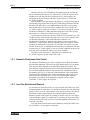
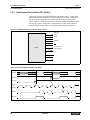
1.0 Functional Description
1.1 Functional Overview
Rockwell’s VideoStream III decoder is a high quality, single-chip solution for
processing all analog NTSC/PAL/SECAM video standards into 4:2:2 YCrCb
video. The Bt835 offers the highest price/performance of any video decoder, with
its unique 3-line adaptive comb filter, digital video input port, flexible digital
video output port, single crystal operation, and low power consumption.
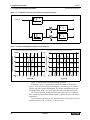
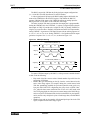
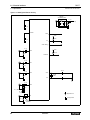
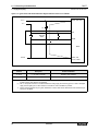
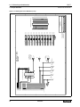
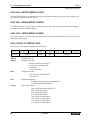
A detailed block diagram of the decoder is shown in Figure 1-1.
D835DSA
1
Bt835
1.0 Functional Description
1.1 Functional Overview
VideoStream III Decoder
CIN
REFOUT
AGCCAP
Figure 1-1. Bt835 Detailed Block Diagram
C
A/D
Y
A/D
AGC and
Sync Detect
Input Interface
MUX1
MUX2
MUX3
Oversampling
Low-Pass Filter
Y/C
Separation
D835DSA
Video Timing Control
Output Interface
LVTTL
PWRDN
OE
VD[7:0]
TDO
TDI
TMS
VD[15:8]
Digital Video
Output Formatting
JTAG
TCK
CLKx2
QCLK
Horizontal and
Vertical Filtering
and Scaling
JTAG Interface
CLKx1
CCVALID
Video Scaling
and Cropping
DIG_V
DIG_H
Clocking
Clock Interface
Digital Video
Input Formatting
Video
Adjustments
Contrast, Saturation,
and Brightness
Adjust
I2CCS
SCL
Chroma
Demod
DIG_CLK
VD[7:0]
TRST
SDA
I2C
GPIO Port
Y/C Separation and
Chroma Demodulation
I2C Interface
RST
GPIO[7:0]
2
MUX0
HRESET
VRESET
ACTIVE
VACTIVE
FIELD
CBFLAG
VALID
Bt835
1.0 Functional Description
1.1 Functional Overview
VideoStream III Decoder
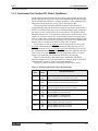
1.1.1 Bt835 Video Capture Processor for TV/VCR Analog Input
The Bt835 Video Capture Processor is a fully integrated single-chip decoding and
scaling solution for analog NTSC/PAL/SECAM input signals from TV tuners,
VCRs, cameras, and other sources of composite or Y/C video. It is the third
generation front-end input solution for low-cost PC video/graphics systems. The
Bt835 delivers complete integration and high-performance video
synchronization, Y/C separation, and filtered scaling. It has all the mixed signal
and DSP circuitry required to convert an analog composite waveform into a
scaled digital video stream, supporting a variety of video formats, resolutions,
and frame rates.
The Bt835 builds on the previous Bt829B VideoStream II decoder by adding
the following features, as detailed in Table 1-1.
Table 1-1. VideoStream III Features Options
Feature Options
Bt829B
Bt835
Composite Video Decoding
X
X
S-Video Decoding
X
X
SECAM Video
X
X
Hardware Closed-Caption Decoding
X
X
Filtered Vertical Scaling
X
X
3-line Adaptive Comb Filter
X
Single Crystal Operation for all Video Formats
X
Digital Video Input Port
X
PAL 60, NTSC 4.43 Decoding
X
8-bit GPIO
X
VIP Interface
X
1.1.2 Bt835 Architecture and Partitioning
The Bt835 provides the most cost-effective, high-quality video input solution for
low-cost multimedia subsystems that integrate both graphics display and video
capabilities. The feature set of the Bt835 supports a video/graphics system
partitioning, which optimizes the total cost of a system configured with and
without video capture capabilities. This enables system vendors to easily offer
products with graphics display and video support using a single base-system
design.
As graphics chip vendors move from PCI video/graphics processors to 3D
AGP graphics processors, the ability to efficiently use silicon and package pins to
support 2D/3D graphics acceleration, video playback acceleration, and video
capture becomes critical. This problem becomes more acute as the race toward
higher performance graphics requires more and more package pins to be
consumed for wide 128-bit memory interfaces and glueless local bus interfaces.
D835DSA
3
Bt835
1.0 Functional Description
1.1 Functional Overview
VideoStream III Decoder
The Bt835 minimizes the cost of video capture function integration in two
ways. First, recognizing that YCrCb to RGB color space conversion is a standard
feature of multimedia controllers for acceleration of digital video playback, the
Bt835 avoids redundant functionality and allows the downstream controller to
perform this task. Second, the Bt835 can minimize the number of interface pins
required by a downstream multimedia controller to keep package costs to a
minimum. This is accomplished by using industry standards interfaces such as the
VESA Video Interface Port (VIP) or the Rockwell ByteSteam™ interface.
Controller systems designed to take advantage of these features allow video
capture capability to be added to the base system in a modular fashion using only
a single Integrated Circuit (IC).
1.1.3 Comb Filter
The Bt829 video decoder and many other video decoders employ a luminance
notch filter, a chrominance bandpass filter, and a chrominance comb filter.
This means that the luminance signal is derived by filtering out the color
information (chrominance) from a composite video signal with a notch filter.
This works because the NTSC color information is in a frequency band centered
at about 3.58 MHz which extends about +/- 1.3 MHz (i.e., from 2.3 to 4.9 MHz).
The Y filter is thus designed to reject frequencies in that range. Although this
effectively filters most of the chrominance signal out of the luminance signal,
it also removes the higher frequency luminance signal components. This loss of
bandwidth reduces the horizontal resolution of the luminance signal, and fine
details in the picture are lost. The chrominance signal is derived by bandpass
filtering the composite video signal to extract the frequency band centered at
3.58 MHz which contains the color information. The Bt829 employs a
chrominance comb filter to remove any residual luminance (Y) signal that
overlaps the chrominance (C) signal in this frequency range.
Other video decoders employ a line comb filter. These line comb filters
operate by delaying the previous composite video horizontal scan line and
comparing it to the current horizontal scan line. Adding the two lines together
cancels the C signal and provides the Y signal. Subtracting the current line from
the delayed line provides the C signal. This process creates two filters which have
a frequency response that look like teeth in a comb. This type of filter is usually
known as a 1-H line comb filter, since it uses a 1-horizontal scan line delay to
process the signals. More complex filters can be built using 2-horizontal scan line
delays and are called 2-H line comb filters. While these filters will show
improvement with a multiburst test pattern compared to a notch filter, and
demonstrate a horizontal flat frequency response, the multiburst pattern does not
show that 50% of the vertical resolution is lost due to the averaging of two lines.
These filters still suffer the “hanging dot” problem noticeable on test patterns
such as the SMPTE color bar test pattern.
4
D835DSA
Bt835
1.0 Functional Description
1.1 Functional Overview
VideoStream III Decoder
In order to overcome this hanging dot problem and the loss of vertical
resolution, Rockwell has designed a sophisticated 3-line, adaptive comb filter to
separate the Y/C components in a composite video signal. This circuit is used in
the new Bt835 video decoder. As stated above, simple line comb filters can not
eliminate “hanging dots” on a vertical color transition. The problem is caused by
comb filtering two successive scan lines with different color values at the same
horizontal positions along the lines. The line comb filter cannot separate the Y/C
signals correctly in this situation. The color signal crosses over into the luminance
signal, creating the cross-luminance artifact. In a 3-line adaptive Y/C separation
filter, adaptive logic is used to continuously evaluate the video image and then
select the most efficient processing algorithm available in the filter. This is
sometimes called a 2-D filter, because both the horizontal scan lines and vertical
transitions are processed. This type of filter eliminates the hanging dot problem
by detecting the vertical transitions in the image. The logic examines three
successive horizontal scan lines simultaneously. If a vertical transition occurs
between the first and third lines, the notch filtered luminance and bandpass
filtered chrominance will be used directly, without comb filtering. Hence, two
lines with different colors will not be input to the comb filter at a transition
boundary. Therefore the Y/C signals will be fully separated and the hanging dots
eliminated. The Bt835 can accomplish this adaptive task on a pixel by pixel basis
by using powerful DSP techniques. This also ensures that the Y/C separated
image does not suffer from any loss of vertical resolution.
1.1.4 UltraLock
The Bt835 employs a proprietary technique known as UltraLock to lock to the
incoming analog video signal. It will always generate the required number of
pixels per line from an analog source in which the line length can vary by as much
as a few microseconds. UltraLock’s digital locking circuitry enables the
VideoStream™ decoders to quickly and accurately lock on to video signals,
regardless of their source. Because the technique is completely digital, UltraLock
can recognize unstable signals caused by VCR head switches or any other
deviation, and adapt the locking mechanism to accommodate the source.
UltraLock uses nonlinear techniques which are difficult, if not impossible, to
implement for genlock systems. Unlike linear techniques, it automatically adapts
the locking mechanism.
1.1.5 Scaling and Cropping
The Bt835 can independently reduce the video image size in both horizontal and
vertical directions. Using arbitrarily selected scaling ratios, the X and Y
dimensions can be scaled down to one-sixteenth of the full resolution. Horizontal
scaling is implemented with a six-tap interpolation filter, while a maximum of
five-tap interpolation is used for vertical scaling with a line store.
The video image can be arbitrarily cropped by programming the ACTIVE flag
to reduce the number of active scan lines and active horizontal pixels per line.
The Bt835 also supports a temporal decimation feature that reduces video
bandwidth by allowing frames or fields to be dropped from a video sequence at
regular, but arbitrarily selected, intervals.
D835DSA
5
Bt835
1.0 Functional Description
1.1 Functional Overview
VideoStream III Decoder
1.1.6 Input Interfaces
Analog Video Input
Analog video signals are input to the Bt835 via a four-input multiplexer that can
select between four composite source inputs, or between three composite input
sources and a single S-Video input source. When an S-Video source is input to
the Bt835, the luma component is fed through the input analog multiplexer, and
the chroma component is fed directly into the C input pin. An AGC circuit
enables the Bt835 to compensate for reduced amplitude in the analog signal input.
The clock signal interface consists of two pins for crystal connection and two
clock output pins. These crystal pins connect to any standard 14.318 MHz,
low-jitter (50 ppm or better) crystal for NTSC /PAL/SECAM operation. The
on-board PLL circuit generates output clocks for interface to the graphics
controller or frame buffer. CLKx2 is output at full frequency (8*Fsc), whereas
CLKx1 operates at half the synthesized crystal frequency (4*Fsc). Either crystals
or CMOS oscillators may be used for the clock source.
Digital Video Input
The Bt835 will accept digital video data as 8-bit, 26-30 MHz 4:2:2 YCrCb
samples on the VD[7:0] pins. The digital video clock (DIG_CLK) can be
configured either as an input or output for slave or master mode timing. Timing
and synchronization control is provided by the DIG_H and DIG_V pins. These
pins are not required if the video source has CCIR656 timing with embedded
SAV, EAV timing codes. When accepting digital video, the Bt835 can control
contrast, saturation, and brightness. There is no provision for hue adjustment.
1.1.7 Output Interface
The Bt835 supports a Synchronous Pixel Interface (SPI) mode.
The SPI supports a YCrCb 4:2:2 data stream over an 8- or 16-bit wide path.
When the pixel output port is configured to operate 8 bits wide, 8 bits of
chrominance data are output on the first clock cycle, followed by 8 bits of
luminance data on the next clock cycle for each pixel. Two clocks are required to
output one pixel in this mode, and so a 2x clock is used to output the data.
The Bt835 outputs all horizontal and vertical blanking pixels, in addition to
the active pixels synchronous with CLKX1 (16-bit mode) or CLKX2 (8-bit
mode). It is possible to insert control codes into the pixel stream using
chrominance and luminance values that are outside the allowable chroma and
luma ranges. These control codes can be used to flag video events such as
ACTIVE, HRESET, and VRESET. Decoding these video events downstream
enables the video controller to eliminate pins required for the corresponding
video control signals.
The Bt835 supports the VESA VIP interface and the Rockwell ByteStream
interface for embedding control codes into the digital video pixel stream.
6
D835DSA
Bt835
1.0 Functional Description
1.1 Functional Overview
VideoStream III Decoder
1.1.8 VBI Data Pass-through
The Bt835 provides VBI data passthrough capability. The VBI region ancillary
data is captured by the video decoder and is made available to the system for
subsequent software processing. The Bt835 may operate in a VBI line output
mode, in which the VBI data is only made available during select lines. This mode
of operation is intended to enable capture of VBI lines containing ancillary data,
as well as processing normal YCrCb video image data. In addition, the Bt835
supports a VBI frame output mode, in which every line in the video signal is
treated as if it were a vertical interval line, and no image data is output. This mode
of operation is designed for use in still-frame capture/processing applications.
In VIP mode, the Bt835 passes VBI data raw samples. During selected VBI
lines, the VIP task bit T is set. The protection bits P[3:0] are not used and are
forced to 0. Ancillary data is not supported. This mode is controlled by the
VIPEN bit.
1.1.9 Closed Caption Decoding
The Bt835 provides a Closed Captioning (CC) and Extended Data Services
(EDS) decoder. Data presented to the video decoder on the CC and EDS lines is
decoded and made available to the system through the CC_DATA and
CCSTATUS registers.
1.1.10 I2C Interface
The Bt835 registers are accessed via a two-wire I2C interface. The Bt835 operates
as a slave device. Serial clock and data lines SCL and SDA transfer data from the
bus master at a maximum rate of 100 kbps. Chip select and reset signals are also
available to select one of two possible Bt835 devices in the same system, and to
set the registers to their default values.
1.1.11 3.3 V/5 V Operation
The Bt835 can interface to either 5 V or 3.3 V signal level graphics/system
controllers. When in 5 V mode, all power pins should be tied to +5 V levels.
LVTTL must also be tied to +5 V.
When in 3.3 V mode, the digital inputs/outputs are not 5 V tolerant, they can
only interface to 3.3 V signal levels. When in 3.3 V mode, all VDD, VPP, and
VDDO pins must be tied to 3.3 V, all VAA pins must be tied to +5 V (for ADC
biasing). LVTTL must be tied to ground.
D835DSA
7
Bt835
1.0 Functional Description
1.2 Pin Descriptions
VideoStream III Decoder
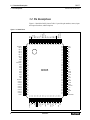
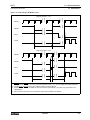
1.2 Pin Descriptions
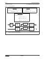
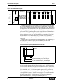
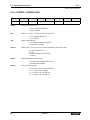
Figure 1-2 details the Bt835 pinout. Table 1-2 provides pin numbers, names, input
and output functions, and descriptions.
8
SDA
SCL
TDI
TDO
TMS
TCK
TRST
TWREN
VSS/GND
88
87
86
85
84
83
82
81
90
89
VSSO/GND
VDDO
91
LVTTL
PWRDN
VPP
94
92
XTI
95
93
PGND
XTO
12CCS
98
96
RST
99
97
VDD
100
Figure 1-2. Bt835 Pinout
VSS/GND
1
80
VDD
VD[15]
2
79
FRST
VD[14]
3
78
NC
VD[13]
4
77
NC
VD[12]
5
76
NC
VD[11]
6
75
NC
VD[10]
7
74
NC
VD[9]
8
73
NC
VD[8]
9
72
NC
VDDO
10
71
NC
VSSO/GND
11
70
NC
VD[7]
12
69
NC
VD[6]
13
68
NC
VD[5]
14
67
NC
VD[4]
15
66
VAA
VD[3]
16
65
MUX3
VD[2]
17
64
AGND
VD[1]
18
63
MUX2
VD[0]
19
62
VAA
VDD
20
61
MUX1
VSS/GND
21
60
VAA
GPIO[7]
22
59
MUX0
GPIO[6]
23
58
AGND
GPIO[5]
24
57
REFP
GPIO[4]
25
56
AGCCAP
GPIO[3]
26
55
VAA
GPIO[2]
27
54
CIN
GPIO[1]
28
53
AGND
GPIO[0]
29
52
NC
VDDO
30
51
VSSO/GND
44
45
46
47
48
49
50
CBFLAG
DIG_H
DIG_V
NC
DIG_CLK
VDDO
43
D835DSA
CCVALID
42
38
VACTIVE
QCLK
37
ACTIVE
FIELD
36
VRESET
41
35
40
34
CLKx1
HRESET
VDD
VSS/GND
33
OE
39
32
CLKx2
VALID
31
VSSO/GND
Bt835
Bt835
1.0 Functional Description
1.2 Pin Descriptions
VideoStream III Decoder
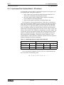
Table 1-2. Bt835 Pin Descriptions (1 of 2)
Pin #
I/O
Pin Name
Description
9–2
O
VD[15:8]
In 16-bit output mode, these pins represent the luma portion of the decoded
video signal. In 8-bit output mode, these pins are the 4:2:2 multiplexed data
stream. In test mode, these pins may be configured to be the test bus output.
19–12
I/O
VD[7:0]
In 16-bit mode, these pins represent the multiplexed Cr/Cb portion of the
decoded video signal. In 8-bit mode, these pins are three-stated. When in 8-bit
mode, these pins may be used to input digital video. In test mode, these pins are
used as the test bus input.
29–22
I/O
GPIO[7:0]
These pins are used to control, or sample, external devices. These pins will power
up three-stated.
32
O
CLKx2
33
I
OE
34
O
CLKx1
ADC sample clock, divided by two.
35
O
HRESET
Active low. Horizontal reset output.
36
O
VRESET
Active low. Vertical reset output.
37
O
ACTIVE
Composite active video region. Indicates non-blanked region of decoded video.
May be configured to represent the horizontal active region of each line.
38
O
VACTIVE
Vertical active output. Indicates the non-blanked vertical region of the decoded
video.
39
O
VALID
Valid pixel output. This signal, in conjunction with ACTIVE, indicates which pixels
will be used in the construction of the decoded video field/frame. May be
internally and logically ANDED with the ACTIVE pin.
42
O
QCLK
Gated output clock. In 16-bit mode, this pin is created by inverting and gating the
CLKX1 clock. In 8-bit mode, the CLKx2 clock is used.
43
O
FIELD
Even Field indicator.
44
O
CBFLAG
Cb pixel indicator.
45
O
CCVALID
Open drain output. Indicates that the CC FIFO has CC data to be read. If used,
must be externally pulled up.
46
I
DIG_H
Digital video horizontal reset input. Can be tied high/low if not used.
47
I
DIG_V
Digital video vertical reset input. Can be tied high/low if not used.
49
I/O
DIG_CLK
Digital video clock. May be configured as either input or output. Bidirectional. Do
not tie if not used.
79
I
FRST
Active HIGH FIFO reset. Used for testing purposes only. JTAG. Tie high for normal
use.
82
I
TWREN
83
I
TRST
Active low. JTAG reset. Tie low for normal use.
84
I
TCK
JTAG clock. Tie low for normal use.
85
I
TMS
JTAG test mode select. Tie high for normal use.
ADC sample clock output.
Active low output enable. When pulled high, this pin will three-state the pins
defined by the OES[1:0] register bits. This pin works in conjunction with the
NOUTEN register bit. When either NOE or OUTEN is high, the selected pins will be
three-stated.
FIFO test-write input. JTAG pin. Tie low for normal use.
D835DSA
9
Bt835
1.0 Functional Description
1.2 Pin Descriptions
VideoStream III Decoder
Table 1-2. Bt835 Pin Descriptions (2 of 2)
Pin #
I/O
Pin Name
86
O
TDO
JTAG test data out. Do not connect this pin for normal use.
87
I
TDI
JTAG test data in. Tie high for normal use.
88
I
SCL
I2C clock.
89
I/O
SDA
I2C data. Open drain I/O. Must be externally pulled up, typically with a 10 kΩ
resistor.
92
I
PWRDN
93
I
LVTTL
95
I
XTI
Crystal in.
96
I
XTO
Crystal out.
98
I
I2CCS
99
I
RST
When low, resets the Bt835. Internal pullup.
20, 40, 80,
100
P
VDD
Core power. Can be connected to 3.3 V or 5 V.
1, 21, 41,
81
G
VSS
Core ground. Must be connected to ground.
10, 30, 50,
90
P
VDDO
Pad ring power.
11, 31, 51,
91
G
VSSO/GND
Pad ring ground.
94
P
VPP
PLL power.
97
G
PGND
PLL ground.
55, 60, 66
P
VAA
53, 58, 64
G
AGND
54
I
CIN
57
I
REFP
56
I
AGCCAP
The AGC time-constant control. Must be connected to a 0.1 µF capacitor to
ground.
59, 61, 63,
65
I
MUX[3:0]
Analog composite video inputs to the on-chip input multiplexer. They are used to
select between four composite sources or three composite and one S-Video
source. Unused pins should be connected to GND.
10
Description
Powers down the decoder when high.
When connected to ground, configures the Bt835 to operate at 3.3 V. When
connected to VDD, configures the Bt835 to operate at 5 V.
Used to select alternate I2C address. High = 0x8A; low = 0x88.
Analog power. Must always be connected to 5 V.
Analog ground. Must always be connected to ground.
The analog chroma input to the C-ADC.
The top of the ADC reference must be connected to a 0.1 µF input capacitor to
ground.
D835DSA
Bt835
1.0 Functional Description
1.3 UltraLock
VideoStream III Decoder
1.3 UltraLock
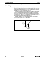
1.3.1 The Challenge
The line length (the interval between the midpoints of the falling edges of
succeeding horizontal sync pulses) of analog video sources is not constant. For a
stable source such as a studio grade video source or test signal generators, this
variation is very small: ±2 ns. For an unstable source such as a VCR, laser disk
player, or TV tuner, line length variation can be a few microseconds.
Despite these variations, digital display systems require a fixed number of
pixels per line. The Bt835 employs the UltraLock technique to lock to the
horizontal sync and the subcarrier of the incoming analog video signal, and to
generate the required number of pixels per line.
1.3.2 Operation Principles of UltraLock
UltraLock is based on sampling, using a fixed-frequency stable clock. Because
the video line length varies, the number of samples generated using a
fixed-frequency sample clock also varies from line to line. If the number of
generated samples per line is always greater than the number of samples per line
required by the particular video format, the number of acquired samples can be
reduced to fit the required number of pixels per line.
The Bt835 PLL generates a 8*Fsc (28.64 MHz for NTSC and 35.47 MHz for
PAL) clock from a crystal or oscillator input signal source. The 8*Fsc clock
signal, or CLKx2, is divided down to CLKx1 internally (14.32 MHz for NTSC
and 17.73 MHz for PAL). Both CLKx2 and CLKx1 are made available to the
system. UltraLock operates at CLKx1, although the input waveform is sampled at
CLKx2, then low-pass filtered, and decimated to a CLKx1 sample rate.
A 4*Fsc (CLKx1) sample rate produces 910 pixels for NTSC and 1,135 pixels
for PAL/SECAM within a nominal line time interval (63.5 µs for NTSC and 64
µs for PAL/SECAM). Square pixel NTSC and PAL/SECAM formats should
produce only 780 and 944 pixels per video line, respectively. This is because the
square pixel clock rates are slower than a 4*Fsc clock rate, i.e., 12.27 MHz for
NTSC, and 14.75 MHz for PAL.
UltraLock accommodates line length variations from nominal time line
intervals in the incoming video by always acquiring more samples (at an effective
4*Fsc rate) than the particular video format requires. UltraLock interpolates to
the required number of pixels so that it maintains the stability of the original
image, despite variation in the line length of the incoming analog waveform.
The example illustrated in Figure 1-3 shows three successive lines of video
being decoded for square pixel NTSC output. The first line is shorter than the
nominal NTSC line time interval of 63.5 µs. On this first line, a line time of 63.2
µs sampled at 4*Fsc (14.32 MHz) generates only 905 pixels. The second line
matches the nominal line time of 63.5 µs and provides the expected 910 pixels.
Finally, the third line is too long at 63.8 µs, within which 913 pixels are generated.
In all three cases, UltraLock outputs only 780 pixels.
D835DSA
11
Bt835
1.0 Functional Description
1.3 UltraLock
VideoStream III Decoder
Figure 1-3. UltraLock Behavior for NTSC Square Pixel Output
Analog
Waveform
Line
Length
Pixels
Per Line
Pixels
Sent to
the Pixel
Bus by
UltraLock
63.2 µs
63.5 µs
63.8 µs
905 pixels
910 pixels
913 pixels
780 pixels
780 pixels
780 pixels
UltraLock can be used to extract any programmable number of pixels from the
original video stream, as long as the sum of the nominal pixel line length, 910 for
NTSC and 1,135 for PAL/SECAM, and the worst case line length variation in the
active region is greater than or equal to the required number of output pixels per
line, i.e.,
P Nom + P Var ≥ P Desired
where:
PNom
= Nominal number of pixels per line at 4*Fsc sample rate
(910 for NTSC, 1,135 for PAL/SECAM)
PVar
= Variation of pixel count from nominal at 4*Fsc (can be a
positive or negative number)
PDesired = Desired number of output pixels per line
NOTE(S): For stable inputs, UltraLock guarantees the time between the falling edges of HRESET to
within only one pixel. UltraLock guarantees the number of active pixels in a line, as long
as the above relationship holds.
12
D835DSA
Bt835
1.0 Functional Description
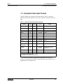
1.4 Composite Video Input Formats
VideoStream III Decoder
1.4 Composite Video Input Formats
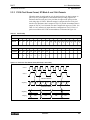
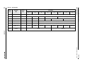
The Bt835 supports all composite video input formats. Table 1-3 shows the
different video formats and shows some of the countries in which each format is
used.
Table 1-3. Video Input Formats Supported by the Bt835
Format
Lines
Fields
FSC
Country
NTSC-M
525
60
3.58 MHz
U.S., many others
NTSC-Japan(1)
525
60
3.58 MHz
Japan
PAL-B
625
50
4.43 MHz
Many
PAL-D
625
50
4.43 MHz
China
PAL-G
625
50
4.43 MHz
Many
PAL-H
625
50
4.43 MHz
Belgium
PAL-I
625
50
4.43 MHz
Great Britain, others
PAL-M
525
60
3.58 MHz
Brazil
PAL-N
625
50
4.43 MHz
Paraguay, Uruguay
PAL-N
combination
625
50
3.58 MHz
Argentina
SECAM
625
50
4.406 MHz
4.250 MHz
Eastern Europe, France,
Middle East
PAL–60(2)
525
60
4.43 MHz
China
NTSC(4.43)
525
60
4.43 MHz
Transcoding Application
(1) NTSC-Japan has 0 IRE setup.
(2) Typically used in Chinese Video CD players.
The video decoder must be appropriately programmed for each of the
composite video input formats. Table 1-4 lists the register values that need to be
programmed for each input format.
D835DSA
13
Bit
NTSC-M
NTSC-Japan
PAL-B,
D, G, H, I
PAL-M
PAL-N
PAL-N
Combination
PAL-60
SECAM
NTSC
4.43
D835DSA
INPUT
(0x01)
FMT[3:0]
0001
0010
0100
0101
0110
0111
1000
1001
0011
Cropping:
HDELAY,
VDELAY,
VACTIVE,
CROP
7:0 in all 5
registers
Set to desired
cropping
values in
registers
Set to NTSC-M
square pixel
values
Set to desired
cropping
values in
registers
Set to NTSC-M
square pixel
values
Set to PAL-B,
D, G, H, I
square pixel
values
Set to PAL-B,
D, G, H, square
pixels values
Set to PAL-B,
D, G, H, I
square pixel
values
Set to PAL-B,
D, G, H, I
square pixel
values
Set to
NTSC-M
square
pixel
values
HSCALE
(0x0A, 0x09)
15:0
0x02AA
0x02AA
0x033C
0x02AA
0x033C
0x00F8
0x02AA
0x033C
0x02AA
ADELAY
(0x1A)
7:0
0x68
0x68
0x7F
0x68
0x7F
0x7F
0x68
0x7F
0x68
BDELAY
(0x1B)
7:0
0x5D
0x5D
0x72
0x5D
0x72
0x72
0x5D
0xA0
0x5D
1.0 Functional Description
Register
1.4 Composite Video Input Formats
14
Table 1-4. Register Values for Video Input Formats
Bt835
VideoStream III Decoder
Bt835
1.0 Functional Description
1.5 Y/C Separation and Chroma Demodulation
VideoStream III Decoder
1.5 Y/C Separation and Chroma Demodulation
Y/C separation and chroma decoding are handled as shown in Figure 1-4 and
Figure 1-5. A 3-line adaptive comb filter is used to separate luminance and
chrominance for NTSC video. A notch/band-pass filter is used for PAL/SECAM
video. Figure 1-6 displays the filter responses. The optional chroma comb filter,
when using notch filter, is implemented in the vertical scaling block. See the
section on Video Scaling, Cropping, and Temporal Decimation in this chapter.
Figure 1-4. Y/C Separation and Chroma Demodulation for Composite NTSC Video
Composite
Y
Notch Filter
Luma Switch
Adaptive Logic
and Vertical
Transition Detector
Luma Comb
Video Delay
U
Low-Pass Filter
Band-Pass Filter
sin
V
Low-Pass Filter
cos
D835DSA
15
Bt835
1.0 Functional Description
1.5 Y/C Separation and Chroma Demodulation
VideoStream III Decoder
Figure 1-5. Y/C Separation and Chroma Demodulation for Composite PAL Video
Y
Composite
Notch Filter
U
Low-Pass Filter
sin
V
Low-Pass Filter
Band-Pass Filter
cos
Figure 1-6. NTSC and PAL/SECAM Y/C Separation Filter Responses
Luma Notch Filter Frequency Responses for NTSC and PAL/SECAM
Chroma Band Pass Filter Frequency Responses for NTSC and PAL/SECAM
NTSC
NTSC
PAL/SECAM
PAL/SECAM
Figure 1-7 describes the filtering and scaling operations.
In addition to the Y/C separation and chroma demodulation illustrated in
Figure 1-5, the Bt835 also supports chrominance comb filtering as an optional
filtering stage after chroma demodulation. The chroma demodulation generates
baseband I and Q (NTSC) or U and V (PAL/SECAM) color difference signals.
For S-Video operation, the digitized luma data bypasses the Y/C separation
block completely, and the digitized chrominance is passed directly to the chroma
demodulator.
For monochrome operation, the Y/C separation block is also bypassed, and the
saturation registers (SAT_U and SAT_V) are set to zero.
16
D835DSA
Bt835
1.0 Functional Description
1.5 Y/C Separation and Chroma Demodulation
VideoStream III Decoder
Figure 1-7. Filtering and Scaling
Horizontal Scaler
Luminance
= A + BZ
–1
+ CZ
Chrominance
–2
+ DZ
Vertical Scaler
–3
= G + HZ
+ EZ
–4
+ FZ
–5
Luminance
–1
= C + DZ
Chrominance
–1
1 1 –1
= --- + --- Z
(Chroma Comb)
2 2
Vertical Filter Options
–1
1
Luminance = --- ( 1 + z )
2
–1
–2
1
= --- ( 1 + 2 Z + 1 Z )
4
–1
–2
–3
1
= --- ( 1 + 3 Z + 3 Z + 1 Z )
8
–1
–2
–3
–4
1
= ------ ( 1 + 4 Z + 6 Z + 4 Z + Z )
16
Y
C
Note:
Optional
3 MHz
Horizontal
Low-Pass
Filter
6-Tap, 32-Phase
Interpolation
and
Horizontal
Scaling
On-chip Memory
2-Tap, 32-Phase
Interpolation
and
Horizontal
Scaling
On-chip Memory
Luma Comb
Vertical Scaling
Vertical Filtering
Y
Chroma Comb
and
Vertical Scaling
C
Z–1 refers to a pixel delay in the horizontal direction, and a line delay in the vertical direction. The coefficients are determined by UltraLock and the scaling algorithm.
D835DSA
17
Bt835
1.0 Functional Description
1.6 Video Scaling, Cropping, and Temporal Decimation
VideoStream III Decoder
1.6 Video Scaling, Cropping, and Temporal
Decimation
The Bt835 provides three mechanisms to reduce the amount of video pixel data in
its output stream: down-scaling, cropping, and temporal decimation. All three can
be controlled independently.
1.6.1 Horizontal and Vertical Scaling
The Bt835 provides independent and arbitrary horizontal and vertical downscaling. The maximum scaling ratio is 16:1 in both X and Y dimensions. The
maximum vertical scaling ratio is reduced from 16:1 when using frames to 8:1.
The following sections describe the different methods used for scaling luminance
and chrominance.
1.6.2 Luminance Scaling
The first stage in horizontal luminance scaling is an optional pre-filter which
provides the capability to reduce anti-aliasing artifacts. It is generally desirable to
limit the bandwidth of the luminance spectrum prior to performing horizontal
scaling. This is because the scaling of high-frequency components may create
image artifacts in the resized image. The optional low-pass filters shown in
Figure 1-8 reduce the horizontal high-frequency spectrum in the luminance
signal. Figures 1-9 and 1-10 show the combined results of the optional low-pass
filters, and the luma notch and 2x oversampling filter.
Figure 1-8. Optional Horizontal Luma Low-Pass Filter Responses
NTSC
PAL/SECAM
QCIF
QCIF
CIF
ICON
ICON
18
D835DSA
CIF
Bt835
1.0 Functional Description
1.6 Video Scaling, Cropping, and Temporal Decimation
VideoStream III Decoder
Figure 1-9. Combined Luma Notch, 2x Oversampling and Optional Low-Pass Filter Response (NTSC)
Pass Band
Full Spectrum
QCIF
CIF
ICON
CIF
ICON
QCIF
Figure 1-10. Combined Luma Notch, 2x Oversampling and Optional Low-Pass Filter Response (PAL/SECAM)
CIF
Full Spectrum
Pass Band
QCIF
CIF
ICON
QCIF
ICON
The Bt835 implements horizontal scaling through poly-phase interpolation.
The Bt835 uses 32 different phases to accurately interpolate the value of a pixel.
This provides an effective pixel jitter of less than 6 ns.
In simple pixel- and line-dropping algorithms, non-integer scaling ratios
introduce a step function in the video signal that effectively introduces highfrequency spectral components. Poly-phase interpolation accurately interpolates
to the correct pixel and line position, providing more accurate information. This
results in more aesthetically pleasing video, as well as higher compression ratios
in bandwidth-limited applications.
For vertical scaling, the Bt835 uses a line store to implement four different
filtering options. The filter characteristics are shown in Figure 1-11. The Bt835
provides up to 5-tap filtering to ensure removal of aliasing artifacts. Figure 1-12
shows the combined responses of the luma notch and 2x oversampling filters.
D835DSA
19
Bt835
1.0 Functional Description
1.6 Video Scaling, Cropping, and Temporal Decimation
VideoStream III Decoder
Figure 1-11. Frequency Responses for the Four Optional Vertical Luma Low-Pass Filters
2-tap
3-tap
4-tap
5-tap
Figure 1-12. Combined Luma Notch and 2x Oversampling Filter Response
PAL/SECAM
NTSC
20
D835DSA
Bt835
1.0 Functional Description
1.6 Video Scaling, Cropping, and Temporal Decimation
VideoStream III Decoder
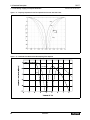
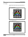
1.6.3 Peaking
The Bt835 enables four different peaking levels by programming the PSEL[1:0]
bits in the CONTROL_0 register. The filter responses are shown in Figures 1-13
and 1-14.
Figure 1-13. NTSC Peaking Filters
Peaking Filters
8
7
6
Amplitude (dB)
5
4
3
2
1
0
-1
-2
-3
0
1
2
3
4
5
6
7
Frequency (Fs = 14.3182 MHz)
Figure 1-14. PAL/SECAM Peaking Filters
Peaking Filters
8
7
6
Amplitude (dB)
5
4
3
2
1
0
-1
-2
-3
0
1
2
D835DSA
3
4
5
6
7
8
Frequency (Fs = 17.7345 MHz)
21
Bt835
1.0 Functional Description
1.6 Video Scaling, Cropping, and Temporal Decimation
VideoStream III Decoder
The number of taps in the vertical filter is set by the VSCALE_CTL register.
The user may select 2, 3, 4, or 5 taps. The number of taps must be chosen in
conjunction with the horizontal scale factor. As the scaling ratio is increased, the
number of taps available for vertical scaling is increased. In addition to low-pass
filtering, vertical interpolation is also employed to minimize artifacts when
scaling to non-integer scaling ratios.
1.6.4 Chrominance Scaling
A 2-tap, 32-phase interpolation filter is used for horizontal scaling of
chrominance. Vertical scaling of chrominance is implemented through
chrominance comb filtering using a line store, followed by simple decimation or
line dropping.
1.6.5 Scaling Registers
Horizontal Scaling Ratio Register (HSCALE) HSCALE is programmed with the
horizontal scaling ratio. When outputting unscaled video (in NTSC), the Bt835
will produce 910 pixels per line. This corresponds to the pixel rate at fCLKx1
(4*Fsc). This register is the control for scaling the video to the desired size. For
example, square pixel NTSC requires 780 samples per line, while CCIR601
requires 858 samples per line. HSCALE_HI and HSCALE_LO are two 8-bit
registers that, when concatenated, form the 16-bit HSCALE register.
The method below uses pixel ratios to determine the scaling ratio. The
following formula is used to determine the scaling ratio to be entered into the 16bit register:
NTSC:
HSCALE = [ ( 910/Pdesired ) – 1] * 4096
PAL/SECAM: HSCALE = [ ( 1135/Pdesired ) – 1] * 4096
where:
Pdesired
= Desired number of pixels per line of video, including active, sync, and blanking.
For example, to scale PAL/SECAM input to square pixel QCIF, the total number
of horizontal pixels is 236:
HSCALE = [ ( 1135/236 ) – 1 ] * 4096
= 15602
= 0x3CF2
An alternative method for determining the HSCALE value uses the ratio of the
scaled active region to the unscaled active region as shown below:
NTSC:
PAL/SECAM:
where:
22
HSCALE = [ (754 / HACTIVE) – 1] * 4096
HSCALE = [ (922 / HACTIVE) – 1] * 4096
HACTIVE = Desired number of pixels per line of video, not including sync or blanking.
D835DSA
Bt835
1.0 Functional Description
1.6 Video Scaling, Cropping, and Temporal Decimation
VideoStream III Decoder
In this equation, the HACTIVE value cannot be cropped; it represents the total
active region of the video line. This equation produces roughly the same result as
using the full line length ratio shown in the first example. However, due to
truncation, the HSCALE values determined using the active pixel ratio will be
slightly different than those obtained using the total line length pixel ratio. The
values in Table 1-5 were calculated using the full line length ratio.
Table 1-5. Scaling Ratios for Popular Formats Using Frequency Values
Scaling Ratio
Format
Total
Resolution
(including
sync and
blanking
interval)
Output
Resolution
(Active Pixels)
HSCALE
Register
Values
VSCALE Register
Values
Use Both
Fields
Single
Field
Full Resolution
1:1
NTSC SQ Pixel
NTSC CCIR601
PAL CCIR601
PAL SQ Pixel
780 x 525
858 x 525
864 x 625
944 x 625
640 x 480
720 x 480
720 x 576
768 x 576
02aa
00F8
0504
033C
0000
0000
0000
0000
1E00
1E00
1E00
1E00
CIF
2:1
NTSC SQ Pixel
NTSC CCIR601
PAL CCIR601
PAL SQ Pixel
390 x 262
429 x 262
432 x 312
472 x 312
320 x 240
360 x 240
360 x 288
384 x 288
1555
11F0
1A09
1677
1E00
1E00
1E00
1E00
1A00
1A00
1A00
1A00
QCIF
4:1
NTSC SQ Pixel
NTSC CCIR601
PAL CCIR601
PAL SQ Pixel
195 x 131
214 x 131
216 x 156
236 x 156
160 x 120
180 x 120
180 x 144
192 x 144
3AAA
3409
4412
3CF2
1A00
1A00
1A00
1A00
1200
1200
1200
1200
ICON
8:1
NTSC SQ Pixel
NTSC CCIR601
PAL CCIR601
PAL SQ Pixel
97 x 65
107 x 65
108 x 78
118 x 78
80 x 60
90 x 60
90 x 72
96 x 72
861A
7813
9825
89E5
1200
1200
1200
1200
0200
0200
0200
0200
1. PAL-M–HSCALE and VSCALE register values should be the same for NTSC.
2. SECAM–HSCALE and VSCALE register values should be the same as for PAL.
Vertical Scaling Ratio Register (VSCALE) VSCALE is programmed with the
vertical scaling ratio. It defines the number of vertical lines output by the Bt835.
The following formula should be used to determine the value to be entered into
this 13-bit register. The loaded value is a two’s-complement, negative value.
VSCALE = ( 0x10000 – { [ ( scaling_ratio ) – 1] * 512 } ) & 0x1FFF
For example, to scale PAL/SECAM input to square pixel QCIF, the total number
of vertical lines for PAL square pixel is 156 (see Table 1-5).
VSCALE = ( 0x10000 – { [ ( 4/1 ) –1 ] * 512 } ) & 0x1FFF
= 0x1A00
NOTE(S): Only the 13 least significant bits of the VSCALE value are used. The user must take care
not to alter the values of the three most significant bits when writing a vertical scaling
value.
D835DSA
23
Bt835
1.0 Functional Description
1.6 Video Scaling, Cropping, and Temporal Decimation
VideoStream III Decoder
When vertical scaling (below CIF resolution), it may be useful to use a single
field, as opposed to using both fields. Using a single field ensures that no interfield motion artifacts occur on the scaled output. When performing single field
scaling, the vertical scaling ratio is twice as large as when scaling with both
fields. For example, CIF scaling from one field does not require any vertical
scaling, but when scaling from both fields, the scaling ratio is 50%. The noninterlaced bit should be reset when scaling from a single field (NVINT = 0 in the
VSCALE_CTL register). Table 1-5 lists scaling ratios for various video formats
and the register values required.
1.6.6 Image Cropping
Cropping enables the user to output any subsection of the video image. The
ACTIVE flag can be programmed to start and stop at any position on the video
frame as shown in Figure 1-15. The start of the active area in the vertical direction
is referenced to VRESET (beginning of a new field). In the horizontal direction, it
is referenced to HRESET (beginning of a new line). The dimensions of the active
video region are defined by HDELAY, HACTIVE, VDELAY, and VACTIVE. The
vertical and horizontal delay values determine the position of the cropped image
within a frame, while the horizontal and vertical active values set the pixel
dimensions of the cropped image, as illustrated in Figure 1-15.
24
D835DSA
Bt835
1.0 Functional Description
1.6 Video Scaling, Cropping, and Temporal Decimation
VideoStream III Decoder
VDELAY
Video Frame
VACTIVE
Cropped image
VDELAY
HDELAY
HACTIVE
Video Frame
VACTIVE
Rising edge of VRESET
Figure 1-15. Effect of the Cropping and Active Registers
Cropped Image
Scaled to
1/2 Size
HDELAY
HACTIVE
Falling Edge of HRESET
D835DSA
25
Bt835
1.0 Functional Description
1.6 Video Scaling, Cropping, and Temporal Decimation
VideoStream III Decoder
1.6.7 Cropping Registers
Horizontal Delay Register (HDELAY) HDELAY is programmed with the delay
between the falling edge of HRESET and the rising edge of ACTIVE. The count
is programmed with respect to the scaled frequency clock. HDELAY should
always be an even number.
Horizontal Active Register (HACTIVE) HACTIVE is programmed with the actual
number of active pixels per line of video. This is equivalent to the number of
scaled pixels that the Bt835 should output on a line. For example, if this register
contained 90, and HSCALE was programmed to down-scale by 4:1, then 90
active pixels would be output. The 90 pixels would be a 4:1 scaled image of the
360 pixels (at CLKx1), starting at count HDELAY. HACTIVE is restricted in the
following manner:
HACTIVE + HDELAY ≤ Total Number of Scaled Pixels.
For example, in the NTSC square pixel format, there is a total of 780 pixels,
including blanking, sync and active regions. Therefore:
HACTIVE + HDELAY ≤780.
When scaled by 2:1 for CIF, the total number of active pixels is 390.
Therefore:
HACTIVE +HDELAY ≤390.
The HDELAY register is programmed with the number of scaled pixels
between HRESET and the first active pixel. Because the front porch is defined as
the distance between the last active pixel and the next horizontal sync, the video
line can be considered in three components: HDELAY, HACTIVE, and the front
porch. Figure 1-16 illustrates the video signal regions.
Figure 1-16. Regions of the Video Signal
HDELAY
Front
Porch
HACTIVE
Table 1-6 shows the number of clocks at the 4x sample rate (the CLKx1 rate)
when cropping is not implemented.
Table 1-6. Uncropped Clock Totals
26
CLKx1
Front Porch
CLKx1
HDELAY
CLKx1
HACTIVE
CLKx1
Total
NTSC
21
135
754
910
PAL/SECAM
27
186
922
1135
D835DSA
Bt835
1.0 Functional Description
1.6 Video Scaling, Cropping, and Temporal Decimation
VideoStream III Decoder
The value for HDELAY is calculated using the following formula:
HDELAY = [(CLKx1_HDELAY / CLKx1_HACTIVE) * HACTIVE] & 0x3FE
CLKx1_HDELAY and CLKx1_HACTIVE are constant values, so the
equation becomes:
NTSC: HDELAY = [(135 / 754) * HACTIVE] & 0x3FE
PAL/SECAM: HDELAY = [(186 / 922) * HACTIVE] & 0x3FE
In this equation, the HACTIVE value cannot be cropped.
Vertical Delay Register (VDELAY) VDELAY is programmed with the delay
between the rising edge of VRESET and the start of active video lines. It
determines how many lines to skip before initiating the ACTIVE signal, and is
programmed with the number of lines to skip at the beginning of a frame.
Vertical Active Register (VACTIVE) VACTIVE is programmed with the number
of lines used in the vertical scaling process. The actual number of vertical lines
output from the Bt835 is equal to this register, multiplied by the vertical scaling
ratio. If VSCALE is set to 0x1A00 (4:1), then the actual number of lines output is
VACTIVE/4. If VSCALE is set to 0x0000 (1:1), then VACTIVE contains the
actual number of vertical lines output.
NOTE(S): It is important to note the difference between the implementation of the horizontal
registers (HSCALE, HDELAY, and HACTIVE) and the vertical registers (VSCALE, VDELAY,
and VACTIVE). Horizontally, HDELAY and HACTIVE are programmed with respect to the
scaled pixels defined by HSCALE. Vertically, VDELAY and VACTIVE are programmed
with respect to the number of lines before scaling (before VSCALE is applied).
D835DSA
27
Bt835
1.0 Functional Description
1.6 Video Scaling, Cropping, and Temporal Decimation
VideoStream III Decoder
1.6.8 Temporal Decimation
Temporal decimation provides a solution for video synchronization during
periods when full frame rate cannot be supported due to bandwidth and system
restrictions.
For example, when capturing live video for storage, system limitations such as
hard disk transfer rates or system bus bandwidth may limit the frame capture rate.
If these restrictions limit the frame rate to 15 frames per second, the Bt835’s time
scaling operation enables the system to capture every other frame, instead of
allowing the hard disk timing restrictions to dictate which frame to capture. This
maintains an even distribution of captured frames and alleviates the jerky effects
caused by systems that simply burst in data when bandwidth becomes available.
The Bt835 provides temporal decimation on either a field or frame basis. The
temporal decimation register (TDEC) is loaded with a value from 1 to 60 (NTSC)
or 1 to 50 (PAL/SECAM). This value represents the number of fields or frames
skipped by the chip during a sequence of 60 for NTSC, or 50 for PAL/SECAM.
Skipped fields and frames are considered inactive, indicated by the ACTIVE pin
remaining low. Consequently, if QCLK is programmed to depend on ACTIVE,
QCLK becomes inactive as well.
Examples:
TDEC = 0x02
TDEC = 0x9E
TDEC = 0x01
TDEC = 0x00
Decimation is performed by frames. Two frames are
skipped per 60 frames of video, assuming NTSC
decoding.
Frames 1–29 are output normally, then ACTIVE
remains low for one frame. Frames 30–59 are then
output, followed by another frame of inactive video.
Decimation is performed by fields. Thirty fields are
output per 60 fields of video, assuming NTSC
decoding.
This value outputs every other field, or every odd
field of video, starting with field one in frame one.
Decimation is performed by frames. One frame is
skipped per 50 frames of video, assuming
PAL/SECAM decoding.
Decimation is not performed. Full frame rate video is
output by the Bt835.
When changing programming in the temporal decimation register, 0x00
should be loaded first, and then the decimation value. This ensures that the
decimation counter is reset to zero. If zero is not first loaded, the decimation may
start on any field or frame in the sequence of 60 (or 50 for PAL/SECAM). On
power-up, this preload is not necessary because the counter is internally reset.
When decimating fields, the FLDALN bit in the TDEC register can be
programmed to choose whether the decimation starts with an odd field or an even
field. If the FLDALN bit is set to logical 0, the first field that is dropped during
the decimation process will be an odd field. Conversely, setting the FLDALN bit
to logical 1 causes the even field to be dropped first in the decimation process.
28
D835DSA
Bt835
1.0 Functional Description
1.7 Video Adjustments
VideoStream III Decoder
1.7 Video Adjustments
The Bt835 provides programmable hue, contrast, saturation, and brightness.
1.7.1 The Hue Adjust Register (HUE)
The hue adjust register is used to offset the hue of the decoded signal. In NTSC,
the hue of the video signal is defined as the phase of the subcarrier with reference
to the burst. The value programmed in this register is added or subtracted from the
phase of the subcarrier, which effectively changes the hue of the video. The hue
can be shifted by plus or minus 90 degrees. Because of the nature of
PAL/SECAM encoding, hue adjustments cannot be made when decoding
PAL/SECAM.
1.7.2 The Contrast Adjust Register (CONTRAST)
The contrast adjust register, also called the luma gain, provides the ability to
change the contrast from approximately 0 percent to 200 percent of the original
value. The decoded luma value is multiplied by the 9-bit coefficient loaded into
this register.
1.7.3 The Saturation Adjust Registers (SAT_U, SAT_V)
The saturation adjust registers are additional color adjustment registers. It is a
multiplicative gain of the U and V signals. The value programmed in these
registers are the coefficients for the multiplication. The saturation ranges from
approximately 0 percent to 200 percent of the original value.
1.7.4 The Brightness Register (BRIGHT)
The brightness register is simply an offset for the decoded luma value. The
programmed value is added or subtracted from the original luma value, which
changes the brightness of the video output. The luma output ranges from 0 to 255.
Brightness adjustment can be made over a range of –128 to +127.
D835DSA
29
Bt835
1.0 Functional Description
1.8 Bt835 VBI Data Output Interface
VideoStream III Decoder
1.8 Bt835 VBI Data Output Interface
1.8.1 Introduction
A frame of video is composed of 525 lines for NSTC and 625 for PAL/SECAM.
Figure 1-17 illustrates an NTSC video frame in which there are a number of
distinct regions. The video image or picture data is contained in the ODD and
EVEN fields within lines 21 to 262, and lines 283 to 525, respectively. Each field
of video also contains a region for vertical synchronization (lines 1 through 9, and
263 through 272), as well as a region which can contain non-video ancillary data
(lines 10 through 20, and 273 through 282). We will refer to the regions which are
between the vertical synchronization region and the video picture region as the
vertical blanking interval or VBI portion of the video signal.
Vertical Blanking Interval
Lines 21–262
Video Image Region
Lines 263–272
Lines 273–282
Vertical Blanking Interval
Lines 283–525
Video Image Region
Even Field
Lines 1–9
Lines 10–20
Odd Field
Figure 1-17. Regions of the Video Frame
Vertical
Synchronization
Region
Vertical
Synchronization
Region
1.8.2 Overview
In the default configuration of the Bt835, the VBI region of the video signal is
treated the same way as the video image region of the signal. The Bt835 decodes
this signal as if it were video. For example, it will digitize at 8xFsc,
decimate/filter to a 4xFsc sample stream, separate color to derive luma and
chroma component information, and interpolate for video synchronization and
horizontal scaling. This process is shown in Figure 1-18.
Figure 1-18. Bt835 YCrCb 4:2:2 Data Path
Composite
Analog
ADC
Decimation
Filter
8xFsc
30
D835DSA
Y/C
Separation
Filter
4xFsc
Interpolation
Filter
YCrCb
4:2:2
Bt835
1.0 Functional Description
1.8 Bt835 VBI Data Output Interface
VideoStream III Decoder
The Bt835 can be configured in a mode known as VBI data passthrough to
enable capture of the VBI region ancillary data for later processing by software.
In this mode, the VBI region of the video signal is processed as follows:
•
•
•
The analog composite video signal is digitized at 8*Fsc (28.63636 MHz
for NTSC and 35.46895 MHz for PAL/SECAM). This 8-bit value represents a number range from the bottom of the sync tip to the peak of the
composite video signal.
The 8-bit data stream bypasses the decimation filter, Y/C separation filters, and the interpolation filter (see Figure 1-19).
The Bt835 provides the option to pack the 8*Fsc data stream into a 2-bytewide stream at 4*Fsc before outputting it to the VD[15:0] data pins. Alternatively, it can be output as an 8-bit 8*Fsc data stream on pins VD[15:8].
In the packed format, the first byte of each pair on a 4*Fsc clock cycle is
mapped to VD[15:8], and the second byte is mapped to VD[7:0], with
VD[7] and VD[15] being the MSBs. The Bt835 uses the same 16-pin data
port for VBI data and YCrCb 4:2:2 image data. The byte pair ordering is
programmable.
Figure 1-19. Bt835 VBI Data Path
Composite
Analog
ADC
Decimation
Filter
8
Y/C
Separation
Filter
Pack
8xFsc
Composite
Analog
ADC
Decimation
Filter
Interpolation
Filter
VBI
Data
16
4xFsc
Y/C
Separation
Filter
Interpolation
Filter
VBI
Data
8
8xFsc
•
•
•
•
The VBI datastream is not pipeline-delayed to match the YCrCb 4:2:2
image output data with respect to horizontal timing (i.e., valid VBI data is
output earlier than YCrCb 4:2:2, relative to the Bt835 HRESET signal).
A larger number of pixels per line is generated in VBI output mode than in
YCrCb 4:2:2 output mode. The downstream video processor must be capable of dealing with a varying number of pixels per line to capture VBI data,
as well as YCrCb 4:2:2 data from the same frame.
The following pins can be used to implement this solution: VD[15:0],
VACTIVE, HACTIVE, DVALID, VRESET, HRESET, CLKx1, CLKx2,
QCLK. This should allow the downstream video processor to correctly
load the VBI data and the YCrCb 4:2:2 data.
Because the 8*Fsc data stream does not pass through the interpolation filter, the sample stream is not locked/synchronized to the horizontal sync
timing. The only implication of this is that the sample locations on each
line are not correlated vertically.
D835DSA
31
Bt835
1.0 Functional Description
1.8 Bt835 VBI Data Output Interface
VideoStream III Decoder
1.8.3 Functional Description
There are three modes of operation for the Bt835 VBI data passthrough feature:
VBI data passthrough disabled. During this default mode of operation, the
device decodes composite video and generates a YCrCb 4:2:2 data stream.
2. VBI line output mode. The device outputs unfiltered 8*Fsc data only
during the vertical interval, which is defined by the VACTIVE output
signal provided by the Bt835. Data is output between the trailing edge of
the VRESET signal and the leading edge of VACTIVE. When VACTIVE
is high, the Bt835 outputs standard YCrCb 4:2:2 data. This mode of
operation is intended to enable capture of VBI lines containing ancillary
data, in addition to processing normal YCrCb 4:2:2 video image data.
3. VBI frame output mode. In this mode, the Bt835 treats every line in the
video signal as if it were a vertical interval line and outputs only the
unfiltered 8*Fsc data on every line (i.e., it does not output any image data).
This mode of operation is designed for use in still-frame
capture/processing applications.
1.
1.8.4 VBI Line Output Mode
The VBI line output mode is enabled via the VBIEN bit in the CONTROL_1
register (0x16). When enabled, the VBI data is output during the VBI active
period. The VBI horizontal active period is defined as the interval between
consecutive Bt835 HRESET signals. Specifically, it starts at a point one CLKx1
interval after the trailing edge of the first HRESET, and ends with the leading
edge of the following HRESET. This interval is coincident with the HACTIVE
signal, as indicated in Figure 1-20.
Figure 1-20. VBI Line Output Mode Timing
HRESET
HACTIVE
VD[15:0]
VBI Data
DVALID is always at a logical value of one during VBI. Also, QCLK is
operating continuously at CLKx1 or CLKx2 rate during VBI. Valid VBI data is
available one CLKx1 (or QCLK) interval after the trailing edge of HRESET.
When the Bt835 is configured in VBI line output mode, it generates invalid data
outside the VBI horizontal active period. In standard YCrCb output mode, the
horizontal active period starts at a time point that is delayed from the leading edge
of HRESET, as defined by the value programmed in the HDELAY register.
32
D835DSA
Bt835
1.0 Functional Description
1.8 Bt835 VBI Data Output Interface
VideoStream III Decoder
The VBI data sample stream, which is output during the VBI horizontal active
period, represents an 8*Fsc sampled version of the analog video signal, starting in
the vicinity of the sub-carrier burst and ending after the leading edge of the
horizontal synchronization pulse. This is illustrated in Figure 1-21.
Figure 1-21. VBI Sample Region
Extent of Analog Signal Captured in VBI Samples
The number of VBI data samples generated on each line may vary depending
on the stability of the analog composite video signal input to the Bt835. The
Bt835 generates 845 16-bit VBI data words for NTSC and 1070 16-bit VBI data
words for PAL/SECAM on each VBI line at a CLKx1 rate. This is assuming a
nominal or ideal video input signal (i.e., the analog video signal has a stable
horizontal time base). This is equivalent to 1690 8-bit VBI data samples for
NTSC and 2,140 8-bit VBI data samples for PAL/SECAM. These values can
deviate from the nominal, depending on the actual line length of the analog video
signal.
The VBI vertical active period is defined as the period between the trailing
edge of the Bt835 VRESET signal and the leading edge of VACTIVE. Note that
the extent of the VBI vertical active region can be controlled by setting different
values in the VDELAY register. This provides the flexibility to configure the VBI
vertical active region as any group of consecutive lines, starting with line 10 and
extending to the line number set by the equivalent line count value in the
VDELAY register (i.e., the VBI vertical active region can be extended into the
video image region of the video signal).
The VBI horizontal active period starts with the trailing edge of an HRESET;
therefore, if a rising edge of VRESET occurs after the horizontal active period has
already started, the VBI active period starts on the following line. The HACTIVE
pin is held at a logical value of one during the VBI horizontal active period.
DVALID is held high during both the VBI horizontal active and horizontal
inactive periods (i.e., it is held high during the whole VBI scan line). These
relationships are illustrated in Figure 1-22.
D835DSA
33
Bt835
1.0 Functional Description
1.8 Bt835 VBI Data Output Interface
VideoStream III Decoder
Figure 1-22. Location of VBI Data
Odd Field
VRESET
HRESET
HACTIVE
VACTIVE
DVALID
VD[15:0]
VBI Data
VBI Data
VBI Data
Invalid Data
YCrCb Data
VBI Active Region
Even Field
VRESET
HRESET
HACTIVE
VACTIVE
DVALID
VD[15:0]
VBI Data
VBI Data
Invalid Data
YCrCb Data
VBI Active Region
34
D835DSA
VBI Data
Bt835
1.0 Functional Description
1.8 Bt835 VBI Data Output Interface
VideoStream III Decoder
The Bt835 can provide VBI data in all the pixel port output configurations
(i.e., 16-bit SPI, 8-bit SPI, ByteStream™, and VIP modes).
A video signal must be present on the Bt835 analog input as defined by the
status of the VPRES bit in the STATUS register. This enables the Bt835 to
generate VBI data. If the status of the VPRES bit reflects no analog input, the
Bt835 generates YCrCb data to create a flat blue field image.
The order in which VBI data is presented on the output pins is programmable.
Setting the VBIFMT bit in the CONTROL_1 register to a logical 0 places the nth
data sample on VD[15:8] and the nth+1 sample on VD[7:0]. Setting VBIFMT to
a logical 1 reverses the above. Similarly, in ByteStream and in 8-bit output modes,
setting VBIFMT = 0 generates a VBI sample stream with an ordering sequence of
n+1, n, n+3, n+2, n+5, n+4, etc. Setting VBIFMT = 1 for ByteStream/8-bit output
generates a sequence of n+1, n+2, n+3, etc., as shown in Figure 1-23.
Figure 1-23. VBI Sample Ordering
16-bit SPI Mode (VBIFMT = 0)
VD[15:8]
n
n+2
VD[7:0]
n+1
n+3
CLKx1
8-bit SPI Mode (VBIFMT = 1)
VD[15:8]
n
n+1
n+2
n+3
CLKx2
To capture VBI data output by the Bt835, a video processor/controller should
be able to do the following:
•
•
•
Keep track of the line count to select a limited number of specific lines for
processing of VBI data.
Handle data type transitioning on the fly, from the vertical interval to the
active video image region. For example, during the vertical interval with
VBI data passthrough enabled, the processor/controller must grab every
byte pair while HACTIVE is high-using the 4*Fsc clock or QCLK. However, when the data stream transitions into YCrCb 4:2:2 data mode with
VACTIVE going high, the video processor must interpret the DVALID signal (or use QCLK for the data load clock) from the Bt835 for pixel qualification, and use only valid pixel cycles to load image data (a default Bt835
operation).
Handle a large and varying number of horizontal pixels per line in the VBI
region, compared to the active image region.
D835DSA
35
Bt835
1.0 Functional Description
1.8 Bt835 VBI Data Output Interface
VideoStream III Decoder
1.8.5 VBI Frame Output Mode
In VBI frame output mode, the Bt835 generates VBI data continuously (i.e., there
is no VBI active interval). In essence, the Bt835 acts as an ADC, continuously
sampling the entire video signal at 8*Fsc. The Bt835 generates
HRESET,VRESET, and FIELD timing signals in addition to the VBI data, but the
DVALID, HACTIVE, and VACTIVE signals are all held high during VBI frame
output operation. The behavior of the HRESET,VRESET, and FIELD timing
signals is the same as normal YCrCb 4:2:2 output operation. The
HRESET,VRESET, and FIELD timing signals can be used by the video processor
to detect the beginning of a video frame/field, at which point it can start to capture
a full frame/field of VBI data.
The number of VBI data samples generated on each line may vary depending
on the stability of the analog composite video signal input to the Bt835. The
Bt835 generates 910 16-bit VBI data words for NTSC, and 1,135 16-bit VBI data
words for PAL/SECAM for each line of analog video input—at a CLKx1 rate.
This is assuming a nominal or ideal video input signal (i.e., the analog video
signal has a stable horizontal time base). This is equivalent to 1,820 8-bit VBI
data samples for NTSC, and 2,270 8-bit VBI data samples for PAL/SECAM-for
each line of analog video input. These values can deviate from the nominal,
depending on the actual line length of the analog video signal.
VBI frame output mode is enabled via the FRAME bit in the CONTROL_1
register. The output byte ordering can be controlled by the VBIFMT bit, as
described for VBI line output mode. If both VBI line output and VBI frame
output modes are enabled at the same time, the VBI frame output mode takes
precedence.
36
D835DSA
Bt835
1.0 Functional Description
1.9 Closed Captioning and Extended Data Services Decoding
VideoStream III Decoder
1.9 Closed Captioning and Extended Data
Services Decoding
For systems capable of capturing Closed Captioning (CC) and Extended Data
Services (EDS) and which adhere to the EIA-608 standard, two bytes of
information are presented to the video decoder on line 21 (odd field) for CC. An
additional two bytes are presented on line 284 (even field) for EDS.
The data presented to the video decoder is an analog signal on the composite
video input. The signal contains information which identifies it as the CC/EDS
data. It is followed by a control code and two bytes of digital information
transmitted by the analog signal. For purposes of CC/EDS, only the luma
component of the video signal is relevant. Therefore, the composite signal goes
through the decimation and Y/C separation blocks of the Bt835 before any
CC/EDS decoding takes place. See Figure 1-24 for a representation of this
procedure.
Figure 1-24. CC/EDS Data Processing Path
Composite
Analog
ADC
Decimation
Filter
Y/C
Separation
Filter
Luma
Interpolation
Filter
CC/EDS
Decoder
YCrCb
4:2:2
CC_Status
Register
I2C
CC_Data
Register
I2C
CC/EDS
FIFO
The Bt835 can be programmed to decode CC/EDS data via the corresponding
bits in the CC_STATUS register. The CC and EDS are independent, and the video
decoder may capture one or both in a given frame. The CC/EDS signal is
displayed in Figure 1-25. In CC/EDS decode mode, the CC/EDS data capture
commences once the following occurs:
1. Bt835 has detected that line 21 of the field is being displayed.
2. The clock run-in signal is present.
3. The correct start code (001) is recognized by Bt835.
Each of the two bytes of data transmitted to the video decoder per field
contains a 7-bit ASCII code and a parity bit. The convention for CC/EDS data is
odd parity.
D835DSA
37
Bt835
1.0 Functional Description
1.9 Closed Captioning and Extended Data Services Decoding
VideoStream III Decoder
Figure 1-25. CC/EDS Incoming Signal
HSync Color
Burst
Clock Run-in
Start Bits
Character One
Character Two
S1 S2 S3 b0 b1 b2 b3 b4 b5 b6 P1 b0 b1 b2 b3 b4 b5 b6 P2
50
IRE
25
0
–40
The Bt835 provides a 16 x 10 location FIFO for storing CC/EDS data. Once
the video decoder detects the start signal in the CC/EDS signal, it captures the
low byte of CC/EDS data first and checks to see if the FIFO is full. If the FIFO is
not full, then the data is stored in the FIFO, and is available to the user through the
CC_DATA register (0x20). The high byte of CC/EDS data is captured next and
placed in the FIFO. Upon being placed in the 10-bit FIFO, two additional bits are
attached to the CC/EDS data byte by Bt835’s CC/EDS decoder. These two bits
indicate whether the given byte stored in the FIFO corresponds to CC or EDS
data and whether it is the high or low byte of CC/EDS. These two bits are
available to the user through the CC_STATUS register bits CC/EDS and LO/HI,
respectively.
The parity bit is stored in the FIFO, as shown in Figure 1-26. Additionally, the
Bt835 stores the results of the parity check in the PAR_ERR bit in the
CC_STATUS register.
Figure 1-26. Closed Captioning/Extended Data Services FIFO
9 8 7 6
...
0
...
Location 0
Location 1
MSB
LSB Location 15
7-bit ASCII code available through CC_DATA Register
Parity Bit Available through CC_DATA Register
LO_HI Available through CC_STATUS Register
CC_EDS Available through CC_STATUS Register
The 16-location FIFO can hold eight lines worth of CC/EDS data, at two bytes
per line. Initially, when the FIFO is empty, bit DA in the CC_STATUS register
(0x1F) is set low and indicates that no data is available in the FIFO. Subsequently,
when data has been stored in the FIFO, the DA bit is set to logical high. Once the
FIFO is half full, the CC_VALID interrupts pin signals to the system that the
FIFO contents should be read in the near future. The CC_VALID pin is enabled
via the INT_EN bit in the CC_STATUS register (0x1F). The system controller
can then poll the CC_VALID bit in the STATUS register (0x00). This ensures that
the Bt835 initiated the CC_VALID interrupt. This bit can also be used in
applications where the CC_VALID pin is disabled by the user.
38
D835DSA
Bt835
1.0 Functional Description
1.9 Closed Captioning and Extended Data Services Decoding
VideoStream III Decoder
When the first byte of CC/EDS data is decoded and stored in the FIFO, the
data is immediately placed in the CC_DATA and CC_STATUS registers, and is
available to be read. Once the data is read from the CC_DATA register, the
information in the next location of the FIFO is placed in the CC_DATA and
CC_STATUS registers.
If the controller in the system ignores the Bt835 CC_VALID interrupt pin for
a sufficiently long period of time, then the CC/EDS FIFO will become full, and
the Bt835 will not be able to write additional data to the FIFO. Any incoming
bytes of data will be lost, and an overflow condition will occur; bit OR in the
CC_STATUS register will be set to a logical 1. The system can clear the overflow
condition by reading the CC/EDS data and creating space in the FIFO for new
information. As a result, the overflow bit is reset to a logical 0.
Asynchronous reads and writes to the CC/EDS FIFO will routinely occur. The
CC/EDS circuitry writes the data; the reads occur as the system controller reads
CC/EDS data from Bt835. These reads and writes sometimes occur
simultaneously. The Bt835 is designed to give priority to the read operations.
When the CC_DATA register data is specifically being read to clear an overflow
condition, the simultaneous occurrence of a read and a write will not cause the
overflow bit to be reset, even though the read has priority. An additional read must
be made to the CC_DATA register to clear the overflow condition. As always, the
write data will be lost while the FIFO is in overflow condition.
The FIFO is reset when both CC and EDS bits are disabled in the
CC_STATUS register; any data in the FIFO is lost.
1.9.1 Automatic Chrominance Gain Control
The automatic chrominance gain control compensates for reduced chrominance
and color-burst amplitude. This can be caused by high-frequency loss in cabling.
Here, the color-burst amplitude is calculated and compared to nominal. The
color-difference signals are then increased or decreased in amplitude according to
the color-burst amplitude difference from nominal. The maximum amount of
chrominance gain is 0.5 to 16 times the original amplitude. This compensation
coefficient is then multiplied by the value in the saturation adjust register for a
total chrominance gain range of 0 to 16 times the original signal. Automatic
chrominance gain control can be disabled by setting the CAGC bit in the
CONTROL_1 (0x16) register to a logical 0.
1.9.2 Low Color Detection and Removal
If a color burst of 25 percent (NTSC) or 35 percent (PAL/SECAM) or less of the
nominal amplitude is detected for 127 consecutive scan lines, the color-difference
signals U and V are set to 0. When the low color detection is active, the reduced
chrominance signal is separated from the composite signal to generate the
luminance portion of the signal. The resulting Cr and Cb values are 128. Output
of the chrominance signal is re-enabled when a color burst of 43 percent (NTSC)
or 60 percent (PAL/SECAM) or greater of nominal amplitude is detected for 127
consecutive scan lines.
Low color detection and removal can be disabled by setting the CKILL bit in
the CONTROL_1 (0x16) register to a logical 0.
D835DSA
39
Bt835
1.0 Functional Description
1.9 Closed Captioning and Extended Data Services Decoding
VideoStream III Decoder
1.9.3 Coring
The Bt835 video decoder performs a coring function, in which it forces all values
below a programmed level to zero. This is useful because the human eye is more
sensitive to variations in black images. By taking near-black images and turning
them into black, the image appears clearer to the eye.
Four luma coring values can be selected by the CONTROL_2 (0x17) register.
These are 0, 8, 16, or 32 above black. If the total luminance level is below the
selected limit, the luminance signal is truncated to the black value. If the luma
range is limited (i.e., black is 16), the coring circuitry automatically references the
appropriate value for black, as illustrated in Figure 1-27.
Similarly, four chroma coring values can be selected by the CONTROL_2
(0x17) register. These are 0, 2, 4, or 8 above black.
Output
Luma Value
Figure 1-27. Coring Map
32
16
8
0
0
40
D835DSA
8 16 32
Calculated
Luma Value
2.0 Electrical Interfaces
2.1 Input Interface
2.1.1 Analog Signal Selection
The Bt835 contains an on-chip 4:1 MUX. For the Bt835, this multiplexer can be
used to switch between four composite sources, or three composite sources and
one S-Video source. In the first configuration, connect the inputs of the
multiplexer (MUX[0], MUX[1], MUX[2], and MUX[3]) to the four composite
sources. In the second configuration, connect three inputs to the composite
sources and the other input to the luma component of the S-Video connector.
When implementing S-Video, the input to the chroma A/D (CIN) should be
connected to the chroma signal of the S-Video connector.
2.1.2 Multiplexer Considerations
The multiplexer is not a break-before-make design. Therefore, during the
multiplexer switching time, it is possible for the input video signals to be
momentarily connected together through the equivalent of 200 Ω .
The multiplexers cannot be switched on a real-time pixel-by-pixel basis.
To improve input robustness, it has been determined that adding external
protection diodes and a series resistor in the path of the composite/luma inputs
reduces the risk of voltage or current spikes coming into and possibly damaging
the part. The diodes must be fast Shottky-type diodes. See Figure 2-1 for
specifics.
These modifications will not degrade the video quality or sync locking
capability of the Bt835 decoder. They are strictly to help prevent damage due in
part to unusually high, out of specification, voltage or current spikes on the video
inputs.
D835DSA
41
Bt835
2.0 Electrical Interfaces
2.1 Input Interface
VideoStream III Decoder
Figure 2-1. Diode Protection
BAT54SWT1
Schottky Barrier Diode
Bt835
0.1 µF
100
MUX (0-3)
RESISTOR
COAX
W (0-2)
75
BAT54SWT1
Schottky Barrier Diode
2.1.3 Autodetection of NTSC or PAL/SECAM Video
If the Bt835 is configured to decode both NTSC and PAL/SECAM, the Bt835 can
be programmed to automatically detect which format is being input to the chip.
Autodetection will automatically reprogram the PLL for the format detected.
The Bt835 determines the video source input to the chip by counting the
number of lines in a frame.
2.1.4 Flash A/D Converters
The Bt835 uses two on-chip flash A/D converters to digitize the video signals.
2.1.5 A/D Clamping
An internally generated clamp control signal is used to clamp the inputs of the
A/D converter for DC restoration of the video signals. Clamping for composite
and S-video analog inputs occurs within the horizontal sync tip.
2.1.6 Power-Up Operation
Upon power-up, the Bt835 device defaults to NTSC-M format with all digital
outputs three-stated.
42
D835DSA
Bt835
2.0 Electrical Interfaces
2.1 Input Interface
VideoStream III Decoder
2.1.7 Digital Video Input Option
The digital video port on the Bt835 is controlled by the VSIF and TG_CTL
registers, 0x23 and 0x24. The VSIF register controls the format of the video input
to the decoder. The default is analog video from the 835 A/D(s). To use the digital
input, change the VSFMT[2:0] bits in the VSIF register. Several input format
options are available, including CCIR 656, Bytestream, and external sync
methods of accepting the digital video. The system clock is controlled in the
TG_CTL register. Typically in this application, the user inputs the digital clock
corresponding to the digital video. In cases where the digital input clock
frequency is different from the crystal input to the PLL (e.g., CCIR 656), the
TG_RAM must also be reprogrammed. The option also exists to output a clock
on the DIG_CLK pin.
2.1.8 Automatic Gain Controls
The Bt835 automatically applies gain to any video signals with suppressed
amplitude chroma or luma. If the video being digitized has a non-standard sync
height to video height ratio, the digital code used for AGC can be changed by
enabling the CRUSH bit in the ADC register (0x1D and WC_DN (0x1E) registers
appropriately.
2.1.9 Crystal Inputs and Clock Generation
The Bt835 has two pins for crystal or oscillator connection: XT0I/XT0O.
A typical crystal is specified as follows:
•
•
•
•
•
•
14.318 MHz
Fundamental
Parallel resonant
30 pF load capacitance
50 ppm
Series resistance 80 Ω or less
The following crystals are recommended for use with the Bt835:
Standard Crystal Corp.
Phone: (626) 443-2121
Fax: (626) 443-9049
Standard: Part # AAK14M318180KLE20A
2. MMD
Phone: (714) 753-5888
Fax: (714) 753-5889
Standard: Part # A18CA1-14.31818 MHz
Low Profile: Part # B18CA1-14.31818 MHz
3. General Electric Devices (G.E.D)
Phone: (760) 591-4170
Fax: (760) 591-4164
Standard: Part # PKHC49-U14.31818-020-005-050R
Low Profile: Part # PKHC49-US14.31818-020-005-050R
1.
D835DSA
43
Bt835
2.0 Electrical Interfaces
2.1 Input Interface
VideoStream III Decoder
Monitor Products Co., Inc.
Phone: (619) 433-4510
Fax: (619) 434-0255
Standard: Part # MM49N1C3A-14.31818 MHz
Low Profile: Part # SMS49N1C3A-14.31818 MHz
5. Fox Electronics
Phone: (941) 693-0099
Fax: (941) 693-1554
Standard: Part # 49-014.318180-1
Low Profile: Part # 49S-014.318180-1
6. Hooray Electronics Co. (H.E.C.)
Phone: (818) 879-7414
Fax: (818) 879-7417
Standard: Part # H143-18
Low Profile: Part # HH143-18
4.
The clock source tolerance should be 50 parts-per-million (ppm) or less, but
100 ppm is acceptable. Devices that output CMOS voltage levels are required.
The load capacitance in the crystal configurations may vary, depending on the
magnitude of board parasitic capacitance. The Bt835 is dynamic; to ensure proper
operation, the clocks must always be running with a minimum frequency of
14.318 MHz. See Figure 2-2 for a diagram of the two clock options.
The CLKx1 and CLKx2 outputs from the Bt835 are generated from an
internal PLL. CLKx2 operates at 8x FSC, while CLKx1 operates at 4xFSC
(where FSc represents the frequency of the NTSC or PAL subcarrier).
XT0I
XT0O
Figure 2-2. Clock Options
Osc
14.318 MHz
XT0I
XT0O
Typical Single-ended Oscillator
14.318 MHz
47 pF
47 pF
Typical Fundamental Crystal Oscillator
44
D835DSA
Bt835
2.0 Electrical Interfaces
2.1 Input Interface
VideoStream III Decoder
2.1.10 2X Oversampling and Input Filtering
To avoid aliasing artifacts, digitized video may need to be band-limited. Because
the Bt835 samples at 8xFsc, no filtering is usually required at the input to the
A/Ds. However, if noise or other signal content is expected above 14.32 MHz in
NTSC and 17.73 MHz in PAL, the optional anti-aliasing filter shown in
Figure 2-3 may be included in the input signal path. After digitization, the
samples are digitally low-pass filtered and then decimated to CLKx1. The
response of the digital low-pass filter is shown in Figure 2-4. The digital low-pass
filter provides the digital bandwidth reduction to limit the video to 6 MHz.
D835DSA
45
Bt835
2.0 Electrical Interfaces
2.1 Input Interface
VideoStream III Decoder
Figure 2-3. Bt835 Typical External Circuitry
Optional
Anti-aliasing Filter
3.3 µH
REFP
0.1 µF
MUX(0–3)
330 pF 330 pF
75 Ω
0.1 µF
AGCCAP
JTAG
VDD
10 kΩ
0.1 µF
I2C
Video Timing
0.1 µF
VDD
MUX0
100 kΩ
75 Ω
CCVALID
0.1 µF
MUX1
75 Ω
47 pF
0.1 µF
MUX2
XTO
14.318
MHz
75 Ω
XTI
47 pF
0.1 µF
MUX3
75 Ω
75 Ω Termination
Digital Ground
0.1 µF
CIN
Analog Ground
75 Ω
AC Coupling
Capacitor
46
D835DSA
Bt835
2.0 Electrical Interfaces
2.1 Input Interface
VideoStream III Decoder
Figure 2-4. Luma and Chroma 2x Oversampling Filter
PAL/SECAM
NTSC
NTSC
PAL/SECAM
D835DSA
47
Bt835
2.0 Electrical Interfaces
2.2 Output Interface
VideoStream III Decoder
2.2 Output Interface
2.2.1 Output Interfaces
The Bt835 supports a Synchronous Pixel Interface (SPI). SPI supports 8-bit and
16-bit YCrCb 4:2:2 data streams.
Bt835 outputs all pixel and control data synchronous with CLKx1 (16-bit
mode), or CLKx2 (8-bit mode). Events such as HRESET and VRESET can be
encoded as control codes in the data stream to enable a reduced pin interface
(ByteStream).
The VESA VIP interface mode is similar in concept to ByteStream, but uses
ITU-R-656 header codes for video synchronization.
Mode selections are controlled by the CONTROL_2 (0x17) register.
Figure 2-5 shows a diagram summarizing the different operating modes. Each
mode will be covered individually in detail. On power-up, the Bt835
automatically initializes to SPI mode 1, at 16 bits wide.
Figure 2-5. Output Mode Summary
Parallel Control
(SPI Mode 1)
8-bit
Coded Control
(SPI Mode 2)
8-bit
Coded Control
(SPI Mode 3)
8-bit
16-bit
SPI
48
D835DSA
(ByteStream)
16-bit
(VIP)
Bt835
2.0 Electrical Interfaces
2.2 Output Interface
VideoStream III Decoder
2.2.2 YCrCb Pixel Stream Format, SPI Mode 8- and 16-bit Formats
When the output is configured for an 8-bit pixel interface, the data is output on
pins VD[15:8], with eight bits of chrominance data preceding eight bits of
luminance data for each pixel. New pixel data is output on the pixel port after
each rising edge of CLKx2. When the output is configured for the 16-bit pixel
interface, the luminance data is output on VD[15:8], and the chrominance data is
output on VD[7:0]. In 16-bit mode, the data is output with respect to CLKx1. See
Table 2-1 for a summary of output interface configurations. The YCrCb 4:2:2
pixel stream follows the CCIR recommendation, as illustrated in Figure 2-6.
Table 2-1. Pixel/Pin Map
16-bit Pixel Interface
Pin Name
Data Bit
VD15 VD14 VD13 VD12 VD11 VD10
Y7
Y6
Y5
Y4
Y3
Y2
VD9
VD8
VD7
VD6
VD5
VD4
VD3
VD2
VD1
VD0
Y1
Y0
CrCb
7
CrCb
6
CrCb
5
CrCb
4
CrCb
3
CrCb
2
CrCb
1
CrCb
0
VD6
VD5
VD4
VD3
VD2
VD1
VD0
8-bit Pixel Interface
Pin Name
Y Data Bit
C Data Bit
VD15 VD14 VD13 VD12 VD11 VD10
Y7
Y6
Y5
Y4
CrCb CrCb CrCb CrCb
7
6
5
4
VD9
VD8
Y3
Y2
Y1
Y0
CrCb
3
CrCb
2
CrCb
1
CrCb
0
VD7
Figure 2-6. YCrCb 4:2:2 Pixel Stream Format (SPI Mode, 8 and 16 Bits)
CLKx2
CLKx1
8-Bit Pixel Interface
VD[15:8]
Cb0
Y0
Cr0
Y1
Cb2
Y2
Cr2
Y3
16-Bit Pixel Interface
VD[15:8]
Y0
Y1
Y2
Y3
VD[7:0]
Cb0
Cr0
Cb2
Cr2
D835DSA
49
Bt835
2.0 Electrical Interfaces
2.2 Output Interface
VideoStream III Decoder
2.2.3 Synchronous Pixel Interface (SPI, Mode 1)
Upon power-on reset, the Bt835 initializes to SPI output, mode 1. In this mode,
Bt835 outputs all horizontal and vertical blanking interval pixels, in addition to
the active pixels synchronous with CLKx1 (16-bit mode), or CLKx2 (8-bit
mode). Figure 2-7 illustrates Bt835 SPI-1. The basic timing relationships remain
the same for 16-bit or 8-bit modes. 16-bit modes use CLKx1 as the reference;
8-bit modes use CLKx2. Figure 2-8 shows the video timing for SPI mode 1.
Figure 2-7. Bt835 Synchronous Pixel Interface, Mode 1 (SPI-1)
CBFLAG
FIELD
QCLK
VD[15:0]
OE
CLKx1 (4*Fsc)
Bt835
CLKx2 (8*Fsc)
16
Figure 2-8. Basic Timing Relationships for SPI Mode 1
VD[15:0]
DVALID
ACTIVE
CLKx1
or
CLKx2
QCLK
CbFLAG
50
D835DSA
Bt835
2.0 Electrical Interfaces
2.2 Output Interface
VideoStream III Decoder
2.2.4 Synchronous Pixel Interface (SPI, Mode 2, ByteStream)
In SPI mode 2, the Bt835 encodes all video timing control signals onto the pixel
data bus. ByteStream is the 8-bit version of this configuration. Because all timing
data is included on the data bus, a complete interface to a video controller can be
implemented in only nine pins: one for CLKx2, and eight for data.
When using coded control, the RANGE bit and the CODE bit must be
programmed high. When the RANGE bit is high, the chrominance pixels (both Cr
and Cb) are saturated to the range 2 to 253, and the luminance range is limited to
the range 16 to 253. In SPI mode 2, the chroma values of 255 and 254, and the
luminance values of 0 to 15 are inserted as control codes to indicate video events
(Table 2-2). A chroma value of 255 is used to indicate that the associated luma
pixel is a control code; a pixel value of 255 also indicates that the CbFlag is high
(i.e., the current pixel is a Cb pixel). Similarly, a pixel value of 254 indicates that
the luma value is a control code, and the CbFlag is low (Cr pixel).
The first pixel of a line is guaranteed to be a Cb flag; however, due to code
precedence relationships, the HRESET code may be delayed by one pixel, so
HRESET can occur on a Cr or a Cb pixel. Also, at the beginning of a new field,
the relationship between VRESET and HRESET may be lost, typically with video
from a VCR. As a result, VRESET can occur during either a Cb or a Cr pixel.
Figure 2-9 demonstrates coded control for SPI mode 2 (ByteStream).
Table 2-3 shows the pixel data output ranges. Independent of RANGE,
decimal 128 indicates zero color information for Cr and Cb. Black is decimal 16
when RANGE is equal to 0. Code 0 occurs when RANGE = 1.
Figures 2-10 and 2-11 illustrate video timing for SPI modes 1 and 2.
Table 2-2. Description of the Control Codes in the Pixel Stream
Luma
Value
Chroma
Value
0x00
0xFF
0xFE
This is an invalid pixel; last valid pixel was a Cb pixel.
This is an invalid pixel; last valid pixel was a Cr pixel.
0x01
0xFF
0xFE
Cb pixel; last pixel was the last active pixel of the line.
Cr pixel; last pixel was the last active pixel of the line.
0x02
0xFF
0xFE
Cb pixel; next pixel is the first active pixel of the line.
Cr pixel; next pixel is the first active pixel of the line.
0x03
0xFF
0xFE
Cb pixel; HRESET of a vertical active line.
Cr pixel; HRESET of a vertical active line.
0x04
0xFF
0xFE
Cb pixel; HRESET of a vertical blank line.
Cr pixel; HRESET of a vertical blank line.
0x05
0xFF
0xFE
Cb pixel; VRESET followed by an even field.
Cr pixel; VRESET followed by an even field.
0x06
0xFF
0xFE
Cb pixel; VRESET followed by an odd field.
Cr pixel; VRESET followed by an odd field.
Video Event Description
D835DSA
51
Bt835
2.0 Electrical Interfaces
2.2 Output Interface
VideoStream III Decoder
Figure 2-9. Data Output in SPI Mode 2 (ByteStream™)
CLKx2
HRESET: beginning of horizontal line during vertical blanking
HRESET, beginning of horizontal line during active video
VD(15:8)
0xFF
0x04
0xFF
•••
Cb pixel
•••
0xFF
Cb pixel
0x02
Next pixel is first
active pixel of the line
•••
Cb
•••
0x03
Y
Cb
Y
Cr
Y
•••
Cr
Y
•••
XX
XX
•••
XX
XX
•••
First active pixel of the line
0xFF
0x00
Invalid pixel during active video
Last valid pixel was a Cb pixel
•••
Cb
Y
Last pixel of the line
(Cb pixel)
0xFE
0x01
Last pixel code
(Cr pixel)
VRESET: an odd field follows
•••
XX
XX
0xFE
0x06
Cr pixel
52
D835DSA
Bt835
2.0 Electrical Interfaces
2.2 Output Interface
VideoStream III Decoder
Figure 2-10. Video Timing in SPI Modes 1 and 2
Beginning of fields 1, 3, 5, 7
HRESET
(1)
VRESET
FIELD
ACTIVE
2–6 scan lines
VDELAY/2 scan lines
Beginning of fields 2, 4, 6, 8
HRESET
VRESET
FIELD
ACTIVE
2–6 scan lines
VDELAY/2 scan lines
(1) HRESET precedes VRESET by two clock cycles at the beginning of fields 1, 3, 5, and 7 to facilitate external field generation.
2. ACTIVE pin may be programmed to be composite ACTIVE or horizontal ACTIVE.
3. ACTIVE, HRESET, VRESET, and FIELD are shown here with their default polarity. The polarity is programmable via the
VPOLE register.
4. FIELD transitions with the end of horizontal active video defined by HDELAY and HACTIVE.
D835DSA
53
Bt835
2.0 Electrical Interfaces
2.2 Output Interface
VideoStream III Decoder
Figure 2-11. Horizontal Timing Signals in the SPI Modes
64 Clock Cycles at FCLKx1
HRESET
HDELAY Clock Cycles at FDesired
ACTIVE
HACTIVE Clock
Cycles at FDesired
Table 2-3. Data Output Ranges
54
RANGE = 0
RANGE = 1
Y
16 —> 235
0 —> 255
Cr
2 —> 253
2 —> 253
Cb
2 —> 253
2 —> 253
D835DSA
Bt835
2.0 Electrical Interfaces
2.2 Output Interface
VideoStream III Decoder
2.2.5 Synchronous Pixel Interface (Mode 3, VIP Interface)
In VIP Interface mode, the Bt835 video decoder transports several types of real
time signal streams. Among these signals are:
Active visible video, represented in digital baseband component YUV
which can be scaled both horizontally and vertically.
2. Raw ADC output samples of digital CVBS composite video during
selected VBI lines representing VBI data.
3. Other real time capture related data, excluding ancillary data.
1.
The VIP Interface will accept decoded active visible video, as selected by a
video acquisition window definition of active pixels per line and active lines per
field. Active video and raw ADC samples are interleaved into one single data
stream, and they are synchronized and separated by unique ITU-R-656 header
codes. According to the data type and the timing references, luma and chroma
signals will be enveloped by appropriate SAV (start of active video) or EAV (end
of active video) header codes. VBI data are transported as raw ADC samples. The
VIP Interface port does not support ancillary data. All timing reference control
signals are transported through a VIP Interface block, pipelined to match any
delay introduced in the datapaths. VIP Interface mode is enabled via a user
programmable bit, VIPEN. When the VIPEN bit is disabled, all video signals are
transported through the interface undisturbed.
Table 2-4. ITU-R-656 Specification on Range of Active Video Data
LUMA
CHROMA
Range (decimal)
Y
Range (decimal)
CR
CB
Black
16
No Color
128
128
White
235
100% Saturation
16-240
16-240
Active video data are sampled as YCRCB (YUV) 4:2:2 and transmitted as a
byte serial stream in the following order:
CB – Y – CR – Y – CB – Y – CR – Y - - - - - -
D835DSA
55
Bt835
2.0 Electrical Interfaces
2.2 Output Interface
VideoStream III Decoder
Y, CR and CB data are all represented in 8-bit word format. However, during
VIP mode, control codes, SAV and EAV, are inserted into the data stream at the
start of active video and at the end of active video, respectively, in a digital video
line. SAV and EAV codes consist of a hexadecimal four word sequence in the
following format: FF, 00, 00, XY. The first three words, FF, 00, 00, are a fixed
preamble where FF and 00 are reserved for use in timing reference signals. The
fourth word, XY, contains information such as the state of field blanking, the state
of vertical line blanking, and the state of horizontal line blanking. The upper
nibble of the byte XY represents the actual reference information, and the lower
nibble is used as error protection and correction parity bits. Table 2-5 describes
each bit in a word, XY, in detail.
Table 2-5. Reference Byte, XY[7:0] and its Individual Bit Information
Bits
Name
Event Description
XY[7]
T-bit, Task Bit
Active Video Data: T-bit = 1,
VBI Data: T-bit = 0.
XY[6]
F-bit, Field ID
Even Field: F-bit = 1,
Odd Field: F-bit = 0.
XY[5]
V-bit, Vertical Blanking ID
Active Video Line: V-bit = 0,
Lines during Vertical Blanking: V-bit = 1.
XY[4]
H-bit, Horizontal Blanking ID
Active Pixels: H-bit = 0,
Pixels during Horizontal Blanking: H-bit = 1.
XY[3]
P3, Parity Error Detection Bit
(( H-bit
V-bit )
( Inverse( T-bit )))
XY[2]
P2, Parity Error Detection Bit
(( F-bit
H-bit)
( Inverse( T-bit )))
XY[1]
P1, Parity Error Detection Bit
(( F-bit
V-bit)
( Inverse( T-bit)))
XY[0]
P0, Parity Error Detection Bit
(( F-bit
V-bit)
( H-bit ))
NOTE(S): _ indicates “Exclusive OR” bit wise operation.
The task bit T distinguishes between visible active video, to be displayed, and
selected raw VBI-ADC samples, that are to be placed in off-screen memory. The
V bit indicates the vertical blanking region of a digital video field; it is derived
from the VACTIVE signal. The H bit indicates the horizontal blanking region of a
digital video line. For SAV codes, the H bit is always zero and for EAV codes, the
H bit is always one.
Video lines that are not selected by the active video acquisition window do not
need to appear on the VIP bus, and during this time, the VIPEN signal is held
LOW. VBI data is transported in a manner similar to the active video data.
However, VBI data is not multiplexed into Chroma and Luma, but as a single
stream of ADC samples. When VBISEL and VBIEN are both held HIGH, VBI
data is selected and treated as raw ADC samples.
According to ITU-R-656 and VESA VIP Interface Spec 1.1, the upper nibble
X of the reference byte contains the three reference bits F, V, H. The bits T, F, V
can only change in the EAV code, which is indicated the beginning of a digital
video line.
56
D835DSA
Bt835
2.0 Electrical Interfaces
2.2 Output Interface
VideoStream III Decoder
2.2.5.1 Bt835 VIP CODE
(T, F, V, H) GENERATION:
The task bit, T, changes when the VBIEN and VBISEL input signals are both
HIGH, and it depends on two other timing signals, LASTNVBI and LASTNV.
LASTNVBI and LASTNV are held HIGH for one line near the vertical blanking
interval. When VBIEN, VBISEL, and LASTNVBI are all held HIGH, the task bit
is set to LOW. LASTNVBI represents the last line containing non-VBI data, and it
also flags the upcoming VBI data stream VRESET transitions to LOW in the
middle of LASTNVBI. When VBIEN, VBISEL, and LASTNV are all held
HIGH, the task bit is set to HIGH. LASTNV indicates activation of VACTIVE
and flags upcoming active video data. VACTIVE transitions to HIGH in the
middle of LASTNV. The task bit changes only on EAV codes.
The field bit, F, toggles to the opposite polarity at the leading edge of
NVRESET. The timing control signal, LASTF, triggers the field bit to switch its
polarity. This polarity value is maintained until the next time LASTF transitions
to HIGH. LASTF is held HIGH for one line length. The field bit changes only on
EAV codes.
The vertical blanking interval bit, V, must change in an EAV code at the
beginning of a digital line. In the Bt835, the signals VACTIVE and LASTV
determine the polarity of the V bit. LASTV indicates the last active line of a field,
whether it is an even or odd field, and is held HIGH for one line. VACTIVE
transitions to LOW in the middle of LASTV signal while it is held HIGH. Then,
the V bit transitions to LOW while VACTIVE and LASTV are both held HIGH.
The Bt835 complies with the specification that V bit must change its polarity only
in EAV codes.
The horizontal blanking ID, H-bit switches its polarity between zero and one
in both SAV and EAV codes. At the start of active video, the HACTIVE signal is
held HIGH and H-bit is set LOW. At the end of active video, HACTIVE goes
LOW and the H-bit is set to HIGH. In other words, the EAV code contains an H
bit equal to one and SAV code contains an H bit equal to zero. Note that EAV
marks the beginning of a digital video line.
Table 2-6 lists SAV and EAV codes in relation to specific events occurring
during a digital video line.
D835DSA
57
Bt835
2.0 Electrical Interfaces
2.2 Output Interface
VideoStream III Decoder
Table 2-6. VIP SAV and EAV Codes Under Full Resolution (1 of 3)
Code
Type
Event Description
FIELD ID
Inserted Headers and
‘raster’ Reference Code
TASKS
(Active Video or VBI mode)
ODD
EAV
SAV
EAV
SAV
EAV
SAV
EAV
SAV
EAV
SAV
58
D
1101
C
1100
Previous pixel was the last
pixel of the last active line.
F
1111
E
1110
C
1100
FF-00-00B
1011
6
0110
FF-00-00-
Next pixel is first pixel of line
immediately after NVRESET
becomes active low.
A
1010
B
1011
FF-00-00-
Previous pixel was last pixel
of the line immediately
before VBI mode is enabled.
Next pixel is first pixel
of FIRST active
‘acquired’ line
1
0001
FF-00-00-
Previous pixel was last pixel
of the line, immediately
before NVRESET goes low.
Previous pixel was last
pixel of last line in
vertical blanking
interval during VBI
mode.
7
0111
FF-00-00-
Next pixel is first pixel of
first inactive line.
Next pixel is first pixel of a
line immediately after VBI
mode is enabled.
A
1010
FF-00-00-
Next pixel is first pixel of any
active ‘acquired’ line but
NOT the last line.
3
0011
8
1000
FF-00-002
0010
5
0101
FF-00-009
1001
D
1101
FF-00-008
1000
Comments
EVEN
FF-00-00-
Previous pixel was last pixel
of any active line but NOT
the last line.
Corresponding Discrete
Pin/Signal
0
0000
D835DSA
HACTIVE = 1, VACTIVE = 1,
FIELD = 1, VBISEL = 0,
NVRESET = 1.
FIELD signal transitions
with trailing edge of
NVRESET
HACTIVE = 0, VACTIVE = 1,
FIELD = 1, VBISEL = 0,
NVRESET = 1.
NVRESET is an active
LOW signal.
HACTVE = 0, VACTIVE = 1,
FIELD = 1, VBISEL = 0,
NVRESET = 1, LASTV = 1.
EAV code marks the
beginning of a digital
video line.
HACTIVE = 1, VACTIVE = 0,
FIELD = 1, VBISEL = 0,
NVRESET = 1, LASTV = 1.
SAV arrives after EAV,
following HACTIVE
signal.
HACTIVE = 0, VACTIVE = 0,
FIELD = 1, VBISEL = 0,
NVRESET = 1, LASTF = 1.
F-bit toggles with leading
edge of NVRESET.
HACTIVE = 1, VACTIVE = 0,
FIELD = 1, VBISEL = 0,
NVRESET = 1, LASTF = 1.
F-bit toggles in vertical
blanking interval.
HACTIVE = 0, VACTIVE = 0,
FIELD = 1, VBISEL = 0,
NVRESET = 0, LASTNVBI = 1.
VBI mode occurs during
the vertical blanking
interval.
HACTIVE = 1, VACTIVE = 0,
FIELD = 0, VBISEL = 1,
NVRESET = 1, LASTNVBI = 1.
VBISEL is an active HIGH
signal which selects VBI
data line.
HACTIVE = 0, VACTIVE = 0,
FIELD = 0, VBISEL = 1,
NVRESET = 1, LASTNV = 1.
In Bt835, this EAV code
occurs during VBI mode.
HACTIVE = 1, VACTIVE = 1,
FIELD = 0, VBISEL = 0,
NVRESET = 1, LASTNV = 1.
Active video line data are
processed at the rising
(or leading) edge of
VACTIVE.
Bt835
2.0 Electrical Interfaces
2.2 Output Interface
VideoStream III Decoder
Table 2-6. VIP SAV and EAV Codes Under Full Resolution (2 of 3)
Code
Type
Event Description
FIELD ID
Inserted Headers and
‘raster’ Reference Code
TASKS
(Active Video or VBI mode)
ODD
EAV
SAV
EAV
SAV
EAV
SAV
EAV
SAV
EAV
SAV
Previous pixel was last pixel
of any active line, but NOT
the line immediately before
last active line.
Next pixel is first pixel of any
active ‘acquired’ line.
Previous pixel was last pixel
of the line immediately
before last active line ONLY.
Next pixel is first pixel of
first inactive line.
Previous pixel was last pixel
of the line immediately
before NVRESET goes low.
Next pixel is first pixel of the
first inactive line after
NVRESET has gone low.
Previous pixel was last pixel
of the line immediately
before VBI mode is enabled.
Next pixel is first pixel of line
immediately after VBI mode
is enabled.
Previous pixel was last pixel
in vertical blanking interval
during VBI mode.
Next pixel is first pixel of
first active ‘acquired’ line.
D
1101
FF-00-008
1000
0
0000
FF-00-00B
1011
6
0110
FF-00-00A
1010
B
1011
FF-00-00F
1111
1
0001
FF-00-00E
1110
C
1100
FF-00-007
0111
Comments
EVEN
FF-00-009
1001
Corresponding Discrete
Pin/Signal
F
1111
FF-00-006
0110
2
0010
FF-00-00D
1101
A
1010
FF-00-00C
1100
7
0111
D835DSA
HACTIVE = 0, VACTIVE = 1,
FIELD = 0, VBISEL = 0,
NVRESET = 1.
FIELD signal and F-bit in
control codes do not
transition at the same
time.
HACTIVE = 1, VACTIVE = 1,
FIELD = 0, VBISEL = 0,
NVRESET = 1.
EAV code always
precedes SAV code in a
digital video line.
HACTIVE = 0, VACTIVE = 1,
FIELD = 0, VBISEL = 0,
NVRESET = 1, LASTV = 1.
LASTV indicates the
arrival of last active line
during active video.
HACTIVE = 1, VACTIVE = 0,
FIELD = 0, VBISEL = 0,
NVRESET = 1, LASTV = 1.
LASTV is active high only
during the last half of last
active line and the first
half of first vertical
blanking line.
HACTIVE = 0, VACTIVE = 0,
FIELD = 0, VBISEL = 0,
NVRESET = 1, LASTF = 1.
LASTF indicates the
arrival of last line before
NVRESET becomes active
low.
HACTIVE = 1, VACTIVE = 0,
FIELD = 0, VBISEL = 0,
NVRESET = 1, LASTF = 1.
LASTF is active high only
during the last half of a
line before and the first
half of a line after
NVRESET is active.
HACTIVE = 0, VACTIVE = 0,
FIELD = 0, VBISEL = 0,
NVRESET = 0, LASTNVBI = 1.
LASTNVBI indicates the
arrival of last line before
VBI mode is enabled.
HACTIVE = 1, VACTIVE = 0,
FIELD = 1, VBISEL = 1,
NVRESET = 1, LASTNVBI = 1.
VBIEN signal triggers
data in VBISEL lines to be
processed.
HACTIVE = 0, VACTIVE = 0,
FIELD = 1, VBISEL = 1,
NVRESET = 1, LASTNV = 1.
LASTNV indicates last
line before active video
lines.
HACTIVE = 1, VACTIVE = 1,
FIELD = 1, VBISEL = 1,
NVRESET = 1, LASTNV = 1.
During the odd to even
field transition, VBISEL
stays HIGH during the
first half of first active
line.
59
Bt835
2.0 Electrical Interfaces
2.2 Output Interface
VideoStream III Decoder
Table 2-6. VIP SAV and EAV Codes Under Full Resolution (3 of 3)
Code
Type
Inserted Headers and
‘raster’ Reference Code
Event Description
TASKS
(Active Video or VBI mode)
FIELD ID
ODD
No valid data between SAV
and EAV, don’t capture and
don’t increment
Corresponding Discrete
Pin/Signal
Comments
EVEN
“00”
VALID = 0
Value 00 is not compliant
to ITU-R-656, but
compatible with
straightforward encoder
and decoder logic
implementation. 00 and
FF are not valid pixel
values.
VIP Application Notes:
1. Certain VIP applications, such as a VCR in fast forward mode, can move the memory pointer of a FIFO to a new field, at the leading
edge of VRESET instead of the leading edge of VACTIVE. In the Bt835, the signal NVRESET is used instead to indicate that VRESET
is an active low signal. During VIP mode, Field ID is gated by NVRESET, and the Field ID transitions at the leading edge of
NVRESET. However, if the leading edge of VACTIVE arrives before the trailing edge of NVRESET, the memory pointer may move
to a new location prematurely, causing the first line of one field to be written at the bottom of another field. Thus, we recommend
that the leading edge of VACTIVE be used to move the memory pointer of a FIFO in VCR applications.
2. During vertical scaling, the VALID and HACTIVE signals are gated off. This means that during a dropped line, no SAV or EAV codes
are generated. And because the VALID signal is gated off, all pixels are treated as invalid pixels. Only invalid code 00 is inserted
into the data stream of dropped lines. However, in the Bt835, HACTIVE is held HIGH, and VALID is held LOW during vertical
scaling. This behavior causes a SAV code to be generated at the start of active video, but an EAV code does not get generated until
after all dropped lines are filled with hex 00. EAV codes follow invalid data lines but precede another valid pixel line.
3. During temporal decimation, VACTIVE signal is forced inactive during a dropped field or frame. This means that although SAV and
EAV codes are generated, all lines are being treated as occurring in the vertical blanking interval. Thus, vertical blanking ID, V bit,
must be set to HIGH during dropped fields, indicating vertical blanking. However, the Bt835 does not support the temporal
decimation of fields or frames in VIP.
2.2.6 CCIR601 Compliance
When the RANGE bit is set to zero, the output levels are fully compliant with the
CCIR601 recommendation. CCIR601 specifies that nominal video has Y values
ranging from 16 to 235, and Cr and Cb values ranging from 16 to 240. Excursions
outside this range are allowed to handle non-standard video. It is mandatory that
0 and 255 be reserved for timing information.
60
D835DSA
Bt835
2.0 Electrical Interfaces
2.3 I 2C Interface
VideoStream III Decoder
2.3 I 2C Interface
The inter-integrated circuit bus is a two-wire serial interface. Serial Clock (SCL)
and Data Lines (SDA) are used to transfer data between the bus master and the
slave device. The Bt835 can transfer data at a maximum rate of 100 kbps. The
Bt835 operates as a slave device.
2.3.1 Starting and Stopping
The relationship between SCL and SDA is decoded to provide both a start and
stop condition on the bus. To initiate a transfer on the I2C bus, the master must
transmit a start pulse to the slave device. This is accomplished by taking the SDA
line low while the SCL line is held high. The master should only generate a start
pulse at the beginning of the cycle, or after the transfer of a data byte to or from
the slave. To terminate a transfer, the master must take the SDA line high while
the SCL line is held high. The master can issue a stop pulse at any time during an
I2C cycle. Since the I2C bus will interpret any transition on the SDA line during
the high phase of the SCL line as a start or stop pulse, care must be taken to
ensure that data is stable during the high phase of the clock. This is illustrated in
Figure 2-12.
Figure 2-12. The Relationship between SCL and SDA
SCL
SDA
Start
D835DSA
Stop
61
Bt835
2.0 Electrical Interfaces
2.3 I 2C Interface
VideoStream III Decoder
2.3.2 Addressing the Bt835
An I2C slave address consists of two parts: a 7-bit base address and a single bit
R/W command. The R/W bit is appended to the base address to form the
transmitted I2C address, as shown in Figure 2-13 and Table 2-7.
Figure 2-13. I 2C Slave Address Configuration
A6
A5
A4
A3
A2
A1
A0 R/W
Base Address
R/W Bit
Table 2-7. Bt835 Address Matrix
I2C Address
I2CCS Pin
Bt835 Base
R/W Bit
Action
88
0
10001000
0
Write
10001000
1
Read
10001010
0
Write
10001010
1
Read
8A
1
2.3.3 Reading and Writing
After transmitting a start pulse to initiate a cycle, the master must address the
Bt835. To do this, the master must transmit one of the four valid Bt835 addresses,
with the Most Significant Bit (MSB) transmitted first. After transmitting the
address, the master must release the SDA line during the low phase of the SCL
and wait for an acknowledge. If the transmitted address matches the selected
Bt835 address, the Bt835 responds by driving the SDA line low, generating an
acknowledge to the master. The master samples the SDA line at the rising edge of
the SCL line, and proceeds with the cycle. If no device responds, including the
Bt835, the master transmits a stop pulse and ends the cycle.
If the slave address R/W bit is low (indicating a write) the master transmits an
8-bit byte to the Bt835, with the MSB transmitted first. The Bt835 acknowledges
the transfer and loads data into its internal address register. The master then issues
a stop command, a start command, or transfers another 8-bit byte, MSB first,
which is loaded into the register specified to by the internal address register. The
Bt835 then acknowledges the transfer and increments the address register in
preparation for the next transfer. As before, the master may issue a stop command,
a start command, or transfer another 8 bits to be loaded into the next location.
If the slave address R/W bit is high (indicating a read), the Bt835 transfers the
contents of the register specified to by its internal address register, MSB first. The
master acknowledges receipt of the data and pulls the SDA line low. As with the
write cycle, the address register is auto-incremented, in preparation for the next
read.
62
D835DSA
Bt835
2.0 Electrical Interfaces
2.3 I 2C Interface
VideoStream III Decoder
To stop a read transfer, the host must not acknowledge the last read cycle. The
Bt835 will then release the data bus in preparation for a stop command. If an
acknowledge is received, the Bt835 proceeds to transfer the next register.
When the master generates a read from the Bt835, the Bt835 starts its transfer
from whatever location is currently loaded in the address register. Because the
address register might not contain the address of the desired register, the master
executes a write cycle and sets the address register to the desired location. After
receiving an acknowledgment for the transfer of data into the address register, the
master initiates a read of the Bt835 by starting a new I2C cycle with an
appropriate read address. The Bt835 then transfers the contents of the desired
register.
For example, to read register 0x0A, brightness control, the master starts a
write cycle with an I2C address of 0x88 or 0x8A. After receiving an acknowledge
from the Bt835, the master transmits the desired address, 0x0A. After receiving
an acknowledgment, the master then starts a read cycle with an I2C slave address
of 0x89 or 0x8B. The Bt835 acknowledges transfer and then transfers the contents
of register 0x0A. Issuing a stop command after the write cycle is not needed. The
Bt835 detects the repeated start command and starts a new I2C cycle. This
process is illustrated in Table 2-8 and Figure 2-14.
For detailed information on the I2C bus, refer to The I2C-Bus Reference
Guide, reprinted by Rockwell.
Table 2-8. Example I2C Data Transactions (1 of 2)
Master
Data
Flow
Bt835
Comment
Write to Bt835
I2C Start
——>
Master sends Bt835 chip address, i.e., 0x88 or 0x8A.
ACK
subaddress
——>
Master sends subaddress to Bt835.
ACK
Data(0)
——>
——>
——>
——>
Data(n)
——>
Bt835 generates ACK on successful receipt of 1st data byte.
.
.
.
Master sends nth data byte to Bt835.
ACK(n)
I2C Stop
Bt835 generates ACK on successful receipt of subaddress.
Master sends first data byte to Bt835.
ACK(0)
.
.
.
Bt835 generates ACK on successful receipt of chip address.
Bt835 generates ACK on successful receipt of nth data byte.
Master generates STOP to end transfer.
D835DSA
63
Bt835
2.0 Electrical Interfaces
2.3 I 2C Interface
VideoStream III Decoder
Table 2-8. Example I2C Data Transactions (2 of 2)
Master
Data
Flow
Bt835
Comment
Read from Bt835
I2C Start
——>
<——
Master sends Bt835 chip address, i.e., 0x89 or 0x8B.
ACK
Bt835 generates ACK on successful receipt of chip address.
Data(0)
Bt835 sends first data byte to Master.
ACK(0)
.
.
.
Master generates ACK on successful receipt of 1st data byte.
<——
<——
<——
.
.
.
<——
Data(n-1)
Bt835 sends (n-1)th data byte to Master.
ACK(n-1)
Master generates ACK on successful receipt of (n-1)th data byte.
<——
Data(n)
Bt835 sends nth data byte to Master.
NO ACK
Master does not acknowledge nth data byte.
I2C Stop
Master generates STOP to end transfer.
where: I2C Start
I2C start condition and Bt835 chip address (including the R/W bit).
Subaddress
the 8-bit subaddress of the Bt835 register, MSB first.
Data(n)
the data to be transferred to/from the addressed register.
I2C Stop
I2C stop condition.
Figure 2-14. I2C Protocol Diagram
S
SR
P
A
NA
Data Write
S
CHIP ADDR
0x88 or 0x8A
A
SUB-ADDR
8 Bits
A
DATA
A
DATA
A
DATA
DATA
A
DATA
A
A
P
= START
= REPEATED START
= STOP
= ACKNOWLEDGE
= NON ACKNOWLEDGE
Data Read
S
CHIP ADDR
0x89 or 0x8B
A
A
DATA
NA P
From Master to Bt835
From Bt835 to Master
Write Followed by Read
S
CHIP ADDR
0x88 or 0x8A
A
SUB-ADDR
A sr CHIP ADDR
Repeated
Start
A
DATA A
Register
Pointed to
by Subaddress
data
A
A
DATA
NA P
2.3.4 Software Reset
The contents of the control registers can be reset to their default values by issuing
a software reset. A software reset can be accomplished by writing any value to
subaddress 0x1F. A read of this location returns an undefined value.
64
D835DSA
Bt835
2.0 Electrical Interfaces
2.4 JTAG Interface
VideoStream III Decoder
2.4 JTAG Interface
2.4.1 Need for Functional Verification
As the complexity of imaging chips increases, the need to easily access individual
chips for functional verification becomes vital. The Bt835 incorporates special
circuitry that allows it to be accessed in full compliance with standards set by the
Joint Test Action Group. Conforming to IEEE P1149.1 “Standard Test Access
Port and Boundary Scan Architecture,” the Bt835 has dedicated pins that are used
for testability purposes only.
2.4.2 JTAG Approach to Testability
JTAG’s approach to testability uses boundary scan cells placed at each digital pin
and at the digital interface (a digital interface is the boundary between an analog
block and a digital block within the Bt835). All cells are interconnected into a
boundary scan register that applies or captures test data to verify functionality of
the integrated circuit. JTAG is particularly useful for board testers using
functional testing methods.
JTAG consists of five dedicated pins comprising the Test Access Port (TAP).
These pins are Test Mode Select (TMS), Test Clock (TCK), Test Data Input
(TDI), Test Data Out (TDO) and Test Reset (TRST). The TRST pin will reset the
JTAG controller when pulled low at any time. Verification of the integrated circuit
and its connection to other modules on the printed circuit board can be achieved
through these five TAP pins. With boundary scan cells at each digital interface
and pin, the Bt835 has the capability to apply and capture the respective logic
levels. Because all the digital pins are interconnected as a long shift register, the
TAP logic has access and control of all the necessary pins to verify functionality.
The TAP controller can shift in any number of test vectors through the TDI input
and apply them to the internal circuitry. The output result is scanned on the TDO
pin and is externally checked. While isolating the Bt835 from other components
on the board, the user has easy access to all Bt835 digital pins and digital
interfaces through the TAP and can perform complete functionality tests without
using expensive bed-of-nails testers.
D835DSA
65
Bt835
2.0 Electrical Interfaces
2.4 JTAG Interface
VideoStream III Decoder
2.4.3 Optional Device ID Register
The Bt835 has the optional device identification register defined by the JTAG
specification. This register contains information concerning the revision, actual
part number, and manufacturer’s identification code specific to Rockwell. This
register can be accessed through the TAP controller via an optional JTAG
instruction. Refer to Table 2-9.
Table 2-9. Device Identification Register
Version
Part Number
Manufacturer ID
X X X X 0 0 0 0 0 0 1 1 0 0 1 1 1 1 0 1 0 0 0 1 1 0 1 0 1 1 0 1
0
0829, 0x033D
0x0D6
4 Bits
16 Bits
11 Bits
2.4.4 Verification with the Tap Controller
A variety of verification procedures can be performed through the TAP controller.
Using a set of four instructions, the Bt835 can verify board connectivity at all
digital interfaces and pins. The instructions can be accessed by using a state
machine standard to all JTAG controllers. These are Sample/Preload, Extest, ID
Code, and Bypass (see Figure 2-15). Refer to the IEEE P1149.1 specification for
details concerning the instruction register and JTAG state machine.
Rockwell has created a BSDL with the AT&T BSD editor. Should JTAG
testing be implemented, a disk with an ASCII version of the complete BSDL file
can be obtained by contacting your local Rockwell sales office.
Figure 2-15. Instruction Register
TDI
66
TDO
D835DSA
EXTEST
0
0
Sample/Preload
0
0
ID Code
0
1
Bypass
1
1
3.0 PC Board Layout Considerations
The layout for the Bt835 power and ground lines should be optimized for lowest
noise. This is accomplished by shielding the digital inputs and outputs and by
providing good decoupling. The lead length between groups of power and ground
pins should be minimized to reduce inductive ringing.
3.1 Ground Planes
The ground plane area should encompass all Bt835 ground pins, voltage
reference circuitry, power supply bypass circuitry for the Bt835, analog input
traces, any input amplifiers, and all digital signal traces leading to the Bt835.
The Bt835 has digital grounds (GND) and analog grounds (AGND). The
layout for the ground plane should be set up so the two planes are at the same
electrical potential, but they should be isolated from each other in the areas
surrounding the chip. The return path for the current should occur through the
digital plane. See Figure 3-1 for an example of ground plane layout.
Figure 3-1. Example Ground Plane Layout
Ground Return
(i.e., ISA Bus Connection)
Circuit Board Edge
1
Bt835
Ω
Digital
Ground
D835DSA
Analog
Ground
67
Bt835
3.0 PC Board Layout Considerations
3.2 Power Planes
VideoStream III Decoder
3.2 Power Planes
The power plane area should encompass all Bt835 power pins, the voltage
reference circuitry, the power supply bypass circuitry, the analog input traces, any
input amplifiers, and all the digital signal traces leading to the Bt835.
The Bt835 has digital power (VDD) and analog power (VAA). The layout for
the power plane should be set up so the two planes are at the same electrical
potential, but they should be isolated from each other in the areas surrounding the
chip. Also, the return path for the current should occur through the digital plane.
This is the same layout as shown for the ground plane (Figure 3-1). When using a
regulator, circuitry must be included to ensure proper power sequencing. The
circuitry shown in Figure 3-2 illustrates this circuitry layout.
Figure 3-2. Optional Regulator Circuitry for 5 V Systems
System Power
(+5 V)
VAA, VDD
(+5 V)
System Power
(+12 V)
In
Out
GND
Ground
Suggested Part Numbers:
Regulator
Texas Instruments
68
D835DSA
Diodes Must Handle
the Current Requirements
of the Bt835 and the
Peripheral Circuitry
µA78 MO5M
Bt835
3.0 PC Board Layout Considerations
3.3 Supply Decoupling
VideoStream III Decoder
3.3 Supply Decoupling
The bypass capacitors should be installed with the shortest leads possible
(consistent with reliable operation) to reduce the lead inductance. These
capacitors should also be placed as close as possible to the device.
Each group of VAA and VDD pins should have a 0.1 µF ceramic bypass
capacitor to ground, located as close as possible to the device.
Additionally, 10 µF capacitors should be connected between the analog power
and ground planes, as well as between the digital power and ground planes. These
capacitors are at the same electrical potential, but provide additional decoupling
by being physically close to the Bt835 power and ground planes. See Figures 3-3
and 3-4 for additional information about power supply decoupling.
Figure 3-3. Typical Power and Ground Connection Diagram and Parts List for 5 V I/O Mode
+5 V
VDD, LVTTL,
VDDO, VPP
+
C4
VAA
+
C3
C2
ANALOG
AREA
+
+
AGND
C1
Bt835
Ground
VSSO, PGND, VSS
Location
Description
Vendor Part Number
C1, C2(1)
0.1 µF ceramic capacitor
Erie RPE112Z5U104M50V
C3, C4(2)
10 µF tantalum capacitor
Mallory CSR13G106KM
Notes: (1) A 0.1 µF capacitor should be connected between each group of power pins and ground as close to the device as
possible (ceramic chip capacitors are preferred).
(2) The 10 µF capacitors should be connected between the analog supply and the analog ground, as well as the digital
supply and the digital ground. These should be connected as close to the Bt835 as possible.
3. Vendor numbers are listed only as a guide. Substitution of devices with similar characteristics will not affect the performance of the Bt835.
D835DSA
69
Bt835
3.0 PC Board Layout Considerations
3.3 Supply Decoupling
VideoStream III Decoder
Figure 3-4. Typical Power and Ground Connection Diagram and Parts List for 3.3 V I/O Mode
+3.3 V
VDDO, VDD, VPP
+5 V
+
C4
VAA
+ C3
C2
ANALOG
AREA
+
+
AGND
C1
Bt835
Ground
VSSO, VSS
LVTTL, PGND
Location
Description
Vendor Part Number
C1, C2(1)
0.1 µF ceramic capacitor
Erie RPE112Z5U104M50V
C3, C4(2)
10 µF tantalum capacitor
Mallory CSR13G106KM
Notes: (1) A 0.1 µF capacitor should be connected between each group of power pins and the ground, as close to the device as
possible (ceramic chip capacitors are preferred).
(2) The 10 µF capacitors should be connected between the analog supply and the analog ground, as well as the digital
supply and the digital ground. These should be connected as close to the Bt835 as possible.
3. Vendor numbers are listed only as a guide. Substitution of devices with similar characteristics will not affect the performance of the Bt835.
70
D835DSA
Bt835
3.0 PC Board Layout Considerations
3.4 Volt Regulator Circuit
VideoStream III Decoder
3.4 Volt Regulator Circuit
Figure 3-5 demonstrates a regulator circuit which can be used to operate the
digital portion of the Bt835 at 3.3 V. For simplicity, supply decoupling is not
shown here; please see Figure 3-4. The analog power supply must always remain
at 5 V. All digital power, including Vdd, Vddo, and Vpp, must be run at either
3.3 V or 5 V. The part may be damaged if all of the digital power is not run at the
same supply voltage. The LVTTL pin must be tied to ground for digital 3.3 V
operation, and tied to Vcc for digital 5 V operation.
Figure 3-5. Optional 3.3 V Regulator
Vcc
Vaa
3.3 V Regulator
3
2
MC33269
1
Vdd, Vddo, Vpp
R
LVTTL (pin 93)
10 K
GND
D835DSA
71
Bt835
3.0 PC Board Layout Considerations
3.5 Power-Up Sequencing
VideoStream III Decoder
3.5 Power-Up Sequencing
Time between analog and digital power application to the Bt835 should always be
kept to a minimum. Although it is very difficult to apply all power at exactly the
same time, analog and digital power should be applied as closely together as
possible.
3.6 Digital Signal Interconnect
The digital signals of the Bt835 should be isolated as much as possible from the
analog signals and other analog circuitry. Also, the digital signals should not
overlay the analog power plane.
Any termination resistors for the digital signals should be connected to the
regular PCB power and ground planes.
3.7 Analog Signal Interconnect
Long lengths of closely spaced parallel video signals should be avoided to
minimize crosstalk. Ideally, there should be a ground line between the video
signal traces driving the YIN and CIN inputs.
Also, high-speed TTL signals should not be routed close to the analog signals
to minimize noise coupling.
72
D835DSA
Bt835
3.0 PC Board Layout Considerations
3.8 Latch-up Avoidance
VideoStream III Decoder
3.8 Latch-up Avoidance
Latch-up is a failure mechanism inherent to any CMOS device. It is triggered by
static or impulse voltages on any signal input pin exceeding the voltage on the
power pins by more than 0.5 V, or falling below the GND pins by more than 0.5 V.
Latch-up can also occur if the voltage on any power pin exceeds the voltage on
any other power pin by more than 0.5 V.
In some cases, devices with mixed signal interfaces, such as the Bt835, can
appear more sensitive to latch-up. In reality, this is not the case. However, mixed
signal devices tend to interact with peripheral devices such as video monitors or
cameras that are referenced to different ground potentials, or apply voltages to the
device prior to the time that its power system is stable. This interaction sometimes
creates conditions amenable to the onset of latch-up.
To maintain a robust design with the Bt835, the following precautions should
be taken:
•
•
•
•
Apply power to the device before or at the same time as the interface
circuitry.
Do not apply voltages below GND–0.5 V, or higher than VAA+0.5 V to
any pin on the device. Do not use negative supply op-amps or any other
negative voltage interface circuitry. All logic inputs should be held low
until power to the device has settled to the specified tolerance.
Connect all VDDO, VPP, and VDD pins together through a low impedance
plane.
Connect all VSSO, VSS, and PGND pins together through a low
impedance plane.
3.9 Sample Schematics
An example of a Bt835 typical circuit schematic is illustrated in Figure 3-6.
D835DSA
73
74
1
2
2
P3
VCC
GND
Power
P4
VCC
SDA
SCL
TV_I2C_Address
TV_VIDEO
COMPOSITE_VIDEO
Y
C
VIDEO_INPUTS
3
3
P1
4
GPIO0
GPIO1
GPIO2
GPIO3
GPIO4
GPIO5
GPIO6
GPIO7
DIG_V
DIG_H
DIG_CLK
OE
RESET
V[7..0]
TV_VIDEO
V[15..8]
COMPOSITE_VIDEO VRESET
Y
HRESET
C
ACTIVE
FIELD
I2CCS
CBFLAG
SDA
VALID
SCL
VACTIVE
CCVALID
QCLK
CLKX1
CLKX2
Bt835
TOP LEVEL
4
V[7..0]
V[15..8]
5
5
P2
I2CCS
SCL
SDA
TV_I2C_Address
GPIO0
GPIO1
GPIO2
GPIO3
GPIO4
GPIO5
GPIO6
GPIO7
DIG_V
DIG_H
DIG_CLK
OE
RESET
V[7..0]
V[15..8]
VRESET
HRESET
ACTIVE
FIELD
CBFLAG
VALID
VACTIVE
CCVALID
QCLK
CLKX1
CLKX2
Digital_Video_Output
D835DSA
6
PROPRIETARY INFORMATION
NO DISSEMINATION OR USE
ALLOWED WITHOUT PRIOR
WRITTEN PERMISSION
6
BT00-X680
7
Document Number
Wednesday, April 08, 1998
Date:
Bt835EVK - Top_Level
Size
B
Title
Sheet
1
ROCKWELL SEMICONDUCTOR SYSTEMS
Digital Infotainment Division
9868 Scranton Road
San Diego, CA 92121
7
8
of
8
5
Rev
A
D
C
B
A
3.9 Sample Schematics
D
C
B
A
1
3.0 PC Board Layout Considerations
Bt835
VideoStream III Decoder
Figure 3-6. Bt835 typical Circuit Schematic (1 of 5)
A
GND
VCC
VCC
B
B
D835DSA
C18
0.1 uf
0805
5404R20-031
C19
0.1 uf
0805
5404R20-031
C20
0.1 uf
0805
5404R20-031
C
C21
0.1 uf
0805
5404R20-031
+ C10
22uf
7343
0402R02-005
+ C8
22uf
7343
0402R02-005
+ C6
22uf
7343
0402R02-005
C22
0.1 uf
0805
5404R20-031
VCC
C23
0.1 uf
0805
5404R20-031
C11
0.1 uf
0805
5404R20-031
C9
0.1 uf
0805
5404R20-031
C7
0.1 uf
0805
5404R20-031
POWER
C
A1
A2
A3
A4
A5
A6
A7
A8
A9
A10
A11
A12
A13
A14
A15
A16
A17
A18
A19
A20
A21
A22
A23
A24
A25
A26
A27
A28
A29
A30
A31
+
C24
0.1 uf
0805
5404R20-031
CON AT36
C1
C2
C3
C4
C5
C6
C7
C8
C9
C10
C11
C12
C13
C14
C15
C16
C17
C18
CON AT62
D1
D2
D3
D4
D5
D6
D7
D8
D9
D10
D11
D12
D13
D14
D15
D16
D17
D18
J8
B1
B2
B3
B4
B5
B6
B7
B8
B9
B10
B11
B12
B13
B14
B15
B16
B17
B18
B19
B20
B21
B22
B23
B24
B25
B26
B27
B28
B29
B30
B31
J7
+
+
+
C15
Document Number
Tuesday, April 07, 1998
Date:
Bt835EVK - POWER
Size
B
D
E
BT00-X680
E
Sheet
2
ROCKWELL SEMICONDUCTOR SYSTEMS
Digital Infotainment Division
9868 Scranton Road
San Diego, CA 92121
Title
2.2uf
2.2uf
3528
3528
Cap
Cap
5402R02-024
C14
NO DISSEMINATION OR USE
ALLOWED WITHOUT PRIOR
WRITTEN PERMISSION
2.2uf
3528
Cap
5402R02-024
C13
VCC
PROPRIETARY INFORMATION
2.2uf
3528
Cap
5402R02-024
C12
D
of
5
Rev
A
1
2
3
4
VideoStream III Decoder
1
2
3
4
A
Bt835
3.0 PC Board Layout Considerations
3.9 Sample Schematics
Figure 3-6. Bt835 Typical Circuit Schematic (2 of 5)
75
TV_I2C_Address
I2CCS
OE
RESET
DIG_CLK
DIG_H
DIG_V
GPIO7
GPIO6
GPIO5
GPIO4
GPIO3
GPIO2
GPIO1
GPIO0
CLKX2
CLKX1
CCVALID
VACTIVE
VALID
CBFLAG
FIELD
ACTIVE
VRESET
HRESET
SDA
SCL
QCLK
1
835 I2C
Address
3
2
1
CON3
J6
TV_I2C_Address
I2CCS
OE
RESET
DIG_CLK
DIG_H
DIG_V
GPIO7
GPIO6
GPIO5
GPIO4
GPIO3
GPIO2
GPIO1
GPIO0
CLKX2
CLKX1
CCVALID
VACTIVE
VALID
CBFLAG
FIELD
ACTIVE
VRESET
HRESET
V[15..8]
88
8A
SCL
SDA
VCC
2.2K
0805
5424R08-057
R4
VCC
2
4
6
8
10
12
14
16
18
20
22
24
26
28
30
32
34
36
38
40
2.2K
0805
5424R08-057
R6
CON40A
1
3
5
7
9
11
13
15
17
19
21
23
25
27
29
31
33
35
37
39
J2
2
V8
V9
V10
V11
V12
V13
V14
V15
QCLK
1
2.2K
0805
5424R08-057
R7
ALL IN WONDER FEATURE CONNECTOR
2.2K
0805
5424R08-057
R8
CON2
1
2
J4
ON
OFF
CON3
J5
1
2
3
ON
OFF
BT835
ENABLE
2.2K
0805
5424R08-057
R5
VCC
SCL
SDA
I2C
CON3
J3
1
2
3
829 ENABLE ON
MODIFIED ALL IN
WONDER CARD
3
DIGITAL VIDEO
OUTPUT
3
33
4
3
2
1
RN8
RN10 33
4
3
2
1
I2CCS
RESET
OE
TV_I2C_Address
DIG_V
DIG_H
SDA
SCL
RN9
GPIO5
GPIO6
GPIO7
DIG_CLK
33
4
3
2
1
33
4
3
2
1
RN7
CCVALID
CLKX1
CLKX2
GPIO0
GPIO1
GPIO2
GPIO3
GPIO4
33
4
3
2
1
RN6
FIELD
CBFLAG
VALID
VACTIVE
33
4
3
2
1
33
4
3
2
1
33
4
3
2
1
33
4
3
2
1
33
4
3
2
1
RN4
RN3
RN2
RN1
RN5
V0
HRESET
VRESET
ACTIVE
V4
V3
V2
V1
V8
V7
V6
V5
V12
V11
V10
V9
QCLK
V15
V14
V13
1632
V0
HRESET
VRESET
ACTIVE
1632
V4
V3
V2
V1
1632
V8
V7
V6
V5
QCLK
V15
V14
V13
5
6
7
8
5
6
7
8
1632
DIG_V
DIG_H
SDA
SCL
1632
GPIO5
GPIO6
GPIO7
DIG_CLK
1632
5 GPIO1
6 GPIO2
7 GPIO3
8 GPIO4
1632
5 CCVALID
6 CLKX1
7 CLKX2
8 GPIO0
1632
5 FIELD
6 CBFLAG
7 VALID
8 VACTIVE
5
6
7
8
5
6
7
8
5
6
7
8
1632
5 V12
6 V11
7 V10
8 V9
1632
5
6
7
8
TP109
TP110
TP111
TP112
TP113
TP114
TP105
TP106
TP107
TP108
TP101
TP102
TP103
TP104
TP97
TP98
TP99
TP100
TP93
TP94
TP95
TP96
TP89
TP90
TP91
TP92
TP85
TP86
TP87
TP88
TP81
TP82
TP83
TP84
TP77
TP78
TP79
TP80
TP73
TP74
TP75
TP76
TP69
TP70
TP71
TP72
4
NO DISSEMINATION OR USE
ALLOWED WITHOU
T PRIOR
WRITTEN PERMISSION
PROPRIETARY INFORMATION
VCC
I2CCS
RESET
OE
TV_I2C_ ADDRESS
4
Date:
CON68
1
3
5
7
9
11
13
15
17
19
21
23
25
27
29
31
33
35
37
39
41
43
45
47
49
51
53
55
57
59
61
63
65
67
2
4
6
8
10
12
14
16
18
20
22
24
26
28
30
32
34
36
38
40
42
44
46
48
50
52
54
56
58
60
62
64
66
68
Wednesday, April 08, 1998
BT00-X680
Bt835EVK - Digital_Video_Out
5
Sheet
3
ROCKWELL SEMICONDUCTOR SYSTEMS
Digital Infotainment Division
9868 Scranton Road
San Diego, CA 92121
Size
Document Number
Custom
Title
TP1
TP3
TP5
TP7
TP9
TP11
TP13
TP15
TP17
TP19
TP21
TP23
TP25
TP27
TP29
TP31
TP33
TP35
TP37
TP39
TP41
TP43
TP45
TP47
TP49
TP51
TP53
TP55
TP57
TP59
TP61
TP63
TP65
TP67
J1
of
CONFIGURABLE CONNECTOR
5
5
TP2
TP4
TP6
TP8
TP10
TP12
TP14
TP16
TP18
TP20
TP22
TP24
TP26
TP28
TP30
TP32
TP34
TP36
TP38
TP40
TP42
TP44
TP46
TP48
TP50
TP52
TP54
TP56
TP58
TP60
TP62
TP64
TP66
TP68
Rev
A
1
2
3
4
5
3.9 Sample Schematics
1
2
3
4
5
V[15..8]
1
2
1
2
V[7..0]
2
1
2
D835DSA
2
V[7..0]
1
76
2
1
3.0 PC Board Layout Considerations
Bt835
VideoStream III Decoder
Figure 3-6. Bt835 Typical Circuit Schematic (3 of 5)
D835DSA
TV_VIDEO
1
RESET
SCL
SDA
I2CCS
DIG_CLK
DIG_H
DIG_V
GPIO0
GPIO1
GPIO2
GPIO3
GPIO4
GPIO5
GPIO6
GPIO7
C
Y
COMPOSITE_VIDEO
0805
22pf
100pf 0805
C4
C3
0805
22pf
L1
C5
5404R19-017
5332R37-038
2.7uH 10%
0805
5404R19-017
R3
2
0OHM
0805
not available
1
Y1
28.63636
HC49U
333R47-001
2
57
56
1M
0805
5424R17-011
R2
VCC
96
95
82
86
83
85
84
87
92
79
99
93
88
89
98
0.1 uf
0805
5404R20-031
C2
0.1 uf
0805
5404R20-031
C1
49
46
47
29
28
27
26
25
24
23
22
65
54
63
61
59
XTO
XTI
TWREN
TDO
TRST
TMS
TCK
TDI
PWRDN
FRST
RST
LVTTL
SCL
SDA
I2CCS
AGCCAP
REFP
DIG_CLK
DIG_H
DIG_V
100PQFP
Bt835
Bt835
GPIO0
GPIO1
GPIO2
GPIO3
GPIO4
GPIO5
GPIO6
GPIO7
MUX3
CIN
MUX2
MUX1
MUX0
U1
N/C
N/C
N/C
N/C
N/C
N/C
N/C
N/C
N/C
N/C
N/C
N/C
N/C
N/C
GNDpll
GND
GND
GND
GND
GNDo
GNDo
GNDo
GNDo
AGNDref
AGND
AGND
OE
QCLK
CLKX1
CLKX2
HRESET
VRESET
ACTIVE
FIELD
CBFLAG
VALID
VACTIVE
CCVALID
VD8
VD9
VD10
VD11
VD12
VD13
VD14
VD15
VD0
VD1
VD2
VD3
VD4
VD5
VD6
VD7
VDDpll
VDD
VDD
VDD
VDD
VDDo
VDDo
VDDo
VDDo
VAAref
VAA
VAA
VAA
48
52
67
68
69
70
71
72
73
74
75
76
77
78
97
1
21
41
81
11
31
51
91
64
53
58
33
42
34
32
35
36
37
43
44
39
38
45
9
8
7
6
5
4
3
2
19
18
17
16
15
14
13
12
3
94
100
80
40
20
30
90
50
10
55
60
62
66
3
V8
V9
V10
V11
V12
V13
V14
V15
V0
V1
V2
V3
V4
V5
V6
V7
VCC
V[15..8]
V[7..0]
VCC
100K
0805
5424R17-011
R1
4
PROPRIETARY INFORMATION
NO DISSEMINATION OR USE
ALLOWED WITHOU
T PRIOR
WRITTEN PERMISSION
4
Bt835EVK - BT835
Date:
BT00-X680
Wednesday, April 08, 1998
Size
Document Number
Custom
Title
5
Sheet
4
ROCKWELL SEMICONDUCTOR SYSTEMS
Digital Infotainment Division
9868 Scranton Road
San Diego, CA 92121
OE
QCLK
CLKX1
CLKX2
HRESET
VRESET
ACTIVE
FIELD
CBFLAG
VALID
VACTIVE
CCVALID
V[15..8]
V[7..0]
5
of
5
Rev
A
1
2
3
4
5
VideoStream III Decoder
1
2
3
4
5
2
1
2
1
1
2
Bt835
3.0 PC Board Layout Considerations
3.9 Sample Schematics
Figure 3-6. Bt835 Typical Circuit Schematic (4 of 5)
77
VT
+5VB
SCL
SDA
AS
VIDEO_TUNER
TEMIC
NC
IFSOUND
VIDEO_OUT
+5VIF
AUDIO_OUT
GND1
GND2
GND3
GND4
GND
VCC
GND
SCL
SDA
GND
5
1
2
3
4
6
2
1
3
21
22
23
24
25
11
12
13
14
15
D835DSA
2
4
3
1
1
4_PIN_DIN
614R88-001
5 6 7
RDI MDK-224
P2
CONNECTOR
S-VIDEO
1
2
3
4
J11
RCA JACK
see spec
614R72-001
2
COMPOSITE VIDEO
CONNECTOR
PHONEJACK STEREO
J10
AUDIO OUT
CONNECTOR
I-PORT_CON
P1
CONNECTOR
IPORT
26
27
28
29
VCC
1
VCC
R16
75 OHM
0805
5424R07-085
R15
75 OHM
0805
5424R07-085
2
2
C6
R13
75 OHM
0805
5424R07-085
J9
0.1 uf
0805
5404R20-031
C38
0.1 uf
0805
5404R20-031
C37
0.1 uf
0805
5404R20-031
C36
R12
2.2K
0805
5424R08-057
2.2K
0805
5424R08-057
R9
R14
75 OHM
0805
5424R07-085
2.2uf
3528
Cap
5402R02-024
C35
2.2uf
3528
Cap
5402R02-024
C34
R11
2.2K
0805
5424R08-057
VCC
C0
CON3
TUNER I2C
ADDRESS
3
3
R10
75 OHM
0805
5424R07-085
4
ISA1_bracket
1
B1
ISA BRACKET
0.1 uf
0805
5402R02-035
C33
VIDEO INPUTS
4
5
5
6
6
NO DISSEMINATION OR USE
ALLOWED WITHOU
T PRIOR
WRITTEN PERMISSION
PROPRIETARY INFORMATION
Date:
Bt835EVK - Video_Inputs
Wednesday, April 08, 1998
7
C
Y
COMPOSITE_VIDEO
SCL
SDA
TV_VIDEO
TV_I2C_Address
8
BT00-X680
Sheet
5
8
ROCKWELL SEMICONDUCTOR SYSTEMS
Digital Infotainment Division
9868 Scranton Road
San Diego, CA 92121
Size
Document Number
Custom
Title
7
of
5
Rev
A
D
C
B
A
3.9 Sample Schematics
D
C
B
A
U2
TV TUNER
2
1
2
+
1
+
3
2
1
78
3
2
1
1
3.0 PC Board Layout Considerations
Bt835
VideoStream III Decoder
Figure 3-6. Bt835 Typical Circuit Schematic (5 of 5)
4.0 Control Register Description
0x00—STATUS
The STATUS register reports status from various decoder functions. When bit 0 of the test register at location
0xFC is a 0 (its default setting), the STATUS register reports back the following conditions:
7
6
5
4
3
2
1
0
VPRES
HLOCK
FIELD
NUML
PLL
CCVLD
LOF
COF
VPRES
Video Present
0–No video detected
1–Video detected
HLOCK
Horizontal Lock
0–Not locked
1–Locked
FIELD
Field Identifier
0–Odd field
1–Even field
NUML
Number of lines per frame
0–525
1–625
PLL
PLL Lock
0–PLL not locked
1–PLL locked
CCVLD
CC Data Valid
0–No CC/EDS data
1–CC/EDS data available
LOF
Luma ADC overflow. Indeterminate when ADC is sleeping.
0–Normal
1–Luma ADC overflow
COF
Chroma ADC overflow. Indeterminate when ADC is sleeping.
0–Normal
1–Chroma ADC overflow
D835DSA
79
Bt835
4.0 Control Register Description
VideoStream III Decoder
When bit 0 of the test register at location 0xFC is set to 1, the STATUS register reports back the following
conditions:
7
6
5
4
3
2
1
0
NSPLAY
NLVTTL
FIELD
NUML
PLL
CCVLD
LOF
COF
NSPLAY
Special Play Status. Input vertical sync timing non-standard.
0–In VCR special play mode
1–Normal mode
NLVTTL
Pad threshold indicator.
0–3.3 V input thresholds
1–5 V input thresholds
FIELD
Field Identifier.
0–Odd Field
1–Even Field
NUML
Number of lines per frame.
0–525
1–625
PLL
PLL Lock
0–PLL not locked
1–PLL locked
CCVLD
CC Data valid.
0–No CC/EDS data
1–CC/EDS data available
LOF
Luma ADC overflow. Indeterminate when ADC is sleeping.
0–Normal
1–Luma ADC overflow
COF
Chroma ADC overflow. Indeterminate when ADC is sleeping.
0–Normal
1–Chroma ADC overflow
80
D835DSA
Bt835
4.0 Control Register Description
VideoStream III Decoder
0X01—INPUT (DEFAULT 0x00)
The INPUT register controls the format of the incoming video, which mux input is being used, and the source of
the sample clock. The details of this register are given below.
7
Reserved
RESERVED
6
5
MUXS[1:0]
4
3
Reserved
2
1
0
FMT[3:0]
Not used. (Set to 0.)
MUXS[1:0]
Selects one of four video inputs
00–MUX0 (DEFAULT)
01–MUX1
10—MUX2
11—MUX3
RESERVED
Not used. (Set to 0.)
FMT[3:0]
Selects input video format
0000 –Auto format detection (DEFAULT)
0001–NTSC-M
0010–NTSC-J
0011–NTSC-4.43
0100–PAL-BDGHI
0101–PAL-M
0110–PAL-N
0111–PAl-Nc
1000–PAL-60
1001–SECAM
0x03, 0x02—VDELAY (DEFAULT 0x0016)
The VDELAY register is a 16-bit register which occupies two address locations, starting at 0x02. VDELAY, as
with all 16-bit registers in the Bt835, is little endian. That is, the LSBs are stored at the lower address, and the
MSBs are stored in the upper address. In this case, VDELAY[7:0] are at location 0x02, while VDELAY[15:8]
are at location 0x03. Values between 1 and 1023, inclusive, can be programmed into the VDELAY register.
0x05, 0x04—VACTIVE (DEFAULT 0x01E0)
The VACTIVE register is a 16-bit register, starting at location 0x04. Values between 0 and 1023, inclusive,
can be programmed into the VACTIVE register.
0x07, 0x06—HDELAY (DEFAULT 0x0078)
The HDELAY register is a 16-bit register, starting at location 0x06. Values between 1 and 1023, inclusive,
can be programmed into the HDELAY register.
D835DSA
81
Bt835
4.0 Control Register Description
VideoStream III Decoder
0x09, 0x08—HACTIVE (DEFAULT 0x0280)
The HACTIVE register is a 16-bit register, starting at location 0x08. Values between 0 and 1023, inclusive, may
be programmed into the HACTIVE register.
0x0B, 0x0A—HSCALE (DEFAULT 0x02AC)
The HSCALE register is a 16-bit register, starting at location 0x0A. This register is programmed according to
the equations given in the Bt835 datasheet.
0x0D, 0x0C—VSCALE (DEFAULT 0x0000)
The VSCALE register is a 16-bit register starting at location 0x0C. The VSCALE value is a 13 bit value, stored
in the LSBs of the register.
0x0E—VSCALE_CTL (DEFAULT 0x00)
The VSCALE_CTL register configures the vertical scaler.
7
Reserved
6
5
COMB[1:0]
RESERVED
Not used. (Set to 0.)
COMB[1:0]
Comb Filter selection.
4
3
NVINT
FIELD
2
00–Full Comb filter (DEFAULT)
01–Chroma Comb filter ONLY
10–RSRVD
11–No Comb Filter
NVINT
VS Interlace Format.
0–Non-Interlace VS (DEFAULT)
1–Interlace VS
FIELD
Interfield interpolation
0–Disables interfield interpolation (DEFAULT)
1–Enables interfield interpolation
VFILT[2:0]
Vertical filter format.
000–2 tap & Interpolation (DEFAULT)
001–3 tap & Interpolation
010–4 tap & Interpolation
011–5 tap & Interpolation
100–2 tap & No Interpolation
101–3 tap & No Interpolation
110–4 tap & No Interpolation
111–5 tap & No Interpolation
82
D835DSA
1
VFILT[2:0]
0
Bt835
4.0 Control Register Description
VideoStream III Decoder
0x0F—TDEC (DEFAULT 0x00)
The TDEC register controls the temporal decimation of the input video stream.
7
6
DECFLD
FLDALN
DECFLD
5
4
3
2
1
0
DRATE[5:0]
Defines whether decimation is by fields or frames.
0–Decimate frames (DEFAULT)
1–Decimate fields
FLDALN
Aligns start of decimation with even or odd field.
0–Start on odd field (DEFAULT)
1–Start on even field
DRATE[5:0]
Number of fields or frames dropped out of 50 (625/50) or 60 (525/60). This value should not
exceed 60 for 60 Hz systems, or 50 for 50 Hz systems. DEFAULT is 0.
0x10—BRIGHT (DEFAULT 0x00)
The BRIGHT register is an 8-bit register which controls the brightness offset applied to the video. Values from
0x00 to 0xFF are allowed. The two’s complement value programmed into this register is added to the decoded
luminance portion of the video signal. Brightness is applied after contrast.
0x11—CONTRAST (DEFAULT 0x39)
The CONTRAST register holds the 8-bit contrast value. The decoded luminance portion of the video is
multiplied by the contrast value. Values from 0x00 to 0xFF are allowed.
0x12—SAT_U (DEFAULT 0x7F)
The SAT_U register is an 8-bit gain applied to the decoded U vector of the chrominance. Values from 0x00 to
0xFF are allowed.
0x13—SAT_V (DEFAULT 0x5A)
The SAT_V register is an 8-bit gain applied to the decoded V vector of the chrominance. Values from 0x00 to
0xFF are allowed.
0x14—HUE (DEFAULT 0x00)
The HUE register is an 8-bit value which applies phase offset to the decoders internal subcarrier. Values from
0x00 to 0xFF are allowed.
D835DSA
83
Bt835
4.0 Control Register Description
VideoStream III Decoder
0x15—CONTROL_0 (DEFAULT 0x00)
7
6
5
LNOTCH
SVID
LDEC
LNOTCH
4
3
HFILT[1:0]
2
1
PEAKEN
Enables luma notch filter.
0–Notch enabled (DEFAULT)
1–Notch disabled
SVID
Enables Y/C video. SVID has no effect on LNOTCH.
0–Y/C disabled (DEFAULT)
1–Y/C enabled
LDEC
Enables luma filtering.
0–Luma filters enabled (DEFAULT)
1–Luma filters disabled
HFILT[1:0]
When LDEC is a 0, used to select which horizontal low pass filter is used.
00–AUTO (DEFAULT)
01–CIF
10–QCIF (Required for SECAM)
11–ICON
PEAKEN
Enables luminance peaking filters.
0–Peaking filters disabled (DEFAULT)
1–Peaking filters enabled
PSEL[1:0]
Selects peaking response.
00–+2 dB at 3.58/4.43 MHz (DEFAULT)
01–+3.5 dB at 3.58/4.43 MHz
10–+5.0 dB at 3.58/4.43 MHz fsc
11–+6.0 dB at 3.58/4.43 MHz fsc
84
D835DSA
0
PSEL[1:0]
Bt835
4.0 Control Register Description
VideoStream III Decoder
0x16—CONTROL_1 (DEFAULT 0x1C)
7
6
5
4
3
2
1
0
VBIEN
FRAME
VBITFMT
CAGC
CKILL
SC_SPD
HACT
Reserved
VBIEN
Enables VBI capture.
0–Disable VBI capture (DEFAULT)
1–Enable VBI capture
FRAME
VBI Frame (raw) mode.
0–VBI frame mode disabled (DEFAULT)
1–VBI frame mode enabled
VBIFMT
VBI Output Format (Byteswap).
0–Pixel N on VD[15:8], Pixel N+1 on VD[7:0] (DEFAULT)
1–Pixel N on VD[7:0], Pixel N+1 on VD[15:8]
CAGC
Enables QAM Chroma AGC (for NTSC/PAL).
0–Chroma AGC disabled (SECAM)
1–Chroma AGC enabled (DEFAULT - NTSC/PAL))
CKILL
Enable Low color removal.
0–Color killer disabled
1–Color killer enabled (DEFAULT)
SC_SPD
Chroma lock speed.
0–Slow
1–Normal (DEFAULT)
HACT
HACTIVE extend.
0–Reset HACTIVE with HRESET (DEFAULT)
1–Extend HACTIVE beyond HRESET
SCAGC
SECAM Chroma AGC/SECAM color killer.
0–SECAM CAGC/color killer disabled (DEFAULT)
1–SECAM CAGC/color killer enabled
D835DSA
85
Bt835
4.0 Control Register Description
VideoStream III Decoder
0X17—CONTROL_2 (DEFAULT 0x01)
7
6
YCORE[1:0]
YCORE[1:0]
5
4
CCORE[1:0]
3
2
1
0
VIPEN
BSTRM
RANGE
VERTEN
Selectable Luma coring.
00–No luma coring (DEFAULT)
01–8 lsbs
10–16 lsbs
11–32 lsbs
CCORE[1:0]
Selectable Chroma coring.
00–No chroma coring (DEFAULT)
01–2 lsbs
10–4 lsbs
11–8 lsbs
VIPEN
Enables VIP control code insertion.
0–No VIP control codes (DEFAULT)
1–VIP control codes inserted
BSTRM
Enables ByteStream control code insertion.
0–No Bytestream control codes (DEFAULT)
1–ByteStream control codes inserted
RANGE
Luma output range control.
0–Normal (16–253) (DEFAULT)
1–Full Range (0–255)
VERTEN
Adds vertical detection to VPRES algorithm.
0–No vertical detection
1–Use vertical detection in VPRES (DEFAULT)
86
D835DSA
Bt835
4.0 Control Register Description
VideoStream III Decoder
0X18—CONTROL_3 (DEFAULT 0xD0)
7
NOUTEN
NOUTEN
6
5
OES[1:0]
4
3
2
1
0
LEN
HSFMT
ACTFMT
VLDFMT
CLKGT
Output enable.
0–Enable outputs
1–Three-state outputs selected by OES[1:0] (DEFAULT)
OES[1:0]
Output enable select.
00–Tristate timing and data only
01–Tristate data only
10–Tristate all (DEFAULT)
11–Tristate clocks and data only
LEN
Output bus width.
0–8 bit output on VD[15:8]
1–16 bit output on VD[15:0] (DEFAULT)
HSFMT
NHRESET format.
0–NHRESET is 64 CLKX1 cycles (DEFAULT)
1–NHRESET is 1 CLKX1 cycle
ACTFMT
ACTIVE format.
0–ACTIVE is composite active (DEFAULT)
1–ACTIVE is horizontal active
VLDFMT
VALID format.
0–VALID indicates nonscaled pixels (DEFAULT)
1–VALID is logical AND of nominal VALID and ACTIVE, where ACTIVE is
controlled by ACTFMT. QCLK is inverted CLKX1 or CLKX2.
CLKGT
QCLK gating.
0–CLKx1 or CLKx2 is inverted and gated with VALID and ACTIVE to create
QCLK. (DEFAULT)
1–CLKx1 or CLKx2 is inverted and gated with VALID to create QCLK.
D835DSA
87
Bt835
4.0 Control Register Description
VideoStream III Decoder
0X19—VPOLE (DEFAULT 0x00)
7
6
5
4
3
2
1
0
Reserved
VALID
VACTIVE
CBFLAG
FIELD
ACTIVE
HRESET
VRESET
RESERVED
Reserved for future use. (Set to 0.)
VALID
0–VALID pin active high (DEFAULT)
1–VALID pin active low
VACTIVE
0–VACTIVE pin active high (DEFAULT)
1–VACTIVE pin active low
CBFLAG
0–CBFLAG pin active high (DEFAULT)
1–CBFLAG pin active low
FIELD
0–FIELD pin active indicates EVEN field (DEFAULT)
1–FIELD pin active indicates ODD field
ACTIVE
0–ACTIVE pin active high (DEFAULT)
1–ACTIVE pin active low
HRESET
0–HRESET pin active high (DEFAULT)
1–HRESET pin active low
VRESET
0–NVRESET pin active low (DEFAULT)
1–NVRESET pin active high
0X1A—AGC_DELAY (DEFAULT 0x68)
7
6
5
4
3
2
1
0
3
2
1
0
AGC[7:0]
AGC[7:0]
AGC Delay value.
0X1B—BG_DELAY (DEFAULT 0x5D)
7
6
5
4
BG[7:0]
BG[7:0]
88
Burst Gate delay value.
D835DSA
Bt835
4.0 Control Register Description
VideoStream III Decoder
0X1C—ADC (DEFAULT 0x02)
7
6
5
4
3
2
1
0
Reserved
Reserved
Reserved
AGC_EN
CLKSLP
YSLP
CSLP
CRUSH
1
0
RESERVED
Reserved for future use. (Set to 0)
AGC_EN
AGC enable.
0–Enable AGC (DEFAULT)
1–Disable AGC
CLKSLP
Sleeps system clock.
0–Normal clock operation (DEFAULT)
1–Sleep system clock
Sleep luma ADC.
YSLP
0–Normal luma ADC operation (DEFAULT)
1–Sleep luma ADC
Sleep chroma ADC.
CSLP
0–Normal chroma ADC operation
1–Sleep chroma ADC (DEFAULT)
Enable white crush circuitry
CRUSH
0–Disable white crush (DEFAULT)
1–Enable white crush
0X1D—WC_UP (DEFAULT 0xCF)
7
6
5
4
3
MAJS[1:0]
MAJS[1:0]
2
UPCNT[5:0]
These bits determine the majority comparison point for the white crush up function.
00–3/4 maximum luma
01–1/2 maximum luma
10–1/4 maximum luma
11–Automatic (DEFAULT)
UPCNT[5:0]
White crush up value. Twos complement number, a negative sign bit is assumed.
D835DSA
89
Bt835
4.0 Control Register Description
VideoStream III Decoder
0X1E—WC_DN (DEFAULT 0x7F)
7
6
Reserved
WCFRM
5
4
3
2
1
0
DNCNT[5:0]
RESERVED
Reserved for future use. (Set to 0)
WCFRM
This bit programs the rate at which the DNCNT and UPCNT values are accumulated.
0–Once per field
1–Once per frame (DEFAULT)
DNCNT[5:0]
White crush down count value. Two’s complement, a positive sign bit is assumed.
DEFAULT (0x3F)
0X1F—CC_STATUS (DEFAULT 0x82)
7
6
5
4
3
2
1
0
PARERR
INT_EN
EDS
CC
OR
DA
CC/EDS
LO/HI
PARERR
Parity Error flag.
0–No parity error
1–Odd Parity error (DEFAULT)
INT_EN
CCVALID interrupt mask.
0–CCVALID interrupt masked (DEFAULT)
1–CCVALID interrupts enabled
EDS
Enables EDS capture.
0–No EDS capture (DEFAULT)
1–EDS capture enabled
CC
Enables CC capture.
0–No CC capture (DEFAULT)
1–CC capture enabled
OR
FIFO overflow.
0–No overflow since bit was cleared (DEFAULT)
1–Overflow
DA
Data Available.
0–FIFO is empty (DEFAULT)
1–One or more bytes available
CC/EDS
Status of current byte in FIFO.
0–CC byte
1–EDS byte (DEFAULT)
LO/HI
90
Status of current byte in FIFO.
0–Low byte (DEFAULT)
1–High byte
D835DSA
Bt835
4.0 Control Register Description
VideoStream III Decoder
0X20—CC_DATA (DEFAULT 0xB8)
7
6
5
4
3
2
1
0
CCDATA[7:0]
CCDATA[7:0]
Captured CC or EDS data
0X21—GPIO (DEFAULT 0x00)
The GPIO register is an eight bit register which either drives the GPIO pins or reflects their state. Writes to this
register drive the related GPIO pins. Reads reflect the status of the GPIO pins. To properly read a GPIO pin, it
must be tristated via the GPIO_NOE register.
7
6
5
4
3
2
1
0
GPIO[7:0]
GPIO[7:0]
GPIO Data
0X22—GPIO_NOE (DEFAULT 0xFF)
The GPIO_NOE register controls the drive of each GPIO pin. The reset condition tristates all GPIO pins. This
allows the user to configure the power-up condition of their board.
7
6
5
4
3
2
1
0
NOE[7:0]
NOE[7:0]
Tristate controls for the GPIO pins.
0 –GPIO outputs enabled.
1–GPIO outputs tristated (DEFAULT)
D835DSA
91
Bt835
4.0 Control Register Description
VideoStream III Decoder
0X23—VSIF (DEFAULT 0x00)
The VSIF register controls various aspects of the digital video input port.
7
6
5
Reserved
BCF
Reserved
4
3
SVREF[1:0]
RESERVED
Reserved for future use. (Set to 0)
BCF
Allows the chroma BPF to be bypassed.
0–Do not bypass chroma BPF (DEFAULT)
1–Bypass chroma BPF
RESERVED
Reserved for future use.
SVREF[1:0]
Sync video reference
00–HS/VS aligned with Cb (DEFAULT)
01–HS/VS aligned with Y0
10–HS/VS aligned with Cr
11–HS/VS aligned with Y1
VSFMT[2:0]
Video signal format.
000–Analog (DEFAULT)
001–CCIR 656
010–ByteStream
011–Reserved
100–External HSYNC,VSYNC
101–External HSYNC,FIELD
110–Reserved
111–Reserved
92
D835DSA
2
1
VSFMT[2:0]
0
Bt835
4.0 Control Register Description
VideoStream III Decoder
0x24—TG_CTL (DEFAULT 0x00)
This register controls access to the timing generator RAM, and all timing generator clocks.
7
6
5
4
Reserved
CKDIR
TGEN
TGARST
CKDIR
3
2
TGCKO[1:0]
1
0
TGCKI[1:0]
Digital video clock direction.
0–DIGCLK is output (DEFAULT) - Always active at power up—NOT tri-stated at
power up.
1–DIGCLK is input
TGEN
Timing generator video mode enable.
0–Read/Write mode (DEFAULT)
1–Timing generator mode
TGARST
Timing generator address reset.
0–Normal mode (DEFAULT)
1–Reset TG ram address
TGCKO[1:0]
Digital video clock output select.
00–CLKx1 (DEFAULT)
01–XTAL
10–PLL
11–PLL inverted
TGCKI[1:0]
Decoder input clock select.
00–XTAL (DEFAULT)
01–PLL
10–DIG_CLK
11–DIG_CLK inverted
0x25—PLL_F 28MHz (DEFAULT 0x0000)
Fractional PLL bits. This register is selected automatically for 28.63636 MHz operation or digital video input
mode. Defaults to 0x0000.
D835DSA
93
Bt835
4.0 Control Register Description
VideoStream III Decoder
0x27—PLL_XCI 28 MHz (DEFAULT 0x0C)
Integer PLL bits. This register is selected automatically for 28.63636 MHz operation or digital video input
mode. Defaults to 0x0C.
7
6
PLL_X
PLL_C
5
4
3
2
1
0
PLL_I[5:0]
PLL Reference XTAL pre-divider.
PLL_X
0–Divide XTAL by 1 (DEFAULT)
1–Divide XTAL by 2
PLL VCO post-divider.
PLL_C
0–Use 6 for post-divider (DEFAULT)
1–Use 4 for post-divider
PLL_I[5:0]
PLL_I input. Range 6 - 63. 00 sleeps PLL
0x28—PLL_F 35MHz (DEFAULT 0xDCF9)
Fractional PLL bits. This register is selected automatically for 35.468950 MHz operation or digital video input
mode. Defaults to 0xDCF9.
0x2A—PLL_XCI 35 MHz (DEFAULT 0x0E)
Integer PLL bits. This register is selected automatically for 35.468950 MHz operation or digital video input
mode. Defaults to 0x0E.
7
6
PLL_X
PLL_C
PLL_X
5
4
3
2
1
0
PLL_I[5:0]
PLL Reference XTAL pre-divider.
0–Divide XTAL by 1 (DEFAULT)
1–Divide XTAL by 2
PLL_C
PLL VCO post-divider.
0–Use 6 for post-divider (DEFAULT)
1–Use 4 for post-divider
PLL_I[5:0]
PLL_I input. Range 6 - 63. 00 sleeps PLL
0x2B - DVLCNT (DEFAULT 0x00)
Digital video line count. This register allows the user to program the number of lines in a digital video source. If
a zero is programmed, the decoder defaults to the standard number of lines for the selected format. Values of 0
to 1023, inclusive, may be programmed into the DVLCNT register.
94
D835DSA
Bt835
4.0 Control Register Description
VideoStream III Decoder
0xFB—COMB2H_CTL (DEFAULT 0x00)
7
6
5
4
3
2
1
0
DISIF
INVCBF
DISADAPT
NARROWADAPT
FORCE2H
FORCEREMOD
NCHROMAEN
NRMDEN
DISIF
Disable Interpolation.
0–Enable IFX (DEFAULT)
1–Disable IFX
INVCBF
Invert sense of CBFLAG.
0–Normal (DEFAULT)
1–Invert CBFLAG
DISADAPT
Disable adaption algorithm.
0–Enable Adaption (DEFAULT)
1–Disable Adaption
NARROWADAPT
Narrow adaption algorithm.
0–Normal (DEFAULT)
1–Narrow
FORCE2H
Forces selection of 2H comb filtered chroma data, if 2H comb enabled with NCHROMAEN.
0–Adaptive 2H comb (DEFAULT)
1–2H comb forced on
FORCEREMOD
Forces remodulation of excess chroma.
0–Adaptive remodulation (DEFAULT)
1–Forced remodulation
NCHROMAEN
Chroma 2H comb enable.
0–2H chroma comb enabled (DEFAULT)
1–2H chroma comb disabled
NRMDEN
Remodulation enable.
0–Luma remodulation enable (DEFAULT)
1–Luma remodulation disabled
D835DSA
95
Bt835
4.0 Control Register Description
VideoStream III Decoder
0xFE—IDCODE
Reflects device ID and part revision. Read only.
7
6
5
4
3
ID[3:0]
ID[3:0]
2
1
REV[3:0]
Device ID
1010–Bt835
REV[3:0]
Device revision
0000–Rev A
0001–Rev B
0011–Rev D
0xFF—SW_RESET
A write of any data to this address will reset all internal registers to the default state.
96
D835DSA
0
ADDR
(hex)
Register
Label
0x00
STATUS
Read
Write
Bit Number
7
6
5
4
3
2
1
0
VPRES
HLOCK
FIELD
NUML
PLL
CCVLD_CC
CC/EDS
COF
NSPLAY
NLVTTL
FIELD
NUML
PLL
CCVLD
LOF
COF
D835DSA
INPUT
—
MUXS[1:0]
—
0X0E
VSCALE_CTL
—
COMB[1:0]
NVINT
0X0F
TDEC
DECFLD
FLDALN
0X15
CONTROL_0
LNOTCH
SVID
LDEC
0X16
CONTROL_1
VBIEN
FRAME
VBITFMT
0X17
CONTROL_2
0X18
CONTROL_3
NOUTEN
0X19
VPOLE
—
0X1A
AGC_DELAY
AGC[7:0]
0X1B
BG_DELAY
BG[7:0]
0X1C
ADC
0X1D
WC_UP
0X1E
WC_DN
—
WCFRM
0X1F
CC_STATUS
PARERR
INT_EN
0X20
CC_DATA
CCDATA[7:0]
0X21
GPIO
GPIO[7:0]
FIELD
HFILT[1:0]
PEAKEN
CAGC
OES[1:0]
SC_SPD
HACT
—
VIPEN
BSTRM
RANGE
VERTEN
LEN
HSFMT
ACTFMT
VLDFMT
CLKGT
CBFALG
FIELD
ACTIVE
HRESET
VRESET
—
CLKSLP
YSLP
CSLP
AGC_EN
DA
CC/EDS
LO/HI
AGC_EN
MAJS[1:0]
UPCNT[5:0]
DNCNT[5:0]
EDS
CC
OR
4.0 Control Register Description
—
VACTIVE
PSEL[1:0]
CKILL
CCORE[1:0]
VALID
VFILT[2:0]
DRATE[5:0]
YCORE[1:0]
—
FMT[3:0]
Register Summary
97
0X01
Bt835
Table 4-1. Register Map
VideoStream III Decoder
4.1 Register Summary
Register
Label
0X22
GPIO_NOE
0X23
VSIF
—
BCF
—
0X24
TG_CTL
—
CKDIR
TGEN
0X27
PLL_XCI 28 HMZ
PLL_X
PLL_C
PLL_I[5:0]
0X2A
PLL_XCI 35 HMZ
PLL_X
PLL_C
PLL_I[5:0]
0XFB
COMB2H_CTL
DISIF
INVCBF
0XFE
IDCODE
7
6
5
4
3
2
1
0
NOE[7:0]
DISADAPT
ID[3:0]
SVREF[1:0]
TGARST
NARROWADAP
T
VSFMT[2:0]
TGCKO[1:0]
FORCE2H
TGCKI[1:0]
FORCEREMOD
NCHROMAEN
4.0 Control Register Description
Read
Write
Bit Number
ADDR
(hex)
Register Summary
98
Table 4-1. Register Map
NRMDEN
REV[3:0]
D835DSA
Bt835
VideoStream III Decoder
5.0 Parametric Information
5.1 DC Electrical Parameters
Table 5-1. Recommended Operating Conditions
Parameter
Symbol
Min
Typ
Max
Units
Power Supply — Analog
VAA
4.75
5.00
5.25
V
Power Supply — 5.0 V Digital
VDD
4.75
5.00
5.25
V
Power Supply — 3.3 V Digital
VDDO
3.00
3.3
3.6
V
Maximum ∆ |VDD – VAA| (VDD = 5 V)
—
—
—
0.5
V
MUX0, MUX1 and MUX2 Input Range
(AC coupling required)
—
0.5
1.00
2.00
V
VIN Amplitude Range (AC coupling required)
—
0.5
1.00
2.00
V
Ambient Operating Temperature
TA
0
+70
°C
D835DSA
99
Bt835
5.0 Parametric Information
5.1 DC Electrical Parameters
VideoStream III Decoder
Table 5-2. Absolute Maximum Ratings
Parameter
Symbol
Min
Typ
Max
Units
VAA (measured to AGND)
—
—
—
7.00
V
VDD (measured to DGND)
—
—
—
7.00
V
Voltage on any signal pin (See the note below)
—
DGND – 0.5
—
VDD + 0.5
V
Analog Input Voltage
—
AGND – 0.5
—
VAA + 0.5
V
Storage Temperature
TS
–65
—
+150
°C
Junction Temperature
TJ
—
—
+125
°C
Vapor Phase Soldering
(15 Seconds)
TVSOL
—
v
+220
°C
Note:
Stresses above those listed may cause permanent damage to the device. This is a stress rating only, and functional
operation at these or any other conditions above those listed in the operational section of this specification is not implied.
Exposure to absolute maximum rating conditions for extended periods may affect device reliability.
This device employs high-impedance CMOS devices on all signal pins. It must be handled as an ESD-sensitive device.
Voltage on any signal pin that exceeds the power supply voltage by more than +0.5 V, or drops below ground by more than
0.5 V, can induce destructive latch-up.
Table 5-3. DC Characteristics (3.3 V digital I/O operation)
Parameter
Symbol
Min
Typ
Max
Units
—
—
—
—
—
Input High Voltage (TTL)
VIH
2.0
—
VDDO + 0.5
V
Input Low Voltage (TTL)
VIL
—
—
0.8
V
Input High Voltage (XTI)
VIH
2.3
—
VDDO + 0.5
V
Input Low Voltage (XTI)
VIL
GND – 0.5
—
1.0
V
Input High Current (VIN=VDD)
IIH
—
—
10
µA
Input Low Current (VIN=GND)
IIL
—
—
–10
µA
Input Capacitance (f=1 MHz, VIN=2.4 V)
CIN
—
—
—
pF
Input High Voltage (NUMXTAL, I2CCS)
VIH
2.5
—
—
V
—
—
—
—
—
Output High Voltage (IOH = –400 µA)
VOH
2.4
—
VDDO
V
Output Low Voltage (IOL= 3.2 mA)
VOL
—
—
0.4
V
Three-State Current
IOZ
—
—
10
µA
Output Capacitance
CO
—
5
—
pF
CA
—
5
—
pF
Digital Inputs
Digital Outputs
Analog Pin Input Capacitance
100
D835DSA
Bt835
5.0 Parametric Information
5.1 DC Electrical Parameters
VideoStream III Decoder
Table 5-4. DC Characteristics (5 V only operation)
Parameter
Symbol
Min
Typ
Max
Units
—
—
—
—
—
Input High Voltage (TTL)
VIH
2.0
—
VDD + 0.5
V
Input Low Voltage (TTL)
VIL
—
—
0.8
V
Input High Voltage (XTI)
VIH
3.5
—
VDD + 0.5
V
Input Low Voltage (XTI)
VIL
GND – 0.5
—
1.5
V
Input High Current (VIN=VDD)
IIH
—
—
10
µA
Input Low Current (VIN=GND)
IIL
—
—
–10
µA
Input Capacitance (f=1 MHz, VIN=2.4 V)
CIN
—
5
—
pF
—
—
—
—
—
Output High Voltage (IOH = –400 µA)
VOH
2.4
—
VDD
V
Output Low Voltage (IOL= 3.2 mA)
VOL
—
—
0.4
V
Three-State Current
IOZ
—
—
10
µA
Output Capacitance
CO
—
5
—
pF
CA
—
5
—
pF
Digital Inputs
Digital Outputs
Analog Pin Input Capacitance
D835DSA
101
Bt835
5.0 Parametric Information
5.2 AC Electrical Parameters
VideoStream III Decoder
5.2 AC Electrical Parameters
Table 5-5. Clock Timing Parameters (1 of 2)
Parameter
Symbol
Min
Typ
Max
Units
NTSC:
CLKx1 Rate
CLKx2 Rate (50 PPM source required)
FS1
FS2
—
—
14.318180
28.636360
—
—
MHz
MHz
PAL/SECAM:
CLKx1 Rate
CLKx2 Rate (50 PPM source required)
FS1
FS2
—
—
17.734475
35.468950
—
—
MHz
MHz
1
2
3
28.2
12
12
—
—
—
—
—
—
ns
ns
ns
XT0 and XT1 Inputs
Cycle Time
High Time
Low Time
102
D835DSA
Bt835
5.0 Parametric Information
5.2 AC Electrical Parameters
VideoStream III Decoder
Table 5-5. Clock Timing Parameters (2 of 2)
Parameter
CLKx1 Duty Cycle
CLKx2 Duty Cycle
CLKx2 to CLKx1 Delay
CLKx1 to Data Delay
CLKx2 to Data Delay
CLKx1 (Falling Edge) to QCLK (Rising Edge)
CLKx2 (Falling Edge) to QCLK (Rising Edge)
8-Bit Mode(1)
Data to QCLK (Rising Edge) Delay
QCLK (Rising Edge) to Data Delay
16-Bit Mode(1)
Data to QCLK (Rising Edge) Delay
QCLK (Rising Edge) to Data Delay
Symbol
Min
Typ
Max
Units
—
—
4
5
6
41
42
45
40
0
3
3
0
0
—
—
—
—
—
—
—
55
60
2
11 (25)(2)
11 (25)(2)
8
8
%
%
ns
ns
ns
ns
ns
7b
8b
5
15
—
—
—
—
ns
ns
7a
8a
14
25
—
—
—
—
ns
ns
NOTE(S):
(1) Because QCLK is generated with a gated version of CLKx1 or CLKx2, the timing in symbols 7 and 8 are subject to changes in
the duty cycle of CLKx1 and CLKx2. If crystals are used as clock sources for the Bt829A, the duty cycle is symmetric. This
assumption is used to generate the timing numbers shown in 7 and 8. For non-symmetric clock sources, use the following
equations:
Data to QCLK (setup) 16-bit mode
xtal period + CLKx1 to qclk (max) - CLKx1 to data (max)
or
symbol 1 + symbol 41 (max) - symbol 5 (max)
NTSC: 34.9 ns+ 8 ns- 11 ns= 31.9 ns
PAL: 28.2 ns+ 8 ns-11 ns= 25.2 ns
QCLK to Data (hold) 16-bit mode
xtal period - CLKx1 to qclk (min) + CLKx1 to data (min)
or
symbol 1 - symbol 41 (min) + symbol 5 (min)
NTSC: 34.9 ns- 0 ns+ 3 ns= 37.9 ns
PAL: 28.3 ns- 0 ns+ 3 ns= 31.3 ns
Data to QCLK (setup) 8-bit mode
(xtal period)/2 + CLKx2 to qclk (max) - CLKx2 to data (max)
or
(symbol 1)/2 + symbol 42 (max) - symbol 6 (max)
NTSC: 17.5 ns+ 8ns- 11 ns= 14.5 ns
PAL: 14.1 ns+ 8 ns- 11 ns= 11.1 ns
QCLK to data (hold) 8-bit mode
(xtal period)/2 - CLKx2 to qclk (min) + CLKx2 to data (min)
or
(symbol 1)/2 - symbol 42 (min) + symbol 6 (min)
NTSC: 17.5 ns- 0 ns+ 3 ns= 20.5 ns
PAL: 14.1 ns- 0 ns+ 3 ns= 17.1 ns
(2) Parenthesis indicate max CLKx1/CLKx2 to Data Delay when using VDDO = 3.3 V.
D835DSA
103
Bt835
5.0 Parametric Information
5.2 AC Electrical Parameters
VideoStream III Decoder
Figure 5-1. Clock Timing Diagram
3
2
XT0I
or
XT1I
1
CLKx2
4
CLKx1
42
41
16-Bit Mode
5
Pixel and
Control
Data
7a
8a
QCLK
6
8-Bit Mode
Pixel and
Control
Data
7b
8b
QCLK
Table 5-6. Power Supply Current Parameters (3 V / 5 V operation)
Parameter
Symbol
Min
Typ
Max
Units
I
—
—
145/170
—
—
65
—
—
200/250
240/280
—
—
mA
mA
mA
mA
Symbol
Min
Typ
Max
Units
OE Asserted to Data Bus Driven
OE Asserted to Data Valid
OE Negated to Data Bus Not Driven
9
10
11
0
—
—
—
—
—
—
100
100
ns
ns
ns
RST Low Time
—
8
—
—
XTAL cycles
Supply Current
VAA=5.0 V, FCLKx2=28.64 MHz, T=25°C
VAA=5.25 V, FCLKx2=35.47 MHz, T=70°C
VAA=5.25 V, FCLKx2=35.47 MHz, T=0°C
Supply Current, Power Down
Table 5-7. Output Enable Timing Parameters
Parameter
104
D835DSA
Bt835
5.0 Parametric Information
5.2 AC Electrical Parameters
VideoStream III Decoder
Figure 5-2. Output Enable Timing Diagram
OE
11
10
9
Pixel, Clock
and
Control Data
Table 5-8. JTAG Timing Parameters
Parameter
Symbol
Min
Typ
Max
Units
12
13
14
15
16
17
18
—
—
—
—
—
25
25
10
10
60
5
80
—
—
—
—
—
—
—
—
—
ns
ns
ns
ns
ns
ns
ns
TMS, TDI Setup Time
TMS, TDI Hold Time
TCK Asserted to TDO Valid
TCK Asserted to TDO Driven
TCK Negated to TDO Three-stated
TCK Low Time
TCK High TIme
Figure 5-3. JTAG Timing Diagram
12
13
TDI, TMS
17
TCK
18
14
15
16
TDO
Table 5-9. Decoder Performance Parameters
Parameter
Symbol
Min
Typ
Max
Units
Horizontal Lock Range
—
—
—
±7
% of Line Length
Fsc, Lock-in Range
—
±800
—
—
Hz
Gain Range
—
–6
—
6
dB
Note:
Test conditions (unless otherwise specified): “Recommended Operating Conditions.” TTL input values are 0–3 V, with
input rise/fall times ≤ 3 ns, measured between the 10% and 90% points. Timing reference points at 50% for digital inputs
and outputs. Pixel and control data loads ≤ 30 pF and ≥10 pF. CLKx1 and CLKx2 loads ≤ 50 pF. Control data includes
CBFLAG, DVALID, ACTIVE, VACTIVE, HRESET, VRESET and FIELD.
D835DSA
105
Bt835
5.0 Parametric Information
5.2 AC Electrical Parameters
VideoStream III Decoder
Table 5-10. 100-Pin PQFP Package Mechanical Drawing
106
D835DSA