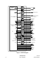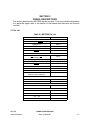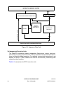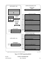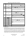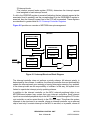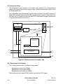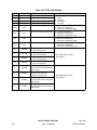
1
Freescale Semiconductor
MPC509UM/AD
MPC500 Family
MPC509
User’s Manual
© Freescale Semiconductor, Inc., 2004. All rights reserved.
How to Reach Us:
Home Page:
www.freescale.com
E-mail:
[email protected]
USA/Europe or Locations Not Listed:
Freescale Semiconductor
Technical Information Center, CH370
1300 N. Alma School Road
Chandler, Arizona 85224
+1-800-521-6274 or +1-480-768-2130
[email protected]
Europe, Middle East, and Africa:
Freescale Halbleiter Deutschland GmbH
Technical Information Center
Schatzbogen 7
81829 Muenchen, Germany
+44 1296 380 456 (English)
+46 8 52200080 (English)
+49 89 92103 559 (German)
+33 1 69 35 48 48 (French)
[email protected]
Japan:
Freescale Semiconductor Japan Ltd.
Headquarters
ARCO Tower 15F
1-8-1, Shimo-Meguro, Meguro-ku,
Tokyo 153-0064
Japan
0120 191014 or +81 3 5437 9125
[email protected]
Asia/Pacific:
Freescale Semiconductor Hong Kong Ltd.
Technical Information Center
2 Dai King Street
Tai Po Industrial Estate
Tai Po, N.T., Hong Kong
+800 2666 8080
[email protected]
For Literature Requests Only:
Freescale Semiconductor Literature Distribution Center
P.O. Box 5405
Denver, Colorado 80217
1-800-441-2447 or 303-675-2140
Fax: 303-675-2150
[email protected]
Information in this document is provided solely to enable system and software
implementers to use Freescale Semiconductor products. There are no express or
implied copyright licenses granted hereunder to design or fabricate any integrated
circuits or integrated circuits based on the information in this document.
Freescale Semiconductor reserves the right to make changes without further notice to
any products herein. Freescale Semiconductor makes no warranty, representation or
guarantee regarding the suitability of its products for any particular purpose, nor does
Freescale Semiconductor assume any liability arising out of the application or use of
any product or circuit, and specifically disclaims any and all liability, including without
limitation consequential or incidental damages. “Typical” parameters which may be
provided in Freescale Semiconductor data sheets and/or specifications can and do
vary in different applications and actual performance may vary over time. All operating
parameters, including “Typicals” must be validated for each customer application by
customer’s technical experts. Freescale Semiconductor does not convey any license
under its patent rights nor the rights of others. Freescale Semiconductor products are
not designed, intended, or authorized for use as components in systems intended for
surgical implant into the body, or other applications intended to support or sustain life,
or for any other application in which the failure of the Freescale Semiconductor product
could create a situation where personal injury or death may occur. Should Buyer
purchase or use Freescale Semiconductor products for any such unintended or
unauthorized application, Buyer shall indemnify and hold Freescale Semiconductor
and its officers, employees, subsidiaries, affiliates, and distributors harmless against all
claims, costs, damages, and expenses, and reasonable attorney fees arising out of,
directly or indirectly, any claim of personal injury or death associated with such
unintended or unauthorized use, even if such claim alleges that Freescale
Semiconductor was negligent regarding the design or manufacture of the part.
Paragraph
Number
TABLE OF CONTENTS
Page
Number
PREFACE
Section 1
INTRODUCTION
1.1 Features . . . . . . . . . . . . . . . . . . . . . . . . . . . . . . . . . . . . . . . . . . . . . . . . . . . . . . . . . . . . . . . . . . . 1-1
1.2 Block Diagram . . . . . . . . . . . . . . . . . . . . . . . . . . . . . . . . . . . . . . . . . . . . . . . . . . . . . . . . . . . . . . 1-2
1.3 Pin Connections . . . . . . . . . . . . . . . . . . . . . . . . . . . . . . . . . . . . . . . . . . . . . . . . . . . . . . . . . . . . . 1-3
1.4 Memory Map . . . . . . . . . . . . . . . . . . . . . . . . . . . . . . . . . . . . . . . . . . . . . . . . . . . . . . . . . . . . . . . 1-5
Section 2
SIGNAL DESCRIPTIONS
2.1 Pin List . . . . . . . . . . . . . . . . . . . . . . . . . . . . . . . . . . . . . . . . . . . . . . . . . . . . . . . . . . . . . . . . . . . . 2-1
2.2 Pin Characteristics . . . . . . . . . . . . . . . . . . . . . . . . . . . . . . . . . . . . . . . . . . . . . . . . . . . . . . . . . . . 2-2
2.3 Power Connections . . . . . . . . . . . . . . . . . . . . . . . . . . . . . . . . . . . . . . . . . . . . . . . . . . . . . . . . . . 2-3
2.4 Pins with Internal Pull-Ups and Pulldowns. . . . . . . . . . . . . . . . . . . . . . . . . . . . . . . . . . . . . . . . . 2-3
2.5 Signal Descriptions . . . . . . . . . . . . . . . . . . . . . . . . . . . . . . . . . . . . . . . . . . . . . . . . . . . . . . . . . . 2-4
2.5.1 Bus Arbitration and Reservation Support Signals . . . . . . . . . . . . . . . . . . . . . . . . . . . . . . 2-6
2.5.1.1 Bus Request (BR). . . . . . . . . . . . . . . . . . . . . . . . . . . . . . . . . . . . . . . . . . . . . . . . . . . 2-6
2.5.1.2 Bus Grant (BG). . . . . . . . . . . . . . . . . . . . . . . . . . . . . . . . . . . . . . . . . . . . . . . . . . . . . 2-7
2.5.1.3 Bus Busy (BB) . . . . . . . . . . . . . . . . . . . . . . . . . . . . . . . . . . . . . . . . . . . . . . . . . . . . . 2-8
2.5.1.4 Cancel Reservation (CR) . . . . . . . . . . . . . . . . . . . . . . . . . . . . . . . . . . . . . . . . . . . . . 2-8
2.5.2 Address Phase Signals . . . . . . . . . . . . . . . . . . . . . . . . . . . . . . . . . . . . . . . . . . . . . . . . . . 2-8
2.5.2.1 Address Bus (ADDR[0:29]). . . . . . . . . . . . . . . . . . . . . . . . . . . . . . . . . . . . . . . . . . . . 2-9
2.5.2.2 Write/Read (WR) . . . . . . . . . . . . . . . . . . . . . . . . . . . . . . . . . . . . . . . . . . . . . . . . . . . 2-9
2.5.2.3 Burst Indicator (BURST). . . . . . . . . . . . . . . . . . . . . . . . . . . . . . . . . . . . . . . . . . . . . . 2-9
2.5.2.4 Byte Enables (BE[0:3]) . . . . . . . . . . . . . . . . . . . . . . . . . . . . . . . . . . . . . . . . . . . . . . 2-10
2.5.2.5 Transfer Start (TS) . . . . . . . . . . . . . . . . . . . . . . . . . . . . . . . . . . . . . . . . . . . . . . . . . 2-10
2.5.2.6 Address Acknowledge (AACK). . . . . . . . . . . . . . . . . . . . . . . . . . . . . . . . . . . . . . . . 2-10
2.5.2.7 Burst Inhibit (BI) . . . . . . . . . . . . . . . . . . . . . . . . . . . . . . . . . . . . . . . . . . . . . . . . . . . 2-11
2.5.2.8 Address Retry (ARETRY) . . . . . . . . . . . . . . . . . . . . . . . . . . . . . . . . . . . . . . . . . . . . 2-12
2.5.2.9 Address Type (AT[0:1]) . . . . . . . . . . . . . . . . . . . . . . . . . . . . . . . . . . . . . . . . . . . . . 2-12
2.5.2.10 Cycle Types (CT[0:3]). . . . . . . . . . . . . . . . . . . . . . . . . . . . . . . . . . . . . . . . . . . . . . 2-13
2.5.3 Data Phase Signals . . . . . . . . . . . . . . . . . . . . . . . . . . . . . . . . . . . . . . . . . . . . . . . . . . . . 2-13
2.5.3.1 Data Bus (DATA[0:31]). . . . . . . . . . . . . . . . . . . . . . . . . . . . . . . . . . . . . . . . . . . . . . 2-13
2.5.3.2 Burst Data in Progress (BDIP) . . . . . . . . . . . . . . . . . . . . . . . . . . . . . . . . . . . . . . . . 2-14
2.5.3.3 Transfer Acknowledge (TA) . . . . . . . . . . . . . . . . . . . . . . . . . . . . . . . . . . . . . . . . . . 2-14
2.5.3.4 Transfer Error Acknowledge (TEA) . . . . . . . . . . . . . . . . . . . . . . . . . . . . . . . . . . . . 2-15
2.5.3.5 Data Strobe (DS) . . . . . . . . . . . . . . . . . . . . . . . . . . . . . . . . . . . . . . . . . . . . . . . . . . 2-15
2.5.4 Development Support Signals . . . . . . . . . . . . . . . . . . . . . . . . . . . . . . . . . . . . . . . . . . . . 2-16
2.5.4.1 Development Port Serial Data Out (DSDO) . . . . . . . . . . . . . . . . . . . . . . . . . . . . . . 2-16
2.5.4.2 Development Port Serial Data In (DSDI) . . . . . . . . . . . . . . . . . . . . . . . . . . . . . . . . 2-16
MPC509
USER’S MANUAL
TABLE OF CONTENTS
Rev. 15 June 1998
iii
Page
Number
Paragraph
Number
2.5.4.3 Development Port Serial Clock Input (DSCK) . . . . . . . . . . . . . . . . . . . . . . . . . . . . 2-16
2.5.4.4 Instruction Fetch Visibility Signals (VF[0:2]) . . . . . . . . . . . . . . . . . . . . . . . . . . . . . . 2-17
2.5.4.5 Instruction Flush Count (VFLS[0:1]) . . . . . . . . . . . . . . . . . . . . . . . . . . . . . . . . . . . . 2-17
2.5.4.6 Watchpoints (WP[0:5]) . . . . . . . . . . . . . . . . . . . . . . . . . . . . . . . . . . . . . . . . . . . . . . 2-17
2.5.5 Chip-Select Signals . . . . . . . . . . . . . . . . . . . . . . . . . . . . . . . . . . . . . . . . . . . . . . . . . . . . 2-17
2.5.5.1 Chip Select for System Boot Memory (CSBOOT) . . . . . . . . . . . . . . . . . . . . . . . . . 2-17
2.5.5.2 Chip Selects for External Memory (CS[0:11]). . . . . . . . . . . . . . . . . . . . . . . . . . . . . 2-18
2.5.6 Clock Signals . . . . . . . . . . . . . . . . . . . . . . . . . . . . . . . . . . . . . . . . . . . . . . . . . . . . . . . . . 2-18
2.5.6.1 Clock Output (CLKOUT). . . . . . . . . . . . . . . . . . . . . . . . . . . . . . . . . . . . . . . . . . . . . 2-18
2.5.6.2 Engineering Clock Output (ECROUT) . . . . . . . . . . . . . . . . . . . . . . . . . . . . . . . . . . 2-19
2.5.6.3 Crystal Oscillator Connections (EXTAL, XTAL) . . . . . . . . . . . . . . . . . . . . . . . . . . . 2-19
2.5.6.4 External Filter Capacitor Pins (XFCP, XFCN) . . . . . . . . . . . . . . . . . . . . . . . . . . . . 2-19
2.5.6.5 Clock Mode (MODCLK) . . . . . . . . . . . . . . . . . . . . . . . . . . . . . . . . . . . . . . . . . . . . . 2-19
2.5.6.6 Phase-Locked Loop Lock Signal (PLLL) . . . . . . . . . . . . . . . . . . . . . . . . . . . . . . . . 2-19
2.5.6.7 Power-Down Wake-Up (PDWU). . . . . . . . . . . . . . . . . . . . . . . . . . . . . . . . . . . . . . . 2-19
2.5.7 Reset Signals . . . . . . . . . . . . . . . . . . . . . . . . . . . . . . . . . . . . . . . . . . . . . . . . . . . . . . . . . 2-20
2.5.7.1 Reset (RESET). . . . . . . . . . . . . . . . . . . . . . . . . . . . . . . . . . . . . . . . . . . . . . . . . . . . 2-20
2.5.7.2 Reset Output (RESETOUT) . . . . . . . . . . . . . . . . . . . . . . . . . . . . . . . . . . . . . . . . . . 2-20
2.5.8 SIU General-Purpose Input/Output Signals . . . . . . . . . . . . . . . . . . . . . . . . . . . . . . . . . . 2-20
2.5.8.1 Ports A and B (PA[0:7], PB[0:7]) . . . . . . . . . . . . . . . . . . . . . . . . . . . . . . . . . . . . . . 2-20
2.5.8.2 Ports I, J, K, and L (PI[0:7], PJ[0:7], PK[0:7], PL[2:7] . . . . . . . . . . . . . . . . . . . . . . . 2-21
2.5.8.3 Port M (PM[3:7]) . . . . . . . . . . . . . . . . . . . . . . . . . . . . . . . . . . . . . . . . . . . . . . . . . . . 2-21
2.5.9 Interrupts and Port Q Signals . . . . . . . . . . . . . . . . . . . . . . . . . . . . . . . . . . . . . . . . . . . . . 2-21
2.5.9.1 Interrupt Requests (IRQ[0:6]) . . . . . . . . . . . . . . . . . . . . . . . . . . . . . . . . . . . . . . . . . 2-21
2.5.9.2 Port Q (PQ[0:6]) . . . . . . . . . . . . . . . . . . . . . . . . . . . . . . . . . . . . . . . . . . . . . . . . . . . 2-22
2.5.10 JTAG Interface Signals. . . . . . . . . . . . . . . . . . . . . . . . . . . . . . . . . . . . . . . . . . . . . . . . . 2-22
2.5.10.1 Test Data Input (TDI) . . . . . . . . . . . . . . . . . . . . . . . . . . . . . . . . . . . . . . . . . . . . . . 2-22
2.5.10.2 Test Data Output (TDO) . . . . . . . . . . . . . . . . . . . . . . . . . . . . . . . . . . . . . . . . . . . . 2-22
2.5.10.3 Test Mode Select (TMS). . . . . . . . . . . . . . . . . . . . . . . . . . . . . . . . . . . . . . . . . . . . 2-22
2.5.10.4 Test Clock (TCK) . . . . . . . . . . . . . . . . . . . . . . . . . . . . . . . . . . . . . . . . . . . . . . . . . 2-22
2.5.10.5 Test Reset (TRST) . . . . . . . . . . . . . . . . . . . . . . . . . . . . . . . . . . . . . . . . . . . . . . . . 2-23
Section 3
CENTRAL PROCESSING UNIT
3.1 RCPU Features . . . . . . . . . . . . . . . . . . . . . . . . . . . . . . . . . . . . . . . . . . . . . . . . . . . . . . . . . . . . . 3-1
3.2 RCPU Block Diagram. . . . . . . . . . . . . . . . . . . . . . . . . . . . . . . . . . . . . . . . . . . . . . . . . . . . . . . . . 3-2
3.3 Instruction Sequencer . . . . . . . . . . . . . . . . . . . . . . . . . . . . . . . . . . . . . . . . . . . . . . . . . . . . . . . . 3-3
3.4 Independent Execution Units . . . . . . . . . . . . . . . . . . . . . . . . . . . . . . . . . . . . . . . . . . . . . . . . . . . 3-4
3.4.1 Branch Processing Unit (BPU) . . . . . . . . . . . . . . . . . . . . . . . . . . . . . . . . . . . . . . . . . . . . . 3-5
3.4.2 Integer Unit (IU) . . . . . . . . . . . . . . . . . . . . . . . . . . . . . . . . . . . . . . . . . . . . . . . . . . . . . . . . 3-5
3.4.3 Load/Store Unit (LSU) . . . . . . . . . . . . . . . . . . . . . . . . . . . . . . . . . . . . . . . . . . . . . . . . . . . 3-6
3.4.4 Floating-Point Unit (FPU) . . . . . . . . . . . . . . . . . . . . . . . . . . . . . . . . . . . . . . . . . . . . . . . . . 3-6
3.5 Levels of the PowerPC Architecture . . . . . . . . . . . . . . . . . . . . . . . . . . . . . . . . . . . . . . . . . . . . . 3-7
TABLE OF CONTENTS
iv
Rev. 15 June 1998
MPC509
USER’S MANUAL
Page
Number
Paragraph
Number
3.6 RCPU Programming Model . . . . . . . . . . . . . . . . . . . . . . . . . . . . . . . . . . . . . . . . . . . . . . . . . . . . 3-7
3.7 PowerPC UISA Register Set . . . . . . . . . . . . . . . . . . . . . . . . . . . . . . . . . . . . . . . . . . . . . . . . . . 3-10
3.7.1 General-Purpose Registers (GPRs) . . . . . . . . . . . . . . . . . . . . . . . . . . . . . . . . . . . . . . . . 3-10
3.7.2 Floating-Point Registers (FPRs) . . . . . . . . . . . . . . . . . . . . . . . . . . . . . . . . . . . . . . . . . . . 3-10
3.7.3 Floating-Point Status and Control Register (FPSCR). . . . . . . . . . . . . . . . . . . . . . . . . . . 3-11
3.7.4 Condition Register (CR) . . . . . . . . . . . . . . . . . . . . . . . . . . . . . . . . . . . . . . . . . . . . . . . . . 3-13
3.7.4.1 Condition Register CR0 Field Definition . . . . . . . . . . . . . . . . . . . . . . . . . . . . . . . . . 3-14
3.7.4.2 Condition Register CR1 Field Definition . . . . . . . . . . . . . . . . . . . . . . . . . . . . . . . . . 3-14
3.7.4.3 Condition Register CRn Field — Compare Instruction . . . . . . . . . . . . . . . . . . . . . . 3-15
3.7.5 Integer Exception Register (XER) . . . . . . . . . . . . . . . . . . . . . . . . . . . . . . . . . . . . . . . . . 3-15
3.7.6 Link Register (LR). . . . . . . . . . . . . . . . . . . . . . . . . . . . . . . . . . . . . . . . . . . . . . . . . . . . . . 3-16
3.7.7 Count Register (CTR) . . . . . . . . . . . . . . . . . . . . . . . . . . . . . . . . . . . . . . . . . . . . . . . . . . . 3-17
3.8 PowerPC VEA Register Set — Time Base . . . . . . . . . . . . . . . . . . . . . . . . . . . . . . . . . . . . . . . 3-17
3.9 PowerPC OEA Register Set. . . . . . . . . . . . . . . . . . . . . . . . . . . . . . . . . . . . . . . . . . . . . . . . . . . 3-18
3.9.1 Machine State Register (MSR) . . . . . . . . . . . . . . . . . . . . . . . . . . . . . . . . . . . . . . . . . . . . 3-18
3.9.2 DAE/Source Instruction Service Register (DSISR) . . . . . . . . . . . . . . . . . . . . . . . . . . . . 3-19
3.9.3 Data Address Register (DAR) . . . . . . . . . . . . . . . . . . . . . . . . . . . . . . . . . . . . . . . . . . . . 3-20
3.9.4 Time Base Facility (TB) — OEA . . . . . . . . . . . . . . . . . . . . . . . . . . . . . . . . . . . . . . . . . . . 3-20
3.9.5 Decrementer Register (DEC) . . . . . . . . . . . . . . . . . . . . . . . . . . . . . . . . . . . . . . . . . . . . . 3-20
3.9.6 Machine Status Save/Restore Register 0 (SRR0) . . . . . . . . . . . . . . . . . . . . . . . . . . . . . 3-21
3.9.7 Machine Status Save/Restore Register 1 (SRR1) . . . . . . . . . . . . . . . . . . . . . . . . . . . . . 3-22
3.9.8 General SPRs (SPRG0–SPRG3) . . . . . . . . . . . . . . . . . . . . . . . . . . . . . . . . . . . . . . . . . . 3-22
3.9.9 Processor Version Register (PVR) . . . . . . . . . . . . . . . . . . . . . . . . . . . . . . . . . . . . . . . . . 3-22
3.9.10 Implementation-Specific SPRs . . . . . . . . . . . . . . . . . . . . . . . . . . . . . . . . . . . . . . . . . . . 3-23
3.9.10.1 EIE, EID, and NRI Special-Purpose Registers . . . . . . . . . . . . . . . . . . . . . . . . . . . 3-23
3.9.10.2 Instruction-Cache Control Registers. . . . . . . . . . . . . . . . . . . . . . . . . . . . . . . . . . . 3-23
3.9.10.3 Development Support Registers. . . . . . . . . . . . . . . . . . . . . . . . . . . . . . . . . . . . . . 3-24
3.9.10.4 Floating-Point Exception Cause Register (FPECR) . . . . . . . . . . . . . . . . . . . . . . . 3-24
3.10 Instruction Set . . . . . . . . . . . . . . . . . . . . . . . . . . . . . . . . . . . . . . . . . . . . . . . . . . . . . . . . . . . . 3-24
3.10.1 Instruction Set Summary . . . . . . . . . . . . . . . . . . . . . . . . . . . . . . . . . . . . . . . . . . . . . . . 3-26
3.10.2 Recommended Simplified Mnemonics . . . . . . . . . . . . . . . . . . . . . . . . . . . . . . . . . . . . . 3-30
3.10.3 Calculating Effective Addresses . . . . . . . . . . . . . . . . . . . . . . . . . . . . . . . . . . . . . . . . . . 3-30
3.11 Exception Model. . . . . . . . . . . . . . . . . . . . . . . . . . . . . . . . . . . . . . . . . . . . . . . . . . . . . . . . . . . 3-31
3.11.1 Exception Classes . . . . . . . . . . . . . . . . . . . . . . . . . . . . . . . . . . . . . . . . . . . . . . . . . . . . 3-31
3.11.2 Ordered Exceptions . . . . . . . . . . . . . . . . . . . . . . . . . . . . . . . . . . . . . . . . . . . . . . . . . . . 3-31
3.11.3 Unordered Exceptions . . . . . . . . . . . . . . . . . . . . . . . . . . . . . . . . . . . . . . . . . . . . . . . . . 3-31
3.11.4 Precise Exceptions . . . . . . . . . . . . . . . . . . . . . . . . . . . . . . . . . . . . . . . . . . . . . . . . . . . . 3-32
3.11.5 Exception Vector Table . . . . . . . . . . . . . . . . . . . . . . . . . . . . . . . . . . . . . . . . . . . . . . . . 3-32
3.12 Instruction Timing. . . . . . . . . . . . . . . . . . . . . . . . . . . . . . . . . . . . . . . . . . . . . . . . . . . . . . . . . . 3-33
MPC509
USER’S MANUAL
TABLE OF CONTENTS
Rev. 15 June 1998
v
Page
Number
Paragraph
Number
Section 4
INSTRUCTION CACHE
4.1 Instruction Cache Features . . . . . . . . . . . . . . . . . . . . . . . . . . . . . . . . . . . . . . . . . . . . . . . . . . . . 4-1
4.2 Instruction Cache Organization . . . . . . . . . . . . . . . . . . . . . . . . . . . . . . . . . . . . . . . . . . . . . . . . . 4-2
4.3 Instruction Cache Programming Model . . . . . . . . . . . . . . . . . . . . . . . . . . . . . . . . . . . . . . . . . . . 4-3
4.4 Cache Operation . . . . . . . . . . . . . . . . . . . . . . . . . . . . . . . . . . . . . . . . . . . . . . . . . . . . . . . . . . . . 4-5
4.5 Cache Commands . . . . . . . . . . . . . . . . . . . . . . . . . . . . . . . . . . . . . . . . . . . . . . . . . . . . . . . . . . . 4-6
Section 5
SYSTEM INTERFACE UNIT
5.1 SIU Block Diagram. . . . . . . . . . . . . . . . . . . . . . . . . . . . . . . . . . . . . . . . . . . . . . . . . . . . . . . . . . . 5-1
5.2 SIU Address Map . . . . . . . . . . . . . . . . . . . . . . . . . . . . . . . . . . . . . . . . . . . . . . . . . . . . . . . . . . . . 5-2
5.3 SIU Module Configuration . . . . . . . . . . . . . . . . . . . . . . . . . . . . . . . . . . . . . . . . . . . . . . . . . . . . . 5-4
5.3.1 SIU Module Configuration Register . . . . . . . . . . . . . . . . . . . . . . . . . . . . . . . . . . . . . . . . . 5-4
5.3.2 Memory Mapping Register . . . . . . . . . . . . . . . . . . . . . . . . . . . . . . . . . . . . . . . . . . . . . . . . 5-6
5.3.3 Internal Module Select Logic . . . . . . . . . . . . . . . . . . . . . . . . . . . . . . . . . . . . . . . . . . . . . . 5-7
5.3.3.1 Memory Block Mapping . . . . . . . . . . . . . . . . . . . . . . . . . . . . . . . . . . . . . . . . . . . . . . 5-8
5.3.3.2 Accesses to Unimplemented Internal Memory Locations. . . . . . . . . . . . . . . . . . . . . 5-9
5.3.3.3 Control Register Block . . . . . . . . . . . . . . . . . . . . . . . . . . . . . . . . . . . . . . . . . . . . . . . 5-9
5.3.3.4 Internal Memory Mapping Field (LMEMBASE). . . . . . . . . . . . . . . . . . . . . . . . . . . . 5-10
5.3.3.5 Memory Mapping Conflicts . . . . . . . . . . . . . . . . . . . . . . . . . . . . . . . . . . . . . . . . . . . 5-10
5.3.4 Internal Cross-Bus Accesses . . . . . . . . . . . . . . . . . . . . . . . . . . . . . . . . . . . . . . . . . . . . . 5-10
5.3.5 Response to Freeze Assertion . . . . . . . . . . . . . . . . . . . . . . . . . . . . . . . . . . . . . . . . . . . . 5-11
5.3.5.1 Effects of Freeze and Debug Mode on the Bus Monitor. . . . . . . . . . . . . . . . . . . . . 5-11
5.3.5.2 Effects of Freeze on the Programmable Interrupt Timer (PIT) . . . . . . . . . . . . . . . . 5-11
5.3.5.3 Effects of Freeze on the Decrementer . . . . . . . . . . . . . . . . . . . . . . . . . . . . . . . . . . 5-12
5.3.5.4 Effects of Freeze on Register Lock Bits . . . . . . . . . . . . . . . . . . . . . . . . . . . . . . . . . 5-12
5.4 External Bus Interface . . . . . . . . . . . . . . . . . . . . . . . . . . . . . . . . . . . . . . . . . . . . . . . . . . . . . . . 5-12
5.4.1 Features . . . . . . . . . . . . . . . . . . . . . . . . . . . . . . . . . . . . . . . . . . . . . . . . . . . . . . . . . . . . . 5-12
5.4.2 External Bus Signals . . . . . . . . . . . . . . . . . . . . . . . . . . . . . . . . . . . . . . . . . . . . . . . . . . . 5-12
5.4.3 Basic Bus Cycle . . . . . . . . . . . . . . . . . . . . . . . . . . . . . . . . . . . . . . . . . . . . . . . . . . . . . . . 5-15
5.4.3.1 Read Cycle Flow . . . . . . . . . . . . . . . . . . . . . . . . . . . . . . . . . . . . . . . . . . . . . . . . . . 5-15
5.4.3.2 Write Cycle Flow. . . . . . . . . . . . . . . . . . . . . . . . . . . . . . . . . . . . . . . . . . . . . . . . . . . 5-17
5.4.4 Basic Pipeline . . . . . . . . . . . . . . . . . . . . . . . . . . . . . . . . . . . . . . . . . . . . . . . . . . . . . . . . . 5-18
5.4.5 Bus Cycle Phases . . . . . . . . . . . . . . . . . . . . . . . . . . . . . . . . . . . . . . . . . . . . . . . . . . . . . 5-20
5.4.5.1 Arbitration Phase . . . . . . . . . . . . . . . . . . . . . . . . . . . . . . . . . . . . . . . . . . . . . . . . . . 5-20
5.4.5.2 Address Phase . . . . . . . . . . . . . . . . . . . . . . . . . . . . . . . . . . . . . . . . . . . . . . . . . . . . 5-20
5.4.5.3 Data Phase. . . . . . . . . . . . . . . . . . . . . . . . . . . . . . . . . . . . . . . . . . . . . . . . . . . . . . . 5-21
5.4.6 Burst Cycles . . . . . . . . . . . . . . . . . . . . . . . . . . . . . . . . . . . . . . . . . . . . . . . . . . . . . . . . . . 5-22
5.4.6.1 Termination of Burst Cycles . . . . . . . . . . . . . . . . . . . . . . . . . . . . . . . . . . . . . . . . . . 5-23
5.4.6.2 Burst Inhibit Cycles. . . . . . . . . . . . . . . . . . . . . . . . . . . . . . . . . . . . . . . . . . . . . . . . . 5-23
5.4.7 Decomposed Cycles and Address Wrapping . . . . . . . . . . . . . . . . . . . . . . . . . . . . . . . . . 5-24
5.4.8 Preventing Speculative Loads . . . . . . . . . . . . . . . . . . . . . . . . . . . . . . . . . . . . . . . . . . . . 5-25
TABLE OF CONTENTS
vi
Rev. 15 June 1998
MPC509
USER’S MANUAL
Page
Number
Paragraph
Number
5.4.9 Accesses to 16-Bit Ports . . . . . . . . . . . . . . . . . . . . . . . . . . . . . . . . . . . . . . . . . . . . . . . . 5-27
5.4.10 Address Retry. . . . . . . . . . . . . . . . . . . . . . . . . . . . . . . . . . . . . . . . . . . . . . . . . . . . . . . . 5-28
5.4.11 Transfer Error Acknowledge Cycles . . . . . . . . . . . . . . . . . . . . . . . . . . . . . . . . . . . . . . . 5-28
5.4.12 Cycle Types . . . . . . . . . . . . . . . . . . . . . . . . . . . . . . . . . . . . . . . . . . . . . . . . . . . . . . . . . 5-29
5.4.13 Show Cycles . . . . . . . . . . . . . . . . . . . . . . . . . . . . . . . . . . . . . . . . . . . . . . . . . . . . . . . . . 5-30
5.4.14 Storage Reservation Support . . . . . . . . . . . . . . . . . . . . . . . . . . . . . . . . . . . . . . . . . . . . 5-31
5.4.14.1 PowerPC Architecture Reservation Requirements. . . . . . . . . . . . . . . . . . . . . . . . 5-32
5.4.14.2 E-bus Storage Reservation Implementation. . . . . . . . . . . . . . . . . . . . . . . . . . . . . 5-33
5.4.14.3 Reservation Storage Signals . . . . . . . . . . . . . . . . . . . . . . . . . . . . . . . . . . . . . . . . 5-33
5.5 Chip Selects . . . . . . . . . . . . . . . . . . . . . . . . . . . . . . . . . . . . . . . . . . . . . . . . . . . . . . . . . . . . . . . 5-34
5.5.1 Chip-Select Features . . . . . . . . . . . . . . . . . . . . . . . . . . . . . . . . . . . . . . . . . . . . . . . . . . . 5-35
5.5.2 Chip-Select Block Diagram. . . . . . . . . . . . . . . . . . . . . . . . . . . . . . . . . . . . . . . . . . . . . . . 5-35
5.5.3 Chip-Select Pins . . . . . . . . . . . . . . . . . . . . . . . . . . . . . . . . . . . . . . . . . . . . . . . . . . . . . . . 5-36
5.5.4 Chip-Select Registers and Address Map . . . . . . . . . . . . . . . . . . . . . . . . . . . . . . . . . . . . 5-37
5.5.4.1 Chip-Select Base Address Registers . . . . . . . . . . . . . . . . . . . . . . . . . . . . . . . . . . . 5-39
5.5.4.2 Chip-Select Option Registers . . . . . . . . . . . . . . . . . . . . . . . . . . . . . . . . . . . . . . . . . 5-40
5.5.5 Chip-Select Regions . . . . . . . . . . . . . . . . . . . . . . . . . . . . . . . . . . . . . . . . . . . . . . . . . . . . 5-44
5.5.6 Multi-Level Protection . . . . . . . . . . . . . . . . . . . . . . . . . . . . . . . . . . . . . . . . . . . . . . . . . . . 5-46
5.5.6.1 Main Block and Sub-Block Pairings . . . . . . . . . . . . . . . . . . . . . . . . . . . . . . . . . . . . 5-46
5.5.6.2 Programming the Sub-Block Option Register. . . . . . . . . . . . . . . . . . . . . . . . . . . . . 5-47
5.5.6.3 Multi-Level Protection for CSBOOT . . . . . . . . . . . . . . . . . . . . . . . . . . . . . . . . . . . . 5-47
5.5.7 Access Protection. . . . . . . . . . . . . . . . . . . . . . . . . . . . . . . . . . . . . . . . . . . . . . . . . . . . . . 5-48
5.5.7.1 Supervisor Space Protection . . . . . . . . . . . . . . . . . . . . . . . . . . . . . . . . . . . . . . . . . 5-48
5.5.7.2 Data Space Protection . . . . . . . . . . . . . . . . . . . . . . . . . . . . . . . . . . . . . . . . . . . . . . 5-48
5.5.7.3 Write Protection . . . . . . . . . . . . . . . . . . . . . . . . . . . . . . . . . . . . . . . . . . . . . . . . . . . 5-48
5.5.8 Cache Inhibit Control . . . . . . . . . . . . . . . . . . . . . . . . . . . . . . . . . . . . . . . . . . . . . . . . . . . 5-49
5.5.9 Handshaking Control . . . . . . . . . . . . . . . . . . . . . . . . . . . . . . . . . . . . . . . . . . . . . . . . . . . 5-49
5.5.10 Wait State Control . . . . . . . . . . . . . . . . . . . . . . . . . . . . . . . . . . . . . . . . . . . . . . . . . . . . 5-49
5.5.11 Port Size . . . . . . . . . . . . . . . . . . . . . . . . . . . . . . . . . . . . . . . . . . . . . . . . . . . . . . . . . . . . 5-50
5.5.12 Chip-Select Pin Control . . . . . . . . . . . . . . . . . . . . . . . . . . . . . . . . . . . . . . . . . . . . . . . . 5-50
5.5.12.1 Pin Configuration . . . . . . . . . . . . . . . . . . . . . . . . . . . . . . . . . . . . . . . . . . . . . . . . . 5-51
5.5.12.2 Byte Enable Control . . . . . . . . . . . . . . . . . . . . . . . . . . . . . . . . . . . . . . . . . . . . . . . 5-51
5.5.12.3 Region Control . . . . . . . . . . . . . . . . . . . . . . . . . . . . . . . . . . . . . . . . . . . . . . . . . . . 5-51
5.5.13 Interface Types . . . . . . . . . . . . . . . . . . . . . . . . . . . . . . . . . . . . . . . . . . . . . . . . . . . . . . . 5-52
5.5.13.1 Interface Type Descriptions . . . . . . . . . . . . . . . . . . . . . . . . . . . . . . . . . . . . . . . . . 5-53
5.5.13.2 Turn-Off Times for Different Interface Types . . . . . . . . . . . . . . . . . . . . . . . . . . . . 5-54
5.5.13.3 Interface Type and BI Generation . . . . . . . . . . . . . . . . . . . . . . . . . . . . . . . . . . . . 5-55
5.5.14 Chip-Select Operation Flowchart . . . . . . . . . . . . . . . . . . . . . . . . . . . . . . . . . . . . . . . . . 5-55
5.5.15 Pipe Tracking . . . . . . . . . . . . . . . . . . . . . . . . . . . . . . . . . . . . . . . . . . . . . . . . . . . . . . . . 5-56
5.5.15.1 Pipelined Accesses to the Same Region . . . . . . . . . . . . . . . . . . . . . . . . . . . . . . . 5-57
5.5.15.2 Pipelined Accesses to Different Regions . . . . . . . . . . . . . . . . . . . . . . . . . . . . . . . 5-57
5.5.16 Chip-Select Timing Diagrams . . . . . . . . . . . . . . . . . . . . . . . . . . . . . . . . . . . . . . . . . . . . 5-59
5.5.16.1 Asynchronous Interface . . . . . . . . . . . . . . . . . . . . . . . . . . . . . . . . . . . . . . . . . . . . 5-59
MPC509
USER’S MANUAL
TABLE OF CONTENTS
Rev. 15 June 1998
vii
Page
Number
Paragraph
Number
5.5.16.2 Asynchronous Interface with Latch Enable . . . . . . . . . . . . . . . . . . . . . . . . . . . . . 5-60
5.5.16.3 Synchronous Interface with Asynchronous OE . . . . . . . . . . . . . . . . . . . . . . . . . . 5-60
5.5.16.4 Synchronous Interface with Early Synchronous OE. . . . . . . . . . . . . . . . . . . . . . . 5-61
5.5.16.5 Synchronous Interface with Synchronous OE, Early Overlap . . . . . . . . . . . . . . . 5-62
5.5.16.6 Synchronous Burst Interface . . . . . . . . . . . . . . . . . . . . . . . . . . . . . . . . . . . . . . . . 5-63
5.5.17 Burst Handling . . . . . . . . . . . . . . . . . . . . . . . . . . . . . . . . . . . . . . . . . . . . . . . . . . . . . . . 5-66
5.5.18 Chip-Select Reset Operation . . . . . . . . . . . . . . . . . . . . . . . . . . . . . . . . . . . . . . . . . . . . 5-67
5.6 Clock Submodule . . . . . . . . . . . . . . . . . . . . . . . . . . . . . . . . . . . . . . . . . . . . . . . . . . . . . . . . . . . 5-67
5.6.1 Clock Submodule Signal Descriptions . . . . . . . . . . . . . . . . . . . . . . . . . . . . . . . . . . . . . . 5-70
5.6.2 Clock Power Supplies. . . . . . . . . . . . . . . . . . . . . . . . . . . . . . . . . . . . . . . . . . . . . . . . . . . 5-70
5.6.3 System Clock Sources . . . . . . . . . . . . . . . . . . . . . . . . . . . . . . . . . . . . . . . . . . . . . . . . . . 5-71
5.6.4 Phase-Locked Loop . . . . . . . . . . . . . . . . . . . . . . . . . . . . . . . . . . . . . . . . . . . . . . . . . . . . 5-71
5.6.4.1 Crystal Oscillator . . . . . . . . . . . . . . . . . . . . . . . . . . . . . . . . . . . . . . . . . . . . . . . . . . 5-72
5.6.4.2 Phase Detector. . . . . . . . . . . . . . . . . . . . . . . . . . . . . . . . . . . . . . . . . . . . . . . . . . . . 5-73
5.6.4.3 Charge Pump and Loop Filter . . . . . . . . . . . . . . . . . . . . . . . . . . . . . . . . . . . . . . . . 5-73
5.6.4.4 VCO . . . . . . . . . . . . . . . . . . . . . . . . . . . . . . . . . . . . . . . . . . . . . . . . . . . . . . . . . . . . 5-74
5.6.4.5 Multiplication Factor Divider . . . . . . . . . . . . . . . . . . . . . . . . . . . . . . . . . . . . . . . . . . 5-74
5.6.4.6 Clock Delay . . . . . . . . . . . . . . . . . . . . . . . . . . . . . . . . . . . . . . . . . . . . . . . . . . . . . . 5-74
5.6.5 CLKOUT Frequency Control . . . . . . . . . . . . . . . . . . . . . . . . . . . . . . . . . . . . . . . . . . . . . 5-74
5.6.5.1 Multiplication Factor (MF) Bits . . . . . . . . . . . . . . . . . . . . . . . . . . . . . . . . . . . . . . . . 5-75
5.6.5.2 Reduced Frequency Divider (RFD[0:3]) . . . . . . . . . . . . . . . . . . . . . . . . . . . . . . . . . 5-77
5.6.6 Low-Power Modes . . . . . . . . . . . . . . . . . . . . . . . . . . . . . . . . . . . . . . . . . . . . . . . . . . . . . 5-78
5.6.6.1 Normal Mode . . . . . . . . . . . . . . . . . . . . . . . . . . . . . . . . . . . . . . . . . . . . . . . . . . . . . 5-78
5.6.6.2 Single-Chip Mode . . . . . . . . . . . . . . . . . . . . . . . . . . . . . . . . . . . . . . . . . . . . . . . . . . 5-78
5.6.6.3 Doze Mode . . . . . . . . . . . . . . . . . . . . . . . . . . . . . . . . . . . . . . . . . . . . . . . . . . . . . . . 5-78
5.6.6.4 Sleep Mode . . . . . . . . . . . . . . . . . . . . . . . . . . . . . . . . . . . . . . . . . . . . . . . . . . . . . . 5-79
5.6.6.5 Exiting Low-Power Mode . . . . . . . . . . . . . . . . . . . . . . . . . . . . . . . . . . . . . . . . . . . . 5-79
5.6.7 System Clock Lock Bits . . . . . . . . . . . . . . . . . . . . . . . . . . . . . . . . . . . . . . . . . . . . . . . . . 5-79
5.6.8 Power-Down Wake Up . . . . . . . . . . . . . . . . . . . . . . . . . . . . . . . . . . . . . . . . . . . . . . . . . . 5-80
5.6.9 Time Base and Decrementer Support . . . . . . . . . . . . . . . . . . . . . . . . . . . . . . . . . . . . . . 5-80
5.6.9.1 Time Base and Decrementer Clock Source . . . . . . . . . . . . . . . . . . . . . . . . . . . . . . 5-81
5.6.9.2 Time Base/Decrementer and Freeze Assertion . . . . . . . . . . . . . . . . . . . . . . . . . . . 5-81
5.6.9.3 Decrementer Clock Enable (DCE) Bit . . . . . . . . . . . . . . . . . . . . . . . . . . . . . . . . . . 5-81
5.6.10 Clock Resets . . . . . . . . . . . . . . . . . . . . . . . . . . . . . . . . . . . . . . . . . . . . . . . . . . . . . . . . 5-81
5.6.10.1 Loss of PLL Lock . . . . . . . . . . . . . . . . . . . . . . . . . . . . . . . . . . . . . . . . . . . . . . . . . 5-82
5.6.10.2 Loss of Oscillator . . . . . . . . . . . . . . . . . . . . . . . . . . . . . . . . . . . . . . . . . . . . . . . . . 5-82
5.6.11 System Clock Control Register (SCCR) . . . . . . . . . . . . . . . . . . . . . . . . . . . . . . . . . . . . 5-83
5.6.12 System Clock Lock and Status Register (SCLSR) . . . . . . . . . . . . . . . . . . . . . . . . . . . . 5-84
5.7 System Protection . . . . . . . . . . . . . . . . . . . . . . . . . . . . . . . . . . . . . . . . . . . . . . . . . . . . . . . . . . 5-85
5.7.1 System Protection Features . . . . . . . . . . . . . . . . . . . . . . . . . . . . . . . . . . . . . . . . . . . . . . 5-85
5.7.2 System Protection Registers . . . . . . . . . . . . . . . . . . . . . . . . . . . . . . . . . . . . . . . . . . . . . 5-86
5.7.3 Periodic Interrupt Timer (PIT) . . . . . . . . . . . . . . . . . . . . . . . . . . . . . . . . . . . . . . . . . . . . . 5-86
5.7.3.1 PIT Clock Frequency Selection . . . . . . . . . . . . . . . . . . . . . . . . . . . . . . . . . . . . . . . 5-87
TABLE OF CONTENTS
viii
Rev. 15 June 1998
MPC509
USER’S MANUAL
Page
Number
Paragraph
Number
5.7.3.2 PIT Time-Out Period Selection. . . . . . . . . . . . . . . . . . . . . . . . . . . . . . . . . . . . . . . . 5-88
5.7.3.3 PIT Enable Bits. . . . . . . . . . . . . . . . . . . . . . . . . . . . . . . . . . . . . . . . . . . . . . . . . . . . 5-89
5.7.3.4 PIT Interrupt Request Level and Status . . . . . . . . . . . . . . . . . . . . . . . . . . . . . . . . . 5-89
5.7.3.5 Periodic Interrupt Control and Select Register . . . . . . . . . . . . . . . . . . . . . . . . . . . . 5-89
5.7.3.6 Periodic Interrupt Timer Register . . . . . . . . . . . . . . . . . . . . . . . . . . . . . . . . . . . . . . 5-90
5.7.4 Hardware Bus Monitor . . . . . . . . . . . . . . . . . . . . . . . . . . . . . . . . . . . . . . . . . . . . . . . . . . 5-90
5.7.4.1 Bus Monitor Timing. . . . . . . . . . . . . . . . . . . . . . . . . . . . . . . . . . . . . . . . . . . . . . . . . 5-91
5.7.4.2 Bus Monitor Lock . . . . . . . . . . . . . . . . . . . . . . . . . . . . . . . . . . . . . . . . . . . . . . . . . . 5-91
5.7.4.3 Bus Monitor Enable . . . . . . . . . . . . . . . . . . . . . . . . . . . . . . . . . . . . . . . . . . . . . . . . 5-91
5.7.4.4 Bus Monitor Control Register . . . . . . . . . . . . . . . . . . . . . . . . . . . . . . . . . . . . . . . . . 5-91
5.8 Reset Operation . . . . . . . . . . . . . . . . . . . . . . . . . . . . . . . . . . . . . . . . . . . . . . . . . . . . . . . . . . . . 5-92
5.8.1 Reset Sources . . . . . . . . . . . . . . . . . . . . . . . . . . . . . . . . . . . . . . . . . . . . . . . . . . . . . . . . 5-92
5.8.2 Reset Flow . . . . . . . . . . . . . . . . . . . . . . . . . . . . . . . . . . . . . . . . . . . . . . . . . . . . . . . . . . . 5-93
5.8.2.1 External Reset Request Flow . . . . . . . . . . . . . . . . . . . . . . . . . . . . . . . . . . . . . . . . . 5-93
5.8.2.2 Internal Reset Request Flow . . . . . . . . . . . . . . . . . . . . . . . . . . . . . . . . . . . . . . . . . 5-95
5.8.2.3 Reset Behavior for Different Clock Modes . . . . . . . . . . . . . . . . . . . . . . . . . . . . . . . 5-97
5.8.3 Configuration During Reset . . . . . . . . . . . . . . . . . . . . . . . . . . . . . . . . . . . . . . . . . . . . . . 5-98
5.8.3.1 Data Bus Configuration Mode . . . . . . . . . . . . . . . . . . . . . . . . . . . . . . . . . . . . . . . . 5-98
5.8.3.2 Internal Default Mode . . . . . . . . . . . . . . . . . . . . . . . . . . . . . . . . . . . . . . . . . . . . . . . 5-99
5.8.3.3 Data Bus Reset Configuration Word . . . . . . . . . . . . . . . . . . . . . . . . . . . . . . . . . . . 5-99
5.8.4 Power-On Reset . . . . . . . . . . . . . . . . . . . . . . . . . . . . . . . . . . . . . . . . . . . . . . . . . . . . . . 5-101
5.9 General-Purpose I/O . . . . . . . . . . . . . . . . . . . . . . . . . . . . . . . . . . . . . . . . . . . . . . . . . . . . . . . 5-101
5.9.1 Port Timing . . . . . . . . . . . . . . . . . . . . . . . . . . . . . . . . . . . . . . . . . . . . . . . . . . . . . . . . . . 5-102
5.9.2 Port M . . . . . . . . . . . . . . . . . . . . . . . . . . . . . . . . . . . . . . . . . . . . . . . . . . . . . . . . . . . . . . 5-103
5.9.3 Ports A and B . . . . . . . . . . . . . . . . . . . . . . . . . . . . . . . . . . . . . . . . . . . . . . . . . . . . . . . . 5-104
5.9.4 Ports I, J, K, and L . . . . . . . . . . . . . . . . . . . . . . . . . . . . . . . . . . . . . . . . . . . . . . . . . . . . 5-106
5.9.5 Port Replacement Unit (PRU) Mode . . . . . . . . . . . . . . . . . . . . . . . . . . . . . . . . . . . . . . 5-108
Section 6
PERIPHERAL CONTROL UNIT
6.1 PCU Block Diagram . . . . . . . . . . . . . . . . . . . . . . . . . . . . . . . . . . . . . . . . . . . . . . . . . . . . . . . . . . 6-1
6.2 PCU Address Map . . . . . . . . . . . . . . . . . . . . . . . . . . . . . . . . . . . . . . . . . . . . . . . . . . . . . . . . . . . 6-2
6.3 Module Configuration . . . . . . . . . . . . . . . . . . . . . . . . . . . . . . . . . . . . . . . . . . . . . . . . . . . . . . . . . 6-2
6.4 Software Watchdog . . . . . . . . . . . . . . . . . . . . . . . . . . . . . . . . . . . . . . . . . . . . . . . . . . . . . . . . . . 6-3
6.4.1 Software Watchdog Service Register . . . . . . . . . . . . . . . . . . . . . . . . . . . . . . . . . . . . . . . . 6-4
6.4.2 Software Watchdog Control Register/Timing Count . . . . . . . . . . . . . . . . . . . . . . . . . . . . . 6-4
6.4.3 Software Watchdog Register . . . . . . . . . . . . . . . . . . . . . . . . . . . . . . . . . . . . . . . . . . . . . . 6-5
6.5 Interrupt Controller . . . . . . . . . . . . . . . . . . . . . . . . . . . . . . . . . . . . . . . . . . . . . . . . . . . . . . . . . . . 6-5
6.5.1 Interrupt Controller Operation . . . . . . . . . . . . . . . . . . . . . . . . . . . . . . . . . . . . . . . . . . . . . . 6-5
6.5.2 Interrupt Sources . . . . . . . . . . . . . . . . . . . . . . . . . . . . . . . . . . . . . . . . . . . . . . . . . . . . . . . 6-7
6.5.2.1 External Interrupt Requests . . . . . . . . . . . . . . . . . . . . . . . . . . . . . . . . . . . . . . . . . . . 6-7
6.5.2.2 Periodic Interrupt Timer Interrupts . . . . . . . . . . . . . . . . . . . . . . . . . . . . . . . . . . . . . . 6-7
6.5.2.3 Interrupt Request Multiplexing . . . . . . . . . . . . . . . . . . . . . . . . . . . . . . . . . . . . . . . . . 6-7
MPC509
USER’S MANUAL
TABLE OF CONTENTS
Rev. 15 June 1998
ix
Page
Number
Paragraph
Number
6.5.3 Interrupt Controller Registers . . . . . . . . . . . . . . . . . . . . . . . . . . . . . . . . . . . . . . . . . . . . . . 6-8
6.5.3.1 Pending Interrupt Request Register . . . . . . . . . . . . . . . . . . . . . . . . . . . . . . . . . . . . . 6-9
6.5.3.2 Enabled Active Interrupt Requests Register. . . . . . . . . . . . . . . . . . . . . . . . . . . . . . . 6-9
6.5.3.3 Interrupt Enable Register . . . . . . . . . . . . . . . . . . . . . . . . . . . . . . . . . . . . . . . . . . . . . 6-9
6.5.3.4 PIT/Port Q Interrupt Levels Register . . . . . . . . . . . . . . . . . . . . . . . . . . . . . . . . . . . 6-10
6.6 Port Q. . . . . . . . . . . . . . . . . . . . . . . . . . . . . . . . . . . . . . . . . . . . . . . . . . . . . . . . . . . . . . . . . . . . 6-10
6.6.1 Port Q Edge Detect/Data Register . . . . . . . . . . . . . . . . . . . . . . . . . . . . . . . . . . . . . . . . . 6-11
6.6.2 Port Q Pin Assignment Register . . . . . . . . . . . . . . . . . . . . . . . . . . . . . . . . . . . . . . . . . . . 6-11
6.6.2.1 Port Q Pin Assignment Fields. . . . . . . . . . . . . . . . . . . . . . . . . . . . . . . . . . . . . . . . . 6-12
6.6.2.2 Port Q Edge Fields . . . . . . . . . . . . . . . . . . . . . . . . . . . . . . . . . . . . . . . . . . . . . . . . . 6-12
Section 7
STATIC RAM MODULE
7.1 Features . . . . . . . . . . . . . . . . . . . . . . . . . . . . . . . . . . . . . . . . . . . . . . . . . . . . . . . . . . . . . . . . . . . 7-1
7.2 Placement of SRAM in Memory Map . . . . . . . . . . . . . . . . . . . . . . . . . . . . . . . . . . . . . . . . . . . . . 7-1
7.3 SRAM Registers. . . . . . . . . . . . . . . . . . . . . . . . . . . . . . . . . . . . . . . . . . . . . . . . . . . . . . . . . . . . . 7-2
Section 8
DEVELOPMENT SUPPORT
8.1 Program Flow Tracking . . . . . . . . . . . . . . . . . . . . . . . . . . . . . . . . . . . . . . . . . . . . . . . . . . . . . . . 8-1
8.1.1 Indirect Change-of-Flow Cycles . . . . . . . . . . . . . . . . . . . . . . . . . . . . . . . . . . . . . . . . . . . . 8-2
8.1.1.1 Marking the Indirect Change-of-Flow Attribute . . . . . . . . . . . . . . . . . . . . . . . . . . . . . 8-3
8.1.1.2 Sequential Instructions with the Indirect Change-of-Flow Attribute . . . . . . . . . . . . . 8-3
8.1.2 Instruction Fetch Show Cycle Control . . . . . . . . . . . . . . . . . . . . . . . . . . . . . . . . . . . . . . . 8-4
8.1.3 Program Flow-Tracking Pins . . . . . . . . . . . . . . . . . . . . . . . . . . . . . . . . . . . . . . . . . . . . . . 8-4
8.1.3.1 Instruction Queue Status Pins . . . . . . . . . . . . . . . . . . . . . . . . . . . . . . . . . . . . . . . . . 8-5
8.1.3.2 History Buffer Flush Status Pins. . . . . . . . . . . . . . . . . . . . . . . . . . . . . . . . . . . . . . . . 8-6
8.1.3.3 Flow-Tracking Status Pins in Debug Mode . . . . . . . . . . . . . . . . . . . . . . . . . . . . . . . 8-6
8.1.3.4 Cycle Type, Write/Read, and Address Type Pins . . . . . . . . . . . . . . . . . . . . . . . . . . 8-7
8.1.4 External Hardware During Program Trace . . . . . . . . . . . . . . . . . . . . . . . . . . . . . . . . . . . . 8-7
8.1.4.1 Back Trace . . . . . . . . . . . . . . . . . . . . . . . . . . . . . . . . . . . . . . . . . . . . . . . . . . . . . . . . 8-8
8.1.4.2 Window Trace. . . . . . . . . . . . . . . . . . . . . . . . . . . . . . . . . . . . . . . . . . . . . . . . . . . . . . 8-8
8.1.4.3 Synchronizing the Trace Window to Internal CPU Events . . . . . . . . . . . . . . . . . . . . 8-8
8.1.4.4 Detecting the Trace Window Starting Address. . . . . . . . . . . . . . . . . . . . . . . . . . . . . 8-9
8.1.4.5 Detecting the Assertion or Negation of VSYNC . . . . . . . . . . . . . . . . . . . . . . . . . . . 8-10
8.1.4.6 Detecting the Trace Window Ending Address . . . . . . . . . . . . . . . . . . . . . . . . . . . . 8-10
8.1.5 Compress . . . . . . . . . . . . . . . . . . . . . . . . . . . . . . . . . . . . . . . . . . . . . . . . . . . . . . . . . . . . 8-11
8.2 Watchpoint and Breakpoint Support . . . . . . . . . . . . . . . . . . . . . . . . . . . . . . . . . . . . . . . . . . . . 8-11
8.2.1 Watchpoints . . . . . . . . . . . . . . . . . . . . . . . . . . . . . . . . . . . . . . . . . . . . . . . . . . . . . . . . . . 8-12
8.2.1.1 Restrictions on Watchpoint Detection. . . . . . . . . . . . . . . . . . . . . . . . . . . . . . . . . . . 8-13
8.2.1.2 Byte and Half-Word Working Modes . . . . . . . . . . . . . . . . . . . . . . . . . . . . . . . . . . . 8-13
8.2.1.3 Generating Six Compare Types . . . . . . . . . . . . . . . . . . . . . . . . . . . . . . . . . . . . . . . 8-15
8.2.1.4 I-Bus Support Detailed Description . . . . . . . . . . . . . . . . . . . . . . . . . . . . . . . . . . . . 8-15
8.2.1.5 L-Bus Support Detailed Description . . . . . . . . . . . . . . . . . . . . . . . . . . . . . . . . . . . . 8-17
TABLE OF CONTENTS
x
Rev. 15 June 1998
MPC509
USER’S MANUAL
Page
Number
Paragraph
Number
8.2.1.6 Treating Floating-Point Numbers . . . . . . . . . . . . . . . . . . . . . . . . . . . . . . . . . . . . . . 8-19
8.2.2 Internal Breakpoints . . . . . . . . . . . . . . . . . . . . . . . . . . . . . . . . . . . . . . . . . . . . . . . . . . . . 8-19
8.2.2.1 Breakpoint Counters. . . . . . . . . . . . . . . . . . . . . . . . . . . . . . . . . . . . . . . . . . . . . . . . 8-20
8.2.2.2 Trap-Enable Programming . . . . . . . . . . . . . . . . . . . . . . . . . . . . . . . . . . . . . . . . . . . 8-20
8.2.2.3 Ignore First Match. . . . . . . . . . . . . . . . . . . . . . . . . . . . . . . . . . . . . . . . . . . . . . . . . . 8-20
8.2.3 External Breakpoints . . . . . . . . . . . . . . . . . . . . . . . . . . . . . . . . . . . . . . . . . . . . . . . . . . . 8-21
8.2.4 Breakpoint Masking . . . . . . . . . . . . . . . . . . . . . . . . . . . . . . . . . . . . . . . . . . . . . . . . . . . . 8-21
8.3 Development Port . . . . . . . . . . . . . . . . . . . . . . . . . . . . . . . . . . . . . . . . . . . . . . . . . . . . . . . . . . 8-22
8.3.1 Development Port Signals . . . . . . . . . . . . . . . . . . . . . . . . . . . . . . . . . . . . . . . . . . . . . . . 8-22
8.3.1.1 Development Serial Clock . . . . . . . . . . . . . . . . . . . . . . . . . . . . . . . . . . . . . . . . . . . 8-23
8.3.1.2 Development Serial Data In . . . . . . . . . . . . . . . . . . . . . . . . . . . . . . . . . . . . . . . . . . 8-23
8.3.1.3 Development Serial Data Out. . . . . . . . . . . . . . . . . . . . . . . . . . . . . . . . . . . . . . . . . 8-24
8.3.2 Development Port Registers. . . . . . . . . . . . . . . . . . . . . . . . . . . . . . . . . . . . . . . . . . . . . . 8-24
8.3.2.1 Development Port Shift Register . . . . . . . . . . . . . . . . . . . . . . . . . . . . . . . . . . . . . . 8-25
8.3.2.2 Trap Enable Control Register . . . . . . . . . . . . . . . . . . . . . . . . . . . . . . . . . . . . . . . . . 8-25
8.3.3 Development Port Clock Mode Selection . . . . . . . . . . . . . . . . . . . . . . . . . . . . . . . . . . . . 8-25
8.3.4 Development Port Transmissions. . . . . . . . . . . . . . . . . . . . . . . . . . . . . . . . . . . . . . . . . . 8-30
8.3.5 Trap-Enable Input Transmissions. . . . . . . . . . . . . . . . . . . . . . . . . . . . . . . . . . . . . . . . . . 8-30
8.3.6 CPU Input Transmissions . . . . . . . . . . . . . . . . . . . . . . . . . . . . . . . . . . . . . . . . . . . . . . . . 8-31
8.3.7 Serial Data Out of Development Port — Non-Debug Mode . . . . . . . . . . . . . . . . . . . . . . 8-31
8.3.8 Serial Data Out of Development Port — Debug Mode . . . . . . . . . . . . . . . . . . . . . . . . . . 8-32
8.3.8.1 Valid Data Output . . . . . . . . . . . . . . . . . . . . . . . . . . . . . . . . . . . . . . . . . . . . . . . . . . 8-32
8.3.8.2 Sequencing Error Output . . . . . . . . . . . . . . . . . . . . . . . . . . . . . . . . . . . . . . . . . . . . 8-33
8.3.8.3 CPU Exception Output . . . . . . . . . . . . . . . . . . . . . . . . . . . . . . . . . . . . . . . . . . . . . . 8-33
8.3.8.4 Null Output . . . . . . . . . . . . . . . . . . . . . . . . . . . . . . . . . . . . . . . . . . . . . . . . . . . . . . . 8-34
8.3.9 Use of the Ready Bit. . . . . . . . . . . . . . . . . . . . . . . . . . . . . . . . . . . . . . . . . . . . . . . . . . . . 8-34
8.4 Debug Mode Functions . . . . . . . . . . . . . . . . . . . . . . . . . . . . . . . . . . . . . . . . . . . . . . . . . . . . . . 8-34
8.4.1 Enabling Debug Mode . . . . . . . . . . . . . . . . . . . . . . . . . . . . . . . . . . . . . . . . . . . . . . . . . . 8-35
8.4.2 Entering Debug Mode. . . . . . . . . . . . . . . . . . . . . . . . . . . . . . . . . . . . . . . . . . . . . . . . . . . 8-35
8.4.3 Debug Mode Operation . . . . . . . . . . . . . . . . . . . . . . . . . . . . . . . . . . . . . . . . . . . . . . . . . 8-36
8.4.4 Freeze Function . . . . . . . . . . . . . . . . . . . . . . . . . . . . . . . . . . . . . . . . . . . . . . . . . . . . . . . 8-37
8.4.5 Exiting Debug Mode . . . . . . . . . . . . . . . . . . . . . . . . . . . . . . . . . . . . . . . . . . . . . . . . . . . . 8-37
8.4.6 Checkstop State and Debug Mode. . . . . . . . . . . . . . . . . . . . . . . . . . . . . . . . . . . . . . . . . 8-37
8.5 Development Port Transmission Sequence. . . . . . . . . . . . . . . . . . . . . . . . . . . . . . . . . . . . . . . 8-38
8.5.1 Port Usage in Debug Mode . . . . . . . . . . . . . . . . . . . . . . . . . . . . . . . . . . . . . . . . . . . . . . 8-38
8.5.2 Debug Mode Sequence Diagram . . . . . . . . . . . . . . . . . . . . . . . . . . . . . . . . . . . . . . . . . . 8-40
8.5.3 Port Usage in Normal (Non-Debug) Mode . . . . . . . . . . . . . . . . . . . . . . . . . . . . . . . . . . . 8-40
8.6 Examples of Debug Mode Sequences. . . . . . . . . . . . . . . . . . . . . . . . . . . . . . . . . . . . . . . . . . . 8-41
8.6.1 Prologue Instruction Sequence . . . . . . . . . . . . . . . . . . . . . . . . . . . . . . . . . . . . . . . . . . . 8-41
8.6.2 Epilogue Instruction Sequence. . . . . . . . . . . . . . . . . . . . . . . . . . . . . . . . . . . . . . . . . . . . 8-41
8.6.3 Peek Instruction Sequence. . . . . . . . . . . . . . . . . . . . . . . . . . . . . . . . . . . . . . . . . . . . . . . 8-42
8.6.4 Poke Instruction Sequence. . . . . . . . . . . . . . . . . . . . . . . . . . . . . . . . . . . . . . . . . . . . . . . 8-42
8.7 Software Monitor Support . . . . . . . . . . . . . . . . . . . . . . . . . . . . . . . . . . . . . . . . . . . . . . . . . . . . 8-42
MPC509
USER’S MANUAL
TABLE OF CONTENTS
Rev. 15 June 1998
xi
Page
Number
Paragraph
Number
8.8 Development Support Registers . . . . . . . . . . . . . . . . . . . . . . . . . . . . . . . . . . . . . . . . . . . . . . . 8-44
8.8.1 Register Protection . . . . . . . . . . . . . . . . . . . . . . . . . . . . . . . . . . . . . . . . . . . . . . . . . . . . . 8-45
8.8.2 Comparator A–D Value Registers (CMPA–CMPD) . . . . . . . . . . . . . . . . . . . . . . . . . . . . 8-46
8.8.3 Comparator E–F Value Registers. . . . . . . . . . . . . . . . . . . . . . . . . . . . . . . . . . . . . . . . . . 8-46
8.8.4 Comparator G–H Value Registers (CMPG–CMPH) . . . . . . . . . . . . . . . . . . . . . . . . . . . . 8-47
8.8.5 I-Bus Support Control Register. . . . . . . . . . . . . . . . . . . . . . . . . . . . . . . . . . . . . . . . . . . . 8-47
8.8.6 L-Bus Support Control Register 1. . . . . . . . . . . . . . . . . . . . . . . . . . . . . . . . . . . . . . . . . . 8-49
8.8.7 L-Bus Support Control Register 2. . . . . . . . . . . . . . . . . . . . . . . . . . . . . . . . . . . . . . . . . . 8-50
8.8.8 Breakpoint Counter A Value and Control Register . . . . . . . . . . . . . . . . . . . . . . . . . . . . . 8-52
8.8.9 Breakpoint Counter B Value and Control Register . . . . . . . . . . . . . . . . . . . . . . . . . . . . . 8-53
8.8.10 Exception Cause Register (ECR) . . . . . . . . . . . . . . . . . . . . . . . . . . . . . . . . . . . . . . . . . 8-53
8.8.11 Debug Enable Register (DER) . . . . . . . . . . . . . . . . . . . . . . . . . . . . . . . . . . . . . . . . . . . 8-55
Section 9
IEEE 1149.1-COMPLIANT INTERFACE
9.1 JTAG Interface Block Diagram. . . . . . . . . . . . . . . . . . . . . . . . . . . . . . . . . . . . . . . . . . . . . . . . . . 9-1
9.2 JTAG Signal Descriptions . . . . . . . . . . . . . . . . . . . . . . . . . . . . . . . . . . . . . . . . . . . . . . . . . . . . . 9-2
9.3 Operating Frequency . . . . . . . . . . . . . . . . . . . . . . . . . . . . . . . . . . . . . . . . . . . . . . . . . . . . . . . . . 9-3
9.4 TAP Controller . . . . . . . . . . . . . . . . . . . . . . . . . . . . . . . . . . . . . . . . . . . . . . . . . . . . . . . . . . . . . . 9-3
9.5 Instruction Register . . . . . . . . . . . . . . . . . . . . . . . . . . . . . . . . . . . . . . . . . . . . . . . . . . . . . . . . . . 9-3
9.5.1 EXTEST (0000) . . . . . . . . . . . . . . . . . . . . . . . . . . . . . . . . . . . . . . . . . . . . . . . . . . . . . . . . 9-4
9.5.2 BYPASS (1111) . . . . . . . . . . . . . . . . . . . . . . . . . . . . . . . . . . . . . . . . . . . . . . . . . . . . . . . . 9-4
9.5.3 SAMPLE/PRELOAD (1110) . . . . . . . . . . . . . . . . . . . . . . . . . . . . . . . . . . . . . . . . . . . . . . . 9-5
9.5.4 CLAMP (0011) . . . . . . . . . . . . . . . . . . . . . . . . . . . . . . . . . . . . . . . . . . . . . . . . . . . . . . . . . 9-5
9.5.5 HIGHZ (0010) . . . . . . . . . . . . . . . . . . . . . . . . . . . . . . . . . . . . . . . . . . . . . . . . . . . . . . . . . . 9-6
9.5.6 EXTEST_PULLUP (0001) . . . . . . . . . . . . . . . . . . . . . . . . . . . . . . . . . . . . . . . . . . . . . . . . 9-7
9.5.7 IDCODE (1101) . . . . . . . . . . . . . . . . . . . . . . . . . . . . . . . . . . . . . . . . . . . . . . . . . . . . . . . . 9-7
9.5.8 TMSCAN (1100) . . . . . . . . . . . . . . . . . . . . . . . . . . . . . . . . . . . . . . . . . . . . . . . . . . . . . . . . 9-8
9.6 Restrictions . . . . . . . . . . . . . . . . . . . . . . . . . . . . . . . . . . . . . . . . . . . . . . . . . . . . . . . . . . . . . . . . 9-8
9.7 Non-IEEE 1149.1-1990 Operation . . . . . . . . . . . . . . . . . . . . . . . . . . . . . . . . . . . . . . . . . . . . . . . 9-8
9.8 Boundary Scan Descriptor Language (BSDL) . . . . . . . . . . . . . . . . . . . . . . . . . . . . . . . . . . . . . . 9-8
INDEX
TABLE OF CONTENTS
xii
Rev. 15 June 1998
MPC509
USER’S MANUAL
LIST OF FIGURES
Figure
Title
Page
1-1
1-2
1-3
1-4
MPC509 Block Diagram ................................................................................. 1-2
MPC509 Pin Assignments .............................................................................. 1-3
MPC509 Signals ............................................................................................. 1-4
MPC509 Memory Map .................................................................................... 1-5
2-1
Output-Only and Three-State I/O Buffers ....................................................... 2-2
3-1
3-2
3-3
3-4
RCPU Block Diagram ..................................................................................... 3-2
Sequencer Data Path ..................................................................................... 3-4
RCPU Programming Model ............................................................................ 3-9
Basic Instruction Pipeline ............................................................................. 3-34
4-1
4-2
Instruction Cache Organization ...................................................................... 4-2
Instruction Cache Data Path ........................................................................... 4-3
5-1
5-2
5-3
5-4
5-5
5-6
5-7
5-8
5-9
5-10
5-11
5-12
5-13
5-14
5-15
5-16
5-17
5-18
5-19
5-20
5-21
5-22
5-23
5-24
5-25
5-26
SIU Block Diagram ......................................................................................... 5-2
Internal Module Select Scheme ...................................................................... 5-8
Placement of Internal Memory in Memory Map .............................................. 5-9
Flow Diagram of a Single Read Cycle .......................................................... 5-16
Example of a Read Cycle ............................................................................. 5-17
Flow Diagram of a Single Write Cycle .......................................................... 5-18
Example of Pipelined Bus ............................................................................. 5-19
Write Followed by Two Reads on the E-Bus (Using Chip Selects) .............. 5-19
External Burst Read Cycle ........................................................................... 5-23
Storage Reservation Signaling ..................................................................... 5-32
Simplified Uniprocessor System with Chip-Select Logic .............................. 5-34
Chip-Select Functional Block Diagram ......................................................... 5-36
Multi-Level Protection ................................................................................... 5-46
Chip-Select Operation Flowchart .................................................................. 5-56
Overlapped Accesses to the Same Region .................................................. 5-57
Pipelined Accesses to Two Different Regions .............................................. 5-58
Asynchronous Read (Zero Wait States) ....................................................... 5-60
Asynchronous Write (Zero Wait States) ....................................................... 5-60
Synchronous Read with Asynchronous OE (Zero Wait States) ................... 5-61
Synchronous Write (Zero Wait States) ......................................................... 5-61
Synchronous Read with Early OE (One Wait State) .................................... 5-62
Synchronous Read with Early Overlap (One Wait State) ............................. 5-63
Type 1 Synchronous Burst Read Interface ................................................... 5-64
Type 1 Synchronous Burst Write Interface ................................................... 5-65
Type 2 Synchronous Burst Read Interface ................................................... 5-66
SIU Clock Module Block Diagram ................................................................ 5-69
MPC509
LIST OF FIGURES
USER’S MANUAL
Rev. 15 June 1998
xiii
Figure
Title
Page
5-27
5-28
5-29
5-30
5-31
5-32
Phase-Locked Loop Block Diagram ............................................................. 5-72
Crystal Oscillator .......................................................................................... 5-73
Charge Pump with Loop Filter Schematic .................................................... 5-73
Periodic Interrupt Timer Block Diagram ........................................................ 5-87
External Reset Request Flow ....................................................................... 5-94
Internal Reset Request Flow ........................................................................ 5-96
6-1
6-2
6-3
Peripherals Control Unit Block Diagram ......................................................... 6-1
Interrupt Structure Block Diagram .................................................................. 6-6
Time-Multiplexing Protocol For IRQ Pins ....................................................... 6-8
7-1
Placement of Internal SRAM in Memory Map ................................................ 7-2
8-1
8-2
8-3
8-4
8-5
8-6
8-7
8-8
8-9
8-10
8-11
8-12
8-13
8-14
Watchpoint and Breakpoint Support in the RCPU ........................................ 8-12
Partially Supported Watchpoint/Breakpoint Example ................................... 8-15
I-Bus Support General Structure .................................................................. 8-16
L-Bus Support General Structure ................................................................. 8-18
Development Port Support Logic .................................................................. 8-22
Development Port Registers and Data Paths ............................................... 8-24
Enabling Clock Mode Following Reset ......................................................... 8-27
Asynchronous Clocked Serial Communications ........................................... 8-28
Synchronous Clocked Serial Communications ............................................. 8-29
Synchronous Self-Clocked Serial Communications ..................................... 8-30
Enabling Debug Mode at Reset .................................................................... 8-35
Entering Debug Mode Following Reset ........................................................ 8-36
General Port Usage Sequence Diagram ...................................................... 8-40
Debug Mode Logic ....................................................................................... 8-44
9-1
9-2
9-3
9-4
9-5
9-6
JTAG Pins ...................................................................................................... 9-1
Test Logic Block Diagram ............................................................................... 9-2
Sample EXTEST Connection ......................................................................... 9-4
Bypass Register ............................................................................................. 9-5
Typical Clamp Example .................................................................................. 9-6
IDREGISTER Configuration ........................................................................... 9-7
xiv
LIST OF FIGURES
MPC509
Rev. 15 June 1998
USER’S MANUAL
LIST OF TABLES
Table
2-1
2-2
2-3
2-4
2-5
2-6
2-7
Title
Page
MPC509 Pin List .................................................................................................. 2-1
EBI Pin Definitions ............................................................................................... 2-2
MPC509 Power Connections................................................................................. 2-3
Pins with Internal Pull-Ups/Pulldowns ................................................................... 2-4
Signal Descriptions .............................................................................................. 2-4
Byte Enable Encodings........................................................................................ 2-10
Address Type Definitions..................................................................................... 2-12
3-1 RCPU Execution Units ......................................................................................... 3-5
3-2 FPSCR Bit Categories ......................................................................................... 3-11
3-3 FPSCR Bit Settings .......................................................................................... 3-12
3-4 Floating-Point Result Flags in FPSCR................................................................ 3-13
3-5 Bit Settings for CR0 Field of CR ......................................................................... 3-14
3-6 Bit Settings for CR1 Field of CR ....................................................................... 3-15
3-7 CRn Field Bit Settings for Compare Instructions ................................................ 3-15
3-8 Integer Exception Register Bit Definitions .......................................................... 3-16
3-9 Time Base Field Definitions ................................................................................ 3-17
3-10 Machine State Register Bit Settings ............................................................... 3-18
3-11 Floating-Point Exception Mode Bits ................................................................. 3-19
3-12 Time Base Field Definitions .............................................................................. 3-20
3-13 Uses of SPRG0–SPRG3 .................................................................................. 3-22
3-14 Processor Version Register Bit Settings ......................................................... 3-23
3-15 Manipulation of MSR[EE] and MSR[RI] ............................................................. 3-23
3-16 Instruction Cache Control Registers .................................................................. 3-23
3-17 Development Support Registers ...................................................................... 3-24
3-18 Instruction Set Summary ................................................................................ 3-26
3-19 MPC509 Exception Classes ............................................................................ 3-31
3-20 Exception Vector Offset Table ........................................................................ 3-33
3-21 Instruction Latency and Blockage...................................................................... 3-35
4-1
4-2
4-3
4-4
4-5
4-6
Instruction Cache Programming Model ................................................................. 4-3
ICCST Bit Settings................................................................................................. 4-4
I-Cache Address Register (ICADR) ....................................................................... 4-5
I-Cache Data Register (ICDAT) ............................................................................. 4-5
ICADR Bits Function for the Cache Read Command ............................................ 4-8
ICDAT Layout During a Tag Read......................................................................... 4-8
5-1
5-2
5-3
5-4
SIU Address Map ................................................................................................. 5-3
SIUMCR Bit Settings .......................................................................................... 5-5
MEMMAP Bit Settings ........................................................................................ 5-6
Internal Memory Array Block Mapping................................................................. 5-10
MPC509
LIST OF TABLES
USER’S MANUAL
Rev. 15 June 1998
xv
Table
Title
Page
5-5 EBI Signal Descriptions ..................................................................................... 5-13
5-6 Address Type Encodings..................................................................................... 5-14
5-7 Byte Enable Encodings........................................................................................ 5-15
5-8 Signals Driven at Start of Address Phase............................................................ 5-20
5-9 Burst Access Address Wrapping ......................................................................... 5-25
5-10 SPECADDR Bit Settings ................................................................................. 5-26
5-11 SPECMASK Bit Settings ................................................................................. 5-26
5-12 Example Speculative Mask Values.................................................................... 5-27
5-13 EBI Read and Write Access to 16-Bit Ports....................................................... 5-27
5-14 Cycle Type Encodings ..................................................................................... 5-29
5-15 EBI Storage Reservation Interface Signals ..................................................... 5-34
5-16 Chip-Select Pin Functions ............................................................................... 5-37
5-17 Chip-Select Module Address Map ................................................................... 5-39
5-18 Chip-Select Base Address Registers Bit Settings .......................................... 5-40
5-19 Chip-Select Option Register Bit Settings ......................................................... 5-43
5-20 Block Size Encoding ........................................................................................ 5-45
5-21 Main Block and Sub-Block Pairings................................................................... 5-47
5-22 TADLY and Wait State Control .......................................................................... 5-50
5-23 Port Size ............................................................................................................ 5-50
5-24 Pin Configuration Encodings ............................................................................. 5-51
5-25 BYTE Field Encodings....................................................................................... 5-51
5-26 REGION Field Encodings ................................................................................. 5-52
5-27 Interface Types ................................................................................................ 5-53
5-28 Pipelined Reads and Writes .............................................................................. 5-56
5-29 Data Bus Configuration Word Settings for Chip Selects .................................. 5-67
5-30 Clocks Module Signal Descriptions ................................................................... 5-70
5-31 Clock Module Power Supplies ......................................................................... 5-70
5-32 System Clock Sources....................................................................................... 5-71
5-33 CLKOUT Frequencies with a 4-MHz Crystal ................................................... 5-75
5-34 Multiplication Factor Bits.................................................................................... 5-76
5-35 Reduced Frequency Divider Bits ....................................................................... 5-77
5-36 Exiting Low-Power Mode ................................................................................... 5-79
5-37 System Clock Lock Bits ..................................................................................... 5-80
5-38 SCCR Bit Settings .......................................................................................... 5-83
5-39 SCLSR Bit Settings ......................................................................................... 5-85
5-40 System Protection Address Map ....................................................................... 5-86
5-41 PCFS Encodings ............................................................................................... 5-87
5-42 Recommended Settings for PCFS[0:2].............................................................. 5-88
5-43 Example PIT Time-Out Periods ......................................................................... 5-88
5-44 PICSR Bit Settings .......................................................................................... 5-90
5-45 BMCR Bit Settings .......................................................................................... 5-92
xvi
LIST OF TABLES
MPC509
Rev. 15 June 1998
USER’S MANUAL
Table
Title
Page
5-46
5-47
5-48
5-49
5-50
5-51
5-52
5-53
5-54
5-55
5-56
5-57
Reset Status Register Bit Settings ................................................................... 5-93
Reset Behavior for Different Clock Modes ....................................................... 5-97
Pin Configuration During Reset ......................................................................... 5-98
Data Bus Reset Configuration Word .............................................................. 5-100
SIU Port Registers Address Map..................................................................... 5-102
Port M Pin Assignments .................................................................................. 5-104
Port A Pin Assignments ................................................................................. 5-105
Port B Pin Assignments ................................................................................. 5-105
Port I Pin Assignments .................................................................................... 5-107
Port J Pin Assignments.................................................................................... 5-107
Port K Pin Assignments ................................................................................... 5-108
Port L Pin Assignments ................................................................................... 5-108
6-1
6-2
6-3
6-4
6-5
6-6
6-7
6-8
PCU Address Map ............................................................................................... 6-2
PCUMCR Bit Settings ......................................................................................... 6-3
SWCR/SWTC Bit Settings .................................................................................. 6-5
IMB2 Interrupt Multiplexing .................................................................................... 6-8
Interrupt Controller Registers................................................................................. 6-8
PITQIL Bit Settings ........................................................................................... 6-10
Port Q Pin Assignments....................................................................................... 6-12
Port Q Edge Select Field Encoding ..................................................................... 6-12
7-1 MPC509 SRAM Module Addresses....................................................................... 7-1
7-2 SRAMMCR Bit Settings ...................................................................................... 7-3
8-1 Program Trace Cycle Attribute Encodings............................................................. 8-3
8-2 Fetch Show Cycles Control ................................................................................... 8-4
8-3 VF Pins Instruction Encodings ............................................................................ 8-5
8-4 VF Pins Queue Flush Encodings........................................................................... 8-6
8-5 VFLS Pin Encodings.............................................................................................. 8-6
8-6 Cycle Type Encodings ........................................................................................... 8-7
8-7 Detecting the Trace Buffer Starting Point ............................................................ 8-10
8-8 I-bus Watchpoint Programming Options.............................................................. 8-17
8-9 L-Bus Data Events ............................................................................................. 8-18
8-10 L-Bus Watchpoints Programming Options......................................................... 8-19
8-11 Trap Enable Data Shifted Into Development Port Shift Register ....................... 8-31
8-12 Breakpoint Data Shifted Into Development Port Shift Register ......................... 8-31
8-13 CPU Instructions/Data Shifted into Shift Register.............................................. 8-31
8-14 Status Shifted Out of Shift Register — Non-Debug Mode ................................. 8-32
8-15 Status/Data Shifted Out of Shift Register .......................................................... 8-32
8-16 Sequencing Error Activity .................................................................................. 8-33
MPC509
LIST OF TABLES
USER’S MANUAL
Rev. 15 June 1998
xvii
Table
8-17
8-18
8-19
8-20
8-21
8-22
8-23
8-24
8-25
8-26
8-27
8-28
8-29
8-30
8-31
8-32
8-33
8-34
8-35
8-36
Title
Page
Checkstop State and Debug Mode.................................................................... 8-38
Debug Mode Development Port Usage ........................................................... 8-39
Non-Debug Mode Development Port Usage ..................................................... 8-41
Prologue Events ................................................................................................ 8-41
Epilogue Events................................................................................................. 8-42
Peek Instruction Sequence................................................................................ 8-42
Poke Instruction Sequence................................................................................ 8-42
Development Support Programming Model ..................................................... 8-45
Development Support Registers Read Access Protection .............................. 8-45
Development Support Registers Write Access Protection................................. 8-46
CMPA–CMPD Bit Settings ............................................................................... 8-46
CMPE–CMPF Bit Settings ................................................................................. 8-46
CMPG–CMPH Bit Settings ................................................................................ 8-47
ICTRL Bit Settings ........................................................................................... 8-48
LCTRL1 Bit Settings .......................................................................................... 8-50
LCTRL2 Bit Settings ........................................................................................ 8-51
Breakpoint Counter A Value and Control Register (COUNTA) ....................... 8-52
Breakpoint Counter B Value and Control Register (COUNTB) ....................... 8-53
ECR Bit Settings .............................................................................................. 8-54
DER Bit Settings ............................................................................................. 8-55
9-1 JTAG Interface Pin Descriptions............................................................................ 9-2
9-2 Instruction Register Encoding................................................................................ 9-3
xviii
LIST OF TABLES
MPC509
Rev. 15 June 1998
USER’S MANUAL
PREFACE
This manual defines the functionality of the MPC509 for use by software and hardware
developers. The MPC509 is a member of the PowerPC-based Motorola MPC500 family of microcontrollers.
Audience
This manual is intended for system software and hardware developers and applications programmers. It is assumed that the reader understands operating systems, microprocessor and microcontroller system design, and the basic principles of RISC
processing.
Additional Reading
This section lists additional reading that provides background to or supplements the
information in this manual.
• John L. Hennessy and David A. Patterson, Computer Architecture: A Quantitative
Approach, Morgan Kaufmann Publishers, Inc., San Mateo, CA
• PowerPC Microprocessor Family: the Programming Environments (MPCFPE/AD)
• RCPU Reference Manual (RCPURM/AD)
• SIU Reference Manual (SIURM/AD)
• Additional Motorola MPC500-Family documentation. Refer to Motorola publication Advanced Microcontroller Unit (AMCU) Literature (BR1116/D) for a complete
listing of documentation.
Conventions
This document uses the following notational conventions:
ACTIVE_HIGH
Names for signals that are active high are shown in uppercase
text without an overbar. Signals that are active high are referred
to as asserted when they are high and negated when they are
low.
ACTIVE_LOW
A bar over a signal name indicates that the signal is active low.
Active-low signals are referred to as asserted (active) when they
are low and negated when they are high.
MPC509
USER’S MANUAL
PREFACE
xix
mnemonics
Instruction mnemonics are shown in lowercase bold.
italics
Italics indicate variable command parameters, for example,
bcctrx
0x0F
Hexadecimal numbers
0b0011
Binary numbers
rA|0
The contents of a specified GPR or the value zero.
REG[FIELD]
Abbreviations or acronyms for registers are shown in uppercase
text. Specific bit fields or ranges are shown in brackets.
x
In certain contexts, such as a signal encoding, this indicates a
don’t care. For example, if a field is binary encoded 0bx001, the
state of the first bit is a don’t care.
Nomenclature
Logic level one is the voltage that corresponds to Boolean true (1) state.
Logic level zero is the voltage that corresponds to Boolean false (0) state.
To set a bit or bits means to establish logic level one on the bit or bits.
To clear a bit or bits means to establish logic level zero on the bit or bits.
A signal that is asserted is in its active logic state. An active low signal changes from
logic level one to logic level zero when asserted, and an active high signal changes
from logic level zero to logic level one.
A signal that is negated is in its inactive logic state. An active low signal changes from
logic level zero to logic level one when negated, and an active high signal changes
from logic level one to logic level zero.
LSB means least significant bit or bits. MSB means most significant bit or bits. References to low and high bytes are spelled out.
PREFACE
xx
MPC509
USER’S MANUAL
SECTION 1
INTRODUCTION
The MPC509 is a member of the PowerPC Family of reduced instruction set computer
(RISC) microcontrollers (MCUs). The MPC509 implements the 32-bit portion of the
PowerPC™ architecture, which provides 32-bit effective addresses, integer data types
of eight, 16, and 32 bits, and floating-point data types of 32 and 64 bits.
The RISC MCU processor (RCPU) integrates four execution units: an integer unit (IU),
a load/store unit (LSU), a branch processing unit (BPU), and a floating-point unit
(FPU). The RCPU is capable of issuing one sequential (non-branch) instruction per
clock. In addition, branch instructions are evaluated ahead of time when possible,
resulting in zero-cycle execution time for many branch instructions. Instructions can
complete out of order for increased performance; however, the MPC509 makes them
appear sequential.
The MPC509 includes an on-chip, 4-Kbyte, two-way set associative, physically
addressed instruction cache, chip-select logic to reduce or eliminate external decoding
logic, four Kbytes of static RAM, and extensive processor debugging functionality.
The MPC509 has a high-bandwidth, 32-bit data bus and a 32-bit address bus. The
MCU supports 16-bit and 32-bit memories and both single-beat and burst data memory accesses.
The MPC509 is available in a 3 V-only I/O configuration (part number MPC509L) and
in a TTL-compatible 5 V-friendly I/O configuration (part number MPC509L3).
1.1 Features
• Fully-Integrated Single-Chip Microcontroller
• RISC MCU Central Processing Unit (RCPU)
— 32-Bit PowerPC Architecture (Compliant with PowerPC Architecture Book 1)
— Single-Issue Processor
— Integrated Floating-Point Unit
— Branch Prediction for Prefetch
— 32 Bit x 32 Bit General-Purpose Register File
— 32 Bit x 64 Bit Floating-Point Register File
— Precise Exception Model
— Internal Harvard Architecture: Load/Store Bus (L-Bus), Instruction Bus (I-Bus)
— PowerPC Time Base and Decrementer
• System Interface Unit (SIU)
— Chip-Select Logic to Reduce or Eliminate External Decoding Logic
— External Bus Interface (EBI) that Supports Synchronous, Asynchronous, Burst
Transfer, and Pipeline Transfer Memory Types
— System Protection Features Including Bus Monitor and Periodic Interrupt
Timer
MPC509
INTRODUCTION
USER’S MANUAL
Rev. 15 June 98
1-1
— On-Chip Phase-Locked Loop (PLL), 16 MHz to 44 MHz
— Five Dual-Purpose I/O Ports, Two Dual-Purpose Output Ports
• Peripheral Control Unit (PCU)
— Software Watchdog
— Interrupt Controller to Manage External and Internal Interrupts to the CPU
— Dual-Purpose I/O Port
— L-Bus IMB Interface (LIMB) Connecting L-Bus to Intermodule Bus 2 (IMB2)
• 4-Kbyte On-Chip Instruction Cache (I-Cache)
• 4-Kbyte On-Chip Static Data RAM (SRAM)
• 3.3-V Supply Voltage
• Tolerates Input Signals from 5-V Peripherals
1.2 Block Diagram
INTERMODULE BUS 2 (IMB2)
PERIPHERAL
CONTROL UNIT
(PCU)
RISC MCU
PROCESSOR
(RCPU)
IRQs
SYSTEM
INTERFACE
UNIT
(SIU)
INTERNAL LOAD/STORE BUS (L-BUS)
EXTERNAL
BUS
4-KBYTE SRAM
INTERNAL INSTRUCTION BUS (I-BUS)
4-KBYTE
I-CACHE
DEVELOPMENT
PORT
DEVELOPMENT
SUPPORT
Figure 1-1 MPC509 Block Diagram
Notice in Figure 1-1 that the IMB2 connects the processor to any on-chip peripherals.
No such peripherals are present on the MPC509.
1-2
INTRODUCTION
MPC509
Rev. 15 June 98
USER’S MANUAL
MPC509
120
119
118
117
116
115
114
113
112
111
110
109
108
107
106
105
104
103
102
101
100
99
98
97
96
95
94
93
92
91
90
89
88
87
86
85
84
83
82
81
VSSE9
DATA15
DATA14
DATA13
DATA12
DATA11
DATA10
DATA9
DATA8
DATA7
DATA6
DATA5
DATA4
VSSE8
VDDE8
DATA3
DATA2
DATA1
DATA0
VSSIR
VDDIR
ADDR29
ADDR28
ADDR27
ADDR26
VSSE7
VDDE7
ADDR25
ADDR24
ADDR23
ADDR22
ADDR21
ADDR20
ADDR19
ADDR18
ADDR17
ADDR16
ADDR15
ADDR14
VSSE6
41
42
43
44
45
46
47
48
49
50
51
52
53
54
55
56
57
58
59
60
61
62
63
64
65
66
67
68
69
70
71
72
73
74
75
76
77
78
79
80
1
2
3
4
5
6
7
8
9
10
11
12
13
14
15
16
17
18
19
20
21
22
23
24
25
26
27
28
29
30
31
32
33
34
35
36
37
38
39
40
VSSE3
IRQ1
IRQ0
DSCK
DSDI
VDDKAP2
MODCLK
TRST
TMS
TCK
TDO
TDI
IRQ2
IRQ3
IRQ4
IRQ5
IRQ6
WP5
WP4
VSSE4
VDDE4
WP3
WP2
WP1
WP0
VSSIB
VDDIB
VFLS1
VFLS0
VF2
VF1
VF0
DSDO/PLLL
VSSE5
VDDE5
AT1
AT0
ADDR12
ADDR13
VDDE6
VSSE0
ADDR5/CS5
ADDR4/CS4
ADDR3/CS3
ADDR2/CS2
ADDR1/CS1
ADDR0/CS0
CSBOOT
CT3
CT2
CT1
CT0
VSSE1
VDDE1
BE3
BE2
BE1
BE0
VSSIL
VDDIL
BI
BURST
BDIP
ARETRY
CR/DS
VDDE2
ECROUT
CLKOUT
VSSE2
PDWU
VDDKAP1
XTAL
EXTAL
VSSSN
XFCN
XFCP
VDDSN
RESETOUT
RESET
VDDE3
160
159
158
157
156
155
154
153
152
151
150
149
148
147
146
145
144
143
142
141
140
139
138
137
136
135
134
133
132
131
130
129
128
127
126
125
124
123
122
121
VDDE0
ADDR6/CS6
ADDR7/CS7
ADDR8/CS8
ADDR9/CS9
ADDR10/CS10
ADDR11/CS11
VSSE12
VDDE12
WR
TS
AACK
TA
TEA
BR
BG
BB
VSSIT
VDDIT
DATA31
DATA30
DATA29
DATA28
VSSE11
VDDE11
DATA27
DATA26
DATA25
DATA24
DATA23
DATA22
DATA21
DATA20
VSSE10
VDDE10
DATA19
DATA18
DATA17
DATA16
VDDE9
1.3 Pin Connections
Figure 1-2 MPC509 Pin Assignments
MPC509
INTRODUCTION
USER’S MANUAL
Rev. 15 June 98
1-3
PORT Q
CONTROL
PERIPHERAL
CONTROL
IRQ[0:1]
UNIT (PCU)
PQ[0:6]/IRQ[0:6]
CHIP SELECTS
ADDR[0:29]
PORT B
CONTROL
CS[0:11]
PORT A
CSBOOT
CS[0:7]/ADDR[0:7]/PA[0:7]
CS[8:11]/ADDR[8:11]/PB[0:3]
ADDR[12:15]/PB[4:7]
ADDR[16:29]
PORT I
AT[0:1]
TS
CT[0:3]
SIU
AT0/PJ1
AT1/PJ2
TS/PJ3
CT[0:3]/PJ[4:7]
CR/DS
BI/PM3
BR/PM4
BB/PM5
BG/PM6
ARETRY/PM7
BE[0:3]
CONTROL
EXTERNAL BUS
INTERFACE
BURST/PI0
TEA/PI1
AACK/PI2
TA/PI3
BE[0:1]/PI[4:5]
BE[2:3]/PI[6:7]
PORT J
BURST
TEA
AACK
TA
PORT M
DATA[0:31]
CR
BI
BR
BB
BG
ARETRY
DSCK
DSDI
WP[0:5]
PORT K
PORT L
BDIP
WR
PLLL/DSDO
VF[0:2]
VFLS[0:1]
CLOCKS
CONTROL
DSCK
DSDI
BDIP/PK0
WR/PK1
PLLL/DSDO/PK2
VF[0:2]/PK[3:5]
VFLS[0:1]/PK[6:7]
WP[0:5]/PL[2:7]
RESET
RESETOUT
PDWU
XTAL
EXTAL
XFCN, XFCP
MODCLK
CLKOUT
ECROUT
Figure 1-3 MPC509 Signals
1-4
INTRODUCTION
MPC509
Rev. 15 June 98
USER’S MANUAL
1.4 Memory Map
VECTOR TABLE LOCATION
(IP BIT = 0)
POSSIBLE SRAM
LOCATION
(28 KBYTES)
0x0000 0000
0x0000 6FFF
EXTERNAL
ONE OF FOUR POSSIBLE LOCATIONS
SELECTED FOR SRAM
POSSIBLE SRAM
LOCATION
(28 KBYTES)
0x000F E000
0x000F EFFF
EXTERNAL
0x8000 0000
EXTERNAL/RESERVED
0x8007 E000
PERIPHERAL
CONTROL UNIT
(PCU)
CONTROL REGISTERS
0x8007 EFFF
0x8007 F000
0x8007 FFFF
EXTERNAL
VECTOR TABLE LOCATION
(IP BIT = 1)
POSSIBLE SRAM
LOCATION
(28 KBYTES)
0xFFF0 0000
0xFFF0 6FFF
EXTERNAL
POSSIBLE SRAM
LOCATION
(28 KBYTES)
0xFFFF E000
0xFFFF EFFF
Figure 1-4 MPC509 Memory Map
The MPC family has a unified memory map including instruction memory (I-Mem),
load/store memory (L-Mem), and all memory-mapped registers. I-Mem resides on the
instruction bus; L-Mem resides on the load/store bus. The locations of I-Mem and LMem are selected in the MEMMAP register located in the SIU. In the MPC509, the
SRAM module serves as L-Mem. The MPC509 has no I-Mem module.
MPC509
INTRODUCTION
USER’S MANUAL
Rev. 15 June 98
1-5
1-6
INTRODUCTION
MPC509
Rev. 15 June 98
USER’S MANUAL
SECTION 2
SIGNAL DESCRIPTIONS
This section describes the MPC509 signals and pins. For a more detailed discussion
of a particular signal, refer to the section of the manual that discusses the function
involved.
2.1 Pin List
Table 2-1 MPC509 Pin List
Primary Function(s)
Port Function
Address Bus, Data Bus, Chip Selects
ADDR[0:11]/CS[0:11]
PA[0:7], PB[0:3]
ADDR[12:15]
PB[4:7]
ADDR[16:29]
—
DATA[0:31]
—
CSBOOT
—
Bus Control, Clock, Development Support
BURST, TEA, AACK, TA, BE[0:1],
BE2/ADDR30, BE3
PI[0:7]
AT[0:1], TS, CT[0:3]
PJ[1:7]
BDIP, WR, PLLL/DSDO, VF[0:2], VFLS[0:1]
PK[0:7]
WP[0:5]
PL[2:7]
BI, BR, BB, BG, ARETRY
PM[3:7]
CR/DS
—
DSCK, DSDI
—
XTAL, EXTAL, XFCN, XFCP, CLKOUT,
ECROUT, PDWU, MODCLK
—
Reset, Interrupts
RESET, RESETOUT
—
IRQ[0:6]
PQ[0:6]
Test
TDI, TDO, TCK, TMS, TRST
—
Power
MPC509
USER’S MANUAL
VDDSN, VSSSN
—
VDDI, VSSI
—
VDDE, VSSE
—
VDDKAP1, VDDKAP2
—
SIGNAL DESCRIPTIONS
Rev. 15 June 98
2-1
2.2 Pin Characteristics
Table 2-2 shows the characteristics of the MPC509 pins. Assume the model for output
only and three-state I/O buffers shown in Figure 2-1.
VDD
D_IN
D_EN
OUTPUT
PIN
D_OUT
I/O
PIN
D_OUT
3-STATE BUFFER
OUTPUT-ONLY BUFFER
MPC500 I/O BUFFERS
Figure 2-1 Output-Only and Three-State I/O Buffers
Table 2-2 EBI Pin Definitions
Mnemonic
Buffer
Type
Weak
Pull-Up1
When Bus Is Not
Granted
When Bus is Granted
During Reset
Address and Data Bus
Initially high, changes
five clock cycles after
reset source is negated
CS[0:11]/
ADDR[0:11]
Output
only
No
Driven
Driven high
ADDR[12:29]
3-state
No
Driven unless configured as input port
Float unless configured
Float
as output port
DATA[0:31]
3-state
No
Driven if write, float if
read
Float unless configured
Float
as output port
Transfer Attributes
WR
3-state
No
BURST
3-state
No
BE[0:3]
3-state
No
AT[0:1]
3-state
No
CT[0:3]
3-state
No
Output unless configured as input ports
Float unless configured
Float
as output port
Transfer Handshakes
TS
3-state
No
Output unless configured as input port
Float unless configured Input port; output threeas output port
stated
AACK
3-state
Yes
Input unless configured Float unless configured Input port; output threeas an output port
as output port
stated
BDIP/LAST
3-state
No
Output unless configured as input port
BI
3-state
Yes
Input unless configured as output port
Float
TA
3-state
Yes
Float (listen only); only
Input unless configured
driven if configured as
as an output port
output port
Input port; output threestated
Float unless configured Input port. After reset,
as output port
driven by CPU
SIGNAL DESCRIPTIONS
2-2
Rev. 15 June 98
MPC509
USER’S MANUAL
Table 2-2 EBI Pin Definitions (Continued)
Mnemonic
Buffer
Type
Weak
Pull-Up1
When Bus Is Not
Granted
TEA
3-state
Yes
Float (listen only); only
Input unless configured
driven if configured as
as an output port
output port
Input port; output threestated
ARETRY
3-state
Yes
Input unless configured Input; driven if configas output port
ured as output port
Input port; output threestated
When Bus is Granted
During Reset
Arbitration
BR
3-state
BG
3-state
BB
No
Output unless configured as input port. Not affectFloat
ed by BG.
Weak pull- Input unless configured Output only if configdown
as output port
ured as output port
Float
If relinquishing drive
high then float unless
configured as output
port
Float
3-state
Yes
Output unless configured as input port
Miscellaneous
CR/DS
3-state
Yes
Not affected by BG. Input unless configured for
secondary function
Float
RESETOUT
Output
No
Not affected by BG
—
RESET
Input
No
Not affected by BG
—
CLKOUT
Output
No
Not affected by BG
Not affected
NOTES:
1. Weak pull-ups can maintain an internal logic level one but may not maintain a logic level one on external pins.
2.3 Power Connections
Table 2-3 shows the MPC509 power connections.
Table 2-3 MPC509 Power Connections
Pin
VDDE, VSSE
VDDI, VSSI
VDDSN, VSSSN
Description
External periphery power
Internal module power
Clock synthesizer power
VDDKAP1
Keep-alive power for the internal oscillator, time base,
and decrementer
VDDKAP2
Keep-alive power for the SRAM array
CAUTION
The keep-alive power pins (VDDKAP1 and VDDKAP2) must be powered up before or at the same time as VDD (VDDI, VDDE, and VDDSN).
Otherwise, an excessive draw may result.
2.4 Pins with Internal Pull-Ups and Pulldowns
Table 2-4 lists MPC509 pins with internal pull-ups or pulldowns.
MPC509
USER’S MANUAL
SIGNAL DESCRIPTIONS
Rev. 15 June 98
2-3
Table 2-4 Pins with Internal Pull-Ups/Pulldowns
Pin
Pull-Up/Pulldown
TA
TEA
AACK
ARETRY
CR
BI
Pull-Up
BB
IRQ[0:6]
TMS
TRST
TDI
BG
DSCK
Pulldown
DSDI
TCK
2.5 Signal Descriptions
MPC509 signals are summarized in Table 2-5 and described in the following subsections. Since pins often have more than one function, more than one description may
apply to a pin.
Table 2-5 Signal Descriptions
Mnemonic
Module
Direction
Description
ADDR[0:29]
EBI
Output
AACK
EBI
Input
ARETRY
EBI
Input
When asserted, indicates the master needs to retry its address phase.
32-bit address bus. Driven by the bus master to index the bus slave.
Low-order bit (ADDR31) not pinned out — use byte enables instead.
BE2 functions as ADDR30 during accesses to 16-bit ports.
Address acknowledge. When asserted, indicates the slave has received
the address from the bus master.
AT[0:1]
EBI
Output
Address types. Define addressed space as user or supervisor, data or
instruction.
BB
EBI
Input/Output
Bus busy. Asserted by current bus master to indicate the bus is currently
in use. Prospective new master should wait until the current master negates this signal.
BDIP
EBI
Output
Burst data in progress. Asserted at the beginning of a burst cycle and
negated prior to the last beat. This signal can be negated prior to the end
of a burst to terminate the burst data phase early.
BE[0:3]
EBI
Output
Byte enables. One byte enable per byte lane of the data bus.
BG
EBI
Input
Bus grant. When asserted by bus arbiter, the bus is granted to the bus
master. Each master has its own bus grant signal.
BI
EBI
Input
Burst inhibit. When asserted, indicates the slave does not support burst
mode.
BR
EBI
Output
Bus request. When asserted, indicates the potential bus master is requesting the bus. Each master has its own bus request signal.
SIGNAL DESCRIPTIONS
2-4
Rev. 15 June 98
MPC509
USER’S MANUAL
Table 2-5 Signal Descriptions (Continued)
Mnemonic
Module
Direction
Description
BURST
EBI
Output
If asserted, indicates cycle is a burst cycle.
CLKOUT
EBI
Output
Continuously-running clock. All signals driven on the E-bus must be synchronized to the rising edge of this clock.
CR
EBI
Input
Cancel reservation. Each RCPU has its own CR signal. When asserted,
instructs the bus master to clear its reservation.
CSBOOT
Chip
Selects
Output
Chip select of system boot memory.
CS[0:11]
Chip
Selects
Output
Chip-select signals for external memory devices.
CT[0:3]
EBI
Output
Cycle type signals. Indicate what type of bus cycle the bus master is initiating.
DATA[0:31]
EBI
Input/Output
32-bit data bus.
DS
EBI
Output
Data strobe. Asserted by EBI at the end of a chip-select-controlled bus
cycle after the chip-select unit asserts the internal TA signal or the bus
monitor timer asserts the internal TEA signal. Also asserted at the end
of a show cycle. Used primarily by development tools.
DSCK
Dev.
Support
Input
Development serial clock. Used to clock data shifted into or out of development serial port.
DSDI
Dev.
Support
Input
Development serial data in. Used to shift development serial data into
the development port shift register.
DSDO
Dev.
Support
Output
Development serial data out. Used to shift development serial data out
of the development port shift register.
ECROUT
Clocks
Output
Provides a clock reference output with a frequency equal to the crystal
oscillator frequency, taken from the PLL feedback signal.
EXTAL
Clocks
Input
Connection for external crystal to the internal oscillator circuit, or clock
input.
IRQ[0:6]
PCU
Input
Interrupt request inputs.
Clock mode. The state of this signal and that of VDDSN during reset determine the source of the system clock (normal operation, 1:1 mode,
PLL bypass mode, or special test mode). Refer to Table 5-32 in SECTION 5 SYSTEM INTERFACE UNIT for details.
MODCLK
Clocks
Input
PA[0:7]
Ports
Output
Port A discrete output signals.
PB[0:7]
Ports
Output
Port B discrete output signals.
PDWU
Clocks
Output
Power-down wakeup to external power-on reset circuit.
PI[0:7]
Ports
Input/Output
Port I discrete input/output signals.
PJ[0:7]
Ports
Input/Output
Port J discrete input/output signals.
PK[0:7]
Ports
Input/Output
Port K discrete input/output signals.
PL[2:7]
Ports
Input/Output
Port L discrete input/output signals.
PM[3:7]
Ports
Input/Output
Port M discrete input/output signals.
PQ[0:6]
PCU
Input/Output
Port Q discrete input/output signals.
PLLL
Clock
Output
RESET
EBI
Input
RESETOUT
EBI
Output
Reset output signal. Asserted by MCU during reset. When asserted, instructs all devices monitoring this signal to reset all parts within themselves that can be reset by software.
TA
EBI
Input
Transfer acknowledge. When asserted, indicates the slave has received
the data during a write cycle or returned the data during a read cycle.
MPC509
USER’S MANUAL
Indicates whether phase-locked loop is locked.
Hard reset. When asserted, devices on the bus must reset.
SIGNAL DESCRIPTIONS
Rev. 15 June 98
2-5
Table 2-5 Signal Descriptions (Continued)
Mnemonic
Module
Direction
Description
TCK
JTAG
Input
Test clock input with a pull-down resistor to synchronize the test logic.
Test data input with a pull-up resistor sampled on the rising edge of
TCK.
TDI
JTAG
Input
TDO
JTAG
Output
Three-statable test data output that changes on the falling edge of TCK.
TEA
EBI
Input
Transfer error acknowledge. Asserted by an external device to signal a
bus error condition.
TMS
JTAG
Input
Test mode select input with a pull-up resistor. Sampled on the rising
edge of TCK to sequence the test controller’s state machine.
TRST
JTAG
Input
Asynchronous active-low test reset with a pull-up resistor that provides
initialization of the TAP controller and other logic as required by the standard.
TS
EBI
Output
Transfer start. When asserted, indicates the start of a bus cycle.
Power supply input to the VCO. In addition, the state of this signal and
that of MODCLK during reset determine the source of the system clock
(normal operation, 1:1 mode, PLL bypass mode, or special test mode).
Referto Table 5-32 in SECTION 5 SYSTEM INTERFACE UNIT for details.
VDDSN
Clocks
Input
VF[0:2]
Dev.
Support
Output
Denotes the last fetched instruction or how many instructions were
flushed from the instruction queue.
VFLS[0:1]
Dev.
Support
Output
Denotes how many instructions are flushed from the history buffer during the current clock cycle. Also indicates freeze state.
VSSSN
Clocks
Input
WP[0:5]
Dev.
Support
Output
Output signals for I-bus watchpoints (WP[0:3]) and L-bus watchpoints
(WP[4:5]).
XTAL
Clocks
Output
Connection for external crystal to the internal oscillator circuit.
WR
EBI
Output
Asserted (low): write cycle. Negated (high): read cycle.
XFCN,
XFCP
Clocks
Input
Power ground input to the VCO.
Used to add an external capacitor to the filter circuit of the phase-locked
loop.
2.5.1 Bus Arbitration and Reservation Support Signals
The bus arbitration signals request the bus, recognize when the request is granted,
and indicate to other devices when mastership is granted. There are no separate arbitration phases for the address and data buses. For a detailed description of how these
signals interact, see 5.4.5.1 Arbitration Phase.
The cancel reservation (CR) signal is used to indicate that the processor should not
perform any stwcx. cycle to external memory. This signal is sampled at the same time
the MCU samples the arbitration pins for a qualified bus grant.
2.5.1.1 Bus Request (BR)
Output only
Module: EBI
State Meaning
Asserted — Indicates the potential bus master is requesting the bus. Each master has its own bus request signal.
The SIU asserts BR to request bus mastership if its bus
SIGNAL DESCRIPTIONS
2-6
Rev. 15 June 98
MPC509
USER’S MANUAL
grant (BG) pin is not already asserted and the bus busy
(BB) has not been negated by the current bus master.
The SIU assumes mastership of the external bus only after
receiving a qualified bus grant. This occurs when the bus
arbiter asserts BG to the SIU and the BB pin has also been
negated by the previous bus master. The SIU cannot start
a cycle on the external bus if the current master is holding
the BB pin asserted, even if the SIU has received a bus
grant (BG asserted) from the bus arbiter.
Negated — Indicates the MCU is not requesting the address bus. The MCU may have no bus operation pending,
it may be parked, or the MCU may be in the process of releasing the bus in response to ARETRY.
Timing Comments
Assertion — Occurs when the MCU is not parked and a bus
transaction is needed.
Negation — Occurs as soon as the SIU starts a bus cycle
after receiving a qualified bus grant.
2.5.1.2 Bus Grant (BG)
Input only
Module: EBI
State Meaning
Asserted — (By bus arbiter) indicates the bus is granted to
the requesting device. The signal can be kept asserted to
allow the current master to park the bus. Single-master systems can tie this signal low permanently.
Negated — Indicates the requesting device is not granted
bus mastership.
Timing Comments
Assertion — May occur at any time to indicate the MCU is
free to use the address bus. After the MCU assumes bus
mastership, it does not check for a qualified bus grant again
until the cycle during which the address bus tenure is completed (assuming it has another transaction to run). The
MCU does not accept a BG in the cycles between the assertion of any TS and AACK.
Negation — May occur at any time to indicate the MCU
cannot use the bus. The MCU may still assume bus mastership on the clock cycle of the negation of BG because
during the previous cycle BG indicated to the MCU that it
was free to take mastership (if qualified).
MPC509
USER’S MANUAL
SIGNAL DESCRIPTIONS
Rev. 15 June 98
2-7
2.5.1.3 Bus Busy (BB)
Input/Output
Module: EBI
State Meaning
Asserted — The current bus master asserts this signal to
indicate the bus is currently in use. The prospective new
master must wait until the current master negates this signal.
Negated — Indicates that the bus is not owned by another
bus master and that the bus is available to the MCU when
accompanied by a qualified bus grant.
Timing Comments
Assertion — BB is asserted during the address phase of
each external bus cycle, if it was previously negated. It remains asserted between internal atomic cycles (any nonburst word accesses to an external 16-bit port).
Negation — Occurs during the clock cycle following termination of the data phase of an external bus cycle. The signal is negated for half a clock cycle and then placed in a
high-impedance state.
2.5.1.4 Cancel Reservation (CR)
Input only
Module: EBI
State Meaning
Asserted — (By an external bus arbiter or reservation
snooping logic) indicates that there is no outstanding reservation on the external bus. Each RCPU has its own CR signal. Assertion indicates that the processor should not
perform any stwcx. cycle to external memory.
Negated — Indicates there is an outstanding reservation on
the external bus.
Timing Comments
Assertion — Can occur at any rising edge of the bus clock.
This signal is sampled at the same time the MCU samples
the arbitration pins for a qualified bus grant prior to starting
a bus cycle.
2.5.2 Address Phase Signals
The address phase is the period of time from the assertion of transfer start (TS) until
the address phase is terminated by one of the following signals: address acknowledge
(AACK), address retry (ARETRY), or transfer error acknowledge (TEA). TS is valid for
one clock cycle at the start of the address phase. The address bus and the address
attributes described below are valid for the duration of the address phase. Refer to
5.4.5.2 Address Phase for additional information on address phase signals.
SIGNAL DESCRIPTIONS
2-8
Rev. 15 June 98
MPC509
USER’S MANUAL
2.5.2.1 Address Bus (ADDR[0:29])
Output only
Module: EBI
State Meaning
Asserted/Negated — Represents the physical address of
the data to be transferred. Driven by the bus master to index the bus slave. Low-order bit (ADDR31) is not pinned
out; byte enable signals (BE[0:3]) are used instead (see Table 2-6). During accesses to 16-bit ports, BE2 pin provides
ADDR30 signal.
Timing Comments
Assertion/Negation — Occurs one clock cycle after a qualified bus grant. Coincides with assertion of BB and TS.
High impedance — Coincides with negation of BB, provided no qualified bus grant exists.
2.5.2.2 Write/Read (WR)
Output only
Module: EBI
State Meaning
Asserted/Negated — This signal is driven high for a read
cycle and low for a write cycle.
Timing Comments
Assertion/Negation — WR is an address attribute; it is updated at the start of the address phase and maintained until
the start of the next address phase. Note that for pipelined
accesses, it is not valid during the data phase.
High impedance — Coincides with negation of BB, provided no qualified bus grant exists.
2.5.2.3 Burst Indicator (BURST)
Output only
Module: EBI
State Meaning
Asserted — indicates a burst cycle. If a burst access is
burst-inhibited by the slave, BURST is driven during each
single-beat (decomposed) cycle.
Negated — Indicates current cycle is not a burst cycle.
Timing Comments
Assertion/Negation — BURST is an address attribute; it is
updated at the start of the address phase and maintained
until the start of the next address phase.
High impedance — Coincides with negation of BB, provided no qualified bus grant exists.
MPC509
USER’S MANUAL
SIGNAL DESCRIPTIONS
Rev. 15 June 98
2-9
2.5.2.4 Byte Enables (BE[0:3])
Output only
Module: EBI
State Meaning
BE[0:3] indicate which byte within a word is being accessed. External memory chips can use these signals to determine which byte location is enabled. Table 2-6 explains the
encodings during accesses to 32-bit and 16-bit ports.
Table 2-6 Byte Enable Encodings
Byte Enable
Use During 32-Bit Port Access
Use During 16-Bit Port Access
BE0
Byte enable for DATA[0:7]
Byte enable for DATA[0:7]
BE1
Byte enable for DATA[8:15]
Byte enable for DATA[8:15]
BE2
Byte enable for DATA[16:23]
ADDR30
BE3
Byte enable for DATA[24:31]
0 = Operand size is word
1 = Operand size is byte or half-word
Timing Comments
Assertion/Negation — The BE[0:3] signals are address attributes; they are updated at the start of the address phase
and maintained until the start of the next address phase.
High impedance — Coincides with negation of BB, provided no qualified bus grant exists.
2.5.2.5 Transfer Start (TS)
Output only
Module: EBI
State Meaning
Asserted — Indicates the start of a bus cycle.
Timing Comments
Assertion — Coincides with the assertion of BB.
Negation — Occurs one clock cycle after TS is asserted.
High impedance — Coincides with negation of BB, provided no qualified bus grant exists.
2.5.2.6 Address Acknowledge (AACK)
Input only
Module: EBI
State Meaning
Asserted — Indicates that the address phase of a transaction is complete.
If the external access is to a chip-select region for which the
chip select is programmed to return AACK and TA, then the
external bus interface uses the logical OR of the external
AACK pin and the AACK signal returned by the chip select.
If the chip select returns AACK, it is not visible on the exterSIGNAL DESCRIPTIONS
2-10
Rev. 15 June 98
MPC509
USER’S MANUAL
nal pins.
Negated — (While the MCU is driving BB) indicates that the
address bus and the transfer attributes must remain driven.
Timing Comments
Assertion — May occur as early as the clock cycle after TS
is asserted; assertion can be delayed to allow adequate address access time for slow devices. AACK should be asserted at the same time as or prior to the assertion of TA. If
AACK is returned prior to the assertion of TA, the SIU can
initiate another cycle while the previous cycle is still in
progress; that is, returning AACK early allows pipelining of
bus cycles.
Negation — Must occur one clock cycle after the assertion
of AACK.
High impedance — Coincides with negation of BB, provided no qualified bus grant exists.
2.5.2.7 Burst Inhibit (BI)
Input only
Module: EBI
State Meaning
Asserted — Indicates the addressed device does not have
burst capability. When this signal is asserted, the SIU decomposes the transfer into multiple cycles, incrementing
the address for each cycle.
For systems that do not use burst mode at all, this signal
can be tied low permanently.
Negated — Indicates the device supports burst mode, or
that the BI signal is being sent by the chip-select unit. For
systems that use SIU chip selects with all external memory,
the BI pin can remain negated; the chip-select unit can be
programmed to assert BI to prevent bursts.
Timing Comments
Assertion/Negation — Sampled when AACK is asserted. A
burst transfer can only be burst-inhibited before the first TA
assertion.
Simple, asynchronous memory devices should keep AACK
negated to keep the address valid. They can assert BI at
the same time as or before AACK and at the same time as
the first TA assertion.
Synchronous, pipelineable memory devices that do not
support bursting should return BI with AACK as soon as
they are ready to receive the next address.
MPC509
USER’S MANUAL
SIGNAL DESCRIPTIONS
Rev. 15 June 98
2-11
Burstable memory devices should negate BI at the same
time as or before they assert AACK.
2.5.2.8 Address Retry (ARETRY)
Input only
Module: EBI
State Meaning
Asserted — If the MCU is the bus master, ARETRY indicates that the MCU must retry the preceding address
phase. The MCU will not begin a bus cycle for the clock
cycle following assertion of ARETRY. Note that the subsequent address retried may not be the same one associated
with the assertion of the ARETRY signal. Assertion of ARETRY overrides the assertion of AACK.
Negated/High Impedance — Indicates that the MCU does
not need to retry the last address phase.
Timing Comments
Assertion — Must occur at least one clock cycle following
the assertion of TS if a retry is required. TA or TEA must not
be asserted during a cycle in which ARETRY is asserted. If
TA is asserted for any part of a burst cycle, ARETRY must
not be asserted at any time during the cycle; if ARETRY is
asserted during a burst cycle, it must be asserted before
the first beat is terminated with TA.
Note that BB is not negated until the second clock cycle after ARETRY assertion.
Negation — Must occur one clock cycle after assertion of
ARETRY.
2.5.2.9 Address Type (AT[0:1])
Output only
Module: EBI
State Meaning
Asserted/Negated — AT[0:1] define the addressed space
as user or supervisor and as data or instruction, as shown
in Table 2-7.
Table 2-7 Address Type Definitions
AT[0:1]
Address Space Definition
0b00
User, data
0b01
User, instruction
0b10
Supervisor, data
0b11
Supervisor, instruction
SIGNAL DESCRIPTIONS
2-12
Rev. 15 June 98
MPC509
USER’S MANUAL
Timing Comments
Assertion/Negation — The AT[0:1] signals are address attributes; they are updated at the start of the address phase
and maintained until the start of the next address phase.
High impedance — Coincides with negation of BB, provided no qualified bus grant exists.
2.5.2.10 Cycle Types (CT[0:3])
Output only
Module: EBI
State Meaning
Asserted/Negated — Cycle type signals. Indicate what type
of bus cycle the bus master is initiating. Refer to Table 514 in SECTION 5 SYSTEM INTERFACE UNIT for cycle
type encodings.
Timing Comments
Assertion/Negation — The CT[0:3] signals are address attributes; they are updated at the start of the address phase
and maintained until the start of the next address phase.
High impedance — Coincides with negation of BB, provided no qualified bus grant exists.
2.5.3 Data Phase Signals
Depending on the state of the pipeline, the data phase starts either one clock cycle
after the address phase starts, or as soon as the previous data phase completes. The
data phase completes when it is terminated by transfer acknowledge (TA) or transfer
error acknowledge (TEA). If the cycle is a burst cycle, then multiple TA assertions are
required to terminate the data phase. Refer to 5.4.5.3 Data Phase for additional information on data phase signals.
2.5.3.1 Data Bus (DATA[0:31])
Input/output
Module: EBI
State Meaning
Asserted/Negated — Represents the state of data during a
read or write. 16-bit devices must reside on DATA[0:15].
32-bit devices reside on DATA[0:31].
Timing Comments
Assertion/negation — On write cycles, the SIU drives data
one clock after driving TS. The data is available until the
slave asserts TA.
During reads, the data must be available from the slave
with TA. The data bus is driven once for non-burst transactions and four times for burst transactions.
High impedance — The pins are placed in a high-impedance state during reads, or while the bus is idle, or when the
MPC509
USER’S MANUAL
SIGNAL DESCRIPTIONS
Rev. 15 June 98
2-13
bus is arbitrated away. For write cycles, the high-impedance state occurs on the clock cycle after the final assertion
of TA.
2.5.3.2 Burst Data in Progress (BDIP)
Output only
Module: EBI
State Meaning
Asserted — Indicates the data beat in front of the current
one is needed by the master. This signal is asserted at the
beginning of a burst data phase.
Negated — Indicates the final beat of a burst. This signal
can be negated prior to the end of a burst to terminate the
burst data phase early.
Timing Comments
Assertion/Negation — When the LST bit in the SIUMCR is
set, BDIP uses the timing for the LAST signal. When LST is
cleared, BDIP uses the timing for the BDIP signal. Refer to
5.5.16.6 Synchronous Burst Interface for more information.
High impedance — Coincides with negation of BB, provided no qualified bus grant exists.
2.5.3.3 Transfer Acknowledge (TA)
Input only
Module: EBI
State Meaning
Asserted — Indicates the slave has received the data during a write cycle or returned the data during a read cycle.
Note that TA must be asserted for each data beat in a burst
transaction.
If the external access is to a chip-select region for which the
chip-select circuit is programmed to return AACK and TA,
the EBI uses the logical OR of the external TA pin and the
internal TA signal returned by the chip-select unit.
Negated — (While BB is asserted) indicates that, until TA
is asserted, the MCU must continue to drive the data for the
current write or must wait to sample the data for reads.
Timing Comments
Assertion — Must not occur before AACK is asserted for
the current transaction. TA must not be asserted on cycles
terminated by ARETRY and must not be asserted after the
cycle has been terminated. The system can withhold assertion of TA to indicate that the MCU should insert wait states
to extend the duration of the data beat.
Negation — Must occur after the clock cycle of the final (or
SIGNAL DESCRIPTIONS
2-14
Rev. 15 June 98
MPC509
USER’S MANUAL
only) data beat of the transfer. For a burst transfer that is
not under chip-select control, the system can assert TA for
one clock cycle and then negate it to advance the burst
transfer to the next beat and insert wait states during the
next beat.
2.5.3.4 Transfer Error Acknowledge (TEA)
Input only
Module: EBI
State Meaning
Asserted — (By an external device) signals a bus error condition. TEA assertion terminates the data phase of the current bus cycle and overrides the assertion of TA. If AACK
has not been asserted for the current bus cycle, TEA terminates both the address phase and the data phase.
This signal is intended for the cases of a write to a read-only
address space or an access to a non-existent address. The
signal can be output by a bus monitor timer or some system
address protection mechanism, such as the chip-select
logic.
Negated — Indicates that no external device has signaled
a bus error.
Timing Comments
Assertion — May occur at any time during the address
phase or data phase of a bus cycle.
Negation — Must occur one clock cycle after assertion of
TEA.
2.5.3.5 Data Strobe (DS)
Output only
Module: EBI
State Meaning
Asserted — (By EBI) indicates the termination of a cycle
from an internal source (TA or TEA assertion from the chip
select unit, TEA assertion from the bus monitor, or a show
cycle). DS can be used to latch data for a bus analyzer. It
can also aid in following the external bus pipeline.
Timing Comments
Assertion — Occurs after the chip-select unit asserts the internal TA signal or the bus monitor timer asserts the internal TEA signal. DS is also asserted at the end of a show
cycle.
MPC509
USER’S MANUAL
SIGNAL DESCRIPTIONS
Rev. 15 June 98
2-15
2.5.4 Development Support Signals
2.5.4.1 Development Port Serial Data Out (DSDO)
Output only
Module: Development support
State Meaning
Asserted/Negated — Indicates the logic level of data being
shifted out of the development port shift register.
Timing Comments
Transitions are relative to CLKOUT in self-clocked mode
and relative to DSCK in clocked mode. Refer to the RCPU
Reference Manual (RCPURM/AD) for more information.
2.5.4.2 Development Port Serial Data In (DSDI)
Input only
Module: Development support
State Meaning
Asserted/Negated — Indicates the logic level of data being
shifted into the development port shift register.
Reset Operation
During reset, this pin functions as a reset configuration
mode pin. If the pin is pulled high while the MCU asserts
RESETOUT, the data bus pins are used to configure the
system when the reset state is exited. If the pin is low at the
positive edge of RESETOUT, then the system is configured
by the internal default mode. Refer to 5.8.3 Configuration
During Reset for more information on reset operation.
Timing Comments
Transitions are relative to CLKOUT in self-clocked mode
and relative to DSCK in clocked mode. Refer to the RCPU
Reference Manual (RCPURM/AD) for more information.
2.5.4.3 Development Port Serial Clock Input (DSCK)
Input only
Module: Development support
State Meaning
Asserted/Negated — Provides a clock signal for shifting
data into or out of development serial port.
Reset Operation
During reset, this pin functions as a debug mode enable
pin. If the pin is pulled high while the MCU asserts RESETOUT, debug mode is enabled when the reset state is
exited. For normal operation, this pin should be pulled to
ground through a resistor. Refer to 5.8.3 Configuration During Reset for more information.
Timing Comments
Refer to the RCPU Reference Manual (RCPURM/AD) for
detailed timing information.
SIGNAL DESCRIPTIONS
2-16
Rev. 15 June 98
MPC509
USER’S MANUAL
2.5.4.4 Instruction Fetch Visibility Signals (VF[0:2])
Output only
Module: Development support
State Meaning
Asserted/Negated — Denote the last fetched instruction or
the number of instructions that were flushed from the instruction queue. Refer to the RCPU Reference Manual
(RCPURM/AD) for details.
Timing Comments
Assertion/Negation — Transitions may occur every clock
cycle. This signal is not synchronous with bus cycles. Refer
to the RCPU Reference Manual (RCPURM/AD) for more
information on these signals.
2.5.4.5 Instruction Flush Count (VFLS[0:1])
Output only
Module: Development support
State Meaning
Asserted/Negated — Denote the number of instructions
that are flushed from the history buffer during the current
clock cycle. These signals also provide the freeze indication. Refer to the RCPU Reference Manual (RCPURM/AD)
for details.
Timing Comments
Assertion/Negation — Transitions may occur every clock
cycle. This signal is not synchronous with bus cycles. Refer
to the RCPU Reference Manual (RCPURM/AD) for more
information on these signals.
2.5.4.6 Watchpoints (WP[0:5])
Output only
Module: Development support
State Meaning
Asserted — Indicate that a watchpoint event has occurred
on the I-bus (WP[0:3]) or L-bus (WP[4:5]).
Negated — Indicate that no watchpoint event has occurred.
Timing Comments
Assertion/Negation — Transitions may occur every clock
cycle. This signal is not synchronous with bus cycles. Refer
to the RCPU Reference Manual (RCPURM/AD) for more
information on these signals.
2.5.5 Chip-Select Signals
2.5.5.1 Chip Select for System Boot Memory (CSBOOT)
Input only
Module: Chip selects
MPC509
USER’S MANUAL
SIGNAL DESCRIPTIONS
Rev. 15 June 98
2-17
State Meaning
Asserted — Indicates the boot memory device is being selected. In systems that have no external boot device, this
pin can be configured as a write enable or output enable of
an external memory device. At power up, this pin defaults
as a chip enable of the boot device.
Negated — Indicates the boot device is not being selected.
Timing Comments
Assertion/Negation — This is an address phase signal
when used as chip enable of the boot device, or a data
phase signal when used as output enable or write enable of
an external memory device. When this signal is a chip enable, assertion may be delayed from the assertion of TS.
2.5.5.2 Chip Selects for External Memory (CS[0:11])
Output only
Module: Chip selects
State Meaning
Asserted — Indicates that the memory region for which the
chip select is programmed is being accessed. CS[1:5] can
be programmed as chip enables, output enables, or write
enables. CS0 and CS[6:11] can be programmed as output
enables or write enables.
Negated — Indicates that the memory region for which the
chip select is programmed is not being accessed.
Timing Comments
Assertion/Negation — These are address phase signals
when used as chip enables (CS[1:5] only), or data phase
signals when used as output enables or write enables.
When these signals are chip enables, assertion may be delayed from the assertion of TS.
2.5.6 Clock Signals
2.5.6.1 Clock Output (CLKOUT)
Output only
Module: Clocks
State Meaning
Asserted/Negated — Provides a clock which runs continuously. All signals driven on the E-bus must be synchronized
to the rising edge of this clock.
SIGNAL DESCRIPTIONS
2-18
Rev. 15 June 98
MPC509
USER’S MANUAL
2.5.6.2 Engineering Clock Output (ECROUT)
Output only
Module: Clocks
State Meaning
Asserted/Negated — Provides a buffered clock reference
output with a frequency equal to the crystal oscillator frequency, taken from the PLL feedback signal.
2.5.6.3 Crystal Oscillator Connections (EXTAL, XTAL)
Input, Output
Module: EBI
State Meaning
Connections for the external crystal to the internal oscillator
circuit. An external oscillator should serve as input to the
EXTAL pin, when used.
2.5.6.4 External Filter Capacitor Pins (XFCP, XFCN)
Input only
Module: EBI
State Meaning
Used to add an external capacitor to the filter circuit of the
phase-locked loop.
2.5.6.5 Clock Mode (MODCLK)
Input only
Module: EBI
Reset Operation
During reset, this signal and VDDSN select the source of the
system clock. Refer to 5.8.3 Configuration During Reset for
details.
2.5.6.6 Phase-Locked Loop Lock Signal (PLLL)
Output only
Module: Clocks
State Meaning
Asserted — Indicates that the phase-locked loop is locked.
Negated — Indicates that the phase-locked loop is not
locked.
2.5.6.7 Power-Down Wake-Up (PDWU)
Output only
Module: EBI
State Meaning
MPC509
USER’S MANUAL
Asserted — Can be used as power-down wakeup to external power-on reset circuit, or assertion can signal other
events depending on system requirements. PDWU is asserted when bit 0 of the decrementer register changes from
zero to one and can also be asserted by software. See the
SIGNAL DESCRIPTIONS
Rev. 15 June 98
2-19
RCPU Reference Manual (RCPURM/AD) for details on
decrementer exceptions.
Negated — (By software) indicates the event causing assertion of PDWU is not or is no longer occurring.
Timing Comments
Negation — Does not occur until at least one decrementer
clock following assertion.
2.5.7 Reset Signals
The RESET and RESETOUT signals are used while the part is being placed into or
coming out of reset. Refer to 5.8 Reset Operation for more details on these pins.
2.5.7.1 Reset (RESET)
Input only
Module: Reset
State Meaning
Asserted — Indicates that devices on the bus must reset.
Negated — Indicates normal operation.
Timing Comments
For timing information, refer to 5.8 Reset Operation.
2.5.7.2 Reset Output (RESETOUT)
Output only
Module: Reset
State Meaning
Asserted — (During reset) instructs all devices monitoring
this signal to reset all parts within themselves that can be
reset by software. Assertion indicates that the MCU is in reset.
Negated — Indicates normal operation.
Timing Comments
For timing information, refer to 5.8 Reset Operation.
2.5.8 SIU General-Purpose Input/Output Signals
Many of the pins associated with the SIU can be used for more than one function. The
primary function of these pins is to provide an external bus interface. When not used
for their primary function, many of these pins can be used for digital I/O. Refer to 5.9
General-Purpose I/O for more information on these signals.
2.5.8.1 Ports A and B (PA[0:7], PB[0:7])
Output only
Module: Ports
State Meaning
Asserted/Negated — Indicates the logic level of the data
being transmitted. Port A and port B share a data register
(PORTA/PORTB) and pin assignment register (PAPAR/
PBPAR).
SIGNAL DESCRIPTIONS
2-20
Rev. 15 June 98
MPC509
USER’S MANUAL
Timing Comments
Assertion/Negation — Accesses to these ports require
three clock cycles, the same as for external accesses to
port replacement logic if a port replacement unit (PRU) is
used.
2.5.8.2 Ports I, J, K, and L (PI[0:7], PJ[0:7], PK[0:7], PL[2:7]
Input/Output
Module: Ports
State Meaning
Asserted/Negated — Indicates the logic level of the data
being transmitted. Ports I, J, K, and L share a data register
(PORTI, PORTJ, PORTK, PORTL), data direction register
(DDRI, DDRJ, DDRK, DDRL), and pin assignment register
(PIPAR, PJPAR, PKPAR, PLPAR).
Timing Comments
Assertion/Negation — Accesses to these ports require
three clock cycles, the same as for external accesses to
port replacement logic if a port replacement unit (PRU) is
used.
2.5.8.3 Port M (PM[3:7])
Input/Output
Module: EBI
State Meaning
Asserted/Negated — Indicates the logic level of the data
being transmitted.
Timing Comments
Assertion/Negation — Accesses to port M require two clock
cycles.
2.5.9 Interrupts and Port Q Signals
The MPC509 contains seven external interrupt pins. These pins are grouped into a
general-purpose port (port Q). When not used as interrupt inputs, any of these pins
can be used for digital input or output. Refer to SECTION 6 PERIPHERAL CONTROL
UNIT for more information on these pins.
2.5.9.1 Interrupt Requests (IRQ[0:6])
Input only
Module: EBI
State Meaning
Asserted — Indicates an external interrupt is being requested with a request level corresponding to the IRQ number of
the pin.
Negated — Indicates no external interrupt when the indicated level is being requested.
MPC509
USER’S MANUAL
SIGNAL DESCRIPTIONS
Rev. 15 June 98
2-21
2.5.9.2 Port Q (PQ[0:6])
Input/Output
Module: PCU
State Meaning
Asserted/Negated — Indicates the logic level of the data
being transmitted.
Timing Comments
Assertion/Negation — Accesses to port Q require two clock
cycles.
2.5.10 JTAG Interface Signals
Refer to SECTION 9 IEEE 1149.1-COMPLIANT INTERFACE for more information on
these pins.
2.5.10.1 Test Data Input (TDI)
Input only
Module: JTAG
State Meaning
Asserted/Negated — Represents the value of the test data
input.
Timing Comments
Sampled on the rising edge of TCK.
2.5.10.2 Test Data Output (TDO)
Output only
Module: JTAG
State Meaning
Asserted/Negated — Represents the value of the test data
output.
Timing Comments
Changes on the falling edge of TCK.
2.5.10.3 Test Mode Select (TMS)
Input only
Module: JTAG
State Meaning
Asserted/Negated — Sequences the test controller’s state
machine.
Timing Comments
Sampled on the rising edge of TCK.
2.5.10.4 Test Clock (TCK)
Input only
Module: JTAG
State Meaning
Test clock input to synchronize the test logic.
SIGNAL DESCRIPTIONS
2-22
Rev. 15 June 98
MPC509
USER’S MANUAL
2.5.10.5 Test Reset (TRST)
Input only
Module: JTAG
State Meaning
Asserted — Signals TAP controller to reset itself.
Timing Comments
Asynchronous.
MPC509
USER’S MANUAL
SIGNAL DESCRIPTIONS
Rev. 15 June 98
2-23
SIGNAL DESCRIPTIONS
2-24
Rev. 15 June 98
MPC509
USER’S MANUAL
SECTION 3
CENTRAL PROCESSING UNIT
The PowerPC-based RISC processor (RCPU) used in the MPC509 integrates four
execution units: an integer unit (IU), a load/store unit (LSU), a branch processing unit
(BPU), and a floating-point unit (FPU). The use of simple instructions with rapid execution times yields high efficiency and throughput for MPC509-based systems.
Most integer instructions execute in one clock cycle. The FPU includes single- and
double-precision multiply-add instructions. Instructions can complete out of order for
increased performance; however, the processor makes execution appear sequential.
This section provides an overview of the RCPU. For a more detailed description, see
the RCPU Reference Manual (RCPURM/AD).
3.1 RCPU Features
• High-performance microprocessor
— Single clock-cycle execution for many instructions
• Four independent execution units and two register files
— Independent LSU for load and store operations
— BPU featuring static branch prediction
— A 32-bit IU
— Fully IEEE 754-compliant FPU for both single- and double-precision operations
— Thirty-two general-purpose registers (GPRs) for integer operands
— Thirty-two floating-point registers (FPRs) for single- or double-precision operands
• Facilities for enhanced system performance
— Programmable big- and little-endian byte ordering
— Atomic memory references
• In-system testability and debugging features through boundary-scan capability
• High instruction and data throughput
— Condition register (CR) look-ahead operations performed by BPU
— Branch-folding capability during execution (zero-cycle branch execution time)
— Programmable static branch prediction on unresolved conditional branches
— A prefetch queue that can hold up to four instructions, providing look-ahead
capability
— Interlocked pipelines with feed-forwarding that control data dependencies in
hardware
— 4-Kbyte instruction cache: two-way set-associative, LRU replacement algorithm
MPC509
USER’S MANUAL
CENTRAL PROCESSING UNIT
Rev. 15 June 98
3-1
I-ADDR
3-2
WRITE BACK BUS
2 SLOTS/CLOCK
CENTRAL PROCESSING UNIT
Rev. 15 June 98
(4 SLOTS/CLOCK)
GPR
HISTORY
IDIV
IMUL/
ALU/
BFU
INSTRUCTION
PREFETCH
QUEUE
ADDRESS
LOAD/STORE
L-ADDR
SOURCE BUSES
GPR
(32 X 32)
BRANCH
PROCESSOR
UNIT
LOAD/STORE
INTEGER DATA
DATA
FLOATING
LOAD/STORE
FPR
(32 X 64)
L-DATA
REGS
CONTROL
CONTROL BUS
GENERATION
I-DATA
NEXT ADDRESS
INSTRUCTION SEQUENCER
FPR
HISTORY
RCPU
FPU
3.2 RCPU Block Diagram
Figure 3-1 is a block diagram of the RCPU.
Figure 3-1 RCPU Block Diagram
USER’S MANUAL
MPC509
3.3 Instruction Sequencer
The instruction sequencer (see Figure 3-2) provides centralized control over data flow
between execution units and register files. The sequencer implements the basic
instruction pipeline, fetches instructions from the memory system, issues them to
available execution units, and maintains a state history so it can back the machine up
in the event of an exception.
The sequencer fetches the instructions from the instruction cache into the instruction
pre-fetch queue. The BPU extracts branch instructions from the pre-fetch queue and
uses static branch prediction on unresolved conditional branches to allow the instruction unit to fetch instructions from a predicted target instruction stream while a
conditional branch is evaluated. The BPU folds out branch instructions for unconditional branches or conditional branches unaffected by instructions in the execution
stage.
Instructions issued beyond a predicted branch do not complete execution until the
branch is resolved, preserving the programming model of sequential execution. If
branch prediction is incorrect, the instruction unit flushes all predicted path instructions, and instructions are issued from the correct path.
MPC509
USER’S MANUAL
CENTRAL PROCESSING UNIT
Rev. 15 June 98
3-3
INSTRUCTION MEMORY SYSTEM
32
INSTRUCTION ADDRESS GENERATOR
INSTRUCTION BUFFER
32
BRANCH
CONDITION
EVALUATION
READ/WRITE BUSES
CC UNIT
INSTRUCTION
PREFETCH
32
EXECUTION UNITS AND REGISTERS FILES
Figure 3-2 Sequencer Data Path
3.4 Independent Execution Units
The PowerPC architecture supports independent floating-point, integer, load-store,
and branch processing execution units, making it possible to implement advanced features such as look-ahead operations. For example, since branch instructions do not
depend on GPRs or FPRs, branches can often be resolved early, eliminating stalls
caused by taken branches.
Table 3-1 summarizes the RCPU execution units.
CENTRAL PROCESSING UNIT
3-4
Rev. 15 June 98
MPC509
USER’S MANUAL
Table 3-1 RCPU Execution Units
Unit
Branch processing
unit (BPU)
Load/store unit (LSU)
Description
Includes the implementation of all branch instructions.
Includes implementation of all load and store instructions, whether defined as part
of the integer processor or the floating-point processor.
Includes implementation of all integer instructions except load-store instructions.
This module includes the GPRs (including GPR history and scoreboard) and the
following subunits:
Integer unit (IU)
The IMUL-IDIV includes the implementation of the integer multiply and divide instructions.
The ALU-BFU includes implementation of all integer logic, add and subtract instructions, and bit field instructions.
Floating-point unit
(FPU)
Includes the FPRs (including FPR history and scoreboard) and the implementation of all floating-point instructions except load and store floating-point instructions.
The following sections describe the execution units in greater detail.
3.4.1 Branch Processing Unit (BPU)
The BPU, located within the instruction sequencer, performs condition register lookahead operations on conditional branches. The BPU looks through the instruction
queue for a conditional branch instruction and attempts to resolve it early, achieving
the effect of a zero-cycle branch in many cases.
The BPU uses a bit in the instruction encoding to predict the direction of the conditional
branch. Therefore, when an unresolved conditional branch instruction is encountered,
the processor prefetches instructions from the predicted target stream until the conditional branch is resolved.
The BPU contains an adder to compute branch target addresses and three specialpurpose, user-accessible registers: the link register (LR), the count register (CTR),
and the condition register (CR). The BPU calculates the return pointer for subroutine
calls and saves it into the LR. The LR also contains the branch target address for the
branch conditional to link register (bclrx) instruction. The CTR contains the branch target address for the branch conditional to count register (bcctrx) instruction. The
contents of the LR and CTR can be copied to or from any GPR. Because the BPU uses
dedicated registers rather than general-purpose or floating-point registers, execution
of branch instructions is independent from execution of integer and floating-point
instructions.
3.4.2 Integer Unit (IU)
The IU executes all integer processor instructions, except the integer storage access
instructions, which are implemented by the load/store unit. The IU contains the following subunits:
• The IMUL-IDIV unit includes the implementation of the integer multiply and divide
instructions.
MPC509
USER’S MANUAL
CENTRAL PROCESSING UNIT
Rev. 15 June 98
3-5
• The ALU-BFU unit includes the implementation of all integer logic, add and subtract, and bit field instructions.
The IU also includes the integer exception register (XER) and the general-purpose
register file.
IMUL-IDIV and ALU-BFU are implemented as separate execution units. The ALU-BFU
unit can execute one instruction per clock cycle. IMUL-IDIV instructions require multiple clock cycles to execute. IMUL-IDIV is pipelined for multiply instructions, so that
consecutive multiply instructions can be issued on consecutive clock cycles. Divide
instructions are not pipelined; an integer divide instruction preceded or followed by an
integer divide or multiply instruction results in a stall in the processor pipeline. Note
that since IMUL-IDIV and ALU-BFU are implemented as separate execution units, an
integer divide instruction preceded or followed by an ALU-BFU instruction does not
cause a delay in the pipeline.
3.4.3 Load/Store Unit (LSU)
The load-store unit handles all data transfer between the general-purpose and floating-point register files and the internal load/store bus (L-bus). The load/store unit is
implemented as an independent execution unit so that stalls in the memory pipeline
do not cause the master instruction pipeline to stall (unless there is a data dependency). The unit is fully pipelined so that memory instructions of any size may be
issued on back-to-back cycles.
There is a 32-bit wide data path between the load/store unit and the general-purpose
register file and a 64-bit-wide data path between the load/store unit and the floatingpoint register file. Single-word accesses to the internal on-chip data RAM require one
clock, resulting in two clocks latency. Double-word accesses require two clocks,
resulting in three clocks latency. Since the L-bus is 32 bits wide, double-word transfers
require two bus accesses. The load/store unit performs zero-fill for byte and half-word
transfers and sign extension for half-word transfers.
Addresses are formed by adding the source one register operand specified by the
instruction (or zero) to either a source two register operand or to a 16-bit, immediate
value embedded in the instruction.
3.4.4 Floating-Point Unit (FPU)
The FPU contains a double-precision multiply array, the floating-point status and control register (FPSCR), and the FPRs. The multiply-add array allows the MPC509 to
efficiently implement floating-point operations such as multiply, multiply-add, and
divide.
The MPC509 depends on a software envelope to fully implement the IEEE floatingpoint specification. Overflows, underflows, NaNs, and denormalized numbers cause
floating-point assist exceptions that invoke a software routine to deliver (with hardware
assistance) the correct IEEE result.
To accelerate time-critical operations and make them more deterministic, the MPC509
provides a mode of operation that avoids invoking the software envelope and attempts
CENTRAL PROCESSING UNIT
3-6
Rev. 15 June 98
MPC509
USER’S MANUAL
to deliver results in hardware that are adequate for most applications, if not in strict
conformance with IEEE standards. In this mode, denormalized numbers, NaNs, and
IEEE invalid operations are treated as legitimate, returning default results rather than
causing floating-point assist exceptions.
3.5 Levels of the PowerPC Architecture
The PowerPC architecture consists of three layers. Adherence to the PowerPC architecture can be measured in terms of which of the following levels of the architecture
are implemented:
• PowerPC user instruction set architecture (UISA) — Defines the base user-level
instruction set, user-level registers, data types, floating-point exception model,
memory models for a uniprocessor environment, and programming model for a
uniprocessor environment.
• PowerPC virtual environment architecture (VEA) — Describes the memory model
for a multiprocessor environment, defines cache control instructions, and describes other aspects of virtual environments. Implementations that conform to
the VEA also adhere to the UISA, but may not necessarily adhere to the OEA.
• PowerPC operating environment architecture (OEA) — Defines the memory management model, supervisor-level registers, synchronization requirements, and
the exception model. Implementations that conform to the OEA also adhere to the
UISA and the VEA.
3.6 RCPU Programming Model
The PowerPC architecture defines register-to-register operations for most computational instructions. Source operands for these instructions are accessed from the
registers or are provided as immediate values embedded in the instruction opcode.
The three-register instruction format allows specification of a target register distinct
from the two source operands. Load and store instructions transfer data between
memory and on-chip registers.
PowerPC processors have two levels of privilege: supervisor mode of operation (typically used by the operating environment) and user mode of operation (used by the
application software). The programming models incorporate 32 GPRs, 32 FPRs, special-purpose registers (SPRs), and several miscellaneous registers.
Supervisor-level access is provided through the processor’s exception mechanism.
That is, when an exception is taken (either due to an error or problem that needs to be
serviced, or deliberately through the use of a trap instruction), the processor begins
operating in supervisor mode. The level of access is indicated by the privilege-level
(PR) bit in the machine state register (MSR).
Figure 3-3 shows the user-level and supervisor-level RCPU programming models and
also illustrates the three levels of the PowerPC architecture. The numbers to the left
of the SPRs indicate the decimal number that is used in the syntax of the instruction
operands to access the register.
MPC509
USER’S MANUAL
CENTRAL PROCESSING UNIT
Rev. 15 June 98
3-7
Note that registers such as the general-purpose registers (GPRs) and floating-point
registers (FPRs) are accessed through operands that are part of the instructions.
Access to registers can be explicit (that is, through the use of specific instructions for
that purpose such as move to special-purpose register (mtspr) and move from special-purpose register (mfspr) instructions) or implicitly as the part of the execution of
an instruction. Some registers are accessed both explicitly and implicitly.
CENTRAL PROCESSING UNIT
3-8
Rev. 15 June 98
MPC509
USER’S MANUAL
SUPERVISOR MODEL OEA
USER MODEL UISA
Machine State
Register
MSR
FPR0
0
FPR1
31
0
FPR31
0
63
Condition
Register
GPR0
GPR1
CR
0
31
GPR31
0
Floating Point
Status and
Control
Register
31
FPSCR
0
31
User-Level SPRs
SPR1
Integer Exception Register (XER)
SPR8
Link Register (LR)
SPR9
31
Supervisor-Level SPRs
SPR18
DAE/Source Instruction Service Register (DSISR)
SPR19
Data Address Register (DAR)
SPR22
Decrementer Register (DEC)
SPR26
Save and Restore Register 0 (SRR0)
SPR27
Save and Restore Register 1 (SRR1)
SPR80
External Interrupt Enable (EIE) *
SPR81
External Interrupt Disable (EID) *
SPR82
Non-Recoverable Interrupt (NRI) *
SPR272
SPR General 0 (SPRG0)
SPR273
SPR General 1 (SPRG1)
SPR274
SPR General 2 (SPRG2)
SPR275
SPR General 3 (SPRG3)
SPR284
Time Base Lower – Write (TBL)
SPR285
Time Base Upper – Write (TBU)
SPR287
Processor Version Register (PVR)
SPR560
I-Cache Control and Status Register (ICCST) *
SPR561
I-Cache Address Register (ICADR) *
SPR562
SPR1022
Count Register (CTR)
0
I-Cache Data Port (ICDAT) *
Floating-Point Exception Cause Register (FPECR) *
0
31
31
Development Support SPRs
USER MODEL VEA
Time Base Facility
(for Reading)
TBR268
TBR269
Time Base Lower — Read (TBL)
Time Base Upper — Read (TBU)
0
31
SPR144
Comparator A Value Register (CMPA) *
SPR145
Comparator B Value Register (CMPB) *
SPR146
Comparator C Value Register (CMPC) *
SPR147
Comparator D Value Register (CMPD) *
SPR148
Exception Cause Register (ECR) *
SPR149
Debug Enable Register (DER) *
SPR150
Breakpoint Counter A Value and Control (COUNTA) *
SPR151
Breakpoint Counter B Value and Control (COUNTB) *
SPR152
Comparator E Value Register (CMPE) *
SPR153
Comparator F Value Register (CMPF) *
SPR154
Comparator G Value Register (CMPG) *
SPR155
Comparator H Value Register (CMPH) *
SPR156
L-Bus Support Comparators Control (LCTRL1) *
SPR157
L-Bus Support Comparators Control (LCTRL2) *
SPR158
I-Bus Support Control Register (ICTRL) *
SPR159
Breakpoint Address Register (BAR) *
SPR630
Development Port Data Register (DPDR) *
0
* Specific to the RCPU implementation of the PowerPC Architecture
31
RMCU CPU REG MA
Figure 3-3 RCPU Programming Model
MPC509
USER’S MANUAL
CENTRAL PROCESSING UNIT
Rev. 15 June 98
3-9
Where not otherwise noted, reserved fields in registers are ignored when written to
and return zero when read. An exception to this rule is XER[16:23]. These bits are set
to the value written to them and return that value when read.
3.7 PowerPC UISA Register Set
The PowerPC UISA registers can be accessed by either user- or supervisor-level
instructions. The general-purpose registers and floating-point registers are accessed
through instruction operands.
3.7.1 General-Purpose Registers (GPRs)
Integer data is manipulated in the integer unit’s thirty-two 32-bit GPRs, shown below.
These registers are accessed as source and destination registers through operands
in the instruction syntax.
GPRs — General-Purpose Registers
0
31
GPR0
GPR1
...
...
GPR31
RESET: UNCHANGED
3.7.2 Floating-Point Registers (FPRs)
The PowerPC architecture provides thirty-two 64-bit FPRs. These registers are
accessed as source and destination registers through operands in floating-point
instructions. Each FPR supports the double-precision, floating-point format. Every
instruction that interprets the contents of an FPR as a floating-point value uses the
double-precision floating-point format for this interpretation. That is, all floating-point
numbers are stored in double-precision format.
All floating-point arithmetic instructions operate on data located in FPRs and, with the
exception of the compare instructions (which update the CR), place the result into an
FPR. Information about the status of floating-point operations is placed into the floating-point status and control register (FPSCR) and in some cases, into the CR, after the
completion of the operation’s writeback stage. For information on how the CR is
affected by floating-point operations, see 3.7.4 Condition Register (CR).
CENTRAL PROCESSING UNIT
3-10
Rev. 15 June 98
MPC509
USER’S MANUAL
FPRs — Floating-Point Registers
0
63
FPR0
FPR1
...
...
FPR31
RESET: UNCHANGED
3.7.3 Floating-Point Status and Control Register (FPSCR)
The FPSCR controls the handling of floating-point exceptions and records status
resulting from the floating-point operations. FPSCR[0:23] are status bits, while
FPSCR[24:31] are control bits.
FPSCR[0:12] and FPSCR[21:23] are floating-point exception condition bits. These bits
are sticky, except for the floating-point enabled exception summary (FEX) and floating-point invalid operation exception summary (VX). Once set, sticky bits remain set
until they are cleared by an mcrfs, mtfsfi, mtfsf, or mtfsb0 instruction.
Table 3-2 summarizes which bits in the FPSCR are sticky status bits, which are normal status bits, and which are control bits.
Table 3-2 FPSCR Bit Categories
Bits
Type
[0], [3:12], [21:23]
[1:2], [13:20]
Status, sticky
Status, not sticky
[24:31]
Control
FEX and VX are the logical ORs of other FPSCR bits. Therefore these two bits are not
listed among the FPSCR bits directly affected by the various instructions.
FPSCR — Floating-Point Status and Control Register
0
1
2
3
4
5
6
7
8
9
FX
FEX
VX
OX
UX
ZX
XX
VXSNAN
VXISI
VXIDI
10
11
12
VXZD
VXIMZ VXVC
Z
13
14
15
FR
FI
FPRF
0
30
31
RESET: UNCHANGED
16
17
18
FPRF[1:4]
19
20
0
21
22
23
VXVXVXCVI
SOFT SQRT
24
25
26
27
28
29
VE
OE
UE
ZE
XE
NI
RN
RESET: UNCHANGED
A listing of FPSCR bit settings is shown in Table 3-3.
MPC509
USER’S MANUAL
CENTRAL PROCESSING UNIT
Rev. 15 June 98
3-11
Table 3-3 FPSCR Bit Settings
Bit(s)
Name
Description
FX
Floating-point exception summary. Every floating-point instruction implicitly sets FPSCR[FX] if
that instruction causes any of the floating-point exception bits in the FPSCR to change from zero
to one. The mcrfs instruction implicitly clears FPSCR[FX] if the FPSCR field containing
FPSCR[FX] is copied. The mtfsf, mtfsfi, mtfsb0, and mtfsb1 instructions can set or clear
FPSCR[FX] explicitly. This is a sticky bit.
FEX
Floating-point enabled exception summary. This bit signals the occurrence of any of the enabled
exception conditions. It is the logical OR of all the floating-point exception bits masked with their
respective enable bits. The mcrfs instruction implicitly clears FPSCR[FEX] if the result of the logical OR described above becomes zero. The mtfsf, mtfsfi, mtfsb0, and mtfsb1 instructions
cannot set or clear FPSCR[FEX] explicitly. This is not a sticky bit.
2
VX
Floating-point invalid operation exception summary. This bit signals the occurrence of any invalid
operation exception. It is the logical OR of all of the invalid operation exceptions. The mcrfs
instruction implicitly clears FPSCR[VX] if the result of the logical OR described above becomes
zero. The mtfsf, mtfsfi, mtfsb0, and mtfsb1 instructions cannot set or clear FPSCR[VX] explicitly. This is not a sticky bit.
3
OX
Floating-point overflow exception. This is a sticky bit.
4
UX
Floating-point underflow exception. This is a sticky bit.
5
ZX
Floating-point zero divide exception. This is a sticky bit.
6
XX
Floating-point inexact exception. This is a sticky bit.
7
VXSNAN
8
VXISI
Floating-point invalid operation exception for ×-×. This is a sticky bit.
9
VXIDI
Floating-point invalid operation exception for ×/×. This is a sticky bit.
10
VXZDZ
Floating-point invalid operation exception for 0/0. This is a sticky bit.
11
VXIMZ
Floating-point invalid operation exception for ×*0. This is a sticky bit.
12
VXVC
Floating-point invalid operation exception for invalid compare. This is a sticky bit.
13
FR
Floating-point fraction rounded. The last floating-point instruction that potentially rounded the
intermediate result incremented the fraction. This bit is not sticky.
14
FI
Floating-point fraction inexact. The last floating-point instruction that potentially rounded the
intermediate result produced an inexact fraction or a disabled exponent overflow. This bit is not
sticky.
15:19
FPRF
Floating-point result flags. This field is based on the value placed into the target register even if
that value is undefined. Refer to Table 3-4 for specific bit settings.
15
Floating-point result class descriptor (C). Floating-point instructions other than the
compare instructions may set this bit with the FPCC bits, to indicate the class of the
result.
16:19
Floating-point condition code (FPCC). Floating-point compare instructions always
set one of the FPCC bits to one and the other three FPCC bits to zero. Other
floating-point instructions may set the FPCC bits with the C bit, to indicate the class
of the result. Note that in this case the high-order three bits of the FPCC retain their
relational significance indicating that the value is less than, greater than, or equal to
zero.
16 Floating-point less than or negative (FL or <)
17 Floating-point greater than or positive (FG or >)
18 Floating-point equal or zero (FE or =)
19 Floating-point unordered or NaN (FU or ?)
20
—
0
1
Floating-point invalid operation exception for SNaN. This is a sticky bit.
Reserved
CENTRAL PROCESSING UNIT
3-12
Rev. 15 June 98
MPC509
USER’S MANUAL
Table 3-3 FPSCR Bit Settings (Continued)
Bit(s)
Name
Description
21
VXSOFT
Floating-point invalid operation exception for software request. This bit can be altered only by the
mcrfs, mtfsfi, mtfsf, mtfsb0, or mtfsb1 instructions. The purpose of VXSOFT is to allow software to cause an invalid operation condition for a condition that is not necessarily associated with
the execution of a floating-point instruction. For example, it might be set by a program that computes a square root if the source operand is negative. This is a sticky bit.
22
VXSQRT
Floating-point invalid operation exception for invalid square root. This is a sticky bit. This guarantees that software can simulate fsqrt and frsqrte, and to provide a consistent interface to
handle exceptions caused by square-root operations.
23
VXCVI
24
VE
Floating-point invalid operation exception enable.
25
OE
Floating-point overflow exception enable.
26
UE
Floating-point underflow exception enable. This bit should not be used to determine whether
denormalization should be performed on floating-point stores.
27
ZE
Floating-point zero divide exception enable.
28
XE
Floating-point inexact exception enable.
29
NI
Non-IEEE mode bit.
RN
Floating-point rounding control.
00 = Round to nearest
01 = Round toward zero
10 = Round toward +infinity
11 = Round toward –infinity
30:31
Floating-point invalid operation exception for invalid integer convert. This is a sticky bit.
Table 3-4 illustrates the floating-point result flags that correspond to FPSCR[15:19].
Table 3-4 Floating-Point Result Flags in FPSCR
Result Flags
(Bits 15:19)
C<>=?
Result Value Class
10001
Quiet NaN
01001
– Infinity
01000
– Normalized number
11000
– Denormalized number
10010
– Zero
00010
+ Zero
10100
+ Denormalized number
00100
+ Normalized number
00101
+ Infinity
3.7.4 Condition Register (CR)
The condition register (CR) is a 32-bit register that reflects the result of certain operations and provides a mechanism for testing and branching. The bits in the CR are
grouped into eight 4-bit fields, CR0 to CR7.
MPC509
USER’S MANUAL
CENTRAL PROCESSING UNIT
Rev. 15 June 98
3-13
CR — Condition Register
0
3
CR0
4
7
CR1
8
11 12
CR2
15 16
CR3
19 20
CR4
23 24
CR5
27 28
CR6
31
CR7
RESET: UNCHANGED
The CR fields can be set in the following ways:
• Specified fields of the CR can be set by a move instruction (mtcrf) to the CR from
a GPR.
• Specified fields of the CR can be moved from one CRx field to another with the
mcrf instruction.
• A specified field of the CR can be set by a move instruction (mcrfs) to the CR
from the FPSCR.
• A specified field of the CR can be set by a move instruction (mcrxr) to the CR
from the XER.
• Condition register logical instructions can be used to perform logical operations
on specified bits in the condition register.
• CR0 can be the implicit result of an integer operation.
• CR1 can be the implicit result of a floating-point operation.
• A specified CR field can be the explicit result of either an integer or floating-point
compare instruction.
Instructions are provided to test individual CR bits.
3.7.4.1 Condition Register CR0 Field Definition
In most integer instructions, when the CR is set to reflect the result of the operation
(that is, when Rc = 1), and for addic., andi., and andis., the first three bits of CR0 are
set by an algebraic comparison of the result to zero; the fourth bit of CR0 is copied from
XER[SO]. For integer instructions, CR[0:3] are set to reflect the result as a signed
quantity. The result as an unsigned quantity or a bit string can be deduced from the
EQ bit.
The CR0 bits are interpreted as shown in Table 3-5. If any portion of the result (the 32bit value placed into the destination register) is undefined, the value placed in the first
three bits of CR0 is undefined.
Table 3-5 Bit Settings for CR0 Field of CR
CR0 Bit
Description
0
Negative (LT) — This bit is set when the result is negative.
1
Positive (GT) — This bit is set when the result is positive (and not zero).
2
Zero (EQ) — This bit is set when the result is zero.
3
Summary overflow (SO) — This is a copy of the final state of XER[SO] at the completion of the instruction.
3.7.4.2 Condition Register CR1 Field Definition
In all floating-point instructions when the CR is set to reflect the result of the operation
(that is, when Rc = 1), the CR1 field (bits 4 to 7 of the CR) is copied from FPSCR[0:3]
CENTRAL PROCESSING UNIT
3-14
Rev. 15 June 98
MPC509
USER’S MANUAL
to indicate the floating-point exception status. For more information about the FPSCR,
see 3.7.3 Floating-Point Status and Control Register (FPSCR). The bit settings for the
CR1 field are shown in Table 3-6.
Table 3-6 Bit Settings for CR1 Field of CR
CR1 Bit
Description
0
Floating-point exception (FX) — This is a copy of the final state of FPSCR[FX] at the completion of the instruction.
1
Floating-point enabled exception (FEX) — This is a copy of the final state of FPSCR[FEX] at the completion
of the instruction.
2
Floating-point invalid exception (VX) — This is a copy of the final state of FPSCR[VX] at the completion of
the instruction.
3
Floating-point overflow exception (OX) — This is a copy of the final state of FPSCR[OX] at the completion
of the instruction.
3.7.4.3 Condition Register CRn Field — Compare Instruction
When a specified CR field is set by a compare instruction, the bits of the specified field
are interpreted as shown in Table 3-7. A condition register field can also be accessed
by the mfcr, mcrf, and mtcrf instructions.
Table 3-7 CRn Field Bit Settings for Compare Instructions
CRn Bit1
Description
Less than, floating-point less than (LT, FL).
0
For integer compare instructions, (rA) < SIMM, UIMM, or (rB) (algebraic comparison) or (rA) SIMM, UIMM,
or (rB) (logical comparison).
For floating-point compare instructions, (frA) < (frB).
Greater than, floating-point greater than (GT, FG).
1
For integer compare instructions, (rA) > SIMM, UIMM, or (rB) (algebraic comparison) or (rA) SIMM, UIMM,
or (rB) (logical comparison).
For floating-point compare instructions, (frA) > (frB).
Equal, floating-point equal (EQ, FE).
2
For integer compare instructions, (rA) = SIMM, UIMM, or (rB).
For floating-point compare instructions, (frA) = (frB).
Summary overflow, floating-point unordered (SO, FU).
3
For integer compare instructions, this is a copy of the final state of XER[SO] at the completion of the instruction.
For floating-point compare instructions, one or both of (frA) and (frB) is not a number (NaN).
NOTES:
1. Here, the bit indicates the bit number in any one of the four-bit subfields, CR0–CR7
3.7.5 Integer Exception Register (XER)
The integer exception register (XER) is a user-level, 32-bit register.
MPC509
USER’S MANUAL
CENTRAL PROCESSING UNIT
Rev. 15 June 98
3-15
XER — Integer Exception Register
0
1
2
3
SO
OV
CA
0
SPR 1
24 25 26 27 28 29 30 31
0
0
0
0
0
0
0
0
0
0
0
0
0
0
0
0
0
0
BYTES
RESET: UNCHANGED
The bit definitions for XER, shown in Table 3-8, are based on the operation of an
instruction considered as a whole, not on intermediate results. For example, the result
of the subtract from carrying (subfcx) instruction is specified as the sum of three values. This instruction sets bits in the XER based on the entire operation, not on an
intermediate sum.
In most cases, reserved fields in registers are ignored when written to and return zero
when read. However, XER[16:23] are set to the value written to them and return that
value when read.
Table 3-8 Integer Exception Register Bit Definitions
Bit(s)
Name
0
SO
1
OV
2
CA
3:24
—
25:31
BYTES
Description
Summary Overflow (SO) — The summary overflow bit is set whenever an instruction sets the
overflow bit (OV) to indicate overflow and remains set until software clears it. It is not altered by
compare instructions or other instructions that cannot overflow.
Overflow (OV) — The overflow bit is set to indicate that an overflow has occurred during execution of an instruction. Integer and subtract instructions having OE = 1 set OV if the carry out of
bit 0 is not equal to the carry out of bit 1, and clear it otherwise. The OV bit is not altered by compare instructions or other instructions that cannot overflow.
Carry (CA) — In general, the carry bit is set to indicate that a carry out of bit 0 occurred during
execution of an instruction. Add carrying, subtract from carrying, add extended, and subtract
from extended instructions set CA to one if there is a carry out of bit 0, and clear it otherwise.
The CA bit is not altered by compare instructions or other instructions that cannot carry, except
that shift right algebraic instructions set the CA bit to indicate whether any ‘1’ bits have been
shifted out of a negative quantity.
Reserved
This field specifies the number of bytes to be transferred by a load string word indexed (lswx)
or store string word indexed (stswx) instruction.
3.7.6 Link Register (LR)
The 32-bit link register supplies the branch target address for the branch conditional
to link register (bclrx) instruction, and can be used to hold the logical address of the
instruction that follows a branch and link instruction.
Note that although the two least-significant bits can accept any values written to them,
they are ignored when the LR is used as an address.
Both conditional and unconditional branch instructions include the option of placing the
effective address of the instruction following the branch instruction in the LR. This is
done regardless of whether the branch is taken.
CENTRAL PROCESSING UNIT
3-16
Rev. 15 June 98
MPC509
USER’S MANUAL
LR — Link Register
SPR 8
0
31
Branch Address
RESET: UNCHANGED
3.7.7 Count Register (CTR)
The count register (CTR) is a 32-bit register for holding a loop count that can be decremented during execution of branch instructions that contain an appropriately coded
BO field. If the value in CTR is zero before being decremented, it is –1 afterward. The
count register provides the branch target address for the branch conditional to count
register (bcctrx) instruction.
CTR — Count Register
SPR 9
0
31
Loop Count
RESET: UNCHANGED
3.8 PowerPC VEA Register Set — Time Base
The PowerPC virtual environment architecture (VEA) defines registers in addition to
those in the UISA register set. The PowerPC VEA register set can be accessed by all
software (regardless of privilege level).
The PowerPC VEA includes the time base facility (TB), a 64-bit structure that contains
a 64-bit unsigned integer that is incremented periodically. The frequency at which the
counter is updated is implementation-dependent.
The TB consists of two 32-bit registers: time base upper (TBU) and time base lower
(TBL). In the context of the VEA, user-level applications are permitted read-only
access to the TB. The OEA defines supervisor-level access to the TB for writing values
to the TB. Different SPR encodings are provided for reading and writing the time base.
TB — Time Base (Reading)
0
TBR 268, 269
31 32
63
TBU
TBL
RESET: UNCHANGED
Table 3-9 Time Base Field Definitions
Bits
Name
Description
0:31
TBU
Time Base (Upper) — The high-order 32 bits of the time base
32:63
TBL
Time Base (Lower) — The low-order 32 bits of the time base
In 32-bit PowerPC implementations such as the RCPU, it is not possible to read the
entire 64-bit time base in a single instruction. The mftb simplified mnemonic copies
MPC509
USER’S MANUAL
CENTRAL PROCESSING UNIT
Rev. 15 June 98
3-17
the lower half of the time base register (TBL) to a GPR, and the mftbu simplified mnemonic copies the upper half of the time base (TBU) to a GPR.
3.9 PowerPC OEA Register Set
The PowerPC operating environment architecture (OEA) includes a number of SPRs
and other registers that are accessible only by supervisor-level instructions. Some
SPRs are RCPU-specific; some RCPU SPRs may not be implemented in other PowerPC processors, or may not be implemented in the same way.
3.9.1 Machine State Register (MSR)
The machine state register is a 32-bit register that defines the state of the processor.
When an exception occurs, the current contents of the MSR are loaded into SRR1,
and the MSR is updated to reflect the exception-processing machine state. The MSR
can also be modified by the mtmsr, sc, and rfi instructions. It can be read by the
mfmsr instruction.
MSR — Machine State Register
0
1
2
3
4
5
6
7
8
9
10
11
12
13
14
RESERVED
15
ILE
RESET:
0
0
0
0
0
0
0
0
0
0
0
0
0
0
0
0
16
17
18
19
20
21
22
23
24
25
26
27
28
29
30
31
EE
PR
FP
ME
FE0
SE
BE
FE1
0
IP
RI
LE
0
U
0
0
0
0
0
*
0
0
RESERVED
RESET:
0
0
0
0
0
0
*Reset value of this bit depends on the value of the data bus reset configuration word.
Table 3-10 shows the bit definitions for the MSR.
Table 3-10 Machine State Register Bit Settings
Bit(s)
Name
0:14
—
Reserved
ILE
Exception little endian mode. When an exception occurs, this bit is copied into MSR[LE] to select
the endian mode for the context established by the exception.
0 = Processor runs in big endian mode during exception processing.
1 = Processor runs in little endian mode during exception processing.
15
16
EE
Description
External interrupt enable
0 = The processor delays recognition of external interrupts and decrementer exception conditions.
1 = The processor is enabled to take an external interrupt or the decrementer exception.
Caution: Be sure the EE bit is cleared before changing the masks of any on- or off-chip interrupt
sources or before negating any interrupt sources.
17
PR
Privilege level
0 = The processor can execute both user- and supervisor-level instructions.
1 = The processor can only execute user-level instructions.
CENTRAL PROCESSING UNIT
3-18
Rev. 15 June 98
MPC509
USER’S MANUAL
Table 3-10 Machine State Register Bit Settings (Continued)
Bit(s)
Name
Description
18
FP
Floating-point available
0 = The processor prevents dispatch of floating-point instructions, including floating-point loads,
stores and moves. Floating-point enabled program exceptions can still occur and the FPRs
can still be accessed.
1 = The processor can execute floating-point instructions, and can take floating-point enabled exception type program exceptions.
19
ME
Machine check enable
0 = Machine check exceptions are disabled.
1 = Machine check exceptions are enabled.
20
FE0
Floating-point exception mode 0 (See Table 3-11.)
21
SE
Single-step trace enable
0 = The processor executes instructions normally.
1 = The processor generates a single-step trace exception upon the successful execution of the
next instruction. When this bit is set, the processor dispatches instructions in strict program
order. Successful execution means the instruction caused no other exception. Single-step
tracing may not be present on all implementations.
22
BE
Branch trace enable
0 = No trace exception occurs when a branch instruction is completed
1 = Trace exception occurs when a branch instruction is completed
23
FE1
Floating-point exception mode 1 (See Table 3-11.)
24
—
Reserved.
25
IP
Exception prefix. The setting of this bit specifies the location of the exception vector table.
0 = Exception vector table starts at the physical address 0x0000 0000.
1 = Exception vector table starts at the physical address 0xFFF0 0000.
26:29
—
Reserved
30
RI
Recoverable exception (for machine check and non-maskable breakpoint exceptions)
0 = Machine state is not recoverable.
1 = Machine state is recoverable.
31
LE
Little endian mode
0 = Processor operates in big-endian mode during normal processing.
1 = Processor operates in little-endian mode during normal processing.
The floating-point exception mode bits are interpreted as shown in Table 3-11.
Table 3-11 Floating-Point Exception Mode Bits
FE[0:1]
Mode
00
Ignore exceptions mode — Floating-point exceptions do not cause the
floating-point assist error handler to be invoked.
01, 10, 11
Floating-point precise mode — The system floating-point assist error
handler is invoked precisely at the instruction that caused the enabled
exception.
3.9.2 DAE/Source Instruction Service Register (DSISR)
The 32-bit DSISR identifies the cause of data access and alignment exceptions.
MPC509
USER’S MANUAL
CENTRAL PROCESSING UNIT
Rev. 15 June 98
3-19
DSISR — DAE/Source Instruction Service Register
SPR 18
0
31
DSISR
RESET: UNCHANGED
3.9.3 Data Address Register (DAR)
After an alignment exception, the DAR is set to the effective address of a load or store
element.
DAR — Data Address Register
SPR 19
0
31
Data Address
RESET: UNCHANGED
3.9.4 Time Base Facility (TB) — OEA
As described in 3.8 PowerPC VEA Register Set — Time Base, the time base (TB) provides a 64-bit incrementing counter. The VEA defines user-level, read-only access to
the TB. Writing to the TB is reserved for supervisor-level applications such as operating systems and bootstrap routines. The OEA defines supervisor-level write access to
the TB.
TB — Time Base (Writing)
SPR 284, 285
0
31 32
TBU
63
TBL
RESET: UNCHANGED
Table 3-12 Time Base Field Definitions
Bits
0:31
32:63
Name
TBU
TBL
Description
Time Base (Upper) — The high-order 32 bits of the time base
Time Base (Lower) — The low-order 32 bits of the time base
The TB can be written at the supervisor privilege level only. The mttbl and mttbu simplified mnemonics write the lower and upper halves of the TB, respectively. The
mtspr, mttbl, and mttbu instructions treat TBL and TBU as separate 32-bit registers;
setting one leaves the other unchanged. It is not possible to write the entire 64-bit time
base in a single instruction.
For information about reading the time base, refer to 3.8 PowerPC VEA Register Set
— Time Base.
3.9.5 Decrementer Register (DEC)
The decrementer (DEC, SPR 22) is a 32-bit decrementing counter defined by the PowerPC architecture to provide a decrementer exception after a programmable delay.
The DEC satisfies the following requirements:
CENTRAL PROCESSING UNIT
3-20
Rev. 15 June 98
MPC509
USER’S MANUAL
• Loading a GPR from the DEC has no effect on the DEC.
• Storing a GPR to the DEC replaces the value in the DEC with the value in the
GPR.
• Whenever bit 0 of the DEC changes from zero to one, a decrementer exception
request (unless masked) is signaled. Multiple DEC exception requests may be received before the first exception occurs; however, any additional requests are
canceled when the exception occurs for the first request.
• If the DEC is altered by software and the content of bit 0 is changed from zero to
one, an exception request is signaled.
The decrementer frequency is based on a subdivision of the processor clock. In the
MPC509, the default frequency is 1 MHz. A bit in the system clock control register
(SCCR) in the SIU determines the clock source of both the decrementer and the time
base.
With a 1-MHz input frequency, the decrementer period is 4295 seconds (approximately 71.6 minutes):
TDEC = 232 / 1 MHz = 4295 seconds
The state of DEC after standby power is restored is indeterminate. The DEC runs continuously after power-up (unless the clock module is programmed to turn off the clock).
System software must perform any initialization. The decrementer is not affected by
reset and continues counting while reset is asserted. A decrementer exception may be
signaled to software prior to initialization.
DEC — Decrementer Register
SPR 22
0
31
Decrementing Counter
RESET: UNCHANGED
3.9.6 Machine Status Save/Restore Register 0 (SRR0)
The machine status save/restore register 0 (SRR0) is a 32-bit register that identifies
where instruction execution should resume when an rfi instruction is executed following an exception. It also holds the effective address of the instruction that follows the
system call (sc) instruction.
SRR0 — Machine Status Save/Restore Register 0
0
SPR 26
31
SRR0
RESET: UNDEFINED
When an exception occurs, SRR0 is set to point to an instruction such that all prior
instructions have completed execution and no subsequent instruction has begun execution. The instruction addressed by SRR0 may not have completed execution,
depending on the exception type. SRR0 addresses either the instruction causing the
MPC509
USER’S MANUAL
CENTRAL PROCESSING UNIT
Rev. 15 June 98
3-21
exception or the immediately following instruction. The instruction addressed can be
determined from the exception type and status bits.
3.9.7 Machine Status Save/Restore Register 1 (SRR1)
SRR1 is a 32-bit register used to save machine status on exceptions and to restore
machine status when an rfi instruction is executed.
SRR1 — Machine Status Save/Restore Register 1
0
SPR 27
31
SRR1
RESET: UNDEFINED
In general, when an exception occurs, SRR1[0:15] are loaded with exception-specific
information, and MSR[16:31] are placed into SRR1[16:31].
3.9.8 General SPRs (SPRG0–SPRG3)
SPRG0–SPRG3 are 32-bit registers provided for general operating system use, such
as performing a fast state save and for supporting multiprocessor implementations.
SPRG0–SPRG3 are shown below.
SPRG0–SPRG3 — General Special-Purpose Registers 0–3
0
SPR 272 – SPR 275
31
SPRG0
SPRG1
SPRG2
SPRG3
RESET: UNCHANGED
Uses for SPRG0–SPRG3 are shown in Table 3-13.
Table 3-13 Uses of SPRG0–SPRG3
Register
Description
SPRG0
Software may load a unique physical address in this register to identify an area of memory reserved for
use by the exception handler. This area must be unique for each processor in the system.
SPRG1
This register may be used as a scratch register by the exception handler to save the content of a GPR.
That GPR then can be loaded from SPRG0 and used as a base register to save other GPRs to memory.
SPRG2
This register may be used by the operating system as needed.
SPRG3
This register may be used by the operating system as needed.
3.9.9 Processor Version Register (PVR)
The PVR is a 32-bit, read-only register that identifies the version and revision level of
the PowerPC processor. The contents of the PVR can be copied to a GPR by the
mfspr instruction. Read access to the PVR is available in supervisor mode only; write
access is not provided.
CENTRAL PROCESSING UNIT
3-22
Rev. 15 June 98
MPC509
USER’S MANUAL
PVR — Processor Version Register
0
SPR 287
15 16
31
VERSION
REVISION
RESET: UNCHANGED
Table 3-14 Processor Version Register Bit Settings
Bit(s)
Name
Description
0:15
VERSION
A 16-bit number that identifies the version of the processor and of the PowerPC
architecture
16:31
REVISION
A 16-bit number that distinguishes between various releases of a particular version
3.9.10 Implementation-Specific SPRs
The RCPU includes several implementation-specific SPRs that are not defined by the
PowerPC architecture. These registers can be accessed by supervisor-level instructions only.
3.9.10.1 EIE, EID, and NRI Special-Purpose Registers
The RCPU includes three implementation-specific SPRs to facilitate the software
manipulation of the MSR[RI] and MSR[EE] bits. Issuing the mtspr instruction with one
of these registers as an operand causes the RI and EE bits to be set or cleared as
shown in Table 3-15.
A read (mfspr) of any of these locations is treated as an unimplemented instruction,
resulting in a software emulation exception.
Table 3-15 Manipulation of MSR[EE] and MSR[RI]
SPR Number
(Decimal)
Mnemonic
Effect on MSR Bits
MSR[EE]
MSR[RI]
80
EIE
1
1
81
EID
0
1
82
NRI
0
0
3.9.10.2 Instruction-Cache Control Registers
The implementation-specific supervisor-level SPRs shown in Table 3-16 control the
operation of the instruction cache.
Table 3-16 Instruction Cache Control Registers
SPR Number
(Decimal)
Mnemonic
Name
560
ICCST
I-cache control and status register
561
ICADR
I-cache address register
562
ICDAT
I-cache data port (read only)
MPC509
USER’S MANUAL
CENTRAL PROCESSING UNIT
Rev. 15 June 98
3-23
Refer to 4.3 Instruction Cache Programming Model for details on these registers.
3.9.10.3 Development Support Registers
Table 3-17 lists the implementation-specific RCPU registers provided for development
support.
Table 3-17 Development Support Registers
SPR Number
(Decimal)
Mnemonic
Name
144
CMPA
Comparator A Value Register
145
CMPB
Comparator B Value Register
146
CMPC
Comparator C Value Register
147
CMPD
Comparator D Value Register
148
ECR
Exception Cause Register
149
DER
Debug Enable Register
150
COUNTA
Breakpoint Counter A Value and Control Register
151
COUNTB
Breakpoint Counter B Value and Control Register
152
CMPE
Comparator E Value Register
153
CMPF
Comparator F Value Register
154
CMPG
Comparator G Value Register
155
CMPH
Comparator H Value Register
156
LCTRL1
L-Bus Support Control Register 1
157
LCTRL2
L-Bus Support Control Register 2
158
ICTRL
I-Bus Support Control Register
159
BAR
Breakpoint Address Register
630
DPDR
Development Port Data Register
Refer to the RCPU Reference Manual (RCPURM/AD) for detailed descriptions of
these registers.
3.9.10.4 Floating-Point Exception Cause Register (FPECR)
The FPECR is a 32-bit supervisor-level internal status and control register used by the
floating-point assist software envelope. Refer to the RCPU Reference Manual
(RCPURM/AD) for more information on this register.
3.10 Instruction Set
All PowerPC instructions are encoded as single words (32 bits). Instruction formats are
consistent among all instruction types, permitting efficient decoding to occur in parallel
with operand accesses. This fixed instruction length and consistent format greatly simplifies instruction pipelining.
The PowerPC instructions are divided into the following categories:
• Integer instructions. These include computational and logical instructions.
— Integer arithmetic instructions
CENTRAL PROCESSING UNIT
3-24
Rev. 15 June 98
MPC509
USER’S MANUAL
— Integer compare instructions
— Integer logical instructions
— Integer rotate and shift instructions
• Floating-point instructions. These include floating-point computational instructions, as well as instructions that affect the floating-point status and control register (FPSCR).
— Floating-point arithmetic instructions
— Floating-point multiply/add instructions
— Floating-point rounding and conversion instructions
— Floating-point compare instructions
— Floating-point status and control instructions
• Load/store instructions. These include integer and floating-point load and store
instructions.
— Integer load and store instructions
— Integer load and store multiple instructions
— Floating-point load and store
— Primitives used to construct atomic memory operations (lwarx and stwcx. instructions)
• Flow control instructions. These include branching instructions, condition register
logical instructions, trap instructions, and other instructions that affect the instruction flow.
— Branch and trap instructions
— Condition register logical instructions
• Processor control instructions. These instructions are used for synchronizing
memory accesses and cache management.
— Move to/from SPR instructions
— Move to/from MSR
— Synchronize
— Instruction synchronize
• Memory control instructions. These instructions provide control of the instruction
cache.
— Supervisor-level cache management instructions
— User-level cache instructions
Note that this grouping of the instructions does not indicate which execution unit executes a particular instruction or group of instructions.
Integer instructions operate on byte, half-word, and word operands. Floating-point
instructions operate on single-precision (one word) and double-precision (one double
word) floating-point operands. The PowerPC architecture uses instructions that are
four bytes long and word-aligned. It provides for byte, half-word, and word operand
loads and stores between memory and a set of 32 GPRs. It also provides for word and
double-word operand loads and stores between memory and a set of 32 floating-point
registers (FPRs).
Computational instructions do not modify memory. To use a memory operand in a
computation and then modify the same or another memory location, the memory contents must be loaded into a register, modified, and then written back to the target
location with distinct instructions.
MPC509
USER’S MANUAL
CENTRAL PROCESSING UNIT
Rev. 15 June 98
3-25
PowerPC processors follow the program flow when they are in the normal execution
state. However, the flow of instructions can be interrupted directly by the execution of
an instruction or by an asynchronous event. Either kind of exception may cause one
of several components of the system software to be invoked.
3.10.1 Instruction Set Summary
Table 3-18 provides a summary of RCPU instructions. Refer to the RCPU Reference
Manual (RCPURM/AD) for a detailed description of the instruction set.
Table 3-18 Instruction Set Summary
Mnemonic
Operand Syntax
Name
add (add. addo addo.)
rD,rA,rB
Add
addc (addc. addco addco.)
rD,rA,rB
Add Carrying
adde (adde. addeo addeo.)
rD,rA,rB
Add Extended
addi
rD,rA,SIMM
Add Immediate
addic
rD,rA,SIMM
Add Immediate Carrying
addic.
rD,rA,SIMM
Add Immediate Carrying and Record
addis
rD,rA,SIMM
Add Immediate Shifted
addme (addme. addmeo addmeo.)
rD,rA
Add to Minus One Extended
addze (addze. addzeo addzeo.)
rD,rA
Add to Zero Extended
and (and.)
rA,rS,rB
AND
andc (andc.)
rA,rS,rB
AND with Complement
andi.
rA,rS,UIMM
AND Immediate
andis.
rA,rS,UIMM
AND Immediate Shifted
b (ba bl bla)
target_addr
Branch
bc (bca bcl bcla)
BO,BI,target_addr
Branch Conditional
bcctr (bcctrl)
BO,BI
Branch Conditional to Count Register
bclr (bclrl)
BO,BI
Branch Conditional to Link Register
cmp
crfD,L,rA,rB
Compare
cmpi
crfD,L,rA,SIMM
Compare Immediate
cmpl
crfD,L,rA,rB
Compare Logical
cmpli
crfD,L,rA,UIMM
Compare Logical Immediate
cntlzw (cntlzw.)
rA,rS
Count Leading Zeros Word
crand
crbD,crbA,crbB
Condition Register AND
crandc
crbD,crbA,crbB
Condition Register AND with Complement
creqv
crbD,crbA,crbB
Condition Register Equivalent
crnand
crbD,crbA,crbB
Condition Register NAND
crnor
crbD,crbA,crbB
Condition Register NOR
cror
crbD,crbA,crbB
Condition Register OR
crorc
crbD,crbA,crbB
Condition Register OR with Complement
crxor
crbD,crbA,crbB
Condition Register XOR
divw (divw. divwo divwo.)
rD,rA,rB
Divide Word
divwu divwu. divwuo divwuo.
rD,rA,rB
Divide Word Unsigned
eieio
—
Enforce In-Order Execution of I/O
CENTRAL PROCESSING UNIT
3-26
Rev. 15 June 98
MPC509
USER’S MANUAL
Table 3-18 Instruction Set Summary (Continued)
Mnemonic
Operand Syntax
Name
eqv (eqv.)
rA,rS,rB
Equivalent
extsb (extsb.)
rA,rS
Extend Sign Byte
extsh (extsh.)
rA,rS
Extend Sign Half Word
fabs (fabs.)
frD,frB
Floating Absolute Value
fadd (fadd.)
frD,frA,frB
Floating Add (Double-Precision)
fadds (fadds.)
frD,frA,frB
Floating Add Single
fcmpo
crfD,frA,frB
Floating Compare Ordered
fcmpu
crfD,frA,frB
Floating Compare Unordered
fctiw (fctiw.)
frD,frB
Floating Convert to Integer Word
fctiwz (fctiwz.)
frD,frB
Floating Convert to Integer Word with Round
toward Zero
fdiv (fdiv.)
frD,frA,frB
Floating Divide (Double-Precision)
fdivs (fdivs.)
frD,frA,frB
Floating Divide Single
fmadd (fmadd.)
frD,frA,frC,frB
Floating Multiply-Add (Double-Precision)
fmadds (fmadds.)
frD,frA,frC,frB
Floating Multiply-Add Single
fmr (fmr.)
frD,frB
Floating Move Register
fmsub (fmsub.)
frD,frA,frC,frB
Floating Multiply-Subtract (Double-Precision)
fmsubs (fmsubs.)
frD,frA,frC,frB
Floating Multiply-Subtract Single
fmul (fmul.)
frD,frA,frC
Floating Multiply (Double-Precision)
fmuls (fmuls.)
frD,frA,frC
Floating Multiply Single
fnabs (fnabs.)
frD,frB
Floating Negative Absolute Value
fneg (fneg.)
frD,frB
Floating Negate
fnmadd (fnmadd.)
frD,frA,frC,frB
Floating Negative Multiply-Add (DoublePrecision)
fnmadds (fnmadds.)
frD,frA,frC,frB
Floating Negative Multiply-Add Single
fnmsub (fnmsub.)
frD,frA,frC,frB
Floating Negative Multiply-Subtract (DoublePrecision)
fnmsubs (fnmsubs.)
frD,frA,frC,frB
Floating Negative Multiply-Subtract Single
frsp (frsp.)
frD,frB
Floating Round to Single
fsub (fsub.)
frD,frA,frB
Floating Subtract (Double-Precision)
fsubs (fsubs.)
frD,frA,frB
Floating Subtract Single
icbi
rA,rB
Instruction Cache Block Invalidate
isync
—
Instruction Synchronize
lbz
rD,d(rA)
Load Byte and Zero
lbzu
rD,d(rA)
Load Byte and Zero with Update
lbzux
rD,rA,rB
Load Byte and Zero with Update Indexed
lbzx
rD,rA,rB
Load Byte and Zero Indexed
lfd
frD,d(rA)
Load Floating-Point Double
lfdu
frD,d(rA)
Load Floating-Point Double with Update
lfdux
frD,rA,rB
Load Floating-Point Double with Update
Indexed
lfdx
frD,rA,rB
Load Floating-Point Double Indexed
lfs
frD,d(rA)
Load Floating-Point Single
MPC509
USER’S MANUAL
CENTRAL PROCESSING UNIT
Rev. 15 June 98
3-27
Table 3-18 Instruction Set Summary (Continued)
Mnemonic
Operand Syntax
Name
lfsu
frD,d(rA)
Load Floating-Point Single with Update
lfsux
frD,rA,rB
Load Floating-Point Single with Update Indexed
lfsx
frD,rA,rB
Load Floating-Point Single Indexed
lha
rD,d(rA)
Load Half Word Algebraic
lhau
rD,d(rA)
Load Half Word Algebraic with Update
lhaux
rD,rA,rB
Load Half Word Algebraic with Update Indexed
lhax
rD,rA,rB
Load Half Word Algebraic Indexed
lhbrx
rD,rA,rB
Load Half Word Byte-Reverse Indexed
lhz
rD,d(rA)
Load Half Word and Zero
lhzu
rD,d(rA)
Load Half Word and Zero with Update
lhzux
rD,rA,rB
Load Half Word and Zero with Update Indexed
lhzx
rD,rA,rB
Load Half Word and Zero Indexed
lmw
rD,d(rA)
Load Multiple Word
lswi
rD,rA,NB
Load String Word Immediate
lswx
rD,rA,rB
Load String Word Indexed
lwarx
rD,rA,rB
Load Word and Reserve Indexed
lwbrx
rD,rA,rB
Load Word Byte-Reverse Indexed
lwz
rD,d(rA)
Load Word and Zero
lwzu
rD,d(rA)
Load Word and Zero with Update
lwzux
rD,rA,rB
Load Word and Zero with Update Indexed
lwzx
rD,rA,rB
Load Word and Zero Indexed
mcrf
crfD,crfS
Move Condition Register Field
mcrfs
crfD,crfS
Move to Condition Register from FPSCR
mcrxr
crfD
Move to Condition Register from XER
mfcr
rD
Move from Condition Register
mffs (mffs.)
frD
Move from FPSCR
mfmsr
rD
Move from Machine State Register
mfspr
rD,SPR
Move from Special Purpose Register
mftb
rD,TBR
Move from Time Base
mtcrf
CRM,rS
Move to Condition Register Fields
mtfsb0 (mtfsb0.)
crbD
Move to FPSCR Bit 0
mtfsb1 (mtfsb1.)
crbD
Move to FPSCR Bit 1
mtfsf (mtfsf.)
FM,frB
Move to FPSCR Fields
mtfsfi (mtfsfi.)
crfD,IMM
Move to FPSCR Field Immediate
mtmsr
rS
Move to Machine State Register
mtspr
SPR,rS
Move to Special Purpose Register
mulhw (mulhw.)
rD,rA,rB
Multiply High Word
mulhwu (mulhwu.)
rD,rA,rB
Multiply High Word Unsigned
mulli
rD,rA,SIMM
Multiply Low Immediate
mullw (mullw. mullwo mullwo.)
rD,rA,rB
Multiply Low
nand (nand.)
rA,rS,rB
NAND
neg (neg. nego nego.)
rD,rA
Negate
CENTRAL PROCESSING UNIT
3-28
Rev. 15 June 98
MPC509
USER’S MANUAL
Table 3-18 Instruction Set Summary (Continued)
Mnemonic
Operand Syntax
Name
nor (nor.)
rA,rS,rB
NOR
or (or.)
rA,rS,rB
OR
orc
rA,rS,rB
OR with Complement
ori
rA,rS,UIMM
OR Immediate
oris
rA,rS,UIMM
OR Immediate Shifted
rfi
—
Return from Interrupt
rlwimi (rlwimi.)
rA,rS,SH,MB,ME
Rotate Left Word Immediate then Mask Insert
rlwinm (rlwinm.)
rA,rS,SH,MB,ME
Rotate Left Word Immediate then AND with
Mask
rlwnm (rlwnm.)
rA,rS,rB,MB,ME
Rotate Left Word then AND with Mask
sc
—
System Call
slw (slw.)
rA,rS,rB
Shift Left Word
sraw (sraw.)
rA,rS,rB
Shift Right Algebraic Word
(orc.)
srawi (srawi.)
rA,rS,SH
Shift Right Algebraic Word Immediate
srw (srw.)
rA,rS,rB
Shift Right Word
stb
rS,d(rA)
Store Byte
stbu
rS,d(rA)
Store Byte with Update
stbux
rS,rA,rB
Store Byte with Update Indexed
stbx
rS,rA,rB
Store Byte Indexed
stfd
frS,d(rA)
Store Floating-Point Double
stfdu
frS,d(rA)
Store Floating-Point Double with Update
stfdux
frS,rB
Store Floating-Point Double with Update
Indexed
stfdx
frS,rB
Store Floating-Point Double Indexed
stfiwx
frS,rB
Store Floating-Point as Integer Word Indexed
stfs
frS,d(rA)
Store Floating-Point Single
stfsu
frS,d(rA)
Store Floating-Point Single with Update
stfsux
frS,rB
Store Floating-Point Single with Update Indexed
stfsx
frS,r B
Store Floating-Point Single Indexed
sth
rS,d(rA)
Store Half Word
sthbrx
rS,rA,rB
Store Half Word Byte-Reverse Indexed
sthu
rS,d(rA)
Store Half Word with Update
sthux
rS,rA,rB
Store Half Word with Update Indexed
sthx
rS,rA,rB
Store Half Word Indexed
stmw
rS,d(rA)
Store Multiple Word
stswi
rS,rA,NB
Store String Word Immediate
stswx
rS,rA,rB
Store String Word Indexed
stw
rS,d(rA)
Store Word
stwbrx
rS,rA,rB
Store Word Byte-Reverse Indexed
stwcx.
rS,rA,rB
Store Word Conditional Indexed
stwu
rS,d(rA)
Store Word with Update
stwux
rS,rA,rB
Store Word with Update Indexed
MPC509
USER’S MANUAL
CENTRAL PROCESSING UNIT
Rev. 15 June 98
3-29
Table 3-18 Instruction Set Summary (Continued)
Mnemonic
Operand Syntax
Name
stwx
rS,rA,rB
Store Word Indexed
subf (subf. subfo subfo.)
rD,rA,rB
Subtract From
subfc (subfc. subfco subfco.)
rD,rA,rB
Subtract from Carrying
subfe (subfe. subfeo subfeo.)
rD,rA,rB
Subtract from Extended
subfic
rD,rA,SIMM
Subtract from Immediate Carrying
subfme (subfme. subfmeo subfmeo.)
rD,rA
Subtract from Minus One Extended
subfze (subfze. subfzeo subfzeo.)
rD,rA
Subtract from Zero Extended
sync
—
Synchronize
tw
TO,rA,rB
Trap Word
twi
TO,rA,SIMM
Trap Word Immediate
xor (xor.)
rA,rS,rB
XOR
xori
rA,rS,UIMM
XOR Immediate
xoris
rA,rS,UIMM
XOR Immediate Shifted
3.10.2 Recommended Simplified Mnemonics
To simplify assembly language coding, a set of alternative mnemonics is provided for
some frequently used operations (such as no-op, load immediate, load address, move
register, and complement register).
For a complete list of simplified mnemonics, see the RCPU Reference Manual
(RCPURM/AD). Programs written to be portable across the various assemblers for the
PowerPC architecture should not assume the existence of mnemonics not described
in that manual.
3.10.3 Calculating Effective Addresses
The effective address (EA) is the 32-bit address computed by the processor when executing a memory access or branch instruction or when fetching the next sequential
instruction.
The PowerPC architecture supports two simple memory addressing modes:
• EA = (rA|0) + 16-bit offset (including offset = 0) (register indirect with immediate
index)
• EA = (rA|0) + rB (register indirect with index)
These simple addressing modes allow efficient address generation for memory
accesses. Calculation of the effective address for aligned transfers occurs in a single
clock cycle.
For a memory access instruction, if the sum of the effective address and the operand
length exceeds the maximum effective address, the storage operand is considered to
wrap around from the maximum effective address to effective address 0.
Effective address computations for both data and instruction accesses use 32-bit
unsigned binary arithmetic. A carry from bit 0 is ignored in 32-bit implementations.
CENTRAL PROCESSING UNIT
3-30
Rev. 15 June 98
MPC509
USER’S MANUAL
3.11 Exception Model
The PowerPC exception mechanism allows the processor to change to supervisor
state as a result of external signals, errors, or unusual conditions arising in the execution of instructions. When exceptions occur, information about the state of the
processor is saved to certain registers, and the processor begins execution at an
address (exception vector) predetermined for each exception. Processing of exceptions occurs in supervisor mode.
Although multiple exception conditions can map to a single exception vector, a more
specific condition may be determined by examining a register associated with the
exception — for example, the DAE/source instruction service register (DSISR) and the
floating-point status and control register (FPSCR). Additionally, some exception conditions can be explicitly enabled or disabled by software.
3.11.1 Exception Classes
The MPC509 exception classes are shown in Table 3-19.
Table 3-19 MPC509 Exception Classes
Class
Asynchronous, unordered
Asynchronous, ordered
Synchronous (ordered, precise)
Exception Type
Machine check
System reset
External interrupt
Decrementer
Instruction-caused exceptions
3.11.2 Ordered Exceptions
In the MPC509, all exceptions except for reset, debug port non-maskable interrupts,
and machine check exceptions are ordered. Ordered exceptions satisfy the following
criteria:
• Only one exception is reported at a time. If, for example, a single instruction encounters multiple exception conditions, those conditions are encountered
sequentially. After the exception handler handles an exception, instruction execution continues until the next exception condition is encountered.
• When the exception is taken, no program state is lost.
3.11.3 Unordered Exceptions
Unordered exceptions may be reported at any time and are not guaranteed to preserve program state information. The processor can never recover from a reset
exception. It can recover from other unordered exceptions in most cases. However, if
a debug port non-maskable interrupt or machine check exception occurs during the
servicing of a previous exception, the machine state information in SRR0 and SRR1
(and, in some cases, the DAR and DSISR) may not be recoverable; the processor may
be in the process of saving or restoring these registers.
To determine whether the machine state is recoverable, the user can read the RI
(recoverable exception) bit in SRR1. During exception processing, the RI bit in the
MPC509
USER’S MANUAL
CENTRAL PROCESSING UNIT
Rev. 15 June 98
3-31
MSR is copied to SRR1 and then cleared. The operating system should set the RI bit
in the MSR at the end of each exception handler’s prologue (after saving the program
state) and clear the bit at the start of each exception handler’s epilogue (before restoring the program state). Then, if an unordered exception occurs during the servicing of
an exception handler, the RI bit in SRR1 will contain the correct value.
3.11.4 Precise Exceptions
In the MPC509, all synchronous (instruction-caused) exceptions are precise. When a
precise exception occurs, the processor backs the machine up to the instruction causing the exception. This ensures that the machine is in its correct architecturally-defined
state. The following conditions exist at the point a precise exception occurs:
1. Architecturally, no instruction following the faulting instruction in the code
stream has begun execution.
2. All instructions preceding the faulting instruction appear to have completed with
respect to the executing processor.
3. SRR0 addresses either the instruction causing the exception or the immediately following instruction. Which instruction is addressed can be determined from
the exception type and the status bits.
4. Depending on the type of exception, the instruction causing the exception may
not have begun execution, may have partially completed, or may have completed execution.
3.11.5 Exception Vector Table
The setting of the exception prefix (IP) bit in the MSR determines how exceptions are
vectored. If the bit is cleared, the exception vector table begins at the physical address
0x0000 0000; if IP is set, the exception vector table begins at the physical address
0xFFF0 0000. Table 3-20 shows the exception vector offset of the first instruction of
the exception handler routine for each exception type.
CENTRAL PROCESSING UNIT
3-32
Rev. 15 June 98
MPC509
USER’S MANUAL
Table 3-20 Exception Vector Offset Table
Vector Offset
(Hexadecimal)
Exception Type
00000
Reserved
00100
System reset
00200
Machine check
00300
Data access
00400
Instruction access
00500
External interrupt
00600
Alignment
00700
Program
00800
Floating-point unavailable
00900
Decrementer
00A00
Reserved
00B00
Reserved
00C00
System call
00D00
Trace
00E00
Floating-point assist
01000
Software emulation
01C00
Data breakpoint
01D00
Instruction breakpoint
01E00
Maskable external breakpoint
01F00
Non-maskable external breakpoint
3.12 Instruction Timing
The MPC509 processor is pipelined. Because the processing of an instruction is broken into a series of stages, an instruction does not require the entire resources of the
processor.
The instruction pipeline in the MPC509 has four stages:
1. The dispatch stage is implemented using a distributed mechanism. The central
dispatch unit broadcasts the instruction to all units. In addition, scoreboard information (regarding data dependencies) is broadcast to each execution unit.
Each execution unit decodes the instruction. If the instruction is not implemented, a program exception is taken. If the instruction is legal and no data dependency is found, the instruction is accepted by the appropriate execution unit,
and the data found in the destination register is copied to the history buffer. If a
data dependency exists, the machine is stalled until the dependency is resolved.
2. In the execute stage, each execution unit that has an executable instruction executes the instruction. (For some instructions, this occurs over multiple cycles).
3. In the writeback stage, the execution unit writes the result to the destination register and reports to the history buffer that the instruction is completed.
4. In the retirement stage, the history buffer retires instructions in architectural or-
MPC509
USER’S MANUAL
CENTRAL PROCESSING UNIT
Rev. 15 June 98
3-33
der. An instruction retires from the machine if it completes execution with no exceptions and if all instructions preceding it in the instruction stream have
finished execution with no exceptions. As many as six instructions can be retired in one clock.
The history buffer maintains the correct architectural machine state. An exception is
taken only when the instruction is ready to be retired from the machine (i.e., after all
previously-issued instructions have already been retired from the machine). When an
exception is taken, all instructions following the excepting instruction are canceled,
i.e., the values of the affected destination registers are restored using the values saved
in the history buffer during the dispatch stage.
Figure 3-4 shows basic instruction pipeline timing.
FETCH
I1
I2
DECODE
I3
I1
I2
READ AND EXECUTE
I1
I2
I1
WRITE BACK (TO DEST REG)
L ADDRESS DRIVE
I2
I1
L DATA
STORE
LOAD
LOAD WRITE BACK
BRANCH DECODE
BRANCH EXECUTE
I1
I1
I1
Figure 3-4 Basic Instruction Pipeline
Table 3-21 indicates the latency and blockage for each type of instruction. Latency
refers to the interval from the time an instruction begins execution until it produces a
result that is available for use by a subsequent instruction. Blockage refers to the interval from the time an instruction begins execution until its execution unit is available for
a subsequent instruction. Note that when the blockage equals the latency, it is not possible to issue another instruction to the same unit in the same cycle in which the first
instruction is being written back.
CENTRAL PROCESSING UNIT
3-34
Rev. 15 June 98
MPC509
USER’S MANUAL
Table 3-21 Instruction Latency and Blockage
Instruction Type
Precision
Latency
Blockage
Floating-point
multiply-add
Double
Single
7
6
7
6
Floating-point
add or subtract
Double
Single
4
4
4
4
Floating-point multiply
Double
Single
5
4
5
4
Floating-point divide
Double
Single
17
10
17
10
Integer multiply
—
2
1 or 21
Integer divide
—
2 to 111
2 to 111
Integer load/store
—
See note1
See note1
NOTES:
1. Refer to Section 7, “Instruction Timing,” in the RCPU Reference Manual
(RCPURM/AD) for details.
MPC509
USER’S MANUAL
CENTRAL PROCESSING UNIT
Rev. 15 June 98
3-35
CENTRAL PROCESSING UNIT
3-36
Rev. 15 June 98
MPC509
USER’S MANUAL
SECTION 4
INSTRUCTION CACHE
The MPC509 instruction cache (I-cache) is a 4-Kbyte, two-way set associative cache.
The cache is organized into 128 sets, with two lines per set and four words per line.
Cache lines are aligned on four-word boundaries in memory.
A cache access cycle begins with an instruction request from the CPU instruction unit.
In case of a cache hit, the instruction is delivered to the instruction unit. In case of a
cache miss, the cache initiates a burst read cycle (four beats per burst, one word per
beat) on the instruction bus (I-bus) with the address of the requested instruction. The
first word received from the bus is the requested instruction. The cache forwards this
instruction to the instruction unit as soon as it is received from the I-bus. A cache line
is then selected to receive the data which will be coming from the bus. An LRU (least
recently used) replacement algorithm is used to select a line when no empty lines are
available.
Each cache line can be used as an SRAM, allowing the application to lock critical code
segments that need fast and deterministic execution time.
Cache coherency in a multi-processor environment is maintained by software and
supported by a fast hardware invalidation capability.
4.1 Instruction Cache Features
• Four Kbytes, two-way set associative, four words in a line
• LRU replacement policy
• Lockable SRAM (cache line granularity)
• Critical word first burst access
• Stream hit (allows fetch from the burst buffer and of the word currently on the Ibus)
• Efficiently utilizes the pipeline of the I-bus by initiating a new burst cycle (if miss
is detected) while delivering the tail of the previous missed line to the instruction
unit
• Cache control:
— Supports PowerPC invalidate instruction
— Supports load and lock (cache line granularity)
• Supports cache inhibit:
— As a cache mode of operation (cache disable)
— On memory regions (supported by the chip select logic)
• Miss latency is reduced by
— Sending address to the cache and to the I-bus simultaneously; and
— Aborting on cache hit before cycle is mapped externally
• Minimum operational power consumption
• Supports reads of tags (including all attributes) and data arrays (for debugging
MPC509
USER’S MANUAL
INSTRUCTION CACHE
Rev. 15 June 98
4-1
purposes)
4.2 Instruction Cache Organization
Figure 4-1 illustrates the I-cache organization.
0
20
21
27 28
29
INSTRUCTION POINTER
2
21
WORD SELECT
7
WAY0
SET126TAG126
SET127TAG127
..
..
TAG126
TAG127
W0 W1 W2 W3 . .
W0 W1 W2 W3 . .
...
A
R
R
A
Y
21
W0 W1 W2 W3
W0 W1 W2 W3
...
TAG0
TAG1
...
..
..
VALID BIT
LOCK BIT
...
L
R
U
...
...
VALID BIT
LOCK BIT
...
TAG0
TAG1
...
SET0
SET1
WAY1
W0 W1 W2 W3 . .
W0 W1 W2 W3 . .
W0 W1 W2 W3
W0 W1 W2 W3
21
128
128
COMP
COMP
HIT1
HIT0
BIDIRECTIONAL MUX 2 ➝1
128
HIT
TO LINE BUFFER/
FROM BURST BUFFER
Figure 4-1 Instruction Cache Organization
Figure 4-2 illustrates the data path of the I-cache.
INSTRUCTION CACHE
4-2
Rev. 15 June 98
MPC509
USER’S MANUAL
.
ADDR[21:27]
SET
4-KBYTE
DECODER
CACHE
ARRAY
ADDR[28:29]
128
128
4-WORD
LINE
WORD
32
32
STREAM
128
MUX
128
4➝1
DATA
INSTRUCTION
TO CPU
SELECT
BUFFER
128
4-WORD
HIT
BURST
MUX
128
2➝1
BUFFER
BYPASS
I-BUS
MUX
128
2➝1
DATA
32
Figure 4-2 Instruction Cache Data Path
4.3 Instruction Cache Programming Model
Three special purpose registers (SPRs) control the I-cache:
Table 4-1 Instruction Cache Programming Model
Name
SPR Number
(Decimal)
Description
ICCST
560
I-cache control and status register
ICADR
561
I-cache address register
ICDAT
562
I-cache data port (read only)
These registers are privileged; attempting to access them when the CPU is operating
at the user privilege level results in a program exception.
MPC509
USER’S MANUAL
INSTRUCTION CACHE
Rev. 15 June 98
4-3
ICCST — I-Cache Control and Status Register
0
1
2
IEN
3
4
5
RESERVED
6
7
CMD
SPR560
8
9
10
11
12
13
CCER CCER CCER
1
2
3
RESERVED
14
15
RESERVED
RESET:
0
0
0
0
0
0
0
0
0
0
0
0
0
0
0
0
16
17
18
19
20
21
22
23
24
25
26
27
28
29
30
31
0
0
0
0
0
0
0
RESERVED
RESET:
0
0
0
0
0
0
0
0
0
Table 4-2 ICCST Bit Settings
Bits
Mnemonic
Description
0
IEN
I-cache enable status bit. This bit is a read-only bit. Any attempt to write it is ignored.
0 = I-cache is disabled
1 = I-cache is enabled
1:3
—
Reserved
I-Cache Command
000 = No command
001 = Cache enable
010 = Cache disable
011 = Load & lock
100 = Unlock line
101 = Unlock all
110 = Invalidate all
111 = Reserved
4:6
CMD
7:9
—
10
CCER1
I-Cache Error Type 1 (sticky bit)
0 = No error
1 = Error
11
CCER2
I-Cache Error Type 2 (sticky bit)
0 = No error
1 = Error
12
CCER3
I-Cache Error Type 3 (sticky bit)
0 = No error
1 = Error
13:31
—
Reserved
Reserved
ICADR — I-Cache Address Register
0
1
2
3
4
5
6
7
8
9
SPR561
10 11 12 13 14 15 16 17 18 19 20 21 22 23 24 25 26 27 28 29 30 31
ADR
RESET:
0
0
0
0
0
0
0
0
0
0
0
0
0
0
0
0
0
0
0
0
INSTRUCTION CACHE
4-4
Rev. 15 June 98
0
0
0
0
0
0
0
0
0
0
0
0
MPC509
USER’S MANUAL
Table 4-3 I-Cache Address Register (ICADR)
Bits
Mnemonic
0:31
Description
The address to be used in the command programmed in the control and status
register
ADR
ICSDAT — I-Cache Data Register
0
1
2
3
4
5
6
7
8
9
SPR 562
10 11 12 13 14 15 16 17 18 19 20 21 22 23 24 25 26 27 28 29 30 31
DAT
RESET:
0
0
0
0
0
0
0
0
0
0
0
0
0
0
0
0
0
0
0
0
0
0
0
0
0
0
0
0
0
0
0
0
Table 4-4 I-Cache Data Register (ICDAT)
Bits
0:31
Mnemonic
DAT
Description
The data received when reading information from the I-cache
4.4 Cache Operation
On an instruction fetch, bits 21:27 of the instruction’s address are used as an index
into the cache to retrieve the tags and data of one set. The tags from both accessed
lines are then compared to bits 0:20 of the instruction’s address. If a match is found
and the matched entry is valid, then the access is a cache hit.
If neither tag matches or if the matched tag is not valid, the access is a cache miss.
The I-cache includes one burst buffer that holds the last line received from the bus,
and one line buffer that holds the last line received from the cache array. If the
requested data is found in one of these buffers, the access is considered a cache hit.
To minimize power consumption, the I-cache attempts to make use of data stored in
one of its internal buffers. Using a special indication from the CPU, it is also possible,
in some cases, to detect that the requested data is in one of the buffers early enough
so the cache array is not activated at all.
4.4.1 Cache Hit
On a cache hit, bits 28:29 of the instruction’s address are used to select one word from
the cache line whose tag matched. In the same clock cycle, the instruction is transferred to the instruction unit of the processor.
4.4.2 Cache Miss
On a cache miss, the address of the missed instruction is driven on the I-bus with a
four-word burst transfer read request. A cache line is then selected to receive the data
that will be coming from the bus. The selection algorithm gives first priority to invalid
lines. If neither of the two candidate lines in the selected set are invalid, then the least
recently used line is selected for replacement. Locked lines are never replaced.
MPC509
USER’S MANUAL
INSTRUCTION CACHE
Rev. 15 June 98
4-5
The transfer begins with the word requested by the instruction unit (critical word first),
followed by any remaining words of the line, then by any remaining words at the beginning of the line (wrap around). As the missed instruction is received from the bus, it is
immediately delivered to the instruction unit and also written to the burst buffer.
As subsequent instructions are received from the bus they are also written into the
burst buffer and, if needed, delivered to the instruction unit (stream hit) either directly
from the bus or from the burst buffer. When the entire line resides in the burst buffer,
it is written to the cache array if the cache array is not busy with an instruction unit
request.
If a bus error is encountered on the access to the requested instruction, a machine
check interrupt is taken. If a bus error occurs on any access to other words in the line,
the burst buffer is marked invalid and the line is not written to the array. If no bus error
is encountered, the burst buffer is marked valid and eventually is written to the array.
Together with the missed word, an indication may arrive from the I-bus that the memory device is non-cacheable. If such an indication is received, the line is not written to
the cache, so that subsequent references to the same line will cause the line to be
refetched.
4.5 Cache Commands
The MPC509 instruction cache supports the PowerPC invalidate instruction together
with some additional commands that help control the cache and debug the information
stored in it. The additional commands are implemented using the three special purpose control registers ICCST, ICADR, and ICDAT.
Most of the commands are executed immediately after the control register is written
and cannot generate any errors. When these commands are executed, there is no
need to check the error status in the ICCST.
Some commands may take longer and may generate errors. In the MPC509, only load
& lock is such a command. When executing this command, the user needs to insert
an isync instruction immediately after the I-cache command and check the error status in the ICCST after the isync. The error type bits in the ICCST are sticky, allowing
the user to perform a series of I-cache commands before checking the termination status. These bits are set by hardware and cleared by software.
All cache commands except the icbi CPU instruction require setting the appropriate
bits in the ICCST. Since the ICCST is a supervisor-level register, only the icbi instruction can be performed at the user privilege level.
4.5.1 Instruction Cache Block Invalidate
The MPC509 implements the PowerPC instruction cache block invalidate (icbi) as if it
pertains only to the MPC509 instruction cache. This instruction does not broadcast on
the external bus and the CPU does not snoop this instruction if broadcast by other
masters.
INSTRUCTION CACHE
4-6
Rev. 15 June 98
MPC509
USER’S MANUAL
This command is not privileged and has no error cases that the user needs to check.
4.5.2 Invalidate All
To invalidate the whole cache, set the invalidate all command in the ICCST. This
command has no error cases that the user needs to check.
The command makes all valid lines in the cache invalid, except lines that are locked.
After this command is executed, the LRU pointer of each set points to an unlocked
way. If both lines in the set are unlocked, the LRU pointer points to way zero. This last
feature is useful in order to initialize the I-cache out of reset.
4.5.3 Load and Lock
The load & lock operation is used to lock critical code segments in the cache. The
load & lock operation is performed on a single cache line. After a line is locked it operates as a regular instruction SRAM; it will not be replaced during future misses and will
not be affected by invalidate commands.
After the load & lock command is written to the ICCST, the cache checks if the line
containing the byte addressed by the ICADR is in the cache. If it is, the line is locked
and the command terminates with no exception. If the line is not in the cache a regular
miss sequence is initiated. After the whole line is placed in the cache the line is locked.
The user needs to check the error type bits in the ICCST to determine if the operation
completed properly or not. The load & lock command can generate two errors:
• Type 1 — bus error in one of the cycles that fetches the line.
• Type 2 — no place to lock. It is the responsibility of the user to make sure that
there is at least one unlocked way in the appropriate set.
4.5.4 Unlock Line
The unlock line operation is used to unlock locked cache lines. The unlock line operation is performed on a single cache line. If the line is found in the cache (cache hit),
it is unlocked and starts to operate as a regular valid cache line. If the line is not found
in the cache (cache miss), no operation is performed, and the command terminates
with no exception.
This command has no error cases that the user needs to check.
4.5.5 Unlock All
The unlock all operation is used to unlock the whole cache. This operation is performed on all cache lines. If a line is locked, it is unlocked and starts to operate as a
regular valid cache line. If a line is not locked or if it is invalid, no operation is
performed.
This command has no error cases that the user needs to check.
MPC509
USER’S MANUAL
INSTRUCTION CACHE
Rev. 15 June 98
4-7
4.5.6 Cache Enable
To enable the cache, set the cache enable command in the ICCST. This operation
can be performed only at the supervisor privilege level. The cache enable command
has no error cases that the user needs to check.
Following reset, the invalidate all and unlock all commands must be performed
before the cache enable command.
4.5.7 Cache Disable
To disable the cache, set the cache disable command in the ICCST. This operation
can be performed only at the supervisor privilege level. The cache disable command
has no error cases that the user needs to check.
4.5.8 Cache Inhibit
A memory region can be programmed in the chip select logic to be cache inhibit. Any
reference to a cache inhibited memory region always results in cache miss.
4.5.9 Cache Read
The user can read all data stored in the instruction cache, including the data stored in
the tags array.
To read the data that is stored in the I-cache, follow these steps:
1. Write to the ICADR the address of the data to be read. Note that it is also possible to read this register for debugging purposes.
2. Read the ICDAT.
So that all parts of the I-cache can be accessed, the ICADR is divided into several
fields, shown in Table 4-5.
Table 4-5 ICADR Bits Function for the Cache Read Command
0:17
Reserved
18
19
0 = tag
1 = data
20
0 = way 0
1 = way 1
Reserved
21:27
28:29
30:31
Set select
Word select (used
only for data array)
Reserved
When the data array is read from, the 32 bits of the word selected by the ICADR are
placed in the target general-purpose register.
When the tag array is read, the 21 bits of the tag selected by the ICADR, along with
additional information, are placed in the target general-purpose register. Table 4-6
illustrates the bits layout of the I-cache data register when a tag is read.
Table 4-6 ICDAT Layout During a Tag Read
0:20
21
Tag value
Reserved
22
0 = not valid
1 = valid
23
0 = not locked
1 = locked
INSTRUCTION CACHE
4-8
Rev. 15 June 98
24
25:31
LRU bit
Reserved
MPC509
USER’S MANUAL
SECTION 5
SYSTEM INTERFACE UNIT
The system interface unit (SIU) consists of modules that control the buses of the chip,
provide the clocks, and provide miscellaneous functions for the system, such as chip
selects, test control, reset control, and I/O ports.
The MPC509 has an internal Harvard architecture and a single external bus. The internal buses are the instruction bus (I-bus) and the load/store bus (L-bus). The external
bus interface (EBI) connects each of these internal buses with the external bus (Ebus). The chip select block provides user-programmable chip selects to select external
memory or peripherals. The clock block controls the generation of the system clocks
and such features as programmability of the clocks and low-power modes. The reset
control function interfaces to the reset pins and provides a reset status register. The
general-purpose I/O ports provide untimed I/O functions on pins that are not used for
their primary function.
5.1 SIU Block Diagram
A block diagram of the SIU is shown in Figure 5-1.
MPC509
USER’S MANUAL
SYSTEM INTERFACE UNIT
Rev. 15 June 98
5-1
CHIP
SELECTS
L-BUS
L-BUS
BIU
L-DATA
L-ADDR
E-BUS
E-BUS
ADDRESS
MUX
INTERFACE
CROSS-BUS
ARB & CNTL
ADDRESS
DECODE
I-BUS
I-BUS
DATA
MUX
I-ADDR
BIU
I-DATA
RESET
POWER-PC
TIMER &
DECREMENTER
SUBBUS
INTERFACE
DEBUG
BUS
MONITOR
CLOCKS
PIT
PORTS
Figure 5-1 SIU Block Diagram
5.2 SIU Address Map
Table 5-1 is an address map of the SIU registers. An entry of “S” in the Access column
indicates that the register is accessible in supervisor mode only. “S/U” indicates that
the register can be programmed to the desired privilege level. “Test” indicates that the
register is accessible in test mode only.
SYSTEM INTERFACE UNIT
5-2
Rev. 15 June 98
MPC509
USER’S MANUAL
Table 5-1 SIU Address Map
Access
Address
Register
S
0x8007 FC00
SIU Module Configuration Register (SIUMCR)
Test
0x8007 FC04
SIU Test Register 1 (SIUTEST1)
—
0x8007 FC08 –
0x8007 FC1C
S
0x8007 FC20
Memory Mapping (MEMMAP)
S
0x8007 FC24
Speculative Address Register (SPECADDR)
S
0x8007 FC28
Speculative Mask Register (SPECMASK)
Test
0x8007 FC2C
Termination Status Register (TERMSTAT)
—
0x8007 FC30 –
0x8007 FC3C
S/U
0x8007 FC40
Reserved
Reserved
Periodic Interrupt Control and Status Register (PICSR)
S/U
0x8007 FC44
Periodic Interrupt Timer Register (PIT)
S
0x8007 FC48
Bus Monitor Control Register (BMCR)
S
0x8007 FC4C
Reset Status Register (RSR)
S
0x8007 FC50
System Clock Control Register (SCCR)
S
0x8007 FC54
System Clock Lock and Status Register (SCLSR)
—
0x8007 FC58 –
0x8007 FC5C
S
0x8007FC60
Port M Data Direction (DDRM)
S
0x8007FC64
Port M Pin Assignment (PMPAR)
S/U
0x8007FC68
Port M Data (PORTM)
—
0x8007FC6C –
0x8007FC80
Reserved
Reserved
S
0x8007FC84
Port A, B Pin Assignment (PAPAR, PBPAR)
S/U
0x8007FC88
Port A, B Data (PORTA, PORTB)
—
0x8007FC8C –
0x8007FC94
Reserved
S
0x8007FC98
Port I, J, K, L Data Direction (DDRI, DDRJ, DDRK, DDRL)
S
0x8007FC9C
Port I, J, K, L Pin Assignment (PIPAR, PJPAR, PKPAR, PLPAR)
S/U
0x8007FCA0
Port I, J, K, L Data (PORTI, PORTJ, PORTK, PORTL)
—
0x8007 FCA4 –
0x8007 FD94
S
0x8007 FD94
CS11 Option Register (CSOR11)
S
0x8007 FD98
Reserved
S
0x8007 FD9C
CS10 Option Register (CSOR10)
S
0x8007 FDA0
Reserved
S
0x8007 FDA4
CS9 Option Register (CSOR9)
S
0x8007 FDA8
Reserved
S
0x8007 FDAC
CS8 Option Register (CSOR8)
S
0x8007 FDB0
Reserved
S
0x8007 FDB4
CS7 Option Register (CSOR7)
S
0x8007 FDB8
Reserved
S
0x8007 FDBC
CS6 Option Register (CSOR6)
MPC509
USER’S MANUAL
Reserved
SYSTEM INTERFACE UNIT
Rev. 15 June 98
5-3
Table 5-1 SIU Address Map (Continued)
Access
Address
Register
S
0x8007 FDC0
CS5 Base Address Register (CSBAR5)
S
0x8007 FDC4
CS5 Option Register (CSOR5)
S
0x8007 FDC8
CS4 Base Address Register (CSBAR4)
S
0x8007 FDCC
CS4 Option Register (CSOR4)
S
0x8007 FDD0
CS3 Base Address Register (CSBAR3)
S
0x8007 FDD4
CS3 Option Register (CSOR3)
S
0x8007 FDD8
CS2 Base Address Register (CSBAR2)
S
0x8007 FDDC
CS2 Option Register (CSOR2)
S
0x8007 FDE0
CS1 Base Address Register (CSBAR1)
S
0x8007 FDE4
CS1 Option Register (CSOR1)
S
0x8007 FDE8
Reserved
S
0x8007 FDEC
CS0 Option Register (CSOR0)
S
0x8007 FDF0
CSBOOT Sub-Block Base Address Register (CSBTSBBAR)
S
0x8007 FDF4
CSBOOT Sub-Block Option Register (CSBTSBOR)
S
0x8007 FDF8
CSBOOT Base Address Register (CSBTBAR)
S
0x8007 FDFC
CSBOOT Option Register (CSBTOR)
5.3 SIU Module Configuration
The SIU module configuration register (SIUMCR) configures various aspects of SIU
operation. The internal memory mapping register (MEMMAP) enables and sets the
base address of the L-bus and I-bus internal memory blocks. These registers are
accessible in supervisor mode only.
5.3.1 SIU Module Configuration Register
The SIU module configuration register (SIUMCR) configures various aspects of SIU
operation. This register is accessible in supervisor mode only.
SIUMCR — SIU Module Configuration Register
0
SIUFRZ
1
2
RESERVED
3
4
5
CSR
LST
0
6
7
SUP
0x8007 FC00
8
9
DLK
LOK
10
11
12
13
RESERVED
14
15
LSHOW
RESET:
0
0
0
0
0
0
0
0
0
0
0
0
0
0
0
0
16
17
18
19
20
21
22
23
24
25
26
27
28
29
30
31
PARTNUM
MASKNUM
Read-Only Fixed Value
Read-Only Fixed Value
RESET:
SYSTEM INTERFACE UNIT
5-4
Rev. 15 June 98
MPC509
USER’S MANUAL
Table 5-2 SIUMCR Bit Settings
Bit(s)
0
Name
SIUFRZ
Description
SIU freeze
0 = Decrementer and time base registers and the periodic interrupt timer continue to run while
internal freeze signal is asserted (reset value).
1 = Decrementer and time base registers and the periodic interrupt timer stop while the internal
freeze signal is asserted.
Refer to 5.3.3 Internal Module Select Logic and SECTION 8 DEVELOPMENT SUPPORT for
information on the freeze signal.
1:2
3
—
CSR
Reserved
Checkstop reset enable
0 = No action taken when SIU receives the checkstop signal from the CPU and debug mode not
enabled (reset value).
1 = SIU causes a reset upon receiving checkstop signal from CPU and debug mode not enabled.
If debug mode is enabled, the MCU enters debug mode when the checkstop signal is received,
regardless of CSR value. Refer to the RCPU Reference Manual (RCPURM/AD) for more information on checkstop resets.
4
LST
Burst style: BDIP or LAST
0 = BDIP pin uses BDIP timing (reset value): assert BDIP during burst, negate BDIP during last
beat of burst
1 = BDIP pin uses LAST timing: assert LAST during last beat of burst
Refer to 5.5.16.6 Synchronous Burst Interface for more information.
5
—
Reserved
SUP
Supervisor/unrestricted space. These bits control access to certain SIU registers. (Other registers are always supervisor access only.) The access restrictions for each register are shown in
Table 5-1.
00 = Unrestricted access (reset value)
01 = Supervisor mode access only
10 = Supervisor mode write access only, unrestricted read access
11 = Supervisor mode access only
DLK
Debug register lock. This bit can be written only when internal freeze signal is asserted. DLK
allows development software to configure show cycles and prevent normal software from subsequently changing this configuration. This bit overrides the LOK in controlling the LSHOW field.
0 = LSHOW field in SIUMCR can be written to (reset value).
1 = Writes to LSHOW field are not allowed.
9
LOK
Register lock. Once this bit is set, writes to the SIUMCR and chip-select registers have no effect
and cause a data error to be generated in the internal bus. In normal operation, this is a set-only
bit; once set, it cannot be cleared by software. When the internal freeze signal is asserted, the
bit can be set or cleared by software.
0 = Normal operation (reset value)
1 = All bits in the SIUMCR and all of the chip-select registers are locked
10:13
—
6:7
8
14:15
LSHOW
Reserved
L-bus show cycles
00 = Disable show cycles for all internal L-bus cycles (reset value)
01 = Show address and data of all internal L-bus write cycles
10 = Reserved
11 = Show address and data of all internal L-bus cycles
Refer to 5.4.13 Show Cycles for more information.
16:23
PARTNUM
Part number. This read-only field is mask programmed with a code corresponding to the number
of the MCU.
24:31
MASKNUM
Mask number. This read-only field is mask programmed with a code corresponding to the mask
number of the MCU.
MPC509
USER’S MANUAL
SYSTEM INTERFACE UNIT
Rev. 15 June 98
5-5
5.3.2 Memory Mapping Register
The internal memory mapping register (MEMMAP) enables and sets the base address
of the L-bus (SRAM) internal memory block. This register is accessible in supervisor
mode only.
MEMMAP — Memory Mapping Register
0
1
2
3
LEN
4
5
6
0x8007 FC20
7
RESERVED
8
9
10
11
LMEMBASE
12
13
14
15
RESERVED
RESET:
*
0
0
0
0
0
0
0
*
*
0
0
0
0
0
0
16
17
18
19
20
21
22
23
24
25
26
27
28
29
30
31
IEN
LIX
0
0
RESERVED
IMEMBASE
RESERVED
RESET:
*
1
0
0
0
0
0
0
*
*
0
0
0
0
* Reset value depends on the value of the data bus configuration word during reset.
Table 5-3 MEMMAP Bit Settings
Bit(s)
0
Name
LEN
Description
L-bus memory enable
0 = L-bus memory disabled
1 = L-bus memory enabled
Reset state depends on the value of the data bus configuration word.
1:7
—
Reserved
Base address of the L-bus memory block
00 = Starting address is 0x0000 0000
01 = Ending address is 0x000F EFFF
10 = Starting address is 0xFFF0 0000
11 = Ending address is 0xFFFF EFFF
8:9
LMEMBASE
10:15
—
16
IEN
I-bus memory enable. This bit has no effect on the MPC509, which has no I-bus memory.
0 = I-bus memory disabled
1 = I-bus memory enabled
17
LIX
L-bus to I-bus cross-bus access enable
0 = Disable data accesses to I-bus memory
1 = Enable data accesses to I-bus memory (reset value)
18:23
—
Reserved
Reset value depends on the data bus configuration word.
24:25
IMEMBASE
Reserved
Base address of the I-bus memory block
00 = Starting address is 0x0000 0000
01 = Ending address is 0x000F FFFC
10 = Starting address is 0xFFF0 0000
11 = Ending address is 0xFFFF FFFC
Reset state depends on the data bus configuration word.
26:31
—
Reserved
SYSTEM INTERFACE UNIT
5-6
Rev. 15 June 98
MPC509
USER’S MANUAL
5.3.3 Internal Module Select Logic
The SIU has a unified memory map for the L-bus and the I-bus. The I-bus has two
masters, the RCPU and the SIU. The SIU is designed so that one or more memory
modules, such as flash EEPROM or instruction RAM, may be located on the I-bus. On
the MPC509, however, no memory modules are located on the I-bus.
The L-bus has at least two masters, the RCPU and the SIU. One or more slave modules may reside on the L-bus. These may include memory modules (RAM, flash
EEPROM) and on-chip (IMB2) peripherals, which are connected via the L-bus IMB2
interface (LIMB). On the MPC509, the SRAM module is located on the L-bus.
Each module on either bus has one or more internal control registers which control the
configuration and operation of the module. On a memory module (i.e., the SRAM on
the MPC509), these registers are not mapped with the memory array, but stay at a
fixed address in the memory map.
Capability is provided to allow masters on one bus to access slaves on the opposite
bus. L-bus masters must be able to access peripherals on the I-bus to program their
control registers or to program flash memory arrays. This is because the CPU instruction fetch unit can only run read cycles. Similarly, I-bus masters are able to execute
diagnostic programs out of the RAM on the L-bus. These capabilities require that the
addresses of the memory modules on the I-bus be known to the L-bus address decode
logic and vice versa. Refer to 5.3.4 Internal Cross-Bus Accesses for details.
A block diagram of the internal module select scheme is shown in Figure 5-2.
MPC509
USER’S MANUAL
SYSTEM INTERFACE UNIT
Rev. 15 June 98
5-7
L-MEM MODULE 2
FIXED DECODE:
0X8000 0000 –
0X8007 EFFF
L-MEM MODULE 1
L-BUS MAPPING SIGNALS (3)
IMB
INTERFACE
SIU DECODE BLOCK
L-BUS
CPU
(IN SIU AND EACH MODULE)
(READ/WRITE)
CONTROL REGISTERS
4-KBYTE BLOCK @ 0X8007 F000
LMEMBASE
IMEMBASE
I-BUS
I-MEM MODULE
I-BUS MAPPING SIGNALS (3)
MPC500 MOD SEL BLOCK
Figure 5-2 Internal Module Select Scheme
5.3.3.1 Memory Block Mapping
The SRAM array can be mapped to one of four locations. These locations are at the
top and bottom of the 4-Gbyte address range. They include the two alternatives for the
PowerPC vector map (0x0000 0100 and 0xFFFF 0100). The LMEMBASE field in the
memory mapping register (MEMMAP) determine the locations of the SRAM array.
Figure 5-3 shows the mapping of the memory blocks within the memory map.
SYSTEM INTERFACE UNIT
5-8
Rev. 15 June 98
MPC509
USER’S MANUAL
VECTOR TABLE LOCATION
(IP BIT = 0)
POSSIBLE SRAM
LOCATION
(4 KBYTES)
0x0000 0000
0x0000 0FFC
EXTERNAL
ONE OF FOUR POSSIBLE LOCATIONS
SELECTED FOR SRAM
POSSIBLE SRAM
LOCATION
(4 KBYTES)
0x000F E000
0x000F EFFC
EXTERNAL
0x8000 0000
EXTERNAL/RESERVED
0x8007 E000
PERIPHERAL
CONTROL UNIT
(PCU)
0x8007 EFFC
0x8007 F000
CONTROL REGISTERS
0x8007 FFFC
EXTERNAL
VECTOR TABLE LOCATION
(IP BIT = 1)
POSSIBLE SRAM
LOCATION
(4 KBYTES)
0xFFF0 0000
0xFFF0 0FFC
EXTERNAL
POSSIBLE SRAM
LOCATION
(4 KBYTES)
0xFFFF E000
0xFFFF EFFC
Figure 5-3 Placement of Internal Memory in Memory Map
5.3.3.2 Accesses to Unimplemented Internal Memory Locations
If an access is made to a location within the 2 n-sized memory block that is not implemented in any memory module on the chip, then the CPU takes a machine check
exception.
5.3.3.3 Control Register Block
The internal control registers include all of the SIU registers and all of the configuration, control, and status registers of each module on the I-bus or L-bus. The internal
control registers and the IMB2 are allocated a 512-Kbyte block from 0x8000 0000 to
0x8007 FFFF. The internal control registers always occupy the highest-numbered four
Kbytes of this address range (0x8007 F000 to 0x8007 FFFF). The IMB2 modules (on
MPC509
USER’S MANUAL
SYSTEM INTERFACE UNIT
Rev. 15 June 98
5-9
the MPC509, this includes only the PCU) are allocated the remainder of the 512-Kbyte
block.
Unlike the memory arrays, the internal control registers and IMB2 modules cannot be
disabled for development purposes. In addition, the IMB2 and control register block
are only available in data space, not in instruction space. An instruction access to the
address of a control register results in a data error on the I-bus, causing the internal
TEA signal to be asserted.
5.3.3.4 Internal Memory Mapping Field (LMEMBASE)
The LMEMBASE field in the MEMMAP register maps the L-bus memory (i.e., the
SRAM) to one of four possible locations in the memory map. The following table shows
the meaning of the field. Note that these locations include the two possible locations
for the CPU vector table. The address not given (start or end, depending upon the
block) depends on the block size.
Table 5-4 Internal Memory Array Block Mapping
LMEMBASE
Block Placement
00
Starting Address: 0x0000 0000
01
Ending Address: 0x000F EFFC
10
Starting Address: 0xFFF0 0000
11
Ending Address: 0xFFFF EFFC
5.3.3.5 Memory Mapping Conflicts
Any access to a memory that does not exist causes the cycle to appear on the external
bus. Because the MPC509 does not have an I-bus memory module, an access to Ibus memory is sent to the external bus, even if the I-bus memory enable (IEN) bit in
the MEMBASE register is set.
5.3.4 Internal Cross-Bus Accesses
Each internal bus (I-bus and L-bus) has a master/slave interface in the SIU. The slave
interface is used for accesses by the internal master (RCPU) to the external bus, to
memory on the opposite bus (e.g., L-bus to I-bus access), or to SIU registers.
The SIU allows masters on either internal bus (I-bus or L-bus) to access slaves on the
other internal bus. Accesses from one internal bus to resources on the other bus take
at least three clocks, because of arbitration and cycle termination delays.
Instruction fetching from L-bus memory is intended primarily as a mechanism to allow
a customer test program to be downloaded to on-chip RAM and executed. This is not
a high-performance instruction fetching mechanism. Accesses from the I-bus to the Lbus are at least three clocks and not burstable.
Cross-bus accesses occur inside the SIU, consuming SIU resources during the
access. Internal SIU registers are not available during cross-bus accesses. Internal-
SYSTEM INTERFACE UNIT
5-10
Rev. 15 June 98
MPC509
USER’S MANUAL
to-external cycles are not pipelined with cross-bus accesses, nor are two consecutive
cross-bus accesses pipelined.
Clearing the L-bus to I-bus cross-bus access (LIX) bit in the MEMMAP register disables data accesses to I-bus memory. This allows load/store data stored in a flash
memory on the I-bus to be moved off-chip for development purposes. When this bit is
cleared, L-bus to I-bus transactions are run externally.
5.3.5 Response to Freeze Assertion
The RCPU asserts the freeze signal to the rest of the MCU when one of the following
conditions occurs:
• Debug mode is entered; or
• A software debug monitor program is entered as the result of an exception when
the associated bit in the debug enable register (DER, SPR149) is set.
The following paragraphs explain how the assertion of the freeze signal affects the
SIU. See SECTION 8 DEVELOPMENT SUPPORT for additional details on this signal.
5.3.5.1 Effects of Freeze and Debug Mode on the Bus Monitor
When the freeze signal is asserted and debug mode is disabled, the bus monitor is
unaffected. This means that a software monitor must configure the bus monitor to provide protection from unterminated bus cycles that occur during debugging.
When the processor is in debug mode (debug mode is enabled and the freeze signal
is asserted), the bus monitor is enabled. The bus monitor is also enabled when debug
mode is enabled and a non-maskable breakpoint is asserted by the development port.
These enables override the bus monitor enable bit (BME) in the bus monitor control
register (BMCR) in the SIU. In both cases the bus monitor time-out period is whatever
was programmed in the BMCR. This override allows an external development tool to
retain control over the CPU in debug mode by not allowing an external bus cycle to
hang the processor in an endless wait for a transfer acknowledge.
In addition, if the processor is executing normally and runs a bus cycle that is not terminated, a non-maskable breakpoint always gains control of the processor by
terminating the bus cycle with the bus monitor so the processor can enter debug
mode. In this case, the non-maskable breakpoint is not restartable. The processor
takes the breakpoint before completing the prologue of the exception handler called
as a result of the bus monitor.
5.3.5.2 Effects of Freeze on the Programmable Interrupt Timer (PIT)
When freeze is asserted and the SIU freeze bit (SIUFRZ) is set in the SIU module configuration register (SIUMCR), the PIT is disabled. This disable overrides the periodic
interrupt enable bit (PIE) in the periodic interrupt control and select register (PICSR)
in the SIU. This allows the count in the PIT to be preserved when execution stops.
MPC509
USER’S MANUAL
SYSTEM INTERFACE UNIT
Rev. 15 June 98
5-11
5.3.5.3 Effects of Freeze on the Decrementer
When freeze is asserted and the SIUFRZ is set in the SIUMCR, the decrementer is
disabled. This allows the value in the decrementer to be preserved when execution
stops.
5.3.5.4 Effects of Freeze on Register Lock Bits
When freeze is asserted the lock bits in various registers can be set or cleared. This
allows the protected configurations to be changed and then re-locked by a development support system.
5.4 External Bus Interface
The external bus interface (EBI) interfaces the external bus (E-bus) with the two internal buses (I-bus and L-bus). The E-bus is synchronous and supports pipelined and
burst transfers. Signals driven onto the E-bus are required to meet the set-up and hold
times relative to the rising edge of the bus clock. The bus has the ability to support multiple masters, but its protocol is optimized for a single-processor environment.
5.4.1 Features
• No external glue logic required for a simple system.
• Supports different memory (SRAM, EEPROM) types: asynchronous, synchronous, pipelineable, burstable.
• Fast (one-clock) arbitration possible.
• Bus is synchronous — all signals are referenced to the rising edge of the bus
clock.
• 32-bit data bus, 32-bit address bus with byte enables.
• Compatible with PowerPC architecture.
• Protocol allows wait states to be inserted during the data phase and supports early burst termination.
• Supports both 16-bit and 32-bit port sizes.
• Bus electrical specification minimizes system power consumption.
5.4.2 External Bus Signals
Table 5-5 summarizes the E-bus signals. The following abbreviations are used in this
table:
M = Bus master
S = Slave device
A = Central bus arbiter
T = Bus watchdog timer
X = Any device on the system
SYSTEM INTERFACE UNIT
5-12
Rev. 15 June 98
MPC509
USER’S MANUAL
Table 5-5 EBI Signal Descriptions
Mnemonic
Direction
Description
Address Phase Signals
ADDR[0:29]
M→S
32-bit address bus. Least significant two bits (ADDR[30:31]) are not
pinned out; they can be determined from the BE[0:3] pins. ADDR0 is the
most significant bit. Address bus is driven by the bus master to index the
bus slave.
TS
M→S
Transfer start. This address control signal is asserted for one clock cycle
at the beginning of a bus access by the bus master.
WR
M→S
Write/read. When this address attribute is asserted, a write cycle is in
progress. When negated, a read cycle is in progress. For use of WR during show cycles, refer to SECTION 8 DEVELOPMENT SUPPORT.
Byte enables. These address attribute signals indicate which byte within
a word is being accessed. External memory chips can use these signals
to determine which byte location is enabled. Table 5-7 shows the encodings for these pins during accesses to 32-bit and 16-bit ports.
BE[0:3]
M→S
AT[0:1]
M→S
Address types. These address attribute signals define addressed space
as user or supervisor, data or instruction. Refer to Table 5-6 for encodings. These signals have the same timing as ADDR[0:29].
CT[0:3]
M→S
Cycle type signals. These address attribute signals indicate what type of
bus cycle the bus master is initiating. Used for development support. Refer to Table 5-14 for encodings.
BURST
M→S
Burst cycle. This address attribute indicates that the transfer is a burst
transfer. If a burst access is burst-inhibited by the slave, the BURST pin
is driven during each single-beat (decomposed) cycle.
S→M
Address acknowledge. When asserted, indicates the slave has received
the address from the bus master. This signal terminates the address
phase of a bus cycle. When the bus master receives this signal from the
slave, the master can initiate another address transfer. This signal must
be asserted at the same time or prior to TA assertion.
S, A → M
Address retry. This is an address phase termination signal. It is designed to resolve deadlock cases on hierarchical bus structures or for
error-correcting memories. ARETRY assertion overrides AACK assertion and causes the SIU to re-arbitrate and to re-run the bus cycle.
S→M
Burst inhibit. When asserted, indicates the slave does not support burst
mode. Sampled at same time as AACK. If BI is asserted, the SIU transfers the burst data in multiple cycles and increments the address for the
slave in order to complete the burst transfer.
AACK
ARETRY
BI
A device need only observe the byte enables corresponding to the data
lanes on which it resides. For example, a device on data lane DATA[0:7]
should use BE0, and a device on DATA[0:15] should use BE[0:1]. The
device should not respond to the bus cycle unless its byte enables are
active at the start of the bus cycle.
Data Phase Signals
DATA[0:31]
MPC509
USER’S MANUAL
M↔S
32-bit data bus. DATA0 is most significant bit; DATA31 is the least significant bit. During small-port accesses, data resides on DATA[0:15].
SYSTEM INTERFACE UNIT
Rev. 15 June 98
5-13
Table 5-5 EBI Signal Descriptions (Continued)
Mnemonic
BDIP
Direction
Description
M→S
Burst data in progress. This signal is asserted at the beginning of a burst
data phase and is negated during the last beat of a burst. The master
uses this signal to give the slave advance warning of the remaining data
in the burst. This can also be used for an early termination of a burst cycle.
When the LST bit in the SIUMCR is asserted, the BDIP pin uses LAST
timing. If the LST bit is negated, the BDIP pin uses BDIP timing. Refer
to 5.5.16.6 Synchronous Burst Interface for more information.
S→M
Transfer acknowledge. When asserted, indicates the slave has received
the data during a write cycle or returned the data during a read cycle.
During burst cycles, the slave asserts this signal with every data beat returned or accepted.
T, S → M
Transfer error acknowledge. Assertion of TEA indicates an error condition has occurred during the bus cycle, and the bus cycle is terminated.
This signal overrides any other cycle termination signals (e.g., TA or
ARETRY).
M→S
Data strobe. Asserted by EBI at the end of a chip-select-controlled bus
cycle. Asserted after the chip-select unit asserts the internal TA or TEA
signal or the bus monitor timer asserts the internal TEA signal. Also asserted at the end of a show cycle.
BR
M→A
Bus request. When asserted, indicates the potential bus master is requesting the bus. Each master has its own bus request signal.
BG
A→M
Bus grant. When asserted by bus arbiter, the bus is granted to the bus
master. Each master has its own bus grant signal.
BB
M → M, A
Bus busy. Asserted by current bus master to indicate the bus is currently
in use. Prospective new master should wait until the current master negates this signal.
TA
TEA
DS
Arbitration
Miscellaneous
CR
X→M
Cancel reservation. Each PowerPC CPU has its own CR signal. This
signal shows the status of any outstanding reservation on the external
bus. When asserted, CR indicates that there is no outstanding reservation. This is a level signal.
RESET
Source → M
This input-only signal resets the entire MCU. While RESET is asserted,
the MCU asserts the RESETOUT signal.
RESETOUT
M→S
Reset output. This output-only signal indicates that the MCU is in reset.
When asserted, instructs all devices monitoring this signal to reset all
parts within themselves that can be reset by software.
CLKOUT
Source → M, S
Continuously-running clock. All signals driven on the E-bus must be synchronized to the rising edge of this clock.
Table 5-6 Address Type Encodings
AT0
AT1
0
0
User data space
Address Space
0
1
User instruction space
1
0
Supervisor data space
1
1
Supervisor instruction space
SYSTEM INTERFACE UNIT
5-14
Rev. 15 June 98
MPC509
USER’S MANUAL
Table 5-7 Byte Enable Encodings
Byte Enable
Use During 32-Bit Port Access
Use During 16-Bit Port Access
BE0
Byte Enable for DATA[0:7]
Byte Enable for DATA[0:7]
BE1
Byte Enable for DATA[8:15]
Byte Enable for DATA[8:15]
BE2
Byte Enable for DATA[16:23]
ADDR30
Byte Enable for DATA[24:31]
0 = Operand size is word
1 = Operand size is byte or half word
BE3
5.4.3 Basic Bus Cycle
The basic external bus cycle consists of two phases: the address phase and the data
phase. If the external bus is not available when the SIU is ready to start an external
cycle, a bus arbitration phase is also required.
External bus cycles can be single or multiple (burst) data cycles. Burst cycles normally
have four data words associated with the cycle. Refer to 5.4.6 Burst Cycles for information on burst cycles.
5.4.3.1 Read Cycle Flow
Figure 5-4 is a flow diagram of a single read cycle on the external bus.
MPC509
USER’S MANUAL
SYSTEM INTERFACE UNIT
Rev. 15 June 98
5-15
MASTER
SLAVE
RECEIVE ADDRESS
Y
IS BUS
GRANTED?
N
CAN SLAVE
PIPELINE?
REQUEST BUS
Y
BUS GRANT
RECEIVED
BUS BEING
DRIVEN BY ANOTHER
MASTER?
N
N
ASSERT ADDRESS
ACKNOWLEDGE
Y
RETURN DATA
ASSERT TRANSFER
ACKNOWLEDGE
ASSERT BUS BUSY
ASSERT TRANSFER
START
ADDRESS
ACKNOWLEDGE
ALREADY
ASSERTED?
DRIVE ADDRESS
AND ATTRIBUTES
N
ASSERT ADDRESS
ACKNOWLEDGE
Y
RECEIVE DATA
Figure 5-4 Flow Diagram of a Single Read Cycle
Figure 5-5 is a simplified timing diagram of a read cycle.
SYSTEM INTERFACE UNIT
5-16
Rev. 15 June 98
MPC509
USER’S MANUAL
CLKOUT
BR
REQUEST BUS & RECEIVE GRANT
BG
BEGIN DRIVING ADDRESS AND ASSERT TS
BB
ADDR &
A1
PIPELINED ADDRESS
ATTRIBUTES
WR
TS
AACK
DATA
RECEIVE AACK (COULD STOP DRIVING ADDRESS HERE)
WAIT ONE CLOCK
D1
DATA RETURN FOR THE READ
TA
Figure 5-5 Example of a Read Cycle
5.4.3.2 Write Cycle Flow
Figure 5-6 is a flow diagram of a single write cycle on the external bus.
MPC509
USER’S MANUAL
SYSTEM INTERFACE UNIT
Rev. 15 June 98
5-17
MASTER
Y
SLAVE
IS BUS
GRANTED?
N
RECEIVE ADDRESS
REQUEST BUS
BUS GRANT
RECEIVED
CAN SLAVE
PIPELINE?
BUS BEING
DRIVEN BY ANOTHER
MASTER?
Y
N
Y
ASSERT ADDRESS
ACKNOWLEDGE
N
ASSERT BUS BUSY
LATCH DATA
ASSERT TRANSFER
START
ASSERT TRANSFER
ACKNOWLEDGE
DRIVE ADDRESS
AND ATTRIBUTES
Y
DRIVE DATA
ADDRESS
ACKNOWLEDGE
ALREADY
ASSERTED?
N
TRANSFER
ACKNOWLEDGE
RECEIVED?
N
ASSERT ADDRESS
ACKNOWLEDGE
Y
TRANSFER COMPLETE
Figure 5-6 Flow Diagram of a Single Write Cycle
5.4.4 Basic Pipeline
The EBI supports a maximum pipeline depth of two; that is, up to two addresses can
be active on a bus at the same time. Pipelining is simplified by using SIU chip selects,
since chip-select registers can have the information about the characteristics of each
external memory. 5.5 Chip Selects discusses which cycles can be pipelined.
The EBI supports pipelined accesses for read cycles only. A write bus cycle starts only
when the pipe depth is zero, or would have gone to zero if a new cycle had not started.
A read bus cycle will start when the pipe depth is either zero or one, or would have
gone to one if a new cycle had not started.
An example of bus pipelining is shown in Figure 5-7.
SYSTEM INTERFACE UNIT
5-18
Rev. 15 June 98
MPC509
USER’S MANUAL
CLKOUT
1
ADDRESS PHASE
2
3
DATA PHASE
2
1
PIPE DEPTH
0
1
2
2
2
Figure 5-7 Example of Pipelined Bus
Figure 5-8 illustrates a write access followed by two read accesses on the external
bus.
CLKOUT
TS
W1
ADDR
R1
R2
W1
WR
R1
W1
R2
R1
DATA
R2
W1
W1
AACK
R2
R1
R2
R1
W1
TA
R1
CE1
R1
OE1
CE2
R1
W1
R2
R2
OE2
W1
WE2
W1
ADDR-PHASE
R1
W1
DATA-PHASE
EBI-PIPEDEPTH
R2
0
1
1
R1
2
2
R2
1
2
1
1
1
Figure 5-8 Write Followed by Two Reads on the E-Bus (Using Chip Selects)
MPC509
USER’S MANUAL
SYSTEM INTERFACE UNIT
Rev. 15 June 98
5-19
5.4.5 Bus Cycle Phases
The following paragraphs describe the three bus cycle phases: arbitration phase,
address phase, and data phase. Note that there is no separate arbitration for the
address and data buses.
5.4.5.1 Arbitration Phase
The SIU supports multiple masters but is optimized for single-master systems. Each
master must have bus request, bus grant, and bus busy signals. Arbitration signals of
the masters feed into a central arbiter for arbitration.
Before the SIU can start an external cycle, it must have a qualified bus grant. A qualified bus grant occurs when the external arbiter asserts BG (bus grant) and the
previous bus master negates BB (the bidirectional bus busy signal). This means that
no other master is currently running a cycle on the external bus. If the SIU is ready to
start an external cycle and it does not have a qualified bus grant, then it asserts BR
(bus request) until it receives the qualified bus grant. Once the SIU receives a qualified
bus grant, it asserts BB and begins the address phase of the cycle.
A word-aligned access to a 16-bit port results in two bus cycles. To preserve word
coherency, the SIU does not release the bus between these two cycles.
The external arbiter can park the bus by keeping BG asserted. Single-master systems
should tie this signal low permanently, or configure the pin as a port pin, which has the
same effect. Each potential master has its own BG input signal.
5.4.5.2 Address Phase
Once the SIU has a qualified bus grant, it asserts BB and starts an address phase. The
SIU drives a new address at the start of the address phase and maintains it on the pins
throughout the address phase.
The signals shown in Table 5-8 are driven at the start of the address phase.
Table 5-8 Signals Driven at Start of Address Phase
Mnemonic
Signal Name
Type
ADDR[0:29]
Address bus
Address bus
TS
Transfer start
Control
WR
Write/read
Address attribute
BE[0:3]
Byte enables
Address attribute
AT[0:1]
Address type
Address attribute
CT[0:3]
Cycle type
Address attribute
BURST
Burst
Address attribute
TS is a control signal that is valid for only one clock cycle at the start of the address
phase. The address attributes listed in Table 5-8 are updated at the start of the
address phase and are maintained until the start of the next address phase.
SYSTEM INTERFACE UNIT
5-20
Rev. 15 June 98
MPC509
USER’S MANUAL
The address phase is the period of time from the assertion of TS until the address
phase is terminated by one of the following signals:
• Address acknowledge (AACK)
• Address retry (ARETRY)
• Transfer error acknowledge (TEA)
If the external memory is under chip-select control and the chip selects are enabled to
return handshakes, then the chip selects normally generate AACK internally. However, if the external AACK pin is asserted before the chip select module generates the
signal, the chip select module accepts the external pin information and does not generate the AACK signal internally.
Burst inhibit (BI) is sampled when AACK is asserted. BI is asserted by the slave to indicate to the SIU that the addressed device does not have burst capability. Refer to
5.4.6.2 Burst Inhibit Cycles for more information.
ARETRY and TEA can also be used to terminate the address phase. Refer to 5.4.10
Address Retry and 5.4.11 Transfer Error Acknowledge Cycles for more information.
5.4.5.3 Data Phase
If the pipe depth before a cycle starts is zero (or would have gone to zero if the new
cycle had not started), then the data phase always starts one clock cycle after the
address phase starts. If there is a previous data phase in progress one clock after an
address phase starts, then the data phase for that address phase starts as soon as
the previous data phase completes. The data phase completes when it is terminated
by TA or TEA. If the cycle is a burst cycle, then multiple TA assertions are required to
terminate the data phase.
During the data phase, the following signals are used:
• DATA[0:31]
• Burst data in progress (BDIP)
The data phase can be terminated with either of the following signals:
• Transfer acknowledge (TA)
• Transfer error acknowledge (TEA)
AACK and TA are required for every cycle. If, under some error condition, the slave
asserts TA but not an AACK, the SIU does not recover from this error condition.
If the external memory is under chip-select control and the chip selects are programmed to return handshakes (ACKEN = 1 in the chip-select option registers), then
the chip selects return TA unless the external TA pin is asserted first. In that case, the
chip select module accepts the external pin information and does not generate TA
internally.
A bus timer or system address protection mechanism can assert transfer error
acknowledge (TEA) to terminate the data phase when a bus error condition is encountered. Refer to 5.4.11 Transfer Error Acknowledge Cycles for further information.
MPC509
USER’S MANUAL
SYSTEM INTERFACE UNIT
Rev. 15 June 98
5-21
The EBI asserts the data strobe (DS) signal at the end of a chip-select controlled bus
cycle, provided that either
• The chip select unit asserts the internal TA signal; or
• The bus monitor timer asserts the internal TEA signal.
DS is not asserted, however, if TA or TEA is asserted externally, even if TA or TEA is
simultaneously asserted internally.
In addition to being asserted at the end of the bus cycles mentioned above, DS is
asserted at the end of a show cycle.
5.4.6 Burst Cycles
Burst cycles allow the fast transfer of instructions over the bus. The MPC509 supports
fixed-length burst cycles of four beats for instruction reads only. Burst cycles can be
terminated early with the BDIP signal.
Burst reads on the external bus do not start until the internal data bus is available. For
example, when the SIU starts a burst read and does not have L-bus data bus grant
because there is an L-bus cycle in progress (an IMB2 access), then the SIU holds off
the burst read until it can guarantee that it will have the internal bus grant.
At the start of a burst transfer, the master drives the address, the address attributes,
transfer start, and the BURST signal to indicate a burst transfer. If the slave can perform burst transfers, it negates the burst inhibit signal (BI). If the slave does not support
burst transfers, it asserts BI.
An example of a burst read on the external bus is shown in Figure 5-9.
SYSTEM INTERFACE UNIT
5-22
Rev. 15 June 98
MPC509
USER’S MANUAL
CLKOUT
ADDR
A1
PIPELINED ADDRESS
TS
BURST
AACK
DATA
D1
WAIT STATE
D2
D3
D0
TA
ADDR
PHASE
LAST DATA
NEXT DATA
BDIP
A1
A2
DATA
PHASE
D1
D2
Figure 5-9 External Burst Read Cycle
5.4.6.1 Termination of Burst Cycles
During the data phase of a burst read cycle, the master receives data from the
addressed slave. The EBI asserts the BDIP signal at the beginning of a burst data
phase and negates BDIP during the last beat of a burst. The slave device stops driving
new data after it receives the negation of BDIP at the rising edge of the clock.
The EBI can terminate a burst cycle early by asserting the BDIP pin. Early termination
is used for a word aligned (not double-word aligned) burst to a small port.
The LST bit in the SIU module configuration register (SIUMCR) determines the timing
used for the BDIP pin. If LST is cleared, then the pin uses BDIP timing. If the bit is set,
the pin uses LAST timing. The timing protocol of the external memory determines
whether this bit should be set or cleared. Refer to 5.5.16.6 Synchronous Burst Interface for examples of both types of timing.
Burst cycles can also be terminated with the ARETRY signal. Refer to 5.4.10 Address
Retry for more information.
5.4.6.2 Burst Inhibit Cycles
Burst inhibit (BI) is an address phase termination attribute that is sampled when AACK
is asserted. The slave asserts BI to indicate to the SIU that the addressed device does
not have burst capability. If this signal is asserted, the SIU transfers the data in multiple
cycles and increments the address for the slave in order to complete the burst transfer.
MPC509
USER’S MANUAL
SYSTEM INTERFACE UNIT
Rev. 15 June 98
5-23
A burst can only be burst inhibited until the first data is acknowledged (TA asserted).
Since BI is not sampled until AACK is asserted, AACK must be asserted before or at
the same time as TA. Otherwise, the BI pin is never sampled.
The EBI supports three types of memory. These memory types use the AACK and BI
signals as follows:
• A simple asynchronous memory keeps AACK negated to keep the address valid.
The device can assert BI along with AACK or before AACK and with the first TA.
• A synchronous, pipelineable, non-burstable memory returns AACK as soon as it
is ready to receive the next address and asserts BI.
• A burstable memory returns AACK and negates BI along with AACK or before
AACK.
CAUTION
If a memory region is under chip-select control, the chip-select unit
generates BI internally during burst accesses to interface types that
do not support burst accesses. It is recommended that the BI pin not
be asserted during accesses to memory regions controlled by chip
selects; instead, the chip-select unit will generate the BI signal internally when appropriate.
5.4.7 Decomposed Cycles and Address Wrapping
If a burst cycle initiated by one of the internal buses is burst inhibited by the chip
selects or by the pins, the EBI decomposes this cycle into four single beat accesses.
The EBI increments the address internally and sends the received data (from the four
single external reads) back to the originating bus as a burst transaction.
The EBI breaks a burst access to a device with a 16-bit port into two or three cycles,
depending on the starting address (or eight cycles if BI is asserted) and increments the
address appropriately. Examples of burst access address wrapping are shown in
Table 5-9. If a burst access to a device with a 16-bit port is burst inhibited by the chip
selects or by external memory asserting the BI pin, the EBI decomposes the transfer
into eight single-beat accesses.
Depending on the starting address for the burst access and whether the address is
word- or double-word-aligned, the EBI wraps the address to fetch the correct data from
memory (four words or eight half words).
If the EBI receives TEA for one part of a decomposed cycle, it generates TEA internally
for the remaining parts of the decomposed cycle as well.
SYSTEM INTERFACE UNIT
5-24
Rev. 15 June 98
MPC509
USER’S MANUAL
Table 5-9 Burst Access Address Wrapping
Port Size
Starting Address
ADDR[28:30]
Burst Address Wrapping
ADDR[28:30]
000 (Starting address)
001
010
011
16 bit
000
100
101
110
111
Half-Word/Word Boundary Address
Double word boundary,
Two bursts of four beats each
010 (Starting address)
011
16 bit
010
Odd word boundary,
One burst of two beats
One burst of four beats
One burst of two beats
The master (the EBI) terminates the twobeat-burst with BDIP.
100
101
110
111
000
001
32 bit
32 bit
000
000 (Starting address)
010
100
110
Quad word boundary
One burst of four beats
100
100 (Starting address)
110
000
010
Double (non-quad) word boundary
One burst of four words (word 3-4-1-2)
5.4.8 Preventing Speculative Loads
The SIU can be programmed to prevent speculative loads to a selected external
region. A speculative operation is one which the hardware performs out of order and
which it otherwise might not perform, such as executing an instruction following a conditional branch.
Note that the MPC509 never performs speculative stores; it always waits until the
instruction is ready to be retired before writing to external memory. Refer to the RCPU
Reference Manual (RCPURM/AD) for more information.
When data loaded speculatively from RAM later needs to be discarded, this does not
ordinarily present a problem. For example, a load instruction that follows a floatingpoint instruction in the instruction stream could begin execution before the floatingpoint instruction is retired. If the floating-point instruction generates an exception, the
result of the load instruction is discarded, the exception is processed, and the processor automatically re-issues the load instruction.
However, if the address of the speculative load represents a FIFO device, the speculatively loaded data is lost when the exception is processed, and the re-issued load
instruction loads the next data item in the queue. Preventing speculative loads is necessary to prevent this scenario from occurring.
MPC509
USER’S MANUAL
SYSTEM INTERFACE UNIT
Rev. 15 June 98
5-25
As another example, a memory-mapped I/O device could have a status register that
is updated whenever its data register is read. If the data register is read speculatively,
the status register is updated, even if the result of the read is subsequently discarded
(for example, if a previously issued instruction generates an exception).
Two registers and their associated logic allow a block ranging in size from 1 Kbyte to
64 Kbytes, or parts of the block, to be protected from speculative accesses. The most
significant 22 bits of the address of each L-bus cycle are bitwise compared to the nonspeculative base address register (SPECADDR), with each result bit equal to one if
the bits match. A bitwise OR is performed on the lower six bits of the resulting word
with the mask in the non-speculative mask register (SPECMASK). If all six result bits
are ones and the upper 16 result bits are all ones, then speculative accesses are prevented during the current cycle.
SPECADDR — Non-Speculative Base Address Register
0
1
2
3
4
5
6
7
8
9
0x8007 FC24
10 11 12 13 14 15 16 17 18 19 20 21 22 23 24 25 26 27 28 29 30 31
BASE ADDRESS
RESERVED
RESET:
0
0
0
0
0
0
0
0
0
0
0
0
0
0
0
0
0
0
0
0
0
0
0
0
0
0
0
0
0
0
0
0
Table 5-10 SPECADDR Bit Settings
Bit(s)
Name
0:21
BASE ADDRESS
Description
22:31
—
22-bit base address of region protected from speculative loads.
Reserved
SPECMASK — Non-Speculative Mask Register
0
1
2
3
4
5
6
7
8
9
0x8007 FC28
10 11 12 13 14 15 16 17 18 19 20 21 22 23 24 25 26 27 28 29 30 31
RESERVED
MASK
RESERVED
RESET:
0
0
0
0
0
0
0
0
0
0
0
0
0
0
0
0
0
0
0
0
0
0
0
0
0
0
0
0
0
0
0
0
Table 5-11 SPECMASK Bit Settings
Bit(s)
Name
0:15
—
16:21
MASK
22:31
—
Description
Reserved
Six-bit mask that specifies which block or blocks within region specified in SPECMASK register are actually protected from speculative accesses.
Reserved
Because the mask register can contain any six-bit value, the mask can allow for blocks
of up to 64 Kbytes, and it can provide for smaller blocks of memory that alternately
allow and prevent speculative loads. Table 5-12 provides several examples. In these
examples, the protected blocks are those that match the value in the SPECADDR
register.
SYSTEM INTERFACE UNIT
5-26
Rev. 15 June 98
MPC509
USER’S MANUAL
Table 5-12 Example Speculative Mask Values
Mask Value
(Binary)
Protected Region
000000
1-Kbyte block
111111
64-Kbyte block
111110
Every second 1-Kbyte block within a 64-Kbyte block
111101
Every second 2-Kbyte block within a 64-Kbyte block
110011
Every fourth 4-Kbyte block within a 64-Kbyte block
100011
Every eighth 4-Kbyte block within a 64-Kbyte block
010000
Every sixteenth 1-Kbyte block within a 32-Kbyte block
Protection from speculative loads can be disabled by setting the SPECADDR register
to an internal or unimplemented address range.
5.4.9 Accesses to 16-Bit Ports
The EBI supports accesses to 16-bit ports on the external bus. 16-bit port size is a
chip-select option; the access must be initiated using one of the chip selects. A 16-bit
port must connect its data lines to the upper 16 bits of the external data bus
(DATA[0:15]).
During an access to a 16-bit port, byte enable signals BE[0:1] are used to indicate
which bytes of the half-word are being accessed, and the BE2/ADDR30 pin functions
as ADDR30 (active high). BE3 is asserted (low) if the operand size is a word and
negated (high) if the operand size is a byte or half-word. This encoding is needed to
maintain coherency of word accesses on the external bus.
Table 5-13 shows how EBI decomposes the word, half word, and byte accesses to a
16-bit port. For each combination of operand size and address (placement on the internal L-data bus), the table shows the values of BE[0:3] and indicates which bytes of the
operand are accessed and where these bytes are placed on the E-bus.
Table 5-13 EBI Read and Write Access to 16-Bit Ports
Operand
Size
Internal L-Bus
ADDR[30:31]
Internal L-Bus Data
Bytes Accessed
BE[0:3]
Byte
00
Byte 0
0101
Byte
01
Byte 1
Byte
10
Byte 2
Byte
11
Half Word
Half Word
Word
Placement of L-Bus Data Bytes On E-Bus
E-Bus DATA[0:7]
E-Bus DATA[8:15]
Byte 0
X
1001
X
Byte 1
0111
Byte 2
X
Byte 3
1011
X
Byte 3
00
Bytes 0 to 1
0001
Byte 0
Byte 1
10
Bytes 2 to 3
0011
Byte 2
Byte 3
Bytes 0 to 3
0000
0010
Byte 0
Byte 2
Byte 1
Byte 3
00
All transfer errors that occur during a small port access terminate the cycle currently
in progress. If an error occurs during any part of a word access to a small port, the curMPC509
USER’S MANUAL
SYSTEM INTERFACE UNIT
Rev. 15 June 98
5-27
rent access is terminated. Subsequent bus cycles of the small port access will
continue, but TEA will be asserted internally with each beat.
5.4.10 Address Retry
Address retry (ARETRY) can be used to terminate the address phase. Assertion of
ARETRY causes the master to re-arbitrate and to re-run the bus cycle. The address
retry mechanism can be used to break deadlocks between the E-bus and the user’s
on-board I/O bus (for example, a PC/AT or VME bus in a hierarchical bus system). The
address retry mechanism can also be used for error correction purposes.
After receiving TS, the external device must wait at least one clock cycle before asserting ARETRY. Note that this could be an issue at low frequencies — it is possible for
an external device to receive TS, decode the address, and assert ARETRY in the
same clock cycle. This is illegal.
The SIU does not guarantee word coherency if ARETRY is asserted for the second
half of a word cycle of a decomposed word transfer. The external arbiter is responsible
for maintaining the coherency by monitoring the byte enable lines and making sure
that no other master updates that location until the retried cycle is successfully
completed.
Note that BB is not negated until the second clock cycle after ARETRY assertion.
CAUTION
TA or TEA must not be asserted during a cycle in which ARETRY is
asserted. If TA is asserted for any part of a burst cycle, ARETRY
must not be asserted at any time during the cycle; if ARETRY is
asserted during a burst cycle, it must be asserted before the first beat
is terminated with TA.
5.4.11 Transfer Error Acknowledge Cycles
A bus timer or system address protection mechanism can assert transfer error
acknowledge (TEA) to terminate the data phase when one of the following types of bus
error conditions is encountered:
• Write to a read-only address space
• Access to a non-existent address
TEA assertion overrides the assertion of TA. Assertion of TEA causes the processor
to enter the checkstop state, enter debug mode, or process a machine check exception. Refer to the RCPU Reference Manual (RCPURM/AD) for details.
CAUTION
TEA must not be asserted during a cycle in which ARETRY is
asserted.
If the address phase corresponding to the current data phase is still outstanding
(AACK has not yet been asserted), TEA terminates both the address and the data
SYSTEM INTERFACE UNIT
5-28
Rev. 15 June 98
MPC509
USER’S MANUAL
phase. That is, the EBI generates AACK and TA internally and generates an internal
error signal for that cycle. If AACK has already been asserted externally, the EBI generates TA but not AACK internally and generates an internal error signal for that cycle.
All transfer errors that occur during an access to a 16-bit port terminate the cycle currently in progress. If an error occurs during any part of a word access to a 16-bit port,
the current access is terminated. Subsequent bus cycles of the small port access will
continue, but TEA will be asserted internally with each beat.
All illegal accesses to internal registers are terminated with a data error, causing the
bus monitor to assert the internal TEA signal. Accesses to unimplemented internal
memory locations and privilege violations (user access to supervisor register or write
to read-only location or a write to register which is locked) also cause the bus monitor
to assert the internal TEA signal.
Note that the chip-select module can also assert the internal TEA signal. Refer to 5.5.7
Access Protection for more information.
5.4.12 Cycle Types
The cycle type pins (CT[0:3]) are address-phase signals that provide information
about the type of internal or external bus cycle in progress. These pins can be used by
an external development system to construct a program trace.
Table 5-14 summarizes the cycle type encodings. Refer to the RCPU Reference Manual (RCPURM/AD) for details on how a development system can use the information
provided by these pins.
Table 5-14 Cycle Type Encodings
CT[0:3]
0000
Cycle Type
Description
Normal bus cycle
This is a normal external bus cycle. Both the address and data phase
are seen on the external bus. This cycle requires an AACK and a TA signal. This cycle type is used for sequential fetches and for prefetches of
predicted branch targets where the branch condition has not been evaluated before the prefetch. It is also used for all non-reservation type
load/store cycles.
Reservation start if
address type is data
If the address type is data (AT1 = 0), then this is a data access to the
external bus. Both the address and the data phase are seen on the external bus. This cycle requires an AACK and a TA signal. When this cycle starts, external snooping logic should latch the address to track the
reservation.
OR
0001
Instruction fetch marked
as indirect change-of-flow if address
type is instruction
0010
If the address type is instruction (AT1 = 1), then this is an instruction
fetch cycle marked as an indirect change-of-flow cycle. Both the address
and the data phase are seen on the external bus. This cycle requires an
AACK and a TA signal. This cycle type is used when an external address is the destination of a branch instruction or the destination of an
exception or VSYNC cycle.
This is a special external bus cycle to emulation memory replacing interEmulation memory select (not
nal I-mem or L-mem (and not resulting in a cache hit). The MPC509
supported in MPC509)
does not support this cycle type.
MPC509
USER’S MANUAL
SYSTEM INTERFACE UNIT
Rev. 15 June 98
5-29
Table 5-14 Cycle Type Encodings (Continued)
CT[0:3]
Cycle Type
Description
0011
PRU select (not supported in
MPC509)
This is a normal external bus cycle access to a port replacement chip
used for emulation support. Both the address and the data phase are
seen on the external bus. This cycle requires an AACK and a TA signal.
It indicates that an access was made which would have gone to an internal port control register if the chip were not operating in PRU mode.
0100
I-mem (not supported in
MPC509)
0101
L-mem
These are internal visibility cycles. This cycle is self-terminating and
does not require AACK and TA signals. These encodings indicate that
an access or aborted fetch (resulting from either a cache hit or a speculative load that is subsequently discarded) was made to an address on
the internal I-bus or L-bus. An instruction access (AT1 = 1) with an address which is an indirect branch target is indicated as a write on the WR
signal.
The I-Mem cycle type is not supported in the MPC509.
0110
This is an internal visibility cycle. It always has an address phase and
includes a data phase for data accesses. This cycle is self-terminating
E-Mem (external memory)
and does not require AACK and TA signals. It indicates that an access
cache hit, not using a chip sewas made to an address on the external bus and that a cache hit or
lect
aborted fetch occurred. An instruction access with an address that is an
indirect branch target is indicated as a write on the WR signal.
0111
Internal register
This is an internal visibility cycle. It always has an address phase and a
data phase. This cycle is self-terminating and does not require AACK
and TA signals. It indicates that an access was made to a control register or internal IMB2 address. These accesses are always cache-inhibited.
1000
E-Mem cache hit
to CSBOOT region
1001
E-Mem cache
hit to CS1 region
1010
E-Mem cache
hit to CS2 region
1011
E-Mem cache
hit to CS3 region
1100
E-Mem cache
hit to CS4 region
1101
E-Mem cache
hit to CS5 region
1110
Reserved
—
1111
Reserved
—
These are internal visibility cycles. They always have an address phase
and include a data phase for data accesses. These cycles are self-terminating and do not require AACK and TA signals. These encodings indicate that an access was made to an address on the external bus and
that a cache hit or aborted fetch occurred. An instruction access with an
address that is an indirect branch target is indicated as a write on the
WR signal.
The region indicated is the main chip-select region, not the sub-region.
5.4.13 Show Cycles
Internal bus cycles that are echoed on the external bus are referred to as show cycles.
By providing access to bus cycles that are not visible externally during normal operation, show cycles allow a development support system to trace the flow of a program.
The LSHOW field in the SIUMCR can be programmed to cause the EBI to echo certain
or all internal L-bus cycles on the external bus. Likewise, the ISCTL field in the ICTRL
register (instruction bus control register, SPR 158) in the RCPU can be programmed
to cause the EBI to echo certain or all internal I-bus cycles on the external bus.
SYSTEM INTERFACE UNIT
5-30
Rev. 15 June 98
MPC509
USER’S MANUAL
The I-bus show cycles are always address-only cycles. They do not wait for the internal transaction to complete. L-bus show cycles have both address and data and
appear on the external bus after the internal cycle is completed.
Aborted L-bus cycles do not result in a show cycle. (The load/store unit of the processor may abort the cycle when the previous cycle terminates with a transfer error, or
when an exception occurs during the current cycle.)
Aborted I-bus cycles do result in a show cycle. (The processor may abort an I-bus
cycle when it encounters a branch; it aborts the fetch just starting on a wrong path. In
addition, the processor aborts the cycle on a cache hit.)
Note that I-bus show cycles are not burst.
A show cycle involves transfer start (TS), address (ADDR), cycle type (CT), address
type (AT), burst (BURST) and read/write (WR) pins. The data phase of an L-bus show
cycle looks like a write cycle going out on the external bus. The address and data
phases of a show cycle last one clock cycle each. No termination is needed for either
phase, as all show cycles are automatically terminated inside the SIU. For the L-bus
show cycles (I-bus show cycles are address only), the data phase always follows the
address phase by one clock cycle. The L-bus show cycle does not start until the internal cycle completes. This allows all show cycles to complete in two clock cycles.
Show cycles require several holding registers in the SIU to hold address and data of
an L-bus cycle and address of an I-bus cycle until the E-bus is available and the show
cycle is run. When these holding registers are full, the internal bus (or buses) are held
up by the SIU while it waits for the show cycle to complete.
During cross-bus accesses, the show cycle is associated with the bus initiating the
transaction. For example, if I-bus show cycles are enabled and L-bus show cycles are
disabled, then an instruction fetch from L-RAM will show up as an address-only I-bus
show cycle, and an L-bus access to I-memory would not have a show cycle.
Refer to SECTION 8 DEVELOPMENT SUPPORT for more information on show
cycles.
5.4.14 Storage Reservation Support
The PowerPC lwarx (load word and reserve indexed) and stwcx. (store word conditional indexed) instructions in combination permit the atomic update of a storage
location. Refer to the RCPU Reference Manual (RCPURM/AD) for details on these
instructions.
The storage reservation protocol supports a multi-level bus structure like the one
shown in Figure 5-10. In this figure, the E-bus is a PowerPC bus interfaced to a nonlocal bus, such as a PC/AT or VME bus, through a non-local bus interface. For each
local bus, storage reservation is handled by the local reservation logic.
The protocol tries to optimize reservation cancellation such that a PowerPC processor
is notified of the loss of a storage reservation on a remote bus only when it has issued
MPC509
USER’S MANUAL
SYSTEM INTERFACE UNIT
Rev. 15 June 98
5-31
a stwcx. instruction to that address. That is, the reservation loss indication comes as
part of the stwcx. cycle. This method eliminates the need to have very fast storage
reservation loss indication signals routed from every remote bus to every PowerPC
master.
BUS
MASTER
MCU
SIU
WR
WR
CT[0:3]
CT[0:3]
CR
E-BUS
SNOOP
CR
LOGIC
NON-LOCAL
BUS
ARETRY
ARETRY
E-BUS
NON-LOCAL
BUS
INTERFACE
Figure 5-10 Storage Reservation Signaling
5.4.14.1 PowerPC Architecture Reservation Requirements
The PowerPC architecture requires that the reservation protocol meets the following
requirements:
• Each PowerPC processor has at most one reservation.
• The lwarx instruction establishes a reservation.
• The lwarx instruction by the same processor clears the first reservation and establishes a new one.
• The stwcx. instruction by the same processor clears the reservation.
• A normal store by the same processor does not clear the reservation.
• A normal store by some other processor (or other mechanism, such as a DMA)
to an address with an existing reservation clears the reservation.
• If the storage reservation is lost, it is guaranteed that stwcx. instruction will not
modify storage.
• The granularity of the address compare is a multiple of the coherent block size
(which should be a multiple of four bytes).
SYSTEM INTERFACE UNIT
5-32
Rev. 15 June 98
MPC509
USER’S MANUAL
5.4.14.2 E-bus Storage Reservation Implementation
The E-bus reservation protocol requires local (external) bus reservation logic, if
needed, to:
• Snoop accesses to all local bus slaves.
• Hold one reservation for each local master capable of storage reservations.
• Set the reservation when that master issues a load with reservation.
• Clear the reservation when some other master issues a store to the reservation
address.
• Indicate the current status of the local bus reservation such that it may be sampled prior to the address phase of the stwcx. bus cycle. (The reservation must be
set in time to enable a store to the reservation address, and must be cleared fast
enough to disable a store to the reservation address).
The EBI samples the CR pin prior to starting an external stwcx. cycle. If the reservation is cancelled (CR is asserted), no cycle starts. If the reservation is not cancelled,
the SIU begins the bus cycle.
If ARETRY is asserted, the SIU must re-sample the CR and BG pins prior to performing the external retry.
If a reservation exists on a non-local bus, and the SIU begins a stwcx. cycle to that
address on the local bus while the non-local bus reservation is cleared, the ARETRY
signal should be asserted to the SIU, and the reservation signal should be cleared
before BG is asserted to the SIU. This means that AACK should not be returned until
successful coherent completion of the stwcx. is ensured. The non-local bus interface
must not perform the non-local write (or abort it if the bus supports aborted cycles) if it
asserts ARETRY.
NOTE
Single-master systems do not require an external reservation tracking logic. In these systems, the CR pin should be tied by resistor to
the reservation valid (high) state. Alternatively, the reservation pin
may be configured as a port. If the reservation pin is configured as a
port, the SIU will always consider the reservation to be valid.
5.4.14.3 Reservation Storage Signals
Reservation storage signals used by the EBI are summarized in Table 5-15.
MPC509
USER’S MANUAL
SYSTEM INTERFACE UNIT
Rev. 15 June 98
5-33
Table 5-15 EBI Storage Reservation Interface Signals
Name
Direction
Description
CR
Snoop logic ⇒ SIU
ARETRY
Non-local bus interface ⇒ Address retry. When asserted, indicates that the masSIU
ter needs to retry its address phase.
Cancel reservation. Each PowerPC CPU has its own
CR signal. This signal shows the status of any outstanding reservation on the external bus. When asserted, CR indicates that there is no outstanding
reservation. This is a level signal.
In case of an stwcx. cycle to a non-local bus on which
the storage reservation has been lost, this signal is
used by the non-local bus interface to back off the cycle.
5.5 Chip Selects
Typical microcontrollers require additional hardware to provide external chip-select
signals. In the MPC500 family, the chip-select logic controls the slaves of typical uniprocessor systems. This allows the user to implement simple systems without the
need to design any external glue logic.
Figure 5-11 is an example of a typical uniprocessor system. This kind of system usually consists of a CPU, some memories, and some peripherals. In single-master
systems the CPU is the only device that can be a bus master on the E-bus; memories
and peripherals are slaves.
CEs, WEs, OEs
EPROM
MCU
CHIP
SELECT
INTERNAL MODULE
SIGNALS
SRAM
EXTERNAL BUS
CPU
EBI
PERIPHERAL
PERIPHERAL
L/I-BUS
CEs, WEs, OEs
Figure 5-11 Simplified Uniprocessor System with Chip-Select Logic
SYSTEM INTERFACE UNIT
5-34
Rev. 15 June 98
MPC509
USER’S MANUAL
The chip-select module provides the necessary control signals, such as the chip
enable (CE), write enable (WE), and output enable (OE), for the external memory and
peripheral devices. In addition, the chip-select module provides some handshakes for
the external bus and some limited protection mechanisms for the system.
5.5.1 Chip-Select Features
• No external glue logic required for typical systems if the chip-select module is
used.
• Modular architecture for ease of expansion.
• Twelve chip-select pins plus one CSBOOT pin.
• Pins can be programmed as CEs (six maximum), OEs, or WEs.
• Capable of supporting pipelineable, burstable devices.
• Returns bus handshake signals for the selected address regions.
• Provides up to seven programmable wait states for slave devices.
• Controls the clocking of data to the slaves during write cycles.
• Keeps slave sequentially consistent (data in the same order as addresses).
• Programmability for:
— Latching and non-latching device types.
— Burstable and non-burstable device types.
• Programmable address range and block size.
• Programmable burst features:
— Interruptible burst on any burstable device.
— Pipelineable with other devices during burst cycle.
— Supports two different burst protocols.
• Supports pipelineable accesses
— Up to two concurrent accesses can be outstanding to two different regions
(one access to each region).
— For two consecutive accesses to the same region, overlaps the address phase
of the second access with the data phase of the first access.
• Allows multi-level protection within a region. The CSBOOT region can have up to
two sub-levels of protection.
• Supports both 16-bit and 32-bit port sizes.
5.5.2 Chip-Select Block Diagram
Figure 5-12 shows the functional block diagram of the chip-select module.
MPC509
USER’S MANUAL
SYSTEM INTERFACE UNIT
Rev. 15 June 98
5-35
DECODE
BUS
TIMING
BUS
ADDRESS DECODER
BASE
ADDRESS
REGISTER
OPTION
REGISTER
OPTION
REGISTER
OPTION
REGISTER
PIN CONFIGURATION
LOGIC CIRCUIT
PIN 1
PIN CONFIGURATION
LOGIC CIRCUIT
PIN N
CONTROL
UNIT
ADDRESS DECODER
BASE
ADDRESS
REGISTER
PIN 0
CONTROL
UNIT
ADDRESS DECODER
BASE
ADDRESS
REGISTER
PIN CONFIGURATION
LOGIC CIRCUIT
CONTROL
UNIT
Figure 5-12 Chip-Select Functional Block Diagram
5.5.3 Chip-Select Pins
The pin configuration (PCON) field in each chip-select option register configures the
associated pin to function as a chip enable (CE), write enable (WE), output enable
(OE), or alternate-function pin. For pins configured for their alternate function, the port
A pin assignment register configures the pin as either an address bus signal
(ADDR[0:11]) or a port A or B output signal (PA[0:7] and PB[0:3]). Notice that the
CSBOOT pin has no alternate function.
Table 5-16 describes the chip-select pins.
SYSTEM INTERFACE UNIT
5-36
Rev. 15 June 98
MPC509
USER’S MANUAL
Table 5-16 Chip-Select Pin Functions
Chip-Select Function
Alternate
Function
Pin Function in Chip-Select Mode
CSBOOT
—
Can be the CE of the system boot memory (power-on default). In systems with no external boot device, this pin can be configured as WE or
OE of EPROMs or SRAMs.
CS0/
CSBTOE
ADDR0/PA0
Can be WE or OE of EPROMs or SRAMs. When configured as a chip
select, this pin is assigned to be the OE of the CSBOOT pin following
reset.
CS1
ADDR1/PA1
Can be CE, WE, or OE of EPROMs or SRAMs.
CS2
ADDR2/PA2
Can be CE, WE, or OE of EPROMs or SRAMs.
CS3
ADDR3/PA3
Can be CE, WE, or OE of EPROMs or SRAMs.
CS4
ADDR4/PA4
Can be CE, WE, or OE of EPROMs or SRAMs.
CS5
ADDR5/PA5
Can be CE, WE, or OE of EPROMs or SRAMs.
CS6
ADDR6/PA6
Can be WE or OE of EPROMs or SRAMs.
CS7
ADDR7/PA7
Can be WE or OE of EPROMs or SRAMs.
CS8
ADDR8/PB0
Can be WE or OE of EPROMs or SRAMs.
CS9
ADDR9/PB1
Can be WE or OE of EPROMs or SRAMs.
CS10
ADDR10/PB2
Can be WE or OE of EPROMs or SRAMs.
CS11
ADDR11/PB3
Can be WE or OE of EPROMs or SRAMs.
NOTE
During the first two clock cycles of power-on reset, the state of the
pins listed in Table 5-16 is unknown.
When a chip select is configured as a chip enable of a memory or I/O device, the MCU
asserts the chip select when it drives the address onto the external bus. For non-pipelineable devices, the CE is asserted until the access is completed. For pipelineable
devices, when CE is asserted the device should clock in the address at the rising edge
of the clock. (Note that devices that the chip-select unit regards as pipelineable are
always synchronous.)
The WE signal is used during write accesses. When a chip select is configured as a
write enable signal of a memory or I/O device, the MCU asserts the chip select as it
drives data onto the external bus to signal the external device to strobe in the data. For
synchronous devices, if WE is asserted the device should clock in the data at the rising
edge of the clock.
The OE signal is used during read accesses. When the MCU asserts a chip-select signal that is configured as an output enable of a memory or I/O device, the device can
drive its data onto the E-bus.
5.5.4 Chip-Select Registers and Address Map
Chip-select registers are 32 bits wide. Reads of unimplemented bits in these registers
return zero, and writes have no effect.
MPC509
USER’S MANUAL
SYSTEM INTERFACE UNIT
Rev. 15 June 98
5-37
One base address register and one option register are associated with each chipselect pin that can function as a chip enable. The CSBOOT pin has a dedicated subblock for multi-level protection. It has two base address registers and two option registers. One option register is associated with each pin that can function as a write
enable or output enable but not as a chip enable.
Table 5-17 is an address map of the chip-select module. As the entries in the Access
column indicate, all chip-select registers are accessible at the supervisor privilege
level only.
When set, the LOK bit in the SIU module configuration register (SIUMCR) locks all
chip-select registers to prevent software from changing the chip-select configuration
inadvertently. Before changing the chip-select configuration, the user needs to ensure
that this bit is cleared.
Note that if the processor is modifying the chip-select registers of a region and it needs
the instructions from that region (a region that it is reconfiguring), software needs to
ensure that the code is accessible elsewhere. For example, if the processor is configuring the CSBOOT registers and simultaneously executing instructions out of the boot
region, software can re-locate the necessary code to the instruction cache, internal
SRAM, or to another external region such as external SRAM, before modifying the
chip-select control registers.
SYSTEM INTERFACE UNIT
5-38
Rev. 15 June 98
MPC509
USER’S MANUAL
Table 5-17 Chip-Select Module Address Map
Access
Address
Register
—
0x8007 FD00 –
0x8007 FD90
Reserved
S
0x8007 FD94
CS11 Option Register (CSOR11)
S
0x8007 FD98
Reserved
S
0x8007 FD9C
CS10 Option Register (CSOR10)
S
0x8007 FDA0
Reserved
S
0x8007 FDA4
CS9 Option Register (CSOR9)
S
0x8007 FDA8
Reserved
S
0x8007 FDAC
CS8 Option Register (CSOR8)
S
0x8007 FDB0
Reserved
S
0x8007 FDB4
CS7 Option Register (CSOR7)
S
0x8007 FDB8
Reserved
S
0x8007 FDBC
CS6 Option Register (CSOR6)
S
0x8007 FDC0
CS5 Base Address Register (CSBAR5)
S
0x8007 FDC4
CS5 Option Register (CSOR5)
S
0x8007 FDC8
CS4 Base Address Register (CSBAR4)
S
0x8007 FDCC
CS4 Option Register (CSOR4)
S
0x8007 FDD0
CS3 Base Address Register (CSBAR3)
S
0x8007 FDD4
CS3 Option Register (CSOR3)
S
0x8007 FDD8
CS2 Base Address Register (CSBAR2)
S
0x8007 FDDC
CS2 Option Register (CSOR2)
S
0x8007 FDE0
CS1 Base Address Register (CSBAR1)
S
0x8007 FDE4
CS1 Option Register (CSOR1)
S
0x8007 FDE8
Reserved
S
0x8007 FDEC
CS0 Option Register (CSOR0)
S
0x8007 FDF0
CSBOOT Sub-Block Base Address Register (CSBTSBBAR)
S
0x8007 FDF4
CSBOOT Sub-Block Option Register (CSBTSBOR)
S
0x8007 FDF8
CSBOOT Base Address Register (CSBTBAR)
S
0x8007 FDFC
CSBOOT Option Register (CSBTOR)
5.5.4.1 Chip-Select Base Address Registers
Base address registers contain the base address of the range of memory to which the
chip select circuit responds. All base address registers contain the same fields but
have different reset values.
CSBTBAR — CSBOOT Base Address Register
0
1
2
3
4
5
6
7
8
9
0x8007 FDF8
10 11 12 13 14 15 16 17 18 19 20 21 22 23 24 25 26 27 28 29 30 31
BA
RESERVED
RESET:
IP IP IP IP IP IP IP IP IP IP IP IP
MPC509
USER’S MANUAL
0
0
0
0
0
0
0
0
0
0
0
0
0
0
0
0
0
0
0
0
SYSTEM INTERFACE UNIT
Rev. 15 June 98
5-39
The reset value of the BA field in the CSBTBAR equals 0x00000 if the exception prefix
(IP) bit in the MSR is zero (default), and 0xFFF00 if IP equals one.
CSBTSBBAR — CSBOOT Sub-Block Base Address Register
CSBAR1 — CS1 Base Address Register
CSBAR2 — CS2 Base Address Register
CSBAR3 — CS3 Base Address Register
CSBAR4 — CS4 Base Address Register
CSBAR5 — CS5 Base Address Register
0
1
2
3
4
5
6
7
8
9
0x8007 FDF0
0x8007 FDE0
0x8007 FDD8
0x8007 FDD0
0x8007 FDC8
0x8007 FDC0
10 11 12 13 14 15 16 17 18 19 20 21 22 23 24 25 26 27 28 29 30 31
BA
RESERVED
RESET:
0
0
0
0
0
0
0
0
0
0
0
0
0
0
0
0
0
0
0
0
0
0
0
0
0
0
0
0
0
0
0
0
Table 5-18 Chip-Select Base Address Registers Bit Settings
Bit(s)
Name
Description
0:19
BA
Base address. Bits 0 through 19 of the base address of the block to which the chip select responds.
Register bit 0 corresponds to address bit 0; register bit 19 corresponds to address bit 19.
20:31
—
Reserved.
5.5.4.2 Chip-Select Option Registers
CSBTOR, the option register for CSBOOT, has the same field definitions as the option
registers for CS[1:5] but has different reset values. The CS0 and CS[6:10] option registers contain a subset of the fields in the CSBTOR. The CSBOOT sub-block option
register contains a different subset of the fields in the CSBTOR.
The reset values of several bits in the chip-select option registers depend on the data
bus configuration word (the state of the internal data bus) at reset. The TADLY field in
the CSBOOT option register is read from the internal DATA[6:8] bits, and the PS field
is determined from DATA4. In addition, the reset value of the PCON field in the option
registers for CS[0:11] depends on the value of internal DATA0 at reset. If DATA0 = 1,
the CS[0:11]/ADDR[0:11] pins are configured as chip selects, and the PCON field at
reset is 0b10 (output enable) for CS0 and 0b00 (chip enable) for CS[0:11]. If internal
DATA0 = 0 at reset, the pins are configured as address pins, and the PCON field values for all option registers are 0b11 (non-chip-select function). Refer to 5.8.3
Configuration During Reset for more information on the data bus configuration word.
SYSTEM INTERFACE UNIT
5-40
Rev. 15 June 98
MPC509
USER’S MANUAL
CSBTOR — CSBOOT Option Register
0
1
2
3
BSIZE
0x8007 FDFC
4
5
6
7
8
SBLK
SUPV
DSP
WP
CI
9
10
11
12
13
14
ACKEN
RESERVED
15
TADLY
RESET:
1
0
0
1
0
1
0
1
0
0
0
0
0
1
*
*
16
17
18
19
20
21
22
23
24
25
26
27
28
29
30
31
TADLY
PS
PCON
BYTE
REGION
RESERVED
ITYPE
RESET:
*
*
*
0
0
0
0
0
0
0
0
0
*
*
*
*
*From data bus reset configuration word
CSBTSBOR — CSBOOT Sub-Block Option Register
0
1
2
3
BSIZE
4
5
6
7
8
SBLK
SUPV
DSP
WP
CI
9
0x8007 FDF4
10
11
12
13
14
15
RESERVED
RESET:
0
0
0
0
0
0
0
0
0
0
0
0
0
0
0
0
16
17
18
19
20
21
22
23
24
25
26
27
28
29
30
31
0
0
0
0
0
0
0
RESERVED
RESET:
0
0
0
0
0
0
0
0
0
CSOR0 — CS0 Option Register
0
1
2
3
4
0x8007 FDEC
5
6
7
8
9
10
11
12
13
14
15
RESERVED
RESET:
0
0
0
0
0
0
0
0
0
0
0
0
0
0
0
0
16
17
18
19
20
21
22
23
24
25
26
27
28
29
30
31
0
0
RESERVED
PCON
BYTE
REGION
RESERVED
RESET:
0
0
0
*
*
0
0
0
0
0
0
0
0
0
*0b10 if pins are configured as chip selects at reset, otherwise 0b11
MPC509
USER’S MANUAL
SYSTEM INTERFACE UNIT
Rev. 15 June 98
5-41
CSOR1 — CS1 Option Register
CSOR2 — CS2 Option Register
CSOR3 — CS3 Option Register
CSOR4 — CS4 Option Register
CSOR5 — CS5 Option Register
0
1
2
3
BSIZE
0x8007 FDE4
0x8007 FDDC
0x8007 FDD4
0x8007 FDCC
0x8007 FDC4
4
5
6
7
8
SBLK
SUPV
DSP
WP
CI
9
10
11
12
13
14
ACKEN
RESERVED
15
TADLY
RESET:
0
0
0
0
0
0
0
0
0
0
0
0
0
0
0
0
16
17
18
19
20
21
22
23
24
25
26
27
28
29
30
31
TADLY
PS
PCON
BYTE
REGION
RESERVED
ITYPE
RESET:
0
0
0
*
*
0
0
0
0
0
0
0
0
0
0
0
*0b00 if pins are configured as chip selects at reset, otherwise 0b11
CSOR6 — CS6 Option Register
CSOR7 — CS7 Option Register
CSOR8 — CS8 Option Register
CSOR9 — CS9 Option Register
CSOR10 — CS10 Option Register
CSOR11 — CS11 Option Register
0
1
2
3
4
0x8007 FDBC
0x8007 FDB4
0x8007 FDAC
0x8007 FDA4
0x8007 FD9C
0x8007 FD94
5
6
7
8
9
10
11
12
13
14
15
RESERVED
RESET:
0
0
0
0
0
0
0
0
0
0
0
0
0
0
0
0
16
17
18
19
20
21
22
23
24
25
26
27
28
29
30
31
0
0
RESERVED
PCON
BYTE
REGION
RESERVED
RESET:
0
0
0
*
*
0
0
0
0
0
0
0
0
0
*0b00 if pins are configured as chip selects at reset, otherwise 0b11
Table 5-19 describes the fields in the chip-select option registers.
SYSTEM INTERFACE UNIT
5-42
Rev. 15 June 98
MPC509
USER’S MANUAL
Table 5-19 Chip-Select Option Register Bit Settings
Bit(s)
0:3
Name
BSIZE
Description
Block size. This field determines the size of the block associated with the base address.
0000 = Disables corresponding region
0001 = 4 Kbytes
0010 = 8 Kbytes
0011 = 16 Kbytes
0100 = 32 Kbytes
0101 = 64 Kbytes
0110 = 128 Kbytes
0111 = 256 Kbytes
1000 = 512 Kbytes
1001 = 1 Mbyte
1010 = 2 Mbytes
1011 = 4 Mbytes
1100 = 8 Mbytes
1101 = 16 Mbytes
1110 = 32 Mbytes
1111 = 64 Mbytes
Refer to 5.5.5 Chip-Select Regions for more information.
4
SBLK
Sub-block
0 = Address space is a main block
1 = Address space specified by the BA and BSIZE fields of the corresponding base address and
option registers, respectively, is a sub-block within a larger main block. Pairing of main
blocks and sub-blocks is as follows:
CSBOOT and CS1
CS2 and CS3
CS4 and CS5
Refer to 5.5.6 Multi-Level Protection for more information.
5
SUPV
Supervisor mode
0 = Access is permitted in supervisor or user mode
1 = Access is permitted in supervisor mode only
Refer to 5.5.7.1 Supervisor Space Protection for more information.
6
DSP
Data space only
0 = Address block may contain both instructions and data.
1 = Address block contains data only.
Refer to 5.5.7.2 Data Space Protection for more information.
7
WP
Write protect
0 = Block is available for both read and write operations
1 = Block is read only
Refer to 5.5.7.3 Write Protection for more information.
8
CI
Cache inhibit
0 = Information in this block can be cached.
1 = Information in this block should not be cached.
Refer to 5.5.8 Cache Inhibit Control for more information.
9:12
13
—
ACKEN
Reserved
Acknowledge enable.
0 = Chip-select logic will not return TA and AACK signals
1 = Chip-select logic will return TA and AACK signals
Refer to 5.5.9 Handshaking Control for more information.
MPC509
USER’S MANUAL
SYSTEM INTERFACE UNIT
Rev. 15 June 98
5-43
Table 5-19 Chip-Select Option Register Bit Settings (Continued)
Bit(s)
14:16
Name
TADLY
Description
TA delay. Indicates the latency of the device for the first TA returned. Up to seven wait states are
allowed.
000 = 0 wait states
001 = 1 wait state
010 = 2 wait states
011 = 3 wait states
100 = 4 wait states
101 = 5 wait states
110 = 6 wait states
111 = 7 wait states
Refer to 5.5.10 Wait State Control for more information.
17:18
PS
Port size
00 = Reserved
01 = 16-bit port
10 = 32-bit port
11 = Reserved
Refer to 5.5.11 Port Size for more information.
19:20
PCON
Pin configuration. Note that only pins CSBOOT and CS[1:5] can be CE pins.
00 = Chip enable (CE)
01 = Write enable (WE)
10 = Output enable (OE)
11 = Alternate function (address bus or discrete output)
Refer to 5.5.12.1 Pin Configuration for more information.
21:22
BYTE
Byte enable. This field applies to pins configured as WEs only. Specifies for which of the four
bytes in a word the WE is asserted. If the region can always be written in 32-bit quantity, this field
can be programmed to any value.
00 = Byte enable 0
01 = Byte enable 1
10 = Byte enable 2
11 = Byte enable 3
Refer to 5.5.12.2 Byte Enable Control for more information.
23:25
REGION
Memory region (only applicable when pin is configured to be a WE or OE pin). These bits indicate
the memory region with which the pin is associated.
000 = CSBOOT
001 = CS1
010 = CS2
011 = CS3
100 = CS4
101 = CS5
110 = Reserved
111 = Reserved
Refer to 5.5.5 Chip-Select Regions for more information.
26:27
—
28:31
ITYPE
Reserved
Interface type. Indicates the type of memory or peripheral device being controlled. Refer to 5.5.13
Interface Types for details.
5.5.5 Chip-Select Regions
The SIU supports an address space of four gigabytes (232 bytes). This space can be
divided into regions. Each region can be occupied by one or more chips, depending
on the output width of each chip.
SYSTEM INTERFACE UNIT
5-44
Rev. 15 June 98
MPC509
USER’S MANUAL
Each chip-select pin that is programmed as a chip enable defines a separate region.
Only the CSBOOT and CS[1:5] pins can serve as chip enables. All chips within a
region have a common chip enable signal.
Each chip select that can be programmed as a chip enable has an associated base
address register. In addition, the CSBOOT sub-block circuit has a base address register. The base address register specifies the base address of the memory or
peripheral controlled by the chip select.
The base address and block size together determine the range of addresses controlled by a chip select. Block size is the extent of the address block above the base
address. Block size is specified in the BSIZE field of the chip-select option register.
The BA (base address) field in the chip-select base address register contains the highorder bits (bits 0 through 19) of the address block to which the associated chip select
responds. Register bit 0 corresponds to ADDR0; register bit 19 corresponds to
ADDR19. The BSIZE field determines how many of these bits are actually compared.
For the smallest block size encoding (four Kbytes), bits 0 through 19 are compared
with ADDR[0:19]. For larger block sizes, not all of these bits are compared. Table 520 shows the block size and address lines compared for each BSIZE encoding.
Table 5-20 Block Size Encoding
BSIZE Field
(Binary)
Block Size
(Bytes)
Address Lines Compared
0000
Invalid
Chip select is not asserted until BSIZE field
is assigned a non-zero value.
0001
4K
ADDR[0:19]
0010
8K
ADDR[0:18]
0011
16 K
ADDR[0:17]
0100
32 K
ADDR[0:16]
0101
64 K
ADDR[0:15]
0110
128 K
ADDR[0:14]
0111
256 K
ADDR[0:13]
1000
512 K
ADDR[0:12]
1001
1M
ADDR[0:11]
1010
2M
ADDR[0:10]
1011
4M
ADDR[0:9]
1100
8M
ADDR[0:8]
1101
16 M
ADDR[0:7]
1110
32 M
ADDR[0:6]
1111
64 M
ADDR[0:5]
Since the address decode logic of the chip select uses only the most significant
address bits to determine an address match within its block size, the value of the base
address must be a multiple of the corresponding block size.
MPC509
USER’S MANUAL
SYSTEM INTERFACE UNIT
Rev. 15 June 98
5-45
Although the base address registers can be programmed to be any address within the
address map, the user must avoid programming these registers to values that overlap
the addresses of internal modules. At power-on time, the address of the boot device
may match that of an internal module, because a system can have on-chip EPROM
for instructions. If this occurs, the internal access overrides the external access. That
is, the internal access provides the boot instructions, and the chip-select unit does not
run an external cycle.
The reset value of the BA field in the CSBOOT base address register depends on the
value of the exception prefix (IP) bit in the machine state register. Refer to the RCPU
Reference Manual (RCPURM/AD) for a description of the machine state register.
5.5.6 Multi-Level Protection
The chip-select unit allows protection for an address space within another address
space. Figure 5-13 illustrates this concept.
MAIN BLOCK HIGH ADDRESS
SUB-BLOCK HIGH ADDRESS
MAIN BLOCK
(HAS ITS OWN PROTECTION)
SUB-BLOCK*
SUB-BLOCK LOW ADDRESS
MAIN BLOCK LOW ADDRESS
* SUB-BLOCK HAS ITS OWN PROTECTION AND
OVERRIDES THE MAIN BLOCK’S PROTECTION.
Figure 5-13 Multi-Level Protection
Figure 5-13 shows a sub-block contained within a main block. The main block and the
sub-block can have different protection mechanisms programmed. For example, the
user can have a separate data space and instruction space within a single chip-select
region.
The block size of the sub-block should be less than the block size of the main block.
The protection of the smaller block overrides the protection of the main block.
5.5.6.1 Main Block and Sub-Block Pairings
Multi-level protection is accomplished using a paired set of chip-select decoding circuits. The decoding pairs are specified in Table 5-21.
SYSTEM INTERFACE UNIT
5-46
Rev. 15 June 98
MPC509
USER’S MANUAL
Table 5-21 Main Block and Sub-Block Pairings
Main Block
Sub-Block
CSBOOT
CS1
CS2
CS3
CS4
CS5
If the address of an access falls within a sub-block, the protection of the sub-block
overrides that of the main block. (The sub-block decoding logic overrides the decoding
logic of the main block.) If all match conditions are met, the chip-select pin of the main
block is asserted.
Notice that only CSBOOT and CS[1:5] are involved in the sub-block protection
scheme. These are the chip selects with address decoding logic (i.e., they can act as
chip enables).
5.5.6.2 Programming the Sub-Block Option Register
When the SBLK bit in CSOR1, CSOR3, or CSOR5 is set, the corresponding address
block (defined by the BA and BSIZE fields) is designated a sub-block. Table 5-21 indicates the main block to which the sub-block is assigned.
When the SBLK bit in one of these registers is set, the following fields in the sub-block
option register must be programmed to the same values as in the option register for
the corresponding main block: ITYPE, ACKEN, TADLY, and PS. If there is a discrepancy in the encoding of any of these bits in the two option registers, the chip-select unit
uses the bits that are set in either register (i.e., it performs a logical OR on the associated bits in the two registers).
When the SBLK bit in CSOR1, CSOR3, or CSOR5 is set, the corresponding chipselect pin cannot act as a CE pin, since its decoder is used for multi-level protection.
The pin, however, can still be configured (by programming the PCON field) to function
as an OE, WE, or non-chip-select pin. If the pin is configured as a WE or OE, it can be
assigned to any region (not just the region associated with the sub-block).
The CSBOOT, CS2, and CS4 regions cannot be sub-blocks. They can only be the
main blocks. Setting the SBLOCK bit in any of these registers has no effect.
5.5.6.3 Multi-Level Protection for CSBOOT
The CSBOOT region has a dedicated sub-block decoder in addition to its paired subblock decoder (CS1). If both sub-block decoders are used, the CS1 decoder has
higher priority than the dedicated sub-block decoder. That is, if an address is contained in both sub-blocks, the protections specified in the CS1 option register are used.
If an address is contained in the dedicated sub-block (and the CSBOOT main block)
but not the CS1 sub-block, the protections specified in the CSBOOT sub-block option
register are used.
The SBLK bit of the dedicated sub-block option register is cleared at power-on. The bit
can be modified after reset if needed. The boot region would need to contain enough
MPC509
USER’S MANUAL
SYSTEM INTERFACE UNIT
Rev. 15 June 98
5-47
instructions to reconfigure the chip-select registers to provide multi-level protection
shortly after power-on.
5.5.7 Access Protection
The SUPV, DSP, and WP bits in the option registers for CSBOOT, the CSBOOT subblock, and CS[1:5] control access to the address block assigned to the chip select.
These bits are present in the option registers for chip selects with address decoding
logic only; they are not present in the option registers for CS0 or CS[6:11]. In addition,
the bits take effect only if the chip select is programmed either as a CE or as a subblock.
If the chip-select unit detects a protection violation, it asserts the internal TEA signal
and does not assert the external chip enable signal. Assertion of TEA causes the processor to enter the checkstop state, enter debug mode, or process a machine check
exception. Refer to the RCPU Reference Manual (RCPURM/AD) for details.
5.5.7.1 Supervisor Space Protection
The SUPV bit in the option registers for CSBOOT, the CSBOOT sub-block, and
CS[1:5] controls user-level access to the associated region. If the bit is set, access is
permitted at the supervisor privilege level only. If the bit is cleared, both supervisorand user-level accesses are permitted.
When an access is made to the region assigned to the chip select, the chip-select logic
compares the SUPV bit with the internal AT0 signal, which indicates whether the
access is at the user (AT0 = 0) or supervisor (AT0 = 1) privilege level. If the chip-select
logic detects a protection violation (SUPV = 1 and AT0 = 0), it asserts the internal TEA
signal and does not assert the external chip enable signal.
This protection applies to data address space only. The chip-select logic does not
check for supervisor access protection on instruction accesses.
5.5.7.2 Data Space Protection
The DSP bit in the option registers for CSBOOT, the CSBOOT sub-block, and CS[1:5]
controls whether instruction access is allowed to the address block associated with the
chip select. If DSP is set, the address block is designated as data space; no instruction
access is allowed. This feature can be used to prevent the system from inadvertently
executing instructions out of data space.
When an access is made to the region controlled by the chip select, the chip-select
logic compares the DSP bit with the internal AT1 signal, which indicates whether the
access is to instruction or data space. If the chip-select logic detects a protection violation (DSP = 1 and AT1 = 1), it asserts the internal TEA signal and does not assert
the external chip enable signal.
5.5.7.3 Write Protection
The WP bit in the option registers for CSBOOT, the CSBOOT sub-block, and CS[1:5]
controls whether the address block is write-protected. If WP is set, read accesses only
SYSTEM INTERFACE UNIT
5-48
Rev. 15 June 98
MPC509
USER’S MANUAL
are permitted. If WP is cleared, both read and write accesses are allowed. This feature
permits the user to protect certain regions, such as ROM regions, from being inadvertently written.
When an access is made to the region controlled by the chip select, the chip-select
logic compares the WP bit with the internal WR signal, which indicates whether the
access is a read or a write. If the chip-select logic detects a protection violation (WP =
1 and WR = 0), it asserts the internal TEA signal and does not assert the external chip
enable signal.
5.5.8 Cache Inhibit Control
The CI (cache inhibit) bit in the option registers for CSBOOT, the CSBOOT sub-block,
and CS[1:5] controls whether the information in the address block can be cached. The
chip-select logic provides the status of this bit to the cache during the data phase of
an access. If CI is set, the data in the region is not cached.
5.5.9 Handshaking Control
The acknowledge enable (ACKEN) bit in the option registers for CSBOOT and CS[1:5]
determines whether the chip-select logic returns address acknowledge (AACK) and
transfer acknowledge (TA) signals for the region. When ACKEN is set, the chip-select
logic returns these signals. (When ACKEN is set, external logic can still return these
signals. If it does, it must assert them before the chip-select logic asserts the signals
internally.) When ACKEN is cleared, the external device must return them.
When ACKEN is cleared, the chip-select logic still returns the BI and PS[0:1] signals.
Since the chip-select logic does not return the TA signal, the TADLY field, indicating
the number of wait states before TA assertion, is not used.
After power-on, the CSBOOT circuit is enabled to return AACK and TA. If the external
boot device returns the TA signal, however, before the chip-select logic asserts TA
internally, the external TA assertion terminates the access.
5.5.10 Wait State Control
The TADLY field in the option registers for CSBOOT and CS[1:5] indicates the number
of wait states for the chip-select logic to insert before returning TA. If this field is
encoded for zero wait states, TA is asserted one clock cycle after TS is asserted. An
encoding of one wait state means that TA is asserted two clock cycles after TS, and
so on. Up to seven wait states are allowed. The encodings are shown in Table 5-22.
MPC509
USER’S MANUAL
SYSTEM INTERFACE UNIT
Rev. 15 June 98
5-49
Table 5-22 TADLY and Wait State Control
TADLY
Wait States
0b000
0
0b001
1
0b010
2
0b011
3
0b100
4
0b101
5
0b110
6
0b111
7
Note this field is used only when the chip-select logic returns the handshaking signals
(ACKEN = 1).
Note that the user does not program the number of wait states prior to AACK assertion.
The chip-select logic uses the following scheme to determine when to assert AACK:
• If the region is an asynchronous type, AACK is asserted at the end of access to
the region.
• If the region is pipelineable and the region is not busy with a pending access,
AACK is asserted after the address is latched by the region (i.e., at the next rising
clock edge).
• If the region is pipelineable and the region is busy with a pending access, AACK
is asserted for the next access to the region at the end of the pending access to
the region (i.e., when TA is asserted for that access).
5.5.11 Port Size
The PS field indicates the port size of the region. The chip-select logic always returns
PS[0:1] for regions under its control. Port size encoding is shown in Table 5-23. The
0b00 and 0b11 encodings are reserved; if one of these encodings is used, the port size
defaults to 32 bits.
Table 5-23 Port Size
PS Field
Port Size
0b00
Reserved
0b01
16 bits
0b10
32 bits
0b11
Reserved
5.5.12 Chip-Select Pin Control
The PCON, BYTE, and REGION fields of each chip-select option register control how
the associated pin is used. The PCON field determines pin function (CE, OE, WE, or
alternate function). The BYTE field determines which byte enable a WE pin corresponds to. The REGION field assigns a WE or OE pin to one of six chip-select regions.
SYSTEM INTERFACE UNIT
5-50
Rev. 15 June 98
MPC509
USER’S MANUAL
5.5.12.1 Pin Configuration
The PCON (pin configuration) field in the chip-select option register configures the
associated pin to be a CE, WE, OE, or non-chip-select function pin. The encodings are
shown in Table 5-24.
Table 5-24 Pin Configuration Encodings
PCON
Pin Assignment
0b00
Chip enable (CE)
0b01
Write enable (WE)
0b10
Output enable (OE)
0b11
Address pin or discrete output
Note that only the CSBOOT and CS[1:5] pins can be CE pins. If the pin is a CE pin,
the REGION field does not affect it, since each CE pin has its own base address register and decoding logic.
The CS0 and CS[6:11] pins cannot be CE pins. If one of these pins is configured as a
chip enable, the pin is never asserted.
A PCON encoding of 0b11 assigns the pin to its alternate function. In this case, the
value in the port A/B pin assignment register (PABPAR) determines whether the pin
operates as an address pin or discrete output pin. Refer to 5.9.3 Ports A and B for
more information.
5.5.12.2 Byte Enable Control
The BYTE field is applicable only for pins configured as WE pins. This field is used to
determine to which of the four E-bus byte enables the pin corresponds. That is, the WE
pin will be asserted only when the corresponding E-bus byte enable is asserted. The
encoding is shown in Table 5-25. If the region can always be written in 32-bit quantity,
this field can be programmed to any value.
Table 5-25 BYTE Field Encodings
BYTE
Byte Enabled
0b00
Byte enable 0
0b01
Byte enable 1
0b10
Byte enable 2
0b11
Byte enable 3
If the pin is configured as an OE, this field is not used. (It is assumed the OE pin
enables the outputs of all four bytes of the region onto the 32-bit E-bus.) Thus, typically
a writable region would have multiple WEs, one OE, and one CE.
5.5.12.3 Region Control
The REGION field indicates which memory region the pin is assigned to. This field is
used only when the pin is configured to be a WE or OE pin. For example, a PCON
MPC509
USER’S MANUAL
SYSTEM INTERFACE UNIT
Rev. 15 June 98
5-51
encoding of 0b10 and a REGION encoding of 0b001 configures the pin as an OE of
the memory region defined by CS1.
REGION field encodings are shown in Table 5-26.
Table 5-26 REGION Field Encodings
REGION
Memory Region Defined by
0b000
CSBOOT
0b001
CS1
0b010
CS2
0b011
CS3
0b100
CS4
0b101
CS5
0b110
Reserved
0b111
Reserved
5.5.13 Interface Types
The chip-select module supports a wide variety of devices. The interface type (ITYPE)
field in the option registers for CSBOOT and CS[1:5] identifies the characteristics of
the device interface. These characteristics include whether the external device
interface:
• Is synchronous or asynchronous
• Supports pipelined accesses
• Can hold off its internal data
• Has a synchronous OE, an asynchronous OE, or no OE
• Is burstable or non-burstable
• Uses the LAST or BDIP protocol for ending a burst transmission
The following paragraphs define these concepts.
A burstable device can accept one address and drive out multiple data beats. A burstable device must be synchronous. (Note that devices with fast static column access
are not considered burstable. This class of devices is considered asynchronous.)
Two accesses are overlapped if they are aligned such that the address of the second
access is on the external bus at the same time as the data of the first access.
Two accesses are pipelined if they are aligned such that the address of the second
access is on the external bus before the data of the first access.
A device is pipelineable if it can latch the address presented to it and does not require
the address to be valid on its address pins for the duration of the access to the device.
The pipelineable device should latch the address at the rising edge of the clock when
its CE is asserted. Note that only synchronous devices are treated as pipelineable by
the chip-select logic.
SYSTEM INTERFACE UNIT
5-52
Rev. 15 June 98
MPC509
USER’S MANUAL
BDIP and LAST are the early termination control signals for burst cycles. A memory
device with a type 1 burst interface may have a BDIP signal as one of its inputs. A
memory device with a type 2 burst interface has a LAST signal as one of its inputs.
Refer to 5.5.16.6 Synchronous Burst Interface for a description of these interface
types.
A device may or may not have the ability to hold off its data output until the data bus
is available to the device. To be able to hold off its data the device needs an OE control
input, and if the device is burstable it also needs the ability to suspend its internal state
machine from advancing to the next data beat until the data bus has been granted to
it. An example of this is a memory device with burst address advance control such as
BDIP to control the incrementing of its internal address counter.
5.5.13.1 Interface Type Descriptions
Table 5-27 lists the characteristics of each interface type. Note that if software programs the ITYPE field to one of the reserved values, the chip-select signal will never
be asserted.
Table 5-27 Interface Types
ITYPE
(Binary)
Interface Type
0000
Generic asynchronous region with output buffer turn-off time of less than or equal
to one clock period (see 5.5.13.2 Turn-Off Times for Different Interface
Types). A device of this type cannot be pipelined. Refer to Figure 5-17 and Figure 5-18.
0001
Generic asynchronous region with output buffer turn-off time of two clock periods
(see 5.5.13.2 Turn-Off Times for Different Interface Types). A device of this
type cannot be pipelined. The chip-select logic inserts a dead clock between two
subsequent accesses to the same region of this type in order to satisfy the high
time required by the CE and WE of some memory types.
0010
Synchronous region (no burst) with asynchronous OE. Refer to Figure 5-19 and
Figure 5-20. A device with this type of interface is pipelineable, can function as
an asynchronous device, and has the ability to hold off its internal data on a read
access until OE is asserted.
Note that with this interface type, if the MCU receives TA before asserting OE, OE
may still be asserted and may remain asserted.
0011
Synchronous region (no burst) with synchronous OE. Refer to Figure 5-21. A device with this type of interface is pipelineable, can function as an asynchronous
device, and has the ability to hold off its internal data on a read access until OE
is asserted. The chip-select logic asserts OE for one clock cycle on accesses to
devices with this interface type.
A device with synchronous OE must be programmed for one or more wait states.
If the region is programmed for zero wait states with synchronous OE, the chipselect logic still generates the OE as if the region were programmed for one wait
state.
0100
Reserved.
MPC509
USER’S MANUAL
SYSTEM INTERFACE UNIT
Rev. 15 June 98
5-53
Table 5-27 Interface Types (Continued)
ITYPE
(Binary)
Interface Type
0101
Region with fixed burst access capability (burst type 1) and asynchronous OE.
Refer to Figure 5-23 and Figure 5-24. A device of this type is pipelineable and
can hold off its internal data until OE is asserted. The interface keeps the first data
beat valid until the BDIP signal indicates that it should send out the next data.
This interface type can function as an asynchronous interface. That is, a device
with this ITYPE can be assigned to the CSBOOT region, which comes out of reset
configured as an asynchronous region with seven wait states. In this case, the
MCU doesn’t latch the data to be read until the assigned number of wait states
have elapsed and OE is asserted.
0110
Reserved.
0111
Region with fixed burst access capability (burst type 1) and synchronous OE. Refer to Figure 5-23 (but with a synchronous, not asynchronous, OE) and to Figure
5-24. Devices with this type of interface are pipelineable and can hold off internal
data until OE is asserted. The interface keeps the first data beat valid until the
BDIP signal indicates that it should send out the next data.
This interface type can function as an asynchronous interface. That is, a device
with this ITYPE can be assigned to the CSBOOT region, which comes out of reset
configured as an asynchronous region with seven wait states. In this case, the
MCU doesn’t latch the data to be read until the assigned number of wait states
have elapsed and OE is asserted.
Region with fixed burst access capability (burst type 2). Refer to Figure 5-25.
This interface type uses the LAST timing protocol. Typically, this ITYPE is used
for burst accesses to DRAM.
1000
This interface type may have an OE and may have a wait state counter, but the
chip-select logic does not expect the device to have either and will never assert
the OE signal. (OE can be provided by external logic if required, or a different
ITYPE can be selected.) The device will drive out the data after the number of wait
states it requires. The interface keeps the first data beat valid for only one clock.
Any access to a device with this type of interface must be made using chip selects, and the ACKEN bit in the option register for the chip select must be set.
Because this type cannot hold off its internal data until the data bus is available,
an access to a region of this type cannot be pipelined with a previous access to
the same or a different region. (That is, the address of an access to this region
cannot appear on the external bus before the data for the previous access.) The
address for the second access can overlap the data for the first access, however.
In addition, if an access to this region is followed by an access to a pipelineable
region, the second access is pipelined.
This interface type can function as an asynchronous interface. That is, a device
with this ITYPE can be assigned to the CSBOOT region, which comes out of reset
configured as an asynchronous region with seven wait states. In this case, the
MCU doesn’t latch the data to be read until the assigned number of wait states
have elapsed and OE is asserted.
1001
1010–1111
Synchronous region (no burst) with synchronous OE, as with ITYPE 3, but with
early overlapping of accesses to the region. Refer to Figure 5-21. This type of interface must be able to pipeline another access to it one clock cycle before it
drives valid data out on a read or receives data on a write for the previous access.
Reserved.
5.5.13.2 Turn-Off Times for Different Interface Types
The turn-off time for asynchronous devices is equal to the time for OE to negate plus
the time for device’s outputs to go to a high-impedance state. For devices with an
SYSTEM INTERFACE UNIT
5-54
Rev. 15 June 98
MPC509
USER’S MANUAL
ITYPE of zero, turn-off time is less than or equal to one clock cycle. For devices with
an ITYPE of one, turn-off time is two clock cycles.
The turn-off time of asynchronous devices must be taken into account in systems that
pipeline accesses to devices controlled by chip selects with accesses to devices that
are not under chip select control. Otherwise, external bus contention can result.
The turn off time for synchronous devices is equal to the time from the rising edge of
the device’s clock to the time the device’s outputs are in a high-impedance state. This
turn off time must be less than or equal to one clock period.
5.5.13.3 Interface Type and BI Generation
During a burst access to a region under chip-select control that does not support burst
accesses, the chip-select unit asserts the BI signal internally. Only regions with an
ITYPE of five, seven, and eight support burst accesses.
CAUTION
It is recommended that the BI pin not be asserted during accesses to
memory regions controlled by chip selects; instead, the chip-select
unit will generate the BI signal internally when appropriate.
5.5.14 Chip-Select Operation Flowchart
Figure 5-14 illustrates the operation of the chip-select logic for external accesses.
MPC509
USER’S MANUAL
SYSTEM INTERFACE UNIT
Rev. 15 June 98
5-55
IDLE
(IF NEW CYCLE)
(NO MORE)
DECODES ADDRESS
(IF MATCH & DOES NOT VIOLATE PROTECTION)
ASSERTS CE
ASSERTS AACK IF ENABLED
RETURNS BI, PS[0:1]
(LAST DATA &
OVERLAP ACCESS)
WAITS UNTIL TURN IN THE PIPE
WAITS UNTIL DELAY TIME
(IF WRITE)
(IF READ)
ASSERTS WE
ASSERTS OE
ASSERTS TA IF ENABLED
(IF BURST)
MPC500 CS FLOW
Figure 5-14 Chip-Select Operation Flowchart
5.5.15 Pipe Tracking
The chip-select module supports pipelined accesses to external devices. Up to two
cycles can be pending in the chip-select module.
The chip-select unit supports pipelined reads for certain types of interfaces. Pipelined
writes are not supported. Table 5-28 summarizes the chip-select pipelining of read
and write accesses.
Table 5-28 Pipelined Reads and Writes
First Access
Second Access
Pipelining
Supported
Read
Read
Yes
Write
Read
Yes
Read
Write
No
Write
Write
No
SYSTEM INTERFACE UNIT
5-56
Rev. 15 June 98
MPC509
USER’S MANUAL
The following subsections explain which types of interfaces permit pipelining of read
accesses. Pipelining of consecutive accesses to the same region is discussed first, followed by pipelining of consecutive accesses to different regions.
5.5.15.1 Pipelined Accesses to the Same Region
The chip-select unit overlaps consecutive accesses to the same region, provided the
following conditions are met:
• The second access is a read
• The region is pipelineable (as determined by its ITYPE)
• The TA signal is generated by the chip-select logic (ACKEN = 1).
When these conditions are met, the address (and CE assertion) for the second access
can overlap the data phase of the first access.
Figure 5-15 illustrates the concept of overlapped accesses to the same region. (Note
that the diagram cannot be assumed to be accurate in timing.)
CLKOUT
ADDR
A1, READ
A2, OVERLAP
CE
2ND ADDRESS OVERLAP WITH 1ST DATA
DATA
D1
OE
1ST ADDRESS LATCHED
Figure 5-15 Overlapped Accesses to the Same Region
NOTE
If the region is programmed to return its own handshaking signals
(ACKEN = 0), the chip-select logic does not know whether the device
has an address latch (hence, whether the device is programmable).
The chip-select control logic takes this into account and asserts the
CE of the second access only after AACK has been asserted for the
first access.
5.5.15.2 Pipelined Accesses to Different Regions
The chip-select unit supports pipelined accesses to different memory regions, depending on the properties of the two regions. The chip-select module tracks the incoming
cycles and uses the information in the option registers to control the assertion of the
CE, WE, and OE signals.
MPC509
USER’S MANUAL
SYSTEM INTERFACE UNIT
Rev. 15 June 98
5-57
For the chip-select module to pipeline accesses to two different regions, the first region
must be pipelineable; otherwise, the chip-select unit waits for the first access to complete (TA asserted) before beginning the second access.
Figure 5-16 uses two synchronous devices (ITYPE = 2) to illustrate this pipelining
case. In this example, the first access is to a four-wait-state region, and the second
access is to a region with zero wait states. (For a second region with wait states, the
pipelining is similar except the data of the second region takes more time to be available on the bus if the second region cannot hold off its internal data.) The example is
intended to show when the CE (or address phase) and the data phase of the second
access can be given to the region. It assumes the device(s) in the first region is pipelineable, and both accesses are initiated by the same bus master.
CLKOUT
ADDR
CE1
A1, READ
A2, READ
1ST ADDRESS LATCHED
CE2
DATA
2ND CE ASSERTS
D1
D2
OE1
OE2
Figure 5-16 Pipelined Accesses to Two Different Regions
1. If both regions are under chip-select control, the delays of both regions are
known to the chip-select logic, and the interface type of the first region supports
pipelining, then the second access (if a read) can be pipelined with the first.
2. For any two consecutive accesses, if the latency of either region is not known
to the chip-select logic, the two accesses are pipelined only if the second access is a read access to a region with an interface type that can hold off the data
until the data bus is available (See Table 5-27).
For example, suppose the first access is to a region that supplies its own TA
signal, the second access is to another region with ITYPE = 8, and TA is returned by the chip-select logic for the second access. In this case, the chip-select logic must hold off the second access until the first access is completed
because the second region may not be able to hold off its data without an OE.
On the other hand, suppose the first access is to a region that supplies its own
TA signal, the second access is to another region with ITYPE = 3 (synchronous
OE) and TA is returned by the chip-select logic for the second access. In this
SYSTEM INTERFACE UNIT
5-58
Rev. 15 June 98
MPC509
USER’S MANUAL
case, the second region can hold off its data until its OE is asserted. The chipselect module can pipeline the second access (if a read) with the first access
after it has received the AACK signal for the first access. The chip-select logic
asserts the CE of the second access while the data phase of the first access is
still in progress, if the second access is issued before the first access is completed.
3. If the first access is to a region that is not under chip-select control (external
glue logic generates all control and handshake signals for the region, as for a
DRAM controller, for example), and the second access is to a region that is under chip-select control, the chip-select module does not pipeline the second access with the first.
4. If the first access is to a region under chip-select control and the second access
is a read access to a region that is not under chip-select control, the external
glue logic designer must decide whether to pipeline the second access with the
first. The decision depends on system requirements and on the interface type
of the region that is not under chip-select control.
5. If the first access is a burst read access to a burstable region and the second is
a read access to another region, the chip-select module pipelines the second
read if the second access is to a region with an interface type that is pipelineable and can hold off its data. If ITYPE = 8 for the second region, the chip-select
module does not pipeline the second access with the first.
6. If the first access is to a synchronous region, and the second access is to an
asynchronous region, the chip-select module does not pipeline the accesses.
7. If the first access is to an asynchronous region, the chip-select module does not
pipeline the second access with the first, since both the external address and
data bus must be available for the first access until it is completed. If the first
region requires an extra clock to turn off its buffer, the chip-select logic allows
an extra clock for the region.
5.5.16 Chip-Select Timing Diagrams
The diagrams in this section show the different device interfaces that the chip-select
module supports. Where applicable, the diagrams indicate how the various signals
(address, data, and chip-select signals) are correlated.
CAUTION
The user must not assume that CE is always asserted simultaneously with TS. Depending on the state of the pipeline (which
depends on the interface types of the devices being accessed), the
chip-select unit may delay asserting CE until one or more clock
cycles after TS is asserted.
5.5.16.1 Asynchronous Interface
An external device with an asynchronous interface requires the address and the chip
select signals (CE, OE, and WE) to be valid until the end of the access. The next
access to the same device must wait for the previous access to complete. No overlap
MPC509
USER’S MANUAL
SYSTEM INTERFACE UNIT
Rev. 15 June 98
5-59
of accesses is allowed. Figure 5-17 and Figure 5-18 illustrate the asynchronous interface for read and write accesses. For the asynchronous write, the external memory
latches the data when WE is asserted.
CLKOUT
ADDR
A1
POSSIBLE A2
CE
OE
DATA
D1
Figure 5-17 Asynchronous Read (Zero Wait States)
CLKOUT
ADDR
POSSIBLE A2
A1
OUTPUT BUFFERS CORRELATION
CE
STROBE IN DATA
WE
DATA
D1
OE
Figure 5-18 Asynchronous Write (Zero Wait States)
5.5.16.2 Asynchronous Interface with Latch Enable
Devices with an address latch enable signal, such as the Motorola MCM62995A memory chip, also support unlatched asynchronous read and write interfaces as shown in
Figure 5-17 and Figure 5-18. The chip-select module supports this type of device in
the unlatched asynchronous mode only.
5.5.16.3 Synchronous Interface with Asynchronous OE
Devices with ITYPE = 2 have a synchronous interface with an asynchronous output
enable. Devices of this type clock the address and the data on the rising edge of CLKOUT. On a read access, these devices drive the data out as soon as the OE is
asserted. In addition, the interface has the ability to latch the address so the next
access to the same device can be overlapped with the previous access.
SYSTEM INTERFACE UNIT
5-60
Rev. 15 June 98
MPC509
USER’S MANUAL
Figure 5-19 and Figure 5-20 illustrate reads and writes for devices with this type of
interface.
CLKOUT
ADDR
A1
OVERLAP ACCESS
WR
CLOCK IN ADDRESS FOR READ
CE
ENABLE DATA OUTPUT
OE
(ASYNCHRONOUS)
DATA
D1
= UNDEFINED
= DON’T CARE
AACK
Figure 5-19 Synchronous Read with Asynchronous OE (Zero Wait States)
CLKOUT
ADDR
A1
OVERLAP ACCESS
CLOCK IN ADDRESS FOR WRITE
WR
CE
CLOCK IN DATA FOR WRITE
WE
DATA
D1
AACK
= UNDEFINED
OR
OE
= DON’T CARE
Figure 5-20 Synchronous Write (Zero Wait States)
5.5.16.4 Synchronous Interface with Early Synchronous OE
Devices with ITYPE = 3 have a synchronous interface with a synchronous output
enable. OE is asserted, at the earliest, one clock cycle after CE. The synchronous OE
should be sampled by the external device using the rising edge of its clock signal.
For read accesses, the early OE signal allows the responding device to prepare for the
next data cycle. If OE is asserted, the device can prepare to drive the next data or reMPC509
USER’S MANUAL
SYSTEM INTERFACE UNIT
Rev. 15 June 98
5-61
fill its internal data queue. If OE is not asserted, the device can place the data lines in
a high-impedance state for fast relinquishing of the data bus.
CLKOUT
ADDR
OVERLAP ACCESS
A1
= UNDEFINED
= DON’T CARE
WR
CLOCK IN ADDRESS FOR READ
CE
NEXT POSSIBLE CE
OE
(SYNCHRONOUS)
ENABLE DATA OUTPUT
DATA
D1
DEVICE CAN 3-STATE ITS
DRIVERS FROM CLOCK
EDGE
AACK
TA
ONE WAIT STATE
Figure 5-21 Synchronous Read with Early OE (One Wait State)
5.5.16.5 Synchronous Interface with Synchronous OE, Early Overlap
Devices with ITYPE = 9 are synchronous with a synchronous output enable. They are
different from devices with ITYPE = 3 in that they support early overlapping of
accesses. That is, the region is capable of accepting a second address one clock cycle
before the data phase of the first access terminates. Notice in Figure 5-22 that CE is
asserted one clock cycle earlier than in the previous example (Figure 5-21).
SYSTEM INTERFACE UNIT
5-62
Rev. 15 June 98
MPC509
USER’S MANUAL
CLKOUT
ADDR
A1
OVERLAP ACCESS
EARLY OVERLAP ACCESS
WR
CLOCK IN ADDRESS FOR READ
CE
DATA PHASE TERMINATES
OE (SYNCHRONOUS)
ENABLE DATA OUTPUT
DATA
D1
DEVICE CAN 3-STATE ITS
DRIVERS FROM CLOCK
EDGE
AACK
TA
ONE WAIT STATE
= UNDEFINED
= DON’T CARE
Figure 5-22 Synchronous Read with Early Overlap (One Wait State)
5.5.16.6 Synchronous Burst Interface
The chip-select module supports two types of burst interfaces. The type 1 burst interface uses the output enable and the write enable to control the data being driven out
or received. The type 1 burst interface also requires a BDIP signal to control when the
region should output the next beat of the burst.
For the read case, the type 2 burst interface does not require an output enable signal.
Instead, it uses a LAST signal. When this signal is asserted at the rising edge of the
clock, the type 2 burst device places its output buffers in a high-impedance state following the clock edge. The CE of the type 2 burst must be valid for the duration of the
device’s access latency or wait states. This type of device also requires a signal with
timing similar to that of the TS signal. The interface may or may not contain an OE
signal.
Any access to a device with type 2 burst interface must be made using chip selects,
and the ACKEN bit in the option register for the chip select must be set.
NOTE
The LAST and BDIP signals share the same pin. The LST bit in the
SIU module configuration register (SIUMCR) specifies whether the
pin uses timing for the LAST signal (LST = 1) or the BDIP signal (LST
= 0).
Type 1 and type 2 burst interfaces both have address latches, so the address of the
next access to the device can be overlapped with the previous access. That is, the
MPC509
USER’S MANUAL
SYSTEM INTERFACE UNIT
Rev. 15 June 98
5-63
address of an access does not need to be valid after the address has been latched at
the rising edge of the clock.
For type 1 burst interfaces with an asynchronous OE, the ITYPE field in the appropriate chip-select option register should be programmed to 0b0101. For type 1 burst
interfaces with a synchronous OE, this field should be programmed to 0b0111. For
type 2 burst interfaces, ITYPE should be programmed to 0b1000.
Figure 5-23 and Figure 5-24 show a read and write access, respectively, to a type 1
burst interface. Note in Figure 5-23 that the OE is asynchronous (ITYPE = 5).
CLKOUT
ADDR
A1
POSSIBLE A2
TS
LAST DATA
CE
BDIP
NEXT DATA
OE
(ASYNCHRONOUS)
TURN OFF
ENABLE DATA OUT
DATA
AACK
D0
D1
D2
D3
WAIT STATE
TA
= UNDEFINED
= DON’T CARE
Figure 5-23 Type 1 Synchronous Burst Read Interface
SYSTEM INTERFACE UNIT
5-64
Rev. 15 June 98
MPC509
USER’S MANUAL
CLOCK
ADDR
A1
POSSIBLE A2
TS
CLOCK IN DATA
NEXT DATA AT NEXT CLOCK
CE
WE
BDIP
LAST DATA
D0
DATA
D1
D2
D3
AACK
TA
CLOCK = E-BUS CLOCK
= UNDEFINED
= DON’T CARE
Figure 5-24 Type 1 Synchronous Burst Write Interface
Figure 5-25 shows a read access to a type 2 burst interface (ITYPE = 8). Note that an
output enable signal is not required for this type of interface. Instead, the interface
uses the LAST signal.
MPC509
USER’S MANUAL
SYSTEM INTERFACE UNIT
Rev. 15 June 98
5-65
CLKOUT
ADDR
A1
POSSIBLE A2
POSSIBLE OVERLAP
ACCESS
ADDRESS LATCHED
TS
2 WAIT STATES
LAST DATA
CE
LAST
D0
DATA
D1
D2
D3
AACK
TA
= UNDEFINED
= DON’T CARE
Figure 5-25 Type 2 Synchronous Burst Read Interface
5.5.17 Burst Handling
The chip-select module supports burst accesses, with four data beats per burst. The
following paragraphs describe how the chip-select module handles some of the more
complex cases.
• For a single-word access to a burstable region, the chip-select module asserts
OE (on a read) or WE (on a write) for only one word. The burstable region may
require an early termination signal such as LAST. The EBI is expected to provide
the early termination indication to the region.
• For fixed burst access to a burstable region, since all burstable types supported
by the chip-select module allow fixed burst accesses, the chip-select module
keeps the OE or WE asserted for the length of four words unless the cycle is terminated early.
• For a burst access to a non-burstable region, the chip-select module asserts the
burst inhibit indication to the EBI and treats the access as a single-word access.
• For a fixed-burst access to a burstable small port (16-bit) device, the chip-select
module keeps the OE or WE valid until the EBI terminates the burst. Depending
on the starting address of the burst, the EBI breaks the access into two or more
cycles and increments the address appropriately. The small port device is expected to wrap as specified in 5.4 External Bus Interface.
• For a single-word access to a device with a small port, the chip-select module always performs a single access to the small port device and indicates to the EBI
that the device has a 16-bit port. If more data is needed, the EBI requests the chip
selects to perform another access to the device to complete the transfer.
SYSTEM INTERFACE UNIT
5-66
Rev. 15 June 98
MPC509
USER’S MANUAL
5.5.18 Chip-Select Reset Operation
The data bus configuration word specifies how the MCU is configured at reset. Table
5-29 summarizes the data bus configuration bits that affect chip selects.
Table 5-29 Data Bus Configuration Word Settings for Chip Selects
Bit(s)
0
1
2
3
4
Configuration Function
Affected
Description
Address bus/chip selects
0 = CS[0:11]/ADDR[0:11] configured as address pins
1 = CS[0:11]/ADDR[0:11] configured as chip-select pins (default value)
Exception prefix
(vector table location)
0 = Vector table begins at 0x0000 0000
1 = Vector table begins at 0xFFF0 0000 (default value)
Burst mode type
0 = Type 1 burst mode — uses BDIP timing (default value)
0 = Type 2 burst mode — uses LAST timing
ITYPE of boot device
0 = Boot device ITYPE = 0x08 (Synchronous burst)
1 = Boot device ITYPE = 0x01 (Asynchronous — default value)
Port size of boot device
0 = Boot device has 16-bit port (default value)
1 = Boot device has 32-bit port
TA delay for CSBOOT
000 = 0 wait states
001 = 1 wait state
010 = 2 wait states
011 = 3 wait states
100 = 4 wait states
101 = 5 wait states
110 = 6 wait states
111 = 7 wait states (default value)
6:8
The boot region can be a ROM or flash EPROM. At power-on, it is assumed that no
writing to the region is needed until the chip-select logic has been configured. Thus,
no WE is needed at power-on time. The boot device can be internal or external memory. If internal memory, the boot device is not under chip-select control. If the boot
device is located externally, the chip-select logic decodes the address of the access
and enables the CE and OE of the boot device appropriately. If the external boot
device has a type 2 burst interface, the LAST signal must be supplied by the EBI.
Note that at power-on, the boot region may be located at the uppermost or lowermost
1 Mbyte of the address range. The CSBOOT base address (specified in the BA field
of CSBTBAR) can be reset to 0xFFF0 0000 or 0x0000 0000 accordingly. The chipselect logic asserts the CSBOOT signal for the entire 1-Mbyte range if the access is to
external boot memory.
While RESET is asserted, the MCU drives the chip-select pins high (negated) to avoid
a possible data bus conflict.
5.6 Clock Submodule
The system clock provides timing signals for the IMB2 and for an external peripheral
bus. The MCU drives the system clock onto the external bus on the CLKOUT pin. The
main timing reference for the MPC500 family is a 4-MHz crystal. The system operating
frequency is generated through a programmable phase-locked loop. The PLL is programmable in integer multiples of 4 MHz to generate operating frequencies of 16 MHz
MPC509
USER’S MANUAL
SYSTEM INTERFACE UNIT
Rev. 15 June 98
5-67
to 44 MHz. These frequencies can be divided by powers of two to generate other
frequencies.
If the crystal ceases to function, the loss of oscillator (LOO) bit is set and the PLL is
forced to operate in the self-clocked mode (SCM). This mode provides a system clock
frequency of approximately 4 MHz. The exact frequency depends on the voltage and
temperature of the CPU, but is optimized for nominal operating conditions.
The PLL can be bypassed by grounding the VDDSN pin. Note that in this case, the input
frequency needs to be twice the desired operating system frequency. With VDDSN
grounded, the multiplication factor (MF) bits in the system clock control register
(SCCR) no longer have any effect on the system frequency, but the reduced frequency
(RFD) bits and the low-power mode (LPM) bits do have an effect.
Three different low-power modes are available to minimize standby power usage. Normal operation or one of the three low-power modes is selected by programming the
LPM bits in the SCCR.
The clock submodule also provides a clock source for the PowerPC time base and
decrementer. The oscillator, time base, and decrementer are powered from the keep
alive power supply (VDDKAP1). This allows the time base to continue incrementing
even when the main power to the MCU is off. While the power is off, the decrementer
also continues to count. The power-down wakeup pin (PDWU) can be programmed to
signal an external power-on reset circuit to enable power to the system whenever the
MSB of the decrementer changes from a zero to a one.
Figure 5-26 is a block diagram of the SIU clock module.
SYSTEM INTERFACE UNIT
5-68
Rev. 15 June 98
MPC509
USER’S MANUAL
OSC
VDDSN
MODCLK
MODCLK
VDDSN
XFCN
XFCP
XTAL
EXTAL
LPM3
OSCCLK
RFD[0:3]
RFD
LOO
VCOOUT
LPM3
SPLL
MF[0:3]
LOCK
ECROUT
ECR
LPM1
2:1 MUX
(÷4)
XTAL
EXTAL
VDDSN
SI_S_FREEZE
MODCLK
LPM2
TB, DEC
LPM1
SYSTEM
CLOCKS
CLKOUT
SIU CLOCK BLOCK
Figure 5-26 SIU Clock Module Block Diagram
MPC509
USER’S MANUAL
SYSTEM INTERFACE UNIT
Rev. 15 June 98
5-69
5.6.1 Clock Submodule Signal Descriptions
Table 5-30 describes the signals used by the clock module.
Table 5-30 Clocks Module Signal Descriptions
Mnemonic
Name
Direction
CLKOUT
System clock out
Output
EXTAL, XTAL
Crystal oscillator
Input, Output
Connections for external crystal to the internal oscillator circuit. An external oscillator should serve as input
to the EXTAL pin, when used.
XFCN, XFCP
External filter
capacitor
Input
These pins are used to add an external capacitor to
the filter circuit of the phase-locked loop.
MODCLK
Clock mode select
Input
The state of this input signal during reset selects the
source of the system clock. Refer to 5.6.3 System
Clock Sources.
VDDSN, VSSSN
Synthesizer power
Input
These pins supply a quiet power source to the VCO.
ECROUT
Engineering clock
reference output
Output
Buffered output of the crystal oscillator. The ECROUT
output frequency is equal to the crystal oscillator frequency.
PLLL/DSDO
PLL lock status or
debug output
Output
Phase-locked loop status output or debug output.
Output
Asserted or negated, respectively, by software setting
or clearing the WUR bit in the SCLSR. Also asserted
when decrementer counts down to zero. Can be used
as power-down wakeup to external power-on reset
circuit.
PDWU
Power-down wakeup
Description
System clock. Used as the bus timing reference by
external devices.
5.6.2 Clock Power Supplies
The power supply for each block of the clock submodule is shown in Table 5-31.
Table 5-31 Clock Module Power Supplies
Power Supply
Blocks
VDDI
CLKOUT
ECR
PIT Clock
RFD
PLL (Digital)
VDDKAP1
Decrementer/Time Base Clock
Oscillator
SCCR
SCCSR
VDDSN
PLL (Analog)
To improve noise immunity, the PLL has its own set of power supply pins, VDDSYN and
GNDSYN. Only the charge pump and the VCO are powered by these pins.
The oscillator, system clock control register, and system clock control and status register are powered from the keep alive power supply (VDDKAP1) and VSSI. In addition,
VDDKAP1 powers the PowerPC time base and decrementer. This allows the time
SYSTEM INTERFACE UNIT
5-70
Rev. 15 June 98
MPC509
USER’S MANUAL
base to continue incrementing at 1 MHz even when the main power to the MCU is off.
While the power is off, the decrementer also continues to count and may be used to
signal the external power supply to enable power to the system at specific intervals.
This is the power-down wakeup feature.
5.6.3 System Clock Sources
The VDDSN and MODCLK pins are used to configure the clock source for the MCU.
The configuration modes are shown in Table 5-32.
Table 5-32 System Clock Sources
VDDSN
MODCLK
PLL Options
1
1
Normal Operation
1
0
1:1 mode (CLKOUT frequency is equal to oscillator frequency)
0
1
PLL bypass mode (CLKOUT frequency is equal to one half the
oscillator frequency)
0
0
Special test mode
When both pins are high, the CPU clocks are configured for normal operation and the
PLL is fully programmable.
If MODCLK = 0 and VDDSN = 1, then the PLL enters 1:1 frequency mode. In this mode,
CLKOUT frequency is equal to the oscillator frequency and is not affected by the RFD
bits. The oscillator can be driven by either an external crystal or an external clock
source.
If VDDSN = 0 and MODCLK = 1, then the PLL is disabled and bypassed. In this case,
CLKOUT frequency is equal to one half the oscillator frequency. In this mode, the
oscillator source must have a 50% duty cycle.
In each clock mode except bypass mode, CLKOUT frequency can be reduced by programming the RFD field to a non-zero value. Refer to 5.6.5 CLKOUT Frequency
Control for details.
If VDDSN = 0 and MODCLK = 0, then the CPU clocks are configured in special test
mode. In this mode, the PLL and most of the clock generation circuitry are bypassed.
This mode is intended for factory test only.
CAUTION
When the clock is in PLL bypass mode or special test mode, setting
the LOLRE bit in the SCCR generates a loss-of-lock reset request
(since the PLL is off). The LOLRE bit must not be set when the clock
is in PLL bypass or special test mode.
5.6.4 Phase-Locked Loop
The phase-locked loop (PLL) is a frequency synthesis PLL that can multiply the reference clock frequency by a factor from 4 to 11, provided the system clock (CLKOUT)
MPC509
USER’S MANUAL
SYSTEM INTERFACE UNIT
Rev. 15 June 98
5-71
frequency (when RFD = 0b000) remains within the specified limits. With a reference
frequency of 4 MHz, the PLL can synthesize frequencies from 16 MHz to 44 MHz.
The output of the PLL can be divided down to reduce the system frequency with the
reduced frequency divider (RFD). The RFD is not contained in the feedback loop of
the PLL, so changing the RFD bits does not affect PLL operation.
Note that the system frequency programmed should not exceed the operating frequency of any of the parts in the target system.
Figure 5-27 shows the overall block diagram for the PLL. Each of the major blocks
shown is discussed briefly below.
1:1 MODE CLKOUT
MUX
DIVIDER
VDDSN / VDDSN
OSCILLATOR
CIRCUITRY
PHASE
DETECTOR
CHARGE
PUMP
VCO
MPC509
EXTAL
XTAL
XFCP
XFCN
CIRCUIT BOARD
Rxfc = 1k
C1XFCP = 15.0 nF
C2XFCP
(NPO)
(OPTIONAL)
VSSSN
VSSSN
CXFCN = .1µF
VSSSN
Figure 5-27 Phase-Locked Loop Block Diagram
5.6.4.1 Crystal Oscillator
The crystal oscillator has one 10-M¾ resistor and two external 36-pf capacitors connected to the EXTAL and XTAL pins, as shown in Figure 5-28. The internal oscillator
is designed to work best with a 4-MHz crystal. Crystal start-up times depend on the
value of the resistor. The start-up time can be reduced by reducing the value of the
resistor.
SYSTEM INTERFACE UNIT
5-72
Rev. 15 June 98
MPC509
USER’S MANUAL
36 pF
4 MHz
EXTAL
10 MΩ
XTAL
36 pF
Figure 5-28 Crystal Oscillator
5.6.4.2 Phase Detector
The phase detector compares both the phase and frequency of the reference clock
(oscclk in Figure 5-27) and the feedback clock. The reference clock comes from either
the crystal oscillator or an external clock source. The feedback clock comes from
either CLKOUT (the system clock) in 1:1 mode or the VCO output divided down by the
MF divider in normal mode.
The phase detector pulses either the UP or DOWN signal, depending on the relative
phase of the two clocks. If the falling edge of the feedback clock lags the falling edge
of the reference clock, then the UP signal is pulsed. If the falling edge of the feedback
clock leads the falling edge of the reference clock, then the DOWN signal is pulsed.
The width of these pulses relative to the reference clock is dependent on how much
the two clocks lead or lag each other.
5.6.4.3 Charge Pump and Loop Filter
The UP and DOWN signals from the phase detector control whether the charge pump
applies or removes charge, respectively, from the loop filter. The loop filter is shown in
Figure 5-29. The filter network is external to the chip and can be replaced if necessary.
+
CHARGE
PUMP
XFCP
1 KΩ
15.0 nfd
–
MCU
Figure 5-29 Charge Pump with Loop Filter Schematic
MPC509
USER’S MANUAL
SYSTEM INTERFACE UNIT
Rev. 15 June 98
5-73
5.6.4.4 VCO
The VCO uses a single-ended design with an external capacitor to increase noise
immunity. The voltage on XFCP controls the VCO output frequency. The frequencyto-voltage relationship (VCO gain) is positive, and the output frequency is twice the
maximum target system frequency.
5.6.4.5 Multiplication Factor Divider
The multiplication factor divider (MFD) divides down the output of the VCO and feeds
it back to the phase detector (when the PLL is not operating in 1:1 mode). The phase
detector controls the VCO frequency (via the charge pump and loop filter) such that
the reference and feedback clocks have the same frequency and phase.
Thus, the input to the MFD, which is also the output of the VCO, is at a frequency that
is the reference frequency multiplied by the same amount that the MFD divides by. For
example, if the MFD divides the VCO frequency by six, then the PLL will be frequency
locked when the VCO frequency is six times the reference frequency.
The presence of the MFD in the loop allows the PLL to perform frequency multiplication, or synthesis. When the PLL is operating in 1:1 mode, the MFD is bypassed and
the effective multiplication factor is one. Refer to 5.6.5 CLKOUT Frequency Control for
details on setting system clock frequency with the MF and RFD bits.
5.6.4.6 Clock Delay
Besides frequency synthesis, the PLL must also align the phase of (i.e., phase lock)
the reference and system clocks to ensure proper system timing. Since the purpose of
the RFD is to allow the user to change the system frequency without forcing the PLL
to re-lock, the feedback clock must originate before the RFD (i.e., the output of the
VCO).
The clock delay is a chain of gates that approximates the delay through the RFD, clock
generation circuits, metal routing and the CLKOUT driver. This approach does not
allow for precise phase alignment. System applications must not rely on precise phase
alignment between the reference and system clocks when the PLL is operating in normal (frequency synthesis) mode. In 1:1 mode, however, the RFD is disabled. The
feedback clock comes directly from the CLKOUT pin, and true phase lock is achieved.
5.6.5 CLKOUT Frequency Control
The multiplication factor (MF) and reduced frequency divide (RFD) fields in the SCCR
determine the system clock (CLKOUT) frequency. Table 5-33 summarizes the available CLKOUT frequencies with a 4-MHz crystal.
SYSTEM INTERFACE UNIT
5-74
Rev. 15 June 98
MPC509
USER’S MANUAL
Table 5-33 CLKOUT Frequencies with a 4-MHz Crystal1
CLKOUT (Hz)
RFD[0:3]
MF = X000 MF = X001 MF = X010 MF = X011 MF = X100 MF = X101 MF = X110 MF = X111
(x4)
(x5)
(x6)
(x7)
(x8)
(x9)
(x10)
(x11)
0 = 0000 (÷ 1)
16.000 M
20.000 M
24.000M
28.000 M
32.000 M
36.000 M
40.000 M
44.000 M
1 = 0001 (÷ 2)
8.000 M
10.000 M
12.000 M
14.000 M
16.000 M
18.000 M
20.000 M
22.000 M
2 = 0010 (÷ 4)
4.000 M
5.000 M
6.000 M
7.000 M
8.000 M
9.000 M
10.000 M
11.000 M
3.500 M
4.000 M
4.500 M
5.000 M
5.500 M
2
3 = 0011 (÷ 8)
2.000 M
2.500 M
3.000 M
4 = 0100 (÷ 16)
1.000 M
1.250 M
1.500 M
1.750 M
2.000 M
2.250 M
2.500 M
2.750 M
5 = 0101 (÷ 32)
0.500 M
0.625 M
0.750 M
0.875 M
1.000 M
1.125 M
1.250 M
1.3750 M
6 = 0110 (÷ 64)
0.250 M
0.313 M
0.375 M
0.438 M
0.500 M
0.563 M
0.625 M
0.688 M
7 = 0111 (÷ 128)
0.125 M
0.156 M
0.188 M
0.219 M
0.250M
0.281 M
0.313 M
0.344 M
8 = 1000 (÷ 256)
62.500 K
78.125 K
93.750 K
0.109 M
0.125 M
0.141 M
0.156 M
0.172 M
9 = 1001 (÷ 512)
31.250 K
39.063 K
46.875 K
54.688 K
62.500 K
70.313 K
78.125 K
85.938 K
10 = 1010 (÷ 1024)
15.625 K
19.531 K
23.438 K
27.344 K
31.250 K
35.156 K
39.063 K
42.969 K
11 = 1010 (÷ 1024)
15.625 K
19.531 K
23.438 K
27.344 K
31.250 K
35.156 K
39.063 K
42.969 K
12 = 1010 (÷ 1024)
15.625 K
19.531 K
23.438 K
27.344 K
31.250 K
35.156 K
39.063 K
42.969 K
13 = 1010 (÷ 1024)
15.625 K
19.531 K
23.438 K
27.344 K
31.250 K
35.156 K
39.063 K
42.969 K
14 = 1010 (÷ 1024)
15.625 K
19.531 K
23.438 K
27.344 K
31.250 K
35.156 K
39.063 K
42.969 K
15 = 1010 (÷ 1024)
15.625 K
19.531 K
23.438 K
27.344 K
31.250 K
35.156 K
39.063 K
42.969 K
NOTES:
1. Settings resulting in CLKOUT frequencies in the shaded areas should not be used in the MPC509.
2. Default setting.
Whenever clock reset is asserted, the MF bits are set to 0x2 (multiply by six), and the
RFD bits are set to 0x3 (divide by eight). These values program the PLL to generate
the default system frequency of 3 MHz when a 4-MHz crystal is used.
5.6.5.1 Multiplication Factor (MF) Bits
The MF bits determine the operating frequency of the PLL. The 4-MHz crystal reference frequency is multiplied by an integer from 4 to 11, depending on the value of the
MF bits, resulting in a PLL frequency of 16 MHz to 44 MHz. Table 5-34 summarizes
the effect of the MF bits.
MPC509
USER’S MANUAL
SYSTEM INTERFACE UNIT
Rev. 15 June 98
5-75
Table 5-34 Multiplication Factor Bits
MF Field (Binary)
Multiplication Factor
PLL Frequency
(with 4-MHz Reference)
x000
4
16 MHz
x001
5
20 MHz
x010
6
24 MHz
x011
7
28 MHz
x100
8
32 MHz
x101
9
36 MHz
x110
10
40 MHz
x111
11
44 MHz
Note that the PLL frequency is equal to the CLKOUT frequency when the RFD bits are
programmed to 0b0000 (divide by one). Note also that the value of MF0 is ignored.
However, this bit should be written to zero in case it is used in future implementations.
CAUTION
The MF bits must not be programmed to a value that requires the
VCO to operate at greater than 180 MHz. (FVCO = 4 x MF factor x
FREF.) Specifically, if the reference crystal frequency is 5 MHz, the
MF settings of X110 (times 10) and X111 (times 11) must be avoided.
The MF bits can be read and written at any time. However, the MF bit field can be
write-protected by setting the MF lock (MPL) bit in the SCSLR.
Changing the MF bits causes the PLL to lose lock. If the loss-of-lock reset enable bit
(LOLRE) is set, the loss-of-lock condition causes the clock module to signal a reset
condition to the reset controller. The reset controller may wait for the PLL to lock before
negating reset. Thus, the PLL can still be out of lock when RESETOUT is negated.
After changing the MF bits, software should monitor the system PLL lock status
(SPLS) bit in the SCSLR to determine lock status.
The RFD bits should always be written to a value of 0x1 or greater before changing
the MF bits to ensure the system frequency does not exceed the system’s design margin, since the VCO overshoots in frequency as it tries to compensate for the change
in frequency. For example, to change from the default system frequency to 16 MHz,
write the RFD bits to 0x1, then write the MF bits to 0x0. After the PLL locks, write the
RFD bits to 0x0.
When the PLL is operating in one-to-one mode, the multiplication factor is set to one
and MF is ignored.
Figure 5-27 shows how the PLL uses the MF bits to multiply the input crystal frequency. The output of the VCO is divided down to generate the feedback signal to the
phase comparator. The MF bits control the value of the divider in the PLL feedback
loop. The phase comparator determines the phase shift between the feedback signal
SYSTEM INTERFACE UNIT
5-76
Rev. 15 June 98
MPC509
USER’S MANUAL
and the reference clock. This difference results in either an increase or decrease in the
VCO output frequency.
5.6.5.2 Reduced Frequency Divider (RFD[0:3])
The RFD bits control a prescaler at the output of the PLL. The reset state of the RFD
bits is 0x3, which divides the output of the VCO by eight.
These bits can be changed without affecting the PLL’s VCO, i.e., no re-lock delay is
incurred. All changes in frequency are synchronized to the next falling edge of the current system clock.
Table 5-35 summarizes the possible values for the RFD bits.
Table 5-35 Reduced Frequency Divider Bits
RFD Field
(Binary)
Divider
0000
1
0001
2
0010
4
0011
8
0100
16
0101
32
0110
64
0111
128
1000
256
1001
512
1010
1024
1011
1024
1100
1024
1101
1024
1110
1024
1111
1024
These bits can be read at any time. They should be written only when the system PLL
lock status bit (SPLS) is set. Writing the RFD bits, especially to 0x0, when the PLL is
not locked can cause the clock frequency to surpass the system operating frequency.
Software is responsible for monitoring the SPLS bit and preventing a write to RFD[0:3]
while the PLL is out of lock.
The RFD bits should always be written to a value of 0x1 or greater before changing
the MF bits to ensure the system frequency does not exceed the system’s design margin since the VCO overshoots in frequency as it tries to compensate for the change in
frequency. The RFD bits should be changed to their final value only after the MF bits
have been written to their final value and PLL lock at the new frequency has been
established. For example, to change from the default system frequency to 16 MHz,
MPC509
USER’S MANUAL
SYSTEM INTERFACE UNIT
Rev. 15 June 98
5-77
write the RFD bits to 0x1, then write the MF bits to 0x0. After the PLL locks, write the
RFD bits to 0x0.
The RFD bits can be protected against further writes by setting the RFD lock (RFDL)
bit in the SCSLR register.
NOTE
The RFD bits do not affect clock frequency when the system clock is
operating in 1:1 mode.
5.6.6 Low-Power Modes
The clock module provides one normal operating mode and three low-power modes.
The low-power mode (LPM) bits in the SCCR select one of these four modes. When
one of the three low-power modes is selected, the EBI prevents the CPU from starting
any more bus cycles, but allows the current bus cycle to terminate. At the end of the
current bus cycle, the appropriate clocks are stopped and the EBI continues operation
as defined for the low-power mode selected.
Note that in debug mode, the crystal and the PLL are not shut down, but continue to
run and provide clocks to the debug module.
The LPM bits can be protected against further writes by setting the LPM lock (LPML)
bit in the SCLSR register.
5.6.6.1 Normal Mode
The normal operating mode, state 0x0, is the state out of clock reset. This is also the
state the bits go to when the low-power mode exit signal arrives.
5.6.6.2 Single-Chip Mode
Mode 0x1 is single-chip mode. In this mode, CLKOUT is turned off. This mode can be
selected when the MCU is used by itself and does not need to provide a system clock.
Turning off CLKOUT saves power and improves electromagnetic compatibility. The
low-power mode exit signal is the logical OR of the external reset pin, the IRQ[0:1] pins
(if LPMM = 1), the decrementer interrupt, and the PIT interrupt.
Since the oscillator and PLL are still running and locked, the low-power mode exit signal must be a minimum of two system clock cycles and exiting this state does not incur
a PLL lock time.
5.6.6.3 Doze Mode
Mode 0x2 is doze mode. In this state, not only is CLKOUT turned off, but also all internal clocks are turned off. However, the oscillator and the PLL continue to operate
normally. The low-power mode exit signal is the logical OR of the external reset pin,
the IRQ[0:1] pins (if LPMM = 1), the decrementer interrupt, and the PIT interrupt. Since
the oscillator and PLL are still running and locked, the low power mode exit signal must
be a minimum of two system clock cycles and exiting this state does not incur a PLL
lock time.
SYSTEM INTERFACE UNIT
5-78
Rev. 15 June 98
MPC509
USER’S MANUAL
5.6.6.4 Sleep Mode
Mode 0x3 is sleep mode. In this state, all clocks are turned off, including the oscillator
and the PLL. The low-power mode exit signal is the logical OR of the external reset pin
and the IRQ[0:1] pins (if LPMM = 1). The decrementer interrupt and the PIT interrupt
are not active in this mode. Since all clocks are stopped, this signal is asynchronous.
Exiting state 0x3 requires the normal crystal start-up time plus PLL lock time or timeout.
5.6.6.5 Exiting Low-Power Mode
Table 5-36 summarizes the events that cause the MCU to exit from each of the three
low-power modes.
Table 5-36 Exiting Low-Power Mode
Event Causing Exit
from Low-Power Mode
Mode 0x1
Mode 0x2
Mode 0x3
RESETOUT assertion
Yes
Yes
Yes
IRQ pin assertion (if LPMM = 1)
Yes
Yes
Yes
Decrementer interrupt
Yes
Yes
No
PIT interrupt
Yes
Yes
No
The low-power mode mask (LPMM) bit in the SCCR is used to mask the IRQ[0:1] pins
to the low-power mode exit logic. When the LPMM bit is zero, the IRQ[0:1] pins are
disabled from causing an exit from any of the low-power modes. When the LPMM bit
is a one, the IRQ[0:1] pins are enabled to cause an exit from any of the low-power
modes.
When a low level occurs at the IRQ[0:1] pins and the LPMM bit is a one, the LPM bits
are cleared and the low-power mode exit sequence begins. If the LPMM bit = 1, then
the low-power mode exit sequence is started even if a low-power mode is not selected.
The time required to exit the low-power modes depends on which mode was selected.
For modes 1 and 2, the delay from the exit signal being asserted to the clocks starting
up is two clock cycles of the frequency that the VCO was programmed to generate.
The delay for mode 3 is the crystal start-up time plus the VCO lock time.
The LPMM bit can be read or written any time.
5.6.7 System Clock Lock Bits
The system clock lock and status register (SCLSR) contains several bits that lock the
corresponding bits or fields in the system clock control register (SCCR). Table 5-37
summarizes the lock bits and the fields that they control.
MPC509
USER’S MANUAL
SYSTEM INTERFACE UNIT
Rev. 15 June 98
5-79
Table 5-37 System Clock Lock Bits
SCLSR Lock Bit
SCCR Field Affected
MPL
MF
LPML
LPM
RFDL
RFD
When a lock bit (MPL, LPML, or RFDL) is cleared, writes to the corresponding bit or
field in the SCCR (MF, LPM or RFD, respectively) take effect. When the lock bit is set,
however, writes to the corresponding bit or field in the SCCR have no effect. All other
bits in the SCCR are unaffected.
The MPL, LPML, and RFDL bits can be written to zero as many times as required. Only
a clock reset can clear one of these bits, however, once it is written to a one. In freeze
mode, the lock bits can be written to a one or to a zero at any time.
5.6.8 Power-Down Wake Up
PDWU (power-down wake up) is an output signal used to signal an external power
supply to enable power to the system. PDWU can be asserted by the decrementer
counting down to zero or by the CPU setting the wake-up request (WUR) bit in the
SCLSR.
The WUR bit controls the state of the PDWU pin directly. The WUR bit is set when the
CPU writes a one to it or when the MSB of the decrementer changes from a zero to a
one. WUR is cleared when the CPU writes a zero to it. (Note that to clear the bit, it is
not necessary to read the bit as a one before writing it as a zero, as is required to clear
most status bits.)
Note that the WUR bit is not affected by resets and its value should remain as long as
the keep-alive power is valid. At keep-alive reset, the WUR bit is in an unknown state.
5.6.9 Time Base and Decrementer Support
The time base is a timer facility defined by the PowerPC architecture. It is a 64-bit freerunning binary counter which is incremented at a frequency determined by each implementation of the time base. There is no interrupt or other indication generated when
the count rolls over. The period of the time base depends on the driving frequency. The
time base is not affected by any resets and should be initialized by software.
The decrementer is a 32-bit decrementing counter defined by the PowerPC architecture. The decrementer causes an interrupt, unless masked by MSR[EE], when it
passes through zero.
The time base and decrementer use the stand-by power supply, VDDKAP1. This
allows them to be used while normal power is off. The time base and decrementer also
continue to function in all low-power modes except sleep mode (LPM = 0b11), in which
the oscillator is turned off.
SYSTEM INTERFACE UNIT
5-80
Rev. 15 June 98
MPC509
USER’S MANUAL
The state of the decrementer and time base after standby power is restored is indeterminate. The decrementer runs continuously after power-up (unless the decrementer
clock enable bit is cleared). System software is necessary to perform any initialization.
The decrementer is not affected by reset and continues counting while reset is
asserted.
Reads and writes of the time base and decrementer are restricted to special instructions. Refer to SECTION 3 CENTRAL PROCESSING UNIT and to the RCPU
Reference Manual (RCPURM/AD) for instructions on reading and writing the time
base and decrementer.
5.6.9.1 Time Base and Decrementer Clock Source
The frequency source is the crystal oscillator divided by four
The clock source for the time base and decrementer is the crystal oscillator divided by
four. With a 4-MHz oscillator frequency, the period for the time base is:
TTB = 264 / 1MHz = 1.8 x 10¹³ seconds
which is approximately 585,000 years.
With the same clock source, the period for the decrementer is:
TDEC = 232 / 1MHz = 4295 seconds
which is approximately 71.6 minutes.
5.6.9.2 Time Base/Decrementer and Freeze Assertion
The assertion of the global freeze signal can stop the clock to the time base and decrementer if the SIUFRZ bit in the SIUMCR (0x8007 FC00) is set. The actual freezing
of the clock source occurs at the falling edge of the clock.
5.6.9.3 Decrementer Clock Enable (DCE) Bit
The decrementer clock enable (DCE) bit in the SCCR enables or disables the clock
source to the decrementer. The default state is to have the clock enabled. The actual
clock source is determined by the TBS bit. The DCE bit does not affect the decrementer until after the next increment time, as determined by the clock source.
5.6.10 Clock Resets
The following reset conditions cause the internal clock reset signal to be asserted:
external reset, loss-of-oscillator (when LOORE is set), and loss-of-lock (when LOLRE
is set). Clock reset causes the clock circuitry, including the PLL, oscillator, SCCR, and
SCLSR to be reset.
Note that all reset sources cause normal reset processing to occur, as described in 5.8
Reset Operation. However, only the reset sources mentioned above (external reset,
loss-of-oscillator, and loss-of-lock) result in clock reset.
MPC509
USER’S MANUAL
SYSTEM INTERFACE UNIT
Rev. 15 June 98
5-81
5.6.10.1 Loss of PLL Lock
The system PLL lock status (SPLS) in the SCLSR indicates the current lock status of
the PLL. When the SPLS bit is clear, the PLL is not locked. When the SPLS bit is set,
the PLL is locked. The SPLS bit can be read anytime. It can be written only during special test mode.
In PLL bypass mode and special test mode, this bit is forced high to indicate a lock
condition.
The loss-of-lock reset enable (LOLRE) bit in the SCCR indicates how the clocks
should handle a loss of lock indication (SPLS asserted). When LOLRE is clear, clock
reset is not asserted if a loss of lock indication occurs. When LOLRE is set, clock reset
is asserted when a loss of lock indication occurs. The reset module may wait for the
PLL to lock before negating reset (see 5.8 Reset Operation). The LOLRE bit is cleared
whenever clock reset is asserted and may be re-initialized by software.
CAUTION
When the clock is in PLL bypass mode or special test mode, setting
the LOLRE bit in the SCCR generates a loss-of-lock reset request
(since the PLL is off). The LOLRE bit must not be set when the clock
is in PLL bypass or special test mode.
The system PLL lock status sticky bit (SPLSS) in the SCLSR must be initialized by
software. After the bit is set by software, any out-of-lock indication clears the SPLSS
bit, even if the out-of-lock indication is active while the setting takes place. The bit
remains clear until software again sets it. At clock reset, the state of the SPLSS bit is
zero, since the PLL has not achieved lock.
5.6.10.2 Loss of Oscillator
The loss-of-oscillator (LOO) status bit in the SCLSR indicates the absence of an input
frequency on the EXTAL pin. A frequency below 125 kHz causes the loss-of-oscillator
circuitry to assert the LOO bit and force the PLL into self-clocked mode. A frequency
above 500 kHz causes the loss-of-oscillator circuitry to negate the LOO bit, and the
PLL operates normally. The LOO bit can be read any time. It can be written only in special test mode.
The loss-of-oscillator reset enable (LOORE) bit in the SCCR indicates how the clock
module should handle a loss-of-oscillator condition (LOO asserted). When LOORE is
clear, clock reset is not asserted if a loss-of-oscillator indication occurs. When LOORE
is set, clock reset is asserted when a loss-of-oscillator indication occurs. The reset
module may wait for the PLL to lock before negating reset (see 5.8 Reset Operation).
The LOORE bit is cleared when clock reset is asserted and may be re-initialized by
software.
Note that a loss of oscillator forces the PLL to go out of lock and into the self-clocked
mode (SCM), regardless of the state of the LOORE bit.
SYSTEM INTERFACE UNIT
5-82
Rev. 15 June 98
MPC509
USER’S MANUAL
5.6.11 System Clock Control Register (SCCR)
The SCCR controls the operation of the PLL. It is powered by VDDKAP1. The SCCR
is not affected by reset conditions that do not cause clock reset. Clock reset (caused
by loss-of-oscillator, loss-of-lock, or external reset) causes the register to be reset as
indicated in the diagram.
SCCR — System Clock Control Register
0
1
2
RESERVED
0x8007 FC50
3
4
5
6
7
8
LPMM
0
DCE
LOLRE
LOOR
E
0
9
10
11
12
13
MF
14
15
RESERVED
CLOCK RESET:
0
0
0
0
0
1
0
0
0
0
0
1
0
0
0
0
16
17
18
19
20
21
22
23
24
25
26
27
28
29
30
31
1
1
RESERVED
LPM
RESERVED
RFD
CLOCK RESET:
0
0
0
0
0
0
0
0
0
0
0
0
0
0
Table 5-38 SCCR Bit Settings
Bit(s)
Name
0:2
—
Description
3
LPMM
4
—
5
DCE
Decrementer clock enable
0 = Clock to decrementer is disabled
1 = Clock to decrementer is enabled
6
LOLRE
Loss-of-lock reset enable
0 = Loss of lock does not cause reset
1 = Loss of lock causes reset
7
LOORE
Loss-of-oscillator reset enable
0 = Loss of oscillator does not cause reset
1 = Loss of oscillator causes reset
8
—
Reserved
Low-power mode mask
0 = IRQ[0:1] pins cannot be used to wake up from LPM
1 = IRQ[0:1] pins can be used to wake up from LPM
Reserved
Reserved
Multiplication factor. In normal mode, the output of the VCO is divided down to generate the feedback signal to the phase comparator. The MF field controls the value of the divider in the PLL
feedback loop.
9:12
MF
The MF and RFD fields determine the CLKOUT frequency. Refer to Table 5-33.
X000 = x 4
X001 = x 5
X010 = x 6
X011 = x 7
X100 = x 8
X101 = x 9
X110 = x 10
X111 = x 11
Caution: The MF bits must not be programmed to a value that requires the VCO to operate at
greater than 180 MHz. (FVCO = 4 x MF factor x FREF.) Specifically, if the reference crystal frequency is 5 MHz, the MF settings of X110 (times 10) and X111 (times 11) must be avoided.
MPC509
USER’S MANUAL
SYSTEM INTERFACE UNIT
Rev. 15 June 98
5-83
Table 5-38 SCCR Bit Settings (Continued)
Bit(s)
Name
13:21
—
22:23
Description
Reserved
Low-power mode select bits. Refer to Table 5-35 and Table 5-36.
00 = Normal operating mode
01 = Low-power mode 1 (single chip)
10 = Low-power mode 2 (doze)
11 = Low-power mode 3 (sleep)
LPM
Since all clocks are stopped in sleep mode, exiting this mode requires the normal crystal startup time plus the PLL lock time. Minimum length of the exit signal is two clocks in single-chip
mode, three clocks in doze mode, and until the PLL is stable in sleep mode.
24:27
—
28:31
Reserved
Reduced-frequency divider. The RFD field controls a prescaler at the output of the PLL. In normal
mode, the MF and RFD fields determine the CLKOUT frequency. (In bypass mode, only this field,
and not the MF field, affects CLKOUT frequency. In one-to-one mode, this field has no effect.)
Refer to Table 5-33.
0000 = ÷ 1
0001 = ÷ 2
0010 = ÷ 4
0011 = ÷ 8
0100 = ÷ 16
0101 = ÷ 32
0110 = ÷ 64
0111 = ÷ 128
1000 = ÷ 256
1001 = ÷ 512
1010 = ÷ 1024
1011 = ÷ 1024
1100 = ÷ 1024
1101 = ÷ 1024
1110 = ÷ 1024
1111 = ÷ 1024
RFD
5.6.12 System Clock Lock and Status Register (SCLSR)
The system clock lock and status register (SCLSR) contains lock and status bits for
the PLL. It is powered by VDDKAP1. The SCLSR is not affected by reset conditions
that do not cause clock reset. Clock reset (caused by loss-of-oscillator, loss-of-lock, or
external reset) causes the register to be reset as indicated in the diagram.
SCLSR — System Clock Lock and Status Register
0
1
2
3
RESERVED
4
5
6
7
STME
MPL
LPML
RFDL
8
0x8007 FC54
9
10
11
12
13
14
RESERVED
15
STMS
CLOCK RESET:
0
0
0
0
0
0
0
0
0
0
0
0
0
0
0
0
16
17
18
19
20
21
22
23
24
25
26
27
28
29
30
31
SPLS
S
SPLS
LOO
U
U
U
RESERVED
WUR
RESERVED
CLOCK RESET:
0
0
0
0
0
0
0
U
0
0
0
0
0
U = Unaffected by clock reset
SYSTEM INTERFACE UNIT
5-84
Rev. 15 June 98
MPC509
USER’S MANUAL
Table 5-39 SCLSR Bit Settings
Bit(s)
Name
Description
0:3
—
4
STME
5
MPL
MF lock
0 = Writes to MF field (in SCCR) allowed
1 = Writes to MF field have no effect
6
LPML
Low-power mode lock
0 = Writes to LPM bits allowed
1 = Writes to LPM bits have no effect
7
RFDL
Reduced-frequency divide lock
0 = Writes to RF bits allowed
1 = Writes to RF bits have no effect
8:13
—
14:15
STMS
16:22
—
Reserved
System PLL test mode enable
0 = Test mode disabled
1 = Test mode enabled
Reserved
System PLL test mode select
00 = Normal operation
00, 01, 11 = Special test modes (for factory test only)
Reserved
Wake-up request
0 = PDWU pin forced low (request power off)
1 = PDWU pin forced high (request power on)
23
WUR
24:28
—
29
SPLSS
30
SPLS
System PLL lock status
0 = PLL has not locked
1 = PLL has locked
31
LOO
Loss-of-oscillator status
0 = Clock detected
1 = Crystal not detected
Reserved
System PLL lock status sticky bit
0 = PLL has gone out of lock since software last set this bit
1 = PLL has remained in lock since software last set this bit
5.7 System Protection
SIU system protection features include a periodic interrupt timer and a bus monitor.
Additional MPC509 system protection features include the PowerPC decrementer and
time base, described in SECTION 3 CENTRAL PROCESSING UNIT, and a software
watchdog, described in 6.4 Software Watchdog.
5.7.1 System Protection Features
• The bus monitor monitors any internal-to-external bus accesses. Four selectable
response time periods are available, ranging from 16 to 256 system clock cycles.
An internal bus error signal is generated if a bus time-out occurs.
• The periodic interrupt timer generates an interrupt after a period specified by the
user.
MPC509
USER’S MANUAL
SYSTEM INTERFACE UNIT
Rev. 15 June 98
5-85
5.7.2 System Protection Registers
Table 5-40 shows the SIU system protection registers.
Table 5-40 System Protection Address Map
Access
Address
Register
S/U
0x8007 FC40
Periodic Interrupt Control and Select Register (PICSR)
S/U
0x8007 FC44
Periodic Interrupt Timer Register (PIT)
S
0x8007 FC48
Bus Monitor Control Register (BMCR)
5.7.3 Periodic Interrupt Timer (PIT)
The periodic interrupt timer consists of a 16-bit counter clocked by the input oscillator
signal divided by four. A 4-MHz system oscillator frequency results in a one-microsecond count interval. The input clock signal is supplied by the clock module. In order to
ensure adequate range for the PIT, the input clock signal to the PIT must not exceed
4 MHz.
The 16-bit counter counts down to zero when loaded with a value from the PIT count
(PITC) field in the PICSR. After the timer reaches zero, the PIT status (PS) bit is set
and an interrupt is generated if the PIT interrupt enable (PIE) bit is set to one.
At the next input clock edge, the value in the PITC is loaded into the counter, and the
process starts over. When a new value is loaded into the PITC field, the periodic timer
is updated (i.e., the new value is loaded into the modulus counter), and the counter
begins counting.
The software service routine should read the PS bit and then write it to zero to terminate the interrupt request. The interrupt request remains pending until the PS bit is
cleared. If the counter reaches zero again before the interrupt service routine clears
the PS bit, the interrupt request remains pending until PS is cleared.
Any write to the PITC stops the current countdown, and the count resumes with the
new value in PITC. If the PITC is loaded with the value 0, the PIT counts for the maximum period.
If the PIT enable (PTE) bit is not set, the PIT is unable to count and retains the old
count value. Reads of the PIT register have no effect on the value in the PIT.
Figure 5-30 is a block diagram of the PIT.
SYSTEM INTERFACE UNIT
5-86
Rev. 15 June 98
MPC509
USER’S MANUAL
CLOCKS
PIT
PTE
EXTAL
FREEZE
LOGIC
DIVIDE
BY 4
LOGIC
CLOCK
PCFS
DISABLE
DIVIDE
PITC
16-BIT
MODULUS
COUNTER
PCFS[2:0]
PS
PIT INTERRUPT
PIE
FREEZE
Figure 5-30 Periodic Interrupt Timer Block Diagram
5.7.3.1 PIT Clock Frequency Selection
The PIT clock frequency select (PCFS) field in the PICSR selects the appropriate frequency for the PIT clock source over a range of external clock or crystal frequencies.
The bit encodings are shown in Table 5-41.
Table 5-41 PCFS Encodings
PCFS Encoding
Divide Input
Frequency by:
0b000
4
0b001
8
0b010
16
0b011
32
0b100
64
0b101
Reserved
0b110
Reserved
0b111
Reserved
To achieve a PIT setting of approximately 1 MHz, program the PCFS field as shown
in Table 5-42.
MPC509
USER’S MANUAL
SYSTEM INTERFACE UNIT
Rev. 15 June 98
5-87
Table 5-42 Recommended Settings for PCFS[0:2]
Input Frequency Range
PCFS[0:2]
1 MHz < FREQ ≤ 4 MHz
0b000
4 MHz < FREQ ≤ 8 MHz
0b001
8 MHz < FREQ ≤ 16 MHz
0b010
16 MHz < FREQ ≤ 32 MHz
0b011
32 MHz < FREQ ≤ 64 MHz
0b100
Reserved
0b101
Reserved
0b110
Reserved
0b111
5.7.3.2 PIT Time-Out Period Selection
The PIT time-out period is determined by the input clock frequency, the divider specified in the PCFS field, and the timing count specified in the PITC field of the PICSR.
The time-out period is calculated as follows:
PIT period = PITC/(PIT frequency)
where the PIT frequency is equal to the PIT input clock frequency divided by a divisor
determined by the PCFS bits, as specified in 5.7.3.1 PIT Clock Frequency Selection.
With a 4-MHz clock frequency and a PCFS value of 0b000 (divide by 4, reset value),
this gives a range from 1 µs (PITC = 0x0001) to 65.5 ms (PITC = 0x0000).
Table 5-43 Example PIT Time-Out Periods
PITC Value
Time-Out Period1
1 (decimal)
1 µs
5 (decimal)
5 µs
10 (decimal)
10 µs
100 (decimal)
100 µs
1000 (decimal)
1.00 ms
10000 (decimal)
10.00 ms
50000 (decimal)
50.0 ms
FFFF (hex)
65.5 ms
0000 (hex)2
65.5 ms
NOTES:
1. After a time-out is signaled, some additional time may
elapse prior to any observed action.
2. The count value associated with the maximum timeout is 0b0000.
SYSTEM INTERFACE UNIT
5-88
Rev. 15 June 98
MPC509
USER’S MANUAL
5.7.3.3 PIT Enable Bits
The PIT enable (PTE) bit in the PICSR enables or disables the timer. When the timer
is disabled, it retains its current value. When the timer is enabled, it resumes counting
starting with the current value.
The periodic interrupt enable (PIE) bit in the PICSR enables or disables PIT interrupts.
When this bit is cleared, the PIT does not generate any interrupts. The PIT continues
to count even when interrupts are disabled.
5.7.3.4 PIT Interrupt Request Level and Status
The PIT interrupt request level (PITIRQL) field in the PIT/port Q interrupt level register
(PITQIL) determines the level of PIT interrupt requests. Refer to 6.5.3.4 PIT/Port Q
Interrupt Levels Register for a description of this register.
The PIT status (PS) bit is set when the PIT issues an interrupt request. This occurs
when the modulus counter counts to zero. The PS bit is cleared by writing it to zero
after reading it as a one. Attempting to write this bit to one has no effect.
5.7.3.5 Periodic Interrupt Control and Select Register
The periodic interrupt control and select register (PICSR) contains the interrupt status
bit as well as the controls for the 16 bits to be loaded into a modulus counter. Reserved
bits in this register return zero when read. This register can be read or written at any
time.
PICSR — Periodic Interrupt Control and Select Register
0
1
2
0
PTE
PIE
3
4
5
RESERVED
6
7
8
9
0x8007 FC40
10
PCFS
11
12
13
14
RESERVED
15
PS
RESET:
0
0
0
0
0
0
0
0
0
0
0
0
0
0
0
0
16
17
18
19
20
21
22
23
24
25
26
27
28
29
30
31
0
0
0
0
0
0
0
0
PITC
RESET:
0
0
0
MPC509
USER’S MANUAL
0
0
0
0
0
SYSTEM INTERFACE UNIT
Rev. 15 June 98
5-89
Table 5-44 PICSR Bit Settings
Bit(s)
Name
0
—
1
PTE
2
Description
Reserved
Periodic timer enable
0 = Disable decrementer counter
1 = Enable decrementer counter
Periodic interrupt enable
0 = Disable periodic interrupt
1 = Enable periodic interrupt
PIE
Caution: Be sure the EE (external interrupts enable) bit in the MSR is cleared before changing
the value of this bit.
3:4
—
Reserved
5:7
PCFS
8:14
—
Reserved
15
PS
PIT status
0 = No PIT interrupt asserted
1 = Periodic interrupt asserted
16:31
PITC
PIT clock frequency select. To achieve PIT setting of approximately 1 MHz, program the PCFS
field as shown in Table 5-42.
Periodic interrupt timing count. Number of counts to load into the PIT.
5.7.3.6 Periodic Interrupt Timer Register
The periodic interrupt timer (PIT) register is a read-only register that shows the current
value in the periodic interrupt down counter. Writes to this register have no effect.
Reads of the register do not affect the counter.
PIT — Periodic Interrupt Timer Register
0
1
2
3
4
5
6
7
8
9
0x8007 FC44
10 11 12 13 14 15 16 17 18 19 20 21 22 23 24 25 26 27 28 29 30 31
RESERVED
PIT
RESET: UNDEFINED
5.7.4 Hardware Bus Monitor
Typical bus systems require a bus monitor to detect excessively long data and address
acknowledge response times. The MPC509 provides a bus monitor to monitor internal-to-external bus accesses on the E-bus. If the external bus pipeline depth is zero
(all previous external bus cycles are complete), the monitor counts from transfer start
to transfer acknowledge. Otherwise, the monitor counts from transfer acknowledge to
transfer acknowledge.
If the monitor times out, transfer error acknowledge (TEA) is asserted internally.
The bus monitor is always enabled (regardless of the value of the BME bit in the
BMCR) while the internal freeze signal is asserted and debug mode is enabled, or
while debug mode is enabled and the debug non-maskable breakpoint is asserted.
SYSTEM INTERFACE UNIT
5-90
Rev. 15 June 98
MPC509
USER’S MANUAL
5.7.4.1 Bus Monitor Timing
The bus monitor timing (BMT) field in the BMCR allows the user to select one of four
selectable response time periods. Periods range from 16 to 256 system clock cycles.
The programmability of the time-out allows for a variation in system peripheral
response time. The timing mechanism is derived from taps off a divider chain which is
clocked by the system clock.
The time-out period should be set for the maximum total cycle time (including all beats
of a burst, i.e., until TA is asserted for the final beat of a burst cycle), not for just the
address phase or data phase of the cycle.
5.7.4.2 Bus Monitor Lock
The bus monitor lock (BMLK) bit in the BMCR is used to prevent inadvertent writes to
the BMCR. Once BMLK is set, subsequent writes to the BMCR have no effect and
result in a data error on the internal bus.
Writing a zero to BMLK after it has been set has no effect. A write to the BMCR before
the lock bit is set can configure protected bits and set the BMLK in the same access.
The BMLK bit is cleared by reset. It can also be cleared by software while the internal
FREEZE signal is asserted. Software can write BMLK to zero any number of times
before writing it to one.
5.7.4.3 Bus Monitor Enable
The bus monitor enable (BME) bit in the BMCR enables or disables the operation of
the bus monitor during internal-to-external bus cycles. Note that the bus monitor is
always enabled while freeze is asserted and debug mode is enabled, or when debug
mode is enabled and the debug non-maskable breakpoint is asserted, even if BME is
cleared.
5.7.4.4 Bus Monitor Control Register
A diagram and description of the BMCR are provided below.
BMCR — Bus Monitor Control Register
0
1
2
3
RESERVED
4
5
BMLK
BME
0x8007 FC48
6
7
8
9
10
BMT
11
12
13
14
15
RESERVED
RESET:
0
0
0
0
0
1
0
0
0
0
0
0
0
0
0
0
16
17
18
19
20
21
22
23
24
25
26
27
28
29
30
31
0
0
0
0
0
0
0
RESERVED
RESET:
0
0
0
MPC509
USER’S MANUAL
0
0
0
0
0
0
SYSTEM INTERFACE UNIT
Rev. 15 June 98
5-91
Table 5-45 BMCR Bit Settings
Bit(s)
Name
Description
0:3
—
4
BMLK
Bus monitor lock
0 = Enable changes to BMLK, BME, BMT
1 = Ignore writes to BMLK, BME, BMT
5
BME
Bus monitor enable
0 = Disable bus monitor
1 = Enable bus monitor
6:7
BMT
Bus monitor timing. These bits select the time-out period, in system clocks, for the bus monitor.
00 = 256 system clocks
01 = 64 system clocks
10 = 32 system clocks
11 = 16 system clocks
8:31
—
Reserved
Reserved
5.8 Reset Operation
Reset procedures handle system initialization and recovery from catastrophic failure.
The MPC509 performs reset with a combination of hardware and software. The SIU
determines whether a reset is valid, asserts control signals, performs basic system
configuration based on hardware mode-select inputs, and then passes control to the
CPU.
Reset is the highest-priority CPU exception. Any processing in progress is aborted by
the reset exception and cannot be restarted. Only essential tasks are performed during
reset exception processing. Other initialization tasks must be accomplished by the
exception handler routine.
5.8.1 Reset Sources
The following sources can cause reset:
• External reset pin (RESET)
• Loss of oscillator
• Loss of PLL lock
• Software watchdog reset
• Checkstop reset
• JTAG reset (external TRST pin)
All of these reset sources are fed into the reset controller. The reset status register
(RSR) reflects the most recent source, or sources, of reset. (Simultaneous reset
requests can cause more than one bit to be set at the same time.) This register contains one bit for each reset source. A bit set to logic one indicates the type of reset that
last occurred.
Individual bits in the RSR can be cleared by writing them as zeros after reading them
as ones. (Writing individual bits as ones has no effect.) The register can be read at all
times. Assertion of the RESET pin clears all bits except the RESET bit.
SYSTEM INTERFACE UNIT
5-92
Rev. 15 June 98
MPC509
USER’S MANUAL
RSR — Reset Status Register
0x8007 FC4C
0
1
2
3
4
5
6
RESET
LOO
LOL
SW
CR
JTAG
16
17
18
19
20
21
7
8
9
10
11
12
13
14
15
28
29
30
31
RESERVED
22
23
24
25
26
27
RESERVED
Table 5-46 Reset Status Register Bit Settings
Bit(s)
Name
Description
0
RESET
If set, source of reset is the external RESET input pin. This pin should be asserted whenever VDD
is below VDDmin.
LOO
If set, source of reset is a loss of oscillator. The clock module asserts loss-of-oscillator reset when
the MCU is in low-power mode 3 or no clock signal is present on the EXTAL pin. If the clock module detects a loss-of-oscillator condition, erroneous external bus operation will occur if synchronous external devices use the MCU input clock. Erroneous operation can also occur if devices
with a PLL use the MCU CLKOUT signal. This source of reset is masked by the loss-of-oscillator
reset enable (LOORE) bit in the system clock control register (SCCR).
2
LOL
If set, the cause of reset is the loss of PLL lock. The clock module asserts loss-of-lock reset when
the PLL detects a loss of lock and the loss-of-lock reset enable bit is set in the system clock control register (SCCR). If the PLL detects a loss of lock condition, erroneous external bus operation
will occur if synchronous external devices use the MCU input clock. Erroneous operation can
also occur if devices with a PLL use the MCU CLKOUT signal. This source of reset is masked
by the loss-of-lock reset enable (LOLRE) bit in the system clock control register.
3
SW
If set, source of reset is a software watchdog time-out. This occurs when the software watchdog
counter reaches zero.
4
CR
If set, the source of reset is a checkstop. This occurs when the processor enters the checkstop
state and the checkstop reset is enabled.
5
JTAG
If set, the source of reset is the JTAG module. This reset occurs only during production testing.
6:31
—
1
Reserved
5.8.2 Reset Flow
The reset flow can be divided into two flows: external reset request flow and the internal reset request flow.
5.8.2.1 External Reset Request Flow
Figure 5-31 is a flow diagram for external resets.
MPC509
USER’S MANUAL
SYSTEM INTERFACE UNIT
Rev. 15 June 98
5-93
IDLE
NO
IS
RESET = 0
?
YES
FROM INTERNAL
RESET FLOW
A
ASSERT RESETOUT
AND INTERNAL RESET.
REQUEST INTERNAL BUSES
IS
RESET = 1
NO
?
YES
START THE COUNTER
WAIT FOR CNT = 17
WAIT FOR PLL TO LOCK
IF RESET = 0
THIS STATE DEPENDS ON PLL
MODE AND RESET CONFIG
WORD
IS CNT = 17
OR PLL LOCKED?
NO
YES
IF RESET = 0
CONTINUE REQUESTING BUSES
RELEASE RESETOUT AND INTERNAL
RESETS AND START THE COUNTER
NO
IS CNT
= 17?
RELEASE BUS
REQUESTS
AND GO TO IDLE
YES
Figure 5-31 External Reset Request Flow
The external reset flow begins when the RESET pin is asserted (low). The external
reset request has a synchronization phase during which it takes one of the two paths
SYSTEM INTERFACE UNIT
5-94
Rev. 15 June 98
MPC509
USER’S MANUAL
(synchronous or asynchronous) before getting to the reset control logic. The external
reset request follows the asynchronous path in the case of power-on reset or in case
of loss of oscillator.
Under all remaining conditions the reset request goes through the synchronous path,
in which the reset request is synchronized with the system clock. RESET must be
asserted for at least two clock cycles to be recognized by the reset control block.
Once the reset request passes through the synchronization phase, the chip enters
reset. The RESETOUT pin and the internal reset signal are driven while the chip is in
reset. (Note that this internal reset signal is an output from the reset control block that
is sent to the internal MCU modules. This signal is different from internal reset request,
which are inputs to the reset control block.) Six clock cycles after RESET is negated,
all mode select pins are sampled except for the VDDSN and MODCLK pins. These
two pins are sampled at the rising edge of RESETOUT.
After the RESET pin is negated, RESETOUT is held for a minimum of 17 clock cycles.
After the 17 clock cycles, the state of data bus configuration bit 19 and the phaselocked loop (PLL) mode determine when RESETOUT is released.
• If the PLL is operating in 1:1 mode or the data bus configuration bit 19 is cleared,
RESETOUT is released when the PLL is locked.
• If data bus configuration bit 19 is set and the PLL is not operating in 1:1 mode,
RESETOUT is released as soon as the 17 clock cycles have finished.
When the PLL is operating in 1:1 mode, the MCU waits until the PLL is locked before
releasing RESETOUT, since the clock which is an input to the MCU may also be used
as an input to other bus devices. In addition, if other bus devices use the MCU
CLKOUT signal to feed a PLL, the user must ensure that the PLL is locked before
RESETOUT is released. This is achieved by clearing data bus configuration bit 19 at
reset.
While RESETOUT is being asserted, the SIU requests control of the I-bus and L-bus.
The IMB2 interface requests control of the IMB2 bus. Internal reset is released when
RESETOUT is released; however, the internal buses are not released until 16 clock
cycles after RESETOUT is negated.
If an external reset is asserted any time during this process, this process begins again.
5.8.2.2 Internal Reset Request Flow
Figure 5-32 is a flow diagram for internal reset requests.
MPC509
USER’S MANUAL
SYSTEM INTERFACE UNIT
Rev. 15 June 98
5-95
NOTE:
IDLE
INT_RST IS EITHER
LOO OR LOL OR JTAG OR
TO EXTERNAL RESET FLOW
SWDOG TIMER OR CHECKSTOP
NO
RESET REQUEST
IS
INT_RST = 1
A
?
YES
IS
LOO/LOL RST
?
RESET CLOCKS
AND PLL
YES
NO
IF RESET = 0
REQUEST THE INTERNAL BUSES.
WAIT FOR 32 CLOCKS OR EBI
IDLE INDICATION
NO
IS CNT = 32
OR EBI IDLE?
YES
ASSERT RESETOUT
AND INTERNAL RESETS.
IF RESET = 0
START THE COUNTER
WAIT FOR CNT = 17 AND
WAIT FOR PLL TO LOCK
THIS STATE DEPENDS ON PLL
MODE AND RESET CONFIG
WORD
IS CNT = 17
NO
OR PLL LOCKED?
YES
IF RESET = 0
CONTINUE REQUESTING BUSES.
RELEASE RESETOUT AND
INTERNAL RESET.
START THE COUNTER
NO
RELEASE BUS
REQUESTS
AND GO TO IDLE
IS CNT
= 17?
YES
Figure 5-32 Internal Reset Request Flow
SYSTEM INTERFACE UNIT
5-96
Rev. 15 June 98
MPC509
USER’S MANUAL
The SIU enters internal reset flow when an internal reset request is issued due to one
of the following causes: loss of clock, loss of PLL lock, software watchdog time-out,
entry into checkstop state, or assertion of a JTAG reset request. If the source of reset
is either loss of oscillator or loss of clock, the SIU resets the clocks and the PLL immediately. For other reset sources, the SIU does not reset the clocks or the PLL.
When the internal reset request signal is asserted, the SIU attempts to complete the
current transaction on the external bus before placing the chip (except clocks and PLL)
in reset. The SIU requests the L-bus and I-bus and removes the qualified bus grant
from the EBI to make sure that no new transaction is started.
The SIU waits for 32 clock cycles (after internal reset request is asserted) or for the
EBI to indicate that the SIU is idle, whichever occurs first. Then the SIU asserts
RESETOUT and internal reset. RESETOUT and internal reset will be driven out to put
the chip into reset. Four clock cycles after the assertion of RESETOUT, all mode select
pins will be sampled except VDDSN, DSCK and MODCLK pins which are sampled at
the rising edge of RESETOUT.
RESETOUT is held for a minimum of 17 clock cycles. After the 17 clock cycles, the
state of data bus configuration bit 19 determines when RESETOUT is released.
• If the PLL is operating in 1:1 mode or the data bus configuration bit 19 is cleared,
RESETOUT is released when the phase-locked loop (PLL) is locked.
• If data bus configuration bit 19 is set and the PLL is not operating in 1:1 mode,
RESETOUT is released as soon as the 17 clock cycles have finished.
Internal reset is released when RESETOUT is released; however, the internal buses
are not released until 17 clocks after RESETOUT is negated.
If an external reset is asserted any time during this process, the external reset flow
begins.
5.8.2.3 Reset Behavior for Different Clock Modes
Table 5-47 summarizes the conditions under which internal reset is released for each
clock mode.
Table 5-47 Reset Behavior for Different Clock Modes
Clock Mode
VDDSN
MODCLK
Internal DATA19 = 1 at Reset
Internal DATA19 = 0 at Reset
Release internal reset when PLL
is locked and 17 clocks after
RESET is negated OR when
time-out value in the time base
register has expired (whichever
occurs first)
Normal
operation
1
1
Release internal reset 17 clocks
after RESET is negated
1:1 mode
1
0
Release internal reset when PLL is locked and 17 clocks after
RESET is negated
SPLL bypass mode
0
1
Release internal reset 17 clocks after RESET is negated
Special test mode
0
0
Release internal reset 17 clocks after RESET is negated
MPC509
USER’S MANUAL
SYSTEM INTERFACE UNIT
Rev. 15 June 98
5-97
5.8.3 Configuration During Reset
Many SIU pins can have more than one function. The logic state of certain modeselect pins during reset determines which functions are assigned to pins with multiple
functions. These mode-select pins determine other aspects of operating configuration
as well.
Basic operating configuration is determined by the DSDI and DSCK pins, as shown in
Table 5-48.
Table 5-48 Pin Configuration During Reset
Pin During Reset
Function Affected
DSCK asserted (1)
Debug mode enabled
DSCK negated (0)
Debug mode disabled
DSDI asserted (1)
Data bus configuration mode
DSDI negated (0)
Internal default mode
The state of the DSDI pin is latched internally five clock cycles after RESETOUT is
asserted. The state of the DSCK pin is latched every clock cycle while RESETOUT is
asserted. The MCU is configured based on the values latched from these two pins.
The user is responsible for ensuring a valid level on these pins five clock cycles after
RESETOUT is asserted. If DSDI is asserted (causing data bus configuration mode to
be entered), the user must also drive DATA[0:5], at a minimum.
For any reset source other than external reset, the external data pins are latched five
clock cycles after internal reset control logic asserts RESETOUT. For external resets,
the data pins are latched five clock cycles after RESET is negated. The default reset
configuration word is driven onto the internal buses until the external word is latched.
If no external reset configuration word is latched, the default word continues to be
driven on the internal buses.
This scheme allows users of the internal default mode to limit their required external
configuration hardware to two pull-down resistors (DSDI and DSCK). It also allows
many options to be configured with a single three-state octal buffer.
5.8.3.1 Data Bus Configuration Mode
If data bus configuration mode is selected (DSDI asserted), then the MCU is configured according to the values latched from the data bus pins.
NOTE
BG must be asserted in order for the reset configuration word latch
to access the data bus.
The external data bus is divided into four groups:
• DSDI, DATA[0:5]
• DATA[6:13]
• DATA[14:21]
SYSTEM INTERFACE UNIT
5-98
Rev. 15 June 98
MPC509
USER’S MANUAL
• DATA[22:31]
This grouping allows the user to use three-state octal buffers to only drive valid data
on the pins for those reset configuration options that the user would want to change.
The state of the last pin in each group (pins 5, 13, and 21) determines whether the next
set of configuration options use the internal default values or are configured from the
external data bus. The user is required to drive to a valid level all the pins in any of the
groups that are to be changed. The functions selected by these pins are shown in
Table 5-49.
5.8.3.2 Internal Default Mode
If DSDI is held low during reset, internal default mode is selected. The internal default
mode allows MCUs with on-board non-volatile memory modules (such as flash
EEPROM) to provide a pin configuration word on the instruction or load/store data bus
during reset. For MCUs without such a memory module, such as the MPC509, the SIU
provides a mask-programmed default value.
5.8.3.3 Data Bus Reset Configuration Word
In either reset configuration mode (data bus configuration mode or internal default
mode), the configuration is accomplished within the MCU by driving a configuration
word on the internal data bus before the internal RESET signal is negated. At the
negation of internal RESET, those functions that are configured at reset latch their
configuration values from the assigned bits of the internal data bus. The format of the
data bus reset configuration word is the same regardless of which configuration mode
is selected, except that data bus bits 5, 13, and 21 have no meaning in internal default
mode. Table 5-49 describes the configuration options.
MPC509
USER’S MANUAL
SYSTEM INTERFACE UNIT
Rev. 15 June 98
5-99
Table 5-49 Data Bus Reset Configuration Word
Data
Bus
Bit
Configuration Function Effect of Mode Select = 1
Affected
During Reset
Effect of Mode Select = 0
During Reset
Minimum Bus Mode
Maximum Bus Mode
ADDR[0:11]/CS[0:11]
ADDR[0:11]/CS[0:11] configured
configured as chip selects as address pins
0
Address Bus
1
Vector Table Location (IP Vector Table
Bit)
0xFFF0 0000
2
Burst Type/Indication
3
Internal Default
Mode
3 V I/O1 TTL I/O2
1
1
Vector Table
0x0000 0000
0
1
Type 2 (LAST Timing)
Type 1 (BDIP Timing)
0
0
Interface Type
for CSBOOT
ITYPE = 001
Asynchronous
(Time to Hi-Z = 2 Clk)
ITYPE = 1000
Synchronous Burst
1
1
4
CSBOOT Port Size
32-Bit
16-Bit
1
0
5
Reset Configuration
Source For DATA[6:13]
Latch configuration from
external pins
Latch configuration from internal
defaults
0
0
TA Delay For CSBOOT
TA Delay Encoding
000
001
010
011
100
101
110
111
Number of Wait States
0
1
2
3
4
5
6
7
010
111
IMEMBASE[0:1]
IMEMBASE
00
01
10
11
I-Mem Block Placement
Start Addr: 0x0000 0000
End Addr: 0x000F FFFF
Start Addr: 0xFFF0 0000
End Addr: 0xFFFF FFFF
Note: MPC509 does not contain
I-Mem
01
10
LMEMBASE
00
01
10
11
L-Mem (SRAM) Block Placement
Start address: 0x0000 0000
End address: 0x000F FFFF
Start address: 0xFFF0 0000
End address: 0xFFFF FFFF
11
11
6:8
9:10
LMEMBASE[0:1]
11:12
13
Reset configuration
source for DATA[14:21]
Latch configuration from
external pins
Latch configuration from internal
defaults
0
0
14
CT[0:3], AT[0:1], TS
CT[0:3], AT[0:1], TS
PJ[1:7]
1
1
15
WR, BDIP
WR, BDIP
PK[0:1]
1
1
16
PLLL/DSDO, VF[0:2],
VFLS[0:1], WP[1:5]
DSDO, Pipe Tracking,
Watchpoints
PK[2:7], PL[2:7]
1
1
17
BURST, TEA, AACK, TA,
Handshake Pins
BE[0:3]
PORTI[0:7]
1
1
18
CR, BI, BR, BB, BG,
ARETRY
Bus Arbitration Pins
PM[2:7]
1
1
19
Release reset when PLL
locked
Refer to Table 5-47
Refer to Table 5-47
0
1
0
0
20
Reserved
SYSTEM INTERFACE UNIT
5-100
Rev. 15 June 98
MPC509
USER’S MANUAL
Table 5-49 Data Bus Reset Configuration Word (Continued)
Data
Bus
Bit
21
Configuration Function Effect of Mode Select = 1
Affected
During Reset
Reset configuration
source For DATA[22:31]
Latch configuration from
external pins
Effect of Mode Select = 0
During Reset
Latch configuration from internal
defaults
Internal Default
Mode
3 V I/O1 TTL I/O2
0
0
22
Reserved
0
0
23
Reserved
0
0
1
1
0
0
24
LEN
L-bus memory modules
are enabled.
L-bus memory modules are disabled and emulated externally
PRUMODE
Forces accesses to ports
A, B, I, J, K, and L to go
external
No effect
ADDR[12:15]
PB[4:7]
25
1
1
27
Reserved
0
0
28
Reserved
0
0
29
Reserved
0
0
26
ADDR[12:15]
30
Test Slave Mode Enable
Test Slave Mode Disabled Test Slave Mode Enabled
1
1
31
Test Transparent
Mode Enable
Test Transparent
Mode Disabled
1
1
Test Transparent
Mode Enabled
NOTES:
1. 3 V only I/O structure. The part number is MPC509L (CFT33).
2. TTL compatible (5 V friendly input) I/O structure. The part number is MPC509L3 (CFT33).
5.8.4 Power-On Reset
Power-on reset occurs when the VDDKAP1 pin is high and VDD makes a transition
from zero to one. The SIU does not have a power-on reset circuit. This function must
be provided externally.
NOTE
The ADDR[0:11]/CS[0:11] pins contain unknown values during the
first two clocks of power-on reset. The user must ensure that external
EEPROM and standby memory interface logic do not allow inadvertent writes during this time.
5.9 General-Purpose I/O
Many of the pins associated with the SIU can be used for more than one function. The
primary function of these pins is to provide an external bus interface. When not used
for their primary function, many of these pins can be used as digital I/O pins.
SIU digital I/O pins are grouped into eight-bit ports. The following registers are associated with each I/O port. (Output-only ports do not have a data direction register.)
• Pin assignment register — allows the user to configure a pin for its primary function or digital I/O.
• Data direction register — configures individual pins as input or output pins.
• Data register — monitors or controls the state of its pins, depending on the state
MPC509
USER’S MANUAL
SYSTEM INTERFACE UNIT
Rev. 15 June 98
5-101
of the data direction register for that pin.
If a pin is not configured as an I/O port pin in the pin assignment register, the data
direction and data registers have no effect on the pin.
Ports A through L can be used with a port replacement unit (PRU). These ports provide
three-clock-cycle access. If PRU mode is enabled at reset, access to these registers
is disabled, and an external bus cycle is initiated. Other (non-PRU) ports provide twoclock-cycle access.
In addition to the SIU ports described in this section, port Q in the peripherals controller
unit provides edge- or level-sensitive I/O. Refer to 6.5 Port Q for information on port Q.
Table 5-50 is an address map of the SIU port registers.
Table 5-50 SIU Port Registers Address Map
Access
Address
Register
S
0x8007 FC60
Port M Data Direction (DDRM)
S
0x8007 FC64
Port M Pin Assignment (PMPAR)
S/U
0x8007 FC68
Port M Data (PORTM)
—
0x8007 FC6C –
0x8007 FC80
Reserved
S
0x8007 FC84
Port A, B Pin Assignment
(PAPAR, PBPAR)
S/U
0x8007 FC88
Port A, B Data (PORTA, PORTB)
—
0x8007 FC8C –
0x8007 FC94
Reserved
S
0x8007 FC98
Port I, J, K, L Data Direction
(DDRI, DDRJ, DDRK, DDRL)
S
0x8007 FC9C
Port I, J, K, L Pin Assignment
(PIPAR, PJPAR, PKPAR, PLPAR)
S/U
0x8007 FCA0
Port I, J, K, L Data
(PORTI, PORTJ, PORTK, PORTL)
—
0x8007 FCA4 –
0x8007 FCFF
Reserved
5.9.1 Port Timing
Ports A through L can be used with a port replacement unit (PRU). These ports provide
three-clock-cycle access. If PRU mode is enabled at reset, access to these registers
is disabled, and an external bus cycle is initiated. Other (non-PRU) ports provide twoclock-cycle access. Input port pins are sampled synchronously.
After a pin assignment or data direction register is modified, the change may require
an additional clock cycle to take effect at the pin.
Note that the timing of output port pins does not match the timing of the corresponding
bus control pins.
SYSTEM INTERFACE UNIT
5-102
Rev. 15 June 98
MPC509
USER’S MANUAL
5.9.2 Port M
PORTM — Port M Data Register
0x8007 FC68
0
1
2
3
4
5
6
7
0
0
0
PM3
PM4
PM5
PM6
PM7
8
9
10
11
12
13
14
15
RESERVED
RESET:
0
0
0
U
U
U
U
U
0
0
0
0
0
0
0
0
16
17
18
19
20
21
22
23
24
25
26
27
28
29
30
31
0
0
0
0
0
0
0
RESERVED
RESET:
0
0
0
0
0
0
0
0
0
U = Unaffected by reset
Writes to PORTM are stored in internal data latches. If any bit of the port is configured
as an output, the value latched for that bit is driven onto the pin. A read of PORTM
returns the value at the pin only if the pin is configured as a discrete input. Otherwise,
the value read will be the value stored in the internal data latch. PORTM can be read
or written at any time. This register is unaffected by reset.
DDRM — Port M Data Direction Register
0
1
2
0
0
0
3
4
5
6
7
0x8007 FC60
8
9
10
DDM3 DDM4 DDM5 DDM6 DDM7
11
12
13
14
15
RESERVED
RESET:
0
0
0
0
0
0
0
0
0
0
0
0
0
0
0
0
16
17
18
19
20
21
22
23
24
25
26
27
28
29
30
31
0
0
0
0
0
0
0
RESERVED
RESET:
0
0
0
0
0
0
0
0
0
The bits in this register control the direction of the port M pin drivers when the pins are
configured as I/O pins. Setting a bit in this register to one configures the corresponding
pin as an output; clearing the bit configures the pin as an input.
MPC509
USER’S MANUAL
SYSTEM INTERFACE UNIT
Rev. 15 June 98
5-103
PMPAR — Port M Pin Assignment Register
0
1
0
0
2
3
4
5
6
0x8007 FC64
7
8
9
10
PMPA PMPA PMPA PMPA PMPA PMPA
2
3
4
5
6
7
11
12
13
14
15
RESERVED
RESET:
0
0
*
*
*
*
*
*
0
0
0
0
0
0
0
0
16
17
18
19
20
21
22
23
24
25
26
27
28
29
30
31
0
0
0
0
0
0
0
RESERVED
RESET:
0
0
0
0
0
0
0
0
0
* Reset setting depends on the value of the configuration word at reset.
The bits in this register control the function of the associated pins. Setting a bit in this
register to one configures the corresponding pin as a bus control signal; clearing a bit
configures the pin as an I/O pin (or as the DS signal, in the case of PMPA2).
Table 5-51 Port M Pin Assignments
PMPAR Bit
Port M Signal
Bus Control Signal
PMPA2
DS
CR
PMPA3
PM3
BI
PMPA4
PM4
BR
PMPA5
PM5
BB
PMPA6
PM6
BG
PMPA7
PM7
ARETRY
5.9.3 Ports A and B
Ports A and B are 8-bit output ports. Associated with each port is a data register and
a pin assignment register; data direction registers are not needed.
PORTA, PORTB — Port A, B Data Registers
0x8007 FC88
0
1
2
3
4
5
6
7
8
9
10
11
12
13
14
15
PA0
PA1
PA2
PA3
PA4
PA5
PA6
PA7
PB0
PB1
PB2
PB3
PB4
PB5
PB6
PB7
RESET:
U
U
U
U
U
U
U
U
U
U
U
U
U
U
U
U
16
17
18
19
20
21
22
23
24
25
26
27
28
29
30
31
0
0
0
0
0
0
0
RESERVED
RESET:
0
0
0
0
0
0
0
0
0
U = Unaffected by reset
SYSTEM INTERFACE UNIT
5-104
Rev. 15 June 98
MPC509
USER’S MANUAL
When a port A or port B pin is configured as a general-purpose output, the value in the
port A or port B data register is driven onto the pin. PORTA and PORTB are unaffected
by reset.
PAPAR, PBPAR — Port A, B Pin Assignment Register
0
1
2
3
4
5
6
7
8
9
0x8007 FC84
10
11
12
13
14
15
PAPA PAPA PAPA PAPA PAPA PAPA PAPA PAPA PBPA PBPA PBPA PBPA PBPA PBPA PBPA PBPA
0
1
2
3
4
5
6
7
0
1
2
3
4
5
6
7
RESET:
1
1
1
1
1
1
1
1
1
1
1
1
*
*
*
*
16
17
18
19
20
21
22
23
24
25
26
27
28
29
30
31
0
0
0
0
0
0
0
RESERVED
RESET:
0
0
0
0
0
0
0
0
0
* Reset setting depends on the value of the configuration word at reset.
Each bit in this register controls the function of the associated pin, provided the pin is
configured for non-chip-select function in the corresponding chip-select options register. Setting a bit in the PAPAR or PBPAR configures the corresponding pin as an
address bus pin; clearing the bit configures the pin as an I/O pin.
Table 5-52 Port A Pin Assignments
PMPAR Bit
Port A Signal
Bus Control Signal
PAPA0
PA0
ADDR0
PAPA1
PA1
ADDR1
PAPA2
PA2
ADDR2
PAPA3
PA3
ADDR3
PAPA4
PA4
ADDR4
PAPA5
PA5
ADDR5
PAPA6
PA6
ADDR6
PAPA7
PA7
ADDR7
Table 5-53 Port B Pin Assignments
MPC509
USER’S MANUAL
PMPAR Bit
Port B Signal
Bus Control Signal
PBPA0
PB0
ADDR8
PBPA1
PB1
ADDR9
PBPA2
PB2
ADDR10
PBPA3
PB3
ADDR11
PBPA4
PB4
ADDR12
PBPA5
PB5
ADDR13
PBPA6
PB6
ADDR14
PBPA7
PB7
ADDR15
SYSTEM INTERFACE UNIT
Rev. 15 June 98
5-105
5.9.4 Ports I, J, K, and L
PORTI, PORTJ, PORTK, PORTL — Port I, J, K, L Data Registers
0x8007 FCA0
0
1
2
3
4
5
6
7
8
9
10
11
12
13
14
15
PI0
PI1
PI2
PI3
PI4
PI5
PI6
PI7
0
PJ1
PJ2
PJ3
PJ4
PJ5
PJ6
PJ7
RESET:
U
U
U
U
U
U
U
U
0
U
U
U
U
U
U
U
16
17
18
19
20
21
22
23
24
25
26
27
28
29
30
31
PK0
PK1
PK2
PK3
PK4
PK5
PK6
PK7
0
0
PL2
PL3
PL4
PL5
PL6
PL7
U
U
U
U
U
U
0
0
U
U
U
U
U
U
RESET:
U
U
U = Unaffected by reset
Writes to port I, J, K, and L data registers are stored in internal data latches. If any pin
in one of these ports is configured as an output, the value latched for the corresponding data register bit is driven onto the pin. A read of one of these data registers returns
the value at the pin only if the pin is configured as a discrete input. Otherwise, the value
read is the value stored in the internal data latch. Port I, J, K, and L data registers can
be read at any time. These registers are unaffected by reset.
DDRI, DDRJ, DDRK, DDRL — Port I, J, K, L Data Direction Registers
0x8007 FC98
0
1
2
3
4
5
6
7
8
9
10
11
12
13
14
15
DDI0
DDI1
DDI2
DDI3
DDI4
DDI5
DDI6
DDI7
0
DDJ1
DDJ2
DDJ3
DDJ4
DDJ5
DDJ6
DDJ7
RESET:
0
0
0
0
0
0
0
0
0
0
0
0
0
0
0
0
16
17
18
19
20
21
22
23
24
25
26
27
28
29
30
31
0
0
DDL2
DDL3
DDL4
DDL5
DDL6
DDL7
0
0
0
0
0
0
0
0
DDK0 DDK1 DDK2 DDK3 DDK4 DDK5 DDK6 DDK7
RESET:
0
0
0
0
0
0
0
0
The bits in these registers control the direction of the associated pin drivers when the
pins are configured as I/O pins. Setting a bit in these registers configures the corresponding pin as an output; clearing the bit configures the pin as an input.
SYSTEM INTERFACE UNIT
5-106
Rev. 15 June 98
MPC509
USER’S MANUAL
PIPAR, PJPAR,
PKPAR, PLPAR — Port I, J, K, L Pin Assignment Registers
0
1
2
3
4
5
6
7
8
PIPA0 PIPA1 PIPA2 PIPA3 PIPA4 PIPA5 PIPA6 PIPA7
0
9
0x8007 FC9C
10
11
12
13
14
15
PJPA1 PJPA2 PJPA3 PJPA4 PJPA5 PJPA6 PJPA7
RESET:
*
*
*
*
*
*
*
*
0
*
*
*
*
*
*
*
16
17
18
19
20
21
22
23
24
25
26
27
28
29
30
31
0
0
0
0
PKPA PKPA PKPA PKPA PKPA PKPA PKPA PKPA
0
1
2
3
4
5
6
7
PLPA2 PLPA3 PLPA4 PLPA5 PLPA6 PLPA7
RESET:
*
*
*
*
*
*
*
*
*
*
*
*
*
*
* Reset setting depends on the value of the configuration word at reset.
The bits in these registers control the function of the associated pins. Setting a bit configures the corresponding pin as a bus control signal; clearing the bit configures the
pin as an I/O pin.
Table 5-54 Port I Pin Assignments
PIPAR Bit
Port I Signal
Bus Control Signal
PIPA0
PI0
BURST
PIPA1
PI1
TEA
PIPA2
PI2
AACK
PIPA3
PI3
TA
PIPA4
PI4
BE0
PIPA5
PI5
BE1
PIPA6
PI6
BE2
PIPA7
PI7
BE3
Table 5-55 Port J Pin Assignments
MPC509
USER’S MANUAL
PJPAR Bit
Port J Signal
Bus Control Signal
PJPA1
PJ1
AT0
PJPA2
PJ2
AT1
PJPA3
PJ3
TS
PJPA4
PJ4
CT0
PJPA5
PJ5
CT1
PJPA6
PJ6
CT2
PJPA7
PJ7
CT3
SYSTEM INTERFACE UNIT
Rev. 15 June 98
5-107
Table 5-56 Port K Pin Assignments
PKPAR Bit
Port K Signal
Bus Control Signal
PKPA0
PK0
BDIP
PKPA1
PK1
WR
PKPA2
PK2
PLLL/DSDO
PKPA3
PK3
VF0
PKPA4
PK4
VF1
PKPA5
PK5
VF2
PKPA6
PK6
VFLS0
PKPA7
PK7
VFLS1
Table 5-57 Port L Pin Assignments
PLPAR Bit
Port L Signal
Bus Control Signal
PLPA2
PL2
WP0
PLPA3
PL3
WP1
PLPA4
PL4
WP2
PLPA5
PL5
WP3
PLPA6
PL6
WP4
PLPA7
PL7
WP5
5.9.5 Port Replacement Unit (PRU) Mode
The entire external bus interface must be supported in order to build an emulator for
an MCU. The SIU contains support for external port replacement logic which can be
used to faithfully replicate on-chip ports externally. This PRU mode allows system
development of a single-chip application in expanded mode. Access (including access
time) to the port replacement logic can be made transparent to the application
software.
In PRU mode, all data, data direction, and pin assignment registers for ports A, B, I, J,
K, and L are mapped externally. The SIU does not respond to these accesses, allowing external logic, such as a PRU, to respond.
PRU mode is invoked by pulling DATA25 high during reset. Other pins should be configured as bus control pins.
SYSTEM INTERFACE UNIT
5-108
Rev. 15 June 98
MPC509
USER’S MANUAL
SECTION 6
PERIPHERAL CONTROL UNIT
The peripheral control unit (PCU) consists of the following submodules:
• Software watchdog — provides system protection.
• Interrupt controller — controls the interrupts that external peripherals and internal
modules send to the CPU.
• Port Q — provides for digital I/O on pins that are not being used as interrupt inputs.
• Test submodule — allows factory testing of the MCU.
• L-bus/IMB2 interface (LIMB) — provides an interface between the load/store bus
and the second generation intermodule bus (IMB2). The IMB2 connects on-chip
peripherals to the processor via the LIMB.
6.1 PCU Block Diagram
Figure 6-1 shows a block diagram of the PCU.
ADDR[0:31]
ADDRESS
DECODE
DATA[0:31]
DATA
MUX
SOFTWARE
WATCHDOG
IMB2
INTERFACE
ADDR[0:31]
IMB2
L-BUS
L BUS
INTERFACE
DATA[0:31]
PORTQ
TEST
INTERRUPT
CONTROLLER
IRQ[0:7]
Figure 6-1 Peripherals Control Unit Block Diagram
MPC509
USER’S MANUAL
PERIPHERAL CONTROL UNIT
Rev. 15 June 98
6-1
6.2 PCU Address Map
Table 6-1 shows the address map for the PCU. An entry of “S” in the Access column
indicates that the register is accessible in supervisor mode only. “S/U” indicates that
the register can be programmed to the desired privilege level. “Test” indicates that the
register is accessible in test mode only.
Table 6-1 PCU Address Map
Access
Address
Register
S
0x8007 EF80
Peripheral Control Unit Module Configuration Register (PCUMCR)
—
0x8007 EF84 –
0x8007 EF8C
Reserved
Test
0x8007 EF90
Test Control Register (TSTMSRA)
Test Control Register (TSTMSRB)
Test
0x8007 EF94
Test Control Register (TSTCNTRAB)
Test Control Register (TSTREPS)
Test
0x8007 EF98
Test Control Register (TSTCREG1)
Test Control Register (TSTCREG2)
Test
0x8007 EF9C
Test Control Register (TSTDREG)
Reserved
S
0x8007 EFA0
Pending Interrupt Request Register (IRQPEND)
S
0x8007 EFA4
Enabled Active Interrupt Request Register (IRQAND)
S
0x8007 EFA8
Interrupt Enable Register (IRQENABLE)
S
0x8007 EFAC
PIT/Port Q Interrupt Level Register (PITQIL)
—
0x8007 EFB0 –
0x8007 EFBC
Reserved
S
0x8007 EFC0
S
0x8007 EFC4
Software Watchdog Control Field/Timing Count (SWCR/SWTC)
S/U
0x8007 EFC8
Software Watchdog Register
—
0x8007 EFCC
Reserved
S/U
0x8007 EFD0
S
0x8007 EFD4
Port Q Pin Assignment Register (PQPAR)
—
0x8007 EFD8 –
0x8007 EFFC
Reserved
Software Service Register (SWSR)
Port Q Edge Detect/Data (PQEDGDAT)
Reserved
Reserved
CAUTION
Avoid writing to test location 0x8007 EF98. Setting the high-order bit
in this reserved register causes the MCU to enter test mode.
6.3 Module Configuration
The peripheral control unit module configuration register (PCUMCR) contains fields for
stopping the system clock to IMB2 modules, assigning certain PCU registers to either
supervisor or unrestricted memory space, and assigning the number of interrupt
request levels available to IMB2 peripherals.
PERIPHERAL CONTROL UNIT
6-2
Rev. 15 June 98
MPC509
USER’S MANUAL
PCUMCR — Peripheral Control Unit Module Configuration Register
0
STOP
1
2
3
4
IRQMUX
5
6
7
8
RESERVED
9
10
11
SUPV
0x8007 EF80
12
13
14
15
RESERVED
RESET:
0
1
1
0
0
0
0
0
1
0
0
0
0
0
0
0
16
17
18
19
20
21
22
23
24
25
26
27
28
29
30
31
0
0
0
0
0
0
0
RESERVED
RESET:
0
0
0
0
0
0
0
0
0
Table 6-2 PCUMCR Bit Settings
Bit(s)
0
1:2
Name
STOP
IRQMUX
Description
Stop system clock to peripherals controller
0 = Enable system clock to IMB2 modules
1 = Disable system clock to IMB2 modules
Interrupt request multiplexer control
00 = Disable multiplexing scheme (eight possible interrupt sources)
01 = 2-to-1 multiplexing (16 possible interrupt sources)
10 = 3-to-1 multiplexing (24 possible interrupt sources)
11 = 4-to-1 multiplexing (32 possible interrupt sources)
Refer to 6.5.2.3 Interrupt Request Multiplexing for details.
3:7
—
8:9
SUPV
10:31
—
Reserved
Supervisor access for PCU registers
00 = Supervisor/unrestricted registers respond to accesses in supervisor or user data space.
01 = Supervisor/unrestricted registers respond to accesses in supervisor space only.
10 = Supervisor/unrestricted registers respond to read accesses in either data space, but write
accesses can only be performed in supervisor data space.
11 = Undefined
Reserved
6.4 Software Watchdog
The software watchdog monitors the system software interfaces and requires the software to take periodic action in order to ensure that the program is executing properly.
To protect against software error, the following service must be executed on a regular
basis:
1. Write 0x556C to the SWSR
2. Write 0xAA39 to the SWSR
This sequence clears the watchdog timer, and the timing process begins again. If this
periodic servicing does not occur, the software watchdog issues a reset.
Any number of instructions may occur between the two writes to the SWSR. If any
value other than 0x556C or 0xAA39 is written to the SWSR, however, the entire
sequence must start over.
MPC509
USER’S MANUAL
PERIPHERAL CONTROL UNIT
Rev. 15 June 98
6-3
6.4.1 Software Watchdog Service Register
A write of 0x556C followed by a write of 0xAA39 to the software watchdog service register (SWSR) causes the software watchdog register to be reloaded with the value in
the software watchdog timing count (SWTC) field of the SWCR.
This register can be written at any time within the time-out period. A write of any value
other than those shown above resets the servicing sequence, requiring both values to
be written to the SWSR before the value in the SWTC field is reloaded into the SWSR.
Reads of the SWSR return zero.
SWSR — Software Watchdog Service Register
0
1
2
3
4
5
6
7
8
9
0x8007 EFC0
10 11 12 13 14 15 16 17 18 19 20 21 22 23 24 25 26 27 28 29 30 31
SWSR
RESERVED
RESET:
0
0
0
0
0
0
0
0
0
0
0
0
0
0
0
0
0
0
0
0
0
0
0
0
0
0
0
0
0
0
0
0
6.4.2 Software Watchdog Control Register/Timing Count
The software watchdog control register/timing count consists of the software watchdog
enable (SWE) and software watchdog lock (SWLK) bits and the timing count field for
the software watchdog. The software watchdog timing count (SWTC) field contains the
24-bit value that is loaded into the SWSR upon completion of the software watchdog
service sequence.
When the SWLK bit is cleared, this register can be written. Once the lock bit is set, further writes to this register have no effect. (In debug mode, however, the lock bit can
be cleared by software.) The register can be read at any time.
SWCR/SWTC — Software Watchdog Control Field/Timing Count
0
1
2
3
4
5
6
7
8
0
0
0
0
0
0
SWE
SWLK
9
10
11
0x8007 EFC4
12
13
14
15
SWTC
RESET:
0
0
0
0
0
0
1
0
1
1
1
1
1
1
1
1
16
17
18
19
20
21
22
23
24
25
26
27
28
29
30
31
1
1
1
1
1
1
1
SWTC
RESET:
1
1
1
1
1
1
1
1
1
PERIPHERAL CONTROL UNIT
6-4
Rev. 15 June 98
MPC509
USER’S MANUAL
Table 6-3 SWCR/SWTC Bit Settings
Bit(s)
Name
Description
0:5
—
6
SWE
Software watchdog enable
0 = Disable watchdog counter
1 = Enable watchdog counter
7
SWLK
Software watchdog lock
0 = Enable changes to SWLK, SWE, SWTC
1 = Ignore writes to SWLK, SWE, SWTC
8:31
SWTC
Software watchdog timing count. This 24-bit register contains the count for the software watchdog timer, which counts at system clock frequency. If this register is loaded with zero, the
maximum time-out is programmed.
Reserved
6.4.3 Software Watchdog Register
The software watchdog register (SWR) is a read-only register that shows the current
value of the software watchdog down counter. Writes to this register have no effect.
SWR — Software Watchdog Register
0
1
2
3
4
5
6
7
8
9
0x8007 EFC8
10 11 12 13 14 15 16 17 18 19 20 21 22 23 24 25 26 27 28 29 30 31
RESERVED
SWR
RESET:
X
X
X
X
X
X
X
X
1
1
1
1
1
1
1
1
1
1
1
1
1
1
1
1
1
1
1
1
1
1
1
1
6.5 Interrupt Controller
Interrupts provide a mechanism for asynchronous, real-time communication between
I/O devices and the CPU. The MPC509 interrupt controller joins the simple interrupt
structure of the CPU with the complex structure of interrupt sources in the system. The
CPU has a single maskable external interrupt. A complete MPC509-based system can
have multiple interrupting modules, each with multiple interrupt sources.
The interrupt controller consolidates all the interrupt sources into a single interrupt signal to the processor. Interrupt sources include the periodic interrupt timer, external
interrupt pins, and any IMB2 peripherals.
External interrupt input pins are grouped into a general-purpose port (port Q). When
not used as interrupt inputs, any of these pins can be used for digital input or output.
Port Q operation is described in 6.6 Port Q.
6.5.1 Interrupt Controller Operation
The following control and status registers associated with the interrupt controller indicate which of 32 possible interrupt levels are pending and control which interrupt
sources are passed on to the CPU:
• The pending interrupt request register (IRQPEND) contains a status bit for each
of the 32 interrupt levels.
• The interrupt enable register (IRQENABLE) contains an enable bit for each of the
MPC509
USER’S MANUAL
PERIPHERAL CONTROL UNIT
Rev. 15 June 98
6-5
32 interrupt levels.
• The interrupt request levels register (PITQIL) determines the interrupt request
level assigned to each interrupt source.
If a bit in the IRQPEND register is asserted (indicating that an interrupt request at the
associated level is pending) and the corresponding bit in the IRQENABLE register is
asserted, then the interrupt request line to the CPU will be asserted. These registers
are described in greater detail in 6.5.3 Interrupt Controller Registers.
Figure 6-2 provides an overview of MPC509 interrupt management.
MPC509
PROGRAMMABLE
INTERRUPT TIMER
PICSR
PIT
PITQIL[27:31]
PORT Q
IRQ[0:6]
INTERRUPT
CONTROLLER
RCPU
IRQPEND
EIE
IRQENABLE
EID
IRQAND
NRI
PQPAR
PQEDGDAT
PITQIL[0:26]
Figure 6-2 Interrupt Structure Block Diagram
The interrupt controller does not enforce a priority scheme. All interrupt priority is
determined by the software. In addition, the interrupt controller does not automatically
update the interrupt mask upon entering or leaving interrupt processing. Any updates
to the interrupt mask are the responsibility of software. In this way, the system is not
limited to a particular interrupt priority updating scheme.
In addition to the interrupt controller on the MCU, external peripheral chips in an
MPC509-based system may contain their own interrupt controllers. Each interrupt
input from an external peripheral chip to the MCU can be routed through the PCU interrupt controller or can be routed directly to the CPU IRQ input. This allows the system
interrupts to be structured in a cascade, where an interrupt controller on an external
chip is read only if a certain interrupt on the MCU is serviced, or in parallel, where all
PERIPHERAL CONTROL UNIT
6-6
Rev. 15 June 98
MPC509
USER’S MANUAL
interrupt controllers in the system are read and combined before it is determined which
interrupt in the system needs servicing.
6.5.2 Interrupt Sources
Sources of interrupt requests to the interrupt controller include the periodic interrupt
timer (PIT), two L-bus interrupt request sources, and the IRQ[0:6] interrupt request
pins. The request levels of PIT interrupts, IMB2 interrupts, and external IRQ[0:2] interrupts are assigned by programming the PITQIL register. The request levels of IRQ[3:6]
external interrupts are assigned fixed values, as explained below.
CAUTION
Be sure the EE (external interrupt enable) bit in the MSR is cleared
before changing the masks of any on- or off-chip interrupt sources or
before negating any interrupt sources. (On-chip interrupt masks are
the IRQENABLE register and the PIE bit in the PICSR.)
6.5.2.1 External Interrupt Requests
The levels of the IRQ[0:2] interrupt request pins are assigned by programming the PITQIL. The remaining interrupt request pins have fixed values. IRQ3 always generates
a level 6 interrupt request; IRQ4 generates a level 8 interrupt request; IRQ5 generates
a level 10 interrupt request; and IRQ6 always generates a level 12 interrupt request.
6.5.2.2 Periodic Interrupt Timer Interrupts
The periodic interrupt timer (PIT) is a 16-bit counter that generates an interrupt whenever it counts down to zero, provided PIT interrupts are enabled. The PITIRQL (PIT
interrupt request level) field in the PITQIL register assigns the interrupt request level
for PIT interrupts. Refer to 5.7.3 Periodic Interrupt Timer (PIT) for details of PIT
operation.
6.5.2.3 Interrupt Request Multiplexing
The IMB2 has ten lines for interrupt support: eight interrupt request lines (IRQ[0:7])
from the interrupting modules and two multiplexer control inputs (ILBS[0:1]). This
scheme enables the peripheral control unit to transfer up to 32 levels of interrupt
requests to the interrupt controller.
When the four-to-one multiplexing scheme is used, the IMB2 IRQ lines update eight of
the 32 bits of the IRQPEND register during each clock cycle. A maximum latency of
four clock cycles and an average latency of two clock cycles result before the interrupt
request can reach the interrupt controller.
Figure 6-3 illustrates the timing for the four-to-one multiplexing scheme.
MPC509
USER’S MANUAL
PERIPHERAL CONTROL UNIT
Rev. 15 June 98
6-7
IMB2 CLOCK
IRQ
[0:7]
IMB2 IRQ[0:7]
IRQ
[8:15]
IRQ
[16:23]
IRQ
[24:31]
IRQ
[0:7]
Figure 6-3 Time-Multiplexing Protocol For IRQ Pins
The IRQMUX field in the PCU module configuration register (PCUMCR) selects the
type of multiplexing the interrupt controller performs. Refer to Table 6-4.
Table 6-4 IMB2 Interrupt Multiplexing
IRQMUX[0:1]
Available
IRQ Levels
Type of
Multiplexing
Maximum Latency
00
IRQ[0:7]
None
One clock cycle
01
IRQ[0:15]
Two to one
Two clock cycles
10
IRQ[0:23]
Three to one
Three clock cycles
11
IRQ[0:31]
Four to one
Four clock cycles
Time multiplexing is disabled during reset, but the reset default value enables time
multiplexing as soon as reset is released.
6.5.3 Interrupt Controller Registers
Control and status registers associated with the interrupt controller indicate which of
32 possible interrupt levels are pending and control which interrupt sources are
passed on to the CPU. Table 6-5 lists these registers.
Table 6-5 Interrupt Controller Registers
Register
Description
Pending Interrupt
Request Register (IRQPEND)
Contains a status bit for each of the 32 interrupt levels. Each bit of
IRQPEND is a read-only status bit that reflects the current state of the
corresponding interrupt signal.
Interrupt Enable
Register (IRQENABLE)
Contains an enable bit for each of the 32 interrupt levels.
Enabled Active Interrupt
Requests Register (IRQAND)
Logical AND of the IRQPEND and IRQENABLE registers. This register
reflects which levels are actually causing the IRQ input to the CPU to be
asserted.
Interrupt Request
Levels Register (PITQIL)
Contains four 5-bit fields that determine the interrupt request levels of
the PIT and the IRQ[0:2] pins.
PERIPHERAL CONTROL UNIT
6-8
Rev. 15 June 98
MPC509
USER’S MANUAL
6.5.3.1 Pending Interrupt Request Register
The pending interrupt request register (IRQPEND) is a read-only status register that
reflects the state of the 32 interrupt levels.
IRQPEND — Pending Interrupt Request Register
0x8007 EFA0
0
1
2
3
4
5
6
7
8
9
10
11
12
13
14
15
L0
L1
L2
L3
L4
L5
L6
L7
L8
L9
L10
L11
L12
L13
L14
L15
RESET:
0
0
0
0
0
0
0
0
0
0
0
0
0
0
0
0
16
17
18
19
20
21
22
23
24
25
26
27
28
29
30
31
L16
L17
L18
L19
L20
L21
L22
L23
L24
L25
L26
L27
L28
L29
L30
L31
0
0
0
0
0
0
0
0
0
0
0
0
0
0
RESET:
0
0
6.5.3.2 Enabled Active Interrupt Requests Register
The enabled active interrupt requests register (IRQAND) is a read-only status register
that is defined by the following equation:
IRQAND = IRQPEND & IRQENABLE
where & is a bitwise operation.
IRQAND — Enabled Active Interrupt Requests Register
0x8007 EFA4
0
1
2
3
4
5
6
7
8
9
10
11
12
13
14
15
L0
L1
L2
L3
L4
L5
L6
L7
L8
L9
L10
L11
L12
L13
L14
L15
RESET:
0
0
0
0
0
0
0
0
0
0
0
0
0
0
0
0
16
17
18
19
20
21
22
23
24
25
26
27
28
29
30
31
L16
L17
L18
L19
L20
L21
L22
L23
L24
L25
L26
L27
L28
L29
L30
L31
0
0
0
0
0
0
0
0
0
0
0
0
0
0
RESET:
0
0
6.5.3.3 Interrupt Enable Register
The interrupt enable register (IRQENABLE) is a read/write register. The bits in this register are affected only by writes from the CPU (or other bus master) and by reset.
CAUTION
Be sure the EE (external interrupt enable) bit in the MSR is cleared
before changing any masks in this register.
MPC509
USER’S MANUAL
PERIPHERAL CONTROL UNIT
Rev. 15 June 98
6-9
IRQENABLE — Interrupt Enable Register
0x8007 EFA8
0
1
2
3
4
5
6
7
8
9
10
11
12
13
14
15
L0
L1
L2
L3
L4
L5
L6
L7
L8
L9
L10
L11
L12
L13
L14
L15
RESET:
0
0
0
0
0
0
0
0
0
0
0
0
0
0
0
0
16
17
18
19
20
21
22
23
24
25
26
27
28
29
30
31
L16
L17
L18
L19
L20
L21
L22
L23
L24
L25
L26
L27
L28
L29
L30
L31
0
0
0
0
0
0
0
0
0
0
0
0
0
0
RESET:
0
0
6.5.3.4 PIT/Port Q Interrupt Levels Register
The PIT/port Q interrupt levels register (PITQIL) contains four 5-bit fields for programming the interrupt request level of the periodic interrupt timer (PIT) and the IRQ[0:2]
interrupt request pins. Refer to 6.5.2 Interrupt Sources for more information.
PITQIL — PIT/Port Q Interrupt Levels Register
0
1
2
0
3
4
5
6
7
IRQ0L
0x8007 EFAC
8
9
10
11
12
IRQ1L
13
14
15
IRQ2L
RESET:
0
0
0
0
0
0
0
0
0
0
0
0
0
0
0
0
16
17
18
19
20
21
22
23
24
25
26
27
28
29
30
31
0
0
RESERVED
PITIRQL
RESET:
0
0
0
0
0
0
0
0
0
0
0
0
0
0
Table 6-6 PITQIL Bit Settings
Bit(s)
Name
0
—
Description
1:5
IRQ0L
Interrupt request level for the IRQ0 pin
6:10
IRQ1L
Interrupt request level for the IRQ1 pin
11:15
IRQ2L
Interrupt request level for the IRQ2 pin
16:26
—
27:31
PITIRQL
Reserved
Reserved
Interrupt request level for PIT interrupts
6.6 Port Q
When not used as interrupt inputs, the IRQ[0:6]/PQ[0:6] pins can be used for generalpurpose I/O. The following registers control port Q operation:
• Port Q Pin Assignment Register (PQPAR) — allows the user to configure each
pin as a digital input, digital output, edge- or level-sensitive interrupt request to the
PERIPHERAL CONTROL UNIT
6-10
Rev. 15 June 98
MPC509
USER’S MANUAL
CPU, or edge- or level-sensitive interrupt request to the interrupt controller.
• Port Q Edge Detect/Data Register (PQEDGDAT) — contains the following fields:
— The port Q data field (PQ[0:6]) monitors or controls the state of port Q pins,
depending on the encoding for each pin in the PQPAR.
— The port Q edge-detect status field (PQE[0:6]) monitors when the proper transition occurs on a port Q or interrupt request pin.
6.6.1 Port Q Edge Detect/Data Register
The port Q edge detect/data register (PQEDGDAT) consists of the port Q edge-detect
status field (PQE[0:6]) and the port Q data field (PQ[0:6]).
Port Q edge status (PQE) bits indicate when the proper transition has occurred on a
port Q pin. Each pin can be configured as an interrupt input or as digital I/O. If the pin
is configured in the PQPAR as an edge-sensitive interrupt request pin, then the PQE
bit acts as a status bit that indicates whether the corresponding interrupt request line
is asserted. The bit also acts as a status bit if the pins are configured as general-purpose inputs or outputs. When the pin is configured in edge-detect mode, the status bit
is cleared by reading the bit as a one and then writing it to zero. In level-sensitive
mode, the bit remains cleared.
A write to the port Q data register is stored in the internal data latch, and if any PQ bit
is configured as an output, the value latched for that bit is driven onto the pin. A read
of this port returns the value at the pin only if the pin is configured as a discrete input.
Otherwise, the value read is the value stored in the internal data latch. The port Q data
register can be read or written at any time.
PQEDGDAT — Port Q Edge Detect/Data Register
0
1
2
3
4
5
6
PQE0 PQE1 PQE2 PQE3 PQE4 PQE5 PQE6
0x8007 EFD0
7
8
9
10
11
12
13
14
15
0
PQ0
PQ1
PQ2
PQ3
PQ4
PQ5
PQ6
0
RESET:
U
U
0
0
0
0
0
0
U
U
0
0
0
0
0
0
16
17
18
19
20
21
22
23
24
25
26
27
28
29
30
31
0
0
0
0
0
0
0
RESERVED
RESET:
0
0
0
0
0
0
0
0
0
U = Unaffected by reset
6.6.2 Port Q Pin Assignment Register
The port Q pin assignment register (PQPAR) contains the port Q pin assignment fields
(PQPA[0:6]) and the port Q edge fields (PQEDGE[0:6]).
MPC509
USER’S MANUAL
PERIPHERAL CONTROL UNIT
Rev. 15 June 98
6-11
PQPAR — Port Q Pin Assignment Register
0
1
PQPA0
2
3
4
PQEDGE0
5
6
PQPA1
7
PQEDGE1
0x8007 EFD4
8
9
PQPA2
10
11
12
PQEDGE2
13
PQPA3
14
15
PQEDGE3
RESET:
0
0
0
0
0
0
0
0
0
0
0
0
0
0
0
0
16
17
18
19
20
21
22
23
24
25
26
27
28
29
30
31
PQPA4
PQEDGE4
PQPA5
PQEDGE5
PQPA6
PQEDGE6
PQPA7
PQEDGE7
RESET:
0
0
0
0
0
0
0
0
0
0
0
0
0
0
0
0
6.6.2.1 Port Q Pin Assignment Fields
The port Q pin assignment fields (PQPA[0:6]) select the basic function of each port Q
pin, as shown in Table 6-7.
Table 6-7 Port Q Pin Assignments
PQPA Value
Pin Function
PORTQ (Port Q Data Field)
Interrupt Request Source
0b00
General-Purpose Input
A read returns the state of the pin.
None
A write has no effect.
0b01
General-Purpose Output
A read returns the value in the
latch. A write drives the value in the None
latch onto the pin.
0b10
IRQ to CPU
From pin if PQEDG field is set to
A read returns the state of the pin.
“Level”, otherwise from port Q
A write has no effect.
edge detect logic
0b11
IRQ to Interrupt Controller
From pin if PQEDG field is set to
A read returns the state of the pin.
“Level”, otherwise from port Q
A write has no effect.
edge detect logic
6.6.2.2 Port Q Edge Fields
The port Q edge (PQEDGE[0:6]) fields select whether the port/interrupt pin is edge
sensitive or level sensitive. When the selected transition occurs on a port Q pin, a corresponding status bit is set in the PQEDGDAT register.
Table 6-8 explains the encodings for PQEDGE fields.
Table 6-8 Port Q Edge Select Field Encoding
Edge Select
PORTQE (Port Q
Edge Detect Field)
00
Level sensitive
Returns zero when read
01
Falling-edge sensitive
Set on rising edge
10
Rising-edge sensitive
Set on falling edge
11
Either-edge sensitive
Set on either edge
PQEDGE
Value
PERIPHERAL CONTROL UNIT
6-12
Rev. 15 June 98
MPC509
USER’S MANUAL
SECTION 7
STATIC RAM MODULE
The static RAM (SRAM) module consists of a 4-Kbyte block of static RAM. The primary function of this module is to serve as fast (one-cycle access), general-purpose
RAM for the MCU. The SRAM can be read or written as either bytes, half-words or
words.
The bus interface and control logic for the SRAM module are powered by VDD. A separate pin, VDDKAP2, supplies power to the memory arrays. If main power is shut off,
VDDKAP2 can be maintained in order to retain the data in the SRAM array. When the
main power is off, access to the SRAM array is blocked.
7.1 Features
• Fast, One-Cycle Access
• Low-Power Mode
— Two-Cycle Access
— Pipelined for Back-to-Back Accesses
• Programmable Attributes (Supervisor Only, Data Only, Read Only)
7.2 Placement of SRAM in Memory Map
The SRAM module consists of two separately addressable sections. The first is the
array itself. The second section is a set of registers used for configuration and testing
of the SRAM array.
The SRAM array is assigned to one of four locations in the MCU address map by programming the LMEMBASE field in the SIU internal memory mapping register
(MEMMAP).
Note that the user must reserve the entire 32-Kbyte block containing the selected 4Kbyte block of SRAM. Table 7-1 indicates the location of the SRAM array and the
associated reserved locations for each value of LMEMBASE.
Table 7-1 MPC509 SRAM Module Addresses
LMEMBASE
SRAM Location
Reserved Location
00
0x0000 0000 – 0x0000 6FFF
0x0000 7FFF – 0x0000 7FFF
01
0x000F 8000 – 0x000F EFFF
0x000F F000 – 0x000F FFFF
10
0xFFF0 0000 – 0xFFF0 6FFF
0xFFF0 7FFC – 0xFFF0 7FFF
11
0xFFFF 8000 – 0xFFFF EFFF
0xFFFF F000 – 0xFFFF FFFF
Refer to 5.2 SIU Module Configuration for a diagram of the MEMMAP register.
MPC509
USER’S MANUAL
STATIC RAM MODULE
Rev. 15 June 98
7-1
Figure 7-1, a memory map of the MPC509, shows the possible locations of the SRAM
array.
VECTOR TABLE LOCATION
(IP BIT = 0)
POSSIBLE SRAM
LOCATION
(28 KBYTES)
0x0000 0000
0x0000 6FFF
EXTERNAL
ONE OF FOUR POSSIBLE LOCATIONS
SELECTED FOR SRAM
POSSIBLE SRAM
LOCATION
(28 KBYTES)
0x000F 8000
0x000F EFFF
EXTERNAL
0x8000 0000
EXTERNAL/RESERVED
0x8007 E000
PERIPHERAL
CONTROL UNIT
(PCU)
CONTROL REGISTERS
0x8007 EFFC
0x8007 F000
0x8007 FFFC
EXTERNAL
VECTOR TABLE LOCATION
(IP BIT = 1)
POSSIBLE SRAM
LOCATION
(28 KBYTES)
0xFFF0 0000
0xFFF0 6FFF
EXTERNAL
POSSIBLE SRAM
LOCATION
(28 KBYTES)
0xFFFF 8000
0xFFFF EFFF
Figure 7-1 Placement of Internal SRAM in Memory Map
7.3 SRAM Registers
The control block for the SRAM module contains one control register for configuring
the array and one control register for use in testing.
STATIC RAM MODULE
7-2
Rev. 15 June 98
MPC509
USER’S MANUAL
SRAMMCR — SRAM Module Configuration Register
0
1
2
3
LCK
DIS
2CY
4
5
6
7
8
9
0x8007 F000
10
11
12
13
14
15
RESERVED
RESET:
0
0
0
0
0
0
0
0
0
0
0
0
0
0
0
0
16
17
18
19
20
21
22
23
24
25
26
27
28
29
30
31
R0
D0
S0
0
0
0
0
0
0
0
RESERVED
RESERVED
RESET:
0
0
0
0
0
0
0
0
0
Each SRAM module configuration register contains bits for setting access rights to the
array. Table 7-2 provides definitions for the bits.
Table 7-2 SRAMMCR Bit Settings
Bit(s)
Name
0
LCK
Lock bit
0 = Writes to the SRAMMCR are accepted.
1 = Writes to the SRAMMCR are ignored.
DIS
Module disable
0 = SRAM module is enabled.
1 = SRAM module is disabled. Module can be subsequently re-enabled by software setting this bit or by reset. Attempts to read SRAM array when it is disabled result in
internal TEA assertion.
2
2CY
Two-cycle mode
0 = SRAM module is in single-cycle mode (normal operation).
1 = SRAM module is in two-cycle mode. In this mode, the first cycle is used for decoding
the address, and the second cycle is used for accepting or providing data. This
mode provides some power savings while keeping the memory active.
3:19
—
Reserved
20
R0
Read only
0 = 4-Kbyte block is readable and writable.
1 = 4-Kbyte block is read only. Attempts to write to this space result in internal TEA assertion.
21
D0
Data only
0 = 4-Kbyte block can contain data or instructions.
1 = 4-Kbyte block contains data only. Attempts to load instructions from this space result
in internal TEA assertion.
22
S0
Supervisor only
0 = 4-Kbyte block is placed in unrestricted space.
1 = 4-Kbyte block is placed in supervisor space. Attempts to access this space from the
user privilege level result in internal TEA assertion.
23:31
—
Reserved
1
Description
SRAMTST — SRAM Test Register
0x8007 F004
The SRAM test register is used for factory testing only.
MPC509
USER’S MANUAL
STATIC RAM MODULE
Rev. 15 June 98
7-3
STATIC RAM MODULE
7-4
Rev. 15 June 98
MPC509
USER’S MANUAL
SECTION 8
DEVELOPMENT SUPPORT
Development tools are used by a microcomputer system developer to debug the hardware and software of a target system. These tools are used to give the developer
some control over the execution of the target program. In-circuit emulators and bus
state analyzers are the most frequently used debugging tools. In order for these tools
to function properly, they must have full visibility of the microprocessor’s buses.
Visibility extends beyond the address and data portions of the buses and includes
attribute and handshake signals. In some cases it may also include bus arbitration signals and signals which cause processor exceptions such as interrupts and resets. The
visibility requirements of emulators and bus analyzers are in opposition to the trend of
modern microcomputers and microprocessors where the CPU bus may be hidden
behind a memory management unit or cache or where bus cycles to internal resources
are not visible externally.
The development tool visibility requirements may be reduced if some of the development support functions are included in the silicon. For example, if the bus comparator
part of a bus analyzer or breakpoint generator is included on the chip, it is not necessary for the entire bus to be visible at all times. In many cases the visibility
requirements may be reduced to instruction fetch cycles for tracking program execution. If some additional status information is also available to assist in execution
tracking and the development tool has access to the source code, then the only need
for bus visibility is often the destination address of indirect change-of-flow instructions
(return from subroutine, return from interrupt, and indexed branches and jumps).
Since full bus visibility reduces available bus bandwidth and processor performance,
certain development support functions have been included in the MCU. These functions include the following:
• Controls to limit which internal bus cycles are reflected on the external bus (show
cycles)
• CPU status signals to allow instruction execution tracking with minimal visibility of
the instructions being fetched
• Watchpoint comparators that can generate breakpoints or signal an external bus
analyzer
• A serial development port for general emulation control
8.1 Program Flow Tracking
The exact program flow is visible on the external bus only when the processor is programmed to show all fetch cycles on the external bus. This mode is selected by
programming the ISCTL (instruction fetch show cycle control) field in the I-bus support
control register (ICTRL), as shown in Table 8-2. In this mode, the processor is fetch
MPC509
USER’S MANUAL
DEVELOPMENT SUPPORT
Rev. 15 June 98
8-1
serialized, and all internal fetch cycles appear on the external bus. Processor performance is therefore much lower than when working in regular mode.
The mechanism described below allows tracking of the program instructions flow with
almost no performance degradation. The information provided externally may be captured and compressed and then parsed by a post-processing program using the
microarchitecture defined below.
The RCPU implements a prefetch queue combined with parallel, out of order, pipelined execution. Instructions progress inside the processor from fetch to retire. An
instruction retires from the machine only after it, and all preceding instructions, finish
execution with no exception. Therefore only retired instructions can be considered
architecturally executed.
These features, together with the fact that most fetch cycles are performed internally
(e.g. from the I-cache), increase performance but make it very difficult to provide the
user with the real program trace.
In order to reconstruct a program trace, the program code and the following additional
information from the MCU are needed:
• A description of the last fetched instruction (stall, sequential, branch not taken,
branch direct taken, branch indirect taken, exception taken).
• The addresses of the targets of all indirect flow change. Indirect flow changes include all branches using the link and count registers as the target address, all exceptions, and rfi and mtmsr because they may cause a context switch.
• The number of instructions canceled each clock.
Reporting on program trace during retirement would significantly complicate the visibility support and increase the die size. (Complications arise because more than one
instruction can retire in a clock cycle, and because it is harder to report on indirect
branches during retirement.) Therefore, program trace is reported during fetch. Since
not all fetched instructions eventually retire, an indication on canceled instructions is
reported.
Instructions are fetched sequentially until branches (direct or indirect) or exceptions
appear in the program flow or some stall in execution causes the machine not to fetch
the next address. Instructions may be architecturally executed, or they may be canceled in some stage of the machine pipeline.
The following sections define how this information is generated and how it should be
used to reconstruct the program trace. The issue of data compression that could
reduce the amount of memory needed by the debug system is also mentioned.
8.1.1 Indirect Change-of-Flow Cycles
An indirect change-of-flow attribute is attached to all fetch cycles that result from indirect flow changes. Indirect flow changes include the following types of instructions or
events:
• Assertion or negation of VSYNC.
DEVELOPMENT SUPPORT
8-2
Rev. 15 June 98
MPC509
USER’S MANUAL
• Exception taken.
• Indirect branch taken.
• Execution of the following sequential instructions: rfi, isync, mtmsr, and mtspr
to CMPA–CMPF, ICTRL, ECR, and DER.
When a program trace recording is needed, the user can ensure that cycles which
result from an indirect change-of-flow are visible on the external bus. The user can do
this in one of two ways: by setting the VSYNC bit, or by programming the ISCTL bits
in the I-bus support control register. Refer to 8.1.2 Instruction Fetch Show Cycle Control for more information.
When the processor is programmed to generate show cycles on the external bus
resulting from indirect change-of-flow, these cycles can generate regular bus cycles
(address phase and data phase) when the instructions reside in one of the external
devices, or they can generate address-only show cycles for instructions that reside in
an internal device such as I-cache or internal ROM.
8.1.1.1 Marking the Indirect Change-of-Flow Attribute
When an instruction fetch cycle that results from an indirect change-of-flow is an internal access (e.g., access to an internal memory location, or a cache hit during an
access to an external memory address), the indirect change-of-flow attribute is indicated by the assertion (low) of the WR pin during the external bus show cycle.
When an instruction fetch cycle that results from an indirect change-of-flow is an
access to external memory not resulting in a cache hit, the indirect change-of-flow
attribute is indicated by the value 0001 on the CT[0:3] pins.
Table 8-1 summarizes the encodings that represent the indirect change-of-flow
attribute. In all cases the AT1 pin is asserted (high), indicating the cycle is an instruction fetch cycle.
Table 8-1 Program Trace Cycle Attribute Encodings
CT[0:3]
AT1
WR
0001
1
1
External bus cycle
0
Show cycle on the external bus reflecting
an access to internal register or memory or
a cache hit
01xx,
10xx,
110x
1
Type of Bus Cycle
Refer to 8.1.3 Program Flow-Tracking Pins for more information on the use of these
pins for program flow tracking.
8.1.1.2 Sequential Instructions with the Indirect Change-of-Flow Attribute
Because certain sequential instructions (rfi, isync, mtmsr, and mtspr to CMPA–
CMPF, ICTRL, ECR, and DER) affect the machine in a manner similar to indirect
branch instructions, the processor marks these instructions as indirect branch instructions (VF = 101, see Table 8-3) and marks the subsequent instruction address with
the indirect change-of-flow attribute, as if it were an indirect branch target. Therefore,
when the processor detects one of these instructions, the address of the following
MPC509
USER’S MANUAL
DEVELOPMENT SUPPORT
Rev. 15 June 98
8-3
instruction is visible externally. This enables the reconstructing software to correctly
evaluate the effect of these instructions.
8.1.2 Instruction Fetch Show Cycle Control
Instruction fetch show cycles are controlled by the bits in the ICTRL and the state of
VSYNC, as illustrated in Table 8-2.
Table 8-2 Fetch Show Cycles Control
VSYNC
ISCTL (Instruction Fetch
Show Cycle Control Bits)
X
00
All fetch cycles
X
01
All change-of-flow (direct & indirect)
X
10
All indirect change-of-flow
0
11
No show cycles are performed
1
11
All indirect change-of-flow
Show Cycles Generated
Note that when the value of the ISCTL field is changed (with the mtspr instruction),
the new value does not take effect until two instructions after the mtspr instruction.
The instruction immediately following mtspr is under control of the old ISCTL value.
In order to keep the pin count of the chip as low as possible, VSYNC is not implemented as an external pin; rather, it is asserted and negated using the development
port serial interface. For more information on this interface refer to 8.3.5 Trap-Enable
Input Transmissions.
The assertion and negation of VSYNC forces the machine to synchronize and the first
fetch after this synchronization to be marked as an indirect change-of-flow cycle and
to be visible on the external bus. This enables the external hardware to synchronize
with the internal activity of the processor.
When either VSYNC is asserted or the ISCTL bits in the I-bus control register are programmed to a value of 0b10, cycles resulting from an indirect change-of-flow are
shown on the external bus. By programming the ISCTL bits to show all indirect flow
changes, the user can thus ensure that the processor maintains exactly the same
behavior when VSYNC is asserted as when it is negated. The loss of performance the
user can expect from the additional external bus cycles is minimal.
For additional information on the ISCTL bits and the ICTRL register, refer to 8.8 Development Support Registers. For more information on the use of VSYNC during program
trace, refer to 8.1.4 External Hardware During Program Trace.
8.1.3 Program Flow-Tracking Pins
The following sets of pins are used in program flow tracking:
• Instruction queue status pins (VF[0:2]) denote the type of the last fetched instruction or how many instructions were flushed from the instruction queue.
• History buffer flushes status pins (VFLS [0:1]) denote how many instructions were
DEVELOPMENT SUPPORT
8-4
Rev. 15 June 98
MPC509
USER’S MANUAL
flushed from the history buffer during the current clock cycle.
• Address type pin 1 (AT1) indicates whether the cycle is transferring an instruction
or data.
• The write/read pin (WR), when asserted during an instruction fetch show cycle,
indicates the current cycle results from an indirect change-of-flow.
• Cycle type pins (CT[0:3]) indicate the type of bus cycle and are used to determine
the address of an internal memory or register that is being accessed.
8.1.3.1 Instruction Queue Status Pins
Instruction queue status pins VF[0:2] indicate the type of the last fetched instruction or
how many instructions were flushed from the instruction queue. These status pins are
used for both functions because queue flushes occur only during clock cycles in which
there is no fetch type information to be reported.
Table 8-3 shows the possible instruction types.
Table 8-3 VF Pins Instruction Encodings
VF[0:2]
Instruction Type
VF Next Clock Will Hold
000
None
More instruction type information
001
Sequential
More instruction type information
010
Branch (direct or indirect) not taken
More instruction type information
VSYNC was asserted/negated and therefore the
next instruction will be marked with the indirect
change-of-flow attribute
More instruction type information
011
100
Exception taken — the target will be marked with the Queue flush information1
program trace cycle attribute
101
Branch indirect taken, rfi, mtmsr, isync and in some Queue flush information1
cases mtspr to CMPA-F, ICTRL, ECR, or DER —
the target will be marked with the indirect change-offlow attribute2
110
Branch direct taken
Queue flush information1
111
Branch (direct or indirect) not taken
Queue flush information1
NOTES:
1. Unless next clock VF = 111. See below.
2. The sequential instructions listed here affect the machine in a manner similar to indirect branch instructions.
Refer to 8.1.1.2 Sequential Instructions with the Indirect Change-of-Flow Attribute.
Table 8-4 shows VF[0:2] encodings for instruction queue flush information.
MPC509
USER’S MANUAL
DEVELOPMENT SUPPORT
Rev. 15 June 98
8-5
Table 8-4 VF Pins Queue Flush Encodings
VF[0:2]
Queue Flush Information
000
0 instructions flushed from instruction queue
001
1 instruction flushed from instruction queue
010
2 instructions flushed from instruction queue
011
3 instructions flushed from instruction queue
100
4 instructions flushed from instruction queue
101
5 instructions flushed from instruction queue
110
Reserved
111
Instruction type information1
NOTES:
1. Refer to Table 8-3.
There is one special case in which although queue flush information is expected on
the VF[0:2] pins (according to the immediately preceding value on these pins), regular
instruction type information is reported. The only instruction type information that can
appear in this case is VF[0:2] = 111, indicating branch (direct or indirect) not taken.
Since the maximum queue flushes possible is five, identifying this special case is not
a problem.
8.1.3.2 History Buffer Flush Status Pins
History buffer flush status pins VFLS[0:1] indicate how many instructions are flushed
from the history buffer this clock. Table 8-4 shows VFLS encodings.
Table 8-5 VFLS Pin Encodings
VFLS[0:1]
00
History Buffer Flush Information
0 instructions flushed from history queue
01
1 instruction flushed from history queue
10
2 instructions flushed from history queue
11
Used for debug mode indication (FREEZE). Program trace
external hardware should ignore this setting.
8.1.3.3 Flow-Tracking Status Pins in Debug Mode
When the processor is in debug mode, the VF[0:2] signals are low (000) and the
VFLS[0:1] signals are high (11).
If VSYNC is asserted or negated while the processor is in debug mode, this information is reported as the first VF pins report when the processor returns to regular mode.
If VSYNC is not changed while the processor is in debug mode, the first VF pins report
is of an indirect branch taken (VF[0:2] = 101), appropriate for the rfi instruction that is
being issued. In both cases, the first instruction fetch after debug mode is marked with
the program trace cycle attribute and therefore is visible externally.
DEVELOPMENT SUPPORT
8-6
Rev. 15 June 98
MPC509
USER’S MANUAL
8.1.3.4 Cycle Type, Write/Read, and Address Type Pins
Cycle type pins (CT[0:3]) indicate the type of bus cycle being performed. During show
cycles, these pins are used to determine the internal address being accessed. Table
8-6 summarizes cycle type encodings.
Table 8-6 Cycle Type Encodings
CT[0:3]
Description
0000
Normal external bus cycle
0001
If address type is data (AT1 = 0), this is a data access to the external bus
and the start of a reservation.
If address type is instruction (AT1 = 1), this cycle type indicates that an
external address is the destination of an indirect change-of-flow.
0010
External bus cycle to emulation memory replacing internal I-bus or L-bus
memory. An instruction access (AT1 = 1) with an address that is the target
of an indirect change-of-flow is indicated as a logic level zero on the WR
output.
0011
Normal external bus cycle access to a port replacement chip used for
emulation support.
0100
Access to internal I-bus memory. An instruction access (AT1 = 1) with an
address that is the target of an indirect change-of-flow is indicated as a logic
level zero on the WR output.
0101
Access to internal L-bus memory. An instruction access (AT1 = 1) with an
address that is the target of an indirect change-of-flow is indicated as a logic
level zero on the WR output.
0110
Cache hit on external memory address not controlled by chip selects. An
instruction access (AT1 = 1) with an address that is the target of an indirect
change-of-flow is indicated as a logic level zero on the WR output.
0111
1000
1001
1010
1011
1100
1101
1110
Access to an internal register.
Cache hit on external memory address controlled by CSBOOT.
Cache hit on external memory address controlled by CS1.
Cache hit on external memory address controlled by CS2.
Cache hit on external memory address controlled by CS3.
Cache hit on external memory address controlled by CS4.
Cache hit on external memory address controlled by CS5.
An instruction access (AT1 = 1) with an address that is the target of an
indirect change-of-flow is indicated as a logic level zero on the WR output.
Reserved
1111
Notice in Table 8-6 that during an instruction fetch (AT1 = 1) to internal memory or to
external memory resulting in a cache hit, a logic level of zero on the WR pin indicates
that the cycle is the result of an indirect change-of-flow. The indirect change-of-flow
attribute is also indicated by a cycle type encoding of 0001 when AT1 = 1. Refer to
8.1.1.1 Marking the Indirect Change-of-Flow Attribute for additional information.
8.1.4 External Hardware During Program Trace
When program trace is needed, external hardware needs to record the status pins
(VF[0:2] and VFLS[0:1]) of each clock and record the address of all cycles marked with
the indirect change-of-flow attribute.
MPC509
USER’S MANUAL
DEVELOPMENT SUPPORT
Rev. 15 June 98
8-7
Program trace can be used in various ways. Two types of traces that can be implemented are the back trace and the window trace.
8.1.4.1 Back Trace
A back trace provides a record of the program trace before some event occurred. An
example of such an event is some system failure.
When a back trace is needed, the external hardware should start sampling the status
pins and the address of all cycles marked with the indirect change-of-flow attribute
immediately after reset is negated. Since the ISCTL field in the ICTRL has a value of
is 0b00 (show all cycles) out of reset, all cycles marked with the indirect change-of-flow
attribute are visible on the external bus. VSYNC should be asserted sometime after
reset and negated when the programmed event occurs. VSYNC must be asserted
before the ISCTL encoding is changed to 0b11 (no show cycles), if such an encoding
is selected.
Note that in case the timing of the programmed event is unknown, it is possible to use
cyclic buffers.
After VSYNC is negated, the trace buffer will contain the program flow trace of the program executed before the programmed event occurred.
8.1.4.2 Window Trace
Window trace provides a record of the program trace between two events. VSYNC
should be asserted between these two events.
After VSYNC is negated, the trace buffer will contain information describing the program trace of the program executed between the two events.
8.1.4.3 Synchronizing the Trace Window to Internal CPU Events
In order to synchronize the assertion or negation of VSYNC to an event internal to the
processor, internal breakpoints can be used together with debug mode. This method
is available only when debug mode is enabled. (Refer to 8.4 Debug Mode Functions.)
The following steps enable the user to synchronize the trace window to events internal
to the processor:
1. Enter debug mode, either immediately out of reset or using the debug mode request.
2. Program the hardware to break on the event that marks the start of the trace
window using the control registers defined in 8.8 Development Support Registers.
3. Enable debug mode entry for the programmed breakpoint in the debug enable
register (DER).
4. Return to the regular code run.
5. The hardware generates a breakpoint when the programmed event is detected,
and the machine enters debug mode.
6. Program the hardware to break on the event that marks the end of the trace
DEVELOPMENT SUPPORT
8-8
Rev. 15 June 98
MPC509
USER’S MANUAL
window.
7. Assert VSYNC.
8. Return to the regular code run. The first report on the VF pins is a VSYNC
(VF[0:2] = 011).
9. The external hardware starts sampling the program trace information upon the
report on the VF pins of VSYNC.
10. The hardware generates a breakpoint when the programmed event is detected,
and the machine enters debug mode.
11. Negate VSYNC.
12. Return to the regular code run. The first report on the VF pins is a VSYNC
(VF[0:2] = 011).
13. The external hardware stops sampling the program trace information upon the
report on the VF pins of VSYNC.
A second method allows the trace window to be synchronized to internal processor
events without stopping execution and entering debug mode at the two events.
1. Enter debug mode, either immediately out of reset or using the debug mode request.
2. Program a watchpoint for the event that marks the start of the trace window using the control registers defined in 8.8 Development Support Registers.
3. Program a second watchpoint for the event that marks the end of the trace window.
4. Return to regular code execution by exiting debug mode.
5. The watchpoint logic signals the starting event by asserting the appropriate
watchpoint pin.
6. Upon detecting the first watchpoint, assert VSYNC using the development port
serial interface.
7. The external program trace hardware starts sampling the program trace information upon the report on the VF pins of VSYNC.
8. The watchpoint logic signals the ending event by asserting the appropriate
watchpoint pin.
9. Upon detecting the second watchpoint, negate VSYNC using the development
port serial interface.
10. The external program trace hardware stops sampling the program trace information upon the report on VF[0:1] of VSYNC.
The second method is not as precise as the first method because of the delay between
the assertion of the watchpoint pins and the assertion or negation of VSYNC using the
development port serial interface. It has the advantage, however, of allowing the program to run in quasi-real time (slowed only by show cycles on the external bus),
instead of stopping execution at the starting and ending events.
8.1.4.4 Detecting the Trace Window Starting Address
For a back trace, the value of the status pins (VF[0:2] and VFLS[0:1]) and the address
of the cycles marked with the indirect change-of-flow attribute should be latched starting immediately after the negation of reset. The starting address is the first address in
the program trace cycle buffer.
MPC509
USER’S MANUAL
DEVELOPMENT SUPPORT
Rev. 15 June 98
8-9
For a window trace, the value of the status pins and the address of the cycles marked
with the indirect change-of-flow attribute should be latched beginning immediately
after the first VSYNC is reported on the VF pins. The starting address of the trace window should be calculated according to the first two VF pin reports.
Assume VF1 and VF2 are the two first VF pin reports and T1 and T2 are the addresses
of the first two cycles marked with the indirect change-of-flow attribute that were
latched in the trace buffer. Use Table 8-7 to calculate the trace window starting
address.
Table 8-7 Detecting the Trace Buffer Starting Point
VF1
VF2
Starting Point
Description
011
VSYNC
001
Sequential
T1
VSYNC asserted followed by a sequential instruction.
The starting address is T1.
011
VSYNC
110
Branch direct
taken
T1 – 4 + offset
(T1 – 4)
VSYNC asserted followed by a taken direct branch.
The starting address is the target of the direct branch.
011
VSYNC
101
Branch indirect
taken
T2
VSYNC asserted followed by a taken indirect branch.
The starting address is the target of the indirect
branch.
8.1.4.5 Detecting the Assertion or Negation of VSYNC
Since the VF pins are used for reporting both instruction type information and queue
flush information, special care must be taken when trying to detect the assertion or
negation of VSYNC. A VF[0:2] encoding of 011 indicates the assertion or negation of
VSYNC only if the previous VF[0:2] pin values were 000, 001, or 010.
8.1.4.6 Detecting the Trace Window Ending Address
The information on the VF and VFLS status pins changes every clock. Cycles marked
with the indirect change-of-flow are generated on the external bus only when possible
(when the SIU wins the arbitration over the external bus). Therefore, there is some
delay between the time it is reported on the status pins that a cycle marked as program
trace cycle will be performed on the external bus and the actual time that this cycle can
be detected on the external bus.
When the user negates VSYNC, the processor delays the report of the assertion or
negation of VSYNC on the VF pins until all addresses marked with the indirect changeof-flow attribute have been made visible externally. Therefore, the external hardware
should stop sampling the value of the status pins (VF and VFLS) and the address of
the cycles marked with the program trace cycle attribute immediately after the VSYNC
report on the VF pins.
CAUTION
The last two instructions reported on the VF pins are not always valid.
Therefore, at the last stage of the reconstruction software, the last
two instructions should be ignored.
DEVELOPMENT SUPPORT
8-10
Rev. 15 June 98
MPC509
USER’S MANUAL
8.1.5 Compress
In order to store all the information generated on the pins during program trace (5 bits
per clock + 30 bits per show cycle) a large memory buffer may be needed. However,
since this information includes events that were canceled, compression can be very
effective. External hardware can be added to eliminate all canceled instructions and
report only on branches (taken and not taken), indirect flow change, and the number
of sequential instructions after the last flow change.
8.2 Watchpoint and Breakpoint Support
The RCPU provides the ability to detect specific bus cycles, as defined by a user
(watchpoints). It also provides the ability to conditionally respond to these watchpoints
by taking an exception (internal breakpoints). Breakpoints can also be caused by an
event or state in a peripheral or through the development port (external breakpoints,
i.e., breakpoints external to the processor).
When a watchpoint is detected, it is reported to external hardware on dedicated pins.
Watchpoints do not change the timing or flow of the processor. Because bus cycles on
the internal MCU buses are not necessarily visible on the external bus, the watchpoints are a convenient way to signal an external instrument (such as a bus state
analyzer or oscilloscope) that the internal bus cycle occurred.
An internal breakpoint occurs when a particular watchpoint is enabled to generate a
breakpoint. A watchpoint may be enabled to generate a breakpoint from a software
monitor or by using the development port serial interface. A watchpoint output may
also be counted. When the counter reaches zero, an internal breakpoint is generated.
An external breakpoint occurs when a development system or external peripheral
requests a breakpoint through the development port serial interface. In addition, if an
on-chip peripheral requests a breakpoint, an external breakpoint is generated.
All internal breakpoints are masked by the MSR[RI] bit unless the non-masked control
bit (BRKNOMSK) in LCTRL2 is set. The development port maskable breakpoint and
breakpoints from internal peripherals are masked by the MSR[RI] bit. The development port non-maskable breakpoint is not masked by this bit.
Figure 8-1 is a diagram of watchpoint and breakpoint support in the RCPU.
MPC509
USER’S MANUAL
DEVELOPMENT SUPPORT
Rev. 15 June 98
8-11
DEVELOPMENT
SYSTEM OR
EXTERNAL
PERIPHERALS
INTERNAL
PERIPHERALS
MASKABLE BREAKPOINT
DEVELOPMENT
PORT
NON-MASKABLE BREAKPOINT
BREAKP0INT
TO CPU
DEVELOPMENT PORT TRAP ENABLE BITS
X
X
SOFTWARE TRAP ENABLE BITS
LCTRL2
(NON-MASKED CONTROL BIT)
MSRRI
MSR
INTERNAL
WATCHPOINTS
LOGIC
WATCHPOINTS
COUNTERS
X
BITWISE AND
X
BITWISE OR
TO WATCHPOINTS
PINS
Figure 8-1 Watchpoint and Breakpoint Support in the RCPU
8.2.1 Watchpoints
Watchpoints are based on eight comparators on the I-bus and L-bus, two counters,
and two AND-OR logic structures. There are four comparators on the instruction
address bus (I-address), two comparators on the load/store address bus (L-address),
and two comparators on the load/store data bus (L-data).
The comparators are able to detect the following conditions: equal, not equal, greater
than, and less than. Greater than or equal and less than or equal are easily obtained
from these four conditions. (For more information refer to 8.2.1.3 Generating Six Compare Types.) Using the AND-OR logic structures, in range and out of range detection
(on address and on data) are supported. Using the counters, it is possible to program
a breakpoint to be generated after an event is detected a predefined number of times.
DEVELOPMENT SUPPORT
8-12
Rev. 15 June 98
MPC509
USER’S MANUAL
The L-data comparators can operate on integer data, floating-point single-precision
data, and the integer value stored using the stfiwx instruction. Integer comparisons
can be performed on bytes, half words, and words. The operands can be treated as
signed or unsigned values.
The comparators generate match events. The I-bus match events enter the I-bus
AND-OR logic, where the I-bus watchpoints and breakpoint are generated. When
asserted, the I-bus watchpoints may generate the I-bus breakpoint. Two of them may
decrement one of the counters. When a counter that is counting one of the I-bus
watchpoints expires, the I-bus breakpoint is asserted.
The I-bus watchpoints and the L-bus match events (address and data) enter the L-bus
AND-OR logic where the L-bus watchpoints and breakpoint are generated. When
asserted, the L-bus watchpoints may generate the L-bus breakpoint, or they may decrement one of the counters. When a counter that is counting one of the L-bus
watchpoints expires, the L-bus breakpoint is asserted.
L-bus watchpoints can be qualified by I-bus watchpoints. If qualified, the L-bus watchpoint occurs only if the L-bus cycle was the result of executing an instruction that
caused the qualifying I-bus watchpoint.
A watchpoint progresses in the machine along with the instruction that caused it (fetch
or load/store cycle). Watchpoints are reported on the external pins when the associated instruction is retired.
8.2.1.1 Restrictions on Watchpoint Detection
There are cases when the same watchpoint can be detected more than once during
the execution of a single instruction. For example, the processor may detect an L-bus
watchpoint on more than one transfer when executing a load/store multiple or string
instruction or may detect an L-bus watchpoint on more than one byte when working in
byte mode. In these cases only one watchpoint of the same type is reported for a single
instruction. Similarly, only one watchpoint of the same type can be counted in the
counters for a single instruction.
Since watchpoint events are reported upon the retirement of the instruction that
caused the event, and more than one instruction can retire from the machine in one
clock, separate watchpoint events may be reported in the same clock. Moreover, the
same event, if detected on more than one instruction (e.g. tight loops, range detection), in some cases is reported only once. However, the internal counters still count
correctly.
8.2.1.2 Byte and Half-Word Working Modes
Watchpoint and breakpoint support enables the user to detect matches on bytes and
half words even when accessed using a load/store instruction of larger data widths,
e.g. when loading a table of bytes using a series of load word instructions.
To use this feature the user needs to program the byte mask for each of the L-data
comparators and to write the needed match value to the correct half word of the data
MPC509
USER’S MANUAL
DEVELOPMENT SUPPORT
Rev. 15 June 98
8-13
comparator when working in half-word mode and to the correct bytes of the data comparator when working in byte mode.
Since bytes and half words can be accessed using a larger data width instruction, the
user cannot predict the exact value of the L-address lines when the requested byte or
half word is accessed. For example, if the matched byte is byte two of the word and it
is accessed using a load word instruction, the L-address value will be of the word (byte
zero). Therefore the processor masks the two least significant bits of the L-address
comparators whenever a word access is performed and the least significant bit whenever a half word access is performed. Address range is supported only when aligned
according to the access size.
The following examples illustrate how to detect matches on bytes and half words.
1. A fully supported scenario:
• Looking for:
— Data size: Byte
— Address: 0x0000 0003
— Data value: greater than 0x07 and less than 0x0C
• Programming option:
— One L-address comparator = 0x0000 0003 and program for equal
— One L-data comparator = 0xXXXX XXX7 and program for greater than
— One L-data comparator = 0xXXXX XXXC and program for less than
— Both byte masks = 0b0001
— Both L-data comparators program to byte mode
• Result: The event will be detected regardless of the instruction the compiler
chooses for this access.
2. A fully supported scenario:
• Looking for:
— Data size: Half word
— Address: greater than 0x0000 0000 and less than 0x0000 000C
— Data value: greater than 0x4E20 and less than 0x9C40
• Programming option:
— One L-address comparator = 0x0000 0000 and program for greater than
— One L-address comparator = 0x0000 000C and program for less than
— One L-data comparator = 0x4E20 4E20 and program for greater than
— One L-data comparator = 0x9C40 9C40 and program for less than
— Both byte masks = 0b1111
— Both L-data comparators program to half word mode
• Result: The event will be detected correctly provided that the compiler does
not use a load/store instruction with data size of byte.
3. A partially supported scenario:
• Looking for:
— Data size: Half word
— Address: greater than 0x0000 0002 and less than 0x0000 000E
— Data value: greater than 0x4E20 and less than 0x9C40
• Programming option:
— One L-address comparator = 0x0000 0002 and program for greater than
DEVELOPMENT SUPPORT
8-14
Rev. 15 June 98
MPC509
USER’S MANUAL
— One L-address comparator = 0x0000 000E and program for less than
— One L-data comparator = 0x4E20 4E20 and program for greater than
— One L-data comparator = 0x9C40 9C40 and program for less than
— Both byte masks = 0b1111
— Both L-data comparators program to half-word mode or to word mode
4. Result: The event will be detected correctly if the compiler chooses a load/store
instruction with data size of half word. If the compiler chooses load/store instructions with data size greater than half word (word, multiple), there might be
some false detections. These can be ignored only by the software that handles
the breakpoints. Figure 8-2 illustrates this partially supported scenario.
0x0000_0000
0x0000_0004
0x0000_0008
0x0000_000c
0x0000_0010
POSSIBLE FALSE DETECT ON THESE
HALF WORDS WHEN USING WORD/MULTIPLE
Figure 8-2 Partially Supported Watchpoint/Breakpoint Example
8.2.1.3 Generating Six Compare Types
Using the four basic compare types (equal, not equal, greater than, less than), it is possible to generate two additional compare types: “greater than or equal” and “less than
or equal”.
The “greater than or equal” compare type can be generated using the greater than
compare type and programming the comparator to the needed value minus one.
The “less than or equal” compare type can be generated using the less than compare
type and programming the comparator to the needed value plus one.
This method does not work for the following boundary cases:
• Less than or equal of the largest unsigned number (1111...1)
• Greater than or equal of the smallest unsigned number (0000...0)
• Less than or equal of the maximum positive number when in signed mode
(0111...1)
• Greater than or equal of the maximum negative number when in signed mode
(1000...)
These boundary cases need no special support because they all mean “always true”
and can be programmed using the ignore option of the L-bus watchpoint programming
(refer to 8.8 Development Support Registers).
8.2.1.4 I-Bus Support Detailed Description
There are four I-bus address comparators (comparators A,B,C,D). Each is 30 bits long
and generates two output signals: equal and less than. These signals are used to genMPC509
USER’S MANUAL
DEVELOPMENT SUPPORT
Rev. 15 June 98
8-15
erate one of the following four events: equal, not equal, greater than, less than. Figure
8-3 shows the general structure of I-bus support.
COMPARE TYPE
EQ
COMPARATOR
A
COMPARE
TYPE
EQ
COMPARATOR
B
EQ
COMPARATOR
C
LOGIC
COMPARE
TYPE
LT
EQ
COMPARATOR
D
I-WATCHPOINT 0
COMPARE
TYPE
LT
CONTROL BITS
LOGIC
A
EVENTS GENERATOR
LT
B
AND-OR
(A&B)
I-WATCHPOINT 1
LOGIC
(A | B)
I-WATCHPOINT 2
C
D
I-WATCHPOINT 3
(C&D)
(C | D)
LOGIC
I-BREAKPOINT
COMPARE
TYPE
LT
LOGIC
Figure 8-3 I-Bus Support General Structure
The I-bus watchpoints and breakpoint are generated using these events and according to the user’s programming of the CMPA, CMPB, CMPC, CMPD, and ICTRL
registers. Table 8-8 shows how watchpoints are determined from the programming
options. Note that using the OR option enables “out of range” detection.
DEVELOPMENT SUPPORT
8-16
Rev. 15 June 98
MPC509
USER’S MANUAL
Table 8-8 I-bus Watchpoint Programming Options
Name
Description
Programming Options
IW0
First I-bus watchpoint
Comparator A
Comparators (A&B)
IW1
Second I-bus watchpoint
Comparator B
Comparator (A | B)
IW2
Third I-bus watchpoint
Comparator C
Comparators (C&D)
IW3
Fourth I-bus watchpoint
Comparator D
Comparator (C | D)
8.2.1.5 L-Bus Support Detailed Description
There are two L-bus address comparators (comparators E and F). Each compares the
32 address bits and the cycle’s read/write attribute. The two least significant bits are
masked (ignored) whenever a word is accessed, and the least significant bit is masked
whenever a half word is accessed. (For more information refer to 8.2.1.2 Byte and
Half-Word Working Modes). Each comparator generates two output signals: equal and
less than. These signals are used to generate one of the following four events (one
from each comparator): equal, not equal, greater than, less than.
There are two L-bus data comparators (comparators G and H). Each is 32 bits wide
and can be programmed to treat numbers either as signed values or as unsigned values. Each data comparator operates as four independent byte comparators. Each
byte comparator has a mask bit and generates two output signals, equal and less than,
if the mask bit is not set. Therefore, each 32-bit comparator has eight output signals.
These signals are used to generate the “equal and less than” signals according to the
compare size programmed by the user (byte, half word, word). In byte mode all signals
are significant. In half-word mode only four signals from each 32-bit comparator are
significant. In word mode only two signals from each 32-bit comparator are significant.
From the new “equal and less than” signals, depending on the compare type programmed by the user, one of the following four match events is generated: equal, not
equal, greater than, less than. Therefore from the two 32-bit comparators, eight match
indications are generated: Gmatch[0:3], Hmatch[0:3].
According to the lower bits of the address and the size of the cycle, only match indications that were detected on bytes that have valid information are validated; the rest are
negated. Note that if the cycle executed has a smaller size than the compare size (e.g.,
a byte access when the compare size is word or half word) no match indication is
asserted.
Figure 8-4 shows the general structure of L-bus support.
MPC509
USER’S MANUAL
DEVELOPMENT SUPPORT
Rev. 15 June 98
8-17
EQ
BYTE 3
LOGIC
LT
EQ
LT
LT
EQ
EQ
LT
LT
EQ
EQ
LT
LT
VALID 1
VALID 2
VALID 3
COMPARE
BYTE
TYPE
QUALIFIER
LOGIC
LOGIC
BYTE MASK
COMPARATOR H
BYTE 0
BYTE 1
BYTE 2
BYTE 3
TYPE LOGIC
EQ
EQ
LT
LT
SIZE
EQ
LOGIC EQ
LT
LT
EQ
EQ
LT
LT
EQ
EQ
LT
LT
EVENTS
CONTROL BITS
BYTE 2
EQ
GENERATOR
(E | F)
BYTE 1
SIZE
E
F
(E&F)
EQ
LT
EQ
I-BUS WATCHPOINTS
LT
EQ
TYPE LOGIC
EVENTS GENERATOR
BYTE 0
L-BUS CYCLE SIZE
COMPARE SIZE
ADDR(30:31)
COMPARATOR G
LT
COMPARATOR F
COMPARE TYPE
COMPARE SIZECOMPARE TYPE
VALID 0
BYTE MASK
COMPARATOR E
G
L-WATCHPOINT 0
H
COMPARE
BYTE
TYPE
QUALIFIER
LOGIC
LOGIC
L-WATCHPOINT 1
AND-OR LOGIC
(G&H)
L-BREAKPOINT
(G | H)
Figure 8-4 L-Bus Support General Structure
Using the match indication signals, four L-bus data events are generated as shown in
Table 8-9.
Table 8-9 L-Bus Data Events
Event Function1
Event Name
G
(Gmatch0 | Gmatch1 | Gmatch2 | Gmatch3)
H
(Hmatch0 | Hmatch1 | Hmatch2 | Hmatch3)
(G&H)
((Gmatch0 & Hmatch0) | (Gmatch1 & Hmatch1) | (Gmatch2 & Hmatch2) | (Gmatch3 & Hmatch3))
(G | H)
((Gmatch0 | Hmatch0) | (Gmatch1 | Hmatch1) | (Gmatch2 | Hmatch2) | (Gmatch3 | Hmatch3))
NOTES:
1. ‘&’ denotes a logical AND, ‘|’ denotes a logical OR
DEVELOPMENT SUPPORT
8-18
Rev. 15 June 98
MPC509
USER’S MANUAL
The four L-bus data events together with the match events of the L-bus address comparators and the I-bus watchpoints are used to generate the L-bus watchpoints and
breakpoint according to the user’s programming of the CMPE, CMPF, CMPG, CMPH,
LCTRL1, and LCTRL2 registers. Table 8-10 shows how the watchpoints are determined from the programming options.
Table 8-10 L-Bus Watchpoints Programming Options
Name
LW0
LW1
Description
First
L-bus watchpoint
Second
L-bus watchpoint
I-Bus Events
Programming Options
L-Address Events
Programming Options
L-Data Events
Programming Options
IW0, IW1, IW2, IW3
or don’t care
Comparator E
Comparator F
Comparators (E&F)
Comparators (E | F)
or don’t care
Comparator G
Comparator H
Comparators (G&H)
Comparators (G | H)
or don’t care
IW0, IW1, IW2, IW3
or don’t care
Comparator E
Comparator F
Comparators (E&F)
Comparators (E | F)
or don’t care
Comparator G
Comparator H
Comparators (G&H)
Comparators (G | H)
or don’t care
8.2.1.6 Treating Floating-Point Numbers
The data comparators can detect match events on floating-point single precision values in floating point load/store instructions. When floating point values are compared,
the comparators must be programmed to operate in signed word mode.
During the execution of a load/store instruction of a floating-point double operand, the
L-data comparators never generate a match. If L-data events are programmed for
don’t care (i.e., LCTRL2[LWOLADC] = 0), L-bus watchpoint and breakpoint events can
be generated from the L-address events, even if the instruction is a load/store double
instruction.
8.2.2 Internal Breakpoints
Internal breakpoints are generated from the watchpoints. The user may enable a
watchpoint to create a breakpoint by setting the associated software trap enable bit in
the ICTRL or LCTRL2 register. This can be done by a software monitor program executed by the MCU. An external development tool can also enable internal breakpoints
from watchpoints by setting the associated development port trap enable bit using the
development port serial interface.
Internal breakpoints can also be generated by assigning a breakpoint counter to a particular watchpoint. The counter counts down for each watchpoint, and a breakpoint is
generated when the counter reaches zero.
An internal breakpoint progresses in the machine along with the instruction that
caused it (fetch or load/store cycle). When a breakpoint reaches the top of the history
buffer, the machine processes the breakpoint exception.
An instruction that causes an I-bus breakpoint is not retired. The processor branches
to the breakpoint exception routine before it executes the instruction. An instruction
MPC509
USER’S MANUAL
DEVELOPMENT SUPPORT
Rev. 15 June 98
8-19
that causes an L-bus breakpoint is executed. The processor branches to the breakpoint exception routine after it executes the instruction. The address of the load/store
cycle that generated the L-bus breakpoint is stored in the breakpoint address register
(BAR).
8.2.2.1 Breakpoint Counters
There are two 16-bit down counters. Each counter is able to count one of the I-bus
watchpoints or one of the L-bus watchpoints. Both generate the corresponding breakpoint when they reach zero. If the instruction associated with the watchpoint is not
retired, the counter is adjusted back so that it reflects actual execution.
In the masked mode, the counters do not count watchpoints detected when MSR[RI]
= 0. See 8.2.4 Breakpoint Masking.
When counting watchpoints programmed on the actual instructions that alter the
counters, the counters will have unpredictable values. A sync instruction should be
inserted before a read of an active counter.
8.2.2.2 Trap-Enable Programming
The trap enable bits can be programmed by regular, supervisor-level software (by writing to the ICTRL or LCTRL2 with the mtspr instruction) or “on the fly” using the
development port interface. For more information on the latter method, refer to 8.3.5
Trap-Enable Input Transmissions.
The value used by the breakpoints generation logic is the bit-wise OR of the software
trap enable bits (the bits written using the mtspr) and the development port trap
enable bits (the bits serially shifted using the development port).
All bits, the software trap-enable bits and the development port trap enable bits, can
be read from ICTRL and the LCTRL2 using mfspr. For the exact bits placement refer
to Table 8-30 and Table 8-32.
8.2.2.3 Ignore First Match
In order to facilitate the debugger utilities of “continue” and “go from x”, the option to
ignore the first match is supported for the I-bus breakpoints. When an I-bus breakpoint
is first enabled (as a result of the first write to the I-bus support control register or as a
result of the assertion of the MSR[RI] bit in masked mode), the first instruction will not
cause an I-bus breakpoint if the IFM (ignore first match) bit in the I-bus support control
register (ICTRL) is set (used for “continue”). This allows the processor to be stopped
at a breakpoint and then later to “continue” from that point without the breakpoint
immediately stopping the processor again before executing the first instruction.
When the IFM bit is cleared, every matched instruction can cause an I-bus breakpoint
(used for “go from x,” where x is an address that would not cause a breakpoint).
The IFM bit is set by the software and cleared by the hardware after the first I-bus
breakpoint match is ignored.
DEVELOPMENT SUPPORT
8-20
Rev. 15 June 98
MPC509
USER’S MANUAL
Since L-bus breakpoints are treated after the instruction is executed, L-bus breakpoints and counter-generated I-bus breakpoints are not affected by this mode.
8.2.3 External Breakpoints
Breakpoints external to the processor can come from either an on-chip peripheral or
from the development port. For additional information on breakpoints from on-chip
peripherals, consult the user’s manual for the microcontroller of interest or the reference manual for the peripheral of interest.
The development port serial interface can be used to assert either a maskable or nonmaskable breakpoint. Refer to 8.3.5 Trap-Enable Input Transmissions for more information about generating breakpoints from the development port. The development
port breakpoint bits remain asserted until they are cleared; however, they cause a
breakpoint only when they change from cleared to set. If they remain set, they do not
cause an additional breakpoint until they are cleared and set again.
External breakpoints are not referenced to any particular instruction; they are referenced to the current or following L-bus cycle. The breakpoint is taken as soon as the
processor completes an instruction that uses the L-bus.
8.2.4 Breakpoint Masking
The processor responds to two different types of breakpoints. The maskable breakpoint is taken only if the processor is in a recoverable state. This means that taking the
breakpoint will not destroy any of the internal machine context. The processor is
defined to be in a recoverable state when the MSR[RI] (recoverable exception) bit is
set. Maskable breakpoints are generated by the internal breakpoint logic, modules on
the IMB2, and the development port.
Non-maskable breakpoints cause the processor to stop without regard to the state of
the MSR[RI] bit. If the processor is in a non-recoverable state when the breakpoint
occurs, the state of the SRR0, SRR1, and the DAR may have been overwritten by the
breakpoint. It will not be possible to restart the processor, since the restart address and
MSR context may not be available in SRR0 and SRR1.
Only the development port and the internal breakpoint logic are capable of generating
a non-maskable breakpoint. This allows the user to stop the processor in cases where
it would otherwise not stop, but with the penalty that it may not be restartable. The
value of the MSR[RI] bit as saved in the SRR1 register indicates whether the processor stopped in a recoverable state or not.
Internal breakpoints are made maskable or non-maskable by clearing or setting the
BRKNOMSK bit of the LCTRL2 register. Refer to 8.8.7 L-Bus Support Control Register
2.
MPC509
USER’S MANUAL
DEVELOPMENT SUPPORT
Rev. 15 June 98
8-21
8.3 Development Port
The development port provides a full duplex serial interface for communications
between the internal development support logic, including debug mode, and an external development tool.
The relationship of the development support logic to the rest of the MCU is shown in
Figure 8-5. Although the development port is implemented as part of the system interface unit (SIU), it is used in conjunction with RCPU development support features and
is therefore described in this section.
L-BUS
RCPU
SIU/
EBI
32
EXT
BUS
DEV SUPPORT SPRs
BREAKPOINT LOGIC
I-BUS
I-CACHE
32
DEV
PORT
SIU BUS
DEVELOPMENT PORT
CONTROL LOGIC
9
BKPT, TE,
VSYNC
TECR
DSCK
DEVELOPMENT PORT
SHIFT REGISTER
DSDI
PLLL/
DSDO
VFLS
(FRZ)
Figure 8-5 Development Port Support Logic
8.3.1 Development Port Signals
The following development port signals are provided:
• Development serial clock (DSCK)
• Development serial data in (DSDI)
• Development serial data out (DSDO)
The development port signal DSDO shares a pin with the PLLL signal.
DEVELOPMENT SUPPORT
8-22
Rev. 15 June 98
MPC509
USER’S MANUAL
8.3.1.1 Development Serial Clock
In clocked mode (see 8.3.3 Development Port Clock Mode Selection), the development serial clock (DSCK) is used to shift data into and out of the development port shift
register. The DSCK and DSDI inputs are synchronized to the on-chip system clock,
thereby minimizing the chance of propagating metastable states into the serial state
machine. The values of the pins are sampled during the low phase of the system clock.
At the rising edge of the system clock, the sampled values are latched internally. One
quarter clock later, the latched values are made available to the development support
logic.
In clocked mode, detection of the rising edge of the synchronized clock causes the
synchronized data from the DSDI pin to be loaded into the least significant bit of the
shift register. This transfer occurs one quarter clock after the next rising edge of the
system clock. At the same time, the new most significant bit of the shift register is presented at the PLLL/DSDO pin. Future references to the DSCK signal imply the internal
synchronized value of the clock. The DSCK input must be driven either high or low at
all times and not allowed to float. A typical target environment would pull this input low
with a resistor.
To allow the synchronizers to operate correctly, the development serial clock frequency must not exceed one half of the system clock frequency. The clock may be
implemented as a free-running clock. The shifting of data is controlled by ready and
start signals so the clock does not need to be gated with the serial transmissions.
Refer to 8.3.5 Trap-Enable Input Transmissions and 8.3.6 CPU Input Transmissions.
The DSCK pin is also used during reset to enable debug mode and immediately following reset to optionally cause immediate entry into debug mode following reset. This
is described in section 8.4.1 Enabling Debug Mode and 8.4.2 Entering Debug Mode.
8.3.1.2 Development Serial Data In
Data to be transferred into the development port shift register is presented at the
development serial data in (DSDI) pin by external logic. To be sure that the correct
value is used internally, transitions on the DSDI pin should occur at least a setup time
ahead of the rising edge of the DSCK signal (if in clocked mode) or a setup time ahead
of the rising edge of the system clock, whichever is greater. This will allow operation
of the development port either asynchronously or synchronously with the system
clock. The DSDI input must be driven either high or low at all times and not allowed to
float. A typical target environment would pull this input low with a resistor.
When the processor is not in debug mode (freeze not indicated on VFLS[0:1] pins) the
data received on the DSDI pin is transferred to the trap enable control register. When
the processor is in debug mode, the data received on the DSDI pin is provided to the
debug mode interface. Refer to 8.3.5 Trap-Enable Input Transmissions and 8.3.6 CPU
Input Transmissions for additional information.
The DSDI pin is also used at reset to control overall chip reset configuration and immediately following reset to determine the development port clock mode. See 8.3.3
Development Port Clock Mode Selection for more information.
MPC509
USER’S MANUAL
DEVELOPMENT SUPPORT
Rev. 15 June 98
8-23
8.3.1.3 Development Serial Data Out
When the processor is not in reset, the development port shifts data out of the development port shift register using the development serial data out (PLLL/DSDO) pin.
When the processor is in reset, the PLLL/DSDO pin indicates the state of lock of the
system clock phase-locked loop. This can be used to determine when a reset is
caused by a loss of lock on the system clock PLL.
8.3.2 Development Port Registers
The development port consists of two registers: the development port shift register
and the trap enable control register. These registers are described in the following
paragraphs. Figure 8-6 illustrates the development port registers and data paths.
(TO SIU)
(TO RCPU)
TRAP ENABLES [0:5]
VSYNC
BREAKPOINTS
6
2
7
32 (DATA)
DEBUG BUS CONTROL
(OEs AND WEs)
INPUT AND OUTPUT 3-STATE BUFFERS (32 BITS)
DEVELOPMENT PORT BUS
HANDSHAKE AND BUS INTERFACE SIGNALS
TRAP ENABLES, VSYNC, BREAKPOINTS (9 BITS)
32
SHIFT CONTROL
AND COUNTER
LENGTH/STATUS0
CONTROL/STATUS1
START/READY
PLLL/DSDO
DSDI
DSCK
SHIFT
CLOCK
32
32
SHIFT REGISTER (35 BITS)
DSDO (INTERNAL)
DSDI (INTERNAL)
(DEVELOPMENT PORT PINS)
Figure 8-6 Development Port Registers and Data Paths
DEVELOPMENT SUPPORT
8-24
Rev. 15 June 98
MPC509
USER’S MANUAL
8.3.2.1 Development Port Shift Register
The development port shift register is a 35-bit shift register. Instructions and data are
shifted into it serially from DSDI. These instructions or data are then transferred in parallel to the processor or the trap enable control register (TECR).
When the processor enters debug mode, it fetches instructions from the development
port shift register. These instructions are serially loaded into the shift register from
DSDI.
When the processor is in debug mode, data is transferred to the CPU by shifting it into
the shift register. The processor then reads the data as the result of executing a “move
from special-purpose register DPDR” (development port data register) instruction.
In debug mode, data is also parallel loaded into the development port shift register
from the CPU by executing a “move to special purpose register DPDR” instruction. It
is then shifted out serially to PLLL/DSDO.
8.3.2.2 Trap Enable Control Register
The trap enable control register (TECR) is a nine-bit register that is loaded from the
development port shift register. The contents of the TECR are used to drive the six trap
enable signals, the two breakpoint signals, and the VSYNC signal to the processor.
Trap-enable transmissions to the development port cause the appropriate bits of the
development port shift register to be transferred to the control register.
8.3.3 Development Port Clock Mode Selection
All of the development port serial transmissions are clocked transmissions. The transmission clock can be either synchronous or asynchronous with the system clock
(CLKOUT). The development port supports three methods for clocking the serial
transmissions. The first method allows the transmission to occur without being externally synchronized with CLKOUT but at more restricted data rates. The two faster
communication methods require the clock and data to be externally synchronized with
CLKOUT.
The first clock mode is called asynchronous clocked since the input clock (DSCK) is
asynchronous with CLKOUT. The input synchronizers on the DSCK and DSDI pins
sample the inputs to ensure that the signals used internally have no metastable oscillations. To be sure that data on DSDI is sampled correctly, transitions on DSDI must
occur a setup time ahead of the rising edge of DSCK. Data on DSDI must also be held
for one CLKOUT cycle plus one hold time after the rising edge of DSCK. This ensures
that after the signals have passed through the input synchronizers, the data will be
valid at the rising edge of the serial clock even if DSCK and DSDI do not meet the
setup and hold time requirements of the pins.
Asynchronous clocked mode allows communications with the port from a development
tool that does not have access to the CLKOUT signal or where the CLKOUT signal has
been delayed or skewed. Because of the asynchronous nature of the inputs and the
setup and hold time requirements on DSDI, this clock mode must be clocked at a frequency less than or equal to one third of CLKOUT.
MPC509
USER’S MANUAL
DEVELOPMENT SUPPORT
Rev. 15 June 98
8-25
The second clock mode is called synchronous clocked because the input clock and
input data meet all setup and hold time requirements with respect to CLKOUT. Since
the input synchronizers must sample the input clock in both the high and low state,
DSCK cannot be faster than one half of CLKOUT.
The third clock mode is called synchronous self-clocked because it does not require
an input clock. Instead, the port is clocked by the system clock. The DSDI input is
required to meet all setup and hold time requirements with respect to CLKOUT. The
data rate for this mode is always the same as the system clock rate, which is at least
twice as fast as in synchronous clocked mode. In this mode, an undelayed CLKOUT
signal must be available to the development tool, and extra care must be taken to
avoid noise and crosstalk on the serial lines.
The selection of clocked or self-clocked mode is made immediately following reset.
The state of the DSDI input is latched eight clocks after RESETOUT is negated. If it is
latched low, external clocked mode is enabled. If it is latched high, then self-clocked
mode is enabled. When external clocked mode is enabled, the use of asynchronous
or synchronous mode is determined by the design of the external development tool.
Since DSDI is used during reset to configure the MCU and to select the development
port clocking scheme, it is necessary to prevent any transitions on DSDI during this
time from being recognized as the start of a serial transmission. The port does not
begin scanning for the start bit of a serial transmission until 16 clocks after the negation
of RESETOUT. If DSDI is asserted 16 clocks after RESETOUT negation, the port will
wait until DSDI is negated to begin scanning for the start bit.
The selection of clocked/self-clocked mode is shown in Figure 8-7. The timing diagrams in Figure 8-8, Figure 8-9, and Figure 8-10 show the serial communications for
both trap enable mode and debug mode for all clocking schemes.
DEVELOPMENT SUPPORT
8-26
Rev. 15 June 98
MPC509
USER’S MANUAL
CLK
OUT
RESET
SRESET
DSDI
CLKEN
DSDI PRIOR TO RESETOUT DETERMINES PART CONFIGURATION MODE.
DSDI NEGATES FOLLOWING RESETOUT NEGATION TO ENABLE CLOCKED MODE.
INTERNAL CLOCK ENABLE SIGNAL ASSERTS EIGHT CLOCKS AFTER RESETOUT NEGATION
BECAUSE DSDI IS NEGATED. THIS ENABLES CLOCKED MODE.
Figure 8-7 Enabling Clock Mode Following Reset
Examples of serial communications using the three clock modes are shown in Figure
8-8, Figure 8-9, and Figure 8-10.
MPC509
USER’S MANUAL
DEVELOPMENT SUPPORT
Rev. 15 June 98
8-27
CLK
OUT
DSCK
SYNC
DSCK
START
DSDI
SYNC
DSDI
PLLL/
DSDO
LENGTH
START
READY
S<0>
CNTRL
CNTRL
LENGTH
S<1>
DI
<N-2>
DI<0>
DI
<N-2>
DI<0>
DO<0>
DI
<N-1>
DO
<N-2>
DO
<N-1>
DI
<N>
DI
<N-1>
DI
<N>
DO
<N>
INT S/R
CLK
DEBUG PORT DETECTS THE “START” BIT ON DSDI AND FOLLOWS
THE “READY” BIT WITH TWO STATUS BITS AND N OUTPUT DATA BITS.
DEVELOPMENT TOOL DRIVES THE “START” BIT ON DSDI (AFTER DETECTING “READY” BIT ON
PLLL/DSDO WHEN IN DEBUG MODE). THE “START” BIT IS IMMEDIATELY FOLLOWED BY
A LENGTH BIT AND A CONTROL BIT AND THEN N (7 OR 32) INPUT DATA BITS.
DEBUG PORT DRIVES “READY” BIT ONTO PLLL/DSDO WHEN READY FOR A NEW TRANSMISSION.
Figure 8-8 Asynchronous Clocked Serial Communications
In Figure 8-8, the frequency on the DSCK pin is equal to CLKOUT frequency divided
by three. This is the maximum frequency allowed for the asynchronous clocked mode.
DSCK and DSDI transitions are not required to be synchronous with CLKOUT.
DEVELOPMENT SUPPORT
8-28
Rev. 15 June 98
MPC509
USER’S MANUAL
CLK
OUT
DSCK
SYNC
DSCK
START LENGTH CNTRL DI<0>
DSDI
SYNC
DSDI
DI<1>
START LENGTH CNTRL DI<0>
PLLL/
DSDO
READY
S<0>
S<1>
I
DI<-3>
DI<1>
DO<0> DO<1>
DI
<N-2>
DI
<N-3>
DO
<N-3>
DI
<N-1>
DI
<N-2>
DO
<N-2>
DI
<N-1>
DO
<N-1>
DI
<N>
DI
<N>
DO
<N>
INT S/R
CLK
DEBUG PORT DETECTS THE “START” BIT ON DSDI AND FOLLOWS
THE “READY” BIT WITH TWO STATUS BITS AND N (7 OR 32) OUTPUT DATA BITS.
DEVELOPMENT TOOL DRIVES THE “START” BIT ON DSDI (AFTER DETECTING “READY” BIT ON
PLLL/DSDO WHEN IN DEBUG MODE). THE “START” BIT IS IMMEDIATELY FOLLOWED BY
A LENGTH BIT AND A CONTROL BIT AND THEN N (7 OR 32) INPUT DATA BITS.
DEBUG PORT DRIVES “READY” BIT ONTO PLLL/DSDO WHEN READY FOR A NEW TRANSMISSION.
Figure 8-9 Synchronous Clocked Serial Communications
In Figure 8-9, the frequency on the DSCK pin is equal to CLKOUT frequency divided
by two. DSDI and DSCK transitions must meet setup and hold timing requirements
with respect to CLKOUT.
MPC509
USER’S MANUAL
DEVELOPMENT SUPPORT
Rev. 15 June 98
8-29
CLK 2 3 4 1 2 3 4 1 2 3 4 1 2 3 4 1 2 3 4 1 2 3 4 1 2 3 4 1 2 3 4 1 2 3 4 1
OUT
START LENGTH CNTRL DI<0>
DSDI
SYNC
DSDI
PLLL/
DSDO
DI<1>
START LENGTH CNTRL DI<0>
READY
S<0>
S<1>
1 2 3 4 1 2 3 4 1 2 3 4 1 2 3 4 1 2 3 4 1 2 3 4 1 2 3
DI
DI< <N-3>
DI<1> <-4>
DO
DO<0> DO< <N-4>
DI
<N-2>
DI
<N-3>
DO
<N-3>
DI
<N-1>
DI
<N-2>
DO
<N-2>
DI
<N>
DI
<N-1>
DO
<N-1>
DI
<N>
DO
<N>
INT S/R
CLK
DEBUG PORT DETECTS THE “START” BIT ON DSDI AND FOLLOWS
THE “READY” BIT WITH TWO STATUS BITS AND N (7 OR 32) OUTPUT DATA BITS.
DEVELOPMENT TOOL DRIVES THE “START” BIT ON DSDI (AFTER DETECTING “READY” BIT ON
PLLL/DSDO WHEN IN DEBUG MODE). THE “START” BIT IS IMMEDIATELY FOLLOWED BY
A LENGTH BIT AND A CONTROL BIT AND THEN N (7 OR 32) INPUT DATA BITS.
DEBUG PORT DRIVES “READY” BIT ONTO PLLL/DSDO WHEN CPU READY FOR A NEW TRANSMISSION.
Figure 8-10 Synchronous Self-Clocked Serial Communications
In Figure 8-10, the DSCK pin is not used, and the transmission is clocked by
CLKOUT. DSDI transitions must meet setup and hold timing requirements with
respect to CLKOUT.
8.3.4 Development Port Transmissions
The development port starts communications by setting PLLL/DSDO (the ready bit, or
MSB of the 35-bit development port shift register) low to indicate that all activity related
to the previous transmission is complete and that a new transmission may begin. The
start of a serial transmission from an external development tool to the development
port is signaled by a start bit on the DSDI pin.
The start bit also signals the development port that it can begin driving data on the
DSDO pin. While data is shifting into the LSB of the shift register from the DSDI pin, it
is simultaneously shifting out of the MSB of the shift register onto the DSDO pin.
A length bit defines the transmission as being to either the trap-enable register (length
bit = 1, indicating seven data bits) or the CPU (length bit = 0, indicating 32 data bits).
Transmissions of data and instructions to the CPU are allowed only when the processor is in debug mode. The two types of transmissions are discussed in 8.3.5 TrapEnable Input Transmissions and 8.3.6 CPU Input Transmissions.
8.3.5 Trap-Enable Input Transmissions
If the length bit is set, the input transmission will only be ten bits long. These trapenable transmissions into the development port include a start bit, a length bit, a control bit, and seven data bits. Only the seven data bits are shifted into the 35-bit shift
DEVELOPMENT SUPPORT
8-30
Rev. 15 June 98
MPC509
USER’S MANUAL
register. These seven bits are then latched into the TECR. The control bit determines
whether the data is latched into the trap enable and VSYNC bits of the TECR or into
the breakpoints bits of the TECR, as shown in Table 8-11 and Table 8-12.
1st
Start
Length
2nd
Control
3rd
4th
1st
I-bus
2nd
L-bus
Watchpoint Trap Enables
1
1
0
VSYNC
Table 8-11 Trap Enable Data Shifted Into Development Port Shift Register
Usage
Input data for trap enable
control register
0 = disabled; 1 = enabled
Table 8-12 Breakpoint Data Shifted Into Development Port Shift Register
Start
Length
Control
NonMaskable
Maskable
Reserved bits
Usage
Breakpoints
1
1
1
0 = negate; 1 = assert
1
1
1
1
1
Input data for trap enable
control register
8.3.6 CPU Input Transmissions
If the length bit in the serial input sequence is cleared, the transmission is an input to
the CPU. This transmission type is legal only when the processor is in debug mode.
For transmissions to the CPU, the 35 bits of the development port shift register are
interpreted as a start bit, a length bit, a control bit, and 32 bits of instructions or data.
The encoding of data shifted into the development port shift register (through the DSDI
pin) is shown in Table 8-13.
Table 8-13 CPU Instructions/Data Shifted into Shift Register
Start
Length
Control
Instruction/Data (32 Bits)
Usage
1
0
0
CPU Instruction
Input instruction for the CPU
1
0
1
CPU Data
Input data for the CPU
The control bit differentiates between instructions and data and allows the development port to detect that an instruction was entered when the CPU was expecting data
and vice versa. If this occurs, a sequence error indication is shifted out in the next
serial transmission.
8.3.7 Serial Data Out of Development Port — Non-Debug Mode
The encoding of data shifted out of the development port shift register when the processor is not in debug mode is shown in Table 8-14.
MPC509
USER’S MANUAL
DEVELOPMENT SUPPORT
Rev. 15 June 98
8-31
Table 8-14 Status Shifted Out of Shift Register — Non-Debug Mode
Ready
Status [0:1]
Data (7 or 32 Bits1)
Indication
(0)
0
1
Ones
Sequencing Error
(0)
1
1
Ones
Null
NOTES:
1. Depending on input mode.
When the processor is not in debug mode, the sequencing error encoding indicates
that the transmission from the external development tool was a transmission to the
CPU (length = 0). When a sequencing error occurs, the development port ignores the
data being shifted in while the sequencing error is shifting out.
The null output encoding is used to indicate that the previous transmission did not
have any associated errors.
When the processor is not in debug mode, the ready bit is asserted at the end of each
transmission. If debug mode is not enabled and transmission errors can be guaranteed not to occur, the status output is not needed, and the DSDO pin can be used for
untimed I/O.
8.3.8 Serial Data Out of Development Port — Debug Mode
The encoding of data shifted out of the development port shift register when the processor is in debug mode is shown in Table 8-14.
Table 8-15 Status/Data Shifted Out of Shift Register
Ready
Status [0:1]
Data (7 or 32 Bits1)
Indication
(0)
0
0
Data
Valid Data from CPU
(0)
0
1
Ones
Sequencing Error
(0)
1
0
Ones
CPU Exception
(0)
1
1
Ones
Null
NOTES:
1. Depending on input mode.
8.3.8.1 Valid Data Output
The valid data encoding is used when data has been transferred from the CPU to the
development port shift register. This is the result of executing an instruction in debug
mode to move the contents of a general-purpose register to the development port data
register (DPDR).
The valid data encoding has the highest priority of all status outputs and is reported
even if an exception occurs at the same time. Any exception that is recognized during
the transmission of valid data is not related to the execution of an instruction. Therefore, a status of valid data is output and the CPU exception status is saved for the next
transmission. Since it is not possible for a sequencing error to occur and for valid data
DEVELOPMENT SUPPORT
8-32
Rev. 15 June 98
MPC509
USER’S MANUAL
to be received on the same transmission, there is no conflict between a valid data status and the sequencing error status.
8.3.8.2 Sequencing Error Output
The sequencing error encoding indicates that the inputs from the external development tool are not what the development port or the CPU was expecting. Two cases
could cause this error: 1) the processor was trying to read instructions and data was
shifted into the development port, or 2) the processor was trying to read data and an
instruction was shifted into the development port.
When a sequencing error occurs, the port terminates the CPU read or fetch cycle with
a bus error. This bus error causes the CPU to signal the development port that an
exception occurred. Since a status of sequencing error has a higher priority than a status of exception, the port reports the sequencing error. The development port ignores
the data being shifted in while the sequencing error is shifting out. The next transmission to the port should be a new instruction or trap enable data.
Table 8-16 illustrates a typical sequence of events when a sequencing error occurs.
This example begins with CPU data being shifted into the shift register (control bit = 1)
when the processor is expecting an instruction. During the next transmission, a
sequencing error is shifted out of the development port, and the data shifted into the
shift register is thrown away. During the third transmission, the “CPU exception” status
is output, and again the data shifted into the shift register is thrown away. During the
fourth transmission, an instruction is again shifted into the development port and
fetched by the CPU for execution. Notice in this example that the development port
throws away the first two input transmissions following the one causing the sequencing
error.
Table 8-16 Sequencing Error Activity
Trans #
1
2
3
4
Input to
Development Port
Output from
Development Port
CPU data
(Control bit = 1)
Depends on
previous
transmissions
Cause bus error, set
sequence error latch
Fetch instruction, take
exception because of bus
error
X (Thrown away)
Sequencing error
Set exception latch, clear
sequencing error latch
Signal exception to port,
begin new fetch from port
X (Thrown away)
CPU exception
Clear exception latch
Continue to wait for
instruction from port
CPU instruction
Null
Send instruction to CPU at
end of transmission
Fetch instruction from port
Port Action
CPU Action
8.3.8.3 CPU Exception Output
The CPU exception encoding is used to indicate that the CPU encountered an exception during the execution of the previous instruction in debug mode. Exceptions may
occur as the result of instruction execution (such as unimplemented opcode or arithmetic error), because of a memory access fault, or from an external interrupt. The
exception is recognized only if the associated bit in the DER is set. When an exception
occurs, the development port ignores the data being shifted in while the CPU excepMPC509
USER’S MANUAL
DEVELOPMENT SUPPORT
Rev. 15 June 98
8-33
tion status is shifting out. The port terminates the current CPU access with a bus error.
The next transmission to the port should be a new instruction or trap enable data.
8.3.8.4 Null Output
Finally, the null encoding is used to indicate that no data has been transferred from the
CPU to the development port shift register. It also indicates that the previous transmission did not have any associated errors.
8.3.9 Use of the Ready Bit
To minimize the overhead required to detect and correct errors, the external development system should wait for the ready bit on DSDO before beginning each input
transmission. This ensures that all CPU activity (if any) relative to the previous transmission has been completed and that any errors have been reported.
When the ready bit is used to pace the transmissions, the error status is reported during the transmission following the error. Since any transmission into the port which
occurs while shifting out an error status is ignored by the port, the error handler in the
external development tool does not need to undo the effects of an intervening
instruction.
To improve system performance, however, an external development system may
begin transmissions before the ready bit is asserted. If the next transmission does not
wait until the port indicates ready, the port will not assert ready again until this next
transmission completes and all activity associated with it has finished. Transmissions
that begin before ready is asserted on DSDI are subject to the following limitations and
problems.
First, if the previous transmission results in a sequence error, or the CPU reports an
exception, that status may not be reported until two transmissions after the transmission that caused the error. (When the ready bit is used, the status is reported in the
following transmission.) This is because an error condition which occurs after the start
of a transmission cannot be reported until the next transmission.
Second, if a transmitted instruction causes the CPU to write to the DPDR and the
transmission that follows does not wait for the assertion of ready, the CPU data may
not be latched into the development port shift register, and the valid data status is not
output. Despite this, no error is indicated in the status outputs. To ensure that the CPU
has had enough time to write to the DPDR, there must be at least four CLKOUT cycles
between the time the last bit of the instruction (move to SPR) is clocked into the port
and the time the start bit for the next transmission is clocked into the port.
8.4 Debug Mode Functions
In debug mode, the CPU fetches all instructions from the development port. In addition, data can be read from and written to the development port. This allows memory
and registers to be read and modified by an external development tool (emulator) connected to the development port.
DEVELOPMENT SUPPORT
8-34
Rev. 15 June 98
MPC509
USER’S MANUAL
8.4.1 Enabling Debug Mode
Debug mode is enabled by asserting the DSCK pin during reset. The state of this pin
is sampled immediately before the negation of RESETOUT. If the DSCK pin is sampled low, debug mode is disabled until a subsequent reset when the DSCK pin is
sampled high. When debug mode is disabled, the internal watchpoint/breakpoint hardware is still operational and can be used by a software monitor program for debugging
purposes.
The DSCK pin is sampled again eight clock cycles following the negation of
RESETOUT. If DSCK is negated following reset, the processor jumps to the reset vector and begins normal execution. If DSCK is asserted following reset and debug mode
is enabled, the processor enters debug mode before executing any instructions.
A timing diagram for enabling debug mode is shown in Figure 8-11.
CLK
OUT
RESET
SRESET
DSCK
DM_EN
NMBKPT
DSCK ASSERTED PRIOR TO RESETOUT NEGATION ENABLES DEBUG MODE.
DEBUG MODE IS ENABLED IF DSCK IS HIGH IMMEDIATELY
BEFORE RESETOUT NEGATES.
DSCK IS NEGATED WITHIN EIGHT CLOCKS FOLLOWING RESETOUT NEGATION TO AVOID ENTRY INTO DEBUG MODE.
INTERNAL BREAKPOINT SIGNAL DOES NOT ASSERT BECAUSE DSCK IS NEGATED LESS THAN EIGHT CLOCKS
AFTER RESETOUT NEGATION (THEREFORE CPU DOES NOT ENTER DEBUG MODE FOLLOWING RESET).
Figure 8-11 Enabling Debug Mode at Reset
8.4.2 Entering Debug Mode
Debug mode is entered whenever debug mode is enabled, an exception occurs, and
the corresponding bit is set in the debug enable register (DER). The processor performs normal exception processing, i.e., saving the next instruction address and the
current state of MSR in SRR0 and SRR1 and modifying the contents of the MSR. The
processor then enters debug mode and fetches the next instruction from the development port instead of from the vector address. The exception cause register (ECR)
shows which event caused entry into debug mode. The freeze indication is encoded
on the VFLS pins to show that the CPU is in debug mode.
MPC509
USER’S MANUAL
DEVELOPMENT SUPPORT
Rev. 15 June 98
8-35
Debug mode may also be entered immediately following reset. If the DSCK pin continues to be asserted following reset (after debug mode is enabled), the processor
takes a breakpoint exception and enters debug mode directly after fetching (but not
executing) the reset vector. To avoid entering debug mode following reset, the DSCK
pin must be negated no later than seven clock cycles after RESETOUT is negated.
A timing diagram for entering debug mode following reset is shown in Figure 8-12.
CLK
OUT
RESET
SRESET
DSCK
DM_EN
NMBKPT
VFLS
[0:1]
DSCK ASSERTED PRIOR TO RESETOUT NEGATION ENABLES DEBUG MODE.
DEBUG MODE IS ENABLED IF DSCK IS ASSERTED
IMMEDIATELY BEFORE RESETOUT NEGATES.
DSCK STAYS ASSERTED FOR AT LEAST EIGHT CLOCK CYCLES FOLLOWING RESETOUT NEGATION
TO CAUSE ENTRY INTO DEBUG MODE.
INTERNAL BREAKPOINT SIGNAL ASSERTS BECAUSE DSCK STAYS ASSERTED FOR AT LEAST
EIGHT CLOCK CYCLES AFTER RESETOUT NEGATION (THEREFORE CPU WILL ENTER DEBUG MODE
FOLLOWING RESET).
DEBUG MODE ENTRY IS INDICATED BY VFLS[0:1] BOTH HIGH
Figure 8-12 Entering Debug Mode Following Reset
8.4.3 Debug Mode Operation
In debug mode, the CPU fetches instructions from the development port. It can also
read and write data at the development port. In debug mode the prefetch mechanism
in the CPU is disabled. This forces all data accesses to the development port to occur
immediately following the fetch of the associated instruction.
In debug mode, if an exception occurs during the execution of an instruction, normal
exception processing does not result. (That is, the processor does not save the MSR
and instruction address and does not branch to the exception handler.) Instead, a flag
is set that results in a CPU exception status indication in the data shifted out of the
development port shift register. The same thing happens if the processor detects an
external interrupt. (This can occur only when the associated DER bit is clear and
MSR[EE] is set.) When the data in the development port shift register is shifted out,
DEVELOPMENT SUPPORT
8-36
Rev. 15 June 98
MPC509
USER’S MANUAL
the exception status is detected by the external development tool. The cause of the
exception can be determined by reading the ECR.
8.4.4 Freeze Function
While the processor is in debug mode, the freeze indication is broadcast throughout
the MCU. This signal is generated by the CPU when debug mode is entered, or when
a software debug monitor program is entered as the result of an exception and the
associated bit in the DER is set. The software monitor can only assert freeze when
debug mode is not enabled. Refer to 8.7 Software Monitor Support for more
information.
Freeze is indicated by the value 11 on the VFLS[0:1] pins. This encoding is not used
for pipeline tracking and is left on the VFLS[0:1] pins when the processor is in debug
mode. Figure 8-14 shows how the internal freeze signal is generated.
8.4.5 Exiting Debug Mode
Executing the rfi instruction in debug mode causes the processor to leave debug
mode and return to normal execution. The freeze indication on the VFLS pins is
negated to indicate that the CPU has exited debug mode.
Software must read the ECR (to clear it) before executing the rfi instruction. Otherwise, if a bit in the ECR is asserted and its corresponding enable bit in the DER is also
asserted, the processor re-enters debug mode and re-asserts the freeze signal immediately after executing the rfi instruction.
8.4.6 Checkstop State and Debug Mode
When debug mode is disabled, the processor enters the checkstop state if, when a
machine check exception is detected, the machine check exception is disabled
(MSR[ME] = 0). However, when debug mode is enabled, if a machine check exception
is detected when MSR[ME] = 0 and the checkstop enable bit in the DER is set, the
processor enters debug mode rather than the checkstop state. This allows the user to
determine why the checkstop state was entered. Table 8-17 shows what happens
when a machine check exception occurs under various conditions.
MPC509
USER’S MANUAL
DEVELOPMENT SUPPORT
Rev. 15 June 98
8-37
Table 8-17 Checkstop State and Debug Mode
Action Performed
when CPU Detects a
Machine Check Interrupt
MSR[ME]
Debug
Mode
Enable
CHSTPE1
MCIE2
0
0
X
X
Enter the checkstop state
0x2000 0000
0
1
0
X
Enter the checkstop state
0x2000 0000
0
1
1
X
Enter debug mode
0x2000 0000
1
0
X
X
Take machine check exception
0x1000 0000
1
1
X
0
Take machine check exception
0x1000 0000
1
1
X
1
Enter debug mode
0x1000 0000
ECR Value
NOTES:
1. Checkstop enable bit in the DER
2. Machine check interrupt enable bit in the DER
8.5 Development Port Transmission Sequence
The following sections describe the sequence of events for communication with the
development port in both debug and normal mode and provide specific sequences for
prologues, epilogues, and poking and peeking operations.
8.5.1 Port Usage in Debug Mode
The sequence of events for communication with the development port in debug mode
(freeze is indicated on the VFLS pins) is shown in Table 8-18. The sequence starts
with the processor trying to read an instruction in step 1. The sequence ends when the
processor is ready to read the next instruction. Reading an instruction is the first action
the processor takes after entering debug mode. The processor and development port
activity is determined by the instruction or data shifted into the shift register. The
instruction or data shifted into the shift register also determines the status shifted out
during the next transmission. The next step column indicates which step has the
appropriate status response.
DEVELOPMENT SUPPORT
8-38
Rev. 15 June 98
MPC509
USER’S MANUAL
Table 8-18 Debug Mode Development Port Usage
This
Step
1
Serial Data Shifted In
(DSDO Indicates
“READY”)
Shifted Out
This
Transmission
3
Port transfers instruction to CPU;
CPU executes instruction, fetches next
instruction
1
CPU instruction (DPDR
read)
Port transfers instruction to CPU;
CPU executes instruction, reads DPDR
2
CPU instruction (DPDR
write)
Port transfers instruction to CPU;
CPU writes DPDR, fetches next instruction
3
Port transfers instruction to CPU;
CPU signals exception to port, fetches next
instruction
4
Port ignores data, terminates fetch with
error, latches sequence error;
CPU signals exception to port, fetches next
instruction
5
Data for Trap Enable
Control Register
Port updates trap enable control register;
CPU waits (continues fetch)
1
Any CPU instruction
Port ignores data, terminates DPDR read
with error;
latches sequence error;
CPU signals exception to port, fetches next
instruction
5
Port transfers data to CPU;
CPU reads data from DPDR, fetches next
instruction
1
Data for trap enable
control register
Port updates TECR
CPU waits (continue data read)
2
CPU instruction (nonDPDR)
Port transfers instruction to CPU;
CPU executes instruction, fetches next
instruction
1
CPU instruction (DPDR
read)
Port transfers instruction to CPU;
CPU executes instruction, reads DPDR
2
CPU instruction (DPDR
write)
Port transfers instruction to CPU;
CPU writes DPDR, fetches next instruction
3
CPU instruction (with
exception)
Port transfers instruction to CPU;
CPU signals exception to port, fetches next
instruction
4
Data for CPU
Port ignores data, terminates fetch with
error, latches sequence error;
CPU signals exception to port, fetches next
instruction
5
7 MSB of CPU
data
Port updates TECR;
CPU waits (continues fetch)
1
Exception
Port ignores data;
CPU waits (continues fetch)
1
Sequence Error
Port ignores data;
CPU waits (continues fetch)
4
CPU instruction
(instruction execution
causes exception)
Data for CPU
Data for trap enable
control register
4
5
Next
Step
CPU instruction
(non-DPDR)
Null
Data for CPU
2
Development Port Activity;
Processor Activity
Any (ignored by port)
Any (ignored by port)
MPC509
USER’S MANUAL
Null
CPU data
DEVELOPMENT SUPPORT
Rev. 15 June 98
8-39
8.5.2 Debug Mode Sequence Diagram
The sequence of activity shown in Table 8-18 is summarized below in Figure 8-13.
The numbers in the large circles correspond to the steps in Table 8-18. The letters in
the large circles indicate the status that will be shifted out during the transmission. The
letters in the small circles show the activity of the development port and the CPU as a
result of the transmission.
1
N
CPU DATA
CPU
INSTRUCTION
NON DPDR
INSTRUCTION
TRAP ENABLE
DATA
T
EL
I
DPDR WRITE
INSTRUCTION
DPDR READ
INSTRUCTION
2
N
3
D
CPU
INSTR
CPU
CPU
DATA INSTR
R
ANY INSTRUCTION
WITH EXCEPTION
TRAP
ENABLE
DATA
4
X
5
S
TRAP
CPU ENABLE
DATA DATA
T
T
N - SHIFT OUT NULL STATUS
X - SHIFT OUT EXCEPTION STATUS
S - SHIFT OUT SEQUENCE ERROR STATUS
D - SHIFT OUT DATA FROM CPU
E - TERMINATE CPU READ WITH ERROR
L - LATCH SEQUENCE ERROR
I - TRANSFER INSTR TO CPU
R - TRANSFER DATA TO CPU (READ)
T - TRANSFER DATA TO TECR
Figure 8-13 General Port Usage Sequence Diagram
8.5.3 Port Usage in Normal (Non-Debug) Mode
The sequence of events for communication with the development port when the CPU
is not in debug mode (freeze is not indicated on the VFLS pins) is shown below in
Table 8-18. Note that any instructions or data for the CPU result in a sequence error
status response when the processor is not in debug mode. Only data for the trap
enable control register is allowed.
DEVELOPMENT SUPPORT
8-40
Rev. 15 June 98
MPC509
USER’S MANUAL
Table 8-19 Non-Debug Mode Development Port Usage
This
Step
Serial Data Shifted into DPDI
(Not in Debug Mode)
Shifted out of
DPDO this
Transmission
Any CPU instruction or data
6
Data for trap enable control
register
7
Any (ignored by port)
Development Port Activity
Port ignores data and latches sequence error
Null
Port updates trap enable control register
Sequence Error Port ignores data
Next
Step
7
6
6
8.6 Examples of Debug Mode Sequences
The tables that follow show typical sequences of instructions that are used in a development activity. They assume that no bus errors or sequence errors occur and that no
writes occur to the trap enable control register.
8.6.1 Prologue Instruction Sequence
The prologue sequence of instructions is used to unload the machine context when
entering debug mode. The sequence starts by unloading two general-purpose registers (R0 and R1) to be used as a data transfer register and an address pointer. Since
SRR0 and SRR1 are not changed while in debug mode except by explicitly writing to
them, there is no need to save and restore these registers. Finally, the ECR is
unloaded to determine the cause of entry into debug mode. Any registers that will be
used while in debug mode in addition to R0 and R1 will also need to be saved.
Table 8-20 Prologue Events
Development Port Activity
Instruction
Processor Activity
Purpose
Shift in instruction
mtspr DPDR, R0
Transfer R0 to DPDR
Save R0 so the register can be
used
Shift out R0 data,
shift in instruction
mfspr R0, ECR
Transfer ECR to R0
Read the debug mode cause
register
Shift in instruction
mtspr DPDR, R0
Transfer from R0 to DPDR
Output reason for debug mode
entry
Shift out stop cause data,
shift in instruction
mtspr DPDR, R1
Transfer R1 to DPDR
Save R1 so the register can be
used
Shift out R1 data,
shift in instruction
First instruction of next
sequence
Execute next instruction
Continue instruction
processing
8.6.2 Epilogue Instruction Sequence
The epilogue sequence of instructions is used to restore the machine context when
leaving debug mode. It restores the two general-purpose registers and then issues the
rfi instruction. If additional registers were used while in debug mode, they also need
to be restored before the rfi instruction is executed.
MPC509
USER’S MANUAL
DEVELOPMENT SUPPORT
Rev. 15 June 98
8-41
Table 8-21 Epilogue Events
Development Port Activity
Instruction
Processor Activity
Purpose
Shift in instruction,
shift in saved R0
mfspr R0, DPDR
Transfer from DPDR to R0
Restores value of R0 when
stopped
Shift in instruction,
shift in saved R1
mfspr R1, DPDR
Transfer from DPDR to R1
Restores value of R1 when
stopped
Shift in instruction
rfi
Return from exception
Restart execution
8.6.3 Peek Instruction Sequence
The peek sequence of instructions is used to read a memory location and transfer the
data to the development port. It starts by moving the memory address into R1 from the
development port. Next the location is read and the data loaded into R0. Finally, R0 is
transferred to the development port.
Table 8-22 Peek Instruction Sequence
Development Port Activity
Instruction
Processor Activity
Purpose
Shift in instruction
mfspr R1, DPDR
Transfer address from
DPDR to R1
Point to memory address
Shift in instruction
lwzu R0, D(R1)
Load data from memory
address (R1) into R0
Read data from memory
Shift in instruction
mtspr DPDR, R0
Transfer data from R0 to
DPDR
Write memory data to the port
Shift in instruction,
shift out memory data
First instruction of next
sequence
Execute next instruction
Output memory data
8.6.4 Poke Instruction Sequence
The poke sequence of instructions is used to write data entered at the development
serial port to a memory location. It starts by moving the memory address into R1 from
the development port. Next the data is moved into R0 from the development port.
Finally, R0 is written to the address in R1.
Table 8-23 Poke Instruction Sequence
Development Port Activity
Instruction
Processor Activity
Purpose
Shift in instruction
mfspr R1, DPDR
Transfer address from
DPDR to R1
Point to memory address
Shift in instruction,
shift in memory data
mfspr R0, DPDR
Transfer data from DPDR
to R0
Read memory data from the
port
Shift in instruction
stwu R0, D(R1)
Store data from R0 to
memory address (R1)
Write data to memory
8.7 Software Monitor Support
When debug mode is disabled, a software monitor debugger can make use of all of
the processor’s development support features. With debug mode disabled, all events
result in regular exception handling, i.e., the processor resumes execution in the
DEVELOPMENT SUPPORT
8-42
Rev. 15 June 98
MPC509
USER’S MANUAL
appropriate exception handler. The ECR and the DER only influence the assertion and
negation of the freeze indication.
The internal freeze signal is connected to all relevant internal modules. These modules
can be programmed to stop all operations in response to the assertion of the freeze
signal. In order to enable a software monitor debugger to broadcast the fact that the
debug software is now executing, it is possible to assert and negate the internal freeze
signal when debug mode is disabled. (The freeze signal can be asserted externally
only when the processor enters debug mode.)
The internal freeze signal is asserted whenever an enabled event occurs, regardless
of whether debug mode is enabled or disabled. To enable an event to cause freeze
assertion, software needs to set the relevant bit in the DER. To clear the freeze signal,
software needs to read the ECR to clear the register and then perform an rfi
instruction.
If the ECR is not cleared before the rfi instruction is executed, freeze is not negated.
It is therefore possible to nest inside a software monitor debugger without affecting the
value of the freeze signal, even though rfi is performed. Only before the last rfi does
the software need to clear the ECR.
Figure 8-14 shows how the ECR and DER control the assertion and negation of the
freeze signal and the internal debug mode signal.
MPC509
USER’S MANUAL
DEVELOPMENT SUPPORT
Rev. 15 June 98
8-43
5
DECODER
EXCEPTION CAUSE REGISTER (ECR)
EVENT
EVENT VALID
DEBUG ENABLE REGISTER (DER)
RFI
RESET
SET
Q
FREEZE
INTERNAL DEBUG
MODE SIGNAL
DEBUG MODE ENABLE
Figure 8-14 Debug Mode Logic
8.8 Development Support Registers
Table 8-24 lists the registers used for development support. The registers are
accessed with the mtspr and mfspr instructions.
DEVELOPMENT SUPPORT
8-44
Rev. 15 June 98
MPC509
USER’S MANUAL
Table 8-24 Development Support Programming Model
SPR Number
(Decimal)
Mnemonic
144
CMPA
Name
Comparator A Value Register
145
CMPB
Comparator B Value Register
146
CMPC
Comparator C Value Register
147
CMPD
Comparator D Value Register
148
ECR
Exception Cause Register
149
DER
150
COUNTA
Breakpoint Counter A Value and Control Register
Debug Enable Register
151
COUNTB
Breakpoint Counter B Value and Control Register
152
CMPE
Comparator E Value Register
153
CMPF
Comparator F Value Register
154
CMPG
Comparator G Value Register
155
CMPH
Comparator H Value Register
156
LCTRL1
L-Bus Support Control Register 1
157
LCTRL2
L-Bus Support Control Register 2
158
ICTRL
159
BAR
630
DPDR
I-Bus Support Control Register
Breakpoint Address Register
Development Port Data Register
8.8.1 Register Protection
Table 8-25 and Table 8-26 summarize protection features of development support
registers during read and write accesses, respectively.
Table 8-25 Development Support Registers Read Access Protection
MSR[PR]
Debug Mode
Enable
In Debug
Mode
0
0
X
Read is performed.
ECR is cleared when read.
Reading DPDR yields indeterminate data.
0
1
0
Read is performed.
ECR is not cleared when read.
Reading DPDR yields indeterminate data.
0
1
1
Read is performed.
ECR is cleared when read.
1
X
X
Program exception is generated.
Read is not performed.
ECR is not cleared when read.
MPC509
USER’S MANUAL
Result
DEVELOPMENT SUPPORT
Rev. 15 June 98
8-45
Table 8-26 Development Support Registers Write Access Protection
MSR[PR]
Debug Mode
Enable
In Debug
Mode
0
0
X
Write is performed.
Write to ECR is ignored.
Writing to DPDR is ignored.
0
1
0
Write is not performed.
Writing to DPDR is ignored.
0
1
1
Write is performed.
Write to ECR is ignored.
1
X
X
Write is not performed.
Program exception is generated.
Result
8.8.2 Comparator A–D Value Registers (CMPA–CMPD)
CMPA–CMPD — Comparator A–D Value Register
0
1
2
3
4
5
6
7
8
SPR 144 – SPR 147
9
10
11
12
13
14
15
25
26
27
28
29
30
31
CMPAD
RESET: UNDEFINED
16
17
18
19
20
21
22
23
24
CMPAD
RESERVED
RESET: UNDEFINED
Table 8-27 CMPA–CMPD Bit Settings
Bits
Mnemonic
0:29
CMPAD
30:31
—
Description
Address bits to be compared
Reserved
The reset state of these registers is undefined.
8.8.3 Comparator E–F Value Registers
CMPE–CMPF — Comparator E–F Value Registers
0
1
2
3
4
5
6
7
8
9
SPR 152, 153
10 11 12 13 14 15 16 17 18 19 20 21 22 23 24 25 26 27 28 29 30 31
CMPEF
RESET: UNDEFINED
Table 8-28 CMPE–CMPF Bit Settings
Bits
Mnemonic
0:31
CMPV
Description
Address bits to be compared
DEVELOPMENT SUPPORT
8-46
Rev. 15 June 98
MPC509
USER’S MANUAL
The reset state of these registers is undefined.
8.8.4 Comparator G–H Value Registers (CMPG–CMPH)
CMPG–CMPH — Comparator G–H Value Registers
0
1
2
3
4
5
6
7
8
9
SPR 154, 155
10 11 12 13 14 15 16 17 18 19 20 21 22 23 24 25 26 27 28 29 30 31
CMPGH
RESET: UNDEFINED
Table 8-29 CMPG–CMPH Bit Settings
Bits
Mnemonic
0:31
CMPGH
Description
Data bits to be compared
The reset state of these registers is undefined.
8.8.5 I-Bus Support Control Register
ICTRL — I-Bus Support Control Register
0
1
2
3
CTA
4
5
6
7
CTB
SPR 158
8
9
10
CTC
11
12
CTD
13
14
IW0
15
IW1
RESET:
0
0
0
0
0
0
0
0
0
0
0
0
0
0
0
0
16
17
18
19
20
21
22
23
24
25
26
27
28
29
30
31
SIW0
EN
SIW1
EN
SIW2
EN
SIW3
EN
DIW0
EN
DIW1
EN
DIW2
EN
DIW3
EN
IIFM
0
0
0
0
0
0
0
0
0
IW2
IW3
ISCT_SER
RESET:
0
0
0
MPC509
USER’S MANUAL
0
0
0
0
DEVELOPMENT SUPPORT
Rev. 15 June 98
8-47
Table 8-30 ICTRL Bit Settings
Bits
Mnemonic
Description
0:2
CTA
Compare type of comparator A
3:5
CTB
Compare type of comparator B
6:8
CTC
Compare type of comparator C
9:11
CTD
Compare type of comparator D
12:13
IW0
14:15
W1
16:17
IW2
18:19
IW3
20
SIW0EN
Software trap enable selection of
the 1st I-bus watchpoint
21
SIW1EN
Software trap enable selection of
the 2nd I-bus watchpoint
22
SIW2EN
Software trap enable selection of
the 3rd I-bus watchpoint
23
SIW3EN
Software trap enable selection of
the 4th I-bus watchpoint
24
DIW0EN
Development port trap enable
selection of the 1st I-bus watchpoint
(read only bit)
25
DIW1EN
Development port trap enable
selection of the 2nd I-bus
watchpoint (read only bit)
26
DIW2EN
27
DIW3EN
Function
0xx - not active (reset value)
100 - equal
101 - less than
110 - greater than
111 - not equal
I-bus 1st watchpoint programming
0x - not active (reset value)
10 - match from comparator A
11 - match from comparators (A&B)
I-bus 2nd watchpoint programming
0x - not active (reset value)
10 - match from comparator B
11 - match from comparators (A | B)
I-bus 3rd watchpoint programming
0x - not active (reset value)
10 - match from comparator C
11 - match from comparators (C&D)
I-bus 4th watchpoint programming
0x - not active (reset value)
10 - match from comparator D
11 - match from comparators (C | D)
0 - trap disabled (reset value)
1 - trap enabled
0 - trap disabled (reset value)
1 - trap enabled
Development port trap enable
selection of the 3rd I-bus watchpoint
(read only bit)
Development port trap enable
selection of the 4th I-bus watchpoint
(read only bit)
DEVELOPMENT SUPPORT
8-48
Rev. 15 June 98
MPC509
USER’S MANUAL
Table 8-30 ICTRL Bit Settings (Continued)
Bits
Mnemonic
28
IIFM
Description
Function
Ignore first match, only for I-bus
breakpoints
0 - Do not ignore first match, used for “go to x” (reset value)
1 - Ignore first match (used for “continue”)
000 - RCPU is fully serialized and show cycle will
be performed for all fetched instructions
(reset value).
001 - RCPU is fully serialized and show cycle will
be performed for all changes in the program
flow
010 - RCPU is fully serialized and show cycle will
be performed for all indirect changes in the
program flow
29:31
ISCT_SER
Instruction fetch show cycle and
RCPU serialize control
011 - RCPU is fully serialized and no show cycles
will be performed for fetched instructions
100 - Illegal
101 - RCPU is not serialized (normal mode) and
show cycle will be performed for all
changes in the program flow
110 - RCPU is not serialized (normal mode) and
show cycle will be performed for all indirect
changes in the program flow
111 - RCPU is not serialized (normal mode) and
no show cycles will be performed for
fetched instructions
The ICTRL is cleared following reset. Note that the machine is fetch serialized whenever SER = 0b0 or ISCTL = 0b00.
8.8.6 L-Bus Support Control Register 1
LCTRL1 — L-Bus Support Control Register 1
0
1
2
3
CTE
4
5
6
CTF
7
SPR 156
8
9
CTG
10
11
12
CTH
13
14
CRWE
15
CRWF
RESET:
0
0
0
0
0
0
0
0
0
0
0
0
0
0
0
0
16
17
18
19
20
21
22
23
24
25
26
27
28
29
30
31
CSG
CSH
SUSG SUSH
CGBMSK
CHBMSK
UNUSED
RESET:
0
0
0
MPC509
USER’S MANUAL
0
0
0
0
0
0
0
0
0
0
0
0
0
DEVELOPMENT SUPPORT
Rev. 15 June 98
8-49
Table 8-31 LCTRL1 Bit Settings
Bits
Mnemonic
Description
Function
0:2
CTE
Compare type, comparator E
3:5
CTF
Compare type, comparator F
6:8
CTG
Compare type, comparator G
9:11
CTH
Compare type, comparator H
12:13
CRWE
Select match on read/write of
comparator E
14:15
CRWF
Select match on read/write of
comparator F
16:17
CSG
Compare size, comparator G
0xx - not active (reset value)
100 - equal
101 - less than
110 - greater than
111 - not equal
0X - don’t care (reset value)
10 - match on read
11 - match on write
00 - reserved
01 - word
10 - half word
11 - byte
(Must be programmed to word for floating point
compares)
Compare size, comparator H
18:19
CSH
20
SUSG
Signed/unsigned operating mode
for comparator G
21
SUSH
Signed/unsigned operating mode
for comparator H
22:25
CGBMSK
26:29
CHBMSK
30:31
—
0 - unsigned
1 - signed
(Must be programmed to signed for floating
point compares)
Byte mask for 1st L-data
comparator
0000 - all bytes are not masked
0001 - the last byte of the word is masked
.
.
.
1111 - all bytes are masked
Byte mask for 2nd L-data
comparator
Reserved
—
LCTRL1 is cleared following reset.
8.8.7 L-Bus Support Control Register 2
LCTRL2 — L-Bus Support Control Register 2
0
1
LW0E
N
2
3
LW0
IADC
LW0IA
4
5
LW0LA
6
7
LW0
LADC
SPR 157
8
LW0LD
9
10
11
LW0 LW1E
LDDC
N
12
13
LW1
IADC
LW1IA
14
15
LW1LA
RESET:
0
0
0
0
0
0
0
0
0
0
0
0
0
0
0
0
16
17
18
19
20
21
22
23
24
25
26
27
28
29
30
31
LW1
LADC
LW1LD
BRK
LW1
NOMLDDC
SK
DLW0 DLW1 SLW0 SLW1
EN
EN
EN
EN
RESERVED
RESET:
0
0
0
0
0
0
0
0
0
0
DEVELOPMENT SUPPORT
8-50
Rev. 15 June 98
0
0
0
0
0
0
MPC509
USER’S MANUAL
Table 8-32 LCTRL2 Bit Settings
Bits
Mnemonic
0
LW0EN
1:2
LW0IA
3
LW0IADC
4:5
LW0LA
6
LW0LADC
7:8
LW0LD
9
LW0LDDC
10
LW1EN
11:12
LW1IA
13
LW1IADC
14:15
LW1LA
16
LW1LADC
17:18
LW1LD
19
LW1LDDC
20
BRKNOMSK
21:27
—
MPC509
USER’S MANUAL
Description
Function
1st L-bus watchpoint enable bit 0 - watchpoint not enabled (reset value)
1 - watchpoint enabled
1st L-bus watchpoint I-addr
watchpoint selection
00 - first I-bus watchpoint
01 - second I-bus watchpoint
10 - third I-bus watchpoint
11 - fourth I-bus watchpoint
1st L-bus watchpoint
care/don’t care I-addr events
0 - don’t care
1 - care
1st L-bus watchpoint
L-addr events selection
00 - match from comparator E
01 - match from comparator F
10 - match from comparators (E&F)
11 - match from comparators (E | F)
1st L-bus watchpoint
care/don’t care L-addr events
0 - don’t care
1 - care
1st L-bus watchpoint
L-data events selection
00 - match from comparator G
01 - match from comparator H
10 - match from comparators (G&H)
11 - match from comparators (G | H)
1st L-bus watchpoint
care/don’t care L-data events
0 - don’t care
1 - care
2nd L-bus watchpoint enable bit 0 - watchpoint not enabled (reset value)
1 - watchpoint enabled
2nd L-bus watchpoint I-addr
watchpoint selection
00 - first I-bus watchpoint
01 - second I-bus watchpoint
10 - third I-bus watchpoint
11 - fourth I-bus watchpoint
2nd L-bus watchpoint
care/don’t care I-addr events
0 - don’t care
1 - care
2nd L-bus watchpoint
L-addr events selection
00 - match from comparator E
01 - match from comparator F
10 - match from comparators (E&F)
11 - match from comparators (E | F)
2nd L-bus watchpoint
care/don’t care L-addr events
0 - don’t care
1 - care
2nd L-bus watchpoint
L-data events selection
00 - match from comparator G
01 - match from comparator H
10 - match from comparators (G&H)
11 - match from comparator (G | H)
2nd L-bus watchpoint
care/don’t care L-data events
0 - don’t care
1 - care
Internal breakpoints non-mask
bit
0 - masked mode; breakpoints are recognized only
when MSR[RI] = 1 (reset value)
1 - non-masked mode; breakpoints are always recognized
Reserved
—
DEVELOPMENT SUPPORT
Rev. 15 June 98
8-51
Table 8-32 LCTRL2 Bit Settings (Continued)
Bits
Mnemonic
Description
Function
28
DLW0EN
Development port trap enable
selection of the 1st L-bus
watchpoint (read only bit)
29
DLW1EN
Development port trap enable
selection of the 2nd L-bus
watchpoint (read only bit)
30
SLW0EN
Software trap enable selection
of the 1st L-bus watchpoint
31
SLW1EN
Software trap enable selection
of the 2nd L-bus watchpoint
0 - trap disabled (reset value)
1 - trap enabled
LCTRL2 is cleared following reset.
For each watchpoint, three control register fields (LWxIA, LWxLA, LWxLD) must be
programmed. For a watchpoint to be asserted, all three conditions must be detected.
8.8.8 Breakpoint Counter A Value and Control Register
COUNTA — Breakpoint Counter A Value and Control Register
0
1
2
3
4
5
6
7
8
SPR 150
9
10
11
12
13
14
15
25
26
27
28
29
30
31
CNTV
RESET: UNDEFINED
16
17
18
19
20
21
22
23
24
RESERVED
CNTC
RESET:
0
0
0
0
0
0
0
0
0
0
0
0
0
0
0
0
Table 8-33 Breakpoint Counter A Value and Control Register (COUNTA)
Bit(s)
Name
0:15
CNTV
16:29
—
30:31
CNTC
Description
Counter preset value
Reserved
Counter source select
00 - not active (reset value)
01 - I-bus first watchpoint
10 - L-bus first watchpoint
11 - Reserved
COUNTA[16:31] are cleared following reset; COUNTA[0:15] are undefined.
DEVELOPMENT SUPPORT
8-52
Rev. 15 June 98
MPC509
USER’S MANUAL
8.8.9 Breakpoint Counter B Value and Control Register
COUNTB — Breakpoint Counter B Value and Control Register
0
1
2
3
4
5
6
7
8
SPR 151
9
10
11
12
13
14
15
25
26
27
28
29
30
31
CNTV
RESET: UNDEFINED
16
17
18
19
20
21
22
23
24
RESERVED
CNTC
RESET:
0
0
0
0
0
0
0
0
0
0
0
0
0
0
0
0
Table 8-34 Breakpoint Counter B Value and Control Register (COUNTB)
Bit(s)
Name
0:15
CNTV
16:29
—
30:31
CNTC
Description
Counter preset value
Reserved
Counter source select
00 - not active (reset value)
01 - I-bus second watchpoint
10 - L-bus second watchpoint
11 - Reserved
COUNTB[16:31] are cleared following reset; COUNTB[0:15] are undefined.
8.8.10 Exception Cause Register (ECR)
The ECR indicates the cause of entry into debug mode. All bits are set by the hardware
and cleared when the register is read when debug mode is disabled, or if the processor
is in debug mode. Attempts to write to this register are ignored. When the hardware
sets a bit in this register, debug mode is entered only if debug mode is enabled and
the corresponding mask bit in the DER is set.
All bits are cleared to zero following reset.
MPC509
USER’S MANUAL
DEVELOPMENT SUPPORT
Rev. 15 June 98
8-53
ECR — Exception Cause Register
0
1
RESERVED
SPR 148
2
3
4
5
6
7
8
9
CHST
P
MCE
DSE
ISE
EXTI
ALE
PRE
10
FPUV
DECE
E
11
12
RESERVED
13
14
15
SYSE
TR
FPAS
E
RESET:
0
0
0
0
0
0
0
0
0
0
0
0
0
0
0
0
16
17
18
19
20
21
22
23
24
25
26
27
28
29
30
31
0
SEE
LBRK
IBRK
EBRK
D
DPI
0
0
0
0
RESERVED
RESET:
0
0
0
0
0
0
0
0
0
0
0
0
Table 8-35 ECR Bit Settings
Bit(s)
Name
Description
0:1
—
2
CHSTP
3
MCE
Machine check interrupt bit. Set when a machine check exception (other than one caused by a
data storage or instruction storage error) is asserted.
4
DSE
Data storage exception bit. Set when a machine check exception caused by a data storage error
is asserted.
5
ISE
Instruction storage exception bit. Set when a machine check exception caused by an instruction
storage error is asserted.
6
EXTI
External interrupt bit. Set when the external interrupt is asserted.
7
ALE
Alignment exception bit. Set when the alignment exception is asserted.
8
PRE
Program exception bit. Set when the program exception is asserted.
9
FPUVE
Floating point unavailable exception bit. Set when the program exception is asserted.
10
DECE
Decrementer exception bit. Set when the decrementer exception is asserted.
11:12
—
13
SYSE
14
TR
15
FPASE
16
—
17
SEE
18:27
Reserved
Checkstop bit. Set when the processor enters checkstop state.
Reserved
System call exception bit. Set when the system call exception is asserted.
Trace exception bit. Set when in single-step mode or when in branch trace mode.
Floating point assist exception bit. Set when the floating-point assist exception is asserted.
Reserved
Software emulation exception. Set when the software emulation exception is asserted.
Reserved
28
LBRK
L-bus breakpoint exception bit. Set when an L-bus breakpoint is asserted.
29
IBRK
I-bus breakpoint exception bit. Set when an I-bus breakpoint is asserted.
30
EBRK
External breakpoint exception bit. Set when an external breakpoint is asserted (by an on-chip
IMB or L-bus module, or by an external device or development system through the development
port).
31
DPI
Development port interrupt bit. Set by the development port as a result of a debug station nonmaskable request or when debug mode is entered immediately out of reset.
DEVELOPMENT SUPPORT
8-54
Rev. 15 June 98
MPC509
USER’S MANUAL
8.8.11 Debug Enable Register (DER)
This register enables the user to selectively mask the events that may cause the processor to enter into debug mode.
DER — Debug Enable Register
0
1
2
RESERVED
3
4
CH
MCEE DSEE
STPE
SPR 149
5
6
ISEE
7
8
EXTIE ALEE PREE
9
10
FPUVEE
DECEE
11
12
RESERVED
13
14
15
SYSEE
TRE
FPASEE
RESET:
0
0
1
0
0
0
0
0
0
0
0
0
0
0
1
0
16
17
18
19
20
21
22
23
24
25
26
27
28
29
30
31
0
SEEE
LBRK
EBRK
IBRKE
E
E
RESERVED
DPIE
RESET:
0
0
0
0
0
0
0
0
0
0
0
0
1
1
1
1
Table 8-36 DER Bit Settings
Bit(s)
Name
0:1
—
2
CHSTPE
Checkstop enable bit
0 = Debug mode entry disabled
1 = Debug mode entry enabled (reset value)
3
MCEE
Machine check exception enable bit
0 = Debug mode entry disabled (reset value)
1 = Debug mode entry enabled
4
DSEE
Data storage exception (type of machine check exception) enable bit
0 = Debug mode entry disabled (reset value)
1 = Debug mode entry enabled
5
ISEE
Instruction storage exception (type of machine check exception) enable bit
0 = Debug mode entry disabled (reset value)
1 = Debug mode entry enabled
6
EXTIE
External interrupt enable bit
0 = Debug mode entry disabled (reset value)
1 = Debug mode entry enabled
7
ALEE
Alignment exception enable bit
0 = Debug mode entry disabled (reset value)
1 = Debug mode entry enabled
8
PREE
Program exception enable bit
0 = Debug mode entry disabled (reset value)
1 = Debug mode entry enabled
9
FPUVEE
Floating point unavailable exception enable bit
0 = Debug mode entry disabled (reset value)
1 = Debug mode entry enabled
10
DECEE
Decrementer exception enable bit
0 = Debug mode entry disabled (reset value)
1 = Debug mode entry enabled
11:12
—
MPC509
USER’S MANUAL
Description
Reserved
Reserved
DEVELOPMENT SUPPORT
Rev. 15 June 98
8-55
Table 8-36 DER Bit Settings (Continued)
Bit(s)
Name
Description
13
SYSEE
System call exception enable bit
0 = Debug mode entry disabled (reset value)
1 = Debug mode entry enabled
14
TRE
Trace exception enable bit
0 = Debug mode entry disabled
1 = Debug mode entry enabled (reset value)
15
FPASEE
Floating point assist exception enable bit
0 = Debug mode entry disabled (reset value)
1 = Debug mode entry enabled
16
—
17
SEEE
18:27
—
28
LBRKE
L-bus breakpoint exception enable bit
0 = Debug mode entry disabled
1 = Debug mode entry enabled (reset value)
29
IBRKE
I-bus breakpoint exception enable bit
0 = Debug mode entry disabled
1 = Debug mode entry enabled (reset value)
30
EBRKE
External breakpoint exception enable bit
0 = Debug mode entry disabled
1 = Debug mode entry enabled (reset value)
31
DPIE
Development port interrupt enable bit
0 = Debug mode entry disabled
1 = Debug mode entry enabled (reset value)
Reserved
Software emulation exception enable bit
0 = Debug mode entry disabled (reset value)
1 = Debug mode entry enabled
Reserved
DEVELOPMENT SUPPORT
8-56
Rev. 15 June 98
MPC509
USER’S MANUAL
SECTION 9
IEEE 1149.1-COMPLIANT INTERFACE
The MPC509 includes dedicated user-accessible test logic that is fully compatible with
the IEEE 1149.1-1990 Standard Test Access Port and Boundary Scan Architecture .
Problems associated with testing high-density circuit boards have led to development
of this standard under the sponsorship of the Test Technology Committee of IEEE and
the Joint Test Action Group (JTAG). The MPC509 supports circuit-board test strategies based on this standard.
This section is intended to be used with the supporting IEEE 1149.1-1990 standard.
The scope of this description includes those items required by the standard to be defined and, in certain cases, provides additional information specific to the implementation. For internal details and applications of the standard, refer to the IEEE 1149.11990 document.
An overview of the JTAG pins on the MPC509 is shown in Figure 9-1.
BSC
BSC
BSC BSC
BSC
BSC
TDI
TMS
TRST
TAP
TCK
BSC
MPC509
TDO
BSC BSC BSC BSC
Figure 9-1 JTAG Pins
Boundary scan cells (BSC) are placed at the digital boundary of the chip (normally the
package pins). The boundary scan cells are chained together to form a boundary scan
register (BSR). The data is serially shifted in through the serial port (TDI) and serially
shifted out through the output port (TDO).
9.1 JTAG Interface Block Diagram
A block diagram of the MPC509 implementation of the IEEE 1149.1-1990 test logic is
shown in Figure 9-2.
MPC509
USER’S MANUAL
IEEE 1149.1-COMPLIANT INTERFACE
Rev. 15 June 98
9-1
TAP
CONTROLLER
TMS
TCK
TRST
CLOCK-IR
SHIFT-IR
UPDATE-IR
RESET
INSTRUCTION
REGISTER [4 BITS]
TDI
I3
I2
I1 I0
BOUNDARY SCAN
REGISTER [TBD BITS]
G1
G0
A
B
C
DEVICE ID
REGISTER [32 BITS]
ENABLE
TCK
SELECT
TDRSEL(2)
MODE
RESET*
UPDATE-DR
SHIFT-DR
CLOCK-DR
IR DECODER
G
A
B
D Q
TDO
BYPASS
REGISTER [1 BIT]
TEST DATA REGISTERS
Figure 9-2 Test Logic Block Diagram
9.2 JTAG Signal Descriptions
The MPC509 has five dedicated JTAG pins, which are described in Table 9-1. The TDI
and TDO scan ports are used to scan instructions as well as data into the various scan
registers for JTAG operations. The scan operation is controlled by the test access port
(TAP) controller, which in turn is controlled by the TMS input sequence.
Table 9-1 JTAG Interface Pin Descriptions
Signal Name
Input/Output
Internal Pull-Up/
Pulldown Provided
TDI
Input
Pull-up
TDO
Output
None
Test data output pin. Actively driven during the shift-IR and
shift-DR controller states. Changes on the falling edge of
TCK. Can be placed in high-impedance state.
TMS
Input
Pull-up
Test mode select pin. Sampled on the rising edge of TCK
to sequence the test controller’s state machine. Has a pullup resistor.
TCK
Input
Pulldown
Test clock input to synchronize the test logic. Has a pulldown resistor.
TRST
Input
Pull-up
TAP controller asynchronous reset. Provides initialization
of the TAP controller and other logic as required by the
standard. Has a pull-up resistor.
Description
Test data input pin. Sampled on the rising edge of TCK.
Has pull-up resistor.
IEEE 1149.1-COMPLIANT INTERFACE
9-2
Rev. 15 June 98
MPC509
USER’S MANUAL
9.3 Operating Frequency
The TCK frequency must be between 5 MHz and 10 MHz. This pin is internally driven
to a low value when disconnected.
9.4 TAP Controller
TRST is used to reset the TAP controller asynchronously. The TRST pin ensures that
the JTAG logic does not interfere with the normal operation of the chip. This pin is optional in the JTAG specification.
The TAP controller changes state either on the rising edge of TCK or when TRST is
asserted.
The TDO signal remains in a high-impedance state except during the shift-DR or shiftIR controller states. During these controller states, TDO is updated on the falling edge
of TCK.
The TAP controller states are designed as specified in the IEEE 1149.1 standard.
9.5 Instruction Register
The MPC509 implementation of the IEEE 1149.1 interface includes the three mandatory public instructions (BYPASS, SAMPLE/PRELOAD, and EXTEST) and five public
instructions (CLAMP, HIGHZ, EXTEST_PULLUP, TMSCAN, and IDCODE). The
MPC509 contains a four-bit instruction register without parity consisting of a shift register with four parallel outputs. Data is transferred form the shift register to the parallel
outputs during update-IR controller state. The four bits are used to decode eight
unique instructions as shown in Table 9-2.
Table 9-2 Instruction Register Encoding
Code
Instruction
B3
B2
B1
B0
1
1
1
1
BYPASS
1
1
1
0
SAMPLE/PRELOAD
1
1
0
1
IDCODE
1
1
0
0
TMSCAN
1
0
x
x
Reserved
0
1
x
x
Reserved
0
0
1
1
CLAMP
0
0
1
0
HIGHZ
0
0
0
1
EXTEST_PULLUP
0
0
0
0
EXTEST
The parallel output of the instruction register is reset to 1101 in the Test-Logic-Reset
controller state. Note that this preset state is equivalent to the IDCODE instruction. In
the Capture-IR state, 1101 is loaded into the instruction shift register stage. New instructions can be shifted into the instruction shift register stage on Shift-IR state.
MPC509
USER’S MANUAL
IEEE 1149.1-COMPLIANT INTERFACE
Rev. 15 June 98
9-3
9.5.1 EXTEST (0000)
The external test (EXTEST) instruction enables the boundary scan register between
TDI and TDO, including cells for all device signal and clock pins and associated control
signals. The XTAL, EXTAL, XFC_S, XFC_C and XFC_I pins are associated with analog signals and are not included in the boundary scan register.
EXTEST also asserts internal reset for the MPC509 system logic for the duration of
EXTEST in order to force a predictable internal state while performing external boundary scan operations.
By using the TAP, the boundary scan register is capable of:
• Scanning user-defined values into the output buffer;
• Capturing values presented to input signals; and
• Controlling the direction and value of bi-directional pins.
I
CHIP 1
O
I
O
I
O
CHIP 2
O
I
TDI
TDO
TDI
SAMPLE INSTR.
TDO
EXTEST INSTR.
Figure 9-3 Sample EXTEST Connection
The following steps show an example of how the EXTEST instruction is initialized and
invoked for board interconnection test.
1. Shift in the PRELOAD instruction in chip 1.
2. Shift in data to the boundary scan cells of chip 1 through the TDI (preload).
3. Shift the EXTEST instruction into chip 1. As soon as the Update-IR state is
reached, the data in the boundary scan cells of chip 1 will be driven immediately
from chip 1 into its external connections.
4. Shift the SAMPLE instruction into chip 2 to capture the logic level on the input
pins including those driven by the EXTEST instruction of chip 1. Then shift the
boundary scan register out to TDO for discrepancy checking.
EXTEST_PULLUP asserts internal reset for the MPC509 system logic for the duration
of the instruction. This forces a predictable internal state while external boundary scan
operations are performed.
9.5.2 BYPASS (1111)
The BYPASS instruction enables the single-bit BYPASS register between TDI and
TDO as shown in Figure 9-4. This creates a shift-register path from TDI to the bypass
register and finally to the TDO signal, circumventing the boundary scan register. This
instruction is used to enhance test efficiency by shortening the overall path between
IEEE 1149.1-COMPLIANT INTERFACE
9-4
Rev. 15 June 98
MPC509
USER’S MANUAL
TDI and TDO when no test operation of a component is required. In this instruction,
the MPC509 system logic is independent of the test access port. When this instruction
is selected, the test logic shall have no effect on the operation of the on-chip system
logic as required in the IEEE 1149.1-1990 specification.
SHIFTDR
D
Q
TO TDO MUX
TDI
CK
CLOCKDR
Figure 9-4 Bypass Register
9.5.3 SAMPLE/PRELOAD (1110)
The SAMPLE/PRELOAD instruction enables the boundary scan register between TDI
and TDO as test data register. When this instruction is selected, the operation of the
test logic shall have no effect on the operation of the on-chip system logic or on the
flow of signal between the system pin and the on-chip system logic as required in the
1149.1 specification.
This instruction provides two separate functions. First, it provides a means to obtain a
snapshot of system data and control signals (SAMPLE). The snapshot occurs on the
rising edge of TCK in the Capture-DR controller state. The data can be observed by
shifting it transparently through the boundary scan register. In a normal system configuration many signals require external pull-ups to ensure proper system operation.
Consequently, the same is true for the SAMPLE/PRELOAD functionality. The data
latched into the boundary scan register during the Capture-DR state may not match
the drive state of the package signal if the system-required pull-ups are not present
within the test environment.
The second function of the SAMPLE/PRELOAD instruction is to initialize the boundary
scan register output cells (PRELOAD) prior to selection of CLAMP, EXTEST or
EXTEST_PULLUP. This initialization ensures that known data will appear on the outputs when executing the EXTEST instruction. The data held in the shift register stage
is transferred to the output stage on the falling edge of TCK in the Update-DR controller state.
NOTE
Since there is no internal synchronization between the IEEE 1149.1
clock (TCK) and the system clock (CLK), the user must provide some
form of external synchronization to achieve meaningful results when
sampling system values.
9.5.4 CLAMP (0011)
The CLAMP instruction enables the single-bit BYPASS register between TDI and TDO
as test data register. It is provided as a public instruction. When the CLAMP instruction
MPC509
USER’S MANUAL
IEEE 1149.1-COMPLIANT INTERFACE
Rev. 15 June 98
9-5
is invoked, the package output signals will respond to the preconditioned values within
the update latches of the boundary scan register, even though the bypass register is
enabled as the test data register.
In-circuit testing can be facilitated by setting up guarding signal conditions that control
the operation of logic not involved in the test with use of the SAMPLE/PRELOAD or
EXTEST instructions. Then, as the chip enters into the CLAMP instruction, the state
and drive of all signals remain static until a new instruction is invoked. While the signals continue to supply the guarding inputs to the in-circuit test site, the bypass is enabled and thus should minimize overall test time.
CLAMP asserts internal reset for the MPC509 system logic for the duration of the instruction. This forces a predictable internal state while external boundary scan operations are performed.
The CLAMP instruction performs the same task as the EXTEST instruction. Unlike the
EXTEST instruction, however, once the data in the boundary scan cell is updated, it
remains unchanged until a new instruction is shifted in or reset.
O
I
EXTEST
O
I
I
BYPASS
TDO
O
I
CLAMP
TDI
O
O
TDO
I
O
I
O
SAMPLE
O
TDI
TDI
TDO
Figure 9-5 Typical Clamp Example
9.5.5 HIGHZ (0010)
The HIGHZ instruction enables the single-bit BYPASS register between TDI and TDO
to function as test data register. HIGHZ is provided as a public instruction in order to
avoid having to backdrive the output signals during circuit board testing. When the
HIGHZ instruction is invoked, all output drivers are placed in an inactive-drive state.
HIGHZ also asserts internal reset for the MPC509 system logic for the duration of
HIGHZ in order to force a predictable internal state while performing external boundary
scan operations.
IEEE 1149.1-COMPLIANT INTERFACE
9-6
Rev. 15 June 98
MPC509
USER’S MANUAL
9.5.6 EXTEST_PULLUP (0001)
The EXTEST_PULLUP instruction is not included in the IEEE 1149.1-1990 standard.
It is provided as a public instruction to aid in fault diagnosis during boundary scan testing of a circuit board. This instruction functions identically to EXTEST except for the
presence of a weak pull-up device on all input signals. The MPC509 is a CMOS design
and could therefore suffer from a logically indeterminate input value if an input or bidirectional signal programmed as an input was inadvertently left unconnected. The
pull-up current will, given an appropriate charging delay, supply a deterministic logic 1
result on an open input.
Note that when this instruction is used in board level testing with heavily loaded nodes,
it may require a charging delay greater than the two TCK periods needed to change
from the Update-DR state to the Capture-DR state. Two methods of providing an increase delay are available:
• Traverse into the Run-Test/Idle state for extra TCK periods of charging delay; or
• Limit the maximum TCK frequency (slow down the TCK) so that two TCK periods
are adequate
9.5.7 IDCODE (1101)
The IDCODE enables the IDREGISTER between TDI and TDO as test data register.
It is provided as a public instruction to allow the manufacturer, part number, and version of a component to be determined through the TAP. Figure 9-6 shows the IDREGISTER configuration.
Once the IDCODE instruction is decoded, it selects the IDREGISTER, a 32-bit test
data register. The bypass register loads a logic 0 at the start of a scan cycle, whereas
an IDREGISTER loads a constant logic 1 into its least significant bit (LSB). Examination of the first bit of data shifted out of a component during a test data scan sequence
immediately following exit from the Test-Logic-Reset controller state will therefore
show whether such a register is included in the design.
When the IDCODE instruction is selected, the operation of the test logic has no effect
on the operation of the on-chip system logic, as required in the IEEE 1149.1-1990
specification.
MSB
LSB
31
12 11
28 27
VERSION
PART NUMBER
1
MANUFACTURER ID
0
1
Figure 9-6 IDREGISTER Configuration
One application of the device identification register is to distinguish the manufacturer(s) of components on a board when multiple sourcing is used. As more components
MPC509
USER’S MANUAL
IEEE 1149.1-COMPLIANT INTERFACE
Rev. 15 June 98
9-7
emerge which conform to IEEE 1149.1-1990, it is desirable to allow for a system diagnostic controller unit to blindly interrogate a board design in order to determine the type
of each component in each location. This information is also available for factory process monitoring and for failure mode analysis of assembled boards.
9.5.8 TMSCAN (1100)
The TMSCAN instruction enables the 22-bit TMREG register between TDI and TDO
as test data register. It is provided as a Motorola private instruction in order to serially
shift in stimulus data to the on-chip test module and serially shift out test result from
the test module.
9.6 Restrictions
The control afforded by the output enable signals using the boundary scan register and
the EXTEST or CLAMP instructions requires a compatible circuit board test environment to avoid device-destructive configurations. The user must avoid situations in
which the MPC509 output drivers are enabled into actively driven networks.
9.7 Non-IEEE 1149.1-1990 Operation
In non-IEEE 1149.1-1990 operation, the IEEE 1149.1-1990 test logic must be kept
transparent to the system logic by forcing the TAP controller into the Test-Logic-Reset
controller state and keeping it there. There are two methods of forcing the controller to
this state. The first is to assert the TRST signal, forcing the TAP into the Test-LogicReset controller state. The second is to provide at least five TCK pulses with TMS held
high.
To ensure that the controller remains in the Test-Logic-Reset state, several options
are available:
• If TMS either remains unconnected or is connected to Vcc, then the TAP controller cannot leave the Test-Logic-Reset state regardless of the state of the TCK pin.
• TRST can be asserted either by connecting it directly to ground or by means of a
logic network.
• The controller will remain in the Test-Logic-Reset state in the absence of a rising
edge on the TCK pin regardless of the state of the TMS.
9.8 Boundary Scan Descriptor Language (BSDL)
This section provides an example of the boundary scan descriptor language (BSDL).
-- Motorola MPC509 Model BSDL description
-- Version 1.1 Modified 11/29 by Keeho Kang to accept pad ring fixes for
cpu rev B
entity MPC509 is
generic(PHYSICAL_PIN_MAP:string := “XX_Package”),
------
in
buffer
out
inout
linkage
=
=
=
=
=
input only
two-state (0 1) output
three-state or open drain output
bidirectional
“other” than above (power, analog, etc.)
IEEE 1149.1-COMPLIANT INTERFACE
9-8
Rev. 15 June 98
MPC509
USER’S MANUAL
-- bit
= single pin
-- bit_vector = multiple pins with integer suffix (a01, a1, a2, etc.)
port(TDI:
TDO:
TMS:
TCK:
TRST_L:
CS:
CSBOOT_L:
PDWU:
CT:
BE_L:
BI_L:
BURST_L:
BDIP_L:
ARETRY_L:
CR_L:
ECROUT:
CLKOUT:
SRESET_L:
RESET_L:
IRQ_L:
DSCK:
DSDI:
MODCK:
WP:
VFLS:
VF:
PLLL:
AT:
A:
D:
BB_L:
BG_L:
BR_L:
TEA_L:
TA_L:
AACK_L:
TS_L:
WR_L:
VDDKAP1:
VDDKAP2:
VSSE:
VDDE:
VSSIL:
VDDIL:
VSSIB:
VDDIB:
VSSIR:
VDDIR:
VSSIT:
VDDIT:
VSSSN:
VDDSN:
XFCP:
XFCN:
XTAL:
EXTAL:
);
MPC509
USER’S MANUAL
in
out
in
in
in
inout
buffer
buffer
inout
inout
inout
inout
inout
inout
inout
buffer
buffer
buffer
in
inout
in
in
in
inout
inout
inout
inout
inout
inout
inout
inout
inout
inout
inout
inout
inout
inout
inout
linkage
linkage
linkage
linkage
linkage
linkage
linkage
linkage
linkage
linkage
linkage
linkage
linkage
linkage
linkage
linkage
linkage
linkage
bit;
bit;
bit;
bit;
bit;
bit_vector(0 to 11);
bit;
bit;
bit_vector(0 to 3);
bit_vector(0 to 3);
bit;
bit;
bit;
bit;
bit;
bit;
bit;
bit;
bit;
bit_vector(0 to 6);
bit;
bit;
bit;
bit_vector(0 to 5);
bit_vector(0 to 1);
bit_vector(0 to 2);
bit;
bit_vector(0 to 1);
bit_vector(12 to 29);
bit_vector(0 to 31);
bit;
bit;
bit;
bit;
bit;
bit;
bit;
bit;
bit;
bit;
bit_vector(0 to 12);
bit_vector(0 to 12);
bit;
bit;
bit;
bit;
bit;
bit;
bit;
bit;
bit;
bit;
bit;
bit;
bit;
bit
IEEE 1149.1-COMPLIANT INTERFACE
Rev. 15 June 98
9-9
use STD_1149_1_1990.all;
attribute PIN_MAP of MPC509 : entity is PHYSICAL_PIN_MAP;
-- Begin package description for XX_Package
-- 160-PIN QFP (XX Suffix)
-- package pins in same order as port list (a0, a1, a2, etc.) for
bit_vectors
“
constant XX_Package : PIN_MAP_STRING :=
“VSSE: ( 1, 13, 29, 41, 60, 74, 81, 95, 107, 120, 127, 137, 153 ),
&
“VDDE: ( 160, 14, 26, 40, 61, 75, 80, 94, 106, 121, 126, 136, 152 ),
“ &
“VSSIL:
19, “ &
“VDDIL:
20, “ &
“VSSIB:
66, “ &
“VDDIB:
67, “ &
“VDDIR:
100, “ &
“VSSIR:
101, “ &
“VDDIT:
142, “ &
“VSSIT:
143, “ &
“CS:
( 7, 6, 5, 4, 3, 2, 159, 158, 157, 156, 155,
154),
“ &
“CSBOOT_L:
8, “ &
“CT:
( 12, 11, 10, 9 ), “ &
“BE_L:
( 18, 17, 16, 15 ), “ &
“CR_L:
25, “ &
“ARETRY_L: 24, “ &
“BDIP_L:
23, “ &
“BURST_L: 22, “ &
“BI_L:
21, “ &
“ECROUT:
27, “ &
“CLKOUT:
28, “ &
“PDWU:
30, “ &
“VDDKAP1: 31, “ &
“XTAL:
32, “ &
“EXTAL:
33, “ &
“VSSSN:
34, “ &
“XFCN:
35, “ &
“XFCP:
36, “ &
“VDDSN:
37, “ &
“SRESET_L: 38, “ &
“RESET_L: 39, “ &
“IRQ_L: ( 43, 42, 53, 54, 55, 56, 57), “ &
“DSCK:
44, “ &
“DSDI:
45, “ &
“VDDKAP2: 46, “ &
“MODCK:
47, “ &
“TRST_L:
48, “ &
“TMS:
49, “ &
“TCK:
50, “ &
“TDO:
51, “ &
“TDI:
52, “ &
“WP:
(65, 64, 63, 62, 59, 58), “ &
“VFLS:
( 69, 68 ), “ &
“VF:
( 72, 71, 70 ), “ &
“PLLL:
73, “ &
“AT:
( 77, 76 ), “ &
IEEE 1149.1-COMPLIANT INTERFACE
9-10
Rev. 15 June 98
MPC509
USER’S MANUAL
“A:
( 78, 79, 82, 83, 84, 85, 86, 87, 88, 89, 90, 91,
92, 93, 96, 97, 98, 99 ), “ &
“D: (102, 103, 104, 105, 108, 109, 110, 111, 112, 113,114,
115, 116, 117, “ &
“
118, 119, 122, 123, 124, 125, 128, 129, 130, 131,
132, 133, 134, 135, “ &
“
138, 139, 140, 141 ), “ &
“BB_L:
144, “ &
“BG_L:
145, “ &
“BR_L:
146, “ &
“TEA_L:
147, “ &
“TA_L:
148, “ &
“AACK_L:
149, “ &
“TS_L:
150, “ &
“WR_L:
151
“ ;
-- Other Pin Maps here when documented
attribute
attribute
attribute
attribute
attribute
TAP_SCAN_IN of TDI:signal is true;
TAP_SCAN_OUT of TDO:signal is true;
TAP_SCAN_MODE of TMS:signal is true;
TAP_SCAN_RESET of TRST_L:signal is true;
TAP_SCAN_CLOCK of TCK:signal is (10.0e6, BOTH);
attribute INSTRUCTION_LENGTH of MPC509:entity is 4;
attribute INSTRUCTION_OPCODE of MPC509:entity is
“EXTEST
(0000),” &
“EXTEST_PULLUP (0001),” &
“HIGHZ
(0010),” &
“CLAMP
(0011),” &
“TMSCAN
(1100),” &
“IDCODE
(1101),” &
“SAMPLE
(1110),” &
“BYPASS
(1111) “;
attribute INSTRUCTION_CAPTURE of MPC509:entity is “0001”;
attribute INSTRUCTION_PRIVATE of MPC509:entity is “TMSCAN”;
attribute IDCODE_REGISTER of MPC509:entity is
“0000” & -- version
“000010” & -- design center
“0000000000” & -- sequence number
“00000001110” & -- motorola
“1”;
-- required by 1149.1
attribute REGISTER_ACCESS of MPC509:entity is
“BOUNDARY (EXTEST_PULLUP) “;
attribute BOUNDARY_CELLS of MPC509:entity is
“BC_2, BC_4, BC_6”;
attribute BOUNDARY_LENGTH of MPC509:entity is 217;
attribute BOUNDARY_REGISTER of MPC509:entity is
------
PORT DESCRIPTION DECODE
port = port name or port name with suffix such as a(1)
cell = BC_4 for inputs, BC_6 for bidirectionals, BC_2 all other
function =
input
= input only
MPC509
USER’S MANUAL
IEEE 1149.1-COMPLIANT INTERFACE
Rev. 15 June 98
9-11
----------
bidir
= directional
controlr = control with jtag_reset
output2 = output two state (0 1)
safe =
X for input, output2, bidir
0 for control cells (0 = input)
ccell = controlling cell
dsval = disable value = 0 (0 = input)
rslt = result of putting dsval in control cell = Z
--num cell
port
function safe ccell dsval rslt
--tdo = first bit to be shifted out during ShiftDR
“0
“1
“2
“3
“4
“5
“6
“7
“8
“9
“10
“11
“12
“13
“14
“15
“16
“17
“18
“19
--num
“20
“21
“22
“23
“24
“25
“26
“27
“28
“29
“30
“31
“32
“33
“34
“35
“36
“37
“38
“39
--num
“40
“41
“42
“43
“44
(BC_4,
(BC_4,
(BC_4,
(BC_6,
(BC_2,
(BC_6,
(BC_2,
(BC_4,
(BC_2,
(BC_2,
(BC_2,
(BC_2,
(BC_6,
(BC_2,
(BC_6,
(BC_2,
(BC_6,
(BC_2,
(BC_6,
(BC_2,
cell
(BC_6,
(BC_2,
(BC_6,
(BC_2,
(BC_6,
(BC_2,
(BC_6,
(BC_2,
(BC_6,
(BC_2,
(BC_6,
(BC_2,
(BC_6,
(BC_2,
(BC_6,
(BC_2,
(BC_6,
(BC_2,
(BC_2,
(BC_6,
cell
(BC_2,
(BC_6,
(BC_2,
(BC_6,
(BC_2,
MODCK,
DSDI,
DSCK,
IRQ_L(0),
*,
IRQ_L(1),
*,
RESET_L,
SRESET_L,
PDWU,
CLKOUT,
ECROUT,
CR_L,
*,
ARETRY_L,
*,
BDIP_L,
*,
BURST_L,
*,
port
BI_L,
*,
BE_L(0),
*,
BE_L(1),
*,
BE_L(2),
*,
BE_L(3),
*,
CT(0),
*,
CT(1),
*,
CT(2),
*,
CT(3),
*,
CSBOOT_L,
CS(0),
port
*,
CS(1),
*,
CS(2),
*,
input,
X), “
&
input,
X), “
&
input,
X), “
&
bidir,
X,
4,
0,
Z),
controlr, 0), “
&
bidir,
X,
6,
0,
Z),
controlr, 0), “
&
input,
X), “
&
output2, X), “
&
output2, X), “
&
output2, X), “
&
output2, X), “
&
bidir,
X,
13,
0,
Z),
controlr, 0), “
&
bidir,
X,
15,
0,
Z),
controlr, 0), “
&
bidir,
X,
17,
0,
Z),
controlr, 0), “
&
bidir,
X,
19,
0,
Z),
controlr, 0), “
&
function safe ccell dsval rslt
bidir,
X,
21,
0,
Z),
controlr, 0), “
&
bidir,
X,
23,
0,
Z),
controlr, 0), “
&
bidir,
X,
25,
0,
Z),
controlr, 0), “
&
bidir,
X,
27,
0,
Z),
controlr, 0), “
&
bidir,
X,
29,
0,
Z),
controlr, 0), “
&
bidir,
X,
31,
0,
Z),
controlr, 0), “
&
bidir,
X,
33,
0,
Z),
controlr, 0), “
&
bidir,
X,
35,
0,
Z),
controlr, 0), “
&
bidir,
X,
37,
0,
Z),
controlr, 0), “
&
output2, X), “
&
bidir,
X,
40,
0,
Z),
function safe ccell dsval rslt
controlr, 0), “
&
bidir,
X,
42,
0,
Z),
controlr, 0), “
&
bidir,
X,
44,
0,
Z),
controlr, 0), “
&
IEEE 1149.1-COMPLIANT INTERFACE
9-12
Rev. 15 June 98
“
&
“
&
“
&
“
&
“
&
“
&
“
&
“
&
“
&
“
&
“
&
“
&
“
&
“
&
“
&
“
&
“
&
“
&
MPC509
USER’S MANUAL
“45
“46
“47
“48
“49
“50
“51
“52
“53
“54
“55
“56
“57
“58
“59
--num
“60
“61
“62
“63
“64
“65
“66
“67
“68
“69
“70
“71
“72
“73
“74
“75
“76
“77
“78
“79
--num
“80
“81
“82
“83
“84
“85
“86
“87
“88
“89
“90
“91
“92
“93
“94
“95
“96
“97
“98
“99
--num
“100
“101
MPC509
USER’S MANUAL
(BC_6,
(BC_2,
(BC_6,
(BC_2,
(BC_6,
(BC_2,
(BC_6,
(BC_2,
(BC_6,
(BC_2,
(BC_6,
(BC_2,
(BC_6,
(BC_2,
(BC_6,
cell
(BC_2,
(BC_6,
(BC_2,
(BC_6,
(BC_2,
(BC_6,
(BC_2,
(BC_6,
(BC_2,
(BC_6,
(BC_2,
(BC_6,
(BC_2,
(BC_6,
(BC_2,
(BC_6,
(BC_2,
(BC_6,
(BC_2,
(BC_6,
cell
(BC_2,
(BC_6,
(BC_2,
(BC_6,
(BC_2,
(BC_6,
(BC_2,
(BC_6,
(BC_2,
(BC_6,
(BC_2,
(BC_6,
(BC_2,
(BC_6,
(BC_2,
(BC_6,
(BC_2,
(BC_6,
(BC_2,
(BC_6,
cell
(BC_2,
(BC_6,
CS(3),
*,
CS(4),
*,
CS(5),
*,
CS(6),
*,
CS(7),
*,
CS(8),
*,
CS(9),
*,
CS(10),
port
*,
CS(11),
*,
WR_L,
*,
TS_L,
*,
AACK_L,
*,
TA_L,
*,
TEA_L,
*,
BR_L,
*,
BG_L,
*,
BB_L,
*,
D(31),
port
*,
D(30),
*,
D(29),
*,
D(28),
*,
D(27),
*,
D(26),
*,
D(25),
*,
D(24),
*,
D(23),
*,
D(22),
*,
D(21),
port
*,
D(20),
bidir,
controlr,
bidir,
controlr,
bidir,
controlr,
bidir,
controlr,
bidir,
controlr,
bidir,
controlr,
bidir,
controlr,
bidir,
function
controlr,
bidir,
controlr,
bidir,
controlr,
bidir,
controlr,
bidir,
controlr,
bidir,
controlr,
bidir,
controlr,
bidir,
controlr,
bidir,
controlr,
bidir,
controlr,
bidir,
function
controlr,
bidir,
controlr,
bidir,
controlr,
bidir,
controlr,
bidir,
controlr,
bidir,
controlr,
bidir,
controlr,
bidir,
controlr,
bidir,
controlr,
bidir,
controlr,
bidir,
function
controlr,
bidir,
X,
46,
0,
Z),
0), “
&
X,
48,
0,
Z),
0), “
&
X,
50,
0,
Z),
0), “
&
X,
52,
0,
Z),
0), “
&
X,
54,
0,
Z),
0), “
&
X,
56,
0,
Z),
0), “
&
X,
58,
0,
Z),
0), “
&
X,
60,
0,
Z),
safe ccell dsval rslt
0), “
&
X,
62,
0,
Z),
0), “
&
X,
64,
0,
Z),
0), “
&
X,
66,
0,
Z),
0), “
&
X,
68,
0,
Z),
0), “
&
X,
70,
0,
Z),
0), “
&
X,
72,
0,
Z),
0), “
&
X,
74,
0,
Z),
0), “
&
X,
76,
0,
Z),
0), “
&
X,
78,
0,
Z),
0), “
&
X,
80,
0,
Z),
safe ccell dsval rslt
0), “
&
X,
82,
0,
Z),
0), “
&
X,
84,
0,
Z),
0), “
&
X,
86,
0,
Z),
0), “
&
X,
88,
0,
Z),
0), “
&
X,
90,
0,
Z),
0), “
&
X,
92,
0,
Z),
0), “
&
X,
94,
0,
Z),
0), “
&
X,
96,
0,
Z),
0), “
&
X,
98,
0,
Z),
0), “
&
X,
100,
0,
Z),
safe ccell dsval rslt
0), “
&
X,
102,
0,
Z),
“
&
“
&
“
&
“
&
“
&
“
&
“
&
“
&
“
&
“
&
“
&
“
&
“
&
“
&
“
&
“
&
“
&
“
&
“
&
“
&
“
&
“
&
“
&
“
&
“
&
“
&
“
&
“
&
“
&
IEEE 1149.1-COMPLIANT INTERFACE
Rev. 15 June 98
9-13
“102
“103
“104
“105
“106
“107
“108
“109
“110
“111
“112
“113
“114
“115
“116
“117
“118
“119
--num
“120
“121
“122
“123
“124
“125
“126
“127
“128
“129
“130
“131
“132
“133
“134
“135
“136
“137
“138
“139
--num
“140
“141
“142
“143
“144
“145
“146
“147
“148
“149
“150
“151
“152
“153
“154
“155
“156
“157
“158
“159
(BC_2,
(BC_6,
(BC_2,
(BC_6,
(BC_2,
(BC_6,
(BC_2,
(BC_6,
(BC_2,
(BC_6,
(BC_2,
(BC_6,
(BC_2,
(BC_6,
(BC_2,
(BC_6,
(BC_2,
(BC_6,
cell
(BC_2,
(BC_6,
(BC_2,
(BC_6,
(BC_2,
(BC_6,
(BC_2,
(BC_6,
(BC_2,
(BC_6,
(BC_2,
(BC_6,
(BC_2,
(BC_6,
(BC_2,
(BC_6,
(BC_2,
(BC_6,
(BC_2,
(BC_6,
cell
(BC_2,
(BC_6,
(BC_2,
(BC_6,
(BC_2,
(BC_6,
(BC_2,
(BC_6,
(BC_2,
(BC_6,
(BC_2,
(BC_6,
(BC_2,
(BC_6,
(BC_2,
(BC_6,
(BC_2,
(BC_6,
(BC_2,
(BC_6,
*,
D(19),
*,
D(18),
*,
D(17),
*,
D(16),
*,
D(15),
*,
D(14),
*,
D(13),
*,
D(12),
*,
D(11),
port
*,
D(10),
*,
D(9),
*,
D(8),
*,
D(7),
*,
D(6),
*,
D(5),
*,
D(4),
*,
D(3),
*,
D(2),
*,
D(1),
port
*,
D(0),
*,
A(29),
*,
A(28),
*,
A(27),
*,
A(26),
*,
A(25),
*,
A(24),
*,
A(23),
*,
A(22),
*,
A(21),
controlr,
bidir,
controlr,
bidir,
controlr,
bidir,
controlr,
bidir,
controlr,
bidir,
controlr,
bidir,
controlr,
bidir,
controlr,
bidir,
controlr,
bidir,
function
controlr,
bidir,
controlr,
bidir,
controlr,
bidir,
controlr,
bidir,
controlr,
bidir,
controlr,
bidir,
controlr,
bidir,
controlr,
bidir,
controlr,
bidir,
controlr,
bidir,
function
controlr,
bidir,
controlr,
bidir,
controlr,
bidir,
controlr,
bidir,
controlr,
bidir,
controlr,
bidir,
controlr,
bidir,
controlr,
bidir,
controlr,
bidir,
controlr,
bidir,
0), “
&
X,
104,
0,
Z),
0), “
&
X,
106,
0,
Z),
0), “
&
X,
108,
0,
Z),
0), “
&
X,
110,
0,
Z),
0), “
&
X,
112,
0,
Z),
0), “
&
X,
114,
0,
Z),
0), “
&
X,
116,
0,
Z),
0), “
&
X,
118,
0,
Z),
0), “
&
X,
120,
0,
Z),
safe ccell dsval rslt
0), “
&
X,
122,
0,
Z),
0), “
&
X,
124,
0,
Z),
0), “
&
X,
126,
0,
Z),
0), “
&
X,
128,
0,
Z),
0), “
&
X,
130,
0,
Z),
0), “
&
X,
132,
0,
Z),
0), “
&
X,
134,
0,
Z),
0), “
&
X,
136,
0,
Z),
0), “
&
X,
138,
0,
Z),
0), “
&
X,
140,
0,
Z),
safe ccell dsval rslt
0), “
&
X,
142,
0,
Z),
0), “
&
X,
144,
0,
Z),
0), “
&
X,
146,
0,
Z),
0), “
&
X,
148,
0,
Z),
0), “
&
X,
150,
0,
Z),
0), “
&
X,
152,
0,
Z),
0), “
&
X,
154,
0,
Z),
0), “
&
X,
156,
0,
Z),
0), “
&
X,
158,
0,
Z),
0), “
&
X,
160,
0,
Z),
IEEE 1149.1-COMPLIANT INTERFACE
9-14
Rev. 15 June 98
“
&
“
&
“
&
“
&
“
&
“
&
“
&
“
&
“
&
“
&
“
&
“
&
“
&
“
&
“
&
“
&
“
&
“
&
“
&
“
&
“
&
“
&
“
&
“
&
“
&
“
&
“
&
“
&
“
&
MPC509
USER’S MANUAL
--num
“160
“161
“162
“163
“164
“165
“166
“167
“168
“169
“170
“171
“172
“173
“174
“175
“176
“177
“178
“179
--num
“180
“181
“182
“183
“184
“185
“186
“187
“188
“189
“190
“191
“192
“193
“194
“195
“196
“197
“198
“199
--num
“200
“201
“202
“203
“204
“205
“206
“207
“208
“209
“210
“211
“212
“213
“214
“215
“216
MPC509
USER’S MANUAL
cell
(BC_2,
(BC_6,
(BC_2,
(BC_6,
(BC_2,
(BC_6,
(BC_2,
(BC_6,
(BC_2,
(BC_6,
(BC_2,
(BC_6,
(BC_2,
(BC_6,
(BC_2,
(BC_6,
(BC_2,
(BC_6,
(BC_2,
(BC_6,
cell
(BC_2,
(BC_6,
(BC_2,
(BC_6,
(BC_2,
(BC_6,
(BC_2,
(BC_6,
(BC_2,
(BC_6,
(BC_2,
(BC_6,
(BC_2,
(BC_6,
(BC_2,
(BC_6,
(BC_2,
(BC_6,
(BC_2,
(BC_6,
cell
(BC_2,
(BC_6,
(BC_2,
(BC_6,
(BC_2,
(BC_6,
(BC_2,
(BC_6,
(BC_2,
(BC_6,
(BC_2,
(BC_6,
(BC_2,
(BC_6,
(BC_2,
(BC_6,
(BC_2,
port
*,
A(20),
*,
A(19),
*,
A(18),
*,
A(17),
*,
A(16),
*,
A(15),
*,
A(14),
*,
A(13),
*,
A(12),
*,
AT(0),
port
*,
AT(1),
*,
PLLL,
*,
VF(0),
*,
VF(1),
*,
VF(2),
*,
VFLS(0),
*,
VFLS(1),
*,
WP(0),
*,
WP(1),
*,
WP(2),
port
*,
WP(3),
*,
WP(4),
*,
WP(5),
*,
IRQ_L(2),
*,
IRQ_L(3),
*,
IRQ_L(4),
*,
IRQ_L(5),
*,
IRQ_L(6),
*,
function
controlr,
bidir,
controlr,
bidir,
controlr,
bidir,
controlr,
bidir,
controlr,
bidir,
controlr,
bidir,
controlr,
bidir,
controlr,
bidir,
controlr,
bidir,
controlr,
bidir,
function
controlr,
bidir,
controlr,
bidir,
controlr,
bidir,
controlr,
bidir,
controlr,
bidir,
controlr,
bidir,
controlr,
bidir,
controlr,
bidir,
controlr,
bidir,
controlr,
bidir,
function
controlr,
bidir,
controlr,
bidir,
controlr,
bidir,
controlr,
bidir,
controlr,
bidir,
controlr,
bidir,
controlr,
bidir,
controlr,
bidir,
controlr,
safe ccell dsval rslt
0), “
&
X,
162,
0,
Z),
0), “
&
X,
164,
0,
Z),
0), “
&
X,
166,
0,
Z),
0), “
&
X,
168,
0,
Z),
0), “
&
X,
170,
0,
Z),
0), “
&
X,
172,
0,
Z),
0), “
&
X,
174,
0,
Z),
0), “
&
X,
176,
0,
Z),
0), “
&
X,
178,
0,
Z),
0), “
&
X,
180,
0,
Z),
safe ccell dsval rslt
0), “
&
X,
182,
0,
Z),
0), “
&
X,
184,
0,
Z),
0), “
&
X,
186,
0,
Z),
0), “
&
X,
188,
0,
Z),
0), “
&
X,
190,
0,
Z),
0), “
&
X,
192,
0,
Z),
0), “
&
X,
194,
0,
Z),
0), “
&
X,
196,
0,
Z),
0), “
&
X,
198,
0,
Z),
0), “
&
X,
200,
0,
Z),
safe ccell dsval rslt
0), “
&
X,
202,
0,
Z),
0), “
&
X,
204,
0,
Z),
0), “
&
X,
206,
0,
Z),
0), “
&
X,
208,
0,
Z),
0), “
&
X,
210,
0,
Z),
0), “
&
X,
212,
0,
Z),
0), “
&
X,
214,
0,
Z),
0), “
&
X,
216,
0,
Z),
0) “
;
“
&
“
&
“
&
“
&
“
&
“
&
“
&
“
&
“
&
“
&
“
&
“
&
“
&
“
&
“
&
“
&
“
&
“
&
“
&
“
&
“
&
“
&
“
&
“
&
“
&
“
&
“
&
“
&
IEEE 1149.1-COMPLIANT INTERFACE
Rev. 15 June 98
9-15
-- tdi
end MPC509;
IEEE 1149.1-COMPLIANT INTERFACE
9-16
Rev. 15 June 98
MPC509
USER’S MANUAL
INDEX
–A–
BR 2-6, 5-14, 5-20
Branch
prediction 3-5
processing unit 3-5
trace enable 3-19
Breakpoint counter A value and control register 8-52
Breakpoint counter B value and control register 8-53
Breakpoints 8-11
BRKNOMSK 8-51
BSC 9-1
BSDL 9-8
BSIZE 5-43, 5-45
BSR 9-1
Buffers, I/O 2-2
BURST 2-9, 5-13, 5-20
Burst
cycles 5-22
data in progress. See BDIP
inhibit
cycles 5-23
See also BI
interface 5-63
transfers 5-66
type 1 5-54
type 2 5-54
Burstable device 5-52
Bus busy. See BB
Bus cycle
address phase 5-20
arbitration phase 5-20
data phase 5-21
Bus grant. See BG
Bus monitor 5-90
and debug mode 5-11
enable bit (BME) 5-11, 5-91, 5-92
lock 5-91, 5-92
timing 5-91, 5-92
Bus request. See BR
BYPASS 9-4
BYTE 5-44, 5-51
Byte enables. See BE
BYTES field 3-16
AACK 2-10, 5-13, 5-21, 5-49, 5-50
ACKEN 5-43, 5-49
Acknowledge enable 5-43, 5-49
ADDR 2-9, 5-13, 5-20
Address
acknowledge signal. See AACK
bus. See also ADDR
phase 5-20
retry. See ARETRY
type. See AT
wrapping 5-24
ADR field (in ICADR) 4-5
ALE 8-54
ALEE 8-55
Alternate functions of chip-select pins 5-36
ALU–BFU 3-6
Arbitration phase 5-20
ARETRY 2-12, 5-13, 5-21, 5-28, 5-34
Asynchronous
interface 5-53, 5-59
with latch enable 5-60
OE 5-53, 5-54, 5-60
AT 2-12, 5-13, 5-14, 5-20
–B–
BA 5-40, 5-45
Back trace 8-8
Base address 5-45
of I-bus memory block. See IMEMBASE
of L-bus memory block. See LMEMBASE
registers, chip select 5-39
BB 2-8, 5-14, 5-20
BDIP 2-14, 5-5, 5-14, 5-21, 5-23, 5-53, 5-63
BE
and chip selects 5-51
BE 2-10, 5-13, 5-15, 5-20, 5-27, 5-44
BE bit 3-19
BG 2-7, 5-14, 5-20
BI 2-11, 5-13, 5-23
Block size 5-43, 5-45
BMCR 5-11
BME 5-11, 5-91, 5-92
BMLK 5-91, 5-92
BMT 5-91, 5-92
Boundary scan
cells 9-1
descriptor language 9-8
register 9-1
BPU 3-5
MPC509
User’s Manual
–C–
C bit 3-12
CA bit 3-16
Cache inhibit 5-43, 5-49
Cancel reseration. See CR
Carry 3-16
CCER 4-4
INDEX
Rev. 15 June 1998
Index-1
CE 5-35
CGBMSK 8-50
Charge pump 5-73
CHBMSK 8-50
Checkstop reset 5-28, 5-48, 5-93
enable 5-5
Checkstop state
and debug mode 8-37
Chip enable. See CE
Chip selects 5-34
address map 5-39
base address registers 5-39
block diagram 5-35
multi-level protection 5-46
of system boot memory. See CSBOOT
option registers 5-40
regions 5-44
reset operation 5-67
See also CS
CHSTP bit 8-54
CHSTPE 8-55
CI 5-43, 5-49
CLAMP 9-5
CLKOUT 2-18, 5-14, 5-67, 5-70
frequency control 5-74
Clock
mode
development port 8-25
signal. See MODCLK
module 5-68
CMD field 4-4
CMPA–CMPD 8-46
CMPE–CMPF 8-46
CMPG–CMPH 8-47
CNTC 8-52
CNTV 8-52
Comparator
A–D value registers 8-46
E–Fvalue registers 8-46
G–H value registers 8-47
Compare
instructions 3-15
size 8-50
type 8-15, 8-48, 8-50
Condition register 3-13, 3-15
Configuration word, reset 5-99
Control register block 5-9
Count register 3-17
COUNTA 8-52
COUNTB 8-53
CPU exception encoding 8-33
CR 3-5, 3-13, 3-17
and compare instructions 3-15
CR 2-8, 5-14, 5-34
CR bit 5-93
CR0 field 3-14
CR1 field 3-14
Cross-bus accesses 5-10
CRWE 8-50
CRWF 8-50
Crystal oscillator 5-72
CS 2-18, 5-37
CSBAR 5-39
CSBOOT
base address 5-67
sub-blocks 5-47
CSBOOT 2-17, 5-37
CSBTBAR 5-39
CSBTOE 5-37
CSBTOR 5-40
CSBTSBBAR 5-39
CSG 8-50
CSH 8-50
CSOR 5-40
CSR 5-5
CT 2-13, 5-13, 5-20, 5-29
CTA 8-48
CTB 8-48
CTC 8-48
CTD 8-48
CTE 8-50
CTF 8-50
CTG 8-50
CTH 8-50
CTR 3-5
Cycle types. See CT
–D–
D0 7-3
DAE/source instruction service register 3-19
DAR 3-20
DAT field (in ICSDAT) 4-5
DATA 2-13, 5-13, 5-21
Data
address register 3-20
bus 2-13
configuration mode 5-98
reset configuration word 5-40, 5-99
phase 5-21
space only 5-43, 7-3
space protection 5-48
strobe. See DS
DCE 5-81, 5-83
DDRI 5-106
DDRJ 5-106
DDRK 5-106
DDRL 5-106
DDRM 5-103
Debug enable register 8-55
Debug mode 5-28, 5-48, 8-34
and reset 5-98
checkstop state 8-37
enabling 8-35
entering 8-35
exiting 8-37
program trace 8-6
Debug register lock 5-5
DEC 3-20
DECE 8-54
DECEE 8-55
INDEX
Index-2
Rev. 15 June 1998
MPC509
User’s Manual
Decomposed cycles 5-24
Decrementer 5-80
and freeze assertion 5-12
clock enable 5-81, 5-83
register 3-20
DER 8-55
Development
serial clock. See DSCK
serial data in. See DSDI
serial data out. See DSDI
Development port 8-22
clock mode selection 8-25
input transmissions 8-30, 8-31
ready bit 8-34
registers 8-24
serial data out 8-31
shift register 8-25
signals 8-22
transmission sequence 8-38
transmissions 8-30
trap enable selection 8-48
Development serial clock 8-23
Development serial data in 8-23
Development serial data out 8-24
Development support 8-1
I-bus support 8-15
L-bus support 8-17
registers 8-43
DIS 7-3
DIW0EN 8-48
DIW1EN 8-48
DIW2EN 8-48
DIW3EN 8-48
DLK 5-5
DLW0EN 8-52
DLW1EN 8-52
Doze mode 5-78
DPI 8-54
DPIR/DPDR input transmissions 8-31
DS 2-15, 5-14, 5-22
DSCK 2-16, 5-98, 8-23
DSDI 2-16, 5-98, 8-23
DSDO 2-16, 5-70, 8-24
DSE 8-54
DSEE 8-55
DSISR 3-19
DSP 5-43
DSPACE 5-48
–E–
EA 3-30
Early overlapping of accesses 5-54
EBI 5-12
EBRK 8-54
ECR 8-53
ECROUT 2-19, 5-70
EE bit 3-18, 3-23
Effective address 3-30
EID 3-23
EIE 3-23
MPC509
User’s Manual
ELE bit 3-18
Enabled active interrupt requests register. See IRQAND
Enabling debug mode 8-35
Engineering clock reference. See ECROUT
Entering debug mode 8-35
EP bit 3-19
Exception cause register 8-53
Exception prefix 3-19, 5-40, 5-46
Exceptions 3-31
classes 3-31
little endian mode 3-18
ordered 3-31
precise 3-32
unordered 3-31
vector table 3-32, 3-33
Execution units 3-4
Exiting debug mode 8-37
EXTAL 2-19, 5-70
External
bus interface. See EBI
crystal connections. See EXTAL, XTAL
filter capacitor connections. See XFCN, XFCP
interrupt 6-7
disable 3-23
enable 3-18, 3-23
memory cache hit 5-30
reset 5-93, 5-94
EXTEST 9-4
EXTI 8-54
EXTIE 8-55
–F–
FE bits 3-19
FE flag 3-12
Fetch serialized 8-1
FEX bit 3-12
FG bit 3-12
FI bit 3-12
FL bit 3-12
Floating-point
available 3-19
condition code 3-12
enabled exception summary 3-12
equal or zero 3-12
exception mode 3-19
exception summary 3-12
fraction inexact 3-12
fraction rounded 3-12
greater than or positive 3-12
inexact exception 3-12
enable 3-13
invalid operation exception
enable 3-13
for ×*0 3-12
for ×/× 3-12
for ×-× 3-12
for 0/0 3-12
for invalid compare 3-12
for invalid integer convert 3-13
for invalid square root 3-13
INDEX
Rev. 15 June 1998
Index-3
for SNaN 3-12
for software request 3-13
summary 3-12
less than or negative 3-12
overflow exception 3-12
enable 3-13
registers 3-10
result class descriptor 3-12
result flags 3-12
rounding control 3-13
status and control register 3-11
underflow exception 3-12
unit 3-5, 3-6
unordered or NaN 3-12
zero divide exception 3-12
enable 3-13
FP bit 3-19
FPASE 8-54
FPASEE 8-56
FPCC bit 3-12
FPRF field 3-12
FPRs 3-10
FPSCR 3-11
FPU 3-5, 3-6
FPUVE 8-54
FPUVEE 8-55
FR 3-12
Freeze 8-37
and time base, decrementer 5-81
Frequency control 5-74
FU bit 3-12
FX bit 3-12
–G–
General
purpose I/O 5-101
purpose registers (GPRs) 3-10
SPRs 3-22
–H–
History buffer flush status pins 8-6
Hold off data 5-53
–I–
I/O, general-purpose 5-101
IBRK 8-54
I-bus 5-7
memory enable 5-6
support 8-15
control register 8-47
watchpoint programming 8-48
I-cache. See Instruction cache
ICADR 3-23, 4-4, 4-8
icbi 4-6
ICCST 3-23, 4-4
ICDAT 3-23, 4-8
ICSDAT 4-5
ICTRL 8-47
IDCODE 9-7
IEEE 1149.1-1990 standard. See JTAG
IEN 5-6
IEN bit 4-4
Ignore first match 8-49
IIFM 8-49
IMEMBASE 5-6, 5-10
IMUL–IDIV 3-5
Instruction
fetch
show cycle control 8-1
show cycles 8-4
pipeline 3-33
queue status pins 8-5
sequencer 3-3
set summary 3-26
timing 3-33
Instruction cache 4-1
address register 3-23, 4-4, 4-8
block invalidate 4-6
command field 4-4
commands 4-6
control and status register 3-23, 4-4
data port 3-23
data register 4-5, 4-8
disable 4-8
enable 4-8
status bit 4-4
error types 4-4
hit 4-5
inhibit 4-8
invalidate all 4-7
load and lock 4-7
miss 4-5
operation 4-5
reading 4-8
unlock all 4-7
unlock line 4-7
Instruction fetch
visibility signals. See VF
Integer exception register 3-15
Integer unit 3-5
Interface type. See ITYPE
Internal
default mode 5-99
memory mapping 5-10
reset flow 5-97
Interrupt
controller 6-5
enable register. See IRQENABLE
external 6-7
See also IRQ
multiplexing 6-7
PIT 6-7
request levels 6-7, 6-10
register. See PITQIL
request multiplexer control 6-3
sources 6-7
Invalidate all 4-7
IP 5-40, 5-46
INDEX
Index-4
Rev. 15 June 1998
MPC509
User’s Manual
IRQ 2-21, 6-10
IRQAND 6-8, 6-9
IRQENABLE 6-8, 6-9
IRQMUX 6-3, 6-8
IRQPEND 6-8, 6-9
ISCTL 5-30, 8-1
ISE 8-54
ISEE 8-55
ITYPE 5-44, 5-52, 5-53
IU 3-5
IW 8-48
–J–
Joint test action group. See JTAG
JTAG 9-1
instruction register 9-3
non-IEEE 1149.1-1990 operation 9-8
reset 5-93
signals 9-1, 9-2
–L–
LAST 5-5, 5-23, 5-53, 5-54, 5-63
LBRK 8-54
L-bus 5-7
IMB2 interface 5-7
memory 5-30
enable 5-6
show cycles 5-5
to I-bus cross bus access enable 5-6
L-bus support 8-17
control register 1 8-49
control register 2 8-50
LCK 7-3
LCTRL1 8-49
LCTRL2 8-50
LE bit 3-19
LEN 5-6
LIMB 5-7
Link register 3-16
Little endian mode 3-19
LIX 5-6, 5-11
LMEMBASE 5-6, 5-8, 7-1
Load and lock 4-7
Load/store unit 3-5, 3-6
Lock bits and freeze assertion 5-12
Lock, PLL 5-93
status 5-82
LOK 5-5, 5-38
LOL 5-93
LOLRE 5-76, 5-82, 5-83
LOO 5-82, 5-85, 5-93
Loop filter 5-73
LOORE 5-82, 5-83
Loss of oscillator 5-93
reset enable 5-82, 5-83
status 5-85
Loss of PLL lock 5-93
reset enable 5-76, 5-82, 5-83
Low-power mode 5-78
MPC509
User’s Manual
lock 5-85
mask 5-83
select bits 5-84
LPM 5-78, 5-84
LPML 5-78, 5-80, 5-85
LPMM 5-79, 5-83
LR 3-5, 3-16
LSHOW 5-5
LST 5-5, 5-23
LSU 3-5, 3-6
LW0EN 8-51
LW0IA 8-51
LW0IADC 8-51
LW0LA 8-51
LW0LADC 8-51
LW0LD 8-51
LW0LDDC 8-51
LW1EN 8-51
LW1IA 8-51
LW1IADC 8-51
LW1LA 8-51
LW1LADC 8-51
LW1LD 8-51
LW1LDDC 8-51
lwarx 5-31
–M–
Machine
check enable 3-19
check exception 5-28, 5-48
state register 3-18
status save/restore register 0 3-21
status save/restore register 1 3-22
MASK 5-26
MASKNUM 5-5
MCE 8-54
MCEE 8-55
ME bit 3-19
MEMMAP 5-6, 5-8, 5-10
Memory
block mapping 5-8
mapping register. See MEMMAP
regions 5-44
Memory regions 5-44
MF 5-74, 5-75, 5-83
lock bit 5-76, 5-85
MFD 5-74
MODCLK 2-19, 5-70
Module select logic 5-7
MPL 5-76, 5-80, 5-85
MSR 3-18
Multi-level protection 5-46
Multiplication factor 5-74, 5-75, 5-83
divider 5-74
–N–
NI bit 3-13
Non-IEEE 1149.1-1990 operation 9-8
Non-IEEE floating-point operation 3-13
INDEX
Rev. 15 June 1998
Index-5
Non-recoverable interrupt 3-23
Non-speculative
base address register. See SPECADDR
mask register. See SPECMASK
NRI 3-23
Null output encoding 8-34
–O–
OE 5-35, 5-53, 5-54
OE bit 3-13
One-to-one mode 5-76
Ordered exceptions 3-31
Oscillator 5-72
loss of 5-85, 5-93
Output enable. See OE
OV (overflow) bit 3-16
Overlapped accesses 5-52, 5-54
OX bit 3-12
–P–
PA 2-20
PAPAR 5-105
PARTNUM 5-5
PB 2-20
PBPAR 5-105
PCFS 5-87, 5-90
PCON 5-36, 5-44, 5-51
PCU
address map 6-2
block diagram 6-1
module configuration register. See PCUMCR
PCUMCR 6-2
PDWU 2-19, 5-70, 5-80
Pending interrupt request register. See IRQPEND
Periodic interrupt
enable bit 5-11
timer. See PIT
Phase detector 5-73
Phase-locked loop. See PLL
PI 2-21
PIE 5-11, 5-86, 5-89, 5-90
Pin
characteristics 2-2
configuration field. See PCON
connections 1-3
PIPAR 5-107
Pipelined accesses 5-18, 5-52, 5-56
to different regions 5-57
to the same region 5-57
PIT 5-86, 5-90
and freeze 5-11
and port Q interrupt levels register. See PITQIL
clock frequency select 5-87, 5-90
count 5-90
enable 5-86, 5-89, 5-90
interrupt enable 5-86, 5-89, 5-90
interrupt request level 5-89
interrupts 6-7
status 5-86, 5-89, 5-90
time-out period 5-88
PITC 5-86, 5-90
PITIRQL 5-89
PITQIL 6-8, 6-10
PJ 2-21
PJPAR 5-107
PK 2-21
PKPAR 5-107
PL 2-21
PLL 5-71
lock signal. See PLLL
lock status 5-76, 5-77, 5-82, 5-85
sticky bit 5-82, 5-85
loss of lock 5-93
test mode enable 5-85
test mode select 5-85
PLLL 2-19, 5-70
PLPAR 5-107
PM 2-21
PMPAR 5-104
Port
16-bit ports 5-27
replacement unit mode 5-102, 5-108
size bit 5-44, 5-50
Port M 5-103
data direction register 5-103
data register 5-103
discrete I/O signals. See PM
pin assignment register 5-104
Port Q
discrete I/O signals. See PQ
edge detect status 6-11
edge detect/data register 6-11
edge fields 6-11, 6-12
pin assignment register 6-10, 6-11
Ports A and B 5-104
data registers 5-104
discrete output signals. See PA, PB
pin assignment register 5-105
Ports I, J, K, and L 5-106
data direction registers 5-106
data registers 5-106
discrete I/O signals. See PI, PJ, PK, PL
pin assignment registers 5-107
Power-down wakeup. See PDWU
Power-on reset 5-101
PQ 2-22, 6-10, 6-11
PQE 6-11
PQEDGDAT 6-11
PQEDGE 6-11, 6-12
PQPA 6-12
PQPAR 6-10, 6-11
PR bit 3-7, 3-18
PRE 8-54
Precise exceptions 3-32
PREE 8-55
Privilege level 3-7, 3-18
Processor version register 3-22
Program
flow tracking 8-1
INDEX
Index-6
Rev. 15 June 1998
MPC509
User’s Manual
status pins 8-4
trace
back 8-8
in debug mode 8-6
window 8-8
PRU mode 5-102, 5-108
PS 5-44, 5-50, 5-86, 5-89, 5-90
PTE 5-86, 5-89, 5-90
PVR 3-22
–S–
–Q–
Qualified bus grant 5-20
–R–
R0 7-3
RE bit 3-19, 3-23
Read cycle 5-15
Read only, SRAM 7-3
Ready bit, development port 8-34
Recoverable exception 3-19, 3-23
Reduced frequency divider 5-72, 5-74, 5-77, 5-84
lock bit 5-85
REGION 5-44, 5-51
Register lock 5-5
Registers 3-23
CMPA–CMPD 8-46
CMPE–CMPF 8-46
CMPG–CMPH 8-47
COUNTA 8-52
COUNTB 8-53
DER 8-55
development port 8-24
development support 8-43
development support shift register 8-25
ECR 8-53
ICTRL 8-47
LCTRL1 8-49
LCTRL2 8-50
supervisor level 3-18
TECR 8-25
user level 3-10
Reservation start 5-29
RESET 2-20, 5-14, 5-93, 5-94
Reset 5-92
and chip selects 5-67
clock 5-81
configuration 5-98
word 5-99
flow 5-93
power-on 5-101
sources 5-92
status register. See RSR
RESET bit 5-93
RESETOUT 2-20, 5-14, 5-95, 5-97
RFD 5-72, 5-74, 5-77, 5-84
RFDL 5-78, 5-80, 5-85
RN field 3-13
RSR 5-92
MPC509
User’s Manual
S0 7-3
SAMPLE/PRELOAD 9-5
SBLK 5-43, 5-46
SCCR 5-83
SCLSR 5-84
SE bit 3-19
SEE 8-54
Sequencer, instruction 3-3
Sequencing error encoding 8-33
Serialization
fetch 8-1
Show cycles 5-30, 8-4
Signals 1-3, 2-1
Simplified mnemonics 3-30
Single-chip mode 5-78
Single-step trace enable 3-19
SIU
address map 5-2
block diagram 5-1
module configuration register 5-4
module configuration register. See SIUMCR
SIUFRZ 5-5, 5-11, 5-81
SIUMCR 5-4
SIW0EN 8-48
SIW1EN 8-48
SIW2EN 8-48
SIW3EN 8-48
Sleep mode 5-79
SLW0EN 8-52
SLW1EN 8-52
SO bit 3-16
Software monitor support 8-42
Software trap enable selection 8-48
Software watchdog 6-3
control register/timing count 6-4
enable 6-4, 6-5
lock 6-4, 6-5
register 6-5
service register 6-4
time-out 5-93
timing count 6-4, 6-5
SPECADDR 5-26
Special-purpose registers, general 3-22
SPECMASK 5-26
Speculative loads, preventing 5-25
SPLS 5-76, 5-77, 5-82, 5-85
SPLSS 5-82, 5-85
SPRG0–SPRG3 3-22
SPRGs 3-22
SPRs, general 3-22
SRAM 7-1
data space only 7-3
disabling 7-3
locking 7-3
placement in memory map 7-1
read only 7-3
registers 7-2
supervisor space only 7-3
INDEX
Rev. 15 June 1998
Index-7
two-cycle mode 7-3
SRAMMCR 7-3
SRR0 3-21
SRR1 3-22
Static RAM. See SRAM
STME 5-85
STMS 5-85
STOP 6-3
Storage reservation support 5-31
stwcx. 5-31
Sub-block 5-43, 5-46
option register 5-47
Summary overflow 3-16
SUP 5-5
SUPER 5-48
Supervisor mode 3-18
and chip selects 5-43, 5-48
and PCU registers 6-3
and SIU registers 5-5
and SRAM 7-3
SUPV 5-43, 6-3
SUSG 8-50
SUSH 8-50
SW 5-93
SWCR 6-4
SWE 6-4, 6-5
SWLK 6-4, 6-5
SWR 6-5
SWSR 6-4
SWTC 6-4, 6-5
Synchronous
burst interface 5-63
interface 5-60, 5-61
OE 5-53
region 5-53
SYSE 8-54
SYSEE 8-56
System clock 5-67
lock bits 5-79
sources 5-71
See also CLKOUT
System protection 5-85
–T–
TA
delay 5-44, 5-49
TA 2-14, 5-14, 5-21, 5-49
TADLY 5-44, 5-49
TAP controller 9-3
TB 3-17
TBL 3-17, 3-20
TBU 3-17, 3-20
TCK 9-2
TDI 9-2
TDO 9-2
TEA
cycles 5-28
TEA 2-15, 5-14, 5-21, 5-28, 5-90
TECR 8-25
Test
access port controller. See TAP controller
clock 9-2
data input 9-2
data output 9-2
mode select 9-2
reset 9-2
Time base 3-17, 5-80
Time-out period, PIT 5-88
Timing, instruction 3-33
TMS 9-2
TMSCAN 9-8
TR 8-54
Trace 8-8
window 8-8
Transfer acknowledge. See TA
Transfer error acknowledge. See TEA
Transfer start. See TS
Trap enable
control register 8-25
input transmissions 8-30
programming 8-20
TRE 8-56
TRST 9-2
TS 2-10, 5-13, 5-20
Two-cycle mode, SRAM 7-3
–U–
UISA register set 3-10
Unimplemented internal memory accesses 5-9
Unlock all 4-7
Unlock line 4-7
Unordered exceptions 3-31
User level registers 3-10
UX bit 3-12
–V–
Valid data encoding 8-32
VCO 5-74
VDDI 5-70
VDDKAP1 5-70
VDDSN 5-70
VE bit 3-13
Vector table, exception 3-33
VF 2-17, 8-5
VFLS 2-17, 8-6
VSSSN 5-70
VSYNC 5-29, 8-10
VX bit 3-12
VXCVI bit 3-13
VXIDI 3-12
VXIMZ bit 3-12
VXISI 3-12
VXSNAN 3-12
VXSOFT bit 3-13
VXSQRT bit 3-13
VXVC bit 3-12
VXZDZ bit 3-12
INDEX
Index-8
Rev. 15 June 1998
MPC509
User’s Manual
–W–
Wake-up request 5-80, 5-85
Watchpoint signals. See WP
Watchpoints 8-11
WE 5-35
Window trace 8-8
WP 2-17, 5-43, 5-48
WR 2-9, 5-13, 5-20
Write cycle 5-17
Write enable. See WE
Write protection 5-43, 5-48
Write/read signal. See WR
WUR 5-80, 5-85
–X–
XE bit 3-13
XER 3-15
XFCN 2-19, 5-70
XFCP 2-19, 5-70
XTAL 2-19, 5-70
XX bit 3-12
–Z–
ZE bit 3-13
ZX bit 3-12
MPC509
User’s Manual
INDEX
Rev. 15 June 1998
Index-9
INDEX
Index-10
Rev. 15 June 1998
MPC509
User’s Manual