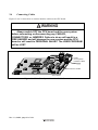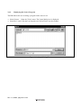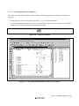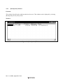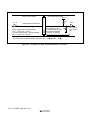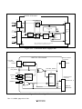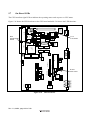
1
To all our customers Regarding the change of names mentioned in the document, such as Hitachi Electric and Hitachi XX, to Renesas Technology Corp. The semiconductor operations of Mitsubishi Electric and Hitachi were transferred to Renesas Technology Corporation on April 1st 2003. These operations include microcomputer, logic, analog and discrete devices, and memory chips other than DRAMs (flash memory, SRAMs etc.) Accordingly, although Hitachi, Hitachi, Ltd., Hitachi Semiconductors, and other Hitachi brand names are mentioned in the document, these names have in fact all been changed to Renesas Technology Corp. Thank you for your understanding. Except for our corporate trademark, logo and corporate statement, no changes whatsoever have been made to the contents of the document, and these changes do not constitute any alteration to the contents of the document itself. Renesas Technology Home Page: http://www.renesas.com Renesas Technology Corp. Customer Support Dept. April 1, 2003 Cautions Keep safety first in your circuit designs! 1. Renesas Technology Corporation puts the maximum effort into making semiconductor products better and more reliable, but there is always the possibility that trouble may occur with them. Trouble with semiconductors may lead to personal injury, fire or property damage. Remember to give due consideration to safety when making your circuit designs, with appropriate measures such as (i) placement of substitutive, auxiliary circuits, (ii) use of nonflammable material or (iii) prevention against any malfunction or mishap. Notes regarding these materials 1. These materials are intended as a reference to assist our customers in the selection of the Renesas Technology Corporation product best suited to the customer's application; they do not convey any license under any intellectual property rights, or any other rights, belonging to Renesas Technology Corporation or a third party. 2. Renesas Technology Corporation assumes no responsibility for any damage, or infringement of any third-party's rights, originating in the use of any product data, diagrams, charts, programs, algorithms, or circuit application examples contained in these materials. 3. All information contained in these materials, including product data, diagrams, charts, programs and algorithms represents information on products at the time of publication of these materials, and are subject to change by Renesas Technology Corporation without notice due to product improvements or other reasons. It is therefore recommended that customers contact Renesas Technology Corporation or an authorized Renesas Technology Corporation product distributor for the latest product information before purchasing a product listed herein. The information described here may contain technical inaccuracies or typographical errors. Renesas Technology Corporation assumes no responsibility for any damage, liability, or other loss rising from these inaccuracies or errors. Please also pay attention to information published by Renesas Technology Corporation by various means, including the Renesas Technology Corporation Semiconductor home page (http://www.renesas.com). 4. When using any or all of the information contained in these materials, including product data, diagrams, charts, programs, and algorithms, please be sure to evaluate all information as a total system before making a final decision on the applicability of the information and products. Renesas Technology Corporation assumes no responsibility for any damage, liability or other loss resulting from the information contained herein. 5. Renesas Technology Corporation semiconductors are not designed or manufactured for use in a device or system that is used under circumstances in which human life is potentially at stake. Please contact Renesas Technology Corporation or an authorized Renesas Technology Corporation product distributor when considering the use of a product contained herein for any specific purposes, such as apparatus or systems for transportation, vehicular, medical, aerospace, nuclear, or undersea repeater use. 6. The prior written approval of Renesas Technology Corporation is necessary to reprint or reproduce in whole or in part these materials. 7. If these products or technologies are subject to the Japanese export control restrictions, they must be exported under a license from the Japanese government and cannot be imported into a country other than the approved destination. Any diversion or reexport contrary to the export control laws and regulations of Japan and/or the country of destination is prohibited. 8. Please contact Renesas Technology Corporation for further details on these materials or the products contained therein. SH7751 CPU Board HS7751STC01H User’s Manual ADE-702-225 Rev. 1.0 09/22/00 Hitachi, Ltd. HS7751STC01HE(B) Cautions 1. Hitachi neither warrants nor grants licenses of any rights of Hitachi’s or any third party’s patent, copyright, trademark, or other intellectual property rights for information contained in this document. Hitachi bears no responsibility for problems that may arise with third party’s rights, including intellectual property rights, in connection with use of the information contained in this document. 2. Products and product specifications may be subject to change without notice. Confirm that you have received the latest product standards or specifications before final design, purchase or use. 3. Hitachi makes every attempt to ensure that its products are of high quality and reliability. However, contact Hitachi’s sales office before using the product in an application that demands especially high quality and reliability or where its failure or malfunction may directly threaten human life or cause risk of bodily injury, such as aerospace, aeronautics, nuclear power, combustion control, transportation, traffic, safety equipment or medical equipment for life support. 4. Design your application so that the product is used within the ranges guaranteed by Hitachi particularly for maximum rating, operating supply voltage range, heat radiation characteristics, installation conditions and other characteristics. Hitachi bears no responsibility for failure or damage when used beyond the guaranteed ranges. Even within the guaranteed ranges, consider normally foreseeable failure rates or failure modes in semiconductor devices and employ systemic measures such as fail-safes, so that the equipment incorporating Hitachi product does not cause bodily injury, fire or other consequential damage due to operation of the Hitachi product. 5. This product is not designed to be radiation resistant. 6. No one is permitted to reproduce or duplicate, in any form, the whole or part of this document without written approval from Hitachi. 7. Contact Hitachi’s sales office for any questions regarding this document or Hitachi semiconductor products. IMPORTANT INFORMATION READ FIRST • READ this user's manual before using this CPU board. • KEEP the user's manual handy for future reference. Do not attempt to use the CPU board until you fully understand its mechanism. CPU Board: Throughout this document, the term "CPU board" shall be defined as the following products produced only by Hitachi, Ltd. excluding all subsidiary products. • • • • CPU board Serial cable AC power cable AC power adapter The user system or a host computer is not included in this definition. Purpose of the CPU Board: This CPU board is a software and hardware development tool for systems employing the Hitachi microcomputer SH7751. Simple debugging functions such as debugging, performance evaluation, and development of the user system including the SH7751 are enabled by connecting the CPU board to a host computer. In addition, expansion boards can be installed in the slots; therefore, memory and I/O can be expanded. However, this CPU board must not be installed in user products to be used as part of the user products; it is limited to debugging and evaluation of user systems. This CPU board must only be used for the above purpose. Limited Applications: This CPU board is not authorized for use in MEDICAL, atomic energy, aeronautical or space technology applications without consent of the appropriate officer of a Hitachi sales company. Such use includes, but is not limited to, use in life support systems. Buyers of this CPU board must notify the relevant Hitachi sales offices before planning to use the product in such applications. Improvement Policy: Hitachi, Ltd. (including its subsidiaries, hereafter collectively referred to as Hitachi) pursues a policy of continuing improvement in design, performance, and safety of the CPU board. Hitachi reserves the right to change, wholly or partially, the specifications, design, user's manual, and other documentation at any time without notice. Target User of the CPU Board: This CPU board should only be used by those who have carefully read and thoroughly understood the information and restrictions contained in the user's manual. Do not attempt to use the CPU board until you fully understand its mechanism. It is highly recommended that first-time users be instructed by users that are well versed in the operation of the CPU board. Rev. 1.0, 09/00, page I of VI LIMITED WARRANTY Hitachi warrants its CPU board to be manufactured in accordance with published specifications and free from defects in material and/or workmanship. Hitachi, at its option, will repair or replace any CPU board returned intact to the factory, transportation charges prepaid, which Hitachi, upon inspection, determine to be defective in material and/or workmanship. The foregoing shall constitute the sole remedy for any breach of Hitachi's warranty. See the Hitachi warranty booklet for details on the warranty period. This warranty extends only to you, the original Purchaser. It is not transferable to anyone who subsequently purchases the CPU board from you. Hitachi is not liable for any claim made by a third party or made by you for a third party. DISCLAIMER HITACHI MAKES NO WARRANTIES, EITHER EXPRESS OR IMPLIED, ORAL OR WRITTEN, EXCEPT AS PROVIDED HEREIN, INCLUDING WITHOUT LIMITATION THEREOF, WARRANTIES AS TO MARKETABILITY, MERCHANTABILITY, FITNESS FOR ANY PARTICULAR PURPOSE OR USE, OR AGAINST INFRINGEMENT OF ANY PATENT. IN NO EVENT SHALL HITACHI BE LIABLE FOR ANY DIRECT, INCIDENTAL OR CONSEQUENTIAL DAMAGES OF ANY NATURE, OR LOSSES OR EXPENSES RESULTING FROM ANY DEFECTIVE CPU BOARD, THE USE OF ANY CPU BOARD, OR ITS DOCUMENTATION, EVEN IF ADVISED OF THE POSSIBILITY OF SUCH DAMAGES. EXCEPT AS EXPRESSLY STATED OTHERWISE IN THIS WARRANTY, THIS CPU BOARD IS SOLD "AS IS ", AND YOU MUST ASSUME ALL RISK FOR THE USE AND RESULTS OBTAINED FROM THE CPU BOARD. Rev. 1.0, 09/00, page II of VI State Law: Some states do not allow the exclusion or limitation of implied warranties or liability for incidental or consequential damages, so the above limitation or exclusion may not apply to you. This warranty gives you specific legal rights, and you may have other rights which may vary from state to state. The Warranty is Void in the Following Cases: Hitachi shall have no liability or legal responsibility for any problems caused by misuse, abuse, misapplication, neglect, improper handling, installation, repair or modifications of the CPU board without Hitachi's prior written consent or any problems caused by the user system. All Rights Reserved: This user's manual and CPU board are copyrighted and all rights are reserved by Hitachi. No part of this user's manual, all or part, may be reproduced or duplicated in any form, in hard-copy or machinereadable form, by any means available without Hitachi's prior written consent. Other Important Things to Keep in Mind: 1. Circuitry and other examples described herein are meant merely to indicate the characteristics and performance of Hitachi's semiconductor products. Hitachi assumes no responsibility for any intellectual property claims or other problems that may result from applications based on the examples described herein. 2. No license is granted by implication or otherwise under any patents or other rights of any third party or Hitachi. Figures: Some figures in this user's manual may show items different from your actual system. Limited Anticipation of Danger: Hitachi cannot anticipate every possible circumstance that might involve a potential hazard. The warnings in this user's manual and on the CPU board are therefore not all inclusive. Therefore, you must use the CPU board safely at your own risk. Rev. 1.0, 09/00, page III of VI SAFETY PAGE READ FIRST • READ this user's manual before using this CPU board. • KEEP the user's manual handy for future reference. Do not attempt to use the CPU board until you fully understand its mechanism. DEFINITION OF SIGNAL WORDS This is the safety alert symbol. It is used to alert you to potential personal injury hazards. Obey all safety messages that follow this symbol to avoid possible injury or death. DANGER WARNING CAUTION CAUTION DANGER indicates an imminently hazardous situation which, if not avoided, will result in death or serious injury. WARNING indicates a potentially hazardous situation which, if not avoided, could result in death or serious injury. CAUTION indicates a potentially hazardous situation which, if not avoided, may result in minor or moderate injury. CAUTION used without the safety alert symbol indicates a potentially hazardous situation which, if not avoided, may result in property damage. NOTE emphasizes essential information. Rev. 1.0, 09/00, page IV of VI WARNING Observe the precautions listed below. Failure to do so will result in a FIRE HAZARD and will damage the user system and the CPU board or will result in PERSONAL INJURY. The USER PROGRAM will be LOST. 1. Always satisfy the power supply conditions which are described in the manual. Ensure that there are no short circuits between VCC and GND. Do not apply voltage that is outside the guaranteed range. 2. Always switch OFF the CPU board and the user system before connecting or disconnecting any CABLES, connectors, or jumpers. 3. When turning on the CPU board or the user system, take care that conductive material does not touch the CPU board or the user system. 4. Check that the pin numbers on the connectors of the CPU board and those on the user system are correctly aligned before connecting the CPU board and the user system. Rev. 1.0, 09/00, page V of VI Rev. 1.0, 09/00, page VI of VI Preface Thank you for purchasing the CPU board for Hitachi’s SH7751 microcomputer. The CPU board is an efficient development tool for software and hardware of systems based on Hitachi’s SH7751 microcomputer. This manual explains the functions and method of operation of the CPU board. Section 1, Overview, describes the hardware system configuration and explains environment settings to enable board use. Section 2, Preparations Before Use, explains procedures for using the CPU board, HDI installation, various connections, and the power supply specifications. Section 3, Tutorial, introduces the major HDI features while demonstrating methods for loading and debugging a C language program. Section 4, Descriptions of Windows, describes each of the windows used in the HDI. Section 5, CPU Board Specifications, explains the specifications of the CPU board, the memory map, interfaces with external equipment, and CPU board initialization. Section 6, Notes and Troubleshooting, explains important information regarding use and gives suggestions for troubleshooting. Section 7, Creation of User Interrupt Handlers, explains how to create an original interrupt handler routine. Please read this manual completely in order to gain a thorough understanding of this product’s functions and performance. The text appearing in the various windows of the HDI may differ from those appearing in this manual depending on the language of the OS being used. The figures appearing in this manual are for the ® ® Microsoft Windows 98. Related Manuals • SH7751 Hardware Manual • SH4 Programming Manual • SH Series Cross Assembler User’s Manual • SH Series C Compiler User’s Manual • SH Series Simulator/Debugger User’s Manual • Hitachi Debugging Interface User's Manual (available in the CD-R supplied with this CPU board) When connecting an E10A emulator to the CPU board, the following manual should also be read. Rev. 1.0, 09/00, page i of x • SH7751 E10A Emulator User’s Manual Notes: 1. IBM PC is a registered trademark of International Business Machines Corporation in the United States. 2. Microsoft, Windows, and WindowsNT are registered trademarks of Microsoft Corporation in the United States and/or other countries. Rev. 1.0, 09/00, page ii of x Contents Section 1 Overview........................................................................................... 1 1.1 1.2 1.3 1.4 1.5 1.6 Features............................................................................................................................. 1 System Configuration ....................................................................................................... 2 Warnings........................................................................................................................... 3 Components ...................................................................................................................... 4 CD-R Contents.................................................................................................................. 5 Environmental Conditions ................................................................................................ 6 Section 2 Preparation before Use ....................................................................... 7 2.1 2.2 2.3 2.4 2.5 2.6 2.7 2.8 2.9 CPU Board Preparation .................................................................................................... 7 HDI Installation ................................................................................................................ 8 HDI Uninstallation............................................................................................................ 9 Connecting Cables ............................................................................................................ 10 Connecting the User Expansion Board ............................................................................. 12 Connecting the Compact PCI Backplane.......................................................................... 13 Switches............................................................................................................................ 16 Jumpers ............................................................................................................................. 17 Power Supply.................................................................................................................... 20 2.9.1 Power-Supply Specifications............................................................................... 20 2.9.2 Connecting the Power Supply Cable ................................................................... 21 Section 3 Tutorial ............................................................................................... 23 3.1 3.2 3.3 3.4 3.5 3.6 3.7 3.8 3.9 3.10 3.11 3.12 3.13 Introduction ...................................................................................................................... 23 Running the HDI............................................................................................................... 24 [HDI] Window.................................................................................................................. 26 Setting up the CPU Board................................................................................................. 27 Setting the [Monitor Setup] Dialog Box ........................................................................... 27 Downloading the Tutorial Program .................................................................................. 29 3.6.1 Downloading the Tutorial Program ..................................................................... 29 3.6.2 Displaying the Source Program ........................................................................... 30 Setting the Software Breakpoint ....................................................................................... 32 Setting Registers ............................................................................................................... 33 Executing the Program ..................................................................................................... 35 Reviewing Breakpoints..................................................................................................... 38 Viewing Memory.............................................................................................................. 39 Watching Variables........................................................................................................... 40 Stepping Through a Program............................................................................................ 43 3.13.1 Executing [Step In] Command ............................................................................ 44 3.13.2 Executing [Step Out] Command.......................................................................... 45 Rev. 1.0, 09/00, page iii of x 3.14 3.15 3.16 3.17 3.18 3.13.3 Executing [Step Over] Command........................................................................ 47 Displaying Local Variables .............................................................................................. 49 Software Break Function .................................................................................................. 50 Run Time Count Function ................................................................................................ 53 Saving a Session ............................................................................................................... 58 What Next? ....................................................................................................................... 59 Section 4 Descriptions of Windows....................................................................61 4.1 4.2 HDI Windows................................................................................................................... 61 Descriptions of Each Window .......................................................................................... 64 4.2.1 [Monitor Setup] Dialog Box................................................................................ 64 4.2.3 [Add/Edit Breakpoint] Dialog Box...................................................................... 68 4.2.4 [System Status] Window ..................................................................................... 69 4.2.5 [Run Time Count Condition] Dialog Box ........................................................... 71 4.2.6 [Cache Control] Dialog Box................................................................................ 72 4.2.7 [Simulated I/O Window] Window....................................................................... 73 4.2.8 [Command Line] Window................................................................................... 74 Section 5 CPU Board Specifications .................................................................75 5.1 5.2 5.3 5.4 5.5 5.6 5.7 5.8 5.9 Block Diagram.................................................................................................................. 75 Specifications.................................................................................................................... 76 Memory Map .................................................................................................................... 78 External Interface ............................................................................................................. 80 5.4.1 Serial Interface..................................................................................................... 80 5.4.2 EPROM Socket Interface .................................................................................... 82 5.4.3 LAN Interface...................................................................................................... 83 5.4.4 User Expansion Board Interface.......................................................................... 86 5.4.5 PCI Interface........................................................................................................ 96 On-Board Registers .......................................................................................................... 101 E10A Emulator Interface.................................................................................................. 106 On-Board LEDs ................................................................................................................ 108 Parts Layout...................................................................................................................... 110 Initialization...................................................................................................................... 114 5.9.1 Initializing Resources .......................................................................................... 114 5.9.2 Procedure for Making Initial Settings of the CPU Bus State Controller (BSC) .. 116 5.9.3 Initial Settings of CPU Bus State Controller (BSC) ............................................ 117 Section 6 Notes and Troubleshooting................................................................123 6.1 6.2 Notes................................................................................................................................. 123 Troubleshooting................................................................................................................ 129 Section 7 Creation of User Interrupt Handlers ..................................................131 7.1 7.2 Creation of User Interrupt Handlers ................................................................................. 131 User Program Using SCIF ................................................................................................ 133 7.2.1 Creation of SCIF Driver ...................................................................................... 133 Rev. 1.0, 09/00, page iv of x 7.3 7.2.2 SCIF-Related Register Settings ........................................................................... 133 Sample Program................................................................................................................ 136 Rev. 1.0, 09/00, page v of x Figure Figure 1.1 CPU Board, External View ...................................................................................... 1 Figure 1.2 CPU Board System Configuration ........................................................................... 2 Figure 2.1 CPU Board Preparation Flow Chart......................................................................... 7 Figure 2.2 [Setup.exe] Icon ....................................................................................................... 8 Figure 2.3 Start Menu................................................................................................................ 9 Figure 2.4 E10A User System Interface Cable Connection ...................................................... 10 Figure 2.5 Serial Interface Cable Connection ........................................................................... 11 Figure 2.6 AC Adapter Connection........................................................................................... 11 Figure 2.7 User Expansion Board Connection (CN1) ............................................................... 12 Figure 2.8 Compact PCI Backplane Connection....................................................................... 13 Figure 2.9 Spacer Removal ....................................................................................................... 14 Figure 2.10 Front Panel Attachment ......................................................................................... 15 Figure 2.11 Switch Location ..................................................................................................... 16 Figure 2.12 Jumper Insertion..................................................................................................... 19 Figure 2.13 Power-Supply Specifications ................................................................................. 20 Figure 2.14 Power-Supply Section Block Diagram .................................................................. 20 Figure 2.15 Front View of Power Supply Connector ............................................................... 21 Figure 2.16 AC Power Supply Adapter Connection ................................................................ 22 Figure 3.1 [Start] Menu ............................................................................................................. 24 Figure 3.2 [Select Session] Dialog Box..................................................................................... 24 Figure 3.3 Power Supply Confirmation Message Box .............................................................. 25 Figure 3.4 [HDI] Window ......................................................................................................... 26 Figure 3.5 [Monitor Setup] Dialog Box .................................................................................... 27 Figure 3.6 [Load Program] Dialog Box .................................................................................... 29 Figure 3.7 [HDI] Message Box ................................................................................................. 29 Figure 3.8 [Open] Dialog Box................................................................................................... 30 Figure 3.9 [Program] Window (Displaying the Source Program)............................................. 31 Figure 3.10 [Program] Window (Setting a Software Breakpoint)............................................. 32 Figure 3.11 [Registers] Window ............................................................................................... 33 Figure 3.12 [Register] Dialog Box (PC).................................................................................... 34 Figure 3.13 [Register] Dialog Box (SP) .................................................................................... 34 Figure 3.14 [Go] Button ............................................................................................................ 35 Figure 3.15 [Program] Window (Break Status)......................................................................... 35 Figure 3.16 [System Status] Window........................................................................................ 36 Figure 3.17 [Breakpoints] Window........................................................................................... 38 Figure 3.18 [Open Memory Window] Dialog Box ................................................................... 39 Figure 3.19 [Word Memory] Window ...................................................................................... 39 Figure 3.20 [Instant Watch] Dialog Box ................................................................................... 40 Figure 3.21 [Watch Window] Window (Displaying the Array)................................................ 41 Figure 3.22 [Add Watch] Dialog Box ....................................................................................... 41 Figure 3.23 [Watch Window] Window (Displaying the Variable) ............................................ 42 Figure 3.24 [Watch Window] Window (Displaying Array Elements) ...................................... 42 Rev. 1.0, 09/00, page vi of x Figure 3.25 [Program] Window (Step Execution)..................................................................... 43 Figure 3.26 [Step In] Button...................................................................................................... 44 Figure 3.27 [Program] Window (Step In) ................................................................................. 44 Figure 3.28 [Step Out] Button ................................................................................................... 45 Figure 3.29 [Program] Window (Step Out)............................................................................... 45 Figure 3.30 [Program] Window (Step In −> Step In)................................................................ 46 Figure 3.31 [Step Over] Button ................................................................................................. 47 Figure 3.32 [Program] Window (Before Step Over Execution)................................................ 47 Figure 3.33 [Program] Window (Step Over)............................................................................. 48 Figure 3.34 [Locals] Window.................................................................................................... 49 Figure 3.35 [Breakpoints] Window (Before setting software break) ......................................... 50 Figure 3.36 [Add/Edit Breakpoint] Dialog Box ......................................................................... 51 Figure 3.37 [Breakpoints] Window (Software Breakpoint Setting) .......................................... 51 Figure 3.38 [Program] Window at Execution Stop (Software Break)........................................ 52 Figure 3.39 Displayed Contents of the [System Status] Window (Software Break) .................. 52 Figure 3.40 [Program] Window (Break before Run Time Count) ............................................ 53 Figure 3.41 [System Status] Window (Run Time Count Disabled) .......................................... 54 Figure 3.42 [Run Time Count Condition] Dialog Box.............................................................. 54 Figure 3.43 [Program] Window (Stopped at a Breakpoint after Run Time Count) .................. 56 Figure 3.44 [System Status] Window (Run Time Count Result) .............................................. 57 Figure 4.1 [Monitor Setup] Dialog Box .................................................................................... 64 Figure 4.2 [Breakpoints] Window ............................................................................................. 66 Figure 4.3 [Add/Edit Breakpoint] Dialog Box .......................................................................... 68 Figure 4.4 [System Status] Window.......................................................................................... 69 Figure 4.5 [Run Time Count Condition] Window..................................................................... 71 Figure 4.6 [Cache Control] Dialog Box .................................................................................... 72 Figure 4.7 [Simulated I/O Window] Window ........................................................................... 74 Figure 5.1 Block Diagram of the CPU board ............................................................................ 75 Figure 5.2 CPU Board Memory Map ........................................................................................ 79 Figure 5.3 Connection to Host Computer.................................................................................. 81 Figure 5.4 Serial Interface Connector Pin Arrangement ........................................................... 82 Figure 5.5 User Expansion Board Interface Connector CN1 Pin Arrangement ........................ 87 Figure 5.6 Bus Release Timing (1)............................................................................................ 90 Figure 5.7 Bus Release Timing (2)............................................................................................ 91 Figure 5.8 Example of CKIO Terminal Resistor Connection.................................................... 92 Figure 5.9 Configuration of User Expansion Board Interface Circuit (CN1)-1 ........................ 93 Figure 5.10 Configuration of User Expansion Board Interface Circuit (CN1)-2 ...................... 94 Figure 5.11 Configuration of User Expansion Board Interface Circuit (CN1)-3 ...................... 95 Figure 5.12 Compact PCI interface CN19 and CN20 Pin Arrangements.................................. 96 Figure 5.13 CPU Board Power Supply Lines........................................................................... 100 Figure 5.14 Reset Signal Lines................................................................................................. 100 Figure 5.15 Hitachi-UDI Port Connector (CN23) Pin Arrangement........................................ 106 Figure 5.16 LED Locations ...................................................................................................... 108 Figure 5.17 Parts Layout (Mounting Side) ................................................................................. 113 Figure 5.18 Procedure for Setting BSC Settings ...................................................................... 116 Rev. 1.0, 09/00, page vii of x Figure 6.1 Error Message Displayed at Exception (Instruction TLB Miss Exception)............ 124 Figure 6.2 Dialog Box Indicating Breakpoint Cannot Be Set .................................................. 124 Figure 6.3 Power-on Reset Input Message Box ....................................................................... 125 Figure 6.4 Manual Reset Input Message Box........................................................................... 125 Figure 7.1 Executing the Sample Program................................................................................ 136 Rev. 1.0, 09/00, page viii of x Table Table 1.1 Table 1.2 Table 1.3 Table 1.4 Table 2.1 Table 2.2 Table 2.3 Table 3.1 Table 3.2 Table 3.3 Table 3.4 Table 3.5 Table 3.6 Table 3.7 Table 4.1 Table 4.2 Table 4.3 Table 4.4 Table 4.5 Table 4.6 Table 4.7 Table 4.8 Table 4.9 Table 5.1 Table 5.2 Table 5.3 Table 5.4 Table 5.5 Table 5.6 Table 5.7 Table 5.8 Table 5.9 Table 5.10 Table 5.11 Table 5.12 Table 5.13 Table 5.14 Table 5.15 Table 5.16 Table 5.17 Table 5.18 Table 6.1 CPU Board Component List .................................................................................. 4 CD-R Contents ....................................................................................................... 5 Environmental Conditions ..................................................................................... 6 Operating Environments ........................................................................................ 6 Default Installation Directory ................................................................................ 8 Switch Specifications ............................................................................................. 16 Jumper Settings ...................................................................................................... 18 Tutorial Program Configuration............................................................................. 23 Check Items When HDI Cannot Be Initiated ......................................................... 25 Setting the [Monitor Setup] Dialog Box ................................................................ 28 Contents of the [System Status] Window............................................................... 37 Step Option ............................................................................................................ 43 Items Set in [Run Time Count Condition] Dialog Box.......................................... 55 Selectable Measurement Units ............................................................................... 55 HDI Window Menus and Related Manual Entries................................................. 61 [Monitor Setup] Dialog Box Page.......................................................................... 65 [Breakpoints] Window Display Items.................................................................... 67 [Breakpoints] Window Pop-up Menu Operation ................................................... 67 [Add/Edit Breakpoint] Dialog Box Items .............................................................. 68 [System Status] Window Display Items................................................................. 70 [Run Time Count Condition] Dialog Box Items ................................................... 71 Selectable Measurement Units ............................................................................... 72 [Cache Control] Dialog Box Items......................................................................... 73 External Specifications.......................................................................................... 76 Pin Assignment of the Serial Interface Connector ................................................. 80 Serial Interface Specifications................................................................................ 81 Pin Assignment of the EPROM Socket.................................................................. 83 LAN91C96 LAN Controller Register Specifications (Bank 0).............................. 84 LAN91C96 LAN Controller Register Specifications (Bank 1).............................. 84 LAN91C96 LAN Controller Register Specifications (Bank 2).............................. 85 LAN91C96 LAN Controller Register Specifications (Bank 3).............................. 85 LAN91C96 LAN Controller Register Specifications (Bank 4).............................. 86 Pin Assignment of User Expansion Board Interface Connector CN1.................... 88 AC Specifications................................................................................................... 91 Compact PCI Interface J1 Connector (CN19) Pin Assignments............................ 97 Compact PCI Interface J2 Connector (CN20) Pin Assignments............................ 98 On-Board Registers................................................................................................ 101 Hitachi-UDI Port Connector (CN23) Pin Assignment........................................... 107 LED Functions ....................................................................................................... 109 List of Uninstalled Parts......................................................................................... 110 Resource Initialization ........................................................................................... 114 Watchdog Timer Register ...................................................................................... 127 Rev. 1.0, 09/00, page ix of x Table 6.2 Table 7.1 Table 7.2 Table 7.3 Table 7.4 Table 7.5 Register Initial Value Settings ............................................................................... 129 Interrupt Causes and Branch Addresses for User Interrupt Handlers .................... 131 HALT Break Destination Address ......................................................................... 133 Sample Program Files ............................................................................................ 137 Sections for the Sample Program........................................................................... 137 Interrupt Processing in the Sample Program.......................................................... 138 Rev. 1.0, 09/00, page x of x Section 1 Overview 1.1 Features The SH7751 CPU board (hereafter, referred to as the CPU board) supports the evaluation of the functions and performance of the Hitachi SH7751 microcomputer, and the development and evaluation of systems that incorporate the SH7751. The features of this CPU board are as follows: • Supports user expansion boards Has an expansion connector for I/O of signals conforming to the SH7751 external bus specifications, to which an expansion board developed by the user to increase memory and I/O can be connected and evaluated. • Supports the maximum operating frequency Allows evaluation at 167 MHz and 83.5 MHz, which are the maximum internal and external operating frequencies of the SH7751, respectively. • Host Interface For interfacing with IBM PC compatible as the host computer, one channel of serial interface (that conforms to RS-232C) is provided. The Hitachi Debugging Interface (HDI) is also provided as host interface software. • Enables user-program evaluation Up to 63.5 Mbytes of a user program can be loaded into the user memory and be evaluated. • Support for compact PCI interface The SH7751 provides PCI interface functions. The CPU board outputs the on-chip PCI bus interface signals through the compact PCI connector. This interface conforms to the PICMG2.0 rev.2.1, and the CPU board functions can be easily expanded by connecting to a standard backplane. Figure 1.1 CPU Board, External View Rev. 1.0, 09/00, page 1 of 138 1.2 System Configuration The system configuration of the CPU board is shown in figure 1.2. The following items are required to use the CPU board. • IBM PC compatible machine: One for the monitor command input and output. Use the provided cable. • One serial interface cable: • One AC power supply adapter: Use the provided adapter. Use the provided power cable. • One AC power supply cable: AC power supply adapter CPU board Serial interface cable IBM PC compatible Figure 1.2 CPU Board System Configuration Rev. 1.0, 09/00, page 2 of 138 1.3 Warnings CAUTION READ the following warnings before using the CPU board. Incorrect operation will damage the user system and the CPU board. The USER PROGRAM will be LOST. 1. Check all components against the component list after unpacking the CPU board. 2. Never place heavy objects on the CPU board. 3. Protect the CPU board from excessive impacts and stresses. For details, refer to section 1.6, Environmental Conditions. 4. Do not connect any cable or connector other than specified ones to the CPU board. 5. When moving the host computer or user expansion board, take care not to vibrate or damage the CPU board. 6. After connecting the cable, check that it is connected correctly. For details, refer to section 2, Preparation before Use. 7. Supply power to the connected equipment after connecting all cables. Cables must not be connected or removed while the power is on. Rev. 1.0, 09/00, page 3 of 138 1.4 Components Table 1.1 lists the components of the CPU board. Check all components after unpacking. Table 1.1 CPU Board Component List Item View Quantity Remarks CPU board 1 AC power supply adapter 1 AC power supply cable 1 Serial interface cable 1 Jumper 4 Front panel 1 For use in a compact PCI rack. provided with handles CD-R (HDI installer) 1 One CD-R; SH7751 CPU Board Installation Guide 2 MRST PRST ABORT Rev. 1.0, 09/00, page 4 of 138 Debug Serial Port LAN I/F One printed circuit board Model number HS7751STC01SR (contains CPU board manual and HDI manual) xxxxxxx xxxxxxx One Japanese version and one English version; Japanese: HS7751STC01HJ-P, English: HS7751STC01HE-P 1.5 CD-R Contents The supplied CD-R includes software and user's manuals for the SH7751 CPU board as listed in table 1.2. Table 1.2 CD-R Contents Directory File Name Contents Remarks \Setup Setup.exe HDI installer \Manuals\Japanese HS7751STC01HJ.pdf SH7751 CPU Board User's Manual PDF document in Japanese Type No.: HS7751STC01HJ \Manuals\Japanese HS6400DIIW5SJ.pdf Hitachi Debugging Interface User's Manual PDF document in Japanese Type No.: HS6400DIIW5SJ \Manuals\English HS7751STC01HE.pdf SH7751 CPU Board User's Manual PDF document in English Type No.: HS7751STC01HE \Manuals\English HS6400DIIW5SE.pdf Hitachi Debugging Interface User's Manual PDF document in English Type No.: HS6400DIIW5SE \Pdf_read\Japanese Ar40jpn.exe Acrobat Reader installer \Pdf_read\Englsih Ar40eng.exe Acrobat Reader installer @ Japanese version @ English version @ Note: To read a PDF document, use the Acrobat Reader. Rev. 1.0, 09/00, page 5 of 138 1.6 Environmental Conditions CAUTION Observe the conditions listed in tables 1.3 and 1.4 when using the CPU board. Failure to do so will damage the user expansion board and the CPU board. The USER PROGRAM will be LOST. Table 1.3 Environmental Conditions Item Specifications Temperature Operating: +10°C to +35°C Storage: –10°C to +50°C Humidity Operating: 35% RH to 80% RH, no condensation Storage: 35% RH to 80% RH, no condensation Vibration Operating: 2.45 m/s max. 2 Storage: 4.9 m/s max. 2 Transportation: 14.7 m/s max. Ambient gases There must be no corrosive gases present Table 1.4 2 Operating Environments Item Description Host computer Built-in Pentium or higher-performance CPU (200 MHz or higher recommended); IBM PC or compatible machine. OS Windows 95, Windows 98, or Windows NT Minimum memory capacity 32 Mbytes or more (double of the load module size recommended) Hard-disk capacity Installation disk capacity: 5 Mbytes or more. (Prepare an area at least double the memory capacity (four-times or more recommended) as the swap area.) CD-ROM drive Required to install the HDI. Pointing device such as mouse Connectable to the host computer; compatible with Windows 95, ® ® Windows 98, and Windows NT . Power voltage Input: 100 to 240 VAC, 50/60 Hz, 0.6 A max. (AC power supply adapter) Output: +5 VDC 5 A ® ® ® ® Rev. 1.0, 09/00, page 6 of 138 Section 2 Preparation before Use 2.1 CPU Board Preparation WARNING READ the reference sections shaded in figure 2.1 before using the CPU board product. Incorrect operation will damage the CPU board and the user expansion board. The USER PROGRAM will be LOST. Unpack the CPU board and prepare it for use as follows: Reference Unpack the CPU board. Check the components against the component list. Component list Turn on the host computer. Section 2.2 Install the HDI. Procedure when the CPU board is used first. Turn off the host computer. Connect the CPU board to the host computer and AC power supply adapter, and when necessary to a Compact PCI back plane or user expansion board. Also be sure to set the jumper on the CPU board. Section 2.3 to 2.8 Procedure when the CPU board is used for second time or later. Turn on the host computer. Turn on the CPU board. Section 3 Start the HDI. Figure 2.1 CPU Board Preparation Flow Chart Rev. 1.0, 09/00, page 7 of 138 2.2 HDI Installation An example of installing the HDI on an IBM PC compatible machine is described in this section. Start [Setup.exe] in the \Setup directory of the HDI installer CD-R. If any other application is running, close it before starting the HDI installer. Figure 2.2 [Setup.exe] Icon This runs the HDI installer. A dialog box will first prompt you to select a language for the installation process. Select a language then continue according to the instructions displayed by the installer. @ Note: Under Windows NT 4.0, install the HDI in the administrator mode. HDI Installation Directory: The default directory for installing the HDI depends on whether the Hitachi Embedded Workshop (HEW) has been installed in the host computer, as shown in table 2.1 Table 2.1 Default Installation Directory HEW Program Default Installation Directory HEW has not been installed C:\Hdi5_cb\7751 HEW has been installed (in this example, in C:\HEW) C:\Hew\Hdi5\Cb\7751 Backup File: If another version of HDI has already been installed, a message "The HDI.INI file has already existed. Can it be overwritten?" will be displayed. Clicking [Yes] will make a backup of the existing file in the Backup directory of the installation directory. When installation is complete, [HDI for SH7751 CPU board] can be selected from the start menu. Rev. 1.0, 09/00, page 8 of 138 Figure 2.3 Start Menu 2.3 HDI Uninstallation Uninstall the HDI for the SH7751 CPU board as follows: 1. Select [Settings] from the Start menu, then select [Control Panel]. 2. Select [Add/Remove Programs]. 3. Select [HDI for SH7751 CPU board] from the application list, then click [Add/Remove]. 4. A confirmation message will be displayed, and the uninstallation procedure will start. Rev. 1.0, 09/00, page 9 of 138 2.4 Connecting Cables Figures 2.4 to 2.6 show how to connect interface cables to the CPU board. WARNING Always switch OFF the CPU board and the user system before connecting or disconnecting any CABLES, CONNECTORS, or JUMPERS. Failure to do so will result in a FIRE HAZARD and will damage the user system and the CPU board or will result in PERSONAL INJURY. The USER PROGRAM will be LOST. E10A user system interface cable Connect to CN23 CPU board Figure 2.4 E10A User System Interface Cable Connection Rev. 1.0, 09/00, page 10 of 138 Connect to CN15 Serial interface cable Figure 2.5 Serial Interface Cable Connection WARNING Always switch OFF the CPU board and the user system before connecting or disconnecting any CABLES. Failure to do so will result in a FIRE HAZARD and will damage the user expansion board and the CPU board or will result in PERSONAL INJURY. The USER PROGRAM will be LOST. Connect to CN3 from AC adapter CPU board Figure 2.6 AC Adapter Connection Rev. 1.0, 09/00, page 11 of 138 2.5 Connecting the User Expansion Board Figure 2.7 shows how to connect the user expansion board. WARNING Always switch OFF the CPU board and the user system before connecting or disconnecting any CABLES, CONNECTORS, or JUMPERS. Failure to do so will result in a FIRE HAZARD and will damage the user system and the CPU board or will result in PERSONAL INJURY. The USER PROGRAM will be LOST. Connect to CN1 User expansion board CPU board Figure 2.7 User Expansion Board Connection (CN1) Rev. 1.0, 09/00, page 12 of 138 2.6 Connecting the Compact PCI Backplane Figure 2.8 shows how to connect the compact PCI backplane. WARNING Always switch OFF the CPU board and the user system before connecting or disconnecting any CABLES, CONNECTORS, or JUMPERS. Failure to do so will result in a FIRE HAZARD and will damage the user system and the CPU board or will result in PERSONAL INJURY. The USER PROGRAM will be LOST. Compact PCI backplane (commercially available) System slot CPU board Expansion slots Commercially available PCI board Figure 2.8 Compact PCI Backplane Connection The CPU board can be used as a system board for compact PCI. Install the CPU board in the system board slot of the backplane. The 3.3V, 33MHz, and 32bit interface is supported. Up to four expansion slots can be controlled. Before installing the CPU board in the backplane, remove the spacers and attach the front panel as shown in figures 2.9 and 2.10. Do not lose the spacers and screws removed. Rev. 1.0, 09/00, page 13 of 138 CN2 76 1084 LT U8 U16 100 75 U40 51 25 FPGA EPM7128 1 50 26 1 64 M2 U37 M7 CDC2509 U43 CN16 16245 U20 CN15 65 256 U42 SML210 D13-16 OSC6 76 L13 L15 75 14 U33 26 50 L16 L14 51 25 14 U47 U49 U51 16245 U24 08 U32 FPGA EPM7128 1 SG8002CA 3.6864MHz 100 HC164 U34 SML210 244 U41 D18-21 HC138 J2 jumper J3 jumper U52 U23 16245 QS3384 U44 J1 jumper U19 16245 QS3384 U45 J4 jumper U22 16245 SW4 SW3 SW2 SG8002CA 33MHz CN4 MRST U48 OSC4 C226 FCT3805 Figure 2.9 Spacer Removal AROBT C57 PRST C227 Transformer S5569003-10 50 U21 CN18 M6 M5 M4 M3 U1 M1 LT1330 SG8002CA 27.83MHz OSC3 MB 3771 TDA 1308 51 26 U26 25 128 X2 SH7751 QFP CN20 193 MC306 32.768KHz 192 D22 C28 129 C27 CN23 76 Ether 91C94 U7 U27 C20 SML210 D1 D2 D375 100 1 SG8002 20MHz U25 U28 U11 C29 U10 uBGA G28F640 uBGA G28F640 uBGA G28F640 uBGA G28F640 OSC1 U9 16245 16245 C21 C89 C101 PUG16 -30 C26 L7 16245 16245 16245 LT 1084 C3 Spacer locations J21 Rev. 1.0, 09/00, page 14 of 138 F1 D12 CN19 C182 AT93C46 C82 C4 V03 C2 RUE-500 C181 CN1(53481-1809) CN3 C171 HM5225165 HM5225165 Spacer locations SW1 C170 CPU board Screws to the two spacer holes. Front panel Figure 2.10 Front Panel Attachment Rev. 1.0, 09/00, page 15 of 138 2.7 Switches Table 2.2 lists the switches used in the CPU board and figure 2.11 shows where the switches are located (on the CPU board). Table 2.2 Switch Specifications Switch Symbol Type Function Power supply switch SW1 Rocker switch Turns on and off the 5 V power supplied to the CPU board. Turn off this switch when connecting to the compact PCI backplane. Manual reset switch SW2 Push button (red) Forcibly initializes the system. Use this switch when the system does not operate correctly, for example, when the user program goes out of control. The BSC settings are not initialized. Power-on reset switch SW3 Push button (white) Forcibly initializes the system. Use this switch when the system does not operate correctly, for example, when the user program goes out of control. The BSC settings are reset to the HDI initial settings. Abort switch SW4 Push button (black) Forcibly aborts the command currently being executed. When this button is pressed while the user program is being executed, the CPU board stops execution and returns to the monitor program command wait state. Power supply switch CPU board Power-on reset switch Abort switch Manual reset switch Figure 2.11 Switch Location Rev. 1.0, 09/00, page 16 of 138 2.8 Jumpers The CPU board has 33 locations for jumpers: J11 to J16, J21 to J2A, J31 to J36 and J41 to J4B. • J11 to J16: For test in Hitachi. No jumpers are mounted. • J21 to J21A: For specifying the CPU board operating mode. J21, J23 and J25 to J27 are mounted. • J31 to J36: • J41 to J4B: For specifying expansion functions. J35 and J36 are mounted. For specifying the SH7751 modes. J42, J46, J49, J4A, and J4B are mounted. Table 2.3 shows jumper settings. In the table, the initial settings at shipment are shaded. The reserved settings must not be used. Figure 2.12 shows how to insert a jumper pin. WARNING Always switch OFF the CPU board and the user system before connecting or disconnecting any CABLES, CONNECTORS, or JUMPERS. Failure to do so will result in a FIRE HAZARD and will damage the user system and the CPU board or will result in PERSONAL INJURY. The USER PROGRAM will be LOST. Rev. 1.0, 09/00, page 17 of 138 Table 2.3 Jumper Settings Symbol Function Setting Description J21 Base clock 1-2 closed Reserved (must not be used) 2-3 closed On-board clock (27.8 MHz) Closed CPU internal frequency 167 MHz Bus frequency 55.7 MHz J23 Bus frequency CPU on-chip module frequency 27.8 MHz Open CPU internal frequency 167 MHz Bus frequency 83.5 MHz CPU on-chip module frequency 41.8 MHz J25 J26 Resource for area 0 Closed Expansion bus area 2 EPROM (socket) connected. Flash memory is connected to area 2. Open Flash memory (containing HDI) connected. Closed Area 2 released to the user expansion board interface Open Area 2 cannot be used J27 Expansion bus area 4 Closed Area 4 released to the user expansion board interface Open Area 4 cannot be used J35 PCI clock 1-2 closed On-board clock (33 MHz) 2-3 closed Reserved (must not be used) J36 Serial interface baud rate Closed 57,600 bit/s Open 115,200 bit/s CPU clock mode Closed Clock mode 5 Open Reserved (must not be used) J42 J46 CPU endian Closed Big endian Open Little endian J49 CPU clock source Closed Pulse input to EXTAL of CPU Open Reserved (must not be used) J4A CPU PCI clock Closed Input to PCICLK pin Open Reserved (must not be used) J4B CPU PCI function Closed PCI function enabled Open PCI function disabled Note: When the EPROM is selected by J25, area 2 becomes the flash memory area regardless of the J26 setting, and the expansion bus area cannot be accessed in area 2. The CS0 bus width is switched between 32 bits (flash memory is connected) and 16 bits (EPROM is connected) by the J25 setting. Rev. 1.0, 09/00, page 18 of 138 CPU board Jumper Figure 2.12 Jumper Insertion Rev. 1.0, 09/00, page 19 of 138 2.9 Power Supply 2.9.1 Power-Supply Specifications Figure 2.13 shows the power-supply specifications, and figure 2.14 shows the block diagram of the power-supply section. 5 V (Vin) 5.0V 3.3 V (Vout) 1.8 V (CPU) 3.3 V 2.6 V 2.6 V 1.8 V 20 ms (reference value) 50 ms Power-on reset_N Figure 2.13 Power-Supply Specifications SH7751 CPU board CN3 +5 V SW1 Power connector GND ON CN1 SW1-1 +5 V GND OFF +5 V CN19 CN20 PCI connector LT1084 Out 5 V -> 3.3 V Regulator ON SW1-2 SH7751 CPU In +3.3 V LT1084 3.3 V -> 1.8 V Out Regulator OFF GND GND 3.3 V +5 V In +3.3 V 5V On-board logic Expansion bus connector +3.3 V VCCIO VCC GND 1.8 V GND SW1-1 and SW1-2 are included in one component. They are switched on or off at the same time. Figure 2.14 Power-Supply Section Block Diagram Rev. 1.0, 09/00, page 20 of 138 2.9.2 Connecting the Power Supply Cable Power should always be supplied to the CPU board using the provided AC power supply adapter and AC power supply cable. The method of connection is shown in figures 2.15 and 2.16. WARNING Observe the precautions listed below. Failure to do so will result in a FIRE HAZARD and will damage the user system and the CPU board or will result in PERSONAL INJURY. The USER PROGRAM will be LOST. 1. Always use the provided AC power supply adapter. 2. Always switch OFF the CPU board and the user system before connecting or disconnecting any CABLES, CONNECTORS, or JUMPERS. GND Vcc(5V) CN3 PCB Figure 2.15 Front View of Power Supply Connector Rev. 1.0, 09/00, page 21 of 138 CN3 3 1 2 CPU board top view Figure 2.16 Rev. 1.0, 09/00, page 22 of 138 AC Power Supply Adapter Connection Section 3 Tutorial 3.1 Introduction The following describes the main features of the HDI by using a tutorial program. The tutorial program is based on the C program that sorts ten random data items in ascending or descending order. The tutorial program is included in the Sort.c file in the HDI installer CD-R. The compiled load module is provided in the SYSROF format and is included in the Sort.abs file. The tutorial program is automatically installed when the HDI is installed. Table 3.1 lists the tutorial program configuration. Table 3.1 Tutorial Program Configuration Item Contents Tutorial file (load module) (install directory)\Tutorial\Sort.abs Tutorial file (source file) (install directory)\Tutorial\Sort.c This sample program uses the RAM area starting from address H’0C000000. The MMU function is not used. Notes: 1. Sort.abs operates in big endian. Sort.abs must be recompiled to operate in little endian. 2. The work space for this tutorial program was created using Version 1.1a (Release 3) of Hitachi Embedded Workshop (HEW). Hitachi SH C/C++ compiler version 5.1B Hitachi SH IM OptLinker version 1.1B Rev. 1.0, 09/00, page 23 of 138 3.2 Running the HDI To run the HDI, select the [HDI for SH7751 CPU Board] from the [Start] menu. Figure 3.1 [Start] Menu The [HDI] window will open, then the [Select Session] dialog box will appear. Check that the setting shown in figure 3.2 is complete, and click the [OK] button. Figure 3.2 [Select Session] Dialog Box Rev. 1.0, 09/00, page 24 of 138 The message box shown in figure 3.3 will appear. Check that the CPU board power is turned on, and click the [OK] button. Figure 3.3 Power Supply Confirmation Message Box When Link up appears in the message box, HDI startup is completed. If Link up does not appear, check the items listed in table 3.2. Table 3.2 Check Items When HDI Cannot Be Initiated Check Item Reference in this Manual Check that the power monitoring LED (D22) on the CPU board is turned on. Section 5.7 Check that the host computer and the CPU board are correctly connected through a serial cable. Sections 2.4 and 5.4.1 Check that the port and baud rate are set correctly in the [Monitor Setup] dialog box. Sections 3.5 and 4.2.1 Check that the jumper pins are correctly inserted into the jumpers on the CPU board. Section 2.8 Rev. 1.0, 09/00, page 25 of 138 3.3 [HDI] Window Figure 3.4 [HDI] Window The key features of the HDI are described in section 4, Descriptions of Windows. Numbers in figure 3.4 indicate the following: 1. Menu bar: Gives the user access to the HDI commands for using the HDI debugger. 2. Toolbar: Provides convenient buttons as shortcuts for the most frequently used menu commands. 3. Program window: Displays the source program being debugged. 4. Status bar: Displays the status of the CPU board, and progress information about downloading. 5. [Help] button: Activates on-line help about any features of the HDI user interface. Rev. 1.0, 09/00, page 26 of 138 3.4 Setting up the CPU Board The following conditions can be set up on the CPU board before downloading the program: • Connection method • I/O definition file • Options on program load The following describes how to set up the CPU board for the tutorial programs. 3.5 Setting the [Monitor Setup] Dialog Box • Select [Configure Platform...] from the [Setup] menu to set configuration. The [Monitor Setup] dialog box is displayed. Figure 3.5 [Monitor Setup] Dialog Box Notes: 1. The I/O register definition file can be selected in this dialog box. Be sure to select a file within the HDI installation directory. Otherwise, the I/O register window will not operate correctly. 2. The name of the I/O register definition file can consist of up to nine characters. This number does not include the file name's extension. Rev. 1.0, 09/00, page 27 of 138 • Set options as follows: Table 3.3 Setting the [Monitor Setup] Dialog Box Option Default Value Comms Port: COM1: Select from among COM1, COM2, COM3, or COM4 as the host computer serial port. Baud Rate: 115200 Sets the serial baud rate. Select either 57600 bit/s or 115200 bit/s, to match the setting of jumper J36. Connection is not possible at any other setting. I/O definition file SH7751 Sets the I/O register definition file. The SH7751 definition file is set as default. On selecting a file, the [I/O Registers] window (accessed from the [View] menu) can be used to display register information. Download with verify -- The CPU board does not support this function (this box cannot be selected). Delete breakpoints when program is reloaded Unchecked When this box is checked, all breakpoints are deleted when a program is reloaded. Reset CPU when program has been downloaded Unchecked When this box is checked, registers are initialized* when a program is loaded. No reset signal is input to the CPU board. Note: Initialized as follows: PC = H'AC000000, SR = H'600000E0, and VBR = H'A0080000 (big endian) or H'A0100000 (little endian). • Click the [OK] button. Rev. 1.0, 09/00, page 28 of 138 3.6 Downloading the Tutorial Program 3.6.1 Downloading the Tutorial Program Download the object program to be debugged. • Select [Load Program...] from the [File] menu. The [Load Program] dialog box is displayed. Enter the offset and file name in the [Offset] edit box and [File name] list box as shown in figure 3.6 and click the [Open] button. Figure 3.6 [Load Program] Dialog Box When the file has been loaded, the following message box displays information about the memory areas that have been filled with the program code. Figure 3.7 [HDI] Message Box • Click the [OK] button to continue. Rev. 1.0, 09/00, page 29 of 138 3.6.2 Displaying the Source Program The HDI allows the user to debug a program at the source level. • Select [Source…] from the [View] menu. The [Open] dialog box is displayed. • Select the C source file that corresponds to the object file the user has loaded. Figure 3.8 [Open] Dialog Box Rev. 1.0, 09/00, page 30 of 138 • Select [Sort.c] and click the [Open] button. The [Program] window is displayed. Figure 3.9 [Program] Window (Displaying the Source Program) • If necessary, select the [Font] option from the [Customize] submenu on the [Setup] menu to select a clear font and size. Initially the [Program] window shows the start of the main program, but the user can use the scroll bar to scroll through the program to see the other statements. Rev. 1.0, 09/00, page 31 of 138 3.7 Setting the Software Breakpoint A breakpoint is one of the easy debugging functions. The [Program] window provides a very simple way of setting a software breakpoint in a program. For example, to set a breakpoint at the sort function call: • Select by double-clicking the [BP] column on the line containing the sort function call. Figure 3.10 [Program] Window (Setting a Software Breakpoint) The • Break will be displayed on the line containing the sort function to show that a software breakpoint is set. Note: The software breakpoint cannot be set in the ROM area or the delay slots in the program. Rev. 1.0, 09/00, page 32 of 138 3.8 Setting Registers Set values of the program counter and the stack pointer before executing the program. • Select [Registers] from the [View] menu. The [Registers] window is displayed. Figure 3.11 [Registers] Window Rev. 1.0, 09/00, page 33 of 138 • To change the value of the program counter, double-click the value area in the [Registers] window with the mouse. The following dialog box is then displayed, and the value can be changed. Figure 3.12 [Register] Dialog Box (PC) • Enter H’0C000000 in the [Value] edit box, and click the [OK] button. • To change the value of the stack pointer, move the mouse pointer to the value area of [R15] in the [Registers] window and enter a new value directly, or double-click the value area with the mouse to open the following dialog box. Figure 3.13 [Register] Dialog Box (SP) • Enter H’AFF80000 in the [Value] edit box, and click the [OK] button. Rev. 1.0, 09/00, page 34 of 138 3.9 Executing the Program Execute the program as described in the following: • To execute the program, select [Go] from the [Run] menu, or click the [Go] button on the toolbar. Figure 3.14 [Go] Button The program will be executed up to the breakpoint that has been set, and a statement will be highlighted in the [Program] window to show the position that the program has halted. [Break = Breakpoint] will appear on the status bar. Figure 3.15 [Program] Window (Break Status) The user can see the cause of the break that occurred last time in the [System Status] window. Rev. 1.0, 09/00, page 35 of 138 • Select [Status] from the [View] menu. The [System Status] window will appear. Open the [Platform] sheet and check the status of Break Cause. Figure 3.16 [System Status] Window Rev. 1.0, 09/00, page 36 of 138 The [System Status] window displays the following items in each page. Table 3.4 Contents of the [System Status] Window Sheet Item Description [Session] Target System Indicates whether the CPU board is connected or not. Session Name Displays the session file name. Program Name Displays the load module file name. Connected to Displays the name of the connected CPU board monitor program. CPU Displays the target CPU and endian setting. Mode Displays the CPU processor mode (privileged mode or user mode). Cache Status IC/OC Shows whether the cache is enabled or disabled. MMU Status Shows whether the MMU is enabled or disabled. I/O definition Displays the selected I/O register definition file. Clock Displays the clock frequency (CPU operating frequency and external bus frequency) being used. Target DLL Version Indicates the version of the target DLL for connection to the CPU board. Monitor Version Displays the monitor program version. Run Status Displays the user program execution status: Run: Being executed Break: Stopped Break Cause Displays the cause of the program stopping at break. Run Time Count Shows the time from the start of the user program to the break. When the run time count function is disabled, "0h 0min 0s 0ms 0.0us" is displayed. Comm port baudrate Indicates the data baud rate for the serial interface. Target Device Configuration Not supported by this CPU board. System Memory Resources Not supported by this CPU board. [Platform] [Memory] [Events] Loaded Memory Areas Shows the area where the load module is loaded. Resources Shows the number of breakpoints set. Rev. 1.0, 09/00, page 37 of 138 3.10 Reviewing Breakpoints The user can see all the breakpoints set in the program in the [Breakpoints] window. • Select [Breakpoints] from the [View] menu. Figure 3.17 [Breakpoints] Window Right-clicking in the [Breakpoints] window will open a pop-up menu, through which breakpoints can be set, changed, deleted, enabled, or disabled. Rev. 1.0, 09/00, page 38 of 138 3.11 Viewing Memory The user can view the contents of a memory block in the [Memory] window. For example, to view the memory contents corresponding to the main in word size: • Select [Memory …] from the [View] menu, enter main in the [Address] edit box, and set Word in the [Format] combo box. Figure 3.18 [Open Memory Window] Dialog Box • Click the [OK] button. The [Memory] window showing the specified area of memory is displayed. Figure 3.19 [Word Memory] Window Rev. 1.0, 09/00, page 39 of 138 3.12 Watching Variables As the user steps through a program, it is possible to watch that the values of variables used in the user program are changed. For example, set a watch on the long-type array a declared at the beginning of the program, by using the following procedure: • Click the left of displayed array a in the [Program] window to position the cursor. • Click the [Program] window with the right mouse button and select [Instant Watch...] from a popup menu. The following dialog box will be displayed. Figure 3.20 [Instant Watch] Dialog Box Rev. 1.0, 09/00, page 40 of 138 • Click [Add Watch] button to add a variable to the [Watch Window] window. Figure 3.21 [Watch Window] Window (Displaying the Array) The user can also add a variable to the [Watch Window] window by specifying its name. • Click the [Watch Window] window with the right mouse button and select [Add Watch…] from the pop-up menu. The following dialog box will be displayed. Figure 3.22 [Add Watch] Dialog Box Rev. 1.0, 09/00, page 41 of 138 • Input variable max and click the [OK] button. The [Watch Window] window will now also show the long-type variable max. Figure 3.23 [Watch Window] Window (Displaying the Variable) The user can double-click the + symbol to the left of array a to watch the all elements in array a. Figure 3.24 [Watch Window] Window (Displaying Array Elements) Rev. 1.0, 09/00, page 42 of 138 3.13 Stepping Through a Program The HDI provides a range of step menu commands that allow efficient program debugging. Table 3.5 Step Option Menu Command Description Step In Executes each statement, including statements within functions. Step Over Executes a function call in a single step. Step Out Steps out of a function, and stops at the statement following the statement in the program that called the function. Step… Steps the specified times repeatedly at a specified rate. Use the [Go] described in section 3.9, Executing the Program, to confirm that the program is executed up to the sort function statement at address H’0C000040. Figure 3.25 [Program] Window (Step Execution) Rev. 1.0, 09/00, page 43 of 138 3.13.1 Executing [Step In] Command The [Step In] steps into the called function and stops at the first statement of the called function. • To step through the sort function, select [Step In] from the [Run] menu, or click the [Step In] button in the toolbar. Figure 3.26 [Step In] Button Figure 3.27 [Program] Window (Step In) • The highlighted line moves to the first statement of the sort function in the [Program] window. Rev. 1.0, 09/00, page 44 of 138 3.13.2 Executing [Step Out] Command The [Step Out] steps out of the called function and stops at the next statement of the calling statement in the main function. • To step out of the sort function, select [Step Out] from the [Run] menu, or click the [Step Out] button in the toolbar. Figure 3.28 [Step Out] Button Figure 3.29 [Program] Window (Step Out) • The values of array a is sorted in ascending order. • To execute two steps, use [Step In] twice. Rev. 1.0, 09/00, page 45 of 138 • The value of max displayed in the [Watch Window] window is changed to the maximum data value. Figure 3.30 [Program] Window (Step In −> Step In) Rev. 1.0, 09/00, page 46 of 138 3.13.3 Executing [Step Over] Command The [Step Over] executes a function call as a single step and stops at the next statement of the main program. • Using [Step In], execute two steps to reach the change function statement. • To step through all statements in the change function at a single step, select [Step Over] from the [Run] menu, or click the [Step Over] button in the toolbar. Figure 3.31 [Step Over] Button Figure 3.32 [Program] Window (Before Step Over Execution) Rev. 1.0, 09/00, page 47 of 138 Figure 3.33 [Program] Window (Step Over) When the last statement of the change function is executed, the datas of array a, which is displayed in the [Watch Window] window, is sorted in descending order. Rev. 1.0, 09/00, page 48 of 138 3.14 Displaying Local Variables The user can display local variables in a function using the [Locals] window. For example, we will examine the local variables in the main function, which declares five local variables: a, j, i, min, and max. • Select [Locals] from the [View] menu. The [Locals] window is displayed. If no local variable exists, none is displayed on the [Locals] window. • Select [Step In] from the [Run] menu to execute another step. The local variables and the corresponding values are displayed in the [Locals] window. Figure 3.34 [Locals] Window • Double-click the + symbol in front of array a in the [Locals] window to display the elements of array a. • When the elements of the array a are referenced before and after executing the sort function in the program, the random data should be sorted in descending order. This confirms that the program is operating normally. Rev. 1.0, 09/00, page 49 of 138 3.15 Software Break Function The CPU board has software break function. With the HDI, a software breakpoint can be set using the [Breakpoints] window. The CPU board can set up to 255 software breakpoints. Setting a software breakpoint is described below. • Select [Breakpoints] from the [View] menu. The [Breakpoints] window is displayed. • Right-click in the [Breakpoints] window to open a pop-up menu, and select the [Del All] button to cancel all the breakpoints that have been set. A dialog box will prompt you to confirm the deletion of breakpoints. Click [Yes] to delete the breakpoints. Figure 3.35 [Breakpoints] Window (Before setting software break) Rev. 1.0, 09/00, page 50 of 138 Right-click in the [Breakpoints] window to open a pop-up menu, and select [Add]. The [Add/Edit Breakpoint] dialog box is displayed. Either an address or a symbol can be entered. • Enter change and check the [Enable] checkbox. Figure 3.36 [Add/Edit Breakpoint] Dialog Box • Click the [OK] button. The software breakpoint that has been set is displayed in the [Breakpoints] window. Figure 3.37 [Breakpoints] Window (Software Breakpoint Setting) To stop the tutorial program at the breakpoint, the following procedure must be executed: • Close the [Breakpoints] window. • Set the program counter and stack pointer values that have been set in section 3.8, Setting Registers, (PC = H'0C000000, R15 = H'AFF80000) in the [Registers] window. Click the [Go] button. The program runs, and stops at the set breakpoint. Rev. 1.0, 09/00, page 51 of 138 Figure 3.38 [Program] Window at Execution Stop (Software Break) Select [Status] from the [View] menu. The [System Status] window displays the following contents. The window confirms that execution was stopped at a breakpoint. Figure 3.39 Displayed Contents of the [System Status] Window (Software Break) Rev. 1.0, 09/00, page 52 of 138 3.16 Run Time Count Function By enabling the run time count function and executing the user program, the user program run time can be measured. In the following example, the run time of the sort function is measured. • Select [Delete All] from the pop-up menu in the [Breakpoints] window, and double-click the [BP] column on the 21st and 22nd lines in the [Program] window to set breakpoints. • Set the program counter and stack pointer values that have been set in section 3.8, Setting Registers, (PC = H'0C000000, R15 = H'AFF80000) in the [Registers] window. Click the [Go] button. The program runs and stops at the breakpoint. Figure 3.40 [Program] Window (Break before Run Time Count) • Select [Status] from the [View] menu. The [System Status] window will appear. Rev. 1.0, 09/00, page 53 of 138 Figure 3.41 [System Status] Window (Run Time Count Disabled) The time taken from the start of the program to the break is shown as the Run Time Count on the [Platform] sheet in the [System Status] window. In this example, the run time count function has not been enabled, "0h 0min 0s 0ms 0.0us" is displayed. • Select [Run Time...] from the [View] menu. The [Run Time Count Condition] dialog box will appear. • Check the [Enable] check button, select a measurement unit from [Measurement Mode], and click the [OK] button. In this example, 0.10us (Max 6min50s) is selected. Figure 3.42 [Run Time Count Condition] Dialog Box The items listed in table 3.6 can be set in the [Run Time Count Condition] dialog box. The run time can be checked in the [System Status] window. Rev. 1.0, 09/00, page 54 of 138 Table 3.6 Items Set in [Run Time Count Condition] Dialog Box Item Description Enable Check this box to enable the run time count function. The default setting is "disable". Measurement Mode Select a measurement unit here. The selectable measurement units depend on the jumper setting (J23: bus frequency setting) on the CPU board as shown in table 3.7. Table 3.7 Selectable Measurement Units J23 Setting Internal Peripheral Module Operating Clock Measurement Unit Maximum Measurable Time Closed 27.83 MHz 0.15 µs Approximately 10 minutes 0.6 µs Approximately 41 minutes 2.3 µs Approximately 2 hours 45 minutes 9.2 µs Approximately 11 hours 0.10 µs Approximately 6 minutes 50 seconds 0.4 µs Approximately 27 minutes 1.5 µs Approximately 1 hour 45 minutes 6.1 µs Approximately 7 hours 15 minutes Open 41.75 MHz • Click the [OK] button to enable the run time count function. Rev. 1.0, 09/00, page 55 of 138 • Click the [Go] button. Execution will stop at the line following the sort function, and the run time will be displayed in a message box. Figure 3.43 [Program] Window (Stopped at a Breakpoint after Run Time Count) The time from the sort function call to the return to the caller can be checked at Run Time Count on the [Platform] sheet in the [System Status] window. Rev. 1.0, 09/00, page 56 of 138 Figure 3.44 [System Status] Window (Run Time Count Result) Notes: 1. The run time will vary depending on the execution environment. 2. The run time can be measured by executing with [Go] but cannot be measured by [Step In], [Step Out], or [Step Over]. Rev. 1.0, 09/00, page 57 of 138 3.17 Saving a Session If a program has been downloaded, the corresponding source file is displayed, and numerous windows are opened, it can take some time to restore this setup the next time the program is downloaded. The HDI is able to save the current settings for retrieval the next time the program is loaded, in order to reduce setup time. In order to save a session which has already been named, or to save the session with the same name as the current object file, select [Save Session] from the [File] menu. To save the current settings as a session with a new name, select the [Save Session As…] command from the [File] menu. A dialog box is displayed; enter the new name for the session. Three files are saved: the HDI session file (*.hds), the target session file (*.hdt), and the watch session file (*.hdw). The target session file stores the following information: • Software breakpoint information • I/O definition file information • Run time count function information Note: No symbol or memory information is saved in the session files. If changes are to be used again in future, they must be saved separately. For details, refer to the Hitachi Debugging Interface User’s Manual. Rev. 1.0, 09/00, page 58 of 138 3.18 What Next? In this tutorial, we have introduced as examples program debugging using the CPU board and the HDI. Further details on the use of the HDI can be found in the Hitachi Debugging Interface User's Manual available in the supplied CD-R. Rev. 1.0, 09/00, page 59 of 138 Rev. 1.0, 09/00, page 60 of 138 Section 4 Descriptions of Windows 4.1 HDI Windows HDI window menu bars and the corresponding pull-down menus are listed in table 4.1. A O mark and/or the relevant section number is shown in the table when menu description is included in the Hitachi Debugging Interface User's Manual or in this manual. Menu items shown in gray on the screen are not available. Table 4.1 HDI Window Menus and Related Manual Entries Menu Bar Pull-Down Menu File Menu New Session... Load Session... Save Session Save Session As... Load Program... Initialize Exit Edit Menu Cut Copy Paste Find… Evaluate... Hitachi Debugging Interface User's Manual O O O O O O O O O O O O This Manual — — — 3.17 3.6.1 — — — — — — — Rev. 1.0, 09/00, page 61 of 138 Table 4.1 Menu Bar View Menu HDI Window Menus and Related Manual Entries (cont) Hitachi Debugging Interface User's Manual Pull-Down Menu 3.10, 3.15, 4.2.2 Watch O O O O O O O O O O O O O O O Cache Control... — 4.2.6 Run Time... — 3.16, 4.2.5 Localized Dump O O O O O O O O O O O O O — Breakpoints Command Line *4 Disassembly... I/O Area Labels Locals Memory... *1 Performance Analysis *1 Profile-List Profile-Tree *1 Registers Source... Status Trace *1 Simulated I/O Window Run Menu This Manual Reset CPU *5 Go Reset Go *3 Go to Cursor Set PC To Cursor Run… Step In Step Over Step Out Step... Halt Rev. 1.0, 09/00, page 62 of 138 — — — — 3.14 3.11 — — — 3.8 3.6.2 3.9, 4.2.4 — — 4.2.7 — 3.9 — — — — 3.13.1 3.13.3 3.13.2 — — Table 4.1 HDI Window Menus and Related Manual Entries (cont) Menu Bar Hitachi Debugging Interface User's Manual Pull-Down Menu Memory Menu Refresh Load... Save... Verify... Test... Fill... Copy... Compare... Configure Map... *2 Configure Overlay... Setup Menu *1 Status bar Options... Radix Customise Configure Platform... Window Menu Cascade Tile Arrange Icons Close All Help Menu Index Using Help Search for Help on About HDI Notes: 1. 2. 3. 4. 5. O O O O O O O O O O O O O O O O O O O O O O O This Manual — — — — — — — — — — — — — — 3.5, 4.2.1 — — — — — — — — Function not supported. Only CPU board ROM and RAM information display is supported. User program is executed after setting PC to H’AC000000. Function for test use. Correct operation cannot be guaranteed. PC, SR, and VBR are initialized. The reset signal is not sent to the CPU. Rev. 1.0, 09/00, page 63 of 138 4.2 Descriptions of Each Window This section describes each window. 4.2.1 [Monitor Setup] Dialog Box Function: Specifies the setup conditions for the CPU board. This dialog can be displayed by selecting [Configure Platform…] from the [Setup] menu. Window: Figure 4.1 [Monitor Setup] Dialog Box Notes: 1. The I/O register definition file can be selected in this dialog box. Be sure to select a file within the HDI installation directory. Otherwise, the I/O register window will not operate correctly. 2. The name of the I/O register definition file can consist of up to nine characters. This number does not include the file name's extension. Rev. 1.0, 09/00, page 64 of 138 Description: The settings of the [Monitor Setup] dialog box are indicated below. Table 4.2 [Monitor Setup] Dialog Box Page Option Setting Comms Port: COM1, COM2, COM3, or COM4 can be selected as the host computer serial port. Baud Rate: Sets the serial baud rate. Select either 57600 bit/s or 115200 bit/s, to match the setting of jumper J36. Connection is not possible at any other setting. I/O definition file Sets the I/O register definition file. Click the [Browse] button to select the SH7751 definition file. When selecting a file, the [I/O Registers] window (accessed from the [View] menu) can be used to display register information. Download with verify The CPU board does not support this function (this box cannot be selected). Delete breakpoints when program is reloaded When this box is checked, all breakpoints are deleted when a program is reloaded. Reset CPU when program When this box is checked, registers are initialized* when a program has been downloaded is loaded. No reset signal is input to the CPU board. Note: Initialized as follows: PC = H'AC000000, SR = H'600000E0, and VBR = H'A0080000 (big endian) or H'A0100000 (little endian). Clicking the [OK] button sets the setup conditions. If the [Cancel] button is clicked, this dialog box is closed without setting the conditions. Rev. 1.0, 09/00, page 65 of 138 4.2.2 [Breakpoints] Window Function: This window lists all break conditions that have been set. This window can be displayed by selecting [Breakpoints] on the [View] menu. Window: Figure 4.2 [Breakpoints] Window Rev. 1.0, 09/00, page 66 of 138 Description: The [Breakpoints] window displays breakpoint setting information. The items listed in table 4.3 are displayed. Table 4.3 [Breakpoints] Window Display Items Item Description [Enable] Displays whether the break condition is enabled or disabled. The “•” indicates that the breakpoint is enabled. [File/Line] Displays the file name and line number where the breakpoint is set. [Symbol] Displays the symbol corresponding to the breakpoint address. If no symbol has been defined for the address, a blank is displayed. [Address] Displays the address where the breakpoint is set. [Type] Displays “PC breakpoint” Right-clicking in the [Breakpoints] window will open a pop-up menu, through which breakpoints can be set, changed, deleted, enabled, or disabled. The pop-up menu functions are described in table 4.4. Table 4.4 [Breakpoints] Window Pop-up Menu Operation Menu Description [Add] Sets break conditions. Selecting this menu will display the [Add/Edit Breakpoint] dialog box, enabling break conditions to be set. [Edit] Changes break conditions. Select break conditions to be changed and select this menu. The [Add/Edit Breakpoint] dialog box will be displayed, enabling the break condition to be changed. [Disable] ([Enable]) Enables or disables break conditions. Select break conditions to be enabled or disabled and select this menu. [Delete] Clears break conditions. Select break conditions to be cleared and select this menu. [Del All] Clears all break conditions. [Go to Source] Jumps to the break address in the [Source] window. Rev. 1.0, 09/00, page 67 of 138 4.2.3 [Add/Edit Breakpoint] Dialog Box Function: Sets a breakpoint. This dialog box is displayed when the [Add] or [Edit] is selected in the pop-up menu in the [Breakpoints] window, which is displayed by selecting the [Breakpoints] item on the [View] menu. Window: Figure 4.3 [Add/Edit Breakpoint] Dialog Box Description: The [Add/Edit Breakpoint] dialog box is made up of the components listed in the table below. Table 4.5 [Add/Edit Breakpoint] Dialog Box Items Item Description [Breakpoint address] Enter the address or symbol for which a breakpoint is to be set. [Enable] The breakpoint is enabled when this box is checked. After clicking [OK], the breakpoint is set. Rev. 1.0, 09/00, page 68 of 138 4.2.4 [System Status] Window Function: This window lists information, such as conditions that have been set to the CPU board and execution results. It is displayed by selecting the [Status] item on the [View] menu. Window: Figure 4.4 [System Status] Window Rev. 1.0, 09/00, page 69 of 138 Description: The items listed in the following table are displayed in the [System Status] window. Table 4.6 [System Status] Window Display Items Sheet Item [Session] [Platform] [Memory] [Events] Description Target System Indicates whether the CPU board is connected or not. Session Name Displays the session file name. Program Name Displays the load module file name. Connected to Displays the name of the connected CPU board monitor program. CPU Displays the target CPU and endian setting. Mode Displays the CPU processor mode (privileged mode or user mode). Cache Status IC/OC Shows whether the cache is enabled or disabled. MMU Status Shows whether the MMU is enabled or disabled. I/O definition Displays the selected I/O register definition file. Clock Displays the clock frequency (CPU operating frequency and external bus frequency) being used. Target DLL Version Indicates the version of the target DLL for connection to the CPU board. Monitor Version Displays the monitor program version. Run Status Displays the user program execution status: Run: Being executed Break: Stopped Break Cause Displays the cause of the program stopping at break. Run Time Count Shows the time from the start of the user program to the break. When the run time count function is disabled, "0h 0min 0s 0ms 0.0us" is displayed. Comm port baudrate Indicates the data baud rate for the serial interface. Target Device Configuration Not supported by this CPU board. System Memory Resources Not supported by this CPU board. Loaded Memory Areas Shows the area where the load module is loaded. Resources Shows the number of breakpoints set. Rev. 1.0, 09/00, page 70 of 138 4.2.5 [Run Time Count Condition] Dialog Box Function: Specifies the condition for measuring the run time. It is displayed by selecting [Run Time...] from the [View] menu. Window: Figure 4.5 [Run Time Count Condition] Window Description: The items listed in table 4.7 can be set in the [Run Time Count Condition] dialog box. The run time can be checked in a message box displayed at break or in the [System Status] window. Table 4.7 [Run Time Count Condition] Dialog Box Items Item Description Enable Check this box to enable the run time count function. The default setting is "disable". Measurement Mode Select a measurement unit here. The setting is stored when the [OK] button is clicked. The selectable measurement units depend on the jumper setting (J23: bus frequency setting) on the CPU board as shown in table 4.8. Rev. 1.0, 09/00, page 71 of 138 Table 4.8 Selectable Measurement Units J23 Setting Internal Peripheral Module Operating Clock Measurement Unit Maximum Measurable Time Closed 27.83 MHz 0.15 µs Approximately 10 minutes 0.6 µs Approximately 41 minutes 2.3 µs Approximately 2 hours 45 minutes 9.2 µs Approximately 11 hours 0.10 µs Approximately 6 minutes 50 seconds 0.4 µs Approximately 27 minutes 1.5 µs Approximately 1 hour 45 minutes 6.1 µs Approximately 7 hours 15 minutes Open 41.75 MHz Note: When the maximum measurable time shown in table 4.8 is exceeded, the measured value will be invalid. 4.2.6 [Cache Control] Dialog Box Function: Specifies the cache functions. This dialog is displayed on selecting [Cache Control...] from the [View] menu. Window: Figure 4.6 [Cache Control] Dialog Box Rev. 1.0, 09/00, page 72 of 138 Description: The items listed in table 4.9 are displayed and set in the [Cache Control] dialog box. The cache control register settings are displayed when the dialog box is opened. When the [OK] button is clicked, the settings are sent to the cache control registers. Operation can be specified separately for the instruction cache and operand cache. Table 4.9 [Cache Control] Dialog Box Items Item Description Instruction Cache Enables or disables the instruction cache. Check the [Instruction Cache Flush] check box then click the [OK] button to flush all entries from the instruction cache. Operand Cache Enables or disables the operand cache. Check the [Operand Cache Flush] check box then click the [OK] button to flush all entries from the operand cache. P1 Area write mode Specifies the operating mode (write-through or write-back) for the P1 area. P0,U0,P3 Area write mode Specifies the operating mode (write-through or write-back) for the P0, U0, and P3 areas. 4.2.7 [Simulated I/O Window] Window Function: This window displays data input to or output from the serial line during user program execution. It is valid only during execution of a user program. Serial data output by the user program is displayed in this window. • Data input from the keyboard of the host computer is displayed in this window in addition to being sent to the CPU board. This window is displayed on selecting the [Simulated I/O Window] item from the [View] menu. Right-clicking the mouse on this window displays the following pop-up menu. [Copy] Copies the text appearing in highlighted to the Windows clipboard. [Paste] Pastes the contents of the Windows clipboard to the [Simulated I/O Window], and sends the same contents to the CPU board. [Clear Window] Clears the contents of the [Simulated I/O Window] window. Rev. 1.0, 09/00, page 73 of 138 Window: Figure 4.7 [Simulated I/O Window] Window The above is the window displayed when the sample program supplied with this CPU board is used. For details on the sample program, refer to section 7.3, Sample Program. Note: When using the [Simulated I/O Window] window, an interrupt handler must be prepared in the user program. For details on the interrupt handler, refer to section 7, Creation of User Interrupt Handler. 4.2.8 [Command Line] Window The SH7751 CPU board does not guarantee the [Command Line] window operation; do not use the [Command Line] window. Rev. 1.0, 09/00, page 74 of 138 Section 5 CPU Board Specifications 5.1 Block Diagram A block diagram of the CPU board is shown in figure 5.1. SH bus Buffer Buffer SH7751 Timer 0 Timer 1 Timer 2 I/O port H-UDI AUD CPU MMU INTC Cache DMAC 0 RTC DMAC 1 CMT DMAC 2 SCI0 DMAC 3 SCIF2 FLASH 32 Mbytes BSC PLL PCIC Expansion bus interface SDRAM 64 Mbytes ISA interface TX DMAC 91C96 IDE FPGA EPROM Trans RX DMAC PCI bus Compact PCI connector Driver Driver E10A connector (Micro-ribbon) Debug Serial Product Serial2 Port Port Buffer User expansion board 10BASE-T Compact PCI bus Figure 5.1 Block Diagram of the CPU board Rev. 1.0, 09/00, page 75 of 138 5.2 Specifications Table 5.1 lists the components of the CPU board. Table 5.1 External Specifications Item Specifications Microcomputer (U1) SH7751 Operating frequency CPU internal clock: 167 MHz Type name: HD6417751F167 Package: 256-pin QFP Bus clock: 83.5 or 55.7 MHz (switchover by jumpers) Endian Memory Little or big endian (switchover by jumpers) RAM (M1, M2) SDRAM Capacity: 64 Mbytes Bus width: 32 bits Type number: HM5225165TT-A60 x 2 ROM (M7) EPROM (only the socket is Capacity: 512 kbytes mounted) Bus width: 16 bits ROM (M3-M6) Flash memory (monitor program) Type number: HN27C4096A x 1 Capacity: 32 Mbytes Bus width: 32 bits Type number: G28F640J5-150 x 4 Serial interface (CN15) One channel: Conforms to RS-232C Transfer rate: 57600 or 115200 bit/s (switchover by jumpers) Connector: 9-pin D-sub connector Connector on CPU board: DELC-J9PAF-20L9 manufactured by Japan Aviation Electronics Industry, Ltd. Cable length: 1.5 m (use the supplied cable) LAN interface (CN2) One channel: 10BASE-T Transfer rate: 10 Mbit/s max. Controller: LAN91C96 manufactured by Standard Microsystems Corporation Configuration ROM: M93C46 manufactured by STMicroelectronics Connector on CPU board: NT10-8SAG-10L9 manufactured by Japan Aviation Electronics Industry, Ltd. Rev. 1.0, 09/00, page 76 of 138 Table 5.1 External Specifications (cont) Item Specifications User expansion board interface (CN1) Expansion board connector Connector on CPU board: 53481-1809 manufactured by Molex Incorporated. Connector on user board: 52760-1809 manufactured by Molex Incorporated. Compact PCI interface (CN19 and CN20) System board conforming to PICMG2.0 rev. 2.1. Only J1 and J2 connectors are mounted. Interface voltage: 3.3 V PCI clock: 33 MHz Data bus width: 32 bits Supported expansion slots: Up to four slots Interface connectors J1 connector (CN19): 27-8071-110-011-833 manufactured by Kyocera Elco Corporation J2 connector (CN20): 27-8071-110-010-833 manufactured by Kyocera Elco Corporation E10A emulator interface (CN23) Connector on CPU board: DX20M-36S manufactured by Hirose Electric Co., Ltd. Switches SW1: Power supply switch SW2: Manual reset switch SW3: Power-on reset switch SW4: Abort switch External Board Width: 233.35 mm, Length: 160 mm dimensions Product Width: 236 mm, Length: 175 mm, Height: 42 mm Rev. 1.0, 09/00, page 77 of 138 5.3 Memory Map Memory map of the CPU board is shown in figure 5.2. Each area of the CPU is allocated as follows: Area 0: Monitor program area. Allocated to flash memory. Bus width is 32 bits for flash memory. However, when using the EPROM mode (J25 is closed), the bus width is set to 16 bits. Area 1: System register area. The LAN controller (LAN91C96) can be accessed in this area. Area 2: User expansion board interface area. The user expansion board can be allocated. Note that when the EPROM mode is used (J25 is closed), flash memory is allocated to this area. In this case, the user expansion board cannot be used in this area. Area 3: 64Mbyte SDRAM is allocated. The first 63.5Mbyte area is assigned to the user area and the remaining 0.5Mbyte area is assigned to the monitor program work area. Bus width is 32 bits fixed. Area 4: User expansion board interface area. The user expansion board can be allocated. Area 5: User expansion board interface area. The user expansion board can be allocated. Area 6: User expansion board interface area. The user expansion board can be allocated. Rev. 1.0, 09/00, page 78 of 138 Physical address H’0000 0000 CS0 EPROM (512 kbytes) H’0000 0000 H’007F FFFF H’03FF FFFF H’0400 0000 Flash memory expansion area (32 Mbytes) System FPGA#1 (Int Status, Int Mask) System FPGA#1 (Int Status, Int Mask) H’0500 0000 Reserved Reserved H’0500 0000 H’0600 0000 System FPGA#2 (power control, NMI control) System FPGA#2 (power control, NMI control) H’0600 0000 Ethernet control Ethernet control H’0700 0000 Flash memory (32 Mbytes) H’0800 0000 Flash memory expansion area (32 Mbytes) H’09FF FFFF H’0700 0000 H’07FF FFFF H’0800 0000 CS2 CS4 Flash memory (32 Mbytes) H’01FF FFFF CS1 CS3 EPROM mode Normal mode Reserved Expansion bus area (*1) H’0BFF FFFF H’0C00 0000 H’03FF FFFF H’0400 0000 H’0BFF FFFF SDRAM (64 Mbytes) H’0FFF FFFF H’1000 0000 Expansion bus area CS5 H’13FF FFFF H’1400 0000 PCI memory space (*3) Expansion bus area (*2) H’17FF FFFF H’1800 0000 H’0000 0000 CS6 Expansion bus area (*2) H’1BFF FFFF H’1C00 0000 CPU on-chip I/O and control registers Control H’1CFF FFFF H’1D00 0000 space PCI memory space (16 Mbytes) H’1DFF FFFF H’1E00 0000 PCI local registers H’1E23 FFFF H’1E24 0000 PCI I/O space (256 kbytes) H’1E27 FFFF H’1FFF FFFF CPU on-chip I/O and control registers H’00FF FFFF H’FFFF FFFF Expansion area 16 Mbytes Cannot be used PCI I/O space (*3) H’0000 0000 H’0003 FFFF H’FFFF FFFF Expansion area 256 kbytes Cannot be used Figure 5.2 CPU Board Memory Map Notes 1. When the EPROM mode is used, flash memory is allocated to area CS2. In this case, the expansion bus area cannot be accessed. 2. Accesses to the CS5 and CS6 areas can be enabled or disabled by the setting of the CS56EN bit of NMIMASK. 3. Address assignment to the PCI memory space and PCI I/O space in this CPU board can be modified by setting the respective SH7751 registers. Rev. 1.0, 09/00, page 79 of 138 5.4 External Interface 5.4.1 Serial Interface WARNING Always switch OFF the CPU board and the user system before connecting or disconnecting any CABLES or CONNECTORS. Failure to do so will result in a FIRE HAZARD and will damage the user system and the CPU board or will result in PERSONAL INJURY. The USER PROGRAM will be LOST. The CPU board has a serial interface (1 channel) that conforms to RS-232C and can be used as an interface with the host computer. This interface is implemented by using an on-chip serial communication interface (SCIF: serial interface with FIFO) in the CPU. Therefore, when the user wants to directly use the SCIF in the CPU, the user must create an interrupt handler and use the Simulated I/O window. For details, refer to section 7, Creation of User Interrupt Handlers. The connector is a 9-pin Dsub connector, and the interface cable is supplied with the CPU board. A baud rate of 57600 bit/s or 115200 bit/s can be selected. To set the baud rate, refer to section 2.8, Jumpers. Table 5.2 lists the pin assignment for the serial interface connector. Table 5.3 shows the serial interface specifications. For details on serial interface cable connection, refer to section 2.4, Connecting Cables. Table 5.2 Pin Assignment of the Serial Interface Connector Pin No. Signal Name Description 1 Reserved No connection 2 RXD Received serial data 3 TXD Transmitted serial data 4 DTR Data terminal ready (connected to DSR on the board) 5 SG Signal ground 6 DSR Data set ready (connected to DTR on the board) 7 RTS Request to send 8 CTS Clear to send 9 Reserved No connection Rev. 1.0, 09/00, page 80 of 138 Table 5.3 Serial Interface Specifications Item Specifications Synchronization method Asynchronous method Transfer rate 57600 or 115200 bit/s (can be switched with jumpers) Bit configuration Start bit: 1 bit Stop bit: 1 bit Parity: None Data length: 8 bits Flow control: RTS/CTS control Controller On-chip SCIF (serial communication interface with FIFO) in the SH7751 Driver LT1330CG (manufactured by LINEAR TECHNOLOGY CORP.) Connector Connector on CPU board: DELC-J9PAF-20L9 manufactured by Japan Aviation Electronics Industry, Ltd. Figure 5.3 shows the wiring connection between the host computer (IBM PC compatible machine) serial interface connector and the CPU board interface connector. Figure 5.4 shows the serial interface connector pin arrangement. For details on serial interface cable connection, refer to section 2.4, Connecting Cables. IBM PC Serial interface connector CPU board Serial interface connector CD 1 1 N.C. RXD 2 2 RXD TXD 3 3 TXD DTR 4 4 DTR SG 5 5 SG DSR 6 6 DSR RTS 7 7 RTS CTS 8 8 CTS RING 9 9 N.C. Pin 4 and pin 6 are directly connected on the CPU board. Figure 5.3 Connection to Host Computer Rev. 1.0, 09/00, page 81 of 138 Pin 1 CN15 Pin 6 Pin 5 Pin 9 Figure 5.4 Serial Interface Connector Pin Arrangement 5.4.2 EPROM Socket Interface WARNING Always switch OFF the CPU board and the user system before connecting or disconnecting any CABLES or CONNECTORS. Failure to do so will result in a FIRE HAZARD and will damage the user system and the CPU board or will result in PERSONAL INJURY. The USER PROGRAM will be LOST. The CPU board has an EPROM socket (M7) for the HN27C4096, through which an ROM-ICE can be connected to the CPU board. Close the J25 and turn on the power to start the CPU board in the EPROM mode. The EPROM socket area is allocated to the 512 kbytes from the start address of area 0. In the EPROM mode, the bus width of area 0 is set to 16 bits. In this mode, the flash memory for monitor program is allocated to area 2. Table 5.4 lists the pin assignment for the EPROM socket. Rev. 1.0, 09/00, page 82 of 138 Table 5.4 Pin Assignment of the EPROM Socket Pin No. Signal Name Pin No. Signal Name Pin No. Signal Name Pin No. Signal Name 1 VPP 11 Vss 21 A0 31 A9 2 /CE 12 I/O7 22 A1 32 A10 3 I/O15 13 I/O6 23 A2 33 A11 4 I/O14 14 I/O5 24 A3 34 A12 5 I/O13 15 I/O4 25 A4 35 A13 6 I/O12 16 I/O3 26 A5 36 A14 7 I/O11 17 I/O2 27 A6 37 A15 8 I/O10 18 I/O1 28 A7 38 A16 9 I/O9 19 I/O0 29 A8 39 A17 10 I/O8 20 /OE 30 Vss 40 Vcc Some types of ROM-ICE use the NMI and RESET signals of the CPU to implement debugging functions. In this CPU board, these signals are assigned to TP56 and TP57. TP56: TP57: 5.4.3 Reset input; ORed with the logic on the board to create the _RESET signal for the CPU. NMI input; ORed with the logic on the board to create the _NMI signal for the CPU. This input can be masked by using the on-board register NMIMASK. LAN Interface WARNING Always switch OFF the CPU board and the user system before connecting or disconnecting any CABLES or CONNECTORS. Failure to do so will result in a FIRE HAZARD and will damage the user system and the CPU board or will result in PERSONAL INJURY. The USER PROGRAM will be LOST. The CPU board has one channel of LAN interface, to which the user application program can access. The LAN91C96 LAN controller manufactured by Standard Microsystems Corporation is used to support a 10BASE-T interface. The MAC address and configuration information are stored in the EEPROM (M93C46 manufactured by STMicroelectronics) on the CPU board. Be careful not to modify the contents of the EEPROM accidentally. The MAC address in the EEPROM is also displayed on the board. Rev. 1.0, 09/00, page 83 of 138 Note that the monitor program of the CPU board does not include the LAN interface driver; the driver software must be prepared as part of the user program to use the LAN interface. Tables 5.5 to 5.9 list the register specifications of the LAN91C96 LAN controller. For details of the LAN controller, refer to the documents released by Standard Microsystems Corporation. Table 5.5 LAN91C96 LAN Controller Register Specifications (Bank 0) BANK0 Register Abbrev. R/W Initial Value Address Access Size (bit) Transmit control register TCR R/W 0XX0h 07000000 16 EPH status register EPHSR R 0000h 07000002 16 Receive control register RCR R/W 0000h 07000004 16 Counter register ECR R 0000h 07000006 16 Memory information register MIR R 1818h 07000008 16 Memory configuration register MCR R/W 3300h 0700000A 16 Bank select register BSR R/W 33XXh 0700000E 16 Table 5.6 LAN91C96 LAN Controller Register Specifications (Bank 1) BANK1 Register Abbrev. R/W Initial Value Address Access Size (bit) Configuration register CR R/W XXXXh 07000000 16 Base address register BAR R 1867h 07000002 16 Individual address register IAR R/W XXXXh 07000004 16 Individual address register IAR R/W XXXXh 07000006 16 Individual address register IAR R/W XXXXh 07000008 16 General address register GPR R/W 0000h 0700000A 16 Control register CTR R/W 0XXXh 0700000C 16 Bank select register BSR R/W 33XXh 0700000E 16 Rev. 1.0, 09/00, page 84 of 138 Table 5.7 LAN91C96 LAN Controller Register Specifications (Bank 2) BANK2 Register Abbrev. R/W Initial Value Address Access Size (bit) MMU command register MMUCR W 00h 07000000 8 Auto TX start register AUTOTX R/W 00h 07000001 8 Packet number register PNR R/W 00h 07000002 8 Allocation result register ARR R 80h 07000003 8 FIFO ports register FIFO R 8080h 07000004 16 Pointer register PTR R/W 0000h 07000006 16 Data register DATA R/W XXXXh 07000008 16 Data register DATA R/W XXXXh 0700000A 16 Interrupt status register IST R 03h 0700000C 8 Interrupt acknowledge register ACK W XXh 0700000C 8 Interrupt mask register MSK R/W 00h 0700000D 8 Bank select register BSR R/W 33XXh 0700000E 16 Table 5.8 LAN91C96 LAN Controller Register Specifications (Bank 3) BANK3 Register Abbrev. R/W Initial Value Address Access Size (bit) Multicast table MT R/W 00h 07000000 16 Multicast table MT R/W 00h 07000001 16 Multicast table MT R/W 00h 07000002 16 Multicast table MT R/W 00h 07000003 16 Multicast table MT R/W 00h 07000004 16 Multicast table MT R/W 00h 07000005 16 Multicast table MT R/W 00h 07000006 8 Multicast table MT R/W 00h 07000007 8 Management interface MGMT R/W 3X30h 07000008 16 Revision register REV R 3340h 0700000A 16 Early RCV register ERCV R 331Fh 0700000C 16 Bank select register BSR R/W 33XXh 0700000E 16 Rev. 1.0, 09/00, page 85 of 138 Table 5.9 LAN91C96 LAN Controller Register Specifications (Bank 4) Initial Value Address Access Size (bit) ECOR 40h 07000000 8 Ethernet configuration and status register ECSR 00h 07000001 8 Bank select register BSR 33XXh 0700000E 16 BANK4 Register Abbrev. Ethernet configuration option register 5.4.4 R/W R/W User Expansion Board Interface The CPU board has a user expansion board interface connector for the user expansion board interface. The maximum currents that can be supplied through the expansion board interface are shown below. When designing a user expansion board, note that the following values must not be exceeded. • 5.0V system: 3.0 A • 3.3V system: 1.2 A WARNING Always switch OFF the CPU board and the user system before connecting or disconnecting any CABLES or CONNECTORS. Failure to do so will result in a FIRE HAZARD and will damage the user system and the CPU board or will result in PERSONAL INJURY. The USER PROGRAM will be LOST. Figure 5.5 shows the pin arrangement of user expansion board interface connector CN1. Table 5.10 lists the pin assignment of the user expansion board connector CN1. Refer to the CPU hardware manual for those pins that have no numbers in the pin function column. The pin signal level is 3.3 V, which is equivalent to that of the SH7751 CPU. For details on expansion board connection, refer to section 2.4, Connecting the User Expansion Board. Rev. 1.0, 09/00, page 86 of 138 Pin 1 Pin 90 CN1 (top view) Pin 91 Pin 180 Board end Figure 5.5 User Expansion Board Interface Connector CN1 Pin Arrangement Rev. 1.0, 09/00, page 87 of 138 Table 5.10 Pin Assignment of User Expansion Board Interface Connector CN1 Pin Pin No. Name Pin Pin Pin Function No. Name Pin Pin Function No. Pin Name 1 +5V 31 GND 2 GND 32 A20 3 +12V 33 A21 (2) 63 D20 (1) 4 GND 34 A22 (2) 64 D21 (1) 5 +1.8V 35 A23 (2) 65 D22 (1) 6 GND 36 A24 (2) 66 D23 (1) 7 GND 37 GND 67 GND 8 A0 (2) 38 A25 (2) 68 D24 (1) 9 A1 (2) 39 D0 (1) 69 D25 (1) 10 A2 (2) 40 D1 (1) 70 D26 (1) 11 A3 (2) 41 D2 (1) 71 D27 (1) 12 A4 (2) 42 D3 (1) 72 D28 (1) (2) 61 GND 62 D19 Pin Function (1) 13 GND 43 GND 73 GND 14 A5 (2) 44 D4 (1) 74 D29 (1) 15 A6 (2) 45 D5 (1) 75 D30 (1) 16 A7 (2) 46 D6 (1) 76 D31 (1) 17 A8 (2) 47 D7 (1) 77 STATUS0 18 A9 (2) (1) 19 GND 20 A10 21 48 D8 49 GND 78 STATUS1 79 GND (2) 50 D9 (1) 80 GND A11 (2) 51 D10 (1) 81 B_CKIO 22 A12 (2) 52 D11 (1) 82 GND 23 A13 (2) 53 D12 (1) 83 CKIO 24 A14 (2) 25 GND (1) 26 A15 27 54 D13 55 GND 84 GND 85 +5V (2) 56 D14 (1) 86 GND A16 (2) 57 D15 (1) 87 +12V 28 A17 (2) 58 D16 (1) 88 GND 29 A18 30 A19 (2) 59 D17 (1) 89 +1.8V (2) 60 D18 (1) 90 GND Rev. 1.0, 09/00, page 88 of 138 (12) (12) Table 5.10 Pin Assignment of Expansion Connector CN1 (cont) Pin Pin No. Name Pin Pin Pin Function No. Name Pin Pin Function No. 151 EBREQ0A# (10) 152 EBREQ0B# (10) 91 +5V 121 +3.3V 92 GND 122 IRL2# (7) Pin Name 93 +12V 123 TCK (6) 153 TCLK 94 GND 124 TMS (6) 154 STBY# 95 +1.8V 125 +3.3V 155 FLRDY 96 GND 126 TDO (6) 156 RXD2 97 +3.3V 127 ASEBREAK# (6) 157 +3.3V 98 WE0# 128 CS0# 158 Mode5 99 WE1# 129 CS1# 159 CTS2 100 WE2# 130 CS2# 160 +3.3V 101 WE3# 131 CS4# 161 RD# 102 BS# 132 CS5# 162 RDWR# 103 RXD0 104 TXD2 133 +3.3V (5) 105 +3.3V 106 TRST# (6) 107 IOIS16 IRL0# IRL1# 135 CS6# 165 IRL3# 136 CE2A# 166 RDY (9) 167 MRESET# (8) (8) (4) 138 DRAK0 168 RESET# 109 +3.3V 139 DREQ0# 169 +3.3V 110 CS3# (11) 140 +3.3V 170 +3.3V 111 RTS2 (5) 141 DACK0 171 NMI# 112 +3.3V 142 DRAK1 172 GND 113 CE2B# 143 DREQ1# 173 N.C 114 EBREQ2# (10) 144 DACK1 174 +3.3V 115 EBREQ3# (10) 145 +3.3V 175 +5V 116 EBACK0# (10) 146 SCK0 176 GND 117 TXD0 147 +3.3V 177 +12V 118 EXINT3# 148 BACK# (4) 178 GND 149 EBACK3# (10) (6) (5) 164 (10) 108 SCK2 120 TDI (5) 163 134 EBACK2# 137 BREQ# 119 EXINT4# Pin Function 150 RESETOUT# (3) 179 +1.8V 180 GND (8) Note: Some signals are converted and input to the CPU or output to the user expansion board interface connector as follows: Rev. 1.0, 09/00, page 89 of 138 (1) D[31:0]: See figure 5.9. (2) A[25:0]: See figure 5.9. (3) RESETOUT#: The reset signal input to the CPU is directly output. Do not drive these signals from the user expansion board. (4) BREQ# and BACK#: The CPU signals are directly connected to the connector pins. Do not drive these signals from the user expansion board. To obtain the bus mastership, use the EBREQx and EBACKx signals. (5) SCIF-related signals: The HDI uses these signals to communicate with the host computer. Do not drive these signals from the user expansion board. (6) H-UDI-related signals: The E10A emulator uses these signals. Do not drive these signals from the user expansion board. (7) IRL2: The CPU signal is directly connected to the connector pin. Do not drive this signal from the user expansion board. To request external interrupts, use the IRL0, IRL1, IRL3, EXINT3, and EXINT4 signals. (8) RESET#, MRESET#, and NMI: ORed with the related logic on the CPU board, then input to the CPU. Refer to figure 5.9. (9) RDY: Pulled down on the CPU board. Control the signal so that it goes high at wait cycle insertion and enters the high-impedance state in other cases. (10) Bus release signals: These signals go through the related logic on the CPU board, and are used to generate the BREQ# signal for the CPU. For the bus release timing, refer to figures 5.6 and 5.7. (11) CS3: Signal for monitoring the status on the CPU board. This signal is used by the CPU board; do not drive this signal from the user expansion board. (12) CKIO and B_CKIO: As the CKIO output from the CPU is output to the user expansion board interface through an external PLL, no phase error is guaranteed (150 ps max.). As the B_CKIO output from the CPU is output to the user expansion board interface through a bus buffer, the signal has a high drivability but a large delay (3.6 ns max.). CKIO (expansion bus) BREQ (expansion bus) tBREQH tBREQS tBACKD BACK (CPU) tCBACKD BACK (expansion bus) tCOFF1 A, RD, CSn, RD/WR, CAS, RAS, WEn (expansion bus) D (expansion bus) tCOFF2 Figure 5.6 Bus Release Timing (1) Rev. 1.0, 09/00, page 90 of 138 CKIO (expansion bus) BREQ (expansion bus) BACK (CPU) BACK (expansion bus) A, RD, CSn, RD/WR, CAS, RAS, WEn (expansion bus) D (expansion bus) Figure 5.7 Bus Release Timing (2) Table 5.11 AC Specifications Parameter Minimum Maximum tBREQH 1.5 ns — tBREQS 6.0 ns — tBACKD =tBACKD =tBACKD tCBACKD — 10.0 ns tCOFF1 — 8.0 ns tCOFF2 — 17.0 ns tCON1 — 8.0 ns tCON2 — 17.0 ns Note: =: Equivalent to CPU AC specifications Rev. 1.0, 09/00, page 91 of 138 3.3 V Characteristic impedance Zo = 54W ± 10W CKIO output buffer 74CDC2509B Ioh = -12 mA, Iol = 12 mA B_CKIO output buffer 74ALVCH16245 Ioh = -24 mA, Iol = 24 mA Expansion bus connector (CN1) SH7751 CPU board User expansion board 3.3 V R1 Make the line between the expansion bus R2 connector and receiver as short as possible. (100 mm or shorter) 3.3 V LVT series, VHC series, etc. When the characteristic impedance of the expansion board is needed to match with the CPU board, terminal resister should be R1 = 100W and R2 = 160W. Figure 5.8 Example of CKIO Terminal Resistor Connection Rev. 1.0, 09/00, page 92 of 138 U1 CN1 SH7751 Expansion bus M3-6 G28F640J5 A[25..0] U21-22 ALVCH16245 U25-26 ALVCH16245 SHMA[25..0] D[31..0] U19-20 ALVCH16245 U27-28 ALVCH16245 SHMD[31..0] SHSTATUS[1..0] STATUS[1..0] U41 HC138 3.3 V U24 10 k 3.3 V 10 k SHMRDWR RD,_WR _RD,_CASS._FRAME CKIO SHMRD U43 ALVCH16245 SHMCKIO 74CDC2509 3.3 V 10 k _BS SHCKIO 3.3 V 10 k SHMWE0 U23 EXBS WE[3..0] SHMWE[3..0] SHMWE0 SHMWE[1..0] U40 ALVCH16245 LVC16244 FPGA 3.3 V CS0 CS1,CS2, CS3,CS4, CS5/CE1A, CS6/CE1B MD3,_CE2A MD4,_CE2B U6 DSBCS2,DSBCS4 SHMCS[6..0] 10 k SHMCS0,SHMCS1 SHMCS3,SHMCS5 SHMCS6 U45 QS74QST3384 SHCE2A SHCE2B Figure 5.9 Configuration of User Expansion Board Interface Circuit (CN1)-1 Rev. 1.0, 09/00, page 93 of 138 CN1 U1 3.3 V SH7751 Expansion bus 10 K U40 FPGA EXINT3,EXINT4 EBREQ0A,EBREQ0B EBREQ2,EBREQ3 EBACK0,EBACK2 EBACK3 DRAK0 SHDRAK0 3.3 V 10 K _DREQ0 SHDREQ0 U32 FPGA 3.3 V 10 K _IRL2 _IRL[3..0] SHIRL[3..0] _IRL[3..0] SHRDY _RDY 10 K 3.3 V 10 K 3.3 V 10 K GND _BREQ,_BSACK SHBREQ _BACK,_BSREQ SHBACK SHRESET _RESET DX20M-36S CN23 U2 LVC240 10 K 10 K 10 K 3.3 V 3.3 V 3.3 V EXMRST _MRESET U40 U4 LVC08 FPGA U4 LVC08 EXRST _NMI SHNMI U52 LVC08 Logic on the board Figure 5.10 Configuration of User Expansion Board Interface Circuit (CN1)-2 Rev. 1.0, 09/00, page 94 of 138 CN1 U1 Expansion bus SH7751 M3-6 G28F640J5 FLRDY SHDACK0 DACK0 3.3 V 3.3 V 10 K U32 FPGA 10 K SHDRAK1 SHDREQ1 SHDACK1 DRAK1 _DREQ1 DACK1 SCK SCK0 RXD TXD RXD0 TXD0 3.3 V SCK2 RXD2,TXD2 RTS2,CTS2 10 K IOIS16 3.3 V U37 LT1330 10 K U45 QS74QST3384 MD0,SCK2 MD2,RXD2 MD1,TXD2 MD8,RTS2 MD7,CTS2 MD6,IOIS16 TCLK MODE5 TCLK MD5 10 K GND TD0 10 K SHTRST,SHTCI SHTCK,SHTMS SHASEBREAK SHTD0 CN23 DX20M-36S _HARDSTB 3.3 V 3.3 V J46 TRST,TDI TCK,TMS _ASEBRK_BRKAK 3.3 V 10 K SHSTBY Figure 5.11 Configuration of User Expansion Board Interface Circuit (CN1)-3 Rev. 1.0, 09/00, page 95 of 138 5.4.5 PCI Interface This board is provided with the compact PCI interface using the on-chip PCI bridge in the SH7751. The 33MHz, 32bit, 3.3V PCI interface is supported. This CPU board is not provided with PCI drivers. When using the PCI interface, you must provide your own driver software. Figure 5.12 shows the pin arrangements for the compact PCI connectors. Pin assignments for the compact PCI connectors are listed in tables 5.12 and 5.13. Refer to the CPU hardware manual for those pins that have no numbers in the pin function column. The pin signal level is 3.3 V, which is equivalent to that of the SH7751 CPU. WARNING 1. Always switch OFF the CPU board and the compact PCI backplane before connecting or disconnecting any CABLES or CONNECTORS. Failure to do so will result in a FIRE HAZARD and will damage the PCI system and the CPU board or will result in PERSONAL INJURY. The USER PROGRAM will be LOST. 2. Do not insert any other boards into the two slots next to the component side (PCI connector side) of the CPU board when the CPU board is inserted into the PCI backplane. Failure to do so will result in a FIRE HAZARD due to contact between the CPU board and another board, and will damage the PCI system and the CPU board or will result in PERSONAL INJURY. The USER PROGRAM will be LOST. Note: Before connecting the CPU board to the compact PCI backplane, turn off SW1 to separate the 3.3V generator on the CPU board. In this case, the CPU board receives the 5V and 3.3V power from the backplane and operates with the 3.3V interface (see figure 5.13). Figure 5.12 Compact PCI interface CN19 and CN20 Pin Arrangements Rev. 1.0, 09/00, page 96 of 138 Table 5.12 Compact PCI Interface J1 Connector (CN19) Pin Assignments Pin Pin No. Name Pin Func- Pin Pin tion No. Name Pin Func- Pin tion No. Pin Name Pin Func- Pin tion No. Pin Name Pin Func- Pin tion No. Pin Name Pin Function A1 5V B1 -12V C1 TRST D1 12V E1 5V A2 TCK B2 5V C2 TMS D2 TDO E2 TDI A3 INTA B3 INTB C3 INTC (1) D3 5V E3 INTD (1) A4 Reserve B4 GND C4 V(I/O) (7) D4 INTP E4 INTS (6) A5 Reserve B5 Reserve C5 RST D5 GND E5 GNT A6 REQ B6 GND C6 3.3V D6 CLK E6 AD31 A7 AD30 B7 AD29 C7 AD28 D7 GND E7 AD27 A8 AD26 B8 GND C8 V(I/O) D8 AD25 E8 AD24 A9 C/BE3 B9 IDSEL C9 AD23 D9 GND E9 AD22 (1) (1) (7) (6) A10 AD21 B10 GND C10 3.3V D10 AD20 E10 AD19 A11 AD18 B11 AD17 C11 AD16 D11 GND E11 C/BE2 A12 B12 C12 D12 E12 A13 B13 C13 D13 E13 A14 B14 C14 D14 E14 A15 3.3V B15 FRAME C15 IRDY D15 GND E15 TRDY A16 DEVSEL B16 GND C16 V(I/O) D16 STOP E16 LOCK A17 3.3V B17 SDONE C17 SBO D17 GND E17 PERR A18 SERR B18 GND C18 3.3V D18 PAR E18 C/BE1 A19 3.3V B19 AD15 C19 AD14 D19 GND E19 AD13 A20 AD12 B20 GND C20 V(I/O) D20 AD11 E20 AD10 A21 3.3V B21 AD9 C21 AD8 D21 M66EN E21 C/BE0 A22 AD7 B22 GND C22 3.3V D22 AD6 E22 AD5 A23 3.3V B23 AD4 C23 AD3 D23 5V E23 AD2 A24 AD1 B24 5V C24 V(I/O) (7) D24 AD0 E24 ACK64 (2) A25 5V B25 REQ64 (2) C25 ENUM (4) D25 3.3V E25 5V (7) (7) Rev. 1.0, 09/00, page 97 of 138 Table 5.13 Compact PCI Interface J2 Connector (CN20) Pin Assignments Pin Pin No. Name Pin Func- Pin Pin tion No. Name Pin Func- Pin Pin tion No. Name Pin Func- Pin Pin tion No. Name Pin Func- Pin Pin tion No. Name Pin Function A1 CLK1 B1 GND C1 REQ1 D1 GNT1 E1 REQ2 A2 CLK2 B2 CLK3 C2 SYSEN D2 GNT2 E2 REQ3 A3 CLK4 B3 GND C3 GNT3 D3 REQ4 E3 GNT4 (3) A4 V(I/O) (7) B4 Reserve C4 C/BE7 (2) D4 GND E4 C/BE6 (2) A5 C/BE5 (2) B5 GND C5 V(I/O) (7) D5 C/BE4 E5 PAR64 (2) A6 AD63 (2) B6 AD62 C6 AD61 (2) D6 GND E6 AD60 (2) A7 AD59 (2) B7 GND C7 V(I/O) (7) D7 AD58 E7 AD57 (2) A8 AD56 (2) B8 AD55 (2) C8 AD54 (2) D8 GND E8 AD53 (2) A9 GND C9 V(I/O) (7) D9 AD51 E9 (2) C10 AD47 (2) D10 GND C11 V(I/O) (7) D11 AD44 C12 AD40 (2) D12 GND C13 V(I/O) (7) D13 AD37 C14 AD33 (2) D14 GND AD52 (2) B9 A10 AD49 (2) B10 AD48 A11 AD45 (2) B11 GND A12 AD42 (2) B12 AD41 A13 AD38 (2) B13 GND A14 AD35 (2) B14 AD34 (2) (2) (2) (3) (2) (2) (2) (2) (2) (2) (2) E11 AD43 (2) E12 AD39 (2) E13 AD36 (2) E14 AD32 (2) E15 GNT5 (3) A15 Reserve B15 GND C15 FAL (4) D15 REQ5 A16 Reserve B16 Reserve C16 DEG (4) D16 GND A17 Reserve B17 GND C17 PRST (5) A18 Reserve B18 Reserve C18 Reserve D18 GND E18 Reserve A19 GND B19 GND C19 Reserve D19 Reserve E19 Reserve A20 CLK5 B20 GND C20 Reserve D20 GND E20 Reserve A21 CLK6 B21 GND C21 Reserve D21 Reserve E21 Reserve A22 GA4 B22 GA3 C22 GA2 D22 GA1 E22 GA0 Rev. 1.0, 09/00, page 98 of 138 D17 REQ6 (3) AD50 E10 AD46 E16 Reserve (3) E17 GNT6 (3) Note: Some signals are converted and input to the CPU or output to the compact PCI connectors, and some pins do not work because part of the PCI functions is not supported by the CPU board, as follows: (1) INTA to INTD: The signals are connected to the IRL2 of the CPU through the logic on the CPU board. For details, refer to section 5.5, On-Board Registers. (2) 64bit bus signals: NC on the CPU board. If necessary, deal with those signals appropriately on the expansion board. Note that ACK64# and REQ64# are pulled up on the CPU board. (3) Signals for slots 6 to 8: Pulled up. No board can be connected to these slots. (4) Signals for hot swapping: Pulled up. These pins do not work. (5) PRST#: ORed with the related logic on the CPU board, then input to the CPU. Refer to figure 5.14. (6) INTP# and INTS#: NC on the CPU board. If necessary, deal with those signals appropriately on the expansion board. (7) V(I/O): The CPU board does not use this signal. Note that a decoupling capacitor is inserted between this pin and GND. Rev. 1.0, 09/00, page 99 of 138 SH7751 CPU board CN3 SW1 Power connector +5 V GND ON CN1 SW1-1 +5 V GND OFF CN19 CN20 PCI connector +5 V 5V On-board logic +5 V In LT1084 Out 5 V -> 3.3 V Regulator ON SW1-2 LT1084 3.3 V -> 1.8 V Out Regulator +3.3 V VCCIO VCC GND OFF GND Expansion bus connector SH7751 CPU In +3.3 V +3.3 V GND 3.3 V 1.8 V GND SW1-1 and SW1-2 are included in one component. They are turned on or off at the same time. Figure 5.13 CPU Board Power Supply Lines SH7751 CPU board From PCI connector PRST# E10A emulator connector CN20 From ROM ICE CN23 Noise reduction circuit TP56 RESET SYSTEM _RESET ICE_RESET U1 SW3 PRESET 5-V detection SW2 MB3771 (Power-on reset circuit) SH7751 /RESET Expansion bus connector CN1 RESETOUT # MRESET /MRESET RESET# MRESET# Figure 5.14 Rev. 1.0, 09/00, page 100 of 138 Reset Signal Lines 5.5 On-Board Registers The CPU board has on-board registers to control interrupts from the external interface. These register contents can be modified by user program. Table 5.14 lists the on-board registers. Table 5.14 On-Board Registers Register Name Formal Name R/W Address PINT PCI interrupt source register R H’04000000 PINTMASK PCI interrupt mask register R/W H’04000002 EXINT External interrupt source register R H’04000004 EXINTMASK External interrupt mask register R/W H’04000006 NMIMASK NMI mask register R/W H’04000008 [1] PCI interrupt source register (PINT) Bit 15 Name R/W 14 13 12 11 10 9 8 Not used Not used Not used Not used PINT3 PINT2 PINT1 PINT0 R R R R R R R R Initial value — — — 0 — — — — Bit 7 6 5 4 3 2 1 0 Name Not used Not used Not used Not used Not used Not used Not used Not used R/W R R R R R R R R Initial value — — — — — — — — —: Undetermined This register monitors the signal levels of the compact PCI interface interrupt lines. When an IRL2 interrupt is requested to the CPU, the source of the interrupt can be determined by reading this register. To clear the interrupt source, access to the corresponding expansion board controller. Bit 11: PINT3 0: PCI INTD signal driven low (interrupt requested) 1: PCI INTD signal driven high (interrupt not requested) Bit 10: PINT2 0: PCI INTC signal driven low (interrupt requested) 1: PCI INTC signal driven high (interrupt not requested) Bit 9: PINT1 0: PCI INTB signal driven low (interrupt requested) 1: PCI INTB signal driven high (interrupt not requested) Rev. 1.0, 09/00, page 101 of 138 Bit 8: PINT0 0: PCI INTA signal driven low (interrupt requested) 1: PCI INTA signal driven high (interrupt not requested) [2] PCI interrupt mask register (PINTMASK) Bit 15 14 13 12 11 10 9 8 Name Not used Not used Not used Not used PINTMA PINTMA PINTMA PINTMA SK3 SK2 SK1 SK0 R/W R R R R R/W R/W R/W R/W Initial value — — — 0 0 0 0 0 Bit 7 6 5 4 3 2 1 0 Name Not used Not used Not used Not used Not used Not used Not used Not used R/W R R R R R R R R Initial value — — — — — — — — —: Undetermined This register masks interrupt input from the compact PCI interface. When a PINT bit becomes 0 while the corresponding bit in this register is set to 1, the IRL2 signal is input to the CPU. Bit 11: PINTMASK3 0: Masks the PCI INTD interrupt 1: Accepts the PCI INTD interrupt Bit 10: PINTMASK2 0: Masks the PCI INTC interrupt 1: Accepts the PCI INTC interrupt Bit 9: PINTMASK1 0: Masks the PCI INTB interrupt 1: Accepts the PCI INTB interrupt Bit 8: PINTMASK0 0: Masks the PCI INTA interrupt 1: Accepts the PCI INTA interrupt Rev. 1.0, 09/00, page 102 of 138 [3] External interrupt source register (EXINT) Bit 15 14 13 12 11 10 9 8 Name Not used Not used Not used EXINT4 EXINT3 Reserved Reserved EXINT0 R/W R R R R R R R R Initial value — — — — — 1 1 — Bit 7 6 5 4 3 2 1 0 Name Not used Not used Not used Not used Not used Not used Not used Not used R/W R R R R R R R R Initial value — — — — — — — — —: Undetermined This register monitors the signal levels of the external interrupt lines. When an IRL2 interrupt is requested to the CPU, the source of the interrupt can be determined by reading this register. To clear the interrupt source, access to the corresponding resource that has generated the interrupt. Bit 12: EXINT4 0: User expansion board interface EXINT4 signal driven low (interrupt requested) 1: User expansion board interface EXINT4 signal driven high (interrupt not requested) Bit 11: EXINT3 0: User expansion board interface EXINT3 signal driven low (interrupt requested) 1: User expansion board interface EXINT3 signal driven high (interrupt not requested) Bit 10: Reserved Always read as 1 Bit 9: Reserved Always read as 1 Bit 8: EXINT0 0: Serial interface DCD signal driven low (interrupt requested) 1: Serial interface DCD signal driven high (interrupt not requested) Rev. 1.0, 09/00, page 103 of 138 [4] External interrupt mask register (EXINTMASK) Bit 15 14 13 12 11 10 9 8 Name Not used Not used Not used EXINTM EXINTM Reserved Reserved EXINTM ASK4 ASK3 ASK0 R/W R R R R/W R/W R/W R/W R/W Initial value — — — 0 0 0 0 0 Bit 7 6 5 4 3 2 1 0 Name Not used Not used Not used Not used Not used Not used Not used Not used R/W R R R R R R R R Initial value — — — — — — — — —: Undetermined This register masks external interrupt input. When an EXINT bit becomes 0 while the corresponding bit in this register is set to 1, the IRL2 signal is input to the CPU. Bit 12: EXINTMASK4 0: Masks the user expansion board interface EXINT4 interrupt 1: Accepts the user expansion board interface EXINT4 interrupt Bit 11: EXINTMASK3 0: Masks the user expansion board interface EXINT3 interrupt 1: Accepts the user expansion board interface EXINT3 interrupt Bit 10: Reserved Always write 0. Bit 9: Reserved Always write 0. Bit 8: EXINTMASK0 0: Masks the serial interface DCD interrupt 1: Accepts the serial interface DCD interrupt Rev. 1.0, 09/00, page 104 of 138 [5] NMI interrupt mask register (NMIMASK) Bit 15 14 13 12 11 10 9 8 Name Not used Not used Not used Not used Not used CS56EN SWNMIM EXNMIM ASK ASK R/W R R R R R R/W R/W R/W Initial value — — — 0 0 0 0 0 Bit 7 6 5 4 3 2 1 0 Name Not used Not used Not used Not used Not used Not used Not used Not used R/W R R R R R R R R Initial value — — — — — — — — —: Undetermined This register masks the input from the abort switch and the NMI input from the user expansion board. It also specifies whether the CS5 and CS6 areas are released to the user expansion bus. Bit 10: CS56EN 1: Outputs CS5 and CS6 area accesses to the expansion bus. 0: Does not output CS5 and CS6 area accesses to the expansion bus. Bit 9: SWNMIMASK 1: When the SW4 (abort switch) is pressed, an NMI signal is input to the CPU. 0: When the SW4 is pressed, no NMI signal is input to the CPU (execution cannot be aborted). Bit 8: EXNMIMASK 1: Enables the NMI signal to be input from the EXNMI (expansion bus) and ICE_NMI (the test pin for ROM-ICE). 0: Masks the NMI signal from the EXNMI and ICE_NMI. Rev. 1.0, 09/00, page 105 of 138 5.6 E10A Emulator Interface The CPU board is equipped with a Hitachi-UDI port connector (CN23) to which an SH7751 E10A emulator can be connected. SH7751 H-UDI and AUD signals are connected directly to this connector. Figure 5.15 shows the pin arrangement of the Hitachi-UDI port connector (CN23). Table 5.15 shows the pin assignment for the Hitachi-UDI port connector (CN23). Hitachi-UDI port connector (top view) Pin 35 Pin 1 CN23 Pin 2 Pin 36 To CN1 Figure 5.15 Hitachi-UDI Port Connector (CN23) Pin Arrangement Rev. 1.0, 09/00, page 106 of 138 Table 5.15 Hitachi-UDI Port Connector (CN23) Pin Assignment Pin No. Signal Name Input/Output Pin No. Signal Name Input/Output 1 AUDCK I/O 19 TMS I 2 GND 20 GND 3 AUDATA0 21 TRST 4 GND 22 GND 5 AUDATA1 23 TDI 6 GND 24 GND 7 AUDATA2 8 GND 9 AUDATA3 I/O I/O I/O I/O 25 TDO GND 27 ASEBRKAK 28 GND 29 NC GND 11 AUDSYNC 12 GND 30 GND 13 NC 31 RESET 14 GND 32 GND 15 NC 33 GND 16 GND 17 TCK 18 GND I I 26 10 I/O I 34 GND 35 NC 36 GND O I O Rev. 1.0, 09/00, page 107 of 138 U8 U16 TDA 1308 51 50 26 U26 25 U21 CN18 76 100 75 U40 51 25 FPGA EPM7128 1 128 50 M6 26 M4 M5 U1 M3 SH7751 QFP X2 1 64 M2 U37 M7 CDC2509 U43 CN16 16245 U20 CN15 65 256 M1 244 U42 U41 HC138 J2 jumper J4 jumper OSC6 76 L13 L15 75 16245 U23 14 U33 26 50 L16 L14 51 25 14 U47 U49 U51 16245 U24 08 U32 FPGA EPM7128 1 SG8002CA 3.6864MHz 100 J3 jumper U44 J1 jumper U19 U52 16245 QS3384 U22 QS3384 U45 D18-21 CPU status 16245 SG8002CA 33MHz CN4 MRST FCT3805 U48 OSC4 C226 SW4 SW3 SW2 AROBT C57 PRST C227 CN2 Transformer S5569003-10 75 Ether 91C94 U7 192 C28 129 C27 CN23 193 MC306 32.768KHz LT1330 SG8002CA 27.83MHz OSC3 MB 3771 76 100 1 SG8002 20MHz OSC1 U25 U27 U11 C29 U10 J21 Rev. 1.0, 09/00, page 108 of 138 LED Locations Figure 5.16 uBGA G28F640 uBGA G28F640 uBGA G28F640 uBGA G28F640 CN20 HM5225165 HM5225165 U28 LT 1084 PUG16 -30 C20 D1-3 LAN status 16245 C89 C101 L7 16245 16245 16245 U9 F1 D12 V03 CN19 C3 C82 C4 C182 AT93C46 C2 RUE-500 C181 CN1(53481-1809) CN3 C171 C26 D22 Power supply status SW1 C170 16245 C21 1084 LT On-Board LEDs 5.7 The CPU board has eight LEDs to indicate the operating status such as power or CPU status. Figure 5.16 shows the LED locations on the CPU board and table 5.16 shows the LED functions. Table 5.16 LED Functions Part No. Color Function Name Status Indicated When Lit D1 Green LNK Valid link has been made through the LAN interface. D2 Green RX The CPU board is receiving external data through the LAN interface. D3 Green TX The CPU board is sending data through the LAN interface. D18 Green Normal The CPU (SH7751) is in normal operation state. D19 Green SLEEP The CPU (SH7751) is in sleep mode. D20 Green STAND-BY The CPU (SH7751) is in standby mode. D21 Green RESET The CPU (SH7751) is in reset state. D22 Red PWR 5.0V, 3.3V, and 1.8V power are all being supplied to the board correctly. Rev. 1.0, 09/00, page 109 of 138 5.8 Parts Layout The parts layout of the CPU board is shown in figure 5.17. The shaded parts are uninstalled. Uninstalled parts are listed in table 5.17. Table 5.17 List of Uninstalled Parts Part Name Quantity Part Number 281E1602-107M 4 C79, C80, C88, C243 269M1602-226M 10 C61, C62, C64, C65, C70, C74, C87, C89, C101, C229 269M1602-335M 4 C68, C72, C429, C430 269M3502-475M 1 C153 GRM39F103Z50 2 C56, C427 GRM39F104Z25 51 C55, C67, C69, C73, C145, C237, C238, C239, C240, C241, C242, C409, C410, C411, C420, C421, C422, C423, C428, C63, C66, C71, C85, C86, C91, C97, C98, C99, C100, C160, C161, C162, C163, C164, C228, C231, C232, C233, C234, C235, C236, C412, C413, C414, C415, C416, C417, C418, C419, C425, C426 GRM39F105Z10 6 C93, C96, C108, C109, C110, C111 GRM40F105Z16 3 C76, C78, C165 GRM39CH150J50 27 C120, C122, C124, C126, C128, C130, C133, C135, C137, C139, C141, C143, C144, C146, C147, C121, C123, C125, C127, C129, C131, C132, C134, C136, C138, C140, C142 GRM39CH181J50 17 C192, C193, C194, C195, C196, C197, C198, C199, C200, C201, C202, C203, C204, C205, C206, C207, C208 GRM39CH220J50 4 C166, C167, C168, C169 GRM39CH221J50 6 C75, C77, C102, C103, C118, C119 GRM39F224Z16 1 C152 GRM39F271J50 2 C94, C95 GRM39F333Z50 1 C90 GRM39F334Z10 2 C106, C107 GRM39CH470J50 4 C148, C149, C150, C151 GRM39F473Z25 1 C92 GRM39CH560J50 6 C112, C113, C114, C115, C116, C117 GRM39CH561J25 2 C104, C105 GRM39F684Z10 2 C83, C84 MCR10EZH-J000 13 R18, R19, R85, R87, R89, R91, R2, R5, R7, R119, R120, R137, R148 Rev. 1.0, 09/00, page 110 of 138 Table 5.17 List of Uninstalled Parts (cont) Part Name Quantity Part Number MCR10EZH-J100 1 R26, R83 MCR10EZH-J101 3 R110, R111, R83 MCR10EZH-J102 3 R27, R28, R82 MCR10EZH-J103 9 R71, R72, R37, R77, R78, R79, R94, R131, R132 MCR10EZH-J104 3 R80, R81, R93 MCR10EZH-J105 1 R74 MCR10EZH-J153 4 R86, R88, R90, R92 MCR10EZH-J200 1 R84 MCR10EZH-J220 25 R46, R48, R50, R52, R54, R56, R59, R61, R63, R65, R67, R69, R70, R47, R49, R51, R53, R55, R57, R58, R60, R62, R64, R66, R68 MCR10EZH-J270 2 R44, R45 MCR10EZH-J392 2 R24, R25 MCR10EZH-J432 4 R33, R34, R35, R36 MCR10EZH-J470 1 R73 MCR10EZH-J473 2 R22, R23 MCR10EZH-J512 5 R29, R30, R31, R32, R133 MCR10EZH-J750 6 R38, R39, R40, R41, R42, R43 MNR14-E0AB-J000 3 NR13, NR14, NR68 MNR14-E0AB-103 17 NR11, NR12, NR6, NR7, NR8, NR15, NR16, NR44, NR45, NR46, NR47, NR48, NR49, NR53, NR54, NR55, NR56 MNR14-E0AB-220 3 NR50, NR51, NR52 MNR14-E0AB-221 1 NR10 MNR14-E0AB-472 1 NR9 RJ-6P-103 1 VR1 HSJ1003-01-010 1 CN5 IL-G-2P-S3T2-E 1 CN6 DIC152-8P 1 CN7 IL-G-4P-S3T2-E 1 CN8 D02-M15SAG-13LQ 1 CN9 HIF3F-40PA-2.54DSA 2 CN10, CN11 MH11061-D2 1 CN12 FH10-24S-1SH 1 CN13 Rev. 1.0, 09/00, page 111 of 138 Table 5.17 List of Uninstalled Parts (cont) Part Name Quantity Part Number UB1112C-D1 1 CN14 DM11351-Z5-2 1 CN17 53553-1607 1 CN21 DM11351-Z5-3 1 CN22 410-96-202 18 J11, J12, J13, J14, J15, J16, J22, J24, J28, J29, J2A, J2B, J41, J43, J44, J45, J47, J48 310-93-103+310-93-101 2 J31, J32 310-93-103 2 J33, J34 HRF22 8 D4, D5, D6, D7, D8, D9, D10, D11 SML-210MT 4 D13, D14, D15, D16 HSM221C 1 D17 CDRH62B-330 2 L1, L2 LQH3C471 9 L3, L4, L5, L6, L7, L13, L14, L15, L16 BLA62B01 5 L8, L9, L10, L11, L12 SMD150-2 1 F2 LT1031 2 U12, U13 LTC1472 2 U14, U15 TDA1308T 1 U16 NJM386M 1 U17 AD1819AJST 1 U18 HD64465BP 1 U29 HD74LS04FP 1 U30 MQ-200 1 U31 HD6473214F16 1 U33 HD74HC164FP 1 U34 QS3245Q 1 U35 LT1330CG 1 U38 MAX471CSA 1 U39 LT1085CM 1 U50 HD74ALVC16834T-EL 1 U53 CX5F-12.288MHz 1 X1 SG8002CA-12MHz 1 OSC2 SG8002CAPCCB_22MHZ 1 OSC5 Rev. 1.0, 09/00, page 112 of 138 CN2 L6 L5 37 L4 U17 1 CN9 C88 51 25 26 50 CN6 U40 FPGA EPM7128 75 C87 NJM386 24 100 76 13 1 12 CODEC AD1819 U18 CN8 36 25 L3 CN5 C79 C80 U16 48 U21 CN18 1084 LT VR1 U8 Transformer S5569003-10 SML210 D1 D2 D375 50 26 U26 25 D6 D10 D11 D7 D8 CN15 D9 U50 1 2 3 4 5 6 7 8 9 10 11 12 13 14 LT108 5 CM PNMLKJHGFEDCBA MQ-200 U31 M6 1 64 U30 LS04 CN16 CN10 M7 U37 CN22 M2 CDC2509 U43 16834 U53 16245 U20 CX5F 12.288MHz 65 256 CN17 U38 244 U42 CN14 SML210 D13-16 OSC6 76 CN12 L13 L15 75 F2 14 L1 17 16 CDRH 62B-330 CN4 CN13 08 U4 L2 C65 HRF22 U12 LT1301 D4 U13 D5 C62 FCT3805 SG8002CA 33MHz U48 OSC4 C72 HRF22 LT1301 U15 C74 LTC1472 U14 LTC1472 CN7 33 32 SW4 SW3 SW2 48 49 H8/3214 IKAP-2 64 1 U33 26 50 L16 L14 51 25 14 U47 U49 U39 MAX471 U51 16245 U24 08 CN11 U32 FPGA EPM7128 1 SG8002CA 3.6864MHz 100 HC164 U34 SML210 U41 D18-21 HC138 J2 jumper J3 jumper U44 U23 16245 QS3384 U52 J1 jumper U19 16245 QS3384 U45 J4 jumper U22 16245 PCMCIA 2 slots Stand off 4.4mm HD64465 CC3 U29 1 2 3 4 5 6 7 8 9 10 11 12 13 14 15 16 17 18 19 20 21 22 23 24 25 26 AROBT U35 C57 TDA 1308 51 Ether 91C94 U7 U25 M4 M5 U1 M3 SH7751 QFP X2 C229 76 100 1 OSC1 SG8002 20MHz 128 C27 129 C28 192 D22 193 MC306 32.768KHz M1 LT1330 SG8002CA SG8002CA 27.83MHz 22MHz OSC5 OSC3 CN21 X1 PRST C64 uBGA G28F640 uBGA G28F640 CN20 J21 C61 U27 U11 CN23 3 2 1 uBGA G28F640 uBGA G28F640 C227 QS3245 D17 C226 CDRH62B-330 C68 Y W V U T R P N M L K J H G F E D C B A U28 LT 1084 PUG16 -30 C20 C89 C101 C243 U10 C29 LT1330 AF AE AD AC AB AA 16245 16245 C21 U9 F1 D12 CN19 HM5225165 HM5225165 C26 L7 16245 16245 16245 MRST C153 C3 C82 C4 V03 C182 AT93C46 C2 RUE-500 C181 CN1(53481-1809) CN3 C171 MB 3771 12MHz SG8002CA OSC2 C70 SW1 C170 53806-1604 Figure 5.17 Parts Layout (Mounting Side) Rev. 1.0, 09/00, page 113 of 138 5.9 Initialization 5.9.1 Initializing Resources Table 5.18 shows which CPU board resources are initialized. Table 5.18 Resource Initialization Cause of Initialization Start-up or Power-On Reset Switch Pressed Interrupt Resource SH7751 Manual Reset Switch Pressed Monitor Hardware Program Monitor Hardware Program CPU O — O — MMU O — O — CACHE O — — — TLB O — — — CCN O — — — INTC O O O O UBC O — — — CPG O O — O WDT O O — O BSC O O — O DMAC O — O — TMU O — O — RTC O — O — SCI O — O — SCIF O O O O Remarks Used by monitor PCIC O — O — I/O PORT O — — — AUD — — — — Initialized by TRST H-UDI — — — — Initialized by TRST ASERAM — — — — Initialized by TRST Rev. 1.0, 09/00, page 114 of 138 Table 5.18 Resource Initialization (cont) Cause of Initialization Start-up or Power-On Reset Switch Pressed Manual Reset Switch Pressed Interrupt Resource Monitor Hardware Program Monitor Hardware Program Interrupt controller O O O O On-board register O O O — SDRAM (Monitor program work area) — O — O SDRAM (User program area) — — — — Remarks Notes: 1. O: Initialized —: Not initialized 2. When, during HDI and CPU board operation, a power-on reset occurs due to a power supply voltage drop or for other reasons, a “Power on reset is detected.” message box is displayed. However, in this case the CPU general registers and control registers are not initialized. Change settings as necessary or restart the HDI. Rev. 1.0, 09/00, page 115 of 138 5.9.2 Procedure for Making Initial Settings of the CPU Bus State Controller (BSC) Figure 5.18 is a flowchart of the procedure for initial settings of the bus state controller (BSC). For information on the settings of each BSC register, please refer to section 5.9.3, Initial Settings of CPU Bus State Controller (BSC). START WTCNT MCR=10xxxxxx WTCSR SDMR3 FRQCR RTCNT BCR1 RTCOR=A503 (temporary setting) BCR2 RFCR WCR1 RTCSR WCR2 MCR=50xxxxxx SDMR3 NOP (Note) RTCNT RTCOR (depends on frequency) RFCR RTCSR Note: Auto-refresh x eight times WCR3 END Figure 5.18 Rev. 1.0, 09/00, page 116 of 138 Procedure for Setting BSC Settings 5.9.3 Initial Settings of CPU Bus State Controller (BSC) The clock mode is set to 5 in the CPU board. In the bus state controller (BSC) registers, bits corresponding to areas 0, 1 and 3 must not be modified because these areas are assigned to resources of the CPU board. If these bits are modified, the CPU board will not operate. The following shows the initial BSC register values set by the monitor program. In the figures, the shaded bits must not be modified. Separate figures are used to show the register values that depend on the operating frequency (CKIO). Register Values at 83.5 MHz and 55.7 MHz: • BCR1 (H'FF800000) = H'00080008 Bit No. 31 27 26 25 Bit ENDI MAST A0 name AN ER MPX - - Initial 0 value 0 0 0 0 Bit No. 14 13 12 11 15 30 29 28 24 23 22 21 20 19 18 DPUP IPUP - - A1 A4 BREQ PSHR MEM MBC MBC EN MPX 0 0 0 0 0 0 0 1 10 9 8 7 6 5 4 3 0 17 0 2 16 0 1 0 Bit HIZ HIZ A0 A0 A0 DRA DRAM DRAM A5 A5 A5 A6 A6 A6 name MEM CNT BST2 BST1 BST0 BST2 BST1 BST0 BST2 BST1 BST0 MTP2 TP1 TP0 A56 PCM Initial 0 value 0 0 0 0 0 0 0 0 0 0 0 0 1 0 0 10 9 8 7 6 5 4 3 2 1 0 Bit A0 A0 A6 A6 A5 A5 A4 A4 A3 A3 A2 name SZ 1 SZ 0 SZ 1 SZ 0 SZ 1 SZ 0 SZ 1 SZ 0 SZ 1 SZ 0 SZ1 A2 SZ0 A1 SZ1 A1 SZ0 - PORT EN Initial 1 value • BCR2 (H'FF800004) = H' FFF8 Bit No. 15 14 1 13 1 12 1 11 1 1 1 1 1 1 1 1 1 0 0 0 • WCR3 (H'FF800010) = H'07777000 Bit No. 31 30 29 28 27 26 25 24 23 22 21 20 19 18 17 16 Bit name - - - - A6 S0 A6 H1 A6 H0 - A5 S0 A5 H1 A5 H0 - A4 S0 A4 H1 A4 H0 Initial 0 value 0 0 0 0 1 1 1 0 1 1 1 0 1 1 1 Rev. 1.0, 09/00, page 117 of 138 Bit No. 15 14 13 12 11 10 9 8 7 6 5 4 3 2 1 0 Bit name A3 S0 A3 H1 A3 H0 - A2 S0 A2 H1 A2 H0 - A1 S0 A1 H1 A1 H0 - A0 S0 A0 H1 A0 H0 Initial 0 value 1 1 1 0 0 0 0 0 0 0 0 0 0 0 0 6 5 4 3 2 1 0 • RTCSR (H'FF80001C) = H'A510 Bit No. 15 14 13 12 11 10 9 8 7 Bit name - - - - - - - CMF CMIE CKS2 CKS1 CKS0 OVF OVIE LMTS Initial 1 value 0 1 0 0 1 0 1 0 0 0 1 0 0 0 0 7 6 5 4 3 2 1 0 • RTCNT (H'FF800020) = H'A500 Bit No. 15 14 13 12 11 10 9 8 Bit name - - - - - - - Initial 1 value 0 1 0 0 1 0 1 0 0 0 0 0 0 0 0 9 8 7 6 5 4 3 2 1 0 0 0 0 0 0 0 0 0 0 0 • RFCR (H'FF800028) = H'A400 Bit No. 15 14 13 12 11 10 Bit name - - - - - Initial 1 value 0 1 0 0 1 Rev. 1.0, 09/00, page 118 of 138 Register Values at 83.5 MHz: • FRQCR (H'FFC00000) = H'0E0A 14 13 12 11 Bit name - - - Initial 0 value 0 0 0 Bit No. 15 10 9 8 CK PLL OEN 1EN PLL 2EN IFC2 IFC1 IFC0 BFC2 BFC1 BFC0 PFC2 PFC1 PFC0 1 1 0 0 0 0 0 1 0 1 0 26 25 24 23 22 21 20 19 18 17 16 A6 IW2 A6 IW1 A6 IW0 A5 IW2 A5 IW1 A5 IW0 A4 IW2 A4 IW1 A4 IW0 1 7 6 5 4 3 2 1 0 • WCR1 (H'FF800008) = H'77771724 Bit No. 31 30 29 28 27 Bit name DMA DMA DMA IW2 IW1 IW0 Initial 0 value 1 1 1 0 1 1 1 0 1 1 1 0 1 1 1 Bit No. 14 13 12 11 10 9 8 7 6 5 4 3 2 1 0 Bit name A3 IW2 A3 IW1 A3 IW0 A2 IW2 A2 IW1 A2 IW0 A1 IW2 A1 IW1 A1 IW0 - A0 IW2 A0 IW1 A0 IW0 Initial 0 value 0 0 1 1 1 1 0 0 1 0 0 1 0 0 15 0 • WCR2 (H'FF80000C) = H'FFFE4EF7 Bit No. 31 30 29 28 27 26 25 24 23 22 21 20 19 18 17 16 Bit A6 name W2 A6 W1 A6 W0 A6 B2 A6 B1 A6 B0 A5 W2 A5 W1 A5 W0 A5 B2 A5 B1 A5 B0 A4 W2 A4 W1 A4 W0 - Initial 1 value 1 1 1 1 1 1 1 1 1 1 1 1 1 1 0 Bit No. 14 13 12 11 10 9 8 7 6 5 4 3 2 1 0 Bit A3 name W2 A3 W1 A3 W0 A2 W2 A2 W1 A2 W0 A1 W2 A1 W1 A1 W0 A0 W2 A0 W1 A0 W0 A0 B2 A0 B1 A0 B0 Initial 0 value 1 0 1 1 1 0 1 1 1 1 0 1 1 1 15 0 Rev. 1.0, 09/00, page 119 of 138 • MCR (H'FF800014) = H'480923F4 Bit No. 31 29 28 27 26 25 24 23 Bit RASD MR name SET TRC 2 TRC 1 TRC 0 - - - TCAS - TPC2 TPC1 TPC0 - RCD1 RCD0 Initial 0 value 1 0 0 1 0 0 0 0 0 0 0 Bit No. 14 13 12 11 10 9 8 7 6 5 Bit TRWL TRWL TRWL TRAS TRAS TRAS BE name 2 1 0 2 1 0 SZ1 SZ0 AMX AMX AMX AMX RFSH RMODE EDO EXT 2 1 0 MODE Initial 0 value 15 30 0 1 0 0 22 21 0 1 1 1 1 1 20 19 0 4 1 18 1 3 0 2 0 17 1 1 16 1 0 0 0 • SDMR3 (H'FF940088) = H'00 Bit No. 15 14 13 12 11 10 9 8 7 6 5 4 3 2 1 0 Bit name - - - - - - - D7 D6 D5 D4 D3 D2 D1 D0 Initial value - - - - - - - 0 0 0 0 0 0 0 0 7 6 5 4 3 2 1 0 • RTCOR (H'FF800024) = H'A526 Bit No. 15 14 13 12 11 10 9 8 Bit name - - - - - - - Initial 1 value 0 1 0 0 1 0 1 0 0 1 0 0 1 1 0 9 8 7 6 5 4 3 2 1 0 Register Values at 55.7 MHz: • FRQCR (H'FFC00000) = H'0E13 14 13 12 11 Bit name - - - CK PLL OEN 1EN PLL 2EN IFC2 IFC1 IFC0 BFC2 BFC1 BFC0 PFC2 PFC1 PFC0 Initial 0 value 0 0 0 1 1 0 Bit No. 15 Rev. 1.0, 09/00, page 120 of 138 10 1 0 0 0 1 0 0 1 1 • WCR1 (H'FF800008) = H'77771714 Bit No. 31 30 29 28 27 26 25 24 A6 IW2 A6 IW1 A6 IW0 23 22 21 20 A5 IW2 A5 IW1 A5 IW0 19 18 17 16 A4 IW2 A4 IW1 A4 IW0 Bit name DMA DMA DMA IW2 IW1 IW0 Initial 0 value 1 1 1 0 1 1 1 0 1 1 1 0 1 1 1 Bit No. 14 13 12 11 10 9 8 7 6 5 4 3 2 1 0 Bit name A3 IW2 A3 IW1 A3 IW0 A2 IW2 A2 IW1 A2 IW0 A1 IW2 A1 IW1 A1 IW0 - A0 IW2 A0 IW1 A0 IW0 Initial 0 value 0 0 1 1 1 1 0 0 0 1 0 1 0 0 15 0 • WCR2 (H'FF80000C) = H'FFFE4EEF Bit No. 31 30 29 28 27 26 25 24 23 22 21 20 19 18 17 16 Bit A6 name W2 A6 W1 A6 W0 A6 B2 A6 B1 A6 B0 A5 W2 A5 W1 A5 W0 A5 B2 A5 B1 A5 B0 A4 W2 A4 W1 A4 W0 - Initial 1 value 1 1 1 1 1 1 1 1 1 1 1 1 1 1 0 Bit No. 14 13 12 11 10 9 8 7 6 5 4 3 2 1 0 Bit A3 name W2 A3 W1 A3 W0 A2 W2 A2 W1 A2 W0 A1 W2 A1 W1 A1 W0 A0 W2 A0 W1 A0 W0 A0 B2 A0 B1 A0 B0 Initial 0 value 1 0 1 1 1 0 1 1 1 0 1 1 1 1 22 21 20 19 18 17 16 15 0 • MCR (H'FF800014) = H'400923F4 Bit No. 31 29 28 27 26 25 24 23 Bit RASD MR name SET TRC 2 TRC 1 TRC 0 - - - TCAS - TPC2 TPC1 TPC0 - RCD1 RCD0 Initial 0 value 1 0 0 0 0 0 0 0 0 0 0 Bit No. 14 13 12 11 10 9 8 7 6 5 Bit TRWL TRWL TRWL TRAS TRAS TRAS BE name 2 1 0 2 1 0 SZ1 SZ0 AMX AMX AMX AMX RFSH RMODE EDO EXT 2 1 0 MODE Initial 0 value 1 1 1 15 30 0 1 0 0 0 1 1 0 4 1 1 3 0 0 2 1 1 0 1 0 0 Rev. 1.0, 09/00, page 121 of 138 • SDMR3 (H'FF940088) = H'00 Bit No. 15 14 13 12 11 10 9 8 7 6 5 4 3 2 1 0 Bit name - - - - - - - D7 D6 D5 D4 D3 D2 D1 D0 Initial value - - - - - - - 0 0 0 0 0 0 0 0 7 6 5 4 3 2 1 0 0 0 0 1 1 0 0 1 • RTCOR (H'FF800024) = H'A519 Bit No. 15 14 13 12 11 10 9 8 Bit name - - - - - - - Initial 1 value 0 1 0 0 1 0 1 Rev. 1.0, 09/00, page 122 of 138 Section 6 Notes and Troubleshooting 6.1 Notes 1. User Program Execution (1) When executing a user program, the following interrupts cannot be used. This is because the monitor program is using the following CPU functions for debugging purposes. • User Break Controller (UBC) • Serial Communication Interface with FIFO (SCIF) • TRAPA#255 Trap instruction (2) If a single-step execution is performed for an illegal instruction, the program counter will not increment the count; do not perform single-step executions for illegal instructions. (3) When a multiple step execution is performed for a program that contains the SLEEP instruction (from the [Step…] menu), the execution speed ([RATE]) must be set to 6 in the Step Program dialog box. Otherwise an error ([Command not ready] error) will occur when the SLEEP instruction is executed, and execution from then on cannot be accepted. In such case, press the abort switch (SW4) and start execution again. (4) The abort switch (SW2) input is ORed with the NMI input from the expansion board, then input to the NMI pin in the CPU. Therefore, if the NMI is fixed to low level on the user expansion board, the abort switch will not work. (5) During single-step execution, standard C libraries are also executed. To return to a higher-level function, use Step Out. In a for statement or a while statement, executing a single step does not move execution to the next line. To move to the next line, execute two steps. 2. The monitor program uses NMI and SCIF interrupts, so the user can use interrupts of mask level 14 or lower. If an interrupt is set to mask level 15, correct operation cannot be guaranteed. The default mask level is set to 14. 3. Interrupt and Exception Display (1) The following interrupts and exceptions are displayed on the status bar during user program execution. • Address error • Illegal general instruction • Illegal slot instruction • NMI (2) When an exception occurs on the CPU board while the user program is not being executed, the HDI will display the EXPEVT code that corresponds to the cause of the exception, and the monitor program will enter the reset-input wait state. In this case, turn the power to the CPU board off and on, or input a reset, and start the HDI to initiate link-up processing. Rev. 1.0, 09/00, page 123 of 138 Figure 6.1 Error Message Displayed at Exception (Instruction TLB Miss Exception) 4. Breakpoints (1) Breakpoints cannot be set in a delay slot of a user program. If an attempt is made to set such a breakpoint, the following message appears. Figure 6.2 Dialog Box Indicating Breakpoint Cannot Be Set For the above reason, a breakpoint may not be set if the initial data in the RAM is invalid when a user program is loaded by specifying a session file. In this case, reload the program by respecifying the session file. (2) If a breakpoint is set within an interrupt or exception handler of a user program, it will not cause a break. (3) During single-step execution, the settings of the breakpoints are ignored. (4) After 255 breakpoints (the maximum number) have been specified, if Add/Edit Breakpoint is selected in the Breakpoints window, an error will occur. In this case, delete any unnecessary breakpoints, and then add or edit breakpoints. (5) After setting breakpoints, the CPU board must not be manual reset while the user program is being executed. Otherwise, addresses where breakpoints have been specified will be overwritten with illegal instructions. To continue debugging the user program, download the user program again. (6) A total of 255 breakpoints (including temporary breakpoints) can be set. A temporary breakpoint cannot be set to the same address as an enabled breakpoint. If a temporary breakpoint is set to the same address as a disabled breakpoint, the breakpoint will be deleted from the breakpoints list after program execution have been completed. (7) When the contents of a breakpoint address are modified during user program execution, the breakpoint is disabled. In this case, if user program execution stops by any reason, the modified Rev. 1.0, 09/00, page 124 of 138 contents of the breakpoint address is lost and is replaced with the original contents before user program execution. (8) When a breakpoint is set, the block of the data cache that includes the breakpoint address is made invalid when the user program execution starts and after a break occurs. (9) When a breakpoint is set, all the entries of the instruction cache is made invalid immediately before user program execution starts and after a break occurs. 5. When a power-on reset or manual reset is input, the dialog box shown in figure. 6.3 and figure. 6.4 respectively is shown. At this time, general-purpose registers and control registers are not reset. Either settings should be changed as necessary, or the HDI should be restarted. And the run time count function availability also be reset, so must be enabled again by the Run Time Count Condition dialog box if necessary. Figure 6.3 Figure 6.4 Power-on Reset Input Message Box Manual Reset Input Message Box 6. If the power is turned on while pressing and holding the manual reset switch, the CPU board and HDI will not be started. When turning on power, do not operate the manual reset switch. 7. In some cases I/O register values may not be correctly displayed in the memory window. This is because the HDI reads all areas in byte units. In order to display the correct I/O register values, select [I/O Register Window] from the [View] menu. 8. The monitor program sets and uses some of the BSC registers. When rewriting these registers, refer to section 5.9.3, Initial Settings of CPU Bus State Controller (BSC). 9. I/O Ports Rev. 1.0, 09/00, page 125 of 138 Some of the port terminals on this board are also used as pins for other functions, and so some pins cannot be used for port functions. The pin functions that can be used are included as signal names in the pin names of the expansion connector pin assignments in table 5.10 in section 5.4, External Interface. If signal name functions not included in the pin name are used, correct operation is not guaranteed. 10. CPU Operating Mode The operating mode of this CPU is set at a clock mode 5 and area 0 bus width of 32 bits. For other CPU operating mode setting, only jumper J46 (corresponding to the MD5 signal) can be used to modify the endian. 11. User Expansion Board Interface (User Expansion Area) (1) Areas available for use with the expansion bus The expansion bus can use areas 2, 4, 5, and 6, and cannot use area 0, 1, or 3. Monitor flash memory is connected to area 0, on-board I/O is connected to area 1, and SDRAM is connected to area 3. (2) Devices which cannot be connected to the expansion bus DRAM cannot be connected to the expansion bus. (This is because SDRAM on the CPU board is allocated to area 3.) (3) Interrupts The NMI and external interrupts should all be processed by interrupt handlers in the user program. For details refer to section 7, Creation of User Interrupt Handlers. 12. Refresh Timer The refresh timer is used as an SDRAM refresh timer, and so cannot be used as an interval timer. 13. SCIF and Host Interface (1) The serial interface with the host uses the SCIF in the CPU. For this reason, the user cannot use the CPU’s internal SCIF except for the standard I/O processing using the [Simulated I/O Window]. For details, refer to section 7.2, User Program Using SCIF. Use SCI instead for a purpose other than standard I/O processing. If the SCIF interface register is accidentally overwritten, the CPU board and HDI will become inoperable. (2) If the interface is disconnected while a program is being down loaded through the serial interface, the HDI will stop abnormally. In this case, connect the serial interface cable correctly, and start up the CPU board and HDI. (3) This HDI does not support Motorola S-type files with only the CR code (H'0D) at the end of each record. Load Motorola S-type files with the CR and LF codes (H'0D0A) at the end of each record. (4) The CPU board and the HDI do not limit the address range for downloading a program. Be sure to download programs to RAM areas. Otherwise operation cannot be guaranteed. (5) When a Motorola S-type file is down-loaded, two menus, Load Program and Load Memory, can be used, but the Load Program is recommended because it can transfer data faster. Rev. 1.0, 09/00, page 126 of 138 14. Compact PCI Interface This CPU board is not provided with a PCI driver. When using the compact PCI interface, please provide your own PCI driver. 15. E10A Emulator Interface If the monitor is used with the E10A emulator connected, correct operation is not guaranteed. Moreover, with the E10A emulator connected the port functions of the Hitachi-UDI and AUD interface signal pins cannot be used. 16. Host Interface Software (HDI) (1) In this HDI, the [Command Line] menu can be selected, but operation of the command entered from the command line cannot be guaranteed. Do not use the command line. (2) When using this CPU board, always use the included Hitachi Debugging Interface (HDI). If other host interface software is used, the operation of the CPU board and of user programs is not guaranteed. (3) User can set default radix value with [Radix] menu from [Setup], but this setting doesn’t take effect at line-assemble operation. All input values are assumed as decimal value. Specify H’ or 0x as the radix for a hexadecimal input. (4) This HDI does not support software breakpoint setting in the [Select Function] dialog box (described in section 10, Selecting Functions, in the Hitachi Debugging Interface User's Manual). (5) If the following memory contents are displayed in the [Memory] window, they should be incorrect. • Word access from address 2n + 1 • Longword access from address 4n + 1, 4n + 2, or 4n + 3 The font size used in the memory window must be 4 or larger. In one window, up to 32768 bytes can be displayed. (6) For each Watchdog Timer register, there are two registers, to be used separately, for write and read. Table 6.1 Watchdog Timer Register Register Name Usage Register WTCSR(W) Write Watchdog timer control/status register WTCNT(W) Write Watchdog timer counter WTCSR(R) Read Watchdog timer control/status register WTCNT(R) Read Watchdog timer counter (7) Since the CPU board cannot use another HDI, re-install this HDI whenever another previously installed HDI is used. If another HDI has been used, initiate this HDI with “Run” as follows, without using the session files. Rev. 1.0, 09/00, page 127 of 138 <Directory path name in which HDI is installed>\hdi /n (RET) /n initiates the HDI without loading the recently used session files. If there is another session file on a different debug platform, the following error message is displayed: invalid target system: <recently used debug platform name> (8) When another HDI is uninstalled after installation of this HDI, some functions may not work correctly. In this case, re-install this HDI. (9) For commands such as [Fill Memory] and [Test Memory], it may take a few minutes to complete command execution. This depends on the size of data specified. Since only 5 seconds is specified for the timeout time in the HDI of the CPU board, the [Command not ready] error may occur. In such cases, the results of the command execution will not be guaranteed; therefore, specify a smaller size and execute the command again. (10) The access size and target start and end addresses can be specified in the [Fill Memory] dialog box. If the access size does not match the specified start address, the HDI will treat them as follows: • Fill size = end address - start address • The fill size is decreased to the nearest integer multiple of the access size. • The start address is decreased to the nearest integer multiple of the access size. • If the fill size is smaller than the access size, the fill size is increased to the nearest integer multiple of the access size. After the above processing, the HDI performs the memory-fill operation. 17. Watch (1) Local variables at optimization Depending on the generated object code, local variables in a C source file that is compiled with the optimization option enabled will not be displayed correctly. Check the generated object code by displaying the Disassembly window. If the allocation area of the specified local variable does not exist, the following is displayed. Example: The variable name is asc. asc = ? - target error 2010 (xxxx) (2) Variable name specification When a name other than a variable name, such as a symbol name or function name, is specified, no data is displayed. Example: The function name is main. main = (3) Array display When the number of array elements exceeds 1000, the number exceeding 1000 will not be displayed. 18. Run Time Count Function Rev. 1.0, 09/00, page 128 of 138 (1) The CPU board uses channel 4 of the internal timer of the SH7751 to implement run time count functions. So, the user program cannot use channel 4 of the timer. (2) The run time count function is only valid when user program execution has been started by selecting Go from the Run menu. The run time is not measured during single-step execution. (3) The overhead due to run time measurement is about 10 µs per execution. For example, the execution time of one NOP instruction measured is about 10 µs. 19. The values displayed as Cache Status and MMU Status in the Status window are the values for the last break that occurred during user program execution. Values as updated in the I/O Registers window are not displayed in the Status window. 6.2 Troubleshooting 1. On starting the HDI, the "Link up" message does not appear. Check the following: The power-on monitor LED (LED22) on the CPU board should be lit. The host computer and CPU board should be properly connected by a serial cable. The port settings and transfer rate in the [Monitor Setup] dialog box should be correct. The CPU board jumper settings should be correct. 2. “Illegal general instruction” appears on the HDI status bar, and program execution is halted. This is displayed when a general exception occurs. This message appears when the EXPEVT register value is H’180. It is caused by use of a privileged instruction in user mode, by use of an undefined instruction, or for similar reasons. For further information refer to the SH7751 Hardware Manual. When a privileged instruction has been used in user mode, please take the following steps. In the register window, change the SR (status register) MD bit to 1 (privileged mode). Or, execute the [Reset CPU] command on the [Run] menu, and set the register values to the following initial values. Table 6.2 Register Initial Value Settings Register Initial Value Description PC H’AC000000 User program area start address SR H’600000E0 Privileged mode, mask level 14 R15 (SP) H’AFF80000 Final address of user program area VBR H’A0080000 (big endian) H’A0100000 (little endian) Monitor VBR (different from actual chip) 3. Step command execution is slow. Rev. 1.0, 09/00, page 129 of 138 When the watch window and I/O register window are open, the data in these windows must be rewritten each time a step is executed, and so execution speed will be reduced. Decrease the sizes of these windows to speed execution. Rev. 1.0, 09/00, page 130 of 138 Section 7 Creation of User Interrupt Handlers 7.1 Creation of User Interrupt Handlers Cases where exceptions and interrupts are not used in the user program (no user interrupt handlers are created): Set the value of VBR to the initial value (big-endian: H’A0080000, little-endian: H’A0100000). By doing so, step execution, breaks, and other debugging functions can be used when an exception or interrupt occurs. Cases where exceptions and interrupts are used in the user program (user interrupt handlers are created): Set the value of VBR to the start address of the user interrupt handler. By doing so, execution will branch to the user interrupt handler when an exception or interrupt occurs. Add a routine to branch to the following addresses to the user interrupt handler; this will enable step execution, breaks and other debugging functions when an exception or interrupt occurs. Table 7.1 lists the branch addresses for different interrupt causes. Table 7.1 Interrupt Causes and Branch Addresses for User Interrupt Handlers Interrupt Cause Code Branch Address (Big-Endian) Branch Address (Little-Endian) UBC trap EXPEVT=1E0 H’A0082000 H’A0102000 Unconditional trap (FF) EXPEVT=160 H’A0082020 H’A0102020 Reserved instruction code exception EXPEVT=180 H’A0082040 H’A0102040 Slot illegal instruction exception EXPEVT=1A0 H’A0082060 H’A0102060 CPU address error (load) EXPEVT=0E0 H’A0082080 H’A0102080 CPU address error (store) EXPEVT=100 H’A0082080 H’A0102080 NMI INTEVT=1C0 H’A00820C0 H’A01020C0 SCIF-RXI* INTEVT=720 H'A00820E0 H'A01020E0 Note: When the SCIF is not used, a program to branch to the SCI-RXI destination address must be prepared. Rev. 1.0, 09/00, page 131 of 138 Attention should be paid to the following when creating an interrupt handler. 1. When branching to a branch address from the user interrupt handler, the values of R0 and R1 (BANK1) must be saved on the stack. In other words, @(R15-8) = R1 at time of exception (BANK1) @(R15-4) = R0 at time of exception (BANK1) The following is an example of code which achieves this. MOV.L R0, @-R15; save R0_BANK1 MOV.L R1, @-R15; save R1_BANK1 By this means, register values can be displayed during debugging when an exception or interrupt occurs. 2. The values of control registers and general-purpose registers other than R0 and R1 should be saved at the time of occurrence of an exception or interrupt. 3. The BL bit of the SR register should be kept as 1 from the occurrence of an exception until branching to the branch address. 4. The values of the SSR, SPC, EXPEVT, INTEVT, and TRA registers should be saved at the time of occurrence of an exception. 5. Branching from a user interrupt handler should be performed with the RB and MD bits of the SR register both set to 1 (the state of occurrence of an exception or interrupt). Rev. 1.0, 09/00, page 132 of 138 7.2 User Program Using SCIF The user program cannot usually access the serial communication interface with FIFO (SCIF) in the SH7751 because the CPU board uses it to communicate with the host PC. The CPU board provides the [Simulated I/O Window] window to allow the user to use the SCIF. When the SCIF is used from the user program, the SCIF driver in the user program communicates with the [Simulated I/O Window] window on the host PC rather than with the actual SCIF directly. As processing for interrupts of the CPU must be added to the user program, a user interrupt handler must be created according to the directions in section 7.1, Creation of User Interrupt Handlers. The HDI installer CD-R supplied with the CPU board contains a sample program for the user interrupt handler and SCIF driver. For details on the sample program, refer to section 7.3, Sample Program. 7.2.1 Creation of SCIF Driver Note the following when creating the SCIF driver. • To receive serial data, an interrupt must be used. Create a SCIF-RXI (receive data full interrupt request) processing routine. • When the [HALT] button is pressed during serial receiving operation, the HDI sends the HALT code (H'12) to the CPU board. When the HALT code is received, execution must branch to the HALT break processing address in the CPU board. Table 7.2 HALT Break Destination Address Endian HALT Break Destination Address Big endian H'A00820E0 Little endian H'A01020E0 • The branch to the HALT break processing is performed in the same interface as the branch to user interrupt handlers. For details, refer to section 7.1, Creation of User Interrupt Handlers. Notes: 1. The SCIF is used for communication between the CPU board and the host computer. If the user uses the SCIF for a purpose other than the communication with the [Simulated I/O Window] window, correct operation cannot be guaranteed. For such purposes, use the SCI. 2. If processing that branches execution to the HALT break when the HALT code is received is not prepared, the program cannot be stopped by clicking the [HALT] button in the HDI. 7.2.2 SCIF-Related Register Settings The initial values of the SCIF-related registers are shown below. The shaded bits must not be modified. Serial Communication Interface with FIFO (SCIF): Rev. 1.0, 09/00, page 133 of 138 SCSMR2 (H'FFE80000) = H'0000 Bit Initial value 11 10 9 8 7 6 4 3 - 15 - 14 - 13 - 12 - - - - - CHR PE 5 O/E STO P 2 1 CKS CKS 1 0 0 0 0 0 0 0 0 0 0 0 0 0 0 0 0 0 0 9 8 7 6 5 2 1 0 SCFCR2 (H'FFE80018) = H'0008 Bit Initial value 11 10 4 3 - 15 - 14 - 13 - 12 - RST RST RST RTR RTR TTR RG2 RG1 RG0 G1 G0 G1 TTR G0 MCE TFR ST RFR LOO ST P 0 0 0 0 0 0 0 0 0 0 0 0 1 0 0 0 0 SCSCR2 (H'FFE80008) = H'0033 Bit Initial value 11 10 9 8 7 6 5 4 3 2 1 - 15 - 14 - 13 - 12 - - - - TIE RIE TE RE REI E - CKE CKE 1 0 0 0 0 0 0 0 0 0 0 0 1 1 0 0 1 1 No restrictions are placed on accesses to the SCBRR2, SCFTDR2, SCFSR2, SCFRDR2, SCFDR2, SCSPTR2, and SCLSR2. Rev. 1.0, 09/00, page 134 of 138 Interrupt Controller (INTC): For the interrupts used by the user program, any interrupt level from 0 to 14 can be set, but interrupt level 15 must not be used except for the SCIF. IPRA (H'FFD00004) = H'0000 Bit 15 14 TMU0 13 12 11 10 TMU1 9 8 7 6 TMU2 5 4 3 2 RTC 1 0 Initial value 0 0 0 0 0 0 0 0 0 0 0 0 0 0 0 0 IPRB (H'FFD00008) = H'0000 Bit 15 14 WDT 13 12 11 10 REF 9 8 7 6 SCI 5 4 3 — 2 — 1 — 0 — Initial value 0 0 0 0 0 0 0 0 0 0 0 0 0 0 0 0 IPRC (H'FFD0000C) = H'00F0 Bit 15 14 GPIO 13 12 11 10 DMAC 9 8 7 6 SCIF 5 4 3 2 H-UDI 1 0 Initial value 0 0 0 0 0 0 1 1 1 1 0 0 0 0 0 0 IPRD (H'FFD00010) = H'0000 Bit 15 14 IRL0 13 12 11 10 IRL1 9 8 7 6 IRL2 5 4 3 2 IRL3 1 0 Initial value 0 0 0 0 0 0 0 0 0 0 0 0 0 0 0 0 ICR (H'FFD00000) = Undefined Bit 15 NM IL 14 13 12 11 10 9 NM IB 8 NM IE 7 IRL M 6 5 4 3 2 1 0 Initial value 0/1 0 0 0 0 0 0 0 0 0 0 0 0 0 0 0 No restrictions are placed on accesses to the INTPRI00, INTREQ00, INTMSK00, and INTMSKCLR00. Rev. 1.0, 09/00, page 135 of 138 7.3 Sample Program This section describes how to create user interrupt handlers and the SCIF driver by using sample programs. The sample program files were created in C language and in SH-series assembly language by the work space of the HEW. This program performs echo-back of the characters input from the [Simulated I/O Window] window, line by line, by using the SCIF. The sample program files, including source and object files, are automatically copied to the Sample directory under the HDI installation directory. Load the compiled load module (Simio.abs), set the program counter and stack pointer values (PC = H'0C000000, R15 = H'AFF80000), and click the [Go] button to execute the program. Figure 7.1 Executing the Sample Program Note: The HEW work space supplied by this sample program was created by HEW Version 1.1a (Release 3). The program cannot be opened by a HEW version earlier than 1.1a. For details, refer to the Hitachi Embedded Workshop User's Manual. Rev. 1.0, 09/00, page 136 of 138 File Configuration: Table 7.3 shows the files that compose the sample program. Table 7.3 Sample Program Files File Name Description (install directory)\Sample\Simio.hws HEW work space file (install directory)\Sample\Simio.hww HEW HWW file (install directory)\Sample\Simio\Brkaddr.inc Branch address definition (install directory)\Sample\Simio\Env.inc EXPEVT/INTEVT register definition (install directory)\Sample\Simio\Intprg.src Interrupt processing program (install directory)\Sample\Simio\Iodefine.h SH7751 register definition (install directory)\Sample\Simio\Iolevel.c SCIF driver program (install directory)\Sample\Simio\Main.c Main program (install directory)\Sample\Simio\Resetprg.src Start program (install directory)\Sample\Simio\Serial.h SCIF relation definition (install directory)\Sample\Simio\Stacksct.src Global variable/stack area (install directory)\Sample\Simio\Vect.inc Vector definition (install directory)\Sample\Simio\Vecttbl.src Vector table area (install directory)\Sample\Simio\Vhandler.src Interrupt handler (install directory)\Sample\Simio\Simio.hwp HEW HWP file (install directory)\Sample\Simio\Syntax.txt Syntax text (install directory)\Sample\Simio\Big\Simio.abs ABS file for big endian (install directory)\Sample\Simio\Little\Simio.abs ABS file for little endian (install directory)\Sample\Simio\Make\Big.mak Make file for big endian (install directory)\Sample\Simio\Make\Little.mak Make file for little endian Sections: Table 7.4 shows the sections for the sample program. Table 7.4 Sections for the Sample Program Address Section Name H'0C000000 - Start, IntPRG, P, and C H'0CF7F000 - Dataarea H'0CF7FC00 - H'0CF7FFFF Stack H'AC010000 - INTHandler and INTTBL Rev. 1.0, 09/00, page 137 of 138 Interrupt Handlers: The interrupt sources and their processing are shown in table 7.5. If an interrupt that is not listed in table 7.5 occurs, a sleep instruction will be executed. Table 7.5 Interrupt Processing in the Sample Program Interrupt Source Code Processing UBC trap EXPEVT = 1E0 Branches to the CPU board. This processing is used by Step execution. Unconditional trap (FF) EXPEVT = 160 Branches to the CPU board. This processing is used by breakpoint function. Reserved instruction code exception EXPEVT = 180 Branches to the CPU board and informs the occurrence of a reserved instruction code exception. Slot illegal instruction exception EXPEVT = 1A0 Branches to the CPU board and informs the occurrence of a slot illegal instruction exception. CPU address error (load) EXPEVT = 0E0 Branches to the CPU board and informs the occurrence of a CPU address error exception. CPU address error (store) EXPEVT = 100 Branches to the CPU board and informs the occurrence of a CPU address error exception. NMI INTEVT = 1C0 Branches to the CPU board. This processing is used when execution is stopped by using the abort switch. SCIF-RXI INTEVT = 720 Buffers the characters received through the SCIF. When the HALT code (H'12) is received, execution branches to the CPU board. This processing is used when execution is stopped by the [HALT] button. Rev. 1.0, 09/00, page 138 of 138 SH7751 CPU Board HS7751STC01H User’s Manual Publication Date: Published by: 1st Edition, September 2000 Electronic Devices Sales & Marketing Group Semiconductor & Integrated Circuits Hitachi, Ltd. Edited by: Technical Documentation Group Hitachi Kodaira 149Semiconductor Co., Ltd. Copyright © Hitachi, Ltd., 2000. All rights reserved. Printed in Japan.