1
ARTIC186 X.25 ISA/PCI Adapter
Technical Reference
Version 1.2
RadiSys Corporation
5445 NE Dawson Creek Drive
Hillsboro, OR 97124
(503) 615-1100
FAX: (503) 615-1150
www.radisys.com
07-0082-04
EPC and RadiSys are registered trademarks of RadiSys Corporation.
All other trademarks, registered trademarks, service marks, and trade names are the property of their
respective owners.
July 1999
Copyright 1999 by RadiSys Corporation
All rights reserved.
ii Artic186 X.25 ISA/PCI Adapter: Technical Reference
iii
iv Artic186 X.25 ISA/PCI Adapter: Technical Reference
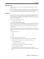
Table of Contents
Before You Begin ........................................................................................................................................
About This Manual .......................................................................................................................................
Guide Contents.......................................................................................................................................
Notational Conventions..........................................................................................................................
Where to Get More Information ...................................................................................................................
1
1
1
2
2
Chapter 1: Product Description ...............................................................................................................
Introducing the ARTIC186 X.25 ISA/PCI Adapter .....................................................................................
Memory Space ..............................................................................................................................................
Programmable Read-Only Memory (PROM)........................................................................................
Dynamic Random-Access Memory .......................................................................................................
80C186 Microprocessor................................................................................................................................
Serial Communications Controller ...............................................................................................................
Counter/Timer and Parallel I/O Unit ............................................................................................................
Watchdog Timer ...........................................................................................................................................
Dual-Port Memory Controller ......................................................................................................................
PCI Target Interface Chip.............................................................................................................................
Communications Capabilities.......................................................................................................................
Support Functions.........................................................................................................................................
5
5
6
6
7
7
7
8
8
8
9
9
9
Chapter 2: Programming Considerations .............................................................................................
Memory and I/O Maps................................................................................................................................
80C186XL Microprocessor ........................................................................................................................
Physical Characteristics .......................................................................................................................
Programming Considerations...............................................................................................................
Interrupt Lines......................................................................................................................................
Interrupt Register Addresses ................................................................................................................
DMA Channel Allocation and Registers..............................................................................................
80C186 Resource Allocation ...............................................................................................................
Peripheral Control Block......................................................................................................................
Memory ................................................................................................................................................
Programmable Read-Only Memory (PROM) ...............................................................................
Dynamic Random-Access Memory (DRAM)...............................................................................
PCI Interface...............................................................................................................................................
Serial EPROM ............................................................................................................................................
PCI-Interface Chip Registers......................................................................................................................
Vendor Identification Register (VID) ..................................................................................................
Device Identification Register (DID)...................................................................................................
PCI Command Register (PCICMD).....................................................................................................
PCI Status Register (PCISTS)..............................................................................................................
Revision Identification Register (RID) ................................................................................................
11
12
12
12
13
13
14
14
15
15
16
16
16
16
17
18
19
20
21
22
23
Table of Contents v
Class Code Register (CLCD) ...............................................................................................................
Cache Line Size Register (CALN).......................................................................................................
Latency Timer Register (LAT) ............................................................................................................
Header Type Register (HDR)...............................................................................................................
Built-in Self-Test Register (BIST) .......................................................................................................
Base Address Registers (BADR0 - 5)..................................................................................................
Subsystem Vendor Identification Register (SVID)..............................................................................
Subsystem Identification Register (SSID) ...........................................................................................
Expansion ROM Base Address Register (XROM)..............................................................................
Interrupt Line Register (INTLN) .........................................................................................................
Interrupt Pin Register (INTPIN) ..........................................................................................................
Minimum Grant Register (MINGNT)..................................................................................................
Maximum Latency Register (MAXLAT) ............................................................................................
AMCC S5920Q Add-On Pass-Thru Address and Data Registers..............................................................
Pass-Thru Address Register Summary.................................................................................................
Pass-Thru Data Register Summary ......................................................................................................
Dual-Port Memory Controller ....................................................................................................................
Physical Characteristics .......................................................................................................................
Performance .........................................................................................................................................
Programming Considerations...............................................................................................................
Register and Command Descriptions...................................................................................................
Memory Mapping.................................................................................................................................
Option Registers...................................................................................................................................
Zilog Z8030 Serial Communications Controller ........................................................................................
Functions ..............................................................................................................................................
SCC Registers ......................................................................................................................................
Write Registers ..............................................................................................................................
Read Registers ...............................................................................................................................
Programming the SCC .........................................................................................................................
Diagnostic Subroutine Support......................................................................................................
PROM Services .............................................................................................................................
Programming Considerations ........................................................................................................
Zilog Z8036 Counter/Timer and Parallel I/O Unit .....................................................................................
Functions ..............................................................................................................................................
CIO Registers .......................................................................................................................................
Programming the CIO ..........................................................................................................................
Diagnostic Subroutines..................................................................................................................
PROM Services .............................................................................................................................
Programming Considerations ........................................................................................................
CIO Port Assignments and Description ...............................................................................................
Watchdog Timer...................................................................................................................................
24
25
26
27
28
29
31
32
33
34
35
36
37
38
38
38
39
40
40
41
41
45
47
48
48
48
49
49
49
49
50
50
50
50
51
52
52
52
52
53
53
Chapter 3: External Interface ................................................................................................................
General Connections...................................................................................................................................
X.21 Interface.......................................................................................................................................
X.21 bis/V.24 Interface (EIA-232) ......................................................................................................
X.21 bis/V.35 Interface ........................................................................................................................
Cables and Connectors ...............................................................................................................................
Cable Identification..............................................................................................................................
D-37 Connector....................................................................................................................................
55
55
57
58
59
60
60
61
vi Artic186 X.25 ISA/PCI Adapter: Technical Reference
X.21 Interface Cable ............................................................................................................................
X.21 bis/V.24 Interface Cable..............................................................................................................
X.21 bis/V.35 Interface Cable..............................................................................................................
Local Loopback-Test Plugs ........................................................................................................................
D-37 Wrap Plug ...................................................................................................................................
D-15 Wrap Plug ...................................................................................................................................
D-25 Wrap Plug ...................................................................................................................................
M/34 Wrap Plug...................................................................................................................................
62
63
64
64
65
65
66
66
Chapter 4: Adapter Characteristics.......................................................................................................
Physical Characteristics ..............................................................................................................................
Adapter Size .........................................................................................................................................
Adapter Technology.............................................................................................................................
Adapter Connectors..............................................................................................................................
Electrical Characteristics......................................................................................................................
Environmental Characteristics .............................................................................................................
Thermal..........................................................................................................................................
Cooling ..........................................................................................................................................
Heat Output....................................................................................................................................
Usability Characteristics ......................................................................................................................
67
67
67
67
67
68
68
68
68
68
68
Chapter 5: PROM Microcode Support .................................................................................................
Support Provided ........................................................................................................................................
Power-On Self-Test ...................................................................................................................................
Errors....................................................................................................................................................
Unrecoverable Errors ...........................................................................................................................
Recoverable Errors...............................................................................................................................
No Errors..............................................................................................................................................
Diagnostic Subroutines...............................................................................................................................
List of Diagnostic Subroutines.............................................................................................................
General Invocation ...............................................................................................................................
General Error Handling........................................................................................................................
Test DRAM Subroutine .......................................................................................................................
Checksum Subroutine ..........................................................................................................................
Get Memory Size Subroutine...............................................................................................................
Test Microprocessor Subroutine ..........................................................................................................
Test CIO Subroutine ............................................................................................................................
Test SCC Subroutine............................................................................................................................
Test Dual-Port Memory Controller Subroutine ...................................................................................
Get Communications Port Identity Subroutine ....................................................................................
Configure CIO Port Subroutine ...........................................................................................................
Configure SCC Port Subroutine...........................................................................................................
Configure DMA Channel Subroutine ..................................................................................................
Configure CIO Timers Subroutine.......................................................................................................
Configure Watchdog Timer Subroutine...............................................................................................
Switch Interrupt Priorities Subroutine .................................................................................................
Get X.25 Electrical Interface Assembly Identifier Subroutine ............................................................
Get Base Card ID Subroutine...............................................................................................................
PROM Services ..........................................................................................................................................
General Invocation ...............................................................................................................................
69
69
69
70
70
71
71
74
74
74
74
75
76
77
78
79
80
81
82
83
85
87
89
90
92
93
94
95
95
Table of Contents vii
List of PROM Services ........................................................................................................................ 95
Interrupt System Unit Subroutine ........................................................................................................ 96
Reset an SCC Port Subroutine ............................................................................................................. 97
Access SCC Registers Subroutine ....................................................................................................... 98
Access CIO Registers Subroutine ...................................................................................................... 100
CIO Timer Support Subroutine.......................................................................................................... 102
Connect DMA Channel(s) Subroutine ............................................................................................... 104
Set Up and Start DMA Channel Subroutine ...................................................................................... 106
Access DMA Channel Registers Subroutine ..................................................................................... 109
Stop DMA Channel Subroutine ......................................................................................................... 111
Convert Logical to Physical Address Subroutine .............................................................................. 112
Convert Segment to Page Subroutine ................................................................................................ 113
Convert Page to Segment Subroutine ................................................................................................ 114
Pointer to EBCDIC-ASCII Tables ..................................................................................................... 115
Convert EBCDIC String to ASCII Subroutine .................................................................................. 116
Convert ASCII String to EBCDIC Subroutine .................................................................................. 117
Add Element to Intrasegment Ring Subroutine ................................................................................. 118
Remove Element From Intrasegment Ring Subroutine ..................................................................... 119
Add Element to Intersegment Ring Subroutine ................................................................................. 120
Remove Element From Intersegment Ring Subroutine ..................................................................... 121
Bootstrap Loader Subroutine.................................................................................................................... 122
Dump Facility ........................................................................................................................................... 122
Dump1 Subroutine ............................................................................................................................. 123
Dump2 Subroutine ............................................................................................................................. 124
Appendix A: Dual-Port Memory Controller.......................................................................................
Design Changes ........................................................................................................................................
Design Methodology and Technology ..............................................................................................
Bus Interface Descriptions .................................................................................................................
80186-Bus Interface ...........................................................................................................................
DRAM-Bus Interface .........................................................................................................................
ISA-Bus Interface...............................................................................................................................
Resets .................................................................................................................................................
Dual-Port Memory Controller FPLD Registers........................................................................................
Control-Alt-Delete Registers (CAD2, CAD1, CAD0) ......................................................................
Command Register (COMREG) ........................................................................................................
CPU Page Register (CPUPG) ............................................................................................................
Data Register (DREG) .......................................................................................................................
Gate Array Identification (GAID)......................................................................................................
Internal DMA Allocation Register (IDAL)........................................................................................
Initialization Register 0 (INITREG0) ................................................................................................
Initialization Register 1 (INITREG1) ................................................................................................
Initialization Register 2 (INITREG2) ................................................................................................
Location Registers (LOCREG1, LOCREG0) ....................................................................................
NMI Mask Register (NMIMASK).....................................................................................................
NMI Status Register (NMISTAT) .....................................................................................................
Option Register 0 (OPTION0) ...........................................................................................................
Option Register 1 (OPTION1) ...........................................................................................................
Pointer Register (PTRREG)...............................................................................................................
Task Register (TREG)........................................................................................................................
viii Artic186 X.25 ISA/PCI Adapter: Technical Reference
125
125
127
127
129
129
130
132
133
134
135
137
138
139
140
142
144
146
147
149
151
152
154
155
156
Dual-Port Memory Controller FPLD Commands ....................................................................................
General End Of Interrupt Command (GEOI).....................................................................................
Interrupt Command (INTCOM).........................................................................................................
Interrupt Sharing Enable Command (ISEC) ......................................................................................
I/O Signals ................................................................................................................................................
Packaging and Pin Information ................................................................................................................
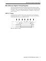
Miscellaneous Signals Timing Diagrams .................................................................................................
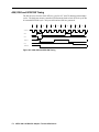
AR(15:1) Timing................................................................................................................................
AS#, CSn, RDIDnn#, R/W#, and SRDY Timing ..............................................................................
DRQn Timing.....................................................................................................................................
AS#, DS# and INTA1R# Timing.......................................................................................................
Dual-Port Memory Controller FPLD’s Miscellaneous Glue Control Signals..........................................
157
158
159
160
161
168
173
173
174
175
176
177
Appendix B: Configuration ..................................................................................................................
Creating an ICAPARM.PRM File............................................................................................................
Example 1 – For One Co-Processor Adapter.....................................................................................
Example 2 – For Multiple Co-Processor Adapters ............................................................................
Changing Your CONFIG.SYS File ..........................................................................................................
Ctrl-Alt-Del Reset Considerations............................................................................................................
179
179
179
180
180
180
Appendix C: Communications .............................................................................................................
Concepts of Packet-Switched Data Networks ..........................................................................................
DSEs, DTEs, and DCEs .....................................................................................................................
Levels of X.25 ..........................................................................................................................................
Physical Level ....................................................................................................................................
Link Level ..........................................................................................................................................
Packet Level .......................................................................................................................................
Data Packets .......................................................................................................................................
Logical Channels ......................................................................................................................................
Types of Logical Channels .......................................................................................................................
181
181
181
182
183
183
185
187
188
188
Glossary ................................................................................................................................................... 191
Index......................................................................................................................................................... 199
Table of Contents ix
x Artic186 X.25 ISA/PCI Adapter: Technical Reference
Figures
1-1. Block Diagram of the ARTIC186 X.25 ISA/PCI Adapter Co-Processor .......................................... 6
2-1. PCI Configuration Space Header ..................................................................................................... 18
3-1. Connecting the Adapter to an X.25 Public Packet-Switched Network ............................................ 55
3-2. X.21 Interface Control...................................................................................................................... 57
3-3. X.21 bis/V.24 Interface Control ....................................................................................................... 58
3-4. X.21 bis/V.35 Interface Control ....................................................................................................... 59
3-5. Cable ID (X.21 bis/V.24 Interface Cable Connected)...................................................................... 60
3-6. X.25 Network Interface Connector .................................................................................................. 61
3-7. X.21 Interface Cable......................................................................................................................... 62
3-8. X.21 Bis/V.24 Interface Cable ......................................................................................................... 63
3-9. X.21 Bis/V.35 Interface Cable ......................................................................................................... 64
3-10. D-37 Wrap Plug Pin Assignment ................................................................................................... 65
3-11. D-15 Wrap Plug Pin Assignment ................................................................................................... 65
3-12. D-25 Wrap Plug Pin Assignment ................................................................................................... 66
3-13. M/34 Wrap Plug Pin Assignment................................................................................................... 66
4-1. ARTIC186 X.25 ISA/PCI Adapter .................................................................................................. 67
5-1. PROM Error Counters...................................................................................................................... 73
A-1. Dual-Port Memory Controller FPLD-Bus Interfaces .................................................................... 128
A-2. Mapping DRAM into ISA Memory-Address Space ..................................................................... 131
A-3. AR(15:1) Timing ........................................................................................................................... 173
A-4. AS#, CSn, RDIDnn#, R/W# and SRDY Timing........................................................................... 174
A-5. DRQn Gating by Dual-Port Memory Controller FPLD ................................................................ 175
A-6. AS#, DS# and INTA1R# Timing .................................................................................................. 176
A-7. ABT543 Wiring............................................................................................................................. 177
C-1. Elements of a Packet-Switched Data Network .............................................................................. 182
C-2. Control Byte (Modulo 8) ............................................................................................................... 184
C-3. General Pack Format ..................................................................................................................... 185
C-4. Establishing a Switched Virtual Circuit ........................................................................................ 186
C-5. Clearing a Switched Virtual Circuit .............................................................................................. 186
C-6. DTE Initiated Reset ....................................................................................................................... 186
C-7. DCE Initiated Reset ....................................................................................................................... 186
C-8. Data Packet with Modulo 8 ........................................................................................................... 187
C-9. Data Packet with Modulo 128 ....................................................................................................... 187
Figures xi
xii Artic186 X.25 ISA/PCI Adapter: Technical Reference
Tables
2-1. 80C186 Memory Map ....................................................................................................................... 12
2-2. 80C186 I/O Map................................................................................................................................ 12
2-3. Interrupt Controller Register Model.................................................................................................. 14
2-4. DMA Register Addresses.................................................................................................................. 15
2-5. 80C186 Microprocessor Interrupts.................................................................................................... 15
2-6. 80C186 Microprocessor Counter/Timers.......................................................................................... 15
2-7. 80C186 Microprocessor DMA Channels .......................................................................................... 15
2-8. Z8036 CIO Timers ............................................................................................................................ 15
2-9. Peripheral Interface Register Addresses............................................................................................ 16
2-10. EEPROM Values ............................................................................................................................ 17
2-11. Register Addresses and Initial Values............................................................................................. 42
2-12. Command Addresses and Initial Values ......................................................................................... 43
2-13. SCC Write Register Addresses and Usage...................................................................................... 49
2-14. SCC Read Register Addresses and Usage....................................................................................... 49
2-15. Diagnostic Subroutines.................................................................................................................... 49
2-16. PROM Services ............................................................................................................................... 50
2-17. CIO Main Control Registers............................................................................................................ 51
2-18. Frequently Accessed Registers of the CIO...................................................................................... 51
2-19. CIO Counter/Timer Registers ......................................................................................................... 51
2-20. CIO Port 0 Specification Registers ................................................................................................. 52
2-21. CIO Port 0 Specification Register ................................................................................................... 52
2-22. Diagnostic Subroutines.................................................................................................................... 52
2-23. PROM Services ............................................................................................................................... 52
2-24. CIO Bit Assignments, Port 0........................................................................................................... 53
2-25. CIO Bit Assignments, Port 1........................................................................................................... 53
2-26. LED Operation ................................................................................................................................ 54
2-27. Watchdog Timer Description .......................................................................................................... 54
3-1. Cable and Wrap Plug Identification .................................................................................................. 60
4-1. Power Requirements.......................................................................................................................... 68
4-2. Environmental Classification Ratings ............................................................................................... 68
5-1. POST Error Codes............................................................................................................................. 71
5-2. POST Error Codes ............................................................................................................................ 71
5-3. CIO Port Registers............................................................................................................................. 83
5-4. CIO Timers........................................................................................................................................ 89
5-5. Watchdog Timer................................................................................................................................ 90
5-6. Port 2 Registers ................................................................................................................................. 90
A-1. Memory Access Wait States with 14.74 MHz CLKIN .................................................................. 130
A-2. Memory Access Wait States with 20 MHz CLKIN ....................................................................... 130
A-3. Memory Access Wait States with 25 MHz–29.49 MHz CLKIN ................................................... 130
A-4. Register Names and Addresses ...................................................................................................... 133
A-5. Input Signals ENPCI, C8, C4, C2, C1, and Base I/O Addresses ................................................... 142
Tables xiii
A-6. Input Signals L4, L2, and L1..........................................................................................................
A-7. ENPCI, ED, LOCREG1, BW, and Data-Bus Width Addressing...................................................
A-8. Input Signals C8, C4, C2, C1, and Base I/O Addresses.................................................................
A-9. Input Signals L4, L2, and L1..........................................................................................................
A-10. Pointer Register Values ................................................................................................................
A-11. Dual-Port Memory Controller FPLD Commands ........................................................................
A-12. Dual-Port Memory Controller ISA-Bus Interface Signals ..........................................................
A-13. Dual-Port Memory Controller 80186-Bus Interface Signals .......................................................
A-14. Dual-Port Memory Controller DRAM-Bus Interface Signals......................................................
A-15. Dual-Port Memory Controller Miscellaneous Signals ................................................................
A-16. Signals and Physical Pin Number ................................................................................................
xiv Artic186 X.25 ISA/PCI Adapter: Technical Reference
143
145
152
153
155
157
161
162
163
164
168
Before You Begin
This technical reference manual describes the ARTIC186 X.25 ISA/PCI Adapter.
The reader is assumed to have some knowledge of telecommunication protocols, although
an introduction to X.25 packet-switched data networks is contained in Appendix C.
About This Manual
The information in this publication is both introductory and reference. It is intended for
hardware and software designers, programmers, engineers, and those with a knowledge of
electronics and/or programming who need to understand the operation of the ARTIC186
X.25 ISA/PCI Adapter.
The ARTIC186 X.25 ISA/PCI Adapter is the combination of the popular X.25 ISA and the
X.25 PCI Adapters.
This dual adapter plugs into a single I/O slot in PCI or ISA compliant systems, allowing
complete compatibility with existing applications running on the two current X.25
Adapters. It also allows the system unit to communicate over an X.25 packet-switched
network. The adapter has its own microprocessor and memory, thus allowing it to carry
out most of the communications work that would otherwise be done by the system unit.
Guide Contents
Chapter
1 Product Description
2
Programming Considerations
3
External Interface
4
Adapter Characteristics
5
PROM Microcode Support
Description
This chapter describes the adapter hardware and how it
operates; it also relates the adapter to other IBM
communications co-processors.
This chapter provides programming considerations and a
detailed description of the adapter microprocessor, PCI
interface, dual-port memory controller, serial
communications controller, and counter/timer and parallel
I/O unit.
This chapter describes the network interface, covering
details about the X.21 interface, the X.21 bis/V.24
interface, and the X.21 bis/V.35 interface.
This chapter describes the physical and electrical
characteristics of the adapter.
This chapter describes the power-on self-test and all the
support subroutines resident in the adapter PROM.
Before You Begin 1
Appendixes
The appendices provide additional information about the ARTIC186 X.25 ISA/PCI
Adapter.
Appendix
A Dual-Port Memory Controller
B Configuration
C Communications
Glossary
Description
This appendix contains information about the dual-port
memory controller design changes, bus interface
descriptions, FPLD commands, and register details.
This appendix contains information about special
considerations needed when configuring and operating a
system with the adapter installed.
This appendix provides an overview of X.25 packetswitched networks.
This section contains definitions of special terms and
abbreviations used in this manual.
Notational Conventions
This manual uses the following conventions:
•
Nondecimal numbers are represented with a trailing letter, such as an h or b. The
trailing h identifies the number as a hexadecimal value; the trailing b identifies the
number as a binary value. Numbers without a trailing letter are assumed to be decimal
values.
•
Bit 0 is the low-order bit. If a bit is set to 1, the associated description is true unless
otherwise stated.
•
KB = 1024 bytes
•
MB = 1,048,576 bytes
•
Data structures and syntax strings appear in this typeface.
Where to Get More Information
One or more of the following publications might be needed for reference when using this
technical reference manual:
IBM Disk Operating System (DOS), Version 3.3 or later
IBM Macro Assembler, Version 2.0 or IBM Macro Assembler/2
IBM Operating System/2(TM) (OS/2(TM)), Version 2.0 or later (Standard or Extended Edition)
The technical reference manual for your system unit
Intel iAPX 86/88, 186/188: User’s Manual Hardware Reference
Intel 80C186/C188 80C186XL/C188XL Microprocessor User’s Manual, 272164
PCI Local Bus Specification, Revision 2.1, June 1, 1995
AMCC S5920Q Databook, Section 2, 1998
Zilog Serial Communications Controllers Databook, DC 8316
2 ARTIC186 X.25 ISA/PCI Adapter: Technical Reference
Where to Get More Information
Zilog 8030/Z8530 Serial Communications Controller Technical Manual
Zilog Z8036 CIO Counter/Timer and Parallel I/O Unit Technical Manual, 00-2091
ARTIC OS/2 Support User’s Guide
ARTIC DOS Support User’s Guide
ARTIC Dual-Port, ARTIC Multiport, and ARTIC Multiport/2 Technical Reference
ETSI Standards:
NET 1 - Approval requirements for data terminal equipment to connect to circuit switched
public data networks and leased circuits using CCITT Recommendation X.21 interface
NET 2 - Approval requirements for data terminal equipment to connect to packet switched
public data networks using CCITT Recommendation X.25 interface
CCITT Blue Book, Recommendations:
X.1 - International user classes of service in public data networks and integrated services
digital networks (ISDNs)
X.21 - Interface between data terminal equipment (DTE) and data circuit-terminating
equipment (DCE) for synchronous operation on public data networks
X.21 bis - Use on public data networks of data terminal equipment (DTE) which is
designed for interfacing to synchronous V-Series modems
X.25 - Interface between data terminal equipment (DTE) and data circuit-terminating
equipment (DCE) for terminals operating in the packet mode and connected to public data
networks by dedicated circuit
X.28 - DTE/DCE interface for a start-stop mode data terminal equipment accessing the
packet assembly/disassembly facility (PAD) in a public data network situated in the same
country
X.150 - Principles of maintenance testing for public data networks using data terminal
equipment (DTE) and data circuit-terminating equipment (DCE) test loops
V.10 - Electrical characteristics for unbalanced double-current interchange circuits for general use with integrated circuit equipment in the field of data communications
V.24 - List of definitions for interchange circuits between data terminal equipment (DTE)
and data circuit-terminating equipment (DCE)
V.28 - Electrical characteristics for unbalanced double-current interchange circuits
ANSI and EIA Standards:
ANSI/EIA/TIA-232-E - Interface Between Data Terminal Equipment and Data Circuit-Terminating Equipment Employing Serial Binary Data Interchange
EIA-422-A - Electrical Characteristics of Balanced Voltage Digital Interface Circuits
EIA-423-A - Electrical Characteristics of Unbalanced Voltage Digital Interface Circuits
Before You Begin 3
ISO Standards:
ISO 2110 - Information Technology - Data Communication - 25-Pole DTE/DCE Interface
Connector and Contact Number Assignments
ISO 4903 - Data Communication - 15-pin DTE/DCE Interface Connector and Pin Assignments
X.25 Interface for Attaching SNA Nodes to Packet-Switched Data Networks, General
Information Manual, GA27-3345
X.25 Interface for Attaching IBM SNA Nodes to Packet-Switched Data Networks, General
Information, SC30-3409
Safety Standards:
Underwriters’ Laboratory Specification UL2943
Underwriters’ Laboratory Specification UL2464
4 ARTIC186 X.25 ISA/PCI Adapter: Technical Reference
Chapter
1
1
Product Description
This chapter describes the ARTIC186 X.25 ISA/PCI Adapter hardware and how it
operates.
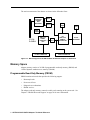
Introducing the ARTIC186 X.25 ISA/PCI Adapter
The ARTIC186 X.25 ISA/PCI Adapter is a single-slot, half-card adapter for use in PCI or
ISA interface bus compliant systems. The adapter contains:
•
1 MB of dynamic random-access memory (DRAM)
•
16 KB of programmable read-only memory (PROM)
•
An 80C186-20 microprocessor
•
A serial communications controller (SCC)
•
A counter/timer and parallel I/O unit (CIO)
•
A dual-port memory controller
•
AMCC S5920Q PCI Target Interface chip (AMCC)
•
Interface line drivers and receivers to support the X.25 layer
Chapter 1: Product Description 5
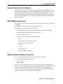
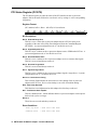
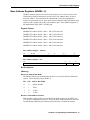
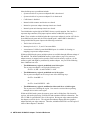
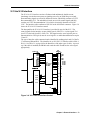
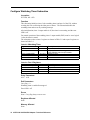
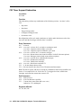
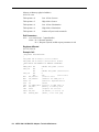
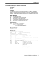
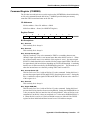
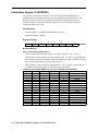
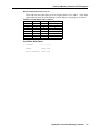
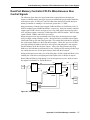
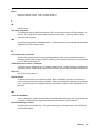
The major components of the adapter are shown in the following figure.
INTERFACE
DRIVERS
AND
RECEIVERS
CIO
Z8036
SCC
Z8030
1 MB
DRAM
PROM
SERIAL
EPROM
37-PIN
D-SHELL
AMCC PCI
TARGET
INTERFACE
CHIP
MACH
CHIP
PCI BUS CONNECTOR
ISA
DUAL-PORT
MEMORY
CONTROLLER
80C186
PROCESSOR
ISA BUS CONNECTOR
Figure 1-1. Block Diagram of the ARTIC186 X.25 ISA/PCI Adapter Co-Processor
Memory Space
Adapter memory consists of 16 KB of programmable read-only memory (PROM) and
1 MB of dynamic random-access memory (DRAM).
Programmable Read-Only Memory (PROM)
PROM contains microcode that provides the following support:
•
Bootstrap loader
•
Power-on self-test
•
Diagnostic test subroutines
•
PROM services.
The adapter read-only memory cannot be read by tasks running on the system unit. See
Chapter 5 "PROM Microcode Support" on page 69 for more information.
6 ARTIC186 X.25 ISA/PCI Adapter: Technical Reference
80C186 Microprocessor
Dynamic Random-Access Memory
Tasks running on the 80C186 microprocessor can access all 1 MB of DRAM. Tasks
running on the system unit can access adapter DRAM through an 8 KB memory window.
The window starts on an 8 KB boundary. Although not recommended, the size and
location of this shared storage window can be dynamically changed by tasks running on
the system unit and the adapter. The window is controlled by registers in the dual-port
memory controller.
80C186 Microprocessor
Processing power is provided by an 80C186XL microprocessor running at 7.37MHz or
14.32MHz.
A switch on the card selects the processor operating speed.
The microprocessor can be used for the following:
•
Communications-related processing (relieving the system unit of this burden)
•
Preparing and processing inbound and outbound data
•
Processing of application tasks
•
Control of memory and peripheral chips, including:
–
Timers
–
Direct memory access (DMA) channels
–
Serial communication controller
–
Counters
–
I/O ports
–
Parallel I/O unit
–
Dual-port memory controller
Serial Communications Controller
The serial communications controller (SCC) provides the following:
•
Two independent full-duplex channels
•
HDLC support
•
DMA capability
The SCC provides bit-transparency and error detection for the X.25 communications
interfaces. After being initialized by the Realtime Control Microcode (RCM) and support
software, the SCC performs a major portion of the X.25 level-1 communications
workload. Before it can perform X.25 functions, an application must be loaded on the
adapter. Application code is not shipped with this adapter.
Chapter 1: Product Description 7
Counter/Timer and Parallel I/O Unit
The counter/timer and parallel I/O unit (CIO) provides the following:
•
Three independent 16-bit timers
•
Two independent, 8-bit, double-buffered, bidirectional I/O ports
•
A special purpose, 4-bit I/O port
The two 8-bit ports are used to control the flow of data through the X.25 interfaces. The
watchdog timer uses one timer and the 4-bit I/O port. The remaining two 16-bit timers are
available for user tasks.
Watchdog Timer
After the watchdog timer is activated, it counts down towards zero and must be
continually monitored by software to prevent reaching zero. If the watchdog timer
actually does reach zero, the CIO does the following:
•
Lights a light-emitting-diode (LED) on the edge of the adapter
•
Sends an interrupt to the 80C186 microprocessor
•
Sends an interrupt to the system unit
Dual-Port Memory Controller
The dual-port memory controller is an IBM CMOS gate array with 10000 gates that
provides a convenient and flexible way of passing data and control bytes between the
80C186 bus and the system unit bus. The chip adapts to both 8-bit and 16-bit data buses
on the system bus. The basic purpose of the VLSI gate array is to provide a highperformance interface between the co-processor adapter and the system. All data
communications between the system and the co-processor adapter go through this
interface. The dual-port memory controller provides this communication using the
following functions:
•
8 KB Page Selection from the system
•
Interrupt Handling
•
Watchdog Timer Errors
•
Initialization Conditions
•
System Unit Lost Refresh Condition
See “Dual-Port Memory Controller” on page 39 for more information.
8 ARTIC186 X.25 ISA/PCI Adapter: Technical Reference
PCI Target Interface Chip
PCI Target Interface Chip
The AMCC S5920Q chip provides all the function needed by the ARTIC186 X.25 ISA/
PCI Adapter to interface to the PCI bus. The PCI Target Interface Chip provides three
physical bus interfaces:
•
PCI bus
•
ISA bus (interface to the dual-port memory controller)
•
Optional external non-volatile memory
Communications Capabilities
The adapter provides any one of the following X.25 interfaces (see Chapter 3. "External
Interface" on page 55 for more information):
•
X.21
•
X.21 bis/V.24 (RS-232)
•
X.21 bis/V.35
The adapter provides direct memory access (DMA) between adapter memory and the
serial communications controller (SCC) channels.
The adapter hardware provides no specific X.25 protocol function, other than HDLC. The
X.25 packet level must be provided by application software running on the adapter.
Support Functions
The adapter provides the following support functions through the PROM microcode and
the RCM:
•
Multiple task management for up to 253 tasks with priorities
•
Interface functions between the adapter and the system unit
•
First-level interrupt handlers
•
Diagnostic subroutines
•
Bootstrap loader
•
Resource management for:
–
User queues
–
Memory
–
Hardware timers
–
Software timers
–
Communications ports
–
DMA channels
–
Interrupt vectors
Chapter 1: Product Description 9
10 ARTIC186 X.25 ISA/PCI Adapter: Technical Reference
Chapter
2
Programming Considerations
2
This chapter describes the individual components of the ARTIC186 X.25 ISA/PCI
Adapter Co-Processor. A block diagram of the adapter is in Figure 1-1 on page 6. Each
major component is described in terms of its function, physical characteristics, and special
features. Programming information is provided, or referenced, for those components that
are programmable.
Applications can use this information to directly program the hardware or they can
selectively use the supplied support packages. Available programming support includes:
•
Operating system device drivers
•
On-card realtime operating system
•
On-card communications support
•
Programming language support
Operating System Device Drivers:
•
ARTIC DOS Support
•
ARTIC OS/2 Support
•
ARTIC NT Support
•
ARTIC WIN98 Support
•
ARTIC AIX Support
ARTIC186 Microcode:
•
Realtime Control Microcode (RCM)
On-Card Communications WAN Support:
•
Realtime Interface Co-Processor Extended Services
Programming Language Support:
•
Realtime Interface Co-Processor C Language Support
•
Realtime Interface Co-Processor Developer’s Kit
Chapter 2: Programming Considerations 11
Memory and I/O Maps
The 80C186 memory map is shown in the following table.
Table 2-1. 80C186 Memory Map
Address
Size
Use
FC000–FFFFFh
16 KB
80C186 '-UCS' - PROM
F0000–FBFFFh
48 KB
80C186 '-UCS' - PROM (Shadow)
00000–EFFFFh
960 KB
DRAM
Note: -UCS is the Upper Memory Chip Select on the 80C186.
The I/O map is shown in the following table.
Table 2-2. 80C186 I/O Map
I/O Address
Size
FF00–FFFFh
256 Bytes
0900–FEFFh
61.5 KB
0800–08FFh
256 Bytes
0700–07FFh
256 Bytes
0600–06FFh
256 Bytes
0500–05FFh
256 Bytes
0400–04FFh
256 Bytes
0282–03FFh
126 Bytes
0280–0281h
2 Bytes
0202–027Fh
126 Bytes
0200–0201h
2 Bytes
0180–01FFh
128 Bytes
0100–017Fh
128 Bytes
00F8–00FFh
8 Bytes
0088–00F7h
112 Bytes
0084–0087h
4 Bytes
0080–0083h
4 Bytes
001A–007Fh
102 Bytes
0000–0019h
26 Bytes
Use
80C186 PCB
Reserved
Dual-Port Memory Controller Select 8
Dual-Port Memory Controller Select 7
Dual-Port Memory Controller Select 6
Dual-Port Memory Controller Select 5
Dual-Port Memory Controller Select 4
Reserved
Reserved
Reserved
Reserved
Dual-Port Memory Controller Select 2 - CIO0
Dual-Port Memory Controller Select 1 - SCC
80187 decode - Reserved
Reserved
Dual-Port Memory Controller registers
Dual-Port Memory Controller registers
Reserved
Dual-Port Memory Controller registers
PROM and DRAM do not require wait states but are programmed by the RCM to accept
an external ready line controlled by the dual-port memory controller. All peripheral
devices are programmed for one wait state and to accept an external ready.
80C186XL Microprocessor
Physical Characteristics
The main features of the 80C186XL microprocessor are:
•
16-bit architecture
•
7.3728 MHz and 14.32 MHz operating frequencies
•
Typical 542.4-nanosecond bus cycle time (0 wait states)
•
Maximum 814-nanosecond bus cycle time (2 wait states)
•
Three programmable 16-bit timers (reserved for the Realtime Control Microcode)
12 ARTIC186 X.25 ISA/PCI Adapter: Technical Reference
80C186XL Microprocessor
•
Internal programmable interrupt controller
•
Internal clock generator
•
Two independent high-speed DMA channels
•
Storage and peripheral chip selects
•
Internal programmable wait state generator
•
16-bit data bus
•
20-bit address bus
•
Twice the performance of the 8086 microprocessor
Programming Considerations
Programming of the 80C186 microprocessor is described in detail in the Intel literature.
This section deals with special considerations when programming the 80C186
microprocessor for the ARTIC186 X.25 ISA/PCI Adapter.
Interrupt Lines
The 80C186 microprocessor has five interrupt lines; only NMI, INT0, and INT1 are used.
NMI and INT0 are driven by the dual-port memory controller. INT1 is driven by the SCC
and CIO. Nonmaskable interrupts can be masked by appropriately setting the NMIMASK
register in the dual-port memory controller.
The dual-port memory controller issues edge-triggered interrupts on INT0 in fully nested
mode. The SCC and CIO issue level-triggered interrupts on INT1 in cascade mode.
The interrupt vectors for NMI and INT0 are provided internally by the 80C186
microprocessor. The interrupt vectors for INT1 are provided by the Zilog Z8030 Serial
Communications Controller and the Zilog Z8036 Counter/Timer and Parallel I/O unit.
The SCC and CIO select which device supplies the vector during the interrupt
acknowledgment cycle. The SCC has a higher interrupt priority than the CIO.
After a hardware interrupt, the nonspecific end-of-interrupt (EOI) command, 8000h, must
be written to the EOI register to re-enable interrupts. Interrupts are enabled at the same or
lower priority as the previous interrupt.
EOI is the only command a task should issue to the interrupt controller. Any other
command or change could cause unpredictable results.
Example:
MOV
AX,08000h ;data value for nonspecific EOI
MOV
DX,0FF22h ;I/O address of EOI register
OUT
DX,AX
;Issue EOI
Chapter 2: Programming Considerations 13
Interrupt Register Addresses
The 15 interrupt controller registers are shown in the following table.
Table 2-3. Interrupt Controller Register Model
Register
Address
INT3 control register
FF3Eh
INT2 control register
FF3Ch
INT1 control register
FF3Ah
INT0 control register
FF38h
DMA1 control register
FF36h
DMA0 control register
FF34h
Timer control register
FF32h
Interrupt status register
FF30h
Interrupt request register
FF2Eh
In-service register
FF2Ch
Priority mask register
FF2Ah
Mask register
FF28h
Poll status register
FF26h
Poll register
FF24h
EOI register
FF22h
DMA Channel Allocation and Registers
The 80C186 microprocessor has two integral DMA channels. The registers that control
them are described in Table 2-4 on page 15 and in the Intel literature. The adapter uses a
DMA steering multiplexer to allocate the DMA channels to the following four potential
requesting sources:
•
SCC port 0 transmitter (TxREQA)
•
SCC port 1 transmitter (TxREQB)
•
SCC port 0 receiver (RxREQA)
•
SCC port 1 receiver (RxREQB)
Tasks running on the adapter can write to and read from the internal DMA allocation logic
register (IDAL). See “Internal DMA Allocation Register (IDAL)” on page 140 for more
information.
When using DMA, first enable the SCC through its WR0 register, then enable the DMA
channel through the DMA control word register.
The DMA allocation logic register (IDAL) and the 80C186 microprocessor DMA
registers are set by the Connect DMA Channels PROM service subroutine (INT AAh).
See “Connect DMA Channel(s) Subroutine” on page 104 for more information.
The DMA registers for DMA channel 0 are located at FFC0h through FFCAh and for
DMA channel 1 at FFD0h through FFDAh. The DMA controller registers are shown in
Table 2-4 on page 15. PROM Services subroutines can be used to program the DMA so
that the DMA control registers do not have to be accessed directly.
14 ARTIC186 X.25 ISA/PCI Adapter: Technical Reference
80C186XL Microprocessor
Table 2-4. DMA Register Addresses
Register Name
Control word
Transfer count
Destination pointer (high)
Destination pointer (low)
Source pointer (high)
Source pointer (low)
Address Channel 0 Address Channel 1
FFCAh
FFDAh
FFC8h
FFD8h
FFC6h
FFD6h
FFC4h
FFD4h
FFC2h
FFD2h
FFC0h
FFD0h
80C186 Resource Allocation
The following tables show how the various 80C186 resources are allocated.
Table 2-5. 80C186 Microprocessor Interrupts
Signal
Pin No. Assignment
NMI
46
Parity error, watchdog, NMI command, lost refresh, parity channel
check, Ctrl-Alt-Del
INT0
45
Dual-port memory controller
INT1
44
SCC and CIO
INT2
42
Reserved
INT3
41
Interrupt acknowledge for SCC and CIO
Table 2-6. 80C186 Microprocessor Counter/Timers
Signal
Pin No. Assignment
TIMER0
20
For RCM use, offset 50h–56h
TIMER1
21
For RCM use, offset 58h–5Eh
TIMER2
For RCM use, offset 60h–66h
Table 2-7. 80C186 Microprocessor DMA Channels
Signal
Pin No.
Assignment
DRQ0
18
Allocated by user task running on adapter, offset C0–CAh
DRQ1
19
Allocated by user task running on adapter, offset D0–DAh
Table 2-8. Z8036 CIO Timers
Signal
Pin No. Assignment
TIMER1
14
Available for user tasks via RCM
TIMER2
10
Available for user tasks via RCM
TIMER3
21
Watchdog
Peripheral Control Block
The 80C186 microprocessor peripheral control block is set up by the power-on
diagnostics. It is located in adapter I/O space at address FF00h through FFFFh. The only
areas of the peripheral control block that should be modified are the DMA descriptors and
interrupt controller registers described on page 14. Modifying any other register can cause
unpredictable results.
Chapter 2: Programming Considerations 15
Memory
PROM and DRAM do not require wait states but are programmed by the RCM to accept
an external ready line controlled by the dual-port memory controller. All peripheral
devices are programmed for one wait state and to accept an external ready. The peripheral
interface register addresses are shown in the following table.
Table 2-9. Peripheral Interface Register Addresses
Register
Address
UMCS
FFA0h
LMCS
FFA2h
PACS
FFA4h
MMCS
FFA6h
MPCS
FFA8h
Programmable Read-Only Memory (PROM)
16 KB of programmable read-only memory (PROM) contains the PROM microcode
which is accessed by the 80C186 on the ARTIC186 X.25 ISA/PCI Adapter. The PROM is
not accessible by the system unit.
Programmable read-only memory is provided by two 32-pin 27C256 devices. Each
device provides 8 KB of storage with an access time of 200 nanoseconds. Memory
decoding of the PROM area is handled by the 80C186 through the -UCS (upper memory
chip select) output, which is programmed to a decode range of 64 KB by writing a value of
F038h to the UMCS register in the PCB.
A power-on self-test (POST) is included in the PROM microcode. POST performs a
checksum verification on PROM. A user task can also call the checksum diagnostic
subroutine at any time. A list of the functions performed during POST is shown in
“Power-On Self-Test” on page 69.
Dynamic Random-Access Memory (DRAM)
The dual-port memory controller guarantees a DRAM cycle time of 250 nanoseconds.
This implies a maximum data transfer rate of 8 Mbps, but the microprocessor cannot
access DRAM at this rate. Each access holds DRAM for 250 nanoseconds before
releasing it and making it available for another access.
DRAM consists of one 4 MB x 16-bit 50-pin SOIC package with 50 nanosecond access
time. The 1 MB of DRAM is organized as 512K 16-bit words.
The DRAM is accessed as a 16-bit device by the 80C186 microprocessor, as an 8-bit or
16-bit device by the system unit and as an 8-bit device by on-card DMA.
The power-on self-test (POST) checks DRAM for size, addressability, and parity. The
PROM microcode test subroutines may also be called at any time by user tasks running on
the adapter. See “Power-On Self-Test” on page 69 for details.
PCI Interface
The PCI interface on the ARTIC186 X.25 ISA/PCI Adapter is implemented with an
AMCC S5920Q PCI Target interface chip. The interface complies with Revision 2.1 of
the PCI Local Bus Specification with the following exceptions:
16 ARTIC186 X.25 ISA/PCI Adapter: Technical Reference
Serial EPROM
•
On burst reads to the card, the card terminates the cycle by activating the STOP#
signal in the clock cycle after the first data phase. This violates rule 4 under section
3.3.3.2.1 of the PCI Specification, which states that after a target asserts TRDY# or
STOP# it cannot change DEVSEL#, TRDY#, or STOP# until the current data phase
completes.
•
The card does not terminate cycles as specified in section 3.3.3.3 of the PCI
Specification because the timers have been disabled in the AMCC S5920Q chip
through bit 0 of EPROM location 45 to fix a bus hang found in some PCI systems.
Each PCI-bus device contains a unique 256-byte configuration header-space region.
Portions of this configuration header are mandatory for a PCI card to be in full compliance
with the PCI Specification. The following section describes each of these configuration
registers including its address, default values, initialization options, and bit definitions.
According to the PCI specification, care must be exercised with registers that have
reserved bits to make sure they are handled correctly. On reads, software must use
appropriate masks to extract defined bits, and might not rely on reserved bits being any
particular value. On writes, software must ensure that the values of the reserved bit
positions are preserved by first reading the values of these bits and then writing these
values back when writing the new values of other bit positions.
Serial EPROM
A serial EPROM interface of three pins is provided to allow automatic configuration of
the PCI-interface chip.
The serial EPROM interface is a Microchip 24LC02B 2K bits (1 block of 256x8 bits)
EEPROM. Values must be programmed into this chip with the format specified in the
following table.
EPROM Values
Table 2-10. EEPROM Values
Offset
Description
00–3Fh
unused
40–41h
Vendor ID
42–43h
Device ID
44h
unused
45h
Target Latency Timer (bit 0)
46–47h
unused
48h
Revision ID
49–4Bh
Class Code
4Ch
unused
4Dh
Latency
4Eh
Header
4Fh
BIST
50–53h
BADR0
54–57h
BADR1
58–5Bh
BADR2
5C–5Fh
BADR3
60–63h
BADR4
64–67h
BADR5
68–6Fh
unused
Data
FF, . . . , FFh
14, 10h
61, 00h
FFh
FEh
FF, FFh
00h
00, 80, 07h
FFh
00h
00h
00h
81, FF, E8, 10h
02, E0, FF, BFh
E1, FF, FF, 7Fh
00, 00, 00, 00h
00, 00, 00, 00h
00, 00, 00, 00h
FF, FF, FF, FF, FF, FF, FF, FFh
Chapter 2: Programming Considerations 17
Table 2-10. EEPROM Values (Continued)
Offset
Description
70–73h
External NVRAM
74–7Bh
unused
7Ch
Interrupt Line
7Dh
Interrupt Pin
7Eh
Minimum Grant
7Fh
Maximum Latency
80–7FFh
unused
Data
00, 00, 00, 00h
FF, FF, FF, FF, FF, FF, FF, FFh
FFh
01h
00h
00h
FF, . . . , FFh
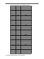
PCI-Interface Chip Registers
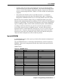
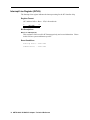
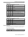
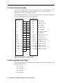
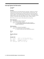
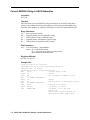
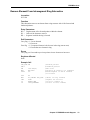
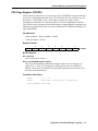
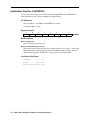
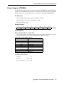
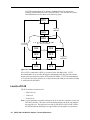
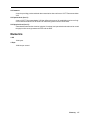
A diagram of the PCI Configuration Space Header is shown in the following figure.
The registers are described in detail following this diagram.
3&,((3520
ZULWHDEOH:ULWHDEOH
'HYLFH,'
9HQGRU,'
1<
3&,6WDWXV
3&,&RPPDQG
<1
5HY,'
&ODVV&RGH
+HDGHU
/DWHQF\
&DFKH/LQH
%,67
7\SH 7LPHU
6L]H
%DVH$GGUHVV5HJLVWHU
1<
1<
&<1
<1
%DVH$GGUHVV5HJLVWHU
<1
%DVH$GGUHVV5HJLVWHU
<1
%DVH$GGUHVV5HJLVWHU
&<1
%DVH$GGUHVV5HJLVWHU
<1
%DVH$GGUHVV5HJLVWHU
<1
5HVHUYHG V
6XEV\VWHP,'
0$;/$7
11
6XEV\VWHP9HQGRU,'
&1<
([SDQVLRQ520%DVH$GGUHVV
<1
5HVHUYHG V
11
5HVHUYHG V
,QWHUUXSW
0,1*17
3LQ
,QWHUUXSW
/LQH
Figure 2-1. PCI Configuration Space Header
18 ARTIC186 X.25 ISA/PCI Adapter: Technical Reference
11
&<<
&<<
PCI-Interface Chip Registers
Vendor Identification Register (VID)
The Vendor Identification register identifies the manufacturer of the PCI-interface chip.
This register is read-only from the PCI interface.
Register Format
(PCI Address Offset = Base + 00h–01h) 16-bit read-only
15
0
Vendor ID
Bit Descriptions
Bits 15–0: Vendor ID
This field identifies the manufacturer as IBM. Its value is 1014h. This register is
loaded by the Serial EEPROM at offset 40h.
Reset Conditions
Power-Up Reset - 0001 0000 1001 0100
Command Reset
- 0001 0000 0001 0100
Chapter 2: Programming Considerations 19
Device Identification Register (DID)
The Device Identification register identifies the particular device. This register is
read-only from the PCI interface.
Register Format
(PCI Address Offset = Base + 02h–03h) 16-bit read-only
15
0
Device ID
Bit Descriptions
Bits 15–0: Device ID
This read-only field identifies the device as an ARTIC186 X.25 ISA/PCI Adapter. Its
value is 0061. This register is loaded by the serial EEPROM at offset 42h.
Reset Conditions
Power-Up Reset - 0000 0000 0110 0001
Command Reset
- 0000 0000 0110 0001
20 ARTIC186 X.25 ISA/PCI Adapter: Technical Reference
PCI-Interface Chip Registers
PCI Command Register (PCICMD)
The PCI Command register provides the control of the PCI interface.
Register Format
(PCI Address Offset = Base + 04h–05h) 16-bit read/write
15
–
10
RESERVED
9
FBE
8
SDE
7
WCC
6
PER
5 – 3
RSVD
2
BME
1
MSE
0
IOSE
Bit Descriptions
Bits 15–10:
These bits are reserved and always read back as 0.
Bit 9: Fast Back-to-Back Enable
This function is not implemented on the co-processor adapter; this bit always reads 0.
Bit 8: -SERR Enable
This bit, when set, enables the co-processor adapter to drive -SERR on the system PCI
bus. This bit is reset to 0 with -SRST.
Bit 7: Wait Cycle Control
The co-processor adapter does not implement address/data stepping. This bit is
hardwired as 0 and always reads back as 0.
Bit 6: Parity Error Response
When is bit is set to 1, the co-processor adapter is enabled to check parity during
system PCI slave transactions. When reset to 0, parity errors are ignored.
Bits 5–3:
These bits are reserved and always read as 0.
Bit 2: Bus Master Enable
This function is not implemented on this adapter; this bit always reads as 0.
Bit 1: Memory Space Enable
When this bit is set to 1, the co-processor adapter is enabled to respond to PCI-bus
memory space accesses. This bit is reset to 0 during a PCI-bus RESET.
Bit 0: I/O Space Enable
When this bit is set to 1, the co-processor adapter is enabled to respond to PCI-bus I/O
space accesses. This bit is reset to 0 during PCI-bus RESET.
Reset Conditions
Power-Up Reset - 0000 0000 0000 0000
Command Reset
- 0000 0000 0000 0000
Chapter 2: Programming Considerations 21
PCI Status Register (PCISTS)
The PCI Status register provides the status of the PCI interface on the co-processor
adapter. Bits in the status field can be reset from 1 to 0 by writing a 1 to the corresponding
bit position.
Register Format
(PCI Address Offset = Base + 06h–07h) 16-bit read/write
15
DPE
14
SSE
13
RMA
12
RTA
11
STA
10 – 9
DEVSEL
8
DPR
7
FBC
6
–
0
RESERVED
Bit Descriptions
Bit 15: Detected Parity Error
This bit is set to 1 when the co-processor adapter detects a PCI-bus parity error,
regardless of the state of the Parity Error Response Bit in the Command Register
(PCICMD). A system configuration write of 1 to this bit sets it to 0.
Bit 14: Signaled System Error
This bit is set to 1 whenever the co-processor adapter asserts -SERR on the PCI bus. A
system configuration write of 1 to this bit sets it to 0.
Bit 13: Received Master Abort
This bit is set to 1 whenever the co-processor adapter receives a master abort signal.
This bit is reserved and always reads as 0.
Bit 12: Received Target Abort
This bit is reserved and always reads as 0.
Bit 11: Signaled Target Abort
This bit is set to 1 whenever the co-processor adapter signals a target abort. A system
configuration write of 1 to this bit sets it to 0.
Bits 10–9: Device Select Timing
This read-only field indicates the slowest device select timing of the co-processor
adapter on the PCI bus. Device select timing is set to 01b for medium timing.
Bit 8: Data Parity Reported
This function is not implemented on this adapter; this bit always reads as 0.
Bit 7: Fast Back-to-Back Capable
This bit is hardwired to 1, which indicates that the co-processor adapter can accept fast
back-to-back cycles as a target.
Bits 6–0:
These bits are reserved and always read as 0.
Reset Conditions
Power-Up Reset - 0000 0010 1000 0000
Command Reset
- 0000 0010 1000 0000
22 ARTIC186 X.25 ISA/PCI Adapter: Technical Reference
PCI-Interface Chip Registers
Revision Identification Register (RID)
The Revision Identification register contains the revision identification number.
Register Format
(PCI Address Offset = Base + 08h) 8-bit read-only
7
0
Revision ID
Bit Descriptions
Bits 7–0: Revision ID
This field specifies the silicon revision level of the ARTIC186 X.25 ISA/PCI Adapter.
This is a read-only function. This register is loaded by the Serial EPROM at offset 48h
Reset Conditions
Power-Up Reset - Current Revision
Command Reset
- Current Revision
Chapter 2: Programming Considerations 23
Class Code Register (CLCD)
The Class Code register defines the base class, sub-class, and programming interfaces for
the co-processor adapter.
Register Format
(PCI Address Offset = Base + 09h–0Bh) 24-bit read-only
24
0
Class Code
Bit Descriptions
Bits 23–0: Class Code
This field specifies the general function of the AMCC S5920Q PCI-interface chip.
This register is loaded by the Serial EEPROM at offset 49h. The value is 078000h,
representing:
Base Class = Simple Communication Controllers
SubClass = other communications device
Programming Interface = not defined.
Reset Conditions
Power-Up Reset - 0000 0111 1000 0000 0000 0000
Command Reset
- 0000 0111 1000 0000 0000 0000
24 ARTIC186 X.25 ISA/PCI Adapter: Technical Reference
PCI-Interface Chip Registers
Cache Line Size Register (CALN)
The Cache Line Size register is hardwired to 0. The co-processor adapter does not use the
PCI-bus commands Memory Write and Invalidate.
Register Format
(PCI Address Offset = Base + 0Ch) 8-bit read-only
7
0
Reserved
Bit Descriptions
Bits 7–0: Reserved
This field is reserved for setting the cache line size. This field reads back all zeroes.
Reset Conditions
Power-Up Reset - 0000 0000
Command Reset
- 0000 0000
Chapter 2: Programming Considerations 25
Latency Timer Register (LAT)
The Latency Timer register defines the number of PCI-bus clocks that the co-processor
adapter uses when it is a master.
Register Format
(PCI Address Offset = Base + 0Dh) 8-bit read-only
7
6
5 4 3 2
Reserved
1
0
Bit Descriptions
Bits 7–0:
These bits are reserved and always read as 0. These bits describe the latency timer
value. This function is not supported on the co-processor adapter.
Reset Conditions
Power-Up Reset - 0000 0000
Command Reset
- 0000 0000
26 ARTIC186 X.25 ISA/PCI Adapter: Technical Reference
PCI-Interface Chip Registers
Header Type Register (HDR)
The Header Type register describes the format of the device configuration header and
whether the co-processor adapter represents a single function or a multifunction PCI-bus
agent.
Register Format
(PCI Address Offset = Base + 0Eh) 8-bit read-only
7
SMF
6 5
4 3 2 1 0
Reserved
Bit Descriptions
Bit 7: Single/Multi Function
This bit defines whether the co-processor adapter represents a single-function
(bit 7 = 0) or a multi-function (bit 7 = 1) PCI-bus agent. Only an encoding value of 0 is
defined. Other values are reserved.
Bits 6–0: Reserved
These bits are reserved and always read as 0.
Reset Conditions
Power-Up Reset - 0000 0000
Command Reset
- 0000 0000
Chapter 2: Programming Considerations 27
Built-in Self-Test Register (BIST)
The Built-in Self-Test register permits the implementation of custom, user-specific
diagnostics.
Register Format
(PCI Address Offset = Base + 0Fh) 8-bit read-only
7 6
5
4 3 2
Reserved
1
0
Bit Descriptions
Bits 7–0: Reserved
These bits are reserved and always read as 0. This function is not supported on the coprocessor adapter.
Reset Conditions
Power-Up Reset - 0000 0000
Command Reset
- 0000 0000
28 ARTIC186 X.25 ISA/PCI Adapter: Technical Reference
PCI-Interface Chip Registers
Base Address Registers (BADR0 - 5)
The Base Address registers are used to assign memory or I/O accesses to the Local
Configuration registers and memory access to the Local Address Space for the coprocessor adapter. The actual location is determined by first interrogating these
registers to ascertain the size or space desired, then writing the high-order field of each
register to place it physically in the system address space. Base Address Register5 is
not implemented in the AMCC S5920Q chip.
Register Format
(BADR0 PCI Address Offset = Base + 10h) 32-bit read/write
(BADR1 PCI Address Offset = Base + 14h) 32-bit read/write
(BADR2 PCI Address Offset = Base + 18h) 32-bit read/write
(BADR3 PCI Address Offset = Base + 1Ch) 32-bit read/write
(BADR4 PCI Address Offset = Base + 20h) 32-bit read/write
(BADR5 PCI Address Offset = Base + 24h) 32-bit read/write
Base Address Register - Memory
31
–
30 29
–
4
AOBW
Base Address Location
3
PF
2− 1
LOC
0
SI
Base Address Register - I/O
−
Base Address Location
31
2
1
RSV
0
SI
Bit Descriptions
(Memory)
Bits 31–30: Add-On Bus Width
The decode of these two bits determines the bus size for each of the four add-on bus
regions. These bits apply only to BAR1–4.
D31
D30
Add On Bus Width
0
0
Region Disable
0
1
8 bits
1
0
16 bits
1
1
32 bits
Bits 29–4: Base Address Location
This read/write field specifies the starting PCI-bus address space for the ARTIC186
X.25 ISA/PCI Adapter memory space. Except for Base Address Register 0, these bits
are individually enabled by the contents sourced from the external boot memory.
Chapter 2: Programming Considerations 29
Bit 3: Prefetchable
A value of 1 indicates no side effect on reads.
Note: This bit is hardcoded to 0.
Bits 2–1: Location of Register
These two bits define whether the memory space is 32 or 64 bits wide and if the space
location is restricted to be within the first megabyte of memory space. The encoding is
as follows:
Bits
Description
2 1
0 0
Region is 32 bits wide and can be located anywhere in 32-bit memory space.
0 1
Region is 32 bits wide and must be mapped anywhere below the first MB of
memory space.
1 0
Region is 64 bits wide and can be mapped anywhere in 64-bit memory space.
(Not supported by this AMCC chip)
1 1
Reserved
Bit 0: Space Indicator
This bit is hardcoded to 0 to indicate a memory space definition.
(I/O)
Bits 31–2: Base Address Location
These bits are used to position the decoded region in I/O space.
Bits 31–2 are read/write.
Bit 1: Reserved
This bit is hardcoded to 0.
Bit 0: Space Indicator
This bit is hardcoded to 1 to indicate an I/O space definition.
Reset Conditions
Power Up Reset
BADR0 - 1111 1111 1111 1111 1111 1111 1000 0001
BADR1 - 0000 0000 0000 0000 0000 0000 0000 0000
BADR2 - 0000 0000 0000 0000 0000 0000 0000 0000
BADR3 - 0000 0000 0000 0000 0000 0000 0000 0000
BADR4 - 0000 0000 0000 0000 0000 0000 0000 0000
30 ARTIC186 X.25 ISA/PCI Adapter: Technical Reference
PCI-Interface Chip Registers
Subsystem Vendor Identification Register (SVID)
The Subsystem Vendor Identification register can provide a unique add-in board Vendor
ID. This register is read-only from the PCI interface. It can be written from the Serial
EEPROM.
Register Format
(PCI Address Offset = Base + 2Ch–2Dh) 16-bit read-only
15
0
Subsystem Vendor ID
Bit Descriptions
Bits 15–0: Subsystem Vendor ID
This read-only field uniquely identifies the user board or subsystem. It provides a
mechanism for add-in card vendors to distinguish with the same Vendor ID and Device
ID. This facility is not used on the co-processor adapter.
Reset Conditions
Power-Up Reset - 0000 0000 0000 0000
Boot-Load
- 1111 1111 1111 1111
Chapter 2: Programming Considerations 31
Subsystem Identification Register (SSID)
The Subsystem Identification register can provide a unique add-in board Device ID. This
register is read-only from the PCI interface.
Register Format
(PCI Address Offset = Base + 2Eh–2Fh) 16-bit read-only
15
0
Subsystem ID
Bit Descriptions
Bits 15–0: Subsystem ID
This register is not used on the co-processor adapter.
Reset Conditions
Power-Up Reset - 0000 0000 0000 0000
Boot-Load
- 1111 1111 1111 1111
32 ARTIC186 X.25 ISA/PCI Adapter: Technical Reference
PCI-Interface Chip Registers
Expansion ROM Base Address Register (XROM)
The Expansion ROM Base Address register is set to all zeros to disable the Expansion
ROM address of the co-processor adapter in PCI-bus address space.
Register Format
(PCI Address Offset = Base + 30h) 32-bit read-only
31
0
Reserved
Bit Descriptions
Bits 31–1:
These bits are reserved and always written as 0.
Reset Conditions
Power-Up Reset - 0000 0000 0000 0000 0000 0000 0000 0000
Command Reset
- SSSS SSSS SSSS SSSS SSSS S000 0000 000S
Chapter 2: Programming Considerations 33
Interrupt Line Register (INTLN)
The Interrupt Line register indicates the interrupt routing for the PCI-interface chip.
Register Format
(PCI Address Offset = Base + 3Ch) 8-bit read/write
7
0
INT LINE
Bit Descriptions
Bits 7–0: Interrupt Line
This read/write field is used for PCI interrupt priority and vector information. Values
in this field are system architecture specific.
Reset Conditions
Power-Up Reset - 0000 0000
Command Reset
- SSSS SSSS
34 ARTIC186 X.25 ISA/PCI Adapter: Technical Reference
PCI-Interface Chip Registers
Interrupt Pin Register (INTPIN)
The Interrupt Pin register identifies which PCI interrupt, if any, is connected to the
controller PCI-interrupt pins.
Register Format
(PCI Address Offset = Base + 3Dh) 8-bit read-only
7
0
INT PIN
Bit Descriptions
Bits 7–0: Interrupt Pin
This read-only field is read as X01 indicating connection to -INTA on the PCI bus.
This register is loaded from the serial EEPROM at offset 3Dh. The following values
are allowed:
00 = No Interrupt Pin
01 = -INTA
02 = -INTB
03 = -INTC
04 = -INTD
Reset Conditions
Power-Up Reset - 0000 0001
Command Reset
- 0000 0001
Chapter 2: Programming Considerations 35
Minimum Grant Register (MINGNT)
The Minimum Grant register can be optionally used by bus masters to specify how long a
burst period the device needs. This register is not supported in the AMCC S5920Q chip.
Register Format
(PCI Address Offset = Base + 3Eh) 8-bit read-only
7
0
MIN GRANT
Bit Descriptions
Bits 7–0: Minimum Grant
This read-only field is always read as zeros.
Reset Conditions
Power-Up Reset - 0000 0000
Command Reset
- 0000 0000
36 ARTIC186 X.25 ISA/PCI Adapter: Technical Reference
PCI-Interface Chip Registers
Maximum Latency Register (MAXLAT)
The Maximum Latency register can be optionally used by the bus masters to specify how
often the co-processor adapter needs PCI-bus access. A value of 00h indicates that the bus
master has no stringent requirement. This register is not supported in the AMCC S5920Q
chip.
Register Format
(PCI Config Offset = Base + 3Fh) 8-bit read-only
7
0
MAX LATENCY
Bit Descriptions
Bits 7–0: Maximum Latency
This read-only field is always read as zeros.
Reset Conditions
Power-Up Reset - 0000 0000
Command Reset
- 0000 0000
Chapter 2: Programming Considerations 37
AMCC S5920Q Add-On Pass-Thru Address and Data
Registers
Pass-Thru Address Register Summary
This register stores the address of any active Pass Thru PCI-bus cycle that has been
accepted by the AMCC S5920Q chip. The value contained in this register is always on a
doubleword boundary. The ARTIC186 X.25 ISA/PCI Adapter uses bits 2 through 13 of
this register (enough for the 8 KB memory window) to provide an address to the dual-port
memory controller to access the adapter DRAM. The MACH210 chip drives a signal
PTADR to the AMCC S5920Q chip to place the address for the current cycle on the
adapter DQ data pins. This address value is latched into the three 74ALS373 latch
modules. This step is necessary to demultiplex the address and data phases of the current
PCI-bus cycle.
Pass-Thru Data Register Summary
This register and the Pass-Thru Address register perform Pass-Thru transfers. When one
of the base address decode registers 1–4 encounters a PCI-bus cycle that selects the region
defined by it, the address register contains that current cycle’s active address and this data
register contains the data to be transferred to or from the PCI bus to the card Add-On bus.
The DQ pins of the AMCC S5920Q chip are connected directly to the dual-port memory
controller. The MACH210 module controls the gating and direction of data between the
PCI AMCC S5920Q chip and the dual-port memory controller. The address of this AddOn Data register (2C) is hardwired in logic; this is the only register needed to control the
transfer of data. All cycles between the PCI bus and the local Add-On bus are single data
phase transfers of 8 or 16 bits.
38 ARTIC186 X.25 ISA/PCI Adapter: Technical Reference
Dual-Port Memory Controller
Dual-Port Memory Controller
The dual-port memory controller provides a convenient and flexible way of passing data
and control bytes between the 80C186 bus and the system unit bus. This is accomplished
through an IBM CMOS gate array called the dual-port memory controller, which is an
array of 10000 gates. The chip adapts to both 8-bit and 16-bit data buses on the system
bus. The VLSI gate array’s basic purpose is to provide a high-performance interface
between the co-processor adapter and the system. All data communications between the
system and the co-processor adapter are through this interface. This is accomplished
through the following functions performed by the dual-port memory controller.
•
8 KB Page Selection from the System
The system unit can explicitly select any 8 KB page of RAM on the co-processor
adapter for writing or reading.
•
Interrupt Handling
The dual-port memory controller can generate interrupts to the system that are
initiated from the co-processor adapter. The dual-port memory controller also can
generate interrupts to the co-processor adapter that are initiated from the system.
•
RAM Contention
The dual-port memory controller interface is a dual-ported dynamic RAM controller
that arbitrates RAM accesses by both the system and the on-board 80C186 processor.
The arbitration occurs for read/write accesses and for dynamic RAM refresh by the
system.
•
Parity Error Handling
The co-processor adapter does not support parity memories. Therefore, the dual-port
memory controller does not generate nor check parity on the DRAM bus interface.
•
Watchdog Timer Errors
The dual-port memory controller detects watchdog timer expiration and interrupts
both the system and the co-processor adapter.
•
Initialization Conditions
The dual-port memory controller detects system resets and degates the on-board RAM
from the system bus to avoid corruption of RAM data. It also resets the co-processor
adapter after receiving an appropriate command from the system.
•
System Unit Lost Refresh Condition
The dual-port memory controller interrupts the co-processor adapter if the system
stops refreshing storage.
Chapter 2: Programming Considerations 39
Physical Characteristics
The co-processor adapter is designed for up to 1 MB of RAM storage. The system views
this memory space as 1288-KB pages. Only one page is selected by the system at any
given time. The page selector is a single-byte read/write I/O port register on the dual-port
memory controller. Accessing this register from either the system or the co-processor
adapter maps co-processor RAM storage for the system.
Performance
A 20 MHz clock (CLKIN) provides arbitration for the use of RAM. The dual-port
memory controller FPLD contains a simple DRAM arbiter that:
•
Gives the 80C186 interface the highest priority access to DRAM
•
Gives the next highest priority DRAM access to an internal refresh request
•
Gives lowest DRAM access priority to the ISA interface (non-refresh request).
All DRAM cycles occur in three CLKIN periods. The worst case contention to an
ISA-bus DRAM request is one 80C186 bus DRAM cycle (three CLKIN periods) plus an
internal refresh DRAM cycle (three CLKIN periods). (This is without the advantage of
the REFRESH# signal.) The number of ISA-bus wait states depends on the CLKIN
frequency and the operating mode of the ISA interface. DRAM accesses from the 80C186
bus normally run with zero wait states, but can result in one 80C186-bus wait state, worst
case, if a refresh or ISA-bus DRAM access has already started.
The dual-port memory controller is designed to provide maximum data throughput using a
minimum amount of software on the system. Very little synchronous operation is required
between the system and the co-processor adapter. This essentially asynchronous interface
allows system unit applications to communicate directly with applications on the coprocessor adapter through shared-storage space.
The dual-port memory controller has features that support maintenance and service. It
monitors a watchdog timer and, upon expiration, the dual-port memory controller
subsequently interrupts both the system and the 80C186 processor. Additionally, poweron diagnostics test basic functions and post error information to specific RAM locations.
During power-up sequences, the RAM storage is degated from the system to prevent the
system from attempting execution of the RAM-resident data that is mapped into the
system address space.
All control, data, and address lines from the system, co-processor adapter, and RAM enter
into the dual-port memory controller. Internally, the CPU signals are used to initiate
memory cycles to or from the RAM. After the processor is selected internally by the
arbitration unit, the appropriate RAM signals are generated and data is transferred (except
for a refresh, in which case there is no data involved). The arbitrator then de-selects the
processor that is using the RAM, and can then select another processor that is waiting to
use the RAM. Whenever the RAM is needed by both processors, one is selected and the
other is held in a wait state. A wait state for a processor is a variable integral number of
CPU clocks.
A major feature of the co-processor adapter is to relocate the memory and I/O space of the
co-processor adapter within the system memory and I/O space, through a value
programmed into internal registers of the dual-port memory controller. Because of the
40 ARTIC186 X.25 ISA/PCI Adapter: Technical Reference
Dual-Port Memory Controller
limited space within the system memory map, the co-processor adapter allows an 8 KB
window into the co-processor adapter RAM. The co-processor adapter and dual-port
memory controller support up to 1MB of RAM. To provide access to all data, the dualport memory controller contains a register that allows the user to change this window to
view different 8 KB portions of RAM. The co-processor adapter has access to all RAM
and has no need to use paging.
The dual-port memory controller has an internal refresh counter that refreshes all 1024
row addresses within 16 milliseconds (10x10 addressing) or all 4096 row addresses within
64 milliseconds (12x8 addressing). An external ISA-bus REFRESH# signal is not
required but, if supplied, the signal can improve ISA-bus performance by eliminating
ISA-bus contention with the asynchronous internal refresh counter. The REFRESH#
signal is sampled and, after it is detected active, it is synchronized to the internal refresh
cycle counter. If the REFRESH# signal is not detected active again within a 15.6
microsecond period, an internal refresh cycle occurs, which could cause wait states in an
ISA-bus DRAM access.
Programming Considerations
Within the dual-port memory controller several registers regulate the communication
between the co-processor adapter and the system. The following summarize the internal
registers and commands contained within the dual-port memory controller. Detailed
descriptions and bit definitions are in Appendix A: “Dual-Port Memory Controller” on
page 125.
Register and Command Descriptions
All registers are 8-bit read or read/write registers. However, because of the architecture
used in the system, 16-bit I/O writes can be used because the system unit translates them
into two 8-bit writes.
Note: When performing a 16-bit I/O write, the lower 8-bits are the even byte and the
upper 8-bits are the odd byte.
COMREG
Command Register. COMREG is used to issue commands to reset, interrupt, and
control the co-processor adapter.
CAD
Control Alt Delete Register. CAD0, CAD1, CAD2 registers are used to search for a
match of some specific address only accessed by the system after a Ctrl+Alt+Del,
which indicates a soft system reset to the co-processor. When the address match is
satisfied, the dual-port memory controller degates RAM.
CPUPG
CPU Page Register. CPUPG is used for page values by the system to access dynamic
RAM on the co-processor adapter. A page is 8 KB.
DREG
Data Register. DREG is a pseudo register used to access various registers pointed to by
the PTRREG.
Chapter 2: Programming Considerations 41
GAID
Gate Array Identification. GAID is used to identify which level of dual-port memory
controller is installed.
INITREG
Initialization Registers. INITREG0 and INITREG1 are used to configure the coprocessor dual-port memory controller, system interrupt level, I/O base address, and
type of system.
LOCREG
Location Registers. LOCREG0 and LOCREG1 are used to physically locate the coprocessor adapter memory space (8 KB) in the system memory map.
NMIMASK
Non-maskable Interrupt Mask Registers. NMIMASK is used to mask the various
sources of internal NMIs available.
NMISTAT
Non-maskable Interrupt Status Registers. NMISTAT is used to report which NMI is
active.
PTRREG
Pointer Register. PTRREG is used to point to and enable various other registers, which
then can be accessed through the pseudo register, DREG.
TREG
Task Register. TREG is used as a mailbox to pass data from the co-processor adapter
to the system. Writing to this register causes an interrupt to be generated to the system.
GEOI
Gate Array End of Interrupt Register. GEOI is used to clear the internal interrupt
circuitry of the dual-port memory controller after an interrupt is executed by the
system.
INITCOM
Interrupt Command Register. INITCOM is used to interrupt the co-processor.
ISEC
Interrupt Sharing Enable Command Register. ISEC is used to clear the internal
interrupt circuitry of the dual-port memory controller after an interrupt to the system.
Table 2-11. Register Addresses and Initial Values
Register
COMREG
Register
Description
CAD0 3
Command
Control Alt Delete 0
CAD1 3
Control Alt Delete 1
CAD2 3
Control Alt Delete 2
CPUPG
DREG
GAID
Data
Data
CPU Page
System Address Co-Processor
Adapter
Offsets (Hex)1,6 Address (Hex)
06
—
(0C)
—
(0D)
—
(0E)
—
05
14
03
—
0F
18
42 ARTIC186 X.25 ISA/PCI Adapter: Technical Reference
Power-Up
Value
(Binary) 2
0000 0000
0000 0000
0000 0000
0000 0000
UUUU UUUU
UUUU UUUU
0011 0000
Dual-Port Memory Controller
INITREG0 3
INITREG1
LOCREG0
LOCREG1
NMIMASK
NMISTAT
PTRREG
TREG
Initialization 0 4
Initialization 1
Location 0
Location 1
NMI Mask
NMI Status
Pointer
Task
(08)
04
0000 1000
—
00
01
—
—
02
04
06
00
02
08
0A
—
—
0000 0000
UUUU UUUU
UUUU UUUU
0011 1111
0000 0000
UUUU UUUU
1111 1111
Table 2-12. Command Addresses and Initial Values
Command Description
System Unit
Command
Address
(no data involved) 5
GEOI
Gate array end of cycle
Interrupt co-processor adapter
(09)
INTCOM 3
ISEC
ISEC
ISEC
ISEC
ISEC
ISEC
ISEC
ISEC
Interrupt sharing enable 3
Interrupt sharing enable 4
Interrupt sharing enable 7
Interrupt sharing enable 9, 2
Interrupt sharing enable A
Interrupt sharing enable B
Interrupt sharing enable C
Interrupt sharing enable F
Co-Processor
Adapter
16
02F3
02F4
02F7
02F2
06F2
06F3
06F4
06F7
Notes:
1. Values given in parentheses ( ) are pointer register values.
Values not in parentheses are offsets to the base I/O address defined by INITREG0.
2. 0 = Logic level 0; 1 = Logic level 1; U = Undefined.
3. Register is accessed using the pointer and data registers.
4. System unit can access only a portion of register.
5. Default power-up.
6. Values are not applicable.
Chapter 2: Programming Considerations 43
Other default power-up conditions include:
•
System unit side of co-processor adapter RAM is deactivated.
•
System unit side of co-processor adapter I/O is deactivated.
•
CAD feature is disabled.
•
Internal refresh counters and circuits are cleared.
•
Internal co-processor adapter interrupt circuits are cleared.
•
Internal system unit interrupt circuits are cleared.
Two initialization register bits in INITREG1 deserve special attention. Bit 0 and bit 1
represent edge connector (ED) jumper options and bus width (BW) respectively.
Note: These switches are disabled when the co-processor adapter is used as a PCI device.
In an 8088-based system unit, the ED bit should equal 1 and the BW bit should be 0.
Using an 8088-based system imposes the following restrictions:
•
The I/O bus is 8 bits wide.
•
Interrupt levels 10, 11, 12, and 15 are unavailable.
•
A maximum of 1 MB of system RAM/ROM space is available for locating (or
mapping) co-processor adapter memory.
Within an 80286-based system, multiple options are available through different settings of
ED and BW. The 80286 RAM/ROM memory region where a page of co-processor
adapter memory is mapped can be treated as either an 8-bit memory region or a 16-bit
memory region, and might be predefined by another adapter. Any one of the following
three conditions can exist:
•
The 80286 memory region is predefined as an 8-bit region.
The co-processor adapter is set up in the following way:
Set ED = 0, BW = 0, and LOCREG1 = 00h
•
The 80286 memory region is predefined as a 16-bit region.
The co-processor adapter can be set up in one of the following ways:
Set ED = 0 and BW = 1
or
Set ED = 0 and LOCREG1 > 00h
•
The 80286 memory region is undefined as either an 8-bit or a 16-bit region.
The co-processor is defining the region. Care must be exercised when operating
multiple devices in the same region.
Within an 80286-based system, the memory space can be divided into 128 sixteen-bit
regions, with each region being 128 KB wide and sometimes difficult to determine. The
first 512 KB of system RAM is four 16-bit regions. Having one edge connector defines
the adapter as an 8-bit device. The original monochrome adapter and color/graphics
adapter had only one edge connector. Therefore, A0000h to BFFFFh is an 8-bit region if
either of these adapters is installed.
44 ARTIC186 X.25 ISA/PCI Adapter: Technical Reference
Dual-Port Memory Controller
The region C0000h to DFFFFh has been predefined as an 8-bit region. The region
E0000h to FFFFFh is a 16-bit region. Other regions must be determined based on the
desired configuration. If the device uses the -MEMCS16 signal (pin D1 on the 36-pin
planar connector), the device is probably a 16-bit device.
Memory Mapping
Memory mapping is that process of translating a system unit memory access within the
window to the proper co-processor adapter location based partly on the system unit
address and the page register.
The dual-port memory controller provides this capability through use of the CPUPG,
LOCREG0, and LOCREG1 registers.
The system unit can view dynamic RAM storage on the co-processor adapter by mapping
a given 8 KB-page of RAM memory into an 8 KB page of its own address space
(normally, unused ROM space in the system unit is used).
This process is accomplished by:
•
Setting up the LOCREG0-1 to point to the desired 8 KB memory block boundary in
the system unit.
•
Setting up the CPUPG register to point to one of the 8 KB dynamic RAM pages.
Chapter 2: Programming Considerations 45
The following diagram illustrates the logical linkages required to map RAM page N into
the system memory block M. The system unit then can address the RAM space using its
own internal addressing.
Memory
Memory
High
8KB
Block 2047
High
8KB
Page 63
PROM space
Rom
Space
RAM 8KB
LOCREG0
page
(0-7Fh)
Block M
pointer
LOCREG1
(0-3Fh)
(0-7Fh)
1MB
RAM Page N
available
(128 pages max.)
Low
8KB
Block 0
Low
8KB
Page 0
Either the system unit or the 80C186 can select the active 8 KB-page of RAM by storing
the relative page number (0-3Fh) into the CPUPG register. Usually, the system unit
controls the active page except in the case of diagnostics or system restart initiated from
the 80C186. The page selector is a single-byte read/write I/O port on the system unit and
the co-processor adapter.
Either the system unit or the 80C186 can select the location at which the 8 KB-page of
RAM is mapped into the system unit storage space by storing the relative block number of
the system desired address location into the LOCREG 0 and 1 registers (0-7Fh and 0-Fh
respectively).
Accessing a page selector register (by either CPU) gates (connects, enables) the dynamic
RAM storage to the system unit.
46 ARTIC186 X.25 ISA/PCI Adapter: Technical Reference
Dual-Port Memory Controller
Address space on the co-processor adapter is represented by the following range.
8 KB Page Addresses
0–3Fh
0–7Fh
RAM Size
512 KB
1 MB
Accessing a non-RAM location due to the use of too large a page value can cause a parity
error.
Option Registers
Two option registers interface to the 80C186 bus. The registers provide buffers for
retention of option switch settings. The option switches specify interrupt levels, and bus
conventions. The address switch specifies the system unit I/O address.
Note: These switches are disabled when the co-processor adapter is used as a PCI device.
The registers, OPTION0 (at address 0080h) and OPTION1 (at address 0082h), can be read
at any time. The following diagrams show the option registers format and subsequent
discussion defines each bit.
Option 0
7
C7
Option 1
7
I/O Address = 00080h
6
C4
5
C2
4
C1
3
XX
2
L4
1
L2
0
L1
3
2
1
BW
0
ED
I/O Address = 00082h
6
5
4
Reserved
Chapter 2: Programming Considerations 47
Zilog Z8030 Serial Communications Controller
Functions
The primary function of the Z8030 serial communications controller (SCC) is to provide
control for the two independent serial communication channels. Each channel supports
communications through the X.25 network interface. Each channel has a transmitter and a
receiver and may be run in full-duplex or half-duplex mode.
After initial configuration of the SCC by the Realtime Control Microcode and applications
software, a major portion of the serial communications work load is taken from the
80C186 microprocessor and performed by the SCC.
The SCC provides:
•
Two independent full-duplex ports
•
Support for HDLC protocols
•
Automatic synchronization and address search for HDLC
•
Parity checking and generation
•
Break/abort detection and generation
•
Overrun and underrun detection
•
Internal signal wrapping
•
Interrupt vectoring
•
Full-duplex DMA operation
The SCC is a 44-pin plastic chip carrier package and is programmed to satisfy HDLC
protocol.
SCC Registers
Sixteen 8-bit registers for each port must be programmed before the SCC can be used.
Nine read registers (RR) for each port contain data and the status of the SCC. These are
RR0 through RR3, RR8, RR10, RR12, RR13 and RR15.
Fourteen write registers (WR) for each port are used for control. These are WR0, WR1,
WR3 through WR8, and WR10 through WR15.
Two registers, WR2 and WR9, are shared by both ports. They are set up by the RCM and
should not be modified by user tasks.
The base I/O address of the SCC is 100h.
48 ARTIC186 X.25 ISA/PCI Adapter: Technical Reference
Zilog Z8030 Serial Communications Controller
Write Registers
Table 2-13. SCC Write Register Addresses and Usage
Offset Offset
Register
Function
Port 0 Port 1
WR0
0020h 0000h Command register for configuring various modes
WR1
0022h 0002h Interrupt conditions to specify wait or DMA
WR2
0024h 0004h Interrupt vector. For adapter use only. If modified, results are
unpredictable.
WR3
0026h 0006h Receiver parameters. These are task controlled.
WR4
0028h 0008h Transmit/receive parameters
WR5
002Ah 000Ah Transmit parameters
WR6
002Ch 000Ch Sync character 1
WR7
002Eh 000Eh Sync character 2
WR8
0030h 0010h Transmit data buffer
WR9
0032h 0012h Master control/reset interrupt. For adapter use only. This
register should never be modified by a task.
WR10 0034h 0014h Miscellaneous transmit/receive control bits
WR11 0036h 0016h Clock mode control. Always set Bit 7 (no crystal) to zero
because no crystal is connected to the receiver clock input.
WR12 0038h 0018h Time constant low
WR13 003Ah 001Ah Time constant high
WR14 003Ch 001Ch Miscellaneous control bits. Bit 2 is transmit DMA request.
WR15 003Eh 001Eh External status control
Read Registers
Table 2-14. SCC Read Register Addresses and Usage
Offset Offset
Register
Function
Port 0 Port 1
RR0
0020h 0000h Transmit/receive and external status
RR1
0022h 0002h Special receive status
RR2
0024h 0004h Interrupt vector
RR3
0026h
Ports 0 and 1 Interrupt pending bits
RR8
0030h 0010h Receive data buffer
RR10
0034h 0014h Miscellaneous status and parameters
RR12
0038h 0018h Time constant low
RR13
003Ah 001Ah Time constant high
RR15
003Eh 001Eh External status control information
Programming the SCC
The PROM microcode provides several support subroutines to simplify programming the
SCC. Descriptions of these routines are in “PROM Microcode Support” on page 69.
Diagnostic Subroutine Support
Table 2-15. Diagnostic Subroutines
INT
Parms Function
FEh
AH=09h Reset an SCC port to default configuration.
Chapter 2: Programming Considerations 49
PROM Services
Table 2-16. PROM
INT
Parms
A2h
A4h
AAh
ACh
AEh
-
B0h
-
Services
Function
Reset an SCC port to the hardware default configuration.
General SCC register read/write
Assign the two 80C186 microprocessor DMA channels to two of the four
SCC DMA requests.
Configure and initialize DMA transfer types (I/O to memory and so on).
Read or write a 12-byte table to define DMA transfer source,
destination, and byte count.
Stop DMA transfer.
Programming Considerations
Consult the Zilog literature when programming the Z8030 SCC. The following are some
notes on programming the SCC on the adapter:
•
Although the Realtime Control Microcode initializes and manages the SCC, it is
possible to program the SCC directly to modify the default configuration.
Programming the SCC invalidates the control provided by the Realtime Control
Microcode which could affect the registers.
•
All functions and features of the SCC are not possible on the adapter. Some of the
write register bits must always be set to either 0 or 1 to support DMA and interrupts.
•
The SCC must operate in left-shift mode.
•
TRxCA must always be programmed as an input.
Zilog Z8036 Counter/Timer and Parallel I/O Unit
The Zilog Z8036 counter/timer and parallel I/O unit (CIO) is a fully programmable device
that provides peripheral I/O support and timer functions for hardware and software.
Functions
Some features of the Z8036 CIO are:
•
Two independent 8-bit, double-buffered, bidirectional I/O ports
•
4-bit special-purpose I/O port
•
Three independent 16-bit counter/timers with four external access lines per counter/
timer, programmable as retriggerable or non-retriggerable. The counter/timers can be
prescaled.
•
Interrupt vectoring
•
Pattern recognition
The adapter uses the CIO as follows:
•
Bi-directional ports 1 and 2 are available to application tasks running on the adapter.
•
The special purpose 4-bit port is used for diagnostics, the affected watchdog timer
I/O, and the electrical interface selection. It must not be used by application tasks.
50 ARTIC186 X.25 ISA/PCI Adapter: Technical Reference
Zilog Z8036 Counter/Timer and Parallel I/O Unit
•
Ports 0 and 1 are used in peripheral I/O control of data through the X.25 network
interface, and as control signals for data transfer to and from the SCC using DMA.
•
Timers 3 is the watchdog timer and must not be used by application tasks.
CIO Registers
The main CIO registers are dedicated for use by the RCM only and should not be directly
written to by applications. The base I/O address of the CIO is 0180h.
Bit definitions for each register are described in the Zilog Z8036 CIO Counter/Timer and
Parallel I/O Unit Technical Manual.
Table 2-17. CIO Main Control Registers
Offset
Access Function
0000h
R/W
Master interrupt control register
0002h
R/W
Master configuration control register
0004h
R/W
Port 0 interrupt vector
0006h
R/W
Port 1 interrupt vector
0008h
R/W
Counter/timer interrupt vector
000Ah
R/W
Port 2 data path polarity register
000Ch
R/W
Port 2 data direction register
000Eh
R/W
Port 2 special I/O control register
Table 2-18. Frequently Accessed Registers of the CIO
Offset
Access Function
0010h
R/W
Port 0 command and status
0012h
R/W
Port 1 command and status
0014h
R/W
Counter/timer 1 command and status
0016h
R/W
Counter/timer 2 command and status
0018h
R/W
Timer 3 command and status
001Ah
R/W
Port 0 data register
001Ch
R/W
Port 1 data register
001Eh
R/W
Port 2 data register
Table 2-19. CIO Counter/Timer Registers
Offset
Access
Function
0020h
R
Counter/timer 1 current count MSB
0022h
R
Counter/timer 1 current count LSB
0024h
R
Counter/timer 2 current count MSB
0026h
R
Counter/timer 2 current count LSB
0028h
R
Counter/timer 3 current count MSB
002Ah
R
Counter/timer 3 current count LSB
002Ch
R/W
Counter/timer 1 time constant MSB
002Eh
R/W
Counter/timer 1 time constant LSB
0030h
R/W
Counter/timer 2 time constant MSB
0032h
R/W
Counter/timer 2 time constant LSB
0034h
R/W
Counter/timer 3 time constant MSB
0036h
R/W
Counter/timer 3 time constant LSB
0038h
R/W
Counter/timer 1 mode specification
003Ah
R/W
Counter/timer 2 mode specification
003Ch
R/W
Counter/timer 3 mode specification
003Eh
R/W
Current vector
Chapter 2: Programming Considerations 51
Table 2-20. CIO Port 0 Specification Registers
Offset
Access Function
00040h
R/W
Port 0 mode specification. Bits 3–7 must be zeros to keep the port
specified as a bit port. The deskew timer function is not supported.
Bit 0 is latched on pattern match.
00042h
R/W
Port 0 handshake specification. (This register is always zero because
handshaking is not used.)
00044h
R/W
Port 0 data path polarity
00046h
R/W
Port 0 data direction
00048h
R/W
Port 0 special I/O control
0004Ah
R/W
Port 0 pattern polarity
0004Ch
R/W
Port 0 pattern transition
0004Eh
R/W
Port 0 pattern mask (which bits to test)
Table 2-21. CIO Port
Offset
Access
00050h
R/W
00052h
R/W
00054h
R/W
00056h
R/W
00058h
R/W
0005Ah
R/W
0005Ch
R/W
0005Eh
R/W
0 Specification Register
Function
Port 1 mode specification.
Port 1 handshake specification
Port 1 data path polarity
Port 1 data direction
Port 1 special I/O control
Port 1 pattern polarity
Port 1 pattern transition
Port 1 pattern mask
Programming the CIO
The PROM microcode provides several support subroutines to simplify programming the
CIO. See Chapter 5. “PROM Microcode Support” on page 69 for subroutine descriptions.
Diagnostic Subroutines
Table 2-22. Diagnostic Subroutines
INT
Parameter Function
FEh
AH=08h
Initialize a CIO port.
FEh
AH=0Bh
Initialize a CIO timer.
PROM Services
Table 2-23. PROM Services
Parameter
Parameter Function
A6h
Read/write CIO port registers
A8h
Timer1 and timer2 control
Programming Considerations
The Zilog literature should be consulted when programming the Z8036 CIO. The
following are some notes on programming the CIO on the adapter:
•
The Z8036 operates in left-shift mode.
•
I/O operations to the CIO must be separated by a least one microprocessor instruction
because the 80C186 microprocessor can process I/O operations faster than the CIO
can handle them.
52 ARTIC186 X.25 ISA/PCI Adapter: Technical Reference
Zilog Z8036 Counter/Timer and Parallel I/O Unit
•
The CIO counter/timers are treated as separate devices from the CIO ports to allow
flexibility in assigning timer resources to tasks.
•
The timers are driven by 3.6864 MHz clock.
CIO Port Assignments and Description
One port and one timer of the CIO are used by the watchdog timer to provide interrupt
notification of a runaway CPU. The remaining ports of the CIO are used for the
interfaces. Port 0 is used for the X.21 bis/V.24 Interface and the X.21 bis/V.35. Port 1 is
used for the X.21 Interface, and port 2 is used for the selection of V.24 or V.35 Interface
and the watchdog timer. The following tables show the bit assignments for the CIO.
Table 2-24. CIO Bit Assignments, Port 0
Port 0
Pin No.
Signal
P0-0
37
DSR
P0-1
36
Unused
P0-2
35
LLBT
P0-3
34
RLBT
P0-4
33
CI
P0-5
32
TI
P0-6
31
DTR
P0-7
30
Unused
Description
Data set ready
Local loopback test
Remote loopback test
Call indicate
Test indicate
Data terminal ready
-
Table 2-25. CIO Bit Assignments, Port 1
Port 1
Pin No.
Signal
Description
P1-0
10
IND
Indicate
P1-1
11
CABLE-0
Cable ID 0
P1-2
12
CABLE-1
Cable ID 1
P1-3
13
RXD 1
Receive data
P1-4
14
SYNC 1
Transmit clock 1
P1-5
15
RXTXC 1
Receive clock 1
P1-6
16
CTRL 1
Control
P1-7
17
X.21 Tx
X.21 transmit enable
The bit assignments for port 2 are shown in the following watchdog timer section.
Watchdog Timer
The watchdog timer detects runaway tasks. Once activated, the timer must be continually
monitored by software to prevent it timing out. If a task running on the adapter has an
unrecoverable error, the watchdog timer times out, and the CIO does the following:
•
Activates a light-emitting diode (LED) on the adapter.
Sends a nonmaskable interrupt (NMI) to the 80C186 microprocessor (if not masked in the
NMIMASK register in the dual-port memory controller).
•
Sends an interrupt to the system unit by loading FEh into the task register (TREG) in
the dual-port memory controller (if not masked).
Chapter 2: Programming Considerations 53
Table 2-26. LED Operation
P2-2
P2-0
0
0
0
1
1
0
1
1
LED
On
On
Off
On
The range of the watchdog timer is from 1.1 milliseconds to 72.81659 seconds with a step
size of 1.1 milliseconds.
Timer 3 in the CIO is used as the watchdog timer. If the watchdog timer is never
initialized, the LED remains lit.
Table 2-27. Watchdog Timer Description
Port 2
Pin No.
Signal
Description
(See Note)
P2-0
19
WDOG
Timer 3 out, watchdog
P2-1
20
T3CLK
Timer 3 clock input 900 Hz.
P2-2
21
WD CNTL
Watchdog LED control.
P2-3
22
V.24/V.35
Selection of V.24 or V.35 interface
Note: Port 2 on the CIO can be programmed by the user.
54 ARTIC186 X.25 ISA/PCI Adapter: Technical Reference
Chapter
3
3
External Interface
This chapter describes the external interfaces of the ARTIC186 X.25 ISA/PCI Adapter
Co-Processor.
General Connections
The general connection of the ARTIC186 X.25 ISA/PCI Adapter Co-Processor to an X.25
public packet-switched network is shown in the following figure.
D-37
X.25 Adapter
X.21 and
X.21 bis
Logic
DCE
X.25
network
Cable and Connectors
Figure 3-1. Connecting the Adapter to an X.25 Public Packet-Switched Network
Three network interfaces are available on a common 37-pin D-type male connector on the
adapter:
•
X.21
•
X.21 bis/V.24 (EIA-232)
•
X.21 bis/V.35
Note: If the HRS signal is required on the EIA-232 interface, then another cable is
required. X.21 bis/V.24 uses the LLBT signal instead of the HRS.
Each interface fully conforms to the CCITT Recommendation X.25 (1984), and to ETSI
Standards.
•
NET 1 - Approval requirements for data terminal equipment to connect to circuit
switched public data networks and leased circuits using CCITT Recommendation
X.21 interface
•
NET 2 - Approval requirements for data terminal equipment to connect to packet
switched public data networks using CCITT Recommendation X.25 interface
Three cables are available, each connecting one interface to the data circuit-terminating
equipment (DCE) of a packet-switched network. Each cable has a D-37 female connector
at the adapter end and one of the following at the DCE end:
Chapter 3: External Interface 55
•
D-15 male connector (for X.21)
•
D-25 male connector (for X.21 bis/V.24)
•
M/34 block male connector (for X.21 bis/V.35)
Using the cables supplied, only one interface can be connected to a DCE at any time.
Two pins on the adapter end of the cables uniquely identify the type of cable as shown in
“Cable Identification” on page 60.
56 ARTIC186 X.25 ISA/PCI Adapter: Technical Reference
General Connections
X.21 Interface
The X.21 interface consists of synchronous full-duplex, balanced, double-current
interchange, digital circuits that can operate at signaling rates of up to 64 kbps. The
interface fully conforms to CCITT Recommendation X.27 (equivalent to recommendation
V.11). The interface cable conforms to ISO 4903 at the D-15 connector end. The X.27
recommendation is electrically compatible with EIA RS-422-A. Figure 3-2 shows the
X.21 interface control detail.
The data path for the X.21 interface is provided by port 1 of the SCC. The control signals
for the interface are provided by port 1 of the CIO. An X.21 transmit-enable signal (X21TX-EN) is derived from P1-7 of the CIO. This signal must be set to logical 1 before
transmission of data.
The type of interface cable connected can be identified by reading pins 9 and 15 of the
D-37 connector (ID0 and ID1). The identifier for an X.21 interface cable is ID0=0,
ID1=1. See Table 3-1 on page 60 for the identifiers of the other types of cable.
' & R QQ H F W R U
=6&&
7['
5['
75[&
5 7 6 %
& 7 6 %
'&'%
57[&
;
(OHFWULFDO
,QWHUIDFH
$VVHPEO\
6<1&
=&,2
3
3
3
3
3
3
*1'
7$
7%
5$
5%
6*
,$
,%
6$
6%
&$
&%
;7;(1
9
3
3
,'
,'
Figure 3-2. X.21 Interface Control
Chapter 3: External Interface 57
X.21 bis/V.24 Interface (EIA-232)
The X.21 bis/V.24 interface consists of unbalanced, double-current interchange circuits
that can operate at signaling rates from 2400 to 19200 bits per second. The interface fully
conforms to CCITT Recommendation V.28, which is electrically identical to EIA
RS-232C. The interface cable conforms to ISO 2110 at the D-25 connector end.
Figure 3-3 shows the X.21 bis/V.24 interface control.
The data path for the X.21 bis/V.24 interface is provided by port 0 of the SCC. The
control signals for the interface are provided by port 0 of the CIO. A select signal, V24
(not V35) is derived from P2-3 of the CIO. This signal must be set to logical 1 before
transmission of data. RTS (pin 4) must be set to logical 1 to enable transmission of data at
pin 2.
The type of interface cable connected can be identified by reading pins 9 and 15 of the D37 connector (ID0 and ID1). The identifier for an X.21 bis/V.24 interface cable is ID0=0,
ID1=0. See Table 3-1 on page 60 for the identifiers of the other types of cable. At power
up, if the cable is installed, the PROM code reads the cable ID and sets the select signal
appropriately.
=6&&
7;'$
576$
5;'$
&76$
'&'$
75[&$
57[&$
6<1&$
;
(OHFWULFDO
,QWHUIDFH
$VVHPEO\
=&,2
3&
'&RQQHFWRU
7;'
576
5;'
&76
&'
9B5[B&/.
9B7[B&/.
*1'
99
3$ 3$
3$ 3$
3$ 3$
6*
//%7
'57
'65
)/%7
&,
7,
9
3%
3%
Figure 3-3. X.21 bis/V.24 Interface Control
58 ARTIC186 X.25 ISA/PCI Adapter: Technical Reference
,'
,'
General Connections
X.21 bis/V.35 Interface
The X.21 bis/V.35 interface consists of balanced and unbalanced, double-current,
interchange circuits that can operate at signaling rates of up to 56000 bits-per-second.
Data and timing signals are carried by balanced circuits, which fully conform to CCITT
Recommendation V.35. The unbalanced circuits are used for control signals and fully
conform to CCITT Recommendation V.28, which is electrically identical to EIA RS232C. The interface cable conforms to ISO 2593 at the M/34 block connector. Figure 3-4
shows the X.21 bis/V.35 interface control.
The data path for the X.21 bis/V.35 interface is provided by port 0 of the SCC. The
control signals for the interface are provided by port 0 of the CIO. A select signal V24
(not V35) is derived from P2-3 of the CIO. This signal must be set to logical 0 prior to
data transmission. RTS (pin 4) must be set to logical 1 to enable data transmission at pins
35 and 17.
The type of interface cable connected can be identified by reading pins 9 and 15 of the D37 connector (ID0 and ID1). The identifier for an X.21 bis/V.35 interface cable is ID0=1,
ID1=0. See Table 3-1 on page 60 for the identifiers of the other types of cable. At power
up, if the cable is installed, the PROM code reads the cable ID and sets the select signal
appropriately.
'
&RQQHFWRU
=6&&
7;'2
5762
5;'2
&762
'&'2
75[&2
57[&2
6<1&2
;
(OHFWULFDO
,QWHUIDFH
$VVHPEO\
=&,2
32
32
32
32
*1'
576
7;'$
7;'%
&76
5;'$
5;'%
5;&/.$
5;&/.%
7;&/.$
7;&/.%
&'
6*
'57
'75
'65
&,
99
'65
&,
9
3
3
,'
,'
Figure 3-4. X.21 bis/V.35 Interface Control
Chapter 3: External Interface 59
Cables and Connectors
A D-37 wrap plug is available for the adapter and each type of cable is supplied with a
wrap plug for the connector at the DCE end.
Cable Identification
Two pins on the D-37 connector are used as cable identifiers. Pull-up resistors on the
adapter hold these pins at +5 volts unless they are pulled to ground by connections in the
D-37 female connector, as shown in the following figure.
8036 ID 0
C IO
ID 1
.
Figure 3-5. Cable ID (X.21 bis/V.24 Interface Cable Connected)
The following table shows the identifier for the X.21, X.21 bis/V.24, and X.21 bis/V.35
interface cables, and for the D-37 wrap plug.
Table 3-1. Cable and Wrap Plug Identification
Cable
ID0
ID1
X.21 bis/V.24
0
0
X.21
0
1
X.21 bis/V.35
1
0
D-37 Wrap
1
1
To test for the presence of a D-37 wrap plug:
1
Look for logical 1 on both ID0 and ID1.
2
Reprogram ID0 (P1-1 of the CIO) as an output.
3
Write logical 0 to P1-1.
4
Read ID1.
If ID1 is logical 0, a wrap plug is connected; otherwise no plug is connected.
60 ARTIC186 X.25 ISA/PCI Adapter: Technical Reference
Cables and Connectors
D-37 Connector
The connections to the D-37 connector for all three interfaces are shown in the following figure. A wrap
plug is supplied to loopback transmitted signals at the D-37 connector. See “D-37 Wrap Plug” on page 65
for more information.
3LQ
6LJQDO1DPH
5HVHUYHG
7UDQVPLWWHG'DWD
5HFHLYHG'DWD
5HTXHVWWRVHQG
&OHDUWRVHQG
'DWDVHWUHDG\
6LJQDOJURXQG
&DUULHUGHWHFW
&DEOH,'$
7UDQVPLWWHGGDWD$
&RQWURO$
5HFHLYHGGDWD$
,QGLFDWLRQ$
7UDQVPLWFORFN$
&DEOH,'
5HFHLYHFORFN%
7UDQVPLWWHGGDWD%
7UDQVPLWFORFN%
5HFHLYHGGDWD%
'DWDWHUPLQDOUHDG\
5HPRWHORRSEDFNWHVW
&DOOLQGLFDWH
5HVHUYHG
7UDQVPLWFORFN
7HVWLQGLFDWH
5HFHLYHFORFN
/RFDOORRSEDFNWHVW
7UDQVPLWWHGGDWD%
&RQWURO%
5HFHLYHGGDWD%
,QGLFDWLRQ%
7UDQVPLWFORFN%
5HVHUYHG
5HFHLYHFORFN$
7UDQVPLWWHGGDWD$
7UDQVPLWFORFN$
5HFHLYHGGDWD$
$EEUHYLDWLRQ
7;'
5;'
576
&76
'65
*1'
&'
,'$
7$
&$
5$
,$
6$
,'%
5;&/.%
7;'%
7;&/.%
5;'%
'75
5/%7
&,
7;&/.
7,
5;&/.
//%7
7%
&%
5%
,%
6%
5;&/.$
7;'$
7;&/.$
5;'$
Figure 3-6. X.25 Network Interface Connector
Chapter 3: External Interface 61
X.21 Interface Cable
The X.21 interface cable is 3 meters long. It has a D-37 female connector at the adapter
end and a D-15 male connector at the DCE end. The cable conforms to the Underwriters’
Laboratory Specification UL 2943.
The following figure shows the X.21 interface cable. A wrap plug is supplied to perform
local loopback tests at the D-15 connector.
'&RQQHFWRU
'&RQQHFWRU
7$
7$
&$
&$
5$
5$
,$
,$
6$
6$
*1'
*1'
7%
7%
&%
&%
5%
5%
,%
,%
6%
6%
,'
Figure 3-7. X.21 Interface Cable
62 ARTIC186 X.25 ISA/PCI Adapter: Technical Reference
Cables and Connectors
X.21 bis/V.24 Interface Cable
The X.21 bis/V.24 interface cable is 3 meters long. It has a D-37 female connector on the
adapter end and a D-25 male connector at the DCE end. The cable conforms to
Underwriters’ Laboratory Specification UL 2464.
The X.21 bis/V.24 interface cable is shown in the following figure. A wrap plug is
supplied to perform local loopback tests at the D-25 connector.
'&RQQHFWRU
'&RQQHFWRU
7;'
7;'
5;'
5;'
576
576
&76
&76
'65
'65
*1'
*1'
&'
&'
7;&/.
7;&/.
5;&/.
5;&/.
//%7
//%7
'75
'75
5/%7
5/%7
&,
&,
7,
7,
,'
,'
Figure 3-8. X.21 Bis/V.24 Interface Cable
Chapter 3: External Interface 63
X.21 bis/V.35 Interface Cable
The X.21 bis/V.35 interface cable is 3 meters long. It has a D-37 female connector at the
adapter end and a M/34 block connector at the DCE end. The cable conforms to
Underwriters’ Laboratory Specification UL 2493.
The following figure shows the X.21 bis/V.35 interface cable. A wrap plug is supplied to
perform local loopback tests at the M/34 connector.
'&RQQHFWRU
0&RQQHFWRU
*1'
%*1'
6LJQDOJURXQG
576
&576
5HTXHVWWRVHQG
&76
'&76
&OHDUWRVHQG
'65
('65
'DWDVHWUHDG\
&'
)&'
&DUULHUGHWHFW
'75
+'75
'DWDWHUPLQDOUHDG\
&,
-&,
&DOOLQGLFDWH
7;'$
37;'$
7UDQVPLWWHGGDWD$
5;'$
55;'$
5HFHLYHGGDWD$
7;'%
67;'%
7UDQVPLWWHGGDWD%
5;'%
75;'%
5HFHLYHGGDWD%
5;&/.$
95;&/.$ 5HFHLYHFORFN$
7;&/.$
<7;&/.$ 7UDQVPLWFORFN$
5;&/.%
;5;&/.% 5HFHLYHFORFN%
7;&/.%
$$7;&/.% 7UDQVPLWFORFN%
,'
Figure 3-9. X.21 Bis/V.35 Interface Cable
Local Loopback-Test Plugs
The following wrap plugs are supplied for local loopback tests in accordance with CCITT
Recommendation X.150:
•
D-37 wrap plug
•
D-15 wrap plug
•
D-25 wrap plug
•
M/34 wrap plug
64 ARTIC186 X.25 ISA/PCI Adapter: Technical Reference
Local Loopback-Test Plugs
D-37 Wrap Plug
The D-37 wrap plug is used to test local loopback at the D-37 connector on the adapter. It
has a cable identifier of ID0=1, ID1=1. See “Cable Identification” on page 60 for a
method of distinguishing between an open circuit and the presence of a D-37 wrap plug.
The pin assignment of the D-37 wrap plug is shown in the following figure.
6LJQDO3LQ1R3LQ1R6LJQDO
7%5%;
7$5$
&%,%
&$,$
7;'5;';ELV9
576&76
'75'65
//%77,
5/%7&,
7;'$5;'$;ELV9
7;'%5;'%
7;&/.709
5;&/.%7;&/.%9;
7;&/.$5;&/.$9;
,','&DEOH,'
Figure 3-10. D-37 Wrap Plug Pin Assignment
D-15 Wrap Plug
The D-15 wrap plug is used to test loopback at the DCE end of the X.21 interface cable.
The pin assignment of the D-15 wrap plug is shown in the following figure.
6LJQDO3LQ1R3LQ1R6LJQDO
7%5%
7$5$
&%,%
&$,$
Figure 3-11. D-15 Wrap Plug Pin Assignment
Chapter 3: External Interface 65
D-25 Wrap Plug
The D-25 wrap plug is used to test loopback at the DCE end of the X.21 bis/V.24 interface
cable. The pin assignment of the D-25 wrap plug is shown in the following figure.
6LJQDO3LQ1R3LQ1R6LJQDO
7;'5;'
576&76
'75'65
//%77,
5/%7&,
Figure 3-12. D-25 Wrap Plug Pin Assignment
M/34 Wrap Plug
The M/34 wrap plug is used to test loopback at the DCE end of the X.21 bis/V.35 interface
cable. The pin assignment of the M/34 wrap plug is shown in the following figure.
6LJQDO3LQ1R3LQ1R6LJQDO
7;'$355;'$
7;'%675;'%
576&'&76
'75+('65
Figure 3-13. M/34 Wrap Plug Pin Assignment
66 ARTIC186 X.25 ISA/PCI Adapter: Technical Reference
Chapter
4
4
Adapter Characteristics
This chapter describes the physical and electrical characteristics of the ARTIC186 X.25
ISA/PCI Adapter hardware.
Physical Characteristics
Adapter Size
The dimensions of the adapter and the positions of the D-37 connector are shown in the
following figure.
4.1875 in.
6.875 in.
Figure 4-1. ARTIC186 X.25 ISA/PCI Adapter
Adapter Technology
The adapter consists of the following:
•
Two power planes (+5 V, 0 V)
•
Six signal planes
•
Vias where required
•
Predominantly surface-mounted components
•
Some pin-in-hole components
Adapter Connectors
The adapter has three I/O connectors:
•
PCI bus connector. This is a 124-pin edge connector that lets the adapter be plugged
into any 5.0 Volt PCI-compliant slot of the system unit.
Chapter 4: Adapter Characteristics 67
•
ISA bus connector. This is a 98-pin edge connector that lets the adapter be plugged
into any 16-bit ISA-compliant slot of the system unit.
•
37-pin D-type (D-37) connector. This is the electrical interface from the adapter to the
data network. It must be connected to one of the specific electrical interfaces
supported, using a cable with an appropriate socket. See Chapter 3 "External
Interface" on page 55 for more information.
Electrical Characteristics
Table 4-1. Power Requirements
Supply voltage
Current (maximum)
+4.8 V dc to +5.25 V dc
0.95 A
+11.3 V dc to +12.7 V dc
10 mA
-11.3 V dc to -12.7 V dc
16 mA
Environmental Characteristics
Table 4-2. Environmental Classification Ratings
Standard Classification
Rating
Acoustic
Class 2
Environmental
Class E
G1
P1
Vibration and shock
V2/S2
EMI limit (FCC rules)
Class A
CISPR
Class A
Thermal
Air Temperature
Operating: 1 to 52 degrees C
Storage: 1 to 60 degrees C
Shipping -40 to 60 degrees C
Humidity
Operating: 5% through 95%.
Cooling
The adapter is cooled by the existing airflow provided by the system unit. There are no
additional cooling requirements.
Heat Output
The heat output of the adapter is 5.1 watts, based on maximum current consumption.
Usability Characteristics
The usability of the adapter with regard to communication and data transfer is dependent
on the communication application software running on the adapter and the overall
usability of the system unit in which the adapter is installed.
68 ARTIC186 X.25 ISA/PCI Adapter: Technical Reference
Chapter
5
PROM Microcode Support
5
This chapter describes the details of PROM microcode support for the ARTIC186 X.25
ISA/PCI Adapter.
Support Provided
The PROM microcode provides support for:
•
Power-on self-test (POST)
•
Diagnostic subroutines
•
PROM services
•
Dump routines
•
Bootstrap loader.
Power-On Self-Test
When the system unit is powered on, the PROM microcode performs the following steps:
1. Clears the PROM-ready bit in the dual-port memory controller
2. Tests the 80186 microprocessor flags and conditional jumps
3. Tests the 80186 microprocessor registers
4. Tests the 80186 microprocessor chip-select registers and sets their default values
5. Tests low DRAM (approximately the lowest 1.3 KB used by the PROM microcode)
and sets the adapter primary status byte (PSB) to busy (C0h)
6. Tests stack operation and CALL/RETURN instructions
Note: A failure at step 2, 3, 4, or 6 is unrecoverable. A failure at
step 5 can be recoverable or unrecoverable.
7. Determines the size of installed DRAM and stores the value in TSIZE in the PROM
work area
8. Puts C9C9h in DBIDS in PROM work area
9. Puts ABBAh in ABBA and puts the adapter I/O address in IOADR in the PROM work
area
10. Sets hardware configuration descriptor (HCD) to 0
Chapter 5: PROM Microcode Support 69
11. Begins power-on self-test (POST) by doing the following:
a. Sets up the entire vector area
b. Checks that any errors in the PROM microcode DRAM test were recoverable
c. Calls the Test Processor Diagnostic subroutine (to test 80186 microprocessor
timers, DMA channels and interrupts)
d. Calls the Test Dual-Port Memory Controller diagnostic subroutine (to test dualport memory controller registers)
e. Tests DMA allocation register
f.
Calls the Checksum Memory Diagnostic subroutine (to checksum PROM)
g. Calls the Test DRAM Diagnostic subroutine (to test DRAM not already tested)
h. Tests the operation of the DRAM parity circuit
i.
Calls the Test CIO Diagnostic subroutine (to test basic functions of the CIO)
j.
Calls the Test SCC Diagnostic subroutine (to test basic functions of the SCC)
k. Turns off the error LED if no errors were detected
Note: POST terminates immediately when it detects an error, the remaining tests
of POST are not run, and the error LED remains lit.
l.
Initializes CIO, SCC, 80186 microprocessor, DMA, and timers
m. Puts default values in interface block (PSB=C0h)
n. Puts size of installed DRAM in TSIZE, puts C9C9h in DBIDS, and HCD in
interface block
o. Puts extended interface ID in TEMP_IDX in PROM work area
p. Puts any POST error data in secondary status area of interface block
q. Sets PSB to 00h (no errors, not busy) or 30h (recoverable error)
r.
Sets PROM Ready bit.
Errors
Errors are classed as either unrecoverable or recoverable.
For the POST tests, the primary status area starts at memory location 000414h. The
secondary status area starts at memory location 00047Dh.
Unrecoverable Errors
When the PROM microcode detects an unrecoverable error, it immediately terminates the
test, disables I/O, and lights the error LED. A failure at any of steps 2, 3, 4, or 6 is
unrecoverable.
A failure at step 5 can be unrecoverable or recoverable. The low DRAM test is run four
times and the number of failed attempts noted. If all four attempts fail, the error is
considered to be unrecoverable. The PROM microcode disables I/O and flashes the error
LED rapidly to identify this particular error.
70 ARTIC186 X.25 ISA/PCI Adapter: Technical Reference
Power-On Self-Test
If less than four attempts failed, the error is considered to be recoverable.
Recoverable Errors
When the first recoverable error is detected, POST terminates, and the PROM microcode
executes steps 11.l through 11.r to set up the normal hardware and software environment.
Details of the error are logged in a 7-byte table in the secondary status area in the format
shown in the following table.
No Errors
If no errors were detected in tests 11.a through 11.r, the PROM microcode sets the primary
and secondary status blocks to all zeros and turns off the error LED.
Table 5-1. POST Error Codes
Test
80186 microprocessor internal devices
DRAM
PROM checksum
CIO
SCC
Dual-Port Memory Controller
Parity circuits
DMA allocation register
0
1
01
01
01
01
01
01
01
01
01
02
03
04
05
06
07
08
2–3
Offset
-
4–5
Segment
-
6
Data
-
Byte 0 indicates an error during POST. Byte 1 indicates the device that failed.
Bytes 2 through 5 give the location of DRAM failure. If the low DRAM test failed this is
the location of the last failure. Byte 6 contains the incorrect bit mask (error bits are 1).
Table 5-2. POST Error Codes
POST Error
No Error Detected
NO ERROR DETECTED
Catastrophic Errors
PROC INDIC/COND JUMPS
PROC 1ST REG TEST
MCS REG FAILURE
JUMPERS WRONG - M2,M1 = 11
CALL INSTR OR STACK FAILURE
VECTOR AREA RAMTEST FAILURE
80186 Internal Devices
PERIPHERAL REGISTER FAILURE
CPU TIMER FAILURE
DMA FAILURE
INTERRUPT TEST FAILURE
RAM Test
LOW RAM TEST FAILURE
LOW RAM TEST FAILURE
LOW RAM TEST FAILURE
LOW RAM TEST FAILURE
HIGH RAM TEST FAILURE
PROM Checksum
PROM CHECKSUM
Primary Status
Secondary Status
0000
-- --
**
**
**
**
**
**
** **
** **
** **
** **
** **
** **
0101
0102
0103
0104
01 01
01 01
01 01
01 01
0201
0202
0203
0204
0205
01 02 ***
01 02 ***
01 02 ***
01 02 ***
01 02 ***
0301
01 03
Chapter 5: PROM Microcode Support 71
Table 5-2. POST Error Codes (Continued)
POST Error
Primary Status
CIO 0 Test
CIO REG FAILURE
0401
0402
TMR ERR INT OCCURRED
0403
TMR2 - NO INTERRUPT
TMR2 CNT LSB NZ AT INTRPT
0404
TMR2 CNT MSB NZ AT INTRPT
0405
TMR3 CNT LSB NZ AFT TMOUT
0406
TMR3 CNT MSB NZ AFT TMOUT
0407
USART 0 TEST (SCC PORTS 0-1)
USART PORT A (0) ERROR
0501
USART PORT B (1) ERROR
0503
Gate Array Test
LOC0 REG DATA FAILURE
0601
LOC1 REG DATA FAILURE
0602
INIT1 REG DATA FAILURE
0603
NMIMSK REG DATA FAILURE
0604
NMISTAT REG BIT WON’T RESET
0605
INIT0 REG DATA FAILURE
0606
INIT3 REG DATA FAILURE
0607
Parity Checker Test
UNABLE TO RESET PTY STATUS BIT
0701
UNEXPECTED PTY INTERRUPT
0702
PTY ERROR ON WRITE BAD PTY
0703
DATA CHANGED WITH PTY BIT
0704
NO PTY ERROR WHEN EXPECTED
0705
ADRS WRONG IN PTY REG 0,1, OR 2
0706
UNABLE TO CORRECT BAD PARITY
0707
DMA Allocation Reg Test (IDAL)
DMA ALLOCATION REG TEST (IDAL)
0801
CIO 1 Test
CIO REG FAILURE
0901
TMR ERR INT OCCURRED
0902
TMR2 - NO INTERRUPT
0903
TMR2 CNT LSB NZ AT INTRPT
0904
TMR2 CNT MSB NZ AT INTRPT
0905
TMR3 CNT LSB NZ AFT TMOUT
0906
TMR3 CNT MSB NZ AFT TMOUT
0907
USART 1 TEST (SCC PORTS 2-3)
USART PORT A (2) ERROR
0A01
USART PORT B (3) ERROR
0A03
USART 2 TEST (SCC PORTS 4-5)
USART PORT A (4) ERROR
0B01
USART PORT B (5) ERROR
0B03
USART 3 TEST (SCC PORTS 6-7)
USART PORT A (6) ERROR
0C01
USART PORT B (7) ERROR
0C03
72 ARTIC186 X.25 ISA/PCI Adapter: Technical Reference
Secondary Status
01 04
01 04
01 04
01 04
01 04
01 04
01 04
01 05
01 05
01 06
01 06
01 06
01 06
01 06
01 06
01 06
01 07
01 07
01 07
01 07
01 07
01 07
01 07
01 08
01 09 *
01 09 *
01 09 *
01 09 *
01 09 *
01 09 *
01 09 *
01 0A *
01 0A *
01 0B *
01 0B *
01 0C *
01 0C *
Power-On Self-Test
3 5 20 (5 5 25 & 281 7 ( 5 6
$&(
352&7675$0767526&.60&,27676&&767*7$55<3$5,7<'0$/2&
$$$$$
3$66/23$66+,2))6(76(*0(17'$7$
/$675$07(67(5525
.H\
8QGHILQHG
[9DULDEOH
1HZHUURULQGLFDWRUIRU5HDOWLPH,QWHUIDFH&RSURFHVVRU
0XOWLSRUW
1RHUURUFRGHVWRUHG5$0QRWJDWHG(UURU/('RQ
$GGUHVVDQGHUURQHRXVYDOXHVWRUHGLQ526(5525&2817(56
(55/2*
352&767
5$0767
526&.60
&,2767
6&&767
*7$55<
3$5,7<
'0$/2&
3$66/2
3$66+,
2))6(7
6(*0(17
'$7$
([WHQGHG3520(UURU/RJ
3URFHGXUH&DOO7HVW(UURU&RXQWHU
5$07HVW(UURU&RXQWHU
3520&KHFNVXP7HVW(UURU&RXQWHU
&,2DQG7HVW(UURU&RXQWHU
6&&&DOO7HVW(UURU&RXQWHU
*DWH$UUD\7HVW(URU&RXQWHU
3DULW\7HVW(UURU&RXQWHU
,'$/7HVW(UURU&RXQWHU
7HVW3DVV&RXQWHU/RZ2UGHU:RUG
7HVW3DVV&RXQWHU+LJK2UGHU:RUG
2IIVHWRI/DVW5$0(UURU
6HJPHQWRI/DVW5$0(UURU
(UURQHRXV'DWDRI/DVW5$0(UURU
Figure 5-1. PROM Error Counters
Chapter 5: PROM Microcode Support 73
Diagnostic Subroutines
Fifteen diagnostic subroutines are resident in the adapter PROM. They are available for:
•
Power-on self-test (POST)
•
User-written tasks on the adapter
•
Realtime Control Microcode (RCM)
The diagnostic subroutines are independent of the RCM.
List of Diagnostic Subroutines
Function
Test DRAM Subroutine
Checksum Subroutine
Get Memory Size Subroutine
Test Microprocessor Subroutine
Test CIO Subroutine
Test SCC Subroutine
Test Dual-Port Memory Controller Subroutine
Get Communications Port Identity Subroutine
Configure CIO Port Subroutine
Configure SCC Port Subroutine
Configure DMA Channel Subroutine
Configure CIO Timers Subroutine
Configure Watchdog Timer Subroutine
Switch Interrupt Priorities Subroutine
Interrupt Number
00h
01h
02h
03h
04h
05h
06h
07h
08h
09h
0Ah
0Bh
0Ch
0Dh
0Eh
Get X.25 Electrical Interface Assembly Identifier Subroutine
14h
Get Base Card ID Subroutine
General Invocation
The diagnostic subroutines are called by placing the number of the desired subroutine in
the AH register and then calling INT FEh. Other registers are used to pass various other
parameters.
General Error Handling
The subroutines perform limited error checking and set the carry flag to logical 1 if either
of the following conditions exists:
•
AH contains an invalid subroutine number
or
•
A hardware error is detected.
The calling task should check the carry flag on return to see if an error occurred.
Note: Subroutines do not check that the calling task owns the resource to be tested.
74 ARTIC186 X.25 ISA/PCI Adapter: Technical Reference
Diagnostic Subroutines
Test DRAM Subroutine
Invocation
INT FEh, AH = 00h
Function
This subroutine tests each byte of a specified block of adapter DRAM for:
•
Byte and word addressability
•
Pattern retention (address-in-address and inverted address-in-address write and read)
•
Zero retention.
If an error is detected, the subroutine terminates immediately.
Notes:
1. Resource ownership is not tested; this subroutine assumes the calling task owns the
specified memory block.
2
This test disables the watchdog timer.
Entry Parameters
AH = 00h
ES = Segment in which to begin testing
CX = Number of paragraphs (16-byte blocks) to test
Exit Parameters
Carry flag = 0 if no error
1 if error
Errors
ES:DI = Address of detected error
AL = bit pattern at error location
Registers Affected
ES, AX, BX, CX, DX, SI, DI
Memory Affected
Tested DRAM
Example Call
;assumes memory block 0 allocated before call
MOV AH,00h
;parameter required for DRAM test
MOV BX,CS:STOR0SEG ;test segment of memory block 0, set by RCM
MOV ES,BX
;store in ES
MOV CX,01h
;test paragraph 1 of memory block 0
INT 0FEh
;request for service
JC
ERROR_HAN
;if error, AL=error bits
;and ES:DI=error address
Chapter 5: PROM Microcode Support 75
Checksum Subroutine
Invocation
INT FEh, AH = 01h
Function
This subroutine performs a byte-additive checksum on a specified area of adapter DRAM.
A 16-bit checksum value must be placed in the last two bytes of the specified area. This
value is compared with the least significant 16 bits of the sum of all the other bytes. If the
two values are not identical, the carry flag is set to 1. This is a cumulative test, no specific
error indicators are returned.
Notes:
1. Resource ownership is not tested; this subroutine assumes the calling task owns the
specified DRAM.
2
This test disables the watchdog timer.
Entry Parameters
AH = 01h
ES = Segment in which to begin checksum
CX = Number of bytes to checksum (64 KB maximum)
Exit Parameters
Carry flag = 0 if no error
1 if error
Errors
Checksum failed if carry flag = 1
Registers Affected
None
Memory Affected
None
Example Call
;assumes memory block 0 allocated before call
MOV AH,01h
;parameter required for checksum
MOV BX,CS:STOR0SEG ;test segment of memory block in 0, set by RCM
MOV ES,BX
MOV CX,15
;check 15 bytes
INT 0FEh
;request for service
JC
ERROR_HAN
;if error, handle it
76 ARTIC186 X.25 ISA/PCI Adapter: Technical Reference
Diagnostic Subroutines
Get Memory Size Subroutine
Invocation
INT FEh, AH = 02h
Function
This subroutine returns the size of the installed DRAM in paragraphs (16-byte blocks).
The value is read from the PROM work area variable TSIZE at location 0408h. TSIZE is
calculated during POST.
Entry Parameters
AH = 02h
Exit Parameters
AX = Number of paragraphs (16-byte blocks) of installed DRAM
Carry flag = 0
Errors
None. Carry flag is always reset to zero.
Registers Affected
AX
Memory Affected
None
Example Call
MOV
INT
AH,02h
0FEh
;parameter required
;request for service
;after int., AX=size of installed DRAM in paragraphs
Chapter 5: PROM Microcode Support 77
Test Microprocessor Subroutine
Invocation
INT FEh, AH = 03h
Function
This subroutine tests the basic function of the timers, DMA channels and interrupts of the
80186 microprocessor. The calling task must provide a 128-byte block of DRAM for the
DMA channel tests. Before terminating, the subroutine reconfigures the microprocessor
to its default state.
This is not an exhaustive test. If any error is detected, the subroutine sets the carry flag
and terminates immediately. No specific error indicators are returned.
Notes:
1. This subroutine destroys the entire setup of the 80186 microprocessor and must only
be called in a diagnostic environment. The adapter must be reinitialized before
resuming normal operation.
2. This subroutine disables the watchdog timer.
Entry Parameters
AH = 03h
DS = Segment pointer to 128-byte block to be used for DMA test
SI = Offset pointer to 128-byte block to be used for DMA test
Exit Parameters
Carry flag = 0 if no error
1 if error
Errors
A basic function failed if carry flag = 1
Registers Affected
None
Memory Affected
128-byte block used for DMA test
Example Call
;assumes memory block
MOV AH,03h
MOV BX,CS:STOR0SEG
MOV DS,BX
MOV SI,0
INT 0FEh
JC
ERROR_HAN
zero allocated before call
;parameter required for processor test
;DRAM block for DMA test
;Offset 0 within segment
;request for service
;if error, processor test failed
78 ARTIC186 X.25 ISA/PCI Adapter: Technical Reference
Diagnostic Subroutines
Test CIO Subroutine
Invocation
INT FEh, AH = 04h
Function
This subroutine tests the basic functions of the CIO. If a failure is detected, the subroutine
terminates immediately. Before terminating, the subroutine reconfigures the CIO to its
default state.
Notes:
1. This subroutine destroys the entire setup of the CIO; it must only be called in a
diagnostic environment.
2. This subroutine disables the watchdog timer.
Entry Parameters
AH = 04h
AL = 00h
Exit Parameters
Carry flag = 0 if no error
1 if error
Errors
A basic function failed if carry flag = 1
Registers Affected
None
Memory Affected
None
Example Call
MOV
MOV
INT
JC
AH,04h
AL,00h
0FEh
ERROR_HAN
;parameter required
;parameter required
;request for service
;if error, CIO test failed
Chapter 5: PROM Microcode Support 79
Test SCC Subroutine
Invocation
INT FEh, AH = 05h
Function
This subroutine tests the basic functions of the SCC. If an error is detected, the subroutine
terminates immediately. Before terminating, the subroutine reconfigures the SCC and the
CIO to their default states.
This subroutine uses both DMA channels and the PROM work area. The DMA allocation
registers must be reinitialized before commencing normal operation.
Notes:
1. This subroutine destroys the entire setup of the SCC and CIO; it must only be used in
a diagnostic environment.
2. This subroutine disables the watchdog timer.
Entry Parameters
AH
= 05h
AL
= 00h
Exit Parameters
Carry flag = 0 if no error
1 if error
Errors
A basic function failed if carry flag = 1
Registers Affected
None
Memory Affected
PROM work area 0:0416h to 0:041Bh
Example Call
MOV
MOV
INT
JC
AH,05h
AL,00h
0FEh
ERROR_HAN
;parameter required
;test SCC
;request for service
;if error, SCC test failed
80 ARTIC186 X.25 ISA/PCI Adapter: Technical Reference
Diagnostic Subroutines
Test Dual-Port Memory Controller Subroutine
Invocation
INT FEh, AH = 06h
Function
This subroutine tests access to the registers of the dual-port memory controller. If an error
is detected, the subroutine terminates immediately.
Notes:
1. This subroutine destroys the setup of the dual port memory controller chip. This can
affect:
•
The RCM
•
Application tasks executing on the system unit
•
Application tasks executing on the adapter
2. The adapter must be reconfigured to its power-on self-test (POST) state after
executing this subroutine.
3. This subroutine disables the watchdog timer.
Entry Parameters
AH = 06h
Exit Parameters
Carry flag = 0 if no error
1 if error
Errors
A basic function failed if carry flag = 1
Registers Affected
None
Memory Affected
None
Example Call
MOV
INT
JC
AH,06h
0FEh
ERROR_HAN
;parameter required
;request for service
;if error, test failed
Chapter 5: PROM Microcode Support 81
Get Communications Port Identity Subroutine
Invocation
INT FEh, AH = 07h
Function
This subroutine is provided for compatibility with other ARTIC adapters where it returns
the identity of the ports on the electrical interface assembly fitted to the adapter. On this
adapter, the subroutine returns C9h as the identifier for both ports. C9h is the identifier of
the X.25 electrical interface assembly.
Entry Parameters
AH = 07h
Exit Parameters
CH = C9h
CL = C9h
Carry flag = 0
Errors
None. Carry flag is always reset to zero.
Registers Affected
CX
Memory Affected
None
Example Call
MOV
INT
AH,07h
0FEh
;parameter required
;request for service
82 ARTIC186 X.25 ISA/PCI Adapter: Technical Reference
Diagnostic Subroutines
Configure CIO Port Subroutine
Invocation
INT FEh, AH = 08h
Function
This subroutine resets and reconfigures either port 0 or port 1 of the CIO. Only the
specified port is affected. The port is reconfigured to its normal reset state, except that the
following registers are written to as shown in the following table.
Table 5-3. CIO Port Registers
Register
Port Mode Specification
Port Handshake Specification
Port Data Path Polarity
Port Data Direction
Port Special I/O Control
Port Pattern Polarity
Port Pattern Transition
Pattern mask
Reconfiguration
Value
0000 0110
0000 0000
1111 1111
0011 1011
0000 0000
0000 0000
0000 0000
0000 0000
Remarks
Bit port; OR-PEV mode
Ignored - bit port
All inverting
output bits: 7, 6, 2,
input bits: 5, 4, 3, 1, 0
All normal
All normal
All disabled
The interrupt pending (IP), the interrupt enable (IE) and interrupt under service (IUS) bits
are reset. The port interrupt vector registers are unaffected and the specified port is left
disabled.
Refer to the Zilog Z8036 CIO Counter/Timer and Parallel I/O Unit Technical Manual for
further details of these registers.
Note: Resource ownership is not tested; this subroutine assumes the calling task owns the
specified port.
Entry Parameters
AH = 08h
AL = CIO port (00h for port 0, 01h for port 1)
Exit Parameters
Carry flag = 0
Errors
None. Carry flag is always reset to 0.
Registers Affected
None
Memory Affected
None
Chapter 5: PROM Microcode Support 83
Example Call
MOV
MOV
INT
AH,08h
AL,00h
0FEh
;parameter required
;configure CIO port 0
;request for service
84 ARTIC186 X.25 ISA/PCI Adapter: Technical Reference
Diagnostic Subroutines
Configure SCC Port Subroutine
Invocation
INT FEh, AH = 09h
Function
This subroutine reconfigures a specified SCC port. Only the specified port is affected.
The port is reconfigured to the normal reset state except that the following registers are
written to as shown:
Register
Reconfiguration Value
WR0
0001 0000
WR1
0000 0000
WR2
0010 0000
WR3
1100 0000 8 bits/character, receive disabled
WR4
0100 1100
WR5
0110 0000 8 bits/character, transmit disabled
WR6
0000 0000 Address search character
WR7
0000 0000 Flag character
WR8
0000 0000 Transmit buffer
WR9
0000 1001 Enable master interrupt
WR10
0000 0000 Force NRZ mode
WR11
0101 0000 Rx and Tx clock from Baud Rate Generator
WR12
0000 1010 9600 baud
WR13
0000 0000
WR14
0000 0011 Select and enable Baud Rate Generator
WR15
1100 0000 Enable Bk and Tx underrun
Refer to the Zilog Z8030/Z8530 Serial Communications Controller Technical Manual for
further details of these registers.
Note: Resource ownership is not tested; this subroutine assumes the calling task owns the
specified SCC port.
Entry Parameters
AH = 09h
AL = SCC port (00h=port 0, 01h=port 1)
Exit Parameters
Carry flag = 0
Errors
None. Carry flag is always reset to 0.
Chapter 5: PROM Microcode Support 85
Registers Affected
None
Memory Affected
None
Example Call
MOV
MOV
INT
AH,09h
AL,00h
0FEh
;parameter required
;configure SCC port 0
;request for service
86 ARTIC186 X.25 ISA/PCI Adapter: Technical Reference
Diagnostic Subroutines
Configure DMA Channel Subroutine
Invocation
INT FEh, AH = 0Ah
Function
This subroutine reconfigures a specified DMA channel of the 80186 microprocessor.
Only the specified channel is affected. The selected channel is reconfigured to the
following state:
Register
Reconfiguration Value
Source pointer
0040Dh
(PROM work area)
Destination pointer 0040Dh
(PROM work area)
Transfer count
0000h
(Move 0 bytes)
Control word
FE04h
(Memory-to-memory transfer
with no increment or decrement;
transfer count indicated with
interrupt disabled; no synchronization;
timer request disabled;
stop DMA; byte transfers)
For more information, refer to the Intel iAPX 86/88, 186/188: User’s Manual Hardware
Reference.
Note: Resource ownership is not tested; this subroutine assumes the calling task owns the
specified DMA channel.
Entry Parameters
AH = 0Ah
AL = DMA channel number (00h or 01h)
Exit Parameters
Carry flag = 0
Errors
None. Carry flag always reset to zero.
Registers Affected
None
Memory Affected
None
Chapter 5: PROM Microcode Support 87
Example Call
MOV
MOV
INT
AH,0Ah
AL,00h
0FEh
;parameter required
;configure DMA channel 0
;request for service
88 ARTIC186 X.25 ISA/PCI Adapter: Technical Reference
Diagnostic Subroutines
Configure CIO Timers Subroutine
Invocation
INT FEh, AH = 0Bh
Function
This subroutine reconfigures either timer 1 or timer 2 of the CIO, without resetting the
CIO, or affecting timer 3 or any of the ports. The selected timer is stopped, enabled, and
the registers are written to as shown in the following table.
Table 5-4. CIO Timers
Register
Mode Specification
Command/Status
Timer Constant MSB
Timer Constant LSB
Command/Status
Value
0000 0101
1110 0000
1111 1111
1111 1111
0010 0000
Description
Single-cycle, one-shot, retriggerable
Stop timer, clear IE
Maximum count
Maximum count
Clear IP and IUS
The interrupt enabled (IE), the interrupt pending (IP), and the interrupt under service
(IUS) flags are reset to zero.
Note: Resource ownership is not tested; this subroutine assumes the calling task owns the
specified timer.
Entry Parameters
AH = 0Bh
AL = Timer number (00h for timer 1, 01h for timer 2)
Exit Parameters
Carry flag = 0
Errors
Carry flag always reset to 0.
Registers Affected
None
Memory Affected
None
Example Call
MOV
MOV
INT
AH,0Bh
AL,00h
0FEh
;parameter required
;configure hardware timer 1
;request for service
Chapter 5: PROM Microcode Support 89
Configure Watchdog Timer Subroutine
Invocation
INT FEh, AH = 0Ch
Function
This subroutine initializes timer 3 (the watchdog timer) and port 2 of the CIO, without
resetting the CIO or affecting the other ports or timers. The subroutine disables the
watchdog timer and resets any resulting interrupt.
After initialization, timer 3 output enable is off, the timer is not running, and the error
LED is off.
For normal operation of the watchdog, timer 3 output enable (EOE) must be set to logical
1 after the timer is started.
The subroutine writes to timer 3 registers as shown in Table 5-5 and to port 2 registers as
shown in Table 5-6.
Table 5-5. Watchdog Timer
Register
Value
Command/Status
1110 0000
Mode Specification
0010 0101
Timer Constant MSB
Timer Constant LSB
Command/Status
1111 1111
1111 1111
0010 0000
Table 5-6. Port 2 Registers
Register
Value
Data Path Polarity
0000 1111
Data Direction
0000 1010
Special I/O control
0000 0000
Port 2 Data Register
0000 0001
Description
Stop timer, clear IE
Single-cycle, one-shot, retriggerable, external
count disabled, external output disable
Maximum count
Maximum count
Description
All inverting
Outputs bits 0 and 2, input bits 1 and 3
Normal
LED control bit 2 off, bit 0 on
Entry Parameters
AH = 0Ch
Exit Parameters
Carry flag = 0
Watchdog timer is enabled but stopped.
Error LED is off
Errors
None. Carry flag always reset to zero.
Registers Affected
None
Memory Affected
None
90 ARTIC186 X.25 ISA/PCI Adapter: Technical Reference
Diagnostic Subroutines
Example Call
MOV
INT
AH,0Ch
0FEh
;parameter required
;request for service
;After int, watchdog timer is enabled but stopped
;error LED is off
Chapter 5: PROM Microcode Support 91
Switch Interrupt Priorities Subroutine
Invocation
INT FEh, AH = 0Dh
Function
For diagnostic purposes it may be necessary to have the dual-port memory controller
interrupt at a higher priority than the SCC/CIO. By default, the SCC and CIO both
interrupt at level 0 and the dual-port memory controller interrupts at level 2. This
subroutine reverses the interrupt priority levels of the SCC/CIO and the dual-port memory
controller.
Entry Parameters
AH = 0Dh
AL = 00h SCC/CIO interrupt at level 0, dual-port memory controller interrupts
at level 2
01h dual-port memory controller interrupts at level 0, SCC/CIO interrupt
at level 2
Exit Parameters
Carry flag = 0
Errors
None. Carry flag always reset to zero.
Registers Affected
None
Memory Affected
None
Example Call
MOV
MOV
INT
AH,0Dh
AL,01
0FEh
;parameter required
;give dual-port memory controller higher priority
;request for service
92 ARTIC186 X.25 ISA/PCI Adapter: Technical Reference
Diagnostic Subroutines
Get X.25 Electrical Interface Assembly Identifier Subroutine
Invocation
INT FEh, AH = 0Eh
Function
This subroutine returns C9h, the identifier of the X.25 electrical interface assembly.
Entry Parameters
AH = 0Eh
Exit Parameters
CX = C9h
Carry flag = 0
Errors
None. Carry flag is always reset to 0.
Registers Affected
CX
Memory Affected
None
Example Call
MOV
INT
AH,0Eh
0FEh
;parameter required
;request for service
;After int:
;CX=C9h
Chapter 5: PROM Microcode Support 93
Get Base Card ID Subroutine
Invocation
INT FEh, AH = 14h
Function
This function returns a case card ID of 04h.
Entry Parameters
AH = 14h
Exit Parameters
AX = 04h
Errors
None. Carry flag is always reset to 0.
Registers Affected
None
Memory Affected
None
Example Call
MOV
INT
JC
AH,14h
0FEh
QUERY_ID
;parameter required
;request for service
;check base card ID if CF=1
;after int., AL = base card ID
94 ARTIC186 X.25 ISA/PCI Adapter: Technical Reference
PROM Services
PROM Services
PROM services reside in the adapter read-only storage. These services are accessible to
the Realtime Control Microcode (RCM) and adapter tasks.
General Invocation
PROM Services are invoked through interrupt vectors between INT A0h and CCh.
List of PROM Services
Function
Interrupt Number
Interrupt System Unit Subroutine
A0h
Reset an SCC Port Subroutine
A2h
Access SCC Registers Subroutine
A4h
Access CIO Registers Subroutine
A6h
CIO Timer Support Subroutine
A8h
Connect DMA Channel(s) Subroutine
AAh
Set Up and Start DMA Channel Subroutine
ACh
Access DMA Channel Registers Subroutine
AEh
Stop DMA Channel Subroutine
B0h
Convert Logical to Physical Address Subroutine
B2h
Convert Segment to Page Subroutine
B6h
Convert Page to Segment Subroutine
B8h
Pointer to EBCDIC-ASCII Tables
N/A
Convert EBCDIC String to ASCII Subroutine
C2h
Convert ASCII String to EBCDIC Subroutine
C4h
Add Element to Intrasegment Ring Subroutine
C6h
Remove Element From Intrasegment Ring Subroutine
C8h
Add Element to Intersegment Ring Subroutine
CAh
Remove Element From Intersegment Ring Subroutine
CCh
Chapter 5: PROM Microcode Support 95
Interrupt System Unit Subroutine
Invocation
INT A0h
Function
This subroutine raises an interrupt request to the system unit. Options are to wait for a
response from the system unit, or not. This option should be used with caution. This
subroutine may be interrupted only if the option to wait for the system unit response is
selected. Otherwise, this subroutine does not enable interrupts. If the Interrupt ID byte
(INTID) indicates a prior request still pending, the (new) request is immediately rejected.
(INTID is at offset 0441h in the Interface Block on page 0 of adapter memory.)
Note: Waiting for system response while polling may cause long delays.
Entry Parameters
AL = Interrupting task number (1 through 255)
AH = xxxx xxxa (bits 1 through 7 not used)
where: a=0, do not wait for interrupt response from system unit
a=1, wait for interrupt response by continuous monitoring the
Interrupt ID (INTID) byte
Exit Parameters
AH = xxx xxxb (bits 1 through 7 unpredictable)
where: b=0, interrupt raised to system unit normally
b=1, request rejected because prior interrupt still in process
Errors
None
Registers Affected
AH
Example Call
MOV
MOV
INT
TEST
JNZ
AL,01h
AH,00h
0A0h
AH,01h
ERROR_HAN
;task 1 to interrupt system unit
;don’t wait for system unit response
;request for service
;if AH=00, no error; if
;AH=01, error and jump
96 ARTIC186 X.25 ISA/PCI Adapter: Technical Reference
PROM Services
Reset an SCC Port Subroutine
Invocation
INT A2h
Function
This subroutine resets a selected SCC port to the normal reset state.
Entry Parameters
AH = SCC port (00h=port 0, 00h=port 1)
Exit Parameters
AH = 00h if no error
AH = 01h if invalid port specified
Registers Affected
AX, DX
Example Call
MOV
INT
TEST
JNZ
AH,00h
0A2h
AH,01h
ERROR_HAN
;reset SCC port 0
;request for service
;if AH=00, no error;, if
;AH=01, error and jump
Chapter 5: PROM Microcode Support 97
Access SCC Registers Subroutine
Invocation
INT A4h
Function
This subroutine accesses either the read registers or the write registers of a specified SCC
port.
The calling task must provide a pointer to a parameter table. The first byte of the table
must be the number of registers to be accessed (must not be zero). The remainder of the
table consists of pairs of bytes for each register to be accessed.
The first byte of each pair is a pointer to the register to be accessed. If write access is
requested, the second byte must contain the value to be written. If read access is
requested, the second byte is overwritten with the value that was read.
Notes:
1. Registers WR2 (interrupt vector register) and WR9 (master control register) should
not be written to, because changing these registers may give unpredictable results.
The subroutine does not check for accesses to these registers because this more than
doubles the execution time of this subroutine.
2. This subroutine does not:
•
Check that the calling task owns the port
•
Check the validity of input parameters
•
Disable or enable the port.
Entry Parameters
AL = SCC port (00h = port 0, 01h = port 1)
Bit 15 of AX = 0 for write access
Bit 15 of AX = 1 for read access
DS = segment pointer to parameter table
SI = offset pointer to parameter table
Exit Parameters
AH = 00h if no error
AH = 01h if invalid port specified
The parameter table contains the values that were read if read access was requested.
Registers Affected
AX, SI, BX, CX, DX
98 ARTIC186 X.25 ISA/PCI Adapter: Technical Reference
PROM Services
Example Call
;table used to store the SCC register values
SCC_RDTA
DB
02
DB
12,?
DB
13,?
MOV
AL,00h
;read port 0 registers
MOV
AH,80h
;read request
MOV
BX,CS
;COM file implementation
MOV
DS,BX
;DS=CS
MOV
SI,OFFSET SCC_RDTA ;place values read in table
INT
0A4h
;request for service
TEST
AH,01h
;if AH=00, no error; if
JNZ
ERROR_HAN
;AH=01, error and jump
Chapter 5: PROM Microcode Support 99
Access CIO Registers Subroutine
Invocation
INT A6h
Function
This subroutine enables, disables, and/or accesses the registers of either port 0 or port 1 of
the CIO. All read registers may be read from, and all write registers (except for the
Interrupt Vector register and the Command and Status register) may be written to.
The calling task must provide a pointer to a parameter table. The first byte of the table
must be the number of registers to be accessed (must not be zero). The remainder of the
table consists of pairs of bytes for each register to be accessed.
The first byte of each pair is a pointer to the register to be accessed. If write access is
requested, the second byte must contain the value to be written. If read access is
requested, the second byte is overwritten with the value that was read.
The pointers do not correspond directly with the Z8036 CIO register address specification.
The following list gives the pointers for the registers.
00h Data register
01h Mode specification register
02h Handshake register
03h Polarity register
04h Direction register
05h Special I/O register
06h Pattern polarity register
07h Pattern transition register
08h Pattern mask register
09h Command/status register (read-only)
0Ah Interrupt vector register (read-only)
All registers can be read from or written to unless otherwise stated.
This subroutine does not allow write access to a register with a pointer greater than 8, or
read access to a register with a pointer greater than 10. If access to an invalid register is
requested, the subroutine terminates immediately with the CIO unaffected and AH=01h.
Note: This subroutine does not:
•
Check that the calling task owns the port
•
Check the table byte count
•
Check the validity of input parameters.
100 ARTIC186 X.25 ISA/PCI Adapter: Technical Reference
PROM Services
Entry Parameters
AL = CIO port (00h for port 0, 01h for port 1)
AH = 00xx xxx0 Disable port
01xx xxx0 Enable port10xx xxx0 Disable port and write registers
11xx xxx0 Disable port, write registers and enable port
xxxx xxx1 Read registers
DS = Segment pointer to parameter table
SI = Offset pointer to parameter table
Exit Parameters
AH = 00h if no error
AH = 01h if invalid port or register specified
The parameter table contains the values read, if read access is requested.
Registers Affected
AX, SI, BX, CX, DX
Example Call
;READ TABLE FOR CIOREGS
CIO_RDTA DB
09
DB
00,?
DB
01,?
DB
02,?
DB
03,?
DB
04,?
DB
05,?
DB
06,?
DB
07,?
DB
08,?
MOV
AL,01h
MOV
AH,01h
MOV
BX,CS
MOV
DS,BX
MOV
SI,OFFSET CIO_RDTA
INT
0A6h
TEST
AH,01h
JNZ
ERROR_HAN
;number of registers to read
;byte pairs of register
; offsets and register
; values to be read
;select port 1
;read port 1 registers
;COM file implementation
;DS=CS
;place values read in table
;request for service
;if AH=00, no error; if
; AH=01, error and jump
Chapter 5: PROM Microcode Support 101
CIO Timer Support Subroutine
Invocation
INT A8h
Function
This subroutine performs any combination of the following on timer 1 or timer 2 of the
CIO:
•
Stop timer
•
Start timer
•
Trigger/retrigger timer
•
Configure/reconfigure timer
•
Set timeout value
Reconfiguration of the cycle mode (continuous or single) and/or the timeout value does
not occur until the first trigger after the timer is restarted.
Entry Parameters
AL = Selected
AH = xxxx xxx1 Activate bit 2; set single or continuous mode
xxxx x0x1 Stop timer and set single cycle mode
xxxx x1x1 Stop timer and set continuous cycle mode
AH = x1xx xxxx Activate bit 7; set restart or retrigger
01xx xxxx Restart timer (start count from where it left off with same options)
11xx xxxx Retrigger timer (reloads count with new options)
AH = xx1x xxxx Activate bit 4; enable/disable interrupts
xx10 xxxx Disable timer interrupts
xx11 xxxx Enable timer interrupts
AH = xxxx xx1x Read timer count into CX
CX = 0, do not change timeout value
CX <> Set new timeout value from CX (in 543-nanosecond increments)
Note: The bits of register AH may be used in any combination and not all possibilities are
shown. For example AH=1111 xx10 with CX = 0 retriggers the timer, enable timer
interrupts, and return the current timer count in CX.
Exit Parameters
AH = 00h if no error
AH = 01h if invalid timer specified
CX = Current timer count (when AH=xxxx xx1x)
Otherwise, CX is unchanged
Registers Affected
AL, CX, BX, DX
102 ARTIC186 X.25 ISA/PCI Adapter: Technical Reference
PROM Services
Example Call
MOV
MOV
AL,01h
AH,0C1h
MOV
INT
TEST
JNZ
CX,0500h
0A8h
AH,01h
ERROR_HAN
;select timer 1
;set single cycle, and
;retrigger timer
;with count in CX
;new timeout=695.04 microsec
;request for service
;if AH=00, no error; if
;AH=01, error and jump
;If here, CX=time-out value
Chapter 5: PROM Microcode Support 103
Connect DMA Channel(s) Subroutine
Invocation
INT AAh
Function
This subroutine connects either or both of the 80186 microprocessor DMA channels to
any of the following:
•
SCC port 0 transmitter
•
SCC port 0 receiver
•
SCC port 1 transmitter
•
SCC port 1 receiver
This subroutine enables one DMA channel to be connected without disturbing the other
(provided a valid connection is made).
Note: This subroutine does not do the following:
•
Stop the target DMA channels
•
Check that the calling task owns the resources
•
Check the correctness of the channel configuration.
Entry Parameters
AH = selected DMA channel (00h=ch 0, 01h=ch 1, FFh=both channels)
AL = xxxx aabb
where: When only a single DMA channel is to be connected, aa is ignored.
When both channels are to be connected at the same time, aa refers to
DMA channel 1, and bb refers to DMA channel 0.
Values of aa and/or bb may be:
00: connect DMA channel to SCC port 0 transmitter
01: connect DMA channel to SCC port 0 receiver
10: connect DMA channel to SCC port 1 transmitter
11: connect DMA channel to SCC port 1 receiver
Exit Parameters
AL and AH contain the new and prior value respectively of the 4-bit DMA allocation
register.
AL =
AH =
new value = aabb 0000
where: aa=DMA channel 1
bb=DMA channel 0
prior value = aabb 0000
where: aa=DMA channel 1
bb=DMA channel 0
Note: If only a single channel is changed, only the bits for that channel are returned.
Registers Affected
AX
104 ARTIC186 X.25 ISA/PCI Adapter: Technical Reference
PROM Services
Example Call
MOV
MOV
INT
AH,00h
AL,00h
0AAh
;connect DMA channel 0
;to SCC port 0 transmitter
;request for service
;After int:
;AL=New value of DMA allocation register
;AH=Old value of DMA allocation register
Chapter 5: PROM Microcode Support 105
Set Up and Start DMA Channel Subroutine
Invocation
INT ACh
Function
This subroutine sets up and starts one of the two DMA channels of the 80186
microprocessor. It sets up all six registers (for the selected channel) in the DMA control
block. It writes to the control word register last, so that the desired DMA operation starts
immediately after the subroutine terminates.
The transfer can be in one of the following directions:
•
I/O to memory (receive)
•
Memory to I/O (transmit)
•
Memory to memory (move)
I/O to I/O transfer is not supported. The calling task must provide:
•
The DMA control word for the selected DMA channel
•
I/O address
•
A parameter table containing memory address(es) and the number of words to be
transferred (maximum 64 KB).
This subroutine optionally converts memory addresses from segment:offset format to the
physical address required by the 80186 microprocessor DMA registers.
This subroutine does not check the validity of input parameters. This is the responsibility
of the calling task.
Entry Parameters
AH = cnnx xxxx
where cnn has the following meanings:
x00 not valid
x01 I/O to memory transfer
x10 memory to I/O transfer
x11 memory to memory transfer
0xx convert memory address(es) to physical address(es)
1xx physical address(es) supplied - no conversion necessary
BX =
CX =
DX =
S =
SI =
DMA
I/O
I/O
Seg
Off
106 ARTIC186 X.25 ISA/PCI Adapter: Technical Reference
PROM Services
The following parameter table shows each of the possible transfers. The table pointer
points to the uppermost parameter.
Configuration
Parameter
I/O to Memory (segment:offset)
AH=001x xxxx
Table pointer + 0
Destination offset
Table pointer + 2
Destination segment
Table pointer + 4
Number of bytes/words to transfer
Memory to I/0 (segment:offset)
AH=010x xxxx
Table pointer + 0
Source offset
Table pointer + 2
Source segment
Table pointer + 4
Number of bytes/words to transfer
Memory to Memory (segment:offset)
AH=011x xxxx
Table pointer + 0
Source offset
Table pointer + 2
Source segment
Table pointer + 4
Destination offset
Table pointer + 6
Destination segment
Table pointer + 8
Number of bytes/words to transfer
Configuration
Parameter
I/O to Memory (physical address)
AH=101x xxxx
Table pointer + 0
Low 16 bits of destination
Table pointer + 2
High 4 bits of destination
Table pointer + 4
Number of bytes/words to transfer
Memory to I/O (physical address)
AH=110x xxxx
Table pointer + 0
Low 16 bits of source
Table pointer + 2
High 4 bits of source
Table pointer + 4
Number of bytes/words to transfer
Chapter 5: PROM Microcode Support 107
Memory to Memory (physical address)
AH=111x xxxx
Table pointer + 0
Low 16 bits of source
Table pointer + 2
High 4 bits of source
Table pointer + 4
Low 16 bits of destination
Table pointer + 6
High 4 bits of destination
Table pointer + 8
Number of bytes/words to transfer
Exit Parameters
AH = xxxx xxxB (bits 1-7 unpredictable)
where: B = 0, Normal operation
B = 1, Request rejected; invalid request parameters in Ah
Registers Affected
AX, CX, DX, SI
Example Call
;REQUIRED DECLARATIONS
;
SCR_BUFF DB 20 DUP(0) ;source buffer
DES_BUFF DB 20 DUP(0) ;destination buffer
;DMA TABLE FOR MEMORY TO MEMORY TRANSFER
;
DMA0_TBL1 DW
OFFSET SRC_BUFF ;source
SET_CS1
DW
0
DW
OFFSET DES_BUFF ;destination
SET_CS2
DW
0
DW
20h
;word count
MOV
BX,0D707h
;control word
MOV
DX,0FFC0h
;address for DMA port 0
PUSH CS
;COM file implementation
POP
DS
;DS=CS
LEA
SI,DMA0_TBL1 ;pointer to DMA table 0
MOV
AH,60h
;memory to memory move
INT
0ACh
;request for service
TEST AH,01h
;if AH=00, no error; if
JNZ
ERROR_HAN
;AH=01, error and jump
108 ARTIC186 X.25 ISA/PCI Adapter: Technical Reference
PROM Services
Access DMA Channel Registers Subroutine
Invocation
INT AEh
Function
This subroutine reads from or writes to all registers in the DMA control block for one
DMA channel. The calling task must provide a parameter table in the following format:
Table pointer + 0 Lowest 16 bits of source address
Table pointer + 2 Highest 4 bits of source address
Table pointer + 4 Lowest 16 bits of destination address
Table pointer + 6 Highest 4 bits of destination address
Table pointer + 8 Byte or word count (depends on control word value)
Table pointer + 10 control word
The registers are accessed in the following order:
1. Source pointer
2. Destination pointer
3. Transfer count
4. Control word
This subroutine does not check the validity of passed parameters. When writing to the
registers, the table must contain data precisely as specified in the Intel manuals. (Source
and destination must be physical memory and/or I/O addresses).
Entry Parameters
AH bit 7 = 0 write access requested
bit 7 = 1 read access requested
DX =
ES =
DI =
DS =
SI =
address of DMA channel to be accessed
segment address pointer to parameter table (read requests only)
offset address pointer to parameter table (read requests only)
segment address pointer to parameter table (write requests only)
offset address pointer to parameter table (write requests only)
Exit Parameters
Returned data in read table if read requested; otherwise, none
Registers Affected
DX, SI (if write), DI (if read)
Chapter 5: PROM Microcode Support 109
Example Call
;READ TABLE FOR CHANNEL 0
MA0_TBL1
DW
DW
DW
DW
DW
DW
MOV
AH,80h
MOV
DX,0FFC0h
PUSH
CS
POP
ES
LEA
DI,DMA0_TBL1
INT
0AEh
;put values of DMA registers into table
?
?
?
?
?
;read DMA registers
;address for DMA port 0
;COM file implementation
;ES=CS
;pointer to DMA table 0
;request for service
;After int:
;DMA channel 0 register data read into
;DMA0_TBL1
110 ARTIC186 X.25 ISA/PCI Adapter: Technical Reference
PROM Services
Stop DMA Channel Subroutine
Invocation
INT B0h
Function
This subroutine immediately stops a DMA channel regardless of the type of operation in
progress. After a short settling delay, it reads the byte/word count register and returns the
value in AX. No parameter checking is done. Unpredictable results may occur if an
invalid parameter is passed.
Entry Parameters
DX = port address of DMA channel to stop
FFC0h if DMA channel 0
FFD0h if DMA channel 1
Exit Parameters
AX = residual byte count
Registers Affected
AX, DX
Example Call
MOV
INT
DX,0FFC0h
0B0h
;DMA channel 0 selected
;request for service
;After int:
;AX=residual byte count
Chapter 5: PROM Microcode Support 111
Convert Logical to Physical Address Subroutine
Invocation
INT B2h
Function
This subroutine reads a four-byte segment:offset address from memory, converts it into a
20-bit physical address, and overwrites the input with the result. The physical address is
also returned in DX and AX.
Entry Parameters
DS = segment of pointer to address to be converted
SI = offset of pointer to address to be converted
Exit Parameters
Four bytes changed in memory
AX =
DX =
Lowest 16 bits of address
Highest 4 bits of address (000xh)
Registers Affected
AX, DX
Example Call
;REQUIRED DECLARATIONS
;BUFFER
DW
100 DUP(0)
;TABLE FOR DMAADDR
;
BUFFER@
DW
OFFSET BUFFER
DW
00
PUSH
POP
MOV
INT 0B2h
;data buffer
;offset of buffer
;segment of buffer initialized
;to CS
CS
;COM file implementation
DS
;DS=CS
SI,OFFSET BUFFER@
;pointer to address
;request for service
;After int:
;AX=Lowest 16 bits of result
;DX=Highest 4 bits of result (000xh)
112 ARTIC186 X.25 ISA/PCI Adapter: Technical Reference
PROM Services
Convert Segment to Page Subroutine
Invocation
INT B6h
Function
This subroutine converts a memory address from segment and offset notation to page and
offset notation. A page may be 8 KB.
Entry Parameters
ES = Segment to be converted
DX = Offset to converted
Exit Parameters
ES = Page number
DX = Offset into page
Registers Affected
AX, BX, DX, ES
Example Call
MOV
POP
MOV
INT
BX,0200h
ES,BX
DX,0001h
0B6h
;segment to be converted
;ES=BX
;offset to be converted
;request for service
;After int:
;ES=Page number ; DX=Offset into page
Chapter 5: PROM Microcode Support 113
Convert Page to Segment Subroutine
Invocation
INT B8h
Function
This subroutine converts a memory address from page and offset notation into segment
and offset notation. The resulting segment is the value nearest to the converted address
relative to the current page size. The returned offset is always less than 16.
Entry Parameters
ES = Page number to be converted (bits 7-15 not used)
DX = Offset to be converted (bits 13-15 not used)
Exit Parameters
ES = Resulting segment
DX = Resulting offset
Registers Affected
AX, DX, ES
Example Call
MOV
MOV
MOV
INT
BX,0001h
ES,BX
DX,0001h
0B8h
;page to be converted
;ES=BX
;offset to be converted
;request for service
;After int, ES=Segment
;DX=Offset
114 ARTIC186 X.25 ISA/PCI Adapter: Technical Reference
PROM Services
Pointer to EBCDIC-ASCII Tables
Invocation
Not applicable
Function
This is not a routine. Absolute location 0:0300h contains a segment:offset pointer to the
low-address end of the EBCDIC-ASCII conversion tables in PROM. The pointer may be
used directly for EBCDIC-to-ASCII conversion; 256 must be added to the pointer for
ASCII-to-EBCDIC conversion. The table layout is as follows:
pointer + 0
00h to FFh
EBCDIC to ASCII
pointer + 256 00h to 7Fh
ASCII to EBCDIC
pointer + 384 80h to FFh
ASCII to EBCDIC
The two ASCII-to-EBCDIC sections are identical so that the high-order bit of an ASCII
character may be ignored when performing ASCII-to-EBCDIC conversions.
Entry Parameters
Not applicable
Exit Parameters
Not applicable
Registers Affected
Not applicable
Example Call
MOV
MOV
AH,42h
AL,0C0h
INT
56h
JC
ERROR_HAN
;read vector call
;read interrupt vector C0h
;pointer to EBCDIC-to-ASCII table
;interrupt RCM
;INT 56 cannot be used until RCM is loaded
;if error, AL=error code
;If here: ; ES:DX=Pointer to EBCDIC-ASCII
table
Chapter 5: PROM Microcode Support 115
Convert EBCDIC String to ASCII Subroutine
Invocation
INT C2h
Function
This subroutine converts an EBCDIC string from memory to an ASCII string also in
memory. The calling task must provide pointers to both source and destination string
locations. If the pointers are identical, ASCII bytes overwrite the input EBCDIC bytes.
Entry Parameters
CX = Byte count (zero invalid)
DS = Segment pointer of source (EBCDIC) string
SI = Offset pointer of source (EBCDIC) string
ES = Segment pointer of destination (ASCII) string
DI = Offset pointer of destination (ASCII) string
Exit Parameters
AH = xxxx xxxB (Bits 1-7 unpredictable)
where: B = 0 if normal operation;
B = 1 if request rejected due to zero byte count
Data returned in destination table
Registers Affected
AX, BX, CX, SI, DI
Example Call
;data strings to be converted
CON_EBCDIC DB 00,01,02,03,04,05,06,07,08,09,10
CON_ASCII DB
11 DUP(?)
;destination table of converted string
MOV
CX,11
;string (byte) count
PUSH
CS
;DS=CS
POP
DS
;DS:SI points to EBCDIC string
MOV
SI,OFFSET CON_EBCDIC
PUSH
CS
;ES=CS
POP
ES
;ES:DI points to destination string
MOV
DI,OFFSET CON_ASCII
INT
0C2h
;request for service
TEST
AH,01h
;if AH=00, no error;
JNZ
ERROR_HAN
;if AH=01, error and jump
;After int:
;Conversion values returned in
;destination table CONV_ASCII
116 ARTIC186 X.25 ISA/PCI Adapter: Technical Reference
PROM Services
Convert ASCII String to EBCDIC Subroutine
Invocation
INT C4h
Function
This subroutine converts an ASCII string from memory to an EBCDIC string also in
memory. The calling task must provide pointers for both source and destination string
locations. If both pointers are identical, EBCDIC bytes overwrite the input ASCII bytes
Entry Parameters
CX = Byte count (zero invalid)
DS = Segment pointer of source (ASCII) string
SI = Offset pointer of source (ASCII) string
ES = Segment pointer of destination (EBCDIC) string
DI = Offset pointer of destination (EBCDIC) string
Exit Parameters
AH = xxxx xxxB (Bits 1-7 unpredictable)
where: B = 0 normal operation;
B = 1 error, zero byte count in CX
Data returned in destination table
Registers Affected
AX, BX, CX, SI, DI
Example Call
;data strings to be converted
ALPA
DB
’This is an ASCII string’
CON_EBCDIC DB
23 DUP(?)
;destination table of converted string
MOV
CX,23
;string (byte) count
PUSH
CS
;DS=CS
POP
DS
;DS:SI points to source ASCII string
MOV
SI,OFFSET ALPHA
PUSH
CS
;ES=CS
POP
ES
;ES:DI points to destination string
MOV
DI,OFFSET CON_EBCDIC
INT
0C4h
;request for service
TEST
AH,01h
;if AH=00, no error; if
JNZ
ERROR_HAN
; AH=01,error and jump
;After int:
;Conversion values returned in
destination
;table CONV_EBCDIC
Chapter 5: PROM Microcode Support 117
Add Element to Intrasegment Ring Subroutine
Invocation
INT C6h
Function
This subroutine adds an element to a ring structure with 16-bit forward and backward
pointers. It assumes the existence of one element in the ring. If the ring contains only one
element, both the forward and backward pointers for that element point to itself. Register
BX is used to indicate the location of the forward pointer within the element. The
backward pointer is assumed to be two bytes past the forward pointer (BX+2).
Entry Parameters
BX = Displacement of the forward pointer within the element
DX = Offset of the element before which the new element is to be inserted
DI = Offset of the new element to be inserted
DS = Segment in which the ring is located
Exit Parameters
None
Example Call
;data tables used to set up ring
START_RNG DW
$
;Forward pointer
DW
$-2
;Forward pointer
DW
100 DUP(0)
;Data area
SEC_ELM DW
$
;Forward pointer
DW
$-2
;Backward pointer
DW
100 DUP(0)
;Data area
MOV
BX,0000
;pointers at offset 0 in elements
MOV
DX,OFFSET START_RNG ;point to element in ring
MOV
DI,OFFSET SEC_ELM
;DI points to next element
PUSH
CS
;DS=CS=segment in which ring
;element is located
POP
DS
;INT 0C6h
;request for service
118 ARTIC186 X.25 ISA/PCI Adapter: Technical Reference
PROM Services
Remove Element From Intrasegment Ring Subroutine
Invocation
INT C8h
Function
This subroutine removes an element from a ring structure with 16-bit forward and
backward pointers.
Entry Parameters
BX = Displacement of the forward pointer within the element
DI = Offset of the element to remove
DS = Segment in which the ring is located
Exit Parameters
Carry flag = 1 if error detected
= 0 if no error
Zero flag = 1 if requested element is the last one in the ring (not an error)
= 0 if more than one element in ring
Errors
Carry flag set if next and/or previous pointers in user element are incorrect.
Registers Affected
None
Example Call
SEC_ELM
DW-2
DW
MOV
PUSH
DW
POP
MOV
INT
JC
JZ
DS
DI,OFFSET SEC_ELM
0C8h
ERROR_HAN
LAST_ELEMENT
100 DUP(0)
BX,0000
CS
;forward pointer
;backward pointer
;data area
;pointers at offset 0 in elements
;DS=CS=segment in which element
;is located
;offset of ring element
;request for service
;if error, handle it
;if this is last element
Chapter 5: PROM Microcode Support 119
Add Element to Intersegment Ring Subroutine
Invocation
INT CAh
Function
This subroutine adds an element to a ring structure with 32-bit forward and backward
pointers. It assumes the existence of one element in the ring. If the ring contains only one
element, both the forward and backward pointers for that element point to itself. Register
BX is used to indicate the location of the forward pointer within the element. The segment
of the forward pointer is at BX+2. The offset of the backward pointer is at BX+4 and the
segment of the backward pointer is at BX+6.
Entry Parameters
BX
= Displacement of the forward pointer within the element
ES:DX = Location of the element before which the new element is inserted
DS:DI = Location of the new element to insert
Exit Parameters
None
Registers Affected
None
Example Call
;data tables required to set up a ring
START_RNG DW $
;forward pointer offset
DW
0
;forward pointer segment
DW
$-4
;backward pointer offset
DW
0
;backward pointer segment
DW
100 DUP(0)
;data area
SEC_ELEM DW $
;forward pointer offset
DW
0
;forward pointer segment
DW
$-4
;backward pointer offset
DW
0
;backward pointer segment
DW
100 DUP(0)
;data area
MOVBX,0000
;pointers at offset 0 in elements
MOVAX,CS
;DS=CS=segment of next ring element
MOVES,AX
MOVDX,OFFSET START_RNG
;DX=offset of next ring element
MOVDS,AX
;ES=CS=segment of element to add
MOVDI,OFFSET SEC_ELM
;DX=offset of ring element to add
INT0CAh
;request for service
120 ARTIC186 X.25 ISA/PCI Adapter: Technical Reference
PROM Services
Remove Element From Intersegment Ring Subroutine
Invocation
INT CCh
Function
This subroutine removes an element of a ring structure with 32-bit forward and backward
pointers.
Entry Parameters
BX
= Displacement of the forward pointer within the element
DS:DI = Offset of the element to remove
Exit Parameters
Carry flag = 1 if any errors are detected;
0 if no errors
Zero flag = 1 if requested element was the last one in the ring (not an error)
0 if more than one element in ring
Errors
Carry flag set if next and/or previous pointers in user element are incorrect.
Registers Affected
None
Example Call
SEC_ELM
MOV
INT
JC
JZ
DW
$
DW
0
DW
$-2
DW
100 DUP(0)
MOV BX,0000
MOV AX,CS
MOV DS,AX
DI,OFFSET SEC_ELM
0CCh
ERROR_HAN
LAST_ELEMENT
;forward pointer
;backward pointer
;data area
;forward pointer at offset 0
;DS=CS=segment of ring
;element to remove
;offset of element to remove
;request for service
;if error, handle it
;if last element in queue
Chapter 5: PROM Microcode Support 121
Bootstrap Loader Subroutine
The bootstrap loader first initializes:
•
Interrupt vectors
•
Tables
•
Realtime control microcode (RCM) work area
•
Interface block (IB)
•
Temporary RCM buffer control block.
It then waits for an interrupt from the system unit. The RCM is task zero. When an
interrupt occurs the loader checks the task number of the interrupting task. If the task
number is other than zero, the loader:
•
Puts invalid task number status in the RCM secondary status field
•
Sets ERROR on in the RCM primary status
•
Writes FEh in the IC select byte.
The bootstrap loader supports only the Initialization, Load task, Start task, and Free buffer
commands. All other commands cause an invalid command error.
Dump Facility
The PROM microcode contains two routines to enable a dump of memory, microprocessor
registers, and I/O ports. After using the dump facility, the adapter hardware must be reset
and the microcode reloaded before continuing.
122 ARTIC186 X.25 ISA/PCI Adapter: Technical Reference
Dump Facility
Dump1 Subroutine
Dump1 is entered through location FC003h. It performs the following:
•
Disables interrupts
•
Pushes the contents of all microprocessor registers onto the current stack
•
Pushes the contents of memory locations 00000h to 00003h onto the current stack
•
Enables system unit access to adapter memory
•
Sets adapter memory locations 00000h to 00003h to zero
•
Waits until byte location 00000h changes from zero
•
Points NMI vector at Dump2 routine
•
Enables NMICMD bit in NMI mask register
•
Puts current stack pointer in location 00000h
•
Puts current stack segment in location 00002h
•
Enters single instruction loop.
Chapter 5: PROM Microcode Support 123
Dump2 Subroutine
Dump2 is entered through the jump vector at FC006h in PROM. It performs the
following:
•
Sets adapter memory location 00000h to FFh
•
Moves peripheral control block to locations 00300h to 003FFh
•
Moves SCC read registers to 00100h to 0013Eh
•
Moves CIO registers to 00180h to 001Dh
•
Moves dual-port memory controller port 18h to location 002B8
•
Moves DMA allocation, M2, M1, BW, XT to 00082h
•
Moves adapter ID to locations 00086h, 00200h, 00280h
•
Moves word value of SCCREG to 00880h
•
Moves byte value of INITREG3 to 002BAh
•
Moves PROM version number in ASCII to locations 00004h to 00007h
•
Writes 0 to location 00000h
•
Enters single instruction loop.
124 ARTIC186 X.25 ISA/PCI Adapter: Technical Reference
Appendix
6
Dual-Port Memory Controller
A
The dual-port memory controller is a field-programmable logic-device (FPLD) version of
the shared-storage interface chip (SSTIC) used on earlier ARCTIC adapters. The dualport memory controller is designed to be code compatible at the application level.
However, because some hardware was changed and support for the new DRAM modules
was added, adapter BIOS and diagnostic software requires changes.
Design Changes
The following is a list of changes to the dual-port memory controller FPLD design that
may cause BIOS or diagnostic code changes.
•
CAD0-2 all zeroes value disables ISA address compare function.
•
COMREG bit-03 (force parity error) is reserved and is always read as 0.
•
COMREG bit-06 (RAM access error) is reserved and is always read as 0.
•
DMAPG0-7 registers have been deleted.
•
GAID register is always read as 30h.
•
INITREG0 is read-only.
•
INITREG0 bit 3 (bank number) is always read as 1.
•
INITREG1 bits 3–2 (memory bits) are always read as 11b.
•
INITREG1 bit 6 (ROS ready) is similar to SSTIC3 but is reset to 0 with Reset
command.
•
NMIMASK register bit 2 (parity error mask) is reserved and always read as 1.
•
NMIMASK register bit 5 (lost refresh mask) is reserved and always read as 1.
•
NMIMASK register bit 7 (force parity error) is reserved and always read as 0.
•
NMISTAT register bit 2 (parity error) is reserved and always read as 0.
•
NMISTAT register bit 4 (lost refresh) is reserved and always read as 0.
•
Registers PCPAR(0 and 1) have been removed.
•
Registers RICPAR(0–2) have been removed.
The following is a list of changes to the dual-port memory controller FPLD design that
save adapter component cost and space.
•
Chip Select 1–2, 4–8 (non-encoded) are output signals of the dual-port memory
controller FPLD.
•
DACK0–7 are not input signals to the dual-port memory controller FPLD.
Appendix A: Dual-Port Memory Controller 125
•
Glue logic for AS# and INTA1R# to SCC and CIO has been integrated into the dualport memory controller FPLD.
•
HALFCLK is an output signal from the dual-port memory controller FPLD.
•
ISA-bus interface can be received and driven directly from the dual-port memory
controller FPLD.
•
80186-bus interface can be received and driven directly from the dual-port memory
controller FPLD.
•
80186-bus interface address latches are integrated into the dual-port memory
controller FPLD.
•
OPTION0 register is integrated into the dual-port memory controller FPLD.
•
OPTION1 register is integrated into the dual-port memory controller FPLD.
126 ARTIC186 X.25 ISA/PCI Adapter: Technical Reference
Design Changes
Design Methodology and Technology
The dual-port memory controller FPLD is implemented in an Altera 10K20, 5 volt, 240
pin Quad Flat Pack (QFP) FPLD.
The following is dual-port memory controller FPLD high-level design methodology:
•
VHDL design
•
RTL level simulation (Synopsys VSS)
•
Synopsys Design Compiler
•
Altera MAX+PLUS II
•
Gate level simulation (Synopsys VSS)
•
Gate level timing analysis
•
Program 10K20 device
•
Functional (lab) testing (test cases)
•
Adapter product application code testing
•
Masked FPLD
Bus Interface Descriptions
The dual-port memory controller FPLD has three bus interfaces:
•
80186-bus interface
•
DRAM-bus interface
•
ISA-bus interface
Appendix A: Dual-Port Memory Controller 127
The following figure shows the I/O signals for the dual-port memory controller FPLD’s
bus interfaces and miscellaneous signal I/O.
Refer to “I/O Signals” on page 161 for a description of each signal.
RD(15:0)
WE#
CASU#
CASL#
Osc
RAS#
RA(10:0)
I MB DRAM (512 KB x 16)
CLKIN
DRAM
Interface
A(19:16)
AD(15:0)
ALE
BHE#
CLKOUT
DRQ0
DRQ1
INTA1#
INT0
NMI
RD#
80186
Interface
Registers
RSTOUT#
SRDY
Misc. Signal Interface
8
0
1
8
6
S(2:0)#
WT#
Dual-Port
Memory Controller
IRQ15
IRQ12
IRQ11
IRQ10
IRQ9
IRQ7
IRQ4
IRQ3
1 of 8
ENPCI#
ISA Bus Interface
AEN
BALE
CHCHK#
CHRDY
IORC#
IOWC#
LA(23:17)
MRDC#
MWTC#
M16#
REFRESH#
RSTIN
SA(19:0)
SBHE#
SD(15:0)
SMRDC#
SMWTC#
L4
L2
L1
INTR#
BN
AS#
AR(15:1)
BW
C8
C4
C2
C1
CS8#
CS7
CS6
CS5
CS4
CS2
CS1
DS#
ED
GAB#
GBA#
HALFCLK
INTA1R#
INT_BLOCK#
LEAB
RDID03#
RDID47#
R/W#
RxAREQ#
RxBREQ#
TxAREQ#
TxBREQ#
WDCLK
WDOG#
Figure A-1. Dual-Port Memory Controller FPLD-Bus Interfaces
128 ARTIC186 X.25 ISA/PCI Adapter: Technical Reference
PCIINT#
Design Changes
80186-Bus Interface
Refer to the Intel 80C186/C188 80C186XL/C188XL Microprocessor User’s Manual for a
description of 80186 microprocessors.
The dual-port memory controller FPLD’s 80186-bus interface has 20 bits of address and
16 bits of data. Specific 80186-bus interface CLKOUT frequencies of 7.37 MHz, and
14.32 MHz are supported. 20 MHz timing specification 80186 parts are required for the
processor speed of 14.32 MHz. These speeds are switchable on the card.
Certain dual-port memory controller FPLD registers and all but the last 64 kilobytes of
DRAM can be accessed from the 80186-bus interface.
The dual-port memory controller FPLD can generate interrupts to the 80186-bus interface
that are initiated from the ISA-bus interface or from the dual-port memory controller
FPLD itself when a watchdog timeout occurs (WDOG# input signal is detected active).
DRAM-Bus Interface
The basic function of the dual-port memory controller FPLD is to act as a DRAM
controller for DRAM read/write access from the 80186-bus interface and the ISA-bus
interface. The DRAM-bus interface supports one megabyte of a 1MB by 16-bit memory
module with either 10x10 or 12x8 row and column addressing schemes. Examples of the
type of DRAM supported are the Hitachi HM5118160 (10x10) and HM5116160 (12x8)
series. DRAM access times of 60 ns or less are supported. 50 ns DRAM is required for
CLKIN frequencies greater than 25 MHz.
The dual-port memory controller FPLD does not generate or check data parity on the
DRAM-bus interface.
The dual-port memory controller FPLD supports the basic read cycles, early write cycles,
and RAS-only refresh cycles. The following are not supported:
•
Delayed Write Cycle
•
Read Modify Write Cycle
•
CAS Before RAS Refresh Cycle
•
Hidden Refresh Cycle
•
All EDO page mode cycles
The dual-port memory controller FPLD has an internal-refresh counter that refreshes all
1024 row addresses within 16 milliseconds (10x10 addressing) or all 4096 row addresses
within 64 milliseconds (12x8 addressing). An external ISA-bus interface REFRESH#
signal is not required, but if it is supplied, it can improve ISA-bus interface performance
by eliminating ISA-bus interface contention with the asynchronous internal-refresh
counter. The REFRESH# signal is sampled and, once detected active, is synchronized to
the internal refresh cycle counter. If the REFRESH# signal is not detected active again
within a 15.6 microsecond period, an internal refresh cycle occurs, which could cause wait
states in an ISA-bus interface DRAM access.
The dual-port memory controller FPLD contains a simple DRAM arbiter, giving the
80186-bus interface the highest priority access to DRAM, giving the next highest priority
DRAM access to an internal refresh request, and lowest DRAM access priority to the
ISA-bus interface (non-refresh request). All DRAM cycles occur in three CLKIN periods.
Appendix A: Dual-Port Memory Controller 129
The worst-case contention to an ISA-bus interface DRAM request is one 80186-bus
interface DRAM cycle (three CLKIN periods) plus an internal refresh DRAM cycle (three
CLKIN periods). (This is without the advantage of the REFRESH# signal.) The number
of ISA-bus interface wait states depends on the CLKIN frequency and the ISA-bus
interface’s mode of operation. DRAM accesses from the 80186-bus interface normally
run with zero wait states, but can result in one 80186-bus interface wait state, worst case,
if a refresh or ISA-bus interface DRAM access has already started.
The following three tables show the best-case and worst-case wait states for the 80186-bus
interface and the ISA-bus interface with different CLKIN frequencies.
Notes:
1. ISA-bus interface 16-bit mode wait states are in addition to the default (3 BCLK)
ISA-bus interface cycle.
2. ISA-bus interface 8-bit mode wait states are in addition to the default (6 BCLK)
ISA-bus interface cycle.
Table A-1. Memory Access Wait States with 14.74 MHz CLKIN
DRAM Access
Best-Case Wait States
Worst-Case Wait States
80186-bus interface
0
1
ISA-bus interface 16-Bit Mode
2
5
ISA-bus interface 8-Bit Mode
0
3
Table A-2. Memory Access Wait States with 20 MHz CLKIN
DRAM Access
Best-Case Wait States
Worst-Case Wait States
80186-bus interface
0
1
ISA-bus interface 16-Bit Mode
2
3
ISA-bus interface 8-Bit Mode
0
2
Table A-3. Memory Access Wait States with 25 MHz–29.49 MHz CLKIN
DRAM Access
Best-Case Wait States
Worst-Case Wait States
80186-bus interface
0
1
ISA-bus interface 16-Bit Mode
1
3
ISA-bus interface 8-Bit Mode
0
1
ISA-Bus Interface
Certain dual-port memory controller FPLD registers and all of DRAM can be accessed
from the ISA-bus interface. The dual-port memory controller FPLD’s ISA-bus interface
operates in either 8-bit mode or 16-bit mode, determined by two input signals, ED and
BW. (Refer to “Initialization Register 1 (INITREG1)” on page 144 for more information.)
All of the dual-port memory controller FPLD registers accessible from the ISA-bus
interface are 8-bit targets (IO16# is not asserted). DRAM targets are 8-bit or 16-bit,
depending on the ISA-bus interface mode.
The dual-port memory controller FPLD can generate interrupts to the ISA-bus interface
that are initiated from the 80186-bus interface or from the dual-port memory controller
FPLD itself when a watchdog timeout occurs (WDOG# input signal is detected active).
Memory accesses from the ISA-bus interface occur through a programmable memory
mapped window. A memory window maps a contiguous 8 KB block of ISA-bus interface
130 ARTIC186 X.25 ISA/PCI Adapter: Technical Reference
Design Changes
address space to a contiguous 8 KB block of adapter DRAM address space. An 8 KB
memory map window of shared DRAM is defined by the contents of dual-port memory
controller FPLD registers LOCREG0, LOCREG1, and CPUPG. LOCREG0 and
LOCREG1 are programmed with an ISA-bus interface memory base address, and by
design, fix the address space range to 8 KB. Any ISA-bus interface memory command to
an address within this 8 KB memory address range causes the dual-port memory controller
FPLD to respond as a memory slave and to access the corresponding adapter DRAM
address within the 8 KB page that is defined by the CPUPG register. These registers can
be programmed from either the 80186-bus interface or the ISA-bus interface. The
following diagram illustrates the memory mapping of an 8 KB DRAM page (N) into an
8 KB ISA-bus interface memory address space segment (M).
ISA Memory Space
Dual-Port Memory Controller
DRAM Space
FFFFFFh
ROM Space
High 8 KB (block 2031)
LOCREG1=0Fh
LOCREG0=6Fh
FE0000h
FFFFFh
High 8 KB
(page 120)
CPUPG= 77h
FDD000h
Uns hared
DRAM
64 KB
F0000h
ISA 8 KB memory
segment pointer
100000h
ROM Space
0E0000h
Block M
LOCREG0
(00-7Fh)
LOCREG1
(00-0Fh)
EE000h
Dual-Port
Mem ory Controller
CPUPG
(00-7Fh)
960 KB
DRAM
8 KB-page pointer
RAM Page n
082000h
080000h
Low 8 KB (block 64)
RAM Space
000000h
LOCREG1=00h
LOCREG0=40h
02000h
Low 8 KB (page 1)
CPUPG= 00h
00000h
Figure A-2. Mapping DRAM into ISA Memory-Address Space
The upper 64 KB DRAM can be accessed from the ISA-bus interface by setting the
CPUPG register to values of 78h-7Fh. However, this DRAM address space cannot be
accessed from the 80186-bus.
Appendix A: Dual-Port Memory Controller 131
Resets
Two types of reset conditions affect the dual-port memory controller FPLD.
•
An active pulse on the ISA-bus interface input signal RSTIN sets dual-port memory
controller FPLD registers to the values defined in the Conditions After Reset section
(RSTIN) of each of the following register descriptions. The input signal pin RSTIN is
normally tied to the adapter ISA-bus edge connector signal RSTDRV.
•
Reset Command occurs from an ISA-bus interface I/O write command that sets
COMREG bit-0 to 1, followed by an ISA-bus interface I/O write command that sets
COMREG bit-0 to 0. A Reset Command sets dual-port memory controller FPLD
registers to the values defined in the Conditions After Reset section (Reset Command)
of each of the following register descriptions. Output signal RSTOUT# is driven
active low while the Reset Command bit is set to 1. The minimum active duration
time for Reset Command is adapter card specific.
132 ARTIC186 X.25 ISA/PCI Adapter: Technical Reference
Dual-Port Memory Controller FPLD Registers
Dual-Port Memory Controller FPLD Registers
The following table is a summation of the dual-port memory controller FPLD register
mnemonics, register names, and offset addresses.
Table A-4. Register Names and Addresses
CAD0
Control Alt Delete 0
(0Ch) 3
80186-Bus
Interface I/O
Address
-
CAD1
Control Alt Delete 1
(0Dh) 3
-
3
Mnemonic
Register Name
ISA-Bus Interface
I/O Address 1
Value After
RSTIN 2
0000 0000
0000 0000
-
0000 0000
-
0000 0000
05h 4
0014h
0uuu uuuu
03h 4
-
uuuu uuuu
CAD2
Control Alt Delete 2
COMREG
Command
06h
CPUPG
CPU Page
DREG
Data
(0Eh)
4
GAID
Gate Array Identification
IDAL
INITREG0
Internal DMA Allocation
Initialization Register0
INITREG1
Initialization Register1
(10h) 3
INITREG2
Initialization Register2
3
LOCREG0
Location Register0
0h
LOCREG1
Location Register1
NMIMASK
NMISTAT
OPTION0
OPTION1
PTRREG
TREG
NMI Mask
NMI Status
Option Register 0
Option Register 1
Pointer
Task
01h 4
02h
04h
3
0018h
0011 0000
(12h) 3
0084h
0004h
0000 0000
uuuu uuuu
0006h
0000 10uu
(0Fh)
-
(08h)
4
-
0000 0uuu
00h
0uuu uuuu
0002h
0000 uuuu
0008h
000Ah
0080h
0082h
0012h
0011 1111
0000 0000
uuuu uuuu
0000 00uu
uuuu uuuu
1111 1111
Notes:
1. Values given in parentheses ( ) are PTRREG values.
2. 0 = Logic level 0; 1 = Logic level 1; u = 0 or 1.
3. Register is accessed using the PTRREG and DREG.
4. When ENPCI is 1 (ISA mode), this is the value added to the base I/O address, defined
by INITREG0 bits 07-04, that forms the register’s ISA-bus interface I/O address.
When ENPCI is 0 (PCI mode), this is the value of CpuAD(2:0) that forms the
register’s ISA-bus interface I/O address.
In the following register description sections:
•
Base I/O address is determined by the contents of INITREG0 bits 07–04.
•
A reset value of U means unknown (0 or 1).
•
A reset value of S means the value set prior to the reset condition.
•
When ENPCI is 1 (ISA mode), the Base I/O Address is defined by INITREG0 bits
07-04.
When ENPCI is 0 (PCI mode), only the value of ISA CpuAD(2:0) is compared for I/O
command selection.
Appendix A: Dual-Port Memory Controller 133
Control-Alt-Delete Registers (CAD2, CAD1, CAD0)
The ISA bus has read/write access to these registers through DREG and PTRREG after
INITREG0 has been initialized by an I/O write command from the 80186 bus. These
registers should be loaded in the order of: CAD0, CAD1, then CAD2. While these
registers contain a non-zero value, the dual-port memory controller FPLD monitors the
ISA-address bus during memory read and write cycles. When the value in CAD(2–0)
matches the memory command address on the ISA bus, DRAM accesses from the ISA bus
are disabled until after a write to the CPUPG register. When the CAD registers contain a
value of 000000h, the bus monitor function is disabled and DRAM accesses from the ISA
bus are allowed, unless blocked by some other means.
I/O Addresses
ISA-bus addresses
CAD2 use DREG with PTRREG set to 0Eh
CAD1 use DREG with PTRREG set to 0Dh
CAD0 use DREG with PTRREG set to 0Ch
80186-bus address = None
Register Format
7
A23
A15
A07
6
A22
A14
A06
5
A21
A13
A05
4
A20
A12
A04
3
A19
A11
A03
2
A18
A10
A02
1
A17
A09
A01
Bit Descriptions
CAD2 Bits 7–0
Address compare bits for A23–A16
CAD1 Bits 7–0
Address compare bits for A15–A08
CAD0 Bits 7–0
Address compare bits for A07–A00
Conditions After Reset
CAD2-0:
7--- ---0 7--- ---0 7--- ---0
RSTIN:
0000 0000 0000 0000 0000 0000
Reset Command:
SSSS SSSS SSSS SSSS SSSS SSSS
134 ARTIC186 X.25 ISA/PCI Adapter: Technical Reference
0
A16
A08
A00
CAD2
CAD1
CAD0
Dual-Port Memory Controller FPLD Registers
Command Register (COMREG)
The ISA bus has read/write access to this register after INITREG0 has been initialized by
an I/O write command from the 80186 bus. COMREG provides dual-port memory
controller FPLD control and status to the ISA bus.
I/O Addresses
ISA-bus address = Base I/O Address + 0006h
80186-bus address = None (See NMISTAT Register)
Register Format
7
0
6
0
5
IP
4
IE
3
0
2
DG
1
NC
0
RC
COMREG
Bit Descriptions
Bit 7: Reserved
This read-only bit is always 0.
Bit 6: Reserved
This read-only bit is always 0.
Bit 5: Interrupt Pending (IP)
This bit is read-only. Any write command to TREG or a watchdog timeout error
(WDOG# input signal active) sets internal states that make this bit read as a 1. When
one of these internal states is set and bit 4 of this register is set to 1, the output signal
PCIINT# is latched and driven low and the ISA-bus output signal INTR# is driven low
for approximately 480 ns to 800 ns (depending on CLKIN) and then high. A watchdog
timeout error is further masked by the NMIMASK register bit 1. This bit reads as a 0
when the internal states are cleared by reading TREG until it reads FFh.
Bit 4: Interrupt Enable (IE)
This bit can be set to 0 or 1 with an ISA-bus I/O write command. Setting this bit to 0
prevents the output signals INTR# and PCIINT# from being driven active. Setting this
bit to 1 enables the output signals INTR# and PCIINT# to be driven active when bit 5
of this register is a 1.
Bit 3: Reserved
This read-only bit is always 0.
Bit 2: Degate RAM (DG)
This bit can be set to 0 or 1 with an ISA-bus I/O write command. Setting this bit to 1
prevents the ISA-bus interface from accessing DRAM. Setting the NMIMASK bit 6 to
1 also prevents the ISA-bus interface from accessing DRAM. After an ISA-bus write
command of 0 to this bit, it does not read back as a 0 value unless NMIMASK bit 6 is
0. When this bit is read as a 0, ISA-bus DRAM accesses are allowed if the CPUPG
register has been initialized and there has not been a CAD address compare.
Appendix A: Dual-Port Memory Controller 135
The following figure represents the degate-RAM logic.
ISA-Bus COMREG Read DCD
AND
ISA-Bus D2 Out
ISA-Bus COMREG Write DCD
ISA-Bus D2 In
Latch
COMREG
Bit 2
OR
ISA-Bus D6 In
Latch
NMIMASK
Bit 6
80186-Bus NMIMASK Write DCD
80186-Bus NMIMASK Read DCD
CPUPG Uninitialized
CAD/ISA Address Compare
AND
OR
80186-Bus D6 Out
Degate ISA/DRAM Access
Bit 01: NMI Command (NC)
An ISA-bus I/O write command of 1 to this bit location causes the 80186-bus NMI
signal to be driven active (if not masked). An ISA-bus I/O write command of 0 to this
bit location does not clear this bit. This bit is reset to 0 by an 80186-bus read command
of the NMISTAT register. The Reset Command resets this bit to 0. Do not attempt to
set this bit to 1 with the same I/O write command that clears Reset Command. Rather,
set Reset Command to 0, then issue a separate I/O write command to set this bit to 1.
Bit 00: Reset Command (RC)
This bit can be set to 1 or 0 with an ISA-bus I/O write command. While this bit is 1,
the Reset Command is active, the dual-port memory controller FPLD is partially reset,
and RSTOUT# is driven active low. Setting this bit to 0 clears the Reset Command.
The minimum duration of Reset Command is adapter specific.
Conditions After Reset
COMREG:
7--- ---0
RSTIN:
0000 0000
Reset Command: 0000 0S00
136 ARTIC186 X.25 ISA/PCI Adapter: Technical Reference
Dual-Port Memory Controller FPLD Registers
CPU Page Register (CPUPG)
The ISA bus has read/write access to this register after INITREG0 has been initialized by
an I/O write command from the 80186 bus. The 80186 bus also has read/write access to
this register. After RSTIN or after a CAD address compare, the register value is
considered not-valid until it is reinitialized with an I/O write command from either bus.
The CPUPG register determines which 8 KB segment of adapter DRAM is mapped to the
8 KB memory segment on the ISA bus, which is defined by LOCREG0 and LOCREG1 or
input signal ENPCI.
I/O Addresses
ISA-bus address = Base I/O Address + 0005h
80186-bus address = 0014h
Register Format
7
0
6
A19
5
A18
4
A17
3
A16
2
A15
1
A14
0
A13
CPUPG
Bit Descriptions
Bit 7: Reserved
This read-only bit is always 0.
Bits 6–0: 8 KB DRAM Segment Selector
These bits correspond to the DRAM-bus interface address bits A19 through A13,
respectively. A value of 77h maps the last 8 KB segment of the first 960 KB of
DRAM. Values above 77h map the last eight 8 KB segments into an area that is not
accessible from the 80186 bus.
Conditions After Reset
CPUPG:
7--- ---0
RSTIN:
0UUU UUUU (invalid until initialized)
Reset Command: 0SSS SSSS
Appendix A: Dual-Port Memory Controller 137
Data Register (DREG)
The ISA bus has read/write access to this register after INITREG0 has been initialized by
an I/O write command from the 80186-bus interface. ISA-bus I/O read/write commands
to the DREG address are indirect commands to the register addressed by the PTRREG.
I/O Addresses
ISA-bus address = Base I/O Address + 0003h
80186-bus address = None
Register Format
7
D7
6
D6
5
D5
4
D4
3
D3
2
D2
1
D1
0
D0
DREG
Bit Descriptions
Bits 7–0: Data Bits
Indirect data bits 7–0 can be read from or written to the register selected by PTRREG.
Conditions After Reset
DREG:
7--- ---0
RSTIN:
UUUU UUUU
Reset Command:
SSSS SSSS
138 ARTIC186 X.25 ISA/PCI Adapter: Technical Reference
Dual-Port Memory Controller FPLD Registers
Gate Array Identification (GAID)
The ISA bus interface has read-only access to this register through DREG after
INITREG0 has been initialized by an I/O write command from the 80186 bus. The 80186
bus also has read-only access of this register. The read-only value of 30h identifies the
dual-port memory controller FPLD to adapter firmware and device driver.
I/O Addresses
ISA-bus address = Use DREG with PTRREG set to 0Fh
80186-bus address = 0018h
Register Format
7
0
6
0
5
1
4
1
3
0
2
0
1
0
0
0
GAID
Bit Descriptions
Bits 7–0
The gate array identifier for the dual-port memory controller is 30h.
Conditions After Reset
GAID:
7--- ---0
RSTIN:
0011 0000
Reset Command: 0011 0000
Appendix A: Dual-Port Memory Controller 139
Internal DMA Allocation Register (IDAL)
The 80186-bus interface has read/write access to this register to select two of four external
DMA request input signals to be driven out on two 80186-bus DMA request signals.
I/O Addresses
ISA-bus address = None
80186-bus address = 0084h
Register Format
7
S3
6
S2
5
S1
4
S0
3
0
2
0
1
0
0
0
IDAL
Bit Descriptions
Bits 7–4: Selectors S3–S0
The following table shows which input signals (RxAREQ#, TxAREQ#, RxBREQ#, or
TxBREQ#) are gated to which output signals (DRQ1 and DRQ0). When a DRQ
output signal is asserted from a TxAREQ# or TxBREQ# input signal, the dual-port
memory controller FPLD degates the DRQ signal during the I/O write command
portion of the DMA cycle to the transmit port of the communication controller. Refer
to “DRQn Timing” on page 175 for more information
Selectors
Outputs
Comments
S3
S2
S1
S0
DRQ1
DRQ0
0
0
0
0
TxAREQ#
TxAREQ#
Not valid
0
0
0
1
TxAREQ#
RxAREQ#
0
0
1
0
TxAREQ#
TxBREQ#
0
0
1
1
TxAREQ#
RxBREQ#
0
1
0
0
RxAREQ#
TxAREQ#
0
1
0
1
RxAREQ#
RxAREQ#
Not valid
0
1
1
0
RxAREQ#
TxBREQ#
0
1
1
1
RxAREQ#
RxBREQ#
1
0
0
0
TxBREQ#
TxAREQ#
1
0
0
1
TxBREQ#
RxAREQ#
1
0
1
0
TxBREQ#
TxBREQ#
Not valid
1
0
1
1
TxBREQ#
RxBREQ#
1
1
0
0
RxBREQ#
TxAREQ#
1
1
0
1
RxBREQ#
RxAREQ#
1
1
1
0
RxBREQ#
TxBREQ#
1
1
1
1
RxBREQ#
RxBREQ#
Not valid
Note: DRQ0 and DRQ1 output signals get the inverted input signals selected by S3–S0. For
example, when S3–S0 = 0001b, outputs DRQ1 and DRQ0 = 11b when inputs TxAREQ# and
RxAREQ# = 00b.
Bits 3–0: Reserved
These read-only bits are always 0.
140 ARTIC186 X.25 ISA/PCI Adapter: Technical Reference
Dual-Port Memory Controller FPLD Registers
Conditions After Reset
IDAL:
7--- ---0
RSTIN:
0000 0000
Reset Command:
SSSS 0000
Appendix A: Dual-Port Memory Controller 141
Initialization Register 0 (INITREG0)
The ISA-bus interface has read-only access of this register through DREG after
INITREG0 has been initialized by an I/O write command from the 80186 bus. After
RSTIN, all ISA-bus interface I/O read/write commands to the dual-port memory
controller registers are disabled until this register receives an 80186-bus I/O write
command with any data value.
I/O Addresses
ISA-bus address = Use DREG with PTRREG set to 12h
80186-bus address = 0004h
Register Format
7
C8
6
C4
5
C2
4
C1
3
BN
2
L4
1
L2
0
L1
INTREG0
Bit Descriptions
Bits 7–4: Card Setting Inputs (C8–C1)
These read-only bits reflect the logic level of input signals C8, C4, C2 and C1.
When ENPCI is 0 (PCI mode), the input signals C8, C4, C2, and C1 are ignored and
any ISA-bus interface I/O command selects the dual-port memory controller as an I/O
slave and only CpuAD(2:0) is used to select registers.
When ENPCI is 1 (ISA mode) the input signals C8, C4, C2, and C1 specify the base
I/O address for ISA-bus interface accessible registers as follows.
Table A-5. Input Signals ENPCI, C8, C4, C2, C1, and Base I/O Addresses
ENPCI
C8
C4
C2
C1
Base I/O Address
1
0
0
0
0
02A0h
1
0
0
0
1
06A0h
1
0
0
1
0
0AA0h
1
0
0
1
1
0EA0h
1
0
1
0
0
12A0h
1
0
1
0
1
16A0h
1
0
1
1
0
1AA0h
1
0
1
1
1
1EA0h
1
1
0
0
0
22A0h
1
1
0
0
1
26A0h
1
1
0
1
0
2AA0h
1
1
0
1
1
2EA0h
1
1
1
0
0
32A0h
1
1
1
0
1
36A0h
1
1
1
1
0
3AA0h
1
1
1
1
1
3EA0h
142 ARTIC186 X.25 ISA/PCI Adapter: Technical Reference
Dual-Port Memory Controller FPLD Registers
Bit 3: Bank Number (BN)
This bit reflects the state of input signal BN. The dual-port memory controller’s
interface supports 256 KB-by-16 bits (512 KB) or 512 KB-by-16 bits (1 MB) of a 1
MB-by-16 bit DRAM module, depending on the value of input signal BN as follows.
When BN is 0, it indicates one bank of 512 KB DRAM.
When BN is 1, it indicates two banks of 512 KB DRAM.
Bits 2–0: Interrupt Level Inputs (L4, L2, L1)
These read-only bits reflect the logic level of input signals L4, L2, and L1. These input
signals indicate which ISA-bus interrupt level the adapter card is operating at, as
follows.
Table A-6. Input Signals L4, L2, and L1
L4
L2
L1
Interrupt Level
0
0
0
3
0
0
1
4
0
1
0
7
0
1
1
2 or 9
1
0
0
10
1
0
1
11
1
1
0
12
1
1
1
15
Conditions After Reset
INITREG0:
7--- ---0
RSTIN:
UUUU 1UUU
Reset Command - SSSS 1SSS
Appendix A: Dual-Port Memory Controller 143
Initialization Register 1 (INITREG1)
The ISA bus has read-only access of this register through DREG after INITREG0 has
been initialized by an I/O write command from the 80186 bus. The 80186 bus has
read/write access to this register.
I/O Addresses
ISA-bus address = Use DREG with PTRREG set to 10h
80186-bus address = 0006h
Register Format
7
F1
6
RR
5
F0
4
DRI
3
M2
2
M1
1
BW
0
ED
INITREG1
Bit Descriptions
Bits 7 and 5: Frequency1/0 (F1/F0)
F1 and F0 (bit 5 of this register) are set to indicate the CLKOUT frequency of the
80186 bus. The dual-port memory controller FPLD uses these bits to adjust the refresh
counter and other timed signals for optimum accuracy. The 80186 bus has read/write
access to these bits. The ISA bus has read-only access of this bit. The following table
shows the settings for F1 and F0.
F1
0
0
1
1
F0
0
1
0
1
CLKOUT
7.37 MHz to 8.00 MHz
8.01 MHz to 10.00 MHz
10.01 MHz to 12.50 MHz
12.51 MHz to 14.74 MHz
80C186 Rating
10 MHz
10 MHz
12.5 MHz
20 MHz
Bit 6: ROS Ready (RR)
This 80186-bus read/write bit is adapter-card specific. The ISA bus has read-only
access of this bit.
Bit 4: Disable REFRESH In (DRI)
This 80186-bus read/write bit is set to 1 to disable the ISA-bus REFRESH# input
signal from causing a DRAM refresh cycle. This bit set to 0 enables the ISA-bus input
signal REFRESH# to cause DRAM refresh cycles.
Bits 3–2: Memory (M2, M1)
Always set to 10b (1 MB).
Bit 1: Bus Width Input (BW)
This read-only bit reflects the logic level of the BW signal. This bit is valid only when
ED is 0 and ENPCI is 1 (ISA mode). When BW is 0, the dual-port memory controller
responds as an 8-bit memory slave on the ISA bus. When BW is 1, the dual-port
memory controller responds as a 16-bit memory slave on the ISA bus.
144 ARTIC186 X.25 ISA/PCI Adapter: Technical Reference
Dual-Port Memory Controller FPLD Registers
Bit 0: Edge Connector Input (ED)
This read-only bit reflects the logic level of input signal ED. This input signal
indicates the type of edge connector in which the adapter is installed. When ED is 0, it
indicates that the adapter is installed in a two-edge (62-pin plus 36-pin) bus connector.
When ED is 1, it indicates that the adapter is installed in a single-edge (62-pin only)
bus connector. ED is valid only when ENPCI is 1 (ISA mode).
The consequences of ED = 0 (two-edge connector) are:
• Certain address areas within the system support only 8-bit devices, and others
support only 16-bit devices. Address areas are determined in 128 KB regions on
128 KB boundaries.
•
If ENPCI is 0 (PCI mode), the region is defined as 16-bits.
•
If ENPCI is 1 (ISA mode), ED is 0, and BW is 1, the region is defined as 16-bits.
•
If ENPCI is 1 (ISA mode), ED is 0 and BW is 0, the region is defined as 8-bits.
The consequences of ENPCI = 1 and ED = 1 (one-edge connector) are:
• BW is ignored.
•
LOCREG1 is ignored (1 MB addressing).
•
Interrupt levels 10, 11, 12, and 15 must not be used by the adapter.
Table A-7. ENPCI, ED, LOCREG1, BW, and Data-Bus Width Addressing
ISA-Data Bus Width/
ENPCI
ED
LOCREG1
BW
Addressing
0
0
=00h
0
8 bits / 1 MB
1
0
=00h
1
16 bits / 1 MB
1
0
>00h
0
8 bits / 16 MB
1
0
>00h
1
16 bits / 16 MB
1
1
not used
not used
8 bits / 1 MB
Conditions After Reset
INITREG1:
7--- ---0
RSTIN:
0000 11UU
Reset Command: S0SS 11SS
Appendix A: Dual-Port Memory Controller 145
Initialization Register 2 (INITREG2)
The ISA bus has read-only access of this register through DREG after INITREG0 has
been initialized by an I/O write command from the 80186 bus.
I/O Addresses
ISA-bus address = Use DREG with PTRREG set to 08h
80186-bus address = none
Register Format
7
0
6
0
5
0
4
0
3
0
2
L4
1
L2
0
L1
INITREG2
Bit Descriptions
Bits 7–3: Reserved
These read-only bits are always 0.
Bits 2–0: Interrupt Level (L4, L2, L1)
These read-only bits reflect the logic level of input signals L4, L2, and L1. These input
signals indicate the interrupt level on the ISA bus that the adapter is using. Refer to
“Initialization Register 0 (INITREG0)” on page 142 for more information.
Conditions After Reset
INITREG2:
7--- ---0
RSTIN:
0000 0UUU
Reset Command: 0000 0SSS
146 ARTIC186 X.25 ISA/PCI Adapter: Technical Reference
Dual-Port Memory Controller FPLD Registers
Location Registers (LOCREG1, LOCREG0)
The ISA bus has read/write access to these registers after INITREG0 has been initialized
by an I/O write command from the 80186 bus. The 80186 bus has read/write access to
these registers. When ENPCI is 1 (ISA mode), these registers hold the 8 KB memory base
address for ISA-bus memory read/write commands to DRAM. When ENPCI is 0 (PCI
mode), the contents of these registers do not affect ISA-bus interface address selection or
any other hardware states.
I/O Addresses
ISA-bus address
LOCREG0 = Base I/O Address + 0000h
LOCREG0 = CpuAD(2:0) = 000b
LOCREG1 = Base I/O Address + 0001h
LOCREG1 = CpuAD(2:0) = 001b
80186-bus address
LOCREG0 = 0000h
LOCREG1 = 0002h
Register Format
7
0
0
6
0
A19
5
0
A18
4
0
A17
3
A23
A16
2
A22
A15
1
A21
A14
0
A20
A13
LOCREG1
LOCREG0
Bit Descriptions - LOCREG1
Bits 7–4: Reserved
These read-only bits are always 0.
Bits 3–0: ISA-Bus Interface Memory Address Bits A23–A20
When ENPCI is 1 (ISA mode), these bits must match the corresponding ISA-bus
memory address bits A23 through A20 for a DRAM access to occur. These bits must
be programmed to 0000b when ED is 1 and ENPCI is 1. When ENPCI is 0 (PCI
mode), these bits are ignored by the dual-port memory controller.
Bit Descriptions - LOCREG0
Bit 7: Reserved
This read-only bit is always 0.
Bits 6–0: ISA-Bus Interface Memory Address Bits A19–A13
When ENPCI is 1 (ISA mode), these bits must match the corresponding ISA-bus
memory address bits A19 through A13 for a DRAM access to occur. When ENPCI is
0 (PCI mode), these bits are ignored by the dual-port memory controller.
Appendix A: Dual-Port Memory Controller 147
Conditions After Reset
LOCREG1, 0:
7--- ---0 7--- ---0
RSTIN:
0000 UUUU 0UUU UUUU
Reset Command: 0000 SSSS 0SSS SSSS
148 ARTIC186 X.25 ISA/PCI Adapter: Technical Reference
Dual-Port Memory Controller FPLD Registers
NMI Mask Register (NMIMASK)
The 80186 bus has read/write access to this register. This register is used to prevent
DRAM accesses from the ISA bus, and to prevent or allow NMISTAT register conditions
to drive the 80186-bus output signal NMI active.
I/O Addresses
ISA-bus address = none (See “Command Register (COMREG)” on page 135.)
80186-bus address = 0008h
Register Format
7
0
6
DG
5
1
4
NMICM
3
ICCM
2
1
1
WDTM
0
CADM
NMIMASK
Bit Descriptions
Bit 7: Reserved
This read-only bit is always 0.
Bit 6: Degate RAM (DG)
This bit can be set to 1 or 0 with an 80186-bus I/O write command. Setting this bit to 1
prevents the ISA bus from accessing DRAM. Setting COMREG bit 2 to 1 also
prevents the ISA bus from accessing DRAM. However, an 80186-bus I/O write
command of 0 to this bit does not read back as a 0 unless COMREG bit 2 is 0. When
this bit is read as a 0, ISA-bus DRAM accesses are allowed as long as the CPUPG
register has been initialized and there has not been a CAD address compare. The
following figure represents the Degate RAM Logic.
ISA-Bus COMREG Read DCD
AND
ISA-Bus D2 Out
ISA-Bus COMREG Write DCD
ISA-Bus D2 In
Latch
COMREG
Bit 2
OR
ISA-Bus D6 In
Latch
NMIMASK
Bit 6
80186-Bus NMIMASK Write DCD
80186-Bus NMIMASK Read DCD
CPUPG Uninitialized
CAD/ISA Address Compare
AND
OR
80186-Bus D6 Out
Degate ISA/DRAM Access
Bit 5: Reserved
This read-only bit is always 1.
Bit 4: NMI Command Mask (NMICM)
The 80186-bus interface has read/write access to this bit. This bit set to 1 masks
(prevents) output signal NMI from being driven active when COMREG bit 1 is set to 1.
Setting this bit to 0 and COMREG bit 1 to 1 causes the 80186-bus NMI signal to be
driven active.
Appendix A: Dual-Port Memory Controller 149
Bit 3: I/O Channel Check Mask (ICCM)
The 80186 bus has read/write access to this bit. Setting this bit to 1 masks (prevents)
the NMI signal from being driven active when the ISA-bus CHCHK# signal has been
detected active. If this bit is set to 0 and CHCHK# is driven active, the 80186-bus
output signal NMI is driven active.
Bit 2: Reserved
This read-only bit is always 1.
Bit 1: WatchDog Timeout Mask (WDTM)
The 80186-bus interface has read/write access to this bit. Setting this bit to 1 masks
(prevents) the output signals INTR# and NMI from being driven active by a watchdog
timeout error (WDOG# input signal detected active). Setting this bit to 0 allows
80186-bus output signal NMI to be driven active, a TREG data value of FEh to be
saved, and allows the ISA-bus output signal INTR# to be driven active (unless disabled
by COMREG bit 4).
Bit 0: CAD Mask (CADM)
The 80186 bus has read/write access to this bit. Setting this bit to 1 masks (prevents)
the 80186-bus NMI signal from being driven active when a CAD address compare
occurs. Setting this bit to 0 allows the NMI output signal to be driven active when a
CAD address compare occurs.
Conditions After Reset
NMIMASK:
7--- ---0
RSTIN:
0011 1111
Reset Command: 0011 1111
150 ARTIC186 X.25 ISA/PCI Adapter: Technical Reference
Dual-Port Memory Controller FPLD Registers
NMI Status Register (NMISTAT)
The 80186 bus has read-only access to this register. NMISTAT provides status
information on the 80186-bus NMI and the ISA-bus interrupt to the 80186 bus.
I/O Addresses
ISA-bus address = none
80186-bus address = 000Ah
Register Format
7
IP
6
IE
5
0
4
NMICS
3
ICCS
2
0
1
WDTS
0
CADS
NMISTAT
Bit Descriptions
Bit 7: Interrupt Pending (IP)
This read-only bit reflects the state of COMREG bit 05.
Bit 6: Interrupt Enable (IE)
This read-only bit reflects the state of COMREG bit 04.
Bit 5: Reserved
This read-only bit is always 0.
Bit 4: NMI Command Status (NMICS)
This read-only bit reflects the state of COMREG bit 01.
Bit 3: I/O Channel Check Status (ICCS)
This read-only bit is set to 1 when the dual-port memory controller FPLD detects an
active CHCHK# signal on the ISA bus. This bit is reset to 0 by an 80186-bus read
command of this register.
Bit 2: Reserved
This read-only bit is always 0.
Bit 1: WatchDog Timeout Status (WDTS)
This read-only bit is set to 1 when the dual-port memory controller FPLD detects an
active WDOG# input signal. This bit is reset to 0 by an 80186-bus read command of
this register.
Bit 0: CTRL-ALT-DEL Status (CADS)
This read-only bit is set to 1 when the dual-port memory controller FPLD detects a
CAD address match. Refer to “Control-Alt-Delete Registers (CAD2, CAD1, CAD0)”
on page 134 for more information. This bit is reset to 0 by an 80186-bus read
command of this register.
Conditions After Reset
NMISTAT:
7--- ---0
RSTIN:
0000 0000
Reset Command: 0000 0000
Appendix A: Dual-Port Memory Controller 151
Option Register 0 (OPTION0)
The 80186 bus has read-only access of this register to read the logic level of certain dualport memory controller input signals.
I/O Addresses
ISA-bus address = none
80186-bus address = 0080h
Register Format
7
C8
6
C4
5
C2
4
C1
3
BN
2
L4
1
L2
0
L1
OPTION0
Bit Descriptions
Bits 7–4: Card Number Settings (C8–C1)
These read-only bits reflect the logic level of input signals C8, C4, C2 and C1. These
input signals specify the base I/O address for ISA-bus accessible registers as follows.
Table A-8. Input Signals C8, C4, C2, C1, and Base I/O Addresses
C8
C4
C2
C1
Base I/O Address
0
0
0
0
02A0h
0
0
0
1
06A0h
0
0
1
0
0AA0h
0
0
1
1
0EA0h
0
1
0
0
12A0h
0
1
0
1
16A0h
0
1
1
0
1AA0h
0
1
1
1
1EA0h
1
0
0
0
22A0h
1
0
0
1
26A0h
1
0
1
0
2AA0h
1
0
1
1
2EA0h
1
1
0
0
32A0h
1
1
0
1
36A0h
1
1
1
0
3AA0h
1
1
1
1
3EA0h
Bit 3: Bank Number (BN)
This bit reflects the state of input signal BN. The dual-port memory controller’s
interface supports 256 KB-by-16 bits (512 KB) or 512 KB-by-16 bits (1 MB) of a 1
MB-by-16 bit DRAM module, depending on the value of input signal BN as follows.
When BN is 0, it indicates one bank of 512 KB DRAM.
When BN is 1, it indicates two banks of 512 KB DRAM.
152 ARTIC186 X.25 ISA/PCI Adapter: Technical Reference
Dual-Port Memory Controller FPLD Registers
Bits 2–0: Interrupt Level (L4, L2, L1)
These read-only bits reflect the logic level of input signals L4, L2, and L1. These input
signals indicate which ISA-bus interrupt level the adapter is operating at, as follows.
Table A-9. Input Signals L4, L2, and L1
L4
L2
L1
Interrupt Level
0
0
0
3
0
0
1
4
0
1
0
7
0
1
1
2 or 9
1
0
0
10
1
0
1
11
1
1
0
12
1
1
1
15
Conditions After Reset
OPTION0:
7--- ---0
RSTIN:
UUUU 1UUU
Reset Command:
SSSS 1SSS
Appendix A: Dual-Port Memory Controller 153
Option Register 1 (OPTION1)
The 80186 bus has read-only access of this register to read the logic level of certain dualport memory controller FPLD input signals.
I/O Addresses
ISA-bus address = none
80186-bus address = 0082h
Register Format
7
0
6
0
5
0
4
0
3
0
2
0
1
BW
0
ED
OPTION1
Bit Descriptions
Bits 7–2: Reserved
These read-only bits are always 0.
Bit 1: Bus Width (BW)
This read-only bit reflects the logic level of the BW signal. See “Initialization Register
1 (INITREG1)” on page 144 for more information.
Bit 0: Edge Connector (ED)
This read-only bit reflects the logic level of the ED signal. See “Initialization Register
1 (INITREG1)” on page 144 for more information.
Conditions After Reset
OPTION1:
7--- ---0
RSTIN:
0000 00UU
Reset Command:
0000 00SS
154 ARTIC186 X.25 ISA/PCI Adapter: Technical Reference
Dual-Port Memory Controller FPLD Registers
Pointer Register (PTRREG)
The ISA bus has read/write access to this register after INITREG0 has been initialized by
an I/O write command from the 80186 bus. It enables other dual-port memory controller
FPLD registers to be accessed by ISA-bus I/O read/write commands through DREG.
I/O Addresses
ISA-bus address (ISA mode) = Base I/O Address + 0002h
ISA-bus address (PCI mode) = CpuAD(2:0) = 010b
80186-bus address = none
Register Format
7
PA7
6
PA6
5
PA5
4
PA4
3
PA3
2
PA2
1
PA1
0
PA0
PTRREG
Bit Descriptions
Bits 7–0: Pointer Address 7–0 (PA7–PA0)
These bits hold the pointer address of the register to be indirectly read from or written
to by an ISA-bus I/O read or write command to the DREG I/O address.
Table A-10. Pointer Register Values
PA07–PA00
Function
(00h–07h)
Reserved
(08h)
Select INITREG2
(09h)
Issue INTCOM Command
(0Ch)
Select CAD0
(0Dh)
Select CAD1
(0Eh)
Select CAD2
(0Fh)
Select GAID
(10h)
Select INITREG1
(12h)
Select INITREG0
(0Ah, 0Bh, 11h, 13h–FFh) Reserved
Conditions After Reset
PTRREG:
7--- ---0
RSTIN:
UUUU UUUU
Reset Command:
SSSS SSSS
Appendix A: Dual-Port Memory Controller 155
Task Register (TREG)
The ISA bus has read/write access to this register after INITREG0 has been initialized by
an I/O write command from the 80186 bus. The 80186 bus has read/write access to this
register. An ISA-bus interface I/O write command to TREG, an 80186-bus interface I/O
write command to TREG, or a watchdog timeout error causes the output signals ISAInt
and N_PCIINT to be driven active (if enabled by COMREG bit 4). A TREG ISA-bus
interface I/O read command or a TREG 80186-bus interface I/O read command clears the
interrupt request and sets a value of FFh in this register.
I/O Addresses
ISA-bus address (ISA mode) = Base I/O Address + 0004h
ISA-bus address (PCI mode) = CpuAD(2:0) = 100b
80186-bus address = 0012h
Register Format
7
D7
6
D6
5
D5
4
D4
3
D3
2
D2
1
D1
0
D0
TREG
Bit Descriptions
Bits 7–0: Task Register D7–D0
Write any task ID value except:
•
FFh - the reset value
•
FEh - the watchdog timer error value
I/O write command task data is saved in TREG even when a watchdog timeout error
occurs before TREG has been read. After a value of FEh is read, the TREG can be
read for the I/O write command task data or the value FFh if none was written.
Current State
WDOG# Error
TREG Write Data
No
No
No
Yes
Yes
No
Yes
Yes
Result
TREG Read Data
FFh
D7–D0
FEh
FEh, then D7–D0
Conditions After Reset
TREG:
7--- ---0
RSTIN:
1111 1111
Reset Command: 1111 1111
156 ARTIC186 X.25 ISA/PCI Adapter: Technical Reference
Dual-Port Memory Controller FPLD Commands
Dual-Port Memory Controller FPLD Commands
The following table is a summation of the dual-port memory controller FPLD command
mnemonics, names, and addresses.
Table A-11. Dual-Port Memory Controller FPLD Commands
Mnemonic
Command Description
GEOI
General End Of Interrupt (INT0)
INTCOM
Interrupt Command
ISEC2(or 9)
Interrupt Sharing Enable Command 2 (or 9)
ISEC3
Interrupt Sharing Enable Command 3
ISEC4
Interrupt Sharing Enable Command 4
ISEC7
Interrupt Sharing Enable Command 7
ISEC10
Interrupt Sharing Enable Command 10
ISEC11
Interrupt Sharing Enable Command 11
ISEC12
Interrupt Sharing Enable Command 12
ISEC15
Interrupt Sharing Enable Command 15
Note: Address in parenthesis are PTRREG values.
I/O Addresses
ISA Bus 80186 Bus
16h
(09h)
02F2h
02F3h
02F4h
02F7h
06F2h
06F3h
06F4h
06F7h
-
The following sections describe the commands associated with the dual-port memory
controller FPLD.
Appendix A: Dual-Port Memory Controller 157
General End Of Interrupt Command (GEOI)
An 80186-bus I/O write command to address 0016h clears the INT0 signal. 80186-bus
I/O read commands to address 0016h should not be issued.
I/O Addresses
ISA-bus address = none
80186-bus address = 0016h
Register Format
GEOI is not a register in dual-port memory controller FPLD; it is an I/O address on the
80186 bus used to clear INT0.
158 ARTIC186 X.25 ISA/PCI Adapter: Technical Reference
Dual-Port Memory Controller FPLD Commands
Interrupt Command (INTCOM)
The ISA bus has access to this register after INITREG0 has been initialized by an I/O
write command from the 80186 bus. INTCOM is an ISA-bus I/O write command of data
09h to the PTRREG, which causes the dual-port memory controller FPLD to drive the
INT0 signal active. INT0 remains active until a GEOI command clears it.
I/O Addresses
ISA-bus address (ISA mode) = Base I/O Address + 0002h (PTRREG)
ISA-bus address (PCI mode) = CpuAD(2:0) = 010b (PTRREG)
80186-bus address = none
Register Format
INTCOM is not a register in the dual-port memory controller FPLD; it is an ISA-bus
I/O write command to the PTRREG that is used to set INT0.
Appendix A: Dual-Port Memory Controller 159
Interrupt Sharing Enable Command (ISEC)
The dual-port memory controller FPLD supports interrupt sharing on the ISA bus. The
INTR# signal is driven low by the dual-port memory controller FPLD for approximately
480 ns to 800 ns (depending on the CLKIN frequency) and then driven high. Adapter
logic drives one of the ISA-bus IRQn lines, depending on the value of the dual-port
memory controller FPLD L4, L2, and L1signals. When the dual-port memory controller
FPLD detects its INTR# receiver at a low value, it sets an internal state that prevents it
from driving INTR# output active until it receives the proper ISEC command to clear the
state. If the internal ISA-bus interrupt request is still active after the internal state is
cleared by the ISEC command, the dual-port memory controller FPLD drives its INTR#
output low and then high.
The ISA bus has ISEC command access after INITREG0 has been initialized by an I/O
write command from the 80186 bus. ISEC commands are ISA-bus I/O write commands
used to clear ISA-bus shared interrupt request circuits (generally after reading the TREG)
depending on the adapter interrupt level. No other interrupts can occur from any adapter
on that level until the ISEC command for the corresponding interrupt level is issued.
I/O Addresses
ISA-bus address = (See the following table)
80186-bus address = none
ISEC consists of eight separate commands, one for each interrupt level.
Interrupt Level
2 (or 9)
3
4
7
10
11
12
15
ISEC Command
ISEC2
ISEC3
ISEC4
ISEC7
ISEC10
ISEC11
ISEC12
ISEC15
ISEC Address
02F2h
02F3h
02F4h
02F7h
06F2h
06F3h
06F4h
06F7h
Register Format
None
160 ARTIC186 X.25 ISA/PCI Adapter: Technical Reference
I/O Signals
I/O Signals
The following tables provide a description of each dual-port memory controller FPLD I/O
signal. See “Packaging and Pin Information” on page 168 for dual-port memory
controller FPLD module pin number information.
Table A-12. Dual-Port Memory Controller ISA-Bus Interface Signals
Name
Type
Description
AEN
I
Address Enable. AEN is an ISA-bus interface input signal that the dualport memory controller FPLD uses to degate I/O address decoding
during ISA-bus interface DMAC cycles.
BALE
I
Buffered Address Latch Enable. BALE is an ISA-bus interface input
signal that the dual-port memory controller FPLD uses to latch LA(23:17)
when the input signals ED=0 and BW=1 (16-bit mode).
CHCHK#
I
Channel Check #. CHCHK# is an ISA-bus input signal that the dualport memory controller FPLD monitors. If it is detected active, the NMI
signal is driven active unless the NMI is masked.
CHRDY
O
Channel Ready. CHRDY is driven low by the dual-port memory
controller FPLD to insert additional wait states into ISA-bus default cycle.
INTR#
I/O
Interrupt Request #. INTR# (driver/receiver) is driven low for 480 ns to
800 ns (depending on the CLKIN frequency). It is then driven high by the
dual-port memory controller FPLD to allow the adapter logic to assert an
ISA-bus IRQn signal. The dual-port memory controller FPLD receives
INTR# to determine if it can drive INTR# active or if it must wait for the
next valid ISEC command. Refer to “Interrupt Sharing Enable Command
(ISEC)” on page 160 for details.
IORC#
I
I/O Read Command #. IORC# is an ISA-bus input signal that the dualport memory controller FPLD uses to determine that an I/O read
command is occurring.
IOWC#
I
I/O Write Command #. IOWC# is an ISA-bus input signal that the dualport memory controller FPLD uses to determine that an I/O write
command is occurring.
LA(23:17)
I
Latchable Address (23:17). LA(23:17) are ISA-bus input signals that
the dual-port memory controller FPLD uses to determine the 16 MB
memory address for the associated ISA-bus memory command.
MRDC#
I
Memory Read Command #. MRDC# is an ISA-bus input signal that the
dual-port memory controller FPLD uses when the input signals ED=0
and BW=1 (16-bit mode) to determine that a memory read command is
occurring.
MWTC#
I
Memory Write Command #. MWTC# is an ISA-bus input signal that the
dual-port memory controller FPLD uses when the input signals ED=0
and BW=1 (16-bit mode) to determine that a memory write command is
occurring.
M16#
O
Memory Size 16 #. M16# is driven low by the dual-port memory
controller FPLD during ISA-bus memory read and write cycles when the
input signals ED=0 and BW=1 to indicate a 16-bit memory bus.
REFRESH# I
Refresh #. REFRESH# is an ISA-bus input signal used by the dual-port
memory controller FPLD to degate its ISA-bus memory address decode
logic and synchronize its DRAM refresh cycles.
RSTIN
I
Reset In. RSTIN receives the ISA-bus RSTDRV input signal. RSTIN
sets the dual-port memory controller FPLD to a reset state, is
propagated to the output signal RSTOUT#, and prevents dual-port
memory controller FPLD selection to ISA-bus I/O and memory
commands until initialized by the 80186 bus.
Appendix A: Dual-Port Memory Controller 161
Table A-12. Dual-Port Memory Controller ISA-Bus Interface Signals (Continued)
Name
Type
Description
SA(19:0)
I
System Address (19:0). SA(19:0) are ISA-bus input signals that the
dual-port memory controller FPLD uses to determine the I/O address
and the 1 MB memory address for the associated ISA-bus cycle.
SBHE#
I
System Bus High Enable #. SBHE# is an ISA-bus interface input
signal that the dual-port memory controller FPLD uses to determine
whether or not the ISA-bus SD(15:8) contain data.
SD(7:0)
I/O
System Data (7:0). SD(7:0) are ISA-bus input/output signals that the
dual-port memory controller FPLD uses for transferring the low byte of
data (even address data) during ISA-bus cycles in 16-bit mode (ED=0,
BW=1), or for transferring any byte of data during ISA-bus cycles in 8-bit
mode (ED=1).
SD(15:8)
I/O
System Data (15:8). SD(15:8) are ISA-bus input/output signals that the
dual-port memory controller FPLD uses for transferring the high byte of
data (odd address data) during ISA-bus cycles in 16-bit mode (ED=0,
BW=1).
SMRDC#
I
System Memory Read Command #. SMRDC# is an ISA-bus input
signal that the dual-port memory controller FPLD uses when the input
signal ED=1 (8-bit mode) to determine that a memory read command is
occurring.
SMWTC#
I
System Memory Write Command #. SMWTC# is an ISA-bus interface
input signal that the dual-port memory controller FPLD uses when the
input signal ED=1 (8-bit mode) to determine that a memory write
command is occurring.
Table A-13. Dual-Port Memory Controller 80186-Bus Interface Signals
Name
Type
Description
A(19:16)
I
Address (19:16). A(19:16) are 80186-bus input signals that the dualport memory controller FPLD uses to determine the four most significant
memory addresses for the associated 80186-bus memory command.
AD(15:0)
I/O
Address Data (15:0). AD(15:0) are 80186-bus input/output signals that
the dual-port memory controller FPLD uses to determine the lower 64 KB
I/O or memory address and to transfer 16 bits of data on during the
associated 80186-bus command.
ALE
I
Address Latch Enable. ALE is an 80186-bus input signal that the dualport memory controller FPLD uses to qualify address decoding during
80186-bus cycles.
BHE#
I
Bus High Enable #. BHE# is an 80186-bus input signal that the dualport memory controller FPLD uses to determine if the 80186-bus signals
AD(15:0) contain data.
CLKIN
I
Clock In. CLKIN is an 80186-bus input signal that is tied to the adapter
processor’s external clock input (X1). CLKIN is two times the frequency
of CLKOUT and is used by the dual-port memory controller FPLD to run
all its sequential state machines.
CLKOUT
I
Clock Out. CLKOUT is an 80186-bus input signal that is used by the
dual-port memory controller FPLD as an 80186-bus cycle reference, and
to generate WDCLK (900 Hz when CLKOUT is 7.37 MHz) and
3MHZCLK (3.68 MHz when CLKOUT is 7.37 MHz) output signals.
DRQ0
O
DMA Request 0. DRQ0 is an 80186-bus output signal that is driven
high by the dual-port memory controller FPLD in response to receiving
one of four peripheral chip requests. Refer to “Internal DMA Allocation
Register (IDAL)” on page 140 for details.
162 ARTIC186 X.25 ISA/PCI Adapter: Technical Reference
I/O Signals
Table A-13. Dual-Port Memory Controller 80186-Bus Interface Signals (Continued)
Name
Type
Description
DRQ1
O
DMA Request 1. DRQ1 is an 80186-bus output signal that is driven
high by the dual-port memory controller FPLD in response to receiving
one of four peripheral chip requests. Refer to “Internal DMA Allocation
Register (IDAL)” on page 140 for details.
INTA1#
I
Interrupt Acknowledge 1 #. INTA1# is an 80186-bus input signal used
by the dual-port memory controller FPLD to generate an extended
INTA1R# output signal required by the Zilog SCC and CIO chips. Refer
to “Miscellaneous Signals Timing Diagrams” on page 173 for details.
INT0
O
Interrupt 0. INT0 is an 80186-bus output signal that is driven high by
the dual-port memory controller FPLD when an INTCOM command is
received from the ISA bus. INT0 remains active until a GEOI command
is received from the 80186 bus.
NMI
O
Non-Maskable Interrupt 0. NMI is an 80186-bus output signal that is
driven high by the dual-port memory controller FPLD for various reasons
indicated in the NMISTAT register. NMI remains active until the
NMISTAT register is cleared by an 80186-bus interface I/O read
command. Refer to “NMI Status Register (NMISTAT)” on page 151 for
details.
RD#
I
Read Strobe. RD# is an 80186-bus input signal that the dual-port
memory controller FPLD uses to determine that an 80186-bus read cycle
is occurring.
RSTOUT# O
Reset Out #. RSTOUT# is tied to the adapter processor's RES# input
and can be used to reset peripheral chips. The dual-port memory
controller FPLD drives this signal low when RSTIN is active or when
COMREG bit 0 (Reset Command) is set to1.
SRDY
O
Synchronous Ready. SRDY is an 80186-bus output signal that the
dual-port memory controller FPLD drives low to insert wait states into
80186-bus cycles.
S(2:0)#
I
Status (2:0) #. S(2:0)# are 80186-bus input signals that the dual-port
memory controller FPLD uses to determine the type of bus transaction.
WT#
I
Write Strobe. WT# is an 80186-bus input signal that the dual-port
memory controller FPLD uses to determine that an 80186-bus write
cycle is occurring.
Table A-14. Dual-Port Memory Controller DRAM-Bus Interface Signals
Name
Type
Description
CASL#
O
Column Address Strobe Lower #. CASL# is a DRAM-bus output
signal that the dual-port memory controller FPLD drives low for one
CLKIN period to access the lower DRAM data byte RD(7:0).
CASU#
O
Column Address Strobe Upper #. CASU# is a DRAM-bus output
signal that the dual-port memory controller FPLD drives low for one
CLKIN period to access the upper DRAM data byte, RD(15:8).
RAS#
O
Row Address Strobe #. RAS# is a DRAM-bus output signal that the
dual-port memory controller FPLD drives low for two CLKIN periods.
RAS# is delayed slightly within the dual-port memory controller FPLD to
guarantee an address-to-RAS#-setup time of 0 ns at the driver outputs,
assuming identical card capacitance loading.
RA(10:0)
O
Ram Address (10:0). RA(10:0) are DRAM-bus output signals that the
dual-port memory controller FPLD drives for 10x10 or 12x08 multiplexed
row and column addressing.
RD(15:0)
I/O
Ram Data (15:0). RD(15:0) are DRAM data-bus input/output signals.
WE#
O
Write Enable #. WE# is a DRAM-bus signal that the dual-port memory
controller FPLD drives low to indicate a DRAM write cycle.
Appendix A: Dual-Port Memory Controller 163
Table A-15. Dual-Port Memory Controller Miscellaneous Signals
Name
Type
Description
BN
I
Bank Number. Bank Number is an input signal to the dual-port
memory controller that indicates the adapter’s memory size. Refer to
“Initialization Register 0 (INITREG0)” on page 142 for details.
AS#
O
Address Strobe #. AS# is an output signal that is driven low by the
dual-port memory controller FPLD whenever ALE is active except
during the second INTA1# cycle of the back-to-back interrupt
acknowledge cycle for the Zilog SCC and CIO chips. Refer to
“Miscellaneous Signals Timing Diagrams” on page 173 for details.
AR(15:1)
O
Address Redriven (15:1). 80186-bus input signals A(15:1) are
transparently latched with ALE and driven on AR(15:1) output signals.
Refer to “AR(15:1) Timing” on page 173 for details.
BW
I
Bus Width 0. BW is an input signal that is used to indicate the adapter
card's ISA data-bus width. Refer to “Initialization Register 1
(INITREG1)” on page 144 for details.
C1
I
Card Number 1. C1 is an input signal that is used to indicate the
adapter ISA base I/O address. Refer to “Initialization Register 0
(INITREG0)” on page 142 for details.
C2
I
Card Number 2. C2 is an input signal that is used to indicate the
adapter ISA base I/O address. Refer to “Initialization Register 0
(INITREG0)” on page 142 for details.
C4
I
Card Number 4. C4 is an input signal that is used to indicate the
adapter ISA base I/O address. Refer to “Initialization Register 0
(INITREG0)” on page 142 for details.
C8
I
Card Number 8. C8 is an input signal that is used to indicate the
adapter ISA base I/O address. Refer to “Initialization Register 0
(INITREG0)” on page 142 for details.
CS1
O
Chip Select 1. CS1 is an output signal that is driven high by the dualport memory controller FPLD for 80186-bus I/O command addresses
0100h to 017Fh (SCC0). Refer to “AS#, CSn, RDIDnn#, R/W#, and
SRDY Timing” on page 174 for details.
CS2
O
Chip Select 2. CS2 is an output signal that is driven high by the dualport memory controller FPLD for 80186-bus I/O command addresses
0180h to 01FFh (CIO0). Refer to “AS#, CSn, RDIDnn#, R/W#, and
SRDY Timing” on page 174 for details.
CS4
O
Chip Select 4. CS4 is an output signal that is driven high by the dualport memory controller FPLD for 80186-bus I/O command addresses
0400h to 04FFh (SCC1). Refer to “AS#, CSn, RDIDnn#, R/W#, and
SRDY Timing” on page 174 for details.
CS5
O
Chip Select 5. CS5 is an output signal that is driven high by the dualport memory controller FPLD for 80186-bus I/O command addresses
0500h to 05FFh (CIO1). Refer to “AS#, CSn, RDIDnn#, R/W#, and
SRDY Timing” on page 174 for details.
CS6
O
Chip Select 6. CS6 is an output signal that is driven high by the dualport memory controller FPLD for 80186-bus I/O command addresses
0600h to 06FFh (SCC2). Refer to “AS#, CSn, RDIDnn#, R/W#, and
SRDY Timing” on page 174 for details.
CS7
O
Chip Select 7. CS7 is an output signal that is driven high by the dualport memory controller FPLD for 80186-bus I/O command addresses
0700h to 07FFh (SCC3). Refer to “AS#, CSn, RDIDnn#, R/W#, and
SRDY Timing” on page 174 for details.
164 ARTIC186 X.25 ISA/PCI Adapter: Technical Reference
I/O Signals
Table A-15. Dual-Port Memory Controller Miscellaneous Signals (Continued)
Name
Type
Description
CS8#
O
Chip Select 8#. CS8# is an output signal that is driven low by the dualport memory controller FPLD for 80186-bus I/O command addresses
0800h to 08FFh (PAL). Refer to “AS#, CSn, RDIDnn#, R/W#, and
SRDY Timing” on page 174 for details.
DS#
O
Data Strobe #. DS# is an output signal that is driven low by the dualport memory controller FPLD for any Zilog SCC or CIO I/O read/write
cycle. Refer to “AS#, DS# and INTA1R# Timing” on page 176 for
details.
ED
I
Edge. ED is an input signal that is used to indicate the size of the ISA
connector. Refer to “Initialization Register 1 (INITREG1)” on page 144
for details.
ENPCI#
I
Enable PCI. ENPCI# is an input signal. When ENPCI = 1 (ISA
MODE), the dual-port memory controller compares the contents of the
ISA AD bus with its I/O and memory base addresses to be selected.
When ENPCI = 0 (PCI mode), the dual-port memory controller is
selected by any I/O command or by any memory command with an
address in the first 8KB memory address segment. Refer to
“Initialization Register 0 (INITREG0)” on page 142 and “Location
Registers (LOCREG1, LOCREG0)” on page 147 for details.
GAB#
O
Gate A-to-B #. The GAB# output signal is tied directly to the OEAB#
input signal of a 74ABT543 octal transceiver module with registers.
Refer to “Dual-Port Memory Controller FPLD’s Miscellaneous Glue
Control Signals” on page 177 for wiring details. This logic is required
on adapters using Zilog SCC and CIO chips with an 80186 CLKOUT
greater than 7.37 MHz. It is needed to meet the address-to-AS#-hold
time for the Zilog chips. When GAB# is high, the B side driver outputs
are in the high impedance state. When GAB# is low, either the A side
inputs or the A side latches are gated to the B side outputs, depending
on the value of the LEAB output signal.
GBA#
O
Gate B-to-A #. The GBA# output signal is tied directly to the OEBA#
input signal of a 74ABT543 octal transceiver module with registers.
Refer to “Dual-Port Memory Controller FPLD’s Miscellaneous Glue
Control Signals” on page 177 for wiring details. This logic is required
on adapters using Zilog SCC and CIO chips with an 80186 CLKOUT
greater than 7.37 MHz. It is needed to meet the address-to-AS#-hold
time for the Zilog chips. When GBA# is high, the A side driver outputs
are in the high impedance state. When GBA# is low, the B side inputs
are gated to the A side outputs.
HALFCLK
O
Half Clock. HALFCLK# is an output signal from the dual-port memory
controller FPLD that is half the frequency of the 80186-bus CLKOUT
signal.
INTA1R#
O
Interrupt Acknowledge 1 Redriven #. INTA1R# is an output signal
that is created from back-to-back INTA1 cycles for the Zilog SCC and
CIO chips. Refer to "AS#, DS# and INT1AR# Timing” on page 176 for
details.
INT_BLOCK# O
Internal_Block #. INT_BLOCK# is an output signal that can be used
to externally block the second AS# signal during an INTA1R# cycle, if
the path delay through the dual-port memory controller FPLD for AS# is
too long. Refer to “AS#, DS# and INTA1R# Timing” on page 176 for
details.
Appendix A: Dual-Port Memory Controller 165
Table A-15. Dual-Port Memory Controller Miscellaneous Signals (Continued)
Name
Type
Description
LEAB
O
Latch Enable A to B. The LEAB output signal is tied to a two-way
NOR circuit (the other input is ALE). The output of the NOR circuit is
tied through registers to the LEAB# input at a 74ABT543 octal
transceiver module. Refer to “Dual-Port Memory Controller FPLD’s
Miscellaneous Glue Control Signals” on page 177 for wiring details.
This logic is required on adapters using Zilog SCC and CIO chips with
an 80186 CLKOUT greater than 7.37 MHz. It is needed to meet the
address-to-AS#-hold time for the Zilog chips.
L1
I
Level 1. L1 is an input signal that is used to indicate the adapter
ISA-bus interrupt request level. Refer to “Initialization Register 0
(INITREG0)” on page 142 for details.
L2
I
Level 2. L2 is an input signal that is used to indicate the adapter
ISA-bus interrupt request level. Refer to “Initialization Register 0
(INITREG0)” on page 142 for details.
L4
I
Level 4. L4 is an input signal that is used to indicate the adapter
ISA-bus interrupt request level. Refer to “Initialization Register 0
(INITREG0)” on page 142 for details.
PCIINT#
O
PCI Interrupt. PCIINT# is an output signal that is driven low to signal
an interrupt request to an ISA/PCI bridge chip on a PCI adapter card
using the dual-port memory controller. This signal can be tied to the
ISA/PCI bridge chip’s input signal resulting in the assertion of its PCI
INTA# output signal. PCIINT is like a latched version of the output
ISAInt and is not affected by the ISEC logic. Refer to “Interrupt Sharing
Enable Command (ISEC)” on page 160 and “Task Register (TREG)” on
page 156 for details.
RDID03#
O
Read ID 03 #. RDID03# is an output signal that is driven low by the
dual-port memory controller FPLD during 80186-bus I/O read cycles to
addresses 0200h and 0280h. Refer to “AS#, CSn, RDIDnn#, R/W#,
and SRDY Timing” on page 174 for details.
RDID47#
O
Read ID 47 #. RDID47# is an output signal that is driven low by the
dual-port memory controller FPLD during 80186-bus I/O read cycles to
addresses 0086h and 0087h. Refer to “AS#, CSn, RDIDnn#, R/W#,
and SRDY Timing” on page 174 for details.
R/W#
O
Read/Write #. R/W# is an output signal that is driven low by the dualport memory controller FPLD during 80186-bus I/O write cycles to the
Zilog SCC or CIO chips. Refer to “AS#, CSn, RDIDnn#, R/W#, and
SRDY Timing” on page 174 for details.
RxAREQ#
I
Receive A Request#. RxAREQ# is an input signal that the dual-port
memory controller FPLD redrives out on the 80186-bus interface output
signals DRQ0 or DRQ1, depending on how the IDAL register is
programmed. Refer to “Internal DMA Allocation Register (IDAL)” on
page 140 for details.
RxBREQ#
I
Receive B Request#. RxBREQ# is an input signal that the dual-port
memory controller FPLD redrives out on the 80186-bus output signals
DRQ0 or DRQ1, depending on how the IDAL register is programmed.
Refer to “Internal DMA Allocation Register (IDAL)” on page 140 for
details.
TxAREQ#
I
Transmit A Request#. TxAREQ# is an input signal that the dual-port
memory controller FPLD redrives out on the 80186-bus output signals
DRQ0 or DRQ1, depending on how the IDAL register is programmed.
Refer to “Internal DMA Allocation Register (IDAL)” on page 140 for
details.
166 ARTIC186 X.25 ISA/PCI Adapter: Technical Reference
I/O Signals
Table A-15. Dual-Port Memory Controller Miscellaneous Signals (Continued)
Name
Type
Description
TxBREQ#
I
Transmit B Request#. TxBREQ# is an input signal that the dual-port
memory controller FPLD redrives out on the 80186-bus output signals
DRQ0 or DRQ1, depending on how the IDAL register is programmed.
Refer to “Internal DMA Allocation Register (IDAL)” on page 140 for
details.
WDCLK
O
Watchdog Clock. WDCLK is a 900 Hz output signal from the dual-port
memory controller FPLD, when the 80186-bus input signal CLKOUT is
7.37 MHz.
WDOG#
I
Watchdog #. WDOG# is an input signal used by the dual-port memory
controller FPLD to signal a watchdog timeout error interrupt to the
80186 bus and the ISA bus.
Appendix A: Dual-Port Memory Controller 167
Packaging and Pin Information
The following table is a cross reference between the signal names and the physical module
pin number.
Table A-16. Signals and Physical Pin Number
Pin Number
I/O Type
Specification Signal Name
1
I
Reserved
2
I/O
Reserved
3
O
Reserved
4
O
Reserved
5
I
Vcc
6
O
AR2
7
O
AR3
8
I/O
AD3
9
O
AR5
10
I
Gnd
11
I/O
AD1
12
O
GAB#
13
I/O
SD3
14
I/O
RD12
15
I
A19
16
I
Vcc
17
I/O
RD9
18
I
WT#
19
I
S2#
20
I
S1#
21
I
A16
22
I
Gnd
23
O
AR6
24
I
SA14
25
I
SA8
26
I
SA15
27
I
Vcc
28
I
SA13
29
I/O
SD15
30
O
CHRDY
31
I
RSTIN
32
I
Gnd
33
O
DS#
34
O
HALFCLK
35
O
RA0
36
O
CS4
37
I
Vcc
38
O
AR8
39
O
AR10
40
Reserved
41
I/O
RD5
42
I
Gnd
43
I/O
RD8
44
I/O
RD4
45
I/O
RD3
46
I/O
RD1
47
I
Vcc
168 ARTIC186 X.25 ISA/PCI Adapter: Technical Reference
Packaging and Pin Information
Table A-16. Signals and Physical Pin Number (Continued)
Pin Number
I/O Type
Specification Signal Name
48
I/O
RD6
49
O
REFRESH#
50
I/O
INTR#
51
I
AEN
52
I
Gnd
53
I
TxBREQ#
54
I
SMRDC#
55
I
IOWC#
56
I
IORC#
57
I
Vcc
58
I
Reserved
59
I
Reserved
60
I/O
Reserved
61
I
TxAREQ#
62
PCIINT#
63
O
GBA#
64
I
SA2
65
I/O
RD15
66
I/O
RD0
67
O
RA1
68
I
SA12
69
I
Gnd
70
O
RA3
71
Reserved
72
O
RA7
73
O
AR13
74
I
SA3
75
O
AR1
76
I
SA7
77
I
Vcc
78
O
SRDY
79
I/O
SD13
80
I/O
SD9
81
O
RA5
82
I/O
SD2
83
I
L1
84
I/O
SD4
85
I
Gnd
86
I
SA10
87
BN
88
I/O
SD14
89
I
Vcc
90
I
SA1
91
I
CLKIN
92
I
BALE
93
I
Gnd
94
I
SA11
95
ENPCI#
96
I
Vcc
97
O
RA15
98
O
WE#
99
O
CS5
Appendix A: Dual-Port Memory Controller 169
Table A-16. Signals and Physical Pin Number (Continued)
Pin Number
I/O Type
Specification Signal Name
100
I
SA18
101
I/O
AD6
102
Reserved
103
O
CASL#
104
I
Gnd
105
O
NMI
106
Reserved
107
Reserved
108
I
BHE#
109
I/O
AD8
110
I
L2
111
O
CS2
112
I
Vcc
113
I/O
AD11
114
I
SA19
115
I
C1
116
I/O
AD13
117
I
LA18
118
I
LA17
119
I/O
AD7
120
O
AS#
121
I
Reserved
122
I
Vcc
123
I
Reserved
124
I
Reserved
125
I
Gnd
126
I
RxBREQ#
127
I
RxAREQ#
128
I
CHCHK#
129
I
MWTC#
130
I
Vcc
131
I
SBHE#
132
I
MRDC#
133
I
SMWTC#
134
Reserved
135
I
Gnd
136
I/O
SD11
137
Reserved
138
I/O
RD14
139
I/O
RD11
140
I
Vcc
141
I/O
RD13
142
I/O
AD14
143
O
CS7
144
O
RSTOUT#
145
I
Gnd
146
O
CS6
147
O
DRQ0
148
O
WDCLK
149
O
AR9
150
I
Vcc
151
O
AR12
170 ARTIC186 X.25 ISA/PCI Adapter: Technical Reference
Packaging and Pin Information
Table A-16. Signals and Physical Pin Number (Continued)
Pin Number
I/O Type
Specification Signal Name
152
I/O
RD7
153
I
SA16
154
I
LA20
155
I
Gnd
156
I/O
LA21
157
Reserved
158
Reserved
159
I
SA17
160
I
Vcc
161
I/O
AD9
162
I
A18
163
O
RAS#
164
I/O
AD12
165
I
Gnd
166
O
AR7
167
I/O
AD15
168
I
A17
169
I/O
AD2
170
I
Vcc
171
I/O
AD5
172
I/O
AD0
173
I
LA22
174
Reserved
175
Reserved
176
I
Gnd
177
I
Reserved
178
I
Reserved
179
I
Reserved
180
I
Reserved
181
O
CS8#
182
I
INTA1#
183
I
S0#
184
O
LA19
185
I
BW
186
O
RDID47#
187
I
SA9
188
I/O
AD10
189
I
Vcc
190
O
RDID30#
191
O
LEAB
192
I
RD#
193
O
CS1
194
I
C4
195
I/O
AD4
196
I
C8
197
I
Gnd
198
I
C2
199
Reserved
200
I
WDOG#
201
I
SA4
202
O
M16#
203
O
R/W#
Appendix A: Dual-Port Memory Controller 171
Table A-16. Signals and Physical Pin Number (Continued)
Pin Number
I/O Type
Specification Signal Name
204
O
CASU#
205
I
Vcc
206
I/O
MemData2
207
Reserved
208
I
LA23
209
I/O
SD6
210
I
ALE
211
I
CLKOUT
212
I
ED
213
I/O
SD12
214
O
INT_BLOCK#
215
O
DRQ1
216
I
Gnd
217
I/O
SD10
218
O
AR4
219
O
RA9
220
I/O
SD1
221
O
RA2
222
I
SA5
223
I
SA0
224
I
Vcc
225
I/O
SD5
226
I
SA6
227
O
RA6
228
O
AR14
229
I/O
RD10
230
I
L4
231
O
RA4
232
I
Gnd
233
O
RA8
234
O
AR11
235
I/O
SD0
236
I/O
SD8
237
I/O
SD7
238
O
INTA1R#
239
O
INT0
240
O
RA10
172 ARTIC186 X.25 ISA/PCI Adapter: Technical Reference
Miscellaneous Signals Timing Diagrams
Miscellaneous Signals Timing Diagrams
The following timing diagrams show the timings for the dual-port memory controller
FPLD output signals, AS#, CSn, DS#, INTA1R#, and R/W#. These signal timings meet
the Zilog SCC and CIO chip timing requirements for 80186 CLKOUT frequencies from
7.37 MHz to 14.74 MHz. See "Initialization Register 1 (INITREG1)" on page 144 for
frequency settings.
AR(15:1) Timing
The dual-port memory controller FPLD output signals AR(15:1) are the transparent
latched input signals AD(15:1). The transparent latches are clocked with ALE during
80186 memory read/write cycles to addresses Fxxxxh.
T1
T2
T3
T4
TW
CLKOUT
ALE
AD(15:1)
AR(15:1)
Figure A-3. AR(15:1) Timing
Appendix A: Dual-Port Memory Controller 173
AS#, CSn, RDIDnn#, R/W#, and SRDY Timing
•
CS1 is generated for 80186 I/O commands to addresses 0100h through 017Fh.
•
CS2 is generated for 80186 I/O commands to addresses 0180h through 01FFh.
•
CS4 is generated for 80186 I/O commands to addresses 0400h through 04FFh.
•
CS5 is generated for 80186 I/O commands to addresses 0500h through 05FFh.
•
CS6 is generated for 80186 I/O commands to addresses 0600h through 06FFh.
•
CS7 is generated for 80186 I/O commands to addresses 0700h through 07FFh.
•
CS8# is generated for 80186 I/O commands to addresses 0800h through 08FFh.
•
RDID03# is generated for 80186 I/O read commands to address 0200h and 0280h.
•
RDID47# is generated for 80186 I/O read commands to address 0086h and 0087h.
T1
T2
T4
T3
TW
CLKOUT
ALE
AS#
CSn
RDIDnn#
R/W#
SRDY
Figure A-4. AS#, CSn, RDIDnn#, R/W# and SRDY Timing
174 ARTIC186 X.25 ISA/PCI Adapter: Technical Reference
Miscellaneous Signals Timing Diagrams
DRQn Timing
When the IDAL register is set to gate input signals TxAREQ# or TxBREQ# to the output
signals DRQ0 or DRQ1, the dual-port memory controller FPLD forces the associated
DRQn output signal inactive during TW of an 80186 I/O write command to address 0130h
for TxAREQ (or address 0110h for TxBREQ) and holds the degated state until the
associated TxnREQ goes inactive.
T1
T2
T3
T4
T W
CLKOUT
ALE
CS1
R/W#
SRDY
DRQn
TxnREQ#
Figure A-5. DRQn Gating by Dual-Port Memory Controller FPLD
Appendix A: Dual-Port Memory Controller 175
AS#, DS# and INTA1R# Timing
The 80186 issues a back-to-back INTA1# cycle for SCC and CIO interrupt acknowledge
cycles. The dual-port memory controller FPLD turns the back-to-back INTA1# cycle into
an extended INTA1R# cycle. Only one AS# and one DS# are generated.
T1
T2
T3
T4
Ti
Ti
T1
T2
T3
TW
CLKOUT
ALE
AS#
INTA1#
DS#
INTA1R#
Figure A-6. AS#, DS# and INTA1R# Timing
176 ARTIC186 X.25 ISA/PCI Adapter: Technical Reference
T4
Dual-Port Memory Controller FPLD’s Miscellaneous Glue Control Signals
Dual-Port Memory Controller FPLD’s Miscellaneous Glue
Control Signals
The following figure shows the signal connections required between the dual-port
memory controller and the glue logic necessary to maintain the proper address hold time,
with respect to AS#, for Zilog SCC and CIO chips when the 80C186 and the dual-port
memory controller are running at 1X clock rates greater than 7.37 MHz.
Dual-port memory controller output signals GAB# and GBA# are tied directly to the 74
ABT543 module inputs OEAB# and OEBA#, respectively. Dual-port memory controller
output signal LEAB is tied to one input of a two-way NOR, whose other input is tied to
ALE, and whose output is tied to the LEAB# input of the ABT543 module. ABT543 input
signals CEAB#, CEBA#, and LEBA# are tied low.
During microprocessor write commands to the Zilog chips, the microprocessor signal
ALE goes high, causing LEAB# to go low. Dual-port memory controller output signals
LEAB and GAB# go low and GBA# goes high. This enables the B-side drivers and gates
the A-side inputs (Address) to the B-side driver outputs. When ALE goes low, LEAB#
goes high, latching the Address into the A-side registers and gating the A-side registers
(latched Address) to the B-side driver outputs. After a time that guarantees the Zilog
Address to AS# hold time specification to be met, LEAB goes high causing LEAB# to go
low, which gates the new A-side inputs (Data) to the B-side driver outputs.
During all microprocessor read cycles of the Zilog chips, GAB# is high and GBA# is low,
enabling the A-side drivers and gating the B-side inputs to the A-side driver outputs.
Both GAB# and GBA# go high during T4 of all microprocessor cycles, which tri-states
the outputs from both the A- and B-side drivers.
(A)
(B)
A/D
ABT543
80186
Osc
I
CEAB#
CEBA#
LEAB#
LEAB#
A/D
Zilog
SCC
ALE
NOR
OEAB#
OEBA#
Zilog
CIO
CLKIN
LEAB
Memory
FPLD GAB#
GBA#
Figure A-7. ABT543 Wiring
Appendix A: Dual-Port Memory Controller 177
178 ARTIC186 X.25 ISA/PCI Adapter: Technical Reference
Appendix
7
B
Configuration
This chapter provides detailed configuration information for the ARTIC186 X.25 ISA/PCI
Adapter.
Creating an ICAPARM.PRM File
After your software is installed, you must create a special parameter file
(ICAPARM.PRM) to indicate how to initialize the ARTIC186 X.25 ISA/PCI Adapter.
This is the same file used for the ARTIC X.25 ISA adapter and the ARTIC Multiport
Model II adapter. (For a detailed description of this file, see the ARTIC OS/2 Support
User’s Guide or the ARTIC DOS Support User’s Guide.)
ICAPARM.PRM is a small file created with a text editor and contains a single line of
parameters for each co-processor installed, including each ARTIC186 X.25 ISA/PCI
Adapter Co-Processor adapter. The following two examples – for one adapter installed
and for multiple adapters installed – work satisfactorily in most cases. All values are
specified in hexadecimal.
Example 1 – For One Co-Processor Adapter
The following example shows an ICAPARM.PRM file that can be used if you have one
co-processor adapter installed in your system unit:
#
Field Number
1
02A0
2
00
60
10
10
10
10
0F
E010
$
3
4
5
6
7
8
9
10
11
Field
Number
Description
1
Beginning-Record Delimiter. If a # is not present, the line is treated as a
comment.
2
Base I/O Address of the ARTIC186 X.25 ISA/PCI Adapter. Range
02A0–3EA0h in 400h (1 KB) increments.
3
Shared Memory Address, Meg value. Range 00–0Fh. (See Field 4).
4
Shared Memory Address, Page Value. Range 60–6Fh. Used with Meg Value
(Field 3) to define the shared memory window used by the adapter to
communicate with the system unit. The Page Value is the memory offset in
8 KB increments. A Meg Value of 00h and a Page Value of 60h gives a
window address of C0000h.
5
Maximum Task Number on the adapter. Range 00–F8h; the default is 10h.
6
Maximum Task Priority. Range 01–FFh; the default is 10h.
Appendix B: Configuration 179
7
Maximum Task Queue Number. Range 00–FEh; the default is 10h.
8
Maximum Task Timer Number. Range 00–FEh; the default is 10h.
9 and 10
System Memory Address to invoke an adapter reset. Use the values shown:
0Fh, E010h
11
End-Record Delimiter. Value ";" or "$". If this is the last adapter in the
ICAPARM file, then set to "$"; otherwise set to ";".
Example 2 – For Multiple Co-Processor Adapters
The following example shows an ICAPARM.PRM file for four co-processor adapters:
Field Number
#
02A0
00
60
10
10
10
10
0F
E010
;
#
06A0
00
61
10
10
10
10
0F
E010
;
#
0AA0
00
62
10
10
10
10
0F
E010
;
#
0EA0
00
63
10
10
10
10
0F
E010
$
3
4
5
6
7
8
9
10
11
1
2
Field
Number
Description
2
Base I/O Address of each co-processor adapter. Each adapter must have a
different base I/O address.
4
Shared Memory Address, Page Value. Each adapter must use a different
memory window address. In this case, the four adapters are using C0000h,
C2000h, C4000h,and C6000h, respectively.
Note: For an explanation of the other fields, see the field descriptions under “Example 1 –
For One Co-Processor Adapter” on page 179.
Changing Your CONFIG.SYS File
If OS/2 and Communications Manager/2 (CM/2) are being used, then one line of the
CONFIG.SYS file must be modified (using a text editor) to specify the location of the
ICAPARM.PRM file. Change CONFIG.SYS as follows, but substitute your specific drive
paths:
Change: DEVICE=C:\CMLIB\ICARICIO.SYS
To: DEVICE=C:\CMLIB\ICARICIO.SYS C:\CMLIB\ICAPARM.PRM
Note: Make this change after CM/2 is configured. Later, if CM/2 is configured again, do
not have it replace the CONFIG.SYS file. However, if you must let CM/2 change
CONFIG.SYS to add new devices, just edit CONFIG.SYS again to replace the
ICAPARM.PRM parameter.
Ctrl-Alt-Del Reset Considerations
The ARTIC186 X.25 ISA/PCI Adapter cannot detect a Ctrl-Alt-Delete occurrence.
180 ARTIC186 X.25 ISA/PCI Adapter: Technical Reference
Appendix
8
C
Communications
This chapter provides detailed communication information for the ARTIC186 X.25 ISA/
PCI Adapter.
Concepts of Packet-Switched Data Networks
A packet-switched data network (PSDN) is an interconnecting set of intelligent switching
nodes that enables subscribers to exchange data using a standard protocol and packetswitching technology. Such a network carries messages divided into parts (packets) over
circuits that are shared by many network users.
Because several users simultaneously share the same circuits, a protocol is necessary to
ensure that the network correctly routes data to its destination.
In 1976, a protocol for attaching user equipment to a PSDN was defined by the
International Telegraph and Telephone Consultative Committee (CCITT) in CCITT
Recommendation X.25.
In 1980, a revision of the recommendation was published. This gave firm specifications
for many aspects that were previously open to different interpretation. Today, most of the
public packet-switched data networks throughout the world are based on CCITT
Recommendation X.25.
In 1984 a further revision of the recommendation was published and many X.25 networks
are being upgraded to incorporate enhancements and changes defined at this level.
DSEs, DTEs, and DCEs
The CCITT has defined the following terminology:
•
Data-switching equipment (DSE): A switching node in a packet-switched data
network
•
Data-terminal equipment (DTE): A computer that uses the network for
communication
•
Data circuit-terminating equipment (DCE): A device at the point of access to the
network
Every DTE must have an associated DCE.
Note: DTE and DCE are functional definitions. They need not correspond to specific
items of equipment. For example, a single device may be a DSE and may also
provide multiple DCE interfaces.
Appendix C: Communications 181
CCITT Recommendation X.25 defines a standard protocol for information
exchange in packet mode between a DTE and a DCE. The elements of a packetswitched data network are shown in the following figure.
'7(
;
/RJLFDO
FKDQQHO
'&(
'6(
;3$&.(76:,7&+('1(7:25.
DWOHDVWRQH'6(
9LUWXDO
FLUFXLW
'6(
'6(
'&(
'&(
;ELV9
;ELV9
'7(
'7(
/RJLFDO
FKDQQHO
Figure C-1. Elements of a Packet-Switched Data Network
Every DTE is connected to a DCE by a point-to-point, full-duplex link. CCITT
Recommendation X.25 describes the physical attachment to this link, the link protocol,
and the packet protocol between the DTE and the DCE/DSE. CCITT Recommendation
X.25 does not specify the structure of, or the protocols used within, the network itself (that
is, traffic between the DSEs).
Levels of X.25
The X.25 interface has three levels:
•
Physical level
•
Link level
•
Packet level
Note: A term commonly used when referring to the X.25 interface at all three levels is the
DTE/DCE interface. This term can be misleading because the DCE only supports
the physical level. The physical access link is from DTE to DCE to DSE, and it is
the DSE that has the intelligence to support link-level and packet-level protocols.
182 ARTIC186 X.25 ISA/PCI Adapter: Technical Reference
Levels of X.25
Physical Level
The physical level activates, maintains, and deactivates the physical circuit between a
DTE and a DCE.
This level is defined in CCITT Recommendation X.21 and in CCITT Recommendation
X.21 bis. CCITT Recommendation X.21 bis defines the connection of a DTE with a V.24
or a V.36 interface to a DCE as used by the ARTIC186 X.25 ISA/PCI Adapter.
Link Level
The link level uses a link access procedure to ensure that data and control information are
accurately exchanged over the physical circuit between the DTE and DCE/DSE. Its
functions include recovery procedures. The characteristics of this level are based on highlevel data-link control (HDLC).
HDLC defines two link access procedures:
•
Link access procedure (LAP)
•
Link access procedure balanced (LAPB)
Both procedures are synchronous and full-duplex. Once a link is started, either station can
transfer information on its own initiative without waiting for permission from the other.
LAPB is the dominant procedure because it avoids some of the hung situations that can
occur with LAP.
In HDLC all commands, responses, and data are transmitted in frames. Each frame has a
header containing address and control information, and a trailer containing a frame-check
sequence.
There are three frame types:
•
I frame
•
S frame
•
U frame
The format of each frame depends upon its type:
•
I (information) frames transfer user data. I frames are numbered sequentially.
•
S (supervisory) frames supervise the link performing such functions as:
•
Acknowledging I frames
•
Requesting retransmission of I frames
•
Requesting temporary suspension of transmission of I frames
S frames are numbered sequentially.
•
U (unnumbered) frames describe the mode of operation. For example, Set
Asynchronous Balanced Mode (SABM) and Exchange Identifications Between DTEs
(XID).
Appendix C: Communications 183
The general format of a frame is shown in the following table.
)/$*$''5&21752/,1)250$7,21)&6)&6)/$*
3$&.(7
The flag field is 1 byte and its value is always 7Eh.
The address field is 1 byte in basic mode (modulo 8) and 2 bytes in extended mode
(modulo 128) and can be:
•
01 for commands from a DTE to a DCE, or responses from a DCE to a DTE
•
03 for commands from a DCE to a DTE or responses from a DTE to a DCE.
All other values are invalid.
The control field is 1 byte and contains:
•
In S and U frames, a command or response
•
In I frames, a modulo 8 count of I frames sent and received. This allows up to seven
frames to be sent in both directions before a link-level acknowledgment is needed
from the other end.
The control byte is shown in the following table. Bit 1 is the lowest order bit and is the
first bit to be transmitted.
The information field is only present in I frames.
The Frame-Check Sequence (FCS) field is 2 bytes and provides a check on the integrity of
the data transmitted over the link.
%LW
,)UDPH16315
6)UDPH663)15
8)UDPH003)000
Figure C-2. Control Byte (Modulo 8)
N(R) =
Receive count
N(S) =
Send count
P/F
=
Poll or Final bit. This bit is a poll bit in a command frame. The receiver must
acknowledge a command frame with a response frame carrying this bit as the
final bit.
M
=
more data bit (MDB)
184 ARTIC186 X.25 ISA/PCI Adapter: Technical Reference
Levels of X.25
Packet Level
The packet-level protocol specifies how virtual circuits between DTEs are established,
maintained, and cleared. This level defines how a single physical channel (the access link)
can be treated as a set of multiple logical channels, each providing a virtual circuit.
It also defines the structure of data packets, and of the control packets used to establish
and manage a virtual circuit between two DTEs in a PSDN.
The recommendations for the packet level are not as specific as those for the physical and
link levels, and network providers have some freedom in implementing the packet level
functions. For example, some networks do not support the Diagnostic Code field in the
Reset and Clear Indication packets.
A packet is a unit of information transmitted from one DTE to another DTE through the
network. It comprises a sequence of data and control elements in a special format that is
always transmitted as a whole. The most common (default) packet size is 128 bytes
(called octets). (Some networks allow a different default packet size to be specified and/or
may allow the packet size to be negotiated at subscription time to the network. It can also
be done dynamically on a “per-call” basis.) The maximum packet size can range from 16
to 4096 bytes.
Each packet contains a header and user data and the general format of a packet is shown in
the following figure. Bit 1 is the low-order bit and is transmitted first.
%LW %\ WH
/RJLFDOFKDQQHO
*HQHUDOIRUPDWLGHQWLILHU
JURXSQXPEHU
/RJLFDOFKDQQHOQXPEHU
3DFNHWW\SHLGHQWLILHU
XVHUGDWD
Figure C-3. General Pack Format
Each packet is identified by a general format identifier and by a packet type identifier.
The logical channel group number and the logical channel number together are called the
logical channel identifier.
Packets are grouped into the following categories, according to type:
•
Call establishment
•
Data and interrupt
•
Flow control and reset
•
Restart
Appendix C: Communications 185
Some of the most common control packet exchanges are shown in Figure C-4 through Figure C-7.
&DOOUHTXHVW
'
& 36'1
(
'7(
'
&
(
&DOOFRQQHFWHG
,QFRPLQJFDOO
'7(
&DOODFFHSWHG
Figure C-4. Establishing a Switched Virtual Circuit
&OHDUUHTXHVW
'
& 36'1
(
'7(
&OHDU&RQILUP
'
&
(
&OHDULQGLFDWH
'7(
&OHDU&RQILUP
Figure C-5. Clearing a Switched Virtual Circuit
5HVHWUHTXHVW
'7(
'
&
(
36'1
'
&
(
36'1
5HVHW&RQILUP
Figure C-6. DTE Initiated Reset
5HVHWLQGLFDWLRQ
'7(
5HVHWFRQILUP
Figure C-7. DCE Initiated Reset
186 ARTIC186 X.25 ISA/PCI Adapter: Technical Reference
Levels of X.25
Data Packets
In data packets the packet header can be either 3 or 4 bytes, depending on the packet
modulo used. The packet headers are shown in Figure C-8 and Figure C-9.
%LW
%\WH
/RJLFDOFKDQQHO
4
'
JURXSQXPEHU
/RJLFDOFKDQQHOQXPEHU
0
35
36
XVHUGDWD
Figure C-8. Data Packet with Modulo 8
P(R) =
packet receive sequence number
P(S) =
packet send sequence number
M
=
more data bit (MDB)
Q
=
qualified data bit (Q bit)
D
=
delivery confirmation bit (D bit)
%\WH
4
'
/RJLFDOFKDQQHO
JURXSQXPEHU
/RJLFDOFKDQQHOQXPEHU
36
35
0
XVHUGDWD
Figure C-9. Data Packet with Modulo 128
P(R) =
packet receive sequence number
P(S) =
packet send sequence number
M
=
more data bit (MDB)
Q
=
qualified data bit (Q bit)
D
=
delivery confirmation bit (D bit)
See X.25 Interface for Attaching SNA Nodes to Packet-Switched Data Networks, General
Information Manual, GA27-3345 or the X.25 Interface for Attaching IBM SNA Nodes to
Packet-Switched Data Networks, General Information, SC30-3409 for further information
on the various command packet formats.
Appendix C: Communications 187
Logical Channels
A physical circuit between a DTE and a DSE can be multiplexed into several logical
channels.
Packet-switched data networks use statistical multiplexing, where time is divided
according to the length of a message, and each channel is recognized by a header placed in
front of the message. A logical channel can be seen as an independent path that allows
data to travel from its origin through the network to its destination.
A physical circuit connecting a DTE to a DCE/DSE can have up to 4096 logical channels
assigned to it. A logical channel identifier is used to identify the flow of data between the
DTE and the PSDN. By assigning several logical channels to the single physical
connection, one DTE can communicate simultaneously with several other DTEs through
the PSDN. (If Systems Network Architecture (SNA) protocols are used, there can be
multiple SNA sessions on each logical channel.)
A DTE must place a logical channel identifier in the header of the packet before sending it
to a DCE/DSE. The logical channel identifier associates the packet with a virtual circuit
between two DTEs. The PSDN uses this logical channel identifier to route the packet
throughout the network to its destination DTE.
The PSDN administrator assigns a series of logical channel identifiers to each subscriber.
These identifiers are composed of a logical channel group number (0 to 15) and a logical
channel number (0 to 255).
Types of Logical Channels
The types of logical channels are defined according to the capability of a DTE to initiate a
call.
•
Permanent channel: Used for a PVC between two DTEs.
•
Incoming channel: Used for an SVC where only the remote DTE can initiate a call.
•
Two-way channel: Used for an SVC where either the remote or local DTE can initiate
a call.
•
Outgoing channel: Used for an SVC where only the local DTE can initiate a call. In
this type of channel the DTE cannot receive and respond to a call.
A permanent virtual circuit (PVC) is logically similar to a point-to-point leased line. It
represents a permanent association between two DTEs and requires no call setup or call
clearing by the DTEs.
A switched virtual circuit (SVC) is a temporary association between two DTEs. It is
initiated by one DTE sending a Call Request packet to the network. Because SVCs are
established and released dynamically, the corresponding logical channels are usually
allocated from a pool of such resources defined for each DTE/DCE interface.
Figure C-1 on page 182 shows that a logical channel is defined between a DTE and a
DCE/DSE.
A virtual circuit consists of:
•
A logical channel from the local DTE to the DCE
188 ARTIC186 X.25 ISA/PCI Adapter: Technical Reference
Types of Logical Channels
•
An association between a pair of source and destination addresses defined in the
network
•
A logical channel from the remote DCE to its associated DTE
A virtual circuit can have a different logical channel identifier at each DTE.
The source-destination associations defined in the network can either be permanent or
only established when the user makes a call. These two modes define the two types of
virtual circuit:
•
Permanent virtual circuits
•
Switched virtual circuits (virtual calls)
Appendix C: Communications 189
190 ARTIC186 X.25 ISA/PCI Adapter: Technical Reference
Appendix
9
Glossary
B
bis
Describes a secondary recommendation as an alternative to a primary recommendation.
bps
Bits per second. This is used to describe data transfer rates.
C
call accepted packet
The packet type that a DTE transmits after receiving an incoming-call packet to show acceptance
of the call.
call request packet
The packet type that the calling DTE transmits to request the network to establish a virtual call to
the remote DTE whose network address is specified in the packet.
cause code
A one-byte code present in clear and reset packets.
CCITT
International Telegraph and Telephone Consultative Committee. An organization of common carriers and PTTs that recommends standards for the interconnection of communications equipment.
CIO
Counter/timer and parallel I/O port. The device used on ARTIC186 X.25 ISA/PCI Adapter is the
Zilog 8036.
clear indication packet
The packet type a DCE transmits to a DTE to signal that a virtual call has been cleared. Cause
code and diagnostic code bytes present on the packet may show the reason for the call clearing.
closed user group
A group of network subscribers that can communicate with one another, but whose access is normally barred to and from all other subscribers of the service. Many networks offer closed user
groups with incoming and outgoing access allowed.
communications co-processor
A hardware adapter that controls the physical link to the network. It has intelligence and processing power to support additional communications-related functions.
Glossary 191
D
data packet
The packet used for data exchange on a virtual circuit. The logical channel identifier in the data
packet header shows the origin or destination of the data. Sequence numbers in the header allow
bidirectional flow control and error checking. The Q, D, and M-bits in the packet header perform
special control functions.
DCE
Data circuit-terminating equipment. The network equipment that provides the physical connection
to which the communications adapter is attached.
delivery confirmation bit (D-bit)
A bit in the data-packet header that instructs the network to wait until delivery to the remote DTE
has been confirmed before confirming delivery to the sending DTE. Usually, confirmation is
returned to the sending DTE when its packets have been transmitted to the network.
diagnostic code
A one-byte code that may be present on clear or reset request packets.
DMA
direct memory access.
DRAM
dynamic random access memory. The ARTIC186 X.25 ISA/PCI Adapter has 512 KB of DRAM.
DTE
Data terminal equipment. That part of a data station that serves as a data source, data sink, or
both.
duplex link
A communications line that can simultaneously send and receive data.
F
flag sequence
A unique bit sequence used to delimit the beginning and ending of a frame. A single flag is sufficient to end one frame and begin another.
frame
The contiguous sequence of eight-bit bytes delimited by beginning and ending flags. Frames are
used to perform control functions, data transfers, and transmission checking on the link.
frame level
See X.25 link level (level 2).
H
half-duplex link
A communications line that can transfer data in only one direction at a time.
handshake
Any protocol sequence that must be executed before productive data transfer can take place.
192 ARTIC186 X.25 ISA/PCI Adapter: Technical Reference
HDLC
High-level data-link control. This is a subset of SDLC.
I
IB
interface block.
incoming call packet
The packet type that the DCE transmits to the DTE to show that a remote DTE has initiated a virtual call. The calling DTE network address may be on the packet. There may also be facility
codes and call user data.
ISO
International Organization for Standardization. A voluntary activity of the national standardization
organization of each member country.
L
LAP (link access procedures)
The link level elements used for data interchange between data circuit-terminating equipment
(DCE) and data terminal equipment (DTE) operating in user classes of service 8 to 11, as specified
in CCITT Recommendation X.1.
LAPB (link access protocol - balanced)
A protocol used for accessing an X.25 network at the link level. LAPB is a duplex, asynchronous,
symmetric protocol, used in point-to-point communication. It supersedes the earlier LAP protocol.
link level
See X.25 link level (level 2).
logical channel
A channel across which virtual calls are placed. When subscription is made to a network, the
number of logical channels needed is specified. Twenty is the maximum supported by the adapter
code. Logical channels are assigned statically to permanent virtual circuits or dynamically to virtual calls.
M
more data bit (M-bit)
A bit in a data packet header showing that the next data packet being sent over a logical channel
is logically concatenated to the previous data packet transmitted over that channel.
Dual-Port Memory Controller
Dual-Port Memory Controller chip. The specific name given to the gate array on the ARTIC186
X.25 ISA/PCI Adapter.
Glossary 193
N
network user address (NUA)
A field of up to 15 binary-coded decimal digits showing the DTE. On a call request packet it shows
the destination address; on an incoming call packet it shows the originating address.
O
octet
A group of eight bits (also known as a byte).
optional network facilities
Facilities a network user may request when establishing a virtual circuit.
P
packet
A data transmission information unit. A header on the front shows the destination of the packet.
Commonly used packet lengths are 128 or 256 bytes.
packet switching
The routing of data packets to the destination DTE. Packet switching differs from circuit switching
in that network transmission resources are allocated dynamically as needed for a specific packet
transmission.
permanent virtual circuit (PVC)
A permanent virtual circuit is a static point-to-point logical connection between two DTEs. Call
establishment and clearing protocol are therefore not required. It is the packet network equivalent
of a leased line.
POST
Power-on self-test. These are the adapter diagnostics that are performed when the adapter is
reset or powered on.
protocol
A convention or rule governing the format and control of transmission between two programs.
Protocols exist to make communications orderly and efficient.
PSDN (packet-switched data network)
A communications network that uses packet switching as a means of transmitting data.
PROM
Programmable read-only memory. This term covers all types of programmable read-only memory.
The ARTIC186 X.25 ISA/PCI Adapter has 16 KB of PROM.
PROM services
A local basic input/output system.
PSB
Primary status byte.
PTT
Post Telephone and Telegraph Administration.
194 ARTIC186 X.25 ISA/PCI Adapter: Technical Reference
Q
qualifier-bit (Q-bit)
A bit in the data packet header showing the type of information contained in the packet; 1 for data
and 0 for control information.
R
RCM
Realtime Control Microcode. Firmware supplied with the adapter hardware.
ready state
A logical channel state. A logical channel is in the ready state when no call is established, or is
being established, on the logical channel. The logical channel is ready to be assigned to an
Incoming Call or a Call Request.
Recommendation X.25
The CCITT document that outlines standards for the connection of processing equipment operating in packet mode to a public data network.
Reset procedure
A procedure, using the reset request and reset confirmation packets, that allows a DTE to reinitialize the flow control procedure on a logical channel. Data and interrupt packets in transit at the
time of resetting may be discarded, but the connectivity of the logical channel is preserved.
Restart procedure
A procedure used by the DTE or DCE to clear all virtual calls and reset all permanent virtual circuits.
RM/OSI
Reference model/Open System Interconnection defined by ISO.
S
SCC
Serial communications controller. The device used on the ARTIC186 X.25 ISA/PCI Adapter is the
Zilog 8030.
SDLC
Synchronous data-link control. An IBM standard for serial data transmission.
switched virtual circuit (SVC)
See Virtual Call.
T
tariff
The network charges a user for sending packets. The tariff is usually based on the number of
packets sent over the network.
Glossary 195
V
Virtual Call
In addition to the protocols for transferring data available to a permanent virtual circuit, additional
protocols must be followed to allow for the dynamic setting-up and clearing of the virtual call. It is
the packet network equivalent of a dialed line; also called “Switched Virtual Circuit (SVC)”.
virtual circuit
A virtual circuit is a logical, duplex, point-to-point connection between two DTEs. Data and signals
may be transferred on a virtual circuit according to protocols. A virtual circuit only requires network
transmission resources when data is actually transmitted.
V.24
A CCITT Recommendation that lists definitions for interchange circuits between Data Terminal
Equipment and Data Communicating Equipment.
V.28
A CCITT Recommendation that specifies electrical characteristics for unbalanced double-current
interchange circuit.
V.35
A CCITT Recommendation for data transmission at 48 Kbps using 60 to 108 kHz group band circuits.
W
window
The maximum number of frames or packets that the DTE at any given time is authorized to transmit and have outstanding. The window is the basic flow control mechanism in X.25 that protects
the network from accepting packets faster than they can be accepted by the remote DTE, or
frames faster than they can be accepted by the DCE.
X
X.21
A standard that defines the interface between a DCE and a DTE for synchronous operation on a
public data network.
X.21 bis
An interim standard that allows existing V-series equipment to be connected to public data networks.
X.25
See Recommendation X.25.
X.25 link level (level 2)
A part of CCITT Recommendation X.25 that defines the link protocol used to get data accurately
and efficiently into and out of the network across the duplex link connections between the subscriber's machine and the network node. LAPB is the link access protocol used by the adapter
code.
196 ARTIC186 X.25 ISA/PCI Adapter: Technical Reference
X.25 network
A service providing packet-switched data transmission that conforms to CCITT Recommendation
X.25.
X.25 packet level (level 3)
A part of CCITT Recommendation X.25 that defines the protocol for establishing end-to-end logical connections between two DTEs and for transferring data on these connections.
X.25 physical level (level 1)
A standard that defines the electrical, physical, functional, and procedural methods used to control
the physical link running between the DTE and the DCE.
Numerics
1 KB
1024 bytes.
1 Kbps
1000 bits per second.
Glossary 197
198 ARTIC186 X.25 ISA/PCI Adapter: Technical Reference
Index
Numerics
80186-bus interface
dual-port memory controller 129
80C186 I/O map 12
80C186 memory map 12
80C186 microprocessor 7
80C186XL microprocessor
80C186 resource allocation 15
DMA channel allocation and registers 14
interrupt controller register model 14
interrupt lines 13
interrupt register addresses 14
memory 16
peripheral control block 15
physical characteristics 12
programming considerations 13
A
adapter
block diagram 6
characteristics 67
communications 181
configuration 179
connectors 67
description 5
general connections 55
physical characteristics 67
size 67
technology 67
AMCC S5920Q registers
pass-thru address register summary 38
pass-thru data register summary 38
AR(15:1) timing 173
ARTIC186 X.25 ISA/PCI Adapter description 5
AS#, CSn, RDIDnn#, R/W#, and SRDY timing 174
AS#, DS# and INTA1R# timing 176
B
Bootstrap Loader Subroutine 122
C
cables
identification 60
X.21 bis/V.24 interface 63
X.21 bis/V.35 interface 64
X.21 interface 62
cables and connectors 60
changing your CONFIG.SYS file 180
characteristics
electrical 68
environmental 68
power requirements 68
usability 68
communications
adapter 181
capabilities 9
WAN support 11
concepts, packet-switched data networks 181
CONFIG.SYS file, changing 180
configuration, adapter 179
connector, D-37 61
connectors, adapter 67
conventions, notational 2
cooling, environmental characteristics 68
counter/timer and parallel I/O unit 8
creating an ICAPARM.PRM file 179
Ctrl-Alt-Del reset considerations 180
D
D-15 wrap plug
description 65
pin assignment 65
D-25 wrap plug
description 66
pin assignment 66
D-37 connector 61
D-37 wrap plug
description 65
pin assignment 65
description, adapter 5
design changes, dual-port memory controller 125
device drivers, operating system 11
diagnostic subroutines. See subroutines, diagnostic
diagrams
dual-port memory chip FPLD bus interfaces 128
Index 199
map DRAM to ISA memory address space 131
X.21 bis/V.24 interface cable 63
X.21 bis/V.24 interface control 58
X.21 bis/V.35 interface cable 64
X.21 bis/V.35 interface control 59
X.21 interface cable 62
X.21 interface control 57
DRAM-bus interface, dual-port memory controller 129
DRQn timing 175
DSEs, DTEs, and DCEs 181
dual-port memory controller
80186-bus interface 129
AR(15:1) timing 173
AS#, CSn, RDIDnn#, R/W#, and SRDY timing 174
AS#, DS# and INTA1R# timing 176
bus interface descriptions 127
command addresses and initial values 43
design changes 125
design methodology and technology 127
diagram, logical memory map linkages 46
DRAM-bus interface 129
DRQn timing 175
FPLD commands
GEOI (general end of interrupt) 158
INTCOM (interrupt) 159
ISEC (interrupt sharing enable) 160
FPLD registers 133
I/O signals 161
introduction 8
ISA-bus interface 130
memory mapping 45
miscellaneous glue control signals 177
miscellaneous signals timing diagrams 173
option registers 47
packaging and pin information 168
performance 40
physical characteristics 40
programming considerations 41
register addresses and initial values 42
register and command descriptions 41
resets 132
dump facility
Dump1 Subroutine 123
Dump2 Subroutine 124
dynamic random-access memory (DRAM) 7, 16
E
EBCDIC-ASCII tables, pointer 115
electrical characteristics, adapter 68
error
counters, PROM 73
handling, general 74
error codes, POST 71
errors
classification 70
recoverable 71
unrecoverable 70
external interface 55
F
FPLD commands, dual-port memory controller
GEOI (general end of interrupt) 158
INTCOM (interrupt) 159
ISEC (interrupt sharing enable) 160
FPLD registers, dual-port memory controller 133
frame types 183
G
general connections, adapter 55
general error handling 74
glossary 191
H
handling, general error 74
HDLC 183
heat output, environmental characteristics 68
HRS signal 55
I
I frames 183
I/O and memory maps 12
I/O signals 161
interfaces
X.21 bis/V.35 59
X.21 bis/V24 58
introduction, dual-port memory controller 8
ISA-bus interface, dual-port memory controller 130
L
LAP/LAPB 183
list of diagnostic subroutines 74
local loopback-test plugs 64
logical channels, communications 188
M
M/34 wrap plug
description 66
pin assignment 66
memory and I/O maps 12
memory space 6
microcode support, PROM 69
miscellaneous glue control signals 177
200 ARTIC186 X.25 ISA/PCI Adapter: Technical Reference
N
R
network interface connector table 61
no errors detected 71
notational conventions 2
realtime operating system support 11
recoverable errors 71
registers, dual-port memory controller
CAD2, CAD1, CAD0 (Ctrl-Alt-Del registers) 134
COMREG (command register) 135
CPUPG (CPU page register) 137
INITREG1 (initialization register 1) 144
INITREG2 (initialization register 2) 146
LOCREG1, LOCREG0 (location registers) 147
NMIMASK (NMI mask register) 149
NMISTAT (NIM status register) 151
OPTION0 (option register 0) 152
OPTION1 (option register 1) 154
overview 41, 42
PTRREG (pointer register) 155
TREG (task register) 156
O
operating system device drivers 11
P
packaging and pin information 168
packet-switched data networks, concepts 181
PCI interface 16
PCI interface chip registers 18
PCI target interface chip 9
pin assignment
D-15 wrap plug 65
D-25 wrap plug 66
D-37 connector 61
D-37 wrap plug 65
M/34 wrap plug 66
pointer to EBCDIC-ASCII tables 115
POST error codes 71
power requirements 68
power-on self-test 69
product description 5
programmable read-only memory (PROM) 6, 16
programming considerations, adapter 11
programming language support 11
PROM
error counters 73
microcode support 69
services 95
Access CIO Registers 100
Access DMA Channel Registers 109
Access SCC Registers 98
Add Element to Intersegment Ring 120
Add Element to Intrasegment Ring 118
CIO Timer Support 102
Connect DMA Channel(s) 104
Convert ASCII String to EBCDIC 117
Convert EBCDIC String to ASCII 116
Convert Logical to Physical Address 112
Convert Page to Segment 114
Convert Segment to Page 113
Interrupt System Unit 96
Remove Element From Intersegment Ring 121
Remove Element From Intrasegment Ring 119
Reset an SCC Port 97
Set Up and Start DMA Channel 106
Stop DMA Channel 111
public packet-switched network, connecting 55
PVC 188
S
S frames 183
self-test, power-on 69
serial communications controller 7
serial EPROM 17
size, adapter 67
subroutines, diagnostic
Checksum 76
Configure CIO Port 83
Configure CIO Timers 89
Configure DMA Channel 87
Configure SCC Port 85
Configure Watchdog Timer 90
Get Base Card ID 94
Get Communications Port Identity 82
Get Memory Size 77
Get X.25 Electrical Interface Assembly Identifier
93
Switch Interrupt Priorities 92
Test CIO 79
Test DRAM 75
Test Dual-Port Memory Controller 81
Test Microprocessor 78
Test SCC 80
support functions 9
support, type provided
diagnostic subroutines 74
dump routines 123, 124
power-on self test 69
PROM services 95
SVC 188
T
technology, adapter 67
test plugs, local loopback 64
Index 201
thermal environmental characteristics 68
timing
AR(15:1) 173
AS#, CSn, RDIDnn#, R/W#, and SRDY 174
AS#, DS# and INTA1R# 176
CSn, RDIDnn#, R/W#, and SRDY 174
DRQn 175
timing diagrams, dual-port memory controller 173
types of logical communications channels 189
U
CIO counter/timer registers 51
CIO port 0 specification registers 52
CIO port assignments and description 53
CIO registers 51
description, watchdog timer 54
frequently accessed registers of the CIO 51
functions 50
LED operation 54
main control CIO registers 51
programming the CIO 52
watchdog timer 53
U frames 183
unrecoverable errors 70
usability characteristics 68
V
virtual circuits, communications 188
W
watchdog timer 8
wrap plugs
D-15 65
D-25 66
D-37 65
identification 60
M/34 66
X
X.21 bis/V.24 interface cable 63
X.21 bis/V.24 interface(EIA232) 58
X.21 bis/V.35 interface 59
X.21 bis/V.35 interface cable 64
X.21 interface 57
X.21 interface cable 62
X.25 levels
link level 183
packet level 185
physical level 183
Z
Zilog Z8030 serial communications controller
diagnostic subroutine support 49
functions 48
programming considerations 50
programming the SCC 49
PROM services 50
read registers 49
SCC registers 48
write registers 49
Zilog Z8036 counter/timer and parallel I/O unit
CIO bit assignments, port 0 53
CIO bit assignments, port 1 53
202 ARTIC186 X.25 ISA/PCI Adapter: Technical Reference