1
Freescale Semiconductor, Inc.
Freescale Semiconductor, Inc...
M5235EVBUM/D
5/2004
REV 1
M523xEVB User’s Manual
For More Information On This Product,
Go to: www.freescale.com
Freescale Semiconductor, Inc.
HOW TO REACH US:
USA/EUROPE/LOCATIONS NOT LISTED:
Freescale Semiconductor, Inc...
Motorola Literature Distribution
P.O. Box 5405, Denver, Colorado 80217
1-800-521-6274 or 480-768-2130
JAPAN:
Motorola Japan Ltd.; SPS, Technical Information Center
3-20-1, Minami-Azabu Minato-ku, Tokyo 106-8573, Japan
81-3-3440-3569
ASIA/PACIFIC:
Motorola Semiconductors H.K. Ltd.
Silicon Harbour Centre, 2 Dai King Street
Tai Po Industrial Estate, Tai Po, N.T., Hong Kong
852-26668334
TECHNICAL INFORMATION CENTER:
1-800-521-6274
HOME PAGE:
http://motorola.com/semiconductors/
Information in this document is provided solely to enable system and
software implementers to use Motorola products. There are no express
or implied copyright licenses granted hereunder to design or fabricate
any integrated circuits or integrated circuits based on the information
in this document.
Motorola reserves the right to make changes without further notice to
any products herein. Motorola makes no warranty, representation, or
guarantee regarding the suitability of its products for any particular
purpose, nor does Motorola assume any liability arising out of the
application or use of any product or circuit, and specifically disclaims
any and all liability, including without limitation consequential or
incidental damages. “Typical” parameters which may be provided in
Motorola data sheets and/or specifications can and do vary in different
applications and actual performance may vary over time. All operating
parameters, including “Typicals,” must be validated for each customer
application by customer’s technical experts. Motorola does not convey
any license under its patent rights nor the rights of others. Motorola
products are not designed, intended, or authorized for use as
components in systems intended for surgical implant into the body, or
other applications intended to support or sustain life, or for any other
application in which the failure of the Motorola product could create a
situation where personal injury or death may occur. Should Buyer
purchase or use Motorola products for any such unintended or
unauthorized application, Buyer shall indemnify and hold Motorola and
its officers, employees, subsidiaries, affiliates, and distributors
harmless against all claims, costs, damages, and expenses, and
reasonable attorney fees arising out of, directly or indirectly, any claim
of personal injury or death associated with such unintended or
unauthorized use, even if such claim alleges that Motorola was
negligent regarding the design or manufacture of the part.
Motorola and the Stylized M Logo are registered in the U.S. Patent and
Trademark Office. All other product or service names are the property of
their respective owners. Motorola, Inc. is an Equal Opportunity/Affirmative
Action Employer.
© Motorola, Inc. 2004
M5235EVBUM/D 5/2004 REV 1
For More Information On This Product,
Go to: www.freescale.com
Freescale Semiconductor, Inc.
EMC Information on M523xEVB
Freescale Semiconductor, Inc...
1. This product as shipped from the factory with associated power supplies and cables, has been
tested and meets with requirements of EN5022 and EN 50082-1: 1998 as a CLASS A product.
2. This product is designed and intended for use as a development platform for hardware or software
in an educational or professional laboratory.
3. In a domestic environment this product may cause radio interference in which case the user may be
required to take adequate measures.
4. Anti-static precautions must be adhered to when using this product.
5. Attaching additional cables or wiring to this product or modifying the products operation from the
factory default as shipped may effect its performance and also cause interference with other
apparatus in the immediate vicinity. If such interference is detected, suitable mitigating measures
should be taken.
MOTOROLA
M523xEVB User’s Manual
PRELIMINARY—SUBJECT TO CHANGE WITHOUT NOTICE
For More Information On This Product,
Go to: www.freescale.com
iii
Freescale Semiconductor, Inc.
Freescale Semiconductor, Inc...
WARNING
This board generates, uses, and can radiate radio frequency energy and, if
not installed properly, may cause interference to radio communications.
As temporarily permitted by regulation, it has not been tested for
compliance with the limits for class a computing devices pursuant to
Subpart J of Part 15 of FCC rules, which are designed to provide
reasonable protection against such interference. Operation of this product
in a residential area is likely to cause interference, in which case the user,
at his/her own expense, will be required to correct the interference.
iv
M523xEVB User’s Manual
PRELIMINARY—SUBJECT TO CHANGE WITHOUT NOTICE
For More Information On This Product,
Go to: www.freescale.com
MOTOROLA
Freescale Semiconductor, Inc.
CONTENTS
Paragraph
Number
Title
Page
Number
Freescale Semiconductor, Inc...
Chapter 1
M523xEVB
1.1
1.2
1.2.1
1.2.2
1.2.3
1.2.4
1.2.5
1.2.5.1
1.3
1.3.1
1.3.2
1.3.3
1.3.4
1.3.5
1.3.6
1.4
1.4.1
1.4.2
1.4.3
1.4.4
1.4.5
1.4.6
1.4.7
1.4.8
1.4.9
1.5
1.5.1
1.5.2
1.5.3
1.5.4
MCF5235 Microprocessor .................................................................................. 1-3
System Memory .................................................................................................. 1-6
External Flash ................................................................................................. 1-6
SDRAM .......................................................................................................... 1-7
ASRAM .......................................................................................................... 1-7
Internal SRAM................................................................................................ 1-7
M523xEVB Memory Map.............................................................................. 1-7
Reset Vector Mapping ................................................................................ 1-8
Support Logic ..................................................................................................... 1-9
Reset Logic ..................................................................................................... 1-9
Clock Circuitry ............................................................................................. 1-11
Watchdog Timer ........................................................................................... 1-11
Exception Sources......................................................................................... 1-11
TA Generation .............................................................................................. 1-12
User’s Program ............................................................................................. 1-13
Communication Ports ....................................................................................... 1-13
UART0 and UART1 Ports............................................................................ 1-13
UART2/FlexCAN1 Port ............................................................................... 1-14
FlexCAN0 Port ............................................................................................. 1-14
10/100T Ethernet Port................................................................................... 1-15
eTPU ............................................................................................................. 1-17
BDM/JTAG Port........................................................................................... 1-18
I2C ................................................................................................................ 1-19
QSPI.............................................................................................................. 1-20
USB Host and Device ................................................................................... 1-20
Connectors and User Components.................................................................... 1-21
Daughter Card Expansion Connectors.......................................................... 1-21
Reset Switch (SW6)...................................................................................... 1-25
User LEDs..................................................................................................... 1-26
Other LEDs ................................................................................................... 1-26
Chapter 2
Initialization and Setup
2.1
2.2
2.2.1
2.2.2
2.2.3
MOTOROLA
System Configuration .........................................................................................
Installation and Setup..........................................................................................
Unpacking.......................................................................................................
Preparing the Board for Use ...........................................................................
Providing Power to the Board.........................................................................
Contents
For More Information
On This
Product,
PRELIMINARY—SUBJECT
TO CHANGE
WITHOUT
NOTICE
Go to: www.freescale.com
2-1
2-3
2-3
2-3
2-3
i
Freescale Semiconductor, Inc.
CONTENTS
Freescale Semiconductor, Inc...
Paragraph
Number
2.2.4
2.2.5
2.2.6
2.2.7
2.2.8
2.2.9
2.3
2.4
Page
Number
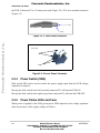
Power Switch (SW4) ...................................................................................... 2-4
Power Status LEDs and Fuse.......................................................................... 2-4
Selecting Terminal Baud Rate ........................................................................ 2-5
The Terminal Character Format ..................................................................... 2-5
Connecting the Terminal ................................................................................ 2-5
Using a Personal Computer as a Terminal...................................................... 2-5
System Power-up and Initial Operation.............................................................. 2-8
Using The BDM Port .......................................................................................... 2-8
Title
Chapter 3
Using the Monitor/Debug Firmware
3.1
3.2
3.2.1
3.2.2
3.2.2.1
3.2.2.2
3.2.2.3
3.3
3.4
3.5
3.5.1
3.5.2
3.5.3
3.5.4
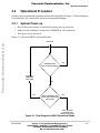
What Is dBUG?................................................................................................... 3-1
Operational Procedure ........................................................................................ 3-3
System Power-up ............................................................................................ 3-3
System Initialization ....................................................................................... 3-4
External RESET Button.............................................................................. 3-4
ABORT Button........................................................................................... 3-4
Software Reset Command .......................................................................... 3-4
Command Line Usage ........................................................................................ 3-5
Commands .......................................................................................................... 3-5
TRAP #15 Functions ........................................................................................ 3-40
OUT_CHAR ................................................................................................. 3-40
IN_CHAR ..................................................................................................... 3-41
CHAR_PRESENT ........................................................................................ 3-41
EXIT_TO_dBUG.......................................................................................... 3-41
Appendix A
Configuring dBUG for Network Downloads
A.1
A.2
A.3
Required Network Parameters ............................................................................ 1-1
Configuring dBUG Network Parameters............................................................ 1-2
Troubleshooting Network Problems ................................................................... 1-3
Appendix B
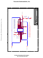
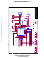
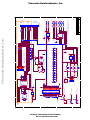
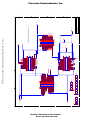
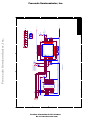
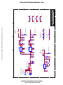
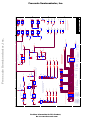
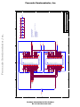
Schematics
Appendix C
Evaluation Board BOM
ii
M523xEVB User’s Manual
For More Information
On This
Product,
PRELIMINARY—SUBJECT
TO CHANGE
WITHOUT
NOTICE
Go to: www.freescale.com
MOTOROLA
Freescale Semiconductor, Inc.
ILLUSTRATIONS
Freescale Semiconductor, Inc...
Figure
Number
1-1
1-2
1-3
1-4
2-1
2-2
2-3
2-4
2-5
3-1
Title
Page
Number
M523xEVB Block Diagram ......................................................................................... 1-3
MCF5235 Block Diagram ............................................................................................ 1-5
External Memory Scheme ............................................................................................ 1-6
J1- BDM Connector Pin Assignment ......................................................................... 1-19
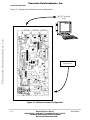
Minimum System Configuration .................................................................................. 2-2
2.1mm Power Connector .............................................................................................. 2-4
2-Lever Power Connector ............................................................................................. 2-4
Pin Assignment for Female (Terminal) Connector....................................................... 2-6
Jumper Locations .......................................................................................................... 2-7
Flow Diagram of dBUG Operational Mode ................................................................. 3-3
MOTOROLA
Illustrations
For More Information
On This
Product,
PRELIMINARY—SUBJECT
TO CHANGE
WITHOUT
NOTICE
Go to: www.freescale.com
iii
Freescale Semiconductor, Inc.
ILLUSTRATIONS
Title
Page
Number
Freescale Semiconductor, Inc...
Figure
Number
iv
M523xEVB User’s Manual
For More Information
On This
Product,
PRELIMINARY—SUBJECT
TO CHANGE
WITHOUT
NOTICE
Go to: www.freescale.com
MOTOROLA
Freescale Semiconductor, Inc.
Freescale Semiconductor, Inc...
TABLES
Table
Page
Title
Number
Number
1-1
M523x Product Family ................................................................................................. 1-1
1-2
The M523xEVB Default Memory Map........................................................................ 1-8
1-3
D[20:19] External Boot Chip Select Configuration ..................................................... 1-9
1-4
SW7-1 RCON ............................................................................................................... 1-9
1-5
SW7-2 JTAG_EN ......................................................................................................... 1-9
1-6
SW7-[4:3] Encoded Clock Mode ............................................................................... 1-10
1-7
SW7-5 Chip Configuration Mode............................................................................... 1-10
1-8
SW7-[7:6] Boot Device .............................................................................................. 1-10
1-9
SW7-8 Bus Drive Strength ......................................................................................... 1-10
1-10
SW7-[10:9] Address/Chip Select Mode ..................................................................... 1-10
1-11
M523xEVB Clock Source Selection .......................................................................... 1-11
1-12
UART2/FlexCAN1 Jumper Configuration................................................................. 1-14
1-13
FlexCAN1 Jumper Configuration............................................................................... 1-14
1-14
FlexCAN0 Jumper Configuration............................................................................... 1-15
1-15
CAN Bus Connector Pinout........................................................................................ 1-15
1-16
Ethernet/eTPU Jumper Configuration ........................................................................ 1-16
1-17
eTPU Header Pin Assignment .................................................................................... 1-17
1-18
USB DMA Enable and Disable Settings .................................................................... 1-21
1-19
J7................................................................................................................................. 1-21
1-20
J8................................................................................................................................. 1-22
1-21
J9................................................................................................................................. 1-23
1-22
J10............................................................................................................................... 1-24
1-23
User LEDs................................................................................................................... 1-26
1-24
LED Functions ............................................................................................................ 1-26
2-1
Power LEDs .................................................................................................................. 2-5
2-2
Pin Assignment for Female (Terminal) Connector....................................................... 2-6
3-1
dBUG Command Summary.......................................................................................... 3-6
C-1
MCF523xEVB BOM .................................................................................................... 3-1
MOTOROLA
Tables
For More Information
On This
Product,
PRELIMINARY—SUBJECT
TO CHANGE
WITHOUT
NOTICE
Go to: www.freescale.com
v
Freescale Semiconductor, Inc.
TABLES
Title
Page
Number
Freescale Semiconductor, Inc...
Table
Number
vi
M523xEVB User’s Manual
For More Information
On This
Product,
PRELIMINARY—SUBJECT
TO CHANGE
WITHOUT
NOTICE
Go to: www.freescale.com
MOTOROLA
Freescale Semiconductor, Inc.
Freescale Semiconductor, Inc...
Chapter 1
M523xEVB
This document details the setup and configuration of the ColdFire M523xEVB evaluation
board (hereafter referred to as the EVB). The EVB is intended to provide a mechanism for
easy customer evaluation of the MCF523x family of ColdFire microprocessors and to
facilitate hardware and software development. The EVB can be used by software and
hardware developers to test programs, tools, or circuits without having to develop a
complete microprocessor system themselves. All special features of the MCF523x family
are supported.
The heart of the evaluation board is the MCF5235, all the other M523x family members
have a subset of the MCF5235 specification and can therefore be fully emulated using the
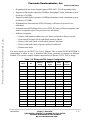
MCF5235 device. Table 1-1 below details the full product family.
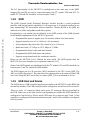
Table 1-1. M523x Product Family
Part Number
Package
eTPU
FEC
CRYPTO
CAN
MCF5232CAB80
160 QFP
16-channel
No
No
1
MCF5232CVM100
196 MAPBGA
16-channel
No
No
1
MCF5232CVM150
196 MAPBGA
16-channel
No
No
1
MCF5233CVM100
256 MAPBGA
32-channel
No
No
2
MCF5233CVM150
256 MAPBGA
32-channel
No
No
2
MCF5234CVM100
256 MAPBGA
16-channel
Yes
No
1
MCF5234CVM150
256 MAPBGA
16-channel
Yes
No
1
MCF5235CVM100
256 MAPBGA
16-channel
Yes
Yes
2
MCF5235CVM150
256 MAPBGA
16-channel
Yes
Yes
2
All of the devices in the same package are pin compatible.
The EVB provides for low cost software testing with the use of a ROM resident debug
monitor, dBUG, programmed into the external Flash device. Operation allows the user to
load code in the on-board RAM, execute applications, set breakpoints, and display or
modify registers or memory. No additional hardware or software is required for basic
operation.
MOTOROLA
Chapter 1. M523xEVB
PRELIMINARY—SUBJECT TO CHANGE WITHOUT NOTICE
For More Information On This Product,
Go to: www.freescale.com
1-1
Freescale Semiconductor, Inc.
Specifications
•
•
•
•
•
•
Motorola MCF5235 Microprocessor (150 MHz max core frequency)
External Clock source: 25 MHz
Operating temperature: 0°C to +70°C
Power requirement: 6–14V DC @ 300 ma Typical
Power output: 5V, 3.3V and 1.5V regulated supplies
Board Size: 10.00 × 5.40 inches, 8 layers
Freescale Semiconductor, Inc...
Memory Devices:
•
•
•
•
16-Mbyte SDRAM
2-Mbyte (512K × 16) Page Mode FLASH or 4-Mbyte (512K × 32) Page mode
FLASH
1-Mbyte ASRAM (optional)
64-Kbyte SRAM internal to MCF523x device
Peripherals:
•
•
•
•
•
•
•
•
•
•
Ethernet port 10/100Mb/s (Dual-Speed Fast Ethernet Transceiver, with MII)
UART0 (RS-232 serial port for dBUG firmware)
UART1 (auxiliary RS-232 serial port)
UART2 (auxiliary1 RS-232 serial port jumper selectable with FlexCAN1)
Enhanced Time Processor Unit (eTPU)
I2C interface
QSPI interface to ADC
FlexCan0 interface
USB Host and Device Interface
BDM/JTAG interface
User Interface:
•
•
•
•
•
•
•
1-2
Reset logic switch (debounced)
Boot logic selectable (dip switch)
Abort/IRQ7 logic switch (debounced)
PLL Clocking options - Oscillator, Crystal or SMA for external clocking signals
LEDs for power-up indication, general purpose I/O, and timer output signals
Expansion connectors for daughter card
UNI-3 connector for motor control cards
M523xEVB User’s Manual
PRELIMINARY—SUBJECT TO CHANGE WITHOUT NOTICE
For More Information On This Product,
Go to: www.freescale.com
MOTOROLA
Freescale Semiconductor, Inc.
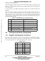
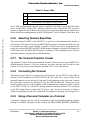
MCF5235 Microprocessor
Software:
•
Resident firmware package that provides a self-contained programming and
operating environment (dBUG)
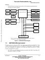
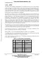
DB-9 (2)
connector
RS-232
transceivers (2)
RJ-45
connector
Ethernet
Transceiver*
26-pin Debug Header
ColdFire MCF523X
Clocking
circuitry
25 MHz
Osc.
USB 2.0 Host & Device
DB-9
connector
RS-232 / CAN
Transceiver
Control Signals
CAN Transceiver
Address [23:0]
DB-9
connector
Data [31:0]
ADC
Peripheral signals
Freescale Semiconductor, Inc...
25 MHz
Osc.
ETPU Headers*
SDRAM
16 Mbytes
Flash
2-4 Mbytes
ASRAM
1 Mbyte
(4) 60 pin Daughter Card
expansion connectors
*There is a jumper that allows the option of choosing between 16 eTPU channels
and Ethernet or 32 eTPU channels and no Ethernet
Figure 1-1. M523xEVB Block Diagram
1.1
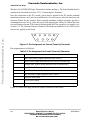
MCF5235 Microprocessor
The microprocessor used on the EVB is the highly integrated Motorola MCF5235 32-bit
ColdFire variable-length RISC processor. The MCF5235 implements a ColdFire Version 2
core with a maximum core frequency of 150 MHz and external bus speed of 75 MHz.
Features of the MCF5235 include:
•
V2 ColdFire core with enhanced multiply-accumulate unit (EMAC) providing 144
Dhrystone 2.1MIPS @ 150 MHz
MOTOROLA
Chapter 1. M523xEVB
PRELIMINARY—SUBJECT TO CHANGE WITHOUT NOTICE
For More Information On This Product,
Go to: www.freescale.com
1-3
Freescale Semiconductor, Inc.
MCF5235 Microprocessor
•
•
•
Freescale Semiconductor, Inc...
•
•
•
•
•
•
•
•
•
•
•
•
•
•
•
eTPU with 16 or 32 channels, 6 Kbytes of code memory and 1.5 Kbytes of data
memory with Nexus debug support
64 Kbytes of internal SRAM
External bus speed of one half the CPU operating frequency (75 MHz bus @
150 MHz core)
10/100 Mbps bus-mastering Ethernet controller
8 Kbytes of configurable instruction/data cache
Three universal asynchronous receiver/transmitters (UARTs) with DMA support
Controller area network 2.0B (FlexCAN module)
— Optional second FlexCAN module multiplexed with the third UART
Inter-integrated circuit (I2C) bus controller
Queued serial peripheral interface (QSPI) module
Hardware cryptography accelerator (optional)
— Random number generator
— DES/3DES/AES block cipher engine
— MD5/SHA-1/HMAC accelerator
Four channel 32-bit direct memory access (DMA) controller
Four channel 32-bit input capture/output compare timers with optional DMA
support
Four channel 16-bit periodic interrupt timers (PITs)
Programmable software watchdog timer
Interrupt controller capable of handling up to 126 interrupt sources
Clock module with Phase Locked Loop (PLL)
External bus interface module including a 2-bank synchronous DRAM controller
32-bit non-multiplexed bus with up to 8 chip select signals that support page-mode
FLASH memories
The MCF5235 communicates with external devices over a 32-bit wide data bus, D[31:0].
The MCF5235 can address a 32 bit address range. However, only 24 bits are available on
the external bus A[23:0]. There are internally generated chip selects to allow the full 32 bit
address range to be selected. There are regions that can be decoded to allow supervisor,
user, instruction, and data each to have the 32-bit address range.
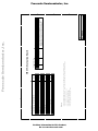
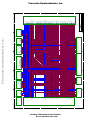
All the processor's signals are available via daughter card expansion connectors. Refer to
the schematic (Appendix B) for their pin assignments.
The MCF5235 processor has the capability to support both BDM and JTAG. These ports
are multiplexed and can be used with third party tools to allow the user to download code
1-4
M523xEVB User’s Manual
PRELIMINARY—SUBJECT TO CHANGE WITHOUT NOTICE
For More Information On This Product,
Go to: www.freescale.com
MOTOROLA
Freescale Semiconductor, Inc.
MCF5235 Microprocessor
to the board. The board is configured to boot up in the normal/BDM mode of operation. The
BDM signals are available at the port labeled BDM.
Freescale Semiconductor, Inc...
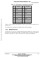
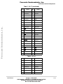
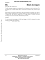
Figure 1-2 shows the MCF5235 processor block diagram.
MOTOROLA
Chapter 1. M523xEVB
PRELIMINARY—SUBJECT TO CHANGE WITHOUT NOTICE
For More Information On This Product,
Go to: www.freescale.com
1-5
Freescale Semiconductor, Inc.
MCF5235 Microprocessor
SDRAMC
QSPI
EIM
SDA
SCL
CHIP
SELECTS
(To/From SRAM backdoor)
UnTXD
UnRXD
UnRTS
EBI
INTC0
Arbiter
UnCTS
INTC1
TnOUT
TnIN
FAST
ETHERNET
CONTROLLER
(FEC)
UART
0
UART
1
UART
2
I2C
QSPI
SDRAMC
D[31:0]
(To/From PADI)
DTIM
0
4 CH DMA
DTIM
1
DTIM
2
A[23:0]
DTIM
3
R/W
CS[3:0]
(To/From
PADI)
TA
DREQ[2:0] DACK[2:0]
TSIZ[1:0]
JTAG_EN
BDM
MUX
Freescale Semiconductor, Inc...
(To/From PADI)
PADI
FEC
TEA
V2 ColdFire CPU
DIV
BS[3:0]
EMAC
JTAG
TAP
64 Kbytes
SRAM
(8Kx16)x4
Watchdog
Timer
MDHA
PORTS
(GPIO)
CIM
(To/From Arbiter)
SKHA
RNGA
8 Kbytes
CACHE
(1Kx32)x2
PLL
CLKGEN
PIT0
PIT1
PIT2
PIT3
(To/From INTC)
Edge
Port
Cryptography
Modules
Figure 1-2. MCF5235 Block Diagram
1-6
M523xEVB User’s Manual
PRELIMINARY—SUBJECT TO CHANGE WITHOUT NOTICE
For More Information On This Product,
Go to: www.freescale.com
MOTOROLA
Freescale Semiconductor, Inc.
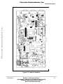
System Memory
1.2
System Memory
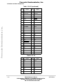
The following diagram shows the external memory implementation on the EVB.
MPU
Buffers
Data
ASRAM
(1 Mbyte)
Address
Freescale Semiconductor, Inc...
Control
SDRAM
(16 Mbytes)
Flash
(512K × 16
or
512K × 32)
Expansion
Connectors
Figure 1-3. External Memory Scheme
Note: The external bus interface signals to the external ASRAM and FLASH (and
USB) are buffered. This is in order not to exceed the maximum output load
capacitance of the microprocessor on the EVB.
The signals to the expansion connectors remain unbuffered to provide a “true”
interface to the user.
1.2.1
External Flash
The EVB is fitted with a single 512K × 16 page-mode FLASH memory (U19) giving a total
memory space of 2Mbytes. Alternatively a footprint is available for the EVB user to
upgrade this device to a 512K × 32 page-mode FLASH memory (U35), doubling the
memory size to 4Mbytes. Either U19 OR U35 should be fitted on the board - both devices
cannot be populated at the same time. Refer to the specific device data sheet and sample
software provided for configuring the FLASH memory.
Users should note that the debug monitor firmware is installed in this flash device.
Development tools or user application programs may erase or corrupt the debug monitor. If
the debug monitor becomes corrupted and it’s operation is desired, the firmware must be
programmed into the flash by applying a development port tool such as BDM. Users should
use caution to avoid this situation. The M523xEVB dBUG debugger/monitor firmware is
MOTOROLA
Chapter 1. M523xEVB
PRELIMINARY—SUBJECT TO CHANGE WITHOUT NOTICE
For More Information On This Product,
Go to: www.freescale.com
1-7
Freescale Semiconductor, Inc.
System Memory
programmed into the lower sectors of Flash (0xFFE0_0000 to 0xFFE2_FFFF for 2Mbytes
of FLASH or 0xFFC0_0000 to 0xFFC2_FFFF for 4 Mbytes of FLASH).
By default with U19 fitted on the EVB, jumper 64 (JP64) provides an alternative hardware
mechanism for write protection.
If the user has replaced U19 with the 32-bit FLASH device (U35), jumper 31 (JP31) has
the same functionality as JP64. U35 also has it’s own hardware write protect pin (C5) which
protects the bottom boot sector when pulled to ground.
Freescale Semiconductor, Inc...
1.2.2
SDRAM
The EVB is populated with 16 Mbytes of SDRAM. This is done with two devices (Micron
MT48LC4M16A2TG) each with a 16 bit data bus. Each device is organized as 1 Meg × 16
× 4 banks with a 16 bit data bus. One device stores the upper 16-bit word and the other the
lower 16 bit word of the MCF523x 32 bit data bus.
1.2.3
ASRAM
The EVB has a footprint for two 512K × 16 Asynchronous SRAM devices (Cypress
Semiconductor - CY7C1041CV3310ZC). These memory devices (U1 and U2) may be
populated by the user for benchmarking purposes.
Also see Section 1.2.5, “M523xEVB Memory Map”.
1.2.4
Internal SRAM
The MCF5235 processor has 64-Kbytes of internal SRAM memory which may be used as
data or instruction memory. This memory is mapped to 0x2000_0000 and configured as
data space but is not used by the dBUG monitor except during system initialization. After
system initialization is complete, the internal memory is available to the user. The memory
is relocatable to any 32-Kbyte boundary within the processor’s four gigabyte address space.
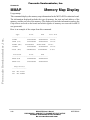
1.2.5
M523xEVB Memory Map
Interface signals to support the interface to external memory and peripheral devices are
generated by the memory controller. The MCF5235 supports 8 external chip selects,
CS[1:0] are used with external memories, CS2 is used for the USB controller and CS[7:3]
are easily accessible to users via the daughter card expansion connectors. CS0 also
functions as the global (boot) chip-select for booting out of external flash.
Since the MCF5235 chip selects are fully programmable, the memory banks may be located
at any 64-Kbyte boundary within the processor’s four gigabyte address space.
The default memory map for this board as configured by the Debug Monitor located in the
external FLASH bank can be found in table 1-2. The internal memory space of the
1-8
M523xEVB User’s Manual
PRELIMINARY—SUBJECT TO CHANGE WITHOUT NOTICE
For More Information On This Product,
Go to: www.freescale.com
MOTOROLA
Freescale Semiconductor, Inc.
System Memory
MCF5235 is detailed further in the MCF5235 Reference Manual. Chip Selects 0 and 1 can
be changed by user software to map the external memory in different locations but the chip
select configuration such as wait states and transfer acknowledge for each memory type
should be maintained.
Chip Select Usage:
External FLASH Memory
CS0
External ASRAM Memory
CS1
Table 1-2 shows the M523xEVB memory map.
Freescale Semiconductor, Inc...
Table 1-2. The M523xEVB Default Memory Map
Address Range
1.2.5.1
Signal and Device
0x0000_0000–0x00FF_FFFF
16 Mbyte SDRAM
0x2000_0000–0x2000_FFFF
64 Kbytes Internal SRAM
0x3000_0000–0x300F_FFFF
External ASRAM (not fitted)
0xFFE0_0000–0xFFFF_FFFF
or
0xFFC0_0000–0xFFFF_FFFF
2 Mbytes External Flash
or
4 Mbytes External Flash
Reset Vector Mapping
Asserting the reset input signal to the processor causes a reset exception. The reset
exception has the highest priority of any exception; it provides for system initialization and
recovery from catastrophic failure. Reset also aborts any processing in progress when the
reset input is recognized. Processing cannot be recovered.
The reset exception places the processor in the supervisor mode by setting the S-bit and
disables tracing by clearing the T bit in the SR. This exception also clears the M-bit and sets
the processor’s interrupt priority mask in the SR to the highest level (level 7). Next, the
VBR is initialized to zero (0x00000000). The control registers specifying the operation of
any memories (e.g., cache and/or RAM modules) connected directly to the processor are
disabled.
Once the processor is granted the bus, it then performs two longword read bus cycles. The
first longword at address 0 is loaded into the stack pointer and the second longword at
address 4 is loaded into the program counter. After the initial instruction is fetched from
memory, program execution begins at the address in the PC. If an access error or address
error occurs before the first instruction is executed, the processor enters the fault-on-fault
halted state.
The Memory that the MCF5235 accesses at address 0 is determined at reset by sampling
D[20:19].
MOTOROLA
Chapter 1. M523xEVB
PRELIMINARY—SUBJECT TO CHANGE WITHOUT NOTICE
For More Information On This Product,
Go to: www.freescale.com
1-9
Freescale Semiconductor, Inc.
Support Logic
Table 1-3. D[20:19] External Boot Chip Select Configuration
Freescale Semiconductor, Inc...
D[19:18]
Boot Device/Data Port Size
00
External (32-bit)
01
External (16-bit)
10
External (8-bit)
11
External (32-bit)
1.3
Support Logic
1.3.1
Reset Logic
The reset logic provides system initialization. Reset occurs during power-on or via
assertion of the signal RESET which causes the MCF5235 to reset. RESET is triggered by
the reset switch (SW6) which resets the entire processor/system.
dBUG configures the MCF5235 microprocessor internal resources during initialization.
The contents of the exception table are copied to address 0x0000_0000 in the SDRAM. The
Software Watchdog Timer is disabled, the Bus Monitor is enabled, and the internal timers
are placed in a stop condition. A memory map for the entire board can be seen in Table 1-2.
If the external RCON pin is asserted (SW7-1 ON) during reset, then various chip functions,
including the reset configuration pin functions after reset, are configured according to the
levels driven onto the external data pins. See tables below on settings for reset
configurations.
If the RCON pin is not asserted (SW7-1 OFF) during reset, the chip configuration and the
reset configuration pin functions after reset are determined by the RCON register or fixed
defaults, regardless of the states of the external data pins.
Table 1-4. SW7-1 RCON
SW7-1
Reset Configuration
OFF
RCON not asserted, Default Chip configuration or RCON register settings
ON
RCON is asserted, Chip functions, including the reset configuration after reset,
are configured according to the levels driven onto the external data pins.
Table 1-5. SW7-2 JTAG_EN
SW1-2
1-10
JTAG Enable
OFF
JTAG interface enabled
ON
BDM interface enabled
M523xEVB User’s Manual
PRELIMINARY—SUBJECT TO CHANGE WITHOUT NOTICE
For More Information On This Product,
Go to: www.freescale.com
MOTOROLA
Freescale Semiconductor, Inc.
Support Logic
Table 1-6. SW7-[4:3] Encoded Clock Mode
SW7-3
SW7-4
Clock Mode
OFF
OFF
External clock mode- (PLL disabled)
OFF
ON
1:1 PLL
ON
OFF
Normal PLL mode with external clock reference
ON
ON
Normal PLL mode w/crystal oscillator reference
Table 1-7. SW7-5 Chip Configuration Mode
Freescale Semiconductor, Inc...
SW7-5
RCON (SW7-1)
Mode
OFF
ON
Reserved
ON
ON
Master
X
OFF
Master
Table 1-8. SW7-[7:6] Boot Device
SW7-6
SW7-7
RCON (SW7-1)
Boot Device
OFF
OFF
ON
External (32-bit)
OFF
ON
ON
External (16-bit)
ON
OFF
ON
External (8-bit)
ON
ON
ON
External (32-bit)
X
X
OFF
External (32-bit)
Table 1-9. SW7-8 Bus Drive Strength
SW7-8
RCON (SW7-1)
Drive Strength
OFF
ON
Partial Bus Drive
ON
ON
Full Bus Drive
X
OFF
Partial Bus Drive
Table 1-10. SW7-[10:9] Address/Chip Select Mode
SW7-9
SW7-10
RCON (SW7-1)
Mode
OFF
OFF
ON
PF[7:5] = /CS[6:4]
OFF
ON
ON
PF[7] = /CS6, PF[6:5] = A[22:21]
ON
OFF
ON
PF[7:6] = /CS[6:5], PF[5] = A21
ON
ON
ON
PF[7:5] = A[23:21]
X
X
OFF
PF[7:5] = A[23:21]
MOTOROLA
Chapter 1. M523xEVB
PRELIMINARY—SUBJECT TO CHANGE WITHOUT NOTICE
For More Information On This Product,
Go to: www.freescale.com
1-11
Freescale Semiconductor, Inc.
Support Logic
1.3.2
Clock Circuitry
The are three options to provide the clock to the CPU. These options can be configured by
setting JP[35:37]. See Table 1-11 below.
Freescale Semiconductor, Inc...
Table 1-11. M523xEVB Clock Source Selection
JP35
JP36
JP37
Clock Selection
1-2
1-2
ON
25 MHz Oscillator (default setting)
2-3
1-2
ON
25 MHz External Clock
X
2-3
OFF
25 MHz Crystal (not populated)
The 25-MHz oscillator (U23) also feeds the Ethernet chip (U11).
There is also a 12-MHz crystal feeding the USB controller (U33).
1.3.3
Watchdog Timer
The dBUG Firmware does NOT enable the watchdog timer on the MCF5235.
1.3.4
Exception Sources
The ColdFire® family of processors can receive seven levels of interrupt priorities. When
the processor receives an interrupt which has a higher priority than the current interrupt
mask (in the status register), it will perform an interrupt acknowledge cycle at the end of
the current instruction cycle. This interrupt acknowledge cycle indicates to the source of the
interrupt that the request is being acknowledged and the device should provide the proper
vector number to indicate where the service routine for this interrupt level is located. If the
source of interrupt is not capable of providing a vector, its interrupt should be set up as an
autovector interrupt which directs the processor to a predefined entry in the exception table
(refer to the MCF523x User's Manual).
The processor goes to an exception routine via the exception table. This table is stored in
the Flash EEPROM. The address of the table location is stored in the VBR. The dBUG
ROM monitor writes a copy of the exception table into the RAM starting at $00000000. To
set an exception vector, the user places the address of the exception handler in the
appropriate vector in the vector table located at $00000000 and then points the VBR to
$00000000.
The MCF5235 microprocessor has seven external interrupt request lines IRQ[7:1]. The
interrupt controller is capable of providing up to 63 interrupt sources. These sources are:•
•
•
1-12
External interrupt signals IRQ[7:1] (EPORT)
Software watchdog timer module
Timer modules
M523xEVB User’s Manual
PRELIMINARY—SUBJECT TO CHANGE WITHOUT NOTICE
For More Information On This Product,
Go to: www.freescale.com
MOTOROLA
Freescale Semiconductor, Inc.
Support Logic
Freescale Semiconductor, Inc...
•
•
•
•
•
•
•
•
•
UART modules 0, 1 and 2
I2C module
DMA module
QSPI module
FEC module
PIT
Security module
FlexCAN0 and FlexCAN1
eTPU
All external interrupt inputs are edge sensitive. The active level is programmable. An
interrupt request must be held valid until an IACK cycle starts to guarantee correct
processing. Each interrupt input can have it’s priority programmed by setting the xIPL[2:0]
bits in the Interrupt Control Registers.
No interrupt sources should have the same level and priority as another. Programming two
interrupt sources with the same level and priority can result in undefined operation.
The M523xEVB hardware uses IRQ7 to support the ABORT function using the ABORT
switch (SW5). This switch is used to force an interrupt (level 7, priority 3) if the user's
program execution should be aborted without issuing a RESET (refer to Chapter 2 for more
information on ABORT). Since the ABORT switch is not capable of generating a vector in
response to a level seven interrupt acknowledge from the processor, the dBUG programs
this interrupt request for autovector mode.
Refer to MCF523x User’s Manual for more information about the interrupt controller.
1.3.5
TA Generation
The processor starts a bus cycle by asserting CSx with the other control signals. The
processor then waits for a transfer acknowledgment (TA) either from within (Auto
acknowledge - AA mode) or from the externally addressed device before it can complete
the bus cycle. -TA is used to indicate the completion of the bus cycle. It also allows devices
with different access times to communicate with the processor properly asynchronously.
The MCF5235 processor, as part of the chip-select logic, has a built-in mechanism to
generate TA for all external devices which do not have the capability to generate this signal.
For example the Flash ROM cannot generate a TA signal. The chip-select logic is
programmed by the dBUG ROM Monitor to generate TA internally after a pre-programmed
number of wait states. In order to support future expansion of the M523xEVB, the TA input
of the processor is also connected to the Processor Expansion Bus (J9, pin 44). This allows
any expansion boards to assert this line to provide a TA signal to the processor. On the
expansion boards this signal should be generated through an open collector buffer with no
MOTOROLA
Chapter 1. M523xEVB
PRELIMINARY—SUBJECT TO CHANGE WITHOUT NOTICE
For More Information On This Product,
Go to: www.freescale.com
1-13
Freescale Semiconductor, Inc.
Communication Ports
pull-up resistor; a pull-up resistor is included on this board. All TA signals from expansion
boards should be connected to this line.
1.3.6
User’s Program
JP64 on the 16Mbit FLASH (U19) or JP31 if using 32Mbit FLASH (U35) allows users to
test code from boot/POR without having to overwrite the ROM Monitor.
When the jumper is set between pins 1 and 2, the behavior of the system is normal, dBUG
boots and then runs from 0xFFE00000 (0xFFC00000). When the jumper is set between
pins 2 and 3, the board boots from the top half of the FLASH (0xFFF00000).
Freescale Semiconductor, Inc...
Procedure:
1. Compile and link as though the code was to be placed at the base of the flash.
2. Set up the jumper JP64 (JP31) for Normal operation, pin1 connected to pin 2.
3. Download to SDRAM (If using serial or ethernet, start the ROM Monitor first. If
using BDM via a wiggler cable, download first, then start ROM Monitor by
pointing the program counter (PC) to 0xFFE00400(0xFFC00400) and run.)
4. In the ROM Monitor, execute the ’FL write <dest> <src> <bytes>’ command.
5. Move jumper JP64 (JP31) to pin 2 connected to pin 3 and push the reset button
(S2). User code should now be running from reset/POR.
1.4
Communication Ports
The EVB provides external communication interfaces for two UART serial ports, a
UART/FlexCAN1 port, FlexCan0 port, QSPI, I2C port, 10/100T ethernet port, eTPU port
(including UNI3 and HS/ENCO connectors for auxiliary motor control cards), USB Host
port, USB Device port, and BDM/JTAG port.
1.4.1
UART0 and UART1 Ports
The MCF5235 device has three built in UARTs, each with its own software programmable
baud rate generator. Two of these UART interfaces are brought out to RS232 transceivers.
One channel is the ROM Monitor to Terminal output and the other is available to the user.
The ROM Monitor programs the interrupt level for UART0 to Level 3, priority 2 and
autovector mode of operation. The interrupt level for UART1 is programmed to Level 3,
priority 1 and autovector mode of operation. The signals from these channels are available
on expansion connectors J7 and J8. The signals of UART0 and UART1 are passed through
the RS-232 transceivers (U30) & (U31) and are available on DB-9 connectors (P4) and
(P5).
Refer to the MCF523x User’s Manual for programming the UART’s and their register
maps.
1-14
M523xEVB User’s Manual
PRELIMINARY—SUBJECT TO CHANGE WITHOUT NOTICE
For More Information On This Product,
Go to: www.freescale.com
MOTOROLA
Freescale Semiconductor, Inc.
Communication Ports
1.4.2
UART2/FlexCAN1 Port
The third UART on the MCF5235 is multiplexed with the second FlexCAN (FlexCAN1)
module. As these two modules are multiplexed such that the user has access to one or the
other, the functionality on the EVB is jumper selectable. Table 1-12 shows the jumper
configuration to activate UART2 or FlexCAN1.
Freescale Semiconductor, Inc...
Table 1-12. UART2/FlexCAN1 Jumper Configuration
Jumper
UART2 Setting
FlexCAN1 Setting
JP7
1-2
2-3
JP12
1-2
2-3
JP25
2-3
X
JP26
2-3
X
JP50
2-3
1-2
JP51
2-3
1-2
JP52
2-3
1-2
The signals of UART2 are passed through RS-232 transceiver U32 and are jumper
selectable (for settings see Table 1-12) on DB-9 connector P6.
The CAN1TX and CAN1RX signals from FlexCAN1 are brought out to a 3.3-V CAN
transceiver (Texas Instruments - SN65HVD230D) and are jumper selectable (for settings
see Table 1-12) on DB-9 connector P6. Jumpers JP3 and JP4 control the CAN hardware
configuration.
Table 1-13. FlexCAN1 Jumper Configuration
1.4.3
Jumper
Function
ON
OFF
JP3
Transceiver mode
Standby
High Speed (No Slope
Control)
JP4
CAN Termination
Terminating resistor
between CANL and CANH
No terminating resistor
FlexCAN0 Port
The EVB provides 1 dedicated CAN transceiver. The CAN0TX and CAN0RX signals are
brought out to a 3.3V CAN transceiver (Texas Instruments - SN65HVD230D). Jumper JP1
and JP2 control the CAN hardware configuration.
MOTOROLA
Chapter 1. M523xEVB
PRELIMINARY—SUBJECT TO CHANGE WITHOUT NOTICE
For More Information On This Product,
Go to: www.freescale.com
1-15
Freescale Semiconductor, Inc.
Communication Ports
Table 1-14. FlexCAN0 Jumper Configuration
Jumper
Function
ON
OFF
JP1
Transceiver mode
Standby
High Speed (No Slope
Control)
JP2
CAN Termination
Terminating resistor
between CANL and CANH
No terminating resistor
The CANL and CANH signals are brought out from the CAN transceiver to a female DB-9
connector (P1) in the configuration below.
Freescale Semiconductor, Inc...
Table 1-15. CAN Bus Connector Pinout
DB-9 pin
1.4.4
Signal
1,4-6,7-9
Not Connected
2
CANL
3
Ground
7
CANH
10/100T Ethernet Port
The MCF5235 microprocessor populated on the EVB is a superset device of the MCF523x
family. The upper 16 eTPU channels are multiplexed with the ethernet port giving the EVB
user the choice of utilizing either the full 32-channels of eTPU or 16-channels of eTPU with
the Fast Ethernet Controller (FEC) activated. Pin M4 on the MCF5235 configures the
internal functionality of these 16 pins. If the user is using the FEC, pin M4 must be pulled
low by setting SW7-11 to the ON position.
These 16 pins are also jumper selectable between the eTPU and the FEC in order to isolate
the external circuitry required to implement the functionality of these modules. Table 1-16
lists the appropriate jumper settings to enable eTPU or FEC functionality on these pins.
The MCF5235 device performs the full set of IEEE 802.3/Ethernet CSMA/CD media
access control and channel interface functions. The MCF5235 Ethernet Controller requires
an external interface adaptor and transceiver function to complete the interface to the
ethernet media. The MCF5235 Ethernet module also features an integrated fast (100baseT)
Ethernet media access controller (MAC).
The Fast Ethernet controller (FEC) incorporates the following features:
•
•
1-16
Support for three different Ethernet physical interfaces:
— 100-Mbps IEEE 802.3 MII
— 10-Mbps IEEE 802.3 MII
— 10-Mbps 7-wire interface (industry standard)
IEEE 802.3 full duplex flow control
M523xEVB User’s Manual
PRELIMINARY—SUBJECT TO CHANGE WITHOUT NOTICE
For More Information On This Product,
Go to: www.freescale.com
MOTOROLA
Freescale Semiconductor, Inc.
Communication Ports
•
•
•
•
•
Freescale Semiconductor, Inc...
•
Programmable max frame length supports IEEE 802.1 VLAN tags and priority
Support for full-duplex operation (200Mbps throughput) with a minimum system
clock rate of 50 MHz
Support for half-duplex operation (100Mbps throughput) with a minimum system
clock rate of 25 MHz
Retransmission from transmit FIFO following a collision (no processor bus
utilization)
Automatic internal flushing of the receive FIFO for runts (collision fragments) and
address recognition rejects (no processor bus utilization)
Address recognition
— Frames with broadcast address may be always accepted or always rejected
— Exact match for single 48-bit individual (unicast) address
— Hash (64-bit hash) check of individual (unicast) addresses
— Hash (64-bit hash) check of group (multicast) addresses
— Promiscuous mode
For more details see the MCF523x User’s Manual. The on board ROM MONITOR is
programmed to allow a user to download files from a network to memory in different
formats. The current compiler formats supported are S-Record, COFF, ELF or Image.
Table 1-16. Ethernet/eTPU Jumper Configuration
Jumper
MOTOROLA
Ethernet
Setting
Pin
Ethernet
Signal
eTPU
Setting
eTPU
Channel
JP5
D5
2-3
ERXER
1-2
23
JP9
C5
2-3
ETXCLK
1-2
22
JP10
B5
2-3
ETXD2
1-2
18
JP11
A5
2-3
ETXD1
1-2
17
JP13
D6
2-3
ETXEN
1-2
21
JP14
C6
2-3
ETXER
1-2
20
JP15
B6
2-3
ETXD3
1-2
19
JP16
C4
2-3
ERXD0
1-2
24
JP17
B7
2-3
ETXD0
1-2
16
JP18
C3
2-3
ERXD1
1-2
25
JP19
D4
2-3
ERXD2
1-2
26
JP20
D3
2-3
ERXD3
1-2
27
JP21
E3
2-3
ERXCLK
1-2
29
JP22
E4
2-3
ERXDV
1-2
28
JP23
F3
2-3
ECOL
1-2
31
JP24
F4
2-3
ECRS
1-2
30
Chapter 1. M523xEVB
PRELIMINARY—SUBJECT TO CHANGE WITHOUT NOTICE
For More Information On This Product,
Go to: www.freescale.com
1-17
Freescale Semiconductor, Inc.
Communication Ports
1.4.5
eTPU
Freescale Semiconductor, Inc...
The eTPU is an intelligent programmable I/O controller with its own core and memory
system, allowing it to perform complex timing and I/O management independently of the
CPU. The eTPU is essentially a co-processor designed for timing control, I/O handling,
serial communications, motor control. and engine control applications and accesses data
without the host CPU’s intervention. Consequently, the host CPU setup and service times
for each timer event are minimized or eliminated.
The eTPU is an enhanced version of the TPU module implemented on the MC68332 and
MPC500 products. Enhancements of the eTPU include a more powerful processor which
handles high-level C code efficiently and allows for more functionality and increased
performance. Although there is no compatibility at microcode level, the eTPU maintains
several features of older TPU versions and is conceptually almost identical. The eTPU
library is a superset of the standard TPU library functions modified to take advantage of
enhancements in the eTPU. These, along with a C compiler, make it relatively easy to port
older applications. By providing source code for the Motorola library, it is possible for the
eTPU to support the users own function development.
The eTPU has up to 32 timer channels in addition to having 6 Kbytes of code memory and
1.5 Kbytes of data memory that stores software modules downloaded at boot time and that
can be mixed and matched as required for any specific application.
As mentioned in Section 1.4.4, “10/100T Ethernet Port,” the upper 16-channels of the
eTPU are multiplexed with the Fast Ethernet Controller.
Refer to Table 1-16 to set the appropriate jumpers to enable 16 or 32-channels.
To configure the device to operate with the top 16-channels of the eTPU activated, pin M4
must be pulled high by setting SW7-11 to the OFF position.
All 32 eTPU channels are available on a 0.1” 2x20 Molex connector providing easy access
to the eTPU for the EVB user.
Table 1-17. eTPU Header Pin Assignment
Pin
1-18
eTPU Signal
Pin
eTPU Signal
1
+3.3V
2
+5V
3
TPUCH16
4
UTPUODIS
5
TPUCH17
6
LTPUODIS
7
TPUCH18
8
TPUCH0
9
TPUCH19
10
TPUCH1
11
TPUCH20
12
TPUCH2
13
TPUCH21
14
TPUCH3
15
TPUCH22
16
TPUCH4
M523xEVB User’s Manual
PRELIMINARY—SUBJECT TO CHANGE WITHOUT NOTICE
For More Information On This Product,
Go to: www.freescale.com
MOTOROLA
Freescale Semiconductor, Inc.
Communication Ports
Table 1-17. eTPU Header Pin Assignment (continued)
Freescale Semiconductor, Inc...
Pin
eTPU Signal
Pin
eTPU Signal
17
TPUCH23
18
TPUCH5
19
TPUCH24
20
TPUCH6
21
TPUCH25
22
TPUCH7
23
TPUCH26
24
TPUCH8
25
TPUCH27
26
TPUCH9
27
TPUCH28
28
TPUCH10
29
TPUCH29
30
TPUCH11
31
TPUCH30
32
TPUCH12
33
TPUCH31
34
TPUCH13
35
GND
36
TPUCH14
37
TCRCLK
38
TPUCH15
39
GND
40
GND
There is a UNI3 connector and HS/ENCO connector on the EVB for connection to an
auxiliary card.
The auxiliary card is intended for evaluation of the eTPU functionality.
1.4.6
BDM/JTAG Port
The MCF5235 processor has a Background Debug Mode (BDM) port, which supports
Real-Time Trace and Real-Time Debug. The signals which are necessary for debug are
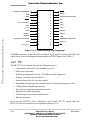
available at connector (J1). Figure 1-4 shows the (J1) Connector pin assignment.
MOTOROLA
Chapter 1. M523xEVB
PRELIMINARY—SUBJECT TO CHANGE WITHOUT NOTICE
For More Information On This Product,
Go to: www.freescale.com
1-19
Freescale Semiconductor, Inc.
Communication Ports
1
2
GND
3
4
GND
5
6
RESET
7
8
9
10
GND
11
12
PST2
13
14
PST0
15
16
DDATA2
17
18
DDATA1
DDATA0
19
20
GND
MOTOROLA RESERVED
21
22
MOTOROLA RESERVED
GND
23
24
Core Voltage
25
26
I/O or Pad Voltage
Freescale Semiconductor, Inc...
BKPT
DEVELOPER RESERVED
DSCLK
DEVELOPER RESERVED
DSI
DSO
PST3
PST1
DDATA3
PSTCLK
TA
Figure 1-4. J1- BDM Connector Pin Assignment
The BDM connector can also be used to interface to JTAG signals. On reset, the JTAG_EN
signal selects between multiplexed debug module and JTAG signals. See Table 1-5.
1.4.7
I2 C
The MCF5235’s I2C module includes the following features:
•
•
•
•
•
•
•
•
•
•
•
Compatibility with the I2C bus standard version 2.1
Multi master operation
Software programmable for one of 50 different clock frequencies
Software selectable acknowledge bit
Interrupt driven byte by byte data transfer
Arbitration-lost interrupt with automatic mode switching from master to slave
Calling address identification interrupt
Start and stop signal generation and detection
Repeated start signal generation
Acknowledge bit generation and detection
Bus busy detection
Please see the MCF523x User’s Manual for more detail. The I2C signals from the
MCF5235 device are brought out to expansion connector (J13).
1-20
M523xEVB User’s Manual
PRELIMINARY—SUBJECT TO CHANGE WITHOUT NOTICE
For More Information On This Product,
Go to: www.freescale.com
MOTOROLA
Freescale Semiconductor, Inc.
Communication Ports
The I2C functionality of the MCF5235 is multiplexed on the same pins as the QSPI.
Jumpers JP6 and JP8 are used to connect/disconnect the I2C signals, SDA and SCL. To
enable I2C JP6 and JP8 should be set between pins 2 and 3.
1.4.8
QSPI
Freescale Semiconductor, Inc...
The QSPI (Queued Serial Peripheral Interface) module provides a serial peripheral
interface with queued transfer capability. It will support up to 16 stacked transfers at one
time, minimizing CPU intervention between transfers. Transfer RAMs in the QSPI are
indirectly accessible using address and data registers.
Functionality is very similar, but not identical, to the QSPI portion of the QSM (Queued
Serial Module) implemented in the MC68332 processor.
•
•
•
•
•
•
•
Programmable queue to support up to 16 transfers without user intervention
Supports transfer sizes of 8 to 16 bits in 1-bit increments
Four peripheral chip-select lines for control of up to 15 devices
Baud rates from 147.1-Kbps to 18.75-Mbps at 75 MHz.
Programmable delays before and after transfers
Programmable QSPI clock phase and polarity
Supports wrap-around mode for continuous transfers
Please see the MCF523x User’s Manual for more detail. The QSPI signals from the
MCF5235 device are brought out to expansion connector (J12).
Some of the QSPI signals are multiplexed with the I2C module. JP6 and JP8 should be set
between pins 1 and 2 to enable the QSPI module.
The EVB features an A to D converter (ADC) interfaced to the CPU via the QSPI. The
ADC uses QSPI chip select 0. This chip select has a jumper that can be removed if the EVB
user is not using the ADC and wishes to connect QSPI_CS0 to an alternative device.
1.4.9
USB Host and Device
The EVB features a USB controller interfaced externally to the MCF5235 via the DMA and
external bus modules. The USB controller can be configured to run in Host or Device mode.
There is a series “A” connector (Host) and a series “B” connector (Device) populated on
the EVB. Either one or the other can be used depending on whether the USB controller is
configured to run in Host or Device mode. JP56 must be set between pins 2 and 3 if the
controller is configured in Host mode and between pin 1 and 2 if the controller is configured
in Device mode.
MOTOROLA
Chapter 1. M523xEVB
PRELIMINARY—SUBJECT TO CHANGE WITHOUT NOTICE
For More Information On This Product,
Go to: www.freescale.com
1-21
Freescale Semiconductor, Inc.
Connectors and User Components
The USB controller also has On-The-Go (OTG) functionality. There is a footprint on the
EVB for an OTG Mini-AB connector if the user wants to utilize USB OTG. If using OTG
JP55 must be fitted.
For more details see the Philips Semiconductor datasheet for the ISP1362 USB OTG
controller.
Freescale Semiconductor, Inc...
There are a series of jumpers connected to the USB controller that allow the user to
disconnect the DMA and interrupt signals between the CPU and the USB controller if the
USB controller is not in use. This gives the user access to the DMA timer module channels
1 and 2 and an extra interrupt signal if they do not require USB functionality. Table 1-18
details these jumper settings.
Table 1-18. USB DMA Enable and Disable Settings
Jumper
Functionality when Jumper is Fitted
Functionality when Jumper is NOT Fitted
JP57
USB DMA request signal
DMA Timer 1 input enabled
JP58
USB DMA request signal
DMA Timer 2 input enabled
JP59
USB DMA acknowledge signal
DMA Timer 1 output enabled
JP60
USB DMA acknowledge signal
DMA Timer 2 output enabled
JP61
Interrupt 4 enabled for USB
Interrupt 4 disabled from USB
JP62
DACK1 not in use - pulled high
DMA acknowledge 1 enabled
JP63
DACK 2 not in use - pulled high
DMA acknowledge 2 enabled
1.5
Connectors and User Components
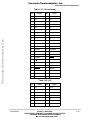
1.5.1
Daughter Card Expansion Connectors
Four, 60-way SMT connectors (J7, J8, J9 and J10) provide access to all MCF5235 signals.
These connectors are ideal for interfacing to a custom daughter card or for simple probing
of processor signals. Below is a pinout description of these connectors.
Table 1-19. J7
Pin
1-22
Signal
Pin
Signal
1
+5V
2
+5V
3
+3.3V
4
+3.3V
5
+3.3V
6
+3.3V
7
GND
8
GND
9
TPUCH24
10
TPUCH6
11
TPUCH17
12
TPUCH4
13
TPUCH18
14
TPUCH5
M523xEVB User’s Manual
PRELIMINARY—SUBJECT TO CHANGE WITHOUT NOTICE
For More Information On This Product,
Go to: www.freescale.com
MOTOROLA
Freescale Semiconductor, Inc.
Connectors and User Components
Table 1-19. J7 (continued)
Freescale Semiconductor, Inc...
Pin
Signal
Pin
Signal
15
TPUCH22
16
TPUCH2
17
TPUCH23
18
TPUCH3
19
TPUCH19
20
TPUCH1
21
TPUCH20
22
TPUCH0
23
TPUCH21
24
GND
25
TPUCH16
26
EMDIO
27
U2CTS
28
EMDC
29
I2C_SCL
30
I2C_SDA
31
QSPI_SCK
32
QSPI_DIN
33
BS3
34
QSPI_DOUT
35
BS2
36
QSPI_PCS0
37
BS1
38
SD_SCKE
39
BS0
40
CAN1RX
41
U2RTS
42
U2RXD
43
QSPI_PCS1
44
U1CTS
45
U1RTS
46
CAN1TX
47
U1RXD
48
U2TXD
49
U1TXD
50
CS2
51
CS3
52
CS7
53
CS6
54
CS5
55
CS1
56
CS0
57
CS4
58
A23
59
GND
60
GND
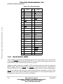
Table 1-20. J8
Pin
MOTOROLA
Signal
Pin
Signal
1
+5V
2
+1.5V
3
+3.3V
4
+3.3V
5
TPUCH8
6
TPUCH7
7
TPUCH10
8
TPUCH9
9
TPUCH25
10
TPUCH12
11
TPUCH27
12
TPUCH11
13
TPUCH26
14
TPUCH14
Chapter 1. M523xEVB
PRELIMINARY—SUBJECT TO CHANGE WITHOUT NOTICE
For More Information On This Product,
Go to: www.freescale.com
1-23
Freescale Semiconductor, Inc.
Connectors and User Components
Table 1-20. J8 (continued)
Freescale Semiconductor, Inc...
Pin
Signal
Pin
Signal
15
TPUCH29
16
TPUCH13
17
TPUCH28
18
TCRCLK
19
TPUCH31
20
TPUCH15
21
TPUCH30
22
GND
23
GND
24
U0CTS
25
U0RXD
26
DTOUT0
27
DTIN0
28
U0TXD
29
U0RTS
30
GND
31
CLKMOD0
32
+3.3V
33
CLKMOD1
34
GND
35
GND
36
D28
37
D30
38
D29
39
D31
40
D24
41
D26
42
D25
43
D27
44
D21
45
D23
46
D22
47
EXT_RSTIN
48
D19
49
GND
50
GND
51
D13
52
D20
53
D9
54
D17
55
D12
56
D18
57
D15
58
D16
59
GND
60
GND
Table 1-21. J9
Pin
1-24
Signal
Pin
Signal
1
+5V
2
+1.5V
3
+3.3V
4
+3.3V
5
+3.3V
6
+3.3V
7
GND
8
GND
9
A21
10
A22
11
A19
12
A20
13
A17
14
A18
M523xEVB User’s Manual
PRELIMINARY—SUBJECT TO CHANGE WITHOUT NOTICE
For More Information On This Product,
Go to: www.freescale.com
MOTOROLA
Freescale Semiconductor, Inc.
Connectors and User Components
Table 1-21. J9 (continued)
Freescale Semiconductor, Inc...
Pin
Signal
Pin
Signal
15
A16
16
A14
17
A15
18
A11
19
A13
20
GND
21
GND
22
A10
23
A12
24
A8
25
A9
26
A7
27
A6
28
A4
29
A5
30
GND
31
A2
32
A0
33
A3
34
A1
35
GND
36
GND
37
DTIN3
38
UTPUODIS
39
DTOUT3
40
LTPUODIS
41
TIP
42
TEA
43
TS
44
TA
45
CAN0RX
46
SD_WE
47
R/W
48
CAN0TX
49
SD_CAS
50
SD_CS0
51
CLKOUT
52
SD_RAS
53
SD_CS1
54
DDATA3
55
XTAL
56
EXTAL
57
GND
58
GND
59
GND
60
GND
Table 1-22. J10
Pin
MOTOROLA
Signal
Pin
Signal
1
+5V
2
+1.5V
3
+3.3V
4
+3.3V
5
D14
6
D10
7
D11
8
D6
9
D7
10
D8
11
D5
12
D4
13
GND
14
GND
Chapter 1. M523xEVB
PRELIMINARY—SUBJECT TO CHANGE WITHOUT NOTICE
For More Information On This Product,
Go to: www.freescale.com
1-25
Freescale Semiconductor, Inc.
Connectors and User Components
Table 1-22. J10 (continued)
Freescale Semiconductor, Inc...
Pin
1.5.2
Signal
Pin
Signal
15
D1
16
D2
17
D3
18
OE
19
D0
20
DTOUT1
21
DTIN1
22
+3.3V
23
+3.3V
24
IRQ6
25
IRQ7
26
TSIZ0
27
TSIZ1
28
IRQ2
29
IRQ3
30
IRQ4
31
IRQ5
32
TCLK/PSTCLK
33
DTOUT2
34
DTIN2
35
IRQ1
36
TDI/DSI
37
TDO/DSO
38
TMS/BKPT
39
TRST/DSCLK
40
GND
41
GND
42
PST3
43
PST1
44
PST2
45
PST0
46
DDATA0
47
DDATA2
48
DDATA1
49
GND
50
GND
51
JTAG_EN
52
RCON
53
GND
54
RSTOUT
55
GND
56
RESET
57
GND
58
GND
59
GND
60
GND
Reset Switch (SW6)
The reset logic provides system initilization. Reset occurs during power-on or via assertion
of the signal RESET which causes the MCF5235 to reset. Reset is also triggered by the reset
switch (SW6) which resets the entire processor/system.
A hard reset and voltage sense controller (U25) is used to produce an active low power-on
RESET signal. The reset switch SW6 is fed into U25 which generates the signal which is
fed to the MCF5235 reset, RESET. The RESET signal is an open collector signal and so
can be wire OR’ed with other reset signals from additional peripherals. On the EVB,
RESET is wire OR’d with the BDM reset signal and there is a reset signal brought out to
the expansion connectors for use with user hardware.
1-26
M523xEVB User’s Manual
PRELIMINARY—SUBJECT TO CHANGE WITHOUT NOTICE
For More Information On This Product,
Go to: www.freescale.com
MOTOROLA
Freescale Semiconductor, Inc.
Connectors and User Components
dBUG configures the MCF5235 microprocessor internal resources during initialization.
The instruction cache is invalidated and disabled. The Vector Base Register, VBR, contains
an address which initially points to the Flash memory. The contents of the exception table
are written to address $00000000 in the SDRAM. The Software Watchdog Timer is
disabled, the Bus Monitor is enabled, and the internal timers are placed in a stop condition.
The interrupt controller registers are initialized with unique interrupt level/priority pairs.
Freescale Semiconductor, Inc...
1.5.3
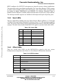
User LEDs
There are eight LEDs available to the user. Each of these LEDs are pulled to +3.3V through
a 10 ohm resistor and can be illuminated by driving a logic “0” on the appropriate signal to
“sink” the current. Each of these signals can be disconnected from it’s associated LED with
a jumper. The table below details which MCF5235 signal is associated with which LED.
Table 1-23. User LEDs
1.5.4
LED
MCF5235 Signal
Jumper to disconnect
D25
DTOUT0
JP38
D26
DTIN0
JP39
D27
DTOUT1
JP40
D28
DTIN1
JP41
D29
DTOUT2
JP42
D30
DTIN2
JP43
D31
DTOUT3
JP44
D32
DTIN3
JP45
Other LEDs
There are several other LED’s on the M523xEVB to signal to the user various
board/processor/component state. Below is a list of those LEDs and their functions:
Table 1-24. LED Functions
LED
Function
D1-D4
Ethernet Phy functionality
D5-D12
eTPU functionality
D14
+3.3V Power Good
D17
+5V Power Good
D21
+1.5V Power Good
D23
Abort (IRQ7) asserted
D24
Reset (RSTI) asserted
D25-D32
User LEDs (See Table 1-23)
MOTOROLA
Chapter 1. M523xEVB
PRELIMINARY—SUBJECT TO CHANGE WITHOUT NOTICE
For More Information On This Product,
Go to: www.freescale.com
1-27
Freescale Semiconductor, Inc.
Freescale Semiconductor, Inc...
Connectors and User Components
1-28
M523xEVB User’s Manual
PRELIMINARY—SUBJECT TO CHANGE WITHOUT NOTICE
For More Information On This Product,
Go to: www.freescale.com
MOTOROLA
Freescale Semiconductor, Inc.
Chapter 2
Initialization and Setup
Freescale Semiconductor, Inc...
2.1
System Configuration
The M523xEVB board requires the following items for minimum system configuration:
•
•
•
•
The M523xEVB board (provided).
Power supply, +6V to 14V DC with minimum of 300 mA.
RS232C compatible terminal or a PC with terminal emulation software.
RS232 Communication cable (provided).
MOTOROLA
Chapter 2. Initialization and Setup
PRELIMINARY—SUBJECT TO CHANGE WITHOUT NOTICE
For More Information On This Product,
Go to: www.freescale.com
2-1
Freescale Semiconductor, Inc.
System Configuration
Figure 2-1 displays the minimum system configuration.
RS-232 Terminal
Or PC
Freescale Semiconductor, Inc...
dBUG>
+7 to +14VDC
Input Power
Figure 2-1. Minimum System Configuration
2-2
M523xEVB User’s Manual
PRELIMINARY—SUBJECT TO CHANGE WITHOUT NOTICE
For More Information On This Product,
Go to: www.freescale.com
MOTOROLA
Freescale Semiconductor, Inc.
Installation and Setup
2.2
Installation and Setup
The following sections describe all the steps needed to prepare the board for operation.
Please read the following sections carefully before using the board. When you are preparing
the board for the first time, be sure to check that all jumpers are in the default locations.
Default jumper markings are documented on the master jumper table and printed on the
underside of the board. After the board is functional in its default mode, the Ethernet
interface may be used by following the instructions provided in Appendix A.
Freescale Semiconductor, Inc...
2.2.1
Unpacking
Unpack the computer board from its shipping box. Save the box for storing or reshipping.
Refer to the following list and verify that all the items are present. You should have
received:
•
•
•
•
•
•
•
M523xEVB Single Board Computer
M523xEVB User's Manual (this document)
One RS232 communication cable
One BDM (Background Debug Mode) “wiggler” cable
MCF5235RM ColdFire Integrated Microprocessor Reference Manual
ColdFire® Programmers Reference Manual
A selection of Third Party Developer Tools and Literature
NOTE
Avoid touching the MOS devices. Static discharge can and will
damage these devices.
Once you have verified that all the items are present, remove the board from its protective
jacket and anti-static bag. Check the board for any visible damage. Ensure that there are no
broken, damaged, or missing parts. If you have not received all the items listed above or
they are damaged, please contact Freescale Semiconductor immediately. For contact
details, please see the front of this manual.
2.2.2
Preparing the Board for Use
The board, as shipped, is ready to be connected to a terminal and power supply without any
need for modification. Figure 2-5 shows the position of the jumpers and connectors.
2.2.3
Providing Power to the Board
The EVB requires an external supply voltage of 7–14 V DC, minimum 1 Amp. This is
regulated on board using three switching voltage regulators to provide the necessary EVB
voltages of 5V, 3.3V and 1.5V. There are two different power supply input connectors on
MOTOROLA
Chapter 2. Initialization and Setup
PRELIMINARY—SUBJECT TO CHANGE WITHOUT NOTICE
For More Information On This Product,
Go to: www.freescale.com
2-3
Freescale Semiconductor, Inc.
Installation and Setup
the EVB. Connector P2 is a 2.1mm power jack (Figure 2-2), P3 a lever actuated connector
(Figure 2-3).
Freescale Semiconductor, Inc...
Figure 2-2. 2.1mm Power Connector
V+(7-14V)
GND
Figure 2-3. 2-Lever Power Connector
2.2.4
Power Switch (SW4)
Slide switch SW4 can be used to isolate the power supply input from the EVB voltage
regulators if required.
Moving the slide switch to the left (towards connector P3) will turn the EVB ON.
Moving the slide switch to the right (away from connector P3) will turn the EVB OFF.
2.2.5
Power Status LEDs and Fuse
When power is applied to the EVB, green power LEDs adjacent to the voltage regulators
show the presence of the supply voltage as follows:
2-4
M523xEVB User’s Manual
PRELIMINARY—SUBJECT TO CHANGE WITHOUT NOTICE
For More Information On This Product,
Go to: www.freescale.com
MOTOROLA
Freescale Semiconductor, Inc.
Installation and Setup
Table 2-1. Power LEDs
LED
Function
D17
Indicates that the +5V regulator is working correctly
D14
Indicates that the +3.3V regulator is working correctly
D21
Indicates that the +1.5V regulator is working correctly
Freescale Semiconductor, Inc...
If no LEDs are illuminated when the power is applied to the EVB, it is possible that either
power switch SW4 is in the “OFF” position or that the fuse F1 has blown. This can occur
if power is applied to the EVB in reverse-bias where a protection diode ensures that the fuse
blows rather than causing damage to the EVB. Replace F1 with a 20mm 1A fast blow fuse.
2.2.6
Selecting Terminal Baud Rate
The serial channel UART0 of the MCF5235 is used for serial communication and has a
built in timer. This timer is used by the dBUG ROM monitor to generate the baud rate used
to communicate with a serial terminal. A number of baud rates can be programmed. On
power-up or manual RESET, the dBUG ROM monitor firmware configures the channel for
19200 baud. Once the dBUG ROM monitor is running, a SET command may be issued to
select any baud rate supported by the ROM monitor.
2.2.7
The Terminal Character Format
The character format of the communication channel is fixed at power-up or RESET. The
default character format is 8 bits per character, no parity and one stop bit with no flow
control. It is necessary to ensure that the terminal or PC is set to this format.
2.2.8
Connecting the Terminal
The board is now ready to be connected to a PC/terminal. Use the RS-232 serial cable to
connect the PC/terminal to the M523xEVB PCB. The cable has a 9-pin female D-sub
terminal connector at one end and a 9-pin male D-sub connector at the other end. Connect
the 9-pin male connector to connector P4 on the M523xEVB board. Connect the 9-pin
female connector to one of the available serial communication channels normally referred
to as COM1 (COM2, etc.) on the PC running terminal emulation software. The connector
on the PC/terminal may be either male 25-pin or 9-pin. It may be necessary to obtain a
25pin-to-9pin adapter to make this connection. If an adapter is required, refer to Figure 2-4.
2.2.9
Using a Personal Computer as a Terminal
A personal computer may be used as a terminal provided a terminal emulation software
package is available. Examples of this software are PROCOMM, KERMIT, QMODEM,
MOTOROLA
Chapter 2. Initialization and Setup
PRELIMINARY—SUBJECT TO CHANGE WITHOUT NOTICE
For More Information On This Product,
Go to: www.freescale.com
2-5
Freescale Semiconductor, Inc.
Installation and Setup
Windows 95/98/2000/XP Hyper Terminal or similar packages. The board should then be
connected as described in Section 2.2.8, “Connecting the Terminal.”
Once the connection to the PC is made, power may be applied to the PC and the terminal
emulation software can be run. In terminal mode, it is necessary to select the baud rate and
character format for the channel. Most terminal emulation software packages provide a
command known as "Alt-p" (press the p key while pressing the Alt key) to choose the baud
rate and character format. The character format should be 8 bits, no parity, one stop bit. (see
section 1.9.5 The Terminal Character Format.) The baud rate should be set to 19200. Power
can now be applied to the board.
Freescale Semiconductor, Inc...
5
1
9
6
Figure 2-4. Pin Assignment for Female (Terminal) Connector
Pin assignments are as follows:
Table 2-2. Pin Assignment for Female (Terminal) Connector
DB9 Pin
Function
1
Data Carrier Detect, Output (shorted to pins 4 and 6)
2
Receive Data, Output from board (receive refers to terminal side)
3
Transmit Data, Input to board (transmit refers to terminal side)
4
Data Terminal Ready, Input (shorted to pin 1 and 6)
5
Signal Ground
6
Data Set Ready, Output (shorted to pins 1 and 4)
7
Request to Send, Input
8
Clear to send, Output
9
Not connected
Figure 2-5 on the next page shows the jumper locations for the board.
2-6
M523xEVB User’s Manual
PRELIMINARY—SUBJECT TO CHANGE WITHOUT NOTICE
For More Information On This Product,
Go to: www.freescale.com
MOTOROLA
Freescale Semiconductor, Inc.
Freescale Semiconductor, Inc...
Installation and Setup
Figure 2-5. Jumper Locations
MOTOROLA
Chapter 2. Initialization and Setup
PRELIMINARY—SUBJECT TO CHANGE WITHOUT NOTICE
For More Information On This Product,
Go to: www.freescale.com
2-7
Freescale Semiconductor, Inc.
System Power-up and Initial Operation
2.3
System Power-up and Initial Operation
When all of the cables are connected to the board, power may be applied. The dBUG ROM
Monitor initializes the board and then displays a power-up message on the terminal, which
includes the amount of memory present on the board.
Hard Reset
DRAM Size: 16M
Copyright 1995-2004 Motorola, Inc. All Rights Reserved.
ColdFire MCF523x EVS Firmware v2e.1a.xx (Build XXX on XXX
xx:xx:xx)
XX 20XX
Freescale Semiconductor, Inc...
Enter ’help’ for help.
dBUG>
The board is now ready for operation under the control of the debugger as described in
Chapter 2. If you do not get the above response, perform the following checks:
1. Make sure that the power supply is properly configured for polarity, voltage level
and current capability (~1A) and is connected to the board.
2. Check that the terminal and board are set for the same character format and baud.
3. Press the RESET button to insure that the board has been initialized properly.
If you still are not receiving the proper response, your board may have been damaged.
Contact Freescale Semiconductor for further instructions, please see the beginning of this
manual for contact details.
2.4
Using The BDM Port
The MCF5235 microprocessor has a built in debug module referred to as BDM
(background debug module). In order to use BDM, simply connect the 26-pin debug
connector on the board, J1, to the P&E BDM wiggler cable provided in the kit. No special
setting is needed. Refer to the ColdFire® User's Manual BDM Section for additional
instructions.
NOTE
BDM functionality and use is supported via third party
developer software tools. Details may be found on the
CD-ROM included in this kit.
2-8
M523xEVB User’s Manual
PRELIMINARY—SUBJECT TO CHANGE WITHOUT NOTICE
For More Information On This Product,
Go to: www.freescale.com
MOTOROLA
Freescale Semiconductor, Inc.
Freescale Semiconductor, Inc...
Chapter 3
Using the Monitor/Debug Firmware
The M523xEVB single board computer has a resident firmware package that provides a
self-contained programming and operating environment. The firmware, named dBUG,
provides the user with monitor/debug interface, inline assembler and disassembly, program
download, register and memory manipulation, and I/O control functions. This chapter is a
how-to-use description of the dBUG package, including the user interface and command
structure.
3.1
What Is dBUG?
dBUG is a traditional ROM monitor/debugger that offers a comfortable and intuitive
command line interface that can be used to download and execute code. It contains all the
primary features needed in a debugger to create a useful debugging environment.
The firmware provides a self-contained programming and operating environment. dBUG
interacts with the user through pre-defined commands that are entered via the terminal.
These commands are defined in Section 3.4, “Commands”.
The user interface to dBUG is the command line. A number of features have been
implemented to achieve an easy and intuitive command line interface.
dBUG assumes that an 80x24 character dumb-terminal is utilized to connect to the
debugger. For serial communications, dBUG requires eight data bits, no parity, and one stop
bit (8-N-1) with no flow control. The default baud rate is 19200 but can be changed after
power-up.
The command line prompt is “dBUG> ”. Any dBUG command may be entered from this
prompt. dBUG does not allow command lines to exceed 80 characters. Wherever possible,
dBUG displays data in 80 columns or less. dBUG echoes each character as it is typed,
eliminating the need for any “local echo” on the terminal side.
In general, dBUG is not case sensitive. Commands may be entered either in upper or lower
case, depending upon the user’s equipment and preference. Only symbol names require that
the exact case be used.
MOTOROLA
Chapter 3. Using the Monitor/Debug Firmware
PRELIMINARY—SUBJECT TO CHANGE WITHOUT NOTICE
For More Information On This Product,
Go to: www.freescale.com
3-1
Freescale Semiconductor, Inc.
What Is dBUG?
Most commands can be recognized by using an abbreviated name. For instance, entering
“h” is the same as entering “help”. Thus, it is not necessary to type the entire command
name.
The commands DI, GO, MD, STEP and TRACE are used repeatedly when debugging.
dBUG recognizes this and allows for repeated execution of these commands with minimal
typing. After a command is entered, simply press <RETURN> or <ENTER> to invoke the
command again. The command is executed as if no command line parameters were
provided.
Freescale Semiconductor, Inc...
An additional function called the "System Call" allows the user program to utilize various
routines within dBUG. The System Call is discussed at the end of this chapter.
The operational mode of dBUG is demonstrated in Figure 3-1. After the system
initialization, the board waits for a command-line input from the user terminal. When a
proper command is entered, the operation continues in one of the two basic modes. If the
command causes execution of the user program, the dBUG firmware may or may not be
re-entered, at the discretion of the user’s program. For the alternate case, the command will
be executed under control of the dBUG firmware, and after command completion, the
system returns to command entry mode.
During command execution, additional user input may be required depending on the
command function.
For commands that accept an optional <width> to modify the memory access size, the valid
values are:
•
•
•
B 8-bit (byte) access
W 16-bit (word) access
L 32-bit (long) access
When no <width> option is provided, the default width is.W, 16-bit.
The core ColdFire® register set is maintained by dBUG. These are listed below:
•
•
•
•
A0-A7
D0-D7
PC
SR
All control registers on ColdFire® are not readable by the supervisor-programming model,
and thus not accessible via dBUG. User code may change these registers, but caution must
be exercised as changes may render dBUG inoperable.
A reference to “SP” (stack pointer) actually refers to general purpose address register
seven, “A7.”
3-2
M523xEVB User’s Manual
PRELIMINARY—SUBJECT TO CHANGE WITHOUT NOTICE
For More Information On This Product,
Go to: www.freescale.com
MOTOROLA
Freescale Semiconductor, Inc.
Operational Procedure
3.2
Operational Procedure
System power-up and initial operation are described in detail in Chapter 2. This information
is repeated here for convenience and to prevent possible damage.
3.2.1
•
•
•
System Power-up
Be sure the power supply is connected properly prior to power-up.
Make sure the terminal is connected to TERMINAL (P4) connector.
Turn power on to the board.
Freescale Semiconductor, Inc...
Figure 3-1 shows the dBUG operational mode.
INITIALIZE
COMMAND LINE
INPUT FROM TERMINAL
NO
EXECUTE
COMMAND
FUNCTION
YES
NO
DOES COMMAND LINE
CAUSE USER PROGRAM
EXECUTION
YES
JUMP TO USER
PROGRAM AND
BEGIN EXECUTION
Figure 3-1. Flow Diagram of dBUG Operational Mode
MOTOROLA
Chapter 3. Using the Monitor/Debug Firmware
PRELIMINARY—SUBJECT TO CHANGE WITHOUT NOTICE
For More Information On This Product,
Go to: www.freescale.com
3-3
Freescale Semiconductor, Inc.
Operational Procedure
3.2.2
System Initialization
After the EVB is powered-up and initialized, the terminal will display:
Hard Reset
DRAM Size: 16M
ColdFire MCF5235 on the M523xEVB
Firmware vXX.XX.XX (Build X on XXXX)
Copyright 1995-2004 Motorola, Inc.
All Rights Reserved.
Freescale Semiconductor, Inc...
Enter ’help’ for help.
dBUG>
Other means can be used to re-initialize the M523xEVB firmware. These means are
discussed in the following paragraphs.
3.2.2.1
External RESET Button
External RESET (SW6) is the red button. Depressing this button causes all processes to
terminate, resets the MCF5235 processor and board logic and restarts the dBUG firmware.
Pressing the RESET button would be the appropriate action if all else fails.
3.2.2.2
ABORT Button
ABORT (SW5) is the button located next to the RESET button. The abort function causes
an interrupt of the present processing (a level 7 interrupt on MCF5235) and gives control
to the dBUG firmware. This action differs from RESET in that no processor register or
memory contents are changed, the processor and peripherals are not reset, and dBUG is not
restarted. Also, in response to depressing the ABORT button, the contents of the MCF5235
core internal registers are displayed.
The abort function is most appropriate when software is being debugged. The user can
interrupt the processor without destroying the present state of the system. This is
accomplished by forcing a non-maskable interrupt that will call a dBUG routine that will
save the current state of the registers to shadow registers in the monitor for display to the
user. The user will be returned to the ROM monitor prompt after exception handling.
3.2.2.3
Software Reset Command
dBUG does have a command that causes the dBUG to restart as if a hardware reset was
invoked. The command is “RESET”.
3-4
M523xEVB User’s Manual
PRELIMINARY—SUBJECT TO CHANGE WITHOUT NOTICE
For More Information On This Product,
Go to: www.freescale.com
MOTOROLA
Freescale Semiconductor, Inc.
Command Line Usage
3.3
Command Line Usage
The user interface to dBUG is the command line. A number of features have been
implemented to achieve an easy and intuitive command line interface.
dBUG assumes that an 80x24 ASCII character dumb terminal is used to connect to the
debugger. For serial communications, dBUG requires eight data bits, no parity, and one stop
bit (8-N-1). The baud rate default is 19200 bps — a speed commonly available from
workstations, personal computers and dedicated terminals.
Freescale Semiconductor, Inc...
The command line prompt is: dBUG>
Any dBUG command may be entered from this prompt. dBUG does not allow command
lines to exceed 80 characters. Wherever possible, dBUG displays data in 80 columns or
less. dBUG echoes each character as it is typed, eliminating the need for any local echo on
the terminal side.
The <Backspace> and <Delete> keys are recognized as rub-out keys for correcting
typographical mistakes.
Command lines may be recalled using the <Control> U, <Control> D and <Control> R key
sequences. <Control> U and <Control> D cycle up and down through previous command
lines. <Control> R recalls and executes the last command line.
In general, dBUG is not case-sensitive. Commands may be entered either in uppercase or
lowercase, depending upon the user’s equipment and preference. Only symbol names
require that the exact case be used.
Most commands can be recognized by using an abbreviated name. For instance, entering h
is the same as entering help. Thus it is not necessary to type the entire command name.
The commands DI, GO, MD, STEP and TRACE are used repeatedly when debugging.
dBUG recognizes this and allows for repeated execution of these commands with minimal
typing. After a command is entered, press the <Return> or <Enter> key to invoke the
command again. The command is executed as if no command line parameters were
provided.
3.4
Commands
This section lists the commands that are available with all versions of dBUG. Some board
or CPU combinations may use additional commands not listed below.
MOTOROLA
Chapter 3. Using the Monitor/Debug Firmware
PRELIMINARY—SUBJECT TO CHANGE WITHOUT NOTICE
For More Information On This Product,
Go to: www.freescale.com
3-5
Freescale Semiconductor, Inc.
Commands
Table 3-1. dBUG Command Summary
Freescale Semiconductor, Inc...
Mnemonic
3-6
Syntax
Description
ASM
asm <<addr> stmt>
Assemble
BC
bc addr1 addr2 length
Block Compare
BF
bf <width> begin end data <inc>
Block Fill
BM
bm begin end dest
Block Move
BR
br addr <-r> <-c count> <-t trigger>
Breakpoint
BS
bs <width> begin end data
Block Search
DC
dc value
Data Convert
DI
di<addr>
Disassemble
DL
dl <offset>
Download Serial
DLDBUG
dldbug
Download dBUG
DN
dn <-c> <-e> <-i> <-s <-o offset>> <filename>
Download Network
FL
fl erase addr bytes
fl write dest src bytes
Flash Utilities
GO
go <addr>
Execute
GT
gt addr
Execute To
HELP
help <command>
Help
IRD
ird <module.register>
Internal Register Display
IRM
irm module.register data
Internal Register Modify
LR
lr<width> addr
Loop Read
LW
lw<width> addr data
Loop Write
MD
md<width> <begin> <end>
Memory Display
MM
mm<width> addr <data>
Memory Modify
MMAP
mmap
Memory Map Display
RD
rd <reg>
Register Display
RM
rm reg data
Register Modify
RESET
reset
Reset
SD
sd
Stack Dump
SET
set <option value>
Set Configurations
SHOW
show <option>
Show Configurations
STEP
step
Step (Over)
SYMBOL
symbol <symb> <-a symb value> <-r symb> -C|l|s> Symbol Management
TRACE
trace <num>
Trace (Into)
UP
up begin end filename
Upload Memory to File
VERSION
version
Show Version
M523xEVB User’s Manual
PRELIMINARY—SUBJECT TO CHANGE WITHOUT NOTICE
For More Information On This Product,
Go to: www.freescale.com
MOTOROLA
Freescale Semiconductor, Inc.
Commands
ASM
Assembler
Usage: ASM <<addr> stmt>
The ASM command is a primitive assembler. The <stmt> is assembled and the resulting
code placed at <addr>. This command has an interactive and non-interactive mode of
operation.
Freescale Semiconductor, Inc...
The value for address <addr> may be an absolute address specified as a hexadecimal value,
or a symbol name. The value for stmt must be valid assembler mnemonics for the CPU.
For the interactive mode, the user enters the command and the optional <addr>. If the
address is not specified, then the last address is used. The memory contents at the address
are disassembled, and the user prompted for the new assembly. If valid, the new assembly
is placed into memory, and the address incremented accordingly. If the assembly is not
valid, then memory is not modified, and an error message produced. In either case, memory
is disassembled and the process repeats.
The user may press the <Enter> or <Return> key to accept the current memory contents and
skip to the next instruction, or a enter period to quit the interactive mode.
In the non-interactive mode, the user specifies the address and the assembly statement on
the command line. The statement is then assembled, and if valid, placed into memory,
otherwise an error message is produced.
Examples:
To place a NOP instruction at address 0x00010000, the command is:
asm
10000 nop
To interactively assemble memory at address 0x00400000, the command is:
asm
MOTOROLA
400000
Chapter 3. Using the Monitor/Debug Firmware
PRELIMINARY—SUBJECT TO CHANGE WITHOUT NOTICE
For More Information On This Product,
Go to: www.freescale.com
3-7
Freescale Semiconductor, Inc.
Commands
BC
Block Compare
Usage:BC addr1 addr2 length
The BC command compares two contiguous blocks of memory on a byte by byte basis. The
first block starts at address addr1 and the second starts at address addr2, both of length
bytes.
Freescale Semiconductor, Inc...
If the blocks are not identical, the address of the first mismatch is displayed. The value for
addresses addr1 and addr2 may be an absolute address specified as a hexadecimal value or
a symbol name. The value for length may be a symbol name or a number converted
according to the user defined radix (hexadecimal by default).
Example:
To verify that the data starting at 0x20000 and ending at 0x30000 is identical to the data
starting at 0x80000, the command is:
bc
3-8
20000 80000 10000
M523xEVB User’s Manual
PRELIMINARY—SUBJECT TO CHANGE WITHOUT NOTICE
For More Information On This Product,
Go to: www.freescale.com
MOTOROLA
Freescale Semiconductor, Inc.
Commands
BF
Block Fill
Usage:BF<width> begin end data <inc>
The BF command fills a contiguous block of memory starting at address begin, stopping at
address end, with the value data. <Width> modifies the size of the data that is written. If no
<width> is specified, the default of word sized data is used.
Freescale Semiconductor, Inc...
The value for addresses begin and end may be an absolute address specified as a
hexadecimal value, or a symbol name. The value for data may be a symbol name, or a
number converted according to the user-defined radix, normally hexadecimal.
The optional value <inc> can be used to increment (or decrement) the data value during the
fill.
This command first aligns the starting address for the data access size, and then increments
the address accordingly during the operation. Thus, for the duration of the operation, this
command performs properly-aligned memory accesses.
Examples:
To fill a memory block starting at 0x00020000 and ending at 0x00040000 with the value
0x1234, the command is:
bf
20000 40000 1234
To fill a block of memory starting at 0x00020000 and ending at 0x0004000 with a byte
value of 0xAB, the command is:
bf.b
20000 40000 AB
To zero out the BSS section of the target code (defined by the symbols bss_start and
bss_end), the command is:
bf
bss_start bss_end 0
To fill a block of memory starting at 0x00020000 and ending at 0x00040000 with data that
increments by 2 for each <width>, the command is:
bf
MOTOROLA
20000 40000 0 2
Chapter 3. Using the Monitor/Debug Firmware
PRELIMINARY—SUBJECT TO CHANGE WITHOUT NOTICE
For More Information On This Product,
Go to: www.freescale.com
3-9
Freescale Semiconductor, Inc.
Commands
BM
Block Move
Usage:BM begin end dest
The BM command moves a contiguous block of memory starting at address begin and
stopping at address end to the new address dest. The BM command copies memory as a
series of bytes, and does not alter the original block.
The values for addresses begin, end, and dest may be absolute addresses specified as
hexadecimal values, or symbol names. If the destination address overlaps the block defined
by begin and end, an error message is produced and the command exits.
Freescale Semiconductor, Inc...
Examples:
To copy a block of memory starting at 0x00040000 and ending at 0x00080000 to the
location 0x00200000, the command is:
bm
40000 80000 200000
To copy the target code’s data section (defined by the symbols data_start and data_end) to
0x00200000, the command is:
bm
data_start data_end 200000
NOTE
Refer to “upuser” command for copying code/data into Flash
memory.
3-10
M523xEVB User’s Manual
PRELIMINARY—SUBJECT TO CHANGE WITHOUT NOTICE
For More Information On This Product,
Go to: www.freescale.com
MOTOROLA
Freescale Semiconductor, Inc.
Commands
BR
Breakpoints
Usage:BR addr <-r> <-c count> <-t trigger>
The BR command inserts or removes breakpoints at address addr. The value for addr may
be an absolute address specified as a hexadecimal value, or a symbol name. Count and
trigger are numbers converted according to the user-defined radix, normally hexadecimal.
If no argument is provided to the BR command, a listing of all defined breakpoints is
displayed.
Freescale Semiconductor, Inc...
The -r option to the BR command removes a breakpoint defined at address addr. If no
address is specified in conjunction with the -r option, then all breakpoints are removed.
Each time a breakpoint is encountered during the execution of target code, its count value
is incremented by one. By default, the initial count value for a breakpoint is zero, but the -c
option allows setting the initial count for the breakpoint.
Each time a breakpoint is encountered during the execution of target code, the count value
is compared against the trigger value. If the count value is equal to or greater than the trigger
value, a breakpoint is encountered and control returned to dBUG. By default, the initial
trigger value for a breakpoint is one, but the -t option allows setting the initial trigger for
the breakpoint.
If no address is specified in conjunction with the -c or -t options, then all breakpoints are
initialized to the values specified by the -c or -t option.
Examples:
To set a breakpoint at the C function main() (symbol _main; see “symbol” command), the
command is:
br
_main
When the target code is executed and the processor reaches main(), control will be returned
to dBUG.
To set a breakpoint at the C function bench() and set its trigger value to 3, the command is:
br
_bench -t 3
When the target code is executed, the processor must attempt to execute the function
bench() a third time before returning control back to dBUG.
To remove all breakpoints, the command is:
br
MOTOROLA
-r
Chapter 3. Using the Monitor/Debug Firmware
PRELIMINARY—SUBJECT TO CHANGE WITHOUT NOTICE
For More Information On This Product,
Go to: www.freescale.com
3-11
Freescale Semiconductor, Inc.
Commands
BS
Block Search
Usage:BS<width> begin end data
The BS command searches a contiguous block of memory starting at address begin,
stopping at address end, for the value data. <Width> modifies the size of the data that is
compared during the search. If no <width> is specified, the default of word sized data is
used.
Freescale Semiconductor, Inc...
The values for addresses begin and end may be absolute addresses specified as hexadecimal
values, or symbol names. The value for data may be a symbol name or a number converted
according to the user-defined radix, normally hexadecimal.
This command first aligns the starting address for the data access size, and then increments
the address accordingly during the operation. Thus, for the duration of the operation, this
command performs properly-aligned memory accesses.
Examples:
To search for the 16-bit value 0x1234 in the memory block starting at 0x00040000 and
ending at 0x00080000:
bs
40000 80000 1234
This reads the 16-bit word located at 0x00040000 and compares it against the 16-bit value
0x1234. If no match is found, then the address is incremented to 0x00040002 and the next
16-bit value is read and compared.
To search for the 32-bit value 0xABCD in the memory block starting at 0x00040000 and
ending at 0x00080000:
bs.l
40000 80000 ABCD
This reads the 32-bit word located at 0x00040000 and compares it against the 32-bit value
0x0000ABCD. If no match is found, then the address is incremented to 0x00040004 and
the next 32-bit value is read and compared.
3-12
M523xEVB User’s Manual
PRELIMINARY—SUBJECT TO CHANGE WITHOUT NOTICE
For More Information On This Product,
Go to: www.freescale.com
MOTOROLA
Freescale Semiconductor, Inc.
Commands
DC
Data Conversion
Usage:DC data
The DC command displays the hexadecimal or decimal value data in hexadecimal, binary,
and decimal notation.
The value for data may be a symbol name or an absolute value. If an absolute value passed
into the DC command is prefixed by ‘0x’, then data is interpreted as a hexadecimal value.
Otherwise data is interpreted as a decimal value.
All values are treated as 32-bit quantities.
Freescale Semiconductor, Inc...
Examples:
To display the decimal and binary equivalent of 0x1234, the command is:
dc
0x1234
To display the hexadecimal and binary equivalent of 1234, the command is:
dc
MOTOROLA
1234
Chapter 3. Using the Monitor/Debug Firmware
PRELIMINARY—SUBJECT TO CHANGE WITHOUT NOTICE
For More Information On This Product,
Go to: www.freescale.com
3-13
Freescale Semiconductor, Inc.
Commands
DI
Disassemble
Usage:DI <addr>
The DI command disassembles target code pointed to by addr. The value for addr may be
an absolute address specified as a hexadecimal value, or a symbol name.
Freescale Semiconductor, Inc...
Wherever possible, the disassembler will use information from the symbol table to produce
a more meaningful disassembly. This is especially useful for branch target addresses and
subroutine calls.
The DI command attempts to track the address of the last disassembled opcode. If no
address is provided to the DI command, then the DI command uses the address of the last
opcode that was disassembled.
The DI command is repeatable.
Examples:
To disassemble code that starts at 0x00040000, the command is:
di
40000
To disassemble code of the C function main(), the command is:
di
3-14
_main
M523xEVB User’s Manual
PRELIMINARY—SUBJECT TO CHANGE WITHOUT NOTICE
For More Information On This Product,
Go to: www.freescale.com
MOTOROLA
Freescale Semiconductor, Inc.
Commands
DL
Download Console
Usage:DL <offset>
The DL command performs an S-record download of data obtained from the console,
typically a serial port. The value for offset is converted according to the user-defined radix,
normally hexadecimal. Please reference the ColdFire Microprocessor Family
Programmer’s Reference Manual for details on the S-Record format.
Freescale Semiconductor, Inc...
If offset is provided, then the destination address of each S-record is adjusted by offset.
The DL command checks the destination download address for validity. If the destination
is an address outside the defined user space, then an error message is displayed and
downloading aborted.
If the S-record file contains the entry point address, then the program counter is set to reflect
this address.
Examples:
To download an S-record file through the serial port, the command is:
dl
To download an S-record file through the serial port, and add an offset to the destination
address of 0x40, the command is:
dl
MOTOROLA
0x40
Chapter 3. Using the Monitor/Debug Firmware
PRELIMINARY—SUBJECT TO CHANGE WITHOUT NOTICE
For More Information On This Product,
Go to: www.freescale.com
3-15
Freescale Semiconductor, Inc.
Commands
DLDBUG
Download dBUG
Usage:DL <offset>
The DLDBUG command is used to update the dBUG image in Flash. It erases the Flash
sectors containing the dBUG image, downloads a new dBUG image in S-record format
obtained from the console, and programs the new dBUG image into Flash.
Freescale Semiconductor, Inc...
When the DLDBUG command is issued, dBUG will prompt the user for verification before
any actions are taken. If the command is affirmed, the Flash is erased and the user is
prompted to begin sending the new dBUG S-record file. The file should be sent as a text
file with no special transfer protocol.
Use this command with extreme caution, as any error can render dBUG useless!
3-16
M523xEVB User’s Manual
PRELIMINARY—SUBJECT TO CHANGE WITHOUT NOTICE
For More Information On This Product,
Go to: www.freescale.com
MOTOROLA
Freescale Semiconductor, Inc.
Commands
DN
Download Network
Usage:DN <-c> <-e> <-i> <-s> <-o offset> <filename>
Freescale Semiconductor, Inc...
The DN command downloads code from the network. The DN command handle files
which are either S-record, COFF, ELF or Image formats. The DN command uses Trivial
File Transfer Protocol (TFTP) to transfer files from a network host.
In general, the type of file to be downloaded and the name of the file must be specified to
the DN command. The -c option indicates a COFF download, the -e option indicates an
ELF download, the -i option indicates an Image download, and the -s indicates an S-record
download. The -o option works only in conjunction with the -s option to indicate an
optional offset for S-record download. The filename is passed directly to the TFTP server
and therefore must be a valid filename on the server.
If neither of the -c, -e, -i, -s or filename options are specified, then a default filename and
filetype will be used. Default filename and filetype parameters are manipulated using the
SET and SHOW commands.
The DN command checks the destination download address for validity. If the destination
is an address outside the defined user space, then an error message is displayed and
downloading aborted.
For ELF and COFF files which contain symbolic debug information, the symbol tables are
extracted from the file during download and used by dBUG. Only global symbols are kept
in dBUG. The dBUG symbol table is not cleared prior to downloading, so it is the user’s
responsibility to clear the symbol table as necessary prior to downloading.
If an entry point address is specified in the S-record, COFF or ELF file, the program counter
is set accordingly.
Examples:
To download an S-record file with the name “srec.out”, the command is:
dn -s srec.out
To download a COFF file with the name “coff.out”, the command is:
dn -c coff.out
To download a file using the default filetype with the name “bench.out”, the command is:
dn bench.out
To download a file using the default filename and filetype, the command is:
dn
MOTOROLA
Chapter 3. Using the Monitor/Debug Firmware
PRELIMINARY—SUBJECT TO CHANGE WITHOUT NOTICE
For More Information On This Product,
Go to: www.freescale.com
3-17
Freescale Semiconductor, Inc.
Commands
FL
Flash Utilities
Info Usage: FL
Erase Usage: FL erase addr bytes
Write Usage: FL write dest src bytes
Freescale Semiconductor, Inc...
The FL command provides a set of flash utilities that will display information about the
Flash devices on the EVB, erase a specified range of Flash, or erase and program a specified
range of Flash.
When issued with no parameters, the FL command will display usage information as well
as device specific information for the Flash devices available. This information includes
size, address range, protected range, access size, and sector boundaries.
When the erase command is given, the FL command will attempt to erase the number of
bytes specified on the command line beginning at addr. If this range doesn’t start and end
on Flash sector boundaries, the range will be adjusted automatically and the user will be
prompted for verification before proceeding.
When the write command is given, the FL command will program the number of bytes
specified from src to dest. An erase of this region will first be attempted. As with the erase
command, if the Flash range to be programmed doesn’t start and end on Flash sector
boundaries, the range will be adjusted and the user will be prompted for verification before
the erase is performed. The specified range is also checked to insure that the entire
destination range is valid within the same Flash device and that the src and dest are not
within the same device.
3-18
M523xEVB User’s Manual
PRELIMINARY—SUBJECT TO CHANGE WITHOUT NOTICE
For More Information On This Product,
Go to: www.freescale.com
MOTOROLA
Freescale Semiconductor, Inc.
Commands
GO
Execute
Usage:GO <addr>
The GO command executes target code starting at address addr. The value for addr may be
an absolute address specified as a hexadecimal value, or a symbol name.
Freescale Semiconductor, Inc...
If no argument is provided, the GO command begins executing instructions at the current
program counter.
When the GO command is executed, all user-defined breakpoints are inserted into the target
code, and the context is switched to the target program. Control is only regained when the
target code encounters a breakpoint, illegal instruction, trap #15 exception, or other
exception which causes control to be handed back to dBUG.
The GO command is repeatable.
Examples:
To execute code at the current program counter, the command is:
go
To execute code at the C function main(), the command is:
go _main
To execute code at the address 0x00040000, the command is:
go 40000
MOTOROLA
Chapter 3. Using the Monitor/Debug Firmware
PRELIMINARY—SUBJECT TO CHANGE WITHOUT NOTICE
For More Information On This Product,
Go to: www.freescale.com
3-19
Freescale Semiconductor, Inc.
Commands
GT
Execute To
Usage:GT addr
The GT command inserts a temporary breakpoint at addr and then executes target code
starting at the current program counter. The value for addr may be an absolute address
specified as a hexadecimal value, or a symbol name.
Freescale Semiconductor, Inc...
When the GT command is executed, all breakpoints are inserted into the target code, and
the context is switched to the target program. Control is only regained when the target code
encounters a breakpoint, illegal instruction, or other exception which causes control to be
handed back to dBUG.
Examples:
To execute code up to the C function bench(), the command is:
gt _bench
3-20
M523xEVB User’s Manual
PRELIMINARY—SUBJECT TO CHANGE WITHOUT NOTICE
For More Information On This Product,
Go to: www.freescale.com
MOTOROLA
Freescale Semiconductor, Inc.
Commands
IRD
Internal Register Display
Usage:IRD <module.register>
This command displays the internal registers of different modules inside the MCF5235. In
the command line, module refers to the module name where the register is located and
register refers to the specific register to display.
Freescale Semiconductor, Inc...
The registers are organized according to the module to which they belong. Use the IRD
command without any parameters to get a list of all the valid modules. Refer to the
MCF5235 user’s manual for more information on these modules and the registers they
contain.
Example:
ird
MOTOROLA
sim.rsr
Chapter 3. Using the Monitor/Debug Firmware
PRELIMINARY—SUBJECT TO CHANGE WITHOUT NOTICE
For More Information On This Product,
Go to: www.freescale.com
3-21
Freescale Semiconductor, Inc.
Commands
IRM
Internal Register Modify
Usage:IRM module.register data
This command modifies the contents of the internal registers of different modules inside
the MCF5235. In the command line, module refers to the module name where the register
is located and register refers to the specific register to modify. The data parameter specifies
the new value to be written into the register.
.
Example:
Freescale Semiconductor, Inc...
To modify the TMR register of the first Timer module to the value 0x0021, the command is:
irm
3-22
timer1.tmr 0021
M523xEVB User’s Manual
PRELIMINARY—SUBJECT TO CHANGE WITHOUT NOTICE
For More Information On This Product,
Go to: www.freescale.com
MOTOROLA
Freescale Semiconductor, Inc.
Commands
HELP
Help
Usage:HELP <command>
The HELP command displays a brief syntax of the commands available within dBUG. In
addition, the address of where user code may start is given. If command is provided, then
a brief listing of the syntax of the specified command is displayed.
Examples:
To obtain a listing of all the commands available within dBUG, the command is:
help
Freescale Semiconductor, Inc...
To obtain help on the breakpoint command, the command is:
help br
MOTOROLA
Chapter 3. Using the Monitor/Debug Firmware
PRELIMINARY—SUBJECT TO CHANGE WITHOUT NOTICE
For More Information On This Product,
Go to: www.freescale.com
3-23
Freescale Semiconductor, Inc.
Commands
LR
Loop Read
Usage:LR<width> addr
The LR command continually reads the data at addr until a key is pressed. The optional
<width> specifies the size of the data to be read. If no <width> is specified, the command
defaults to reading word sized data.
Example:
To continually read the longword data from address 0x20000, the command is:
20000
Freescale Semiconductor, Inc...
lr.l
3-24
M523xEVB User’s Manual
PRELIMINARY—SUBJECT TO CHANGE WITHOUT NOTICE
For More Information On This Product,
Go to: www.freescale.com
MOTOROLA
Freescale Semiconductor, Inc.
Commands
LW
Loop Write
Usage:LW<width> addr data
The LW command continually writes data to addr. The optional width specifies the size of
the access to memory. The default access size is a word.
Examples:
To continually write the longword data 0x12345678 to address 0x20000, the command is:
lw.l
20000 12345678
Note that the following command writes 0x78 into memory:
20000 12345678
Freescale Semiconductor, Inc...
lw.b
MOTOROLA
Chapter 3. Using the Monitor/Debug Firmware
PRELIMINARY—SUBJECT TO CHANGE WITHOUT NOTICE
For More Information On This Product,
Go to: www.freescale.com
3-25
Freescale Semiconductor, Inc.
Commands
MD
Memory Display
Usage:MD<width> <begin> <end>
The MD command displays a contiguous block of memory starting at address begin and
stopping at address end. The values for addresses begin and end may be absolute addresses
specified as hexadecimal values, or symbol names. Width modifies the size of the data that
is displayed. If no <width> is specified, the default of word sized data is used.
Freescale Semiconductor, Inc...
Memory display starts at the address begin. If no beginning address is provided, the MD
command uses the last address that was displayed. If no ending address is provided, then
MD will display memory up to an address that is 128 beyond the starting address.
This command first aligns the starting address for the data access size, and then increments
the address accordingly during the operation. Thus, for the duration of the operation, this
command performs properly-aligned memory accesses.
Examples:
To display memory at address 0x00400000, the command is:
md 400000
To display memory in the data section (defined by the symbols data_start and data_end),
the command is:
md data_start
To display a range of bytes from 0x00040000 to 0x00050000, the command is:
md.b
40000 50000
To display a range of 32-bit values starting at 0x00040000 and ending at 0x00050000:
md.l
3-26
40000 50000
M523xEVB User’s Manual
PRELIMINARY—SUBJECT TO CHANGE WITHOUT NOTICE
For More Information On This Product,
Go to: www.freescale.com
MOTOROLA
Freescale Semiconductor, Inc.
Commands
MM
Memory Modify
Usage:MM<width> addr <data>
Freescale Semiconductor, Inc...
The MM command modifies memory at the address addr. The value for addr may be an
absolute address specified as a hexadecimal value, or a symbol name. Width specifies the
size of the data that is modified. If no <width> is specified, the default of word sized data
is used. The value for data may be a symbol name, or a number converted according to the
user-defined radix, normally hexadecimal.
If a value for data is provided, then the MM command immediately sets the contents of addr
to data. If no value for data is provided, then the MM command enters into a loop. The loop
obtains a value for data, sets the contents of the current address to data, increments the
address according to the data size, and repeats. The loop terminates when an invalid entry
for the data value is entered, i.e., a period.
This command first aligns the starting address for the data access size, and then increments
the address accordingly during the operation. Thus, for the duration of the operation, this
command performs properly-aligned memory accesses.
Examples:
To set the byte at location 0x00010000 to be 0xFF, the command is:
mm.b
10000 FF
To interactively modify memory beginning at 0x00010000, the command is:
mm
MOTOROLA
10000
Chapter 3. Using the Monitor/Debug Firmware
PRELIMINARY—SUBJECT TO CHANGE WITHOUT NOTICE
For More Information On This Product,
Go to: www.freescale.com
3-27
Freescale Semiconductor, Inc.
Commands
MMAP
Memory Map Display
Usage:mmap
This command displays the memory map information for the M523xEVB evaluation board.
The information displayed includes the type of memory, the start and end address of the
memory, and the port size of the memory. The display also includes information on how the
Chip-selects are used on the board and which regions of memory are reserved for dBUG
use (protected).
Here is an example of the output from this command:
Freescale Semiconductor, Inc...
Type
Start
End
Port Size
--------------------------------------------------SDRAM
0x00000000
0x00FFFFFF
32-bit
SRAM (Int)
0x20000000
0x2000FFFF
32-bit
ASRAM (Ext)
0x30000000
IPSBAR
0x40000000
0x3007FFFF
0x7FFFFFFF
Flash (Ext)
0xFFE00000
0xFFFFFFFF
Protected
Start
End
32-bit
32-bit
16-bit
---------------------------------------dBUG Code
0xFFE00000
0xFFE3FFFF
dBUG Data
0x00000000
0x0000FFFF
Chip Selects
---------------CS0
Ext Flash
CS1
Ext ASRAM
3-28
M523xEVB User’s Manual
PRELIMINARY—SUBJECT TO CHANGE WITHOUT NOTICE
For More Information On This Product,
Go to: www.freescale.com
MOTOROLA
Freescale Semiconductor, Inc.
Commands
RD
Register Display
Usage:RD <reg>
The RD command displays the register set of the target. If no argument for reg is provided,
then all registers are displayed. Otherwise, the value for reg is displayed.
dBUG preserves the registers by storing a copy of the register set in a buffer. The RD
command displays register values from the register buffer.
Examples:
Freescale Semiconductor, Inc...
To display all the registers and their values, the command is:
rd
To display only the program counter:
rd pc
Here is an example of the output from this command:
PC: 00000000 SR: 2000 [t.Sm.000...xnzvc]
An: 00000000 00000000 00000000 00000000 00000000 00000000 00000000 01000000
Dn: 00000000 00000000 00000000 00000000 00000000 00000000 00000000 00000000
MOTOROLA
Chapter 3. Using the Monitor/Debug Firmware
PRELIMINARY—SUBJECT TO CHANGE WITHOUT NOTICE
For More Information On This Product,
Go to: www.freescale.com
3-29
Freescale Semiconductor, Inc.
Commands
RM
Register Modify
Usage:RM reg data
The RM command modifies the contents of the register reg to data. The value for reg is
the name of the register, and the value for data may be a symbol name, or it is converted
according to the user-defined radix, normally hexadecimal.
dBUG preserves the registers by storing a copy of the register set in a buffer. The RM
command updates the copy of the register in the buffer. The actual value will not be written
to the register until target code is executed.
Freescale Semiconductor, Inc...
Examples:
To change register D0 on MC68000 and ColdFire to contain the value 0x1234, the
command is:
rm
3-30
D0 1234
M523xEVB User’s Manual
PRELIMINARY—SUBJECT TO CHANGE WITHOUT NOTICE
For More Information On This Product,
Go to: www.freescale.com
MOTOROLA
Freescale Semiconductor, Inc.
Commands
RESET
Reset the Board and dBUG
Usage:RESET
The RESET command resets the board and dBUG to their initial power-on states.
The RESET command executes the same sequence of code that occurs at power-on. If the
RESET command fails to reset the board adequately, cycle the power or press the reset
button.
Examples:
To reset the board and clear the dBUG data structures, the command is:
Freescale Semiconductor, Inc...
reset
MOTOROLA
Chapter 3. Using the Monitor/Debug Firmware
PRELIMINARY—SUBJECT TO CHANGE WITHOUT NOTICE
For More Information On This Product,
Go to: www.freescale.com
3-31
Freescale Semiconductor, Inc.
Commands
SD
Stack Dump
Usage:SD
Freescale Semiconductor, Inc...
The SD command displays a back trace of stack frames. This command is useful after some
user code has executed that creates stack frames (i.e. nested function calls). After control is
returned to dBUG, the SD command will decode the stack frames and display a trace of the
function calls.
3-32
M523xEVB User’s Manual
PRELIMINARY—SUBJECT TO CHANGE WITHOUT NOTICE
For More Information On This Product,
Go to: www.freescale.com
MOTOROLA
Freescale Semiconductor, Inc.
Commands
SET
Set Configurations
Usage: SET <option value>
The SET command allows the setting of user-configurable options within dBUG. With no
arguments, SET displays the options and values available. The SHOW command displays
the settings in the appropriate format. The standard set of options is listed below.
Freescale Semiconductor, Inc...
baud - This is the baud rate for the first serial port on the board. All communications
between dBUG and the user occur using either 9600 or 19200 bps, eight data bits, no parity,
and one stop bit, 8-N-1, with no flow control.
base - This is the default radix for use in converting a number from its ASCII text
representation to the internal quantity used by dBUG. The default is hexadecimal (base 16),
and other choices are binary (base 2), octal (base 8), and decimal (base 10).
client - This is the network Internet Protocol (IP) address of the board. For network
communications, the client IP is required to be set to a unique value, usually assigned by
your local network administrator.
server - This is the network IP address of the machine which contains files accessible via
TFTP. Your local network administrator will have this information and can assist in
properly configuring a TFTP server if one does not exist.
gateway - This is the network IP address of the gateway for your local subnetwork. If the
client IP address and server IP address are not on the same subnetwork, then this option
must be properly set. Your local network administrator will have this information.
netmask - This is the network address mask to determine if use of a gateway is required.
This field must be properly set. Your local network administrator will have this
information.
filename - This is the default filename to be used for network download if no name is
provided to the DN command.
filetype - This is the default filetype to be used for network download if no type is provided
to the DN command. Valid values are: “srecord”, “coff”, and “elf”.
mac - This is the ethernet Media Access Control (MAC) address (a.k.a hardware address)
for the evaluation board. This should be set to a unique value, and the most significant
nibble should always be even.
Examples: To set the baud rate of the board to be 19200, the command is:
set
baud 19200
NOTE
See the SHOW command for a display containing the correct
formatting of these options.
MOTOROLA
Chapter 3. Using the Monitor/Debug Firmware
PRELIMINARY—SUBJECT TO CHANGE WITHOUT NOTICE
For More Information On This Product,
Go to: www.freescale.com
3-33
Freescale Semiconductor, Inc.
Commands
SHOW
Show Configurations
Usage: SHOW <option>
The SHOW command displays the settings of the user-configurable options within dBUG.
When no option is provided, SHOW displays all options and values.
Examples:
To display all options and settings, the command is:
show
To display the current baud rate of the board, the command is:
Freescale Semiconductor, Inc...
show
baud
Here is an example of the output from a show command:
dBUG> show
base: 16
baud: 19200
server: 0.0.0.0
client: 0.0.0.0
gateway: 0.0.0.0
netmask: 255.255.255.0
filename: test.s19
filetype: S-Record
ethaddr: 00:CF:52:82:CF:01
3-34
M523xEVB User’s Manual
PRELIMINARY—SUBJECT TO CHANGE WITHOUT NOTICE
For More Information On This Product,
Go to: www.freescale.com
MOTOROLA
Freescale Semiconductor, Inc.
Commands
STEP
Step Over
Usage:STEP
The STEP command can be used to “step over” a subroutine call, rather than tracing every
instruction in the subroutine. The ST command sets a temporary breakpoint one instruction
beyond the current program counter and then executes the target code.
The STEP command can be used to “step over” BSR and JSR instructions.
Freescale Semiconductor, Inc...
The STEP command will work for other instructions as well, but note that if the STEP
command is used with an instruction that will not return, i.e. BRA, then the temporary
breakpoint may never be encountered and dBUG may never regain control.
Examples:
To pass over a subroutine call, the command is:
step
MOTOROLA
Chapter 3. Using the Monitor/Debug Firmware
PRELIMINARY—SUBJECT TO CHANGE WITHOUT NOTICE
For More Information On This Product,
Go to: www.freescale.com
3-35
Freescale Semiconductor, Inc.
Commands
SYMBOL
Symbol Name Management
Usage:SYMBOL <symb> <-a symb value> <-r symb> <-c|l|s>
The SYMBOL command adds or removes symbol names from the symbol table. If only a
symbol name is provided to the SYMBOL command, then the symbol table is searched for
a match on the symbol name and its information displayed.
The -a option adds a symbol name and its value into the symbol table. The -r option
removes a symbol name from the table.
Freescale Semiconductor, Inc...
The -c option clears the entire symbol table, the -l option lists the contents of the symbol
table, and the -s option displays usage information for the symbol table.
Symbol names contained in the symbol table are truncated to 31 characters. Any symbol
table lookups, either by the SYMBOL command or by the disassembler, will only use the
first 31 characters. Symbol names are case-sensitive.
Symbols can also be added to the symbol table via in-line assembly labels and ethernet
downloads of ELF formatted files.
Examples:
To define the symbol “main” to have the value 0x00040000, the command is:
symbol
-a main 40000
To remove the symbol “junk” from the table, the command is:
symbol
-r junk
To see how full the symbol table is, the command is:
symbol
-s
To display the symbol table, the command is:
symbol
3-36
-l
M523xEVB User’s Manual
PRELIMINARY—SUBJECT TO CHANGE WITHOUT NOTICE
For More Information On This Product,
Go to: www.freescale.com
MOTOROLA
Freescale Semiconductor, Inc.
Commands
TRACE
Trace Into
Usage:TRACE <num>
The TRACE command allows single-instruction execution. If num is provided, then num
instructions are executed before control is handed back to dBUG. The value for num is a
decimal number.
The TRACE command sets bits in the processors’ supervisor registers to achieve
single-instruction execution, and the target code executed. Control returns to dBUG after a
single-instruction execution of the target code.
Freescale Semiconductor, Inc...
This command is repeatable.
Examples:
To trace one instruction at the program counter, the command is:
tr
To trace 20 instructions from the program counter, the command is:
tr
MOTOROLA
20
Chapter 3. Using the Monitor/Debug Firmware
PRELIMINARY—SUBJECT TO CHANGE WITHOUT NOTICE
For More Information On This Product,
Go to: www.freescale.com
3-37
Freescale Semiconductor, Inc.
Commands
UP
Upload Data
Usage:UP begin end filename
Freescale Semiconductor, Inc...
The UP command uploads the data from a memory region (specified by begin and end) to
a file (specified by filename) over the network. The file created contains the raw binary data
from the specified memory region. The UP command uses the Trivial File Transfer
Protocol (TFTP) to transfer files to a network host.
3-38
M523xEVB User’s Manual
PRELIMINARY—SUBJECT TO CHANGE WITHOUT NOTICE
For More Information On This Product,
Go to: www.freescale.com
MOTOROLA
Freescale Semiconductor, Inc.
Commands
VERSION
Display dBUG Version
Usage:VERSION
The VERSION command displays the version information for dBUG. The dBUG version,
build number and build date are all given.
Freescale Semiconductor, Inc...
dBUG common
major and minor
revision
{
{
In this example, v 2b . 1c . 1a
{
The version number is separated by a decimal, for example, “v 2b.1c.1a”.
CPU major
and minor
revision
board major
and minor
revision
The version date is the day and time at which the entire dBUG monitor was compiled and
built.
Examples:
To display the version of the dBUG monitor, the command is:
version
MOTOROLA
Chapter 3. Using the Monitor/Debug Firmware
PRELIMINARY—SUBJECT TO CHANGE WITHOUT NOTICE
For More Information On This Product,
Go to: www.freescale.com
3-39
Freescale Semiconductor, Inc.
TRAP #15 Functions
3.5
TRAP #15 Functions
An additional utility within the dBUG firmware is a function called the TRAP 15 handler.
This function can be called by the user program to utilize various routines within the dBUG,
to perform a special task, and to return control to the dBUG. This section describes the
TRAP 15 handler and how it is used.
There are four TRAP #15 functions. These are: OUT_CHAR, IN_CHAR,
CHAR_PRESENT, and EXIT_TO_dBUG.
Freescale Semiconductor, Inc...
3.5.1
OUT_CHAR
This function ( function code 0x0013) sends a character, which is in the lower 8 bits of D1,
to the terminal.
Assembly example:
/* assume d1 contains the character */
move.l
#$0013,d0
Selects the function
TRAP
#15
The character in d1 is sent to terminal
C example:
void board_out_char (int ch)
{
/* If your C compiler produces a LINK/UNLK pair for this routine,
* then use the following code which takes this into account
*/
#if
l
/* LINK a6,#0 -- produced by C compiler */
asm (“ move.l8(a6),d1”);
asm (“ move.l#0x0013,d0”);
asm (“ trap#15”);
/* UNLK a6
/* put ‘ch’into d1 */
/* select the function */
/* make the call */
-- produced by C compiler */
#else
/*
*
If C compiler does not produce a LINK/UNLK pair, the use
the following code.
*/
asm (“ move.l4(sp),d1”);
asm (“ move.l#0x0013,d0”);
asm (“ trap#15”);
/* put ‘ch’into d1 */
/* select the function */
/* make the call */
#endif
}
3-40
M523xEVB User’s Manual
PRELIMINARY—SUBJECT TO CHANGE WITHOUT NOTICE
For More Information On This Product,
Go to: www.freescale.com
MOTOROLA
Freescale Semiconductor, Inc.
TRAP #15 Functions
3.5.2
IN_CHAR
This function (function code 0x0010) returns an input character (from terminal) to the
caller. The returned character is in D1.
Assembly example:
move.l
#$0010,d0
Select the function
trap
#15
Make the call, the input character is in d1.
C example:
int board_in_char (void)
Freescale Semiconductor, Inc...
{
asm (“ move.l#0x0010,d0”);
/* select the function */
asm (“ trap#15”);
/* make the call */
asm (“ move.ld1,d0”);
/* put the character in d0 */
}
3.5.3
CHAR_PRESENT
This function (function code 0x0014) checks if an input character is present to receive. A
value of zero is returned in D0 when no character is present. A non-zero value in D0 means
a character is present.
Assembly example:
move.l
#$0014,d0
trap
#15
Select the function
Make the call,
d0 contains the response (yes/no).
C example:
int board_char_present (void)
{
asm (“ move.l#0x0014,d0”);
/* select the function */
asm (“ trap#15”);
/* make the call */
}
3.5.4
EXIT_TO_dBUG
This function (function code 0x0000) transfers the control back to the dBUG, by
terminating the user code. The register context are preserved.
Assembly example:
move.l
#$0000,d0
Select the function
trap
#15
Make the call,
exit to dBUG.
C example:
MOTOROLA
Chapter 3. Using the Monitor/Debug Firmware
PRELIMINARY—SUBJECT TO CHANGE WITHOUT NOTICE
For More Information On This Product,
Go to: www.freescale.com
3-41
Freescale Semiconductor, Inc.
TRAP #15 Functions
void board_exit_to_dbug (void)
{
asm (“ move.l#0x0000,d0”);
/* select the function */
asm (“ trap#15”);
/* exit and transfer to dBUG */
Freescale Semiconductor, Inc...
}
3-42
M523xEVB User’s Manual
PRELIMINARY—SUBJECT TO CHANGE WITHOUT NOTICE
For More Information On This Product,
Go to: www.freescale.com
MOTOROLA
Freescale Semiconductor, Inc.
Freescale Semiconductor, Inc...
Appendix A
Configuring dBUG for Network
Downloads
The dBUG module has the ability to perform downloads over an Ethernet network using
the Trivial File Transfer Protocol, TFTP (NOTE: this requires a TFTP server to be running
on the host attached to the board). Prior to using this feature, several parameters are
required for network downloads to occur. The information that is required and the steps for
configuring dBUG are described below.
A.1
Required Network Parameters
For performing network downloads, dBUG needs 6 parameters; 4 are network-related, and
2 are download-related. The parameters are listed below, with the dBUG designation
following in parenthesis.
All computers connected to an Ethernet network running the IP protocol need 3
network-specific parameters. These parameters are:
•
•
•
Internet Protocol, IP, address for the computer (client IP),
IP address of the Gateway for non-local traffic (gateway IP), and
Network netmask for flagging traffic as local or non-local (netmask).
In addition, the dBUG network download command requires the following three
parameters:
•
•
•
IP address of the TFTP server (server IP),
Name of the file to download (filename),
Type of the file to download (filetype of S-record, COFF, ELF, or Image).
Your local system administrator can assign a unique IP address for the board, and also
provide you the IP addresses of the gateway, netmask, and TFTP server. Fill out the lines
below with this information.
Client IP: ___.___.___.___
Server IP: ___.___.___.___
Gateway: ___.___.___.___
Netmask: ___.___.___.___
MOTOROLA
(IP address of the board)
(IP address of the TFTP server)
(IP address of the gateway)
(Network netmask)
Appendix A. Configuring dBUG for Network Downloads
PRELIMINARY—SUBJECT TO CHANGE WITHOUT NOTICE
For More Information On This Product,
Go to: www.freescale.com
A-1
Freescale Semiconductor, Inc.
Configuring dBUG Network Parameters
A.2
Configuring dBUG Network Parameters
Once the network parameters have been obtained, the dBUG Rom Monitor must be
configured. The following commands are used to configure the network parameters.
Freescale Semiconductor, Inc...
set
set
set
set
set
client <client IP>
server <server IP>
gateway <gateway IP>
netmask <netmask>
mac <addr>
For example, the TFTP server is named ‘santafe’ and has IP address 123.45.67.1. The
board is assigned the IP address of 123.45.68.15. The gateway IP address is 123.45.68.250,
and the netmask is 255.255.255.0. The MAC address is chosen arbitrarily and is unique.
The commands to dBUG are:
set
set
set
set
set
client 123.45.68.15
server 123.45.67.1
gateway 123.45.68.250
netmask 255.255.255.0
mac 00:CF:52:82:EB:01
The last step is to inform dBUG of the name and type of the file to download. Prior to
giving the name of the file, keep in mind the following.
Most, if not all, TFTP servers will only permit access to files starting at a particular
sub-directory. (This is a security feature which prevents reading of arbitrary files by
unknown persons.) For example, SunOS uses the directory /tftp_boot as the default TFTP
directory. When specifying a filename to a SunOS TFTP server, all filenames are relative
to /tftp_boot. As a result, you normally will be required to copy the file to download into
the directory used by the TFTP server.
A default filename for network downloads is maintained by dBUG. To change the default
filename, use the command:
set filename <filename>
When using the Ethernet network for download, either S-record, COFF, ELF, or Image files
may be downloaded. A default filetype for network downloads is maintained by dBUG as
well. To change the default filetype, use the command:
set filetype <srecord|coff|elf|image>
Continuing with the above example, the compiler produces an executable COFF file,
‘a.out’. This file is copied to the /tftp_boot directory on the server with the command:
rcp a.out santafe:/tftp_boot/a.out
Change the default filename and filetype with the commands:
set filename a.out
set filetype coff
A-2
M523xEVB User’s Manual
PRELIMINARY—SUBJECT TO CHANGE WITHOUT NOTICE
For More Information On This Product,
Go to: www.freescale.com
MOTOROLA
Freescale Semiconductor, Inc.
Troubleshooting Network Problems
Finally, perform the network download with the ‘dn’ command. The network download
process uses the configured IP addresses and the default filename and filetype for initiating
a TFTP download from the TFTP server.
A.3
Troubleshooting Network Problems
Freescale Semiconductor, Inc...
Most problems related to network downloads are a direct result of improper configuration.
Verify that all IP addresses configured into dBUG are correct. This is accomplished via the
‘show ’command.
Using an IP address already assigned to another machine will cause dBUG network
download to fail, and probably other severe network problems. Make certain the client IP
address is unique for the board.
Check for proper insertion or connection of the network cable. Is the status LED lit
indicating that network traffic is present?
Check for proper configuration and operation of the TFTP server. Most Unix workstations
can execute a command named ‘tftp’ which can be used to connect to the TFTP server as
well. Is the default TFTP root directory present and readable?
If ‘ICMP_DESTINATION_UNREACHABLE’ or similar ICMP message appears, then a
serious error has occurred. Reset the board, and wait one minute for the TFTP server to
time out and terminate any open connections. Verify that the IP addresses for the server
and gateway are correct. Also verify that a TFTP server is running on the server.
MOTOROLA
Appendix A. Configuring dBUG for Network Downloads
PRELIMINARY—SUBJECT TO CHANGE WITHOUT NOTICE
For More Information On This Product,
Go to: www.freescale.com
A-3
Freescale Semiconductor, Inc.
Freescale Semiconductor, Inc...
Troubleshooting Network Problems
A-4
M523xEVB User’s Manual
PRELIMINARY—SUBJECT TO CHANGE WITHOUT NOTICE
For More Information On This Product,
Go to: www.freescale.com
MOTOROLA
Freescale Semiconductor, Inc.
Freescale Semiconductor, Inc...
Appendix B
Schematics
MOTOROLA
Appendix B. Schematics
PRELIMINARY—SUBJECT TO CHANGE WITHOUT NOTICE
For More Information On This Product,
Go to: www.freescale.com
B-1
For More Information On This Product,
Go to: www.freescale.com
A
B
C
D
4
5
SHEET 2
SHEET 3
SHEET 4
SHEET 5
SHEET 6
SHEET 7
SHEET 8
SHEET 9
SHEET 10
SHEET 11
SHEET 12
SHEET 13
SHEET 14
SHEET 15
SHEET 16
Revision Information
Rev
Date
0.0
02 Feb 04
A
05 Mar 04
B
30 Apr 04
- All test points are denoted TPx
- All Switches are denoted SWx
- All jumpers are denoted JPx
- All connectors are denoted Jx
4
3
- All decoupling caps greater than 0.1uF are X7R SMD 0805 unless otherwise stated
Designer
L. Anderson
P. Highton
L. Anderson
M523X Evaluation Board
3
- All decoupling caps less than 0.1uF are COG SMD 0805 unless otherwise stated
Notes:
HIERARCHICAL INTERCONNECTS
ASRAM MEMORY
ADDRESS AND DATA BUS BUFFERS
CAN INTERFACE
M523X CPU
DEBUG
ETHERNET INTERFACE
ETPU INTERFACE
EXPANSION CONNECTORS
FLASH MEMORY
POWER SUPPLY UNIT
RESET CONFIGURATION AND CLOCKING CIRCUITRY
SDRAM MEMORY
SERIAL I/O INTERFACE
USB INTERFACE
Table Of Contents:
5
1
2
Date:
Size
B
Title
Friday, April 30, 2004
1
Sheet
Document Number
SCH-20380 General Notes and Information
M523xEVB
1
Motorola SPS TSPG - TECD ColdFire Group
Comments
Provisional release
Added Metrowerks schematic part number and revision letter.
Removed alternative footprint for 90-pin SSOP 32-bit Flash and
replaced with 16-bit Flash, corrected RJ45 pinout and added
18Kohm pull-down resistors to U11 (ethernet transceiver).
2
Freescale Semiconductor, Inc...
of
16
Rev
B
A
B
C
D
Freescale Semiconductor, Inc.
For More Information On This Product,
Go to: www.freescale.com
A
B
C
Sheet 10
5
I2C_SDA
I2C_SCL
QSPI_SCK
QSPI_DIN
QSPI_DOUT
QSPI_PCS0
QSPI_PCS1
/EXT_RSTIN
/RESET
/RSTOUT
CLKOUT
EXTAL
XTAL
/U0RTS
/U0CTS
U0TXD
U0RXD
/U1RTS
/U1CTS
U1TXD
U1RXD
/U2RTS
/U2CTS
U2TXD
U2RXD
/SD_WE
SD_SCKE
/SD_CS1
/SD_CS0
/SD_RAS
/SD_CAS
CAN0RX
CAN0TX
CAN1RX
CAN1TX
CLKMOD[1:0]
/RCON
JTAG_EN
DTIN0
DTOUT0
DTIN1
DTOUT1
DTIN2
DTOUT2
DTIN3
DTOUT3
DDATA[3:0]
PST[3:0]
TMS/BKPT
TCLK/PSTCLK
TDI/DSI
TDO/DSO
TRST/DSCLK
EMDC
EMDIO
TPUCH[31:16]
TPUCH[15:0]
LTPUODIS
UTPUODIS
TCRCLK
/CS[7:0]
/OE
D[31:0]
R/W
/IRQ[7:1]
/TS
/TIP
/TA
/TEA
TSIZ0
TSIZ1
/BS[3:0]
A[23:0]
/OE
DTOUT2
DTIN2
DTOUT1
DTIN1
USB
B_D[31:0]
B_A[23:0]
/IRQ[7:1]
/CS[7:0]
Sheet16
TPUCH[31:16]
TPUCH[15:0]
LTPUODIS
UTPUODIS
TCRCLK
/SD_WE
SD_SCKE
CLKOUT
QSPI_SCK
QSPI_DIN
QSPI_DOUT
QSPI_PCS0
SDRAM
B_A[23:0]
B_D[31:0]
4
/SD_CS0
/SD_RAS
/SD_CAS
D[31:0]
Expansion Connectors
Sheet 14
A[23:0]
D
Buffers
Ethernet
B_A[23:0]
B_D[31:0]
R/W
/EXT_RSTIN
LTPUODIS
UTPUODIS
/OE
R/W
/TS
/TIP
/TA
/TEA
/BS[3:0]
TSIZ0
/CS[7:0]
TSIZ1
D[31:0]
/CS[7:0]
Reset Config & Clocks
/RSTOUT
/IRQ[7:1]
ETH_CLK
ETXD3
ETXD2
ETXD1
ETXD0
ETXCLK
ETXER
ETXEN
ERXD3
ERXD2
ERXD1
ERXD0
ERXCLK
ERXER
ERXDV
ECRS
ECOL
3
Debug
EMDIO
EMDC
DTIN0
DTOUT0
DTIN1
DTOUT1
DTIN2
DTOUT2
DTIN3
DTOUT3
Sheet 13
ETPU/ETH
/RSTOUT
CLKMOD[1:0]
/RCON
JTAG_EN
/BDM_RSTIN
/RESET
TMS/BKPT
TDI/DSI
TDO/DSO
TRST/DSCLK
CLKOUT
EXTAL
XTAL
/IRQ[7:1]
ETH_CLK
/TIP
/TEA
TSIZ0
TSIZ1
R/W
/OE
R/W
B_A[23:0]
B_D[31:0]
/CS[7:0]
/RSTOUT
Sheet 8
TRST/DSCLK
TDO/DSO
TDI/DSI
TCLK/PSTCLK
Serial I/O
I2C_SDA
I2C_SCL
3
/TA
CANL1
CANH1
Sheet 4
Sheet 7
CAN
2
CAN1TX
CAN1RX
4
/RSTOUT
/IRQ[7:1]
Sheet 9
BDM_/RSTIN
TMS/BKPT
DDATA[3:0]
QSPI_SCK
QSPI_DIN
QSPI_DOUT
QSPI_PCS0
QSPI_PCS1
eTPU
/U2RTS
/U2CTS
U2TXD
U2RXD
Sheet 11
CAN0TX
CAN0RX
2
Sheet 5
Sheet 15
/U1RTS
/U1CTS
U1TXD
U1RXD
Flash Memory
CANL1
CANH1
/U0RTS
/U0CTS
U0TXD
U0RXD
5
/BS[3:0]
Sheet 12
ASRAM
R/W
PSU
Date:
Size
C
Title
Sheet 6
ETPU/ETH
I2C_SDA
I2C_SCL
QSPI_SCK
QSPI_DIN
QSPI_DOUT
QSPI_PCS0
QSPI_PCS1
/RESET
/RSTOUT
CLKOUT
EXTAL
XTAL
/U0RTS
/U0CTS
U0TXD
U0RXD
/U1RTS
/U1CTS
U1TXD
U1RXD
/U2RTS
/U2CTS
U2TXD
U2RXD
/SD_WE
SD_SCKE
/SD_CS1
/SD_CS0
/SD_RAS
/SD_CAS
CAN0RX
CAN0TX
CAN1RX
CAN1TX
CLKMOD[1:0]
/RCON
JTAG_EN
DTIN0
DTOUT0
DTIN1
DTOUT1
DTIN2
DTOUT2
DTIN3
DTOUT3
DDATA[3:0]
PST[3:0]
TMS/BKPT
TCLK/PSTCLK
TDI/DSI
TDO/DSO
TRST/DSCLK
ECOL
ECRS
ERXDV
ERXER
ERXCLK
ERXD0
ERXD1
ERXD2
ERXD3
ETXEN
ETXER
ETXCLK
ETXD0
ETXD1
ETXD2
ETXD3
EMDC
EMDIO
TPUCH[31:16]
TPUCH[15:0]
LTPUODIS
UTPUODIS
TCRCLK
/CS[7:0]
/OE
D[31:0]
R/W
/IRQ[7:1]
/TS
/TIP
/TA
/TEA
TSIZ0
TSIZ1
/BS[3:0]
Friday, April 30, 2004
1
Document Number
SCH-20380 Hierarchical Block Diagram
Sheet
2
Motorola SPS TSPG - TECD ColdFire Group
ETPU/ETH
I2C_SDA
I2C_SCL
QSPI_SCK
QSPI_DIN
QSPI_DOUT
QSPI_PCS0
QSPI_PCS1
/RESET
/RSTOUT
CLKOUT
EXTAL
XTAL
/U0RTS
/U0CTS
U0TXD
U0RXD
/U1RTS
/U1CTS
U1TXD
U1RXD
/U2RTS
/U2CTS
U2TXD
U2RXD
/SD_WE
/SD_SCKE
/SD_CS1
/SD_CS0
/SD_RAS
/SD_CAS
CAN0RX
CAN0TX
CAN1RX
CAN1TX
CLKMOD[1:0]
/RCON
JTAG_EN
DTIN0
DTOUT0
DTIN1
DTOUT1
DTIN2
DTOUT2
DTIN3
DTOUT3
1
A[23:0]
CPU
DDATA[3:0]
PST[3:0]
TMS/BKPT
TCLK/PSTCLK
TDI/DSI
TDO/DSO
TRST/DSCLK
ECOL
ECRS
ERXDV
ERXER
ERXCLK
ERXD0
ERXD1
ERXD2
ERXD3
ETXEN
ETXER
ETXCLK
ETXD0
ETXD1
ETXD2
ETXD3
EMDC
EMDIO
TPUCH[31:16]
TPUCH[15:0]
LTPUODIS
UTPUODIS
TCRCLK
/CS[7:0]
/OE
D[31:0]
R/W
/IRQ[7:1]
/TS
/TIP
/TA
/TEA
TSIZ0
TSIZ1
/BS[3:0]
A[23:0]
M523xEVB
Sheet 3
B_A[23:0]
PST[3:0]
D[31:0]
A[23:0]
Freescale Semiconductor, Inc...
of
16
Rev
B
A
B
C
D
Freescale Semiconductor, Inc.
/BS[3:0]
B_D[31:0]
/CS[7:0]
/OE
D
For More Information On This Product,
Go to: www.freescale.com
A
B
C
C1
1nF
+3.3V
C2
1nF
5
C3
1nF
/CS[7:0]
C4
1nF
R/W
C5
0.1uF
/CS[7:0]
C6
0.1uF
B_D[31:0]
C7
0.1uF
/CS1
/CS1
C8
0.1uF
4
4
B_A7
B_A8
B_A9
B_A10
B_A11
B_D4
B_D5
B_D6
B_D7
B_D0
B_D1
B_D2
B_D3
B_A2
B_A3
B_A4
B_A5
B_A6
B_A7
B_A8
B_A9
B_A10
B_A11
B_D20
B_D21
B_D22
B_D23
B_D16
B_D17
B_D18
B_D19
B_A2
B_A3
B_A4
B_A5
B_A6
+3.3V
+3.3V
U1
A0
A1
A2
A3
A4
/CE
I/00
I/01
I/02
I/03
VCC
VSS
I/04
I/05
I/06
I/07
/WE
A5
A6
A7
A8
A9
A17
A16
A15
/OE
/BHE
/BLE
I/O15
I/O14
I/O13
I/O12
VSS
VCC
I/O11
I/O10
I/O9
I/O8
NC
A14
A13
A12
A11
A10
44
43
42
41
40
39
38
37
36
35
34
33
32
31
30
29
28
27
26
25
24
23
A0
A1
A2
A3
A4
/CE
I/00
I/01
I/02
I/03
VCC
VSS
I/04
I/05
I/06
I/07
/WE
A5
A6
A7
A8
A9
U2
A17
A16
A15
/OE
/BHE
/BLE
I/O15
I/O14
I/O13
I/O12
VSS
VCC
I/O11
I/O10
I/O9
I/O8
NC
A14
A13
A12
A11
A10
44
43
42
41
40
39
38
37
36
35
34
33
32
31
30
29
28
27
26
25
24
23
B_A[23:0]
B_D[31:0]
CY7C1041CV3310ZC
TSOP II
Do not populate
1
2
3
4
5
6
7
8
9
10
11
12
13
14
15
16
17
18
19
20
21
22
ASRAM Lower 16-bit word
B_A[23:0]
B_D[31:0]
CY7C1041CV3310ZC
TSOP II
Do not populate
1
2
3
4
5
6
7
8
9
10
11
12
13
14
15
16
17
18
19
20
21
22
ASRAM Upper 16-bit word
B_A[23:0]
B_A16
B_A15
B_A14
B_A13
B_A12
B_D11
B_D10
B_D9
B_D8
B_D15
B_D14
B_D13
B_D12
B_A19
B_A18
B_A17
+3.3V
B_A16
B_A15
B_A14
B_A13
B_A12
B_D27
B_D26
B_D25
B_D24
B_D31
B_D30
B_D29
B_D28
B_A19
B_A18
B_A17
+3.3V
3
3
/BS3
/BS2
/BS1
/BS0
/BS[3:0]
5
/OE
NOTE: /BS3 selects the most
significant byte lane access and
/BS0 the least significant.
/BS[3:0]
2
Date:
Size
B
Title
NOTE: Alternative ASRAM's with the same PCB footprint
and functionality are :- Renesas HM62W16255HCJP-12
Each ASRAM is 256K x 16bit (512KB)
Total ASRAM available = 1MB
B_A[23:0]
2
Freescale Semiconductor, Inc...
M523xEVB
Friday, April 30, 2004
Document Number
SCH-20380 Asynchronous SRAM
1
Sheet
3
Motorola SPS TSPG - TECD ColdFire Group
1
of
16
Rev
B
A
B
C
D
Freescale Semiconductor, Inc.
For More Information On This Product,
Go to: www.freescale.com
A
B
C
D
/CS[7:0]
/CS1
/CS0
/CS2
5
5
C
VCC
Y
AND Gate
SN74LVC1G11
A
GND
B
U5
R/W
D[31:0]
+3.3V
D[31:0]
4
D16
D17
D18
D19
D20
D21
D22
D23
D24
D25
D26
D27
D28
D29
D30
D31
D0
D1
D2
D3
D4
D5
D6
D7
D8
D9
D10
D11
D12
D13
D14
D15
4
GND
GND
GND
GND
VCC
VCC
VCC
VCC
1A1
1A2
1A3
1A4
1A5
1A6
1A7
1A8
2A1
2A2
2A3
2A4
2A5
2A6
2A7
2A8
GND
GND
GND
GND
VCC
VCC
VCC
VCC
1A1
1A2
1A3
1A4
1A5
1A6
1A7
1A8
2A1
2A2
2A3
2A4
2A5
2A6
2A7
2A8
MC74LCX16245DT
GND
GND
GND
GND
1DIR
1OE
2OE
2DIR
1B1
1B2
1B3
1B4
1B5
1B6
1B7
1B8
2B1
2B2
2B3
2B4
2B5
2B6
2B7
2B8
U6
MC74LCX16245DT
GND
GND
GND
GND
1DIR
1OE
2OE
2DIR
1B1
1B2
1B3
1B4
1B5
1B6
1B7
1B8
2B1
2B2
2B3
2B4
2B5
2B6
2B7
2B8
U3
28
34
39
45
7
18
31
42
47
46
44
43
41
40
38
37
36
35
33
32
30
29
27
26
28
34
39
45
7
18
31
42
47
46
44
43
41
40
38
37
36
35
33
32
30
29
27
26
DATA BUS TRANSCEIVERS
4
10
15
21
1
48
25
24
2
3
5
6
8
9
11
12
13
14
16
17
19
20
22
23
4
10
15
21
1
48
25
24
2
3
5
6
8
9
11
12
13
14
16
17
19
20
22
23
+3.3V
B_D16
B_D17
B_D18
B_D19
B_D20
B_D21
B_D22
B_D23
B_D24
B_D25
B_D26
B_D27
B_D28
B_D29
B_D30
B_D31
+3.3V
B_D0
B_D1
B_D2
B_D3
B_D4
B_D5
B_D6
B_D7
B_D8
B_D9
B_D10
B_D11
B_D12
B_D13
B_D14
B_D15
3
B_D[31:0]
3
1
3
5
7
1
3
5
7
A[23:0]
Address and Data Bus buffers/transceivers used to buffer
the signals for the ASRAM and Flash memories and the
USB controller.
B_D[31:0]
2
4
6
8
2
4
6
8
2
4x 4.7K
1
3
5
7
RP2
4x 4.7K
1
3
5
7
RP1
2
2
4
6
8
2
4
6
8
A[23:0]
A16
A17
A18
A19
A20
A21
A22
A23
A0
A1
A2
A3
A4
A5
A6
A7
A8
A9
A10
A11
A12
A13
A14
A15
C9
0.1uF
+3.3V
GND
GND
GND
GND
VCC
VCC
VCC
VCC
1A1
1A2
1A3
1A4
1A5
1A6
1A7
1A8
2A1
2A2
2A3
2A4
2A5
2A6
2A7
2A8
T/R
A0
A1
A2
A3
A4
A5
A6
A7
GND
MC74LCX245DT
VCC
OE
B0
B1
B2
B3
B4
B5
B6
B7
U7
1
2
3
4
5
6
7
8
9
10
Date:
Size
B
B_A16
B_A17
B_A18
B_A19
B_A20
B_A21
B_A22
B_A23
+3.3V
B_A0
B_A1
B_A2
B_A3
B_A4
B_A5
B_A6
B_A7
B_A8
B_A9
B_A10
B_A11
B_A12
B_A13
B_A14
B_A15
C13
1nF
C14
1nF
B_A[23:0]
1
Friday, April 30, 2004
1
Sheet
4
of
C15
1nF
Motorola SPS TSPG - TECD ColdFire Group
Document Number
SCH-20380 Buffers
M523xEVB
28
34
39
45
7
18
31
42
47
46
44
43
41
40
38
37
36
35
33
32
30
29
27
26
C12
1nF
MC74LCX16245DT
GND
GND
GND
GND
1DIR
1OE
2OE
2DIR
1B1
1B2
1B3
1B4
1B5
1B6
1B7
1B8
2B1
2B2
2B3
2B4
2B5
2B6
2B7
2B8
U4
C11
0.1uF
ADDRESS BUS BUFFERS
20
19
18
17
16
15
14
13
12
11
+3.3V
4
10
15
21
1
48
25
24
2
3
5
6
8
9
11
12
13
14
16
17
19
20
22
23
C10
0.1uF
Title
Freescale Semiconductor, Inc...
16
Rev
B
B_A[23:0]
A
B
C
D
Freescale Semiconductor, Inc.
For More Information On This Product,
Go to: www.freescale.com
A
B
C
D
C16
0.1uF
+3.3V
C17
0.1uF
5
5
C18
1nF
CAN1RX
CAN1TX
C19
1nF
CAN0RX
CAN0TX
+3.3V
1
2
3
4
D
GND
VCC
R
U9
+3.3V
4
U8
RS
CANH
CANL
VREF
8
7
6
5
8
7
6
5
1K
R1
1K
R3
JP3
2
Transceiver Mode
1
2
3
+3.3V
3
Transceiver Mode
1
JP1
Default setting for JP1 is NOT fitted.
Default setting for JP3 is NOT fitted.
SN65HVD230D
D
GND
VCC
R
RS
CANH
CANL
VREF
1
2
3
4
SN65HVD230D
4
+3.3V
62
R4
JP2
CANH1
CANL1
2
CAN Termination
JP4
Default setting for JP4 is fitted.
CAN Channel 1
1
2
2
CAN Termination
1
Default setting for JP2 is fitted.
CAN1 and UART2 share the same
DB9 connector on Sheet 15
62
R2
P1
CAN Channel 0
5
9
4
8
3
7
2
6
1
CAN Bus Connector
- 9 way D-type
(Female)
2
Freescale Semiconductor, Inc...
Date:
Size
B
Title
Friday, April 30, 2004
1
Sheet
5
Motorola SPS TSPG - TECD ColdFire Group
Document Number
SCH-20380 CAN Transceivers
M523xEVB
1
of
16
Rev
B
A
B
C
D
Freescale Semiconductor, Inc.
A
B
C
D
ECRS
ECOL
ERXDV
ERXCLK
ERXD3
ERXD2
ERXD1
ERXD0
ETXD0
ETXD3
ETXER
ETXEN
ETXD1
ETXD2
ETXCLK
3
3
TPUCH[31:16]
D[31:0]
ETPU/ETH
CLKMOD[1:0]
TPUCH[31:16]
3
1
3
JP23
1
3
JP21
1
3
JP19
1
3
JP16
1
3
JP15
1
3
JP13
1
2
2
JP24
2
JP22
2
JP20
2
JP18
2
JP17
2
JP14
2
JP11
JP9
2
2
2
2
2
2
2
5
eTPU/Ethernet Enable
- see page 13
CLKMOD[1:0]
Default setting for JP5, JP9, JP10,
JP11, JP13-24 is 2 & 3 connected
TPUCH30
3
TPUCH31 1
TPUCH28
3
TPUCH29 1
TPUCH27
3
TPUCH26 1
TPUCH25
TPUCH24 1
TPUCH16
3
TPUCH19 1
TPUCH20
1
3
JP10
TPUCH21 1
TPUCH17
3
TPUCH181
TPUCH22
TPUCH[15:0]
D19
D20
D13
D17
D18
D16
D21
D22
D23
D24
D25
D26
D27
D28
D29
D30
D31
1
VIA1
D[31:0]
CLKMOD0
CLKMOD1
U0TXD
/U0RTS
DTOUT0
DTIN0
/U0CTS
U0RXD
TPUCH[15:0]
TPUCH15
TCRCLK
TPUCH14
TPUCH13
TPUCH12
TPUCH11
TPUCH8
TPUCH7
TPUCH10
TPUCH9
TPUCH6
TPUCH5
TPUCH4
TPUCH3
TPUCH2
TPUCH1
TPUCH0
D19
D20
D13
D17
D18
D16
eTPU/EthENB
D21
D22
D23
VDD
D24
D25
D26
D27
VDD
VDD
D28
D29
D30
D31
VDD
VDD
VSS
TEST
CLKMOD0
CLKMOD1
VDD
VDD
VSS
VSS
VSS
NC
U0TXD
U0RTS
VDD
VDD
VSS
Core VDD
DTOUT0
DTIN0
U0CTS
U0RXD
VSS
VDD
TCRCLK
TPUCH15
TPUCH31/ECOL
TPUCH30/ECRS
VSS
TPUCH8
TPUCH7
TPUCH10
TPUCH9
TPUCH25/ERXD1
TPUCH12
TPUCH11
TPUCH27/ERXD3
TPUCH26/ERXD2
TPUCH14
TPUCH13
TPUCH29/ERXCLK
TPUCH28/ERXDV
VSS
MCF5235
256MapBGA
N1
N2
N3
P1
P2
R1
M4
M1
M2
M3
L5
L1
L2
L3
L4
K5
K6
K1
K2
K3
K4
J5
J6
J7
J4
J2
J3
H5
H6
H7
H8
J1
H4
H2
H3
G5
G6
G7
H1
G3
G4
G1
G2
F6
F5
F1
F2
F3
F4
E5
B1
B2
C1
C2
C3
D1
D2
D3
D4
E1
E2
E3
E4
A1
U10
4
4
3
1
VIA2
JP6
Default setting for
JP6 & JP8 is pins 1&2
I2C_SDA
QSPI_DIN
VSS
T1
5
A2
B3
A3
C4
B4
A4
D5
C5
B5
A5
D14
D15
D10
D11
D12
D6
D7
D8
D9
T2
R2
T3
R3
P3
T4
R4
P4
N4
2
E6
VDD
TPUCH6
TPUCH5
TPUCH4
TPUCH24/ERXD0
TPUCH3
TPUCH2
TPUCH23/ERXER
TPUCH22/ETXCLK
TPUCH18/ETXD2
TPUCH17/ETXD1
Core VDD
JP5
D[31:0]
D6
C6
B6
A6
D4
D5
T5
3
2
2
JP8
3
1
3
R5 22
Place R5 as
close to pin C10
as possible.
I2C_SCL
QSPI_SCK
Motorola ColdFire
TM
Microprocessor MCF5235
VSS
VSS
M5
T6
/IRQ[7:1]
3
/IRQ[7:1]
/BS[3:0]
/BS0
A10
TPUCH231
/BS[3:0]
/CS[7:0]
2
PST[3:0]
TP1
PST[3:0]
2
VSS
XTAL
VSSPLL
EXTAL
VDDPLL
DDATA2
VSS
SD_CS1
DDATA3
JTAG_EN
CLKOUT
SD_CS0
SD_RAS
SD_CAS
VSS
R/W
I2C_SCL/CAN0TX
I2C_SDA/CAN0RX
SD_WE
VSS
VDD
TEA
TA
TIP
TS
VSS
VDD
VDD
DTIN3/U2CTS
DTOUT3/U2RTS
UTPUODIS
LTPUODIS
VSS
VSS
VDD
VDD
A0
A1
A2
A3
Core VDD
VSS
VDD
VDD
A4
A5
A6
VSS
VDD
VDD
A7
A8
A9
VDD
A19
A18
A17
A14
A15
A16
A10
A11
A12
A13
/CS[7:0]
DDATA[3:0]
T16
R16
R15
P16
P15
P14
N16
N15
N14
N13
M16
M13
M14
M15
M12
L16
L14
L15
L13
L11
L12
K13
K14
K15
K16
K10
K11
K12
J15
J16
J13
J14
J9
J10
J11
J12
H13
H14
H15
H16
G16
H10
H11
H12
G13
G14
G15
F16
G11
G12
F13
F14
F15
F12
B16
C15
C16
D14
D15
D16
E13
E14
E15
E16
+1.5VP
+3.3VP
DDATA3
DDATA2
ERXER
D1
D2
D3
R6
P6
N6
TPUCH21/ETXEN
TPUCH20/ETXER
TPUCH19/ETXD3
TPUCH1
EMDC
EMDIO
VDD
VSS
M6
L6
F7
E7
OE
T7
/OE
VDD
VDD
DTOUT1
DTIN1
R7
P7
B7
A7
R5
P5
D14
D15
D10
D11
D12
D6
D7
D8
D9
VDD
VDD
VSS
M7
L7
K7
D7
C7
N5
D4
D5
T8
R8
EMDC
EMDIO
QSPI_DOUT
D0
N7
D0
NC
A8
H9
G9
F9
E9
Core VDD
VSS
VSS
VDD
VDD
IRQ6
IRQ7
/IRQ6
/IRQ7
TSIZ0
TSIZ1
P8
N8
TSIZ0
TSIZ1
VDD
VDD
VSS
VSS
M8
L8
K8
J8
TPUCH16/ETXD0
TPUCH0
1
G8
F8
E8
VSS
VDD
VDD
D8
C8
B8
QSPI_DOUT
QSPI_DIN/I2C_SDA
QSPI_SCK/I2C_SCL
/BS3
/BS2
/BS1
SD_SCKE
C9
B9
A9
BS3
BS2
BS1
G10
F10
E10
VSS
VDD
VDD
D10
U2RXD/CAN1RX
QSPI_PCS0
D9
QSPI_PCS0
DTOUT1
DTIN1
D1
D2
D3
C10
SD_SCKE
/IRQ2
/IRQ3
/IRQ4
/IRQ5
IRQ2
IRQ3
IRQ4
IRQ5
F11
E11
T9
R9
P9
N9
BS0
VDD
VDD
VSS
M9
L9
K9
VSS
VDD
QSPI_PCS1
B10
QSPI_PCS1
/U1CTS
/U1RTS
U1RXD
D11
C11
B11
A11
TCLK/PSTCLK
DTOUT2
DTIN2
T10
R10
P10
TCLK/PSTCLK
DTOUT2
DTIN2
IRQ1
/IRQ1
N10
U2TXD/CAN1TX
U1CTS
U1RTS
U1RXD
/CS2
/CS7
/CS3
E12
VDD
VDD
VSS
U1TXD
M10
L10
D12
C12
B12
/CS0
/CS5
/CS1
/CS6
D13
C13
B13
A13
VDD
M11
CS0
CS5
CS1
CS6
PST3
PST2
PST1
PST0
T12
R12
P12
N12
CS2
CS7
CS3
TDI/DSI
TDO/DSO
TMS/BKPT
TRST/DSCLK
A12
U1TXD
DDATA1
DDATA0
T13
R13
C14
B14
/RCON
A22
A23
/CS4
A14
CS4
RCON
P13
PST3
PST2
PST1
PST0
T11
R11
P11
N11
TDI/DSI
TDO/DSO
RSTOUT
T14
/RSTOUT
DDATA1
DDATA0
RESET
T15
/RESET
PLL_TEST
R14
1
PLL Test Point
For More Information On This Product,
Go to: www.freescale.com
TMS/BKPT
TRST/DSCLK
A20
A21
A16
VSS
B15
A15
Freescale Semiconductor, Inc...
DDATA[3:0]
XTAL
2
2
/U2CTS
DTOUT3
/U2RTS
10uH
L1
1
3
5
7
/SD_CS1
/SD_WE
/SD_CS0
/SD_RAS
/SD_CAS
C185
0.1uF
C31
0.1uF
C24
1nF
PLL Filter Circuit
1
Sheet
6
C186
0.1uF
of
16
C187
0.1uF
Rev
B
C26
1nF
CAN1TX
U2TXD
C32
10uF TANT.
C25
1nF
Motorola SPS TSPG - TECD ColdFire Group
Friday, April 30, 2004
CAN1RX
U2RXD
Default setting for JP7
& JP11 is pins 2&3
NOTE: Place C33, C34 & L1 as close
to pins P15 & R15 as possible using a
separate ground plane.
+3.3VP
Place R6 as
close to pin N15
as possible.
C34
1000pF
22
Document Number
SCH-20380 CPU
M523xEVB
1
3
5
7
RP3
4x 22
R6
2
4
6
8
3
1
C184
0.1uF
C30
0.1uF
Default setting for JP25 &
JP26 is bewteen pins 1&2
VSSPLL
2
4
6
8
3
1
JP12
C23
100pF
DTIN3
C183
1nF
C29
0.1uF
C22
100pF
2
JP7
Place RP3 as close to pins,
L13, M13, M14 & M15 as
possible.
3
1
3
1
A[23:0]
C182
1nF
C28
0.1uF
C21
100pF
C33
0.1uF
JP26
JP25
C181
100pF
VSSPLL
Date:
Size
C
Title
VSSPLL
JTAG_EN
CLKOUT
R/W
CAN0TX
CAN0RX
/TEA
/TA
/TIP
/TS
A[23:0]
C27
1nF
+3.3VP
C20
100pF
+3.3VP
C180
100pF
+1.5VP
UTPUODIS
LTPUODIS
A[23:0]
EXTAL
A0
A1
A2
A3
A4
A5
A6
A7
A8
A9
A19
A18
A17
A14
A15
A16
A10
A11
A12
A13
A22
A23
A20
A21
1
2
A
B
C
D
Freescale Semiconductor, Inc.
For More Information On This Product,
Go to: www.freescale.com
A
B
C
DDATA[3:0]
PST[3:0]
5
DDATA[3:0]
PST[3:0]
JP27
DDATA[3:0]
1
3
5
7
9
11
13
15
17
19
21
23
25
J1
I/O Voltage
+3.3V
PST[3:0]
3
2
4
6
8
10
12
14
16
18
20
22
24
26
PST3
PST1
DDATA3
DDATA1
/TA
TDI/DSI
TDO/DSO
TMS/BKPT
TRST/DSCLK
Date:
Size
A
Title
JP28
Friday, April 30, 2004
2
TCLK/PSTCLK
1
Sheet
7
1
Motorola SPS TSPG - TECD ColdFire Group
R7
10K
Default
setting FITTED
Document Number
SCH-20380 BDM/JTAG Debug Port
M523xEVB
IMPORTANT NOTE: ONLY 3.3V BDM debugging cables
can be used with the MCF523x processors.
3
2
NOTE: JP27 is required for some of the legacy BDM
cables that connect pins 9 & 25 of the BDM interface
internally. More recent cables support both core & I/O
voltages. Please check with your BDM cable supplier.
NOTE: 4.7K pull up resistors are used on signals /BKPT, DSCLK, DSI, DSO
& /RESET. A 1K pull up is used for /TA. See page 13 of the schematics.
PST2
PST0
DDATA2
DDATA0
BDM_/RSTIN
4
+1.5V
Core Voltage
Default setting for
JP27 is fitted.
4
2
1
D
5
1
2
Freescale Semiconductor, Inc...
of
16
Rev
B
A
B
C
D
Freescale Semiconductor, Inc.
A
B
C
+3.3V
C38
0.1uF
C39
1nF
5
Place the capacitors above
close to pins 7 and 24 on U11.
C37
1nF
C41
47uF
+2.5VA
C42
0.1uF
4x 51
RP5
C43
0.1uF
4x 18K
RP27
2
4
6
8
4x 51
2
4
6
8
1
3
5
7
2
4
6
8
2
4
6
8
RP4
1
3
5
7
4
C44
0.1uF
C45
47uF
+2.5V
1
2
3
4
5
6
7
8
9
10
11
12
4.7K
R12
KS8721BL
MDIO
MDC
RXD3/PHYAD1
RXD2/PHYAD2
RXD1/PHYAD3
RXD0/PHYAD4
VDDIO
GND
RXDV/PCS_LPBK
RXC
RXER/ISO
GND
U11
C46
0.1uF
C47
0.1uF
Place RP6 & RP7 as close to the
MCF523x (CPU) as possible.
+3.3V
NOTE: RP27 is present to ensure
the correct configuration of U11
out of reset.
+2.5V
Place RP4 & RP5 as close
to U11 as possible.
1
3
5
7
1
3
5
7
NOTE: Ethernet Ch. physical addr. default setting is addr. =
1 selected via internal resistor biasing during reset.
NOTE: U11 KS8721BL has an on-chip LDO that
derives the +2.5V supply from the +3.3V supply.
C40
0.1uF
ECOL
ECRS
ETXD0
ETXD1
ETXD2
ETXD3
ETXER
ETXEN
ERXDV
ERXCLK
ERXER
ETXCLK
ERXD3
ERXD2
ERXD1
ERXD0
EMDIO
EMDC
/RSTOUT
+2.5VPLL
3
+2.5VA
Analog Ethernet Plane
GND
GND
FXSD/FXEN
RX+
RXVDDRX
PD#
LED3/NWAYEN
LED2/DUPLEX
LED1/SPD100
LED0/TEST
INT#/PHYAD0
+2.5V
4x 51
RP6
2
FB1
C48
0.1uF
3
STEWARD HI1206T500R-00
1
3
5
7
4
2
4
6
8
2
4
6
8
ETH_CLK
2
4
6
8
2
4
6
8
1
3
5
7
For More Information On This Product,
Go to: www.freescale.com
1
3
5
7
48
47
46
45
44
43
42
41
40
39
38
37
RST#
VDDPLL
XI
XO
GND
GND
VDDTX
TX+
TXGND
VDDRCV
REXT
VDDC
TXER
TXC/REFCLK
TXEN
TXD0
TXD1
TXD2
TXD3
COL/RMII
CRS/RMII_LPBK
GND
VDDIO
13
14
15
16
17
18
19
20
21
22
23
24
1
3
5
7
2
4
6
8
2
4
6
8
1
3
5
7
1
3
5
7
D
5
+2.5VA
2
FB2
6.49K 1%
R13
49.9 1%
R9
1
/IRQ2
STEWARD HI1206T500R-00
1
4x 51
RP7
10K
R14
36
35
34
33
32
31
30
29
28
27
26
25
49.9 1%
R8
+2.5VA
0.1uF
C49
2
/IRQ[7:1]
49.9 1%
R11
10uF
C51
220
R16
GREEN
220
R17
GREEN
D3
Full Duplex
LED
+3.3V
C35
0.1uF
+2.5VA
220
R18
Date:
Size
B
Title
GREEN
Friday, April 30, 2004
1
Sheet
Document Number
SCH-20380 10/100BaseT Ethernet Transceiver
M523xEVB
D4
Link LED
+3.3V
1
8
Motorola SPS TSPG - TECD ColdFire Group
GREEN
100BT LED
+3.3V
Halo HFJ11-2450E
TX+
TXRX+
CT_TX
CT_RX
RXNC
GND
Separate RJ45 connector
chassis ground.
1
2
3
4
5
6
7
8
J2
C36
0.1uF
+2.5VA
Place silk screen LED labels
next to D1 thru' D4.
D2
Collision
LED
+3.3V
+2.5VPLL
10nF
C50
220
R15
D1
/IRQ[7:1]
49.9 1%
R10
+2.5VA
Place R8, R9, R10 & R11 close to U11.
2
Freescale Semiconductor, Inc...
of
16
Rev
B
A
B
C
D
Freescale Semiconductor, Inc.
For More Information On This Product,
Go to: www.freescale.com
A
B
C
D
C55
0.1uF
1
1
2
1
2
SW1
3
1
3
4
AD780BR
NC 2.5/3.0V
+Vin
NC
TEMP
Vout
GND
TRIM
U13
2
TPUCH14
TCRCLK
R60
4K7
+3.3V
R55
4k7
+3.3V
1k8
R51
R49
4K7
+3.3V
VSSA
5
U14
VCC
Y
21
23
25
27
29
31
TPUCH25
TPUCH26
TPUCH27
TPUCH28
TPUCH29
TPUCH30
eTPU Header
32
30
28
26
24
22
20
18
Using GPIO (secondary
function on the TSIZ1 pin)
TSIZ1
Using GPIO (secondary
function on the TSIZ0 pin)
/TEA
Using GPIO (secondary
function on the /TEA pin)
TSIZ0
40
19
TPUCH24
39
17
TPUCH23
16
38
15
TPUCH22
14
12
36
13
TPUCH21
37
11
TPUCH20
10
8
35
9
TPUCH19
6
4
2
34
7
TPUCH18
J5
Place C65
as close to
U14 as
possible
33
5
TPUCH17
TPUCH31
3
1
TPUCH16
+3.3V
NL17SZ08
AND Gate Logic
B
A
GND
+3.3V
10uF
8 0.1uF
7
6
5
C57
0.1uF
C54
C53
Please ensure there is thicker gauge copper
between Vout on U13 and REFIN on U12.
JP29
VSSA
1
2
3
4
+5VA
Buttons & switch
KS11R22CQD
3
4
SW3-DOWN
KS11R22CQD
SW2-UP
RUN/STOP
2
TPUCH[31:16]
QSPI chip select
jumper, default FITTED
QSPI_PCS0
QSPI_DOUT
QSPI_SCK
QSPI_DIN
TPUCH15
TPUCH14
TPUCH13
TPUCH12
TPUCH11
TPUCH10
TPUCH9
TPUCH8
TPUCH7
TPUCH6
TPUCH5
TPUCH4
TPUCH3
TPUCH2
TPUCH1
TPUCH0
+5V
AGND
Vdrive
DOUT
AGND
Vin0
Vin1
Vin2
Vin3
Vin4
Vin5
VSSA
20
19
18
17
16
15
14
13
12
11
+3.3V
0.1uF
C52
10uF
C56
J6
1
2
3
4
5
6
+5V
C88
100nF
C71
1nF
C72
1nF
JP30
2
default FITTED
1
C73
1nF
TPUCH[15:0]
4
Hall sensors/Encoder connector
Please place HS/ENC0 on
the silkscreen close to J6
HS/ENCO Header
Place C87 and
C88 as close
as possible to
pins 1 & 2 on
J6
+ C87
2.2uF
+5V
TPUCH[15:0]
C70
1nF
+3.3V
LTPUODIS
UTPUODIS
Please ensure VSSA has a plane of copper under J4, U11 & U12.
AD7928BRU
SCLK
DIN
CS
AGND
AVDD
AVDD
REFIN
AGND
Vin7
Vin6
U12
C65
100nF
+3.3V
VSSA
1
2
3
4
5
6
7
8
9
10
+5VA
4
R63
1k
+3.3V
R59
1k
+3.3V
R56
1k
+3.3V
R52
1k
+3.3V
1
2
3
4
5
6
7
8
9
10
11
12
R39
R64
R61
R57
R53
C75
1nF
24
24
24
24
C68
100nF
C66
10nF
100
ADC Header
J3
+3.3V
R41
10K
2
C74
1nF
1
5
3
1K8
1K8
1K8
C93
470pF
R65
C92
470pF
R62
C91
470pF
R58
C77
1nF
1K8
C90
470pF
R54
C76
1nF
1
2
3
4
LM393M
OutputA
InputA
InputA
GND
U15
R37
TPUCH3
TPUCH2
TPUCH1
C78
0.1uF
3
2.2nF
C59
C79
0.1uF
8
7
6
5
TPUCH4
EXOR Logic Gate
C81
0.1uF
+3.3V
22K
VCC
Y1
B2
A2
C61
2.2nF
R38
+3.3V
2.2nF
C60
NL27WZ86
A1
B1
Y2
GND
U18
C80
0.1uF
V+
OutputB
InputB
InputB
1M
2.2nF
C58
2
+3.3V
C89
100nF
TCRCLK
+3.3V
C83
0.1uF
Place C67 as
close to U15
as possible
Place C89
as close to
U18 as
possible
C82
0.1uF
C179
2.2nF
LTPUODIS
2.2nF
C63
C67
100nF
+3.3V
VSSA
2.2nF
C62
2.2nF
C64
C84
0.1uF
R19
R20
R22
R21
R23
R25
R24
R32
C85
0.1uF
0
0
0
0
0
0
0
0
TPUCH2
TPUCH3
TPUCH4
TPUCH1
2
Place these zero ohm resistors as close to the junction
with the eTPU signals as possible and at an accessible
point to allow removal if required.
Place the capacitors & resistors immediately below as close as
possible to the VinX pins on U12, as they represent an RC filter
for the ADC inputs.
3
Overcurrent comparator
150
+3.3V
R40
VSSA
+5V
TPUCH13
TPUCH12
TPUCH11
TPUCH10
TPUCH9
TPUCH8
C86
100nF
+3.3V
Place C86 as
close to U17 as
possible
Using GPIO
(secondary function
on the /TIP pin)
/TIP
AN4
AN3
AN2
AN1
AN0
1
2
3
4
5
6
7
R35
R34
R30
R26
R33
R27
R31
R36
VCC
6A
6Y
5A
5Y
4A
4Y
NL27WZ04
Inverter
+3.3V
+3.3V
PWM_CB
Sheilding
PWM_CT
Sheilding
PWM_BB
Sheilding
PWM_BT
Sheilding
PWM_AB
Sheilding
PWM_AT
I_sense_DCB
V_sense_DCB_3.3
I_sense_C
I_sense_B
I_sense_A
Sheilding
BEMF_sense_C
BEMF_sense_B
BEMF_sense_A
Sheilding
Zero_cross_C
Zero_cross_B
Zero_cross_A
Molex/39-26-7405
40
39
38
37
36
35
34
33
32
31
30
29
28
27
26
25
24
23
22
21
20
19
18
17
16
15
14
13
12
11
10
9
8
7
6
5
4
3
2
1
J4
R50
R48
R47
R46
R45
R44
R43
R42
270
270
270
270
270
270
270
270
D12
D11
D10
D9
D8
D7
D6
D5
PWM_BB
PWM_CT
PWM_CB
PWM_BT
PWM_AB
PWM_AT
+3.3V
+3.3V
+3.3V
+3.3V
+3.3V
+3.3V
+3.3V
LED_STATUS
+3.3V
I_DCB_FAULT
Date:
Size
C
Title
Friday, April 30, 2004
1
Sheet
9
Motorola SPS TSPG - TECD ColdFire Group
Document Number
SCH-20380 eTPU connectors and ADC
M523xEVB
Yellow led: PWM_AB, PWM_BB, PWM_CB
of
Green led: PWM_AT, PWM_BT, PWM_CT, LED_STATUS
Red led: I_DCB_FAULT
14
13
12
11
10
9
8
Y2
GND
A2
Y1
VCC
A1
U16
UNI3 connection
VSSA
1
Please place UNI3 on the
silkscreen close to J4
120
120
120
120
120
120
120
120
Place these resistors at an accesible
point to allow removal if required.
SN74HC04D
Inverter
1A
1Y
2A
2Y
3A
3Y
GND
U17
C69
100nF
+3.3V
TPUCH8
TPUCH9
TPUCH10
Place C69 as
close to U16
as possible
TPUCH[15:0]
TPUCH11
TPUCH12
TPUCH13
TPUCH15
TPUCH7
TPUCH6
TPUCH5
AN7
AN6
AN5
Freescale Semiconductor, Inc...
16
Rev
B
A
B
C
D
Freescale Semiconductor, Inc.
A
B
C98
1nF
+5V
D[31:0]
C99
1nF
C100
0.1uF
5
D[31:0]
C101
0.1uF
C102
10nF
+3.3V
/U0CTS
DTOUT0
U0TXD
TCRCLK
C103
10nF
C94
10nF
+1.5V
D20
D17
D18
D16
D28
D29
D24
D25
D21
D22
D19
TPUCH15
TPUCH7
TPUCH9
TPUCH12
TPUCH11
TPUCH14
TPUCH13
+3.3V
C104
10nF
2
4
6
8
10
12
14
16
18
20
22
24
26
28
30
32
34
36
38
40
42
44
46
48
50
52
54
56
58
60
C95
10nF
+1.5V
1
3
5
7
9
11
13
15
17
19
21
23
25
27
29
31
33
35
37
39
41
43
45
47
49
51
53
55
57
59
C105
10nF
C96
470pF
D[31:0]
AMP 177983-2
J8
C106
470pF
C97
470pF
4
C107
470pF
D13
D9
D12
D15
D30
D31
D26
D27
D23
CLKMOD0
CLKMOD1
TPUCH8
TPUCH10
TPUCH25
TPUCH27
TPUCH26
TPUCH29
TPUCH28
TPUCH31
TPUCH30
+5V +3.3V
C108
470pF
U0RXD
DTIN0
/U0RTS
C109
470pF
D[31:0]
+3.3V
+1.5V
+5V
+3.3V
D[31:0]
/EXT_RSTIN
CLKMOD[1:0]
D14
D11
D7
D5
D10
D6
D8
D4
C
TPUCH[15:0]
DTIN1
+3.3V
D2
+1.5V
TPUCH6
TPUCH4
TPUCH5
TPUCH2
TPUCH3
TPUCH1
TPUCH0
D1
D3
D0
/OE
DTOUT1
+5V
TSIZ1
+3.3V
DTOUT2
D
TPUCH[31:16]
/IRQ6
TPUCH[31:16]
/U2CTS
I2C_SCL
QSPI_SCK
/IRQ3
/IRQ5
/IRQ2
/IRQ4
TPUCH[31:16]
TPUCH24
TPUCH17
TPUCH18
TPUCH22
TPUCH23
TPUCH19
TPUCH20
TPUCH21
TPUCH16
/IRQ7
TSIZ0
TPUCH[15:0]
/IRQ1
TCLK/PSTCLK
DTIN2
TDI/DSI
TMS/BKPT
TPUCH[15:0]
TDO/DSO
TRST/DSCLK
TPUCH[15:0]
3
/U2RTS
QSPI_PCS1
/U1RTS
U1RXD
U1TXD
EMDIO
EMDC
I2C_SDA
QSPI_DIN
QSPI_DOUT
QSPI_PCS0
SD_SCKE
CAN1RX
U2RXD
/U1CTS
CAN1TX
U2TXD
PST1
PST0
DDATA2
3
PST3
PST2
DDATA0
DDATA1
4
/BS3
/BS2
/BS1
/BS0
1
3
5
7
9
11
13
15
17
19
21
23
25
27
29
31
33
35
37
39
41
43
45
47
49
51
53
55
57
59
2
4
6
8
10
12
14
16
18
20
22
24
26
28
30
32
34
36
38
40
42
44
46
48
50
52
54
56
58
60
/CS2
/CS7
/CS5
/CS0
A23
JTAG_EN
1
3
5
7
9
11
13
15
17
19
21
23
25
27
29
31
33
35
37
39
41
43
45
47
49
51
53
55
57
59
2
4
6
8
10
12
14
16
18
20
22
24
26
28
30
32
34
36
38
40
42
44
46
48
50
52
54
56
58
60
For More Information On This Product,
Go to: www.freescale.com
/RCON
/RSTOUT
/RESET
5
/CS3
/CS6
/CS1
/CS4
/IRQ[7:1]
AMP 177983-2
J10
/IRQ[7:1]
/IRQ[7:1]
EXTAL
UTPUODIS
LTPUODIS
/TEA
/TA
/SD_WE
CAN0TX
/SD_CS0
/SD_RAS
A[23:0]
/CS[7:0]
/CS[7:0]
DDATA3
AMP 177983-2
J7
/BS[3:0]
+1.5V
PST[3:0]
DDATA[3:0]
/IRQ[7:1]
DDATA[3:0]
PST[3:0]
A0
A1
A10
A8
A7
A4
A22
A20
A18
A14
A11
+3.3V
/CS[7:0]
2
2
4
6
8
10
12
14
16
18
20
22
24
26
28
30
32
34
36
38
40
42
44
46
48
50
52
54
56
58
60
1
3
5
7
9
11
13
15
17
19
21
23
25
27
29
31
33
35
37
39
41
43
45
47
49
51
53
55
57
59
PST[3:0]
A12
A9
A6
A5
A2
A3
A21
A19
A17
A16
A15
A13
+5V +3.3V
PST[3:0]
AMP 177983-2
J9
A[23:0]
Date:
Size
C
Title
DDATA[3:0]
DTIN3
DTOUT3
/TIP
/TS
CAN0RX
R/W
/SD_CAS
CLKOUT
/SD_CS1
XTAL
A[23:0]
Friday, April 30, 2004
1
Sheet
10
Motorola SPS TSPG - TECD ColdFire Group
1
Document Number
SCH-20380 Expansion Connectors
M523xEVB
DDATA[3:0]
A[23:0]
NOTE: if designing a daughter card to fit these expansion connectors
please ensure all signals are buffered on the daughter card.
/CS[7:0]
/BS[3:0]
2
Freescale Semiconductor, Inc...
of
16
Rev
B
A
B
C
D
Freescale Semiconductor, Inc.
For More Information On This Product,
Go to: www.freescale.com
A
B
C
/CS[7:0]
R/W
/OE
5
/CS0
B_A19
B_A18
B_A8
B_A7
B_A6
B_A5
B_A4
B_A3
B_A2
B_A1
B_D16
B_D24
B_D17
B_D25
B_D18
B_D26
B_D19
B_D27
U19
WE#
NC
A18
A19
A17
A8
A7
A9
A6
A10
A5
A11
A4
A12
A3
A13
A2
A14
A1
A15
A0
A16
CE#
BYTE#
Vss
Vss
OE# DQ15/A-1
DQ0
DQ7
DQ8
DQ14
DQ1
DQ6
DQ9
DQ13
DQ2
DQ5
DQ10
DQ12
DQ3
DQ4
DQ11
Vcc
44
43
42
41
40
39
38
37
36
35
34
33
32
31
30
29
28
27
26
25
24
23
Memory Size: 1M x 16-bit = 2MB
B_A[23:0]
B_D[31:0]
AMD Am29PL160CB-65RS
1
2
3
4
5
6
7
8
9
10
11
12
13
14
15
16
17
18
19
20
21
22
B_A[23:0]
+3.3V
4
B_D31
B_D23
B_D30
B_D22
B_D29
B_D21
B_D28
B_D20
B_A9
B_A10
B_A11
B_A12
B_A13
B_A14
B_A15
B_A16
B_A17
16 MBit
Flash Boot
JP64
Default setting - JP64
fitted across pins 1 & 2
2
B_A20
1
R69
4.7K
JP32
R68
4.7K
+3.3V
Only one or the other footprints
will be populated - BGA (U35)
OR SSOP (U19)
B_D[31:0]
2
NOTE: The write protect pin (C5)
should not be left floating as
inconsistant behaviour of the
Flash device could result.
To use hardware protect on the
top/bottom boot sector set JP32
between pins 2 & 3. To disable
hardware protect set between
pins 1 & 2 (default).
1
3
3
B_A3
B_A4
B_A5
B_A2
B_A6
B_A7
R67
4.7K
+3.3V
3
B_D[31:0]
B_D30
CE
VSS
NC
WORD
OE
WE
NC
NC
NC
ACC
WP
NC
NC
A1
A2
A3
A0
A4
A5
VCC
U35
Am29PL320D
A8
B8
A7
B7
C7
A6
B6
C6
A5
B5
C5
D5
E5
A4
B4
C4
D4
A3
B3
B2
B_D[31:0]
B_D15
B_D13
B_D29
B_D14
B_D31
B_D12
B_D28
B_D17
B_D1
B_D0
4
B_D27
B_D11
B_D10
Memory Size: 1M x 32-bit = 4MB
B_A[23:0]
B_D16
B_D3
B_D19
B_D18
B_D2
B_D20
B_D4
B_D5
D
5
B_D26
B_D6
B_D21
3
C110
1nF
+3.3V
B_D24
B_D9
B_D25
B_D8
B9
C9
C8
D9
D8
D7
D6
E9
E8
E7
E6
F9
F8
F7
F6
G9
G8
G7
G6
H9
H8
J9
DQ30
VCC
DQ15
DQ13
DQ29
DQ14
DQ31/A-1
DQ12
DQ28
VSS
NC
DQ27
DQ11
DQ10
NC
DQ26
VSS
DQ25
DQ8
VCC
DQ24
DQ9
DQ17
DQ1
DQ0
VCC
VSS
DQ16
DQ3
DQ19
DQ18
DQ2
DQ20
DQ4
DQ5
NC
VSS
DQ6
DQ21
VCC
DQ7
DQ22
DQ23
C1
C2
C3
D1
D2
D3
E1
E2
E3
E4
F1
F2
F3
F4
G1
G2
G3
H1
H2
J1
J2
B_D7
B_D22
B_D23
2
A19
VCC
A16
A17
A18
A13
A14
A15
NC
NC
NC
NC
NC
A10
A9
A11
A12
A7
A6
A8
VSS
2
K8
J8
K7
J7
H7
K6
J6
H6
K5
J5
H5
G5
F5
K4
J4
H4
G4
K3
J3
H3
K2
C111
1nF
+3.3V
C112
1nF
B_A12
B_A11
B_A13
B_A14
B_A9
B_A8
B_A10
B_A18
B_A19
B_A20
B_A15
B_A16
B_A17
2
C115
0.1uF
B_D[31:0]
C120
0.1uF
C116
0.1uF
Date:
Size
C
Title
Motorola SPS TSPG - TECD ColdFire Group
B_A[23:0]
1
Friday, April 30, 2004
1
Sheet
11
Document Number
SCH-20380 Flash Memory (Fujitsu SSOP OR AMD BGA)
M523xEVB
B_A[23:0]
B_D[31:0]
C117
0.1uF
JP31
32MBit Flash
Boot
Default setting - JP31 fitted
across pins 1 & 2
R66
4.7K
+3.3V
C119
0.1uF
B_A21
C114
0.1uF
C118
1nF
+3.3V
C113
1nF
3
1
Freescale Semiconductor, Inc...
of
16
Rev
B
A
B
C
D
Freescale Semiconductor, Inc.
A
B
C
-
+
-
2
1
2-way Bare Wire
Power Connector
+5V
Augat 25V-02
P3
5
3
3
1
6
4
VIN
C123
120
22
R73
R74
2
0.1uF
VOUT
U22 LT1086CM
1.5V Regulator
SW4
2
5
POWER SW SLIDE-SPST(Board Edge)
C128
10uF TANT.
Power Jack Connector 2.1mm diameter
+
3
2
1
Switchcraft RAPC712
P2
NOTE: the positive terminal of each
power connector must be shown on the
silkscreen of the PCB
DC voltage input range +7 to +14V
C129
330uF
1nF
C124
MBRS340T3
D15
5A Fast blow.
F1
4
0.1uF
C130
5
~ON/OFF
VIN
1
2
+1.5V
+1.5V GREEN POWER LED
D21
R72
22
JP34
+1.5VP
~ON/OFF
FB
VOUT
U21 LM2596S-5
FB
VOUT
5.0V Regulator
VIN
JP34 SHOULD BE
INSTALLED DURING
ASSEMBLY
C125
1000uF
1
5
1
3.3V Regulator
U20 LM2596S-3.3
TAB
D
4
GND
3
GND
3
5
ADJ
For More Information On This Product,
Go to: www.freescale.com
1
1
2
2
4
2
4
2
1
2
6
TAB
6
1
3
3
25uH
+3.3V
+3.3V
D16
MBRS340T3
L3
D13
MBRS340T3
25uH
L2
C127
0.1uF
C122
0.1uF
2
MRA4003T3
D19
1
D22
+3.3V
+3.3VP
+5V
2
MBRS340T3
1
2
MBRS340T3
D20
+5V GREEN POWER LED
D17
560
R71
NOTE: Schottky Diode prevents excessive
difference between 3.3V & 1.5V
rails, at power down
MRA4003T3
D18
2
+1.5V
+1.5V
+3.3V GREEN POWER LED
D14
JP33
NOTE: Diodes prevent excessive
difference between 3.3V & 1.5V
rails, at power up
C126
330uF
C121
330uF
R70
270
1
JP33 SHOULD BE
INSTALLED DURING
ASSEMBLY
2
Freescale Semiconductor, Inc...
2
+5VA
FB4
2
FB5
2
FB6
2
Friday, April 30, 2004
Date:
M523xEVB
Document Number
SCH-20380 Power Supply
1
Sheet
12
Motorola SPS TSPG - TECD ColdFire Group
Filtered ground for plane for ethernet RJ45 connector
1
VSSPLL
VSSPLL - filtered ground for CPU PLL module
1
VSSA
VSSA - analog ground for eTPU channels
1
Size
B
Title
1
FB3
+5VA - filtered power for eTPU ADC
+5V
1
of
16
Rev
B
A
B
C
D
Freescale Semiconductor, Inc.
For More Information On This Product,
Go to: www.freescale.com
A
B
C
D
+3.3V
RESET
JP38
2
JP40
2
JP42
2
JP44
2
DTOUT3 LED
1
RESET
RESET
N.C.
PFO
ADM708SAR
MR
VCC
GND
PFI
U25
DTOUT2 LED
1
5
+3.3V
R77
C
VCC
Y
Open/Off
DTOUT3
DTOUT2
DTOUT1
DTOUT0
2
4
6
8
2
4
6
8
RCON
JTAG_EN
CLKMOD1
CLKMOD0
D16
D19
D20
D21
D24
D25
4x 4.7K
1
3
5
7
RP20
+3.3V
4x 4.7K
1
3
5
7
2
4
6
8
+3.3V
R78
270
/RESET
+3.3V
D32
D30
D28
D26
4x 10
RP19
2
4
6
8
2
4
6
8
+3.3V
4
JP39
2
2
JP43
2
2
ETPU/ETH
/RSTOUT
U23
DTIN3
DTIN2
DTIN1
DTIN0
CLK
VDD
VDD
J11
25MHz
GND
OE
OE
C131
10pF
VSSPLL
8
C132
10pF
U27
VCC
OE2
O0
O1
O2
O3
O4
O5
O6
O7
MC74LCX541DT
OE1
D0
D1
D2
D3
D4
D5
D6
D7
GND
20
19
18
17
16
15
14
13
12
11
+3.3V
3
D16
D19
D20
D21
D24
D25
1
D[31:0]
CLKMOD[1:0]
EXTAL
ETH_CLK
2
/CS[7:0]
/BS[3:0]
D[31:0]
CLKMOD[1:0]
Ethernet/eTPU Mode (eTPU channels 16 to 31)
SW7-11
Mode
----------- ----------OFF
eTPU enabled
ON
Ethernet enabled
/RCON
JTAG_EN
XTAL
Crystal Enable
JP37
2
2
NOTE: signal track lengths between these clock
circuits and the MCF523x should be minimised.
JP36
CLKMOD1
CLKMOD0
Encoded Address/Chip Select Mode
SW7-9
SW7-10
Mode
----------- -----------------------------------OFF
OFF
PF[7:5] = /CS[6:4]
OFF
ON
PF7 = /CS6, PF[6:5] = A[22:21]
ON
OFF
PF[7:6] = /CS[6:5], PF[5] = A21
ON
ON
PF[7:5] = A[23:21]
1
2
3
4
5
6
7
8
9
10
JP35
VSSPLL
25MHz
3
+3.3V
DO NOT
POPULATE
Y1
1
11
14
IMPORTANT NOTE: THE /RSTOUT SIGNAL MUST BE
USED TO DRIVE THE OUTPUT ENABLE PINS OF U7
TO ALLOW THE D16, D17, D18, D19, D21, D24, D25
& D26 SIGNALS TO BE LATCHED CORRECTLY BY
THE MCF523x FOR CONFIGURATION AT RESET.
DTIN3 LED
1
JP45
DTIN2 LED
1
DTIN1 LED
1
JP41
DTIN0 LED
1
7
4
1
OSCILLATOR - dual layout footprint
for 8 AND 14 pin socketed DIL osc.'s
VSSPLL
3
External Clock Input (SMA connector)
R76
10K
+3.3V
Encoded Boot Device (Port Size)
SW7-6
SW7-7
Mode
----------- -----------------------------------OFF
OFF
External (32-bit)
OFF
ON
External (16-bit)
ON
OFF
External (8-bit)
ON
ON
External (32-bit)
4x 4.7K
1
3
5
7
RP22
NOTE: Please place these tables on the silkscreen on the topside of the PCB close to SW7.
1
3
5
7
Buffered and "OR'd" /RSTI signal to the CPU from the
BDM port, expansion connectors or reset switch.
RED RESET LED
D24
+3.3V
/IRQ[7:1]
Encoded Operating Mode
SW7-5
Mode
----------- ----------OFF
Reserved
ON
Master
2
4
6
8
/IRQ[7:1]
4
RP21
Encoded Clock Mode
SW7-3 SW7-4
Mode
----------- ----------- -------------------------------------------------OFF
OFF
External Clock - (No PLL)
OFF
ON
1:1 PLL
ON
OFF
Normal PLL operation (Ext. Clock)
ON
ON
Normal PLL operation (Ext. Crystal)
1
3
5
7
Default setting for JP38 through JP45 is fitted.
1
3
5
7
SN74LVC1G11
A
GND
B
U26
/IRQ7
NOTE: Please place D25 through D32 together in a line.
4x 10K
RP13
100
RED -INT7 LED
R79 100
D23
R75
270
Configuration DIP switch - Grayhill 78RB12
Closed/On SW7
/EXT_RSTIN
8
7
6
5 /BDM_RSTIN
------------------------ OFF - SW7 - ON -----------------------Chip Config. Off
1
Chip Config. On
JTAG Interface Enabled
2
BDM Interface Enabled
Encoded Clock Mode
3
Encoded Clock Mode
Encoded Clock Mode
4
Encoded Clock Mode
Encoded Oper. Mode
5
Encoded Oper. Mode
Encoded Boot Device
6
Encoded Boot Device
Encoded Boot Device
7
Encoded Boot Device
Partial Bus Drive
8
Full Bus Drive
Encoded Address Mode
9
Encoded Address Mode
Encoded Address Mode
10
Encoded Address Mode
Ethernet Enabled
11
eTPU Enabled
+3.3V
8
7
6
5
HARD RESET & VOLTAGE
SENSE CONTROLLER
DTOUT1 LED
1
RESET
RESET
N.C.
PFO
ADM708SAR
MR
VCC
GND
PFI
DTOUT0 LED
1
1
2
3
4
+3.3V
1
2
3
4
U24
DEBOUNCED /IRQ7
SIGNAL
Note: default setting for SW7 is all switches closed/on.
D31
D29
D27
D25
4x 10
RP18
KS11R23CQD
SW6
ABORT/-INT7
KS11R22CQD
+3.3V
+3.3V
2
4
6
8
2
4
6
8
1
3
5
7
5
2
3
4
5
SW5
2
4
6
8
2
4
6
8
1
3
5
7
1
3
5
7
2
4
6
8
2
4
6
8
1
3
5
7
1
3
5
7
2
1
3
2
1
1
3
5
7
/CS[7:0]
/BS[3:0]
UTPUODIS
LTPUODIS
/RSTOUT
/TEA
/OE
R/W
/TIP
Freescale Semiconductor, Inc...
CLKOUT
Date:
Size
C
Title
Place TP6 as
close to EXTAL
as possible
R/W
/TS
4x 4.7K
1
3
5
7
RP17
4x 4.7K
1
3
5
7
RP14
4x 4.7K
1
3
5
7
RP12
4x 4.7K
1
3
5
7
RP10
4x 4.7K
7
5
3
1
RP8
/IRQ[7:1]
/CS4 1
/CS5 3
/CS6 5
/CS7 7
/CS0 1
/CS1 3
/CS2 5
/CS3 7
/BS0 1
/BS1 3
/BS2 5
/BS3 7
1
3
5
7
7
5
3
1
2
4
6
8
2
4
6
8
2
4
6
8
2
4
6
8
8
6
4
2
1
TP2
/IRQ[7:1]
+3.3V
+3.3V
+3.3V
+3.3V
+3.3V
1
1
TP3
2
4
6
8
8
6
4
2
8
6
4
2
8
6
4
2
1
TP5
Friday, April 30, 2004
1
Sheet
Document Number
SCH-20380 Reset Configuration & Clock selection
13
Motorola SPS TSPG - TECD ColdFire Group
Important Note - all unconnected pull-up and pull-down
resistor pack connections, on all schematics pages, need
to be connected to an unmasked via.
of
NOTE: Place TP9, TP10, TP11 & TP12 at the corners of the PCB
to allow easy connection of 'scope probe ground leads.
1
GROUND
GROUND
1
TP10
16
Rev
B
TRANSFER ACKNOWLEDGE
1
TP7
CHIP SELECT 0
1
M523xEVB
R80
1K
+3.3V
+3.3V
+3.3V
+3.3V
+3.3V
GROUND
/TA
2
4
6
8
8
6
4
2
8
6
4
2
8
6
4
2
OUTPUT ENABLE
4x 4.7K
1
3
5
7
RP16
4x 4.7K
7
5
3
1
RP15
4x 4.7K
7
5
3
1
RP11
4x 4.7K
7
5
3
1
RP9
/CS0
/TA
1
3
5
7
7
5
3
1
7
5
3
1
7
5
3
1
TP12
/CS[7:0]
/OE
/IRQ4
/IRQ5
/IRQ6
/IRQ7
/IRQ1
/IRQ2
/IRQ3
TSIZ0
TSIZ1
/TS
TDO/DSO
TDI/DSI
TRST/DSCLK
TMS/BKPT
TP11
GROUND
1
TP9
CPU CLOCK O/P
1
TP8
CPU CLOCK I/P
1
TP6
READ NOT WRITE
1
TP4
TRANSFER START
2
4
6
8
2
4
6
8
2
4
6
8
2
4
6
8
8
6
4
2
A
B
C
D
Freescale Semiconductor, Inc.
For More Information On This Product,
Go to: www.freescale.com
A
B
C
D
/BS[3:0]
5
5
/BS0
/BS2
/SD_WE
/SD_CAS
/SD_RAS
/SD_CS0
4
+3.3V
A22
A23
A20
A15
A14
A13
A12
D7
D5
D6
D3
D4
D1
D2
+3.3V
A22
A23
A20
A15
A14
A13
A12
D0
D23
D21
D22
D19
D20
D17
D18
D16
4
U28
VDD
DQ0
VDDQ
DQ1
DQ2
VSSQ
DQ3
DQ4
VDDQ
DQ5
DQ6
VSSQ
DQ7
VDD
DQML
WE#
CAS#
RAS#
CS#
BA0
BA1
A10
A0
A1
A2
A3
VDD
VSS
DQ15
VSSQ
DQ14
DQ13
VDDQ
DQ12
DQ11
VSSQ
DQ10
DQ9
VDDQ
DQ8
VSS
NC
DQMH
CLK
CKE
NC
A11
A9
A8
A7
A6
A5
A4
VSS
54
53
52
51
50
49
48
47
46
45
44
43
42
41
40
39
38
37
36
35
34
33
32
31
30
29
28
U29
VDD
DQ0
VDDQ
DQ1
DQ2
VSSQ
DQ3
DQ4
VDDQ
DQ5
DQ6
VSSQ
DQ7
VDD
DQML
WE#
CAS#
RAS#
CS#
BA0
BA1
A10
A0
A1
A2
A3
VDD
VSS
DQ15
VSSQ
DQ14
DQ13
VDDQ
DQ12
DQ11
VSSQ
DQ10
DQ9
VDDQ
DQ8
VSS
NC
DQMH
CLK
CKE
NC
A11
A9
A8
A7
A6
A5
A4
VSS
54
53
52
51
50
49
48
47
46
45
44
43
42
41
40
39
38
37
36
35
34
33
32
31
30
29
28
A[23:0]
MT48LC4M16A2TG (TSOP II 400 mil)
1
2
3
4
5
6
7
8
9
10
11
12
13
14
15
16
17
18
19
20
21
22
23
24
25
26
27
SDRAM Lower 16-bit Word.
MT48LC4M16A2TG (TSOP II 400 mil)
1
2
3
4
5
6
7
8
9
10
11
12
13
14
15
16
17
18
19
20
21
22
23
24
25
26
27
SDRAM Upper 16-bit Word.
D[31:0]
/BS[3:0]
3
A21
A19
A18
A17
A9
A10
A11
D8
D10
D9
D12
D11
D14
D13
D15
+3.3V
D24
D26
D25
D28
D27
D30
D29
D31
+3.3V
A21
A19
A18
A17
A9
A10
A11
3
D[31:0]
A[23:0]
/BS1
/BS3
A[23:0]
D[31:0]
A[23:0]
CLKOUT
SD_SCKE
C134
1nF
C135
1nF
C136
1nF
C137
0.1uF
2
Date:
Size
B
Title
Friday, April 30, 2004
Document Number
SCH-20380 SDRAM
M523xEVB
C138
0.1uF
1
C139
0.1uF
1
Sheet
14
of
C140
0.1uF
Motorola SPS TSPG - TECD ColdFire Group
NOTE: Alternative SDRAM's with the same PCB footprint are:
Samsung K4S641632E
Hyundai HY57V641620HG
Toshiba TC59S6416CFT
Infineon HYB39S64160ET
Winbond W986416DH
NOTE: Memory size: Each SDRAM
memory is configured 4M x 16bit
(8MB). Total available SDRAM is
16MB.
C133
1nF
+3.3V
2
Freescale Semiconductor, Inc...
16
Rev
B
A
B
C
D
Freescale Semiconductor, Inc.
For More Information On This Product,
Go to: www.freescale.com
A
B
C
D
C153
1nF
+3.3V
4x 4.7K
7
5
3
1
RP24
8
6
4
2
8
6
4
2
+3.3V
1
1
C154
0.1uF
/U2CTS
/U2RTS
U2TXD
U2RXD
/U1CTS
/U1RTS
U1TXD
U1RXD
5
7
5
3
1
8
6
4
2
8
6
4
2
1
1
JP54
JP53
2
2
JP49
JP48
JP47
JP46
2
2
2
2
C150
0.1uF
C149
0.1uF
C146
0.1uF
C145
0.1uF
C142
0.1uF
C141
0.1uF
C155
1nF
+3.3V
C156
0.1uF
C157
1nF
+3.3V
Default setting for JP53 & JP54 is NOT fitted.
4x 4.7K
7
5
3
1
RP26
+3.3V
1
1
Default setting for JP46 to JP49 is fitted.
/U0CTS
/U0RTS
U0TXD
U0RXD
7
5
3
1
5
C151
0.1uF
C158
0.1uF
C147
0.1uF
C143
0.1uF
C152
0.1uF
C148
0.1uF
C144
0.1uF
4
FORCEOFF
VCC
GND
T1OUT
R1IN
R1OUT
FORCEON
T1IN
T2IN
INVALID
FORCEOFF
VCC
GND
T1OUT
R1IN
R1OUT
FORCEON
T1IN
T2IN
INVALID
READY
C1+
V+
C1C2+
C2VT2OUT
R2IN
R2OUT
U32
FORCEOFF
VCC
GND
T1OUT
R1IN
R1OUT
FORCEON
T1IN
T2IN
INVALID
RS232 Transceiver.
RS232 Transceiver.
20
19
18
17
16
15
14
13
12
11
20
19
18
17
16
15
14
13
12
11
20
19
18
17
16
15
14
13
12
11
MAX3225CAP or ICL3225CA
READY
C1+
V+
C1C2+
C2VT2OUT
R2IN
R2OUT
U31
RS232 Transceiver.
MAX3225CAP or ICL3225CA
READY
C1+
V+
C1C2+
C2VT2OUT
R2IN
R2OUT
U30
MAX3225CAP or ICL3225CA
1
2
3
4
5
6
7
8
9
10
1
2
3
4
5
6
7
8
9
10
1
2
3
4
5
6
7
8
9
10
4
+3.3V
+3.3V
+3.3V
P4
P5
NOTE: Label as "UART1"
and "Auxiliary"
AUXILIARY PORT 1
9-WAY D-TYPE
(Female)
5
9
4
8
3
7
2
6
1
NOTE: Label as "UART0"
and "Terminal"
TERMINAL PORT
9-WAY D-TYPE
(Female)
5
9
4
8
3
7
2
6
1
1
3
3
JP50
1
3
2
JP51
1
3
2
JP52
2
Default setting for JP50 to JP52 is fitted between pins 1 & 2.
3
CANH1
CANL1
P6
NOTE: Label as "UART2"
and "CAN1"
AUXILIARY PORT 2
9-WAY D-TYPE
(Female)
5
9
4
8
3
7
2
6
1
1
2
3
4
5
6
7
8
9
10
2
RP25 4x 4.7K
1
2
1
2
3 3
4 4
5
6
5
6
7 7
8 8
+3.3V
J12
/IRQ1
QSPI_PCS0
QSPI_PCS1
+5V +3.3V
QSPI 0.1" pitch thru' board connector
2
Freescale Semiconductor, Inc...
/IRQ[7:1]
RP23 4x 4.7K
1
2 2
3
4 4
5
6 6
7
8 8
Date:
Size
C
Title
I2C_SDA
I2C_SCL
Friday, April 30, 2004
Document Number
SCH-20380 Serial I/O
1
Sheet
15
Motorola SPS TSPG - TECD ColdFire Group
I2C 0.1" pitch thru' board connector
1
2
3
4
J13
M523xEVB
+3.3V
/IRQ[7:1]
QSPI_SCK
QSPI_DIN
QSPI_DOUT
QSPI_PCS0
QSPI_PCS1
/RSTOUT
+3.3V
NOTE: the I2C bus on the MCF523x
processor is 3.3V tolerant only. If connection
to a 5V system is required high frequency
voltage level shifters will be required between
the peripheral and processor.
1
3
5
7
1
of
16
Rev
B
A
B
C
D
Freescale Semiconductor, Inc.
For More Information On This Product,
Go to: www.freescale.com
A
B
C
D
+3.3V
+3.3V
DTIN1
DTIN2
DTOUT1
DTOUT2
R90
R91
2
2
2
2
5
/IRQ[7:1]
/OE
R/W
B_D[31:0]
/CS[7:0]
1 JP62 2
1 JP63 2
JP57
JP58
JP59
JP60
/IRQ[7:1]
10K
10K
1
1
1
1
The ISP1362 can be configured to
operate in PIO or DMA mode.
Jumper Settings are as follows:
DMA
PIO
JP57
ON
OFF
JP58
ON
OFF
JP59
ON
OFF
JP60
ON
OFF
JP62
OFF
ON
JP63
OFF
ON
Default setting is DMA enabled
B_D[31:0]
B_A[23:0]
/CS2
B_D16
B_D17
B_D18
B_D19
B_D20
B_D21
B_D22
B_D23
B_D24
B_D25
B_D26
B_D27
B_D28
B_D29
B_D30
B_D31
R93
1M
Y2
12MHz
C178
22pF
+3.3V
R92
100K
/RSTOUT
/IRQ3
/IRQ4 1 JP61 2
Default for JP61 is FITTED
/CS[7:0]
C177
22pF
B_A[23:0]
B_A0
B_A1
4
23
59
60
38
43
44
32
30
31
24
25
28
29
21
20
22
63
64
2
3
5
6
7
8
10
11
12
13
15
16
17
18
61
62
4
TEST0
TEST1
TEST2
ISP1362
H_DP2
H_DM2
OTG_DP1
OTG_DM1
OTGMODE
ID
DGND
DGND
DGND
DGND
DGND
DGND
AGND
VCC(5.0)
VCC(3.3)
VCC(3.3)
VCC(3.3)
VCC(3.3)
VCC(3.3)
VCC(3.3)
VBUS
CP_CAP1
CP_CAP2
GL
H_OC1
H_OC2
H_PSW1
H_PSW2
H_SUSPD/WUP
D_SUSPD/WUP
CLKOUT
X1
X2
RESET
INT1
INT2
DREQ1
DREQ2
DACK1
DACK2
CS
RD
WR
D0
D1
D2
D3
D4
D5
D6
D7
D8
D9
D10
D11
D12
D13
D14
D15
A0
A1
U33
+3.3V
+3.3V
1
9
19
27
37
57
51
56
4
14
26
40
52
58
55
53
54
39
42
41
35
36
33
34
47
46
50
49
45
48
R82 10K
R81 10K
R89 1K
OTG Enable - NOT FITTED by default
JP55
1
2
C162
22nF
+3.3V
+3.3V
+3.3V
OUTA
IN
GND
OUTB
3
8
7
6
5
MIC2026
500mA per channel
ENA
FLGA
FLGB
ENB
U34
VBUS1
TP13
1
2
3
4
JP56
+5V
2
C165
10uF 16V
C159
10uF 16V
Device
Host
Document Number
SCH-20380 USB Controller
Friday, April 30, 2004
1
Sheet
16
of
USB Series "A" CONN
1
2
3
4
J16
USB Series "B" CONN
1
2
3
4
J15
16
Rev
B
OTG Mini-AB Receptacle
USB Mini-AB CONN
Do not populate
1
2
3
4
5
J14
1
Motorola SPS TSPG - TECD ColdFire Group
Date:
M523xEVB
Size
B
Title
HOSTENB1 (JP56) - set between pins 2 &
3 if using Port 1 in HOST mode. Set
between pins 1 & 2 if using Port 1 in OTG
or DEVICE mode (default).
C163 C164
47pF 47pF
R88 22R
R87 22R
C160 C161
47pF 47pF
2
C170 C169 C167
10nF 0.1uF 10uF 16V
3
2
1
Decoupling capacitors
+3.3V
+5V
R84 22R
R83 22R
C171 C172 C168 C166 C173 C174 C175 C176
1nF
0.1uF 1nF
0.1uF 1nF
0.1uF 1nF
0.1uF
D33
R85 100K
R86 100K
3
1
5
Freescale Semiconductor, Inc...
A
B
C
D
Freescale Semiconductor, Inc.
Freescale Semiconductor, Inc...
Freescale Semiconductor, Inc.
B-18
M523xEVB User’s Manual
PRELIMINARY—SUBJECT TO CHANGE WITHOUT NOTICE
For More Information On This Product,
Go to: www.freescale.com
MOTOROLA
Freescale Semiconductor, Inc.
Freescale Semiconductor, Inc...
Appendix C
Evaluation Board BOM
MOTOROLA
Appendix C. Evaluation Board BOM
PRELIMINARY—SUBJECT TO CHANGE WITHOUT NOTICE
For More Information On This Product,
Go to: www.freescale.com
C-1
6
2
2
9
3
8
7
1
4
5
6
7
8
9
10
11
46
2
77
1
1
3
Qty
Item
BARE PWB ; RE Rev X for M523XEVB
Description
KOA
RapidPCB
Mfgr
For More Information On This Product,
Go to: www.freescale.com
10uF D Case 7343. Tant.
10nF 25V X7R 0805 Surface Mount Caps
47uF 16V C Case Tant.
10uF 16V 10% B Case Tant.
100pF 50V 0805 NPO or COG Surface Mount
Caps
C87
C65. C67, C68, C69, C86, C88, C89
2.2uF 10V A Case Tant.
0.1uF 25V X7R 0805, 10%
C58, C59, C60, C61, C62, C63, C64, C179 2.2nF 25V NPO
C51, C54, C56
C50, C66, C94, C95, C102, C103, C104,
C105, C170
C41, C45
C32, C128
C20, C21, C22, C23, C180, C181
AVX
AVX
Venkel
AVX
Venkel
AVX
AVX
Venkel
C5, C6, C7, C8, C9, C10, C11, C16, C17, 0.1uF 25V 0805, 10% X7R Surface Mount Caps KOA
C28, C29, C30, C31, C33, C35, C36, C38,
C40, C42, C43, C44, C46, C47, C48, C49,
C52, C53, C55, C57, C78, C79, C80, C81,
C82, C83, C84, C85, C100, C101, C114.
C115, C116, C117. C119, C120, C122,
C123, C127, C130, C137, C138, C139,
C140, C141, C142, C143, C144, C145,
C146, C147, C148, C149, C150, C151,
C152, C154, C156, C158, C166, C169,
C172, C174, C176, C184, C185, C186,
C187
C1, C2, C3, C4, C12, C13, C14, C15, C18, 1nF 50V 0805, 5% COG Surface Mount Caps
C19, C24, C25, C26, C27, C37, C34, C39,
C70, C71, C72, C73, C74, C75, C76, C77,
C98, C99, C110, C111, C112, C113, C118,
C124, C133, C134, C135, C136, C153,
C155, C157, C168, C171, C173, C175,
C182, C183
N/A
Reference
Table C-1. M523xEVB Bill of Materials
Freescale Semiconductor, Inc...
T494A225K010AS
AVX 08055C104KAT2A
TPSD106K035R0300
C0805X7R250-103KNE
TPSC476K016R0350
TA016TCM106KBR
AVX 08055C104KAT2A
AVX 08051C102KAT2A
170-20380
Part Number
Notes
Freescale Semiconductor, Inc.
Qty
10
3
1
3
2
4
1
2
12
3
3
5
2
8
6
Item
12
14
15
16
17
18
19
20
21
22
23
24
25
For More Information On This Product,
Go to: www.freescale.com
26
27
22pF SMD 50V 0805 5%
22nF SMD 50V 0805 5%
47pF SMD 50V 0805 5%
10pF SMD 50V 0805 5%
10uF 16V 10% B Case Tant.
1000uF 35V
330uF 10V D Case Tant
SMA
Shottky Power Diodes
YELLOW LED
RED LED
FB1, FB2, FB3, FB4, FB5, FB6
Ferrite Beads
D25, D26, D27, D28, D29, D30, D31, D32 BLUE LED
D18, D19
D13, D15, D16, D20, D22
D8, D10, D12
D5, D23, D24
Description
470pF 50V NPO or COG 0805, 5%
D1, D2, D3, D4, D6, D7, D9, D11, D14, D17, GREEN LED
D21, D33
C178, C177
C162
C160, C161, C163, C164
C131, C132
C159, C165, C167
C125
C121, C126, C129
C90, C91, C92, C93, C96, C97, C106,
C107, C108, C109
Reference
STEWARD
Kingbright
Motorola
Motorola
Kingbright
Kingbright
Kingbright
KOA or
Philips
KOA or
Philips
KOA or
Philips
KOA or
Philips
Venkel
Panasonic
AVX
Venkel
Mfgr
Table C-1. M523xEVB Bill of Materials (continued)
Freescale Semiconductor, Inc...
HI1206T500R-00
AA3528MBC
MRA4003T3
MBRS340T3
AA3528YC
AA3528SRC
AA3528SGC
TA016TCM106KBR
ECA-1VM102 or
UVZ1H102MHH
TPSE337K010R0100
Part Number
Notes
Freescale Semiconductor, Inc.
1
1
1
1
1
1
4
1
1
31
32
33
34
35
36
37
38
39
33
29
30
1
28
30
Qty
Item
For More Information On This Product,
Go to: www.freescale.com
J12
J11
J7, J8, J9, J10
J6
J5
J4
J3
J2
J1
JP5, JP6, JP7, JP8, JP9, JP10, JP11,
JP12, JP13, JP14, JP15, JP16, JP17,
JP18, JP19, JP20, JP21, JP22, JP23,
JP24, JP25, JP26, JP31, JP32, JP35,
JP36, JP50, JP51, JP52, JP56
JP1, JP2, JP3, JP4, JP27, JP28, JP29,
JP30, JP33, JP34, JP37, JP38, JP39,
JP40, JP41, JP42, JP43, JP44, JP45,
JP46, JP47, JP48, JP49, JP53, JP54,
JP55, JP57, JP58, JP59, JP60, JP61,
JP62, JP63
F1
Reference
1 x 10 QSPI Header Male
External Clock Input SMA Connector
60 way Fine Pitch Surface Mount Connector
1 x 6 HS/ENCO Header Male
2 x 20 eTPU Header 0.1 Male
2 x 20 shrd. UNI3 Connector Male
1 x 12 ADC Header 0.1 Male
RJ45 Connector
2 x 13 BDM Connector - Shrouded Headers
3-way Jumper
2-way Jumper
5A Fast Blow FUSE
Description
Molex
AMP
AMP
Molex
Molex
Molex
Molex
Halo
Thomas &
Betts
Sullins or
Harwin
Sullins or
Harwin
Keystone
Mfgr
Table C-1. M523xEVB Bill of Materials (continued)
Freescale Semiconductor, Inc...
22-10-2101
1053378-1
177983-2
22-27-2061
10-89-6404
39-26-7405
22-10-7128
HFJ11-2450E
609-2627
S2105-03 or
M22-2510305
S2105-02 or
M22-2510205
4527K Fuse Holder by
KEYSTONE +0216005.H:
Fuse by Littlefuse, 5A,
250V, 5 x 20mm glass
Part Number
Notes
Freescale Semiconductor, Inc.
1
2
18
1
4
1
2
8
48
49
50
51
52
53
54
1
44
47
1
43
4
1
42
46
1
41
2
1
40
45
Qty
Item
2-way Bare Wire Power Connector
2.1mm Barrel Power Connector
DB9 RS232 Port Thru Hole
Power Inductor Thru Hole
10uH Inductor
USB "series A" Connector
USB "series B" Connector
USB MiniAB Connector
1 x 4 I2C Header 0.1 Male
Description
For More Information On This Product,
Go to: www.freescale.com
R1, R3, R52, R56, R59, R63, R80, R89
RP18, RP19
RP13
RP4, RP5, RP6, RP7
RP3
1K ohm 0805 Surface Mount Resistor
ARV241, 4 x 10 ohm resistor pack
ARV241, 4 x 10 K ohm resistor pack
ARV241, 4 x 51 ohm resistor pack
ARV241, 4 x 22 ohm resistor pack
RP1, RP2, RP8, RP9, RP10, RP11, RP12, ARV241, 4 x 4.7K ohm resistor pack
RP14, RP15, RP16, RP17, RP20, RP21,
RP22, RP23, RP24, RP25, RP26
P3
P2
P1, P4, P5, P6
L2, L3
L1
J16
J15
J14
J13
Reference
787616-1
787780-1
440479-1
22-10-2041
Part Number
KOA or
Philips
KOA or
Philips
KOA or
Philips
KOA or
Philips
KOA or
Philips
KOA or
Philips
Augat
Switchcraft
AMP
Siemens
1K
4 X 10
4 X 10K
4 X 51
4 X 22
4 X 4.7K, 4 X 0603
2SV-02
RAPC722
747844-3
B82111-B-C24
Central
CT1210LSC-100_ or
Technologies 1210-103J
or Delaven
AMP
AMP
AMP
Molex
Mfgr
Table C-1. M523xEVB Bill of Materials (continued)
Freescale Semiconductor, Inc...
A
Notes
Freescale Semiconductor, Inc.
Qty
2
8
1
7
4
8
1
4
8
9
2
1
2
11
Item
55
56
57
58
59
60
61
62
63
64
65
66
67
68
49.9R ohm 0805 Surface Mount Resistor
10K ohm 0805 Surface Mount Resistor
SMT POT
22R ohm 0805 Surface Mount Resistor
62 ohm 0805 Surface Mount Resistor
Description
220R ohm 0805 Surface Mount Resistor
6.49K ohm 0805 Surface Mount Resistor
For More Information On This Product,
Go to: www.freescale.com
150 ohm 0805 Surface Mount Resistor
22.1K ohm Surface Mount Resistor
1M ohm 0805 Surface Mount Resistor
R42, R43, R44, R45, R46, R47, R48, R50, 270R ohm 0805 Surface Mount Resistor
R70, R75, R78
R39
R38
R37, R93
R26, R27, R30, R31, R33, R34, R35, R36, 120 ohm 0805 Surface Mount Resistor
R73
R19, R20, R21, R22, R23, R24, R25, R32 0 ohm 0805 Surface Mount Resistor
R15, R16, R17, R18
R13
R12, R49, R55, R60, R66, R67, R68, R69 4.7K ohm 0805 Surface Mount resistor
R8, R9, R10, R11
R7, R14, R76, R81, R82, R90, R91
R41
R5, R6, R72, R74, R83, R84, R87, R88
R2, R4
Reference
KOA or
Philips
KOA or
Philips
KOA or
Philips
KOA or
Philips
KOA or
Philips
KOA or
Philips
KOA or
Philips
KOA or
Philips
KOA or
Philips
KOA or
Philips
KOA or
Philips
Bourns
KOA or
Philips
KOA or
Philips
Mfgr
Table C-1. M523xEVB Bill of Materials (continued)
Freescale Semiconductor, Inc...
270R
150
22.1K, 1%
1M
120
330
220R
6.49K
4.7K
49.9R, 1%
10K
Bourns 3314J-1 or
Spectral Vishay 4G-103
22.1R, 1%
62
Part Number
Notes
Freescale Semiconductor, Inc.
Qty
5
4
1
2
3
1
3
1
1
1
13
2
3
2
1
2
1
1
Item
69
70
71
72
73
74
75
76
77
78
79
80
81
82
83
84
85
86
Configuration DIP switch 10 position SPDT
Surface Mount Switch - Red
Slide Switch
Surface Mount Switch - Black
Toggle Switch
100K ohm 0805 Surface Mount Resistor
100 ohm 0805 Surface Mount Resistor
560R ohm 0805 Surface Mount Resistor
24R ohm 0805 Surface Mount Resistor
1.8K ohm 0805 Surface Mount Resistor
Description
For More Information On This Product,
Go to: www.freescale.com
U11
U10
U8, U9
U7
U5, U26
U3, U4, U6
U1, U2
Ethernet Transceiver
ColdFire MCF5235 microprocessor
CAN Transceivers
Buffers
AND Gate
Buffers
ASRAM
TP1, TP2, TP3. TP4, TP5, TP6, TP7, TP8, Surface Mount Test Points
TP9, TP10, TP11, TP12, TP13
SW7
SW6
SW4
SW2, SW3, SW5
SW1
R85, R86. R92
R40, R77, R79
R71
R53, R57, R61, R64
R51, R54, R58, R62, R65
Reference
Micrel
Motorola
TI
Motorola
TI
Motorola
Cypress
Keystone
Grayhill
C&K
Apem
C&K
Apem
KOA or
Philips
KOA or
Philips
KOA or
Philips
KOA or
Philips
KOA or
Philips
Mfgr
Table C-1. M523xEVB Bill of Materials (continued)
Freescale Semiconductor, Inc...
KS8721BL
MCF5235CVM150
SN65HVD230D
MC74LCX245DT
SN74LVC1G11DBVR
MC74LCX16245DT
CY7C1041CV3310ZC
5015K
78RB12
KS11R23CQD
25546NA6 (silver
preferred) or 25546NLD
(gold plate)
KS11R22CQD
108-2MS1T1B1M2QE
100K
100
560R
24.9R, 1%
1.8K
Part Number
A
Notes
Freescale Semiconductor, Inc.
1
1
1
1
1
1
2
1
2
3
1
1
1
93
94
95
96
97
98
99
100
101
102
103
104
105
1
90
1
1
89
92
1
88
1
1
87
91
Qty
Item
For More Information On This Product,
Go to: www.freescale.com
U35
U34
U33
U30, U31, U32
U28, U29
U27
U24, U25
U23
U22
U21
U20
U19
U18
U17
U16
U15
U14
U13
U12
Reference
32-bit Flash memory
Power Distrubution Switch
USB OTG controller
RS232 Transceiver
SDRAM
Buffer
Voltage Monitoring uP Supervisory Circuit
OSC. 3.3V 25MHz 4-pin Thru Hole
1.5V Regulator
5V Regulator
3.3V Regulator
16-bit Flash memory
EXOR Logic Gate
6 Gate Inverter
2 Gate Inverter
Comparator
AND Gate
Voltage Regulator
A to D Converter
Description
AMD or
Fujitsu
Micrel
Philips
Maxim
Micron
Motorola
Analog
Devices
FOX or
Pletronics
Linear Tech.
National
National
AMD
On-Semi
On-Semi
On-Semi
Analog
Devices
Analog
Devices
Mfgr
Table C-1. M523xEVB Bill of Materials (continued)
Freescale Semiconductor, Inc...
Am29PL320DB60RWP or
MBM29PL3200BE70PBT
MIC2026-2BM
ISP1362BD
MAX3225CAP or
ICL3225CA
MT48LC4M16A2TG75L
MC74LCX541DT
ADM708SAR
H5C-2E3 or F5C-2E3 or
P1100-HCV or
P1145-HCV
LT1086CM
LM2596S-5
LM2596S-3.3
Am29PL160CB-65RS
NL27WZ86US
SN74HC04D
NL27WZ04DFT2
LM393M
NL17SZ08DFT2
AD780BR
AD9728BRU
Part Number
A
Notes
Freescale Semiconductor, Inc.
2
1
1
106
107
108
Y2
Y1
VIA1, VIA2
Reference
Note: A = not populated at assembly.
Qty
Item
12MHz Crystal
25MHz Crystal
SMTP
Description
FOX
FOX
Mfgr
Table C-1. M523xEVB Bill of Materials (continued)
Freescale Semiconductor, Inc...
FOXS/120-20
FOXS/250F-20
Part Number
A
Notes
Freescale Semiconductor, Inc.
For More Information On This Product,
Go to: www.freescale.com
Freescale Semiconductor, Inc...
Freescale Semiconductor, Inc.
C-10
M523xEVB User’s Manual
PRELIMINARY—SUBJECT TO CHANGE WITHOUT NOTICE
For More Information On This Product,
Go to: www.freescale.com
MOTOROLA