1
To our customers,
Old Company Name in Catalogs and Other Documents
On April 1st, 2010, NEC Electronics Corporation merged with Renesas Technology
Corporation, and Renesas Electronics Corporation took over all the business of both
companies. Therefore, although the old company name remains in this document, it is a valid
Renesas Electronics document. We appreciate your understanding.
Renesas Electronics website: http://www.renesas.com
April 1st, 2010
Renesas Electronics Corporation
Issued by: Renesas Electronics Corporation (http://www.renesas.com)
Send any inquiries to http://www.renesas.com/inquiry.
Notice
1.
2.
3.
4.
5.
6.
7.
All information included in this document is current as of the date this document is issued. Such information, however, is
subject to change without any prior notice. Before purchasing or using any Renesas Electronics products listed herein, please
confirm the latest product information with a Renesas Electronics sales office. Also, please pay regular and careful attention to
additional and different information to be disclosed by Renesas Electronics such as that disclosed through our website.
Renesas Electronics does not assume any liability for infringement of patents, copyrights, or other intellectual property rights
of third parties by or arising from the use of Renesas Electronics products or technical information described in this document.
No license, express, implied or otherwise, is granted hereby under any patents, copyrights or other intellectual property rights
of Renesas Electronics or others.
You should not alter, modify, copy, or otherwise misappropriate any Renesas Electronics product, whether in whole or in part.
Descriptions of circuits, software and other related information in this document are provided only to illustrate the operation of
semiconductor products and application examples. You are fully responsible for the incorporation of these circuits, software,
and information in the design of your equipment. Renesas Electronics assumes no responsibility for any losses incurred by
you or third parties arising from the use of these circuits, software, or information.
When exporting the products or technology described in this document, you should comply with the applicable export control
laws and regulations and follow the procedures required by such laws and regulations. You should not use Renesas
Electronics products or the technology described in this document for any purpose relating to military applications or use by
the military, including but not limited to the development of weapons of mass destruction. Renesas Electronics products and
technology may not be used for or incorporated into any products or systems whose manufacture, use, or sale is prohibited
under any applicable domestic or foreign laws or regulations.
Renesas Electronics has used reasonable care in preparing the information included in this document, but Renesas Electronics
does not warrant that such information is error free. Renesas Electronics assumes no liability whatsoever for any damages
incurred by you resulting from errors in or omissions from the information included herein.
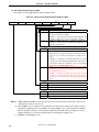
Renesas Electronics products are classified according to the following three quality grades: “Standard”, “High Quality”, and
“Specific”. The recommended applications for each Renesas Electronics product depends on the product’s quality grade, as
indicated below. You must check the quality grade of each Renesas Electronics product before using it in a particular
application. You may not use any Renesas Electronics product for any application categorized as “Specific” without the prior
written consent of Renesas Electronics. Further, you may not use any Renesas Electronics product for any application for
which it is not intended without the prior written consent of Renesas Electronics. Renesas Electronics shall not be in any way
liable for any damages or losses incurred by you or third parties arising from the use of any Renesas Electronics product for an
application categorized as “Specific” or for which the product is not intended where you have failed to obtain the prior written
consent of Renesas Electronics. The quality grade of each Renesas Electronics product is “Standard” unless otherwise
expressly specified in a Renesas Electronics data sheets or data books, etc.
“Standard”:
8.
9.
10.
11.
12.
Computers; office equipment; communications equipment; test and measurement equipment; audio and visual
equipment; home electronic appliances; machine tools; personal electronic equipment; and industrial robots.
“High Quality”: Transportation equipment (automobiles, trains, ships, etc.); traffic control systems; anti-disaster systems; anticrime systems; safety equipment; and medical equipment not specifically designed for life support.
“Specific”:
Aircraft; aerospace equipment; submersible repeaters; nuclear reactor control systems; medical equipment or
systems for life support (e.g. artificial life support devices or systems), surgical implantations, or healthcare
intervention (e.g. excision, etc.), and any other applications or purposes that pose a direct threat to human life.
You should use the Renesas Electronics products described in this document within the range specified by Renesas Electronics,
especially with respect to the maximum rating, operating supply voltage range, movement power voltage range, heat radiation
characteristics, installation and other product characteristics. Renesas Electronics shall have no liability for malfunctions or
damages arising out of the use of Renesas Electronics products beyond such specified ranges.
Although Renesas Electronics endeavors to improve the quality and reliability of its products, semiconductor products have
specific characteristics such as the occurrence of failure at a certain rate and malfunctions under certain use conditions. Further,
Renesas Electronics products are not subject to radiation resistance design. Please be sure to implement safety measures to
guard them against the possibility of physical injury, and injury or damage caused by fire in the event of the failure of a
Renesas Electronics product, such as safety design for hardware and software including but not limited to redundancy, fire
control and malfunction prevention, appropriate treatment for aging degradation or any other appropriate measures. Because
the evaluation of microcomputer software alone is very difficult, please evaluate the safety of the final products or system
manufactured by you.
Please contact a Renesas Electronics sales office for details as to environmental matters such as the environmental
compatibility of each Renesas Electronics product. Please use Renesas Electronics products in compliance with all applicable
laws and regulations that regulate the inclusion or use of controlled substances, including without limitation, the EU RoHS
Directive. Renesas Electronics assumes no liability for damages or losses occurring as a result of your noncompliance with
applicable laws and regulations.
This document may not be reproduced or duplicated, in any form, in whole or in part, without prior written consent of Renesas
Electronics.
Please contact a Renesas Electronics sales office if you have any questions regarding the information contained in this
document or Renesas Electronics products, or if you have any other inquiries.
(Note 1) “Renesas Electronics” as used in this document means Renesas Electronics Corporation and also includes its majorityowned subsidiaries.
(Note 2) “Renesas Electronics product(s)” means any product developed or manufactured by or for Renesas Electronics.
Application Note
78K0/Kx2-L
Sample Program (Low-Voltage Detection)
Reset Generation upon Detection of Voltage Less Than About 2.8 V
This document describes an operation overview of the sample program, as well as how to use the sample program and
how to set up and use the low-voltage detector. In the sample program, the low-voltage detector is used to detect that
VDD is less than VLVI (where VLVI is 2.84 ±0.1 V), and then generate an internal reset (LVI reset). By generating an LVI
reset, RAM data is retained and used to restore the LED lighting pattern immediately after the LVI reset ends to what it
was immediately before the LVI reset.
Target devices
78K0/KY2-L microcontroller
78K0/KA2-L microcontroller
78K0/KB2-L microcontroller
78K0/KC2-L microcontroller
Document No. U19696EJ1V0AN00 (1st edition)
Date Published September 2009 N
2009
Printed in Japan
CONTENTS
CHAPTER 1 OVERVIEW ...................................................................................3
1.1 Primary Initial Settings .............................................................................3
1.2 Processing After Main Loop.....................................................................4
1.3 Operation upon LVI Reset .......................................................................5
CHAPTER 2 CIRCUIT DIAGRAM ....................................................................6
2.1 Circuit Diagram ........................................................................................6
2.2 Used Devices Other than Microcontroller ................................................6
CHAPTER 3 SOFTWARE .................................................................................7
3.1 Included Files...........................................................................................7
3.2 Internal Peripheral Functions to Be Used ................................................8
3.3 Initial Settings and Operation Overview...................................................8
3.4 Flow Charts..............................................................................................9
CHAPTER 4 SETTING METHODS ................................................................11
4.1 Setting up Low-Voltage Detector ...........................................................11
4.2 Software Coding Example .....................................................................15
4.3 Setting up Startup Routine.....................................................................17
CHAPTER 5 RELATED DOCUMENTS..........................................................19
APPENDIX A PROGRAM LIST......................................................................20
APPENDIX B USING 78K0/KC2-L 44-PIN PRODUCTS .............................44
APPENDIX C REVISION HISTORY ...............................................................45
• The information in this document is current as of May, 2009. The information is subject to change
without notice. For actual design-in, refer to the latest publications of NEC Electronics data sheets,
etc., for the most up-to-date specifications of NEC Electronics products. Not all products and/or
types are available in every country. Please check with an NEC Electronics sales representative for
availability and additional information.
• No part of this document may be copied or reproduced in any form or by any means without the prior
written consent of NEC Electronics. NEC Electronics assumes no responsibility for any errors that may
appear in this document.
• NEC Electronics does not assume any liability for infringement of patents, copyrights or other intellectual
property rights of third parties by or arising from the use of NEC Electronics products listed in this document
or any other liability arising from the use of such products. No license, express, implied or otherwise, is
granted under any patents, copyrights or other intellectual property rights of NEC Electronics or others.
• Descriptions of circuits, software and other related information in this document are provided for illustrative
purposes in semiconductor product operation and application examples. The incorporation of these
circuits, software and information in the design of a customer's equipment shall be done under the full
responsibility of the customer. NEC Electronics assumes no responsibility for any losses incurred by
customers or third parties arising from the use of these circuits, software and information.
• While NEC Electronics endeavors to enhance the quality and safety of NEC Electronics products, customers
agree and acknowledge that the possibility of defects thereof cannot be eliminated entirely. In addition, NEC
Electronics products are not taken measures to prevent radioactive rays in the product design. When customers
use NEC Electronics products with their products, customers shall, on their own responsibility, incorporate
sufficient safety measures such as redundancy, fire-containment and anti-failure features to their products in
order to avoid risks of the damages to property (including public or social property) or injury (including death) to
persons, as the result of defects of NEC Electronics products.
• NEC Electronics products are classified into the following three quality grades: "Standard", "Special" and
"Specific".
The "Specific" quality grade applies only to NEC Electronics products developed based on a customerdesignated "quality assurance program" for a specific application. The recommended applications of an NEC
Electronics product depend on its quality grade, as indicated below. Customers must check the quality grade of
each NEC Electronics product before using it in a particular application.
"Standard": Computers, office equipment, communications equipment, test and measurement equipment, audio
and visual equipment, home electronic appliances, machine tools, personal electronic equipment
and industrial robots.
"Special": Transportation equipment (automobiles, trains, ships, etc.), traffic control systems, anti-disaster
systems, anti-crime systems, safety equipment and medical equipment (not specifically designed
for life support).
"Specific": Aircraft, aerospace equipment, submersible repeaters, nuclear reactor control systems, life
support systems and medical equipment for life support, etc.
The quality grade of NEC Electronics products is "Standard" unless otherwise expressly specified in NEC
Electronics data sheets or data books, etc. If customers wish to use NEC Electronics products in applications
not intended by NEC Electronics, they must contact an NEC Electronics sales representative in advance to
determine NEC Electronics' willingness to support a given application.
(Note)
(1) "NEC Electronics" as used in this statement means NEC Electronics Corporation and also includes its
majority-owned subsidiaries.
(2) "NEC Electronics products" means any product developed or manufactured by or for NEC Electronics (as
defined above).
M8E0904E
2
Application Note U19696EJ1V0AN
CHAPTER 1 OVERVIEW
In this sample program, an example of using the low-voltage detector is presented.
In the sample program, the low-voltage detector is specified to detect that VDD is less than VLVI (where VLVI is 2.84
±0.1 V), and then generate an internal reset (LVI reset).
After completion of the initial settings, an LED lighting pattern is displayed according to the number of switch inputs,
by detecting the falling edge of the switch input and performing interrupt servicing.
When a reset is generated by other than LVI, the program is used to initialize the number of switch inputs. When an
LVI reset is generated, the number of switch inputs immediately before reset generation is restored and an LED
lighting pattern is displayed accordingly immediately after the LVI reset ends, because RAM retains the data
immediately before the reset, unless it falls below the POC detection voltage (VPDR = 1.59 ±0.09 V)Note 1.
1.1
Primary Initial Settings
The primary initial settings are as follows:
<Option byte settings>
z Allowing the internal low-speed oscillator to be programmed to stop
z Disabling the watchdog timer
z Setting the internal high-speed oscillation clock frequency to 8 MHz
z Disabling LVI from being started by default
<Settings during initialization immediately after a reset ends>
z Specifying the ROM and RAM sizes
z Setting up I/O ports
z Setting up the low-voltage detectorNote 2
• Setting the LVI detection voltage (VLVI) to 2.84 ±0.1 V
• Specifying that an internal reset is generated if the supply voltage (VDD) is less than the LVI detection
voltage (VLVI)
z Specifying that the CPU clock runs on the internal high-speed oscillation clock (8 MHz)
z Stopping the internal low-speed oscillator
z Disabling peripheral hardware not to be used
z Outputting the LED lighting pattern
z Setting up INTP1 interrupts (by using the falling edge)
z Enabling interrupts
Notes 1. For details about the POC detection voltage, refer to the chapter about the power-on-clear circuit in the
78K0/Kx2-L User’s Manual.
2. Set up the low-voltage detector only if generating a reset other than an LVI reset.
Application Note U19696EJ1V0AN
3
CHAPTER 1 OVERVIEW
1.2
Processing After Main Loop
Interrupt servicing is performed by detecting the falling edge of the INTP1 pin, caused by switch input. In interrupt
servicing, the LED lighting pattern is changed by confirming that the switch is on, after about 10 ms have elapsed after
the falling edge of the INTP1 pin was detected. If the switch is off, after about 10 ms have elapsed, processing is
identified as chattering and the LED lighting pattern is not changed.
<Input>
<Output>
Switch turned on once
(kept on at least 10 ms)
LED1
LED2
LED3
78K0/Kx2-L
microcontroller
SW
Number of Switch
LED Lighting Pattern
Note
Inputs
LED1
LED2
LED3
0
Off
Off
Off
1
On
Off
Off
2
Off
On
Off
3
On
On
Off
4
Off
Off
On
5
On
Off
On
6
Off
On
On
7
On
On
On
Note The lighting patterns from the zeroth switch input are repeated after the eighth switch input.
Caution
For cautions when using the device, refer to the 78K0/Kx2-L User’s Manual.
[Column] Chattering
Chattering is a phenomenon in which the electric signal repeats turning on and off due to a mechanical
flip-flop of the contacts, immediately after the switch has been pressed.
4
Application Note U19696EJ1V0AN
CHAPTER 1 OVERVIEW
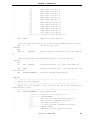
1.3
Operation upon LVI Reset
In this sample program, an internal reset (LVI reset) is generated by the low-voltage detector when VDD becomes
less than VLVI. At this time, RAM retains the data immediately before the reset, unless it falls below the POC detection
voltage (VPDR = 1.59 ±0.09 V)Note 1. The number of switch inputs immediately before the reset is retained until
immediately after the reset ends and an LED lighting pattern can therefore be displayed accordingly when an LVI reset
is generatedNote 2. When a reset is generated by other than LVI, the program is used to initialize the number of switch
inputs and all LEDs are turned off.
Figure 1-1. Overview of Operation upon LVI Reset
LVI reset
generation
<Output>
Switch turned on once
LVI reset
release
<Output>
Switch turned on once
Supply voltage (VDD)
LED1
LED2
LED3
LVI detection
voltage (VLVI)
POC detection
voltage (VPDR)
LED1
LED2
LED3
Notes 1. For details about the POC detection voltage, refer to the chapter about the power-on-clear circuit in the
78K0/Kx2-L User’s Manual.
2. As mentioned in [Column] below, when a standard startup routine is used in a C language program,
RAM data is initialized (cleared to 0) before the main function. To avoid this, a section of the standard
startup routine is commented out in this C language version sample program, so that RAM data without
initial values is not initialized.
[Column] Processing of the startup routine
A standard startup routine mainly performs the following processing.
• Stack pointer setting
• Hardware initialization (needed to be performed at an early stage)
• Initialization of variables to be used with a library
• Transferring from ROM to RAM the initial values of external variables with initial values, and sreg
variables
• Assigning 0 to RAM of external variables without initial values, and sreg variablesNote
Note
This processing is commented out in the source file (cstart.asm) of the startup routine included in
this C language version sample program.
For details, refer to the chapter regarding the startup routine of the CC78K0 C Compiler Operation
User’s Manual.
Application Note U19696EJ1V0AN
5
CHAPTER 2 CIRCUIT DIAGRAM
This chapter provides a circuit diagram and describes the devices used in this sample program other than the
microcontroller.
2.1
Circuit Diagram
A circuit diagram is shown below.
VDD
VDD
VDD
VDD
0.47 to 1 μ F
RESET
LED3
REGC
VSS
P60
78K0/Kx2-L
microcontroller
VDD
LED2
P01
VDD
LED1
SW
P00
INTP1/P30
Cautions 1. Use VDD in the following voltage range:
During normal operation:
2.94 V < VDD ≤ 5.5 V
When generating an LVI reset: 1.68 V < VDD ≤ 2.74 V
2. Connect the AVREF pin directly to VDD.
3. Connect the AVSS pin directly to GND (only for the 78K0/KC2-L and 78K0/KB2-L
microcontrollers).
4. Connect REGC to VSS via a capacitor (0.47 to 1 μF).
5. For the 78K0/KY2-L and 78K0/KA2-L, VSS is also used as the ground potential for the A/D
converter. Be sure to connect VSS to a stable GND.
6. Handle unused pins that are not shown in the circuit diagram as follows:
• I/O ports:
Set them to output mode and leave them open (unconnected).
• Input ports:
Connect them independently to VDD or VSS via a resistor.
7. In this sample program, the P121/X1/TOOLC0 and P122/X2/EXCLK/TOOLD0 pins are used for
on-chip debugging.
2.2
Used Devices Other than Microcontroller
The following devices are used in addition to the microcontroller:
(1) Switch (SW)
A switch is used as an input to control the lighting of an LED.
(2) LEDs (LED1, LED2, LED3)
The LEDs are used as outputs corresponding to switch inputs.
6
Application Note U19696EJ1V0AN
CHAPTER 3 SOFTWARE
This chapter describes the files included in the compressed file to be downloaded, internal peripheral functions of
the microcontroller to be used, and initial settings and provides an operation overview of the sample program and the
flow charts.
3.1
Included Files
The following table shows the files included in the compressed file to be downloaded.
(1) Assembly language version
File Name
main.asm
Description
Source file for hardware initialization processing and main processing
Compressed (*.zip) File Included
z
z
z
z
of microcontroller
op.asm
Assembler source file for setting the option byte
(This file is used for setting up the watchdog timer and internal lowspeed oscillator and selecting the internal high-speed oscillation clock
frequency.)
Kx2-L_LVI.prw
Work space file for integrated development environment PM+
z
Kx2-L_LVI.prj
Project file for integrated development environment PM+
z
(2) C language version
File Name
main.c
op.asm
Description
Compressed (*.zip) File Included
Source file for hardware initialization processing and main processing
of microcontroller
z
z
Assembler source file for setting the option byte
z
z
z
z
Library type setting file (include file of “cstart.asm”)
z
z
Macro definition file regarding various template patterns (include file of
z
z
(This file is used for setting up the watchdog timer and internal lowspeed oscillator and selecting the internal high-speed oscillation clock
frequency.)
cstart.asm
Startup routine source file (comments out a section of ROM
processing)
def.inc
macro.inc
“cstart.asm”)
Kx2-L_LVI.prw
Work space file for integrated development environment PM+
z
Kx2-L_LVI.prj
Project file for integrated development environment PM+
z
Remark
: Only the source files are included.
: The files to be used with integrated development environment PM+ are included.
Application Note U19696EJ1V0AN
7
CHAPTER 3 SOFTWARE
3.2
Internal Peripheral Functions to Be Used
The following internal peripheral functions of the microcontroller are used in this sample program.
• Low-voltage detector: Used to detect that VDD is less than VLVI and generate an LVI reset.
• INTP1:
Used for switch input.
• P00, P01, and P60:
Used to turn on or off three LEDs (LED1, LED2, and LED3).
3.3
Initial Settings and Operation Overview
In this sample program, the selection of the clock frequency, setting of the I/O ports, setting of interrupt, and setting
of the low-voltage detector are performed in the initial settings.
After completion of the initial settings, interrupt servicing is performed by detecting the falling edge of the switch
input (SW) and the lighting of the three LEDs (LED1, LED2, and LED3) is controlled according to the number of switch
inputs.
When a reset is generated by other than LVI, the program is used to initialize the number of switch inputs. When an
LVI reset is generated, the number of switch inputs immediately before reset generation is restored and an LED
lighting pattern is displayed accordingly immediately after the LVI reset ends, because RAM retains the data
immediately before the reset, unless it falls below the POC detection voltage (VPDR = 1.59 ±0.09 V).
The details are described in the state transition diagram shown below.
Initial settings 1
<Option byte settings>
z Allowing the internal low-speed oscillator to be programmed to stop
z Disabling the watchdog timer
z Setting the internal high-speed oscillation clock frequency to 8 MHz
z Disabling LVI from being started by default
<Settings during initialization immediately after a reset ends>
z Specifying the ROM and RAM sizes
z Setting up I/O ports
• Specifying P00, P01, and P60 as pins used to output signals to the LEDs
• Specifying P30/INTP1 as a switch input pin
LVI reset
Settings when generating a reset other than LVI reset
z Setting up the low-voltage detector
• Setting the LVI detection voltage (VLVI) to 2.84 ±0.1 V
• Specifying that an internal reset is generated if the
supply voltage (VDD) is less than the LVI detection
voltage (VLVI)
Reset other than
LVI reset
Reset source check
Make the system wait until VDD ≥ VLVI.
VDD ≥ VLVI
Initial settings 2
z Specifying that the CPU clock runs on the internal high-speed oscillation
clock (8 MHz)
z Stopping the internal low-speed oscillator
z Disabling peripheral hardware not to be used
z Outputting the LED lighting pattern (RAM) to P00, P01, and P60
z Setting up INTP1 interrupts (by using the falling edge)
z Enabling interrupts
Make the system wait for switch input.
INTP1 falling edge
detection
Chattering
detection
Make the system wait for about
10 ms to prevent chattering.
8
Switch input
detection
Initialize the LED lighting pattern
(RAM). (Turn off all LEDs.)
LED lighting pattern
No. of SW Inputs
LED1
LED2
LED3
0
Off
Off
Off
1
On
Off
Off
2
Off
On
Off
3
On
On
Off
4
Off
Off
On
5
On
Off
On
6
Off
On
On
7
On
On
On
* The lighting patterns from the zeroth switch input
are repeated after the eighth switch input.
Application Note U19696EJ1V0AN
CHAPTER 3 SOFTWARE
3.4
Flow Charts
The flow charts for the sample program are shown below.
<Initialization immediately after a reset ends>
Start
1
The option byte is
Note 1
referenced.
Output the LED lighting
pattern (RAM) to P00, P01,
and P60.
Disable interrupts.
Set up the register bank.
Set up INTP1 interrupts
(by using the falling edge).
Specify the ROM and RAM sizes.
Enable interrupts.
Specify the stack pointer.
Main loop
Set up I/O ports.
No
Is the
reset source other than
Note 2
LVI?
Yes
Disable the INTLVI interrupt.
Specify the supply voltage
(VDD) as the low-voltage
detector detection voltage.
Set the low-voltage detection
level of the low-voltage
detector (VLVI) to 2.84 ±0.1 V.
Note 3
Enable low-voltage detection.
No
VDD ≥ VLVI?
Yes
Specify the low-voltage
detector to generate an
internal reset when VDD falls
below VLVI.
Initialize the LED lighting
pattern (RAM).
(Turn off all LEDs.)
Specify that the CPU clock
runs on the internal highspeed oscillation clock
(8 MHz).
Stop the internal low-speed
oscillator.
<INTP1 interrupt servicing>
Start
Initial
settings for
the lowvoltage
detector
Switch the register bank.
Initialization
No
Have 10
ms elapsed after falling
edge detection?
Yes
Clear the INTP1 interrupt request.
No
Has
switch input been
detected?
Yes
Switch the number of switch
inputs according to the LED
lighting pattern (RAM).
Output the LED lighting
pattern (RAM) to P00, P01,
and P60.
Disable peripheral hardware
not to be used.
Return
1
Application Note U19696EJ1V0AN
9
CHAPTER 3 SOFTWARE
Notes 1. The option byte is automatically referenced by the microcontroller immediately after a reset ends. In this
sample program, the following settings are specified using the option byte:
• Allowing the internal low-speed oscillator to be programmed to stop
• Disabling the watchdog timer
• Setting the internal high-speed oscillation clock frequency to 8 MHz
• Disabling LVI from being started by default
2. Use the reset control flag register (RESF) to check the reset source. For details about RESF, refer to the
chapter about the reset function in the 78K0/Kx2-L User’s Manual.
3. The low-voltage detector is enabled, and then the system is made to wait at least 10 μs until the lowvoltage detector stabilizes.
10
Application Note U19696EJ1V0AN
CHAPTER 4 SETTING METHODS
This chapter describes how to set up the low-voltage detector and the startup routine and provides a software
coding example.
For other initial settings, refer to the 78K0/Kx2-L Sample Program (Initial Settings) LED Lighting Switch Control
Application Note.
For how to set registers, refer to the 78K0/Kx2-L User’s Manual.
For assembler instructions, refer to the 78K/0 Series Instructions User’s Manual.
4.1
Setting up Low-Voltage Detector
The low-voltage detector is mainly controlled by the following two types of registers:
• Low-voltage detection register (LVIM)
• Low-voltage detection level select register (LVIS)
[Example of the setup procedure when using the low-voltage detector to generate a reset]
(The same procedure is used in the sample program.)
<1> Mask LVI interrupts (LVIMK = 1).
<2> Clear bit 2 (LVISEL) of the low-voltage detection register (LVIM) to 0 (to detect the supply voltage (VDD)
level).
<3> Specify the LVI detection voltage by using bits 3 to 0 (LVIS3 to LVIS0) of the low-voltage detection level
select register (LVIS).
<4> Set bit 7 (LVION) of LVIM to 1 (to enable LVI).
<5> Program the system to wait for the operation stabilization time (about 10 μs).
<6> Make the system wait until the supply voltage (VDD) is confirmed to be equal to or greater than the LVI
detection voltage (VLVI) by using bit 0 (LVIF) of LVIM.
<7> Set bit 1 (LVIMD) of LVIM to 1 (to generate a reset when the specified level is detected).
Cautions 1. This is the setup procedure when LVI is disabled to start by default (LVISTART = 0) by using
the option byte.
2. Be sure to perform step <1>. If LVIMK is 0, an interrupt might be generated after step <4> is
performed.
3. No internal reset signal is generated if the supply voltage (VDD) is equal to or greater than the
LVI detection voltage (VLVI) when LVIMD has been set to 1.
Application Note U19696EJ1V0AN
11
CHAPTER 4 SETTING METHODS
(1) Low-voltage detection register (LVIM)
This register sets low-voltage detection and the operation mode.
Figure 4-1. Format of Low-Voltage Detection Register (LVIM)
LVION
0
0
0
0
Note 3
LVISEL
LVIMD
LVIF
LVIF
Low-voltage detection flag
0
• LVISEL = 0: Supply voltage (VDD) ≥ LVI detection voltage (VLVI),
or when LVI operation is disabled
• LVISEL = 1: Input voltage from external input pin (EXLVI) ≥ LVI
detection voltage (VEXLVI), or when LVI operation is disabled
• LVISEL = 0: Supply voltage (VDD) < LVI detection voltage (VLVI)
1
• LVISEL = 1: Input voltage from external input pin (EXLVI) < LVI
detection voltage (VEXLVI)
Note 1
LVIMD
0
Low-voltage detection operation mode (interrupt/reset) selection
• LVISEL = 0: Generates an internal interrupt signal when the
supply voltage (VDD) drops lower than the LVI detection voltage
(VLVI) (VDD < VLVI) or when VDD becomes VLVI or higher (VDD ≥
VLVI).
• LVISEL = 1: Generates an interrupt signal when the input
voltage from an external input pin (EXLVI) drops lower than the
LVI detection voltage (VEXLVI) (EXLVI < VEXLVI) or when EXLVI
becomes VEXLVI or higher (EXLVI ≥ VEXLVI).
1
• LVISEL = 0: Generates an internal reset signal when the supply
voltage (VDD) < the LVI detection voltage (VLVI) and releases the
reset signal when VDD ≥ VLVI.
• LVISEL = 1: Generates an internal reset signal when the input
voltage from an external input pin (EXLVI) < the LVI detection
voltage (VEXLVI) and releases the reset signal when EXLVI ≥
VEXLVI.
LVISEL
Notes 1, 3
Voltage detection selection
0
Detects level of supply voltage (VDD)
1
Detects level of input voltage from external input pin (EXLVI)
LVION
Notes 1, 2
Enables low-voltage detection operation
0
Disables operation
1
Enables operation
Notes 1. LVION, LVIMD, and LVISEL are cleared to 0 in the case of a reset other than an LVI reset. These are not
cleared to 0 in the case of an LVI reset.
2. When LVION is set to 1, operation of the comparator in the LVI circuit is started. Use software to wait for
an operation stabilization time (10 μs (MAX.)) from when LVION is set to 1 until operation is stabilized.
After the operation stabilizes, an external input (minimum pulse width: 200 μs) of 200 μs or more is
required until LVIF is set (1) after the voltage drops to the LVI detection voltage or less.
3. 78K0/KB2-L and 78K0/KC2-L only.
12
Application Note U19696EJ1V0AN
CHAPTER 4 SETTING METHODS
Cautions 1. To stop LVI, follow either of the procedures below.
• When using 8-bit memory manipulation instruction: Write 00H to LVIM.
• When using 1-bit memory manipulation instruction: Clear LVION to 0.
2. Input voltage from external input pin (EXLVI) must be EXLVI < VDD.
3. If LVI operation is disabled (clears LVION) when LVI is used in interrupt mode (LVIMD = 0),
LVISEL is set to 0, and the supply voltage (VDD) is less than or equal to the detection voltage
(VLVI), or when LVI is used in interrupt mode (LVIMD = 0), LVISEL is set to 1, and input voltage
of external input pin (EXLVI) is less than or equal to the detection voltage (VEXLVI)), an interrupt
request signal (INTLVI) is generated and LVIIF may be set to 1.
4. Be sure to clear the following bits to 0:
• 78K0/KY2-L, 78K0/KA2-L: Bits 6 to 2
• 78K0/KB2-L, 78K0/KC2-L: Bits 6 to 3
5. The LVIM reset value varies depending on the reset source and option byte setting and is as
follows:
• For an LVI reset:
The value specified before the reset is retained.
• For a reset other than an LVI reset:
(a) If the LVISTART option byte is 1: 82H
(b) If the LVISTART option byte is 0: 00H
6. Bit 0 is read-only.
Remark
The values written in red in the above figure are specified in this sample program.
Application Note U19696EJ1V0AN
13
CHAPTER 4 SETTING METHODS
(2) Low-voltage detection level select register (LVIS)
This register selects the low-voltage detection level.
Figure 4-2. Format of Low-Voltage Detection Level Select Register (LVIS)
0
0
0
0
LVIS3
LVIS2
LVIS1
LVIS0
LVIS3
LVIS2
LVIS1
LVIS0
0
0
0
0
VLVI0 (4.22 ±0.1 V)Note
Detection level
0
0
0
1
VLVI1 (4.07 ±0.1 V)Note
0
0
1
0
VLVI2 (3.92 ±0.1 V)Note
0
0
1
1
VLVI3 (3.76 ±0.1 V)Note
0
1
0
0
VLVI4 (3.61 ±0.1 V)Note
0
1
0
1
VLVI5 (3.45 ±0.1 V)Note
0
1
1
0
VLVI6 (3.30 ±0.1 V)Note
0
1
1
1
VLVI7 (3.15 ±0.1 V)Note
1
0
0
0
VLVI8 (2.99 ±0.1 V)Note
1
0
0
1
VLVI9 (2.84 ±0.1 V)Note
1
0
1
0
VLVI10 (2.68 ±0.1 V)Note
1
0
1
1
VLVI11 (2.53 ±0.1 V)Note
1
1
0
0
VLVI12 (2.38 ±0.1 V)Note
1
1
0
1
VLVI13 (2.22 ±0.1 V)Note
1
1
1
0
VLVI14 (2.07 ±0.07 V)Note
1
1
1
1
VLVI15 (1.91 ±0.1 V)Note
Note These are preliminary values and subject to change.
Cautions 1. Be sure to clear bits 7 to 4 to “0”.
2. Do not change the value of LVIS during LVI operation.
3. When an input voltage from the external input pin (EXLVI) is detected, the LVI detection
voltage (VEXLVI = 1.21 V (TYP.)) is fixed. Therefore, setting of LVIS is not necessary.
4. The LVIS reset value varies depending on the reset source and option byte setting and is as
follows:
• For an LVI reset:
The value specified before the reset is retained.
• For a reset other than an LVI reset:
(a) If the LVISTART option byte is 1: 0FH
(b) If the LVISTART option byte is 0: 00H
Remark
14
The values written in red in the above figure are specified in this sample program.
Application Note U19696EJ1V0AN
CHAPTER 4 SETTING METHODS
4.2 Software Coding Example
The settings to be specified for the low-voltage detector in the 78K0/KC2-L sample program are shown below as a
software coding example.
(1) Assembly language
XMAIN CSEG
UNIT
RESET_START:
Mask LVI interrupts.
...(Omitted)...
SET1
LVIMK
MOV
LVIM,
...(Omitted)...
MOV
LVIS,
Specify the supply voltage
(VDD) as the detection voltage.
#00000000B
; Disable the INTVLI interrupt
; Low-voltage detection register
Set the LVI detection voltage to 2.84 ±0.1 V.
#00001001B
; Low-voltage detection level select register
...(Omitted)...
SET1
LVION
; Enable low-voltage detection
Enable low-voltage
detection.
; Make the system wait until the low-voltage detector stabilizes (10 us
or more)
MOV
B,
#5
; Specify the count value
The system waits at
HRES100:
least 10 μs.
NOP
DBNZ
B,
$HRES100
; Has the operation stabilization wait time
elapsed? No,
; Make the system wait until VDD becomes equal to or greater than VLVI
HRES110:
The system waits until VDD ≥ VLVI.
NOP
BT
LVIF, $HRES110
; Has VDD become equal to or greater than VLVI?
No,
Specify a reset to be generated when VDD < VLVI.
SET1
LVIMD
; Specify an internal reset to be generated
when VDD falls below VLVI
Application Note U19696EJ1V0AN
15
CHAPTER 4 SETTING METHODS
(2) C language
void hdwinit(void)
{
Specify the supply voltage
Mask LVI interrupts.
(VDD) as the detection voltage.
...(Omitted)...
LVIMK = 1;
/* Disable the INTVLI interrupt */
LVIM
= 0b00000000; /* Low-voltage detection register */
...(Omitted)...
Set the LVI detection voltage to 2.84 ±0.1 V.
LVIS
= 0b00001001; /* Low-voltage detection level select register */
...(Omitted)...
LVION
= 1;
Enable low-voltage detection.
/* Enable low-voltage detection */
/* Make the system wait until the low-voltage detector stabilizes (10 us
or more) */
The system waits
for ( ucCounter = 0; ucCounter < 2; ucCounter++){
at least 10 μs.
NOP();
}
/* Make the system wait until VDD becomes equal to or greater than VLVI
*/
while( LVIF ){
NOP();
}
LVIMD = 1;
below VLVI */
Remark
The system waits
until VDD ≥ VLVI.
Specify a reset to be
generated when VDD < VLVI.
/* Specify an internal reset to be generated when VDD falls
In this sample program, fCPU (the CPU clock frequency) is 4 MHz when the low-voltage detector is set
up. Therefore, the wait time above (10 μs) is calculated based on fCPU being 4 MHz.
16
Application Note U19696EJ1V0AN
CHAPTER 4 SETTING METHODS
4.3 Setting up Startup Routine
In the C language version of this sample program, a startup routine defined for this sample program is used instead
of a standard startup routine. To use a user-defined startup routine, that startup routine must be set up using PM+.
How to set up the startup routine used in the C language version of this sample program is described below.
For details about how to use PM+, refer to the PM+ Project Manager User’s Manual. For details about startup
routines, refer to the chapter about startup routines in the CC78K0 C Compiler Operation User’s Manual.
(1) Setting up source files
In the C language version of this sample program, the startup routine source file “cstart.asm”, library type
specification file “def.inc”, and macro definition file “macro.inc” are used in addition to “main.c” and “op.asm”.
Open the [Project] menu in PM+ and select [Project Settings]. The Project Settings dialog box opens. In this
dialog box, select “main.c”, “op.asm”, and “cstart.asm” as the source files.
Click [Add] to select “main.c”,
“op.asm”, and “cstart.asm”.
Click [OK] after “main.c”,
“op.asm”, and “cstart.asm” have
been added as source files.
“main.c”, “op.asm”, “cstart.asm”,
“def.inc”, and “macro.inc” are
added to the project.
Application Note U19696EJ1V0AN
17
CHAPTER 4 SETTING METHODS
(2) Specifying compiler options
Open the [Tool] menu in PM+ and select [Compiler Options]. The Compiler Options dialog box opens. In this
dialog box, deselect the [Using Startup Routine] checkbox.
Deselect.
(3) Specifying linker options
Open the [Tool] menu in PM+ and select [Linker Options]. The Linker Options dialog box opens. In this dialog
box, select the [Create Stack Symbol [-s]] checkbox.
Select.
18
Application Note U19696EJ1V0AN
CHAPTER 5 RELATED DOCUMENTS
The related documents indicated in this publication may include preliminary versions.
However, preliminary
versions are not marked as such.
Document Name
English
78K0/Kx2-L User’s Manual
PDF
78K/0 Series Instructions User’s Manual
PDF
RA78K0 Assembler Package User’s Manual
CC78K0 C Compiler User’s Manual
Language
PDF
Operation
PDF
Language
PDF
Operation
PDF
PM+ Project Manager User’s Manual
PDF
78K0/Kx2-L
PDF
Sample Program (Initial Settings) LED Lighting Switch Control
Application Note
Application Note U19696EJ1V0AN
19
APPENDIX A PROGRAM LIST
As a program list example, the 78K0/KC2-L microcontroller source program is shown below.
z main.asm (assembly language version)
;*******************************************************************************
;
;
NEC Electronics
78K0/KC2-L Series
;
;*******************************************************************************
;
78K0/KC2-L Series
Sample Program (Low-Voltage Detection)
;*******************************************************************************
;
Reset Generation upon Detection of Voltage Less Than About 2.8 V
;*******************************************************************************
;<<History>>
;
2009.1.--
Release
;*******************************************************************************
;
;<<Overview>>
;
; This sample program presents an example of using the low-voltage detector.
; In the sample program, the low-voltage detector is specified to detect that VDD is
; less than VLVI (where VLVI is 2.84 ±0.1 V), and then generate an internal reset
; (LVI reset).
After completion of the initial settings, an LED lighting pattern is
; displayed according to the number of switch inputs, by detecting the falling edge
; of the switch input and performing interrupt servicing.
When a reset is generated
; by other than LVI, the program is used to initialize the number of switch inputs.
; When an LVI reset is generated, the number of switch inputs immediately before
; reset generation is restored and an LED lighting pattern is displayed accordingly
; immediately after the LVI reset ends, because RAM retains the data immediately
; before the reset, unless it falls below the POC detection voltage (VPDR = 1.59
; ±0.09 V).
;
;
; <Primary initial settings>
; (Option byte settings)
; - Allowing the internal low-speed oscillator to be programmed to stop
; - Disabling the watchdog timer
; - Setting the internal high-speed oscillation clock frequency to 8 MHz
; - Disabling LVI from being started by default
; (Settings during initialization immediately after a reset ends)
; - Specifying the ROM and RAM sizes
; - Setting up I/O ports
; - Setting up the low-voltage detector
;
→ Setting the LVI detection voltage (VLVI) to 2.84 ±0.1 V
;
→ Specifying that an internal reset is generated if the supply voltage (VDD) is
less than the LVI detection voltage (VLVI)
20
Application Note U19696EJ1V0AN
APPENDIX A PROGRAM LIST
; - Specifying that the CPU clock runs on the internal high-speed oscillation clock
(8 MHz)
; - Stopping the internal low-speed oscillator
; - Disabling peripheral hardware not to be used
; - Outputting the LED lighting pattern
; - Setting up INTP1 interrupts (by using the falling edge)
; - Enabling interrupts
;
;
; <LED lighting pattern immediately after the reset ends>
;
; - Reset generated by other than the low-voltage detector:
Turn off all LEDs
; - Reset generated by the low-voltage detector:
Retain
the
LED
lighting pattern before the reset
;
;
; <Number of switch inputs and LED lighting patterns>
;
; +---------------------------------------+
; | SW Inputs
| LED1
; | (P30/INTP1)
| (P00) | (P01) | (P60) |
| LED2
| LED3
|
; |---------------|-----------------------|
; | 0 times
| Off
| Off
| Off
|
; | 1 time
| On
| Off
| Off
|
; | 2 times
| Off
| On
| Off
|
; | 3 times
| On
| On
| Off
|
; | 4 times
| Off
| Off
| On
|
; | 5 times
| On
| Off
| On
|
; | 6 times
| Off
| On
| On
|
; | 7 times
| On
| On
| On
|
; +---------------------------------------+
; * The lighting patterns from the zeroth switch input are repeated after the eighth
switch input.
; * If the switch is turned on, 0 is input to the ports.
If the switch is turned off,
1 is input to the ports.
; * The LEDs turn off if 1 is output from the ports and turn on if 0 is output from
the ports.
;
;
; <I/O port settings>
;
Output: P00, P01, P60
;
Input:
;
* Set all unused ports that can be specified as output ports as output ports.
P30
;
;*******************************************************************************
;===============================================================================
Application Note U19696EJ1V0AN
21
APPENDIX A PROGRAM LIST
;
;
Vector table
;
;===============================================================================
XVECT1
DW
CSEG
AT
RESET_START
XVECT2
CSEG
0000H
;0000H RESET input, POC, LVI, WDT
AT
0004H
DW
IINIT
;0004H INTLVI
DW
IINIT
;0006H INTP0
DW
IINT_P1
;0008H INTP1
DW
IINIT
;000AH INTP2
DW
IINIT
;000CH INTP3
DW
IINIT
;000EH INTP4
DW
IINIT
;0010H INTP5
DW
IINIT
;0012H INTSRE6
DW
IINIT
;0014H INTSR6
DW
IINIT
;0016H INTST6
DW
IINIT
;0018H INTCSI10
DW
IINIT
;001AH INTTMH1
DW
IINIT
;001CH INTTMH0
DW
IINIT
;001EH INTTM50
DW
IINIT
;0020H INTTM000
DW
IINIT
;0022H INTTM010
DW
IINIT
;0024H INTAD
DW
IINIT
;0026H INTP6
DW
IINIT
;0028H INTRTCI
DW
IINIT
;002AH INTTM51
DW
IINIT
;002CH INTKR
DW
IINIT
;002EH INTRTC
DW
IINIT
;0030H INTP7
DW
IINIT
;0032H INTP8
DW
IINIT
;0034H INTIICA0
DW
IINIT
;0036H INTCSI11
DW
IINIT
;0038H INTP9
DW
IINIT
;003AH INTP10
DW
IINIT
;003CH INTP11
DW
IINIT
;003EH BRK
;===============================================================================
;
;
Define the RAM data table
;
;===============================================================================
DLED DSEG
SADDR
RLEDBUF:
DS
1
; Area in which to save the LED lighting pattern
;===============================================================================
22
Application Note U19696EJ1V0AN
APPENDIX A PROGRAM LIST
;
;
Define the memory stack area
;
;===============================================================================
DSTK DSEG
IHRAM
STACKEND:
DS
20H
; Memory stack area = 32 bytes
STACKTOP:
; Start address of the memory stack area
;*******************************************************************************
;
;
Servicing interrupts by using unnecessary interrupt sources
;
;*******************************************************************************
XMAIN
CSEG
UNIT
IINIT:
;
If an unnecessary interrupt occurred, the processing branches to this line.
;
The
processing
then
returns
to
the
initial
original
processing
because
no
processing is performed here.
RETI
;*******************************************************************************
;
;
Initialization after RESET
;
;*******************************************************************************
RESET_START:
;------------------------------------------------------------------------------;
Disable interrupts
;------------------------------------------------------------------------------DI
; Disable interrupts
;------------------------------------------------------------------------------;
Set up the register bank
;------------------------------------------------------------------------------SEL
RB0
; Set up the register bank
;------------------------------------------------------------------------------;
Specify the ROM and RAM sizes
;------------------------------------------------------------------------------;
Note that the values to specify vary depending on the model.
;
Enable the settings for the model to use. (The uPD78F0588 is the default model.)
;------------------------------------------------------------------------------; Setting when using uPD78F0581 or uPD78F0586
;MOV
IMS,
#042H
; Specify the ROM and RAM sizes
Application Note U19696EJ1V0AN
23
APPENDIX A PROGRAM LIST
; Setting when using uPD78F0582 or uPD78F0587
;MOV
IMS,
#004H
; Specify the ROM and RAM sizes
; Setting when using uPD78F0583 or uPD78F0588
MOV
IMS,
#0C8H
; Specify the ROM and RAM sizes
;------------------------------------------------------------------------------;
Initialize the stack pointer
;------------------------------------------------------------------------------MOVW
SP,
#STACKTOP
; Initialize the stack pointer
;------------------------------------------------------------------------------;
Initialize port 0
;------------------------------------------------------------------------------MOV
P0,
#00000011B
; Set the P00 and P01 output latches to high level
; Set the P02 output latch to low level
MOV
PM0,
#11111000B
; Specify P00 to P02 as output ports
; P00: Use to output a signal to LED1
; P01: Use to output a signal to LED2
; P02: Unused
;------------------------------------------------------------------------------;
Initialize port 1
;------------------------------------------------------------------------------MOV
ADPC1, #00000111B
; Specify P10 to P12 as digital I/O ports
MOV
P1,
#00000000B
; Set the P10 to P17 output latches to low level
MOV
PM1,
#00000000B
; Specify P10 to P17 as output ports
; P10 to P17: Unused
;------------------------------------------------------------------------------;
Initialize port 2
;------------------------------------------------------------------------------MOV
ADPC0, #11111111B
; Specify P20 to P27 as digital I/O ports
MOV
P2,
#00000000B
; Set the P20 to P27 output latches to low level
MOV
PM2,
#00000000B
; Specify P20 to P27 as output ports
; P20 to P27: Unused
;------------------------------------------------------------------------------;
Initialize port 3
;------------------------------------------------------------------------------MOV
P3,
#00000000B
; Set the P30 to P33 output latches to low level
MOV
PM3,
#11110001B
; Specify P30 as an input port
MOV
PU3,
#00000001B
; Specify P31 to P33 as output ports
; Connect an internal pull-up resistor to P30
; Do not connect internal pull-up resistors to P31 to
P33
; P30: Use as a switch input pin (INTP1)
24
Application Note U19696EJ1V0AN
APPENDIX A PROGRAM LIST
; P31 to P33: Unused
;------------------------------------------------------------------------------;
Initialize port 4
;------------------------------------------------------------------------------MOV
P4,
#00000000B
MOV
PM4,
#11111000B
; Set the P40 to P42 output latches to low level
; Specify P40 to P42 as output ports
; P40 to P42: Unused
;------------------------------------------------------------------------------;
Initialize port 6
;------------------------------------------------------------------------------MOV
P6,
#00000001B
MOV
PM6,
#11110000B
; Set the P60 output latch to high level
; Set the P61 to P63 output latches to low level
; Specify P60 to P63 as output ports
; P60: Use to output a signal to LED3
; P61 to P63: Unused
;------------------------------------------------------------------------------;
Initialize port 7
;------------------------------------------------------------------------------MOV
P7,
#00000000B
; Set the P70 to P75 output latches to low level
MOV
PM7,
#11000000B
; Specify P70 to P75 as output ports
; P70 to P75: Unused
;------------------------------------------------------------------------------;
Initialize port 12
;------------------------------------------------------------------------------MOV
P12,
#00000000B
MOV
PM12,
#11111110B
; Set the P120 output latch to low level
; Specify P120 as an output port
; P120 to P125: Unused
;------------------------------------------------------------------------------;
Set up the low-voltage detector
;------------------------------------------------------------------------------; Check the reset source (Omit this setting for a reset generated by the lowvoltage detector)
MOV
A,
RESF
; Read the reset source
BT
A.0,
$HRES120
;
Has
a
reset
been
generated
by
the
low-voltage
detector? Yes,
; Set up the low-voltage detector
SET1
LVIMK
MOV
LVIM,
; Disable the INTVLI interrupt
#00000000B
; Low-voltage detection register
;
|||||||+------- LVIF
;
|||||||
;
|||||||
;
|||||||
[Low-voltage detection flag]
0: - LVISEL = 0: Supply voltage (VDD) >= LVI
detection voltage (VLVI), or when LVI
Application Note U19696EJ1V0AN
25
APPENDIX A PROGRAM LIST
;
|||||||
;
|||||||
operation is disabled
;
|||||||
;
|||||||
;
|||||||
;
|||||||
;
|||||||
- LVISEL = 1: Input voltage from external input
;
|||||||
pin (EXLVI) < LVI detection voltage (VEXLVI)
;
||||||+-------- LVIMD
;
||||||
- LVISEL = 1: Input voltage from external input
pin (EXLVI) >= LVI detection voltage
(VEXLVI), or when LVI operation is disabled
1: - LVISEL = 0: Supply voltage (VDD) < LVI
detection voltage (VLVI)
[Low-voltage
detection
operation
mode
(interrupt/reset) selection]
;
||||||
0: - LVISEL = 0: Generate an internal interrupt
;
||||||
signal when the supply voltage (VDD) drops
;
||||||
lower than the LVI detection voltage (VLVI)
;
||||||
(VDD < VLVI) or when VDD becomes VLVI or
;
||||||
;
||||||
- LVISEL = 1: Generate an interrupt signal when
;
||||||
the input voltage from an external input pin
;
||||||
(EXLVI) drops lower than the LVI detection
;
||||||
voltage (VEXLVI) (EXLVI < VEXLVI) or when
;
||||||
EXLVI becomes VEXLVI or higher (EXLVI >=
;
||||||
;
||||||
1: - LVISEL = 0: Generate an internal reset signal
;
||||||
when the supply voltage (VDD) < the LVI
;
||||||
detection voltage (VLVI) and releases the
;
||||||
;
||||||
- LVISEL = 1: Generate an internal reset signal
;
||||||
when the input voltage from an external input
;
||||||
pin (EXLVI) < the LVI detection voltage
;
||||||
(VEXLVI) and releases the reset signal when
;
||||||
EXLVI >= VEXLVI
;
|||||+--------- LVISEL
;
|||||
;
|||||
0: Detect level of supply voltage (VDD)
;
|||||
1: Detect level of input voltage from external
;
|||||
;
|++++---------- Be sure to clear this bit to 0
;
+-------------- LVION
;
higher (VDD >= VLVI)
VEXLVI)
reset signal when VDD >= VLVI
[Voltage detection selection]
input pin (EXLVI)
[Enable low-voltage detection operation]
;
0: Disable operation
;
1: Enable operation
MOV
LVIS,
#00001001B
; Low-voltage detection level select register
;
||||++++------- LVIS3 to LVIS0
;
||||
0000: VLVI0 (4.22 ±0.1 V)
;
||||
0001: VLVI1 (4.07 ±0.1 V)
;
||||
0010: VLVI2 (3.92 ±0.1 V)
;
||||
0011: VLVI3 (3.76 ±0.1 V)
26
Application Note U19696EJ1V0AN
APPENDIX A PROGRAM LIST
;
||||
0100: VLVI4 (3.61 ±0.1 V)
;
||||
0101: VLVI5 (3.45 ±0.1 V)
;
||||
0110: VLVI6 (3.30 ±0.1 V)
;
||||
0111: VLVI7 (3.15 ±0.1 V)
;
||||
1000: VLVI8 (2.99 ±0.1 V)
;
||||
1001: VLVI9 (2.84 ±0.1 V)
;
||||
1010: VLVI10 (2.68 ±0.1 V)
;
||||
1011: VLVI11 (2.53 ±0.1 V)
;
||||
1100: VLVI12 (2.38 ±0.1 V)
;
||||
1101: VLVI13 (2.22 ±0.1 V)
;
||||
1110: VLVI14 (2.07 ±0.1 V)
;
||||
1111: VLVI15 (1.91 ±0.1 V)
;
++++----------- Be sure to clear this bit to 0
SET1
LVION
; Enable low-voltage detection
; Make the system wait until the low-voltage detector stabilizes (10 us or more)
MOV
B,
#5
; Specify the count value
B,
$HRES100
; Has the operation stabilization wait time elapsed?
HRES100:
NOP
DBNZ
No,
; Make the system wait until VDD becomes equal to or greater than VLVI
HRES110:
NOP
BT
LVIF,
SET1
LVIMD
$HRES110
; Has VDD become equal to or greater than VLVI? No,
; Specify an internal reset to be generated when VDD
falls below VLVI
MOV
RLEDBUF,#00000111B
; Initialize the LED lighting pattern
HRES120:
;------------------------------------------------------------------------------;
Specify the clock frequency
;------------------------------------------------------------------------------;
Specify the clock frequency so that the device can run on the internal high-
speed oscillation clock.
;------------------------------------------------------------------------------MOV
OSCCTL,#00000000B
; Clock operation mode
;
||||+||+------- Be sure to clear this bit to 0
;
|||| ++-------- RSWOSC/AMPHXT
;
||||
;
||||
00: Low power consumption oscillation
;
||||
01: Normal oscillation
;
||||
1x: Ultra-low power consumption oscillation
;
||++----------- EXCLKS/OSCSELS
;
||
[XT1 oscillator oscillation mode selection]
[Subsystem clock pin operation setting]
Application Note U19696EJ1V0AN
27
APPENDIX A PROGRAM LIST
;
||
;
||
(P123/XT1,P124/XT2/EXCLKS)
Specify the use of the pin as an I/O port pin by
specifying 000 by also using XTSTART
;
++------------- EXCLK/OSCSEL
;
[High-speed system clock pin operation setting]
;
(P121/X1,P122/X2/EXCLK)
;
00: Input port
;
01: X1 oscillation mode
;
10: Input port
;
11: External clock input mode
MOV
PCC,
#00000000B
; Select the CPU clock (fCPU)
;
|||+|+++------- CSS/PCC2/PCC1/PCC0
;
||| |
;
||| |
0000:fXP
;
||| |
0001:fXP/2
;
||| |
0010:fXP/2^2
;
||| |
0011:fXP/2^3
;
||| |
0100:fXP/2^4
;
||| |
1000:fSUB/2
;
||| |
1001:fSUB/2
;
||| |
1010:fSUB/2
;
||| |
1011:fSUB/2
;
||| |
1100:fSUB/2
;
||| |
(Other than the above: Setting prohibited)
[CPU clock (fCPU) selection]
;
||| +---------- Be sure to clear this bit to 0
;
||+------------ CLS
;
||
;
|+------------- XTSTART
[CPU clock status]
;
|
;
|
[Subsystem clock pin operation setting]
Specify the use of the pin by also using EXCLKS
and OSCSELS
;
+-------------- Be sure to clear this bit to 0
MOV
RCM,
#00000010B
;
Select
the
operating
mode
of
the
internal
oscillator
;
|||||||+------- RSTOP
;
|||||||
;
|||||||
0: Internal high-speed oscillator oscillating
;
|||||||
1: Internal high-speed oscillator stopped
;
||||||+-------- LSRSTOP
;
||||||
;
||||||
0: Internal low-speed oscillator oscillating
;
||||||
1: Internal low-speed oscillator stopped
;
|+++++--------- Be sure to clear this bit to 0
;
+-------------- RSTS
;
28
[Internal high-speed oscillator oscillating/stopped]
[Internal low-speed oscillator oscillating/stopped]
[Status of internal high-speed oscillator]
Application Note U19696EJ1V0AN
APPENDIX A PROGRAM LIST
MOV
MOC,
#10000000B
; Select the operating mode of the high-speed system
clock
;
|+++++++------- Be sure to clear this bit to 0
;
+-------------- MSTOP
;
[Control of high-speed system clock operation]
;
0: X1 oscillator operating/external clock from
;
EXCLK pin is enabled
;
1: X1 oscillator stopped/external clock from
;
EXCLK pin is disabled
MOV
MCM,
#00000000B
; Select the clock to supply
;
|||||+|+------- XSEL/MCM0:
;
||||| |
;
||||| |
peripheral hardware]
;
||||| |
00: Main system clock (fXP)
;
||||| |
;
||||| |
;
||||| |
;
||||| |
;
||||| |
;
||||| |
;
||||| |
;
||||| |
;
||||| |
;
||||| |
;
||||| |
;
||||| |
;
||||| |
= high-speed system clock (fIH)
;
||||| |
Peripheral hardware clock (fPRS)
;
||||| |
= high-speed system clock (fIH)
;
||||| +-------- MCS
;
|||||
;
+++++---------- Be sure to clear this bit to 0
MOV
PER0,
#00000000B
[Clock supplied to main system and
= internal high-speed oscillation clock (fIH)
Peripheral hardware clock (fPRS)
= internal high-speed oscillation clock (fIH)
01: Main system clock (fXP)
= internal high-speed oscillation clock (fIH)
Peripheral hardware clock (fPRS)
= internal high-speed oscillation clock (fIH)
10: Main system clock (fXP)
= internal high-speed oscillation clock (fIH)
Peripheral hardware clock (fPRS)
= high-speed system clock (fIH)
11: Main system clock (fXP)
[Main system clock status]
; Control the real-time counter control clock
;
|+++++++------- Be sure to clear this bit to 0
;
+-------------- RTCEN:
;
[Real-time counter control clock]
;
0: Stop supply of control clock
;
1: Supply control clock
;------------------------------------------------------------------------------;
Disable peripheral hardware not to be used
;------------------------------------------------------------------------------; 16-bit timer/event counter 00
MOV
TMC00, #00000000B
; Disable the counter
; 8-bit timer/event counters 50 and 51
Application Note U19696EJ1V0AN
29
APPENDIX A PROGRAM LIST
MOV
TMC50, #00000000B
; Disable timer 50
MOV
TMC51, #00000000B
; Disable timer 51
; 8-bit timers H0 and H1
MOV
TMHMD0,
#00000000B
; Stop timer H0
MOV
TMHMD1,
#00000000B
; Stop timer H1
; Real-time counter
MOV
RTCC0, #00000000B
; Stop the counter
; Clock output controller
MOV
CKS,
#00000000B
; Stop the clock frequency divider
; A/D converter
MOV
ADM0,
#00000000B
; Stop A/D conversion
; Operational amplifiers
MOV
AMP0M, #00000000B
; Stop operational amplifier 0
MOV
AMP1M, #00000000B
; Stop operational amplifier 1
; Serial interface UART6
MOV
ASIM6, #00000001B
; Disable the interface
; Serial interface IICA
MOV
IICACTL0,#00000000B ; Disable the interface
; Serial interfaces CSI10 and CSI11
MOV
CSIM10,
#00000000B
; Disable CSI10
MOV
CSIM11,
#00000000B
; Disable CSI11
; Interrupts (The interrupts to be used are enabled later)
MOVW
MK0,
#0FFFFH
; Disable all interrupts
MOVW
MK1,
#0FFFFH
;
; Key interrupts
MOV
KRM,
#00000000B
; Disable all key interrupts
;------------------------------------------------------------------------------;
Output the LED lighting pattern
;------------------------------------------------------------------------------MOV
A,
RLEDBUF
; Read the LED lighting pattern
AND
A,
#00000011B
; Mask unnecessary sections
MOV
P0,
A
; Control LED1 and LED2
MOV1
CY,
RLEDBUF.2
; Control LED3
MOV1
P6.0,
CY
;
;------------------------------------------------------------------------------;
30
Set up interrupts
Application Note U19696EJ1V0AN
APPENDIX A PROGRAM LIST
;------------------------------------------------------------------------------MOV
EGPCTL0,#00000000B
; Disable the INTP1 rising edge
MOV
EGNCTL0,#00000010B
; Enable the INTP1 falling edge
CLR1
PIF1
; Clear the INTP1 interrupt request
CLR1
PMK1
; Enable the INTP1 interrupt
;------------------------------------------------------------------------------;
Enable interrupts
;------------------------------------------------------------------------------EI
BR
; Enable interrupts
MMAIN_LOOP
; Go to the main loop
;*******************************************************************************
;
;
Main loop
;
;*******************************************************************************
MMAIN_LOOP:
NOP
BR
; Make the system wait for an interrupt to occur
$MMAIN_LOOP
;*******************************************************************************
;
;
INTP1 interrupt servicing (by using the INTP1 falling edge)
;
;*******************************************************************************
IINT_P1:
SEL
RB1
; Switch the register bank
; Make the system wait for about 10 ms to prevent chattering
MOVW
AX,
#0
; Clear the count value
HINTP100:
INCW
AX
; Count the elapsed time
CMPW
AX,
BC
$HINTP100
; Has the wait period ended? No,
CLR1
PIF1
; Clear the INTP1 interrupt request
BT
P3.0,
#5000
$HINTP800
; Determine the elapsed time
; Is there continued switch input? No,
; Turn on the LEDs
DEC
RLEDBUF
; Switch the LED lighting pattern
AND
RLEDBUF,#00000111B
; Mask unnecessary sections
MOV
A,
RLEDBUF
; Read the LED lighting pattern
AND
A,
#00000011B
; Mask unnecessary sections
MOV
P0,
A
; Control LED1 and LED2
Application Note U19696EJ1V0AN
31
APPENDIX A PROGRAM LIST
MOV1
CY,
RLEDBUF.2
; Control LED3
MOV1
P6.0,
CY
;
HINTP800:
RETI
end
32
Application Note U19696EJ1V0AN
APPENDIX A PROGRAM LIST
z main.c (C language version)
/*******************************************************************************
NEC Electronics
78K0/KC2-L Series
********************************************************************************
78K0/KC2-L Series
Sample Program (Low-Voltage Detection)
********************************************************************************
Reset Generation upon Detection of Voltage Less Than About 2.8 V
********************************************************************************
<<History>>
2009.1.-- Release
********************************************************************************
<<Overview>>
This sample program presents an example of using the low-voltage detector.
In the sample program, the low-voltage detector is specified to detect that VDD is
less than VLVI (where VLVI is 2.84 ±0.1 V), and then generate an internal reset
(LVI reset).
After completion of the initial settings, an LED lighting pattern is
displayed according to the number of switch inputs, by detecting the falling edge
of the switch input and performing interrupt servicing.
When a reset is generated
by other than LVI, the program is used to initialize the number of switch inputs.
When an LVI reset is generated, the number of switch inputs immediately before
reset generation is restored and an LED lighting pattern is displayed accordingly
immediately after the LVI reset ends, because RAM retains the data immediately
before the reset, unless it falls below the POC detection voltage (VPDR = 1.59
±0.09 V).
<Primary initial settings>
(Option byte settings)
- Allowing the internal low-speed oscillator to be programmed to stop
- Disabling the watchdog timer
- Setting the internal high-speed oscillation clock frequency to 8 MHz
- Disabling LVI from being started by default
(Settings during initialization immediately after a reset ends)
- Specifying the ROM and RAM sizes
- Setting up I/O ports
- Setting up the low-voltage detector
→ Setting the LVI detection voltage (VLVI) to 2.84 ±0.1 V
→ Specifying that an internal reset is generated if the supply voltage (VDD) is
less than the LVI detection voltage (VLVI)
- Specifying that the CPU clock runs on the internal high-speed oscillation clock (8
MHz)
- Stopping the internal low-speed oscillator
- Disabling peripheral hardware not to be used
- Outputting the LED lighting pattern
Application Note U19696EJ1V0AN
33
APPENDIX A PROGRAM LIST
- Setting up INTP1 interrupts (by using the falling edge)
- Enabling interrupts
<LED lighting pattern immediately after the reset ends>
- Reset generated by other than the low-voltage detector: Turn off all LEDs
- Reset generated by the low-voltage detector:
Retain
the
LED
lighting
pattern before the reset
<Number of switch inputs and LED lighting patterns>
+-------------------------------------+
| SW Inputs
| LED1
| LED2
| LED3
|
| (P30/INTP1) | (P00) | (P01) | (P60) |
|-------------|-----------------------|
| 0 times
| Off
| Off
| Off
|
| 1 time
| On
| Off
| Off
|
| 2 times
| Off
| On
| Off
|
| 3 times
| On
| On
| Off
|
| 4 times
| Off
| Off
| On
|
| 5 times
| On
| Off
| On
|
| 6 times
| Off
| On
| On
|
| 7 times
| On
| On
| On
|
+-------------------------------------+
* The lighting patterns from the zeroth switch input are repeated after the eighth
switch input.
* If the switch is turned on, 0 is input to the ports.
If the switch is turned off,
1 is input to the ports.
* The LEDs turn off if 1 is output from the ports and turn on if 0 is output from
the ports.
<I/O port settings>
Output: P00, P01, P60
Input:
P30
* Set all unused ports that can be specified as output ports as output ports.
*******************************************************************************/
/*==============================================================================
Preprocessing directive (#pragma)
==============================================================================*/
#pragma SFR
34
/* SFR names can be described at the C source level
Application Note U19696EJ1V0AN
*/
APPENDIX A PROGRAM LIST
#pragma DI
/* DI instructions can be described at the C source level */
#pragma EI
/* EI instructions can be described at the C source level */
#pragma NOP
/* NOP instructions can be described at the C source level */
#pragma interrupt INTP1 fn_intp1 RB1
/* Declare the interrupt function: INTP1 */
/*==============================================================================
Define the RAM data table
==============================================================================*/
sreg unsigned char ucLEDBuffer; /* Area in which to save the LED lighting pattern
(defined as an area in the internal high-speed RAM) */
/*******************************************************************************
Initialization after RESET
*******************************************************************************/
void hdwinit( void )
{
unsigned char ucCounter;
/* Count variable */
/*-----------------------------------------------------------------------------Disable interrupts
------------------------------------------------------------------------------*/
DI();
/* Disable interrupts */
/*-----------------------------------------------------------------------------Specify the ROM and RAM sizes
-------------------------------------------------------------------------------Note that the values to specify vary depending on the model.
Enable the settings for the model to use. (The uPD78F0588 is the default model.)
------------------------------------------------------------------------------*/
/* Setting when using uPD78F0581 or uPD78F0586 */
/*IMS =
0x42;*/
/* Specify the ROM and RAM sizes */
/* Setting when using uPD78F0582 or uPD78F0587 */
/*IMS =
0x04;*/
/* Specify the ROM and RAM sizes */
/* Setting when using uPD78F0583 or uPD78F0588 */
IMS =
0xC8;
/* Specify the ROM and RAM sizes */
/*-----------------------------------------------------------------------------Initialize port 0
------------------------------------------------------------------------------*/
P0
= 0b00000011; /* Set the P00 and P01 output latches to high level */
/* Set the P02 output latch to low level */
Application Note U19696EJ1V0AN
35
APPENDIX A PROGRAM LIST
PM0
= 0b11111000; /* Specify P00 to P02 as output ports */
/* P00: Use to output a signal to LED1 */
/* P01: Use to output a signal to LED2 */
/* P02: Unused */
/*-----------------------------------------------------------------------------Initialize port 1
------------------------------------------------------------------------------*/
ADPC1
= 0b00000111; /* Specify P10 to P12 as digital I/O ports */
P1
= 0b00000000; /* Set the P10 to P17 output latches to low level */
PM1
= 0b00000000; /* Specify P10 to P17 as output ports */
/* P10 to P17: Unused */
/*-----------------------------------------------------------------------------Initialize port 2
------------------------------------------------------------------------------*/
ADPC0
= 0b11111111; /* Specify P20 to P27 as digital I/O ports */
P2
= 0b00000000; /* Set the P20 to P27 output latches to low level */
PM2
= 0b00000000; /* Specify P20 to P27 as output ports */
/* P20 to P27: Unused */
/*-----------------------------------------------------------------------------Initialize port 3
------------------------------------------------------------------------------*/
P3
= 0b00000000; /* Set the P30 output latch to low level */
PM3
= 0b11110001; /* Specify P30 as an input port */
/* Specify P31 to P33 as output ports */
PU3
= 0b00000001; /* Connect an internal pull-up resistor to P30 */
/* Do not connect internal pull-up resistors to P31 to P33 */
/* P30: Use as a switch input pin (INTP1) */
/* P31 to P33: Unused */
/*-----------------------------------------------------------------------------Initialize port 4
------------------------------------------------------------------------------*/
P4
= 0b00000000; /* Set the P40 to P42 output latches to low level */
PM4
= 0b11111000; /* Specify P40 to P42 as output ports */
/* P40 to P42: Unused */
/*-----------------------------------------------------------------------------Initialize port 6
------------------------------------------------------------------------------*/
P6
= 0b00000001; /* Set the P60 output latch to high level */
PM6
= 0b11110000; /* Specify P60 to P63 as output ports */
/* Set the P61 to P63 output latches to low level */
/* P60: Use to output a signal to LED3 */
/* P61 to P63: Unused */
36
Application Note U19696EJ1V0AN
APPENDIX A PROGRAM LIST
/*-----------------------------------------------------------------------------Initialize port 7
------------------------------------------------------------------------------*/
P7
= 0b00000000; /* Set the P70 to P75 output latches to low level */
PM7
= 0b11000000; /* Specify P70 to P75 as output ports */
/* P70 to P75: Unused */
/*-----------------------------------------------------------------------------Initialize port 12
------------------------------------------------------------------------------*/
P12
= 0b00000000; /* Set the P120 output latch to low level */
PM12
= 0b11111110; /* Specify P120 as an output port */
/* P120 to P125: Unused */
/*-----------------------------------------------------------------------------Set up the low-voltage detector
------------------------------------------------------------------------------*/
/* Check the reset source (Omit this setting for a reset generated by the lowvoltage detector) */
if (!(RESF & 0b00000001)){
LVIMK
= 1;
LVIM
= 0b00000000; /* Low-voltage detection register */
/* Disable the INTVLI interrupt */
/*
|||||||+---- LVIF
/*
|||||||
*/
/*
|||||||
0: - LVISEL = 0: Supply voltage (VDD) >= LVI detection */
/*
|||||||
voltage (VLVI), or when LVI operation is disabled */
/*
|||||||
- LVISEL = 1: Input voltage from external input pin */
/*
|||||||
/*
|||||||
/*
|||||||
/*
|||||||
/*
|||||||
/*
|||||||
/*
||||||+----- LVIMD */
/*
||||||
[Low-voltage detection flag] */
(EXLVI) >= LVI detection voltage (VEXLVI), or */
when LVI operation is disabled */
1: - LVISEL = 0: Supply voltage (VDD) < LVI detection */
voltage (VLVI) */
- LVISEL = 1: Input voltage from external input pin */
(EXLVI) < LVI detection voltage (VEXLVI) */
[Low-voltage
detection
operation
mode
(interrupt/reset)
selection] */
/*
||||||
/*
||||||
0: - LVISEL = 0: Generate an internal interrupt signal */
when the supply voltage (VDD) drops lower than */
/*
||||||
the LVI detection voltage (VLVI) (VDD < VLVI) or */
/*
||||||
when VDD becomes VLVI or higher (VDD >= VLVI) */
/*
||||||
- LVISEL = 1: Generate an interrupt signal when the */
/*
||||||
input voltage from an external input pin (EXLVI) */
/*
||||||
drops lower than the LVI detection voltage */
/*
||||||
(VEXLVI) (EXLVI < VEXLVI) or when EXLVI becomes */
/*
||||||
/*
||||||
/*
||||||
VEXLVI or higher (EXLVI >= VEXLVI) */
1: - LVISEL = 0: Generate an internal reset signal */
when the supply voltage (VDD) < the LVI detection */
Application Note U19696EJ1V0AN
37
APPENDIX A PROGRAM LIST
/*
||||||
voltage (VLVI) and releases the reset signal when */
/*
||||||
VDD >= VLVI */
/*
||||||
/*
||||||
when the input voltage from an external input pin */
/*
||||||
(EXLVI) < the LVI detection voltage (VEXLVI) and */
/*
||||||
releases the reset signal when EXLVI >= VEXLVI */
/*
|||||+------ LVISEL */
/*
|||||
/*
|||||
0: Detect level of supply voltage (VDD) */
/*
|||||
1: Detect level of input voltage from external input */
/*
|||||
/*
|++++------- Be sure to clear this bit to 0
/*
+----------- LVION */
/*
- LVISEL = 1: Generate an internal reset signal */
[Voltage detection selection] */
pin (EXLVI) */
*/
[Enable low-voltage detection operation] */
/*
0: Disable operation */
/*
1: Enable operation */
LVIS
= 0b00001001; /* Low-voltage detection level select register */
/*
||||++++---- LVIS3 to LVIS0
/*
||||
0000: VLVI0 (4.22 ±0.1 V) */
/*
||||
0001: VLVI1 (4.07 ±0.1 V) */
/*
||||
0010: VLVI2 (3.92 ±0.1 V) */
/*
||||
0011: VLVI3 (3.76 ±0.1 V) */
/*
||||
0100: VLVI4 (3.61 ±0.1 V) */
/*
||||
0101: VLVI5 (3.45 ±0.1 V) */
/*
||||
0110: VLVI6 (3.30 ±0.1 V) */
/*
||||
0111: VLVI7 (3.15 ±0.1 V) */
/*
||||
1000: VLVI8 (2.99 ±0.1 V) */
/*
||||
1001: VLVI9 (2.84 ±0.1 V) */
/*
||||
1010: VLVI10 (2.68 ±0.1 V) */
/*
||||
1011: VLVI11 (2.53 ±0.1 V) */
/*
||||
1100: VLVI12 (2.38 ±0.1 V) */
/*
||||
1101: VLVI13 (2.22 ±0.1 V) */
/*
||||
1110: VLVI14 (2.07 ±0.1 V) */
/*
||||
1111: VLVI15 (1.91 ±0.1 V) */
/*
++++-------- Be sure to clear this bit to 0
LVION
= 1;
*/
*/
/* Enable low-voltage detection */
/* Make the system wait until the low-voltage detector stabilizes (10 us or
more) */
for ( ucCounter = 0; ucCounter < 2; ucCounter++){
NOP();
}
/* Make the system wait until VDD becomes equal to or greater than VLVI */
while( LVIF ){
NOP();
38
Application Note U19696EJ1V0AN
APPENDIX A PROGRAM LIST
}
LVIMD = 1;
/* Specify an internal reset to be generated when VDD falls below
VLVI */
ucLEDBuffer = 0b00000111;
/* Initialize the LED lighting pattern */
}
/*-----------------------------------------------------------------------------Specify the clock frequency
-------------------------------------------------------------------------------Specify the clock frequency so that the device can run on the internal high-speed
oscillation clock.
------------------------------------------------------------------------------*/
OSCCTL = 0b00000000; /* Clock operation mode */
/*
||||+||+---- Be sure to clear this bit to 0 */
/*
|||| ++----- RSWOSC/AMPHXT */
/*
||||
/*
||||
00: Low power consumption oscillation */
/*
||||
01: Normal oscillation */
/*
||||
1x: Ultra-low power consumption oscillation */
/*
||++-------- EXCLKS/OSCSELS */
/*
||
[Subsystem clock pin operation setting] */
/*
||
(P123/XT1,P124/XT2/EXCLKS) */
/*
||
[XT1 oscillator oscillation mode selection] */
Specify the use of the pin as an I/O port pin by specifying
000 by also using XTSTART */
/*
++---------- EXCLK/OSCSEL */
/*
[High-speed system clock pin operation setting] */
/*
(P121/X1,P122/X2/EXCLK) */
/*
00: Input port */
/*
01: X1 oscillation mode */
/*
10: Input port */
/*
11: External clock input mode */
PCC
= 0b00000000; /* Select the CPU clock (fCPU) */
/*
|||+|+++---- CSS/PCC2/PCC1/PCC0 */
/*
||| |
/*
||| |
0000:fXP */
/*
||| |
0001:fXP/2 */
/*
||| |
0010:fXP/2^2 */
/*
||| |
0011:fXP/2^3 */
/*
||| |
0100:fXP/2^4 */
/*
||| |
1000:fSUB/2 */
/*
||| |
1001:fSUB/2 */
/*
||| |
1010:fSUB/2 */
/*
||| |
1011:fSUB/2 */
/*
||| |
1100:fSUB/2 */
/*
||| |
(Other than the above: Setting prohibited) */
[CPU clock (fCPU) selection] */
Application Note U19696EJ1V0AN
39
APPENDIX A PROGRAM LIST
/*
||| +------- Be sure to clear this bit to 0 */
/*
||+--------- CLS */
/*
||
/*
|+---------- XTSTART */
/*
|
/*
|
/*
+----------- Be sure to clear this bit to 0 */
[CPU clock status] */
[Subsystem clock pin operation setting] */
Specify the use of the pin by also using EXCLKS and OSCSELS
*/
RCM
= 0b00000010; /* Select the operating mode of the internal oscillator */
/*
|||||||+---- RSTOP */
/*
|||||||
/*
|||||||
0: Internal high-speed oscillator oscillating */
/*
|||||||
1: Internal high-speed oscillator stopped */
/*
||||||+----- LSRSTOP */
/*
||||||
/*
||||||
0: Internal low-speed oscillator oscillating */
/*
||||||
1: Internal low-speed oscillator stopped */
/*
|+++++------ Be sure to clear this bit to 0 */
/*
+----------- RSTS */
/*
MOC
[Internal high-speed oscillator oscillating/stopped] */
[Internal low-speed oscillator oscillating/stopped] */
[Status of internal high-speed oscillator] */
= 0b10000000; /* Select the operating mode of the high-speed system clock */
/*
|+++++++---- Be sure to clear this bit to 0 */
/*
+----------- MSTOP */
/*
[Control of high-speed system clock operation] */
/*
0: X1 oscillator operating/external clock from EXCLK pin is
enabled */
/*
1: X1 oscillator stopped/external clock from EXCLK pin is
disabled */
MCM
40
= 0b00000000; /* Select the clock to supply */
/*
|||||+|+---- XSEL/MCM0 */
/*
||||| |
/*
||||| |
/*
||||| |
/*
||||| |
/*
||||| |
/*
||||| |
/*
||||| |
/*
||||| |
/*
||||| |
/*
||||| |
/*
||||| |
/*
||||| |
/*
||||| |
/*
||||| |
/*
||||| |
[Clock supplied to main system and peripheral hardware] */
00: Main system clock (fXP) */
= internal high-speed oscillation clock (fIH) */
Peripheral hardware clock (fPRS) */
= internal high-speed oscillation clock (fIH) */
01: Main system clock (fXP) */
= internal high-speed oscillation clock (fIH) */
Peripheral hardware clock (fPRS) */
= internal high-speed oscillation clock (fIH) */
10: Main system clock (fXP) */
= internal high-speed oscillation clock (fIH) */
Peripheral hardware clock (fPRS) */
= high-speed system clock (fIH) */
11: Main system clock (fXP) */
= high-speed system clock (fIH) */
Application Note U19696EJ1V0AN
APPENDIX A PROGRAM LIST
/*
||||| |
Peripheral hardware clock (fPRS) */
/*
||||| |
= high-speed system clock (fIH) */
/*
||||| +----- MCS */
/*
|||||
/*
+++++------- Be sure to clear this bit to 0 */
PER0
[Main system clock status] */
= 0b00000000; /* Control the real-time counter control clock */
/*
|+++++++---- Be sure to clear this bit to 0 */
/*
+----------- RTCEN: */
/*
[Real-time counter control clock] */
/*
0: Stop supply of control clock */
/*
1: Supply control clock */
/*-----------------------------------------------------------------------------Disable peripheral hardware not to be used
------------------------------------------------------------------------------*/
/* 16-bit timer/event counter 00 */
TMC00
= 0b00000000; /* Disable the counter */
/* 8-bit timer/event counters 50 and 51 */
TMC50
= 0b00000000; /* Disable timer 50 */
TMC51
= 0b00000000; /* Disable timer 51 */
/* 8-bit timers H0 and H1 */
TMHMD0 = 0b00000000; /* Stop timer H0 */
TMHMD1 = 0b00000000; /* Stop timer H1 */
/* Real-time counter */
RTCC0
= 0b00000000; /* Stop the counter */
/* Clock output controller */
CKS
= 0b00000000; /* Stop the clock frequency divider */
/* A/D converter */
ADM0
= 0b00000000; /* Stop A/D conversion */
/* Operational amplifiers */
AMP0M
= 0b00000000; /* Stop operational amplifier 0 */
AMP1M
= 0b00000000; /* Stop operational amplifier 1 */
/* Serial interface UART6 */
ASIM6
= 0b00000001; /* Disable the interface */
/* Serial interface IICA */
IICACTL0 = 0b00000000; /* Disable the interface */
/* Serial interfaces CSI10 and CSI11 */
CSIM10 = 0b00000000; /* Disable CSI10 */
Application Note U19696EJ1V0AN
41
APPENDIX A PROGRAM LIST
CSIM11 = 0b00000000; /* Disable CSI11 */
/* Interrupts (The interrupts to be used are enabled later) */
MK0
= 0xFFFF;
MK1
= 0xFFFF;
/* Disable all interrupts */
/* Key interrupts */
KRM
= 0b00000000; /* Disable all key interrupts */
/*-----------------------------------------------------------------------------Output the LED lighting pattern
------------------------------------------------------------------------------*/
P0 = ( ucLEDBuffer & 0b00000011 );
/* Control LED1 and LED2 */
P6 = ( (ucLEDBuffer & 0b00000100) >> 2 );
/* Control LED3 */
/*-----------------------------------------------------------------------------Set up interrupts
------------------------------------------------------------------------------*/
EGPCTL0
= 0b00000000; /* Disable the INTP1 rising edge */
EGNCTL0
= 0b00000010; /* Enable the INTP1 falling edge */
PIF1
= 0;
/* Clear the INTP1 interrupt request */
PMK1
= 0;
/* Enable the INTP1 interrupt */
/*-----------------------------------------------------------------------------Enable interrupts
------------------------------------------------------------------------------*/
EI();
/* Enable interrupts */
}
/*******************************************************************************
Main loop
*******************************************************************************/
void main(void)
{
while (1){
NOP(); /* Make the system wait for an interrupt to occur */
}
}
/*******************************************************************************
INTP1 interrupt servicing (by using the INTP1 falling edge)
*******************************************************************************/
42
Application Note U19696EJ1V0AN
APPENDIX A PROGRAM LIST
__interrupt void fn_intp1(void)
{
unsigned short ushCounter; /* Count variable */
/* Make the system wait for about 10 ms to prevent chattering */
for( ushCounter = 0; ushCounter < 2850; ushCounter++ ){
NOP();
}
PIF1
= 0;
/* Clear the INTP1 interrupt request */
/* If switch input continues */
if( !P3.0 ){
ucLEDBuffer--;
/* Switch the LED lighting pattern */
ucLEDBuffer &= 0b00000111; /* Mask unnecessary sections */
P0 = ( ucLEDBuffer
& 0b00000011);
P6 = ( (ucLEDBuffer & 0b00000100) >> 2 );
/* Control LED1 and LED2 */
/* Control LED3 */
}
}
Application Note U19696EJ1V0AN
43
APPENDIX B USING 78K0/KC2-L 44-PIN PRODUCTS
All 78K0/KC2-L sample programs are intended for 48-pin products. To use a 78K0/KC2-L sample program for a 44pin product, specify the following settings:
(1) Initial settings of ports
• Setting up port 0
Change the value of bit 2 of port mode register 0 (PM0) from “0” to “1”.
• Setting up port 4
Change the value of bit 2 of port mode register 4 (PM4) from “0” to “1”.
• Setting up port 7
Change the values of bits 5 and 4 of port mode register 7 (PM7) from “00” to “11”.
(2) Disabling unused peripheral hardware
Delete the instruction used to set up the clock output selection register (CKS).
44
Application Note U19696EJ1V0AN
APPENDIX C REVISION HISTORY
Edition
1st edition
Date Published
Page
Revision
September 2009
−
−
Application Note U19696EJ1V0AN
45
For further information,
please contact:
NEC Electronics Corporation
1753, Shimonumabe, Nakahara-ku,
Kawasaki, Kanagawa 211-8668,
Japan
Tel: 044-435-5111
http://www.necel.com/
[America]
[Europe]
[Asia & Oceania]
NEC Electronics America, Inc.
2880 Scott Blvd.
Santa Clara, CA 95050-2554, U.S.A.
Tel: 408-588-6000
800-366-9782
http://www.am.necel.com/
NEC Electronics (Europe) GmbH
Arcadiastrasse 10
40472 Düsseldorf, Germany
Tel: 0211-65030
http://www.eu.necel.com/
NEC Electronics (China) Co., Ltd
7th Floor, Quantum Plaza, No. 27 ZhiChunLu Haidian
District, Beijing 100083, P.R.China
Tel: 010-8235-1155
http://www.cn.necel.com/
Hanover Office
Podbielskistrasse 166 B
30177 Hannover
Tel: 0 511 33 40 2-0
Munich Office
Werner-Eckert-Strasse 9
81829 München
Tel: 0 89 92 10 03-0
Stuttgart Office
Industriestrasse 3
70565 Stuttgart
Tel: 0 711 99 01 0-0
United Kingdom Branch
Cygnus House, Sunrise Parkway
Linford Wood, Milton Keynes
MK14 6NP, U.K.
Tel: 01908-691-133
Succursale Française
9, rue Paul Dautier, B.P. 52
78142 Velizy-Villacoublay Cédex
France
Tel: 01-3067-5800
Sucursal en España
Juan Esplandiu, 15
28007 Madrid, Spain
Tel: 091-504-2787
Tyskland Filial
Täby Centrum
Entrance S (7th floor)
18322 Täby, Sweden
Tel: 08 638 72 00
Filiale Italiana
Via Fabio Filzi, 25/A
20124 Milano, Italy
Tel: 02-667541
Shanghai Branch
Room 2509-2510, Bank of China Tower,
200 Yincheng Road Central,
Pudong New Area, Shanghai, P.R.China P.C:200120
Tel:021-5888-5400
http://www.cn.necel.com/
Shenzhen Branch
Unit 01, 39/F, Excellence Times Square Building,
No. 4068 Yi Tian Road, Futian District, Shenzhen,
P.R.China P.C:518048
Tel:0755-8282-9800
http://www.cn.necel.com/
NEC Electronics Hong Kong Ltd.
Unit 1601-1613, 16/F., Tower 2, Grand Century Place,
193 Prince Edward Road West, Mongkok, Kowloon, Hong Kong
Tel: 2886-9318
http://www.hk.necel.com/
NEC Electronics Taiwan Ltd.
7F, No. 363 Fu Shing North Road
Taipei, Taiwan, R. O. C.
Tel: 02-8175-9600
http://www.tw.necel.com/
NEC Electronics Singapore Pte. Ltd.
238A Thomson Road,
#12-08 Novena Square,
Singapore 307684
Tel: 6253-8311
http://www.sg.necel.com/
NEC Electronics Korea Ltd.
11F., Samik Lavied’or Bldg., 720-2,
Yeoksam-Dong, Kangnam-Ku,
Seoul, 135-080, Korea
Tel: 02-558-3737
http://www.kr.necel.com/
Branch The Netherlands
Steijgerweg 6
5616 HS Eindhoven
The Netherlands
Tel: 040 265 40 10
G0706