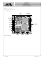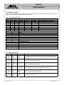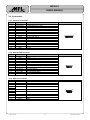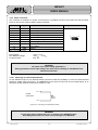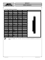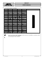
1
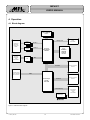
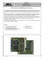
MIP405T
USERS MANUAL
MPL Industrial PC with IBM PowerPC™ Processor
The MIP405T is a highly integrated industrial single board computer in PC/104 form factor. Build around the
PPC405 IBM PowerPC™ Processor it is well suited for applications requiring small size, high performance
and Low Power. The MIP405T can be used in a standard operating environment without the necessity of a
fan.
All major components required to build a industrial PC system are implemented on a single PC/104 sized
board. It features one E-IDE, one 10/100Base TX Ethernet, two serial ports, and a real time clock. The 16bit PC/104 (ISA) and the PC/104+ (PCI) interface offers easy and flexible expansion capabilities.
Integration of the MIP405T into a system is facilitated by the fact of offering standard a connector E-IDE (44
pin header). The serial interfaces as can be accessed through 2mm pin headers. Particular precaution has
been taken to the EMC so that an entire system can fulfill the CE and FCC requirements.
The SDRAM is soldered on board.
All these features make the MIP405T to the ideal solution for any low-cost embedded control application
where a flexible industrial PC is needed.
Features
•
•
•
•
•
•
•
•
Low Power IBM PPC405 Processor
Processor clock up to 400 MHz
Up to 128MByte SDRAM on board.
Integrated 10/100 Mbit/s Ethernet Controller
PC/104 and PC/104 Plus interface
© 2005 by MPL AG
1
One EIDE HDD ports
Two RS232 ports
Low power consumption
MIP405T
USERS MANUAL
TABLE OF CONTENTS
1.
1.1
1.2
1.3
1.4
2.
2.1
2.2
3.
INTRODUCTION.........................................................................................................................................3
About this manual ..................................................................................................................................3
Safety precautions and handling ...........................................................................................................3
Electrostatic discharge (ESD) protection...............................................................................................3
Equipment safety ...................................................................................................................................3
GENERAL INFORMATION AND SPECIFICATIONS.................................................................................4
Specifications.........................................................................................................................................4
Dimensions ............................................................................................................................................6
PREPARATION FOR USE .........................................................................................................................7
3.1 Parts location .........................................................................................................................................7
3.2 Switch settings .......................................................................................................................................8
3.2.1
Configuration Switch .....................................................................................................................8
3.3 LED Indicators .......................................................................................................................................8
3.4 Connectors.............................................................................................................................................9
3.4.1
Serial port connector.....................................................................................................................9
3.4.2
Debug/JTAG connector ................................................................................................................9
3.4.3
Ethernet Connector.......................................................................................................................9
3.4.4
Power Connector ........................................................................................................................10
3.4.4.1
Mounting an external Reset Switch........................................................................................10
3.4.5
PC104 interface pin numbers .....................................................................................................11
3.4.6
PC104+ Interface pin numbers ...................................................................................................12
3.4.7
E-IDE connector..........................................................................................................................13
4.
OPERATION .............................................................................................................................................14
4.1 Block diagram ......................................................................................................................................14
4.2 Interrupts..............................................................................................................................................15
4.2.1
CPU Interrupts ............................................................................................................................15
4.2.2
ISA Interrupts ..............................................................................................................................15
4.3 Extension registers ..............................................................................................................................16
4.3.1
PLD Partnumber Register...........................................................................................................16
4.3.2
PLD Version Register .................................................................................................................16
4.3.3
Board Revision and Config Register...........................................................................................16
4.3.4
IRQ Register ...............................................................................................................................17
4.3.5
Communication Mode Register ..................................................................................................17
4.3.6
Configuration Switch Register.....................................................................................................17
5.
5.1
5.2
SUPPORT INFORMATION ......................................................................................................................18
MPL AG ...............................................................................................................................................18
Production serial and revision number ................................................................................................18
© 2005 by MPL AG
2
MEH-10098-001 Rev. B
MIP405T
USERS MANUAL
1. Introduction
1.1 About this manual
This manual assists the installation and initialization procedure by providing all hardware related information
necessary to handle and configure the MIP405T.
For all bootloader related information please refer to the PPCBoot for the MIP405T User Manual (MEH10082-002) supplied by MPL AG or your local MIP405T supplier. The PPCBoot for MIP405T User Manual is
also available on the internet under "http://www.mpl.ch" in PDF format.
The manual is written for technical personnel responsible for integrating the MIP405T into their system.
1.2 Safety precautions and handling
For personal safety and safe operation of the MIP405T, follow all safety procedures described here and in
other sections of the manual.
• Power must be removed from the system before installing (or removing) the MIP405T to prevent the
possibility of personal injury (electrical shock) and/or damage to the product.
• Handle the product carefully, i.e., dropping or mishandling the MIP405T can cause damage to assemblies
and .
• Do not expose the equipment to moisture.
WARNING
There are no user-serviceable components on the MIP405T
1.3 Electrostatic discharge (ESD) protection
Various electrical components within the product are sensitive to static and electrostatic discharge (ESD).
Even a non-sensible static discharge can be sufficient to destroy or degrade a component's operation!
1.4 Equipment safety
Great care is taken by MPL that all its products are thoroughly and rigorously tested before leaving the
factory to ensure that they are fully operational and conform to specification. However, no matter how reliable
a product, there is always the remote possibility that a defect may occur. The occurrence of a defect on this
device may, under certain conditions, cause a defect to occur in adjoining and/or connected equipment. It is
the user’s responsibility to ensure that adequate protection for such equipment is incorporated when
installing this device. MPL accepts no responsibility whatsoever for such kind of defects, however caused.
© 2005 by MPL AG
3
MEH-10098-001 Rev. B
MIP405T
USERS MANUAL
2. General information and specifications
This chapter provides a general overview over the MIP405T and its features. It outlines the electrical and
physical specifications of the product, its power requirements and a list of related publications.
2.1 Specifications
Electrical
Processor:
• IBM PPC405GPr PowerPC™ 32Bit RISC Processor
• Separate, configurable, two-way set-associative instruction (16 kByte) and data (16 kByte) cache units
• Technology: IBM CMOS SA-27E, 0.18 Micron Process Technology
• Clock frequency up to 400 MHz
• Very low power consumption
Bootloader ROM:
• Up to 8MB Flash EEPROM
• 512kB PPCBoot (open source) boot loader
• Easy boot loader update
Memory:
• Up to 128MByte soldered SDRAM on board
RTC:
• backed with external battery
• Year 2000 compliant
PC/104 /Plus interface:
• ISA bridge Intel 82371EB (Southbridge)
• 16 Bit PC/104 interface
• 32 Bit PC/104 Plus interface
Serial ports:
• 1 RS232 port with full modem handshake
• 1 selectable port RS232 / TTL
• RS232 transfer rates up to 230 kBaud
• TTL transfer rates up to 1.15 MBaud
• Available on 16pin 2mm header
E-IDE port:
• Up to 2 drives
• Available on 44 pin header, 2 mm pitch, for 2,5” Notebook hard disk.
• PIO Mode 4 and Bus Master IDE, transfers up to 14 Mbytes/s
• Ultra DMA/33 mode, synchronous DMA mode transfers up to 33 Mbytes/s
• Activity indicator on board
© 2005 by MPL AG
4
MEH-10098-001 Rev. B
MIP405T
USERS MANUAL
Ethernet:
• PPC405 integrated 10/100 MBit/s Ethernet Controller
• IEEE802.3 10BASE-T and 100BASE-TX compatible
• IEEE 802.3u Autonegotiation Support
• IEEE 802.3x 100BASE-TX Flow Control support
• Activity indicators for link detection/network traffic and 100 Mbit/s operation on board
Indicators:
• Power LED (green)
• Reset / Power Fail LED (red)
• Error LED (red)
• HDD activity LED (green)
• LAN LED (green)
• 1 user programmable LED (green)
PHYSICAL/POWER
Form factor:
PC/104, with connectors in defined I/O connectors overhang regions
Length: 95.89 mm (3.775 inches)
Width: 90.17 mm (3.550 inches)
Height: 8.5 mm (0.335 inch) (excluding PC/104 bus connectors)
Weight:
ca. 80g
Power supply:
Over PC/104 bus interface or through separate 10-pin 2,54mm header connector.
Input Power requirement:
+5V:
+5VDC ± 5%
Power consumption:
t.b.d.
ENVIRONMENT
Temperature range:
-40°C to +85°C (-40°F to +185°F)
Relative humidity:
10% ... 90% non condensing
© 2005 by MPL AG
5
MEH-10098-001 Rev. B
MIP405T
USERS MANUAL
2.2 Dimensions
90,17
85,09
78,62
61,98
52,58
43,18
33,78
24,38
14,99
2,54
5,08
5,08
0
22,00
48,00
70,40
91,19
95,89
2,50
1
2
3
4
5
6
7
8
2,50
O
N
7,62
81,28
Figure 2.2.1 Dimensions MIP405T
© 2005 by MPL AG
6
MEH-10098-001 Rev. B
MIP405T
USERS MANUAL
3. Preparation for use
3.1 Parts location
EIDE
Connector
2
9
10
1
2
Power
Connector
LED6
O
N
1
43
44
1
2
3
4
5
6
7
8
1
Configuration
Switch
1
00
LED5
PC104 Plus
(PCI) Connector
PC104 (IDE)
Connector
LED4
LED3
LED2
LED1
30
19
DC
ABCD
30
AB
16
15
2
1
Serial
Connector
12 2
11 1
2
1
Ethernet
Connector
12
11
Debug / JTAG
Connector
Figure 3.1.1 Parts location
© 2005 by MPL AG
7
MEH-10098-001 Rev. B
MIP405T
USERS MANUAL
3.2 Switch settings
Default switch settings are bold. Please note, that modifications of the switches during operation have no
effect. The changes become valid after the next reset.
3.2.1 Configuration Switch
PPC405 PLL Settings
S1
S2
S3
OFF
OFF
OFF
OFF
OFF
ON
OFF
ON
OFF
OFF
ON
ON
ON
OFF
OFF
ON
OFF
ON
ON
ON
OFF
ON
ON
ON
S4
ON
OFF
S5
ON
OFF
S6
ON
OFF
S7
ON
OFF
S8
ON
OFF
CPU
PLB
OPB
132 MHz
66 MHz
16.5 MHz
165 MHz
66 MHz
16.5 MHz
198 MHz
99 MHz
24.75 MHz
247.5 MHz 99 MHz
24.75 MHz
264 MHz
132 MHz
33 MHz
297 MHz
99 MHz
24.75 MHz
330 MHz
132 MHz
33 MHz
396 MHz
132 MHz
33 MHz
Serial Port 1 Interface Mode
TTL
RS232
EEPROM write protection
Write protected
Unprotected
FLASH write protection
Write protected
Unprotected
User Configuration 1
User defined
User defined
User Configuration 2
User defined
User defined
PPC405 processor
GPr-266/333/400, GP-200/266
GPr-266/333/400
GPr-266/333/400, GP-200/266
GPr-266/333/400
GPr-266/333/400, GP-266
GPr-333/400
GPr-333/400
GPr-400
Table 3.2.1Configuration Switch
3.3 LED Indicators
Ref
Color
Function
Description
LED6
Green
USER
Lit if ULED bit is set in extension register COM_Mode (please refer
to 4.3.5)
LED5
Green
LAN
Lit when LAN activity is detected
LED4
Green
IDE
Lit when IDE activity is detected
LED3
Red
EXEPTION
Lit when PPC405 has detected an Error (Sys_Error)
LED2
Red
RESET
Lit when PPC405 is in Reset state
LED1
Green
POWER
Lit when 5V power is Ok
Table 3.3.1 Indicators
© 2005 by MPL AG
8
MEH-10098-001 Rev. B
MIP405T
USERS MANUAL
3.4 Connectors
3.4.1 Serial port connector
Number Signal
1
RXD1 (TTL)
2
TXD1 (TTL)
3
RXD1
4
TXD1
5
RTS1/DTR1
6
CTS1/DSR1
7
DCD0
8
DSR0
9
RXD0
10
RTS0
11
TXD0
12
CTS0
13
DTR0
14
RI0
15
GND
16
GND
Description
Receive Data, Port 1 (TTL)
Transmit Data, Port 1 (TTL)
Receive Data, Port 1
Transmit Data, Port 1
Request to Send or Data Terminal Ready, Port 1
Clear to Send or Data Set Ready, Port 1
Carrier Detect, Port 0
Data Set Ready, Port 0
Receive Data, Port 0
Request to Send, Port 0
Transmit Data, Port 0
Clear to Send, Port 0
Data Terminal Ready, Port 0
Ring Indicator, Port 0
Ground
Ground
Pinout
16
15
2
1
Table 3.4.1 Serial Port Connector
3.4.2 Debug/JTAG connector
Number Signal
1
VCC5
2
GND
3
CPU TDO
4
CPU TDI
5
CPU_TRST#
6
CPU_TCK
7
CPU TMS
8
CPU HALT#
9
PLD TDI
10
PLD TDO
11
PLD TMS
12
PLD TCK
Description
5V power supply
Ground
CPU JTAG Data Out
CPU JTAG Data In
CPU JTAG Reset
CPU JTAG Clock
CPU JTAG Mode Select
CPU Halt
PLD JTAG Data In
PLD JTAG Data Out
PLD JTAG Mode Select
PLD JTAG Clock
Pinout
12
11
2
1
Table 3.4.2 Debug/JTAG connector
3.4.3 Ethernet Connector
Number Signal
1
TX+
2
TX3
RX+
4
TERM1
5
6
RX7
TERM2
8
9
NC
10
NC
11
EARTH
12
EARTH
Description
Pinout
Transmit Data +
Transmit Data Receive Data +
Common Mode Termination 1
Receive Data -
2
1
Common Mode Termination 2
12
11
Shield
Shield
Table 3.4.3 10/100Base TX Header
© 2005 by MPL AG
9
MEH-10098-001 Rev. B
MIP405T
USERS MANUAL
3.4.4 Power Connector
This connector is needed if no power via PC104 bus is provided. No other inputs than this and the power
inputs on PC104 bus must be used to power the board.
Pin number
Signal
1
2
3
4
5
6
7
8
9
10
GND
VIN
GND
VIN
SRESET#
VRTC
VIN
GND
VIN
GND
Description
Pinout
Ground
Input voltage
Ground
Input voltage
System Reset Input (active low)
RTC Backup Voltage
Input voltage
Ground
Input voltage
Ground
2
1
10
9
Table 3.4.4 Power connector
Input Voltage :
RTC Backup Voltage:
Contact Current:
+5VDC (+-5%)
+2.5VDC ... +4.5VDC
max. 3A
WARNING
Be aware of the input voltage polarization !
Wrong polarization of the input voltage can cause serious damage to the MIP405T and
attached peripherals!
3.4.4.1 Mounting an external Reset Switch
On the SRESET# input on the External Power Connector exists the possibility to mount an external Reset
Switch for system reset, see Figure . The SRESET# input is active low and can be connected directly to an
open drain output (internal 10kΩ pull up resistor to 3.3V).
Pin 3
Power
Connector
Reset
Button
Pin 5
Figure 3.4.4.1 Mounting an External Reset Switch
WARNING
Do not apply other voltages than Vin- or tristate to the SRESET# input!
Exceeding these limits can cause serious damage to the MIP405T!
© 2005 by MPL AG
10
MEH-10098-001 Rev. B
MIP405T
USERS MANUAL
3.4.5 PC104 interface pin numbers
Number
0
1
2
3
4
5
6
7
8
9
10
11
12
13
14
15
16
17
18
19
20
21
22
23
24
25
26
27
28
29
30
31
32
Row A
-/IOCHCK
SD7
SD6
SD5
SD4
SD3
SD2
SD1
SD0
IOCHRDY
AEN
SA19
SA18
SA17
SA16
SA15
SA14
SA13
SA12
SA11
SA10
SA9
SA8
SA7
SA6
SA5
SA4
SA3
SA2
SA1
SA0
GND
Row B
-GND
RSTDRV
+5V
IRQ9
(-5V) 1
DRQ2
(-12V) 1
/ENDXFR
(+12V) 1
NC
/SMEMW
/SMEMR
/IOW
/IOR
/DACK3
DRQ3
/DACK1
DRQ1
/REFRESH
SYSCLK
IRQ7
IRQ6
IRQ5
IRQ4
IRQ3
/DACK2
TC
BALE
+5V
OSC
GND
GND
Row C
GND
/SBHE
LA23
LA22
LA21
LA20
LA19
LA18
LA17
/MEMR
/MEMW
SD8
SD9
SD10
SD11
SD12
SD13
SD14
SD15
NC
--------------
Row D
GND
/MEMCS16
/IOCS16
IRQ10
IRQ11
IRQ12
IRQ15
IRQ14
/DACK0
DRQ0
/DACK5
DRQ5
/DACK6
DRQ6
/DACK7
DRQ7
+5V
(/MASTER) 1
GND
GND
--------------
Pinout
AB
1
DC
0
19
32
Table 3.4.5 PC/104 connector
Notes:
1
© 2005 by MPL AG
Signal not available. (-5V, +12V and -12V are not connected and /MASTER is pulled-down to
GND)
11
MEH-10098-001 Rev. B
MIP405T
USERS MANUAL
3.4.6 PC104+ Interface pin numbers
Number
1
2
3
4
5
6
7
8
9
10
11
12
13
14
15
16
17
18
19
20
21
22
23
24
25
26
27
28
29
30
Row A
GND
+5V
AD5
C/BE0
GND
AD11
AD14
(+3.3V)2
SERR
GND
STOP
(+3.3V) 2
FRAME
GND
AD18
AD21
(+3.3V) 2
IDSEL0
AD24
GND
AD29
+5V
REQ0
GND
GNT1
+5V
CLK2
GND
(+12V) 1
(-12V) 1
Row B
NC
AD2
GND
AD7
AD9
+5V
AD13
C/BE1
GND
PERR
(+3.3V) 2
TRDY
GND
AD16
(+3.3V) 2
AD20
AD23
GND
C/BE3
AD26
+5V
AD30
GND
REQ2
+5V
CLK0
+5V
INTD
INTA
NC
Row C
+5V
AD1
AD4
GND
AD8
AD10
GND
AD15
(SBO) 1
(+3.3V) 2
(LOCK) 1
GND
IRDY
(+3.3V) 2
AD17
GND
AD22
IDSEL1
+5V
AD25
AD28
GND
REQ1
+5V
GNT2
GND
CLK3
+5V
INTB
NC
Row D
AD0
+5V
AD3
AD6
GND
(M66EN) 1
AD12
(+3.3V) 2
PAR
(SDONE) 1
GND
DEVSEL
(+3.3V) 2
C/BE2
GND
AD19
(+3.3V) 2
IDSEL2
IDSEL3
GND
AD27
AD31
+5V
GNT0
GND
CLK1
GND
RST
INTC
GND
Pinout
ABCD
1
30
Table 3.4.6 PC/104 Plus connector
Notes:
1
2
© 2005 by MPL AG
Signal not available. (SBO, SDONE and LOCK are pull-up to 5V, M66EN is connected to GND
and +12V and -12V are not connected).
3.3V power pins are not connected.
12
MEH-10098-001 Rev. B
MIP405T
USERS MANUAL
3.4.7 E-IDE connector
Pin
1
3
5
7
9
11
13
15
17
19
21
23
25
27
29
31
33
35
37
39
41
43
Signal
/RESET
D7
D6
D5
D4
D3
D2
D1
D0
GND
DRQ
IOW
IOR
IORDY
DACK
IRQ
A1
A0
CS0
ACTLED
VCC
GND
Description
Reset
Data bit 7
Data bit 6
Data bit 5
Data bit 4
Data bit 3
Data bit 2
Data bit 1
Data bit 0
Ground
DMA request
I/O write strobe
I/O read strobe
I/O ready
DMA acknowledge
Interrupt request
Address 1
Address 0
Chipselect 0
Activity LED
+5V
Ground
Pin
2
4
6
8
10
12
14
16
18
20
22
24
26
28
30
32
34
36
38
40
42
44
Signal
GND
D8
D9
D10
D11
D12
D13
D14
D15
KEY
GND
GND
GND
HDBALE
GND
IOCS16
NC
A2
CS1
GND
VCC
GND
Description
Ground
Data bit 8
Data bit 9
Data bit 10
Data bit 11
Data bit 12
Data bit 13
Data bit 14
Data bit 15
Key / not connected
Ground
Ground
Ground
Spindle sync / cable select
Ground
I/O chipselect16
Not connected
Address 2
Chipselect 1
Ground
+5V
Ground
Table 3.4.7 EIDE connectors
© 2005 by MPL AG
13
MEH-10098-001 Rev. B
MIP405T
USERS MANUAL
4. Operation
4.1 Block diagram
Up to 8MByte
Up
to 8MByte
Flash
Flash
Debug Port
Serial Port
Connector:
16 pin 2mm
header
Ethernet
Connector:
12 pin
2mm header
RS232
Interface
RS232
Interface
RS232
Interface
RS232
Interface
100MBit
PHY
100MBit
PHY
Serial 0
Serial 1
PowerPC
PowerPC
PPC405GPr
PPC405GPr
266MHz
266MHz
Up to
Up to
128MByte
128MByte
SDRAM
SDRAM
soldered
soldered
onboard
onboard
MII
PCI Bus
EIDE Connector:
44-pin Flat Cable
2mm Connector
Debug Connector:
12 pin
2mm header
PC/104+ Connector
PCI Part
IDE0
Southbridge
Southbridge
PIIX4E
PIIX4E
82371EB
82371EB
ISA Bus
PC/104+ Connector
ISA Part
RTC Backup
Power /Reset
Connector:
12 pin
2mm header
Onboard
PowerOnboard
Supply
Power Supply
Figure 4.1 MIP405T Block Diagram
© 2005 by MPL AG
14
MEH-10098-001 Rev. B
MIP405T
USERS MANUAL
4.2 Interrupts
4.2.1 CPU Interrupts
The PPC405 provides 7 Interrupts. They are distributed as follows:
CPU IRQ IRQ Source
Source
0
INTR# (PIIX4E Interrupt Controller )
EPLD
1
Not used
EPLD
2
SMI# , INIT# and NMI#
EPLD
3
PCI_INTA#
PCI Bus
4
PCI_INTB#
PCI Bus
5
PCI_INTC#
PCI Bus
6
PCI_INTD#
PCI Bus
Table 4.2.1 CPU Interrupts
Note:
• The 3 Interrupts from the EPLD are routed as follows:
• INTR# is the inverted INTR Signal form the PIIX4E Interrupt Controller
• NMI# is the inverted NMI Signal from the PIIX4E
• SMI# is the PIIX4E SMI# Signal
4.2.2 ISA Interrupts
The ISA Interrupts are routed as follows:
IRQs
Device
IRQ0
Timer
IRQ1
Free
IRQ2
2nd IRQ Controller
IRQ3
Free
IRQ4
Free
IRQ5
Free
IRQ6
Free
IRQ7
Free
IRQ8
RTC
IRQ9
Free
IRQ10
Free
IRQ11
Free
IRQ12
Free
IRQ13
Free
IRQ14
Primary IDE
IRQ15
Secondary IDE
Remarks
PIIX4E Internal, not available
PIIX4E Internal, not available
PIIX4E Internal, not available
Not Maskable
Not Maskable
Table 4.2.2 ISA Interrupts
© 2005 by MPL AG
15
MEH-10098-001 Rev. B
MIP405T
USERS MANUAL
4.3 Extension registers
The PLD is located at the CS7# on the peripheral local bus. The bit notations are in big Endian Format (That
is D0 MSB, D7 LSB)
Offset Name
Type
Function
5
EXT_REG
Read only
Config Register
4
COM_MODE
Read/Write
Communication Mode Register
3
IRQ_REG
Read only
IRQ Register
2
BOARD_REV
Read only
Board Revision and populated Configuration
1
PLD_VERS
Read only
Versions Number of the PLDs
0
PLD_PART
Read only
Part Number of the PLDs
Table 4.3 Extensions Registers
4.3.1 PLD Partnumber Register
Read
Default
D0
MIPID
1
PLD_PART
D1
0
D2
0
PLD_CS# + 0x00
D3
D4
D5
PLD Part Number
0
0
0
Read Only
D6
D7
0
0
Table 4.3.1 PLD Partnumber register
MIPID:
PLD Part Number:
MIP405 product identification bit. 0=MIP405, 1=MIP405T
is the Part Index of the PLD.
4.3.2 PLD Version Register
D0
Read
Default
PLD_VERS
D1
0
0
D2
0
PLD_CS# + 0x01
D3
D4
D5
PLD Version Number
0
0
0
Read Only
D6
D7
0
0
Table 4.3.2 PLD Version Register
PLD Version Number is the Version Number of the PLD.
4.3.3 Board Revision and Config Register
Read
Default
D0
PCB0
0
BOARD_REV
D1
D2
PCB1
PCB2
0
0
D3
PCB3
0
PLD_CS# + 0x02
D4
D5
CFG0
CFG1
X
X
Read Only
D6
D7
CFG2
CFG3
X
X
Table 4.3.3 Board Revision and Config Register
PCBx:
CFGx:
CFG0..3
0001
© 2005 by MPL AG
Binary decoded PCB Revision. Add an ASCII ‘A’ to this number to get the PCB Revision.
Currently PCB3..0 = 0 => ‘A’.
Config Inputs. Used to distinguish different population or other Options.:
Option
MIP405T-1 (GPr-266 MHz, 64MByte SDRAM, 4 Mbyte FLASH
16
MEH-10098-001 Rev. B
MIP405T
USERS MANUAL
4.3.4 IRQ Register
D0
INTR#
1
Read
Default
IRQ_REG
D1
D2
Reserved Reserved
0
0
D3
SMI#
1
PLD_CS# + 0x03
D4
D5
INIT#
NMI#
1
1
Read Only
D6
D7
Reserved Reserved
1
1
Table 4.3.4 IRQ Register
INTR#:
SMI#:
Interrupt from PIIX4E. (Low Active) Will be forwarded to the PPC405 on INT0#
System Management Interrupt from PIIX4E. (Low Active) Will be forwarded to the PPC405 on
INT2#
Init Output from PIIX4E. (Low Active) Will be forwarded to the PPC405 on INT2#
Non maskable Interrupt from PIIX4E. (Low Active) Will be forwarded to the PPC405 on INT2#
INIT#:
NMI#:
4.3.5 Communication Mode Register
D0
Reserved
Reserved
0
Read
Write
Default
COM_MODE
D1
S0
S0
0
D2
S1
S1
0
D3
S2
S2
0
PLD_CS# + 0x04
D4
D5
Reserved
ULED
Reserved
ULED
0
0
Read / Write
D6
D7
Reserved IDERST
Reserved IDERST
0
0
Table 4.3.5 Communication Mode Register
SER1ALT: Alternate SER1 Hardware Handshake. If set, the SER1 uses DTR, DSR Handshaking instead of
CTS, RTS. If this Bit is set, clear the Bit DCS, and set the bit RDS in the Register CHCR0 of the
PPC405.
S[2..0]:
Binary encoded value for the UARTSERCLK clock input of the PPC405.
S2
S1
S0
Clock nom.
Clock eff.
0
0
0
0
1
1
1
1
0
0
1
1
0
0
1
1
0
1
0
1
0
1
0
1
7.3728 MHz
11.0592 MHz
12 MHz
18.432 MHz
22.1184 MHz
24 MHz
36.864 MHz
40 MHz
7.3977 MHz
11.064 MHz
12.002 MHz
18.435 MHz
22.114 MHz
23.996 MHz
36.869 MHz
39.992 MHz
ULED:
Error
ppm
3381
438
167
144
215
158
144
196
If set, the User LED is switched on.
4.3.6 Configuration Switch Register
Read
D0
S1-1
DIP Switch
D1
S1-2
D2
S1-3
D3
S1-4
PLD_CS# + 0x05
D4
D5
S1-5
S1-6
Read Only
D6
D7
S1-7
S1-8
Table 4.3.6 Configuration Switch Register
© 2005 by MPL AG
17
MEH-10098-001 Rev. B
MIP405T
USERS MANUAL
5. Support information
5.1 MPL AG
In case of questions contact MPL AG or your local distributor.
MPL AG homepage:
Email address:
www.mpl.ch
[email protected]
5.2 Production serial and revision number
To get the actual production revision number of your device, please see the label on the bottom of the
MIP405T Board.
MIP405T-1
S/N: 100 [A]
Production
Serial Number
© 2005 by MPL AG
Production
Revision Number
18
MEH-10098-001 Rev. B
MIP405T
USERS MANUAL
This page is left blank intentionally.
© 2005 by MPL AG
19
MEH-10098-001 Rev. B
MIP405T
USERS MANUAL
Copyright and revision history
Copyright © 2005 by MPL AG Elektronik Unternehmen. All rights reserved. Reproduction of this document in
part or whole, by any means is prohibited, without written permission from MPL AG Elektronik Unternehmen.
This manual reflects Revision A of the MIP405T.
Disclaimer
The information contained herein is believed to be accurate as of the date of this publication, however, MPL
AG will not be liable for any damages, including indirect or consequential, arising out of the application or use
of any product, circuit or software described herein.
MPL AG reserves the right to make changes to any product herein to improve reliability, function or design.
Trademarks
Brand or product names are trademarks and registered trademarks of their respective holders.
Our local distributor:
© 2005 by MPL AG
20
MEH-10098-001 Rev. B