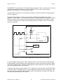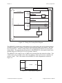
1
™
DAQCard -500
User Manual
Multifunction I/O Card for Type II PCMCIA Bus
January 1996 Edition
Part Number 371918A-01
© Copyright 1995, 1996 National Instruments Corporation.
All Rights Reserved.
National Instruments Corporate Headquarters
6504 Bridge Point Parkway
Austin, TX 78730-5039
(512) 794-0100
Technical support fax: (800) 328-2203
(512) 794-5678
Branch Offices:
Australia 03 9 879 9422, Austria 0662 45 79 90 0, Belgium 02 757 00 20, Canada (Ontario) 519 622 9310,
Canada (Québec) 514 694 8521, Denmark 45 76 26 00, Finland 90 527 2321, France 1 48 14 24 24,
Germany 089 741 31 30, Hong Kong 2645 3186, Italy 02 48301892, Japan 03 5472 2970, Korea 02 596 7456,
Mexico 95 800 010 0793, Netherlands 0348 433466, Norway 32 84 84 00, Singapore 2265886, Spain 91 640 0085,
Sweden 08 730 49 70, Switzerland 056 200 51 51, Taiwan 02 377 1200, U.K. 01635 523545
Limited Warranty
The DAQCard-500 is warranted against defects in materials and workmanship for a period of one year from the date
of shipment, as evidenced by receipts or other documentation. National Instruments will, at its option, repair or
replace equipment that proves to be defective during the warranty period. This warranty includes parts and labor.
The media on which you receive National Instruments software are warranted not to fail to execute programming
instructions, due to defects in materials and workmanship, for a period of 90 days from date of shipment, as
evidenced by receipts or other documentation. National Instruments will, at its option, repair or replace software
media that do not execute programming instructions if National Instruments receives notice of such defects during
the warranty period. National Instruments does not warrant that the operation of the software shall be uninterrupted
or error free.
A Return Material Authorization (RMA) number must be obtained from the factory and clearly marked on the
outside of the package before any equipment will be accepted for warranty work. National Instruments will pay the
shipping costs of returning to the owner parts which are covered by warranty.
National Instruments believes that the information in this manual is accurate. The document has been carefully
reviewed for technical accuracy. In the event that technical or typographical errors exist, National Instruments
reserves the right to make changes to subsequent editions of this document without prior notice to holders of this
edition. The reader should consult National Instruments if errors are suspected. In no event shall National
Instruments be liable for any damages arising out of or related to this document or the information contained in it.
EXCEPT AS SPECIFIED HEREIN, NATIONAL INSTRUMENTS MAKES NO WARRANTIES, EXPRESS OR IMPLIED,
AND SPECIFICALLY DISCLAIMS ANY WARRANTY OF MERCHANTABILITY OR FITNESS FOR A PARTICULAR
PURPOSE . CUSTOMER’S RIGHT TO RECOVER DAMAGES CAUSED BY FAULT OR NEGLIGENCE ON THE PART
OF NATIONAL INSTRUMENTS SHALL BE LIMITED TO THE AMOUNT THERETOFORE PAID BY THE CUSTOMER.
NATIONAL INSTRUMENTS WILL NOT BE LIABLE FOR DAMAGES RESULTING FROM LOSS OF DATA, PROFITS,
USE OF PRODUCTS, OR INCIDENTAL OR CONSEQUENTIAL DAMAGES, EVEN IF ADVISED OF THE POSSIBILITY
THEREOF. This limitation of the liability of National Instruments will apply regardless of the form of action,
whether in contract or tort, including negligence. Any action against National Instruments must be brought within
one year after the cause of action accrues. National Instruments shall not be liable for any delay in performance due
to causes beyond its reasonable control. The warranty provided herein does not cover damages, defects,
malfunctions, or service failures caused by owner’s failure to follow the National Instruments installation, operation,
or maintenance instructions; owner’s modification of the product; owner’s abuse, misuse, or negligent acts; and
power failure or surges, fire, flood, accident, actions of third parties, or other events outside reasonable control.
Copyright
Under the copyright laws, this publication may not be reproduced or transmitted in any form, electronic or
mechanical, including photocopying, recording, storing in an information retrieval system, or translating, in whole
or in part, without the prior written consent of National Instruments Corporation.
Trademarks
LabVIEW ®, NI-DAQ ®, RTSI ®, and DAQCard ™ are trademarks of National Instruments Corporation.
Product and company names listed are trademarks or trade names of their respective companies.
WARNING REGARDING MEDICAL AND CLINICAL USE
OF NATIONAL INSTRUMENTS PRODUCTS
National Instruments products are not designed with components and testing intended to ensure a level of reliability
suitable for use in treatment and diagnosis of humans. Applications of National Instruments products involving
medical or clinical treatment can create a potential for accidental injury caused by product failure, or by errors on
the part of the user or application designer. Any use or application of National Instruments products for or involving
medical or clinical treatment must be performed by properly trained and qualified medical personnel, and all
traditional medical safeguards, equipment, and procedures that are appropriate in the particular situation to prevent
serious injury or death should always continue to be used when National Instruments products are being used.
National Instruments products are NOT intended to be a substitute for any form of established process, procedure, or
equipment used to monitor or safeguard human health and safety in medical or clinical treatment.
Contents
____________________________________________________
About This Manual............................................................................................................. ix
Organization of This Manual ......................................................................................... ix
Conventions Used in This Manual................................................................................. x
National Instruments Documentation ........................................................................... x
Related Documentation.................................................................................................. xi
Customer Communication ............................................................................................. xi
Chapter 1
Introduction .......................................................................................................................... 1-1
About the DAQCard-500............................................................................................... 1-1
What You Need to Get Started ...................................................................................... 1-2
Software Programming Choices .................................................................................... 1-2
LabVIEW and LabWindows/CVI Application Software .................................. 1-2
NI-DAQ Driver Software................................................................................... 1-3
Register-Level Programming............................................................................. 1-4
Optional Equipment ....................................................................................................... 1-4
Unpacking ...................................................................................................................... 1-4
Chapter 2
Installation and Configuration....................................................................................... 2-1
Installation...................................................................................................................... 2-1
Configuration ................................................................................................................. 2-2
Analog Input Configuration...............................................................................2-3
Digital I/O Configuration...................................................................................2-3
Counter Configuration .......................................................................................2-3
Chapter 3
Signal Connections ............................................................................................................. 3-1
I/O Connector................................................................................................................. 3-1
Signal Connection Descriptions..................................................................................... 3-2
Analog Input Signal Connections ...................................................................... 3-2
Analog Input Signal Connection Considerations...................................3-3
Types of Signal Sources.........................................................................3-3
Ground-Referenced Signal Sources...........................................3-3
Floating Signal Sources .............................................................3-3
Types of Measurement Systems ............................................................3-3
Ground-Referenced Measurement System ................................3-4
Floating Measurement System...................................................3-4
Analog Input Configurations .................................................................3-4
Digital I/O Signal Connections..........................................................................3-5
Timing Connections...........................................................................................3-7
Data Acquisition Counter and Timing Connections..............................3-7
General-Purpose Counter and Timing Signal Connections ...................3-7
Cabling...........................................................................................................................3-11
© National Instruments Corporation
v
DAQCard-500 User Manual
Contents
Chapter 4
Theory of Operation .......................................................................................................... 4-1
Functional Overview......................................................................................................4-1
PCMCIA I/O Channel Interface Circuitry.....................................................................4-2
Analog Input and Data Acquisition Circuitry................................................................4-3
Analog Input Circuitry.......................................................................................4-3
Data Acquisition Timing Circuitry ....................................................................4-4
Single-Channel Data Acquisition...........................................................4-4
Multichannel (Scanned) Data Acquisition.............................................4-5
Data Acquisition Rates...........................................................................4-5
Digital I/O Circuitry.......................................................................................................4-5
Timing I/O Circuitry ......................................................................................................4-6
Appendix A
Specifications ........................................................................................................................ A-1
Appendix B
Differences between the DAQCard-700 and the DAQCard-500 ....................... B-1
Appendix C
Custom Cable Design......................................................................................................... C-1
Appendix D
PC Card Questions and Answers .................................................................................. D-1
Appendix E
Power Management Modes ............................................................................................. E-1
Appendix F
PSH27-50F Signal Connections ..................................................................................... F-1
Appendix G
Customer Communication............................................................................................... G-1
Glossary ......................................................................................................................Glossary-1
Index ................................................................................................................................. Index-1
DAQCard-500 User Manual
vi
© National Instruments Corporation
Contents
Figures
Figure 1-1.
The Relationship between the Programming Environment, NI-DAQ,
and Your Hardware.............................................................................................. 1-3
Figure 2-1.
A Typical Configuration for the DAQCard-500 ................................................ 2-2
Figure 3-1.
Figure 3-2.
Figure 3-3.
Figure 3-4.
Figure 3-5.
Figure 3-6.
Figure 3-7.
I/O Connector Pin Assignments .......................................................................... 3-1
DAQCard-500 Analog Input Connections .......................................................... 3-5
Digital I/O Signal Connections............................................................................ 3-6
EXTCONV* Signal Timing ................................................................................ 3-7
Event-Counting Applications with External Switch Gating................................ 3-8
Frequency Measurement Application.................................................................. 3-9
General-Purpose Timing Signals......................................................................... 3-10
Figure 4-1.
Figure 4-2.
Figure 4-3.
Figure 4-4.
Figure 4-5.
Figure 4-6.
DAQCard-500 Block Diagram............................................................................ 4-1
PCMCIA I/O Interface Circuitry Block Diagram ............................................... 4-2
Analog Input and Data Acquisition Circuitry Block Diagram ............................ 4-3
Digital I/O Circuitry Block Diagram................................................................... 4-6
Timing I/O Circuitry Block Diagram .................................................................. 4-7
Counter Block Diagram....................................................................................... 4-7
Figure C-1. DAQCard-500 I/O Connector Pin Assignments.................................................. C-2
Figure F-1.
CB-50 Pin Assignments Using the PSH27-50F-D1 Cable.................................. F-1
Tables
Table 3-1.
Recommended Input Configurations for Ground-Referenced and
Floating Measurement Systems...........................................................................3-4
Table E-1.
DAQCard-500 Power-Management Modes.........................................................E-1
© National Instruments Corporation
vii
DAQCard-500 User Manual
About This Manual
This manual describes the mechanical and electrical aspects of the DAQCard-500 and contains
information concerning its installation and operation. The DAQCard-500 is a compact, low-cost,
low-power analog input, digital I/O, and timing I/O board for computers that are equipped with a
Type II PCMCIA socket.
Organization of This Manual
The DAQCard-500 User Manual is organized as follows:
•
Chapter 1, Introduction, describes the DAQCard-500, lists what you need to get started, your
software programming choices, and explains how to unpack the DAQCard-500.
•
Chapter 2, Installation and Configuration, describes how to install and software configure the
DAQCard-500.
•
Chapter 3, Signal Connections, describes the signals on the PR27-30F I/O connector and the
CB-27 connector block, optional accessories available from National Instruments.
•
Chapter 4, Theory of Operation, includes an overview of the DAQCard-500 and explains the
operation of each functional unit making up the DAQCard-500.
•
Appendix A, Specifications, lists the specifications of the DAQCard-500.
•
Appendix B, Differences between the DAQCard-700 and the DAQCard-500, contains a
summary of differences between the DAQCard-700 and the DAQCard-500 that may be
relevant to you if you are a current DAQCard-700 user.
•
Appendix C, Custom Cable Design, describes the pin connections on the DAQCard-500,
which you will need to use only if you are designing your own cable.
•
Appendix D, PC Card Questions and Answers, contains a list of common questions and
answers relating to PC Card (PCMCIA) operation.
•
Appendix E, Power-Management Modes, describes the power-management modes of the
DAQCard-500.
•
Appendix F, PSH27-50F Signal Connections, gives the pin assignments for the CB-50 I/O
connector block when using the PSH27-50F-D1 cable with the DAQCard-500.
•
Appendix G, Customer Communication, contains forms you can use to request help from
National Instruments or to comment on our products.
•
The Glossary contains an alphabetical list and description of terms used in this manual,
including acronyms, abbreviations, metric prefixes, mnemonics, and symbols.
•
The Index alphabetically lists topics covered in this manual, including the page number
where you can find the topic.
Conventions Used in This Manual
The following conventions are used in this manual:
© National Instruments Corporation
ix
DAQCard-500 User Manual
About This Manual
bold italic
Bold italic text denotes a note, caution, or warning.
italic
Italic text denotes emphasis, a cross reference, or an introduction to a key
concept.
NI-DAQ
NI-DAQ refers to the NI-DAQ software.
<>
Angle brackets, < >, containing numbers separated by an ellipsis represent
a range of values associated with a bit or signal name (for example,
ACH<0..7> stands for the signals ACH0 through ACH7).
Abbreviations, acronyms, metric prefixes, mnemonics, symbols, and terms are listed in the
Glossary.
National Instruments Documentation
The DAQCard-500 User Manual is one piece of the documentation set for your data acquisition
system. You could have any of several types of manuals, depending on the hardware and
software in your system. Use the manuals you have as follows:
•
Getting Started with SCXI—If you are using SCXI, this is the first manual you should read.
It gives an overview of the SCXI system and contains the most commonly needed
information for the modules, chassis, and software.
•
Your SCXI user manuals—If you are using SCXI, read these manuals next for detailed
information about signal connections and module configuration. They also explain in greater
detail how the module works and contain application hints.
•
Your DAQ hardware user manuals—These manuals have detailed information about the
DAQ hardware that plugs into or is connected to your computer. Use these manuals for
hardware installation and configuration instructions, specification information about your
DAQ hardware, and application hints.
•
Software documentation—Examples of software documentation you may have are the
LabVIEW and LabWindows/CVI manual sets and the NI-DAQ documentation. After you
set up your hardware system, use either the application software (LabVIEW or
LabWindows/CVI) manuals or the NI-DAQ documentation to help you write your
application. If you have a large and complicated system, it is worthwhile to look through the
software documentation before you configure your hardware.
DAQCard-500 User Manual
x
© National Instruments Corporation
About This Manual
•
Accessory manuals—If you are using accessory products, read the terminal block and cable
assembly installation guides. They explain how to physically connect the relevant pieces of
the system. Consult these guides when you are making your connections.
•
SCXI chassis manuals—If you are using SCXI, read these manuals for maintenance
information on the chassis, installation instructions, and information about making custom
modules.
Related Documentation
The following documents contain information that you may find helpful as you read this manual:
•
Your NI-DAQ software documentation
•
Your computer operating manual, which explains how to insert cards into the PCMCIA slot
The following National Instruments manual contains detailed information for the register-level
programmer:
•
DAQCard-500 Register-Level Programmer Manual
This manual is available from National Instruments by request. If you are using NI-DAQ,
LabVIEW, or LabWindows/CVI, you should not need the register-level programmer manual.
Using NI-DAQ, LabVIEW, or LabWindows/CVI is as easy and as flexible as using the low-level
programming described in the register-level programmer manual. Refer to Software
Programming Choices in Chapter 1, Introduction, of this manual to learn more about your
programming options.
Customer Communication
National Instruments wants to receive your comments on our products and manuals. We are
interested in the applications you develop with our products, and we want to help if you have
problems with them. To make it easy for you to contact us, this manual contains comment and
configuration forms for you to complete. These forms are in Appendix G, Customer
Communication, at the end of this manual.
© National Instruments Corporation
xi
DAQCard-500 User Manual
Chapter 1
Introduction
This chapter describes the DAQCard-500, lists what you need to get started, your software
programming choices, and explains how to unpack the DAQCard-500.
About the DAQCard-500
Thank you for purchasing the National Instruments DAQCard-500. The DAQCard-500 is a lowcost, low-power analog input, digital I/O, and timing I/O board for computers equipped with a
Type II PCMCIA slot. The board contains a 12-bit, successive-approximation ADC with eight
single-ended analog inputs, four lines of TTL-compatible digital input, and four lines of digital
output. The optional 27-pin I/O connector for the DAQCard-500 enables you to easily connect
all your signals directly to the card. The DAQCard-500 is fully software configurable and
calibrated so that you can easily install the card and begin your acquisition without having to
spend time calibrating the card.
The DAQCard-500 ships with NI-DAQ, National Instruments’ complete DAQ driver that
handles every function listed on the data sheet for our DAQ hardware. Using NI-DAQ you can
quickly and easily start your application without having to program the card on the register level.
The small size and weight of the DAQCard-500 coupled with its low-power consumption make
this board ideal for use in portable computers, making remote data acquisition practical. The
board requires very little power when operating and has a standby mode that uses even less
power, thus extending the life of your computer batteries.
In addition, the low cost of a system based on the DAQCard-500 makes it ideal for laboratory
work in industrial and academic environments. The multichannel analog input is useful in signal
analysis and data logging. The 12-bit ADC is useful in high-resolution applications such as
chromatography, temperature measurement, and DC voltage measurement. The eight TTLcompatible digital I/O lines can be used for switching external devices such as transistors and
solid-state relays, and for reading the status of external digital logic. The DAQCard-500, used in
conjunction with your computer, is a versatile, cost-effective platform for laboratory test,
measurement, and control.
Detailed specifications for the DAQCard-500 are in Appendix A, Specifications.
© National Instruments Corporation
1-1
DAQCard-500 User Manual
Introduction
Chapter 1
What You Need to Get Started
To set up and use your DAQCard-500, you will need the following:
DAQCard-500
PR27-30F I/O connector with cable (must be purchased separately)
DAQCard-500 User Manual
One of the following software packages and documentation:
NI-DAQ for PC compatibles
NI-DAQ for NEC PC-9800 Series
NI-DAQ for Macintosh
LabVIEW for Windows
LabWindows/CVI for Windows
Your computer
Software Programming Choices
There are several options to choose from when programming your National Instruments DAQ
and SCXI hardware. You can use LabVIEW, LabWindows/CVI, or NI-DAQ.
LabVIEW and LabWindows/CVI Application Software
LabVIEW and LabWindows/CVI are innovative program development software packages for
data acquisition and control applications. LabVIEW uses graphical programming, whereas
LabWindows/CVI enhances traditional programming languages. Both packages include
extensive libraries for data acquisition, instrument control, data analysis, and graphical data
presentation.
LabVIEW features interactive graphics, a state-of-the-art user interface, and a powerful graphical
programming language. The LabVIEW Data Acquisition VI Library, a series of VIs for using
LabVIEW with National Instruments DAQ hardware, is included with LabVIEW. The
LabVIEW Data Acquisition VI Libraries are functionally equivalent to the NI-DAQ software.
LabWindows/CVI features interactive graphics, a state-of-the-art user interface, and uses the
ANSI standard C programming language. The LabWindows/CVI Data Acquisition Library, a
series of functions for using LabWindows/CVI with National Instruments DAQ hardware, is
included with the NI-DAQ software kit. The LabWindows/CVI Data Acquisition libraries are
functionally equivalent to the NI-DAQ software.
Using LabVIEW or LabWindows/CVI software will greatly reduce the development time for
your data acquisition and control application.
DAQCard-500 User Manual
1-2
© National Instruments Corporation
Chapter 1
Introduction
NI-DAQ Driver Software
The NI-DAQ driver software is included at no charge with all National Instruments DAQ
hardware. NI-DAQ is not packaged with SCXI or accessory products, except for the SCXI-1200.
NI-DAQ has an extensive library of functions that you can call from your application
programming environment. These functions include routines for analog input (A/D conversion),
buffered data acquisition (high-speed A/D conversion), analog output (D/A conversion),
waveform generation, digital I/O, counter/timer operations, SCXI, RTSI, self-calibration,
messaging, and acquiring data to extended memory.
NI-DAQ has both high-level DAQ I/O functions for maximum ease of use and low-level DAQ
I/O functions for maximum flexibility and performance. Examples of high-level functions are
streaming data to disk or acquiring a certain number of data points. An example of a low-level
function is writing directly to registers on the DAQ device. NI-DAQ does not sacrifice the
performance of National Instruments DAQ devices because it lets multiple devices operate at
their peak performance.
NI-DAQ also internally addresses many of the complex issues between the computer and the
DAQ hardware such as programming interrupts and DMA controllers. NI-DAQ maintains a
consistent software interface among its different versions so that you can change platforms with
minimal modifications to your code. Figure 1-1 illustrates the relationship between NI-DAQ and
LabVIEW and LabWindows/CVI.
Conventional
Programming
Environment
(PC, Macintosh, or
Sun SPARCstation)
LabVIEW
(PC, Macintosh, or
Sun SPARCstation)
LabWindows/CVI
(PC or Sun
SPARCstation)
NI-DAQ
Driver Software
Personal
Computer or
Workstation
DAQ or
SCXI Hardware
Figure 1-1. The Relationship between the Programming Environment,
NI-DAQ, and Your Hardware
© National Instruments Corporation
1-3
DAQCard-500 User Manual
Introduction
Chapter 1
Register-Level Programming
The final option for programming any National Instruments DAQ hardware is to write registerlevel software. Writing register-level programming software can be very time-consuming and
inefficient and is not recommended for most users.
Even if you are an experienced register-level programmer, consider using NI-DAQ, LabVIEW,
or LabWindows/CVI to program your National Instruments DAQ hardware. Using the NI-DAQ,
LabVIEW, or LabWindows/CVI software is as easy and as flexible as register-level
programming and can save weeks of development time.
Optional Equipment
Listed below are some of the optional accessories that work with the DAQCard-500. New
accessories are always being added to our product family. See your National Instruments catalog
or call the National Instruments office nearest you for more information about optional
equipment.
•
PR27-30F I/O connector with .5 m or 1 m connector cable
•
CB-27 I/O connector block
Unpacking
The DAQCard-500 is shipped in an antistatic vinyl case; when you are not using the
DAQCard-500, you should store it in this case. Because the DAQCard-500 is enclosed in a fully
shielded case, no additional electrostatic precautions are necessary. However, for your own
safety and to protect the DAQCard-500, never attempt to touch the pins of the connectors.
DAQCard-500 User Manual
1-4
© National Instruments Corporation
Chapter 2
Installation and Configuration
This chapter describes how to install and software configure the DAQCard-500.
Installation
Your computer should be equipped with Card and Socket Services 2.0 or later. The
DAQCard-500 requires a 32-byte I/O address window and one interrupt level.
This manual assumes that you are using the optional PR27-30F cable from National Instruments.
Notice that the cable is keyed so that you can insert it only one way.
Insert the DAQCard-500 and attach the I/O cable.
Your DAQCard-500 kit includes a label for the CB-27 terminal block, which is available from
National Instruments. If you are using the CB-27, attach the label to the inside cover. This label
identifies the DAQCard-500 signal connections for the CB-27.
The DAQCard-500 has two connectors–a 68-pin PCMCIA bus connector on one end and a
27-pin I/O connector on the other end. Insert the PCMCIA bus connector into any available
Type II PCMCIA slot until the connector is seated firmly. Notice that the card is keyed so that it
can be inserted only one way. If your computer supports hot insertion, you may insert or remove
the DAQCard-500 at any time, whether your computer is powered on or off.
Be very careful not to put strain on the I/O cable when inserting it into and removing it from the
DAQCard-500. Always grasp the cable by the connector you are plugging or unplugging. Never
pull directly on the I/O cable to unplug it from the DAQCard-500.
Figure 2-1 shows an example of a typical configuration.
© National Instruments Corporation
2-1
DAQCard-500 User Manual
Installation and Configuration
Chapter 2
Portable
Computer
PCMCIA Socket
RD
CA
Q
DA
RT
SE
IN
0
50
“-
rd
Ca
PR27-30F
CB-27
7
-2
CB
Figure 2-1. A Typical Configuration for the DAQCard-500
The DAQCard-500 is now installed. You are ready to make the appropriate connections to the
I/O connector cable as described in Chapter 3, Signal Connections, and to install and configure
your software.
Configuration
The DAQCard-500 is completely software configurable; refer to your software documentation to
install and configure the software.
If you are using NI-DAQ for PC compatibles or NI-DAQ for NEC PC-9800 Series computers,
refer to your NI-DAQ release notes. Find the installation and system configuration section for
your operating system and follow the instructions given there.
If you are using NI-DAQ for Macintosh, refer to the NI-DAQ documentation. Find the
installation and system configuration section for your operating system and follow the
instructions given there.
If you are using LabVIEW, the software installation instructions are in your LabVIEW release
notes. After you have installed LabVIEW, refer to the Configuring LabVIEW section of
Chapter 1 of your LabVIEW user manual for software configuration instructions.
DAQCard-500 User Manual
2-2
© National Instruments Corporation
Chapter 2
Installation and Configuration
If you are using LabWindows/CVI, the software installation instructions are in Part 1,
Introduction to LabWindows/CVI, of the Getting Started with LabWindows/CVI manual. After
you have installed LabWindows/CVI, refer to Chapter 1, Configuring LabWindows/CVI, of the
LabWindows/CVI User Manual for software configuration instructions.
If you are a register-level programmer, refer to the DAQCard-500 Register-Level Programmer
Manual.
Analog Input Configuration
The DAQCard-500 is always configured as follows:
•
Single-ended input mode referenced to analog ground
•
±5 V analog input range
Digital I/O Configuration
The DAQCard-500 always uses one 4-bit digital output port and one 4-bit digital input port.
Counter Configuration
You can use the MSM82C54 counter/timers for general-purpose applications, such as pulse and
square wave generation, event counting, and pulsewidth, time-lapse, and frequency
measurement. For information about configuring the MSM82C54, see the Timing Connections
section of Chapter 3, Signal Connections.
© National Instruments Corporation
2-3
DAQCard-500 User Manual
Chapter 3
Signal Connections
This chapter describes the signals on the PR27-30F I/O connector and the CB-27 connector
block, optional accessories available from National Instruments. Appendix C, Custom Cable
Design, contains information and guidelines for the design of custom cables. Appendix F,
PSH27-50F Signal Connections, contains information for using the the PSH27-50F and the
CB-50 connector block, optional accessories available from National Instruments.
I/O Connectors
Figure 3-1 shows the pin assignments for the PR27-30F I/O connector and CB-27 connector
block. Although the pin arrangements on these connectors differ, notice that the signal names
and pin numbers are the same.
Warning: Connections that exceed any of the maximum ratings of input or output signals on
the DAQCard-500 can damage the DAQCard-500 and your computer. This
includes connecting any power signals to ground and vice versa. National
Instruments is NOT liable for any damages resulting from such signal connections.
13
27
DGND
ACH0
2
1
AIGND
DIN0
12
26
OUT2
ACH2
4
3
ACH1
EXTCONV*
11
25
CLK2
ACH4
6
5
ACH3
+5 V
10
24
GATE2
ACH6
8
7
ACH5
ACH7
9
23
OUT1
+5 V
10
9
ACH7
ACH6
8
22
CLK1
DIN0
12
11
EXTCONV*
ACH5
7
21
DGND
DIN2
14
13
DIN1
ACH4
6
20
1 MHz
DOUT0
16
15
ACH3
5
19
DOUT3
DOUT2
18
17
DOUT1
ACH2
4
18
DOUT2
1MHz
20
19
DOUT3
ACH1
3
17
DOUT1
CLK1
22
21
DGND
ACH0
2
16
DOUT0
GATE2
24
23
OUT1
AIGND
1
15
DIN3
OUT2
26
25
CLK2
AIGND
1
14
DIN2
NC
28
27
DGND
NC
30
29
NC
key
DIN1
DIN3
b. PR27-30F Cable
a. CB-27 Connector Block
Figure 3-1. I/O Connector Pin Assignments
© National Instruments Corporation
3-1
DAQCard-500 User Manual
Signal Connections
Chapter 3
Signal Connection Descriptions
Pin
Signal Name
Description
1
AIGND
Analog Input Ground—This signal is the common ground tie-in point
for all analog signals.
2–9
ACH<0..7>
Analog Input Channels 0 through 7—These signals are the single-ended
analog input signals.
10
+5 V
+5 Volts—This pin provides +5 VDC. The +5 V supply is fused at 1 A,
which is the maximum current available.
11
EXTCONV*
External Convert Signal—This input signal externally initiates an A/D
conversion.
12–15
DIN<0..3>
Digital Input Data Lines—These signals are TTL-compatible, digital
input lines. DIN3 is the MSB; DIN0 is the LSB
16–19
DOUT<0..3>
Digital Output Data Lines—These signals are TTL-compatible digital
output lines. DOUT3 is the MSB; DOUT0 is the LSB.
20
1 MHz
1 MHz Square Wave Output of Oscillator—This signal is a 1 MHz
square wave for use with the internal counter or external timing needs.
21, 27
DGND
Digital Ground—This is the common ground tie-in point for all digital
signals.
22
CLK1
Clock Input of Counter 1—This signal is the clock input of counter 1.
23
OUT1
Output of Counter 1—This signal outputs the programmed waveform of
counter 1.
24
GATE2
Gate Input of Counter 2—This signal controls the starting, interruption,
and restarting of counter 2.
25
CLK2
Clock Input of Counter 2—This signal is the clock input of counter 2.
26
OUT2
Output of Counter 2—This signal outputs the programmed waveform of
counter 2.
28–30
NC
Not Connected—These signals are not connected.
Note: An asterisk (*) indicates that the signal is active low.
The connector pins are grouped into analog input signal pins, digital I/O signal pins, and timing
I/O signal pins. Signal connection guidelines for each of these groups are included in the
following pages.
Analog Input Signal Connections
Pins 1 through 9 are analog input signal pins for the ADC. Pin 1, AIGND, is an analog common
signal. You can use these pins for a general analog power ground tie to the DAQCard-500. Pins
2 through 9 are the ACH<0..7> signal pins. These pins are tied to the analog input channels of
the DAQCard-500 through 4.7 k series resistors. These resistors limit the input current
DAQCard-500 User Manual
3-2
© National Instruments Corporation
Chapter 3
Signal Connections
to the multiplexer. The following input range and maximum ratings apply to inputs ACH<0..7>:
•
Input signal range
±5 V
•
Maximum input voltage rating
±25 V powered on or off
Warning: Exceeding the input signal range distorts input signals. Exceeding the maximum
input voltage rating may damage the DAQCard-500 card and the computer.
National Instruments is NOT liable for any damages resulting from any such
signal connections.
Analog Input Signal Connection Considerations
When making analog signal connections to the DAQCard-500, you should first determine
whether the signal source and the measurement system are floating or ground referenced. The
two types of signal sources are described as follows, and the types of measurement systems are
described in later sections.
Types of Signal Sources
Ground-Referenced Signal Sources
A ground-referenced signal source is one that is connected in some way to the building system
ground. Nonisolated outputs of instruments and devices that plug into the building power system
fall into this category.
The difference in ground potential between two instruments connected to the same building
power system is typically between 1 and 100 mV but can be much higher if power distribution
circuits are not properly connected.
Floating Signal Sources
A floating signal source is one that is not connected in any way to the building ground system
but rather has an isolated ground-reference point. Some examples of floating signal sources are
outputs of transformers, thermocouples, battery-powered devices, optical isolator outputs, and
isolation amplifiers. The ground reference of a floating signal must be tied to the DAQCard-500
analog input ground to establish a local or onboard reference for the signal. Otherwise, the
measured input signal varies or appears to float. An instrument or device that provides an
isolated output falls into the floating signal source category.
Types of Measurement Systems
In addition to determining the type of signal source, you also need to determine whether your
measurement system is floating or ground referenced. These two types of measurement systems
© National Instruments Corporation
3-3
DAQCard-500 User Manual
Signal Connections
Chapter 3
are described below. Depending on the power connection, a portable computer can represent
either a floating or ground-referenced measurement system. If a portable computer is entirely
battery powered, it is a floating system. If it is operated from an AC/DC wall adapter, it may or
may not be ground referenced, depending on the connection. You should determine from your
computer documentation whether any of the power connections are tied to the building power
system ground.
Ground-Referenced Measurement System
A ground-referenced measurement system is one that is connected in some way to the building
system ground. Instruments that plug into the building power system fall into this category.
Floating Measurement System
A floating measurement system is one that is not connected in any way to the building ground
system but rather has an isolated ground-reference point. Some examples of floating
measurement systems are battery-powered instruments, instruments powered with a nongroundreferenced power adapter, and instruments with differential inputs. A floating measurement
system will float to the level of the signals being measured.
Analog Input Connections
The analog input connections on the DAQCard-500 are single ended. They are measured with
respect to one common ground. The input signals are tied to the positive input of an operational
amplifier that is referenced to this common ground. Figure 3-2 shows how to connect singleended analog input signals to the DAQCard-500. Table 3-1 summarizes this information.
Table 3-1. Recommended Input Configurations for Ground-Referenced and Floating
Measurement Systems
System Type
Type of Signal
Floating system such as Floating, not referenced (batteries,
a battery-powered
thermocouples, isolated outputs)
computer
Grounded, referenced (nonisolated
outputs, plug-in instruments)
Ground-referenced
system such as a
desktop computer
Considerations
Signal ground (negative side of
signal) should be connected to
AIGND of the DAQCard-500.
Signal ground (negative side of
signal) should be connected to
AIGND of the DAQCard-500.
Floating, not referenced (batteries, Signal ground (negative side of
thermocouples, isolated outputs)
signal) should be connected to
AIGND of the DAQCard-500.
Grounded, referenced (nonisolated Not recommended due to noise
outputs, plug-in instruments)
caused by ground currents
DAQCard-500 User Manual
3-4
© National Instruments Corporation
Chapter 3
Signal Connections
Floating Signal Source
Examples
• Isolated outputs
• Battery devices
• Thermocouples
DAQCard-500
Floating Measurement System
Signal
Example
• Battery powered laptop
Grounded Signal Source
Example
• Nonisolated instruments
Mux
DAQCard-500
Signal
Mux
(2)
(2)
(3)
+
-
+
(4)
(3)
+
-
+
(4)
-
-
(5)
(5)
(9)
(1)
(9)
(1)
AIGND
AIGND
NOT RECOMMENDED
Grounded Measurement System
Example
• Desktop computer connected
to building ground
DAQCard-500
Signal
Mux
DAQCard-500
Signal
Mux
(2)
(2)
(3)
+
-
+
(4)
(3)
+
-
+
(4)
-
-
(5)
(5)
(9)
(9)
(1)
(1)
AIGND
AIGND
Ground
Current
- Building (Earth) Ground
Figure 3-2. DAQCard-500 Analog Input Connections
Digital I/O Signal Connections
Pins 12 through 19 of the I/O connector are digital I/O signal pins. Pins 12 through 15 are digital
input pins. Pins 16 through 19 are digital output pins. Pin 27 is the digital ground pin.
The following specifications and ratings apply to the digital I/O lines.
•
Absolute maximum voltage input rating
+5.5 V with respect to DGND
•
Absolute minimum voltage input rating
-0.5 V with respect to DGND
© National Instruments Corporation
3-5
DAQCard-500 User Manual
Signal Connections
Chapter 3
•
Digital input compatibility
TTL-compatible
•
Input current (high or low level)
1 µA
•
Digital output compatibility
TTL-compatible
•
Output current source capability
4 mA, at VOH = 3.3 V
•
Output current sink capability
4 mA, at VOL = 0.9 V
Figure 3-3 shows an example of connections to the digital input and output ports. Digital input
applications include receiving TTL signals and sensing external device states such as the switch
in Figure 3-3. Digital output applications include sending TTL signals and driving external
devices such as the LED shown in Figure 3-3.
12 DIN0
Digital
Input
Port
TTL Signal
15 DIN3
+5 V
27
+5 V
LED
DGND
Digital
Output
Port
16 DOUT0
I/O Connector
DAQCard-500
Figure 3-3. Digital I/O Signal Connections
Note: Pin numbers in this figure refer only to the PR27-30F cable.
DAQCard-500 User Manual
3-6
© National Instruments Corporation
Chapter 3
Signal Connections
Timing Connections
Pins 20 through 26 and pin 11 of the I/O connector are for timing I/O signals. The
DAQCard-500 uses an MSM82C54 counter/timer integrated circuit. Counters 1 and 2 are
available at the I/O connector. Counter 0 is dedicated for data acquisition timing. Pin 11 carries
an external signal, EXTCONV*, that can be used for data acquisition timing in place of counter
0 of the MSM82C54. This signal is explained in the Data Acquisition Counter and Timing
Connections section of this chapter. Pin 20 carries the 1 MHz square-wave oscillator signal.
This signal can be used as a timebase for the counter clock inputs. Pins 22 through 26 carry
general-purpose timing signals from the MSM82C54. These signals are explained under
General-Purpose Counter and Timing Signal Connections later in this chapter.
Data Acquisition Counter and Timing Connections
Counter 0 on the MSM82C54 counter/timer is used as a sample-interval counter in timed A/D
conversions. In addition to counter 0, you can use pin 11, EXTCONV*, to externally time
conversions. If you need to program this chip directly, refer to the optional DAQCard-500
Register-Level Programmer Manual for the programming sequence needed to enable this input.
Figure 3-4 shows the timing requirements for the EXTCONV* input. An A/D conversion is
initiated by a rising edge on the EXTCONV*. The data from this conversion is latched into the
FIFO memory within 20 µs. The EXTCONV* input is a TTL-compatible signal.
tw
EXTCONV*
VIH
V IL
t w 200 ns Minimum
t int
t int 20 µs Minimum
(A/D interval)
A/D Conversion Starts Here
Figure 3-4. EXTCONV* Signal Timing
Notice that EXTCONV* can only cause conversions to occur; you cannot use it as a monitor to
detect conversions caused by the onboard sample-interval timer.
General-Purpose Counter and Timing Signal Connections
The general-purpose timing signals include CLK and OUT signals for counter 1 and GATE,
CLK, and OUT signals for counter 2 of the MSM82C54. Counter 0 is not available on the I/O
connector. You can use the MSM82C54 counter/timers for general-purpose applications such as
pulse and square wave measurement. For these applications, CLK and GATE signals are sent to
the counters and the counters are programmed for various operations. The only exceptions are
counter 0, which has an internal 1 MHz clock and its gate is always enabled, and counter 1,
which has its gate always enabled.
© National Instruments Corporation
3-7
DAQCard-500 User Manual
Signal Connections
Chapter 3
The MSM82C54 counter/timer is described briefly in Chapter 4, Theory of Operation. For more
detailed programming information, consult the MSM82C54 Data Sheet in the optional
DAQCard-500 Register-Level Programmer Manual.
To perform pulse and square wave generation, program a counter to generate a timing signal at
its OUT output pin.
To count events, program a counter to count rising or falling edges applied to any of the
MSM82C54 CLK inputs. You can then read the counter value to determine the number of edges
that have occurred. You can gate counter operation on and off during event counting. Figure
3-5 shows connections for a typical event-counting operation in which a switch is used to gate
counter 2 on and off.
+5 V
100 kΩ
25
CLK
OUT
24
GATE
Switch
Counter 2
26
20
27
1 MHz
DGND
I/O Connector
DAQCard-500
Figure 3-5. Event-Counting Application with External Switch Gating
Use level gating to measure pulse width. Apply the pulse to be measured to the GATE2 input.
Load the counter with the known count and program the counter to count down while the signal
at the GATE2 input is high. The pulse width equals the counter difference (loaded value minus
read value) multiplied by the CLK2 period.
To measure time lapse, program counter 2 to be edge gated. Apply an edge to the GATE2 input
to start the counter. Program counter 2 to start counting after receiving a low-to-high edge. The
time lapse since receiving the edge equals the counter value difference (loaded value minus the
read value) multiplied by the CLK2 period.
DAQCard-500 User Manual
3-8
© National Instruments Corporation
Chapter 3
Signal Connections
To measure frequency, program counter 2 to be level gated and count the number of falling
edges in a signal applied to the CLK2 input. The gate signal you applied to the GATE2 input is
of a known duration. In this case, program counter 2 to count falling edges at the CLK2 input
while the gate is applied. The frequency of the input signal then equals the count value divided
by the gate period. Figure 3-6 shows the connections for a frequency measurement application.
You could also use counter 1 to generate the gate signal in this application.
+5 V
100 kΩ
25
CLK
OUT
24
Gate
Source
GATE
Counter 2
26
20
27
I/O Connector
1 MHz
DGND
DAQCard-500
Figure 3-6. Frequency Measurement Application
The CLK and OUT signals for counter 1 are available at the I/O connector. The GATE, CLK,
and OUT signals for counter 2 are available at the I/O connector. In addition, the GATE and
CLK pins are pulled up to +5 V through a 100 k resistor.
Figure 3-7 shows the timing requirements for the GATE and CLK input signals and the timing
specifications for the OUT output signals of the MSM82C54.
© National Instruments Corporation
3-9
DAQCard-500 User Manual
Signal Connections
Chapter 3
•
Absolute maximum voltage input rating
•
MSM82C54 digital input specifications (referenced to DGND):
•
-0.5 to 5.0 V with respect to DGND
–
VIH input logic high voltage
2.2 V minimum
–
VIL input logic low voltage
0.8 V maximum
–
Input load current
±10.0 µA maximum
MSM82C54 digital output specifications (referenced to DGND):
–
VOH output logic high voltage
3.0 V minimum
–
VOL output logic low voltage
0.40 V maximum
–
IOH output source current, at VOH
2.5 mA maximum
–
IOL output sink current, at VOL
2.5 mA maximum
t sc
V
CLK
t pwh
IH
V
IL
t gsu
V
GATE
V
t pwl
t gh
IH
IL
t gwh
t gwl
t outg
V
OUT
V
t outc
OH
OL
t sc
clock period
t pwh
clock high level
30 ns minimum
t pwl
clock low level
50 ns minimum
t gsu
gate setup time
40 ns minimum
t gh
gate hold time
50 ns minimum
t gwh
gate high level
50 ns minimum
t gwl
gate low level
50 ns minimum
t outc
t outg
output delay from clock
output delay from gate
100 ns minimum
100 ns maximum
100 ns maximum
Figure 3-7. General-Purpose Timing Signals
The GATE and OUT signals in Figure 3-7 are referenced to the rising edge of the CLK signal.
DAQCard-500 User Manual
3-10
© National Instruments Corporation
Chapter 3
Signal Connections
Cabling
National Instruments currently offers a cable termination accessory, the CB-27, for use with the
DAQCard-500. You can attach signal input and output wires to screw terminals on the
connector block and, therefore, to the DAQCard-500 I/O connector.
The CB-27 is useful for the initial prototyping of an application or in situations in which the
DAQCard-500 interconnections are frequently changed. After you develop a final field wiring
scheme, however, you may want to develop your own cable. Refer to Appendix C, Custom
Cable Design, for information and guidelines for the design of custom cables.
© National Instruments Corporation
3-11
DAQCard-500 User Manual
Chapter 4
Theory of Operation
This chapter includes an overview of the DAQCard-500 and explains the operation of each
functional unit making up the DAQCard-500.
Functional Overview
The block diagram in Figure 4-1 shows a functional overview of the DAQCard-500.
PCMCIA
I/O
Channel
Interface
16-Word
FIFO
12-Bit
Sampling
ADC
Input
Mux
8-Channel
SingleEnded
Buffer
8
Scanning Counter
A/D Timing
1 MHz
I/O Connector
PCMCIA I/O Channel
OUT0
EXTCONV*
GATE2
CLK <1..2>
MSM82C54
OUT <1..2>
Interrupt
Interface
From A/D FIFO
4
Digital
I/O
4
To Analog Circuit
+5 V
DC-DC
Converter
+12 V
+5.1 V
To Analog Circuit
-5.1 V
-12 V
+5 V
1 A Resettable Fuse
Figure 4-1. DAQCard-500 Block Diagram
© National Instruments Corporation
4-1
DAQCard-500 User Manual
Theory of Operation
Chapter 4
The following are the major components making up the DAQCard-500:
•
PCMCIA I/O channel interface circuitry
•
Analog input circuitry
•
Digital I/O circuitry
•
Timing I/O circuitry
You can execute data acquisition functions by using the analog input circuitry and some of the
timing I/O circuitry. The internal data and control buses interconnect the components. The
theory of operation for each of these components is explained in the remainder of this chapter.
The theory of operation for the data acquisition circuitry is included with the discussion of the
analog input circuitry.
PCMCIA I/O Channel Interface Circuitry
The PCMCIA I/O channel interface circuitry consists of an address bus, a data bus, interrupt
lines, and several control and support signals. The components making up the DAQCard-500
PCMCIA I/O channel interface circuitry are shown in Figure 4-2.
PCPCMCIA
I/O Channel
I/O Channel
Address Bus
Address
Decoder
Timing
Interface
Timing Signals
Control Lines
Data Bus
IRQ
Register Selects
Card
Information
Structure
Data
Buffers
Internal Data Bus
PCMCIA
Control
Registers
Interrupt
Control
Interrupt Requests
Figure 4-2. PCMCIA I/O Interface Circuitry Block Diagram
DAQCard-500 User Manual
4-2
© National Instruments Corporation
Chapter 4
Theory of Operation
When you first insert the card, the system examines information stored in the DAQCard-500
Card Information Structure. This data is used to configure the card appropriately for the system
in which it is used. When the system has assigned the card to a section of memory, it updates the
PCMCIA control registers and initializes the card.
Analog Input and Data Acquisition Circuitry
The DAQCard-500 has 8 channels of analog input with 12-bit A/D conversion. Using the timing
circuitry, the DAQCard-500 can also automatically time multiple A/D conversions. Figure 4-3
shows a block diagram of the analog input and data acquisition circuitry.
PCMCIA I/O Channel
12
12-Bit
Sampling
ADC
Input
Mux
8-Channel
SingleEnded
Buffer
A/D
Data
A/D RD
DAVAIL
3
Interrupt
Interface
8
I/O Connector
16-Word
FIFO,
Sign
Extension
16
PCMCIA
I/O
Channel Data
Interface
Scanning Counter
MSM82C54
OUT0
A/D Timing
EXTCONV*
1 MHz
1 MHz
Figure 4-3. Analog Input and Data Acquisition Circuitry Block Diagram
Analog Input Circuitry
The analog input circuitry consists of an input multiplexer, a buffer, and a 12-bit sampling ADC.
The 12-bit output is sign-extended to 16 bits, then stored in a 16-word-deep FIFO memory.
The input multiplexer is an 8-channel CMOS analog input multiplexer. The input multiplexer
selects one of 8 analog input channels (channels 0 through 7). With the input multiplexer stage,
input overvoltage protection of ± 25 V is available, powered on or off.
The DAQCard-500 uses a 12-bit successive-approximation ADC. The ADC has a fixed input
range of ±5 V.
When an A/D conversion is complete, the ADC clocks the result into the A/D FIFO. The A/D
FIFO is 16 bits wide and 16 words deep. This FIFO serves as a buffer to the ADC and has two
© National Instruments Corporation
4-3
DAQCard-500 User Manual
Theory of Operation
Chapter 4
benefits. First, when an A/D conversion is complete, the value is saved in the A/D FIFO for later
reading, and the ADC is free to start a new conversion. Secondly, the A/D FIFO can collect up
to 16 A/D conversion values before any information is lost, thus giving the software some extra
time (16 times the sample interval) to catch up with the hardware. If more than 16 values are
stored in the A/D FIFO without the A/D FIFO being read from, an error condition called A/D
FIFO overflow occurs and A/D conversion information is lost.
The A/D FIFO generates a signal that indicates when it contains A/D conversion data. The state
of this signal can be read from the Status Register.
The output from the ADC is a two's complement number ranging from -2,048 to 2,047. The
output from the 12-bit ADC is always sign-extended to 16 bits by the board circuitry so that data
values read from the FIFO are 16 bits wide.
Data Acquisition Timing Circuitry
A data acquisition operation refers to the process of obtaining a series of successive A/D
conversions at a carefully timed interval. This interval is called the sample interval. The data
acquisition timing circuitry consists of various clocks and timing signals that perform this timing.
The DAQCard-500 can perform two types of data acquisition—single-channel data acquisition
and multichannel (scanned) data acquisition. Scanned data acquisition uses a counter to
automatically switch between analog input channels during data acquisition.
Data acquisition timing consists of signals that initiate a data acquisition operation and generate
scanning clocks. One of the three counters of the onboard MSM82C54 is reserved for this
purpose.
An A/D conversion can be initiated during data acquisition by a low-to-high transition on the
counter 0 output (OUT0) of the MSM82C54 onboard counter/timer chip on the DAQCard-500,
or by a low-to-high transition on EXTCONV* input.
The sample-interval timer is a 16-bit down counter that uses the onboard 1 MHz clock to
generate sample intervals from 2 µs to 65,535 µs (see Timing I/O Circuitry later in this chapter).
Each time the sample-interval timer reaches zero, it generates a pulse and reloads with the
programmed sample-interval count. This operation continues until the counter is reprogrammed.
Notice that only counter 0 is required for data acquisition operations. The software must track
the number of conversions that have occurred and turn off counter 0 after the required number
has been obtained.
Single-Channel Data Acquisition
During single-channel data acquisition, a control register is set to select the analog input channel
before data acquisition is initiated. This multiplexer setting remains constant during the entire
data acquisition process; therefore, all A/D conversion data is read from a single channel.
DAQCard-500 User Manual
4-4
© National Instruments Corporation
Chapter 4
Theory of Operation
Multichannel (Scanned) Data Acquisition
You can perform multichannel data acquisition by enabling scanning during data acquisition.
Multichannel scanning is controlled by a scan counter.
For scanning operations, the DAQCard-500 decrements from the highest numbered channel
(selected by the user) through channel 0 and then repeats the sequence. Any number of channels
from 2 to 8 can be scanned.
Data Acquisition Rates
The maximum data acquisition rate (number of samples per second) is determined by the
conversion period of the ADC plus the acquisition time of its track-and-hold stage. During
multichannel scanning, the data acquisition rate is further limited by the settling time of the input
multiplexer and operational amplifier. After the input multiplexer is switched, the amplifier
must be able to settle to the new input signal value to within 12-bit accuracy before an A/D
conversion is performed, or 12-bit accuracy cannot not be achieved.
If your chosen data acquisition rate does not allow the specified settling time, the analog input
circuitry may not perform at 12-bit accuracy. Furthermore, if the maximum data acquisition rate
is exceeded, A/D conversions may be lost. The maximum data acquisition rate and settling time
specifications are listed in Appendix A, Specifications.
These settling time specifications assume that voltage levels on all the channels included in the
scan sequence are within range and are driven by low-impedance sources. Signal levels outside
the ranges on the channels included in the scan sequence adversely affect the input settling time.
Similarly, greater settling time may be required for channels driven by high-impedance signal
sources.
Digital I/O Circuitry
The DAQCard-500 has eight digital I/O lines that are TTL-compatible. Pins DIN<0..3> of the
I/O connector are digital input lines, and pins DOUT<0..3> are digital output lines. These lines
are monitored or driven by the Digital Input Register or the Digital Output Register, respectively.
Reading the Digital Input Register returns the current state of DIN<0..3> lines. Writing to the
Digital Output Register drives the new value onto the DOUT<0..3> lines. Figure 4-4 shows a
diagram of this circuitry.
© National Instruments Corporation
4-5
DAQCard-500 User Manual
Theory of Operation
Chapter 4
I/O RD
4
/
Digital
Input
Register
4
/
DIN <0..3>
I/O Connector
PC I/O
Channel
PCMCIA
I/O Channel
4
/
4
/
I/O WR
Digital
Output
Register
DOUT<0..3>
Figure 4-4. Digital I/O Circuitry Block Diagram
Timing I/O Circuitry
The DAQCard-500 uses an MSM82C54 counter/timer integrated circuit for data acquisition
timing and for general-purpose timing I/O functions. Counters 1 and 2 of the MSM82C54 are
available for general use, but counter 0 is used internally for data acquisition timing. The gate
signal of counter 1 is internally pulled up and is always active. Figure 4-5 shows a block
diagram of both groups of timing I/O circuitry.
DAQCard-500 User Manual
4-6
© National Instruments Corporation
Chapter 4
Theory of Operation
A/D Conversion Logic
CTR RD/WR
OUT0
Vcc
GATE0
1 MHz 1MHz
Clock
CLK1
CLK1
Vcc
GATE1
8
/
Data
OUT1
OUT1
CLK2
CLK2
GATE2
GATE2
OUT2
OUT2
I/O Connector
PCMCIA I/O Channel
CLK0
MSM82C54
Counter/Timer
Interrupt
Interface
Figure 4-5. Timing I/O Circuitry Block Diagram
The MSM82C54 contains three independent 16-bit counter/timers and one 8-bit Mode Register.
As shown in Figure 4-5, counter 0 is used for data acquisition timing, and counters 1 and 2 are
free for general use. All three counter/timers can be programmed to operate in several useful
timing modes. The programming and operation of the MSM82C54 is presented in detail in the
optional DAQCard-500 Register-Level Programmer Manual.
The MSM82C54 for counter 0 uses a 1 MHz clock generated from the onboard oscillator. This
1 MHz clock is also available on the cable I/O connector, which can be used as a timebase for
counters 1 and 2. The 16-bit counters in the MSM82C54 can be diagrammed as shown in
Figure 4-6.
CLK
Counter
OUT
GATE
Figure 4-6. Counter Block Diagram
© National Instruments Corporation
4-7
DAQCard-500 User Manual
Theory of Operation
Chapter 4
Each counter has a clock input pin, a gate input pin, and an output pin labeled CLK, GATE, and
OUT, respectively. The MSM82C54 counters are numbered zero through two, and their GATE,
CLK, and OUT pins are labeled GATE N, CLK N, and OUT N, where N is the counter number.
DAQCard-500 User Manual
4-8
© National Instruments Corporation
Appendix A
Specifications
This appendix lists the specifications of the DAQCard-500. These specifications are typical at 25° C unless
otherwise specified. The operating temperature range is 0° to 70° C.
Analog Input
Input Characteristics
Number of channels ..................................................... 8 single-ended
Type of ADC ................................................................Successive approximation
Resolution..................................................................... 12 bits, worst-case code range -2,021 to +2,020 (due to
software calibration)
Maximum sampling rate............................................... 50 kS/s, 25 kS/s sustained under DOS, 10 kS/s sustained
under Windows 3.x
Input signal ranges ....................................................... ±5 V
Input coupling ..............................................................DC
Overvoltage protection................................................. ±25 V powered on, ±25 V powered off
Inputs protected..................................................... ACH<0..7>
FIFO buffer size ........................................................... 16 samples
Data transfers ............................................................... Interrupts, programmed I/O
Transfer Characteristics
Relative accuracy ........................................................±1.5 LSB typ, ±2.5 LSB max
DNL ............................................................................. ±0.7 LSB typ, ±1 LSB max
INL ............................................................................... ±0.7 LSB typ, ±1 LSB max
No missing codes ......................................................... 12 bits, guaranteed
Offset error
After software calibration ..................................... ±1 LSB
Before software calibration................................... ±8 LSB typ, ±12 LSB max
Gain error (relative to calibration reference)
After software calibration ..................................... ±0.045% of reading typ, ±0.09% max
Before software calibration................................... ±0.87% of reading typ, ±1.5% max
Amplifier Characteristics
Input impedance ........................................................... 1 G in parallel with 40 pF
Dynamic Characteristics
Settling time to ±0.024% (±1 LSB) for
full-scale step ............................................................... 20 µs
System noise................................................................. 0.5 LSBrms
Stability
Recommended warm-up time ......................................15 min
Offset temperature coefficient......................................10 ppm/° C max
Gain temperature coefficient ........................................15 ppm/° C max
© National Instruments Corporation
A-1
DAQCard-500 User Manual
Specifications
Appendix A
Digital I/O
Number of channels ..................................................... 4 input and 4 output
Compatibility ............................................................... TTL
Digital logic levels ...................................................
Level
Input low voltage
Input high voltage
Input low current (Vin = 0 V)
Input high current (Vin = 5 V)
Output low voltage
(I OUT = 4 mA)
Output high voltage
(I OUT = 4 mA)
Min
Max
0V
2V
—
—
0.8 V
5V
-50 µA
1 µA
—
0.9 V
3.3 V
—
Timing I/O
Number of channels ..................................................... 3 counter/timers (1 dedicated to analog input)
Resolution..................................................................... 16 bits
Compatibility ............................................................... TTL, gate and source pulled high with 100 k resistors
Base clocks available ................................................... 1 MHz
Base clock accuracy ..................................................... ±0.01%
Max source frequency ..................................................10 MHz
Min source pulse duration ............................................50 ns
Min gate pulse duration................................................50 ns
Data transfers ............................................................... Programmed I/O
Bus Interface
Type ............................................................................. Slave
Power Requirement
+5 VDC (±5%)............................................................. 60 mA in operational mode
20 mA in power-down mode
Note: These power usage figures do not include the power used by external devices that you have connected to the
fused supply present on the I/O connector.
Physical
PC Card type ................................................................Type II
I/O connector................................................................27-pin male
Environment
Operating temperature..................................................0° to 70° C
Storage temperature ..................................................... -55° to 150° C
Relative humidity ......................................................... 5% to 90% noncondensing
DAQCard-500 User Manual
A-2
© National Instruments Corporation
Appendix B
Differences between the DAQCard-700 and the
DAQCard-500
This appendix contains a summary of differences between the DAQCard-700 and the
DAQCard-500 that may be relevant to you if you are a current DAQCard-700 user. For a
summary of programming differences, refer to the DAQCard-500 Register-Level Programmer
Manual.
Functionality
FIFO read
FIFO buffer size
Maximum sample rate
Maximum input voltage rating
ADC calibration
Timer chip
Maximum timer source frequency
Input modes
Input ranges
© National Instruments Corporation
DAQCard-700
One, 16-bit word
512 samples
100 kS/s
±30 V
Software calibration
MSM82C54
10 MHz
Single ended, differential
±10 V, ±5 V, ±2.5 V,
Software selectable
B-1
DAQCard-500
Two, 8-bit words
16 samples
25 kS/s
±25 V
Software calibration
MSM82C54
10 MHz
Single ended
±5 V, fixed
DAQCard-500 User Manual
Appendix C
Custom Cable Design
This appendix describes the pin connections on the DAQCard-500, which you will need to use
only if you are designing your own cable.
The recommended cable for the DAQCard-500 is the National Instruments PR27-30F. This
cable has a 27-pin male connector that mates with the 27-pin female connector on the
DAQCard-500. Figure C-1 shows the pin assignment for the 27-pin female connector on the
DAQCard-500. You should use the pin assignment in Figure C-1 only for custom cable design.
If you are using the National Instruments 27-30F cable, you should use the pin assignment
shown in Figure 3-1.
The other end of the cable uses a 30-pin, insulation displacement, male ribbon-cable header
connector. National Instruments uses a polarized (keyed) connector to prevent inadvertent
upside-down connection to the CB-27. Recommended manufacturer part number for this mating
connector is as follows:
•
AMP Manufacturing (part number 746288-7)
The following are the standard ribbon cables (30-conductor, 28 AWG, stranded) that work with
the 30-pin connectors:
•
Electronic Products Division/3M (part number 3365-30)
•
T&B/Ansley Corporation (part number 171-30)
© National Instruments Corporation
C-1
DAQCard-500 User Manual
Custom Cable Design
Appendix C
DGND
OUT2
1
CLK2
2
GATE2
3
OUT1
4
CLK1
5
DGND
6
1MHZ
7
DOUT3
8
DOUT2
9
DOUT1
10
DOUT0
11
DIN3
12
DIN2
13
DIN1
14
DIN0
15
EXTCONV*
16
+5 V
17
ACH7
18
ACH6
19
ACH5
20
ACH4
21
ACH3
22
ACH2
23
ACH1
24
ACH0
25
AIGND
key
26
27
Figure C-1. DAQCard-500 I/O Connector Pin Assignments
Note: Use this pin assignment figure ONLY if you are designing custom-made cables for your
DAQCard-500.
DAQCard-500 User Manual
C-2
© National Instruments Corporation
Appendix D
PC Card Questions and Answers
This appendix contains a list of common questions and answers relating to PC Card (PCMCIA)
operation. The questions are grouped according to the type of information requested. You may
find this information useful if you are having difficulty with the PCMCIA system software
configuration.
Configuration
1. Do I need to use my PCMCIA configuration utility to configure the National
Instruments PC Cards?
No. We recommend that you do not configure our PC Cards using PC Card Control or an
equivalent PC Card configuration utility. Use the configuration utilities included with the
NI-DAQ driver software to properly configure your card. The appropriate utilities are
WDAQCONF for Windows users or DAQCONF for DOS users.
2. What should I do if my computer does not have Card and Socket Services version 2.0 or
later?
Contact the manufacturer of your computer or of your PCMCIA adapter and request the
latest Card and Socket PCMCIA driver. Our NI-DAQ software will work with any Card and
Socket Service driver that is compliant to version 2.0 or later.
Operation
1. My PC Card works when inserted before power-on time, but it does not work when hot
inserted. What is wrong?
You may have an interrupt conflict. If you have a utility such as MSD.EXE, run it to
determine the allocated interrupts, then refer to question 5 in the Resources section.
MSD.EXE is usually shipped with Microsoft Windows.
2. My computer locks up when I use a PC Card. What should I do?
This usually happens because Card Services allocated an unusable interrupt level to the PC
Card. For example, on some computers, interrupt level 11 is not routed to PC Cards. If Card
Services is not aware of this, it may assign interrupt 11 to a PC Card even though the
interrupt is not usable. When a call uses the interrupt, the interrupt never occurs, and the
computer locks up waiting for a response. For information about how to locate an interrupt
that is free to be used, refer to question 4 in the Resources section.
3. Is there a way I can conserve power on my PC Card when it is not in use?
© National Instruments Corporation
D-1
DAQCard-500 User Manual
PC Card Questions and Answers
Appendix D
Yes. If you are using NI-DAQ for PC compatibles version 4.8.0 or later, a DOS utility called
DAQPOWER_EXE will switch all National Instruments PC Cards between normal mode
and power-down mode. Power-up and power-down icons are also installed for Windows
users to access either of these two power-management modes.
Resources
1. How do I determine if I have a memory conflict?
If no PC Cards are working at all, it is probably because a memory window is not usable.
Card Services uses a 4 KB memory window for its own internal use. If the memory cannot
be used, then Card Services cannot read the Card Information Structure (CIS) from the card’s
EPROM, which means it cannot identify cards.
There are two different methods you can use when Card Services has a problem reading the
CIS. First, you can determine which memory window Card Services is using, and then
exclude that window from use by Card Services and/or the memory manager. Second, you
can attempt to determine all of the memory that Card Services can possibly use and then
exclude all but that memory from use by Card Services.
2. How do I determine all of the memory that Card Services can use?
One way to find out which memory addresses Card Services can use is to run a utility such as
MSD.EXE that scans the system and tells you how the system memory is being used. For
example, if you run such a memory utility and it tells you that physical addresses C0000 to
C9FFF are being used for ROM access, then you know that C8000–D3FFF is an invalid
range for Card Services and should be changed to CA000–D3FFF.
3. How can I find usable I/O addresses?
Finding usable I/O addresses is done by trial and error. Of the three resources used—
memory, I/O, interrupts—I/O conflicts will be low. You can use either DAQCONF.EXE in
DOS or WDAQCONF in Windows to diagnose I/O space conflicts. When you have configured
DAQCONF or WDAQCONF for a particular I/O space, save the configuration. If there is a
conflict, the configuration utility will report an error describing the conflict.
4. How do I find usable interrupt levels?
Some utilities, such as MSD.EXE, will scan the system and display information about what is
using hardware interrupts. If you have such a utility, you can run it to determine what
interrupts Card Services can use. Card Services needs an interrupt for itself as well as one
interrupt for each PCMCIA socket in the system. For example, in a system with two
PCMCIA sockets, at least three interrupts should be allocated for use by Card Services.
Keep in mind that utilities such as MSD.EXE will sometimes report that an interrupt is in use
when it really is not. For example, if the computer has one serial port, COM1, and one
parallel port, LPT1, you know that IRQs 4 and 7 are probably in use. In general, IRQ5 is
used for LPT2, but if the computer does not have two parallel ports, IRQ5 should be usable.
IRQ3 is used for COM2, but if the computer has only has one serial port, IRQ3 should be
usable.
DAQCard-500 User Manual
D-2
© National Instruments Corporation
Appendix D
PC Card Questions and Answers
5. I run a memory utility, and it appears there is no memory available for Card Services.
What should I do?
You should remove your memory manager by commenting it out of the CONFIG.SYS file.
Next, you can rerun the memory utility. Memory managers often consume an enormous
amount of memory, and you will need to determine what memory is really usable by Card
Services. When you have determined what memory is available for Card Services, reinstall
your memory manager and make the necessary changes to provide Card Services with the
memory needed. We suggest that you use the minimum amount of memory for Card
Services, namely 4 to 12 KB, which frees more memory for the memory manager.
Resource Conflicts
1. How do I resolve conflicts between my memory manager and Card Services?
Card Services can usually use memory space that is not being used for real RAM on the
system. Even when this is the case, you should still exclude the memory addresses used by
Card Services from use by any memory manager that may be installed.
© National Instruments Corporation
D-3
DAQCard-500 User Manual
Appendix E
Power-Management Modes
This appendix describes the power-management modes of the DAQCard-500.
•
Normal Mode—This is the normal operating mode of the DAQCard-500 in which all the
circuits are fully functional. This mode draws about 60 mA from the 5 V supply (about
300 mW).
•
Power-Down Mode—In this mode, the digital circuitry is powered on and is functional. The
analog input is powered down by setting the PWRDOWN bit in the PC Card Configuration
and Status Register. You can set the PWRDOWN bit by using the DAQPOWER utility that is
shipped with NI-DAQ. Use DAQPOWER-D to power down and DAQPOWER-U to power up
the DAQCard-500. This utility is also available in Windows and is installed whenever you
install NI-DAQ. Typically, the analog supplies are not reduced to zero; negligible power is
supplied to the analog circuits. This mode draws about 20 mA from the 5 V supply (about
100 mW).
Table E-1 shows the effects of different power-management modes on the DAQCard-500
circuits.
Table E-1. DAQCard-500 Power-Management Modes
Analog
Input
Digital I/O
Counters
© National Instruments Corporation
Normal Mode
Functional. Protected
to ±25 V. Impedance
>1G.
Functional. Protected
from -0.5 to 5.5 V.
Functional. Initialize
to undefined states.
Individual counters of
the 82C54 must be
fully programmed
before use. Protected
from -0.5 to 5.5 V.
E-1
Power-Down Mode
Nonfunctional. Draws
negligible power.
Protected to ±25 V.
Impedance = 4.7 k ,
which is the input
protection resistance.
Functional. Protected
from -0.5 to 5.5 V.
Functional. Initialize
to undefined states.
Individual counters of
the 82C54 must be
fully programmed
before use. Protected
from -0.5 to 5.5 V.
DAQCard-500 User Manual
Appendix F
PSH27-50F Signal Connections
This appendix gives the pin assignments for the CB-50 I/O connector block when using the
PSH27-50F-D1 cable with the DAQCard-500.
If you are using the CB-50 I/O connector block and the PSH27-50F-D1 cable with the
DAQCard-500, signals will not map to the same pin numbers as the pin numbers shown for the
CB-27 I/O connector block. For the correct pin numbers, refer to Figure F-1.
Note: Use of the PSH27-50F-D1 cable with the DAQCard-500 is not recommended because the
PSH27-50F-D1 design is optimized for use with the DAQCard-DIO-24.
OUT2
1
2
AGND
CLK2
3
4
AGND
GATE2
5
6
AGND
OUT1
7
8
AGND
CLK1
9
10
AGND
DGND
11 12
AGND
1 MHz
13 14
AGND
DOUT3
15 16
AGND
DOUT2
17 18
AGND
DOUT1
19 20
AGND
DOUT0
21 22
AGND
DIN3
23 24
AGND
DIN2
25 26
AGND
DIN1
27 28
AGND
DIN0
29 30
AGND
EXTCONV*
31 32
AGND
+5 V
33 34
AGND
ACH7
35 36
AGND
ACH6
37 38
AGND
ACH5
39 40
AGND
ACH4
41 42
AGND
ACH3
43 44
AGND
ACH2
45 46
AGND
ACH1
47 48
AGND
ACH0
49 50
AGND
Figure F-1. CB-50 Pin Assignments Using the PSH27-50F-D1 Cable
© National Instruments Corporation
F-1
DAQCard-500 User Manual
Appendix G
Customer Communication
____________________________________________________
For your convenience, this appendix contains forms to help you gather the information necessary
to help us solve technical problems you might have as well as a form you can use to comment on
the product documentation. Filling out a copy of the Technical Support Form before contacting
National Instruments helps us help you better and faster.
National Instruments provides comprehensive technical assistance around the world. In the U.S.
and Canada, applications engineers are available Monday through Friday from 8:00 a.m. to
6:00 p.m. (central time). In other countries, contact the nearest branch office. You may fax
questions to us at any time.
Corporate Headquarters
(512) 795-8248
Technical support fax: (800) 328-2203
(512) 794-5678
Branch Offices
Australia
Austria
Belgium
Canada (Ontario)
Canada (Quebec)
Denmark
Finland
France
Germany
Hong Kong
Italy
Japan
Korea
Mexico
Netherlands
Norway
Singapore
Spain
Sweden
Switzerland
Taiwan
U.K.
Phone Number
03 9 879 9422
0662 45 79 90 0
02 757 00 20
519 622 9310
514 694 8521
45 76 26 00
90 527 2321
1 48 14 24 24
089 741 31 30
2645 3186
02 48301892
03 5472 2970
02 596 7456
95 800 010 0793
0348 433466
32 84 84 00
2265886
91 640 0085
08 730 49 70
056 200 51 51
02 377 1200
01635 523545
© National Instruments Corporation
Fax Number
03 9 879 9179
0662 45 79 90 19
02 757 03 11
519 622 9311
514 694 4399
45 76 71 11
90 502 2930
1 48 14 24 14
089 714 60 35
2686 8505
02 48301915
03 5472 2977
02 596 7455
5 520 3282
0348 430673
32 84 86 00
2265887
91 640 0533
08 730 43 70
056 200 51 55
02 737 4644
01635 523154
G-1
DAQCard-500 User Manual
Technical Support Form
____________________________________________________
Photocopy this form and update it each time you make changes to your software or hardware, and use the completed
copy of this form as a reference for your current configuration. Completing this form accurately before contacting
National Instruments for technical support helps our applications engineers answer your questions more efficiently.
If you are using any National Instruments hardware or software products related to this problem, include the
configuration forms from their user manuals. Include additional pages if necessary.
Name
Company
Address
Fax (
)
Phone (
Computer brand
)
Model
Processor
Operating system
Speed
Mouse
MHz
yes
Hard disk capacity
RAM
no
MB
MB
Display adapter
Other adapters installed
Brand
Instruments used
National Instruments hardware product model
Revision
Configuration
National Instruments software product
Configuration
The problem is
List any error messages
The following steps will reproduce the problem
Version
DAQCard-500 Hardware and Software
Configuration Form
____________________________________________________
Record the settings and revisions of your hardware and software on the line to the right of each item. Complete a
new copy of this form each time you revise your software or hardware configuration, and use this form as a
reference for your current configuration. Completing this form accurately before contacting National Instruments
for technical support helps our applications engineers answer your questions more efficiently.
National Instruments Products
•
LabVIEW, LabWindows/CVI, or
NI-DAQ Version
_________________________________________________
Other Products
•
Computer Make and Model
_________________________________________________
•
Microprocessor
_________________________________________________
•
Clock Frequency
_________________________________________________
•
Type of Video Board Installed
•
Operating System
•
Operating System Version
_________________________________________________
•
PCMCIA Software
_________________________________________________
•
PCMCIA Software Version
_________________________________________________
•
Programming Language
_________________________________________________
•
Programming Language Version
_________________________________________________
•
Other Boards in System
_________________________________________________
•
Base I/O Address of Other Boards
_________________________________________________
•
DMA Channels of Other Boards
_________________________________________________
•
Interrupt Level of Other Boards
_________________________________________________
Documentation Comment Form
____________________________________________________
National Instruments encourages you to comment on the documentation supplied with our products. This
information helps us provide quality products to meet your needs.
Title:
DAQCard™-500 User Manual
Edition Date:
January 1996
Part Number:
371918A-01
Please comment on the completeness, clarity, and organization of the manual.
If you find errors in the manual, please record the page numbers and describe the errors.
Thank you for your help.
Name
Title
Company
Address
Phone
Mail to:
(
)
Technical Publications
National Instruments Corporation
6504 Bridge Point Parkway
Austin, TX 78730-5039
Fax to:
Technical Publications
National Instruments Corporation
(512) 794-5678
Glossary
____________________________________________________
°
%
1 MHz
A
AC
ACH
A/D
ADC
AIGND
AWG
C
CE
CLK
CMOS
CMRR
CTR
D/A
DAQ
DAVAIL
DC
DGND
DIN
DOUT
EISA
EXTCONV
FIFO
GATE
Hz
I/O
IOH
IOL
IOUT
ISA
LED
Prefix
Meaning
Value
pnµmkMG-
piconanomicromillikilomegagiga-
10-12
10-9
10-6
10-3
103
106
1012
degrees
ohms
percent
1 MHz square wave oscillator signal
amperes
alternating current
analog input channel signal
analog-to-digital
A/D converter
analog input ground signal
American Wire Gauge
Celsius
card enable signal
clock input signal
complementary metallic oxide semiconductor
common-mode rejection ratio
counter
digital-to-analog
data acquisition
data available signal
direct current
digital ground signal
digital input signal
digital output signal
Extended Industry Standard Architecture
external convert signal to trigger A/D conversions
first-in-first-out
gate input signal
hertz
input/output
current, output high
current, output low
output current
Industry Standard Architecture
light-emitting diode
© National Instruments Corporation
Glossary-1
DAQCard-500 User Manual
Glossary
LSB
MB
MSB
mux
NC
OUT
PCMCIA
RD
rms
S
s
SCXI
TTL
V
VCC
VDC
VIH
VIL
Vin
VOH
VOL
WR
least significant bit
megabytes of memory
most significant bit
multiplexer
not connected (signal)
output signal
Personal Computer Memory Card International Association
read
root mean square
samples
seconds
Signal Conditioning eXtensions for Instrumentation
transistor-transistor logic
volts
positive supply voltage from the PCMCIA bus (usually +5V)
volts, direct current
volts, input high
volts, input low
volts in
volts, output high
volts, output low
write
DAQCard-500 User Manual
Glossary-2
© National Instruments Corporation
Index
stability, A-1
transfer characteristics, A-1
asterisk (*), indicating active low signal, 3-2
Numbers
+5 V signal
description, 3-2
pin assignment, 3-1, C-2
1 MHz signal
description, 3-2
pin assignment, 3-1, C-2
B
bus interface specifications, A-2
A
C
ACH<0..7> signal
description, 3-2
pin assignments, 3-1, C-2
range and maximum ratings, 3-3
A/D conversions, 4-4
A/D converter, 4-3 to 4-4
A/D FIFO, 4-4
AIGND signal
description, 3-2
pin assignment, 3-1, C-2
amplifier characteristics, analog input, A-1
analog input circuitry
block diagram, 4-3
theory of operation, 4-3 to 4-4
analog input configuration, 2-3
analog input signal connections, 3-2 to 3-5
connecting to DAQCard-500
(illustration), 3-5
connection recommendations, 3-4 to 3-5
exceeding input signal range
(warning), 3-3
floating measurement system, 3-4
floating signal sources, 3-3
ground-referenced measurement
system, 3-4
ground-referenced signal sources, 3-3
pin assignments, 3-2 to 3-3
recommended input configurations
(table), 3-4
types of measurement systems, 3-3
to 3-4
types of signal sources, 3-3
cables
CB-27 termination accessory, 3-11
custom cable design, 3-11, C-1
installation, 2-1
optional equipment, 1-4
PR27-30F, 2-1
Card and Socket Services 2.0, 2-1
CLK signals
counter block diagram, 4-7
timing connections, 3-7 to 3-10
timing I/O circuitry block diagram, 4-7
timing requirements (illustration), 3-10
CLK1 signal
description, 3-2
pin assignment, 3-1, C-2
CLK2 signal
description, 3-2
pin assignment, 3-1, C-2
configuration, 2-2 to 2-3
analog input, 2-3
counter/timers, 2-3
digital I/O, 2-3
PC cards, D-1
software, 2-2 to 2-3
typical configuration (illustration), 2-2
connectors. See also signal connections.
I/O connector
pin assignments (illustration),
3-1, C-2
signal descriptions (table), 3-2
installation, 2-1
optional equipment, 1-4
counter block diagram, 4-7
counter/timers. See also timing connections.
configuration, 2-3
custom cable design, 3-11, C-1
customer communication, xi, G-1
analog input specifications
amplifier characteristics, A-1
dynamic characteristics, A-1
input characteristics, A-1
© National Instruments Corporation
Index-1
DAQCard-500 User Manual
Index
equipment, optional, 1-4
event counting, 3-8
event-counting application
(illustration), 3-8
EXTCONV* signal
description, 3-2
pin assignment, 3-1, C-2
timing (illustration), 3-7
D
DAQCard-500. See also theory of operation.
block diagram, 4-1
difference from DAQCard-700, B-1
features, 1-1
functional overview, 4-1 to 4-2
getting started, 1-2
optional equipment, 1-4
overview, 1-1
unpacking, 1-4
DAQCard-700, difference from
DAQCard-500, B-1
data acquisition counter and timing
connections, 3-7
data acquisition timing circuitry
data acquisition rates, 4-5
multichannel data acquisition, 4-5
single-channel data acquisition, 4-4
theory of operation, 4-4 to 4-5
DGND signal
description, 3-2
pin assignment, 3-1, C-2
digital I/O circuitry
block diagram, 4-6
theory of operation, 4-5 to 4-6
digital I/O configuration, 2-3
digital I/O signal connections, 3-5 to 3-6
example (illustration), 3-6
specifications and ratings, 3-5 to 3-6
digital I/O specifications, A-2
Digital Input Register, 4-5
Digital Output Register, 4-5
DIN<0..3> signal
description, 3-2
digital I/O circuitry, 4-5
pin assignments, 3-1, C-2
documentation
conventions used in manual, x
National Instruments
documentation, x-xi
organization of manual, ix
related documentation, xi
DOUT<0..3> signal
description, 3-2
digital I/O circuitry, 4-5
pin assignments, 3-1, C-2
dynamic characteristics, analog input, A-1
F
floating measurement system, 3-4
analog input connections
(illustration), 3-5
recommended input configurations
(table), 3-4
floating signal sources, 3-3
analog input connections
(illustration), 3-5
frequency measurement, 3-9
frequency measurement application
(illustration), 3-9
G
GATE signals
counter block diagram, 4-7
timing connections, 3-7 to 3-10
timing I/O circuitry block diagram, 4-7
timing requirements (illustration), 3-10
GATE2 signal
description, 3-2
pin assignment, 3-1, C-2
general-purpose counter and timing signal
connections, 3-7 to 3-10
ground-referenced measurement system, 3-4
analog input connections
(illustration), 3-5
recommended input configurations
(table), 3-4
ground-referenced signal sources, 3-3
analog input connections
(illustration), 3-5
I
I/O address window requirements, 2-1
I/O connector. See connectors.
input multiplexer, 4-3
installation. See also configuration.
E
environment specifications, A-2
DAQCard-500 User Manual
Index-2
© National Instruments Corporation
Index
procedure for, 2-1
typical configuration (illustration), 2-2
unpacking the DAQCard-500, 1-4
interrupt level requirements, 2-1
theory of operation, 4-2 to 4-3
PC Card questions and answers
configuration, D-1
operation, D-1
resource conflicts, D-3
resources, D-2 to D-3
physical specifications, A-2
pin assignments
analog input signals, 3-2
digital I/O signals, 3-5
I/O connector (illustration), 3-1, C-1
timing signals, 3-7
power management modes, E-1
power specifications, A-2
PR27-30F I/O connector. See connectors.
programming, register-level, 1-4
PSH27-50F signal connections, F-1
pulse and square wave generation, 3-8
pulse-width measurement, 3-8
L
LabVIEW and LabWindows/CVI
application software, 1-2, 2-3
M
manual. See documentation.measurement
systems
floating, 3-4
ground-referenced, 3-4
recommended input configurations
(table), 3-4
modes, power-management, E-1
multichannel data acquisition, 4-5
multiplexer, input, 4-3
R
register-level programming, 1-4
N
S
NI-DAQ driver software, 1-3, 2-2
noise, system, A-1
sample-interval timer, 4-4
settling time specifications, 4-5
signal connections
analog input signals, 3-2 to 3-5
connecting to DAQCard-500
(illustration), 3-5
connection recommendations, 3-4
to 3-5
exceeding input signal range
(warning), 3-3
floating measurement system, 3-4
floating signal sources, 3-3
ground-referenced measurement
system, 3-4
ground-referenced signal
sources, 3-3
pin assignments, 3-2 to 3-3
PSH27-50F, F-1
recommended input configurations
(table), 3-4
types of measurement systems, 3-3
to 3-4
types of signal sources, 3-3
digital I/O signals, 3-5 to 3-6
exceeding maximum ratings
(warning), 3-1
O
operation of DAQCard-500. See theory of
operation.
OUT signals
counter block diagram, 4-7
timing connections, 3-7 to 3-10
timing I/O circuitry block diagram, 4-7
timing requirements (illustration), 3-10
OUT1 signal
description, 3-2
pin assignment, 3-1, C-2
OUT2 signal
description, 3-2
pin assignment, 3-1, C-2
P
PC Cards I/O channel interface circuitry
block diagram, 4-2
© National Instruments Corporation
Index-3
DAQCard-500 User Manual
Index
I/O connector pin assignment
(illustration), 3-1
timing connections, 3-7 to 3-10
data acquisition counter and timing
connections, 3-7
event-counting application
(illustration), 3-8
EXTCONV* signal timing
(illustration), 3-7
frequency measurement application
(illustration), 3-9
general-purpose counter and timing
signal connections, 3-7 to 3-10
input/output specifications, 3-10
maximum voltage input rating, 3-10
pin assignments, 3-7
timing requirements for GATE,
CLK, and OUT signals
(illustration), 3-10
signal sources
floating, 3-3
ground-referenced, 3-3
single-channel data acquisition, 4-4
software, 1-2 to 1-4
configuration, 2-2 to 2-3
LabVIEW and LabWindows/CVI
application software, 1-2
NI-DAQ driver software, 1-3
register-level programming, 1-4
specifications
analog input, A-1
bus interface, A-2
digital I/O, A-2
environment, A-2
physical, A-2
power requirements, A-2
timing I/O, A-2
square wave generation, 3-8
stability, analog input, A-1
system noise, A-1
digital I/O circuitry, 4-5 to 4-6
PC Card I/O channel interface circuitry,
4-2 to 4-3
timing I/O circuitry, 4-6 to 4-8
time-lapse measurement, 3-9
timing connections, 3-7 to 3-10
data acquisition counter and timing
connections, 3-7
event-counting application
(illustration), 3-8
EXTCONV* signal timing
(illustration), 3-7
frequency measurement application
(illustration), 3-9
general-purpose counter and timing
signal connections, 3-7 to 3-10
input/output specifications, 3-10
maximum voltage input rating, 3-10
pin assignments, 3-7
timing requirements for GATE, CLK,
and OUT signals (illustration), 3-10
timing I/O circuitry
block diagram, 4-7
counter block diagram, 4-7
theory of operation, 4-6 to 4-8
timing I/O specifications, A-2
transfer characteristics, analog input, A-1
U
unpacking the DAQCard-500, 1-4
T
technical support, G-1
theory of operation
analog input circuitry, 4-3 to 4-4
data acquisition timing circuitry, 4-4
to 4-5
data acquisition rates, 4-5
multichannel data
acquisition, 4-5
single-channel data acquisition, 4-4
DAQCard-500 User Manual
Index-4
© National Instruments Corporation