1
PC-AO-2DC/
DAQCard -AO-2DC
TM
User Manual
Analog Output and Digital I/O Boards for the PC and Macintosh
April 1996 Edition
Part Number 320919B-01
© Copyright 1995, 1996 National Instruments Corporation.
All Rights Reserved.
National Instruments Corporate Headquarters
6504 Bridge Point Parkway
Austin, TX 78730-5039
(512) 794-0100
Technical support fax: (512) 794-5678
Branch Offices:
Australia 03 9 879 9422, Austria 0662 45 79 90 0, Belgium 02 757 00 20, Canada (Ontario) 519 622 9310,
Canada (Québec) 514 694 8521, Denmark 45 76 26 00, Finland 90 527 2321, France 1 48 14 24 24,
Germany 089 741 31 30, Hong Kong 2645 3186, Italy 02 413091, Japan 03 5472 2970, Korea 02 596 7456,
Mexico 95 800 010 0793, Netherlands 0348 433466, Norway 32 84 84 00, Singapore 2265886, Spain 91 640 0085,
Sweden 08 730 49 70, Switzerland 056 200 51 51, Taiwan 02 377 1200, U.K. 01635 523545
Limited Warranty
The PC-AO-2DC and DAQCard™-AO-2DC are warranted against defects in materials and workmanship for a
period of one year from the date of shipment, as evidenced by receipts or other documentation. National
Instruments will, at its option, repair or replace equipment that proves to be defective during the warranty period.
This warranty includes parts and labor.
The media on which you receive National Instruments software are warranted not to fail to execute programming
instructions, due to defects in materials and workmanship, for a period of 90 days from date of shipment, as
evidenced by receipts or other documentation. National Instruments will, at its option, repair or replace software
media that do not execute programming instructions if National Instruments receives notice of such defects during
the warranty period. National Instruments does not warrant that the operation of the software shall be uninterrupted
or error free.
A Return Material Authorization (RMA) number must be obtained from the factory and clearly marked on the
outside of the package before any equipment will be accepted for warranty work. National Instruments will pay the
shipping costs of returning to the owner parts which are covered by warranty.
National Instruments believes that the information in this manual is accurate. The document has been carefully
reviewed for technical accuracy. In the event that technical or typographical errors exist, National Instruments
reserves the right to make changes to subsequent editions of this document without prior notice to holders of this
edition. The reader should consult National Instruments if errors are suspected. In no event shall National
Instruments be liable for any damages arising out of or related to this document or the information contained in it.
EXCEPT AS SPECIFIED HEREIN, NATIONAL INSTRUMENTS MAKES NO WARRANTIES, EXPRESS OR IMPLIED,
AND SPECIFICALLY DISCLAIMS ANY WARRANTY OF MERCHANTABILITY OR FITNESS FOR A PARTICULAR
PURPOSE. CUSTOMER’S RIGHT TO RECOVER DAMAGES CAUSED BY FAULT OR NEGLIGENCE ON THE PART
OF NATIONAL INSTRUMENTS SHALL BE LIMITED TO THE AMOUNT THERETOFORE PAID BY THE CUSTOMER.
NATIONAL INSTRUMENTS WILL NOT BE LIABLE FOR DAMAGES RESULTING FROM LOSS OF DATA, PROFITS,
USE OF PRODUCTS, OR INCIDENTAL OR CONSEQUENTIAL DAMAGES , EVEN IF ADVISED OF THE POSSIBILITY
THEREOF. This limitation of the liability of National Instruments will apply regardless of the form of action,
whether in contract or tort, including negligence. Any action against National Instruments must be brought within
one year after the cause of action accrues. National Instruments shall not be liable for any delay in performance due
to causes beyond its reasonable control. The warranty provided herein does not cover damages, defects,
malfunctions, or service failures caused by owner’s failure to follow the National Instruments installation, operation,
or maintenance instructions; owner’s modification of the product; owner’s abuse, misuse, or negligent acts; and
power failure or surges, fire, flood, accident, actions of third parties, or other events outside reasonable control.
Copyright
Under the copyright laws, this publication may not be reproduced or transmitted in any form, electronic or
mechanical, including photocopying, recording, storing in an information retrieval system, or translating, in whole
or in part, without the prior written consent of National Instruments Corporation.
Trademarks
LabVIEW ®, NI-DAQ®, RTSI ®, DAQCard™, and DAQPad™ are trademarks of National Instruments
Corporation.
Product and company names listed are trademarks or trade names of their respective companies.
WARNING REGARDING MEDICAL AND CLINICAL USE
OF NATIONAL INSTRUMENTS PRODUCTS
National Instruments products are not designed with components and testing intended to ensure a level of reliability
suitable for use in treatment and diagnosis of humans. Applications of National Instruments products involving
medical or clinical treatment can create a potential for accidental injury caused by product failure, or by errors on
the part of the user or application designer. Any use or application of National Instruments products for or involving
medical or clinical treatment must be performed by properly trained and qualified medical personnel, and all
traditional medical safeguards, equipment, and procedures that are appropriate in the particular situation to prevent
serious injury or death should always continue to be used when National Instruments products are being used.
National Instruments products are NOT intended to be a substitute for any form of established process, procedure, or
equipment used to monitor or safeguard human health and safety in medical or clinical treatment.
Contents
______________________________________________________________________________
About This Manual ............................................................................................................ ix
Organization of This Manual ......................................................................................... ix
Conventions Used in This Manual................................................................................. x
National Instruments Documentation ........................................................................... xi
Related Documentation.................................................................................................. xi
Customer Communication ............................................................................................. xii
Chapter 1
Introduction ..........................................................................................................................1-1
About Your AO-2DC Device ........................................................................................1-1
What You Need to Get Started ......................................................................................1-1
Software Programming Choices ....................................................................................1-2
LabVIEW and LabWindows/CVI Application Software ..................................1-2
NI-DAQ Driver Software...................................................................................1-3
Register-Level Programming.............................................................................1-4
Optional Equipment .......................................................................................................1-4
Custom Cables ...............................................................................................................1-4
Unpacking ......................................................................................................................1-5
Chapter 2
Installation and Configuration.......................................................................................2-1
Hardware Installation.....................................................................................................2-1
Configuration .................................................................................................................2-2
Bus-Related Configuration ................................................................................2-2
Plug and Play Mode ...............................................................................2-3
Switchless Mode ....................................................................................2-3
Base I/O Address Selection....................................................................2-3
Data Acquisition-Related Configuration ...........................................................2-4
Analog Output Polarity Selection ..........................................................2-4
Current Outputs......................................................................................2-4
Digital I/O Configuration.......................................................................2-4
Chapter 3
Signal Connections .............................................................................................................3-1
I/O Connectors ...............................................................................................................3-1
Signal Connection Descriptions.........................................................................3-4
Analog Output Signal Connections................................................................................3-5
Voltage Output...................................................................................................3-6
Power-up Condition ...............................................................................3-6
Current Output ...................................................................................................3-6
Power-up Condition ...............................................................................3-7
Digital I/O Signal Connections......................................................................................3-8
Power-up Condition ...........................................................................................3-9
© National Instruments Corporation
v
PC-AO-2DC/DAQCard-AO-2DC User Manual
Contents
Chapter 4
Theory of Operation
Functional Overview......................................................................................................4-1
I/O Channel Interface Circuitry .........................................................................4-2
Analog Output................................................................................................................4-3
Digital I/O ......................................................................................................................4-5
Power-down Mode.............................................................................................4-6
Appendix A
Specifications ....................................................................................................................... A-1
Appendix B
X25020 Data Sheet .............................................................................................................. B-1
Appendix C
Connector Block Pin Map................................................................................................ C-1
Appendix D
Register-Level Programming ......................................................................................... D-1
Appendix E
Calibration............................................................................................................................. E-1
Appendix F
Power-Management Modes ............................................................................................. F-1
Appendix G
PCMCIA Questions and Answers................................................................................. G-1
Appendix H
Customer Communication............................................................................................... H-1
Glossary ........................................................................................................................Glossary-1
Index ................................................................................................................................. Index-1
PC-AO-2DC/DAQCard-AO-2DC User Manual
vi
© National Instruments Corporation
Contents
Figures
Figure 1-1. The Relationship between the Programming Environment, NI-DAQ, and
Your Hardware......................................................................................................1-3
Figure 3-1.
Figure 3-2.
Figure 3-3.
Figure 3-4.
Figure 3-5.
Figure 3-6.
Figure 3-7.
PC-AO-2DC I/O Connector Pin Assignments......................................................3-2
DAQCard-AO-2DC I/O Connector Pin Assignments ..........................................3-3
Screw Terminal Assignments for the CB-27 I/O Connector Block......................3-4
DAC Channel Connection as Voltage Output ......................................................3-6
DAC Channel Connection as Current Output, External Loop Supply .................3-7
Current Loop Connection, Load and External Supply Grounded.........................3-8
Digital I/O Connections ........................................................................................3-8
Figure 4-1.
Figure 4-2.
Figure 4-3.
Figure 4-4.
Figure 4-5.
PC-AO-2DC and DAQCard-AO-2DC Block Diagram........................................4-1
PC I/O Interface Circuitry Block Diagram of PC-AO-2DC.................................4-2
PCMCIA I/O Interface Circuitry Block Diagram of DAQCard-AO-2DC...........4-3
Analog Output Circuitry Block Diagram..............................................................4-4
Digital I/O Circuitry Block Diagram ....................................................................4-5
Figure C-1. CB-50 LP and CB-50 Pin Assignments for the DAQCard-AO-2DC
Using the PSH27-50F-D1 Cable...........................................................................C-2
Figure D-1. Conrol Word Format.............................................................................................D-12
Figure E-1.
Figure E-2.
Figure E-3.
Figure E-4.
PC-AO-2DC and DAQCard-AO-2DC Output Characteristics.............................E-1
DAC Characteristics .............................................................................................E-3
EEPROM Map of the PC-AO-2DC and DAQCard-AO-2DC..............................E-5
Factory Area of the EEPROM Map......................................................................E-6
Tables
Table D-1. PC-AO-2DC and DAQCard-AO-2DC Register Map...........................................D-2
Table D-2. Digital I/O Configurations ....................................................................................D-12
Table F-1.
DAQCard-AO-2DC Power-Management Modes.................................................F-2
© National Instruments Corporation
vii
PC-AO-2DC/DAQCard-AO-2DC User Manual
About This Manual
___________________________________________________
This manual describes the electrical and mechanical aspects of the PC-AO-2DC and
DAQCard-AO-2DC and contains information concerning their installation and operation. The
PC-AO-2DC is fully compatible with the industry-standard Intel-Microsoft Plug and Play
Specification version 1.0a. The DAQCard-AO-2DC is for computers equipped with a PCMCIA
Type II slot.
The PC-AO-2DC and DAQCard-AO-2DC are analog output and digital I/O devices for
PC/XT/AT and IBM Personal System 2 (PS/2) models 25 and 30 computers. You can also use
the DAQCard-AO-2DC with Macintosh computers equipped with PCMCIA Type II slots. These
devices are designed for low-cost data acquisition and control for applications in laboratory
testing, production testing, and industrial process monitoring and control.
Organization of This Manual
The PC-AO-2DC/DAQCard-AO-2DC User Manual is organized as follows:
•
Chapter 1, Introduction, describes the PC-AO-2DC and DAQCard-AO-2DC; lists what you
need to get started; describes the optional software and optional equipment; and explains how
to unpack your AO-2DC.
•
Chapter 2, Installation and Configuration, contains instructions for installing the
PC-AO-2DC and DAQCard-AO-2DC, installing the NI-DAQ software, and cabling.
•
Chapter 3, Signal Connections, describes the pin arrangement, signal names, and signal
connections on the PC-AO-2DC and DAQCard-AO-2DC.
•
Chapter 4, Theory of Operation, describes the theory of operation for analog output and
digital I/O using the PC-AO-2DC and DAQCard-AO-2DC.
•
Appendix A, Specifications, lists the specifications of the PC-AO-2DC and
DAQCard-AO-2DC.
•
Appendix B, X25020 Data Sheet, contains a manufacturer data sheet for the X25020 SPI
serial EEPROM (Xicor). This EEPROM is used on both the PC-AO-2DC and
DAQCard-AO-2DC.
•
Appendix C, Connector Block Pin Map, gives the pin assignments for the CB-50 LP or
CB-50 I/O connector blocks when using the PSH27-50F-D1 cable with the
DAQCard-AO-2DC.
•
Appendix D, Register-Level Programming, describes in detail the address and function of
each of the PC-AO-2DC and DAQCard-AO-2DC registers.
•
Appendix E, Calibration, discusses the calibration procedures for the PC-AO-2DC and
DAQCard-AO-2DC. You can perform calibration only at the register level.
•
Appendix F, Power-Management Modes, describes the power-management modes of the
DAQCard-AO-2DC.
© National Instruments Corporation
ix
PC-AO-2DC/DAQCard-AO-2DC User Manual
About This Manual
•
Appendix G, PCMCIA Questions and Answers, contains a list of common questions and
answers relating to PCMCIA card operation.
•
Appendix H, Customer Communication, contains forms you can use to request help from
National Instruments or to comment on our products.
•
The Glossary contains an alphabetical list and description of terms used in this manual,
including abbreviations, acronyms, metric prefixes, mnemonics, and symbols.
•
The Index alphabetically lists the topics in this manual, including the page where you can
find the topic.
Conventions Used in This Manual
The following conventions are used in this manual:
AO-2DC
AO-2DC denotes either or both the PC-AO-2DC and DAQCard-AO-2DC.
bold
Bold text denotes menus, menu items, or dialog box buttons or options.
bold italic
Bold italic text denotes a note, caution, or warning.
italic
Italic text denotes emphasis on a specific board or on other important
information, a cross reference, or an introduction to a key concept.
monospace
Text in this font denotes text or characters that are to be literally input
from the keyboard, sections of code, programming examples, and syntax
examples. This font is also used for the proper names of disk drives,
paths, directories, programs, subprograms, subroutines, device names,
functions, variables, filenames, and extensions, and for statements and
comments taken from program code.
Mac
Mac refers to Macintosh computers.
NI-DAQ
NI-DAQ refers to the NI-DAQ software for PC compatibles and
Macintosh computers unless otherwise noted.
PC
PC refers to PC/XT/AT and IBM PS/2 models 25 and 30 computers.
SCXI
SCXI stands for Signal Conditioning eXtensions for Instrumentation and
is a National Instruments product line designed to perform front-end signal
conditioning for National Instruments plug-in DAQ devices.
82C55A
82C55A refers to the OKI Semiconductor 82C55A programmable
peripheral interface.
PC-AO-2DC/DAQCard-AO-2DC User Manual
x
© National Instruments Corporation
About This Manual
♦
The ♦ symbol indicates that the following text applies only to a specific
device.
<>
Angle brackets containing numbers separated by an ellipsis represent a
range of values associated with a bit, port, or signal name (for example,
ACH<0..7> stands for ACH0 through ACH7).
Abbreviations, acronyms, metric prefixes, mnemonics, symbols, and terms are listed in the
Glossary.
National Instruments Documentation
The PC-AO-2DC/DAQCard-AO-2DC User Manual is one piece of the documentation set for
your data acquisition system. You could have any of several types of manuals depending on the
hardware and software in your system. Use the manuals you have as follows:
•
Your DAQ hardware user manuals—These manuals have detailed information about the
DAQ hardware that plugs into or is connected to your computer. Use these manuals for
hardware installation and configuration instructions, specification information about your
DAQ hardware, and application hints.
•
Software manuals—Examples of software manuals you may have are the LabVIEW and
LabWindows® /CVI manual sets. After you set up your hardware system, use either the
application software (LabVIEW or LabWindows/CVI) manuals or the NI-DAQ manuals that
came with other DAQ devices to help you write your application. If you have a large and
complicated system, it is worthwhile to look through the software manuals before you
configure your hardware.
•
Accessory installation guides or manuals—If you are using accessory products, read the
terminal block and cable assembly installation guides or accessory board user manuals. They
explain how to physically connect the relevant pieces of the system. Consult these guides
when you are making your connections.
Related Documentation
The following documents contain information that you may find helpful as you read this manual:
•
Your online NI-DAQ software manuals (hardcopy available upon request)
•
Your computer operating system manual
© National Instruments Corporation
xi
PC-AO-2DC/DAQCard-AO-2DC User Manual
About This Manual
Customer Communication
National Instruments wants to receive your comments on our products and manuals. We are
interested in the applications you develop with our products, and we want to help if you have
problems with them. To make it easy for you to contact us, this manual contains comment and
configuration forms for you to complete. These forms are in Appendix H, Customer
Communication, at the end of this manual.
PC-AO-2DC/DAQCard-AO-2DC User Manual
xii
© National Instruments Corporation
Chapter 1
Introduction
This chapter describes the PC-AO-2DC and DAQCard-AO-2DC; lists what you need to get
started; describes the optional software and optional equipment; and explains how to unpack
your AO-2DC.
About Your AO-2DC Device
Thank you for purchasing the PC-AO-2DC or DAQCard-AO-2DC, which are analog output and
digital I/O devices for PC/XT/AT, IBM Personal System 2 (PS/2) models 25 and 30 and
Macintosh computers equipped with PCMCIA Type II slot. Each device has two 12-bit DACs
and current output circuitry providing two channels of voltage or current outputs. You can use
the voltage or current outputs in set-point types of applications. Each device also provides 16
bits of digital I/O lines. You can install the PC-AO-2DC in any 8-bit or 16-bit expansion slot on
a PC, while the DAQCard-AO-2DC is for PCs and Macintosh computers equipped with a
PCMCIA Type II slot.
The low cost of a system based on the PC-AO-2DC or DAQCard-AO-2DC makes them ideal for
laboratory work in industrial and academic environments. You can use the analog output
channels to generate experimental stimuli, to control machines and processes, and to generate
analog functions. You can use the digital I/O lines to switch external devices, such as transistors
and solid-state relays, and to read the status of external digital logic.
Your AO-2DC device, used in conjunction with the computer, is a versatile, cost-effective
platform for laboratory test, measurement, and control. The additional advantages of small size,
light weight, and low power consumption make the DAQCard-AO-2DC ideal for use in portable
computers. This portability makes remote data acquisition practical. The DAQCard-AO-2DC
requires very little power when operating, thus extending the life of the computer batteries.
Detailed specifications of the PC-AO-2DC and DAQCard-AO-2DC are in Appendix A,
Specifications.
What You Need to Get Started
To set up and use your AO-2DC device, you will need the following:
One of the following devices:
PC-AO-2DC
DAQCard-AO-2DC
PC-AO-2DC/DAQCard-AO-2DC User Manual
© National Instruments Corporation
1-1
PC-AO-2DC/DAQCard-AO-2DC User Manual
Introduction
Chapter 1
One of the following software packages and documentation:
LabVIEW for Macintosh (DAQCard-AO-2DC only)
LabVIEW for Windows
LabWindows/CVI for Windows
NI-DAQ software for Macintosh (DAQCard-AO-2DC only)
NI-DAQ software for PC compatibles
One of the following connector blocks (must be purchased separately):
CB-50 LP (low cost) or CB-50 (DIN-rail mountable) I/O connector blocks with
NB1 cable (PC-AO-2DC)
CB-27 I/O connector block with PR27-30F cable (DAQCard-AO-2DC)
Your computer
Software Programming Choices
There are several options to choose from when programming your National Instruments DAQ
and SCXI hardware. You can use LabVIEW, LabWindows/CVI, or NI-DAQ.
LabVIEW and LabWindows/CVI Application Software
LabVIEW and LabWindows/CVI are innovative program development software packages for
data acquisition and control applications. LabVIEW uses graphical programming, whereas
LabWindows enhances traditional programming languages. Both packages include extensive
libraries for data acquisition, instrument control, data analysis, and graphical data presentation.
LabVIEW features interactive graphics, a state-of-the-art user interface, and a powerful graphical
programming language. The LabVIEW Data Acquisition VI Library, a series of VIs for using
LabVIEW with National Instruments DAQ hardware, is included with LabVIEW. The
LabVIEW Data Acquisition VI Libraries are functionally equivalent to the NI-DAQ software.
LabWindows/CVI features interactive graphics, a state-of-the-art user interface, and uses the
ANSI standard C programming language. The LabWindows/CVI Data Acquisition Library, a
series of functions for using LabWindows/CVI with National Instruments DAQ hardware, is
included with the NI-DAQ software kit. The LabWindows/CVI Data Acquisition libraries are
functionally equivalent to the NI-DAQ software.
Using LabVIEW or LabWindows/CVI software will greatly reduce the development time for
your data acquisition and control application.
PC-AO-2DC/DAQCard-AO-2DC User Manual
1-2
© National Instruments Corporation
Chapter 1
Introduction
NI-DAQ Driver Software
The NI-DAQ driver software is included at no charge with all National Instruments DAQ
hardware. NI-DAQ is not packaged with SCXI or accessory products, except for the SCXI-1200.
NI-DAQ has an extensive library of functions that you can call from your application
programming environment. These functions include routines for analog input (A/D conversion),
buffered data acquisition (high-speed A/D conversion), analog output (D/A conversion),
waveform generation, digital I/O, counter/timer operations, SCXI, RTSI, self-calibration,
messaging, and acquiring data to extended memory.
NI-DAQ has both high-level DAQ I/O functions for maximum ease of use and low-level DAQ
I/O functions for maximum flexibility and performance. Examples of high-level functions are
streaming data to disk or acquiring a certain number of data points. An example of a low-level
function is writing directly to registers on the DAQ device. NI-DAQ does not sacrifice the
performance of National Instruments DAQ devices because it lets multiple devices operate at
their peak performance.
NI-DAQ also internally addresses many of the complex issues between the computer and the
DAQ hardware such as programming interrupts and DMA controllers. NI-DAQ maintains a
consistent software interface among its different versions so that you can change platforms with
minimal modifications to your code. Figure 1-1 illustrates the relationship between NI-DAQ and
LabVIEW and LabWindows/CVI. You can see that the data acquisition parts of LabVIEW and
LabWindows/CVI are functionally equivalent to the NI-DAQ software.
Conventional
Programming
Environment
(PC, Macintosh, or
Sun SPARCstation)
LabVIEW
(PC, Macintosh, or
Sun SPARCstation)
LabWindows/CVI
(PC or Sun
SPARCstation)
NI-DAQ
Driver Software
Personal
Computer or
Workstation
DAQ or
SCXI Hardware
Figure 1-1. The Relationship between the Programming Environment,
NI-DAQ, and Your Hardware
© National Instruments Corporation
1-3
PC-AO-2DC/DAQCard-AO-2DC User Manual
Introduction
Chapter 1
Register-Level Programming
The final option for programming any National Instruments DAQ hardware is to write registerlevel software. Writing register-level programming software can be very time-consuming and
inefficient and is not recommended for most users.
Even if you are an experienced register-level programmer, consider using NI-DAQ, LabVIEW,
or LabWindows/CVI to program your National Instruments DAQ hardware. Using the NI-DAQ,
LabVIEW, or LabWindows/CVI software is as easy and as flexible as register-level
programming and can save weeks of development time.
Optional Equipment
You can use the following National Instruments product with your PC-AO-2DC board:
•
CB-50 LP or CB-50 I/O connector block with 0.5 m or 1.0 m NB-1 connector cable
You can use the following National Instruments product with your DAQCard-AO-2DC device:
•
CB-27 I/O connector block with PR27-30F 1.0 m connector cable
Note: The CB-50 connector block with PSH27-50F-D1 I/O cable is not recommended for use
with the DAQCard-AO-2DC. The PSH27-50F-D1 is optimized for use with the
DAQCard-DIO-24.
For more information about optional equipment available from National Instruments, refer to
your National Instruments catalog or call the office nearest you.
Custom Cables
National Instruments currently offers cable termination accessories, the CB-50 LP and CB-50,
for use with the PC-AO-2DC. A terminated, 50-conductor, flat ribbon cable is necessary to
connect the board to the termination accessory. For the DAQCard-AO-2DC, National
Instruments supplies the CB-27 kit, a 27-pin terminal block. A special cable is required to
connect the card and accessory. You can attach signal input and output wires to screw terminals
on the connector blocks and thereby connect to your AO-2DC device I/O connector.
The CB-50 LP, CB-50, and CB-27 are useful for initial prototyping of an application or in
situations where your AO-2DC device interconnections are frequently changed. The CB-50 LP
is the low-cost version of the CB-50, whereas the CB-50 is DIN-rail mountable for field wiring.
When you develop a final field wiring scheme, however, you may want to develop your own
cable. This section contains information and guidelines for designing custom cables.
♦ PC-AO-2DC
The PC-AO-2DC I/O connector is a 50-pin male ribbon cable header. The manufacturer part
numbers used by National Instruments for this header are as follows:
•
Electronic Products Division/3M (part number 3596-5002)
•
T&B/Ansley Corporation (part number 609-500)
The mating connector for the PC-AO-2DC is a 50-position, polarized, ribbon socket
connector with strain relief. National Instruments uses a polarized (keyed) connector to
PC-AO-2DC/DAQCard-AO-2DC User Manual
1-4
© National Instruments Corporation
Chapter 1
Introduction
prevent inadvertent upside-down connection to the PC-AO-2DC. Recommended
manufacturer part numbers for this mating connector are as follows:
•
Electronic Products Division/3M (part number 3425-7650)
•
T&B/Ansley Corporation (part number 609-5041CE)
The following are the standard ribbon cables (50-conductor, 28 AWG, stranded) that can be
used with these connectors:
•
Electronic Products Division/3M (part number 3365/50)
•
T&B/Ansley Corporation (part number 171-50)
♦ DAQCard-AO-2DC
The DAQCard-AO-2DC I/O connector is a 25-pin female PCMCIA I/O connector. The
manufacturer part number of the connector National Instruments uses is as follows:
•
AMP Manufacturing (part number 746288-7)
The following are the standard ribbon cables (30-conductor, 28 AWG, stranded) that work
with the 30-pin connectors:
•
Electronic Products Division/3M (part number 3365-30)
•
T&B/Ansley Corporation (part number 171-30)
Unpacking
Your AO-2DC device is shipped in an antistatic envelope to prevent electrostatic damage.
Electrostatic discharge can damage several components on the device. To avoid damage in
handling the device, take the following precautions:
•
Ground yourself via a grounding strap or by holding a grounded object.
•
Touch the package to a metal part of your computer chassis before removing the device from
the package.
•
Remove the device from the package and inspect the device for loose components or any
other sign of damage. Notify National Instruments if the device appears damaged in any
way. Do not install a damaged device into your computer.
•
Never touch the exposed pins of connectors.
•
Store your AO-2DC device in the antistatic envelope when not in use.
© National Instruments Corporation
1-5
PC-AO-2DC/DAQCard-AO-2DC User Manual
Chapter 2
Installation and Configuration
This chapter contains instructions for installing the PC-AO-2DC and DAQCard-AO-2DC,
installing the NI-DAQ software, and cabling.
Hardware Installation
♦ PC-AO-2DC
You can install the PC-AO-2DC in any available 8-bit or 16-bit expansion slot in your
computer. The following are general installation instructions, but consult your PC user
manual or technical reference manual for specific instructions and warnings.
Warning:
To prevent electrical SHOCK HAZARD, make sure that the power switch is off
and the power cord has been removed from the power entry module.
1. Turn off your computer.
2. Remove the top cover or access port to the I/O channel.
3. Remove the expansion slot cover on the back panel of the computer.
4. Record the PC-AO-2DC serial and revision numbers on the Hardware and Software
Configuration form in Appendix H, Customer Communication. You will need these
numbers when you install and configure your device.
5. Insert the PC-AO-2DC into an 8-bit or a 16-bit slot.
6. Screw the mounting bracket of the PC-AO-2DC to the back panel rail of the computer.
7. Check the installation.
8. Replace the cover.
The PC-AO-2DC board is installed. You are ready to install your software and configure
your board for the programming system you are using.
© National Instruments Corporation
2-1
PC-AO-2DC/DAQCard-AO-2DC User Manual
Installation and Configuration
Chapter 2
♦ DAQCard-AO-2DC
You can install the DAQCard-AO-2DC in any available Type II PCMCIA slot in your
computer.
The PCMCIA software configures the card for your computer and automatically determines
the base address. The following are general installation instructions, but consult your
computer user manual or technical reference manual for specific instructions and warnings.
1. Turn off your computer. If your computer supports hot insertion, you may insert or
remove the DAQCard-AO-2DC at any time, whether the computer is powered on or off.
2. Remove the PCMCIA slot cover on your computer.
3. Insert the 68-pin PCMCIA bus connector of the DAQCard-AO-2DC into the PCMCIA
slot. The card is keyed so that you can insert it only one way.
4. Attach the I/O cable. The optional PR27-30F cable available for the DAQCard-AO-2DC
plugs into the 25-pin I/O connector on the other end of the card. This cable allows
connection to other National Instruments products. When plugging and unplugging the
cable, always grasp the cable by the connector. Never pull directly on the I/O cable to
unplug it from the DAQCard-AO-2DC.
The DAQCard-AO-2DC is installed.
Configuration
Whether you are using NI-DAQ, LabVIEW, or LabWindows/CVI, your AO-2DC devices are
completely software configurable. Refer to your software documentation to install and configure
your software.
If you are a register-level programmer, refer to Appendix D, Register-Level Programming, of
this manual.
♦ PC-AO-2DC
Two types of configuration are performed on the PC-AO-2DC—bus related and data
acquisition related. Bus-related configuration includes setting the base I/O address. Data
acquisition-related configuration includes such settings as analog output polarity selection,
range selection, and digital I/O configuration.
Bus-Related Configuration
The PC-AO-2DC works in either a Plug and Play mode or a switchless mode. These modes
dictate how the base I/O address is determined and assigned to the board.
PC-AO-2DC/DAQCard-AO-2DC User Manual
2-2
© National Instruments Corporation
Chapter 2
Installation and Configuration
Plug and Play Mode
The PC-AO-2DC is fully compatible with the industry-standard Intel/Microsoft Plug and
Play Specification version 1.0. A Plug and Play system arbitrates and assigns resources
through software, freeing you from manually setting switches and jumpers. These resources
include the board base I/O address. The PC-AO-2DC is configured at the factory to request
these resources from the Plug and Play Configuration Manager.
The Configuration Manager receives all of the resource requests at start up, compares the
available resources to those requested, and assigns the available resources as efficiently as
possible to the Plug and Play boards. Application software can query the Configuration
Manager to determine the resources assigned to each board without your involvement. The
Plug and Play software is installed as a device driver or as an integral component of the
computer BIOS.
If you have the Windows 95 operating system on your PC, it will configure your
PC-AO-2DC. Refer to your NI-DAQ documentation for more information.
Switchless Mode
You can use the PC-AO-2DC in a non-Plug and Play system as a switchless DAQ board. A
non-Plug and Play system is a system in which the Configuration Manager has not been
installed and which does not contain any non-National Instruments Plug and Play products.
You use a configuration utility to enter the base address, and the application software assigns
it to the board.
Note: Avoid resource conflicts with non-National Instruments devices. For example, do
not configure two devices for the same base address.
Base I/O Address Selection
You can configure the PC-AO-2DC to use base addresses in the range of 100 to 3E0 hex.
The PC-AO-2DC occupies 32 bytes of address space and must be located on a 32-byte
boundary. Therefore, valid addresses include 100, 120, 140, ..., 3C0, 3E0 hex. This
selection is software configured and does not require you to manually change any settings on
the board.
♦ DAQCard-AO-2DC
If you are using a PC, Windows 95 will automatically configure your DAQCard-AO-2DC.
If you are using a Macintosh with National Instruments software such as NI-DAQ or
LabVIEW, see the Using the NI-DAQ Control Panel to Configure Your Hardware section in
your NI-DAQ Software Reference Manual.
You can test the hardware configuration by using the NI-DAQ Configuration
Utility or WDAQCONF if you are using a PC.
© National Instruments Corporation
2-3
PC-AO-2DC/DAQCard-AO-2DC User Manual
Installation and Configuration
Chapter 2
Data Acquisition-Related Configuration
The AO-2DC devices supply two channels of analog output voltage and two channels of analog
output current sinks at the I/O connector. You can select the range for the analog output circuitry
though software. The range can be either bipolar or unipolar.
Analog Output Polarity Selection
You can configure each analog output voltage channel for either unipolar or bipolar output. A
unipolar configuration has a range of 0 to +10 V at the voltage outputs. A bipolar configuration
has a range of -5 to +5 V at the voltage outputs. You do not need to configure both channels for
the same range.
Note: As a power-on condition, both channels power up as unipolar outputs. The output
voltage will be ±0.5 V maximum within 100 ms of power up.
Current Outputs
For current outputs, the analog polarity selection should be unipolar.
The AO-2DC devices provide two channels of current sinks for current loop applications. You
can program the current outputs for 0 to 20 mA current loops. You have to provide the voltage
source for completing the current loop.
Note: As a power-on condition, both channels provide no current sink at power up.
Digital I/O Configuration
The AO-2DC devices contain 16 lines of digital I/O for general use. These lines are available as
two 8-bit I/O ports. You may configure these ports as either an input port or an output port.
Note: As a power-on condition, all the digital lines are configured as digital inputs at power
up. These lines have internal weak pull ups.
PC-AO-2DC/DAQCard-AO-2DC User Manual
2-4
© National Instruments Corporation
Chapter 3
Signal Connections
This chapter describes the pin arrangement, signal names, and signal connections on the
PC-AO-2DC and DAQCard-AO-2DC.
Warning:
Connections that exceed any of the maximum ratings of input or output signals
on the PC-AO-2DC or DAQCard-AO-2DC may damage your AO-2DC device and
your computer. This warning includes connecting any power signals to ground
and vice versa. National Instruments is NOT liable for any damages resulting
from any such signal connections.
I/O Connectors
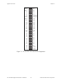
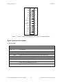
Figure 3-1 shows the pin assignments for the PC-AO-2DC I/O connector. You can use the
CB-50 LP or CB-50 I/O connector block and the NB1 cable with the PC-AO-2DC for your
prototyping needs.
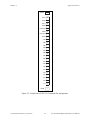
Figure 3-2 shows the pin assignments for the DAQCard-AO-2DC I/O connector. This connector
is located on the edge of the DAQCard-AO-2DC and is accessible at the slot opening of your
computer after the card has been properly installed.
Figure 3-3 shows the screw terminal assignments for the CB-27 accessory when connected to the
DAQCard-AO-2DC using the PR27-30F ribbon cable.
© National Instruments Corporation
3-1
PC-AO-2DC/DAQCard-AO-2DC User Manual
Signal Connections
Chapter 3
IOUT0
1
2
NC
IOUT1
3
4
NC
NC
5
6
NC
NC
7
8
NC
NC
9
10
DAC0OUT
AGND
11 12
DAC1OUT
DGND
13 14
PA0
PA1
15 16
PA2
PA3
17 18
PA4
PA5
19 20
PA6
PA7
21 22
PB0
PB1
23 24
PB2
PB3
25 26
PB4
PB5
27 28
PB6
PB7
29 30
NC
NC
31 32
NC
NC
33 34
NC
NC
35 36
NC
NC
37 38
NC
NC
39 40
NC
NC
41 42
NC
NC
43 44
NC
NC
45 46
NC
NC
47 48
DGND
+5 V
49 50
DGND
Figure 3-1. PC-AO-2DC I/O Connector Pin Assignments
PC-AO-2DC/DAQCard-AO-2DC User Manual
3-2
© National Instruments Corporation
Chapter 3
Signal Connections
SHIELD
27
IOUT0
26
AGND
25
IOUT1
24
AGND
23
DAC0OUT
22
AGND
21
DAC1OUT
20
AGND
19
PB7
18
PB6
17
PB5
16
PB4
15
PB3
14
PB2
13
PB1
12
PB0
11
PA7
10
PA6
9
PA5
8
PA4
7
PA3
6
PA2
5
PA1
4
PA0
3
+5 V
2
DGND
1
Figure 3-2. DAQCard-AO-2DC I/O Connector Pin Assignments
© National Instruments Corporation
3-3
PC-AO-2DC/DAQCard-AO-2DC User Manual
Signal Connections
Chapter 3
PB3
14
1
DGND
PB4
15
1
DGND
PB5
16
2
+5 V
PB6
17
3
PA0
PB7
18
4
PA1
AGND
19
5
PA2
DAC1OUT
20
6
PA3
AGND
21
7
PA4
DAC0OUT
22
8
PA5
AGND
23
9
PA6
IOUT1
24
10
PA7
AGND
25
11
PB0
IOUT0
26
12
PB1
SHIELD
27
13
PB2
Figure 3-3. Screw Terminal Assignments for the CB-27 I/O Connector Block
Signal Connection Descriptions
♦ PC-AO-2DC
Pin
1
2, 4–9,
30–48
3
10
11
12
13, 50
14–21
Signal Name Description
IOUT0
Current Out 0—This signal is the current output for channel 0.
NC
Not connected.
22–29
PB<0..7>
49
+5 V
IOUT1
DAC0OUT
AGND
DAC1OUT
DGND
PA<0..7>
Current Out 1—This signal is the current output for channel 1.
DAC0 Out—This signal is the voltage output for channel 0.
Analog Ground—This is the ground reference for analog output signals.
DAC1 Out—This is the voltage output signal for channel 1.
Digital Ground—This is the ground reference for digital output/input signals.
Port A0 through Port A7—These signals are the bidirectional digital data lines for
port A. PA7 is the MSB; PA0 is the LSB.
Port B0 through Port B7—These signals are the bidirectional digital data lines for
port B. PB7 is the MSB; PB0 is the LSB.
+5 V—This output signal carries 1 A maximum. This has an internal resettable
fuse.
PC-AO-2DC/DAQCard-AO-2DC User Manual
3-4
© National Instruments Corporation
Chapter 3
Signal Connections
♦ DAQCard-AO-2DC
Pin
1
2
3–10
11–18
19, 21,
23, 25
20
22
24
26
27
Signal Name Description
DGND
Ground—This pin is connected to the computer ground and digital ground signals.
+5V
+5 V—This output signal carries 500 mA maximum and has an internal nonresettable wire fuse.*
PA<0..7>
Port A0 through Port A7—These signals are bidirectional digital data lines for
port A. PA7 is the MSB; PA0 is the LSB.
PB<0..7>
Port B0 through Port B7—These signals are bidirectional digital data lines for
port B. PB7 is the MSB; PB0 is the LSB.
AGND
Analog Ground—This is the ground reference for analog output signals.
DAC1OUT
DAC0OUT
IOUT1
IOUT0
SHIELD
DAC1 Out—This is the voltage output signal for channel 1.
DAC0 Out—This is the voltage output signal for channel 0.
Current Out for Channel 1—This signal is the current output for channel 1.
Current Out for Channel 0—This signal is the current output for channel 0.
Shield—This pin is connected to the card shield and computer ground.
* The DAQCard-AO-2DC fuse is a non-resettable 500 mA, 32 V, fast-acting fuse
manufactured by Little Fuse (part number LIT 418.500).
You can use the CB-27 I/O connector block and the PR27-30F cable with the
DAQCard-AO-2DC for your prototyping needs.
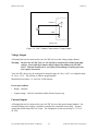
Analog Output Signal Connections
The PC-AO-2DC uses pins 1, 3, and 10–12 for analog output. The DAQCard-AO-2DC uses
pins 20–26 for analog output. The DAQCard-AO-2DC provides individual grounds for each
current/voltage output. You can connect each AO-2DC output channel independently for either
voltage output or current output. Figure 3-4 shows how to make these signal connections.
© National Instruments Corporation
3-5
PC-AO-2DC/DAQCard-AO-2DC User Manual
Signal Connections
Chapter 3
AO-2DC
DACxOUT
Load
AGND
A
Floating Load
Figure 3-4. DAC Channel Connection as Voltage Output
Voltage Output
A floating load may be connected to your AO-2DC device at the voltage output channel.
Warning: Because the AO-2DC device is not optically or magnetically isolated from high
voltages, a load with high common mode voltages may damage the AO-2DC
device. National Instruments is NOT liable for any damages resulting from any
such signal connections.
Your AO-2DC device may be configured in unipolar range of 0.0 to +10.0 V or in bipolar range
of -5.0 to +5.0 V. The polarity is software programmable.
Maximum load current = ±1.0 mA for 12-bit linearity
Power-up Condition
•
Range: Unipolar
•
Output voltage: ±500 mV maximum within 100 ms of power up
Current Output
A floating load may be connected to your AO-2DC device at the current output channel. An
external floating power supply is needed to complete the controlled current loop. You may
control the current loop from 0 to 20 mA. The compliance for the current loop is +7.0 V to
40 VDC.
PC-AO-2DC/DAQCard-AO-2DC User Manual
3-6
© National Instruments Corporation
Chapter 3
Signal Connections
Warning: Because the AO-2DC device is not optically or magnetically isolated from high
voltages, a load with high common mode voltages may damage the AO-2DC
device. National Instruments is NOT liable for any damages resulting from any
such signal connections.
Your AO-2DC device has to be configured in unipolar range of 0.0 to +10.0 V for the current
outputs to function correctly. When you use an external supply, the order of the supply and load
does not matter as long as you do not create a second loop through which current flows.
•
External loop supply voltage: +7.0 V to +40.0 VDC
Power-up Condition
•
Range: Unipolar
•
Output current: 0 mA
Figure 3-5 shows how to connect a DAC channel as a current output using an external loop
supply.
PC-AO-2DC or
DAQCard-AO-2DC
IOUTx
Load
Vext +
-
0-20 mA
PC-AO-2DC or
DAQCard-AO-2DC
IOUTx
0-20 mA
OR
Vext +
AGND
Load
AGND
A
a. Floating Load
A
b. Floating Supply
Figure 3-5. DAC Channel Connection as Current Output, External Loop Supply
Figure 3-6 shows an example of a circuit with a second loop; this circuit does not work.
© National Instruments Corporation
3-7
PC-AO-2DC/DAQCard-AO-2DC User Manual
Signal Connections
Chapter 3
Vext
PC-AO-2DC or
DAQCard-AO-2DC
+
Uncontrolled
Loop Control
Load
IOUTx
AGND
A
Figure 3-6. Current Loop Connection, Load and External Supply Grounded
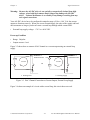
Digital I/O Signal Connections
The PC-AO-2DC uses pins 13–29 and pin 50 for digital I/O; the DAQCard-AO-2DC uses
pins 1–18 for digital I/O. Figure 3-7 illustrates signal connections for three typical digital I/O
applications.
+5 V
LED
Port A
PA0
PA<7..0>
R
PB0
TTL Signal
+5 V
Port B
PB1
PB<7..0>
Switch
DGND
I/O Connector
PC-AO-2DC or DAQCard-AO-2DC
Figure 3-7. Digital I/O Connections
In Figure 3-7, port A is configured for digital output and port B is configured for digital input.
PC-AO-2DC/DAQCard-AO-2DC User Manual
3-8
© National Instruments Corporation
Chapter 3
Signal Connections
Digital input applications include receiving TTL signals and sensing external device states such
as the switch in Figure 3-7. Digital output applications include sending TTL signals and driving
external devices such as the LED shown in Figure 3-7.
Refer to Appendix A, Specifications, for a list of the digital I/O signal ratings.
Power-up Condition
At power up, both port A and port B of the digital I/O circuitry on the PC-AO-2DC and
DAQCard-AO-2DC are configured as input ports. Also, these ports have weak internal pull ups.
© National Instruments Corporation
3-9
PC-AO-2DC/DAQCard-AO-2DC User Manual
Chapter 4
Theory of Operation
This chapter describes the theory of operation for analog output and digital I/O using the
PC-AO-2DC and DAQCard-AO-2DC.
Functional Overview
The block diagram in Figure 4-1 shows a functional overview of the PC-AO-2DC and
DAQCard-AO-2DC.
82C55A
Digital
I/O
Data/
Address
PB
12-Bit DAC
DAC0OUT
Control
DAC1OUT
Control
12-Bit DAC
Address
Select and
Control
Back Panel Connector
PC I/O Channel PC/PCMCIA* I/O
PC/PCMCIA*
I/O Channel
Interface
PA
IOUT0
Current
Outputs
IOUT1
1 A Resettable Fuse (PC)
+5 V
500 mA Non-resettable Fuse (PCMCIA)
Figure 4-1. PC-AO-2DC and DAQCard-AO-2DC Block Diagram
*
PC I/O Channel for PC-AO-2DC; PCMCIA I/O Channel for DAQCard-AO-2DC
© National Instruments Corporation
4-1
PC-AO-2DC/DAQCard-AO-2DC User Manual
Theory of Operation
Chapter 4
Your AO-2DC device consists of the following major components:
•
I/O channel interface circuitry
•
Analog output circuitry
•
Digital I/O circuitry
You can execute data acquisition functions by using the analog output circuitry and the digital
I/O circuitry, which are described in detail in the Analog Output and Digital I/O sections later in
this chapter. The internal data and control buses interconnect the components.
I/O Channel Interface Circuitry
The I/O channel interface circuitry consists of address decoders, data buffers, and I/O channel
interface timing control circuitry. The circuitry monitors the address lines and timing signals to
generate the device select, register select, control, and read/write signals. The data buffers
provide larger drive and control the direction of data transfer on the bidirectional data lines based
on whether the transfer is a read or write.
♦ PC-AO-2DC
The PC I/O channel of the PC-AO-2DC consists of an address bus, a data bus, and several
control and support signals. The components making up the PC I/O channel interface
circuitry is shown in Figure 4-2.
PC I/O Channel
Address Bus
Plug and
Play Control
Timing
Interface
Control Lines
Data Bus
8
Address
Decoder
Data
Buffers
Register Selects
Control and
Read/Write Signals
Internal Data Bus
Figure 4-2. PC I/O Interface Circuitry Block Diagram of PC-AO-2DC
PC-AO-2DC/DAQCard-AO-2DC User Manual
4-2
© National Instruments Corporation
Chapter 4
Theory of Operation
♦ DAQCard-AO-2DC
The PCMCIA I/O channel of the DAQCard-AO-2DC consists of an address bus, a data bus,
and several control and support signals. The components making up the PCMCIA I/O
channel interface circuitry are shown in Figure 4-3.
PC I/O ChannelPCMCIA Channel
Control Lines
Timing
Interface
Control and
Read/Write Signals
Address Bus
Address
Decoder
Card
Information
Structure
Data Bus
8
Register Selects
Data
Buffers
PCMCIA
Control
Registers
Internal Data Bus
Figure 4-3. PCMCIA I/O Interface Circuitry Block Diagram of DAQCard-AO-2DC
Analog Output
Analog outputs supported by the PC-AO-2DC and DAQCard-AO-2DC consist of two channels
of voltage or current output. The theory of operation and signal connections of the analog output
circuitry are described in this section.
Your AO-2DC device provides two channels of analog output through two 12-bit DACs. Each
analog output channel can provide a unipolar or bipolar voltage output or current output.
Figure 4-4 shows a block diagram of the analog output circuitry.
© National Instruments Corporation
4-3
PC-AO-2DC/DAQCard-AO-2DC User Manual
Theory of Operation
Chapter 4
Current
Output
IOUT0
DAC0WR
DAC0OUT
DAC0
5 V Internal
Reference
Data
AGND
I/O Connector
PC I/O Channel
PCMCIA Channel
Ref
PC/PCMCIA
I/O Channel
Interface and
Control
Ref
DAC1
DAC1OUT
DAC1WR
Current
Output
IOUT1
Figure 4-4. Analog Output Circuitry Block Diagram
Each analog output channel contains a 12-bit DAC and voltage-to-current conversion circuitry.
Each DAC channel can be software-configured for either a unipolar voltage output or a bipolar
voltage output range. A unipolar output gives an output voltage range of 0.0 to +10.0 V. A
bipolar output gives an output voltage range of -5.0 to +5.0 V. You can generate the desired
voltage using applicable NI-DAQ function calls. For the proper connection for voltage output,
refer to Chapter 3, Signal Connections.
Each DAC channel can be software-configured for current outputs. The voltage-to-current
conversion circuitry of each analog output channel can create a 0 to 20 mA current sink using an
external current loop supply of 7 to 40 V. The current sink converts the voltage from the output
of DACs. For the current sink to operate properly, you must use the unipolar voltage output
mode. You can use the current output with industry standard 0 to 20 mA or 4 to 20 mA current
loops. You can generate the desired current loop using applicable NI-DAQ function calls. For
proper connections for current outputs, refer to Chapter 3, Signal Connections.
PC-AO-2DC/DAQCard-AO-2DC User Manual
4-4
© National Instruments Corporation
Chapter 4
Theory of Operation
Digital I/O
Your AO-2DC device supports 16-bit digital I/O. The 16 bits are configured as two 8-bit ports
that can each be used either as an input port or an output port.
The digital I/O circuitry is designed around the 82C55A general-purpose programmable
peripheral interface (PPI). Two of the ports, port A and port B, are used in the AO-2DC devices.
The pins that correspond to these ports are PA<0..7> and PB<0..7> on the AO-2DC connectors.
Figure 4-5 shows a block diagram of the digital I/O circuitry. For performing and configuring
digital I/O operations, use applicable NI-DAQ function calls.
PCMCIA Channel
DATA <0..7>
82C55A
Programmable
Peripheral
Interface
8
PB <0..7>
I/O Connector
PA <0..7>
Address <0..1>
8
Control
Figure 4-5. Digital I/O Circuitry Block Diagram
All ports on the 82C55A are TTL-compatible. When enabled, the digital output ports are
capable of sinking 2.5 mA of current and sourcing 2.5 mA of current on each digital I/O line.
When the ports are not enabled, the digital I/O lines act as high-impedance inputs, which have
been pulled up by weak pull-up resistors.
© National Instruments Corporation
4-5
PC-AO-2DC/DAQCard-AO-2DC User Manual
Theory of Operation
Chapter 4
Power-down Mode
DAQCard-AO-2DC only
You can power down your DAQCard-AO-2DC by using the power-down utility provided
with your NI-DAQ software. This utility will put your DAQCard-AO-2DC in a low-power
consumption mode. The effects of power-down mode are as follows:
•
The analog output values will not be maintained. For example, if you have set up your
voltage output channel to unipolar mode and you are outputting +9.000 V, then after
power-down mode the output levels will fall to an unknown level.
•
The digital I/O will not be functional.
•
After you bring your DAQCard-AO-2DC back from power-down mode to power-up
mode, you are required to set up your analog outputs again.
If you are using a PC, bring your DAQCard-AO-2DC to power-down mode by typing:
daqpower D and to power-up your DAQCard-AO-2DC again, type: daqpower U.
If you are using a Mac, refer to your NI-DAQ for Macintosh documentation to use the
power-down utilities for PCMCIA cards.
Refer to the configuration utility online documentation that is shipped with your PCMCIA card
for more information on power-down features.
PC-AO-2DC/DAQCard-AO-2DC User Manual
4-6
© National Instruments Corporation
Appendix A
Specifications
This appendix lists the specifications of the PC-AO-2DC and DAQCard-AO-2DC. These specifications are typical
at 25° C and 50% relative humidity unless otherwise stated.
Analog Output
Output Characteristics
Number of channels ................................................................... Two voltage and two current
Resolution................................................................................... 12 bits
Type of DAC ..............................................................................Double buffered
Data transfers ............................................................................. Programmed I/O
Transfer Characteristics
Relative accuracy (INL) of the DAC ......................................... ±0.5 LSB max 1
DNL ........................................................................................... ±1 LSB max
Monotonicity ..............................................................................Guaranteed over temperature
Voltage Output
Ranges ........................................................................................0 to 10 VDC, ±5 V, software selectable
Output coupling..........................................................................DC
Output impedance ......................................................................0.5 Ω
Current drive ..............................................................................±2.0 mA max2
Absolute accuracy ......................................................................0.05% FSR3
Protection ................................................................................... Short circuit to ground
Power-on state ............................................................................±500 mV within 100 ms, unipolar mode4
Current Output
Range ......................................................................................... 0 to 20 mA
Type ........................................................................................... Sink to GND, requires external current loop supply
Output impedance ......................................................................1 GΩ
Excitation voltage range............................................................. +7 to +40 VDC
Absolute accuracy ......................................................................0.15% FSR
Protection ................................................................................... Short circuit to ground
Power-on state ............................................................................0 A within 100 ms4
1
2
3
4
The relative accuracy for the software corrected DAC is ±1.53 LSB max.
This limit is for the ±5 V range. For unipolar 0–10 VDC range, the current drive is ±1 mA max.
The FSR for either unipolar or bipolar mode is 10 V.
The output level is unknown in the first 100 ms after power up.
© National Instruments Corporation
A-1
PC-AO-2DC/DAQCard-AO-2DC User Manual
Specifications
Appendix A
Dynamic Characteristics
Settling time ..............................................................................100 µs 0 to 10 VDC
70 µs -5 to +5 VDC
Slew rate..................................................................................... 0.30 V/µs
Noise........................................................................................... 45 µVrms, 0 to 22 kHz
Stability
Recommended warm-up time ....................................................15 minutes
Offset temperature coefficient....................................................-60 µV/°C
Gain temperature coefficient ......................................................±26 ppm/°C
Digital I/O
Number of channels ................................................................... 16 digital I/O available as two 8-bit ports
Compatibility ............................................................................. TTL
Power-on state ............................................................................Configured as inputs and internally pulled up
Digital logic levels .....................................................................
Level
Min
Max
Input low voltage
Input high voltage
Input leak current
(0 < Vin < 5 V)
Output low voltage
(Iout = 2.5 mA)
Output high voltage
(Iout = 2.5 mA)
-0.3 V
2.2 V
0.8 V
5.0 V
-1.0 µA
1 µA
0.0 V
0.4 V
3.7 V
5.0 V
Transfer rate (1 word = 8 bits)5
Input ........................................................................................... 1 MHz max
Output......................................................................................... 1 MHz max
Bus Interface
Type ........................................................................................... Slave
Power Requirements
♦
5
PC-AO-2DC
+5 VDC (±5%)....................................................................350 mA max
+12 VDC (±5%)................................................................. 30 mA max
-12 VDC (±5%) ................................................................. 30 mA max
These limits on the transfer rates are set by the digital I/O circuitry on the card. Actual transfer rates may be
lower than these limits, depending on the type of computer, CPU speed, operating system, and the software used.
PC-AO-2DC/DAQCard-AO-2DC User Manual
A-2
© National Instruments Corporation
Appendix A
♦
Specifications
DAQCard-AO-2DC
+5 VDC (±5%)....................................................................89 mA typ
95 mA max
26 mA power-down mode
Note: These specifications do not include power consumed by devices connected to the fused
+5 V supply pin on the I/O connector.
Physical
♦
PC-AO-2DC
Dimensions ......................................................................... 11.3 by 9.9 cm (4.45 by 3.90 in.)
I/O connector....................................................................... 50-pin male
♦
DAQCard-AO-2DC
PCMCIA card type ............................................................. Type II
I/O connector....................................................................... 25-pin female PCMCIA I/O connector on card
Environment
Operating ....................................................................................0° to 50° C
Temperature ............................................................................... -55° to 125° C
Relative humidity ....................................................................... 5% to 90% noncondensing
© National Instruments Corporation
A-3
PC-AO-2DC/DAQCard-AO-2DC User Manual
Appendix B
X25020 Data Sheet*
This appendix contains a manufacturer data sheet for the X25020 SPI serial EEPROM (Xicor).
This EEPROM is used on both the PC-AO-2DC and the DAQCard-AO-2DC.
* Copyright © Xicor. 1995. Reprinted with permission of copyright owner. All rights reserved.
Xicor, Inc. 1995 Data Book.
© National Instruments Corporation
B-1
PC-AO-2DC/DAQCard-AO-2DC User Manual
Appendix C
Connector Block Pin Map
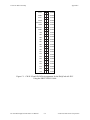
This appendix gives the pin assignments for the CB-50 LP or CB-50 I/O connector blocks when
using the PSH27-50F-D1 with the DAQCard-AO-2DC.
If you are using the CB-50 LP or CB-50 I/O connector block and the PSH27-50F-D1 cable with
the DAQCard-AO-2DC, the signals will not map at the same pin numbers as the pin numbers
shown for the CB-50 I/O connector block for the PC-AO-2DC. For these pin numbers refer to
Figure C-1.
Note:
Using the PSH27-50F-D1 cable with the DAQCard-AO-2DC is not recommended
because the PSH27-50F-D1 design is optimized for the DAQCard-DIO-24.
© National Instruments Corporation
C-1
PC-AO-2DC/DAQCard-AO-2DC User Manual
Connector Block Pin Map
Appendix C
IOUT0
1
2
DGND
AGND
3
4
DGND
IOUT1
5
6
DGND
AGND
7
8
DGND
DAC0OUT
9
10
DGND
AGND
11 12
DGND
DAC1OUT
13 14
DGND
AGND
15 16
DGND
PB7
17 18
DGND
PB6
19 20
DGND
PB5
21 22
DGND
PB4
23 24
DGND
PB3
25 26
DGND
PB2
27 28
DGND
PB1
29 30
DGND
PB0
31 32
DGND
PA7
33 34
DGND
PA6
35 36
DGND
PA5
37 38
DGND
PA4
39 40
DGND
PA3
41 42
DGND
PA2
43 44
DGND
PA1
45 46
DGND
PA0
47 48
DGND
+5 V
49 50
DGND
Figure C-1. CB-50 LP and CB-50 Pin Assignments for the DAQCard-AO-2DC
Using the PSH27-50F-D1 Cable
PC-AO-2DC/DAQCard-AO-2DC User Manual
C-2
© National Instruments Corporation
Appendix D
Register-Level Programming
This document describes in detail the address and function of each of the PC-AO-2DC and
DAQCard-AO-2DC registers.
Note:
If you plan to use a programming software package such as NI-DAQ or
LabWindows/CVI with your PC-AO-2DC and DAQCard-AO-2DC, you need not read
this chapter.
Base I/O Address Selection
♦ PC-AO-2DC
You can configure your PC-AO-2DC board to use base addresses in the range of 100 to 3E0
hex. Your PC-AO-2DC board occupies 32 bytes of address space and must be located on a
32-byte boundary. Therefore, valid addresses include 100, 120, 140, ..., 3C0, 3E0 hex. This
selection is software configured and does not require you to manually change any settings on
the board.
The PC-AO-2DC board is fully compatible with the industry standard Intel-Microsoft Plug
and Play Specification version 1.0a. A Plug and Play system arbitrates and assigns resources
through software, freeing you from manually setting switches and jumpers.
There are different ways of assigning the base address to your board:
•
Windows 95 automatically assigns the base address.
•
You can use a standard configuration utility like Intel ISA Configuration Utility (ICU).
ICU dynamically assigns the base address to your board when you boot up the computer.
You can also lock the board resources when you use ICU. For additional information on
ICU, contact Intel Corporation for a copy of Plug and Play Specification version 1.0a.
•
You can use DAQCONF or WDAQCONF to assign the board resources. If a standard
configuration utility is present in the system, you will not be able to modify the board
resources.
© National Instruments Corporation
D-1
PC-AO-2DC/DAQCard-AO-2DC User Manual
Register-Level Programming
Appendix D
♦ DAQCard-AO-2DC
•
If you are using a PC, you can use Windows 95, DAQCONF, or WDAQCONF to assign the
device resources. If a standard configuration utility is present in the system, you will not
be able to modify the device resources. Consult the document, PCMCIA Card and
Socket Services Specifications, which explains how to configure a card using systemlevel calls. Request an I/O window, an interrupt level, and a configuration. In the
configuration, set the configuration index to 01 hex for normal operation.
•
If you are using a Mac, refer to your NI-DAQ for Macintosh documentation for PCMCIA
card configuration information. Consult the document, PCMCIA Card and Socket
Services Specifications, which explains how to configure a card using system-level calls,
and the PC Card Development Kit (available from Apple through APDA), which
explains how to interface with the Apple PC Card Manager software that is part of your
PC Card expansion interface. Request a configuration and an I/O window. In the
configuration, set the configuration index to 01 hex for normal operation.
Register Map
Table D-1 gives the register map for the PC-AO-2DC and DAQCard-AO-2DC.
Table D-1. PC-AO-2DC and DAQCard-AO-2DC Register Map
Register Name
Offset Address
(Hex)
Type
Size
Configuration and Calibration Register Group
Command Register 1
Command Register 2
Calibration Command Register 3
Calibration EEPROM Register
01
0E
1C
1D
Write-only
Write-only
Write-only
Read-only
8-bit
8-bit
8-bit
8-bit
Analog Output Register Group
DAC0 Low-Byte Register
DAC0 High-Byte Register
DAC1 Low-Byte Register
DAC1 High-Byte Register
04
05
06
07
Write-only
Write-only
Write-only
Write-only
8-bit
8-bit
8-bit
8-bit
82C55A Digital I/O Register Group
Port A Register
Port B Register
Digital Control Register
10
11
13
Read-and-write
Read-and-write
Write-only
8-bit
8-bit
8-bit
PC-AO-2DC/DAQCard-AO-2DC User Manual
D-2
© National Instruments Corporation
Appendix D
Register-Level Programming
Register Description
Table D-1 divides the PC-AO-2DC and DAQCard-AO-2DC registers into three different register
groups. A bit description of each register is included later in this chapter. The Configuration
and Calibration Register Group controls the overall operation of the PC-AO-2DC or
DAQCard-AO-2DC. The Analog Output Register Group accesses the two 12-bit DACs. The
Digital I/O Register Group consists of the three registers of the onboard 82C55A PPI integrated
circuit used for digital I/O.
Register Description Format
The remainder of this chapter discusses each of the PC-AO-2DC and DAQCard-AO-2DC
registers in the order shown in Table D-1. Each register group section begins with a brief
introduction, followed by a detailed bit description of each register on the AO-2DC devices.
Each register description gives the address, type, word size, and bit map of the register, followed
by a description of each bit.
The register bit map shows a diagram of the register with the MSB (bit 7 for an 8-bit register)
shown on the left, and the LSB (bit 0) shown on the right. Each bit is represented by a square
with the bit name inside. An asterisk (*) after the bit name indicates that the bit is inverted
(negative logic). An X represents a don’t care state; in other words, the logic may be digital
0 or 1 and this bit should be ignored.
© National Instruments Corporation
D-3
PC-AO-2DC/DAQCard-AO-2DC User Manual
Register-Level Programming
Appendix D
Configuration and Calibration Register Group
The four registers making up the Configuration and Calibration Register Group allow general
control of the PC-AO-2DC and DAQCard-AO-2DC D/A circuitry. Command Register 1 and
Command Register 2 contain bits that control the operation modes of the D/A circuitry.
Command Register 3 is for writing to the EEPROM. The EEPROM Register gives access to the
EEPROM. When you start up your PC, all bits of the Command Registers are cleared except
Command Register 2, where bits 2 and 3 are set during power up.
Bit descriptions for the registers in the Configuration and Calibration Register Group are given
on the following pages.
Command Register 1
Command Register 1 contains two bits that control PC-AO-2DC and DAQCard-AO-2DC analog
output modes.
Address:
Base address + 01 (hex)
Type:
Write-only
Word Size:
8-bit
Bit Map:
7
6
5
4
3
2
1
0
0
0
2SDAC1
2SDAC0
0
0
0
0
Bit
Name
Description
7, 6,
3–0
0
Write zeroes to these bits.
5
2SDAC1
Two’s complement DAC1—This bit selects the binary coding
scheme used for the DAC1 data. If this bit is set, a two's
complement binary coding scheme is used for interpreting the
12-bit data. Two's complement is useful if a bipolar output range
is selected. If this bit is cleared, a straight binary coding scheme is
used. Straight binary is useful if a unipolar output range is
selected.
4
2SDAC0
Two’s complement DAC0—This bit selects the binary coding
scheme used for the DAC0 data. If this bit is set, a two's
complement binary coding scheme is used for interpreting the
12-bit data. Two's complement is useful if a bipolar output range
is selected. If this bit is cleared, a straight binary coding scheme is
used. Straight binary is useful if a unipolar output range is
selected.
PC-AO-2DC/DAQCard-AO-2DC User Manual
D-4
© National Instruments Corporation
Appendix D
Register-Level Programming
Command Register 2
Command Register 2 configures the D/A circuitry.
Address:
Base address + 0E (hex)
Type:
Write-only
Word Size:
8-bit
Bit Map:
7
6
5
4
3
2
1
0
0
0
0
0
DAC1UNI/BI*
DAC0UNI/BI*
0
0
Bit
Name
Description
7–4,
0
Write zeroes to these bits.
3
DAC1UNI/BI*
DAC1 Unipolar/Bipolar—This bit sets the analog voltage output
range for DAC1. Set this bit to configure DAC1 for a unipolar
(0 to +10 V) output voltage range. Clear this bit to configure
DAC1 for bipolar (-5 to +5 V) output voltage range.
2
DAC0UNI/BI*
DAC0 Unipolar/Bipolar—This bit sets the analog voltage output
range for DAC0. Set this bit to configure DAC0 for a unipolar
(0 to +10 V) output voltage range. Clear this bit to configure
DAC0 for bipolar (-5 to +5 V) output voltage range.
Note: At power up, both the DACs are configured for unipolar output voltage range.
© National Instruments Corporation
D-5
PC-AO-2DC/DAQCard-AO-2DC User Manual
Register-Level Programming
Appendix D
Command Register 3
This register is used to write to the onboard Calibration EEPROM.
Address:
Base address + 1C (hex)
Type:
Write-only
Word Size:
8-bit
Bit Map:
7
6
5
4
3
2
1
0
EEPROMCS
SDATA
SCLK
0
0
WRTPRT
0
0
Bit
Name
Description
7
EEPROMCS
EEPROM Chip Select—This bit enables and disables the
EEPROM. You can enable the EEPROM for both read and write
operations by setting this bit. You can disable the EEPROM by
clearing this bit.
6
SDATA
Serial Data—This bit is a serial input for the calibration EEPROM.
5
SCLK
Serial Clock—This bit is a serial clock for the calibration
EEPROM. A low-to-high transition of this bit clocks data into the
EEPROM (during a write operation). A high-to-low transition of
the bit clocks data out of the EEPROM (during a read operation).
4, 3,
1, 0
0
Write zeroes to these bits.
2
WRTPRT
Write Protect—This bit controls the write protect input signal for
the EEPROM. When you set this bit, normal write operations are
enabled. When you clear this bit, write operations are disabled.
Note: To program the X25020 EEPROM, refer to the data sheets in Appendix B, X25020
Data Sheet.
PC-AO-2DC/DAQCard-AO-2DC User Manual
D-6
© National Instruments Corporation
Appendix D
Register-Level Programming
Calibration EEPROM Register
The Calibration EEPROM Register gives access to the output of the EEPROM.
Address:
Base address + 1D (hex)
Type:
Read-only
Word Size:
8-bit
Bit Map:
7
6
5
4
3
2
1
0
X
X
X
X
X
X
X
PROMOUT
Bit
Name
Description
7–1
X
Don’t care bit—You can mask these bits when reading the
EEPROM.
0
PROMOUT
EEPROM Output—This bit allows access to the serial output pin
of the EEPROM. During calibration procedures, the calibration
data is read from the EEPROM through PROMOUT.
Note: To program the X25020 EEPROM, refer to the data sheets in Appendix B, X25020
Data Sheet.
Analog Output Register Group
The four registers making up the Analog Output Register Group are used for loading the two
12-bit DACs in the two analog output channels. DAC0 controls analog output Channel 0.
DAC1 controls analog output channel 1. These DACs should be written to individually.
The DAC in each analog output channel generates a voltage proportional to the input Vref
multiplied by the digital code loaded into the DAC. The DACs have an 8-bit loading interface.
Each DAC can be loaded with a 12-bit digital code by writing first to the low byte and then to
the high byte. The voltage outputs from the two DACs are updated at the PC-AO-2DC or
DAQCard-AO-2DC I/O connector at the DAC0OUT and DAC1OUT pins as soon as the high
byte is written to the DACx registers.
Bit descriptions of the registers making up the Analog Output Register Group are given on the
following page.
© National Instruments Corporation
D-7
PC-AO-2DC/DAQCard-AO-2DC User Manual
Register-Level Programming
Appendix D
Programming the Analog Outputs
Voltage Outputs
Use the pseudocode for generating a desired voltage at the output of a channel or refer to the
Programming Example section later in this appendix:
1. Write to the Command Register 1 to select the binary coding scheme to be used for DAC
data. You can choose the two’s complement scheme for bipolar outputs and straight binary
is used for unipolar output.
2. Select the polarity of the DAC by writing to Command Register 2. This will select unipolar
output or bipolar output.
Note: Power-up default is unipolar output on both channels.
3. Perform calibration if desired. Refer to Appendix E, Calibration, for more information. You
will have to write to Calibration Command Register 3 to write to the EEPROM.
4. Read the calibration coefficients and calculate the binary pattern to be written to the DAC to
generate the desired voltage output.
Note: Refer to Appendix E, Calibration, to find the formula to calculate digital value to be
written to DAC for a desired voltage.
5. Write the LSB of the digital value to the DAC0L/DAC1L and then write the MSB of the
digital value to the DAC0H/DAC1H. When you finish writing to DACxH, the output will be
updated.
Current Outputs
The pseudocode is identical to that for voltage outputs except Step 2, where the unipolar range
should always be selected for current outputs.
PC-AO-2DC/DAQCard-AO-2DC User Manual
D-8
© National Instruments Corporation
Appendix D
Register-Level Programming
DAC0 Low-Byte (DAC0L), DAC0 High-Byte (DAC0H), DAC1 Low-Byte (DAC1L), and
DAC1 High-Byte (DAC1H) Registers
Writing to DAC0L and then to DAC0H loads the analog output channel 0. Writing to DAC1L
and then to DAC1H loads the analog output channel 1. The voltage generated by both of the
analog output channels is updated immediately after either DACxH register is written to.
Address:
Base address + 04 (hex)
Base address + 05 (hex)
Base address + 06 (hex)
Base address + 07 (hex)
Type:
Write-only (all)
Word Size:
8-bit (all)
Load DAC0 low byte.
Load DAC0 high byte.
Load DAC1 low byte.
Load DAC1 high byte.
Bit Map:
DACxH
7
6
5
4
3
2
1
0
D15
D14
D13
D12
D11
D10
D9
D8
{––––––––––––––Sign Extension Bits––––––––––––––}
DACxL
7
6
5
4
3
2
1
0
D7
D6
D5
D4
D3
D2
D1
D0
Bit
Name
Description
7–4
D<15..12>
Data bits 15 through 12—These bits are set to zero in straight
binary mode and to sign extension in two's complement mode.
3–0
D<11..8>
Data bits 11 through 8—These four bits are loaded into the
specified DAC high byte.
D<7..0>
Data bits 7 through 0—These eight bits are loaded into the
specified DAC low byte. The low byte should be loaded first,
followed by corresponding high byte loading.
DACxH
DACxL
7–0
© National Instruments Corporation
D-9
PC-AO-2DC/DAQCard-AO-2DC User Manual
Register-Level Programming
Appendix D
82C55A Digital I/O Register Group
Digital I/O on the PC-AO-2DC and DAQCard-AO-2DC uses an 82C55A integrated circuit. The
82C55A is a general-purpose programmable peripheral interface (PPI). Two ports, port A and
port B, are used in the PC-AO-2DC and DAQCard-AO-2DC. These ports are programmed as
two groups of eight signals for either input or output.
Bit descriptions for the registers in the Digital I/O Register Group are given on the following
pages.
Note: Interrupts are not supported on PC-AO-2DC or DAQCard-AO-2DC.
Port A Register
Reading the Port A Register returns the logic state of the eight digital I/O lines constituting
port A, that is, PA<0..7>. If port A is configured for output, the Port A Register can be written
to in order to control the eight digital I/O lines constituting port A. See Programming the Digital
I/O Circuitry later in this appendix for information on how to configure port A for input or
output.
Address:
Base address + 10 (hex)
Type:
Read-and-write
Word Size:
8-bit
Bit Map:
7
6
5
4
3
2
1
0
D7
D6
D5
D4
D3
D2
D1
D0
Bit
Name
Description
7–0
D<7..0>
Data bits 7 through 0—These bits are 8-bit port A data.
PC-AO-2DC/DAQCard-AO-2DC User Manual
D-10
© National Instruments Corporation
Appendix D
Register-Level Programming
Port B Register
Reading the Port B Register returns the logic state of the eight digital I/O lines constituting port
B, that is, PB<0..7>. If port B is configured for output, the Port B Register can be written to in
order to control the eight digital I/O lines constituting port B. See Programming the Digital I/O
Circuitry later in this appendix for information on how to configure port B for input or output.
Address:
Base address + 11 (hex)
Type:
Read-and-write
Word Size:
8-bit
Bit Map:
7
6
5
4
3
2
1
0
D7
D6
D5
D4
D3
D2
D1
D0
Bit
Name
Description
7–0
D<7..0>
Data bits 7 through 0—These bits are 8-bit port B data.
Digital Control Register
The Digital Control Register can be used to configure port A and port B as inputs or outputs.
See Programming the Digital I/O Circuitry later in this appendix for a description of the
individual bits in the Digital Control Register.
Address:
Base address + 13 (hex)
Type:
Write-only
Word Size:
8-bit
Bit Map:
7
6
5
4
3
2
1
0
CW7
CW6
CW5
CW4
CW3
CW2
CW1
CW0
Bit
Name
Description
7–0
CW<7..0>
Control Word 7 through 0—These bits are 8-bit control word data.
© National Instruments Corporation
D-11
PC-AO-2DC/DAQCard-AO-2DC User Manual
Register-Level Programming
Appendix D
Programming the Digital I/O Circuitry
The PC-AO-2DC and DAQCard-AO-2DC support only Mode 0 basic I/O operations with ports
A and B of the 82C55A PPI. With Mode 0, no handshaking is required; data is simply written to
or read from a specified port. Port A and port B can be used for either input or output.
Control Words
Both port A and port B can be assigned either as an input port or an output port. Figure D-1
shows the control-word format used to completely program the 82C55A on the PC-AO-2DC and
the DAQCard-AO-2DC.
CW7
CW6
1
0
CW5 CW4
CW3
CW2
x
0
0
CW1
CW0
x
Control-Word Flag
1 = Mode Set
Port B
1 = Input
0 = Output
Mode Selection
00 = Mode 0
Mode Selection
0 = Mode 0
Port A
1 = Input
0 = Output
Figure D-1. Control Word Format
The four possible I/O configurations are shown in Table D-2. Notice that bit 7 of the control
word is set when programming the mode of operation of each port.
Table D-2. Digital I/O Configurations
Control Word CW <7..0>
1000X00X
1000X01X
1001X00X
1001X01X
Port A
Output
Output
Input
Input
Port B
Output
Input
Output
Input
Use the following pseudocode for digital I/O on port A or port B or refer to the Programming
Example section:
1. Write the appropriate digital value to the Digital Control Register to configure that port as
input or output.
2. Write the desired digital value to the corresponding port register to generate the control
signals at that port.
Or, read the port to read the logic level present at that port input.
Note: Configuring one of the ports resets the other port, so you may want to configure
both ports before starting the digital I/O.
PC-AO-2DC/DAQCard-AO-2DC User Manual
D-12
© National Instruments Corporation
Appendix D
Register-Level Programming
Programming Example
The following example shows how to configure the 82C55A for various combinations of mode 0
input and output. This code is strictly an example and is not intended to be used without
modification in a practical situation. The base address used may not correspond to the base
address of the card in your system. For more information, refer to the Base I/O Address
Selection section earlier in this appendix.
Main() {
/* Set PC to 1 if you are using a PC, or set MAC to 1 if you are using a
Mac.*/
#define
PC
0
#define
MAC
0
/* If MAC = 1, set base address and define rd and wrt. */
#if
MAC
#define
BASE_ADDRESS
0xa0000000L
#define
rd(a)
((unsigned char) *((unsigned char *) (a)))
#define
wrt(a,d)
(*((unsigned char *) (a)) = ((unsigned char) (d)))
/* Else if PC = 1, set base address and define rd and wrt. */
#elif
PC
#define
BASE_ADDRESS
0x0220
#define
rd(a)
((unsigned char) inp(((unsigned int) (a))))
#define
wrt(a,d)
(outp(((unsigned int) (a)), ((unsigned char) (d))))
#end
#define
#define
#define
#define
PORTAoffset
PORTBoffset
PORTCoffset
CNFGoffset
0x10
0x11
0x12
0x13
/*
/*
/*
/*
Offset
Offset
Offset
Offset
for
for
for
for
port A */
port B */
port C */
CNFG
*/
unsigned long porta, portb, portc, cnfg
char valread;
/* Variable to store data read from a port*/
/* Calculate register addresses. */
porta = BASE_ADDRESS + PORTAoffset;
portb = BASE_ADDRESS + PORTBoffset;
portc = BASE_ADDRESS + PORTCoffset;
cnfg = BASE_ADDRESS + CNFGoffset;
/* EXAMPLE 1*/
wrt(cnfg,0x80);
wrt(porta,0x12);
wrt(portb,0x34);
wrt(portc,0x56);
/* EXAMPLE 2*/
wrt(cnfg,0x90);
wrt(portb,0x22);
wrt(portc,0x55);
valread = rd(porta);
© National Instruments Corporation
/*
/*
/*
/*
Ports
Write
Write
Write
/*
/*
/*
/*
/*
Port A is input; ports B and C */
are outputs. */
Write data to port B. */
Write data to port C. */
Read data from port A. */
D-13
A, B, and C are
data to port A.
data to port B.
data to port C.
outputs. */
*/
*/
*/
PC-AO-2DC/DAQCard-AO-2DC User Manual
Register-Level Programming
/* EXAMPLE 3 */
wrt(cnfg,0x82);
/* EXAMPLE 4 */
wrt(cnfg,0x89);
Appendix D
/* Ports A and C are outputs; port B */
/* is an input. */
/* Ports A and B are outputs; port C */
/* is an input. */
}
PC-AO-2DC/DAQCard-AO-2DC User Manual
D-14
© National Instruments Corporation
Appendix E
Calibration
This appendix discusses the calibration procedures for the PC-AO-2DC and DAQCard-AO-2DC.
You can perform calibration only at the register level.
Note: Neither NI-DAQ nor LabVIEW supports calibration for the AO-2DC devices.
Overview
The PC-AO-2DC and DAQCard-AO-2DC have been calibrated at the factory for maximum
accuracy. All output ranges have some unknown offset and gain error, which can be calibrated.
In addition, known offset and gain errors have been added to ensure that each range can output
voltages or currents throughout the nominal output range. The current outputs cannot produce
negative currents and thus have a different output characteristic. Typical output characteristics
for a channel in unipolar voltage, bipolar voltage, and current output are shown in Figure E-1.
Bipolar Voltage
Output
Characteristics
Unipolar Voltage
Output
Characteristics
Current Output
Characteristics
+5 V
10 V
0V
20 mA
BL
BH 4,095
0 mA
-5 V
0V
BL
BH 4,095
BL
Code
Code
BH 4,095
Code
Figure E-1. PC-AO-2DC and DAQCard-AO-2DC Output Characteristics
The graphs in Figure E-1 show the values BL and BH. BL is the code that you write to the DAC
when you want the channel to output its nominal minimum output, which is 0 V for unipolar
voltage output, -5 V for bipolar voltage output, and 0 mA for current output. B H is the code that
you write to the DAC when you want the channel to output its nominal maximum output, which
is 10 V (actually 9.9975 V) for unipolar voltage output, +5 V (actually 4.9987 V) for bipolar
voltage output, and 20 mA (actually 19.9951 V) or current output. With these actual values, you
can use the following formula to compute the bit value to write to the DAC to get any output
within the nominal range:
BU = BL + (OU - OL ) * (BH - BL)/(OH - OL)
© National Instruments Corporation
E-1
PC-AO-2DC/DAQCard-AO-2DC User Manual
Calibration
Appendix E
where
BL =
BH =
OL =
OH =
OU =
BU =
bit pattern you write to get the low value of the range
bit pattern you write to get the high value of the range
low value of the range ( -5 V, 0 V, or 0 mA)
high value of the range (4.9987 V, +9.9975 V, or 19.9951 mA)
output you want
necessary bit pattern you write to get OU (rounded to the nearest integer)
Each channel and each range has different values for BL and BH. Each BL and BH is stored in
EEPROM as an LSB and MSB. There are two channels and three ranges, which makes 12 pairs
of calibration constants to characterize the module. These constants are determined at the
factory and stored in the onboard EEPROM. The factory constants are the numbers that National
Instruments software uses to calculate bit patterns. When the module is shipped, the load
constants are the same as the factory constants. Information on the structure of these tables is in
the EEPROM Map section, later in this appendix. This appendix describes how to determine the
calibration constants.
Notes: Never overwrite the Factory Area in the EEPROM.
If you want to ignore software correction of the DACs, you will have to write 0 to the
BL and 4095 to the BH for all ranges into the EEPROM. You can do this only if you
do register-level programming.
Calibration Methods
Two-Point Calibration Method
With the two-point calibration method, you program a channel with two different DAC codes,
measure the circuit output for each code, and calculate the calibration constants.
To calibrate the PC-AO-2DC or DAQCard-AO-2DC, perform the following steps:
1. For the range and channel that you are calibrating, write the code, C1, to the DAC, where
0 ≤ C1 ≤ 4,095.
2. Measure the output voltage or current, O 1.
3. For the same range and channel that you are calibrating, write the code, C2, to the DAC,
where 0 ≤ C2 ≤ 4,095.
4. Measure the output voltage or current, O 2.
5. Calculate BL from the following formula:
BL = C1 + (OL - O1) * (C2 - C1 )/(O2 - O1)
PC-AO-2DC/DAQCard-AO-2DC User Manual
E-2
© National Instruments Corporation
Appendix E
Calibration
where OL is the low end of the output range (-5 V for bipolar; 0 V for unipolar; 0 mA for
current output), and BL is the necessary bit pattern to write (rounded to the nearest integer) to
get OL.
6. Calculate BH from the following formula:
BH = C1 + (OH - O1)*(C2 - C1 )/(O2- O1)
where OH is the high end of the output range (4.9987 V, 9.9975 V, or 19.9951 mA), and BH is
the necessary bit pattern you write (rounded to the nearest integer) to get OH.
Voltage Calibration Method
When you calibrate a voltage output, use the codes 0 and 4,095 to achieve the best calibration
with the two-point calibration method described previously. There are two reasons why 0 and
4,095 are the preferred codes.
First, when you calibrate using 0 and 4,095, you measure the transfer characteristic of the entire
DAC. By choosing two points far apart, you minimize the error due to the DAC nonlinearity. In
general, it is better to use two points that are far apart rather than two points that are close
together. Figure E-2 illustrates why.
Example of poor fit using
two codes that are close
together
Output
Code 4,095
End Point Fit
Actual Output
-0.5 LSB INL Boundary (Not to scale)
Code
Code 0
Figure E-2. DAC Characteristics
© National Instruments Corporation
E-3
PC-AO-2DC/DAQCard-AO-2DC User Manual
Calibration
Appendix E
Second, the INL of the DAC is specified on an endpoint fit. The PC-AO-2DC and
DAQCard-AO-2DC DACs have an INL of ±0.5 LSB. Therefore, all of the DAC outputs will
fall within 0.5 LSB of the line drawn between the two endpoints, as shown in Figure E-2. If you
calibrate with a point other than the endpoint, the point you measure may be up to 0.5 LSB off
from the true INL curve.
When you calibrate voltage using codes 0 and 4,095, you have the following errors to account
for when you output a voltage:
•
Calibration constant rounding error—When you calculate BL and BH, you may get up to
0.5 LSB of rounding error. You can reduce this error to nearly zero by not rounding and
keeping BL and BH as real numbers. However, when storing the constants to the EEPROM,
you must round the values to the nearest integer.
•
INL error—This adds another 0.5 LSB of error to the output.
•
Code rounding error—When you want to output a voltage, you must write an integer bit
pattern. This pattern can introduce up to 0.5 LSB of error. Most analog output devices do
not include this error because it is an inherent characteristic of a DAC. However, when
hardware calibration is used, the zero crossing offset can typically be trimmed to zero. You
cannot do this with the PC-AO-2DC or DAQCard-AO-2DC software calibration. Therefore,
the code rounding error is included in the error specification.
Your total error after calibration will be:
(1.5 LSB/4,095 LSB) * 1.020 = 0.0376% of full scale
The extra factor of 1.020 is in the formula because the actual range of the circuit is 2% larger
than the nominal range. This accounts for the few LSB that you lose at the top and bottom of the
range. For a particular calibration, it is more accurate to use the number 4,095/(BH - BL) in place
of 1.020. You must also add any errors from your calibration equipment.
Current Calibration Method
When you calibrate a current output, use the two-point calibration method described previously.
When you calibrate a current output, you cannot use 0 as a code. Because the current output
curve has a bend (see Figure E-1), you must use two codes that are on the sloped portion of the
curve. You should use 4,095 as the upper code. For the lower code, using the code 255 is
recommended for simplicity. This code is guaranteed to be on the sloped portion of the curve
but is still far away from 4,095. You can iterate the calibration procedure and use a code a few
bits above the BL, but this only improves your accuracy by, at most, 7 ppm of full scale.
The sources of error for current calibration are the same as for voltage calibration, plus an
additional error for using a point that is not an endpoint. This additional error is:
0.5 LSB * (4,095 - BL) / (4,095 - C1), C1 - BL
PC-AO-2DC/DAQCard-AO-2DC User Manual
E-4
© National Instruments Corporation
Appendix E
Calibration
For C1 = 255 and a typical BL of 37, the additional error is approximately 0.53 LSB. Your total
error after calibration will be:
(2.03 LSB/4,095 LSB) * 1.020 = 0.05% of full scale
The extra factor of 1.020 is in the formula because the actual range of the circuit is 2% larger
than the nominal range. This accounts for the few LSB that you lose at the top and bottom of the
range. For a particular calibration, it is more accurate to use the number 4,095/(BH - BL) instead
of 1.020. You must also add any errors from your calibration equipment.
Note: In current output mode the DAC should be configured for unipolar output.
Measurement Technique
When you measure voltage or current from the PC-AO-2DC or DAQCard-AO-2DC, you should
use a voltmeter or current meter that integrates its readings to reduce errors due to noise. If you
use a DAQ device that does not use an integrating ADC, you should average a few hundred
readings. Remember that any errors from your calibration measurements must be added to the
error described in the calibration sections.
EEPROM Map
Figure E-3 shows the EEPROM map on the PC-AO-2DC and DAQCard-AO-2DC. The load
area contains a copy of the factory calibration constants. You can recalibrate the AO-2DC
devices and store the calibration constants in the user area. You can also use the user area for
scratch work. You can do this only if you use register-level programming.
Note: Do not overwrite the reserved factory area. NI-DAQ uses the factory area to read the
constants for the device calibration. The factory area is software protected.
0
128
Reserved
167
168
User
Area
Channel 1
127
128
Load Area
179
180
180
CH0 BH (Current) LSB
181
CH0 BH (Current) MSB
0 to 20 mA range high offset (BH) LSB
0 to 20 mA range high offset (BH) MSB
182
CH0 BL (Current) LSB
0 to 20 mA range low offset (BL) LSB
183
CH0 BL (Current) MSB
0 to 20 mA range low offset (BL) MSB
184
185
CH0 BH (BP) LSB (two's complement)
-5 V to +5 V range high offset (BH) LSB (two's complement)
186
187
191
192
188
Reserved
Factory Area
Do NOT
255 Overwrite
Channel 0
191
CH0 BH (BP) MSB (two's complement) -5 V to +5 V range high offset (BH) MSB (two's complement)
CH0 BL (BP) LSB (two's complement) -5 V to +5 V range low offset (BL) LSB (two's complement)
CH0 BL (BP) MSB (two's complement) -5 V to +5 V range low offset (BL) MSB (two's complement)
0-10 V range high offset (BH) LSB
CH0 BH (UP) LSB
189
190
CH0 BH (UP) MSB
0-10 V range high offset (BH) MSB
CH0 BL (UP) LSB
0-10 V range low offset (BL) LSB
191
CH0 BL (UP) MSB
0-10 V range low offset (BL) MSB
Figure E-3. EEPROM Map of the PC-AO-2DC and DAQCard-AO-2DC
© National Instruments Corporation
E-5
PC-AO-2DC/DAQCard-AO-2DC User Manual
Calibration
Appendix E
You can calibrate your AO-2DC with new calibration constants and still use NI-DAQ for your
application needs. Use the following procedure to do this.
1. You must unprotect the upper quadrant of your Calibration EEPROM. You can do this by
writing to the Write Status Register (WRSR). Refer to the X25020 data sheet in Appendix B
for additional information.
2. Perform calibration and store the constants in the factory area.
Warning:
You will lose all the factory calibration constants if you store the constants in
the factory area. National Instruments is not responsible for reprogramming
your EEPROM if you disturb the factor calibration area of the EEPROM.
Figure E-4 shows the memory map for the factory area.
0
221
User
Area
127
128
Load Area
Channel 1
232
233
CH0 BH (Current) LSB
234
CH0 BH (Current) MSB
0 to 20 mA range high offset (BH) LSB
0 to 20 mA range high offset (BH) MSB
235
CH0 BL (Current) LSB
0 to 20 mA range low offset (BL) LSB
236
CH0 BL (Current) MSB
0 to 20 mA range low offset (BL) MSB
237
238
CH0 BH (BP) LSB (two's complement)
-5 V to +5 V range high offset (BH) LSB (two's complement)
239
240
191
192
Reserved
Factory Area
Do NOT
255 Overwrite
233
Channel 0
244
255
Reserved
241
CH0 BH (BP) MSB (two's complement) -5 V to +5 V range high offset (BH) MSB (two's complement)
CH0 BL (BP) LSB (two's complement) -5 V to +5 V range low offset (BL) LSB (two's complement)
CH0 BL (BP) MSB (two's complement) -5 V to +5 V range low offset (BL) MSB (two's complement)
0-10 V range high offset (BH) LSB
CH0 BH (UP) LSB
242
243
CH0 BH (UP) MSB
0-10 V range high offset (BH) MSB
CH0 BL (UP) LSB
0-10 V range low offset (BL) LSB
244
CH0 BL (UP) MSB
0-10 V range low offset (BL) MSB
Figure E-4. Factory Area of the EEPROM Map
You can now use NI-DAQ with your new calibration constants.
PC-AO-2DC/DAQCard-AO-2DC User Manual
E-6
© National Instruments Corporation
Appendix F
Power-Management Modes
This appendix describes the power-management modes of the DAQCard-AO-2DC.
•
Normal Mode—This is the normal operating mode of the DAQCard-AO-2DC in
which all the circuits are fully functional. This mode draws about 89 mA from the
5 V supply (about 445 mW).
•
Power-down Mode—In this mode, the digital circuitry is nonfunctional. The analog
output circuits are powered down by setting the PWRDOWN bit in the PCMCIA
Card Configuration and Status Register. The analog supplies are reduced to zero;
negligible power is supplied to the analog circuits. This mode draws about 26 mA
from the 5 V supply (about 130 mW).
If you are using a PC, you can set the PWRDOWN bit by using the DAQPOWER
utility that is shipped with NI-DAQ. Use DAQPOWER-D to power down and
DAQPOWER-U to power up the DAQCard-AO-2DC. This utility is also available in
Windows and is installed whenever you install NI-DAQ.
© National Instruments Corporation
F-1
PC-AO-2DC/DAQCard-AO-2DC User Manual
Power-Management Modes
Appendix F
Table F-1 shows the effects of different power-management modes on the
DAQCard-AO-2DC circuits.
Table F-1. DAQCard-AO-2DC Power-Management Modes
Normal Mode
Power-Down Mode
Analog
Output
Functional. Defaults to
unipolar (0 to 10 V).
Output of each DAC
remains close to 0 V until
the first update is performed
on that DAC. Short circuit
protected to 80 mA.
DC impedance = 0.5 Ω.
Nonfunctional. Draws
negligible power. Output of
each DAC is ideally 0 V,
but may get some negligible
value. Short circuit
protected to 80 mA.
Assume impedance =
0.5 Ω.
Calibration
Circuitry
Functional. Software
calibration.
Nonfunctional.
Digital I/O
Functional. Defaults to
mode 0 input for all ports.
Protected from
-0.5 to 5.5 V.
Nonfunctional.
PC-AO-2DC/DAQCard-AO-2DC User Manual
F-2
© National Instruments Corporation
Appendix G
PCMCIA Questions and Answers
This appendix contains a list of common questions and answers relating to PCMCIA card
operation. The questions are grouped according to the type of information requested. You may
find this information useful if you are having difficulty with the PCMCIA system software
configuration.
Configuration
1. Do I need to use my PCMCIA configuration utility to configure the National
Instruments PCMCIA cards?
No. Use the configuration utilities included with the NI-DAQ driver software to properly
configure your card. If you are using Windows 95, it will automatically configure your card.
2. What should I do if my computer does not have Card and Socket Services version 2.0 or
later?
Contact the manufacturer of your computer or of your PCMCIA adapter and request the
latest Card and Socket PCMCIA driver. Our NI-DAQ software will work with any Card and
Socket Service driver that is compliant to version 2.0 or later.
Operation
1. My PCMCIA card works when inserted before power-on time, but it does not work
when hot inserted. What is wrong?
You may have an interrupt conflict. If you have a utility such as MSD.EXE, run it to
determine the allocated interrupts, then refer to question 5 in the Resources section.
MSD.EXE is usually shipped with Microsoft Windows.
2. My computer locks up when I use a PCMCIA card. What should I do?
This usually happens because Card Services allocated an unusable interrupt level to the
PCMCIA card. For example, on some computers, interrupt level 11 is not routed to
PCMCIA cards. If Card Services is not aware of this, it may assign interrupt 11 to a
PCMCIA card even though the interrupt is not usable. When a call uses the interrupt, the
interrupt never occurs, and the computer locks up waiting for a response. For information
about how to locate an interrupt that is free to be used, refer to question 4 in the Resources
section.
© National Instruments Corporation
G-1
PC-AO-2DC/DAQCard-AO-2DC User Manual
PCMCIA Questions and Answers
Appendix G
3. Is there a way I can conserve power on my PCMCIA card when it is not in use?
Yes. If you are using NI-DAQ for PC compatibles version 4.8.0 or later, a DOS utility called
DAQPOWER.EXE will switch all National Instruments PCMCIA cards between normal
mode and power-down mode. Power-up and power-down icons are also installed for
Windows users to access either of these two power-management modes.
Resources
1. How do I determine if I have a memory conflict?
If no PCMCIA cards are working at all, it is probably because a memory window is not
usable. Card Services uses a 4 KB memory window for its own internal use. If the memory
cannot be used, then Card Services cannot read the Card Information Structure (CIS) from
the card’s EPROM, which means it cannot identify cards.
There are two different methods you can use when Card Services has a problem reading the
CIS. First, you can determine which memory window Card Services is using, and then
exclude that window from use by Card Services and/or the memory manager. Second, you
can attempt to determine all of the memory that Card Services can possibly use and then
exclude all but that memory from use by Card Services.
2. How do I determine all of the memory that Card Services can use?
One way to find out which memory addresses Card Services can use is to run a utility such as
MSD.EXE that scans the system and tells you how the system memory is being used. For
example, if you run such a memory utility and it tells you that physical addresses C0000 to
C9FFF are being used for ROM access, then you know that C8000–D3FFF is an invalid
range for Card Services and should be changed to CA000–D3FFF.
3. How can I find usable I/O addresses?
Finding usable I/O addresses is done by trial and error. Of the three resources used—
memory, I/O, interrupts—I/O conflicts will be low. You can use the DAQ configuration
utility to diagnose I/O space conflicts. When you have configured the utility for a particular
I/O space, save the configuration. If there is a conflict, the configuration utility will report an
error describing the conflict.
4. How do I find usable interrupt levels?
Some utilities, such as MSD.EXE, will scan the system and display information about what is
using hardware interrupts. If you have such a utility, you can run it to determine what
interrupts Card Services can use. Card Services needs an interrupt for itself as well as one
interrupt for each PCMCIA socket in the system. For example, in a system with two
PCMCIA sockets, at least three interrupts should be allocated for use by Card Services.
PC-AO-2DC/DAQCard-AO-2DC User Manual
G-2
© National Instruments Corporation
Appendix G
PCMCIA Questions and Answers
Keep in mind that utilities such as MSD.EXE will sometimes report that an interrupt is in use
when it really is not. For example, if a PC has one serial port, COM1, and one parallel port,
LPT1, you know that IRQs 4 and 7 are probably in use. In general, IRQ5 is used for LPT2,
but if the computer does not have two parallel ports, IRQ5 should be usable. IRQ3 is used
for COM2, but if the computer has only has one serial port, IRQ3 should be usable.
5. I run a memory utility, and it appears there is no memory available for Card Services.
What should I do?
You should remove your memory manager by commenting it out of the CONFIG.SYS file.
Next, you can rerun the memory utility. Memory managers often consume an enormous
amount of memory, and you will need to determine what memory is really usable by Card
Services. When you have determined what memory is available for Card Services, reinstall
your memory manager and make the necessary changes to provide Card Services with the
memory needed. We suggest that you use the minimum amount of memory for Card
Services, namely 4 to 12 KB, which frees more memory for the memory manager.
Resource Conflicts
1. How do I resolve conflicts between my memory manager and Card Services?
Card Services can usually use memory space that is not being used for real RAM on the
system. Even when this is the case, you should still exclude the memory addresses used by
Card Services from use by any memory manager that may be installed.
© National Instruments Corporation
G-3
PC-AO-2DC/DAQCard-AO-2DC User Manual
Appendix H
Customer Communication
For your convenience, this appendix contains forms to help you gather the information necessary
to help us solve technical problems you might have as well as a form you can use to comment on
the product documentation. Filling out a copy of the Technical Support Form before contacting
National Instruments helps us help you better and faster.
National Instruments provides comprehensive technical assistance around the world. In the U.S.
and Canada, applications engineers are available Monday through Friday from 8:00 a.m. to
6:00 p.m. (central time). In other countries, contact the nearest branch office. You may fax
questions to us at any time.
Corporate Headquarters
(512) 795-8248
Technical support fax: (512) 794-5678
Branch Offices
Australia
Austria
Belgium
Canada (Ontario)
Canada (Quebec)
Denmark
Finland
France
Germany
Hong Kong
Italy
Japan
Korea
Mexico
Netherlands
Norway
Singapore
Spain
Sweden
Switzerland
Taiwan
U.K.
Phone Number
03 9 879 9422
0662 45 79 90 0
02 757 00 20
519 622 9310
514 694 8521
45 76 26 00
90 527 2321
1 48 14 24 24
089 741 31 30
2645 3186
02 413091
03 5472 2970
02 596 7456
95 800 010 0793
0348 433466
32 84 84 00
2265886
91 640 0085
08 730 49 70
056 200 51 51
02 377 1200
01635 523545
© National Instruments Corporation
Fax Number
03 9 879 9179
0662 45 79 90 19
02 757 03 11
514 694 4399
45 76 26 02
90 502 2930
1 48 14 24 14
089 714 60 35
2686 8505
02 41309215
03 5472 2977
02 596 7455
5 520 3282
0348 430673
32 84 86 00
2265887
91 640 0533
08 730 43 70
056 200 51 55
02 737 4644
01635 523154
H-1
PC-AO-2DC/DAQCard-AO-2DC User Manual
Technical Support Form
Photocopy this form and update it each time you make changes to your software or hardware, and use the completed
copy of this form as a reference for your current configuration. Completing this form accurately before contacting
National Instruments for technical support helps our applications engineers answer your questions more efficiently.
If you are using any National Instruments hardware or software products related to this problem, include the
configuration forms from their user manuals. Include additional pages if necessary.
Name
Company
Address
Fax (
)
Phone (
Computer brand
)
Model
Processor
Operating system
Speed
Mouse
MHz
yes
Hard disk capacity
RAM
no
MB
MB
Display adapter
Other adapters installed
Brand
Instruments used
National Instruments hardware product model
Revision
Configuration
National Instruments software product
Configuration
The problem is
List any error messages
The following steps will reproduce the problem
Version
PC-AO-2DC/DAQCard-AO-2DC Hardware
and Software Configuration Form
Record the settings and revisions of your hardware and software on the line to the right of each item. Complete a
new copy of this form each time you revise your software or hardware configuration, and use this form as a
reference for your current configuration. Completing this form accurately before contacting National Instruments
for technical support helps our applications engineers answer your questions more efficiently.
National Instruments Products
•
Serial Number of PC-AO-2DC or
DAQCard-AO-2DC
______________________________________________
•
Revision Number of PC-AO-2DC or
DAQCard-AO-2DC
______________________________________________
•
Base I/O Address of PC-AO-2DC or
DAQCard-AO-2DC (Factory Setting–in Hex)
______________________________________________
•
Analog Output Channel 0 Configuration
(Factory Setting - Unipolar)
______________________________________________
•
Analog Output Channel 1 Configuration
(Factory Setting - Unipolar)
______________________________________________
•
NI-DAQ, LabVIEW, or LabWindows/CVI Version
______________________________________________
•
Software Version
______________________________________________
Other Products
•
Microprocessor
______________________________________________
•
Clock Frequency
______________________________________________
•
Computer Make and Model
______________________________________________
•
Type of Video Board Installed
______________________________________________
•
Operating System and Version
______________________________________________
•
Programming Language
______________________________________________
•
Programming Language Version
______________________________________________
•
Other Boards in System
______________________________________________
•
Base I/O Address of Other Boards
______________________________________________
Documentation Comment Form
National Instruments encourages you to comment on the documentation supplied with our products. This
information helps us provide quality products to meet your needs.
Title:
PC-AO-2DC/DAQCard-AO-2DC User Manual
Edition Date:
April 1996
Part Number:
320919B-01
Please comment on the completeness, clarity, and organization of the manual.
If you find errors in the manual, please record the page numbers and describe the errors.
Thank you for your help.
Name
Title
Company
Address
Phone
Mail to:
(
)
Technical Publications
National Instruments Corporation
6504 Bridge Point Parkway
Austin, TX 78730-5039
Fax to:
Technical Publications
National Instruments Corporation
(512) 794-5678
Glossary
___________________________________________________
°
Ω
/
%
±
+5 V
2SDAC0
2SDAC1
A
AC
A/D
ADC
AGND
AO
API
AWG
BIOS
BP
C
CW
D
D/A
DAC
DAC0H
DAC0L
DAC0OUT
DAC0UNI/B1*
DAC1H
DAC1L
DAC1UNI/B1*
DAQ
DC
Prefix
Meaning
Value
pnµmkMG-
piconanomicromillikilomegagiga-
10-12
10-9
10-6
10-3
103
106
1012
degrees
ohms
per
percent
plus or minus
+5 V signal
two’s complement DAC0 bit
two’s complement DAC0 bit
amperes
alternating current
analog-to-digital
A/D converter
analog ground signal
analog output
application programming interface
American Wire Gauge
basic input/output system
bipolar
Celsius
control word bit
data bit
digital-to-analog
D/A converter
DAC0 high-byte register
DAC0 low-byte register
voltage output signal
DAC0 unipolar/bipolar bit
DAC1 high-byte register
DAC1 low-byte register
DAC1 unipolar/bipolar bit
data acquisition
direct current
© National Instruments Corporation
Glossary-1
PC-AO-2DC/DAQCard-AO-2DC User Manual
Glossary
DGND
DIO
DLL
DMA
DNL
EEPROMCS
EISA
GND
hex
Hz
IDE
in.
INL
I/O
IOH
IOL
IOUT
ISA
LED
LSB
MB
MSB
NC
OUT
PA
PB
PCMCIA
PROMOUT
PPI
PPM
REXT
rms
S
s
SCLK
SCXI
SDATA
SDK
SHIELD
TPCX
TPU
TSR
TTL
UP
V
VCC
VDC
VDMAD
VEXT
digital ground signal
digital I/O
dynamic link library
direct memory access
differential nonlinearity
EEPROM chip select bit
Extended Industry Standard Architecture
ground signal
hexadecimal
hertz
Integrated Development Environment
inch
integral nonlinearity
input/output
current, output high
current, output low
current output signal
Industry Standard Architecture
light-emitting diode
least significant bit
megabytes of memory
most significant bit
not connected (signal)
output signal
port A
port B
Personal Computer Memory Card International Association
EEPROM out bit
Programmable Peripheral Interface
parts per million
external resistance
root mean square
samples
seconds
serial clock bit
Signal Conditioning eXtensions for Instrumentation
serial data bit
Software Development Kit
shield signal
Turbo Pascal Compiler
Turbo Pascal Unit
terminate-and-stay resident
transistor-transistor logic
unipolar
volts
positive supply voltage from the PCMCIA bus (usually +5V)
volts, direct current
Virtual DMA Driver
external volts
PC-AO-2DC/DAQCard-AO-2DC User Manual
Glossary-2
© National Instruments Corporation
Glossary
VIH
VIL
Vin
VOH
VOL
Vref
WRTPRT
volts, input high
volts, input low
volts in
volts, output high
volts, output low
reference voltage
write protect bit
© National Instruments Corporation
Glossary-3
PC-AO-2DC/DAQCard-AO-2DC User Manual
Index
Numbers and Symbols
current loop connection (figure), 3-8
DAC channel connection as current
output (figure), 3-7
power-up condition, 3-7
voltage output, 3-6
DAC channel connection as voltage
output (figure), 3-6
power-up condition, 3-6
AO-2DC devices
block diagram, 4-1
features, 1-1
functional overview, 4-1 to 4-3
getting started, 1-1 to 1-2
I/O channel interface circuitry, 4-2
to 4-3
optional equipment, 1-4
overview, 1-1
software programming choices
LabVIEW and LabWindows/CVI
application software, 1-2
NI-DAQ driver software, 1-2 to 1-3
register-level programming, 1-3
unpacking, 1-5
2SDAC0 bit, D-4
2SDAC1 bit, D-4
+5 V signal (table)
DAQCard-AO-2DC, 3-5
PC-AO-2DC, 3-4
82C55A Digital I/O Register Group
Digital Control Register, D-11
Port A Register, D-10
Port B Register, D-11
register map, D-2
A
AGND signal (table)
DAQCard-AO-2DC, 3-5
PC-AO-2DC, 3-4
analog output
block diagram of analog output circuitry
(figure), 4-4
polarity selection, 2-4
programming analog outputs, D-8
signal connections. See analog output
signal connections.
specifications
current output, A-1
dynamic characteristics, A-2
output characteristics, A-1
stability, A-2
transfer characteristics, A-1
voltage output, A-1
theory of operation, 4-3 to 4-4
Analog Output Register Group
DAC0 Low-Byte and DAC0 High-Byte
Registers, D-9
DAC1 Low-Byte and DAC1 High-Byte
Registers, D-9
overview, D-7
programming analog outputs, D-8
register map, D-2
analog output signal connections, 3-5 to 3-8
current output, 3-6 to 3-8
© National Instruments Corporation
B
base I/O address selection
configuration, 2-3
register-level programming, D-1
bit descriptions
2SDAC0, D-4
2SDAC1, D-4
CW<7..0>, D-11
D<7..0>, D-9, D-10, D-11
D<11..8>, D-9
D<15..12>, D-9
DAC0UNI/BI*, D-5
DAC1UNI/BI*, D-5
EEPROMCS, D-6
PROMOUT, D-7
SCLK, D-6
Index-1
PC-AO-2DC/DAQCard-AO-2DC User Manual
Index
current outputs, 2-4
DAQCard-AO-2DC, 2-3
data acquisition-related
configuration, 2-4
digital I/O configuration, 2-4
PC-AO-2DC, 2-2 to 2-3
Plug and Play mode, 2-3
switchless mode, 2-3
Configuration and Calibration Register
Group
Calibration EEPROM Register, D-7
Command Register 1, D-4
Command Register 2, D-5
Command Register 3, D-6
register map, D-2
current output
analog output signal connections, 3-5
to 3-8
current loop connection (figure), 3-8
DAC channel connection as current
output (figure), 3-7
power-up condition, 3-7
calibration, E-4 to E-5
configuration, 2-4
power-up condition, 3-7
programming, D-8
specifications, A-1
customer communication, xii, H-1
CW<7..0> bits, D-11
SDATA, D-6
WRTPRT, D-6
bus interface specifications, A-2
bus-related configuration, 2-2 to 2-3
C
cables. See also I/O connectors.
DAQCard-AO-2DC, 1-5
optional equipment, 1-4
PC-AO-2DC, 1-4
calibration
current calibration method, E-4 to E-5
EEPROM map, E-5 to E-6
factory area (figure), E-6
overwriting factory area of
EEPROM (warning), E-2, E-5
PC-AO-2DC and
DAQCard-AO-2DC (figure), E-5
measurement technique, E-5
overview, E-1 to E-2
PC-AO-2DC and DAQCard-AO-2DC
output characteristics (figure), E-1
two-point method, E-2 to E-3
voltage calibration method, E-3 to E-4
DAC characteristics (figure), E-3
Calibration EEPROM Register
description, D-7
register map, D-2
Calibration Register Group. See
Configuration and Calibration Register
Group.
CB-50 LP and CB-50 pin assignments using
the PSH27-50F-D1 cable (figure), C-2
Command Register 1
description, D-4
register map, D-2
Command Register 2
description, D-5
register map, D-2
Command Register 3
description, D-6
register map, D-2
configuration
hardware, 2-2 to 2-4
analog output polarity selection, 2-4
base I/O address selection, 2-3
bus-related configuration, 2-2 to 2-3
PC-AO-2DC/DAQCard-AO-2DC User Manual
D
D<7..0> bits
DAC0L, DAC0H, DAC1L, and DAC1H
registers, D-9
Port A Register, D-10
Port B Register, D-11
D<11..8> bits, D-9
D<15..12> bits, D-9
DAC0 Low-Byte (DAC0L) and DAC0
High-Byte (DAC0H) Registers
description, D-9
register map, D-2
DAC0OUT signal (table)
DAQCard-AO-2DC, 3-5
PC-AO-2DC, 3-4
DAC0UNI/BI* bit, D-5
Index-2
© National Instruments Corporation
Index
DAC1 Low-Byte (DAC1L) and DAC1
High-Byte (DAC1H) Registers
description, D-9
register map, D-2
DAC1OUT signal (table)
DAQCard-AO-2DC, 3-5
PC-AO-2DC, 3-4
DAC1UNI/BI* bit, D-5
DAQCard-AO-2DC board. See AO-2DC
devices.
data acquisition-related configuration, 2-4
DGND signal (table)
DAQCard-AO-2DC, 3-5
PC-AO-2DC, 3-4
Digital Control Register, D-11
digital I/O
block diagram of digital I/O circuitry
(figure), 4-5
configuration, 2-4
power-down mode, 4-6
signal connections, 3-8 to 3-9
illustration, 3-8
power-up condition, 3-9
specifications, A-2
programming, D-12
theory of operation, 4-5
supported by AO-2DC devices, 2-4
documentation
conventions used in manual, x-xi
National Instruments documentation, xi
organization of manual, ix-x
related documentation, xi
F
fax technical support, H-1
fuse, 3-4, 3-5, A-3
H
hardware
configuration, 2-2 to 2-4
analog output polarity selection, 2-4
base I/O address selection, 2-3
bus-related configuration, 2-2 to 2-3
current outputs, 2-4
DAQCard-AO-2DC, 2-3
data acquisition-related
configuration, 2-4
digital I/O configuration, 2-4
PC-AO-2DC, 2-2 to 2-3
Plug and Play mode, 2-3
switchless mode, 2-3
installation, 2-1 to 2-2
I
installation
cabling, 1-4 to 1-5
hardware, 2-1 to 2-2
unpacking AO-2DC boards, 1-5
I/O channel interface circuitry, 4-2 to 4-3
DAQCard-AO-2DC (figure), 4-3
PC-AO-2DC (figure), 4-2
I/O connectors
optional equipment, 1-4
pin assignments (figure)
CB-50 LP and CB-50 pin
assignments using the
PSH27-50F-D1 cable, C-2
DAQCard-AO-2DC, 3-3
PC-AO-2DC, 3-2
screw terminal assignments for
CB-27, 3-4
IOUT0 signal (table)
DAQCard-AO-2DC, 3-5
PC-AO-2DC, 3-4
IOUT1 signal (table)
DAQCard-AO-2DC, 3-5
PC-AO-2DC, 3-4
E
EEPROM, E-5 to E-6. See also Calibration
EEPROM Register.
factory area map (figure), E-6
overwriting factory area of EEPROM
(warning), E-2, E-5
PC-AO-2DC and DAQCard-AO-2DC
map (figure), E-5
X25020 data sheet, B-1 to B-11
EEPROMCS bit, D-6
environment specifications, A-3
equipment, optional, 1-4
© National Instruments Corporation
Index-3
PC-AO-2DC/DAQCard-AO-2DC User Manual
Index
power-down mode, digital I/O, 4-6, F-1
power-management modes, F-1
power requirement specifications, A-2
to A-3
power-up condition
current output, 3-7, F-1
digital I/O, 3-9, F-2
voltage output, 3-6, F-1
programming. See register-level
programming; software programming
choices.
PROMOUT bit, D-7
L
LabVIEW software
features, 1-2
LabWindows/CVI software, 1-2
M
manual. See documentation.
N
NI-DAQ software
overview, 1-2 to 1-3
relationship with programming
environment and hardware
(figure), 1-3
R
register-level programming
82C55A Digital I/O Register Group
Digital Control Register, D-11
Port A Register, D-10, D-12
Port B Register, D-11, D-12
Analog Output Register Group
DAC0 Low-Byte and DA0
High-Byte Registers, D-9
DAC1 Low-Byte and DAC1
High-Byte Registers, D-9
overview, D-7
programming analog outputs, D-8
base I/O address selection, D-1
compared with other programming
choices, 1-4
Configuration and Calibration Register
Group
Calibration EEPROM Register, D-7
Command Register 1, D-4
Command Register 2, D-5
Command Register 3, D-6
digital I/O circuitry, D-12
register map, D-2
O
operation of AO-2DC devices. See theory
of operation.
optional equipment, 1-4
P
PA<0..7> signal (table)
DAQCard-AO-2DC, 3-5
PC-AO-2DC, 3-4
PB<0..7> signal (table)
DAQCard-AO-2DC, 3-5
PC-AO-2DC, 3-4
PC-AO-2DC board. See AO-2DC devices.
PCMCIA questions and answers, G-1
physical specifications, A-3
pin assignments. See I/O connectors.
Plug and Play mode, configuring, 2-3
polarity selection, analog output, 2-4
Port A Register
control word format (figure), D-12
description, D-10
digital I/O configurations (table), D-12
Port B Register
control word format (figure), D-12
description, D-11
digital I/O configurations (table), D-12
PC-AO-2DC/DAQCard-AO-2DC User Manual
S
SCLK bit, D-6
SDATA bit, D-6
SHIELD signal (table), 3-5
signal connections
analog output, 3-5 to 3-8
current loop connection (figure), 3-8
Index-4
© National Instruments Corporation
Index
DAQCard-AO-2DC (figure), 4-3
PC-AO-2DC (figure), 4-2
current output, 3-6 to 3-8
DAC channel connection as current
output (figure), 3-7
DAC channel connection as voltage
output (figure), 3-6
voltage output, 3-6
digital I/O, 3-8 to 3-9
exceeding maximum ratings
(warning), 3-1
I/O connector pin assignments (figure)
DAQCard-AO-2DC, 3-3
PC-AO-2DC, 3-2
screw terminal assignments for
CB-27, 3-4
signal descriptions
DAQCard-AO-2DC (table), 3-5
PC-AO-2DC (table), 3-4
software programming choices
LabVIEW and LabWindows/CVI
application software, 1-2
NI-DAQ driver software, 1-2
register-level programming, 1-4
specifications
analog output
current output, A-1
dynamic characteristics, A-2
output characteristics, A-1
stability, A-2
transfer characteristics, A-1
voltage output, A-1
bus interface, A-2
digital I/O, A-2
environment, A-3
physical, A-3
power requirements, A-2 to A-3
switchless mode
configuration, 2-3
U
unpacking AO-2DC devices, 1-5
V
voltage output
calibration, E-3 to E-4
DAC channel connection as voltage
output (figure), 3-6
description, 3-6
power-up condition, 3-6
programming, D-8
specifications, A-1
W
WRTPRT bit, D-6
X
X25020 data sheet, B-1 to B-11
T
technical support, H-1
theory of operation
analog output, 4-3 to 4-4
block diagram of AO-2DC devices, 4-1
digital I/O, 4-5
functional overview, 4-1 to 4-3
I/O channel interface circuitry, 4-2
to 4-3
© National Instruments Corporation
Index-5
PC-AO-2DC/DAQCard-AO-2DC User Manual