1
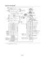
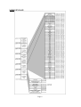
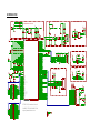
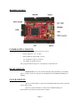
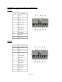
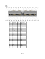
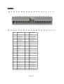
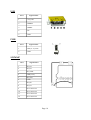
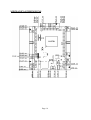
STM32-LCD development board
User's manual
All boards produced by Olimex are ROHS compliant
Revision C, May 2014
Copyright(c) 2014, OLIMEX Ltd, All rights reserved
Page 1
INTRODUCTION:
STM32-LCD is development prototype board with STM32F103ZE microcontroller from STMicroelectronics. This powerful microcontroller supports various
serial interfaces such as USB, USART, SPI. In addition you will find also accelerometer, JTAG, TFT LCD, mini SD/MMC card connector on this board and most
of the GPIOs are on extension headers where you can connect your additional circuits. All
this allows you to build a diversity of powerful applications to be used in a wide
range of situations.
BOARD FEATURES:
–
Microcontroller – STM32F103ZE – high-performance ARM® Cortex™-M3 32-bit
RISC core operating at a 72 MHz frequency, high-speed embedded memories
(Flash memory – 512 Kbytes and SRAM – 64 Kbytes), and an extensive range of
enhanced I/Os and peripherals connected to two APB buses.
–
JTAG connector
–
EXT connector
–
UEXT40 connector
–
UEXT1 connector
–
UEXT2 connector
–
EXT_PWR connector
–
Mini SD/MMC
–
Mini USB
–
LCD TFT 320x240 pixels colored with touch screen
–
Power source connector
–
Accelerometer
–
8 MHz crystal oscillator
–
Reset circuit
–
Clock circuit
–
PCB: FR-4, 1.5 mm (0,062"), soldermask, silkscreen component print
–
Dimensions 79.2x57.6 mm (3.12x2.27)”
Page 2
ELECTROSTATIC WARNING:
The STM32-LCD board is shipped in protective anti-static packaging. The board
must not be subject to high electrostatic potentials. General practice for working
with static sensitive devices should be applied when working with this board.
BOARD USE REQUIREMENTS:
Cables: The required cables depend on the programmer/debugger that you use.
Additionally, you might need USB mini cable for USB connection
Hardware: You need a JTAG or SWD debugger or programmer to be able to
program the board. The board has a standard 20-pin JTAG connector and typical
layout (further detailed later in the document).
You may check on our products ARM-JTAG-COOCOX, ARM-USB-OCD-H, ARMUSB-TINY-H.
PROCESSOR FEATURES:
–
–
–
–
STM32-LCD use High-density performance line ARM-based 32-bit MCU with
these features:
Core: ARM 32-bit Cortex™-M3 CPU
–
72 MHz maximum frequency, 1.25 DMIPS/MHz (Dhrystone 2.1) performance at 0 wait state memory access
–
Single-cycle multiplication and hardware division
Memories
–
512 Kbytes of Flash memory
–
64 Kbytes of SRAM
–
Flexible static memory controller with 4 Chip Select. Supports Compact
Flash, SRAM, PSRAM, NOR and NAND memories
–
LCD parallel interface, 8080/6800 modes
Clock, reset and supply management
–
2.0 to 3.6 V application supply and I/Os
–
POR, PDR, and programmable voltage detector (PVD)
–
4-to-16 MHz crystal oscillator
–
Internal 8 MHz factory-trimmed RC
–
Internal 40 kHz RC with calibration
–
32 kHz oscillator for RTC with calibration
Low power
Page 3
–
–
Sleep, Stop and Standby modes
–
VBAT supply for RTC and backup registers
3 × 12-bit, 1 µs A/D converters (up to 21 channels)
–
Conversion range: 0 to 3.6 V
–
Triple-sample and hold capability
–
Temperature sensor
–
2 × 12-bit D/A converters
–
DMA: 12-channel DMA controller
–
–
–
Debug mode
–
Serial wire debug (SWD) & JTAG interfaces
–
Cortex-M3 Embedded Trace Macrocell™
112 fast I/O ports
–
–
–
–
Supported peripherals: timers, ADCs, DAC, SDIO, I2Ss, SPIs, I2Cs and
USARTs
112 I/Os, all mappable on 16 external interrupt vectors, all 5 V-tolerant
except for analog inputs
11 timers
–
four 16-bit timers, each with up to 4 IC/OC/PWM or pulse counter and
quadrature (incremental) encoder input
–
2 × 16-bit motor control PWM timers with dead-time generation and
emergency stop
–
2 × watchdog timers (Independent and Window)
–
SysTick timer: a 24-bit downcounter
–
2 × 16-bit basic timers to drive the DAC
13 communication interfaces
–
2 × I2C interfaces (SMBus/PMBus)
–
5 USARTs (ISO 7816 interface, LIN, IrDA capability, modem control)
–
3 SPIs (18 Mbit/s), 2 with I2S interface multiplexed
–
CAN interface (2.0B Active)
–
USB 2.0 full speed interface
–
SDIO interface
CRC calculation unit, 96-bit unique ID
Page 4
BLOCK DIAGRAM:
Page 5
MEMORY MAP:
Page 6
SCHEMATIC:
BAT_PWR
VIN +5V_J-LINK
D4
1N5819S
D3
1N5819S
+5V_USB
D1
POWER SUPPLY CIRCUIT
1N5819S
PWR
D2
RF1
2
1N5819S
2
RF110_SMD
R17
4V_MIN-6V_MAX
1
VIN
#SHDN
330K/1%
3
C100
100nF
100uF/6.3V/tant
6
GND
GND
10K
Q3
BC807
3.3V
0R
R38
C33
C10
C99
1uF
100nF
MCP1825-ADJE/DC
R51
R4
1
1.5K
330R
10
3.3V
GND
R18
USBDP
22R
USBDM
VDD_1
10 8
VDD_2
14 4
VDD_3
39
VDD_4
17
VDD_5
52
VDD_6
62
VDD_7
84
VDD_8
95
VDD_9
12 1
VDD_10
13 1
VDD_11
PA03/WKUP/US
ART2_CTS/AD
C123 _IN0 /TIM5 _CH1/TIM2_CH1 _ETR/TIM8_ETR
4
USB_P
PA13/U
/A DC1 23_IN1/TIM5_CH2/TIM2 _CH2
5 SART2_RTSPA1
R21
22R
C16
72
0R
9
U9
0R
3.3V_MCU_E
R24
4.7K
4.7K
U5
ADJ5
47K/1%
3.3V
R23
100nF
20K
C96
3.3V
C58
3.3V
R10
R16
3.3V
USB_P
DISC
2K
R14
10K
C97
3.3V_E
VOUT
4
ACCELEROMETER
+5V_USB
R9
R36
47K/1%
VR1
1
USB CIRCUIT
3.3V
R22
1
2
4
3
C32
C17
47pF(NA)
6
5
V BUS
D-
C2
C4
2
10uF/10V
10uF/10V
3
D+
SCK6
SDO
7
NC1
NC2
I2C2_SCL
SDI/SDA
8
I2C2_SDA
VD DIO
VD D
INT4
3.3V
CSB5
GND
SENS_INT
SMB380,(QFN10)
ID
G ND
(NA)USBLC6-2P6
100nF
47pF(NA)
R41
1M
PA23/U
_CH3/ADC1 23_IN2/TIM2_CH3
6 SART2_TX/TIM5
USART2_TX
PA33/U
_CH4/ADC1 23_IN3/TIM2_CH4
7 SART2_RX/TIM5
USART2_RX
C80
10nF
PA44/S
C_O UT1 /U SART2_CK/ADC12_IN4
0 PI1_NSS /DASPI1_NSS
PA54/S
C_OUT2 /A DC12 _IN5
1 PI1_SCK/DASPI1_SCK
PA64/S
/TIM1 _B KIN
2 PI1_MIS O/TIM8_BKIN/ADC12_IN6/TIM3_CH1
SPI1_MISO
PA74/S
N/A DC1 2_IN7 /TIM3 _CH2/TIM1_CH1 N
3 PI1_MOSI/TIM8_CH1
SPI1_MOSI
PA81/U
SART1_CK/TIM1
00
PA8 _CH1/MCO
PA91/U
SART1_TX/TIM1
_CH2
01
USART1_TX
PA110/USA
RT1 _RX
/TIM 1_CH3
02
USART1_RX
PA111/USA
RT1 _CTS/CANRX/TIM1_CH4
/U SBDM
03
USBDM
PA112/USA
RT1 _RTS/CANTX/TIM1_ETR/USBD
P
04
USBDP
PA113/JTMS-SWDIO
05
TMS
PA114/JTCK-SWCLK
09
TCK
PA115/JTDI/S
PI3_NSS
10
TDI/I2S 3_WS /TIM2_CH1_ETR/S PI1_NSS
B1_0/B1_1
VBAT
71
VSS _1
10 7
VSS _2
14 3
VSS _3
38
VSS _4
16
VSS _5
51
VSS _6
61
VSS _7
83
VSS _8
94
VSS _9
12 0
VSS _10
13 0
VSS _11
3.3V
B0_1/B0_0
1
3
3.3V_A
33
3.3V_A
0
C11
VREF+
47R R20
C9
R40
10uF/6.3V
100nF
0R
100nF
C47
32
NA
C79
31
30
6
R15
C12
27pF
23
R12
Q1
8MHz
U2
NA
VCC
NA
R69
1
C28
100nF
EXT
3.3V
1
2
3
4
PE1
PE6
PC7
PB5
5
6
7
8
9
10
+5V_USB 11
13
PG15
15
PG13
17
PG11
19
PG9
21
PG7
23
PG5
25
PG3
27
PG1
12
29
30
VBAT
PD12
PB2
PA1
VIN
PF0
PF1
PF2
PF3
PF4
PF5
PF6
PF7
PF8
PF9
PF10
PF11
PF12
PF13
PF14
PF15
14
PG14
PG12
PG10
PG8
PG6
PG4
PG2
PG0
16
18
20
22
24
26
28
31
32
33
34
35
36
37
38
39
RST
PD6
PD11
USB_P
PA8
40
25
PG0
PG1
PG2
PG3
PG4
PG5
PG6
PG7
PG8
PG9
PG10
PG11
PG12
PG13
PG14
PG15
RST
560R
GND
3.3V
PE0
PE5
PC6
PC13
VREFVSS A
VBAT
BH40R
OSC_IN
OSC_OUT
10 6
NC
RST
10K
RE SET
24
R19
390R
C13
27pF
R8
2
VREF+
13 8
BOOT0
10K
3.3V
VDDA
56
57
87
88
89
90
91
92
93
NRST
PG0/FSMC_A10
PG1/FSMC_A11
PG2/FSMC_A12
PG3/FSMC_A13
PG4/FSMC_A14
PG5/FSMC_A15
PG6/FSMC_INT2
PG7/FSMC_INT3
PG8
12 4
PG9/FSMC_NE2 /FSMC_NCE 3
12 5
PG10 /FSMC_NCE4_1/FS MC_NE3
12 6
PG11 /FSMC_NCE4_2
12 7
PG12 /FSMC_NE 4
12 8
PG13 /FSMC_A2 4
12 9
PG14 /FSMC_A2 5
13 2
PG15
10
11
12
13
14
15
18
19
20
21
22
49
50
53
54
55
PF0 /FSMC_A0
PF1 /FSMC_A1
PF2 /FSMC_A2
PF3 /FSMC_A3
PF4 /FSMC_A4
PF5 /FSMC_A5
PF6 /A DC3_IN4/FS MC_NIO RD
PF7 /A DC3_IN5/FS MC_NREG
PF8 /A DC3_IN6/FS MC_NIO WR
PF9 /A DC3_IN7/FS MC_CD
PF1 0/ADC3 _IN8 /FSMC_INTR
PF1 1/FSM C_NIOS 16
PF1 2/FSM C_A 6
PF1 3/FSM C_A 7
PF1 4/FSM C_A 8
PF1 5/FSM C_A 9
PB04/A
_CH3/TIM8_CH2 N/TIM1_CH2N
6 DC1 2_IN8 /TIM3
ADC12_IN8
PB14/A
_CH4/TIM8_CH3 N/TIM1_CH3N
7 DC1 2_IN9 /TIM3
ADC12_IN9
3
1
PB41/JNTRST/S
PI3_MIS
34
TRSTO/TIM3_CH1 /S PI1_M IS O
PB51/I2C1_SMBA
I/SPI3
35
PB5 _MOS I/I2S 3_S D/TIM3_CH2/SPI1_MO SI
PB81/TIM4_CH3/SDIO_D4/I2C1
39
I2C1_SCL2 _S CL/CANRX
PB91/TIM4_CH4/SDIO_D5/I2C1
40
I2C1_SDA2 _S DA/CANTX
PB160/I2
9 C2_SCL/USART3_TX
I2C2_SCL /TIM2 _CH3
I2C1_SCL1
5
SPI1_MISO
SPI1_SCK7
3.3V
3.3V_A
DACOUT1
DACOUT2
9
2
I2C1_SDA1
SPI1_MOSI
SPI1_NSS
6
8
10
+5V_USB11
13
PF15
15
PF13
17
PF11
19
PF9
21
PF7
23
PF5
25
PF3
27
PF1
12
29
30
31
32
VREF+ 33
35
SPI1_NSS
37
SPI1_SCK
34
39
USART1_RX
4
14
16
18
20
22
24
26
28
PF14
PF12
PF10
PF8
PF6
PF4
PF2
PF0
36
38
40
BH40R
RST
ADC12_IN8
ADC12_IN9
ADC12_IN14
ADC12_IN15
VIN
R150
R155
10K
10K
NA
JTAG
10K
R151
10K
R153
R154
10K
10K
1
2
+5V_J-LINK
R-T
UEXT2_3.3V
3.3V
1
2
3
4
5
6
7
8
3.3V
0R
3.3V
100nF
C19
9
10
R118
11
12
13
14
4.7K
15
16
17
18
19
20
UEXT2
USART2_TX
I2C1_SCL2
SPI2_MISO
SPI2_SCK
BH20R
PB175/SPI2
_MOS I/I2S2
_S D/TIM 1_CH3N
6
SPI2_MOSI
1
2
3
4
5
6
7
8
9
10
R119
R120
4.7K
33K
USART2_RX
I2C1_SDA2
SPI2_MOSI
SPI2_NSS
BH10R
PC02/A
6 DC1 23_IN10
YD
PC12/A
7 DC1 23_IN11
YU
PC22/A
8 DC1 23_IN12
XL
PC32/A
9 DC1 23_IN13
XR
PC44/A
4 DC1 2_IN1 4ADC12_IN14
PC54/A
5 DC1 2_IN1 5ADC12_IN15
PC69/I2S
6 2_MCK/TIM8
PC6_CH1/SDIO_D 6/TIM3_CH1
UEXT1
PC79/I2S
7 3_MCK/TIM8
PC7_CH2/SDIO_D 7/TIM3_CH2
PC89/TIM8_CH3/SDIO_D0/TIM3
_CH3
SD_D0
8
SD/MMC CARD
PC99/TIM8_CH4/SDIO_D1/TIM3
_CH4
SD_D1
9
PC110/UART4_TX/SD
IO _D2 /US ART3_TX
SD_D2
11
PC111/UART4_RX/SD
IO_D3/US ART3_RX
SD_D3
12
PC112/UART5_TX/SD
IO _CK/U SART3_CK
SD_CLK
13
PC173/TAM PER-RTC
PC13
PC184/OSC32_IN
NA
PC195/OSC32_OUT
R104
UEXT1_3.3V
3.3V
C15
Q2
32768/6pF
C14
GND
3.3V
R6
UEXT1
4.7K
10pF
R108
33K
R107
33K
USART1_TX
I2C1_SCL1
SPI1_MISO
SPI1_SCK
USD
PD31/FSMC_CLK/USA
RT2 _CTS
17
DISC
PD41/FSMC_NOE
/U
SART2_RTS
18
/OE
10
12
PD51/FSMC_NWE
/US
ART2_TX
19
/WE
PD61/FSMC_NWAIT/US
22
PD6 ART2_RX
PD71/FSMC_NE
1/FSMC_NCE2/US
ART2_CK
23
/NCE2
SD_D3
SD_CMD
PD87/FSMC_D13
/UD13
SART3_TX
7
PD97/FSMC_D14
/UD14
SART3_RX
8
SD_D3
SD_CMD
2
3
6
3.3V
PD170/FSM
C_D1 5/USA
9
D15 RT3 _CK
PD181/FSM
C_A 16/USA
0
PD11RT3 _CTS
SD_CLK
SD_D0
SD_D1
SD_D2
PD182/FSM
C_A 17/TIM4_CH1
/U SART3_RTS
1
PD12
PD183/FSM
C_A 18/TIM4_CH2
2
TFT_LIGHT
3.3V
3.3V
3.3V
PD184/FSM
C_D0 /TIM4_CH3
D0
5
PD185/FSM
C_D1 /TIM4_CH4
D1
6
PE01/TIM4_E
TR/FSMC_NBL0
41
PE0
PE11/FSMC_NB
L1 PE1
42
L5
470nH
4
SD_CLK
SD_D0
SD_D1
SD_D2
5
7
8
1
R106 33K
R100 33K
R105 33K
9
11
C20
PE21/TRACECK/FSMC_A2
3
TFT_RST
PE32/TRACED0 /FSMC_A19
TFT_RS
47uF/6.3V
PE43/TRACED1 /FSMC_A20
SENS_INT
PE54/TRACED2 /FSMC_A21
PE5
PE65/TRACED3 /FSMC_A22
PE6
PE75/FSMC_D4
/TIM1
D4_E TR
8
PE85/FSMC_D5
/TIM1
D5_CH1N
9
WP1
PE161/FS
4 MC_D 8/TIM1_CH2
D8
PE162/FS
5 MC_D 9/TIM1_CH3N
D9
PE163/FS
6 MC_D 10/TIM1_CH3
D10
PE164/FS
7 MC_D 11/TIM1_CH4
D11
PE165/FS
8 MC_D 12/TIM1_BKIN
D12
1
2
3
4
5
6
7
8
9
10
WP2
CON6
1
+5V_USB
2
3
4
5
6
EXT_PWR
BAT_PWR
R13
4.7K
33K
BH10R
CMD/DI
V SS
V DD
CLK/SCLK
3.3V
3.3V
3.3V
D AT0 /DO
D AT1 /RES
D AT2 /RES
R2
R7
R3
NA
NA
NA
3.3V
CP1
CP2
MICRO_SD_CARD_holder
TFT_RST
/NCE2
TFT_RS
/WE
/OE
TFT
#RESE T
8
#CS
4
5
RS
6
#WR
7
#RD
9
DB 0
1 0 DB 1
1 1 DB 2
1 2 DB 3
1 3 DB 4
1 4 DB 5
1 5 DB 6
1 6 DB 7
1 7 DB 8
1 8 DB 9
1 9 DB 10
2 0 DB 11
2 1 DB 12
2 2 DB 13
2 3 DB 14
2 4 DB 15
2
VCC
3
VCC
C1
C3
100nF
100nF
1
GND
25
GND
YD
XL
YU
XR
26
27
28
29
35
LE DA
36
LE DA
YD
XL
YU
XR
3.3V
R_LCD
30
LE DK1
31
LE DK2
32
LE DK3
33
LE DK4
34
LE DK5
37
GND
FS-K320QVB-V1
OLIMEX LTD, BULGARIA 2014
R11
USART1_RX
I2C1_SDA1
SPI1_MOSI
SPI1_NSS
CD/DAT3 /CS
D0
D1
D2
D3
D4
D5
D6
D7
D8
D9
D10
D11
D12
D13
D14
D15
PE96/FSMC_D6
/TIM1
D6_CH1
0
PE160/FS
3 MC_D 7/TIM1_CH2N
D7
3.3V
100nF
C18
10pF
PD01/O
NRX
D2
14SC_IN/FSMC_D2/CA
PD11/O
D3
15SC_OUT/FSMC_D3/CANTX
PD21/TIM
RT5 _RX /S DIO _CM D
16 3_E TR/UA
SD_CMD
3.3V
0R
3.3V
STM32-LCD, board revision A
https://www.olimex.com
R147
10K
R149
TRST
PB173/SPI2
_SCK/I2
S2_CK/US ART3_CTS/TIM1 _CH1N
4
SPI2_SCK
PB174/SPI2
_MISO/US
ART3_RTS/TIM1 _CH2N
5
SPI2_MISO
UEXT40
3
R148
10K
TDO
RST
PB171/I2
SART3_RX/TIM2_CH4
0 C2_SDA /U
I2C2_SDA
PB172/SPI2
_NS S/I2
S2_WS/I2 C2_SMB AI/U SART3_CK/TIM1_BKIN
3
SPI2_NSS
3.3V
1
USART1_TX
R152
TRST
TDI
TMS
TCK
PB61/I2C1_SCL/TIM4
_CH1/USA RT1 _TX
36
I2C1_SCL1
PB71/I2C1_SDA/FS
MC_NL/TIM4 _CH2/USART1_RX
37
I2C1_SDA1
UEXT2
3.3V
3.3V
R54
PB24/B
PB2
8 OOT1
10K
PB31/TRACESWO
/JTDO
33
TDO /S PI3_SCK/I2S 3_CK/TIM2_CH2 /S PI1_S CK
0R
FET1
IRLML6402
R1
100K
R50
1.5K
TFT_LIGHT
BOARD LAYOUT
POWER SUPPLY CIRCUIT:
STM32-LCD can take power from four sources:
–
Power connector – 4V – 6V DC.
–
BAT_PWR from EXT_PWR – 4V DC.
–
+5V_J-LINK from JTAG connector
–
+5V_USB from USB connector
The programmed board power consumption is about 200 mA.
RESET CIRCUIT:
STM32-LCD reset circuit includes R8 (10k), R69 (560 Ohm), C28 (100nF)
pin 15 of JTAG connector, EXT pin 32, UEXT40 pin 32 and STM32F103ZE pin 25
(NRST).
CLOCK CIRCUIT:
Quartz crystal 8 MHz is connected to STM32F103ZE pin 23 (OSC_IN) and
pin 24 (OSC_OUT).
Quartz crystal 32.768 kHz is connected to STM32F103ZE pin 8
(PC14/OSC32_IN) and pin 9 (PC15/OSC32_OUT).
Page 8
JUMPER DESCRIPTION:
R-T
Connect RST with TRST.
Default state is open.
UEXT1_3.3V
This jumper when closed, supplies 3.3 V voltage to UEXT1 pin 1.
Default state is closed.
UEXT2_3.3V
This jumper when closed, supplies 3.3 V voltage to UEXT2 pin 1.
Default state is closed.
3.3V_E
This jumper, when closed, enable the main 3.3 V regulator VR1 - MCP1825-ADJE/DC.
Default state is closed.
3.3V_MCU_E
This jumper, when closed, enables STM32F103ZE 3.3 V power supply.
Default state is closed.
R_LCD
You can use this jumper, when it's open, to measure the current of LCD backlight.
Default state is closed.
B0_1/B0_0
Select BOOT0 Boot mode.
Default state is in position B0_0.
B1_0/B1_1
Select BOOT1 Boot mode.
Default state – B1_0 – not shorted and B1_1 – not shorted.
Boot mode selection pins Boot Mode
Aliasing
BOOT1
BOOT0
x
0
Main Flash memory Main Flash memory is selected as boot space
0
1
System memory
System memory is selected as boot space
1
1
Embedded SRAM
Embedded SRAM is selected as boot space
INPUT/OUTPUT:
–
LCD TFT 320x240 pixels colored with touch screen.
Page 9
EXTERNAL CONNECTORS DESCRIPTION:
UEXT1
Pin #
Signal Name
1
3.3V
2
GND
3
USART1_TX
4
USART1_RX
5
I2C1_SCL1
6
I2C1_SDA1
7
SPI1_MISO
8
SPI1_MOSI
9
SPI1_SCK
10
SPI1_NSS
UEXT2
Pin #
Signal Name
1
3.3V
2
GND
3
USART2_TX
4
USART2_RX
5
I2C1_SCL2
6
I2C1_SDA2
7
SPI2_MISO
8
SPI2_MOSI
9
SPI2_SCK
10
SPI2_NSS
Page 10
EXT
Pin #
Signal Name
Pin #
Signal Name
1
3.3 V
2
GND
3
PE0
4
PE1
5
PE5
6
PE6
7
PC6
8
PC7
9
PC13
10
PB5
11
3.3 V
12
GND
13
+5V_USB
14
VIN
15
PG15
16
PG14
17
PG13
18
PG12
19
PG11
20
PG10
21
PG9
22
PG8
23
PG7
24
PG6
25
PG5
26
PG4
27
PG3
28
PG2
29
PG1
30
PG0
31
VBAT
32
RST
33
GND
34
PD6
35
PD12
36
PD11
37
PB2
38
USB_P
39
PA1
40
PA8
Page 11
UEXT40
Pin #
Signal Name
Pin #
Signal Name
1
3.3 V
2
GND
3
USART1_TX
4
USART1_RX
5
I2C1_SCL1
6
I2C1_SDA1
7
SPI1_MISO
8
SPI1_MOSI
9
SPI1_SCK
10
SPI1_NSS
11
3.3 V
12
GND
13
+5V_USB
14
VIN
15
PF15
16
PF14
17
PF13
18
PF12
19
PF11
20
PF10
21
PF9
22
PF8
23
PF7
24
PF6
25
PF5
26
PF4
27
PF3
28
PF2
29
PF1
30
PF0
31
3.3V_A
32
RST
33
AGND
34
ADC12_IN8
35
VREF+
36
ADC12_IN9
37
SPI1_NSS
38
ADC12_IN14
39
SPI1_SCK
40
ADC12_IN15
Page 12
JTAG:
The JTAG connector allows a debugger or programmer to talk via a JTAG (Joint Test Action Group)
port directly to the core. Instructions may be inserted and executed by the core thus allowing
STM32F103ZE memory to be programmed with code and executed step by step by the host software.
Pin #
Signal Name
Pin #
Signal Name
1
3.3V
2
3.3V
3
TRST
4
GND
5
TDI
6
GND
7
TMS
8
GND
9
TCK
10
GND
11
pull-down
12
GND
13
TDO
14
GND
15
RST
16
GND
17
pull-down
18
GND
19
+5V J-LINK
20
GND
Page 13
USB
Pin #
Signal Name
1
+5V_USB
2
USBDM
3
USBDP
4
NC
5
GND
PWR
Pin #
Signal Name
1
VIN (4 – 6) V DC
2
GND
SD/MMC
Pin #
Signal Name
1
SD_D2
2
SD_D3
3
SD_CMD
4
VDD (3.3V)
5
SD_CLK
6
GND
7
SD_D0
8
SD_D1
9
Not connected
10
Not connected
11
Not connected
12
Not connected
Page 14
SPI
Up to three SPIs are able to communicate up to 18 Mbits/s in slave and
master modes in full-duplex and simplex communication modes. The 3-bit prescaler
gives 8 master mode frequencies and the frame is configurable to 8 bits or 16 bits.
The hardware CRC generation/verification supports basic SD Card/MMC modes.
All SPIs can be served by the DMA controller.
I2S
Two standard I2S interfaces (multiplexed with SPI2 and SPI3) are available,
that can be operated in master or slave mode. These interfaces can be configured to
operate with 16/32 bit resolution, as input or output channels. Audio sampling
frequencies from 8 kHz up to 48 kHz are supported. When either or both of the I2S
interfaces is/are configured in master mode, the master clock can be output to the
external DAC/CODEC at 256 times the sampling frequency.
I2C
Up to two I²C bus interfaces can operate in multimaster and slave modes.
They can support standard and fast modes.
They support 7/10-bit addressing mode and 7-bit dual addressing mode (as
slave). A hardware CRC generation/verification is embedded.
They can be served by DMA and they support SMBus 2.0/PMBus.
Page 15
MECHANICAL DIMENSIONS
Page 16
AVAILABLE DEMO SOFTWARE
–
EW-ARM general demo code – the code of the initial STM32-LCD demo
–
EW-ARM Demo code for MOD-GSM and MOD-GSM-EDGE - (high speed) GSM
modules connected to STM32-LCD
Page 17
ORDER CODE: STM32-LCD – assembled and tested board
How to order?
You can order directly from us or from any of our distributors.
Please check our web-site https://www.olimex.com for more info.
Revision history:
Manual revision:
Rev. Initial, May 2009
Rev. A, June 2011 – changed schematic
Rev. B, October 2011 – added more detailed
mechanical dimensions
Rev. C, May 2014 – updated board schematic,
added board revision history, updated disclaimer,
updated links
Board revision:
Rev. Initial, May 2009
Rev. A, May 2014
1. The analog GND got properly connected to the
digital GND through a 0 Ohm resistor
2. Fixed the JTAG label (was “JATG” before)
3. The LCD GND got properly connected
4. The cathodes of the LCD 's backlight got
connected to GND
5. C1 i C3 are moved further away from the LCD
connector
6. The accelerometer is changed from LISxx to
SMB380
7. Added RC filter to the power suppl of SMB380
Page 18
Disclaimer:
© 2014 Olimex Ltd. Olimex®, logo and combinations thereof, are registered trademarks of Olimex Ltd. Other
product names may be trademarks of others and the rights belong to their respective owners.
The information in this document is provided in connection with Olimex products. No license, express or
implied or otherwise, to any intellectual property right is granted by this document or in connection with
the sale of Olimex products.
It is possible that the pictures in this manual differ from the latest revision of the board.
The product described in this document is subject to continuous development and improvements. All particulars
of the product and its use contained in this document are given by OLIMEX in good faith. However all
warranties implied or expressed including but not limited to implied warranties of merchantability or fitness for
purpose are excluded. This document is intended only to assist the reader in the use of the product. OLIMEX
Ltd. shall not be liable for any loss or damage arising from the use of any information in this document or any
error or omission in such information or any incorrect use of the product.
This evaluation board/kit is intended for use for engineering development, demonstration, or evaluation purposes
only and is not considered by OLIMEX to be a finished end-product fit for general consumer use. Persons
handling the product must have electronics training and observe good engineering practice standards. As such,
the goods being provided are not intended to be complete in terms of required design-, marketing-, and/or
manufacturing-related protective considerations, including product safety and environmental measures typically
found in end products that incorporate such semiconductor components or circuit boards.
Olimex currently deals with a variety of customers for products, and therefore our arrangement with the user is
not exclusive. Olimex assumes no liability for applications assistance, customer product design, software
performance, or infringement of patents or services described herein.
THERE IS NO WARRANTY FOR THE DESIGN MATERIALS AND THE
COMPONENTS USED TO CREATE STM32-LCD. THEY ARE CONSIDERED
SUITABLE ONLY FOR STM32-LCD.
Page 19