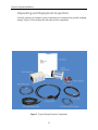
1
SYNAPSE
CCD Detection System
User Manual
Part Number 81100 – Revision 2
Copyright © November, 2006 HORIBA Jobin Yvon Inc., Optical Spectroscopy Division.
All rights reserved. Portions of the software described in this document Copyright ©
Microsoft Corporation. All rights reserved.
No part of this document may be reproduced, stored in a retrieval system, or transmitted
in any form by any means, including electronic or mechanical, photocopying and
recording without prior written permission of HORIBA Jobin Yvon Inc., Optical
Spectroscopy Division. Requests for permission should be submitted in writing.
Information in this document is subject to change without notice and does not represent a
commitment on the part of the vendor.
ii
Contents
DISCLAIMER............................................................................................................................VII
PREFACE.................................................................................................................................... IX
CHAPTER 1: SYSTEM DESCRIPTION AND SPECIFICATIONS.......................................1
Introduction ................................................................................................................................. 1
CHAPTER 2: SYSTEM REQUIREMENTS ..............................................................................5
Input Power Requirements .......................................................................................................... 5
Environmental Requirements ...................................................................................................... 5
Ventilation Requirements ............................................................................................................ 5
General Safety Requirements ...................................................................................................... 6
Safety Symbols ............................................................................................................................ 7
Computer Requirements .............................................................................................................. 9
Software ................................................................................................................................... 9
Hardware .................................................................................................................................. 9
General Maintenance Requirements.......................................................................................... 10
Cleaning the Detector Head ................................................................................................... 10
Cleaning the Dust Cover of the Power Supply Unit .............................................................. 10
CHAPTER 3: DETECTOR SYSTEM INSTALLATION .......................................................11
Installation Overview ................................................................................................................ 11
Unpacking and Equipment Inspection....................................................................................... 12
Installing SynerJY Application Software .................................................................................. 14
Mounting Synapse to a Spectrograph........................................................................................ 15
Connecting Electrical Interface Cables ..................................................................................... 16
CHAPTER 4: INITIAL POWER-UP AND OPERATION .....................................................19
Initial Power-up ......................................................................................................................... 19
CCD Focus and Alignment on the Spectrograph ...................................................................... 22
Preparing Focus and Alignment Mechanisms........................................................................ 22
Synapse Focus and Alignment ............................................................................................... 23
Modes of Data Acquisition........................................................................................................ 25
CCD Position.......................................................................................................................... 25
CCD Range ............................................................................................................................ 26
Triggering............................................................................................................................... 26
Acquisition Mode Parameters ................................................................................................ 26
CHAPTER 5: TRIGGERING ....................................................................................................29
TTL Output Options: ................................................................................................................. 29
SHUTTER.............................................................................................................................. 29
START EXPERIMENT......................................................................................................... 29
EXT TRIGGER READY ....................................................................................................... 29
Synchronized Triggering to an External Event ......................................................................... 30
iii
Contents
CHAPTER 6: AUXILIARY ANALOG INPUT........................................................................33
Normalization (Reference) ........................................................................................................ 33
Independent Data Acquisition ................................................................................................... 35
Configuring for Voltage and Current Modes ............................................................................ 36
CHAPTER 7: TEMPERATURE CONTROL ..........................................................................37
CHAPTER 8: DETECTOR SYSTEM COMPONENT DESCRIPTION ..............................39
Synapse CCD Detector Head .................................................................................................... 39
Detector Head Cooling........................................................................................................... 39
Detector Head Chamber and Cooling Effectiveness.............................................................. 40
Detector Head Electrical Interfaces........................................................................................ 40
SHUTTER.............................................................................................................................. 41
START EXPERIMENT......................................................................................................... 41
EXT TRIGGER READY ....................................................................................................... 42
Pixel Processing / Data Acquisition Modes of Operation...................................................... 44
Gain Selections....................................................................................................................... 45
System Noise.......................................................................................................................... 47
Built-In-Test Diagnostic Capability ....................................................................................... 49
CCD Hardware Binning Control............................................................................................ 49
CCD Exposure Control .......................................................................................................... 49
Synapse Power Supply Unit ...................................................................................................... 51
Integrated TE Power Supply .................................................................................................. 51
Integrated Power Shutter Drive Circuitry (optional).............................................................. 51
Power Supply Unit Electrical Interfaces ................................................................................ 52
Software..................................................................................................................................... 53
Shutter........................................................................................................................................ 53
CHAPTER 9: POWERING DOWN AND DISASSEMBLY OF THE SYSTEM .................55
Power Down Procedure ............................................................................................................. 55
Disassembly of the Detection System ....................................................................................... 55
CHAPTER 10: OPTIMIZATION AND TROUBLESHOOTING..........................................57
Optical Optimization ................................................................................................................. 57
Spatial Optimization .................................................................................................................. 57
Reducing the Number of Conversions....................................................................................... 58
Environmental Noise Reduction................................................................................................ 58
Cooling ...................................................................................................................................... 59
Shutter........................................................................................................................................ 59
Power Interruption..................................................................................................................... 59
Software Cannot Recognize Hardware Configuration ............................................................ 59
Unit Fails to Turn On................................................................................................................. 60
APPENDIX A: DIMENSIONAL DRAWINGS ........................................................................61
APPENDIX B:
COMPLIANCE INFORMATION..........................................................65
Declaration of Conformity......................................................................................................... 65
Supplementary Information.................................................................................................... 65
iv
Contents
APPENDIX C: PERFORMING ROUTINE PROCEDURES WITH SYNERJY.................67
CCD Focus and Alignment on the Spectrograph ...................................................................... 67
Triggering .................................................................................................................................. 71
Using the Auxiliary Analog Input Port...................................................................................... 73
Normalization (Reference)..................................................................................................... 73
Independent Data Acquisition................................................................................................ 74
Configuring for Voltage and Current Modes ......................................................................... 75
APPENDIX D: WEEE RECYCLING PASSPORT .................................................................77
WEEE Product Marking............................................................................................................ 79
General External View of Detector Head.................................................................................. 81
Dismantling of Detector Head................................................................................................... 82
Notes for Dismantling Detector Head ....................................................................................... 83
Complete Recycling Data of Detector Head ............................................................................. 84
General External View of Power Supply Unit .......................................................................... 85
Dismantling of Power Supply Unit ........................................................................................... 86
Notes for Dismantling Power Supply Unit................................................................................ 87
Complete Recycling Data of Power Supply Unit...................................................................... 88
APPENDIX E: ACCESSORIES.................................................................................................89
SERVICE POLICY .....................................................................................................................91
RETURN AUTHORIZATION...................................................................................................92
WARRANTY................................................................................................................................93
INDEX.........................................................................................................................................105
v
Contents
FIGURES
Figure 1. Removable Dust Cover of Power Supply Unit.............................................................. 10
Figure 2. Typical Synapse System Components........................................................................... 12
Figure 3. Flange Installation (Imaging flange pictured with iHR320 Spectrograph) ................... 15
Figure 4. Typical Synapse Electrical Interconnect Scheme.......................................................... 17
Figure 5. CCD Rotation and Adjustment Mechanisms ................................................................ 23
Figure 6. Example of a Focused and Aligned CCD...................................................................... 24
Figure 7. Timing Diagram for an Externally Triggered Single .................................................... 31
Figure 8. Timing Diagram for an Externally Triggered Multi-accumulation............................... 32
Figure 9. Typical Configuration for Normalization using Synapse AUX IN Port ....................... 33
Figure 10. Typical Configuration for Independent Data Acq. using Synapse AUX IN Port ....... 35
Figure 11. Detector Head Electrical Interfaces............................................................................. 40
Figure 12. External I2C Connector Pin Out (viewed looking at rear of detector) ........................ 43
Figure 13. Typical Dark/Noise Scan for the Synapse in High Sensitivity Mode ......................... 48
Figure 14. Illustration of 2 x 2 Binning Operation on a 4 x 4 CCD Array ................................... 50
Figure 15. Power Supply Unit Electrical Interfaces ..................................................................... 52
Figure 16. Synapse Detector Head................................................................................................ 61
Figure 17. Distance from Focal Plane to CCD Chip .................................................................... 62
Figure 18. Synapse Power Supply Unit ........................................................................................ 63
Figure 19. Synapse Detector Head Product Markings.................................................................. 80
Figure 20. Synapse Power Supply Unit Product Markings .......................................................... 80
Figure 21. General View of Synapse Detector Head Indicating Ext. Material for Recycling...... 81
Figure 22. Illustration of the Dismantling Process for the Synapse Detector Head ..................... 82
Figure 23. Synapse Detector Head Depicting Location of Internal Material for Recycling ........ 83
Figure 24. General View of Synapse Power Supply Unit Indicating Ext. Material for Recycling 85
Figure 25. Illustration of the Dismantling Process for the Synapse Power Supply Unit.............. 86
Figure 26. Synapse Power Supply Unit Depicting Location of Internal Material for Recycling. 87
TABLES
Table I. System Level Specifications for the Synapse CCD Detection System ............................. 2
Table II. Safety Symbols................................................................................................................. 7
Table III. Individual Components for the Synapse....................................................................... 13
Table IV. Synapse Gain Options Versus Sensor Offerings .......................................................... 45
Table V. Shutter Models ............................................................................................................... 54
Table VI. Applicable CE Compliance Tests and Standards ......................................................... 66
Table VII. Summary of Synapse Detection System Material Requiring Selective Treatment..... 77
Table VIII. Tools Required for Disassembly of the Synapse CCD Detection System................. 78
Table IX. Breakdown of Synapse Recycling Components Viewed Externally............................ 81
Table X. Detector Head Disassembly Process.............................................................................. 82
Table XI. Breakdown of Internal Detector Head Recycling......................................................... 83
Table XII. Complete Recycling Data of Detector Head ............................................................... 84
Table XIII. Breakdown of Power Supply Unit Recycling Components Viewed Externally........ 85
Table XIV. Power Supply Unit Disassembly Process .................................................................. 86
Table XV. Breakdown of Internal Power Supply Unit Recycling................................................ 87
Table XVI. Complete Recycling Data of Power Supply Unit ...................................................... 88
Table XVII. Available Accessories for Synapse .......................................................................... 89
vi
Disclaimer
By setting-up or starting to use any HORIBA Jobin Yvon product, you are accepting the
following terms:
You are responsible for understanding the information contained in this document. You
should not rely on this information as absolute or all-encompassing; there may be local
issues (in your environment) not addressed in this document that you may need to
address, and there may be issues or procedures discussed that may not apply to your
situation.
If you do not follow the instructions or procedures contained in this document, you are
responsible for yourself and your actions and all resulting consequences. If you rely on
the information contained in this document, you are responsible for:
•
Adhering to safety procedures
•
Following all precautions
•
Referring to additional safety documentation, such as Material Safety Data Sheets
(MSDS), when advised
As a condition of purchase, you agree to use safe operating procedures in the use of all
products supplied by HORIBA Jobin Yvon, including those specified in the MSDS
provided with any chemicals and all warning and cautionary notices, and to use all safety
devices and guards when operating equipment. You agree to indemnify and hold
HORIBA Jobin Yvon harmless from any liability or obligation arising from your use or
misuse of any such products, including, without limitation, to persons injured directly or
indirectly in connection with your use or operation of the products. The foregoing
indemnification shall in no event be deemed to have expanded HORIBA Jobin Yvon’s
liability for the products.
HORIBA Jobin Yvon products are not intended for any general cosmetic, drug, food, or
household application, but may be used for analytical measurements or research in these
fields, or for forensic applications. A condition of HORIBA Jobin Yvon’s acceptance of a
purchase order is that only qualified individuals, trained and familiar with procedures
suitable for the products ordered, will handle them. Training and maintenance procedures
may be purchased from HORIBA Jobin Yvon at an additional cost. HORIBA Jobin Yvon
cannot be held responsible for actions your employer or contractor may take without
proper training.
Due to HORIBA Jobin Yvon’s efforts to continuously improve our products, all
specifications, dimensions, internal workings, and operating procedures are subject to
change without notice. All specifications and measurements are approximate, based on a
standard configuration; results may vary with the application and environment. Any
software manufactured by HORIBA Jobin Yvon is also under constant development and
subject to change without notice.
Any warranties and remedies with respect to our products are limited to those provided in
writing as to a particular product. In no event shall HORIBA Jobin Yvon be held liable
vii
Disclaimer
for any special, incidental, indirect or consequential damages of any kind, or any
damages whatsoever resulting from loss of use, loss of data, or loss of profits, arising out
of or in connection with our products or the use or possession thereof. HORIBA Jobin
Yvon is also in no event liable for damages on any theory of liability arising out of, or in
connection with, the use or performance of our hardware or software, regardless of
whether you have been advised of the possibility of damage.
viii
Preface
This manual explains how to install, operate, troubleshoot and maintain your Synapse
CCD (Charge Coupled Device) detection system, as well as describes salient features and
overall system specifications. Information is also provided regarding the minimum
system requirements necessary for successful system operation and optimum
performance.
Depending on the purchased system configuration, your system may contain more than
one HORIBA Jobin Yvon operating manual. The general guidelines presented below may
assist you in finding the specific manual that is the most informative on a particular
subject:
•
Each manual generally covers a specific product along with the features and
accessories particular to and/or contained within that product.
•
Accessories that can be applied to other products are normally covered by
separate documentation.
•
Software that is exclusively used with one instrument or system is covered in the
manual for that product.
•
Software that can be used with a number of products is covered in its own
manual.
•
If you are reading about a product that interacts with other products, you will be
referred to additional documentation as necessary.
ix
Preface
x
Chapter 1: System Description and
Specifications
Introduction
The Synapse CCD is a complete solution for modern
spectroscopic measurements. This compact CCD
detector is designed to interact with all HORIBA
Jobin Yvon spectrometers and provide highly
sensitive detection for any experiment. Its flexible
design can handle any application from simple
absorbance to the most difficult Raman or
photoluminescence measurements.
Synapse is a complete CCD detection system, providing two-dimensional photodetection, while offering outstanding sensitivity, high speed, low noise, ruggedness,
durability, and high reliability. The Synapse platform supports a wide variety of chip
formats and sensor characteristics to meet your intended spectroscopic application. Every
Synapse CCD is factory tested for linearity, full well capacity, and read noise
performance.
Features include an integrated controller, thermoelectric air cooling, and a maintenancefree, sealed vacuum chamber. Low noise amplifiers are precisely located next to the CCD
sensor to minimize any noise from the external environment. Communication between
the detector and the host computer is achieved via a high speed USB 2.0 computer
interface.
Additionally, Synapse allows flexibility in selection and storage of detector parameters
for X and Y binning, area definition, selection of various gains and pixel processing
speeds, and advanced trigger operation as well as TTL output. All functions are
controlled via SynerJY®, HORIBA Jobin Yvon’s spectroscopic application software.
The primary components making up the Synapse CCD detection system are:
•
CCD Detector Head
•
Power Supply Unit
•
Spectroscopic Application Software
All Synapse equipment is tested for compliance with both the EMC Directive
89/336/EEC and the Low Voltage Directive for Safety 73/23/EEC, and bears the
international CE mark as indication of this compliance. HORIBA Jobin Yvon guarantees
the product line’s CE compliance only when original HORIBA Jobin Yvon supplied parts
are used. Appendix B provides a table of all CE Compliance tests and standards used to
qualify this product.
1
System Description and Specifications
Table I. System Level Specifications for the Synapse CCD Detection System
Specifications
System Parameter
Units / Description
Sensor
Temperature
-70 °C (203 K) @ TA = +20 °C
Operating
Resolution Step Size
0.1 °C
Temperature
Long Term Stability
± 0.1 °C
Noise
See Notes 1 and 2
< 0.4% @ 20 kHZ
Non-Linearity
< 1 % @ 1 MHz
Full Well Capacity
See Notes 1 and 2
Effective Dynamic Range
See Notes 1 and 2
Dark Current
See Notes 1 and 2
Pixel Processing
ADC Precision
16 bit
ADC Dynamic Range
65, 535 maximum
Data Conversion Speed
20 kHz and 1 MHz programmable via software
High sensitivity, best dynamic range, and high light programmable via
Gain Settings
software (See Note 3)
Supports flexible binning patterns and areas programmable via
Binning and ROI
software
Exposure Time
0.001 s minimum to 49.71 days maximum
Vertical Clock Speeds
8 µs to 36 µs programmable via software, See Note 2
Electrical Interfaces
Computer Interface
USB 2.0
Two-wire, synchronous, serial interface
Inter-Integrated Circuit (I2C) Bus
Standard Mode: 100 kb/s Fast Mode: 400 kb/s
Voltage Input
+/- 10 V, +/- 1 V, +/- 0.1 V, and +/- 0.01 V programmable via
Range
software
Auxiliary Analog
Current Input
+/-10 µA, +/- 1 µA , +/- 0.1 µA, and +/- 0.01 µA programmable via
Range
software
Input Channel
Gain Settings
Four gain settings of 1/10/100/1000 programmable via software
ADC Resolution
16 bit
TTL level signal, programmable rising/falling edge triggering via
External Trigger Input (TTL In)
software
TTL Output (TTL Out)
TTL level signal, configurable output and polarity via software
Shutter Coil Resistance
12 Ω
Shutter Output
Shutter Pulsed Voltage to Open
+60 V DC
Excitation Drive
Shutter Hold Voltage
+5 V DC
Operating Frequency
40 Hz maximum rep rate
Power Requirements
Input Line Voltage
85-264 V AC continuous / universal
Input Line Frequency
47 – 63 Hz
Input Power
110 W typical
Optical Distance from Sensor to Front Flange
Optical Distance
13.87 mm (.546 in)
Mechanical
Dimensions
Detector Head
178 mm (7.02 in), 113 mm (4.45 in), 113 mm (4.45 in)
(L x W x H) Power Supply Unit
195 mm (7.67 in), 130 mm (5.10 in), 94 mm (3.70 in)
Detector Head
2.108 kg (4.52 lb)
Weight
Power Supply Unit
1.650 kg (3.18 lb)
2
System Description and Specifications
Notes:
1. All specifications subject to change without
notification.
2. System attributes, such as total system noise, full
well capacity, effective system dynamic range
and dark current are a function of the selected
sensor in combination with the Synapse
detection system and as such, are addressed in
separate CCD specification documents for all
HORIBA Jobin Yvon sensor offerings.
3. Calibration data, defining the transfer function
for the incorporated CCD sensor in electrons
/count for each available gain setting is provided
with each Synapse detector.
3
System Description and Specifications
4
Chapter 2: System Requirements
Synapse CCD systems have minimum system requirements that are necessary for
successful operation and optimum performance. This section covers issues related to
system attributes such as input power, physical environment, ventilation,
grounding/safety, host computer requirements and general maintenance. The user is
encouraged to read this chapter in its entirety prior to installing and powering up the
detection system.
Input Power Requirements
The Synapse operates from universal AC single-phase input power over the range of 85
to 264 V AC with a line frequency of 47 to 63 Hz. This AC input power is applied to a
two-pole fusing power entry module located on the rear panel of the power supply unit.
This module incorporates two 5 x 20 mm IEC approved, 2.0 A, 250 V, ceramic slow
blow fuses (Cooper Bussman P# BK/GDC-2A or equivalent) to protect against line
disturbances/anomalies outside the system’s nominal operating power range.
Environmental Requirements
•
Storage temperature from -25 °C to +55 °C
•
Operating ambient temperature range +25 °C ± 5 °C
•
Relative humidity ≤ 80% non-condensing
Ventilation Requirements
Fans are incorporated in both the power supply unit and detector head to cool the
enclosed electronics and maintain optimum system performance. Care should be taken to
ensure that the ventilation slots on both the detector head and power supply unit are free
from obstruction in order to maintain an adequate level of air flow for proper operation.
Keep a minimum distance of 2 inches between the vents of the equipment and any walls
or surrounding equipment.
5
System Requirements
General Safety Requirements
The following general safety precautions must be observed during all phases of operation
of this instrument. Failure to comply with these precautions or with specific warnings
elsewhere in this manual violates safety standards of design, manufacture and intended
use of instrument. HORIBA Jobin Yvon assumes no liability for the customer’s failure to
comply with these requirements. Certain symbols (listed on the following page) may be
found on the instrument, supporting equipment or used throughout the text for special
conditions when operating the instrument.
To prevent permanent damage to your system, please observe the following safety
precautions:
•
Do not block the air vents of the detector head or power supply unit. Preventing
the free flowing air can overheat and permanently damage the CCD.
•
Prior to the application of power, ensure that the ground prong of the power
supply power cord is properly connected to a wall outlet or power strip that
provides for a protective earth ground connection.
•
Do not connect or disconnect any cables to or from the detector head while the
system is powered on.
•
The sensor and detector head electronics are all very sensitive to Electrostatic
Discharge (ESD). When installing the system, stand on a conductive mat and wear
a grounded ESD wrist strap.
6
System Requirements
Safety Symbols
Please refer to the table below to locate and identify the important safety symbols on the
instrument and supporting equipment.
Symbol
Table II. Safety Symbols
Name
Meaning
Caution
Hazardous voltage
Refer to the instruction manual in order
to protect against damage to the product.
Caution, risk of electrical shock.
Hot-surface
Caution, hot surface.
Cryogenic surface
Caution, severe burn
Explosion
Explosion hazard! Wear explosion-proof
goggles, full-face shield, skin-protective
clothing, and protective gloves.
Humidity
Caution, excessive humidity, if present,
can damage certain equipment.
Ultraviolet light
Intense ultraviolet,
visible, or infrared
light.
Disconnect before
servicing
Earth (ground)
terminal
Ultraviolet light! Wear protective
goggles, full face shield, skin-protective
clothing, and UV-blocking gloves. Do
not stare into light.
Intense ultraviolet, visible, or infrared
light! Wear light-protective goggles, fullface shield, skin-protective clothing, and
light-blocking gloves. Do not stare into
light.
Disconnect instrument from mains
before servicing.
Indicates a circuit-common connected to
grounded chassis.
7
System Requirements
Protective earth
(ground) terminal
Indicates a protected circuit-common
connected to grounded chassis.
Alternating current
Indicates an alternating current.
On (supply)
Indicates power is on.
Off (supply)
Indicates power is off.
Wear gloves
Wear protective gloves to protect hands
from burns, chemicals, or other hazards.
Wear face shield
Wear a full face shield to protect face
from dangers such as ultraviolet, visible,
or infrared light or from explosion
hazards.
Wear protective
goggles
Wear protective goggles to protect eyes
from dangers such as ultraviolet, visible,
or infrared light and chemicals.
See instruction
manual
Refer to the instruction manual, in order
to protect against damage to the product.
WEEE mark
Electrical and electronic equipment
meets the requirements of the WEEE
Directive 2002/96/EC; indicates separate
collection and disposal for electrical and
electronic equipment.
8
System Requirements
Computer Requirements
Synapse CCD detection systems are configured and controlled via HORIBA Jobin
Yvon’s SynerJY software. To successfully install SynerJY, the your computer system
must be equipped with the following:
Software
•
Windows 2000 or Windows XP operating system
Hardware
•
Meets minimum requirements for running Windows 2000 or Windows XP
•
128 MB RAM
•
200 MB disk space
•
One free USB 2.0 port for USB communications
9
System Requirements
General Maintenance Requirements
Cleaning the Detector Head
Users are recommended to periodically clean the Synapse detector by wiping it down
with a clean, damp cloth. This procedure should only be performed on external surfaces
after any supplied ESD covers have been re-affixed to their respective electrical
interfaces. Do not use any solvents, soaps, or abrasives when cleaning components as
these products can damage surface finishes.
Cleaning the Dust Cover of the Power Supply Unit
The dust cover of the power supply unit must be periodically (a minimum of once every
six months) removed and cleaned. To clean the dust cover:
1. Make sure that the power
switch located on the
back of the power supply
unit is set to the off (“O”
symbol) position.
2. Remove the four Phillips
head screws that secure
the dust cover to the unit.
3. Remove the dust cover,
holding it several feet
away from the unit.
Figure 1. Removable Dust Cover of Power Supply Unit
4. Hold a can of compressed air about 2” away from the dust cover, and use short
blasts of air to remove all dust from the cover.
CAUTION
When using compressed air, read and follow the usage
information, usage directions, and caution warnings
specific to the brand of air you are using. Use the
product in a well-ventilated area and do not use near
potential ignition sources - compressed air can ignite
under certain circumstances.
.
5. Once the cover is clean and completely dry, re-secure it to the power supply unit
using the four Phillips head screws.
10
Chapter 3: Detector System Installation
Installation Overview
Before the operational power-up phase, you must install and set up your Synapse CCD
detection system. It is recommended that you read this chapter thoroughly and follow the
steps in the order listed below for proper installation and startup.
•
Unpacking and Equipment Inspection
•
Installing Application Software
•
Mounting the Synapse Detector to a Spectrograph
•
Connecting Electrical Interface Cables
CAUTION
Electrostatic
discharge
(ESD)
may
damage
components of the Synapse CCD detection system if
proper precautions are not taken. The sensor and
detector head electronics are all very sensitive to ESD.
When installing the system, stand on a conductive mat
and wear a grounded ESD wrist strap. The computer
must be turned off; however, its power cord should be
connected to a grounded outlet to provide a proper
chassis to earth ground.
.
Note: It must be emphasized that the HORIBA Jobin
Yvon warranty on Synapse does not cover
damage to the sensor or the system’s electronics
that arises as a result of improper handling,
including the effects of electrostatic discharge
(ESD).
11
Detector System Installation
Unpacking and Equipment Inspection
Carefully unpack your Synapse system, examining each component for possible shipping
damage. Figure 3 below depicts the individual system components.
User’s Manual
Metric Accessories (allen
keys, metric screws)
Tilt Feet (3)
24 V AC to DC
Power Supply
Power Cord
Figure 2. Typical Synapse System Components
12
Detector System Installation
Table III. Individual Components for the Synapse
Item
HORIBA Jobin Yvon
Component Description
#
Part Number
1
Synapse CCD Detector
CCD-XXXX-XXX-SYN
2
Power Supply Unit
354010
3
Shielded USB Communications Cable, A to B
980087
4
AC Power Cord
CEE 7/7 to CEE-22 (220 V)
NEMA 5-15 to CEE-22 (110 V)
98020
98015
BNC Shutter Cable
4 ft (standard)
8 ft
2 ft
352470
30646
31936
5
6
Power Cable
400735
7
SynerJY Spectroscopic Application Software
CSW-SYNERJY
8
Synapse User Manual
81100
13
Detector System Installation
Installing SynerJY Application Software
Note: If using application software other than SynerJY,
follow the installation procedure provided with
that software.
1. Remove the SynerJY USB hardware key from your computer if it is already
installed.
2. Start Windows if you have not already done so. Make sure all programs are
closed.
3. Insert the CD labeled SynerJY into your CD-ROM drive. If Autorun is enabled
installation will begin automatically. If Autorun is not enabled, execute the
Setup.exe file by selecting My Computer>SynerJY CD-ROM>Setup.exe.
4. If you have a previous version of SynerJY installed, a question dialog box
appears. Select Yes to uninstall the previous version.
5. The InstallShield Wizard dialog box appears. Click Next to display the License
Agreement.
6. Read the License Agreement carefully, then select Yes to agree to the terms and
conditions of the agreement. You must agree to install SynerJY.
7. Enter your name and the name of the company for which you work. Click Next.
8. Select a destination location to install SynerJY or click Next to accept the default
location (C:\Program Files\Jobin Yvon) and continue the installation.
9. At the prompt, remove any additional hardware keys. Click Next.
10. Select a restart option; the two options are Yes, I want to restart my computer
now or No, I will restart my computer later.
11. Remove the SynerJY CD from the CD-ROM drive then click Finish.
Note: If you choose to restart your computer later, you
must restart it before running SynerJY as the
computer must be restarted for the software to
run properly. When your computer restarts, the
InstallShield Wizard automatically opens the
device configuration dialog box, which allows
you to load or create a hardware configuration.
You must insert the SynerJY hardware key into a
free USB port of your computer to start SynerJY.
14
Detector System Installation
Mounting Synapse to a Spectrograph
Synapse array detectors can be fitted to most HORIBA Jobin Yvon or Spex
spectrometers that are equipped with a spectrograph exit port. The detector must be
mounted in the correct orientation in order to perform properly. The following is a
standard procedure for mounting a Synapse detector to an iHR or MicroHR spectrograph.
Other spectrograph models may require a different mounting orientation. Please contact
HORIBA Jobin Yvon customer service if you need assistance mounting your Synapse to
a spectrograph.
Synapse CCDs are shipped with the CCD flange already attached to the camera. The
CCDs are focused and aligned at the factory and when installed in a spectrograph, using
the procedure below, should be properly aligned and require no further adjustments. If
using a spectrograph not manufactured by HORIBA Jobin Yvon, the flange will require
mounting to the CCD. Mount the CCD/flange assembly to the spectrograph as follows:
1. Insert the tube of the CCD flange into the CCD port of the spectrograph. Make
sure that the flange pin is aligned with the corresponding slot.
2. Push the flange into the spectrometer until it stops.
3. The flange will touch the focus wheel. Rotate the CCD clockwise until it stops.
4. Tighten the flange lock using a 2.5 mm allen key.
Figure 3. Flange Installation (Imaging flange pictured with iHR320 Spectrograph)
15
Detector System Installation
Connecting Electrical Interface Cables
1. Using the power cable (JY# 400735), connect the power supply unit (P/N
354010) to the 16-pin circular Lemo connector of the detector head.
2. Connect the female end of the power cord (P/N 98015 for 110 V or P/N 98020 for
220 V) to the power supply.
Note: The Synapse detector head and power supply
unit both incorporate a 16-pin Lemo connector,
which only allows for a straight, spring loaded
insertion push and pull action when respectively
connecting and disconnecting the power cable.
Never attempt to turn or rotate the Lemo
connectors associated with the power cable
during the attachment process to either the
Synapse detector head or power supply unit, as
this action could permanently damage said
interface.
3. Plug the wall outlet end of the power cord into a properly grounded outlet to
provide a chassis-to-earth ground.
4. Locate a USB 2.0 port on your computer and connect the USB communications
cable (P/N 980076) (A end) to the computer.
5. Connect the other end of the USB cable (B end) to the USB 2.0 interface located
on the back panel of the detector head.
6. Connect the BNC shutter cable to the BNC Shut port. Connect the remaining end
of the BNC receptacle to the spectrograph.
Note: The first time that the unit is connected to the
computer, Windows® will detect a new USB
device and automatically install the appropriate
driver (see Chapter 4: Initial Power-up and
Operation).
16
Exit
BNC Cable
(Part Number 352470)
Port
Detector System Installation
Figure 4. Typical Synapse Electrical Interconnect Scheme
17
Detector System Installation
18
Chapter 4: Initial Power-up and Operation
This chapter guides you through the steps necessary to initially power-up and
successfully begin to acquire spectra with a Synapse system. In addition, detector head
issues related to proper CCD focusing and alignment to a spectrograph are discussed in
detail.
A brief summary of the available data acquisition modes is also provided.
Operation of Synapse is predominantly controlled by software, and as such,
requires experimental setup and equipment configuration via SynerJY application
software. Please refer to the SynerJY Installation Guide and Help File for
information related to proper experiment set-up if needed.
To power-up and operate your Synapse, please follow the steps in the order listed below.
•
Initial Power-up
•
Configuring Hardware
•
CCD Focus and Alignment on the Spectrograph
•
Operation Modes
Initial Power-up
1. Check that all system cables interfacing to and from the overall detection system
are properly connected.
2. Verify that the Synapse power supply unit, computer, spectrograph and any
additional supporting equipment are connected properly to AC input power.
3. Make sure that all software has been installed before the unit is turned on.
4. Set the power switch on the back of the power supply to the ON (“I” symbol)
position.
5. Once the power switch is activated, the LED located on the front panel of the
Synapse power supply unit will illuminate green. The PWR LED located on the
detector head will also illuminate green. The TEMP LED located on the detector
head will illuminate yellow to indicate that cooling is taking place and will turn
green once it reaches the set temperature.
6. The computer will recognize that a new USB device has been powered up and is
connected to the computer.
7. The New Found Hardware Wizard screen opens. Click Next.
19
Initial Power-up and Operation
8. As Synapse’s software is loaded, a warning that the software has not passed
Windows Logo Testing appears. The software has been fully checked for
compatibility issues by HORIBA Jobin Yvon and will not interfere with the
correct operation of your system. Click Continue Anyway.
9. After the software installation is complete, click Finish.
20
Initial Power-up and Operation
10. The first time the Synapse detector is used, the following screen appears. Click on
Synapse…. to highlight the displayed text, then click OK. If more than one
Synapse detector is listed, chose the correct one based on serial number.
11. Launch SynerJY or other application software and proceed to load or create the
proper hardware configuration.
21
Initial Power-up and Operation
CCD Focus and Alignment on the Spectrograph
Note: If your Synapse was delivered with a MicroHR
or iHR spectrograph, focus and alignment have
been performed at the factory. If your CCD was
ordered separately or if you are experiencing
difficulty, it is recommended that your follow
this procedure.
MicoHR and iHR series spectrographs provide mechanisms for precise adjustment of the
focus and rotational alignment of a CCD camera. The adjustments consist of the CCD
focus wheel, the focus lock set screw, the CCD rotation adjustment screw, and the CCD
flange lock. If mounting to other spectrograph models, consult your spectrometer manual
to determine the correct mounting orientation. Refer to Appendix C for a more detailed
focus and alignment procedure using SynerJY software.
Before starting this procedure, make sure that:
•
Software is installed and running
•
CCD detector head is properly mounted on the spectrograph
•
CCD detector is cooled to the correct operating temperature
Note: For instructions on mounting the Synapse CCD
detector to a MicroHR or iHR spectrograph, see
the “Installation of the CCD Camera” section of
Chapter 3.
Preparing Focus and Alignment Mechanisms
1. Attach a spectral line source, such as a mercury lamp, to the instrument entrance
slit. Consult the documentation provided with your lamp for proper mounting
instructions. Do not turn the lamp on.
CAUTION
Your light source may emit high-intensity ultraviolet,
visible, or infrared light. Exposure to these types of
radiation, even reflected or diffused can result in
serious, and sometimes irreversible, eye and skin
injuries. When using a lamp, do not aim the light
guide at anyone or look directly into to the light guide
or optical ports of the instrument. Always wear
protective goggles and gloves in conjunction with the
light source.
22
Initial Power-up and Operation
2. Using a 2.5 mm allen key, loosen the M3 cap head screw on the flange lock by
turning the allen key counter-clockwise. This screw is accessed through the flange
lock hole in the side of the unit. Note that when the flange lock is loose, the CCD
flange is free to slide in and out of the unit.
3. Using a 2 mm allen key, remove the M3 button head screws which secure the top
cover of the unit and remove the top cover.
4. Using a 1.5 mm allen key, loosen the focus lock set screw (M3).
5. Replace the top
cover.
6. The CCD focus
wheel and rotation
adjustment screw are
free to move. The
CCD focus wheel,
touching the inside
face of the CCD
flange, acts as a
focus stop for the
CCD flange. The
CCD rotation
adjustment screw,
touching the pin on
the CCD flange, acts
as a rotation stop for
the CCD flange.
Figure 5. CCD Rotation and Adjustment Mechanisms
Synapse Focus and Alignment
1. Turn on the light source. Using the software, make the slit width as narrow as
possible (~ 10 µm ) on the detector. This will allow determination of the best
focus.
2. Manually set the height limiter to 1 mm.
3. From the software, enter a reference wavelength (such as a Hg line at 546 nm).
4. Set the detector to Spectral Acquisition mode. Set the data to display as signal
intensity (Y-axis) vs. pixel position (X-axis).
5. Set the Integration Time to 0.1 second or less, and run continuous spectral
acquisition. While continuously running, adjust the Integration Time until the
observed signal is approximately 40,000 counts.
6. View the spectra. A focused, aligned CCD will provide a distinct peak of large
amplitude, generally symmetrical to the limits of the design of the spectrometer.
The peak should be less than or equal to 3-5 pixels wide across the Full Width of
Half the Maximum height (FWHM).
23
Initial Power-up and Operation
Excessive asymmetry of the peak is a sign that the slit image is not aligned to the
pixel columns; diminished shape and magnitude are symptomatic of defocusing.
7. Stop the acquisition.
8. Using the software, divide the chip to five equal areas.
9. Run the experiment continuously at the initial reference wavelength.
10. When aligned, the 5 spectra will overlap but may not show similar intensity. Each
spectrum should be 3-5 pixels wide at FWHM.
11. To adjust the focus of the CCD camera, rotate the focus wheel with your fingers
to drive the CCD flange out from the body. To bring the camera focus in, it is
necessary to hold the camera against the wheel while rotating the focus wheel.
12. To adjust the alignment (rotation) of the CCD camera, insert a 1.5 mm allen key
into the hole in the side of the unit to engage the CCD rotation adjustment set
screw. Turning the screw into the body (clockwise) will push against the pin on
the CCD flange rotating the camera. To rotate in the opposite direction, you need
to turn the camera against the rotation adjustment screw while turning the screw
counter-clockwise.
13. When the focus and alignment of the camera are properly set, tighten the flange
lock to clamp the CCD flange in position.
14. To lock the focus wheel in its current position, turn off the light source, remove
the top cover of the spectrograph and tighten the focus lock set screw. If it is
necessary to remove the CCD for some reason, simply loosen the flange lock set
screw and remove the CCD. This Quick-Align CCD adapter mechanism allows
easy replacement of the CCD with minimal realignment.
Figure 6. Example of a Focused and Aligned CCD
24
Initial Power-up and Operation
Modes of Data Acquisition
The Synapse CCD detection system allows for a variety of data acquisition modes. The
correct acquisition mode will depend on the experiment being performed and the data
format required by the user. Data acquisition modes and experimental parameters are
selected by the end-user via SynerJY software.
This section contains a brief description of the acquisition modes currently supported by
Synapse systems. Also provided, is a description of acquisition parameters required to
run each type of experiment. The following page provides a detailed description of the
acquisition parameters. Refer to Appendix C for detailed procedures about conducting
experiments with SynerJY.
CCD Position
In a CCD Position experiment, the spectrometer is set to a specific grating position by the
software. When the experiment is run, the CCD collects data only from the wavelengths
of light that reach the CCD detector. Each column of the CCD is then mapped to a single
wavelength. This data can be viewed as spectral or image data.
Spectral Data
Spectral experiments can be defined to have multiple areas of interest on the CCD array.
In such experiments, each area produces a single spectrum.
CCD Position spectral data is obtained when the signal is binned or summed along each
column in a selected area during acquisition. The resulting data set is a spectrum with a
signal intensity value for each column of pixels or group of binned columns. The
intensities are then recorded and displayed according to the user’s preference as either a
function of pixel number or as a function of the wavelength assigned to each pixel.
Required Parameters: Areas, X-Binning, Integration Time, Accumulations, Gain and
ADC Speed.
Image Data
Image experiments can be defined to have multiple areas of interest on the CCD. In such
experiments, each area results in a separate image.
CCD Position image data is collected by recording the signal of each individual pixel or
binned group of pixels on the CCD array. The resulting set of data is a 3-Dimensional
plot of Intensity as a function of X position and Y Position. For the Synapse CCD
Detection system, the X axis corresponds to wavelength and data can be recorded and
displayed on the X axis as a function of pixels or wavelength. The Y axis represents the
height position along the entrance slit of the spectrometer.
Required Parameters: Areas, X-Binning, Y-Binning, Integration Time, Accumulations,
Gain and ADC Speed.
25
Initial Power-up and Operation
CCD Range
In a CCD Range experiment, the spectrometer is set to acquire data throughout a
wavelength range which is selected by the end-user via SynerJY software. When the
experiment is run, the spectrometer’s grating rotates to collect data in sections, with each
section representing a different wavelength range. There is a small overlap at the edges of
each section. Once all data is collected by the detector, the individual sections are
combined to produce a single spectrum.
Required Parameters: Areas, X-Binning, Integration Time, Accumulations, Gain and
ADC Speed.
Note: CCD Range mode experiments are only
supported under SynerJY software. For more
information, please refer to the SynerJY software
manual.
Triggering
External Triggers may be used to synchronize experiments. Triggers can be implemented
to start an experiment sequence or can be used on each individual accumulation. Please
refer to Chapter 5 for a more detailed discussion on triggering with the Synapse CCD
detection system.
Acquisition Mode Parameters
•
Areas – definition of the active sections of the CCD detector. Signals that
encounter sections of the CCD that are not part of an active area are not
recorded. Once an area is specified, the area definitions refer to the number of
areas and the size of the areas.
•
X Binning – number of columns combined to form a single data point. By
combining columns, a greater signal level can be detected; however, this results
in a decrease in resolution.
•
Y Binning – number of rows combined to form a single data point. By
combining rows, a greater signal level can be detected; however, this results in a
decrease in resolution.
•
Integration Time – amount of time the CCD is exposed to light and acquires
data.
•
Accumulations – number of repetitions for which the detector collects data and
averages the results to obtain a better signal-to-noise ratio.
•
Gain – equates the least significant bit (LSB) of the Synapse 16-bit ADC
architecture to an appropriate electron level (see Chapter 8: Gain Selections).
26
Initial Power-up and Operation
•
ADC Speed selection – sets the rate at which the data is read off the CCD
detector. For maximum signal to noise, the ADC speed should be set to 20 kHz.
For maximum frame rates, the ADC speed selection should be set to 1 MHz.
•
Time Interval – the elapsed time between the start of one accumulation to the
start of the next accumulation. The Time Interval, Integration Time and Readout
Time of the CCD detector have the following relationship:
t interval ≥ t integration + t read
27
Initial Power-up and Operation
28
Chapter 5: Triggering
Synapse provides a versatile platform with respect to synchronizing to the end-user’s
experimental equipment. The detector provides two TTL level I/O signals, via SMB
type connectors on the rear of the unit, for monitoring and/or control of various user
accessories.
To avoid connection errors, a male gender SMB is utilized for the TTL input signal
associated with the External Trigger Input function, while its female gender
counterpart provides for the detection system’s TTL output signal capability. It
should be noted that this TTL output signal functionality provides the end-user with
the ability to select, via SynerJY software, one of three available signals for use in the
experiment as follows:
TTL Output Options:
SHUTTER
The SHUTTER signal provides status with respect to shutter operation and is
activated during the interval when the CCD is being exposed to light.
START EXPERIMENT
The START EXPERIMENT signal indicates the start of an experiment. Upon receipt
of a “Start Acquisition” command, this output goes to its active state after completion
of its present CCD array cleaning cycle. For time-based operation, this output remains
active until all spectra have been taken and then returns to its inactive state.
EXT TRIGGER READY
The EXT TRIGGER READY signal is applicable to the detection system’s External
Trigger mode of operation and is used to indicate when the system has completed the
current spectral acquisition (i.e. exposure and readout) and is ready to begin
subsequent acquisitions.
Note: Each selected output signal can also be
configured, via software, for a specific polarity
where the active state can be either a logic high
(5V) or logic low (0V) to meet the needs of the
experiment.
Refer to Appendix C for additional information regarding enabling/configuring these
TTL level I/O signals.
29
Triggering
Synchronized Triggering to an External Event
Acquisition of image or spectral data can be initiated and synchronized to an external
system event by using the trigger input capability of the Synapse’s TTL Input. This
TTL input line uses edge triggering, which is user programmable via software control
to recognize positive or negative edge triggered events. This external triggering
capability can be used to activate the start of each experiment, as well as, to initiate
each acquisition of an experiment involving multi-acquisitions.
It should be noted that once the detector has recognized a valid external trigger pulse,
any and all subsequent activity on this external input will be ignored until the
integration period and CCD readout time have completed for the acquisition at hand.
For experiments involving multiple acquisitions, the allowable repetition rate (t rep
rate) associated with this external triggering function is governed by the sum of the
CCD expose time (t expose) and subsequent data processing readout time (t readout)
as follows:
t rep rate ≥ t expose + t readout
Figure 7, on the following page, illustrates the relative timing associated with an
external trigger input waveform and the subsequent expose (i.e. shutter) and readout
timing information available via the TTL Output. Figure 7 depicts an externally
triggered single acquisition experiment using positive edge triggering for the Trigger
Input signal and active high logic levels (5 V) all output signals shown.
30
Triggering
Start
Experiment
Selectable for TTL Output
External
Trigger
Input
t Rep Rate
Expose
(Shutter)
t Expose
Readout
t Readout
TTL Output
options are
selectable via
SynerJY software.
The Start Experiment
signal activates after the
experiment is set up via
SynerJY software and
the RUN button is
selected.
Figure 7. Timing Diagram for an Externally Triggered Single
Acquisition Experiment Using Positive Edge Triggering
31
Triggering
Figure 8 below illustrates the relative timing associated with another externally triggered
experiment. Here, the experiment is set-up for a multi-accumulation acquisition of 2 spectra
using a negative edge triggered Trigger Input signal and active low logic levels (0 V) for all
TTL output signals available to the end-user.
Start
Experiment
External
Trigger
Input
Selectable for TTL Output
t Rep Rate
Expose
(Shutter)
t
Expose
Readout
t Readout
TTL Output
options are
selectable via
SynerJY software.
The Start Experiment
signal activates after the
experiment is set up via
SynerJY software and
the RUN button is
selected.
Figure 8. Timing Diagram for an Externally Triggered Multi-accumulation
Acquisition Using Negative Edge
32
Chapter 6: Auxiliary Analog Input
The Auxiliary Analog Input port (AUX IN) is designed to measure a voltage or current
signal and can be used as an independent data acquisition channel or as a reference
channel to correct CCD acquisitions for power fluctuations in an excitation source.
The AUX IN port accepts signals from a single channel detector up to +/- 10 V in
Voltage mode or up to +/- 10 µA in Current mode via an SMA connector. The AUX IN
input channel incorporates programmable gain capability (1/10/100/1000) to adjust for
signal sensitivity as required.
Normalization (Reference)
The Normalization mode of the AUX IN port allows the system to correct acquired data
for some external reference signal. For example, a silicon detector might be used to
monitor the power of an excitation lamp or laser. The final data can be adjusted for the
power fluctuations in the lamp/laser by dividing the data by the reference signal. The
Synapse CCD automates this process by measuring the AUX IN signal during integration
time of the CCD. Signal values from the AUX IN port are averaged over the CCD
integration time and the CCD data is divided by the average value from the AUX IN Port.
iHR320
Synapse CCD
Sample
MAX
AUX IN
Port
Beamsplitter
Laser
DSS
Reference
Detector
Figure 9. Typical Configuration for Normalization using Synapse AUX IN Port
33
Temperature Control
To use the AUX port as a reference channel:
1. Start SynerJY and open the Experiment Setup screen.
2. Click the Detectors icon from the General tab. Click the Active check box to
activate the detector. Select the Acquisition Mode and Experiment Type and
enter any additional experiment parameters.
3. Click the Advanced button to view the Multi Channel Detector Advanced
Parameters screen. Select the Normalize to AUX Input check box to enable
Normalization (uncheck the box to disable this feature). Click OK to close the
window.
4. Click Run to start the experiment.
5. When the Normalize function is enabled, the Synapse CCD will collect data from
the CCD and collect a reference value from the AUX IN port. The CCD data will
then be divided by the value collected from the AUX IN port and displayed on the
screen.
34
Triggering
Independent Data Acquisition
The AUX IN port can also be used as an independent data acquisition channel for voltage
or current signals. This can be used to extend the wavelength range of a spectrometer
system by adding an InGaAs detector to the side port of a spectrometer without having to
purchase additional electronics. The system, used as a spectrograph with a CCD, can
cover 200 nm to 1100 nm and as a scanning monochromator with an InGaAs detector can
cover from 800 nm to 1700 nm. The Synapse CCD’s AUX IN port averages the data
from the InGaAs detector over the specified integration time.
iHR320
InGaAs Detector
DS S
Synapse CCD
Figure 10. Typical Configuration for Independent Data Acquisition
using Synapse AUX IN Port
To use the AUX IN as an independent data acquisition channel:
1. Make sure the detector is configured in SynerJY or the SDK as a Single Channel
Detector (refer to the hardware configuration procedures of your software
documentation).
2. Start SynerJY and open the Experiment Setup screen.
3. Select the Hardware Configuration that has the AUX IN configured as a Single
Channel Detector.
4. The AUX IN port appears as an option in the detectors list in Experiment Setup
and Data Preview; click the Active check box to activate it.
35
Temperature Control
5. Select the Experiment Type and enter any additional experiment parameters.
6. Click the Advanced button to view the Single Channel Detector Advanced
Parameters screen.
7. Select the proper Units and Gain settings. Click OK to close the window.
8. Click Run to start the experiment.
Configuring for Voltage and Current Modes
To switch Auxiliary Analog Input operation modes, two separate Single Channel
Detector configurations (one for Voltage and one for Current) need to be created in the
hardware configuration, both connected to the Synapse. When one of these detectors is
initialized, the Synapse will be configured as the specified voltage or current device.
36
Chapter 7: Temperature Control
Synapse monitors and regulates the array’s set point temperature via its thermostatic
control circuitry. For optimum array performance with respect to dark current, quantum
efficiency and signal-to-noise ratio, Synapse typically provides a default cooling set point
temperature -70 °C (203 K).
Array temperature setability is provided in steps of ± 0.1 °C resolution. From a
temperature stability standpoint, once thermal equilibrium has been reached, the
detector’s cooler power and thermostat control circuitry ensure that the array temperature
will not drift more that 0.1 °C from the commanded value.
37
Temperature Control
38
Chapter 8: Detector System Component
Description
The primary components making up a Synapse CCD detection system are:
•
CCD Detector Head
•
Power Supply Unit
•
SynerJY Application Software
In addition to the primary components listed above, all Synapse CCD detection systems
are provided with one mechanical shutter and an associated interface cable. A number of
shutter options are available for interfacing to various HORIBA Jobin Yvon
spectrometers.
Synapse CCD Detector Head
All Synapse detectors use high quality scientific grade CCD array formats specifically
designed for spectroscopic applications. Choosing the most appropriate format for your
detection system is dependent on the intended spectroscopic application.
Detector Head Cooling
High-performance thermoelectric cooling allows the detectors to achieve temperatures
better than -70 °C (203 K) without the use of LN2, providing very low dark current, and
allowing for good signal-to-noise ratio and long integration times.
The Synapse detector head employs a multi-stage Peltier cooling device that is thermally
coupled to the CCD array inside an evacuated chamber. Heat is drawn away from the
array’s surface as current is passed through the Peltier device. The heat transfer process
continues in succession thru the Peltier stages to a heat spreader located on the
atmospheric side of the detector, where it is then air-cooled via an accessory fan.
The detector heads can run continuously at their set operating temperature of -70 °C
(system default setting) without maintenance. It should be noted that air-cooled detector
heads, require freely circulating, ambient room temperature air to cool and maintain the
array’s operating set temperature. Failure to stay within the ambient operating conditions
specified herein may cause an increase in array temperature, resulting in higher dark
current.
Synapse detector heads incorporate a temperature sensor that continuously monitors the
Peltier’s hot side sink temperature. This protective circuitry prevents possible damage to
the array by disabling the cooler power supply when its internal, preset temperature is
exceeded due to faults such as inadvertent restricted airflow. Under such a fault
condition, the TEMP LED located on the rear of the detector will transition from a
GREEN illumination state (indicating that thermoelectric cooling is functioning properly
and has reached its set temperature) to a non-illuminated state (indicating a fault/no
cooling).
39
Detector System Component Description
Detector Head Chamber and Cooling Effectiveness
All Synapse CCD detector heads contain a high-vacuum front end which houses the CCD
sensor, as well as, the Peltier cooling element. The design includes a single-window
element, made of fused silica or magnesium fluoride for deep-UV response. All materials
in the forward chamber are selected to be of UHV grade materials and techniques, to
minimize outgassing and maximize emissivity, thus offering the highest cooling
efficiency. Each Synapse CCD system is evacuated at the factory on a dedicated
production line, using permanent, hard metal seals. There is no user maintenance
required.
The cooling of the CCD sensor relies on the quality of the vacuum. Any degradation of
the vacuum, such as by fracturing of the window due to physical damage, is evidenced by
the inability of the Synapse CCD to reach operating temperature. The cooling system
status is displayed on the detector’s rear interface, as a bi-color TEMP LED. While in
cooldown mode, the TEMP LED will illuminate as yellow, indicating that the Peltier
device is powered and cooling the sensor. Once the temperature setpoint is reached, the
system will enter closed-loop mode, and the TEMP LED will turn green, indicating a
temperature lock at the desired setpoint.
If the Synapse CCD is damaged, and the vacuum is compromised, the TEMP status LED
will remain yellow, indicating that the system cannot reach the desired setpoint. Please
contact the factory for advice in the event that the system cannot reach the setpoint within
30 minutes from power up, or if physical damage to the instrument is suspected. It is not
advisable to operate the Synapse CCD in a compromised vacuum state, as potential
moisture entering the head will condense and then freeze within the Peltier stack, causing
further damage. In addition, moisture in the CCD area could cause corrosion of sensitive
areas including the CCD sensor itself.
Detector Head Electrical Interfaces
Synapse detector heads provide the following external interface connections for proper
system operation:
•
Power
•
USB 2.0 Communication
•
Shutter
•
TTL Input
•
TTL Output
•
Auxiliary Analog Port
•
External I2C
•
Temperature Status LED
•
Power Status LED
Figure 11. Detector Head Electrical Interfaces
40
Detector System Component Description
Power
The power receptacle utilizes a 16-pin circular Lemo connector to provide the required
DC input power to the detector head and interfaces to the power supply unit via the
detection system’s power cable (JY# 400735).
USB 2.0
The USB 2.0 port accepts the standard USB-B end of the USB communications cable,
allowing true USB 2.0 “plug-n-play” communications between the Synapse and the
operating computer.
Shutter
The shutter drive interface is a BNC receptacle that accepts the shutter cable, connecting
the detector to the spectrograph shutter. This interface is intended to drive a single
electro-mechanical shutter having the following characteristics:
Coil resistance:
12 ohms
Pulsed voltage to open:
+60 V DC
Hold voltage:
+5 V DC
Operating frequency:
40 Hz maximum rep rate
TTL Input/Output
Two TTL level Input/Output signals are available for monitoring and/or control of
various user accessories via SMB connectors located on the rear of the detector. To avoid
connection errors, a male gender SMB is utilized for the TTL input signal associated with
the External Trigger Input function, while its female gender counterpart provides for the
detection system’s TTL output signal capability. It should be noted that that the digital
logic associated with Synapse’s TTL output connector provides a multiplexed pathway,
making three signals available to the end-user (selectable via SynerJY software). A brief
description of the functionality associated with each TTL interface follows:
TTL Input (Trigger Input)
The TTL Input connector provides for the Trigger In function. Selection of the “External
Trigger” mode of operation enables Synapse to synchronize data acquisition to external
events. This input provides for either positive or negative edge triggering and is selected
by the user via software.
TTL Output (3 options programmable under SynerJY):
SHUTTER
The digital SHUTTER signal provides status with respect to shutter operation and is
activated during the interval when the CCD is being exposed to light.
START EXPERIMENT
The START EXPERIMENT signal indicates the start of an experiment. Upon receipt of a
“Start Acquisition” command, this output goes to its active state after completion of its
41
Detector System Component Description
present CCD array cleaning cycle. For time based operation, this output remains active
until all spectra have been taken and then returns to its inactive state.
EXT TRIGGER READY
The EXT TRIGGER READY signal is applicable to the detection system’s External
Trigger mode of operation and is used to indicate when the system has completed the
current spectral acquisition (i.e. exposure and readout) and is ready to begin subsequent
acquisitions
Note: The output signal can also be configured, via
software, for a specific polarity where the active
state can be either a logic high (5V) or logic low
(0V) to meet the needs of the experiment. Refer
to Appendix C for additional information
regarding enabling/configuring these TTL level
I/O signals.
Auxiliary Analog Port
The Auxiliary Analog Input port is used for accommodating either a current or voltage
single channel detector. This external interface utilizes an SMA connector and can be
used as an independent data acquisition channel or as a reference channel to correct CCD
acquisitions for power fluctuations in an excitation source.
From a system’s perspective, the AUX IN port is software programmable to operate in
either a voltage or current mode and correspondingly accepts signals from up to +/- 10 V
in Voltage mode or up to +/- 10 µA in Current mode. In addition, this independent analog
channel incorporates programmable gain capability (1/10/100/1000) to adjust for signal
sensitivity as required.
External I2C
An external Inter-Integrated Circuit (I2C) bus interface is provided to allow Synapse to
communicate with end-user specific, slave I2C devices when required. This two-wire,
synchronous, serial interface supports bi-directional data transfers up to 100 kbits/sec in
standard mode and 400 kbits/sec in fast mode.
In terms of an end-user’s experimental setup, this two-wire serial interface can be used to
control: (a) stepper motors associated with the end-user’s optics (i.e. filter wheel), (b)
serial digital-to-analog (DAC) converters that vary control voltages associated with light
source intensities and / or (c) serial E2PROMs that store pertinent system configuration
data.
Additionally, this interface provides fused +5 V or +3.3 V DC power (factory default
setting at +5 V DC) for instances where customer specific slave I2C devices require bias
power as well (Fuse rating = 200 mA max). Figure 12 specifies pin-out definition for this
detector system function. It should be noted that utilization of this communication
interface is only supported thru the use of HORIBA Jobin Yvon’s Software Development Kit (SDK).
42
Detector System Component Description
Figure 12. External I2C Connector Pin Out (viewed looking at rear of detector)
Power LED
Illumination of the PWR LED indicates that the unit has been powered.
Temperature Status LED
The TEMP status LED is a bi-color LED that illuminates YELLOW upon power-up to
indicate that the detector is cooling and has not reached its proper operating temperature.
This LED illuminates GREEN once the detector has reached its set temperature. The
LED will not illuminate without the application of power to the detector head or if a
cooling fault exists.
43
Detector System Component Description
Pixel Processing / Data Acquisition Modes of Operation
The sophisticated and compact design of the Synapse detector contains all of the
electronics necessary to read and control the CCD sensor. The detector’s high technology
architecture is targeted for optimum performance and high-speed spectral/image
acquisition and offers end-users two different modes of acquisition selectable via
software control:
•
20 kHz Slow Scan Acquisition Mode
•
1 MHz Fast Scan Acquisition Mode
A brief description follows for both pixel processing modes of operation.
20 kHz Slow Scan Acquisition Mode
For extreme spectroscopic applications requiring unprecedented sensitivity, Synapse
offers end-users the lowest noise and highest dynamic range possible by processing pixel
information at a 20 kHz ADC rate selectable thru the SynerJY application software.
HORIBA Jobin Yvon’s proprietary low noise 16-bit analog circuitry contributes
negligibly to the overall system noise, which is dominated by the CCD sensor’s read
noise typically in the 3-4 electron range.
1 MHz Fast Scan Acquisition Mode
In addition to the 20 kHz slow scan mode of acquisition, the Synapse platform also
provides end-users with the ability to process 16-bit pixel information at a 1 MHz rate.
This high-speed mode of operation is useful in quickly resolving focus and alignment
issues, as well as, acquiring data fast. Typical system noise for the 1 MHz scientific grade
CCDs currently being offered by HORIBA Jobin Yvon is better than 20 electrons rms,
and takes into account the system’s electronics noise and the read noise of the sensor
itself.
Note: Specific Synapse noise values are chip dependent
and will vary depending on the selected CCD
architecture and pixel size, as well as the
respective readout amplifier performance.
44
Detector System Component Description
Gain Selections
Synapse provides the end-user with 16-bit pixel processing capability that includes three
gain options selectable via SynerJY software as specified in Table IV below. For each
gain setting, typical system level transfer function numbers are provided in electrons per
ADC count based on the typical CCD amplifier response (uV / e-) for each sensor
offering.
Table IV. Synapse Gain Options Versus Sensor Offerings
CCD
Sensor
Pixel
Format
Pixel Size
E2V
CCD30
1024 x 256
26 µm sq
High Sensitivity
Best Dynamic Range
High Light
Typical System
Transfer
Function
(e- / ADC Cnt)
1.40
2.80
18.70
13.5 µm sq
High Sensitivity
Best Dynamic Range
High Light
1.06
2.12
7.06
24 µm sq
High Sensitivity
Best Dynamic Range
High Light
0.88
2.94
11.77
E2V
CCD42
E2V
CCD77
2048 X 512
512 X 512
Gain Setting
With the Synapse’s flexible gain setting capability, low light level applications would
take advantage of the High Sensitivity mode gain setting, while experiments involving
elevated photon flux levels would benefit the most from the High Light gain setting.
Note: Calibration data is provided with each Synapse
CCD detection system, defining the transfer
function in electrons/count for the incorporated
CCD sensor for each available gain setting.
A brief discussion of each gain setting mode associated with the Synapse CCD Detection
system follows:
High Sensitivity Mode
For low light level applications, most end-users are willing to trade off dynamic range
performance for increased sensitivity so that even the smallest photonic occurrence can
be detected. Utilization of this High Sensitivity mode, from a statistical averaging point
of view, allows small variations in light level to be detected even on a 1 e- scale.
It should also be noted that operating in this high gain mode allows end-users with
medium light applications to acquire the same photon flux information two to three times
faster (depending on the selected CCD) when compared to using the Best Dynamic
Range gain setting mode.
45
Detector System Component Description
Best Dynamic Range Mode
For low to medium light applications, where ratioing of photon peak information is
crucial, the end-user is recommended to use the Best Dynamic Range gain setting. This
medium gain mode of operation allows end-users to have good sensitivity, as well as, the
capability to collect larger photon levels without compromising linearity.
It should also be noted that selection of this gain mode allows end-users with high light
applications to acquire the same photon flux information four to six times faster
(depending on the selected CCD) when compared to using the High Light gain setting
mode.
High Light Mode
The High Light gain setting mode of operation enables the end-user to see the complete
full well capability of the sensor, including the CCD’s transition from the linear to
saturated region.
46
Detector System Component Description
System Noise
From a system perspective, total system noise is typically specified in electrons RMS at a
minimum integration time (i.e. Tint = 0 sec). This CCD detection system parameter is
comprised from three major sources:
● CCD Read noise
● Electronics noise
● CCD Dark Current Shot noise
Calculation of the detection system’s total baseline noise is arrived at using the following
equation:
Total System Noise =
[CCD Read Noise] 2 + [Electroni cs Noise] 2 + [Dark Shot Noise] 2
For the purposes of this manual, system noise contributions from the CCD’s dark current
shot noise or noise contributions from the signal itself (i.e. shot noise) are ignored. In
general, thermoelectrically cooled CCD detection systems, as exemplified by the Synapse
CCD Detection System, typically have negligible dark current especially when
considering minimum integration times, and as such, contribute fractions of an electron
to this figure of merit system parameter. Thus, total system noise is primarily influenced
by the associated read noise of the selected CCD’s output amplifier structure, as well as,
the detection system’s electronics.
For the Synapse CCD Detection System, typical system noise figures range between 3 to
5 electron RMS (i.e. 1 sigma), and are largely dependent on the specific sensor used as
compared to the system’s electronics. It should be noted that the Synapse CCD Detection
System incorporates the lowest noise front-end analog architecture in an effort not to
compromise the system’s baseline noise or effective dynamic range. To illustrate the
dependency and impact the CCD’s read noise has on the overall noise floor within the
Synapse architecture, system noise is calculated below for an E2V CCD30 device
operating at a 20 kHz pixel processing rate:
E2V CCD30 Read Noise
=
3.28 e-
Synapse Electronics Noise
=
1.20 e-
Dark Shot Noise
=
0 (ignored)
Total System Noise
=
[3.28 e-] 2 + [1.2 e-]2 + [0] 2
=
3.5 e- RMS
As illustrated by the above example, the Synapse CCD Detection System’s total noise is
limited by the sensor’s read noise with minimal contribution and/or impact from the
electronics suite.
It should be noted that from a user’s visual prospective, this 3 to 5 electron RMS value
only signifies a statistical measurement where any individual “dark” scan can encompass
pixel readouts with peak-peak electron variation of approximately 5.5 times the stated
47
Detector System Component Description
RMS value (≈ 19.25 e- pk-pk). Figure 13 below illustrates a typical raw baseline noise
scan for a Synapse detector configured in the “High Sensitivity” gain mode under dark
conditions with the calculated resultant 3.5 e- RMS noise.
Figure 13. Typical Dark/Noise Scan for the Synapse CCD Detection
System in High Sensitivity Mode
48
Detector System Component Description
Built-In-Test Diagnostic Capability
All Synapse detectors incorporate built-in-test (BIT) circuitry that provides a
comprehensive level of testability to support the manufacturing process, as well as, field
maintainability. This BIT circuitry provides automated test capability via resident
diagnostic firmware routines to ensure the operational health of the detector and to
validate the detection system’s performance.
CCD Hardware Binning Control
Adding neighboring CCD pixels together to form a single pixel is a technique known as
binning. Binning can be accomplished in hardware during the readout process or through
software intervention (SynerJY) after the data has been collected from the CCD. This
binning process can be exercised at the hardware level in both the horizontal (x) and
vertical (y) directions for multiple areas of interest in a given readout as previously set-up
in the SynerJY software.
Figure 14 on the following page illustrates a basic 2 x 2 binning operation on a 4 x 4
CCD array. This successful binning operation consists of two vertical clocking operations
followed by two horizontal clocking transfers that effectively shift the summed pixel
information into the output amplifier’s storage node prior to pixel readout and
digitization. This “super pixel,” once digitized, actually represents four pixels of the CCD
array.
It should be noted that binning does reduce resolution capability; however, it increases
sensitivity and improves (i.e. lowers) the overall CCD readout time. End-users are
cautioned that there is a limit to the effectiveness of hardware binning as a result of the
horizontal serial shift register and output node not having infinite capacity to store
charge. This physical limitation is best exemplified for applications that have a very
small signal superimposed on a large background. In practice, the pixels associated with
the horizontal register have twice the full well capacity of their light sensitive
counterparts, while the output node usually can hold four times that of the photosensitive
area. Thus, experiments where the summed charge exceeds either the full well capability
of the horizontal shift register and/or the output node will be lost from a data processing
point of view.
CCD Exposure Control
Synapse precisely controls CCD exposure time using a 1 kHz expose clock frequency
that provides flexible integration times of 0.001 to 4,294,967.296 sec (49.71 days). Endusers can set the desired exposure time with SynerJY application software.
49
Detector System Component Description
Starting Image
Col. 1
Col. 2
Col. 3
Col. 4
Row 1 R1C1
R1C2
R1C3
R1C4
Row 2 R2C1
R2C2
R2C3
R2C4
Row 3 R3C1
R3C2
R3C3
R3C4
Row 4 R4C1
R4C2
R4C3
R4C4
Output
Amplifier
Storage
Readout
Empty Empty Empty Empty
Register
Output
Amplifier
Empty
Two Shifts Down
(Verticle bin by 2)
Col. 1
Col. 2
Col. 3
Col. 4
Row 1 Empty Empty Empty Empty
Row 2 Empty Empty Empty Empty
Row 3 R1C1
R1C2
R1C3
R1C4
Row 4 R2C1
R2C2
R2C3
R2C4
R3C1
Readout
Plus
Register
R4C1
R3C2
Plus
R4C2
R3C3
Plus
R4C3
R3C4
Plus
R4C4
Output
Amplifier
Storage
Output
Amplifier
Empty
Two Shifts Across
(Horizontal bin by 2)
Col. 1
Col. 2
Col. 3
Col. 4
Row 1 Empty Empty Empty Empty
Row 2 Empty Empty Empty Empty
Complete 2x2 Bin
Row 3 R1C1
R1C2
R1C3
R1C4
Row 4 R2C1
R2C2
R2C3
R2C4
R3C1
Readout
Empty Empty Plus
Register
R4C1
R3C2
Plus
R4C2
Output
Amplifier
Storage
Output
Amplifier
R3C3+R4C3
Plus
R3C4+R4C4
Figure 14. Illustration of 2 x 2 Binning Operation on a 4 x 4 CCD Array
50
Detector System Component Description
Synapse Power Supply Unit
The Synapse power supply unit accepts universal AC single-phase input power over the
range of 85 to 264 VAC with an associated line frequency range of 47 to 63 Hz and
develops the necessary DC bias voltages required by the system to operate properly.
This compact and efficient unit is also responsible for generating the thermo-electric
power used by the detector head’s peltier in an effort to remove / isolate the detrimental
effects of this circuitry with respect to noise, power dissipation and heat from the overall
Synapse detector head assembly. In addition, the power supply unit has provisions to
incorporate an optional power shutter drive circuit for instances where an electromechanical shutter will be required for the end-user’s application.
The power supply unit contains a fan to help cool the enclosed electronics and maintain
optimum system performance. Care should be taken to ensure that the ventilation slots on
power supply unit are free from obstruction in order to maintain an adequate level of air
flow for proper operation. In addition, the unit incorporates a dust cover to filter out
debris and air-borne particulate matter from the air intake path. Depending on the enduser’s environment, it is recommended that the dust cover filter be periodically removed
and cleaned at a minimum of once every six months (procedures for removing and
cleaning the dust cover are found in the “General Maintenance” section of Chapter 2).
A brief description of the power supply unit’s functional circuit elements follow:
Integrated TE Power Supply
The power supply unit incorporates resident circuitry that provides clean, filtered
thermoelectric (TE) cooling power for use by the Synapse detector head. This TE cooling
circuitry monitors and regulates the detector array’s set point temperature with less than
± 0.1 °C drift.
This versatile TE cooling circuitry eliminates the need for any additional external power
source requirements with respect to peltier cooling.
Integrated Power Shutter Drive Circuitry (optional)
The power supply unit incorporates an optional power shutter circuit capable of driving a
single electro-mechanical shutter with the following characteristics:
Coil resistance:
12 ohms
Pulsed voltage to open:
+60 V DC
Hold voltage:
+5 V DC
Operating frequency:
40 Hz maximum rep rate
51
Detector System Component Description
Power Supply Unit Electrical Interfaces
The Synapse power supply unit
provides the following external interface connections for proper system
operation:
•
AC Input Power
•
Detector Head Power
•
Power Status LED
Figure 15. Power Supply Unit Electrical Interfaces
AC Input Power
The Synapse power supply unit operates from universal AC single-phase input power
over the range of 85 to 264 V AC with a line frequency of 47 to 63 Hz. This AC input
power is applied to a two-pole fusing power entry module located on the rear panel of the
power supply unit. This module incorporates two 5 x 20 mm IEC approved, 2.0 A, 250
V, ceramic slow blow fuses (Cooper Bussmann Part# BK / GDC-2A or equivalent) to
protect against line disturbances/anomalies outside the system’s normal operating power
range.
Detector Head Power
The detector head power receptacle, located on the front panel of the power supply unit,
utilizes a 16-pin circular Lemo connector to provide the required DC input power to the
detector head via the detection system’s power cable (JY# 400735).
Power LED
Illumination of the PWR LED, located on the front panel of the power supply unit,
indicates that the unit has been powered.
52
Detector System Component Description
Software
HORIBA Jobin Yvon’s SynerJY software facilitates the operation of your Synapse CCD
detection system. This software, designed for ease-of-use, allows for complete control
over every aspect of your spectroscopic system. Using SynerJY, you can conduct and
define experiments, establish preferred settings, adjust hardware parameters, and evaluate
and analyze data. In addition, the software is equipped to automate repetitive functions
and permits the user to define and save experimental parameters. SynerJY offers a variety
of ways to view data, allowing for quick and powerful interpretation. Please refer to the
documentation provided with the software for user instructions.
Shutter
A variety of electro-mechanical shutters is available from HORIBA Jobin Yvon for use
with your Synapse CCD. Depending on the model type, the shutter may be mounted
inside or outside of the spectrograph. Table V (on the following page) lists some
commonly used spectrographs and the shutters with which they are compatible.
Refer to the appropriate spectrograph manual for detailed installation instructions.
Contact the HORIBA Jobin Yvon Service Department for shutter installation assistance
(refer to the Service Policy).
53
Detector System Component Description
Table V. Shutter Models
Spectrograph
Location
Auto MicroHR External
Front
iHR320/550
Side
Shutter Part #
MHRA
MSH-ICF
MSH-ICS
Triax180/190
Front Only
Triax320
Triax550
Front (axial)
227MCD
Side (lateral) alone MSL-TSHCCD
Side (lateral) both MSL-TSCCD2
500M
750M
1000M
1250M
Front (axial)
1425MCD
Side (lateral) alone 1425MCD-B
Side (lateral) both 1425MCD-C
750I
Front (axial)
BNC Cable Part #
980078 (BNC to SMA)
MSL-TSHCCD
227MCD
CP140
CP200
External Only
23009030
HR460
Front (axial)
23024630
HR640
External Only
23009030
THR1000
External Only
23009030
THR1500
Contact Factory
U1000
Contact Factory
1403
1404
Front (axial)
1425MCD
1870
1877
Front (axial)
1425MCD
54
352470, 4 ft Standard Cable
Depending on the system
configuration, one of the
following may be provided
in place of the standard BNC
shutter cable:
30646, 8 ft
31936, 2 ft
Chapter 9: Powering Down and Disassembly of
the System
This chapter provides the necessary steps to methodically and safely power down your
Synapse CCD detection system. In addition, information is presented that details the
proper disassembly process for your detection system.
Power Down Procedure
•
Exit the application software.
•
Set the power switch on the back of the power supply to the OFF (“O” symbol)
position.
Note: It is safe to leave the Synapse detector unpowered and mounted to the spectrograph as
long as all system cables interfacing to the
detector remain securely connected.
Disassembly of the Detection System
In instances where the experiment set-up needs to be disassembled, the following steps
should be taken in the order specified:
1. Exit the application software.
2. Set the power switch on the back of the power supply to the OFF (“O” symbol)
position.
3. Disconnect the power cable interfacing between the power supply unit (P/N
354010) and the detector head.
4. Disconnect the BNC shutter cable interfacing between the spectrograph and the
detector.
Note: The HORIBA Jobin Yvon warranty on Synapse
does not cover damage to the sensor or the
system’s electronics that arises as a result of
improper handling including the effects of
Electrostatic Discharge (ESD).
5. Remove the USB 2.0 communications cable (P/N 980076) from the back panel of
the detector head.
55
Powering Down and Disassembly
6. Loosen the flange lock and/ or set screw of the spectrograph (mounting is
dependent on spectrograph model). Carefully remove the Synapse detector head
from the spectrograph, pulling the detector towards you, out of the mount.
7. Unplug the AC power cord.
Note: By adjusting only the flange lock of iHR and
MicroHR series spectrographs, the CCD should
be able to be reinstalled with minimal
realignment as the focus and alignment
mechanisms remain locked in place.
56
Chapter 10: Optimization and Troubleshooting
Following installation, some applications may require special attention in order to obtain
optimal system performance. The system optimization and troubleshooting tips below
have been provided to help the end-user maximize experimental results and troubleshoot
potential problems.
Optical Optimization
The best way to increase the signal to noise ratio of a measurement is to increase signal
strength at the detector by increasing optical power at the source or by increasing the
integration time of the detector.
In cases where this is not possible, additional optical signal can usually be coupled into
the system by minimizing the losses in the optical coupling from the source to the sample
and/or from the sample to the spectrograph entrance slit. Checking the coupling optics for
correct alignment and focus will often increase the signal level.
Incorrect f/# matching may cause stray light inside the spectrometer and be collected by
the detector. Use correctly aligned and focused f/# matching optics to eliminate this
possibility. For more information on f/# matching and coupling optics, please refer to The
Optics of Spectroscopy, www.jobinyvon.com/usadivisions/oos/index.htm.
Stray light entering the spectrometer system through methods other than the entrance slit
may interfere with the measurement. Reduce the possibility of stray light by securing all
covers and closing all unused entrance or exit ports. When running any experiments, turn
off all unnecessary room lights, including computer monitors.
Spatial Optimization
Often the optical signal of interest that is imaged on to the array occupies only part of the
total array area. Sections of the array that are not illuminated will only add noise to the
measurement. Taking advantage of the Area selection capabilities of Synapse, select a
reduced portion of the CCD active area and reduce the dark signal and associated noise
from the unused area. Susceptibility to cosmic rays will be reduced proportionately as
well.
The best way to match the portion where the signal is located is to acquire a full-chip
image of the signal. With the image, the area can be easily defined to just include the
section of the CCD that is illuminated. If the actual signal is too weak to be seen in an
image, increase the integration time or try to approximate the signal using the exact same
collection optical setup, but substitute a brighter signal. Refer to your software manual
for instructions on defining the active area(s).
57
Optimization and Troubleshooting
Reducing the Number of Conversions
Each time an analog to digital conversion is made, some read noise is introduced. For
spectra that are imaged as essentially vertical slit images on the array, the pixels
illuminated in their vertical columns can be binned into superpixels, to be combined
before conversion to data points. Likewise, when spectral resolution is not a limiting
factor, the signals can also be horizontally binned into two-dimensional superpixels. The
limit on this is that the combined signal intensity for the most intense superpixel should
not exceed the ADC dynamic range. However, when signal levels in some pixels are at or
near the saturation level, acquiring a series of spectra using integrations of shorter
duration and summing them digitally provides a means to avoid saturation. Please refer to
your software manual for instructions on setting up binning.
Environmental Noise Reduction
Because of the extreme low internal noise characteristics of the liquid nitrogen and
thermo-electrically cooled sensors, precautions to minimize noise pickup from external
sources is recommended.
Although shielded, the detector head and cables can still be sensitive to strong
electromagnetic fields. For best results, the detection system should be isolated from
devices generating such fields. In instances where external field sources may be
hampering the detection system’s optimum performance, HORIBA Jobin Yvon
recommends the following:
•
Electromagnetic interference (EMI) from a variety of sources may be picked up
by the detection system’s sensitive analog conditioning circuitry. Try isolating
any other apparatus suspected to be a noise source by turning it off while
monitoring the CCD signal in real time. Typical sources of EMI are high power
lasers, vacuum pumps, and computer monitors. If possible, connect offending
equipment to power sources separate from the detector controller and re-route
cables away from interfering devices.
•
Note that the room lights may radiate EMI based on the (50 or 60 Hz) power line
frequency. A battery-powered flashlight will not.
•
If turning off the spectrometer power switch reduces noise, rearrange power
connections to be sure the spectrometer, source, and detector are tied to the same
ground and, if possible, the same power circuit.
•
In extreme cases, such as working with or around high powered pulsed lasers or
other high energy apparatus, it may be helpful to construct RFI / EMI shields or
cages to contain the noise at its source, or to isolate the detection system from the
noise. In these cases, colleagues who are working with a similar apparatus may be
your best resource for noise control suggestions.
58
Optimization and Troubleshooting
Cooling
If the detector starts to exhibit higher than normal dark current levels in the same
controlled experimental set-up, one of the following problems may have occurred:
•
The cable connections between the power supply unit and detector may need to be
secured.
•
Physical damage, such as fracturing of the window, may have caused vacuum
degradation. The cooling of the CCD sensor relies on the quality of the vacuum
(refer to the "Detector Head and Chamber Cooling Effectiveness” section of
Chapter 8). If the Synapse CCD is damaged and the vacuum is compromised, the
TEMP status LED will remain yellow, indicating that the system cannot reach the
desired setpoint. Please contact the factory for advice in the event that the system
cannot reach the setpoint within 30 minutes from power up or if physical damage
to the instrument is suspected.
Shutter
If the shutter should fail to actuate, verify that all cables are correctly connected. Contact
HORIBA Jobin Yvon for further assistance.
Power Interruption
If power is interrupted, restart the system.
Software Cannot Recognize Hardware
Configuration
•
The system’s software or firmware configuration matches the actual hardware
configuration. Refer to the software documentation for more information on
creating, editing, or loading a hardware configuration.
•
The USB 2.0 port of your computer is working properly.
•
If you have selected an appropriate hardware configuration for your system and a
device is still not found during initialization, verify that all cables are correctly
connected and that power is turned on.
59
Optimization and Troubleshooting
Unit Fails to Turn On
If the unit fails to turn on, check that:
•
The power cord is connected to the power supply unit.
•
The power cord is plugged into a live outlet.
•
The connector of the power supply unit is securely connected to the Synpase
power interface.
60
Appendix A: Dimensional Drawings
Note: Dimensions are in inches (mm).
Figure 1
Figure 16. Synapse Detector Head
61
Appendix A: Dimensional Drawings
Figure 17. Distance from Focal Plane to CCD Chip
62
Appendix A: Dimensional Drawings
Figure 18. Synapse Power Supply Unit
63
Appendix A: Dimensional Drawings
64
Appendix B:
Compliance Information
Declaration of Conformity
Manufacturer:
HORIBA Jobin Yvon
Address:
3880 Park Avenue
Edison, NJ 08820
USA
Product Name:
Synapse CCD Camera System
Model Number:
CCD-XXXX-XXX-SYN
Conforms to the following Standards:
Safety:
EMC:
IEC 60950-1: 2005
IEC 61326: 2002 (Emissions & Immunity)
Supplementary Information
The product herewith complies with the requirements of the Low Voltage Directive
73/23/EEC and the EMC Directive 89/336/EEC.
The CE marking has been affixed on the device according to Article 10 of the EMC
Directive 8/336/EEC.
The technical file and documentation are on file with HORIBA Jobin Yvon Inc.
______________________________
Nicholas Vezard, Vice-President
HORIBA Jobin Yvon
Edison, NJ 08820
USA
June 30, 2006
65
Appendix B: CE Compliance Information
Table VI. Applicable CE Compliance Tests and Standards
Tests
Standards
Emissions, Radiated/Conducted CISPR 11:2004 Class A
Radiated Immunity
IEC 61000-4-3: 2006
Conducted Immunity
IEC 61000-4-6: 2006
Electrical Fast Transients
IEC 61000-4-4: 2004
Electrostatic Discharge
IEC 61000-4-2: 2001
Voltage Interruptions
IEC 61000-4-11: 2004
Surge Immunity
IEC 61000-4-5: 2005
Magnetic Field Immunity
IEC 61000-4-8: 2001
Harmonics
EN 61000-3-2: 2005
Flicker
EN 61000-3-3: 2005
Safety
IEC 60950-1: 2005
66
Appendix C: Performing Routine
with SynerJY
Procedures
CCD Focus and Alignment on the Spectrograph
1. Attach a spectral line source, such as a mercury lamp, to the instrument entrance
slit. Consult the documentation provided with your lamp for proper mounting
instructions.
CAUTION
Your light source may emit high-intensity ultraviolet,
visible, or infrared light. Exposure to these types of
radiation, even reflected or diffused can result in
serious, and sometimes irreversible, eye and skin
injuries. When using a lamp, do not aim the light
guide at anyone or look directly into to the light guide
or optical ports of the instrument. Always wear
protective goggles and gloves in conjunction with the
light source.
2. Start SynerJY. In Experiment Setup; select Monos from the General tab.
3. Enter an entrance slit width of 13 μm (.0130 mm) and manually set the height
limiter to 1 mm.
67
Appendix C: Performing Routine Procedures with SynerJY
4. Click the Detectors icon from the General tab. Click the Active check box to
activate the detector and select Spectra as the Acquisition Mode. Select CCD
Position as the experiment Type and enter a reference Center Wavelength (such
as Hg line at 546 nm).
5. Click the Advanced button to view the Advanced Multi-channel Parameters
screen. Set the data to display as signal intensity (Y-axis) vs. pixel position (Xaxis). Click OK to close the window.
6. Click the Preview button to open Data Preview mode. Set the Integration Time
to 0.1 second or less, and select the Continuous spectral acquisition check box.
68
Appendix C: Performing Routine Procedures with SynerJY
7. Run the experiment for several seconds then click Stop.
8. Zoom in on the central peak.
9. View the spectra. A focused, aligned CCD will provide a distinct peak of large
amplitude, generally symmetrical to the limits of the design of the spectrometer.
The peak should be less than or equal to 5 pixels wide across the Full Width of
Half the Maximum height (FWHM). Excessive asymmetry of the peak is a sign
that the slit image is not aligned to the pixel columns; diminished shape and
magnitude are symptomatic of defocusing.
10. Stop the acquisition.
11. While in Data Preview, select Detectors and set five equal areas in the Free
Form Area list.
12. Click the Reformat button to display the areas then click Apply to apply the area
change as a parameter.
13. Select Continuous and Run the experiment. When aligned the five spectra will
overlap but may not show similar intensity. Each spectrum should be 3-5 pixels
wide at FWHM. To adjust the focus of the CCD camera, rotate the focus wheel
with your fingers to drive the CCD flange out from the body. To bring the camera
focus in, it is necessary to hold the camera against the wheel while rotating the
focus wheel.
14. To adjust the alignment (rotation) of the CCD camera, insert a 1.5 mm allen key
into the hole in the side of the unit to engage the CCD rotation adjustment set
69
Appendix C: Performing Routine Procedures with SynerJY
screw. Turning the screw into the body (clockwise) will push against the pin on
the CCD flange rotating the camera. To rotate in the opposite direction, you need
to turn the camera against the rotation adjustment screw while turning the screw
counter-clockwise.
15. When the focus and alignment of the camera are properly set, tighten the flange
lock to clamp the CCD flange in position.
16. To lock the focus wheel in its current position, turn off the light source, remove
the top cover of the spectrograph and tighten the focus lock set screw. If it is
necessary to remove the CCD for some reason, simply loosen the flange lock set
screw and remove the CCD. This Quick-Align CCD adapter mechanism allows
easy replacement of the CCD with minimal realignment.
70
Appendix C: Performing Routine Procedures with SynerJY
Triggering
Synapse detection systems offer both input and output TTL trigger functions. Triggering
functions are software enabled. Two hardware triggers are available as SMB receptacles
on the back of the controller: one for TTL input (male) and one for TTL output (female).
Triggering can be activated at the start of each experiment or at the start of each
acquisition during the course of one experiment.
To enable triggering using SynerJY:
1. Start SynerJY and open the Experiment Setup screen.
2. Select the Triggers tab. The Triggers window will open.
3. From the Input Trigger heading, click Enable to activate the Input Trigger.
4. Select the appropriate Input Trigger parameters. Event allows the user to specify
whether the Trigger will be enabled once, at the start of the experiment or at the
71
Appendix C: Performing Routine Procedures with SynerJY
start each acquisition (for multiple acquisition experiments). Select a Signal Type
to indicate TTL Rising Edge or TTL Falling Edge.
5. From the Output Trigger heading click Enable to activate an Output Trigger.
6. Select the appropriate Output Trigger parameters. TTL Output can be used for
Experiment Running functions or for Each Shutter Open or Chip Readout
functions. Either TTL Active Low or TTL Active High can be selected as the
Signal Type.
7. Click Run to start the experiment.
72
Appendix C: Performing Routine Procedures with SynerJY
Using the Auxiliary Analog Input Port
The Auxiliary Analog Input port (AUX IN) is designed to measure a voltage or current
signal and can be used as an independent data acquisition channel or as a reference
channel to correct CCD acquisitions for power fluctuations in an excitation source.
The AUX IN port accepts signals up to +/- 10 V in Voltage mode or up to +/- 10 µA in
Current mode via an SMA connector and incorporates programmable gain capability
(1/10/100/1000) to adjust for signal sensitivity as required.
Normalization (Reference)
To use the AUX port as a reference channel:
1. Start SynerJY and open the Experiment Setup screen.
2. Click the Detectors icon from the General tab. Click the Active check box to
activate the detector. Select the Acquisition Mode and Experiment Type and
enter any additional experiment parameters.
3. Click the Advanced button to view the Multi Channel Detector Advanced
Parameters screen. Select the Normalize to AUX Input check box to enable
Normalization (Uncheck the box to disable this feature). Click OK to close the
window.
4. Click Run to start the experiment.
5. When the Normalize function is enabled, the Synapse CCD will collect data from
the CCD and collect a reference value from the AUX IN port. The CCD data will
then be divided by the value collected from the AUX IN port.
73
Appendix C: Performing Routine Procedures with SynerJY
Independent Data Acquisition
To use the AUX IN as an independent data acquisition channel:
1. Make sure the detector is configured in SynerJY or the SDK as a Single Channel
Detector (refer to the hardware configuration procedures of your software
documentation).
2. Start SynerJY and open the Experiment Setup screen.
3. The Aux Port will appear as an option in the detectors list in Experiment Setup
and Data Preview. Click the Active check box to activate the Aux Port.
4. Select the Experiment Type and enter any additional experiment parameters.
5. Click the Advanced button to view the Single Channel Detector Advanced
Parameters screen. Select the proper Units and Gain settings. Click OK to close
the window.
6. Click Run to start the experiment.
74
Appendix C: Performing Routine Procedures with SynerJY
Configuring for Voltage and Current Modes
To switch Auxiliary Analog Input operation modes, you must create two separate Single
Channel Detector configurations (one for Voltage and one for Current), both connected
to the Synapse. When one of these detectors is initialized, the Synapse will automatically
be configured as either a voltage or current device.
75
Appendix C: Performing Routine Procedures with SynerJY
76
Appendix D: WEEE Recycling Passport
In compliance with the Waste Electrical and Electronic Equipment (WEEE) regulations
specified in the Directive 2002/96/EC of the European Parliament and of the Council on
waste electrical and electronic equipment dated January 27th 2003, HORIBA Jobin Yvon
provides the following required information to facilitate reuse and treatment of the
Synapse CCD Detection System. It should be noted that this electronic equipment falls
under Category 9 (monitoring and control instruments) of Annex IA / IB of said
document.
In addition, it should be emphasized that the overall Synapse CCD Detection System,
consisting of a detector head and power supply unit, does not include any fluids and/or
battery components (either external or internal to the product) as designated in Annex II
of the aforementioned directive. Table VII below summarizes the complete list of
components and materials incorporated in the Synapse CCD Detection System that
require selective treatment as defined by this European directive.
Table VII. Summary of Synapse Detection System Material
Requiring Selective Treatment
Quantity of Items
Included
Item Description
Notes
Detector
Head
Power
Supply
Unit
Capacitors / condensers containing PCB/PCT
0
0
Capacitors / condensers measuring > 25 mm in
height or diameter
0
1
Mercury containing components
0
0
Batteries
0
0
5
3
Toner Cartridges, liquid & pasty, as well as,
color toner
0
0
Plastics containing brominated flame retardants
0
0
Components & waste containing asbestos
0
0
Cathode Ray Tubes
0
0
CFCs, HCFC / HFCs, HCs
0
0
Gas Discharge Lamps
0
0
Liquid Crystal Displays (LCD) with a surface >
100 sq cm
0
0
External electrical cables / cords
0
2
Components containing refractory ceramic
fibers
0
0
Components containing radioactive substances
0
0
Printed Circuit Boards & Assemblies
With surface area > 10 sq cm
77
Appendix D: WEEE Recycling Passport
From a product disassembly standpoint, Table VIII below denotes the required tools to
disassemble the Synapse CCD Detection System to the point where incorporated
components and/or materials can be removed for proper treatment.
Table VIII. Tools Required for Disassembly of the Synapse CCD Detection System
Tool Description
Tool Size
Phillips Head Screw Driver
#1 and #2
Hex Driver
1/16, 3/32 and 0.050
Wire Cutting Pliers
Needle Nose Pliers
The remainder of this appendix is dedicated to addressing the reuse and treatment
associated with both the Synapse detector head and power supply unit. Detailed
information is provided for each of these electronics boxes as follows:
•
WEEE Product Marking
•
General External View
•
Dismantling Information
•
Internal materials/components which: (a) can disturb the recycling process
and (b) can normally benefit from reuse and treatment
•
Complete Recycling Information including material weight breakdowns
78
Appendix D: WEEE Recycling Passport
WEEE Product Marking
Figures 19 and 20 illustrate the product markings for both the detector head and power
supply unit making up the overall Synapse CCD Detection System. It should be noted
that these markings comply with the requirements of Article 10 paragraph 3 and Article
11 paragraph 2 of the aforementioned WEEE Directive.
Both units, as depicted in the product marking figures, incorporate the “crossed-out wheel
bin” symbol indicating that separate waste collection is required for this electrical /
electronic equipment once its “end-of-life” has been reached. In addition, product
markings for both units provide clear identification to the producer of said equipment
(Horiba Jobin Yvon), as well as, incorporate a product serialization scheme that includes
the both the week and year the product was manufactured. This serial numbering
philosophy ensures complete delineation from the effective August 13th 2005 compliance
date.
79
Appendix D: WEEE Recycling Passport
S/N: 110-3106
[110] -[31][06]
S/N
WK YR
S/N: WS110-3106
[WS][110][31][06]
Crossed–out
wheel bin symbol
Figure 19. Synapse Detector Head
Product Markings
Figure 20. Synapse Power Supply
Unit Product Markings
80
Power S/N WK YR
Supply
Type
Appendix D: WEEE Recycling Passport
General External View of Detector Head
Figure 21. General View of Synapse Detector Head Indicating
External Material for Recycling
Table IX. Breakdown of Synapse Recycling Components Viewed Externally
Number
4
6
7
1
2
3
5
8
Recycling/Material Code
Notes
Delrin spacer
Product labels, vinyl / polyurethane, 2 pcs
Product label, polycarbonate
Clear RoHS Iridite & RoHS Paint
Clear RoHS Iridite & RoHS Paint, 2 pcs
Clear RoHS Iridite & RoHS Paint
Clear RoHS Iridite & RoHS Paint, 2 pcs
Black Anodized
Mixed plastic
Aluminum
81
Appendix D: WEEE Recycling Passport
Dismantling of Detector Head
Figure 22. Illustration of the Dismantling Process for the Synapse Detector Head
Table X. Detector Head Disassembly Process
Number
1
2
3
4
5
6
7
Disassembly Process
Unscrew item 4 (8 places)
Remove item 8
Unscrew item 3 (4 places)
Remove item 7 (2 places)
Unscrew item 1 (4 places) and item 2
Remove item 5 by sliding it up
Remove item 6 by sliding it up (2 places)
82
Appendix D: WEEE Recycling Passport
Notes for Dismantling Detector Head
► Internal materials/components which: (a) can disturb several recycling processes and
(b) can normally benefit from reuse and treatment.
Figure 23. Synapse Detector Head Depicting Location of Internal Material for Recycling
Table XI. Breakdown of Internal Detector Head Recycling
Recycling/Material
Number
Important Information
Code
Material/components, which can disturb certain recycling processes
Several small parts distributed on circuit boards.
4
Electrolytic capacitors
No parts with height and/or diameter > 25mm
4
Circuit boards
Internal to unit
2
Glass
Attached to nose piece
Thermo-electric cooler Located underneath stainless steel nosepiece and
1
Charge Coupled Device attached to baseplate
7
Mixed metal
Small single parts, screws, washers
4
Mixed plastic
Delrin part
Material/components, through which benefits can be normally be achieved
1
Stainless steel
Unit nose piece located inside black anodized flange
5
Aluminum
Mounting flange, unit exterior, black anodized
3
Aluminum
Unit interior, clear RoHS Iridite, 2 pcs
Internal Cu baseplate located inside RoHS compliant
6
Copper
painted aluminum front cover
4
Fan
Internal to unit
4
Cables
Distributed in the device
83
Appendix D: WEEE Recycling Passport
Complete Recycling Data of Detector Head
Table XII. Complete Recycling Data of Detector Head
Approx.
Recycling/Material
Weight
Notes
Code
(kg)
Material/components, which must be removed and treated separately
None
0.000
Not Applicable
0.000
Subtotal
Material/components, which can disturb certain recycling processes
Several small parts distributed on circuit boards.
Electrolytic capacitors
No parts with height and/or diameter > 25mm
Circuit boards
0.288
Internal to unit
Glass
0.014
Attached to nose piece
Thermo-electric cooler
0.011
Attached to baseplate
Charge Coupled Device
0.008
Attached to thermo-electric cooler
Mixed metal
0.029
Small single parts, screws, washers
Mixed plastic
0.068
Delrin parts (2), lens cover, product labels (3)
Subtotal
0.418
Material/components, through which benefits can be normally be achieved
Stainless steel
0.130
Unit nose piece
Aluminum
0.352
Unit exterior, clear RoHS Iridite & RoHS Paint,
6 pcs
Aluminum
0.130
Unit exterior, black anodized
Aluminum
0.062
Unit interior, clear RoHS Iridite, 4 pcs
Copper
0.964
Unit internal baseplate / cold bar
Fan
0.051
Internal to unit
Cables
0.001
Distributed in the device
1.690
Subtotal
Composite materials
Steel/plastic
0.000
Not Applicable
0.000
Subtotal
TOTAL WEIGHT
2.108
Special Notes:
84
Appendix D: WEEE Recycling Passport
General External View of Power Supply Unit
Figure 24. General View of Synapse Power Supply Unit Indicating
External Material for Recycling
Table XIII. Breakdown of Power Supply Unit Recycling Components Viewed Externally
Number
8
5
6
7
9
1
2
3
4
Recycling/Material Code
Rubber
Notes
Rubber feet
Product labels, vinyl / polyurethane, 2 pcs
Fan filter dust guard
Product label, polycarbonate
Power entry module, RoHS compliant
Clear RoHS Iridite & RoHS Paint
Clear RoHS Iridite & RoHS Paint
Clear RoHS Iridite & RoHS Paint
Clear RoHS Iridite & RoHS Paint, 2 pcs
Mixed plastic
Aluminum
85
Appendix D: WEEE Recycling Passport
Dismantling of Power Supply Unit
Figure 25. Illustration of the Dismantling Process for the Synapse Power Supply Unit
Table XIV. Power Supply Unit Disassembly Process
Number
1
2
3
4
5
6
Disassembly Process
Unscrew item 4 (4 places)
Remove item 5
Unscrew item 1 (4 places) and item 2
Remove item 3
Unscrew item 7 (4 places)
Unscrew item 6 (6 places)
86
Appendix D: WEEE Recycling Passport
Notes for Dismantling Power Supply Unit
► Internal materials/components which: (a) can disturb several recycling processes and
(b) can normally benefit from reuse and treatment.
Figure 26. Synapse Power Supply Unit Depicting Location of
Internal Material for Recycling
Table XV. Breakdown of Internal Power Supply Unit Recycling
Recycling/Material
Number
Important Information
Code
Material/components, which can disturb certain recycling processes
Only One component with diameter > 25mm located
5
Electrolytic capacitors
on power supply circuit board
4
Circuit boards
Internal to unit
Material/components, through which benefits can be normally be achieved
1
Aluminum
Unit interior, clear RoHS Iridite, 2 pcs
3
Aluminum
Small single parts, stand-offs
2
Fan
Internal to unit
Cables
Distributed in the device
87
Appendix D: WEEE Recycling Passport
Complete Recycling Data of Power Supply Unit
Table XVI. Complete Recycling Data of Power Supply Unit
Approx.
Recycling/Material Code Weight
Notes
(kg)
Material/components, which must be removed and treated separately
None
0.000
Not Applicable
0.000
Subtotal
Material/components, which can disturb certain recycling processes
Only one component with diameter > 25mm located on
Electrolytic capacitors
power supply circuit board
All other Circuit boards
0.448
Internal to unit
Power supply circuit board
0.116
RoHS compliant (weight excludes magnetic parts)
Power entry module
0.036
RoHS compliant
Mixed metal
0.015
Small single parts, screws, washers
Mixed plastic
0.020
Fan filter dust guard, product labels
Rubber
0.002
Rubber feet located externally on bottom of unit
Subtotal
0.637
Material/components, through which benefits can be normally be achieved
Aluminum
0.601
Unit exterior, clear RoHS Iridite & RoHS Paint, 5 pcs
Aluminum
0.130
Unit interior, 2 plates, small single parts, stand-offs
Aluminum
0.058
Heatsink, Part of power supply board, clear RoHS Iridite
Transformer / Inductors
0.155
Part of power supply board
Fan
0.017
Internal to unit
Cables
0.008
Distributed in the device
0.969
Subtotal
Composite materials
Steel/plastic
0.000
Not Applicable
0.000
Subtotal
TOTAL WEIGHT
1.606
Special Notes:
88
Appendix E: Accessories
Table XVII. Available Accessories for Synapse
Accessory
Part Number
TTL Shutter Out Cable, SMB Jack to BNC Male, 4 Ft
TTL Ext Trig In Cable, SMB Plug to BNC Male, 4 Ft
Shutter driver for controlling additional shutters; uses
CCA-SYNAPSE-TRIG to synchronize with primary
shutter.
89
CCA-SYNAPSE-TRIG
CCD-SHUTTER-DRIVER
Appendix E: Accessories
90
Service Policy
If you need assistance in resolving a problem with your instrument, contact our
Customer Service Department directly, or if outside the United States, through our
representative or affiliate covering your location.
Often it is possible to correct, reduce, or localize the problem through discussion with
our Customer Service Engineers.
All instruments are covered by warranty. The warranty statement is printed inside of
this manual. Service for out-of-warranty instruments is also available, for a fee.
Contact HORIBA Jobin Yvon or your local representative for details and cost
estimates.
If your problem relates to software, please verify your computer's operation by
running any diagnostic routines that were provided with it. Please refer to the
software documentation for troubleshooting procedures. If you must call for
Technical Support, please be ready to provide the software serial number, as well as
the software version and firmware version of any controller or interface options in
your system. The software version can be determined by selecting the software name
at the right end of the menu bar and clicking on “About.” Also knowing the memory
type and allocation, and other computer hardware configuration data from the PC's
CMOS Setup utility may be useful.
In the United States, customers may contact the Customer Service department
directly. From other locations worldwide, contact the representative or affiliate for
your location.
In the USA:
HORIBA Jobin Yvon Inc
3880 Park Avenue
Edison, NJ 08820-3012
Toll-Free: +1-866-Jobinyvon
Tel: +1-732-494-8660 Ext. 268
Fax: +1-732-549-5125
Email: OSD@ jobinyvon.com
www. jobinyvon.com
In France:
HORIBA Jobin Yvon
S.A.S
16-18 rue du Canal
91165 Longjumeau cedex
Tel: +33 (0) 1 64 54 13 00
Fax: +33 (0) 1 69 09 07 21
www. jobinyvon.fr
In Japan
HORIBA Ltd., JY Optical Sales Dept.
Higashi-Kanda Daiji Building
1-7-8 Higashi-Kanda, Chiyoda-ku
Tokyo 101-0031
Tel: +81 (0) 3 3861 8231
www.jyhoriba.jp
Worldwide: 1-877-JYHoriba
China: +86 (0) 10 6849 2216
Germany: +49 (0) 89462317-0
Italy: +39 0 2 57603050
UK: +44 (0) 20 8204 8142
If an instrument or component must be returned, the method described on the
following page should be followed to expedite servicing and reduce your downtime.
91
Return Authorization
All instruments and components returned to the factory must be accompanied by a
Return Authorization Number issued by our Customer Service Department.
To issue a Return Authorization number, we require:
•
The model and serial number of the instrument
•
A list of items and/or components to be returned
•
A description of the problem, including operating settings
•
The instrument user's name, mailing address, telephone, and fax numbers
•
The shipping address for shipment of the instrument to you after service
•
Your Purchase Order number and billing information for non-warranty
services
•
Our original Sales Order number, if known
•
Your Customer Account number, if known
•
Any special instructions
92
Warranty
For any item sold by Seller to Buyer or any repair or service, Seller agrees to repair or
replace, without charge to Buyer for labor or materials or workmanship of which
Seller is notified in writing before the end of the applicable period set forth below,
beginning from the date of shipment or completion of service or repair, whichever is
applicable:
a. New equipment, product and laboratory apparatus: 1 year with the following
exceptions:
i) Computers and their peripherals
ii) Glassware and glass products.
b. Repairs, replacements, or parts – the greater of 30 days and the remaining original
warranty period for the item that was repaired or replaced.
c. Installation services – 90 days.
The above warranties do not cover components manufactured by others and which are
separately warranted by the manufacturer. Seller shall cooperate with Buyer in
obtaining the benefits of warranties by manufacturers of such items but assumes no
obligations with respect thereto.
All defective items replaced pursuant to the above warranty become the property of
Seller.
This warranty shall not apply to any components subjected to misuse due to common
negligence, adverse environmental conditions, or accident, nor to any components
which are not operated in accordance with the printed instructions in the operations
manual. Labor, materials and expenses shall be billed to the Buyer at the rates then in
effect for any repairs or replacements not covered by this warranty.
This warranty shall not apply to any HORIBA Jobin Yvon manufactured components
that have been repaired, altered or installed by anyone not authorized by HORIBA
Jobin Yvon in writing.
THE ABOVE WARRANTIES AND ANY OTHER WARRANTIES SET FORTH
IN WRITING HERIN ARE IN LIEU OF ALL OTHER WARRANTIES OR
GUARANTEES EXPRESSED OR IMPLIED, INCLUDING WARRANTIES OF
MERCHANTABILITY, FITNESS FOR PURPOSE OR OTHER WARRANTIES.
The above shall constitute complete fulfillment of all liabilities of Seller, and Seller
shall not be liable under any circumstances for special or consequential damages,
including without limitation loss of profits or time or personal injury caused.
The limitation on consequential damages set forth above is intended to apply to all
aspects of this contract including without limitation Seller’s obligations under these
standard terms.
93
Warranty
94
Glossary of Terms
The discussion of light detection with Charge Coupled Devices (CCDs) requires
some familiarity with the terminology used. This section includes definitions specific
to this context for some familiar terms, as well as several unique terms, abbreviations
and acronyms.
Accumulations
Accumulations are the number of repetitions for which the detector collects data and
averages the results to obtain a better signal-to-noise ratio.
ADC
An Analog to Digital Converter (ADC) converts a sample of an analog voltage or
current signal to a digital value. The value may then be communicated, stored, and
manipulated mathematically. The value of each conversion is generally referred to as
a data point.
Advanced Inverted Mode Operation (AIMO)
Advanced Inverted Mode Operation (AIMO) is a mode of operation specific to E2V
CCD chips that significantly reduces dark current generation, thereby allowing
thermo-electric cooling of the sensor to be more than adequate for most applications.
This mode of operation is also referred to as MPP, which is also discussed in this
glossary section.
Areas
Areas are defined as the active sections of the CCD detector. Signals that encounter
sections of the CCD that are not part of an active area are not recorded. Once an area
is specified, the area definitions refer to the number of areas and the size of the areas.
Back-thinning
Back-thinning is a process where the CCD substrate is etched down to be very thin (≈
10 µm), so that incident light can be focused on the backside of the chip where its
depletion layer is not obstructed by the chip’s physical gate structure. This thinning
technique increases the CCD’s photon sensitivity as illustrated by the higher quantum
efficiency (QE) exhibited by these back-illuminated devices. It should be noted that
back-thinned chips are sensitive to etaloning effects from the 700 nm to 1100 nm
wavelength range (see Etaloning).
Binning
Binning is the process of combining charge from adjacent pixels and can be
performed in both the vertical (Y) and horizontal (X) directions. For example, a
binning factor of 2 x 2 corresponds to the combination of two pixels in both the X and
95
Glossary of Terms
Y directions producing one “super” pixel equivalent to the total charge of the four
original pixels. It should be noted that binning does reduce resolution capability;
however, it increases sensitivity and improves (i.e. lowers) the overall CCD readout
time. End-users are cautioned that there is a limit to the effectiveness of hardware
binning as a result of the horizontal serial shift register and output node not having
infinite capacity to store charge. This physical limitation is best exemplified for
applications that have a very small signal superimposed on a large background. In
practice, the pixels associated with the horizontal register have twice the full well
capacity of their light sensitive counterparts, while the output node usually can hold
four times that of the photosensitive area. Thus, experiments where the summed
charge exceeds either the full well capability of the horizontal shift register and/or the
output node will be lost from a data processing point of view.
Charge Coupled Device
A Charge Coupled Device (CCD) is a light sensitive silicon chip that is used as a twodimensional photo-detector in digital cameras for both imaging and spectroscopic
applications. With respect to spectroscopic applications, the CCD simultaneously
measures intensity, X-position (wavelength) and Y-position (slit height) differences
projected along the spectrograph image plane.
CCD sensors are offered by a number of manufacturers and come in a variety of
sizes, chip architectures and performance grades to best meet the application at hand.
Charge Transfer Efficiency (CTE)
The percentage of charge moved from one pixel to the next is the charge transfer
efficiency. The CCD has a high CTE if the pixels are read out slowly. As the speed at
which the charge is transferred is increased, increasing amounts of the charge is left
behind. The residual charge combines with the charge of the next pixel as it is moved
into the cell. Therefore, using too high a transfer rate deforms the image shape; it
smears the charge over the pixels that follow in the readout cycle. Temperature also
affects CTE. Under normal operation the CTE is approximately 99.9995%. Below –
140 °C the movement of the charges becomes sluggish, and, again, the image
becomes smeared.
Correlated Double Sampling (CDS)
This sampling method utilizes a differential measurement technique to achieve a
higher precision measurement for each pixel processed during the CCD readout cycle.
This difference measurement (B-A) is accomplished by making two voltage
measurements for each pixel processed as follows:
•
Measurement A: Residual output amplifier charge during CCD reset time
•
Measurement B: Real charge plus the residual associated with the current
pixel being processed
Electronic circuitry that employs this CDS measurement technique is especially
important to properly characterize pixel response at low signals levels, since a minute
96
Glossary of Terms
residual charge always remains present on the CCD output node even after the CCD’s
reset gate has been activated once a pixel has been read out. Thus, this process
ensures that only the true charge associated with the current pixel being processed is
measured.
Cosmic Ray Events
Cosmic Rays are high-energy particles from space, mostly attributed from the sun.
They will generally be detected by a scientific grade detection system, since the
cooled CCD offers extremely low dark signal level. In the active area of a typical
array, about 5 events per minute per sensor cm2 may occur. Compared to very weak
signals from the experiment at hand, detected comic ray events can be quite
distracting. To minimize the effects of these rays, the end-user can utilize the smallest
section of the chip required by the experiment, as well as, use the smallest integration
time possible. In addition, mathematical treatment of the data can also be used to
remove these spurious spikes in the spectra. Please refer to the SynerJY software
manual for more information about cosmic removal.
Dark Signal
Dark signal is generated by thermal agitation. This signal is directly related to
exposure time and increases with temperature. The dark signal doubles with
approximately every 7 oC increase in chip temperature. The more the dark signal, the
less dynamic range will be available for experimental signal. This signal accumulates
for the entire time between readouts or flushes, regardless of whether the shutter is
open or closed. Dark signal is also generated during the charge transfer cycles of the
CCD. The problem is not necessarily the dark signal, but the noise in measuring the
signal that adversely affects the data.
Dark Signal Nonuniformity (DSNU)
Dark signal nonuniformity (DSNU) is the peak-to-peak difference between the dark
signal generation of the pixels on a CCD detector in a dark exposure.
Dynamic Range
Dynamic Range is the ratio of the maximum and minimum signal measurable. For a
16-bit detection system, the ideal / optimum dynamic range would be represented by
65,535:1. With respect to a CCD, this performance figure of merit corresponds to the
ratio of a pixel’s full well saturation charge to the output amplifier’s read noise. It
should be noted that the pixel’s full well saturation charge correlates directly to the
CCD’s well capacity and varies with the device’s pixel size and overall structure.
A more useful calculation of dynamic range, so far as a CCD sensor is concerned,
centers around the “effective system” dynamic range. This system level parameter
corresponds to the ratio of a CCD pixel’s “linear” full well saturation charge to the
total system noise level.
Effective System Dynamic Range = Pixel Linear Full Well Saturation Charge
Total System Noise
97
Glossary of Terms
Here, the total system noise takes into account the CCD array’s read noise, as well as,
the noise contribution from the detector system’s electronics as follows:
e Total
System Noise
= e 2 CCD Read Noise + e 2 Electronics Noise
It is important to note that the above calculation for total system noise assumes a 1 ms
integration time and ignores the noise contributions from the array’s dark current shot
noise and the signal itself (i.e. shot noise).
Electrons/Count
Electrons per count is a system level “transfer function” parameter or gain related
value that equates the number of electrons required to generate a single ADC count.
Etaloning
When a very thin piece material is used as an optical component, multiple
interference patterns may be observed. This effect is called Etaloning. When the
thickness of the material is on the order of the wavelength of light passed through,
etaloning may prevent the detector from distinguishing an actual signal from the
interference pattern. Etaloning is problematic with backthinned CCD chips in the
wavelength range 700 nm to 1100 nm.
Felgett's Advantage
Multi-channel detection provides an improvement in signal to noise ratio, as
compared to single channel (scanned) spectral detection. Because the multi-channel
detection acquires a number of spectral elements simultaneously, the S/N is improved
by a factor proportional to the square root of the number of channels acquired given
the experiment times are equal.
Flush
To reduce noise and maximize dynamic range at the CCD, the dark charge that has
accumulated on the chip can be rapidly removed by flushing. The effect of flushing
the array is similar to a readout cycle in that the charges are cleared from the pixels. A
flush is much faster than a frame readout since it dumps the charges without
conversion. Flushing is only necessary when there is an appreciable time between
readouts.
Full Well Capacity
Full well capacity is the measure of how much charge can be stored in an individual
pixel. This specification varies for each chip type. It depends on the doping of the
silicon, architecture and pixel size. The quantum well capacity is usually around
300,000 electrons. The greater the well, the greater the Dynamic Range. A chip with
a larger full well capacity can record a higher signal level before saturating. See also
Variable Gain.
98
Glossary of Terms
Gain
Gain is the conversion between electrons generated in the CCD to counts reported in
the software. Gain is typically set to be just below the read noise for most low light
measurements, or set to take advantage of the full dynamic range for larger signals.
Typically, because CCDs are extremely low noise devices, meaningful gains as low
as 1 –2 electrons per count can be achieved. See also Variable Gain.
Integration Time
The amount of time for which the CCD is exposed to light and acquires data.
Linearity
When photo response is linear, if the light intensity doubles, the detected signal will
double in magnitude as well. Nonlinear response at medium to high intensities is
usually due to amplifier problems, and at very low light levels poor charge transfer
efficiency. A CCD’s response is linear, once the bias is subtracted.
Multi Phase Pinning (MPP)
Multi Phase Pinning (MPP) is a mode of operation specific to certain CCD brand
names, such as E2V and Hamamatsu, that offer extremely low dark current operation.
See also AIMO.
Noise
Noise is common to all detectors and associated camera systems. The total amount of
real signal that exists in an experiment is less important than the ratio of the signal’s
magnitude to the total system noise that exists. This signal to noise ratio (S/N) is more
commonly referred to as the system’s effective dynamic range (see also Dynamic
Range). Thus, for detector systems with a high S/N figure, a signal peak can be
discerned even though signal counts per second may be low. A detector system’s
total system noise is comprised of the noise sources listed below and is defined as
follows:
e Total
System Noise
= e 2 CCD Read Noise + e 2 Electronics Noise + e 2 CCD Shot
Noise
It should be noted that for applications that have high intensity signals, the shot noise
from the signal itself dominates the system’s total noise. Conversely, for experiments
that involve the detection of very weak signals, the system’s total noise is dominated
by the CCD related read noise and dark noise along with the ever present electronics
noise source.
•
Electronics Noise ( e electronics noise)
Noise that is introduced in the process of electronically amplifying and
conditioning the detector signal, as well as, the ADC conversion noise associated
with digitizing the pixel information.
99
Glossary of Terms
•
CCD Read Noise ( e ccd read noise )
Noise that is generated by the CCD’s on-chip output amplifier. This noise
parameter is frequency dependent and will increase with increased pixel
processing times.
•
CCD Dark Noise ( e ccd dark noise )
Noise that is generated due to the random statistical variations of the dark current
and is equal to the square root of the dark current. It should be noted that dark
current can be subtracted from an image or spectra and will not contribute to the
total system noise; however, the dark noise remains. In addition, cooling the array
can significantly reduce the accumulation of dark current and its associated dark
noise.
•
CCD Shot Noise ( e ccd shot noise ):
Noise that is generated due to the random statistical variations associated with
light. Shot noise is equal to the square root of the number of electrons generated.
Photoelectric Effect
Some materials respond to light by releasing electrons. When light of sufficient
energy hits a photosensitive material, an electron is freed from being bound to a
specific atom. Such materials include the P-N junctions of the silicon photodiodes
used in CCD arrays. The energy of the light must be greater than or equal to the
binding energy of the electron to free an electron. The shorter the wavelength, the
higher the energy the light has.
Photoelectron
A photoelectron is an electron that is released through the interaction of a photon with
the active element of a detector. The photoelectron could be released either from a
junction to the conduction band of a solid-state detector, or from the photocathode to
the vacuum in a PMT. A photoelectron is indistinguishable from other electrons in
any electrical circuit.
Photo Response Nonuniformity (PRNU)
PRNU is the peak-to-peak difference in response between the most and least sensitive
elements of an array detector, under a uniform exposure giving an output level of
VSat/2. These differences are primarily caused by variations in doping and silicon
thickness.
Quantum Efficiency (QE)
The efficiency of a detector’s photoelectric effect is quantified by the ratio of the
number of photoelectrons produced to the number of photons impinging on the
CCD’s photoactive surface. For example, a QE of 20% would indicate that one
photon in five would produce a distinguishable photoelectron.
100
Glossary of Terms
The quantum efficiency of a detector is determined by several factors that include: (1)
the material’s intrinsic electron binding energy or band gap, (2) the surface
reflectivity and thickness and (3) the energy of the impinging photon. It should also
be noted that QE varies with the wavelength of the incident light, as illustrated by the
fact that standard “front illuminated” CCDs generally have a peak QE of 45-50% at
around 750 nm. Back-thinned CCDs typically have improved QE curves, compared
with their “front illuminated” counter-parts, that produce peak QE’s in the 80-85%
range. Additionally, the QE response of “front illuminated” devices can be improved
by coating the chip with a fluorescent dye that converts UV light to longer
wavelengths where the quantum efficiency of the CCD is higher.
Readout Time
The readout time of a CCD is the interval required to move the charges from their
photo-sensitive locations to the readout register, sample and amplify the charges and
then digitize them into discrete digital data points. Included in this readout time is the
correlated double sampling (CDS) technique, which generally requires more
processing time per pixel compared with other less accurate measuring methods. It
should be noted that faster readout times increase the total system noise thereby
reducing the effective system dynamic range. See also Correlated Double Sampling
and Dynamic Range.
Responsivity
Responsivity is the absolute QE sensitivity given in units of amps/watt. CCDs are
typically characterized by performance factors such as QE, counts and gain (specified
in electrons/count) instead of responsivity.
Saturation Level
The maximum signal level that can be accommodated by a device is its saturation
level. At this point, further increase in input signal does not result in a corresponding
increase in output. This term is often used to describe the upper limit of a detector
element, an amplifier, or an ADC.
Spectral Response
Most detectors will respond with higher sensitivity to some wavelengths than to
others. The spectral response of a detector is often expressed graphically in a plot of
responsivity or QE versus wavelength.
Time Interval
The elapsed time between the start of one accumulation to the start of the next
accumulation. The Time Interval, Integration Time and Readout Time of the CCD
detector have the following relationship:
t interval ≥ t integration + t read
101
Glossary of Terms
UV Overcoating (Enhancement)
The depth of penetration into silicon is very shallow for UV light. With this shallow
penetration, the probability of a UV photon penetrating to the depletion zone is less
than for longer wavelength photons. Thus the QE is lower in the UV than in the
visible and NIR region. By coating the chip with a fluorescent dye that converts UV
light to longer wavelengths, the probability of photon detection is increased. Lumigen
is a phosphor coating used for UV enhancement.
Variable Gain
Variable Gain is the ability to match the range of the ADC to the usually larger range
of the CCD without losing valuable information.
Signal can be extracted from the noise baseline by statistical treatment. Oversampling
of this noise will make this extraction more accurate, so the gain can be electronically
adjusted to quantize this small signal at high resolution, typically 1 or 2 electrons per
count. Since stronger signals saturate the ADC quicker, low electrons per count is
considered high gain (a small signal produces a large response).
Conversely, large optical signals can tax the full dynamic range available on the chip,
which may be in excess of the ADC dynamic range. In this case, a lower gain of
typically 7 – 18 electrons per count will report a smaller count value versus a high
gain setting, and allow the range of the ADC to cover the maximum charge of the
CCD. Statistical information in the baseline is generally not the limiting factor of an
acquisition with full range signals present, and thus can be traded off without penalty.
X Binning
X Binning is the combining of columns of pixels to form a single data point. By
combining columns, a greater signal level can be detected; however, this results in a
decrease in resolution. See Binning.
Y Binning
Y Binning is the combining of rows of pixels to form a single data point. By
combining rows, a greater signal level can be detected; however, this results in a
decrease in resolution. See Binning.
102
Notes
103
Notes
104
Index
Exposure Control ......................................................... 49
A
F
AC Input Power ............................................................52
Acquisition Mode Parameters.......................................26
Acquisition Modes........................................................25
CCD position...........................................................25
CCD range...............................................................26
fast scan ...................................................................44
slow scan .................................................................44
triggering .................................................................26
Auxiliary Analog Input Port
configuring for voltage/current mode ................36, 75
independent data acquisition....................................74
normalization...........................................................73
Fast Scan Acquisition Mode......................................... 44
Felgett’s Advantage ..................................................... 98
Flush....................................................................... 98, 99
Focus and Alignment Mechanisms .............................. 22
Focus and Alignment on Spectrograph ........................ 23
Full Well Capacity ....................................................... 98
G
Gain
best dynamic range mode........................................ 46
high light mode ....................................................... 46
high sensitivity mode .............................................. 45
Gain Selections ...................................................... 47, 48
Gain Settings ................................................................ 45
E2V CCD30............................................................ 45
E2V CCD42............................................................ 45
E2V CCD77............................................................ 45
Glossary ....................................................................... 95
C
Cable Connections ........................................................16
CCD
focus and rotation adjustments ................................22
CE
declaration of conformity ........................................65
supplementary information......................................65
tests and standards ...................................................66
CE Marking ..................................................................65
Cleaning the Detector Head ..........................................10
Cleaning the Power Supply Unit...................................10
Computer Requirements .................................................9
H
Hardware Binning ........................................................ 49
I
D
I2C
Data Acquistion Modes ................................................44
Detector Head Cooling .................................................39
Detector Head Power ....................................................52
Detector Heads .......................................................39, 51
CCD array .........................................................39, 51
chamber ...................................................................40
Dimensional Drawings .................................................61
distance from focal plane to chip.............................62
Synapse detector head .............................................61
Synapse power supply unit ......................................63
Disassembling...............................................................55
Disclaimer.................................................................... vii
interface .................................................................. 42
Input Power .................................................................... 5
Installation Overview ................................................... 11
Installing SynerJY........................................................ 14
L
Linearity....................................................................... 99
M
E
Maintenance ................................................................. 10
Modes of Data Acquisition .......................................... 44
Mounting to Spectrograph............................................ 15
Electrical Interconnect Scheme.....................................18
Electrical Interface Cables ............................................16
Electrical Interfaces
detector head............................................................40
power supply unit ....................................................52
Electrons/Count ............................................................98
Environmental Requirements..........................................5
N
New Found Hardware Wizard...................................... 19
105
Index
Part Numbers ................................................................13
Photo Response Nonuniformity ..................................100
Photoelectric Effect ....................................................100
Photoelectron ..............................................................100
Power LED ...................................................................52
Power Supply Unit
electrical interfaces..................................................52
Powering Down ............................................................55
Power-up.......................................................................19
Slow Scan Acquisition Mode ....................................... 44
Software ....................................................................... 53
Specifications ............................................................. 1, 2
Spectral Response ...................................................... 101
Synapse
instrument description............................................... 1
SynerJY
focus and alignment on spectrograph...................... 67
triggering................................................................. 71
using the AUX IN port............................................ 73
SynerJY Installation ..................................................... 14
System Optimization
cooling .................................................................... 59
environmental noise reduction ................................ 58
optical ..................................................................... 57
reducing number of conversions ............................. 58
spatial...................................................................... 57
Q
T
Quantum Efficiency....................................................100
TE Power Supply ......................................................... 51
Temperature Control .................................................... 37
Triggering .................................................................... 29
to an external event ................................................. 30
with SynerJY software............................................ 71
Troubleshooting
power interruption................................................... 59
shutter ..................................................................... 59
software cannot recognize hardware configuration. 59
unit fails to turn on.................................................. 60
TTL Output Options..................................................... 29
Ext Trigger Ready................................................... 29
Shutter..................................................................... 29
Start Experiment ..................................................... 29
O
Operation ......................................................................19
P
R
Readout Time .............................................................101
Responsivity ...............................................................101
Return Authorization ....................................................92
S
Safety..............................................................................7
Safety Requirements .......................................................6
Safety Symbols ...............................................................7
alternating current......................................................8
caution .......................................................................7
cryogenic surface.......................................................7
disconnect before servicing .......................................7
earth terminal.............................................................7
explosion ...................................................................7
hazardous voltage ......................................................7
hot surface .................................................................7
humidity ....................................................................7
intense light ...............................................................7
off .............................................................................8
on .............................................................................8
protective earth terminal............................................8
see instruction manual ...............................................8
ultraviolet light ..........................................................7
wear face shield .........................................................8
wear gloves................................................................8
wear protective goggles .............................................8
Saturation Level..........................................................101
Service Policy ...............................................................91
Shutter
models .....................................................................53
U
Unpacking .................................................................... 12
USB Driver Installation................................................ 16
UV Overcoating ......................................................... 102
V
Variable Gain ............................................................. 102
Ventilation Requirements............................................... 5
W
Warranty ...................................................................... 93
WEEE Recycling Procedures
breakdown......................................................... 77, 89
detector head........................................................... 84
power supply unit.................................................... 88
Windows Logo Testing ................................................ 20
106