1
MB96380
SPECIFICATION
FME-MB96380 rev 6
16-bit Proprietary Microcontroller
CMOS
Y
F2MC-16FX MB96380 Series
AR
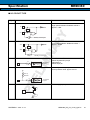
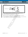
■ DESCRIPTION
MB96380 series is based on Fujitsu’s advanced 16FX architecture (16-bit with instruction pipeline for RISC-like
performance). The CPU uses the same instruction set as the established 16LX series enabling thus easy migration
of 16LX Software to the new 16FX products. In comparison with the previous generation, the 16FX products
include significantly improved performance even at the same operation frequency, a reduced power consumption
and a faster start-up time.
PR
EL
IM
IN
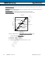
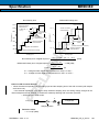
For highest processing speed at optimized power consumption an internal PLL can be selected to supply the
CPU with up to 56MHz operation frequency from an external 4MHz resonator. The result is a minimum instruction
cycle time of 17.8ns going together with excellent EMI behavior. An on-chip clock modulation circuit significantly
reduces emission peaks in the frequency spectrum. The emitted power is minimised by the on-chip voltage
regulator that reduces the internal CPU voltage. A flexible clock tree allows to select suitable operation frequencies
for peripheral resources independent of the CPU speed.
FME/EMDC- 2007-11-14MB96380_DS_cover.fm
Specification
PR
EL
IM
IN
AR
Y
MB96380 Series
2
FME/EMDC- 2007-11-14
MB96380_DS_cover.fm
Specification
MB96380
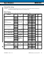
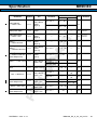
■ FEATURES
Feature
Description
Technology
• 0.18µm CMOS
• F2MC-16FX CPU
• Up to 56 MHz internal, 17.8 ns instruction cycle time
• 8-byte instruction execution queue
Y
• Optimized instruction set for controller applications (bit, byte, word and long-word
data types; 23 different addressing modes; barrel shift; variety of pointers)
CPU
• Signed multiply (16-bit × 16-bit) and divide (32-bit/16-bit) instructions available
AR
• On-chip PLL clock multiplier (x1..25, x1 when PLL stop)
• 3-16 MHz external quartz clock
• Up to 56MHz external clock for devices with fast clock input feature
• 32-100 kHz subsystem quartz clock
• 100kHz/2MHz internal RC clock for quick and safe startup, oscillator stop detection,
watchdog
System clock
IN
• Clock source selectable from main- and subclock oscillator (partnumber suffix “W”)
on-chip RC oscillator, independently for CPU and 2 clock domains of peripherals.
• Low Power Consumption - 13 operating modes : (different Run, Sleep, Timer modes,
Stop mode)
IM
• Clock modulator
On-chip voltage regula- • Internal voltage regulator supports reduced internal MCU voltage, offering low EMI
tor
and low power consumption figures
Low voltage reset
• Protects ROM content from unintended read-out
PR
EL
Code Security
Memory Patch Function
DMA
• Reset is generated when supply voltage is below minimum.
• Replaces ROM content
• Can also be used to implement embedded debug support
• Automatic transfer function independent of CPU, can be assigned freely to resources
• Fast Interrupt processing
Interrupts
• 8 programmable priority levels
• Non-Maskable Interrupt (NMI)
Timers
• Two independent clock timers (23-bit RC clock timer, 23-bit Main clock timer, 17-bit
Sub clock timer)
• Watchdog Timer
FME/EMDC- 2007-11-14
MB96300_DS_features.fm
3
MB96380 Series
Specification
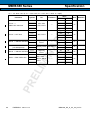
Feature
Description
• Supports CAN protocol version 2.0 part A and B
• ISO16845 certified
• Bit rates up to 1 Mbit/s
• 32 message objects
CAN
• Each message object has its own identifier mask
• Programmable FIFO mode (concatenation of message objects)
Y
• Maskable interrupt
• Disabled Automatic Retransmission mode for Time Triggered CAN applications
• Programmable loop-back mode for self-test operation
AR
• Full duplex USARTs (SCI/LIN)
• Wide range of baud rate settings using a dedicated reload timer
USART
• Special synchronous options for adapting to different synchronous serial protocols
• LIN functionality working either as master or slave LIN device
• Up to 400 kbit/s
I2C
• SAR-type
A/D converter
• 10-bit resolution
IN
• Master and Slave functionality, 8-bit and 10-bit addressing
A/D Converter Reference Voltage switch
EL
IM
• Signals interrupt on conversion end, single conversion mode, continuous conversion
mode, stop conversion mode, activation by software, external trigger or reload timer
• 2 independant positive A/D converter reference voltages available
• 16-bit wide
Reload Timers
• Prescaler with 1/21, 1/22, 1/23, 1/24, 1/25, 1/26 of peripheral clock frequency
• Event count function
Free Running Timers
• Signals an interrupt on overflow, supports timer clear upon match with Output
Compare (0, 4), Prescaler with 1, 1/21, 1/22, 1/23, 1/24, 1/25, 1/26 , 1/27 ,1/28 of
peripheral clock frequency
PR
• 16-bit wide
Input Capture Units
• Signals an interrupt upon external event
• Rising edge, falling edge or rising & falling edge sensitive
• 16-bit wide
Output Compare Units • Signals an interrupt when a match with 16-bit I/O Timer occurs
• A pair of compare registers can be used to generate an output signal.
4
FME/EMDC- 2007-11-14
MB96300_DS_features.fm
Specification
MB96380
Feature
Description
• 16-bit down counter, cycle and duty setting registers
• Interrupt at trigger, counter borrow and/or duty match
Programmable Pulse
Generator
• PWM operation and one-shot operation
• Internal prescaler allows 1, 1/4, 1/16, 1/64 of peripheral clock as counter clock and
Reload timer overflow as clock input
• Can be triggered by software or reload timer
• Stepper Motor Controller with integrated high current output drivers
Y
• Four high current outputs for each channel
AR
Stepper Motor Control- • Two synchronized 8/10-bit PWMs per channel
ler
• Internal prescaling for PWM clock: 1, 1/4, 1/5, 1/6, 1/8, 1/10, 1/12, 1/16 of peripheral
clock
• Separate power supply for high current output drivers
• LCD controller with up to 4 COM × 65 SEG
• Internal or external voltage generation
• Fixed 1/3 bias
IN
• Duty cycle: Selectable from options: 1/2, 1/3 and 1/4
• Programmable frame period
• Clock source selectable from three options (peripheral clock, subclock or RC
oscillator clock)
IM
LCD Controller
• On-chip drivers for internal divider resistors or external divider resistors
• On-chip data memory for display
• LCD display can be operated in Timer Mode
• Blank display: selectable
PR
EL
• All SEG, COM and V pins can be switched between general and specialized
purposes
• External divided resistors can be also used to shut off the current when LCD is
deactivated
• 8-bit PWM signal is mixed with tone frequency from 16-bit reload counter
Sound Generator
• PWM clock by internal prescaler: 1, 1/2, 1/4, 1/8 of peripheral clock
• Tone frequency: PWM frequency / 2 / (reload value + 1)
• Can be clocked either from sub oscillator (devices with partnumber suffix “W”),main
oscillator or from the RC oscillator
Real Time Clock
• Facility to correct oscillation deviation of Sub clock or RC oscillator clock (clock
calibration)
• Read/write accessible second/minute/hour registers
• Can signal interrupts every halfsecond/second/minute/hour/day
• Internal clock divider and prescaler provide exact 1s clock
FME/EMDC- 2007-11-14
MB96300_DS_features.fm
5
MB96380 Series
Specification
Feature
Description
• Edge sensitive or level sensitive
External Interrupts
• Interrupt mask and pending bit per channel
• Each available CAN channel RX has an external interrupt for wake-up
• Selected USART channels SIN have an external interrupt for wake-up
• Disabled after reset
• Once enabled, can not be disabled other than by reset.
• Level high or level low sensitive
• Pin shared with external interrupt 0.
• Up to 24-bit addresses
• 6 chip select signals
External bus interface
AR
• 8-bit or 16-bit bidirectional data
Y
Non Maskable Interrupt
• Multiplexed address/data lines
• Non-multiplexed address/data lines
• Wait state request
IN
• External bus master possible
• Timing programmable
• Monitors an external voltage and generates an interrupt in case of a voltage lower or
higher than the defined thresholds
• Threshold voltages defined externally or generated internally
EL
IM
Alarm comparators
• Status is readable, interrupts can be masked separately
• Virtually all external pins can be used as general purpose I/O
• All push-pull outputs (except when used as I2C SDA/SCL line)
• Bit-wise programmable as input/output or peripheral signal
I/O Ports
• Bit-wise programmable input enable
• Bit-wise programmable input levels (Automotive / CMOS-Schmitt trigger / TTL)
• Bit-wise programmable pull-up resistor
Package
PR
• Bit-wise programmable output driving strength for EMI optimization
• 120-pin plastic LQFP
• Supports automatic programming, Embedded AlgorithmTM*1
• Write/Erase/Erase-Suspend/Resume commands
• A flag indicating completion of the algorithm
• Number of erase cycles : 10,000 times
Flash Memory
• Data retention time : 20 years
• Erase can be performed on each sector individually
• Sector protection
• Flash Security feature to protect the content of the Flash
• Low voltage detection during Flash erase
6
FME/EMDC- 2007-11-14
MB96300_DS_features.fm
Specification
MB96380
Feature
: Embedded Algorithm is a trade mark of Advanced Micro Devices Inc.
PR
EL
IM
IN
AR
Y
*1
Description
FME/EMDC- 2007-11-14
MB96300_DS_features.fm
7
Specification
PR
EL
IM
IN
AR
Y
MB96380 Series
8
FME/EMDC- 2007-11-14
MB96300_DS_features.fm
Specification
MB96380
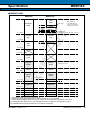
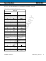
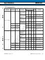
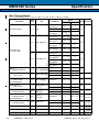
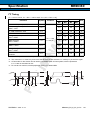
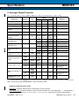
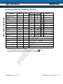
■ PRODUCT LINEUP
Features
MB96V300B
MB9638x
Product type
Evaluation sample
Flash product: MB96F38x
Mask ROM product: MB9638x
Product options
LVD persistently on / Single clock devices
RS
LVD can be disabled / Single clock devices
YW
LVD persistently on / Dual clock devices
Y
YS
LVD can be disabled / Dual clock devices
AR
RW
NA
satellite Flash / LVD persistently on / Single clock devices
HS
satellite Flash / LVD can be disabled / Single clock devices
TW
satellite Flash / LVD persistently on / Dual clock devices
HW
satellite Flash / LVD can be disabled / Dual clock devices
RAM
128kB
6kB
160kB
6kB
288kB
16kB
416kB
16kB
Main:
544kB,
Sat:
32kB
28kB
832kB
32kB
ROM/Flash memory emulation
by external RAM,
PR
EL
92kB internal RAM
Package
IM
Flash/
ROM
IN
TS
MB96384R, MB96384Y
MB96385R, MB96385Y
MB96F386R, MB96F386Y
MB96F387R, MB96F387Y
MB96F388T, MB96F388H
MB96F389R, MB96F389Y
BGA416
FPT-120P-M21
16 channels
7 channels
10 channels
5 channels
2 channels
1 channel
40 channels
16 channels
yes
Only for MB96F386R, MB96F386Y, MB96F387R, MB96F387Y
16-bit Reload
Timer
6 channels
4 channels + 1 channel (for PPG)
16-bit FreeRunning Timer
4 channels
2 channels
DMA
USART
I2C
A/D Converter
A/D Converter
Reference
Voltage switch
FME/EMDC- 2007-11-14
MB96380_DS_lineup.fm
9
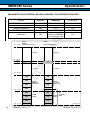
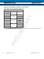
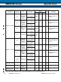
MB96380 Series
Specification
MB96V300B
MB9638x
16-bit Output
Compare
12 channels
4 channels
16-bit Input
Capture
12 channels
8 channels
16-bit
Programmable
Pulse Generator
20 channels
8 channels
CAN Interface
5 channels
2 channels
MB96384R, MB96384Y, MB96385R, MB96385Y: 1 channel
Stepping Motor
Controller
6 channels
5 channels
External
Interrupts
16 channels
Non-Maskable
Interrupt
2 channels
LCD Controller
4 COM x 72 SEG
Real Time Clock
Alarm comparator
2 channels
2 channels
MB96384R, MB96384Y, MB96385R, MB96385Y: 1 channel
Yes
6 signals
2 channels
Reset is generated when supply voltage is below minimum.
Yes
PR
On-chip RCoscillator
94 for part number with suffix "W", 96 for part number with suffix "S"
EL
IM
136
Low voltage reset
4 COM x 65 SEG
1
I/O Ports
Clock output
function
IN
2 channels
Chip select
8 channels
1 channel
Sound generator
External bus
interface
AR
Y
Features
10
FME/EMDC- 2007-11-14
MB96380_DS_lineup.fm
Specification
MB96380
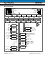
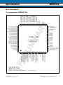
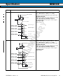
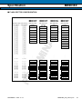
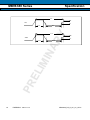
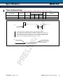
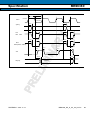
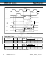
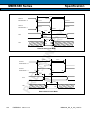
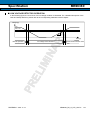
■ BLOCK DIAGRAM
External Bus
Interface
16FX
CPU
CKOT0, CKOT1
CKOTX0, CKOTX1
X0, X1
X0A, X1A
RSTX
MD0...MD2
NMI
Interrupt
Controller
Main Flash
Memory
Satellite Flash
Memory
AVCC
AVSS
AVRH
AVRL
AN0 ... AN15
ADTG
10-bit ADC
16 ch.
16-bit Reload
Timer
4 ch.
FRCK0
IN0 ... IN3
OUT0 ... OUT3
I/O Timer 0
ICU 0/1/2/3
OCU 0/1/2/3
TIN0 ... TIN3
FRCK1
IN4 ... IN7
USART
5 ch.
PR
EL
TOT0 ... TOT3
I/O Timer 1
ICU 4/5/6/7
Alarm
Comparator
2 ch.
16-bit PPG
8 ch.
Stepper
Motor
Controller
5 ch.
INT0 ... INT7
V0 ... V3
COM0 ... COM3
SEG0 ... SEG64
External
Interrupt
RAM
IN
SCL0
Peripheral Bus 2 (CLKP2)
I2C
1 ch.
Peripheral
Bus Bridge
IM
SDA0
Peripheral
Bus Bridge
Peripheral Bus 1 (CLKP1)
Watchdog
AR
16FX Core Bus (CLKB)
DMA
Controller
Real Time
Clock
Memory Patch
Unit
Clock &
Mode Controller
Y
AD00 ... AD15
A00 ... A23
ALE
RDX
WRLX, WRHX
HRQ
HAKX
RDY
ECLK
LBX, UBX
CS0 ... CS5
CAN
Interface
2 ch.
Boot ROM
Voltage
Regulator
VCC
VSS
C
TX0 ,TX1
RX0 , RX1
Sound
Generator
2 ch.
SGO0, SGO1
SGA1, SGA1
SIN0...SIN2,SIN4,SIN5
SOT0...SOT2,SOT4,SOT5
SCK0...SCK2,SCK4,SCK5
ALARM0
ALARM1
TTG0 ... TTG7
PPG0 ... PPG7
PWM1M0 ... PWM1M4
PWM1P0 ... PWM1P4
PWM2M0 ... PWM2M4
PWM2P0 ... PWM2P4
DVCC
DVSS
WOT
LCD
controller/
driver
FME/EMDC- 2007-11-14
MB96380_DS_block_diagram.fm
11
Specification
PR
EL
IM
IN
AR
Y
MB96380 Series
12
FME/EMDC- 2007-11-14
MB96380_DS_block_diagram.fm
Specification
MB96380
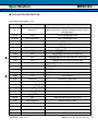
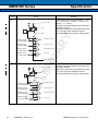
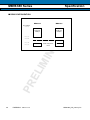
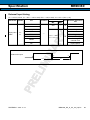
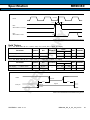
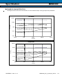
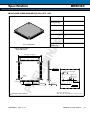
■ PIN ASSIGNMENTS
91
90 89 88 87 86 85 84 83 82 81 80 79 78 77 76 75 74 73 72 71 70 69 68 67 66 65 64 63 62 61
60
92
59
AR
93
94
95
96
97
98
99
100
101
102
LQFP - 120
IN
103
104
105
106
108
109
110
114
115
116
117
118
119
120
2
3
4
5
6
7
8
1) Devices with suffix W: X0A/X1A
Devices with suffix S: P04_0, P04_1
2) MB96384/5: Alarm1 not available
3) MB96384/5: TX1 resp. RX1 not available
4) AVRH2 only available for MB96F386 and MB96F387
FME/EMDC- 2007-11-14
54
53
52
51
50
49
48
45
44
43
42
41
40
39
38
37
36
35
34
33
32
31
9 10 11 12 13 14 15 16 17 18 19 20 21 22 23 24 25 26 27 28 29 30
Vss
C
P03_7/INT1/SIN1/CS0/A20/SEG40
P13_0/INT2/SOT1/CS1/A21/SEG41
P13_1/INT3/SCK1/CS2/A22/SEG42
P13_2/PPG0/TIN0/FRCK1/CS3/A23/SEG43
P13_3/PPG1/TOT0/WOT/UBX/SEG44
P13_4/SIN0/INT6/SEG45
P13_5/SOT0/ADTG/INT7/SEG46
P13_6/SCK0/CKOTX0/LBX/SEG47
P13_7/PPG2/CKOT0/CS4/SEG48
P04_4/PPG3/SDA0
P04_5/PPG4/SCL0
P06_0/AN0/SCK5/IN2_R/SEG49
P06_1/AN1/SOT5/IN3_R/SEG50
P06_2/AN2/INT5/SIN5/SEG51
P06_3/AN3/FRCK0/SEG52
P06_4/AN4/IN0/TTG0/TTG4/SEG53
P06_5/AN5/IN1/TTG1/TTG5/SEG54
P06_6/AN6/TIN1/IN4_R/SEG55
P06_7/AN7/TOT1//IN5_R/SEG56
AVcc
AVRH
1
55
AVRL/AVRH2
AVss
P05_0/AN8/ALARM0/SEG57
2) P05_1/AN9/ALARM1/SEG58
P05_2/AN10/OUT2/SGO1/SEG59
P05_3/AN11/OUT3/SGA1/SEG60
Vcc
113
56
Vcc
P10_3/PWM2M4/PPG7
P10_2/PWM2P4/SCK2/PPG6
P10_1/PWM1M4/SOT2/TOT3
P10_0/PWM1P4/SIN2/TIN3
P09_7/PWM2M3
DVss
DVcc
P09_6/PWM2P3
P09_5/PWM1M3
P09_4/PWM1P3
P09_3/PWM2M2
P09_2/PWM2P2
P09_1/PWM1M2
P09_0/PWM1P2
P08_7/PWM2M1
P08_6/PWM2P1
P08_5/PWM1M1
DVss
DVcc
P08_4/PWM1P1
P08_3/PWM2M0
P08_2/PWM2P0
P08_1/PWM1M0
P08_0/PWM1P0
P05_7/AN15/TOT2/SGA1_R/SEG64
P05_6/AN14/TIN2/SGO1_R/SEG63
P05_5/AN13/TX1/SEG62 3)
P05_4/AN12/RX1/INT2_R/SEG61 3)
Vss
4)
112
57
46
IM
111
58
47
Package code (mold)
FPT-120P-M21
107
PR
EL
Vss
P00_3/INT6_R/A00/CS3_R/SEG15
P00_4/INT7_R/ALE/SEG16
P00_5/TTG2/TTG6/IN6/RDX/SEG17
P00_6/TTG3/IN7/WRLX/TTG8/SEG18
P00_7/SGO0/ECLK/SEG19
P01_0/SGA0/AD00/SEG20
P01_1/OUT0/CKOT1/AD01/SEG21
P01_2/OUT1/CKOTX1/AD02/SEG22
P01_3/PPG5/AD03/SEG23
P01_4/AD04/SIN4/SEG24
P01_5/AD05/SOT4/SEG25
P01_6/AD06/SCK4/SEG26
P01_7/CKOTX1_R/AD07/SEG27
P02_0/CKOT1_R/AD08/SEG28
P02_1/IN6_R/AD09/SEG29
P02_2/IN7_R/AD10/SEG30
P02_3/SGO0_R/AD11/SEG31
P02_4/SGA0_R/AD12/SEG32
P02_5/OUT0_R/AD13/SEG33
P02_6/OUT1_R/AD14/SEG34
P02_7/PPG5_R/AD15/SEG35
P03_0/V0/A16/SEG36
P03_1/V1/A17/SEG37
P03_2/V2/A18/SEG38
P03_3/V3/A19/SEG39
P03_4/INT4/RX0
P03_5/TX0
P03_6/NMI/INT0
Vcc
Y
Vcc
P00_2/INT5_R/RDY/SEG14
P00_1/INT4_R/WRHX/SEG13
P00_0/INT3_R/HAKX/SEG12
P12_7/INT1_R/HRQ/SEG11
P12_6/TOT2_R/A15/SEG10
P12_5/TIN2_R/A14/SEG9
P12_4/OUT3_R/A13/SEG8
P12_3/OUT2_R/A12/SEG7
P12_2/TOT1_R/A11/SEG6
P12_1/TIN1_R/A10/SEG5
P12_0/IN1_R/A09/SEG4
P11_7/IN0_R/A08/SEG3
P11_6/FRCK0_R/A07/SEG2
P11_5/PPG4_R/A06/SEG1
P11_4/PPG3_R/A05/SEG0
P11_3/PPG2_R/A04/COM3
P11_2/PPG1_R/A03/COM2
P11_1/PPG0_R/A02/COM1
P11_0/A01/COM0/CS5
RSTX
X1A/P04_1 1)
X0A/P04_0 1)
Vss
X1
X0
MD2
MD1
MD0
Vss
Pin assignment of MB96(F)38x
(FPT-120P-M21)
MB96380_DS_pin_assignement.fm
13
Specification
PR
EL
IM
IN
AR
Y
MB96380 Series
14
FME/EMDC- 2007-11-14
MB96380_DS_pin_assignement.fm
Specification
MB96380
■ PIN FUNCTION DESCRIPTION
Pin Function description (1 / 3)
Feature
Description
ADn
External bus
External bus interface (nonmultiplexed mode) data input/
output. External bus interface (multiplexed mode) address/
data input/output
ADTG
ADC
A/D converter trigger input
ALARMn
Alarm comparator
Alarm Comparator n input
ALE
External bus
External bus Address Latch Enable output
An
External bus
External bus (non-multiplexed mode) address output
ANn
ADC
A/D converter channel n input
AVCC
Supply
AVRH
ADC
A/D converter high reference voltage input
AVRH2
ADC
Alternative A/D converter high reference voltage input
AVRL
ADC
AVSS
Supply
C
Voltage regulator
CKOTn
Clock output function
Clock Output function n output
CKOTXn
Clock output function
Clock Output Function n inverted output
COMn
LCD
LCD COM pins
AR
IN
Analogue circuits power supply
A/D converter low reference voltage input
Analogue circuits power supply
IM
Internally regulated power supply stabilization capacitor pin.
PR
EL
ECLK
Y
Pin name
External bus
External bus clock output
External bus
External bus chip select n output
Free Running Timer
Free Running Timer n input
External bus
External bus Hold Acknowlegde
External bus
External bus Hold Request
ICU
Input Capture Unit n input
ICU
Relocated Input Capture Unit n input
External Interrupt
External Interrupt n input
INTn_R
External Interrupt
Relocated External Interrupt n input
LBX
External bus
External Bus Interface Lower Byte select strobe output
MDn
Core
Input pins for specifying the operating mode.
NMI
External Interrupt
Non-Maskable Interrupt input
CSn
FRCKn
HAKX
HRQ
INn
INn_R
INTn
FME/EMDC- 2007-11-14
MB96300_DS_pin_function_desc.fm
15
MB96380 Series
Specification
Pin Function description (2 / 3)
Feature
Description
OUTn
OCU
Output Compare Unit n waveform output
OUTn_R
OCU
Relocated Output Compare Unit n waveform output
PPGn
PPG
Programmable Pulse Generator n output
PWMn
SMC
SMC PWM high current
RDX
External bus
External bus interface read strobe output
RDY
External bus
External bus interface external wait state request input
RSTX
Core
Reset input
RXn
CAN
SCKn
USART
SCLn
I2C
SDAn
I2C
SEGn
LCD
SGA
Sound Generator
SGO
Sound Generator
SGA_R
Sound Generator
SGO_R
Sound Generator
SG sound/tone output
SINn
USART
USART n serial data input
SOTn
USART
USART n serial data output
TINn
Reload Timer
Reload Timer n event input
TINn_R
Reload Timer
Relocated Reload Timer n event input
TOTn
Reload Timer
Reload Timer n output
TOTn_R
Reload Timer
Relocated Reload Timer n output
AR
CAN interface n RX input
USART n serial clock input/output
I2C interface n clock I/O input/output
EL
IM
IN
I2C interface n serial data I/O input/output
LCD segment n
SG amplitude output
SG sound/tone output
SG amplitude output
PPG
Programmable Pulse Generator n trigger input
CAN
CAN interface n TX output
External bus
External Bus Interface Upper Byte select strobe output
LCD
LCD voltage references
VCC
Supply
Power supply
VSS
Supply
Power supply
WOT
RTC
Real Timer clock output
WRHX
External bus
External bus High byte Write strobe output
TXn
UBX
Vn
16
PR
TTGn
Y
Pin name
FME/EMDC- 2007-11-14
MB96300_DS_pin_function_desc.fm
Specification
MB96380
Pin Function description (3 / 3)
Feature
Description
WRLX
External bus
External bus Low byte Write strobe output
X0
Clock
Oscillator input
X0A
Clock
Subclock Oscillator input (only for devices with suffix "W")
X1
Clock
Oscillator output
X1A
Clock
Subclock Oscillator output (only for devices with suffix "W")
PR
EL
IM
IN
AR
Y
Pin name
FME/EMDC- 2007-11-14
MB96300_DS_pin_function_desc.fm
17
Specification
PR
EL
IM
IN
AR
Y
MB96380 Series
18
FME/EMDC- 2007-11-14
MB96300_DS_pin_function_desc.fm
Specification
MB96380
■ PIN CIRCUIT TYPE
FPT-120P-M21
Circuit
type
1
Supply
2
C-pin
3 to 11
J
12,13
N
14 to 21
K
22
Supply
23
G
24 to 25
Supply
26 to 29
K
30,31
Supply
32 to 35
K
36 to 40
M
41,42
Supply
43 to 52
M
53,54
Supply
55 to 59
M
60, 61
Supply
62 to 64
C
65, 66
A
67
Supply
68,69
B1)
68,69
H2)
70
E
71 to 89
J
PR
EL
IM
IN
AR
Y
Pin no.
1)
Devices with suffix
”W”
2) Devices without
suffix ”W”
FME/EMDC- 2007-11-14
MB96380_DS_pin_circuit_type.fm
19
MB96380 Series
Specification
Circuit
type
90 to 91
Supply
92 to 112
J
113 to
116
L
117 to
119
H
120
Supply
AR
Pin no.
Y
FPT-120P-M21
1)
PR
EL
IM
IN
Devices with suffix
”W”
2) Devices without
suffix ”W”
20
FME/EMDC- 2007-11-14
MB96380_DS_pin_circuit_type.fm
Specification
MB96380
■ I/O CIRCUIT TYPE
Type
Circuit
Remarks
A
X1
Oscillation circuit
High-speed oscillation feedback resistor =
approx. 1 MΩ
Xout
Y
X0
B
X1A
Xout
Oscillation circuit
Low-speed oscillation feedback resistor =
approx. 10 MΩ
IN
X0A
AR
Standby control signal
Standby control signal
IM
C
R
Hysteresis
inputs
PR
EL
E
Mask ROM and EVA device:
CMOS Hysteresis input pin
Flash device:
CMOS input pin
CMOS Hysteresis input pin
Pull-up resistor value: approx. 50 kΩ
Pull-up
Resistor
R
F
FME/EMDC- 2007-11-14
Hysteresis
inputs
Power supply input protection circuit
MB96380_DS_pin_circuit_type.fm
21
MB96380 Series
Type
Specification
Circuit
Remarks
H
CMOS level output (programmable IOL = 5mA,
IOH = -5mA and IOL = 2mA, IOH = -2mA).
2 different CMOS hysteresis inputs with input
shutdown function.
Automotive input with input shutdown function.
TTL input with input shutdown function.
Programmable pull-up registor: 50kΩ approx.
pull-up control
Pout
Y
Nout
R
AR
Hysteresis input
Standby control
for input shutdown
Hysteresis input
Standby control
for input shutdown
Automotive inputs
Standby control
for input shutdown
TTL input
IN
Standby control
for input shutdown
J
EL
IM
pull-up control
Pout
Nout
R
Standby control
for input shutdown
PR
Standby control
for input shutdown
22
Hysteresis input
Hysteresis input
Standby control
for input shutdown
Automotive inputs
Standby control
for input shutdown
TTL input
FME/EMDC- 2007-11-14
CMOS level output (programmable IOL = 5mA,
IOH = -5mA and IOL = 2mA, IOH = -2mA).
2 different CMOS hysteresis inputs with input
shutdown function.
Automotive input with input shutdown function)
TTL input with input shutdown function.
Programmable pull-up registor: 50kΩ approx.
SEG or COM output.
SEG, COM output
MB96380_DS_pin_circuit_type.fm
Specification
MB96380
Type
Circuit
Remarks
K
CMOS level output (programmable IOL = 5mA,
IOH = -5mA and IOL = 2mA, IOH = -2mA).
2 different CMOS hysteresis inputs with input
shutdown function.
Automotive input with input shutdown function)
TTL input with input shutdown function.
Programmable pull-up registor: 50kΩ approx.
Analogue input.
SEG output.
pull-up control
Pout
Nout
Y
R
AR
Hysteresis input
Standby control
for input shutdown
Standby control
for input shutdown
Hysteresis input
Standby control
for input shutdown
Automotive inputs
Standby control
for input shutdown
TTL input
IN
Analog input
SEG output
L
IM
pull-up control
Pout
PR
EL
Nout
CMOS level output (programmable IOL = 5mA,
IOH = -5mA and IOL = 2mA, IOH = -2mA).
2 different CMOS hysteresis inputs with input
shutdown function.
Automotive input with input shutdown function)
TTL input with input shutdown function.
Programmable pull-up registor: 50kΩ approx.
Analogue input.
SEG output.
R
Standby control
for input shutdown
Hysteresis input
Standby control
for input shutdown
Hysteresis input
Standby control
for input shutdown
Automotive intputs
Standby control
for input shutdown
TTL intput
Analog input
SEG output
Vx intput
FME/EMDC- 2007-11-14
MB96380_DS_pin_circuit_type.fm
23
MB96380 Series
Circuit
Remarks
M
CMOS level output (programmable IOL = 5mA,
IOH = -5mA and IOL = 2mA, IOH = -2mA, IOL =
30mA, IOH = -30mA).
2 different CMOS hysteresis inputs with input
shutdown function.
Automotive input with input shutdown function
TTL input with input shutdown function.
Programmable pull-up registor: 50kΩ approx.
pull-up control
Pout
Nout
Y
Type
Specification
R
AR
Hysteresis input
Standby control
for input shutdown
Hysteresis input
Standby control
for input shutdown
Automotive inputs
Standby control
for input shutdown
TTL input
IN
Standby control
for input shutdown
SEG, COM output
EL
IM
N
pull-up control
Pout
CMOS level output (IOL = 3mA, IOH = -3mA)
2 different CMOS hysteresis inputs with input
shutdown function.
Automotive input with input shutdown function
TTL input with input shutdown function.
Programmable pull-up registor: 50kΩ approx.
Nout
R
Standby control
for input shutdown
PR
Standby control
for input shutdown
24
Hysteresis input
Hysteresis input
Standby control
for input shutdown
Automotive inputs
Standby control
for input shutdown
TTL input
FME/EMDC- 2007-11-14
MB96380_DS_pin_circuit_type.fm
Specification
MB96380
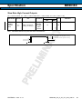
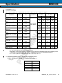
■ MEMORY MAP
MB96V300
MB96(F)38x
ff.ffff
User
ROM
Emulation
ROM
Main Flash
external
Bus
0f.e000
DSU
area
internal
RAM
01.0000
internal
RAM
RAM availability and mapping
depending on device.
ROM/RAM
-Mirror
PR
EL
00.8000
ROM/RAM
-Mirror
Boot-ROM
IM
02.0000
Satellite Flash
(available on devices with suffix “T” and “H”)
IN
0f.0000
external
RAM
Sat RCB ***
external
Bus
10.0000
0e.0000
Main RCB ***
AR
de.0000
Small Sectors
Y
df.007f
df.0000
de.002f
de.0000
Start address of
User ROM area and
number of small sector
depends on the device
internal
RAM
internal
RAM
RAMSTART**
00.1200
Reserved
ext. bus
ext. bus
Peripheral
Peripheral
GPR*
DMA
ext. bus
Peripheral
GPR*
DMA
ext. bus
Peripheral
00.0c00
External Bus end address**
00.0380
00.0180
00.0100
00.00f0
00.0000
* Unused GPR banks can be used as RAM area.
** Please refer to the table “RAMSTART for different RAM sizes” on the next page
*** ROM Configuration Block (RCB) must not be used for other purposes than described in the manual
The external Bus area DMA area are only available if the device contains the corresponding resource.
The available RAM and ROM area depends on the device configuration.
FME/EMDC- 2007-11-14
MB96380_DS_memory.fm
25
MB96380 Series
Specification
■ RAMSTART AND EXTERNAL BUS END ADDRESS FOR DIFFERENT RAM SIZES
RAM size
RAMSTART
End address of external bus area
MB96384
6kB
6A40
69FF
MB96385
8kB
6240
61FF
MB96F386, MB96F387
16kB
4240
41FF
MB96F388
28kB
1240
11FF
MB96F389
32kB
1240
additionnal 4kB RAM:
0x01.8000-0x01.9000
11FF
01.9000
01.8000
4kB
AR
(RAM-Mirroring on)
EL
IM
unused
32kB
IN
32kB
default
02.0000 (RAM-Mirroring off)
Y
Devices
4kB
unused
01.0000
8kB
8kB
00.8000
00.1200
26
ROMmirroring
(bank Fx)
8kB
8kB
8kB
4kB
4kB
8kB
8kB
8kB
28kB
RAM
8kB
8kB
8kB
4kB
4kB
FME/EMDC- 2007-11-14
unused
8kB
PR
8kB
unused
ROMmirroring
(bank Fx)
28kB
RAM
32k
continues
RAM
RAMSTART*
MB96380_DS_memory.fm
Specification
MB96380
■ FLASH SECTOR CONFIGURATION
MB96F386R
MB96F386Y
3F:0000h
3E:FFFFh
FE:0000h
FD:FFFFh
3E:0000h
3D:FFFFh
FD:0000h
FC:FFFFh
3D:0000h
3C:FFFFh
FC:0000h
FB:FFFFh
3C:0000h
3B:FFFFh
3B:0000h
3A:FFFFh
FA:0000h
F9:FFFFh
3A:0000h
39:FFFFh
F9:0000h
F8:FFFFh
39:0000h
38:FFFFh
F8:0000h
F7:FFFFh
38:0000h
37:FFFFh
F7:0000h
F6:FFFFh
37:0000h
36:FFFFh
F6:0000h
F5:FFFFh
36:0000h
35:FFFFh
F5:0000h
F4:FFFFh
35:0000h
34:FFFFh
F4:0000h
F3:FFFFh
34:0000h
33:FFFFh
F3:0000h
F2:FFFFh
33:0000h
32:FFFFh
F2:0000h
F1:FFFFh
32:0000h
31:FFFFh
F1:0000h
F0:FFFFh
31:0000h
30:FFFFh
F0:0000h
30:0000h
.
.
.
.
E0:FFFFh
.
.
.
.
20:FFFFh
E0:0000h
.
.
8k steps
.
.
DF:7FFFh
DF:6000h
DF:5FFFh
DF:4000h
DF:3FFFh
DF:2000h
DF:1FFFh
DF:0000h
20:0000h
.
.
8k steps
.
.
1F:7FFFh
1F:6000h
1F:5FFFh
1F:4000h
1F:3FFFh
1F:2000h
1F:1FFFh
1F:0000h
.
.
8k steps
.
.
DE:7FFFh
DE:6000h
DE:5FFFh
DE:4000h
DE:3FFFh
DE:2000h
DE:1FFFh
DE:0000h
Main Flash size
576kByte
Main Flash size
832kByte
S39 - 64K
S39 - 64K
S39 - 64K
S39 - 64K
S38 - 64K
S38 - 64K
S38 - 64K
S38 - 64K
S37 - 64K
S37 - 64K
S37 - 64K
S37 - 64K
S36 - 64K
S36 - 64K
S36 - 64K
S36 - 64K
S35 - 64K
S35 - 64K
S34 - 64K
S34 - 64K
S33 - 64K
S33 - 64K
S32 - 64K
S32 - 64K
S35 - 64K
S34 - 64K
.
.
.
.
PR
EL
FB:0000h
FA:FFFFh
Main Flash size
416kByte
Y
FF:0000h
FE:FFFFh
MB96F389R
MB96F389Y
Main Flash size
288kByte
AR
3F:FFFFh
MB96F388T
MB96F388H
S31 - 64K
S30 - 64K
S29 - 64K
S28 - 64K
IN
FF:FFFFh
IM
Alternative mode Flash memory
CPU address mode address
MB96F387R
MB96F387Y
SA3 - 8K
SA2 - 8K
SA1 - 8K
SA0 - 8K
.
.
.
.
.
.
.
.
.
.
.
.
SA3 - 8K
SA2 - 8K
SA1 - 8K
SA0 - 8K
SA3 - 8K
SA2 - 8K
SA1 - 8K
SA0 - 8K
SA3 - 8K
SA2 - 8K
SA1 - 8K
SA0 - 8K
SB3 - 8K
SB2 - 8K
SB1 - 8K
SB0 - 8K
SB3 - 8K
SB2 - 8K
SB1 - 8K
SB0 - 8K
.
.
8k steps
.
.
1E:7FFFh
1E:6000h
1E:5FFFh
1E:4000h
1E:3FFFh
1E:2000h
1E:1FFFh
1E:0000h
FME/EMDC- 2007-11-14
MB96380_DS_memory.fm
27
MB96380 Series
Specification
■ ROM CONFIGURATION
MB96384
MB96385
ROM size
128kByte
ROM size
128kByte
CPU address
Y
FF:FFFFh
DF:7FFFh
AR
FD:0000h
32K
DF:007Eh
ROM configuration
block
PR
EL
IM
IN
DF:0000h
28
FME/EMDC- 2007-11-14
MB96380_DS_memory.fm
Specification
MB96380
■ PARALLEL PROGRAMMING FLASH MEMORY CONTROL SIGNALS
Flash memory control signals (MD[2:0] = 111)
MB96F38X
Pin number
Normal function
Flash memory mode
32
P05_4
TMODIX
33 to 35
P13_3 to P13_5
AQ19 to AQ21
3
P03_7
RY/BY
8 to 9
P13_4 to P13_5
AQ8 to AQ9
12 to 13
P04_4 to P04_5
AQ10 to AQ11
10 to 11
P13_6 to P13_7
AQ12 to AQ13
14 to 15
P06_0 to P06_1
AQ22 to AQ23
26 to 27
P05_0 to P05_1
AQ14 to AQ15
28
P05_2
ATD
62
MD0
VDA9
63
MD1
VDRS
64
MD2
16
P06_2
17
P06_3
18
P06_4
ATD2
EQ2
PR
EL
FRST
P00_0 to P00_7
DQ0 to DQ7
97 to 104
P01_0 to P01_7
DQ8 to DQ15
105 to 112
P02_0 to P02_7
AQ0 to AQ7
113
P03_0
AQ16
P03_1
CE
P03_2
OE
P03_3
WE
117 to 118
P03_4 to P03_5
AQ17 to AQ18
119
P03_6
BYTE
115
116
AR
IN
IM
VDOE
87 to 89, 92 to
96
114
Y
LQFP
FME/EMDC- 2007-11-14
MB96380_DS_memory.fm
29
MB96380 Series
Specification
■ SERIAL PROGRAMMING COMMUNICATION INTERFACE
USART pins for Flash serial programming (MD[2:0] = 010)
MB96F38x
Pin number
USART Number
Normal function
LQFP-120
USART0
SOT0
10
SCK0
3
SIN1
4
USART1
SOT1
5
SCK1
56
SIN2
USART2
58
SOT2
IN
57
Y
9
SIN0
AR
8
SCK2
PR
EL
IM
Note: For handshaking pin, please use for this device the default pin P00_1. If any other pin is required, please
contact the Flash programmer device vendor.
30
FME/EMDC- 2007-11-14
MB96380_DS_memory.fm
Specification
MB96380
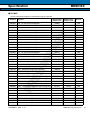
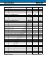
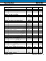
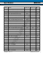
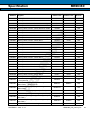
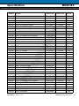
■ I/O MAP
All non-mentionned registers in the address map are reserved.
Abbreviation
8-bit access
Abbreviation
16-bit access
Register
000000H
P00 - I/O Port Port Data Register
PDR00
RW
000001H
P01 - I/O Port Port Data Register
PDR01
RW
000002H
P02 - I/O Port Port Data Register
PDR02
RW
000003H
P03 - I/O Port Port Data Register
PDR03
RW
000004H
P04 - I/O Port Port Data Register
PDR04
RW
000005H
P05 - I/O Port Port Data Register
PDR05
RW
000006H
P06 - I/O Port Port Data Register
PDR06
RW
000008H
P08 - I/O Port Port Data Register
000009H
P09 - I/O Port Port Data Register
00000AH
P10 - I/O Port Port Data Register
00000BH
P11 - I/O Port Port Data Register
00000CH
P12 - I/O Port Port Data Register
00000DH
P13 - I/O Port Port Data Register
000018H
ADC - Control Status register 0 Low
000019H
ADC - Control Status register 0 High
00001AH
ADC - Data Register 0 Low
00001BH
ADC - Data Register 0 High
00001CH
ADC - Setting Register 0 Low
00001DH
ADC - Setting Register 0 High
00001EH
ADC - Extended Configuration Register
000020H
FRT0 - Data register of free-running timer
000021H
FRT0 - Data register of free-running timer
000022H
FRT0 - Control status register of free-running timer
TCCSL0
000023H
FRT0 - Control status register of free-running timer
TCCSH0
000024H
FRT1 - Data register of free-running timer
000025H
FRT1 - Data register of free-running timer
000026H
FRT1 - Control status register of free-running timer
TCCSL1
000027H
FRT1 - Control status register of free-running timer
TCCSH1
RW
000028H
OCU0 - Output Compare Control Status
OCS0
RW
000029H
OCU1 - Output Compare Control Status
OCS1
RW
00002AH
OCU0 - Compare Register
00002BH
OCU0 - Compare Register
00002CH
OCU1 - Compare Register
00002DH
OCU1 - Compare Register
IN
AR
Y
Address
PDR08
RW
PDR09
RW
PDR10
RW
PDR11
RW
PDR12
RW
PDR13
RW
ADCSL
IM
ADCS
ADCSH
ADCRL
PR
EL
FME/EMDC- 2007-11-14
Access
RW
RW
ADCR
ADCRH
R
R
ADSR
RW
RW
ADECR
RW
TCDT0
RW
RW
TCCS0
RW
RW
TCDT1
RW
RW
TCCS1
OCCP0
RW
RW
RW
OCCP1
RW
RW
MB96380_DS_memory.fm
31
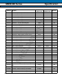
MB96380 Series
32
Specification
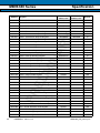
Abbreviation
8-bit access
Abbreviation
16-bit access
Address
Register
00002EH
OCU2 - Output Compare Control Status
OCS2
RW
00002FH
OCU3 - Output Compare Control Status
OCS3
RW
000030H
OCU2 - Compare Register
000031H
OCU2 - Compare Register
000032H
OCU3 - Compare Register
000033H
OCU3 - Compare Register
000040H
ICU0/ICU1 - Control Status Register
ICS01
RW
000041H
ICU0/ICU1 - Edge register
ICE01
RW
000042H
ICU0 - Capture Register
000043H
ICU0 - Capture Register
000044H
ICU1 - Capture Register
000045H
ICU1 - Capture Register
000046H
ICU2/ICU3 - Control Status Register
000047H
ICU2/ICU3 - Edge register (internal version)
000048H
ICU2 - Capture Register
000049H
ICU2 - Capture Register
00004AH
ICU3 - Capture Register
00004BH
ICU3 - Capture Register
00004CH
OCCP2
Access
RW
RW
OCCP3
RW
Y
RW
AR
IPCPL0
IPCP0
IPCPH0
IN
IPCPL1
R
R
IPCP1
R
IPCPH1
R
ICS23
RW
ICE23
RW
IPCPL2
IPCP2
IPCPH2
IPCPL3
R
R
IPCP3
R
R
ICU4/ICU5 - Control Status Register
ICS45
RW
00004DH
ICU4/ICU5 - Edge register
ICE45
RW
00004EH
ICU4 - Capture Register
IPCPL4
00004FH
ICU4 - Capture Register
IPCPH4
000050H
ICU5 - Capture Register
IPCPL5
000051H
ICU5 - Capture Register
IPCPH5
R
000052H
ICU6/ICU7 - Control Status Register
ICS67
RW
000053H
ICU6/ICU7 - Edge register
ICE67
RW
000054H
ICU6 - Capture Register
IPCPL6
000055H
ICU6 - Capture Register
IPCPH6
000056H
ICU7 - Capture Register
IPCPL7
000057H
ICU7 - Capture Register
IPCPH7
R
000058H
EXTINT0 - External Interrupt Enable Register
ENIR0
RW
000059H
EXTINT0 - External Interrupt Interrupt request Register
EIRR0
RW
00005AH
EXTINT0 - External Interrupt Level Select
ELVRL0
00005BH
EXTINT0 - External Interrupt Level Select
ELVRH0
000060H
RLT0 - Timer Control Status Register Low
TMCSRL0
000061H
RLT0 - Timer Control Status Register High
TMCSRH0
PR
EL
IM
IPCPH3
FME/EMDC- 2007-11-14
IPCP4
R
R
IPCP5
IPCP6
R
R
R
IPCP7
ELVR0
R
RW
RW
TMCSR0
RW
RW
MB96380_DS_memory.fm
Specification
MB96380
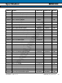
Abbreviation
8-bit access
Abbreviation
16-bit access
Access
RLT0 - Reload Register Low
TMRLR0
TMR0
RW
000063H
RLT0 - Reload Register High
TMRHR0
000064H
RLT1 - Timer Control Status Register Low
TMCSRL1
000065H
RLT1 - Timer Control Status Register High
TMCSRH1
000066H
RLT1 - Reload Register Low
TMRLR1
000067H
RLT1 - Reload Register High
TMRHR1
000068H
RLT2 - Timer Control Status Register Low
TMCSRL2
000069H
RLT2 - Timer Control Status Register High
TMCSRH2
00006AH
RLT2 - Reload Register Low
00006BH
RLT2 - Reload Register High
00006CH
RLT3 - Timer Control Status Register Low
00006DH
RLT3 - Timer Control Status Register High
00006EH
RLT3 - Reload Register Low
00006FH
RLT3 - Reload Register High
000070H
RLT6 - Timer Control Status Register Low (dedic.
RLT for PPG)
TMCSRL6
000071H
RLT6 - Timer Control Status Register High (dedic.
RLT for PPG)
TMCSRH6
000072H
RLT6 - Reload Register Low (dedic. RLT for PPG)
TMRLR6
000073H
RLT6 - Reload Register High (dedic. RLT for PPG)
TMRHR6
000074H
PPG3-PPG0 - General Control register 1 Low
GCN1L0
000075H
PPG3-PPG0 - General Control register 1 High
GCN1H0
000076H
PPG3-PPG0 - General Control register 2 Low
GCN2L0
000077H
PPG3-PPG0 - General Control register 2 High
GCN2H0
000078H
PPG0 - Timer register
000079H
PPG0 - Timer register
00007AH
PPG0 - Period setting register
00007BH
PPG0 - Period setting register
00007CH
PPG0 - Duty cycle register
00007DH
PPG0 - Duty cycle register
00007EH
PPG0 - Control status register
PCNL0
00007FH
PPG0 - Control status register
PCNH0
000080H
PPG1 - Timer register
000081H
PPG1 - Timer register
000082H
PPG1 - Period setting register
000083H
PPG1 - Period setting register
000084H
PPG1 - Duty cycle register
TMRLR2
TMCSR1
TMCSRL3
TMR1
TMCSR2
RW
RW
TMR2
RW
RW
TMCSR3
RW
RW
TMR3
TMRHR3
IM
RW
RW
TMCSRH3
TMRLR3
RW
RW
TMRHR2
PR
EL
FME/EMDC- 2007-11-14
RW
Y
000062H
AR
Register
IN
Address
RW
RW
TMCSR6
RW
RW
TMR6
RW
RW
GCN10
RW
RW
GCN20
RW
RW
PTMR0
R
R
PCSR0
W
W
PDUT0
W
W
PCN0
RW
RW
PTMR1
R
R
PCSR1
W
W
PDUT1
W
MB96380_DS_memory.fm
33
MB96380 Series
34
Specification
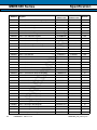
Abbreviation
8-bit access
Address
Register
000085H
PPG1 - Duty cycle register
000086H
PPG1 - Control status register
PCNL1
000087H
PPG1 - Control status register
PCNH1
000088H
PPG2 - Timer register
000089H
PPG2 - Timer register
00008AH
PPG2 - Period setting register
00008BH
PPG2 - Period setting register
00008CH
PPG2 - Duty cycle register
00008DH
PPG2 - Duty cycle register
00008EH
PPG2 - Control status register
00008FH
PPG2 - Control status register
000090H
PPG3 - Timer register
000091H
PPG3 - Timer register
000092H
PPG3 - Period setting register
000093H
PPG3 - Period setting register
000094H
PPG3 - Duty cycle register
000095H
PPG3 - Duty cycle register
000096H
PPG3 - Control status register
000097H
PPG3 - Control status register
PCNH3
000098H
PPG7-PPG4 - General Control register 1 Low
GCN1L1
000099H
PPG7-PPG4 - General Control register 1 High
GCN1H1
00009AH
PPG7-PPG4 - General Control register 2 Low
GCN2L1
00009BH
PPG7-PPG4 - General Control register 2 High
GCN2H1
00009CH
PPG4 - Timer register
00009DH
PPG4 - Timer register
00009EH
PPG4 - Period setting register
00009FH
PPG4 - Period setting register
0000A0H
PPG4 - Duty cycle register
0000A1H
PPG4 - Duty cycle register
0000A2H
PPG4 - Control status register
PCNL4
0000A3H
PPG4 - Control status register
PCNH4
0000A4H
PPG5 - Timer register
0000A5H
PPG5 - Timer register
0000A6H
PPG5 - Period setting register
0000A7H
PPG5 - Period setting register
0000A8H
PPG5 - Duty cycle register
Access
W
PCN1
RW
RW
PTMR2
R
R
AR
Y
PCSR2
PCNL2
IN
W
W
PDUT2
W
W
PCN2
PCNH2
EL
IM
PR
FME/EMDC- 2007-11-14
Abbreviation
16-bit access
RW
RW
PTMR3
R
R
PCSR3
W
W
PDUT3
W
W
PCNL3
PCN3
RW
RW
GCN11
RW
RW
GCN21
RW
RW
PTMR4
R
R
PCSR4
W
W
PDUT4
W
W
PCN4
RW
RW
PTMR5
R
R
PCSR5
W
W
PDUT5
W
MB96380_DS_memory.fm
Specification
Address
Register
0000A9H
PPG5 - Duty cycle register
MB96380
Abbreviation
8-bit access
Abbreviation
16-bit access
Access
W
0000AAH PPG5 - Control status register
PCNL5
PCN5
0000ABH PPG5 - Control status register
PCNH5
RW
0000ACH I2C0 - Bus Status Register
IBSR0
R
0000ADH I2C0 - Bus Control Register
IBCR0
RW
0000AEH I2C0 - Ten-bit Slave address Register Low
ITBAL0
0000AFH
I2C0 - Ten-bit Slave address Register High
ITBAH0
0000B0H
I2C0 - Ten-bit Address mask Register Low
ITMKL0
0000B1H
I2C0 - Ten-bit Address mask Register High
ITMKH0
0000B2H
I2C0 - Seven-bit Slave address Register
0000B3H
I2C0 - Seven-bit Address mask Register
0000B4H
I2C0 - Data Register
0000B5H
I2C0 - Clock Control Register
0000C0H
USART0 USART - Serial Mode Register
0000C1H
USART0 - Serial Control Register
0000C2H
USART0 - TX Register
0000C2H
USART0 - RX Register
0000C3H
USART0 - Serial Status
0000C4H
RW
RW
ITMK0
RW
RW
RW
ISMK0
RW
IDAR0
RW
ICCR0
RW
SMR0
RW
SCR0
RW
TDR0
W
RDR0
R
SSR0
RW
USART0 - Control/Com. Register
ECCR0
RW
0000C5H
USART0 - Ext. Status Register
ESCR0
RW
0000C6H
USART0 - Baud Rate Generator Register Low
BGRL0
0000C7H
USART0 - Baud Rate Generator Register High
BGRH0
RW
0000C8H
USART0 - Extended Serial Interrupt Register
ESIR0
RW
0000CAH USART1 - Serial Mode Register
SMR1
RW
0000CBH USART1 - Serial Control Register
SCR1
RW
0000CCH USART1 - TX Register
TDR1
W
0000CCH USART1 - RX Register
RDR1
R
0000CDH USART1 - Serial Status
SSR1
RW
0000CEH USART1 - Control/Com. Register
ECCR1
RW
0000CFH USART1 - Ext. Status Register
ESCR1
RW
0000D0H
USART1 - Baud Rate Generator Register Low
BGRL1
0000D1H
USART1 - Baud Rate Generator Register High
BGRH1
RW
0000D2H
USART1 - Extended Serial Interrupt Register
ESIR1
RW
0000D4H
USART2 - Serial Mode Register
SMR2
RW
0000D5H
USART2 - Serial Control Register
SCR2
RW
0000D6H
USART2 - TX Register
TDR2
W
IM
IN
ISBA0
PR
EL
AR
Y
ITBA0
RW
FME/EMDC- 2007-11-14
BGR0
BGR1
RW
RW
MB96380_DS_memory.fm
35
MB96380 Series
36
Specification
Abbreviation
8-bit access
Abbreviation
16-bit access
Address
Register
0000D6H
USART2 - RX Register
RDR2
R
0000D7H
USART2 - Serial Status
SSR2
RW
0000D8H
USART2 - Control/Com. Register
ECCR2
RW
0000D9H
USART2 - Ext. Status Register
ESCR2
RW
0000DAH USART2 - Baud Rate Generator Register Low
BGRL2
0000DBH USART2 - Baud Rate Generator Register High
BGRH2
0000DCH USART2 - Extended Serial Interrupt Register
ESIR2
RW
EXTBUS0
RW
BAPL0
RW
BAPM0
RW
BAPH0
RW
DMACS0
RW
000100H
DMA0 - Buffer address pointer low byte
000101H
DMA0 - Buffer address pointer middle byte
000102H
DMA0 - Buffer address pointer high byte
000103H
DMA0 - DMA control register
000104H
DMA0 - I/O register address pointer low byte
IOAL0
000105H
DMA0 - I/O register address pointer high byte
IOAH0
000106H
DMA0 - Data counter low byte
000107H
DMA0 - Data counter high byte
000108H
DCTL0
RW
RW
Y
external bus
AR
0000F0H
IN
BGR2
Access
IOA0
RW
RW
DCT0
RW
RW
DMA1 - Buffer address pointer low byte
BAPL1
RW
000109H
DMA1 - Buffer address pointer middle byte
BAPM1
RW
00010AH
DMA1 - Buffer address pointer high byte
BAPH1
RW
00010BH
DMA1 - DMA control register
DMACS1
RW
00010CH
DMA1 - I/O register address pointer low byte
IOAL1
00010DH
DMA1 - I/O register address pointer high byte
IOAH1
00010EH
DMA1 - Data counter low byte
DCTL1
00010FH
DMA1 - Data counter high byte
DCTH1
RW
000110H
DMA2 - Buffer address pointer low byte
BAPL2
RW
000111H
DMA2 - Buffer address pointer middle byte
BAPM2
RW
000112H
DMA2 - Buffer address pointer high byte
BAPH2
RW
000113H
DMA2 - DMA control register
DMACS2
RW
000114H
DMA2 - I/O register address pointer low byte
IOAL2
000115H
DMA2 - I/O register address pointer high byte
IOAH2
000116H
DMA2 - Data counter low byte
DCTL2
000117H
DMA2 - Data counter high byte
DCTH2
RW
000118H
DMA3 - Buffer address pointer low byte
BAPL3
RW
000119H
DMA3 - Buffer address pointer middle byte
BAPM3
RW
00011AH
DMA3 - Buffer address pointer high byte
BAPH3
RW
00011BH
DMA3 - DMA control register
DMACS3
RW
PR
EL
IM
DCTH0
FME/EMDC- 2007-11-14
IOA1
RW
RW
DCT1
IOA2
RW
RW
RW
DCT2
RW
MB96380_DS_memory.fm
Specification
MB96380
Abbreviation
8-bit access
Abbreviation
16-bit access
Access
DMA3 - I/O register address pointer low byte
IOAL3
IOA3
RW
00011DH
DMA3 - I/O register address pointer high byte
IOAH3
00011EH
DMA3 - Data counter low byte
DCTL3
00011FH
DMA3 - Data counter high byte
DCTH3
RW
000120H
DMA4 - Buffer address pointer low byte
BAPL4
RW
000121H
DMA4 - Buffer address pointer middle byte
BAPM4
RW
000122H
DMA4 - Buffer address pointer high byte
BAPH4
RW
000123H
DMA4 - DMA control register
DMACS4
RW
000124H
DMA4 - I/O register address pointer low byte
000125H
DMA4 - I/O register address pointer high byte
000126H
DMA4 - Data counter low byte
000127H
DMA4 - Data counter high byte
000128H
DMA5 - Buffer address pointer low byte
000129H
DMA5 - Buffer address pointer middle byte
00012AH
DMA5 - Buffer address pointer high byte
00012BH
DMA5 - DMA control register
00012CH
DMA5 - I/O register address pointer low byte
IOAL5
00012DH
DMA5 - I/O register address pointer high byte
IOAH5
00012EH
DMA5 - Data counter low byte
DCTL5
00012FH
DMA5 - Data counter high byte
DCTH5
RW
000130H
DMA6 - Buffer address pointer low byte
BAPL6
RW
000131H
DMA6 - Buffer address pointer middle byte
BAPM6
RW
000132H
DMA6 - Buffer address pointer high byte
BAPH6
RW
000133H
DMA6 - DMA control register
DMACS6
RW
000134H
DMA6 - I/O register address pointer low byte
IOAL6
000135H
DMA6 - I/O register address pointer high byte
IOAH6
000136H
DMA6 - Data counter low byte
DCTL6
000137H
DMA6 - Data counter high byte
DCTH6
RW
000180H
CPU - General Purpose registers (RAM access)
GPR_RAM
RW
000380H
DMA0 - Interrupt select
DISEL0
RW
000381H
DMA1 - Interrupt select
DISEL1
RW
000382H
DMA2 - Interrupt select
DISEL2
RW
000383H
DMA3 - Interrupt select
DISEL3
RW
000384H
DMA4 - Interrupt select
DISEL4
RW
000385H
DMA5 - Interrupt select
DISEL5
RW
000386H
DMA6 - Interrupt select
DISEL6
RW
DCT3
IOA4
IOAH4
DCTL4
PR
EL
FME/EMDC- 2007-11-14
RW
Y
IOAL4
AR
00011CH
RW
RW
RW
DCT4
RW
DCTH4
RW
BAPL5
RW
BAPM5
RW
BAPH5
RW
DMACS5
RW
IN
Register
IM
Address
IOA5
RW
RW
DCT5
IOA6
RW
RW
RW
DCT6
RW
MB96380_DS_memory.fm
37
MB96380 Series
Specification
Abbreviation
8-bit access
Abbreviation
16-bit access
Access
DSRL
DSR
RW
DSSRL
DSSR
RW
DERL
DER
RW
Interrupt level register
ILR
ICR
RW
0003A1H
Interrupt Index register
IDX
0003A2H
Interrupt vector Table base register
TBRL
0003A3H
Interrupt vector Table base register
TBRH
RW
0003A4H
Delayed Interrupt register
DIRR
RW
0003A5H
Non maskable Interrupt register
NMI
RW
000390H
DMA7-DMA0 - status register
000392H
DMA7-DMA0 - stop status register
000394H
DMA7-DMA0 - enable register
0003A0H
0003ACH EDSU communication interrupt selection
0003ADH EDSU communication interrupt selection
0003AEH ROM mirror control register
38
RW
TBR
Y
Register
AR
Address
EDSU2
RW
RW
RW
ROMM
RW
EDSU
RW
EDSU configuration register
0003B0H
Memory patch control/status register ch 0/1
0003B1H
Memory patch control/status register ch 0/1
0003B2H
Memory patch control/status register ch 2/3
0003B3H
Memory patch control/status register ch 2/3
0003B4H
Memory patch control/status register ch 4/5
0003B5H
Memory patch control/status register ch 4/5
0003B6H
Memory patch control/status register ch 6/7
0003B7H
Memory patch control/status register ch 6/7
0003B8H
Memory Patch function - Patch address 0 low
PFAL0
RW
0003B9H
Memory Patch function - Patch address 0 middle
PFAM0
RW
0003BAH Memory Patch function - Patch address 0 high
PFAH0
RW
0003BBH Memory Patch function - Patch address 1 low
PFAL1
RW
0003BCH Memory Patch function - Patch address 1 middle
PFAM1
RW
0003BDH Memory Patch function - Patch address 1 high
PFAH1
RW
0003BEH Memory Patch function - Patch address 2 low
PFAL2
RW
0003BFH
Memory Patch function - Patch address 2 middle
PFAM2
RW
0003C0H
Memory Patch function - Patch address 2 high
PFAH2
RW
0003C1H
Memory Patch function - Patch address 3 low
PFAL3
RW
0003C2H
Memory Patch function - Patch address 3 middle
PFAM3
RW
0003C3H
Memory Patch function - Patch address 3 high
PFAH3
RW
0003C4H
Memory Patch function - Patch address 4 low
PFAL4
RW
0003C5H
Memory Patch function - Patch address 4 middle
PFAM4
RW
0003C6H
Memory Patch function - Patch address 4 high
PFAH4
RW
PR
EL
IM
IN
0003AFH
FME/EMDC- 2007-11-14
PFCS0
RW
RW
PFCS1
RW
RW
PFCS2
RW
RW
PFCS3
RW
RW
MB96380_DS_memory.fm
Specification
MB96380
Abbreviation
8-bit access
Abbreviation
16-bit access
Register
0003C7H
Memory Patch function - Patch address 5 low
PFAL5
RW
0003C8H
Memory Patch function - Patch address 5 middle
PFAM5
RW
0003C9H
Memory Patch function - Patch address 5 high
PFAH5
RW
0003CAH Memory Patch function - Patch address 6 low
PFAL6
RW
0003CBH Memory Patch function - Patch address 6 middle
PFAM6
RW
0003CCH Memory Patch function - Patch address 6 high
PFAH6
RW
0003CDH Memory Patch function - Patch address 7 low
PFAL7
RW
0003CEH Memory Patch function - Patch address 7 middle
PFAM7
RW
0003CFH Memory Patch function - Patch address 7 high
PFAH7
RW
AR
Y
Address
0003D0H
Memory Patch function - Patch data 0
PFDL0
0003D1H
Memory Patch function - Patch data 0
0003D2H
Memory Patch function - Patch data 1
0003D3H
Memory Patch function - Patch data 1
0003D4H
Memory Patch function - Patch data 2
0003D5H
Memory Patch function - Patch data 2
0003D6H
Memory Patch function - Patch data 3
0003D7H
Memory Patch function - Patch data 3
0003D8H
Memory Patch function - Patch data 4
0003D9H
Memory Patch function - Patch data 4
PFDH4
0003DAH Memory Patch function - Patch data 5
PFDL5
0003DBH Memory Patch function - Patch data 5
PFDH5
0003DCH Memory Patch function - Patch data 6
PFDL6
PFD0
PFDH0
PFDL1
PFD1
IN
IM
PR
EL
PFD2
RW
RW
PFD3
PFDH3
PFDL4
RW
RW
PFDH2
PFDL3
RW
RW
PFDH1
PFDL2
Access
RW
RW
PFD4
RW
RW
PFD5
RW
RW
PFD6
RW
0003DDH Memory Patch function - Patch data 6
PFDH6
RW
0003DEH Memory Patch function - Patch data 7
PFDL7
0003DFH Memory Patch function - Patch data 7
PFDH7
RW
RW
PFD7
RW
0003F1H
Flash Memory Configuration register (Main Flash)
+ EVA (internal)
MFMCS
0003F2H
Flash Memory Timing Configuration register 0
(Main Flash) + EVA (internal)
MFMTCL
0003F3H
Flash Memory Timing Configuration register 1
(Main Flash)
MFMTCH
RW
0003F4H
Flash Memory Security register (Sat Flash)
SFMSEC
RW
0003F5H
Flash Memory Configuration register (Sat Flash)
SFMCS
RW
0003F6H
Flash Memory Timing Configuration register 0 (Satellite Flash)
SFMTCL
RW
0003F7H
Flash Memory Timing Configuration register 1 (Satellite Flash)
SFMTCH
0003F9H
Flash Memory Write Control register 1
FMWC1
FME/EMDC- 2007-11-14
MFMTC
SFMTC
RW
RW
RW
MB96380_DS_memory.fm
39
MB96380 Series
40
Specification
Abbreviation
8-bit access
Abbreviation
16-bit access
Register
Access
0003FAH
Flash Memory Write Control register 2
FMWC2
RW
0003FBH
Flash Memory Write Control register 3
FMWC3
RW
0003FCH Flash Memory Write Control register 4
FMWC4
RW
0003FDH Flash Memory Write Control register 5
FMWC5
RW
000400H
Standby Mode control register
SMCR
RW
000401H
Clock select register
CKSR
RW
000402H
Clock Stabilisation select register
CKSSR
RW
000403H
Clock monitor register
CKMR
R
000404H
Clock Frequncy control register Low
Y
Address
000405H
Clock Frequncy control register High
000406H
PLL Control register Low
000407H
PLL Control register High (internal)
000408H
RC clock timer control register
000409H
Main clock timer control register
00040AH
Sub clock timer control register
00040BH
Reset cause and clock status register with clear
function
00040CH
Reset configuration register
00040DH
AR
CKFCRL
CKFCR
CKFCRH
PLLCRL
RW
RW
PLLCR
RW
RW
RCTCR
RW
MCTCR
RW
SCTCR
RW
RCCSRC
R
RCR
RW
Reset cause and clock status register
RCCSR
R
00040EH
Watch dog timer configuration register
WDTC
RW
00040FH
Watch dog timer clear pattern register
WDTCP
W
000415H
Clock output activation register
COAR
RW
000416H
Clock output configuration register 0 (initial)
COCR0
RW
000417H
Clock output configuration register 1 (initial)
COCR1
RW
000418H
Clock Modulator control register
CMCR
RW
00041AH
Clock Modulator Parameter register Low
CMPRL
00041BH
Clock Modulator Parameter register High
CMPRH
RW
00042CH
Voltage Regulator Control register
VRCR
RW
000430H
P00 - I/O Port Data Direction Register
DDR00
RW
000431H
P01 - I/O Port Data Direction Register
DDR01
RW
000432H
P02 - I/O Port Data Direction Register
DDR02
RW
000433H
P03 - I/O Port Data Direction Register
DDR03
RW
000434H
P04 - I/O Port Data Direction Register
DDR04
RW
000435H
P05 - I/O Port Data Direction Register
DDR05
RW
000436H
P06 - I/O Port Data Direction Register
DDR06
RW
000438H
P08 - I/O Port Data Direction Register
DDR08
RW
000439H
P09 - I/O Port Data Direction Register
DDR09
RW
PR
EL
IM
IN
PLLCRH
FME/EMDC- 2007-11-14
CMPR
RW
MB96380_DS_memory.fm
Specification
MB96380
Abbreviation
8-bit access
Abbreviation
16-bit access
Register
00043AH
P10 - I/O Port Data Direction Register
DDR10
RW
00043BH
P11 - I/O Port Data Direction Register
DDR11
RW
00043CH
P12 - I/O Port Data Direction Register
DDR12
RW
00043DH
P13 - I/O Port Data Direction Register
DDR13
RW
000444H
P00 - I/O Port Port Input Enable Register
PIER00
RW
000445H
P01 - I/O Port Port Input Enable Register
PIER01
RW
000446H
P02 - I/O Port Port Input Enable Register
PIER02
RW
000447H
P03 - I/O Port Port Input Enable Register
PIER03
RW
000448H
P04 - I/O Port Port Input Enable Register
PIER04
RW
000449H
P05 - I/O Port Port Input Enable Register
00044AH
P06 - I/O Port Port Input Enable Register
00044CH
P08 - I/O Port Port Input Enable Register
00044DH
P09 - I/O Port Port Input Enable Register
00044EH
P10 - I/O Port Port Input Enable Register
00044FH
P11 - I/O Port Port Input Enable Register
000450H
Access
RW
PIER06
RW
PIER08
RW
PIER09
RW
PIER10
RW
PIER11
RW
P12 - I/O Port Port Input Enable Register
PIER12
RW
000451H
P13 - I/O Port Port Input Enable Register
PIER13
RW
000458H
P00 - I/O Port Port Input Level Register
PILR00
RW
000459H
P01 - I/O Port Port Input Level Register
PILR01
RW
00045AH
P02 - I/O Port Port Input Level Register
PILR02
RW
00045BH
P03 - I/O Port Port Input Level Register
PILR03
RW
00045CH
P04 - I/O Port Port Input Level Register
PILR04
RW
00045DH
P05 - I/O Port Port Input Level Register
PILR05
RW
00045EH
P06 - I/O Port Port Input Level Register
PILR06
RW
000460H
P08 - I/O Port Port Input Level Register
PILR08
RW
000461H
P09 - I/O Port Port Input Level Register
PILR09
RW
000462H
P10 - I/O Port Port Input Level Register
PILR10
RW
000463H
P11 - I/O Port Port Input Level Register
PILR11
RW
000464H
P12 - I/O Port Port Input Level Register
PILR12
RW
000465H
P13 - I/O Port Port Input Level Register
PILR13
RW
00046CH
P00 - I/O Port Extended Port Input Level Register
EPILR00
RW
00046DH
P01 - I/O Port Extended Port Input Level Register
EPILR01
RW
00046EH
P02 - I/O Port Extended Port Input Level Register
EPILR02
RW
00046FH
P03 - I/O Port Extended Port Input Level Register
EPILR03
RW
000470H
P04 - I/O Port Extended Port Input Level Register
EPILR04
RW
000471H
P05 - I/O Port Extended Port Input Level Register
EPILR05
RW
IM
IN
PIER05
PR
EL
AR
Y
Address
FME/EMDC- 2007-11-14
MB96380_DS_memory.fm
41
MB96380 Series
42
Specification
Abbreviation
8-bit access
Abbreviation
16-bit access
Register
000472H
P06 - I/O Port Extended Port Input Level Register
EPILR06
RW
000474H
P08 - I/O Port Extended Port Input Level Register
EPILR08
RW
000475H
P09 - I/O Port Extended Port Input Level Register
EPILR09
RW
000476H
P10 - I/O Port Extended Port Input Level Register
EPILR10
RW
000477H
P11 - I/O Port Extended Port Input Level Register
EPILR11
RW
000478H
P12 - I/O Port Extended Port Input Level Register
EPILR12
RW
000479H
P13 - I/O Port Extended Port Input Level Register
EPILR13
RW
000480H
P00 - I/O Port Port Output Drive Register
PODR00
RW
000481H
P01 - I/O Port Port Output Drive Register
PODR01
RW
000482H
P02 - I/O Port Port Output Drive Register
PODR02
RW
000483H
P03 - I/O Port Port Output Drive Register
PODR03
RW
000484H
P04 - I/O Port Port Output Drive Register
PODR04
RW
000485H
P05 - I/O Port Port Output Drive Register
PODR05
RW
000486H
P06 - I/O Port Port Output Drive Register
PODR06
RW
000488H
P08 - I/O Port Port Output Drive Register
PODR08
RW
000489H
P09 - I/O Port Port Output Drive Register
PODR09
RW
00048AH
P10 - I/O Port Port Output Drive Register
PODR10
RW
00048BH
P11 - I/O Port Port Output Drive Register
PODR11
RW
00048CH
P12 - I/O Port Port Output Drive Register
PODR12
RW
00048DH
P13 - I/O Port Port Output Drive Register
PODR13
RW
00049CH
P08 - I/O Port Port High Drive Register
PHDR08
RW
00049DH
P09 - I/O Port Port High Drive Register
PHDR09
RW
00049EH
P10 - I/O Port Port High Drive Register
PHDR10
RW
0004A8H
P00 - I/O Port Pull-Up resistor Control Register
PUCR00
RW
0004A9H
P01 - I/O Port Pull-Up resistor Control Register
PUCR01
RW
0004AAH P02 - I/O Port Pull-Up resistor Control Register
PUCR02
RW
0004ABH P03 - I/O Port Pull-Up resistor Control Register
PUCR03
RW
0004ACH P04 - I/O Port Pull-Up resistor Control Register
PUCR04
RW
0004ADH P05 - I/O Port Pull-Up resistor Control Register
PUCR05
RW
0004AEH P06 - I/O Port Pull-Up resistor Control Register
PUCR06
RW
0004B0H
P08 - I/O Port Pull-Up resistor Control Register
PUCR08
RW
0004B1H
P09 - I/O Port Pull-Up resistor Control Register
PUCR09
RW
0004B2H
P10 - I/O Port Pull-Up resistor Control Register
PUCR10
RW
0004B3H
P11 - I/O Port Pull-Up resistor Control Register
PUCR11
RW
0004B4H
P12 - I/O Port Pull-Up resistor Control Register
PUCR12
RW
0004B5H
P13 - I/O Port Pull-Up resistor Control Register
PUCR13
RW
AR
IN
EL
IM
PR
FME/EMDC- 2007-11-14
Y
Address
Access
MB96380_DS_memory.fm
Specification
Address
MB96380
Abbreviation
8-bit access
Register
Abbreviation
16-bit access
Access
EPSR00
R
0004BDH P01 - I/O Port External Pin State Register
EPSR01
R
0004BEH P02 - I/O Port External Pin State Register
EPSR02
R
0004BFH
P03 - I/O Port External Pin State Register
EPSR03
R
0004C0H
P04 - I/O Port External Pin State Register
EPSR04
R
0004C1H
P05 - I/O Port External Pin State Register
EPSR05
R
0004C2H
P06 - I/O Port External Pin State Register
EPSR06
R
0004C4H
P08 - I/O Port External Pin State Register
EPSR08
R
0004C5H
P09 - I/O Port External Pin State Register
EPSR09
R
0004C6H
P10 - I/O Port External Pin State Register
0004C7H
P11 - I/O Port External Pin State Register
0004C8H
P12 - I/O Port External Pin State Register
0004C9H
P13 - I/O Port External Pin State Register
0004D0H
ADC analog input enable register 0
0004D1H
ADC analog input enable register 1
0004D2H
ADC analog input enable register 2
0004D3H
ADC analog input enable register 3
0004D4H
ADC analog input enable register 4
0004D6H
AR
Y
0004BCH P00 - I/O Port External Pin State Register
R
EPSR11
R
EPSR12
R
EPSR13
R
ADER0
RW
ADER1
RW
ADER2
RW
ADER3
RW
ADER4
RW
Peripheral Resource Relocation Register 0
PRRR0
RW
0004D7H
Peripheral Resource Relocation Register 1
PRRR1
RW
0004D8H
Peripheral Resource Relocation Register 2
PRRR2
RW
0004D9H
Peripheral Resource Relocation Register 3
PRRR3
RW
0004DAH Peripheral Resource Relocation Register 4
PRRR4
RW
0004DBH Peripheral Resource Relocation Register 5
PRRR5
RW
0004DCH Peripheral Resource Relocation Register 6
PRRR6
RW
0004DDH Peripheral Resource Relocation Register 7
PRRR7
RW
0004DEH Peripheral Resource Relocation Register 8
PRRR8
RW
0004DFH Peripheral Resource Relocation Register 9
PRRR9
RW
PR
EL
IM
IN
EPSR10
0004E0H
RTC - Sub Second Register L
WTBRL0
0004E1H
RTC - Sub Second Register M
WTBRH0
RW
0004E2H
RTC - Sub-Second Register H
WTBR1
RW
0004E3H
RTC - Second Register
WTSR
RW
0004E4H
RTC - Minutes
WTMR
RW
0004E5H
RTC - Hour
WTHR
RW
0004E6H
RTC - Timer Control Extended Register
WTCER
RW
0004E7H
RTC - Clock select register
WTCKSR
RW
FME/EMDC- 2007-11-14
WTBR0
RW
MB96380_DS_memory.fm
43
MB96380 Series
44
Specification
Abbreviation
8-bit access
Abbreviation
16-bit access
Access
RTC - Timer Control Register L (initernal)
WTCRL
WTCR
RW
RTC - Timer Control Register H
WTCRH
RW
0004EAH CAL - Calibration unit Control register
CUCR
RW
0004ECH CAL - Sub/RC-clock timer data register L
CUTDL
0004EDH CAL - Sub/RC-clock timer data register H
CUTDH
0004EEH CAL - Main clock timer data register 2 L
CUTR2L
0004EFH
CAL - Main clock timer data register 2 H
CUTR2H
0004F0H
CAL - Main clock timer data register 1 L
CUTR1L
0004F1H
CAL - Main clock timer data register 1 H
CUTR1H
R
0004FAH
RLT - Timer input select (for Cascading)
TMISR
RW
000520H
USART4 - Serial Mode Register
SMR4
RW
000521H
USART4 - Serial Control Register
SCR4
RW
000522H
USART4 - TX Register
TDR4
W
000522H
USART4 - RX Register
RDR4
R
000523H
USART4 - Serial Status
SSR4
RW
000524H
USART4 - Control/Com. Register (internal)
ECCR4
RW
000525H
USART4 - Ext. Status Register
ESCR4
RW
000526H
USART4 - Baud Rate Generator Register Low
BGRL4
000527H
USART4 - Baud Rate Generator Register High
BGRH4
RW
000528H
USART4 - Extended Serial Interrupt Register
ESIR4
RW
00052AH
USART5 - Serial Mode Register
SMR5
RW
00052BH
USART5 - Serial Control Register
SCR5
RW
00052CH
USART5 - RX Register
TDR5
W
00052CH
USART5 - TX Register
RDR5
R
00052DH
USART5 - Serial Status
SSR5
RW
00052EH
USART5 - Control/Com. Register
ECCR5
RW
00052FH
USART5 - Ext. Status Register
ESCR5
RW
000530H
USART5 - Baud Rate Generator Register Low
BGRL5
000531H
USART5 - Baud Rate Generator Register High
BGRH5
RW
000532H
USART5 - Extended Serial Interrupt Register
ESIR5
RW
000560H
ALARM0 - Control Status Register
ACSR0
RW
000561H
ALARM0 - Extended Control Status Register
AECSR0
RW
000562H
ALARM1 - Control Status Register
ACSR1
RW
000563H
ALARM1 - Extended Control Status Register
AECSR1
RW
000564H
PPG6 - Timer register
000565H
PPG6 - Timer register
PR
FME/EMDC- 2007-11-14
CUTD
RW
RW
CUTR2
Y
0004E9H
R
R
CUTR1
AR
0004E8H
IN
Register
EL
IM
Address
BGR4
BGR5
PTMR6
R
RW
RW
R
R
MB96380_DS_memory.fm
Specification
MB96380
Abbreviation
8-bit access
Abbreviation
16-bit access
Access
PCSR6
W
Address
Register
000566H
PPG6 - Period setting register
000567H
PPG6 - Period setting register
000568H
PPG6 - Duty cycle register
000569H
PPG6 - Duty cycle register
00056AH
PPG6 - Control status register
PCNL6
00056BH
PPG6 - Control status register
PCNH6
00056CH
PPG7 - Timer register
00056DH
PPG7 - Timer register
00056EH
PPG7 - Period setting register
00056FH
PPG7 - Period setting register
000570H
PPG7 - Duty cycle register
000571H
PPG7 - Duty cycle register
000572H
PPG7 - Control status register
000573H
PPG7 - Control status register
0005E0H
SMC0 - PWM control register (internal)
0005E1H
SMC0 - extended control register (Output enable)
0005E2H
SMC0 - PWM control register PWM 0
0005E3H
SMC0 - PWM control register PWM 0
0005E4H
SMC0 - PWM control register PWM 1
0005E5H
SMC0 - PWM control register PWM 1
0005E6H
SMC0 - PWM Select register (internal)
PWS10
RW
0005E7H
SMC0 - PWM Select register
PWS20
RW
PWC1
RW
PWEC1
RW
W
PDUT6
W
W
PCN6
RW
Y
PTMR7
AR
0005EBH SMC1 - extended control register (Output enable)
W
W
PDUT7
W
W
PCN7
RW
PCNH7
RW
PWC0
RW
PWEC0
RW
IN
IM
PR
EL
0005EAH SMC1 - PWM control register (internal)
R
R
PCSR7
PCNL7
RW
PWC10
RW
RW
PWC20
RW
RW
0005ECH SMC1 - PWM control register PWM 1
PWC11
0005EDH SMC1 - PWM control register PWM 1
RW
RW
0005EEH SMC1 - PWM control register PWM 2
PWC21
RW
0005EFH
SMC1 - PWM control register PWM 2
0005F0H
SMC1 - PWM Select register (internal)
PWS11
RW
0005F1H
SMC1 - PWM Select register
PWS21
RW
0005F4H
SMC2 - PWM control register (internal)
PWC2
RW
0005F5H
SMC2 - extended control register (Output enable)
PWEC2
RW
0005F6H
SMC2 - PWM control register PWM 1
0005F7H
SMC2 - PWM control register PWM 1
0005F8H
SMC2 - PWM control register PWM 2
0005F9H
SMC2 - PWM control register PWM 2
FME/EMDC- 2007-11-14
RW
PWC12
RW
RW
PWC22
RW
RW
MB96380_DS_memory.fm
45
MB96380 Series
46
Specification
Abbreviation
8-bit access
Abbreviation
16-bit access
Address
Register
0005FAH
SMC2 - PWM Select register (internal)
PWS12
RW
0005FBH
SMC2 - PWM Select register
PWS22
RW
0005FEH
SMC3 - PWM control register (internal)
PWC3
RW
0005FFH
SMC3 - extended control register (Output enable)
PWEC3
RW
000600H
SMC3 - PWM control register PWM 1
000601H
SMC3 - PWM control register PWM 1
000602H
SMC3 - PWM control register PWM 2
000603H
SMC3 - PWM control register PWM 2
000604H
SMC3 - PWM Select register (internal)
000605H
SMC3 - PWM Select register
000608H
SMC4 - PWM control register (internal)
000609H
SMC4 - extended control register (Output enable)
00060AH
SMC4 - PWM control register PWM 1
00060BH
SMC4 - PWM control register PWM 1
00060CH
SMC4 - PWM control register PWM 2
00060DH
SMC4 - PWM control register PWM 2
00060EH
SMC4 - PWM Select register (internal)
PWS14
RW
00060FH
SMC4 - PWM Select register
PWS24
RW
00061CH
LCD - Output Enable Register 0 (Seg 7-0)
LCDER0
RW
00061DH
LCD - Output Enable Register 1 (Seq 15-8)
LCDER1
RW
00061EH
LCD - Output Enable Register 2 (Seq 23-16)
LCDER2
RW
00061FH
LCD - Output Enable Register 3 (Seq 31-24)
LCDER3
RW
000620H
LCD - Output Enable Register 4 (Seq 39-32)
LCDER4
RW
000621H
LCD - Output Enable Register 5 (Seq 47-40)
LCDER5
RW
000622H
LCD - Output Enable Register 6 (Seq 55-48)
LCDER6
RW
000623H
LCD - Output Enable Register 7 (Seq 63-56)
LCDER7
RW
000624H
LCD - Output Enable Register 8 (Seq 71-64)
LCDER8
RW
000626H
LCD - Output Enable Register V (Vx)
LCDVER
RW
000627H
LCD - Extended Control Register
LECR
RW
000628H
LCD - Common pin switching register
LCDCMR
RW
000629H
LCD - Control Register
LCR
RW
00062AH
LCD - Data register for Segment 0-1
VRAM0
RW
00062BH
LCD - Data register for Segment 3-2
VRAM1
RW
00062CH
LCD - Data register for Segment 5-4
VRAM2
RW
00062DH
LCD - Data register for Segment
VRAM3
RW
00062EH
LCD - Data register for Segment
VRAM4
RW
PWC13
RW
Y
RW
PWC23
RW
RW
PWS13
RW
PWS23
RW
PWC4
RW
PWEC4
RW
AR
IN
EL
IM
PR
FME/EMDC- 2007-11-14
Access
PWC14
RW
RW
PWC24
RW
RW
MB96380_DS_memory.fm
Specification
MB96380
Abbreviation
8-bit access
Abbreviation
16-bit access
Register
00062FH
LCD - Data register for Segment 11-10
VRAM5
RW
000630H
LCD - Data register for Segment
VRAM6
RW
000631H
LCD - Data register for Segment
VRAM7
RW
000632H
LCD - Data register for Segment
VRAM8
RW
000633H
LCD - Data register for Segment
VRAM9
RW
000634H
LCD - Data register for Segment 21-20
VRAM10
RW
000635H
LCD - Data register for Segment
VRAM11
RW
000636H
LCD - Data register for Segment
VRAM12
RW
000637H
LCD - Data register for Segment
VRAM13
RW
000638H
LCD - Data register for Segment
000639H
LCD - Data register for Segment 31-30
00063AH
LCD - Data register for Segment
00063BH
LCD - Data register for Segment
00063CH
LCD - Data register for Segment
00063DH
LCD - Data register for Segment
00063EH
AR
Y
Address
Access
RW
VRAM15
RW
VRAM16
RW
VRAM17
RW
VRAM18
RW
VRAM19
RW
LCD - Data register for Segment 41-40
VRAM20
RW
00063FH
LCD - Data register for Segment
VRAM21
RW
000640H
LCD - Data register for Segment
VRAM22
RW
000641H
LCD - Data register for Segment
VRAM23
RW
000642H
LCD - Data register for Segment
VRAM24
RW
000643H
LCD - Data register for Segment 51-50
VRAM25
RW
000644H
LCD - Data register for Segment
VRAM26
RW
000645H
LCD - Data register for Segment
VRAM27
RW
000646H
LCD - Data register for Segment
VRAM28
RW
000647H
LCD - Data register for Segment
VRAM29
RW
000648H
LCD - Data register for Segment 61-60
VRAM30
RW
000649H
LCD - Data register for Segment
VRAM31
RW
00064AH
LCD - Data register for Segment
VRAM32
RW
000660H
Peripheral Resource Relocation Register 10
PRRR10
RW
000661H
Peripheral Resource Relocation Register 11
PRRR11
RW
000662H
Peripheral Resource Relocation Register 12
PRRR12
RW
000663H
Peripheral Resource Relocation Register 13
PRRR13
W
0006E0H
External bus Area configuration register 0
EACL0
0006E1H
External bus Area configuration register 0
EACH0
0006E2H
External bus Area configuration register 1
EACL1
0006E3H
External bus Area configuration register 1
EACH1
PR
EL
IM
IN
VRAM14
FME/EMDC- 2007-11-14
EAC0
RW
RW
EAC1
RW
RW
MB96380_DS_memory.fm
47
MB96380 Series
Specification
Abbreviation
8-bit access
Abbreviation
16-bit access
Access
External bus Area configuration register 2
EACL2
EAC2
RW
0006E5H
External bus Area configuration register 2
EACH2
0006E6H
External bus Area configuration register 3
EACL3
0006E7H
External bus Area configuration register 3
EACH3
0006E8H
External bus Area configuration register 4
EACL4
0006E9H
External bus Area configuration register 4
EACH4
0006EAH External bus Area configuration register 5
EACL5
0006EBH External bus Area configuration register 5
EACH5
RW
EAS2
RW
EAS3
RW
EAS4
RW
EAS5
RW
EBM
RW
EBCF
RW
0006E4H
0006ECH External bus Area select register 2
0006EDH External bus Area select register 3
0006EEH External bus Area select register 4
48
RW
EAC3
RW
RW
EAC4
RW
RW
Y
Register
EAC5
AR
Address
RW
External bus Area select register 5
0006F0H
External bus Mode register
0006F1H
External bus Clock and Function register
0006F2H
External bus Address output enable register 0
EBAE0
RW
0006F3H
External bus Address output enable register 1
EBAE1
RW
0006F4H
External bus Address output enable register 2
EBAE2
RW
0006F5H
External bus Control signal register
EBCS
RW
000700H
CAN0 - Control register
CTRLRL0
000701H
CAN0 - Control register (reserved)
CTRLRH0
000702H
CAN0 - Status register
STATRL0
000703H
CAN0 - Status register (reserved)
STATRH0
000704H
CAN0 - Error Counter (Transmit)
ERRCNTL0
000705H
CAN0 - Error Counter (Receive)
ERRCNTH0
000706H
CAN0 --bit Timing Register
BTRL0
000707H
CAN0 --bit Timing Register
BTRH0
000708H
CAN0 - Interrupt Register
INTRL0
000709H
CAN0 - Interrupt Register
INTRH0
00070AH
CAN0 - Test Register
TESTRL0
00070BH
CAN0 - Test Register (reserved)
TESTRH0
00070CH
CAN0 - BRP Extension register
BRPERL0
00070DH
CAN0 - BRP Extension register (reserved)
BRPERH0
000710H
CAN0 - IF1 Command request register
IF1CREQL0
000711H
CAN0 - IF1 Command request register
IF1CREQH0
000712H
CAN0 - IF1 Command Mask register
IF1CMSKL0
000713H
CAN0 - IF1 Command Mask register (reserved)
IF1CMSKH0
PR
EL
IM
IN
0006EFH
FME/EMDC- 2007-11-14
CTRLR0
RW
R
STATR0
RW
R
ERRCNT0
R
R
BTR0
RW
RW
INTR0
R
R
TESTR0
RW
R
BRPER0
RW
R
IF1CREQ0
RW
RW
IF1CMSK0
RW
R
MB96380_DS_memory.fm
MB96380
Abbreviation
8-bit access
Abbreviation
16-bit access
Access
CAN0 - IF1 Mask Register
IF1MSK1L0
IF1MSK10
RW
000715H
CAN0 - IF1 Mask Register
IF1MSK1H0
000716H
CAN0 - IF1 Mask Register
IF1MSK2L0
000717H
CAN0 - IF1 Mask Register
IF1MSK2H0
000718H
CAN0 - IF1 Arbitration register
IF1ARB1L0
000719H
CAN0 - IF1 Arbitration register
IF1ARB1H0
00071AH
CAN0 - IF1 Arbitration register
IF1ARB2L0
00071BH
CAN0 - IF1 Arbitration register
IF1ARB2H0
00071CH
CAN0 - IF1 Message Control Register
IF1MCTRL0
00071DH
CAN0 - IF1 Message Control Register
00071EH
CAN0 - IF1 Data A1
00071FH
CAN0 - IF1 Data A1
000720H
CAN0 - IF1 Data A2
000721H
CAN0 - IF1 Data A2
000722H
CAN0 - IF1 Data B1
000723H
CAN0 - IF1 Data B1
000724H
CAN0 - IF1 Data B2
000725H
CAN0 - IF1 Data B2
000740H
CAN0 - IF2 Command request register
IF2CREQL0
000741H
CAN0 - IF2 Command request register
IF2CREQH0
000742H
CAN0 - IF2 Command Mask register
IF2CMSKL0
000743H
CAN0 - IF2 Command Mask register (reserved
IF2CMSKH0
000744H
CAN0 - IF2 Mask Register
IF2MSK1L0
000745H
CAN0 - IF2 Mask Register
IF2MSK1H0
000746H
CAN0 - IF2 Mask Register
IF2MSK2L0
000747H
CAN0 - IF2 Mask Register
IF2MSK2H0
000748H
CAN0 - IF2 Arbitration register
IF2ARB1L0
000749H
CAN0 - IF2 Arbitration register
IF2ARB1H0
00074AH
CAN0 - IF2 Arbitration register
IF2ARB2L0
00074BH
CAN0 - IF2 Arbitration register
IF2ARB2H0
00074CH
CAN0 - IF2 Message Control Register
IF2MCTRL0
00074DH
PR
EL
Specification
CAN0 - IF2 Message Control Register
IF2MCTRH0
00074EH
CAN0 - IF2 Data A1
IF2DTA1L0
00074FH
CAN0 - IF2 Data A1
IF2DTA1H0
000750H
CAN0 - IF2 Data A2
IF2DTA2L0
000751H
CAN0 - IF2 Data A2
IF2DTA2H0
FME/EMDC- 2007-11-14
RW
IF1MSK20
IF1ARB10
IF1ARB20
IF1MCTR0
IF1DTA10
IF1DTA20
RW
RW
RW
RW
IF1DTB10
IF1DTB1H0
IF1DTB2L0
RW
RW
IF1DTA2H0
IF1DTB1L0
RW
RW
IF1DTA1H0
IF1DTA2L0
RW
RW
IF1MCTRH0
IF1DTA1L0
RW
RW
Y
AR
000714H
IN
Register
RW
RW
IF1DTB20
IF1DTB2H0
IM
Address
RW
RW
IF2CREQ0
RW
RW
IF2CMSK0
RW
R
IF2MSK10
RW
RW
IF2MSK20
RW
RW
IF2ARB10
RW
RW
IF2ARB20
RW
RW
IF2MCTR0
RW
RW
IF2DTA10
RW
RW
IF2DTA20
RW
RW
MB96380_DS_memory.fm
49
MB96380 Series
50
Specification
Abbreviation
8-bit access
Abbreviation
16-bit access
Access
CAN0 - IF2 Data B1
IF2DTB1L0
IF2DTB10
RW
000753H
CAN0 - IF2 Data B1
IF2DTB1H0
000754H
CAN0 - IF2 Data B2
IF2DTB2L0
000755H
CAN0 - IF2 Data B2
IF2DTB2H0
000780H
CAN0 - Transmission Request Register
TREQR1L0
000781H
CAN0 - Transmission Request Register
TREQR1H0
000782H
CAN0 - Transmission Request Register
TREQR2L0
000783H
CAN0 - Transmission Request Register
TREQR2H0
000790H
CAN0 - New Data Register
NEWDT1L0
000791H
CAN0 - New Data Register
000792H
CAN0 - New Data Register
000793H
CAN0 - New Data Register
0007A0H
CAN0 - Interrupt Pending Register
0007A1H
CAN0 - Interrupt Pending Register
0007A2H
CAN0 - Interrupt Pending Register
0007A3H
CAN0 - Interrupt Pending Register
0007B0H
CAN0 - Message Valid Register
0007B1H
CAN0 - Message Valid Register
0007B2H
CAN0 - Message Valid Register
MSGVAL2L0
0007B3H
CAN0 - Message Valid Register
MSGVAL2H0
R
0007CEH CAN0 - Output enable register
COER0
RW
0007D0H
SG0 - Sound Generator Control Register Low
SGCRL0
0007D1H
SG0 - Sound Generator Control Register High
SGCRH0
RW
0007D2H
SG0 - Sound Generator Frequency Register
SGFR0
RW
0007D3H
SG0 - Sound Generator Amplitude Register
SGAR0
RW
0007D4H
SG0 - Sound Generator Decrement Register
SGDR0
RW
0007D5H
SG0 - Sound Generator Tone Register
SGTR0
RW
0007D6H
SG1 - Sound Generator Control Register Low
SGCRL1
0007D7H
SG1 - Sound Generator Control Register High
SGCRH1
RW
0007D8H
SG1 - Sound Generator Frequency Register
SGFR1
RW
0007D9H
SG1 - Sound Generator Amplitude Register
SGAR1
RW
0007DAH SG1 - Sound Generator Decrement Register
SGDR1
RW
0007DBH SG1 - Sound Generator Tone Register
SGTR1
RW
IF2DTB20
NEWDT2L0
TREQR10
TREQR20
NEWDT10
NEWDT20
PR
CTRLRL1
000801H
CAN1 - Control register (reserved)
CTRLRH1
000802H
CAN1 - Status register
STATRL1
R
R
INTPND10
R
R
INTPND20
R
R
MSGVAL10
MSGVAL1H0
CAN1 - Control register
R
R
INTPND2H0
MSGVAL1L0
R
R
INTPND1H0
INTPND2L0
R
R
NEWDT2H0
INTPND1L0
RW
RW
NEWDT1H0
000800H
FME/EMDC- 2007-11-14
RW
Y
AR
000752H
IN
Register
EL
IM
Address
R
R
MSGVAL20
SGCR0
SGCR1
CTRLR1
R
RW
RW
RW
R
STATR1
RW
MB96380_DS_memory.fm
Specification
MB96380
Abbreviation
8-bit access
Register
000803H
CAN1 - Status register (reserved)
STATRH1
000804H
CAN1 - Error Counter (Transmit)
ERRCNTL1
000805H
CAN1 - Error Counter (Receive)
ERRCNTH1
000806H
CAN1 --bit Timing Register
BTRL1
000807H
CAN1 --bit Timing Register
BTRH1
000808H
CAN1 - Interrupt Register
INTRL1
000809H
CAN1 - Interrupt Register
INTRH1
00080AH
CAN1 - Test Register
TESTRL1
00080BH
CAN1 - Test Register (reserved)
TESTRH1
00080CH
CAN1 - BRP Extension register
00080DH
CAN1 - BRP Extension register (reserved)
000810H
CAN1 - IF1 Command request register
000811H
CAN1 - IF1 Command request register
000812H
CAN1 - IF1 Command Mask register
000813H
CAN1 - IF1 Command Mask register (reserved)
IF1CMSKH1
000814H
CAN1 - IF1 Mask Register
IF1MSK1L1
000815H
CAN1 - IF1 Mask Register
000816H
CAN1 - IF1 Mask Register
000817H
CAN1 - IF1 Mask Register
000818H
CAN1 - IF1 Arbitration register
IF1ARB1L1
000819H
CAN1 - IF1 Arbitration register
IF1ARB1H1
00081AH
CAN1 - IF1 Arbitration register
IF1ARB2L1
00081BH
CAN1 - IF1 Arbitration register
IF1ARB2H1
00081CH
CAN1 - IF1 Message Control Register
IF1MCTRL1
00081DH
CAN1 - IF1 Message Control Register
IF1MCTRH1
00081EH
CAN1 - IF1 Data A1
IF1DTA1L1
00081FH
CAN1 - IF1 Data A1
IF1DTA1H1
000820H
CAN1 - IF1 Data A2
IF1DTA2L1
000821H
CAN1 - IF1 Data A2
IF1DTA2H1
000822H
CAN1 - IF1 Data B1
IF1DTB1L1
000823H
CAN1 - IF1 Data B1
IF1DTB1H1
000824H
CAN1 - IF1 Data B2
IF1DTB2L1
000825H
CAN1 - IF1 Data B2
IF1DTB2H1
000840H
CAN1 - IF2 Command request register
IF2CREQL1
000841H
CAN1 - IF2 Command request register
IF2CREQH1
000842H
CAN1 - IF2 Command Mask register
IF2CMSKL1
AR
BRPERL1
IF1CREQL1
ERRCNT1
BTR1
IN
RW
RW
INTR1
TESTR1
BRPER1
R
R
RW
R
RW
R
IF1CREQ1
RW
RW
IF1CMSK1
RW
R
IF1MSK11
IF1MSK1H1
IM
R
R
IF1CREQH1
IF1MSK2L1
Access
R
BRPERH1
IF1CMSKL1
PR
EL
FME/EMDC- 2007-11-14
Abbreviation
16-bit access
Y
Address
RW
RW
IF1MSK21
IF1MSK2H1
RW
RW
IF1ARB11
RW
RW
IF1ARB21
RW
RW
IF1MCTR1
RW
RW
IF1DTA11
RW
RW
IF1DTA21
RW
RW
IF1DTB11
RW
RW
IF1DTB21
RW
RW
IF2CREQ1
RW
RW
IF2CMSK1
RW
MB96380_DS_memory.fm
51
MB96380 Series
Address
Register
Abbreviation
8-bit access
000843H
CAN1 - IF2 Command Mask register (reserved
IF2CMSKH1
000844H
CAN1 - IF2 Mask Register
IF2MSK1L1
000845H
CAN1 - IF2 Mask Register
IF2MSK1H1
000846H
CAN1 - IF2 Mask Register
IF2MSK2L1
000847H
CAN1 - IF2 Mask Register
IF2MSK2H1
000848H
CAN1 - IF2 Arbitration register
IF2ARB1L1
000849H
CAN1 - IF2 Arbitration register
IF2ARB1H1
00084AH
CAN1 - IF2 Arbitration register
IF2ARB2L1
00084BH
CAN1 - IF2 Arbitration register
IF2ARB2H1
00084CH
CAN1 - IF2 Message Control Register
00084DH
CAN1 - IF2 Message Control Register
00084EH
CAN1 - IF2 Data A1
00084FH
CAN1 - IF2 Data A1
000850H
CAN1 - IF2 Data A2
000851H
CAN1 - IF2 Data A2
000852H
CAN1 - IF2 Data B1
000853H
CAN1 - IF2 Data B1
000854H
CAN1 - IF2 Data B2
000855H
CAN1 - IF2 Data B2
IF2DTB2H1
000880H
CAN1 - Transmission Request Register
TREQR1L1
000881H
CAN1 - Transmission Request Register
TREQR1H1
000882H
CAN1 - Transmission Request Register
TREQR2L1
000883H
CAN1 - Transmission Request Register
TREQR2H1
000890H
CAN1 - New Data Register
NEWDT1L1
000891H
CAN1 - New Data Register
NEWDT1H1
000892H
CAN1 - New Data Register
NEWDT2L1
000893H
CAN1 - New Data Register
NEWDT2H1
0008A0H
CAN1 - Interrupt Pending Register
INTPND1L1
0008A1H
CAN1 - Interrupt Pending Register
INTPND1H1
0008A2H
CAN1 - Interrupt Pending Register
INTPND2L1
0008A3H
CAN1 - Interrupt Pending Register
INTPND2H1
0008B0H
CAN1 - Message Valid Register
MSGVAL1L1
0008B1H
CAN1 - Message Valid Register
MSGVAL1H1
0008B2H
CAN1 - Message Valid Register
MSGVAL2L1
0008B3H
CAN1 - Message Valid Register
MSGVAL2H1
R
COER1
RW
FME/EMDC- 2007-11-14
Abbreviation
16-bit access
IF2MSK11
IF2MSK21
IF2ARB11
IN
RW
RW
IF2ARB21
RW
RW
IF2MCTR1
RW
RW
IF2DTA11
RW
RW
IF2DTA21
IF2DTA2H1
RW
RW
IF2DTB11
IF2DTB1H1
IF2DTB2L1
RW
RW
IF2DTA1H1
IF2DTB1L1
RW
RW
IF2MCTRH1
IF2DTA2L1
Access
R
Y
AR
IF2MCTRL1
IF2DTA1L1
EL
IM
PR
0008CEH CAN1 - Output enable register
52
Specification
RW
RW
IF2DTB21
RW
RW
TREQR11
R
R
TREQR21
R
R
NEWDT11
R
R
NEWDT21
R
R
INTPND11
R
R
INTPND21
R
R
MSGVAL11
R
R
MSGVAL21
R
MB96380_DS_memory.fm
Specification
MB96380
■ INTERRUPT VECTOR TABLE
Index in
Cleared by
ICR to proDMA
gram
Description
3FC
CALLV0
No
-
1
3F8
CALLV1
No
-
2
3F4
CALLV2
No
-
3
3F0
CALLV3
No
-
4
3EC
CALLV4
No
-
5
3E8
CALLV5
No
-
6
3E4
CALLV6
No
7
3E0
CALLV7
No
8
3DC
RESET
No
9
3D8
INT9
No
10
3D4
EXCEPTION
No
11
3D0
NMI
No
-
12
3CC
DLY
No
12
Delayed Interrupt
13
3C8
RC_TIMER
No
13
RC Timer
14
3C4
MC_TIMER
No
14
Main Clock Timer
15
3C0
SC_TIMER
No
15
Sub Clock Timer
16
3BC
RESERVED
No
16
Reserved
17
3B8
EXTINT0
Yes
17
External Interrupt 0
18
3B4
EXTINT1
Yes
18
External Interrupt 1
19
3B0
EXTINT2
Yes
19
External Interrupt 2
20
3AC
EXTINT3
Yes
20
External Interrupt 3
21
3A8
EXTINT4
Yes
21
External Interrupt 4
22
3A4
EXTINT5
Yes
22
External Interrupt 5
23
3A0
EXTINT6
Yes
23
External Interrupt 6
24
39C
EXTINT7
Yes
24
External Interrupt 7
25
398
CAN0
No
25
CAN Controller 0
26
394
CAN1*
No
26
CAN Controller 1
27
390
PPG0
Yes
27
Programmable Pulse Generator 0
28
38C
PPG1
Yes
28
Programmable Pulse Generator 1
29
388
PPG2
Yes
29
Programmable Pulse Generator 2
30
384
PPG3
Yes
30
Programmable Pulse Generator 3
31
380
PPG4
Yes
31
Programmable Pulse Generator 4
32
37C
PPG5
Yes
32
Programmable Pulse Generator 5
AR
-
-
-
IN
PR
EL
FME/EMDC- 2007-11-14
Y
0
IM
Interrupt vector table MB96(F)38x (1 / 3)
Offset in
Vector
vector taVector name
number
ble
Non-Maskable Interrupt
MB96380_DS_memory.fm
53
MB96380 Series
Interrupt vector table MB96(F)38x (2 / 3)
Offset in
Vector
vector taVector name
number
ble
54
Specification
Index in
Cleared by
ICR to proDMA
gram
Description
378
PPG6
Yes
33
Programmable Pulse Generator 6
34
374
PPG7
Yes
34
Programmable Pulse Generator 7
35
370
RLT0
Yes
35
Reload Timer 0
36
36C
RLT1
Yes
36
Reload Timer 1
37
368
RLT2
Yes
37
Reload Timer 2
38
364
RLT3
Yes
38
39
360
PPGRLT
Yes
39
40
35C
ICU0
Yes
40
41
358
ICU1
Yes
42
354
ICU2
Yes
43
350
ICU3
Yes
44
34C
ICU4
Yes
45
348
ICU5
Yes
46
344
ICU6
47
340
48
Y
33
Reload Timer 3
Reload Timer 6 - dedicated for PPG
AR
Input Capture Unit 0
Input Capture Unit 1
42
Input Capture Unit 2
43
Input Capture Unit 3
44
Input Capture Unit 4
45
Input Capture Unit 5
Yes
46
Input Capture Unit 6
ICU7
Yes
47
Input Capture Unit 7
33C
OCU0
Yes
48
Output Compare Unit 0
49
338
OCU1
Yes
49
Output Compare Unit 1
50
334
OCU2
Yes
50
Output Compare Unit 2
51
330
OCU3
Yes
51
Output Compare Unit 3
52
32C
FRT0
Yes
52
Free Running Timer 0
53
328
FRT1
Yes
53
Free Running Timer 1
54
324
RTC0
No
54
Real Timer Clock
55
320
CAL0
No
55
Clock Calibration Unit
56
31C
SG0
No
56
Sound Generator 0
57
318
SG1
No
57
Sound Generator 1
58
314
IIC0
Yes
58
I2C interface
59
310
ADC0
Yes
59
A/D Converter
60
30C
ALARM0
No
60
Alarm Comparator 0
61
308
ALARM1*
No
61
Alarm Comparator 1
62
304
LINR0
Yes
62
LIN USART 0 RX
63
300
LINT0
Yes
63
LIN USART 0 TX
64
2FC
LINR1
Yes
64
LIN USART 1 RX
65
2F8
LINT1
Yes
65
LIN USART 1 TX
66
2F4
LINR2
Yes
66
LIN USART 2 RX
67
2F0
LINT2
Yes
67
LIN USART 2 TX
PR
EL
IM
IN
41
FME/EMDC- 2007-11-14
MB96380_DS_memory.fm
Specification
MB96380
Interrupt vector table MB96(F)38x (3 / 3)
Offset in
Vector
vector taVector name
number
ble
Description
2EC
LINR4
Yes
68
LIN USART 4 RX
69
2E8
LINT4
Yes
69
LIN USART 4 TX
70
2E4
LINR5
Yes
70
LIN USART 5 RX
71
2E0
LINT5
Yes
71
LIN USART 5 TX
72
2DC
MAIN_FLASH*
No
72
Main Flash memory interrupt
73
2D8
SAT_FLASH**
No
73
Sat Flash memory interrupt
Y
68
ALARM1, CAN1 and MainFlash are not included for MB96384 and MB96385 devices
PR
EL
IM
IN
**: SAT_FLASH are available only for MB96F388 devices.
AR
*:
Index in
Cleared by
ICR to proDMA
gram
FME/EMDC- 2007-11-14
MB96380_DS_memory.fm
55
Specification
PR
EL
IM
IN
AR
Y
MB96380 Series
56
FME/EMDC- 2007-11-14
MB96380_DS_memory.fm
Specification
MB96380
■ HANDLING DEVICES
Special care is required for the following when handling the device:
Y
Latch-up prevention
Unused pins handling
External clock
Unused sub clock signal
Notes on PLL clock mode operation
Power supply pins (VCC/VSS)
Crystal oscillator circuit
Turn on sequence of power supply to A/D converter and analog inputs
A/D converter unused pins handling
Notes on energization
Stabilization of power supply voltage
SMC power supply pins
AR
•
•
•
•
•
•
•
•
•
•
•
•
1. Latch-up prevention
• CMOS IC chips may suffer latch-up under the following conditions:
• A voltage higher than VCC or lower than VSS is applied to an input or output pin.
• A voltage higher than the rated voltage is applied between VCC and VSS.
• The AVCC power supply is applied before the VCC voltage.
IN
• Latch-up may increase the power supply current dramatically, causing thermal damages to the device.
• For the same reason, extra care is required to not let the analog power-supply voltage (AVCC, AVRH) exceed
the digital power-supply voltage.
IM
2. Unused pins handling
• Unused input pins can be left open when the input is disabled (corresponding bit of Port Input Enable register
PIER = 0).
PR
EL
• Leaving unused input pins open when the input is enabled may result in misbehavior and possible permanent
damage of the device. They must therefore be pulled up or pulled down through resistors. To prevent latchup, those resistors should be more than 2 kΩ.
• Unused bidirectional pins can be set either to the output state and be then left open, or to the input state with
either input disabled or external pull-up/pull-down resistor as described above.
3. External clock usage
• The permitted frequency range of an external clock depends on the oscillator type and configuration. See AC
Characteristics for detailed modes and frequency limits. Single and opposite phase external clocks must be
connected as follows:
1. Single phase external clock
• When using a single phase external clock, X0 pin must be driven and X1 pin left open.
X0
X1
2. Opposite phase external clock
FME/EMDC- 2007-11-14
MB96300_DS_handling.fm
57
MB96380 Series
Specification
• When using an opposite phase external clock, X1 (X1A) must be supplied with a clock signal which has the
opposite phase to the X0 (X0A) pins.
X0
Y
X1
4. Unused sub clock signal
5. Notes on PLL clock mode operation
AR
• If the pins X0A and X1A are not connected to an oscillator, a pull-down resistor must be connected on the
X0A pin and the X1A pin must be left open.
• If the PLL clock mode is selected and no external oscillator is operating or no external clock is supplied, the
microcontroller attempts to work with the free oscillating PLL. Performance of this operation, however, cannot
be guaranteed.
6. Power supply pins (VCC/VSS)
IN
• It is required that all VCC-level as well as all VSS-level power supply pins are at the same potential. If there is
more than one VCC or VSS level, the device may operate incorrectly or be damaged even within the guaranteed
operating range.
• VCC and VSS must be connected to the device from the power supply with lowest possible impedance.
EL
IM
• As a measure against power supply noise, it is required to connect a bypass capacitor of about 0.1 µF
between VCC and VSS as close as possible to VCC and VSS pins.
7. Crystal oscillator circuit
• Noise at X0 or X1 pins might cause abnormal operation. It is required to provide bypass capacitors with
shortest possible distance to X0, X1 pins, crystal oscillator (or ceramic resonator) and ground lines, and, to
the utmost effort, that the lines of oscillation circuit do not cross the lines of other circuits.
• It is highly recommended to provide a printed circuit board art work surrounding X0 and X1 pins with a ground
area for stabilizing the operation.
• It is highly recommended to evaluate the quartz/MCU system at the quartz manufacturer.
PR
8. Turn on sequence of power supply to A/D converter and analog inputs
• It is required to turn the A/D converter power supply (AVCC, AVRH, AVRL) and analog inputs (ANn) on after
turning the digital power supply (VCC) on.
• It is also required to turn the digital power off after turning the A/D converter supply and analog inputs off. In
this case, the voltage must not exceed AVRH or AVCC (turning the analog and digital power supplies
simultaneously on or off is acceptable).
9. A/D converter unused pins handling
• It is required to connect the unused pins of the A/D converter as AVCC = VCC, AVSS = AVRH = AVRL = VSS.
10. Notes on energization
• To prevent malfunction of the internal voltage regulator, supply voltage profile while turning the power supply
on should be slower than 50µs from 0.2 V to 2.7 V.
58
FME/EMDC- 2007-11-14
MB96300_DS_handling.fm
Specification
MB96380
11. Stabilization of power supply voltage
• If the power supply voltage varies acutely even within the operation safety range of the Vcc power supply
voltage, a malfunction may occur. The Vcc power supply voltage must therefore be stabilized. As stabilization
guidelines, the power supply voltage must be stabilized in such a way that Vcc ripple fluctuations (peak to
peak value) in the commercial frequencies (50 to 60 Hz) fall within 10% of the standard Vcc power supply
voltage and the transient fluctuation rate becomes 0.1V/µs or less in instantaneous fluctuation for power
supply switching.
12. SMC power supply pins
• All DVSS pins must be set to the same level as the VSS pins.
PR
EL
IM
IN
AR
Y
• The DVCC power supply level can be set independently of the VCC power supply level. However note that the
SMC I/O pin state is undefined if DVCC is powered on and VCC is below 3V. To avoid this, we recommend to
always power VCC before DVCC.
FME/EMDC- 2007-11-14
MB96300_DS_handling.fm
59
Specification
PR
EL
IM
IN
AR
Y
MB96380 Series
60
FME/EMDC- 2007-11-14
MB96300_DS_handling.fm
Specification
MB96380
■ ELECTRICAL CHARACTERISTICS
1. Absolute Maximum Ratings
WARNING: Semiconductor devices can be permanently damaged by application of stress (voltage, current,
temperature, etc.) in excess of absolute maximum ratings. Do not exceed these ratings.
AD Converter voltage references
Unit
Remarks
Min
Max
VCC
VSS - 0.3
VSS + 6.0
V
AVCC
VSS - 0.3
VSS + 6.0
V
VCC = AVCC *1
VSS + 6.0
V
AVCC ≥ AVRH, AVCC ≥ AVRL,
AVRH > AVRL, AVRL ≥ AVSS
AVRH, AVRL VSS - 0.3
VSS - 0.3
VSS + 6.0
V
See *7
V0 to V3
VSS - 0.3
VSS + 6.0
V
V0 to V3 must not exceed VCC
Input voltage
VI
VSS - 0.3
VSS + 6.0
V
VI ≤ (D)VCC + 0.3V
Output voltage
VO
VSS - 0.3
VSS + 6.0
V
VO ≤ (D)VCC + 0.3V *2
LCD power supply voltage
Maximum Clamp Current
Total Maximum Clamp Current
“L” level maximum output current
“L” level average output current
*2
-4.0
+4.0
mA
Applicable to general purpose
I/O pins *3
-
40
mA
Applicable to general purpose
I/O pins *3
IOL1
-
15
mA
Normal outputs for normal drive
output port setting
IOLAV1
-
5
mA
Normal outputs for normal drive
output port setting
IOL2
-
40
mA
High current outputs
ICLAMP
Σ|ICLAMP|
PR
EL
“L” level maximum output current
IN
DVCC
IM
SMC Power supply
Rating
Y
Power supply voltage
Symbol
AR
Parameter
“L” level average output current
IOLAV2
-
30
mA
High current outputs
“L” level maximum overall output current
ΣIOL1
-
100
mA
Normal outputs for normal drive
output port setting
“L” level maximum overall output current
ΣIOL2
-
330
mA
High current outputs
“L” level average overall output current
ΣIOLAV1
-
50
mA
Normal outputs for normal drive
output port setting
“L” level average overall output current
ΣIOLAV2
-
250
mA
High current outputs
IOH1
-
-15
mA
Normal outputs for normal drive
output port setting
IOHAV1
-
-5
mA
Normal outputs for normal drive
output port setting
IOH2
-
-40
mA
High current outputs
“H” level average output current
IOHAV2
-
-30
mA
High current outputs
“H” level maximum overall output current
ΣIOH1
-
-100
mA
Normal outputs for normal drive
output port setting
“H” level maximum overall output current
ΣIOH2
-
-330
mA
High current outputs
“H” level maximum output current
“H” level average output current
“H” level maximum output current
FME/EMDC- 2007-11-14
MB96300_DS_el_abs_max_rat.fm
61
MB96380 Series
Specification
Parameter
Symbol
“H” level average overall output current
“H” level average overall output current
Rating
Unit
Remarks
-50
mA
Normal outputs for normal drive
output port setting
-
-250
mA
High current outputs
-
460*5
mW
MB96380 series*6
0
+70
Min
Max
ΣIOHAV1
-
ΣIOHAV2
Power consumption
PD
Operating temperature
TA
Operating temperature at Flash erase/
write
TAF
-40
Storage temperature
TSTG
-55
C
Y
+125
MB96V300B
o
+100
o
+150
o
C
C
AR
-40
*4
*1: AVCC and VCC must be set to the same voltage. It is required that AVCC does not exceed VCC and that the voltage
at the analog inputs does not exceed AVCC neither when the power is switched on.
IN
*2: VI and VO should not exceed (D)VCC + 0.3 V. VI should also not exceed the specified ratings. However if the
maximum current to/from a input is limited by some means with external components, the ICLAMP rating supercedes the VI rating. Input/output voltages of high current ports depend on DVCC. Input/output voltages of standard
ports depend on VCC.
PR
EL
IM
*3: • Applicable to all general purpose I/O pins (Pnn_m)
• Use within recommended operating conditions.
• Use at DC voltage (current)
• The +B signal should always be applied a limiting resistance placed between the +B signal and the
microcontroller.
• The value of the limiting resistance should be set so that when the +B signal is applied the input current to
the microcontroller pin does not exceed rated values, either instantaneously or for prolonged periods.
• Note that when the microcontroller drive current is low, such as in the power saving modes, the +B input
potential may pass through the protective diode and increase the potential at the VCC pin, and this may affect
other devices.
• Note that if a +B signal is input when the microcontroller power supply is off (not fixed at 0 V) , the power
supply is provided from the pins, so that incomplete operation may result.
• Note that if the +B input is applied during power-on, the power supply is provided from the pins and the resulting
supply voltage may not be sufficient to operate the Power reset (except devices with persistant low voltage
reset in internal vector mode).
• When using the LCD controller, No +B signal must be applied to any LCD I/O pin (including unused
62
FME/EMDC- 2007-11-14
MB96300_DS_el_abs_max_rat.fm
Specification
MB96380
SEG/COM pins).
• Sample recommended circuits:
Protective Diode
VCC
Limiting
resistance
P-ch
+B input (0V to 16V)
AR
R
Y
N-ch
*4: If used at a temperature exceeding TA = 105˚C, please contact Fujitsu for reliability limitations.
*5: Value for a package mounted on single layer PCB at TA = 125˚C.
*6: The total power dissipation can be experessed as: PD = PINT + PIO
with PINT = Vcc . Icore + Vcc . IccFlash and PIO = ∑ (VOL.IOL + VOH.IOH). The sum is performed on all IO ports.
IN
with Icore current flowing in the core logic and IccFlash the Flash write/erase current.
PR
EL
IM
*7: If DVCC is powered before VCC, then SMC I/O pins state is undefined. To avoid this, we recommend to always
power VCC before DVCC. It is not necessary to set VCC and DVCC to the same value.
FME/EMDC- 2007-11-14
MB96300_DS_el_abs_max_rat.fm
63
Specification
PR
EL
IM
IN
AR
Y
MB96380 Series
64
FME/EMDC- 2007-11-14
MB96300_DS_el_abs_max_rat.fm
Specification
MB96380
2. Recommended Conditions
Parameter
Symbol
Value
Unit
Min
Typ
Max
Vcc, DVcc
3.0
-
5.5
V
Smoothing capacitor at C
pin
CS
4.7
-
10
µF
Operating temperature
TA
0
-
+70
-40
-
+125*1
o
Use a X7R Ceramic Capacitor
MB96V300B
C
Y
Power supply voltage
Remarks
AR
WARNING: The recommended operating conditions are required in order to ensure the normal operation of the
semiconductor device. All of the devices electrical characteristics are guarranted when the device is
operated within these ranges.
Semiconductor devices must always be operated within their recommended operating condition ranges. Operation outside these ranges may adversely affect reliability and could result in device failure.
IN
No warranty is made with respect to uses, operating conditions, or combinations not represented on the data
sheet. Users considering application outside the listed conditions are advised to contact their FUJITSU representatives beforehand.
PR
EL
IM
*1: If used at a temperature exceeding TA = +105˚C, please contact Fujitsu for reliability limitations.
FME/EMDC- 2007-11-14
MB96300_DS_el_rec_cond.fm
65
Specification
PR
EL
IM
IN
AR
Y
MB96380 Series
66
FME/EMDC- 2007-11-14
MB96300_DS_el_rec_cond.fm
Specification
MB96380
3. DC characteristics
(TA = -40˚C to 125˚C, VCC = AVCC = 3.0V to 5.5V, DVCC = 3.0V to 5.5V, VSS = AVSS = DVSS = 0V)
Symbol
Pin
Value
Condition
Min
-
(D)VCC
+ 0.3
V
-
(D)VCC
+ 0.3
V
(D)VCC ≥ 4.5V
-
(D)VCC
+ 0.3
V
(D)VCC< 4.5V
-
(D)VCC
+ 0.3
V
2.0
-
(D)VCC
+ 0.3
V
0.8 VCC
-
VCC +
0.3
V
RSTX input pin
(CMOS Hysteresis)
VCC 0.3
-
VCC +
0.3
V
MDx input pins
0.8 VCC
-
VCC +
0.3
V
External clock in
“Fast Clock Input
mode”
Port inputs if
CMOS Hysteresis
0.8/0.2 input is
selected
VSS 0.3
-
0.2
(D)VCC
V
Port inputs if
CMOS Hysteresis
0.7/0.3 input is
selected
VSS 0.3
-
0.3
(D)VCC
V
Port inputs if AUTOMOTIVE Hysteresis input is selected
VSS 0.3
-
0.5
(D)VCC
V
VSS 0.3
-
0.46
(D)VCC
Port inputs if TTL
input is selected
VSS 0.3
-
0.8
V
Port inputs if
0.7 VCC
CMOS Hysteresis
0.7/0.3 input is
0.74
selected
VCC
-
AR
Port inputs if AUTOMOTIVE Hys0.8 VCC
teresis input is selected
Input “H” voltage
VIHM
MD2-MD0
VIHX0F
X0
-
PR
EL
IM
RSTX
IN
Port inputs if TTL
input is selected
VIHR
VIL
Input “L” voltage
-
Remarks
Max
Port inputs if
CMOS Hysteresis
0.8 VCC
0.8/0.2 input is
selected
VIH
Unit
Typ
Y
Parameter
(D)VCC ≥ 4.5V
(D)VCC< 4.5V
VILR
RSTX
-
VSS 0.3
-
0.2 VCC
V
RSTX input pin
(CMOS Hysteresis)
VILM
MD2-MD0
-
VSS 0.3
-
VSS +
0.3
V
MDx input pins
VILX0F
X0
-
VSS 0.3
-
0.2 VCC
V
External clock in
“Fast Clock Input
mode”
FME/EMDC- 2007-11-14
MB96300_DS_el_DC_char.fm
67
MB96380 Series
Specification
(TA = -40˚C to 125˚C, VCC = AVCC = 3.0V to 5.5V, DVCC = 3.0V to 5.5V, VSS = AVSS = DVSS = 0V)
Pin
VOH2
Normal
and High
Current
outputs
Normal
and High
Current
outputs
VOH5
Output “H” voltage
Condition
Value
Min
VOH30
Max
-
-
Unit
Remarks
4.5V ≤ (D)VCC ≤ 5.5V
IOH = -2mA
V
Driving strength set
to 2mA
-
V
Driving strength set
to 5mA
-
-
V
Driving strength set
to 30mA
VCC 0.5
-
-
V
-
-
0.4
V
Driving strength set
to 2mA
-
-
0.4
V
Driving strength set
to 5mA
-
-
0.5
V
Driving strength set
to 30mA
-
-
0.4
V
-1
-
+1
µA
25
50
100
kΩ
25
35
50
kΩ
(D)VCC
3.0V ≤ (D)VCC < 4.5V - 0.5
IOH = -1.6mA
4.5V ≤ (D)VCC ≤ 5.5V
IOH = -5mA
3.0V ≤ (D)VCC < 4.5V
(D)VCC
- 0.5
IOH = -3mA
4.5V ≤ DVCC ≤ 5.5V
High current outputs
Typ
Y
Symbol
-
AR
Parameter
IOH = -30mA
DVCC 0.5
3.0V ≤ DVCC < 4.5V
IOH = -20mA
4.5V ≤ VCC ≤ 5.5V
I2C outputs
IOH = -3mA
3.0V ≤ VCC < 4.5V
IN
VOH3
IOH = -2mA
VOL5
Output “L” voltage
4.5V ≤ (D)VCC ≤ 5.5V
IOL = +2mA
3.0V ≤ (D)VCC < 4.5V
EL
IM
VOL2
Normal
and High
Current
outputs
Normal
and High
Current
outputs
IOL = +1.6mA
4.5V ≤ (D)VCC ≤ 5.5V
IOL = +5mA
3.0V ≤ (D)VCC < 4.5V
IOL = +3mA
4.5V ≤ DVCC ≤ 5.5V
VOL30
High current outputs
IOL = +30mA
3.0V ≤ DVCC < 4.5V
PR
IOL = +20mA
VOL3
Input leak current
I2C outputs
IIL
Pnn_m
Pull-up resistance
RUP
Pnn_m,
RSTX
Internal LCD divide resistance
RLCD
Between
V3 and VSS
4.5V ≤ VCC ≤ 5.5V
IOL = +3mA
3.0V ≤ VCC < 4.5V
IOL = +2mA
DVCC = VCC = 5.5V
VSS < VI < VCC
-
Note: Input/output voltages of high current ports depend on DVCC, of other ports on VCC.
68
FME/EMDC- 2007-11-14
MB96300_DS_el_DC_char.fm
Specification
MB96380
(TA = -40˚C to 125˚C, VCC = AVCC= 3.0V to 5.5V, DVCC = 3.0V to 5.5V, VSS = AVSS = DVSS = 0V)
Value
Parameter
Symbol
Condition
temp
Typ
Max Unit
PLL Run mode with
CLKS1/2 = 56MHz =
CLKB = CLKP1, CLKP2
= 28MHz
44
57
45
60
PLL Run mode with
CLKS1/2 = 48MHz,
CLKB = CLKP1/2 =
24MHz
25
34
RC Run mode with
CLKS1/2 = CLKB =
CLKP1 /2 = 100kHz, SMCR:LPMS=0
2 Flash wait state
Y
25˚C
CLKRC and CLKSC
stopped. Core voltage at
1.9V
0 Flash wait states
AR
26
37
125˚C
4.5
5.5
25˚C
5.1
8.5
125˚C
2.9
4
25˚C
RC Run mode with
CLKS1/2=CLKB =
CLKP1/2 = 2MHz
PR
EL
ICCRCH
125˚C
mA
IM
Power supply current in Run
modes*
CLKRC and CLKSC
stopped. Core voltage at
1.9V
mA
IN
ICCMAIN
Main Run mode with
CLKS1/2=CLKB =
CLKP1/2 = 4MHz
25˚C
mA
ICCPLL
mA
CLKPLL, CLKSC and
CLKRC stopped
1 Flash wait state
CLKMC, CLKPLL and
CLKSC stopped
1 Flash wait state
3.5
6.5
125˚C
0.4
0.6
25˚C
CLKMC, CLKPLL and
CLKSC stopped. Voltage regulator in high
power mode
1 Flash wait state
mA
0.9
3.5
125˚C
0.15
0.25
25˚C
ICCRCL
RC Run mode with
CLKS1/2 = CLKB =
CLKP1 /2 = 100kHz, SMCR:LPMS=1
FME/EMDC- 2007-11-14
Remarks
mA
0.65
3.2
125˚C
CLKMC, CLKPLL and
CLKSC stopped. Voltage regulator in low power mode, no Flash programming/erasing
allowed.
1 Flash wait state
MB96300_DS_el_DC_char.fm
69
MB96380 Series
Specification
(TA = -40˚C to 125˚C, VCC = AVCC= 3.0V to 5.5V, DVCC = 3.0V to 5.5V, VSS = AVSS = DVSS = 0V)
Value
Parameter
Symbol
Condition
temp
Typ
Max Unit
0.1
Power supply current in Run
modes*
0.2
Sub Run mode with
CLKS1/2 = CLKB =
CLKP1/2 = 32kHz
ICCSUB
25˚C
CLKMC, CLKPLL and
CLKRC stopped, no
Flash programming/
erasing allowed.
125˚C
1 Flash wait state
mA
3
PR
EL
IM
IN
AR
Y
0.6
Remarks
70
FME/EMDC- 2007-11-14
MB96300_DS_el_DC_char.fm
Specification
MB96380
(TA = -40˚C to 125˚C, VCC = AVCC= 3.0V to 5.5V, DVCC = 3.0V to 5.5V, VSS = AVSS = DVSS = 0V)
Value
Parameter
Symbol
Condition
temp
Typ
Max Unit
PLL Sleep mode with
CLKS1/2 = CLKP1 =
56MHz, CLKP2 =
28MHz
14
15.5
25˚C
mA
14.8
18
9
10.5
125˚C
Remarks
CLKRC and CLKSC
stopped.
1 Flash wait state
9.7
13
125˚C
1.5
1.8
25˚C
mA
IM
ICCSRCH
2
4.5
125˚C
0.8
1.3
25˚C
RC Sleep mode with
CLKS1/2 = CLKP1/2 =
2MHz
mA
CLKRC and CLKSC
stopped.
1 Flash wait state
CLKPLL CLKRC and
CLKSC stopped.
1 Flash wait state
CLKMC, CLKPLL and
CLKSC stopped.
1 Flash wait state
1.4
4
125˚C
RC Sleep mode with
CLKS1/2 = CLKP1/2 =
100kHz, SMCR:LPMSS=0
0.3
0.5
25˚C
CLKMC, CLKPLL and
CLKSC stopped. Voltage regulator in high
power mode.
0.8
3.4
125˚C
1 Flash wait state
RC Sleep mode with
CLKS1/2 = CLKP1/2 =
100kHz, SMCR:LPMSS=1
0.06
0.15
25˚C
CLKMC, CLKPLL and
CLKSC stopped. Voltage regulator in low power mode.
1 Flash wait state.
PR
EL
Power supply current in Sleep
modes*
mA
IN
ICCSMAIN
Main Sleep mode with
CLKS1/2 = CLKP1/2 =
4MHz
25˚C
AR
PLL Sleep mode with
CLKS1/2 = 48MHz,
CLKP1/2 = 24MHz
Y
ICCSPLL
mA
ICCSRCL
ICCSSUB
mA
0.56
3
125˚C
0.04
0.12
25˚C
Sub Sleep mode with
CLKS1/2 = CLKP1/2 =
32kHz
mA
0.54
FME/EMDC- 2007-11-14
2.9
125˚C
CLKMC, CLKPLL and
CLKRC stopped.
1 Flash wait state.
MB96300_DS_el_DC_char.fm
71
MB96380 Series
Specification
(TA = -40˚C to 125˚C, VCC = AVCC= 3.0V to 5.5V, DVCC = 3.0V to 5.5V, VSS = AVSS = DVSS = 0V)
Value
Parameter
Symbol
Condition
temp
Typ
Max Unit
1.6
2
PLL Timer mode with
CLKMC = 4MHz, CLKPLL = 56MHz
ICCTMAIN
2.1
4.8
0.35
0.5
ICCTRCH
25˚C
CLKPLL, CLKRC and
CLKSC stopped. Voltage regulator in high
power mode.
3.3
125˚C
1 Flash wait state
0.1
0.15
25˚C
CLKPLL, CLKRC and
CLKSC stopped. Voltage regulator in low power mode.
mA
0.6
2.9
125˚C
1 Flash wait state
0.35
0.5
25˚C
CLKMC, CLKPLL and
CLKSC stopped. Voltage regulator in high
power mode.
mA
0.85
3.3
125˚C
1 Flash wait state
0.1
0.15
25˚C
CLKMC, CLKPLL and
CLKSC stopped. Voltage regulator in low power mode
RC Timer mode with
CLKRC = 2MHz, SMCR:LPMSS=1
PR
1 Flash wait state
0.85
RC Timer mode with
CLKRC = 2MHz, SMCR:LPMSS=0
EL
IM
Power supply current in Timer
modes*
125˚C
mA
IN
Main Timer mode with
CLKMC = 4MHz, SMCR:LPMSS=1
CLKRC and CLKSC
stopped. Core voltage at
1.9V
Y
Main Timer mode with
CLKMC = 4MHz, SMCR:LPMSS=0
25˚C
mA
AR
ICCTPLL
Remarks
mA
0.6
2.9
125˚C
1 Flash wait state
0.3
0.45
25˚C
CLKMC, CLKPLL and
CLKSC stopped. Voltage regulator in high
power mode
RC Timer mode with
CLKRC = 100kHz, SMCR:LPMSS=0
mA
0.8
3.2
125˚C
1 Flash wait state
0.05
0.1
25˚C
CLKMC, CLKPLL and
CLKSC stopped. Voltage regulator in low power mode
125˚C
1 Flash wait state
ICCTRCL
RC Timer mode with
CLKRC = 100kHz, SMCR:LPMSS=1
mA
0.55
72
FME/EMDC- 2007-11-14
2.8
MB96300_DS_el_DC_char.fm
Specification
MB96380
(TA = -40˚C to 125˚C, VCC = AVCC= 3.0V to 5.5V, DVCC = 3.0V to 5.5V, VSS = AVSS = DVSS = 0V)
Value
Parameter
Symbol
Condition
temp
Typ
Max Unit
0.03
Sub Timer mode with
CLKSC = 32kHz
VRCR:LPMB[2:0] =
“110”
Stop Mode
ICCH
VRCR:LPMB[2:0] =
“000”
Power supply current for active Low
Voltage detector
ICCLVD
Low voltage detector enabled (RCR:LVDE=’1’)
mA
0.53
2.8
0.02
0.08
0.52
2.8
0.015
0.06
0.4
2.3
90
140
ICCFLASH
Input capacitance
CIN
-
25˚C
mA
mA
150
IN
Flash Write/Erase
current
Clock modulator enabled (CMCR:PDX = ‘1’)
IM
ICCCLOMO
125˚C
125˚C
25˚C
125˚C
CLKMC, CLKPLL and
CLKRC stopped
1 Flash wait state
Core voltage at 1.8V
Core voltage at 1.2V
25˚C
This current must be
added to all Power supply currents above
µA
100
Clock modulator
current
25˚C
Y
ICCTSUB
0.1
AR
Power supply current in Timer
modes*
Remarks
125˚C
3
4
mA
-
Must be added to all current above
15
40
mA
-
Must be added to all current above
5
15
pF
PR
EL
* The power supply current is measured with a 4MHz external clock connected to the Main oscillator and a
32kHz external clock connected to the Sub oscillator. See chapter 10 of the Harware Manual for further details
about voltage regulator control.
FME/EMDC- 2007-11-14
MB96300_DS_el_DC_char.fm
73
Specification
PR
EL
IM
IN
AR
Y
MB96380 Series
74
FME/EMDC- 2007-11-14
MB96300_DS_el_DC_char.fm
Specification
MB96380
4. AC Characteristics
Source Clock timing
(TA = -40˚C to 125˚C, VCC = AVCC = 3.0V to 5.5V, DVCC = 3.0V to 5.5V, VSS = AVSS = DVSS = 0V)
fC
Pin
X0, X1
Value
Max
3
-
16
MHz When using an oscillation circuit, PLL off
0
-
16
MHz
3.5
-
16
MHz
X0
fCL
X0A
Clock frequency
fCR
-
56
56
When using a single phase external
clock in “Fast Clock Input mode” (not
MHz
available in MB96V300, MB96F386A
and MB96F387A), PLL on
100
kHz When using an oscillation circuit
-
32
32.768
0
-
100
kHz
When using an opposite phase external
clock
-
50
kHz
When using a single phase external
clock
0
50
100
200
kHz
When using slow frequency of RC oscillator
1
2
4
MHz
When using fast frequency of RC oscillator
VCO output frequency of PLL
(CLKVCO)
fCLKVCO
-
50
-
200
MHz
Input clock pulse
width
PWH, PWL
X0
8
-
-
ns
Input clock pulse
width
PWHL, PWLL
X0A
5
-
-
µs
FME/EMDC- 2007-11-14
When using an oscillation circuit or opposite phase external clock, PLL on
3.5
PR
EL
Clock frequency
When using an opposite phase external
clock, PLL off
When using a single phase external
clock in “Fast Clock Input mode” (not
MHz
available in MB96V300, MB96F386A
and MB96F387A), PLL off
IN
X0A, X1A
Clock frequency
-
IM
fFCI
Remarks
Typ
0
Clock frequency
Unit
Min
Y
Clock frequency
Symbol
AR
Parameter
Duty ratio is about 30% to 70%
MB96300_DS_el_AC_src_clk.fm
75
MB96380 Series
Specification
tCYL
VIH
X0
VIL
PWH
tCYLL
VIH
VIL
PWLL
PR
EL
IM
IN
PWHL
AR
X0A
Y
PWL
76
FME/EMDC- 2007-11-14
MB96300_DS_el_AC_src_clk.fm
Specification
MB96380
Internal Clock timing
(TA = -40˚C to 125˚C, VCC = AVCC = 3.0V to 5.5V, DVCC = 3.0V to 5.5V, VSS = AVSS = DVSS = 0V)
Core Voltage Settings
Internal System clock frequency (CLKS1 and
CLKS2)
Internal CPU clock frequency (CLKB), internal peripheral clock frequency
(CLKP1)
Internal CPU clock frequency (CLKB), internal peripheral clock frequency
(CLKP1)
Unit
Remarks
Min
Max
Min
Max
0
92
0
96
MHz
MB96v300B
0
68
0
74
MHz
MB96F38x
0
52
0
56
MHz
MB96v300B/
MB96F38x
0
40
0
40
MHz
MB96F388/
MB96F389
0
28
0
32
MHz
All devices
fCLKS1, fCLKS2
fCLKB, fCLKP1
fCLKP2
PR
EL
IM
Internal peripheral clock frequency (Clock CLKP2)
1.9V
AR
Internal System clock frequency (CLKS1 and
CLKS2)
1.8V
Y
Symbol
IN
Parameter
FME/EMDC- 2007-11-14
MB96300_DS_el_AC_int_clk.fm
77
Specification
PR
EL
IM
IN
AR
Y
MB96380 Series
78
FME/EMDC- 2007-11-14
MB96300_DS_el_AC_int_clk.fm
Specification
MB96380
External Reset timing
(TA = -40˚C to 125˚C, VCC = AVCC = 3.0V to 5.5V, DVCC = 3.0V to 5.5V, VSS = AVSS = DVSS = 0V)
Parameter
Reset input time
Value
Symbol
Pin
tRSTL
RSTX
Min
Typ
Max
500
-
-
Unit
Remarks
ns
tRSTL
Y
RSTX
0.2 VCC
PR
EL
IM
IN
AR
0.2 VCC
FME/EMDC- 2007-11-14
MB96300_DS_el_AC_ext_rst.fm
79
Specification
PR
EL
IM
IN
AR
Y
MB96380 Series
80
FME/EMDC- 2007-11-14
MB96300_DS_el_AC_ext_rst.fm
Specification
MB96380
Power On Reset timing
(TA = -40˚C to 125˚C, VCC = AVCC = 3.0V to 5.5V, DVCC = 3.0V to 5.5V, VSS = AVSS = DVSS = 0V)
Parameter
Power on rise time
Power off time
Symbol
Pin
tR
tOFF
Value
Min
Typ
Max
Vcc
0.05
-
30
Vcc
1
-
-
Unit
Remarks
ms
ms Due to repetitive operation
2.7V
VCC
0.2 V
0.2 V
AR
0.2 V
Y
tR
tOFF
IN
If the power supply is changed too rapidly, a power-on reset may occur.
We recommend a smooth startup by restraining voltages when changing the
power supply voltage during operation, as shown in the figure below. This action
can be performed only while not using the PLL clock. However if voltage drops are
below 1 V/s, it is possible to operate while using the PLL clock.
VCC
Rising edge of 50 mV/ms
maximum is allowed
PR
EL
IM
3V
FME/EMDC- 2007-11-14
MB96300_DS_el_AC_pon_rst.fm
81
Specification
PR
EL
IM
IN
AR
Y
MB96380 Series
82
FME/EMDC- 2007-11-14
MB96300_DS_el_AC_pon_rst.fm
Specification
MB96380
External Input timing
(TA = -40˚C to 125˚C, VCC = AVCC = 3.0V to 5.5V, DVCC = 3.0V to 5.5V, VSS = AVSS = DVSS = 0V)
Parameter Symbol
Pin
Value
Condition
INTn
NMI
tINH
tINL
Max
200
⎯
Used Pin input function
External Interrupt
ns
NMI
Pnn_m
General Purpose IO
TINn
Reload Timer
⎯
TTGn
Y
Input pulse
width
Min
Unit
2*tCLKP1 + 200
ADTG
⎯
AR
(tCLKP1=1/fCLKP1)
FRCKn
INn
ns
PPG Trigger input
AD Converter Trigger
Free Running Timer
external clock
Input Capture
External Pin input
VIH
IN
Note : Relocated Resource Inputs have same characteristics
VIH
VIL
VIL
tINL
PR
EL
IM
tINH
FME/EMDC- 2007-11-14
MB96300_DS_el_AC_ext_inpt.fm
83
Specification
PR
EL
IM
IN
AR
Y
MB96380 Series
84
FME/EMDC- 2007-11-14
MB96300_DS_el_AC_ext_inpt.fm
Specification
MB96380
Slew Rate High Current Outputs
(TA = -40˚C to 125˚C, VCC = AVCC = 3.0V to 5.5V, DVCC = 3.0V to 5.5V, VSS = AVSS = DVSS = 0V)
Output
rise/fall
time
tR30
tF30
Pin
Condition
P08_0 to P09_6,
P09_7 to P10_3
Output
driving
strength
set to
“30mA”
Value
Min
Max
15
⎯
Note : Relocated Resource Inputs have same characteristics
Remarks
ns
AR
• Slew rate output timing
Unit
Y
Parameter Symbol
VH = VOL30 + 0.9 × (VOH30 - VOL30)
VL = VOL30 + 0.1 × (VOH30 - VOL30)
VH
VH
VL
VL
tF30
PR
EL
IM
IN
tR30
FME/EMDC- 2007-11-14
MB96380_DS_el_AC_HC_slew_rate.fm
85
Specification
PR
EL
IM
IN
AR
Y
MB96380 Series
86
FME/EMDC- 2007-11-14
MB96380_DS_el_AC_HC_slew_rate.fm
Specification
MB96380
External Bus timing
WARNING: The values given below are for an IOdrive of 5mA. If IOdrive is 2mA, all the maximum output timing
described in the different tables must then be increased by 10ns.
Basic Timing
(TA = −40 °C to +125 °C, VCC = 5.0 V ± 10%, VSS = 0.0 V, IOdrive = 5mA, CL = 50pF)
Symbol
Pin
Condition
tCYC
ECLK
tCHCL
⎯
ECLK
tCHCBH
ECLK →
UBX/ LBX / CSn time
tCHCBL
tCLCBH
CSn, UBX,
LBX, ECLK
tCLCBL
tCHLL
ECLK → ALE time
tCLLH
tCHAV
tCLAV
tCLADV
⎯
A[23:0], ECLK
EBM:NMS=1
AD[15:0],
ECLK
⎯
PR
EL
ECLK → address valid time
tCLAV
A[23:16],
ECLK
IM
ECLK → address valid time
(Non- Multiplexed)
tCHAV
tCHADV
⎯
ALE, ECLK
tCLLL
ECLK → address valid time
⎯
IN
tCHLH
tCHRWH
ECLK → RDX /WRX time
tCHRWL
tCLRWH
RDX, WRX,
WRLX,WRHX,
ECLK
Min
Max
25
⎯
tCYC/2-5
tCYC/2+5
tCYC/2-5
tCYC/2+5
AR
tCLCH
Value
Y
Parameter
⎯
tCLRWL
-20
20
-20
20
-20
20
-20
20
-10
10
-10
10
-10
10
-10
10
-15
15
-15
15
-15
15
-15
15
-15
15
-15
15
-10
10
-10
10
-10
10
-10
10
Unit
Remarks
ns
ns
ns
ns
ns
ns
ns
(TA = −40 °C to +125 °C, VCC = 3.0 to 4.5V, VSS = 0.0 V, IOdrive = 5mA, CL = 50pF)
Parameter
Symbol
Pin
Condition
tCYC
ECLK
tCHCL
tCLCH
FME/EMDC- 2007-11-14
ECLK
⎯
Value
Min
Max
30
⎯
tCYC/2-8
tCYC/2+8
tCYC/2-8
tCYC/2+8
Unit
Remarks
ns
MB96300_DS_el_AC_ext_bus.fm
87
MB96380 Series
Specification
(TA = −40 °C to +125 °C, VCC = 3.0 to 4.5V, VSS = 0.0 V, IOdrive = 5mA, CL = 50pF)
Symbol
Pin
Condition
Min
Max
-25
25
-25
25
-25
25
tCLCBL
-25
25
tCHLH
-15
15
-15
15
-15
15
-15
15
-20
20
-20
20
-20
20
-20
20
-20
20
-20
20
-15
15
-15
15
-15
15
-15
15
tCHCBH
tCLCBH
tCHLL
ECLK → ALE time
tCLLH
CSn, UBX,
LBX, ECLK
tCLAV
tCHAV
ECLK → address valid time
(non-Multiplexed)
tCLAV
tCLADV
ECLK → address valid time
tCHADV
tCHRWH
tCHRWL
ECLK → RDX /WRX time
AD[15:0],
ECLK
⎯
RDX, WRX,
WRLX, WRHX,
ECLK
⎯
Unit
Remarks
ns
ns
ns
ns
ns
ns
PR
tCLRWL
⎯
A[23:0], ECLK EBM:NMS=1
EL
IM
tCLRWH
A[23:16],
ECLK
IN
tCHAV
⎯
ALE, ECLK
tCLLL
ECLK → address valid time
⎯
AR
tCHCBL
ECLK →
UBX/ LBX / CSn time
Value
Y
Parameter
88
FME/EMDC- 2007-11-14
MB96300_DS_el_AC_ext_bus.fm
Specification
MB96380
tCYC
tCHCL
ECLK
tCLCH
0.8*Vcc
0.2*Vcc
tCLAV
tCHAV
A[23:0]
tCHCBL
tCLCBH
tCHRWL
tCLRWH
tCLCBL
Y
CSn
UBX
RDX
WRX (WRLX, WRHX)
ALE
tCLADV
tCHLL
tCHLH
IN
tCLLH
AR
LBX
tCHCBH
tCLRWL
tCHRWH
tCLLL
tCHADV
Address
Refer to the Hardware Manual for detailed Timing Charts.
PR
EL
IM
AD[15:0]
FME/EMDC- 2007-11-14
MB96300_DS_el_AC_ext_bus.fm
89
MB96380 Series
Specification
Bus Timing (Read)
(TA = −40 °C to +125 °C, VCC = 5.0 V ± 10%, VSS = 0.0 V, IOdrive = 5mA, CL = 50pF)
Value
SymParameter
Pin
Conditions
bol
Min
Max
EACL:STS=0 and
EACL:ACE=0
tCYC − 5
⎯
EACL:STS=0 and
EACL:ACE=1
3tCYC/2 − 5
⎯
EACL:STS=0 and
EACL:ACE=0
tCYC − 15
⎯
EACL:STS=1
tAVLL ALE, A[23:16],
EACL:STS=1 and
3tCYC/2 − 15
EACL:ACE=0
EACL:STS=0 and
EACL:ACE=1
tADVLL ALE,AD[15 :0]
ns
⎯
⎯
EACL:STS=0 and
EACL:ACE=0
tCYC/2 − 15
⎯
EACL:STS=1 and
EACL:ACE=0
tCYC − 15
⎯
ns
⎯
EACL:STS=1 and
EACL:ACE=1
2tCYC − 15
⎯
EACL:STS=0
tCYC/2 − 15
⎯
EACL:STS=1
-15
⎯
EACL:ACE=0
3tCYC/2 − 15
⎯
EACL:ACE=1
5tCYC/2 − 15
⎯
EBM:NMS= 1
tCYC/2 − 15
⎯
EACL:ACE=0
tCYC − 15
⎯
EACL:ACE=1
2tCYC − 15
⎯
EACL:ACE=0
⎯
3tCYC − 55
EACL:ACE=1
⎯
4tCYC − 55
EBM:NMS= 1
⎯
2tCYC − 55
EACL:ACE=0
⎯
5tCYC/2 − 55
EACL:ACE=1
⎯
7tCYC/2 − 55
⎯
3 tCYC/2 − 5
⎯
RDX ↓ ⇒ Valid data input tRLDV RDX, AD[15:0]
⎯
⎯
RDX ↑ ⇒ Data hold time
⎯
0
EL
IM
EACL:STS=0 and
3tCYC/2 − 15
EACL:ACE=1
ALE ↓
⇒ Address valid time
tLLAX ALE, AD[15 :0]
Valid address
⇒ RDX ↓ time
tAVRL
Valid address
⇒ RDX ↓ time
Non-Multiplexed
tAVRL RDX, A[23:0]
Valid address
⇒ RDX ↓ time
tADVRL RDX, AD[15 :0]
RDX, A[23:16]
Valid address
⇒ Valid data input
tAVDV
A[23:16],
AD[15;0]
Valid address
⇒ Valid data input
Non-Multiplexed
tAVDV
A[23:0],
AD[15;0]
Valid address
⇒ Valid data input
tADVDV AD[15 :0]
RDX pulse width
tRLRH RDX
PR
90
2tCYC − 15
tRHDX RDX, AD[15:0]
FME/EMDC- 2007-11-14
ns
⎯
EACL:STS=1 and
5tCYC/2 − 15
EACL:ACE=1
IN
Valid address
⇒ ALE ↓ time
Y
tLHLL ALE
⎯
AR
ALE pulse width
tCYC/2 − 5
Unit Remarks
ns
ns
ns
ns
ns
w/o cycle
extension
ns
w/o cycle
extension
ns
w/o cycle
extension;
ns
w/o cycle
extension
3 tCYC/2 − 50 ns
w/o cycle
extension
⎯
ns
MB96300_DS_el_AC_ext_bus.fm
Specification
MB96380
(TA = −40 °C to +125 °C, VCC = 5.0 V ± 10%, VSS = 0.0 V, IOdrive = 5mA, CL = 50pF)
Pin
Conditions
Address valid ⇒ Data hold
A[23:0],
tAXDX
time
AD[15:0]
⎯
RDX ↑ ⇒ ALE ↑ time
tRHLH RDX, ALE
Valid address
⇒ ECLK ↑ time
tAVCH A[23:0], ECLK
tADVCH AD[15:0], ECLK
RDX ↓ ⇒ ECLK ↑ time
tRLCH RDX, CLK
ALE ↓ ⇒ RDX ↓ time
tLLRL ALE, RDX
ECLK↑ ⇒ Valid data input
tCHDV AD[15:0], ECLK
Value
Min
Max
0
⎯
EACL:STS=1 and
3tCYC/2 − 10
EACL:ACE=1
⎯
other ECL:STS,
tCYC/2 − 10
EACL:ACE setting
⎯
⎯
tCYC − 15
⎯
tCYC/2 − 15
⎯
tCYC/2 − 10
⎯
EACL:STS=0
tCYC/2 − 10
⎯
EACL:STS=1
− 10
⎯
⎯
tCYC − 50
AR
⎯
⎯
Unit Remarks
ns
ns
Y
Symbol
Parameter
ns
ns
ns
ns
(TA = −40 °C to +125 °C, VCC = 3.0 to 4.5V, VSS = 0.0 V, IOdrive = 5mA, CL = 50pF)
Pin
Conditions
IN
Symbol
Parameter
Min
Max
tCYC/2 − 8
⎯
tCYC − 8
⎯
EACL:STS=0 and
EACL:ACE=1
3tCYC/2 − 8
⎯
EACL:STS=0 and
EACL:ACE=0
tCYC − 20
⎯
EACL:STS=0 and
EACL:ACE=0
tLHLL ALE
EACL:STS=1
IM
ALE pulse width
Valid address
⇒ ALE ↓ time
PR
EL
tAVLL ALE, A[23:16],
tADVLL ALE, AD[15 :0]
ALE ↓
⇒ Address valid time
tLLAX ALE, AD[15 :0]
Valid address
⇒ RDX ↓ time
tAVRL
FME/EMDC- 2007-11-14
RDX, A[23:16]
Value
EACL:STS=1 and
3tCYC/2 − 20
EACL:ACE=0
⎯
EACL:STS=0 and
EACL:ACE=1
⎯
2tCYC − 20
Unit Remarks
ns
ns
EACL:STS=1 and
5tCYC/2 − 20
EACL:ACE=1
⎯
EACL:STS=0 and
EACL:ACE=0
tCYC/2 − 20
⎯
EACL:STS=1 and
EACL:ACE=0
tCYC − 20
⎯
ns
EACL:STS=0 and
3tCYC/2 − 20
EACL:ACE=1
⎯
EACL:STS=1 and
EACL:ACE=1
2tCYC − 20
⎯
EACL:STS=0
tCYC/2 − 20
⎯
EACL:STS=1
-20
⎯
EACL:ACE=0
3tCYC/2 − 20
⎯
EACL:ACE=1
5tCYC/2 − 20
⎯
ns
ns
MB96300_DS_el_AC_ext_bus.fm
91
MB96380 Series
Specification
(TA = −40 °C to +125 °C, VCC = 3.0 to 4.5V, VSS = 0.0 V, IOdrive = 5mA, CL = 50pF)
Valid address
⇒ RDX ↓ time (Non-mul- tAVRL
tiplexed)
Pin
Conditions
RDX, A[23:0]
Valid address
⇒ RDX ↓ time
tADVRL RDX, AD[15 :0]
Valid address
⇒ Valid data input
tAVDV
A[23:16],
AD[15;0]
Valid address
⇒ Valid data input (Nonmultiplexed)
tAVDV
A[23:0],
AD[15;0]
Valid address
⇒ Valid data input
tADVDV AD[15 :0]
RDX pulse width
tRLRH RDX
tRHDX RDX, AD[15:0]
Address valid ⇒ Data hold
tAXDX A[23:0]
time
Max
EBM:NMS= 1
tCYC/2 − 20
⎯
EACL:ACE=0
tCYC − 20
⎯
EACL:ACE=1
2tCYC − 20
⎯
EACL:ACE=0
⎯
3tCYC − 60
EACL:ACE=1
⎯
4tCYC − 60
⎯
2tCYC − 60
tRHLH RDX, ALE
Valid address
⇒ ECLK ↑ time
tAVCH A[23:0], ECLK
tADVCH AD[15:0], ECLK
RDX ↓ ⇒ ECLK ↑ time
tRLCH RDX, CLK
ALE ↓ ⇒ RDX ↓ time
tLLRL ALE, RDX
ECLK↑ ⇒ Valid data input
tCHDV AD[15:0], ECLK
ns
ns
ns
w/o cycle
extension
ns
w/o cycle
extension
ns
w/o cycle
extension;
ns
w/o cycle
extension
3tCYC/2 − 55 ns
w/o cycle
extension
⎯
5tCYC/2 − 60
EACL:ACE=1
⎯
7tCYC/2 − 60
⎯
3tCYC/2 − 8
⎯
⎯
⎯
⎯
0
⎯
ns
⎯
0
⎯
ns
EACL:STS=1 and
3tCYC/2 − 15
EACL:ACE=1
⎯
other ECL:STS,
tCYC/2 − 15
EACL:ACE setting
⎯
EL
IM
RDX ↑ ⇒ ALE ↑ time
Unit Remarks
EACL:ACE=0
IN
RDX ↑ ⇒ Data hold time
Min
EBM:NMS= 1
RDX ↓ ⇒ Valid data input tRLDV RDX, AD[15:0]
Value
Y
Symbol
AR
Parameter
ns
tCYC − 20
⎯
tCYC/2 − 20
⎯
tCYC/2 − 15
⎯
EACL:STS=0
tCYC/2 − 15
⎯
EACL:STS=1
− 15
⎯
⎯
tCYC − 55
⎯
⎯
ns
ns
ns
PR
⎯
ns
92
FME/EMDC- 2007-11-14
MB96300_DS_el_AC_ext_bus.fm
Specification
MB96380
tAVCH
tCHDV
tRLCH
tADVCH
0.8*Vcc
ECLK
tAVLL
tLLAX
tADVLL
ALE
tRHLH
0.2*Vcc
Y
tLHLL
tAVRL
tRLRH
RDX
tLLRL
A[23:0]
AR
tADVRL
IN
tRLDV
tAVDV
tAXDX
tRHDX
tADVDV
AD[15:0]
Bus Timing (Write)
IM
Address
VIH
VIH
Read data
VIL
VIL
Refer to the Hardware Manual for detailed Timing Charts.
Parameter
Valid address
⇒ WRX ↓ time
PR
EL
(TA = −40 °C to +125 °C, VCC = 5.0 V ± 10%, VSS = 0.0 V, IOdrive = 5mA, CL = 50pF)
Symbol
tAVWL
Valid address
⇒ WRX ↓ time (NonMultiplexed)
Valid address
⇒ WRX ↓ time
tAVWL
tADVWL
WRX pulse width
FME/EMDC- 2007-11-14
tWLWH
Pin
Condition
Value
Min
Max
WRX, WRLX,
WRHX,
A[23:16]
EACL:ACE=0
3tCYC/2 −
15
⎯
EACL:ACE=1
5tCYC/2 −
15
⎯
WRX, WRLX,
WRHX,
A[23:0]
EACL:STS=0
tCYC/2 − 15
⎯
EACL:STS=1
tCYC − 15
WRX, WRLX,
WRHX,
AD[15:0]
EACL:ACE=0
tCYC − 15
WRX, WRXL,
WRHX
Unit
Remarks
ns
ns
⎯
ns
EACL:ACE=1
⎯
2tCYC − 15
tCYC − 5
⎯
ns
w/o cycle
extension
MB96300_DS_el_AC_ext_bus.fm
93
MB96380 Series
Specification
(TA = −40 °C to +125 °C, VCC = 5.0 V ± 10%, VSS = 0.0 V, IOdrive = 5mA, CL = 50pF)
Parameter
Symbol
Pin
Condition
Value
Min
Max
tDVWH
WRX, WRLX,
WRHX,
AD[15:0]
⎯
tCYC − 20
⎯
ns
WRX ↑
⇒ Data hold time
tWHDX
WRX, WRLX,
WRHX,
AD[15:0]
⎯
tCYC/2 − 15
⎯
ns
WRX ↑
⇒ Address valid time
tWHAX
WRX, WRLX,
WRHX,
A[23:16]
EACL:STS=0
⎯
ns
WRX ↑
⇒ Address valid time
(Non-Multiplexed)
tWHAX
WRX, WRLX,
WRHX,
A[23:0]
EACL:STS=1
− 15
⎯
ns
WRX ↑ ⇒ ALE ↑ time
tWHLH
WRX, WRLX,
WRHX, ALE
EBM:ACE=1 and
EACL:STS=1
other EBM:ACE and
EACL:STS setting
2tCYC − 10
⎯
tCYC − 10
⎯
WRX ↓ ⇒ ECLK ↑
time
tWLCH
WRX, WRLX,
WRHX, ECLK
⎯
tCYC/2 − 10
⎯
⎯
tCSLWL
WRX, WRLX,
WRHX, CSn
3tCYC/2 −
15
EACL:ACE=1
⎯
5tCYC/2 −
15
EACL:STS=0
⎯
tCYC/2 − 15
EACL:STS=1
⎯
tCYC − 15
Y
Valid data output
⇒ WRX ↑ time
tCYC/2 − 15
AR
IN
EACL:ACE=0
EL
IM
WRX ⇒ CSn time
ns
WRX ⇒ CSn time
tWHCSH
WRX, WRLX,
WRHX, CSn
EACL:STS=0
tCYC/2 − 15
⎯
ns
WRX ⇒ CSn time
(Non-Multiplexed)
tWHCSH
WRX, WRLX,
WRHX, CSn
EACL:STS=1
− 15
⎯
ns
PR
Valid address
⇒ WRX ↓ time
Valid address
⇒ WRX ↓ time (NonMultiplexed)
tAVWL
tAVWL
FME/EMDC- 2007-11-14
WRX, WRLX,
WRHX,
A[23:16]
EACL:ACE=0
3tCYC/2 −
20
⎯
EACL:ACE=1
5tCYC/2 −
20
⎯
WRX, WRLX,
WRHX,
A[23:0]
EACL:STS=0
tCYC/2 − 20
⎯
w/o cycle
extension
ns
tCSLWL
WRX, WRLX,
WRHX, CSn
Remarks
ns
WRX ⇒ CSn time
(Non-Multiplexed)
(TA = −40 °C to +125 °C, VCC = 3.0 to 4.5V, VSS = 0.0 V, IOdrive = 5mA, CL = 50pF)
Value
Parameter
Symbol
Pin
Condition
Min
Max
94
Unit
ns
Unit
Remarks
ns
ns
EACL:STS=1
tCYC − 20
⎯
MB96300_DS_el_AC_ext_bus.fm
Specification
Parameter
Symbol
MB96380
Pin
WRX, WRLX,
WRHX,
AD[15:0]
Value
Condition
Min
EACL:ACE=0
tCYC − 20
EACL:ACE=1
2tCYC − 20
Max
Unit
Remarks
Valid address
⇒ WRX ↓ time
tADVWL
WRX pulse width
tWLWH
WRX, WRLX,
WRHX
⎯
tCYC − 8
⎯
ns
w/o cycle
extension
Valid data output
⇒ WRX ↑ time
tDVWH
WRX, WRLX,
WRHX,
AD[15:0]
⎯
tCYC − 25
⎯
ns
w/o cycle
extension
WRX ↑
⇒ Data hold time
tWHDX
WRX, WRLX,
WRHX,
AD[15:0]
⎯
tCYC/2 − 20
⎯
ns
WRX ↑
⇒ Address valid time
tWHAX
WRX, WRLX,
WRHX,
A[23:16]
EACL:STS=0
tCYC/2 − 20
⎯
ns
WRX ↑
⇒ Address valid time
(Non-Multiplexed)
tWHAX
WRX, WRLX,
WRHX,
A[23:0]
EACL:STS=1
− 20
⎯
ns
WRX ↑ ⇒ ALE ↑ time
tWHLH
WRX, WRLX,
WRHX, ALE
EBM:ACE=1 and
EACL:STS=1
other EBM:ACE and
EACL:STS setting
2tCYC − 15
⎯
tCYC − 15
⎯
WRX ↓ ⇒ ECLK ↑
time
tWLCH
WRX, WRLX,
WRHX, ECLK
⎯
tCYC/2 − 15
⎯
ns
EACL:ACE=0
⎯
3tCYC/2 −
20
ns
tCSLWL
WRX, WRLX,
WRHX, CSn
EACL:ACE=1
⎯
5tCYC/2 −
20
ns
EACL:STS=0
⎯
tCYC/2 − 20
EACL:STS=1
⎯
tCYC − 20
CSn ⇒ WRX time
(Non-Multiplexed)
tCSLWL
WRX, WRLX,
WRHX, CSn
Y
AR
IN
IM
PR
EL
CSn ⇒ WRX time
ns
ns
ns
WRX ⇒ CSn time
tWHCSH
WRX, WRLX,
WRHX, CSn
EACL:STS=0
tCYC/2 − 20
⎯
ns
WRX ⇒ CSn time
(Non-Multiplexed)
tWHCSH
WRX, WRLX,
WRHX, CSn
EACL:STS=1
− 20
⎯
ns
FME/EMDC- 2007-11-14
MB96300_DS_el_AC_ext_bus.fm
95
MB96380 Series
Specification
tWLCH
0.8*Vcc
ECLK
tWHLH
ALE
tWLWH
tADVWL
WRX (WRLX, WRHX)
CSn
A[23:0]
IN
tCSLWL
AR
0.2*Vcc
Y
tAVWL
tWHCSH
tWHAX
tDVWH
AD[15:0]
Ready Input Timing
EL
IM
Address
tWHDX
Write data
Refer to the Hardware Manual for detailed Timing Charts.
(TA = −40 °C to +125 °C, VCC = 5.0 V ± 10%, VSS = 0.0 V, IOdrive = 5mA, CL = 50pF)
RDY setup time
RDY hold time
Symbol
Pin
tRYHS
RDY
PR
Parameter
tRYHH
RDY
Test
Condition
⎯
Rated Value
Units
Min
Max
35
⎯
ns
0
⎯
ns
Remarks
(TA = −40 °C to +125 °C, VCC = 3.0 to 4.5V, VSS = 0.0 V, IOdrive = 5mA, CL = 50pF)
Parameter
RDY setup time
RDY hold time
Symbol
Pin
tRYHS
RDY
tRYHH
RDY
Test
Condition
⎯
Rated Value
Units
Min
Max
45
⎯
ns
0
⎯
ns
Remarks
Note : If the RDY setup time is insufficient, use the auto-ready function.
96
FME/EMDC- 2007-11-14
MB96300_DS_el_AC_ext_bus.fm
Specification
MB96380
0.8*Vcc
ECLK
RDY
When WAIT is used.
tRYHH
VIH
VIH
Y
RDY
When WAIT is not used.
tRYHS
AR
VIL
Refer to the Hardware Manual for detailed Timing Charts.
Hold Timing
(TA = −40 °C to +125 °C, VCC = 5.0 V ± 10%, VSS = 0.0 V, IOdrive = 5mA, Cl = 50pF)
Symbol
Pin
Pin floating ⇒ HAKX ↓ time
tXHAL
HAKX
HAKX ↑ time ⇒ Pin valid time
tHAHV
HAKX
Value
Condition
IN
Parameter
⎯
Min
Max
Units
tCYC − 20 tCYC + 20
ns
tCYC − 20 tCYC + 20
ns
Remarks
Symbol
Pin
Pin floating ⇒ HAKX ↓ time
tXHAL
HAKX
HAKX ↑ time ⇒ Pin valid time
tHAHV
HAKX
HAKX
PR
EL
Parameter
IM
(TA = −40 °C to +125 °C, VCC = 3.0 to 4.5V, VSS = 0.0 V, IOdrive = 5mA, Cl = 50pF)
Value
Condition
⎯
Min
0.8*Vcc
Units
tCYC − 25 tCYC + 25
ns
tCYC − 25 tCYC + 25
ns
Remarks
0.8*Vcc
0.2*Vcc
tHAHV
tXHAL
Each pin
Max
High-Z
0.2*Vcc
FME/EMDC- 2007-11-14
Refer to the Hardware Manual for detailed Timing Charts.
MB96300_DS_el_AC_ext_bus.fm
97
Specification
PR
EL
IM
IN
AR
Y
MB96380 Series
98
FME/EMDC- 2007-11-14
MB96300_DS_el_AC_ext_bus.fm
Specification
MB96380
USART timing
(TA = -40˚C to 125˚C, VCC = 3.0V to 5.5V, VSS = AVSS = DVSS = 0V, IOdrive = 5mA, CL = 50pF)
Pin
Serial clock cycle time
tSCYCI
SCKn
4 tCLKP1
⎯
4 tCLKP1
⎯
ns
SCK ↓ → SOT delay
time
tSLOVI
SCKn,
SOTn
-20
+20
-30
+30
ns
SOT → SCK ↑ delay
time
tOVSHI
SCKn,
SOTn
N*tCLKP1
- 20 *1
⎯
N*tCLKP1 30 *1
⎯
Valid SIN → SCK ↑
tIVSHI
SCKn,
SINn
tCLKP1 +
45
⎯
tCLKP1 +
55
⎯
ns
SCK ↑ → Valid SIN
hold time
tSHIXI
SCKn,
SINn
0
⎯
0
⎯
ns
Serial clock “L” pulse
width
tSLSHE
SCKn
tCLKP1 +
10
⎯
tCLKP1 +
10
⎯
ns
Serial clock “H” pulse
width
tSHSLE
SCKn
tCLKP1 +
10
⎯
tCLKP1 +
10
⎯
ns
SCK ↓ → SOT delay
time
tSLOVE
SCKn,
SOTn
⎯
2 tCLKP1
+ 45
⎯
2 tCLKP1
+ 55
ns
Valid SIN → SCK ↑
tIVSHE
SCKn,
SINn
tCLKP1/2
+ 10
⎯
tCLKP1/2 +
10
⎯
ns
SCK ↑ → Valid SIN
hold time
tSHIXE
SCKn,
SINn
tCLKP1 +
10
⎯
tCLKP1 +
10
⎯
ns
SCK fall time
tFE
SCKn
⎯
20
⎯
20
ns
SCK rise time
tRE
SCKn
⎯
20
⎯
20
ns
IN
AR
Internal Shift
Clock Mode
Y
Condition
VCC = AVCC= 4.5V VCC = AVCC= 3.0V
to 5.5V
to 4.5V
Unit
Min
Max
Min
Max
Symbol
External Shift
Clock Mode
IM
Parameter
PR
EL
Notes: • AC characteristic in CLK synchronized mode.
• CL is the load capacity value of pins when testing.
• Depending on the used machine clock frequency, the maximum possible baud rate can be limited by some
parameters. These parameters are shown in “MB96300 Super series HARDWARE MANUAL”
• tCLKP1 is the cycle time of the peripheral clock 1 (CLKP1), Unit : ns
*1: Parameter N depends on tSCYCI and can be calculated as follows:
• if tSCYCI = 2*k*tCLKP1, then N = k, where k is an integer > 2
• if tSCYCI = (2*k+1)*tCLKP1, then N = k+1, where k is an integer > 1
Examples:
tSCYCI
N
FME/EMDC- 2007-11-14
4*tCLKP1
2
5*tCLKP1, 6*tCLKP1
3
7*tCLKP1, 8*tCLKP1
4
...
...
MB96300_DS_el_AC_usart.fm
99
MB96380 Series
Specification
tSCYCI
SCK for
ESCR:SCES = 0
0.8*Vcc
0.2*Vcc
0.2*Vcc
SCK for
ESCR:SCES = 1
0.8*Vcc
0.8*Vcc
0.2*Vcc
tSLOVI
0.8*Vcc
SOT
0.2*Vcc
AR
tSHIXI
tIVSHI
VIH
SIN
VIL
Y
tOVSHI
VIH
VIL
IN
Internal Shift Clock Mode
SCK for
ESCR:SCES = 0
SCK for
ESCR:SCES = 1
EL
IM
tSLSHE
VIH
VIL
VIH
VIH
VIL
tFE
SOT
VIL
tSLOVE
tSHSLE
VIH
VIH
VIL
VIL
tRE
0.8*Vcc
PR
0.2*Vcc
SIN
100
FME/EMDC- 2007-11-14
tIVSHE
tSHIXE
VIH
VIH
VIL
VIL
External Shift Clock Mode
MB96300_DS_el_AC_usart.fm
Specification
MB96380
I2C Timing
(TA = -40˚C to 125˚C, VCC = AVCC = 3.0V to 5.5V, VSS = AVSS = DVSS = 0V)
Parameter
Symbol
Condition
Standard-mode
Fast-mode*4
Unit
Max
Min
Max
fSCL
0
100
0
400
kHz
tHDSTA
4.0
⎯
0.6
⎯
µs
“L” width of the SCL clock
tLOW
4.7
⎯
1.3
⎯
µs
“H” width of the SCL clock
tHIGH
4.0
⎯
0.6
⎯
µs
Set-up time for a repeated START condition
SCL↑→SDA↓
tSUSTA
4.7
⎯
0.6
⎯
µs
Data hold time
SCL↓→SDA↓↑
tHDDAT
0
3.45*2
0
0.9*3
µs
Data set-up time
SDA↓↑→SCL↑
tSUDAT
250
⎯
100
⎯
ns
Set-up time for STOP condition
SCL↑→SDA↑
tSUSTO
4.0
⎯
0.6
⎯
µs
4.7
⎯
1.3
⎯
µs
Bus free time between a STOP and START
condition
tBUS
R = 1.7 kΩ,
C = 50 pF*1
AR
Hold time (repeated) START condition
SDA↓→SCL↓
IN
SCL clock frequency
Y
Min
*1 : R,C : Pull-up resistor and load capacitor of the SCL and SDA lines.
IM
*2 : The maximum tHDDAT have only to be met if the device does not stretch the “L” width (tLOW) of the SCL signal.
*3 : A Fast-mode I2C-bus device can be used in a Standard-mode I2C-bus system, but the requirement
tSUDAT ≥ 250 ns must then be met.
SDA
tLOW
SCL
tHDSTA
PR
EL
*4 : For use at over 100 kHz, set the peripheral clock 1 to at least 6 MHz.
tSUDAT
tHDDAT
FME/EMDC- 2007-11-14
tHIGH
tSUSTA
tBUS
tHDSTA
tSUSTO
MB96300_DS_el_AC_i2c.fm
101
Specification
PR
EL
IM
IN
AR
Y
MB96380 Series
102
FME/EMDC- 2007-11-14
MB96300_DS_el_AC_i2c.fm
Specification
MB96380
5. Analogue Digital Converter
(TA = -40 ˚C to +125 ˚C, 3.0 V ≤ AVRH - AVRL, VCC = AVCC = 3.0V to 5.5V, VSS = AVSS = 0V)
Parameter
Symbol
Pin
Resolution
-
Total error
Value
Unit
Typ
Max
-
-
-
10
bit
-
-
-3
-
+3
LSB
Nonlinearity error
-
-
-2.5
-
+2.5
LSB
Differential nonlinearity error
-
-
-1.9
-
+1.9
LSB
VOT
ANn
AVRL 1.5
AVRL+
0.5
VFST
ANn
AVRH 3.5
AVRH - AVRH +
LSB
1.5
0.5
Compare time
-
-
Sampling time
-
-
Analog port input current
IAIN
ANn
Analog input voltage
range
VAIN
-
16,500
µs
4.5V ≤ ΑVCC ≤ 5.5V
-
-
µs
3.0V ≤ ΑVCC < 4.5V
-
-
µs
4.5V ≤ ΑVCC ≤ 5.5V
-
-
µs
3.0V ≤ ΑVCC < 4.5V
-1
-
300
nA TA = 25 ˚C
-3
-
+1
µA TA = 125 ˚C
ANn
AVRL
-
AVRH
V
AVRH
AVRH/
AVRH2
0.75
AVcc
-
AVcc
V
AVRL
AVRL
AVSS
-
0.25
AVCC
V
1.0
2.0
0.5
1.2
PR
EL
Reference voltage
range
Power supply current
Reference voltage current
Offset between input
channels
AR
voltage
AVRL +
LSB
2.5
IN
Full scale reading
IM
Zero reading voltage
Remarks
Y
Min
IA
AVcc
-
2.5
5
mA AC Converter active
IAH
AVcc
-
-
5
µA
IR
AVRH/
AVRL
-
0.7
1
mA AC Converter active
IRH
AVRH/
AVRL
-
-
5
µA
-
ANn
-
-
TBD
LSB
AD Converter not
operated *1
AD Converter not
operated
*1: If A/D converter is not operating, a current when CPU is stopped is applicable (VCC = AVCC = AVRH = 5.0 V) .
Note : The accuracy gets worse as AVRH - AVRL becomes smaller.
Definition of A/D Converter Terms
Resolution: Analogue variation that is recognized by an A/D converter.
Non linearity error: Deviation between a line across zero-transition line ( “00 0000 0000” <--> “00 0000 0001” )
and full-scale transition line ( “11 1111 1110” <--> “11 1111 1111” ) and actual conversion characteristics.
FME/EMDC- 2007-11-14
MB96300_DS_el_adc.fm
103
MB96380 Series
Specification
Differential linearity error: Deviation of input voltage, which is required for changing output code by 1 LSB, from
an ideal value.
Total error: Difference between an actual value and an ideal value. A total error includes zero transition error,
full-scale transition error, and linear error.
Zero reading voltage: Input voltage which results in the minimum conversion value.
Full scale reading voltage: Input voltage which results in the maximum conversion value.
Y
Total error
3FF
3FE
1.5 LSB
AR
Actual conversion
characteristics
Digital output
3FD
{1 LSB × (N − 1) + 0.5 LSB}
004
VNT
(Actually-measured value)
IN
003
Actual conversion
characteristics
Ideal characteristics
002
001
EL
IM
0.5 LSB
AVRL
AVRH
Analog input
VNT − {1 LSB × (N − 1) + 0.5 LSB}
1 LSB
AVRH − AVRL
1 LSB = (Ideal value)
[V]
1024
VOT (Ideal value) = AVRL + 0.5 LSB [V]
Total error of digital output “N” =
[LSB]
VFST (Ideal value) = AVRH − 1.5 LSB [V]
PR
VNT : A voltage at which digital output transitions from (N − 1) to N.
104
FME/EMDC- 2007-11-14
MB96300_DS_el_adc.fm
Specification
MB96380
Non linearity error
Differential linearity error
Ideal
characteristics
3FF
Actual conversion
characteristics
{1 LSB × (N − 1)
+ VOT }
VNT (actual
measurement value)
004
Actual conversion
characteristics
003
N
N−1
002
Ideal characteristics
N−2
001
VOT (actual measurement value)
AVRL
Y
VFST (actual
measurement
value)
Actual conversion
characteristics
AR
Digital output
3FD
N+1
Digital output
3FE
AVRH
V (N + 1) T
(actual measurement
value)
VNT
(actual measurement value)
Actual conversion
characteristics
AVRL
Analog input
AVRH
Analog input
VNT − {1 LSB × (N − 1) + VOT}
1 LSB
IN
Non linearity error of digital output N =
Differential linearity error of digital output N =
VFST − VOT
1022
IM
1 LSB =
V (N+1) T − VNT
1 LSB
[LSB]
−1 LSB [LSB]
[V]
PR
EL
VOT : Voltage at which digital output transits from “000H” to “001H.”
VFST : Voltage at which digital output transits from “3FEH” to “3FFH.”
Notes on A/D Converter Section
• About the external impedance of the analog input and the sampling time of the A/D converter (with sample
and hold circuit):
If the external impedance is too high to keep sufficient sampling time, the analog voltage charged to the
internal sample and hold capacitor is insufficient, adversely affecting A/D conversion precision.
• Analogue input circuit model:
R
Comparator
Analog input
C
Sampling switch
Reference value:
• C = 8.5 pF (Max)
FME/EMDC- 2007-11-14
MB96300_DS_el_adc.fm
105
MB96380 Series
Specification
To satisfy the A/D conversion precision standard, the relationship between the external impedance and minimum
sampling time must be considered and then either the resistor value and operating frequency must be adjusted
or the external impedance must be decreased so that the sampling time (Tsamp) is longer than the minimum
value. Usually, this value is set to 7τ, where τ = RC. If the external input resistance (Rext) connected to the analog
input is included, the sampling time is expressed as follows:
Tsamp [min] = 7.(Rext + 2.6kΩ).C for 4.5 ≤ AVcc ≤ 5.5
Tsamp [min] = 7.(Rext + 12.1kΩ).C for 3.0 ≤ AVcc ≤ 4.5
•
About the error
PR
EL
IM
IN
AR
The accuracy gets worse as |AVRH - AVRL| becomes smaller.
Y
If the sampling time cannot be sufficient, connect a capacitor of about 0.1 µF to the analog input pin.
106
FME/EMDC- 2007-11-14
MB96300_DS_el_adc.fm
Specification
MB96380
6. Alarm Comparator
(TA = -40 ˚C to +125 ˚C, VCC = AVCC = 3.0V - 5.5V, VSS = AVSS = 0V)
Value
Pin
IA5ALMF
Power supply current
AVCC
IA5ALMS
IA5ALMH
Unit
Remarks
40
µA
Alarm comparator
enabled in fast
mode (one channel)
10
µA
Alarm comparator
enabled in slow
mode (one channel)
µA
Alarm comparator
disabled
Min
Typ
Max
-
25
-
7
-
-
-1
Y
Symbol
5
AR
Parameter
-
+1
µA TA = 25 ˚C
-
+3
µA TA = 125 ˚C
-
AVCC
ALARM pin input current
IALIN
ALARM pin input voltage range
VALIN
External low threshold
VEVTL
0.36 * AVCC
0.36 * AVCC
0.36 * AVCC
-5%
+5%
External high threshold
VEVTH
ALARM0, 0.78 * AVCC
0.78 * AVCC
0.78 * AVCC
ALARM1
-3%
+3%
Internal low threshold
VIVTL
Internal high threshold
VIVTH
Switching hysteresis
VHYS
-3
IN
0
tCOMPS
INTREF = 0
V
INTREF = 0
1.25
1.4
V
INTREF = 1
2.4
2.55
2.7
V
INTREF = 1
50
-
250
mV
-
0.1
-
µs
CMD = 1 (fast)
-
-
100
µs
CMD = 0 (slow)
PR
EL
Comparator
Output
V
1.1
IM
tCOMPF
Comparison time
V
H
L
VEVTL, VEVTH
VIVTL, VIVTH
VALIN
VHYS
FME/EMDC- 2007-11-14
MB96300_DS_el_alarm.fm
107
Specification
PR
EL
IM
IN
AR
Y
MB96380 Series
108
FME/EMDC- 2007-11-14
MB96300_DS_el_alarm.fm
Specification
MB96380
■ LOW VOLTAGE DETECTOR CHARACTERISTICS
(TA = -40 ˚C to +125 ˚C, VCC = AVCC = 3.0V - 5.5V, VSS = AVSS = 0V)
Parameter
Symbol
Stabilization time
Pin
Value
Unit
Max
TLVDSTAB
60
75
µs
Level 0
VDL0
2.7
2.9
V
Level 1
VDL1
2.9
3.1
V
Level 2
VDL2
3.1
3.3
V
Level 3
VDL3
3.5
3.75
Level 4
VDL4
3.6
3.85
Level 5
VDL5
3.7
3.95
Level 6
VDL6
3.8
Level 7
VDL7
3.9
Level 8
VDL8
4.0
Level 9
VDL9
4.1
Level 10
VDL10
Level 11
VDL11
Level 12
VDL12
Level 13
VDL13
Level 14
VDL14
Level 15
VDL15
Remarks
Y
Min
V
V
AR
V
V
4.15
V
4.25
V
4.35
V
IM
IN
4.05
not used
not used
not used
not used
not used
not used
Levels 10 to 15 are not used in this device.
PR
EL
V
For correct detection, the slope of the voltage level must satisfy dV ≤ 0.004 ----- .
dt
µs
Faster variations are regarded as noise and may not be detected.
FME/EMDC- 2007-11-14
MB96300_DS_el_LVD_char.fm
109
Specification
MB96380
■ LOW VOLTAGE DETECTOR OPERATION
In the following figure, the occurence of a low voltage condition is illustrated. For a detailed description of the
reset and startup behavior, please refer to the corresponding hardware manual chapter.
Voltage [V]
VCC
VDLx, Max
VDLx, Min
Y
dV
Low Voltage Reset Assertion
Time [s]
Power Reset Extension Time
PR
EL
IM
IN
Normal Operation
AR
dt
FME/EMDC- 2007-11-14
MB96300_DS_el_LVD_char.fm
110
Specification
MB96380
8. FLASH memory program/erase characteristics
(TA = 25oC, Vcc = 5.0V)
Value
Unit
Remarks
3.6
s
Erasure programming time not
included
n*0.9
n*3.6
s
n is the number of Flash sector
of the device
23
370
us
System overhead time not included
Programme/Erase cycle 10 000
cycle
100 000 cycles for TA < 80 oC
Flash data retention time
year
*1
Min
Typ
Max
Sector erase time
-
0.9
Chip erase time
-
Word (16-bit width) programming time
-
AR
20
Y
Parameter
PR
EL
IM
IN
*1: This value was converted from the results of evaluating the reliability of the technology (using Arrhenius
equation to convert high temperature measurements into normalized value at 85oC)
FME/EMDC- 2007-11-14
MB96300_DS_el_AC_Flash.fm
111
Specification
PR
EL
IM
IN
AR
Y
MB96380 Series
112
FME/EMDC- 2007-11-14
MB96300_DS_el_AC_Flash.fm
Specification
MB96380
■ EXAMPLE CHARACTERISTICS
The diagrams below show the characteristics of one measured sample with typical process parameters.
Run Mode
100.00
PLL clock (56 MHz)
Y
10.00
RC clock (2 MHz)
1.00
AR
Icc [mA]
Main osc. (4 MHz)
RC clock (100 kHz)
0.10
0.01
-50.00
0.00
IN
Sub osc.(32 kHz)
50.00
100.00
150.00
100.00
150.00
Ta [ºC]
100.00
PLL clock (56 MHz)
PR
EL
Icc [mA]
10.00
IM
Sleep mode
Main osc. (4 MHz)
1.00
RC clock (2 MHz)
RC clock (100 kHz)
0.10
Sub osc.(32 kHz)
0.01
-50.00
FME/EMDC- 2007-11-14
0.00
50.00
Ta [ºC]
MB96300_DS_el_example_char.fm
113
Specification
MB96380
Timer mode
10.00
PLL clock (56 MHz)
Icc [mA]
1.00
Y
Main osc. (4 MHz)
RC clock (2 MHz)
RC clock (100 kHz)
AR
0.10
Sub osc. (32 kHz)
0.01
-50.00
0.00
50.00
100.00
150.00
100.00
150.00
IN
Ta [ºC]
Stop mode
IM
1.00
0.01
PR
EL
Icc [mA]
0.10
0.00
-50.00
FME/EMDC- 2007-11-14
0.00
50.00
Ta [ºC]
MB96300_DS_el_example_char.fm
114
Specification
MB96380
Used settings
CLKS1 = CLKS2 = CLKB = CLKP1 = 56 MHz
CLKP2 = 28 MHz
Regulator in High Power Mode
Core Voltage = 1.9 V
Main osc.
CLKS1 = CLKS2 = CLKB = CLKP1 = CLKP2 = 4 MHz
Regulator in High Power Mode
Core Voltage = 1.8 V
RC clock fast
CLKS1 = CLKS2 = CLKB = CLKP1 = CLKP2 = 2 MHz
Regulator in High Power Mode
Core Voltage = 1.8 V
RC clock slow
CLKS1 = CLKS2 = CLKB = CLKP1 = CLKP2 = 100 kHz
Regulator in High Power Mode
Core Voltage = 1.8 V
Sub osc.
CLKS1 = CLKS2 = CLKB = CLKP1 = CLKP2 = 32 kHz
Regulator in Low Power Mode A
Core Voltage = 1.8 V
PLL
CLKS1 = CLKS2 = CLKP1 = 56 MHz
CLKP2 = 28 MHz
(CLKB is stopped in this mode)
Regulator in High Power Mode
Core Voltage = 1.9 V
Main osc.
CLKS1 = CLKS2 = CLKP1 = CLKP2 = 4 MHz
(CLKB is stopped in this mode)
Regulator in High Power Mode
Core Voltage = 1.8 V
AR
Y
PLL
PR
EL
Sleep mode
Clock/Regulator Settings
IN
Run mode
Selected Source
Clock
IM
Mode
RC clock fast
CLKS1 = CLKS2 = CLKP1 = CLKP2 = 2 MHz
(CLKB is stopped in this mode)
Regulator in High Power Mode
Core Voltage = 1.8 V
RC clock slow
CLKS1 = CLKS2 = CLKP1 = CLKP2 = 100 kHz
(CLKB is stopped in this mode)
Regulator in High Power Mode
Core Voltage = 1.8 V
Sub osc.
CLKS1 = CLKS2 = CLKP1 = CLKP2 = 32 kHz
(CLKB is stopped in this mode)
Regulator in Low Power Mode A
Core Voltage = 1.8 V
FME/EMDC- 2007-11-14
MB96300_DS_el_example_char.fm
115
Specification
MB96380
Used settings
CLKMC = 4 MHz, CLKPLL = 56 MHz
(System clocks are stopped in this mode)
Regulator in High Power Mode, Core Voltage = 1.9 V
Main osc.
CLKMC = 4 MHz
(System clocks are stopped in this mode)
Regulator in High Power Mode, Core Voltage = 1.8 V
RC clock fast
CLKRC = 2 MHz
(System clocks are stopped in this mode)
Regulator in High Power Mode, Core Voltage = 1.8 V
RC clock slow
CLKRC = 100 kHz
(System clocks are stopped in this mode)
Regulator in High Power Mode, Core Voltage = 1.8 V
Sub osc.
CLKSC = 100 kHz
(System clocks are stopped in this mode)
Regulator in Low Power Mode A, Core Voltage = 1.8 V
stopped
(All clocks are stopped in this mode)
Regulator in Low Power Mode B, Core Voltage = 1.8 V
Y
PLL
PR
EL
IM
Stop mode
Clock/Regulator Settings
AR
Timer mode
Selected Source
Clock
IN
Mode
FME/EMDC- 2007-11-14
MB96300_DS_el_example_char.fm
116
Specification
MB96380
■ PACKAGE DIMENSION MB96(F)38x LQFP 120P
0.50 mm
Package width ×
package length
16.0 × 16.0 mm
Lead shape
Gullwing
Sealing method
Plastic mold
Y
Lead pitch
Mounting height
1.70 mm MAX
Weight
0.88 g
AR
120-pin plastic LQFP
Code
(Reference)
(FPT-120P-M21)
IN
120-pin plastic LQFP
(FPT-120P-M21)
18.00±0.20(.709±.008)SQ
+0.40
* 16.00 –0.10 .630 +.016
–.004 SQ
61
IM
90
P-LFQFP120-16×16-0.50
60
PR
EL
91
0.08(.003)
Details of "A" part
+0.20
1.50 –0.10
+.008
(Mounting height)
.059 –.004
INDEX
120
LEAD No.
1
30
0.50(.020)
C
0~8˚
"A"
31
2002 FUJITSU LIMITED F120033S-c-4-4
FME/EMDC- 2007-11-14
0.22±0.05
(.009±.002)
0.08(.003)
M
0.145
.006
+0.05
–0.03
+.002
–.001
0.60±0.15
(.024±.006)
0.10±0.05
(.004±.002)
(Stand off)
0.25(.010)
Dimensions in mm (inches).
Note: The values in parentheses are reference values.
MB96380_DS_package.fm
117
Specification
PR
EL
IM
IN
AR
Y
MB96380 Series
118
FME/EMDC- 2007-11-14
MB96380_DS_package.fm
Specification
MB96380
■ ORDERING INFORMATION
MB96384YSA PMC-GSE2
MB96384YWA PMC-GSE2
MB96385YSA PMC-GSE2
MB96385YWA PMC-GSE2
MB96F386YSA PMC-GSE2
Yes
No
No
MB96F386RSA PMC-GSE2
MB96F386YWA PMC-GSE2
Yes
MB96F387YSA PMC-GSE2
MB96F387YWA PMC-GSE2
MB96F388TWA PMC-GSE2
Yes
No
Yes
Yes
PR
EL
MB96F388HWA PMC-GSE2
MB96F389YSA PMC-GSE2
MB96F389RSA PMC-GSE2
MB96F389YWA PMC-GSE2
FME/EMDC- 2007-11-14
No
No
Yes
MB96F389RWA PMC-GSE2
MB96V300RB-ES
No
IM
MB96F388HSA PMC-GSE2
Yes
No
MB96F387RSA PMC-GSE2
MB96F388TSA PMC-GSE2
No
Yes
No
Yes
No
Yes
No
IN
MB96F386RWA PMC-GSE2
MB96F387RWA PMC-GSE2
Yes
No
MB96385RSA PMC-GSE2
Emulated
by ext.
RAM
Yes
Remarks
No
Yes
MB96384RWA PMC-GSE2
Package
Yes
No
MB96384RSA PMC-GSE2
MB96385RWA PMC-GSE2
Persistant
Low Voltage Reset
Subclock
Y
Satellite
flash
memory
AR
Part number
Yes
120 pin Plastic LQFP
(FPT-120P-M21)
No
Yes
No
Yes
No
Yes
No
Yes
No
Yes
No
No
416 pin Plastic BGA For evalua(BGA416-M02)
tion
MB96380_DS_order.fm
119
Specification
PR
EL
IM
IN
AR
Y
MB96380 Series
120
FME/EMDC- 2007-11-14
MB96380_DS_order.fm
Specification
MB96380
■ REVISION HISTORY
Revision
Date
Modification
2007-05-2
Creation
2
2007-05-24
Electrical characteristics and memory description updates
3
2007-08-09
Typo errors corrections, Flash memory programming interface update
4
2007-08-31
Update of DC characteristics. new 388 and 389 added. LVD chapter added
as well as an example characteristics chapter
5
2007-09-06
Updates of the DC characteristics, interrupt vector table update, update of
the LVD characteristics
6
2007-11-14
Memory map for external bus modified. Modifications of the drawing of the
pin circuits. Electrical characteristics updates. Rephrasing and typos
corrections. Add Slew rate high current outputs chapter.
Modification of the block diagram.
Memory map modified for Flash. RAM memory map added.
Pin circuit type corrected. Type L IO is now included.
PR
EL
IM
IN
AR
Y
1
FME/EMDC- 2007-11-14
MB96380_DS_revisions.fm
121
Specification
PR
EL
IM
IN
AR
Y
MB96380 Series
122
FME/EMDC- 2007-11-14
MB96380_DS_revisions.fm