1
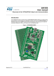
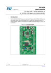
UM1525
User manual
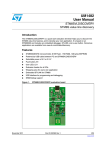
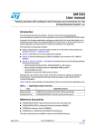
STM32F0DISCOVERY
Discovery kit for STM32 F0 microcontrollers
Introduction
The STM32F0DISCOVERY helps you to discover the STM32 F0 Cortex™-M0 features and
to develop your applications easily. It is based on STM32F051R8T6, an STM32 F0 series
32-bit ARM® Cortex™ microcontroller, and includes an ST-LINK/V2 embedded debug tool,
LEDs, push buttons and a prototyping board.
May 2012
Figure 1.
STM32F0DISCOVERY
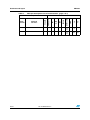
Table 1.
Applicable tools
Type
Part number
Evaluation tools
STM32F0DISCOVERY
Doc ID 022910 Rev 2
1/41
www.st.com
Contents
UM1525
Contents
1
Conventions . . . . . . . . . . . . . . . . . . . . . . . . . . . . . . . . . . . . . . . . . . . . . . . . 6
2
Quick start . . . . . . . . . . . . . . . . . . . . . . . . . . . . . . . . . . . . . . . . . . . . . . . . . 7
2.1
Getting started . . . . . . . . . . . . . . . . . . . . . . . . . . . . . . . . . . . . . . . . . . . . . . 7
2.2
System requirements . . . . . . . . . . . . . . . . . . . . . . . . . . . . . . . . . . . . . . . . . 7
2.3
Development toolchain supporting the STM32F0DISCOVERY . . . . . . . . . 7
2.4
Order code . . . . . . . . . . . . . . . . . . . . . . . . . . . . . . . . . . . . . . . . . . . . . . . . . 7
3
Features . . . . . . . . . . . . . . . . . . . . . . . . . . . . . . . . . . . . . . . . . . . . . . . . . . . 8
4
Hardware and layout . . . . . . . . . . . . . . . . . . . . . . . . . . . . . . . . . . . . . . . . . 9
5
4.1
STM32F051R8T6 microcontroller . . . . . . . . . . . . . . . . . . . . . . . . . . . . . . 12
4.2
Embedded ST-LINK/V2 . . . . . . . . . . . . . . . . . . . . . . . . . . . . . . . . . . . . . . 14
4.2.1
Using ST-LINK/V2 to program/debug the STM32 F0 on board . . . . . . . 15
4.2.2
Using ST-LINK/V2 to program/debug an external STM32 application . . 16
4.3
Power supply and power selection . . . . . . . . . . . . . . . . . . . . . . . . . . . . . . 17
4.4
LEDs . . . . . . . . . . . . . . . . . . . . . . . . . . . . . . . . . . . . . . . . . . . . . . . . . . . . 17
4.5
Push buttons . . . . . . . . . . . . . . . . . . . . . . . . . . . . . . . . . . . . . . . . . . . . . . 17
4.6
JP2 (Idd) . . . . . . . . . . . . . . . . . . . . . . . . . . . . . . . . . . . . . . . . . . . . . . . . . . 17
4.7
OSC clock . . . . . . . . . . . . . . . . . . . . . . . . . . . . . . . . . . . . . . . . . . . . . . . . 18
4.7.1
OSC clock supply . . . . . . . . . . . . . . . . . . . . . . . . . . . . . . . . . . . . . . . . . 18
4.7.2
OSC 32 KHz clock supply . . . . . . . . . . . . . . . . . . . . . . . . . . . . . . . . . . . 18
4.8
Solder bridges . . . . . . . . . . . . . . . . . . . . . . . . . . . . . . . . . . . . . . . . . . . . . 19
4.9
Extension connectors . . . . . . . . . . . . . . . . . . . . . . . . . . . . . . . . . . . . . . . . 20
Connecting modules on the prototyping board . . . . . . . . . . . . . . . . . . 27
5.1
Mikroelektronica accessory boards . . . . . . . . . . . . . . . . . . . . . . . . . . . . . 27
5.2
ST MEMS “adapter boards”, standard DIL24 socket . . . . . . . . . . . . . . . . 30
5.3
Arduino shield boards . . . . . . . . . . . . . . . . . . . . . . . . . . . . . . . . . . . . . . . . 33
6
Mechanical drawing . . . . . . . . . . . . . . . . . . . . . . . . . . . . . . . . . . . . . . . . 36
7
Electrical schematics . . . . . . . . . . . . . . . . . . . . . . . . . . . . . . . . . . . . . . . 37
2/41
Doc ID 022910 Rev 2
UM1525
8
Contents
Revision history . . . . . . . . . . . . . . . . . . . . . . . . . . . . . . . . . . . . . . . . . . . 40
Doc ID 022910 Rev 2
3/41
List of tables
UM1525
List of tables
Table 1.
Table 2.
Table 3.
Table 4.
Table 5.
Table 6.
Table 7.
Table 8.
Table 9.
Table 10.
Table 11.
Table 12.
4/41
Applicable tools. . . . . . . . . . . . . . . . . . . . . . . . . . . . . . . . . . . . . . . . . . . . . . . . . . . . . . . . . . . 1
ON/OFF conventions . . . . . . . . . . . . . . . . . . . . . . . . . . . . . . . . . . . . . . . . . . . . . . . . . . . . . . 6
Jumper states . . . . . . . . . . . . . . . . . . . . . . . . . . . . . . . . . . . . . . . . . . . . . . . . . . . . . . . . . . . 14
Debug connector CN3 (SWD) . . . . . . . . . . . . . . . . . . . . . . . . . . . . . . . . . . . . . . . . . . . . . . 16
Solder bridge settings . . . . . . . . . . . . . . . . . . . . . . . . . . . . . . . . . . . . . . . . . . . . . . . . . . . . . 19
MCU pin description versus board function . . . . . . . . . . . . . . . . . . . . . . . . . . . . . . . . . . . . 20
Connecting using mikroBUS™ . . . . . . . . . . . . . . . . . . . . . . . . . . . . . . . . . . . . . . . . . . . . . . 27
Connecting using IDC10 . . . . . . . . . . . . . . . . . . . . . . . . . . . . . . . . . . . . . . . . . . . . . . . . . . . 28
Connecting with a DIL24 board . . . . . . . . . . . . . . . . . . . . . . . . . . . . . . . . . . . . . . . . . . . . . 30
Supported MEMS adapter boards . . . . . . . . . . . . . . . . . . . . . . . . . . . . . . . . . . . . . . . . . . . 32
Connecting with Arduino shields. . . . . . . . . . . . . . . . . . . . . . . . . . . . . . . . . . . . . . . . . . . . . 33
Document revision history . . . . . . . . . . . . . . . . . . . . . . . . . . . . . . . . . . . . . . . . . . . . . . . . . 40
Doc ID 022910 Rev 2
UM1525
List of figures
List of figures
Figure 1.
Figure 2.
Figure 3.
Figure 4.
Figure 5.
Figure 6.
Figure 7.
Figure 8.
Figure 9.
Figure 10.
Figure 11.
Figure 12.
Figure 13.
Figure 14.
Figure 15.
Figure 16.
STM32F0DISCOVERY . . . . . . . . . . . . . . . . . . . . . . . . . . . . . . . . . . . . . . . . . . . . . . . . . . . . . 1
Hardware block diagram . . . . . . . . . . . . . . . . . . . . . . . . . . . . . . . . . . . . . . . . . . . . . . . . . . . 9
Top layout . . . . . . . . . . . . . . . . . . . . . . . . . . . . . . . . . . . . . . . . . . . . . . . . . . . . . . . . . . . . . 10
Bottom layout . . . . . . . . . . . . . . . . . . . . . . . . . . . . . . . . . . . . . . . . . . . . . . . . . . . . . . . . . . . 11
STM32F051R8T6 package. . . . . . . . . . . . . . . . . . . . . . . . . . . . . . . . . . . . . . . . . . . . . . . . . 12
STM32F051R8T6 block diagram . . . . . . . . . . . . . . . . . . . . . . . . . . . . . . . . . . . . . . . . . . . . 13
Typical configuration . . . . . . . . . . . . . . . . . . . . . . . . . . . . . . . . . . . . . . . . . . . . . . . . . . . . . 14
STM32F0DISCOVERY connections image . . . . . . . . . . . . . . . . . . . . . . . . . . . . . . . . . . . . 15
ST-LINK connections image . . . . . . . . . . . . . . . . . . . . . . . . . . . . . . . . . . . . . . . . . . . . . . . . 16
Using IDC10 and mikroBUS™ connectors . . . . . . . . . . . . . . . . . . . . . . . . . . . . . . . . . . . . . 29
DIL24 socket connections. . . . . . . . . . . . . . . . . . . . . . . . . . . . . . . . . . . . . . . . . . . . . . . . . . 31
Arduino shield board connections. . . . . . . . . . . . . . . . . . . . . . . . . . . . . . . . . . . . . . . . . . . . 35
STM32F0DISCOVERY mechanical drawing . . . . . . . . . . . . . . . . . . . . . . . . . . . . . . . . . . . 36
STM32F0DISCOVERY . . . . . . . . . . . . . . . . . . . . . . . . . . . . . . . . . . . . . . . . . . . . . . . . . . . . 37
ST-LINK/V2 (SWD only) . . . . . . . . . . . . . . . . . . . . . . . . . . . . . . . . . . . . . . . . . . . . . . . . . . . 38
MCU . . . . . . . . . . . . . . . . . . . . . . . . . . . . . . . . . . . . . . . . . . . . . . . . . . . . . . . . . . . . . . . . . . 39
Doc ID 022910 Rev 2
5/41
Conventions
1
UM1525
Conventions
Table 2 provides the definition of some conventions used in the present document.
Table 2.
ON/OFF conventions
Convention
Definition
Jumper JP1 ON
Jumper fitted
Jumper JP1 OFF
Jumper not fitted
Solder bridge SBx ON
SBx connections closed by solder
Solder bridge SBx OFF SBx connections left open
6/41
Doc ID 022910 Rev 2
UM1525
2
Quick start
Quick start
The STM32F0DISCOVERY is a low-cost and easy-to-use development kit to quickly
evaluate and start development with an STM32 F0 series microcontroller.
Before installing and using the product, please accept the Evaluation Product License
Agreement from www.st.com/stm32f0discovery.
For more information on the STM32F0DISCOVERY and for demonstration software, visit
www.st.com/stm32f0discovery.
2.1
Getting started
Follow the sequence below to configure the STM32F0DISCOVERY board and launch the
DISCOVER application:
2.2
2.3
2.4
1.
Check jumper position on the board, JP2 on, CN2 on (Discovery selected).
2.
Connect the STM32F0DISCOVERY board to a PC with a USB cable ‘type A to mini-B’
through USB connector CN1 to power the board. Red LED LD1 (PWR) and LD2 (COM)
light up and green LED LD3 blinks.
3.
Press user button B1 (bottom left corner of the board).
4.
Observe how the green LED LD3 blinking changes according to USER button B1
clicks.
5.
Each click on USER button B1 is confirmed by the blue LED LD4.
6.
To study or modify the DISCOVER project related to this demo, visit
www.st.com/stm32f0discovery and follow the tutorial.
7.
Discover the STM32F0 features, download and execute programs proposed in the list
of projects.
8.
Develop your own application using available examples.
System requirements
●
Windows PC (XP, Vista, 7)
●
USB type A to Mini-B USB cable
Development toolchain supporting the STM32F0DISCOVERY
●
Altium®, TASKING™ VX-toolset
●
ARM®, Atollic TrueSTUDIO®
●
IAR™, EWARM (IAR Embedded Workbench®)
●
Keil™, MDK-ARM™
Order code
To order the STM32F0 Discovery kit, use the order code STM32F0DISCOVERY.
Doc ID 022910 Rev 2
7/41
Features
3
UM1525
Features
The STM32F0DISCOVERY kit offers the following features:
8/41
●
STM32F051R8T6 microcontroller featuring 64 KB Flash, 8 KB RAM in an LQFP64
package
●
On-board ST-LINK/V2 with selection mode switch to use the kit as a standalone
ST-LINK/V2 (with SWD connector for programming and debugging)
●
Board power supply: through USB bus or from an external 5 V supply voltage
●
External application power supply: 3 V and 5 V
●
Four LEDs:
–
LD1 (red) for 3.3 V power on
–
LD2 (red/green) for USB communication
–
LD3 (green) for PC9 output
–
LD4 (blue) for PC8 output
●
Two push buttons (user and reset)
●
Extension header for LQFP64 I/Os for quick connection to prototyping board and easy
probing.
●
An additional board is provided with the kit which can be connected to the extension
connector for even easier prototyping and probing.
●
A large number of free ready-to-run application firmware examples are available on
www.st.com/stm32f0discovery to support quick evaluation and development.
Doc ID 022910 Rev 2
UM1525
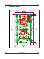
Hardware and layout
The STM32F0DISCOVERY is designed around the STM32F051R8T6 microcontroller in a
64-pin LQFP package.
Figure 2 illustrates the connections between the STM32F051R8T6 and its peripherals (STLINK/V2, push button, LEDs and connectors).
Figure 3 and Figure 4 help you to locate these features on the STM32F0DISCOVERY.
Hardware block diagram
-INI
53"
%MBEDDED
34,).+6
37$
34-&24
)/
)/
)/
2%3%4
,%$
,$0#
"
234
,%$
,$0#
"
53%2
(EADER
Figure 2.
(EADER
4
Hardware and layout
-36
Doc ID 022910 Rev 2
9/41
Hardware and layout
Figure 3.
UM1525
Top layout
(red/green LED) LD2
COM
LD1 (red LED)
PWR
ST-LINK/V2
5V power supply
input output
3V power supply
input output
CN3
SWD connector
CN2
ST-LINK/DISCOVERY
selector
JP2
IDD measurement
SB1 (VBAT)
SB3 (B1-USER)
B2 reset button
STM32F051R8T6
SB4 (B2-RESET)
B1 user button
(green LED) LD3
LD4 (blue LED)
MS30024V1
Note:
10/41
Pin 1 of CN2, CN3, P1 and P2 connectors are identified by a square.
Doc ID 022910 Rev 2
UM1525
Figure 4.
Hardware and layout
Bottom layout
SB5, SB7, SB9, SB11
(RESERVED)
SB6, SB8, SB10, SB12
(DEFAULT)
SB13 (STM_RST)
SB14, SB15 (RX, TX)
SB16, SB17 (X2 crystal)
SB18 (MCO)
SB19 (NRST)
SB20, SB21 (X3 crystal)
SB22 (T_SWO)
MS30025V1
Doc ID 022910 Rev 2
11/41
Hardware and layout
4.1
UM1525
STM32F051R8T6 microcontroller
This 32-bit low- and medium-density advanced ARM™ MCU with a high-performance ARM
Cortex™-M0 32-bit RISC core has 64 Kbytes Flash, 8 Kbytes RAM, RTC, timers, ADC,
DAC, comparators and communication interfaces.
Figure 5.
STM32F051R8T6 package
34-&24
+BYTEOF&LASHMEMORY
+BYTESOF2!-
,1&0XMM
-36
The STM32 F0 delivers 32-bit performance and STM32 DNA essentials into applications
typically addressed by 8- or 16-bit microcontrollers. It benefits from the combination of realtime performance, low-power operation, advanced architecture and peripherals associated
to the STM32 ecosystem, which has made the STM32 a reference in the market. Now all
this is accessible for cost-sensitive applications. The STM32 F0 offers unparalleled flexibility
and scalability for home entertainment products, appliances, and industrial equipment.
This device provides the following benefits.
●
Superior code execution for better performance and excellent code efficiency for
reduced embedded memory usage
●
High-performance connectivity and advanced analog peripherals to support a wide
range of applications
●
Flexible clock options and low power modes with fast wake-up for low power
consumption
It has the following key features:
●
●
Core and operating conditions
–
ARM® Cortex™-M0 0.9 DMIPS/MHz up to 48 MHz
–
1.8/2.0 to 3.6 V supply range
High-performance connectivity
–
●
12/41
6 Mbit/s USART
–
18 Mbit/s SPI with 4- to 16-bit data frame
–
1 Mbit/s I²C fast-mode plus
–
HDMI CEC
Enhanced control
–
1x 16-bit 3-phase PWM motor control timer
–
5x 16-bit PWM timers
–
1x 16-bit basic timer
–
1x 32-bit PWM timer
–
12 MHz I/O toggling
Doc ID 022910 Rev 2
UM1525
3ERIAL7IRE
$EBUG
6$$
FLASH OBL
)NTERFACE
37#,+
37$!4
AS!&
STM32F051R8T6 block diagram
.6)#
'0$-!
CHANNELS
"US-ATRIX
.6)#
32!-
#/24%8-#05
F(#,+-(Z
CONTROLLER
Figure 6.
Hardware and layout
0/7%2
6/,4 2%'
64/ 6
&,!3(
+"
BITS
6$$ TO 6
633
6$$
0/2
2ESET
32! +"
6$$!
)NT
3500,9
350%26)3)/.
0/2 0$2
6
$$
06$
2#(3-(Z
2#(3-(Z
.234
6$$!
6$$!
6$$
2#,3
84!, /3#
-(Z
0,,
/3#). 0&
/3#/54 0&
)77$'
0!;=
'0)/PORT!
0";=
'0)/PORT"
0#;=
'0)/PORT#
0$
'0)/PORT$
0&;=
'0)/PORT&
GROUPS OF
CHANNELS
!(" DECODER
2%3%4
#,/#+
#/.42/,
!("0#,+
!0"0#,+
!$##,+
#%##,+
53!24#,+
(#,+
&#,+
#2#
#ONTROLLER
-/3)3$
-)3/-#+
3#+#+
.3373AS!&
-/3) -)3/
3#+ .33
AS !&
84!, K(Z
"ACKUP
REG
%84)4
7+50
77$'
4!-0%224#
!,!2- /54
24# INTERFACE
4)-%2
CHANNELS
COMPL CHANNELS
"2+ %42 INPUT AS !&
4)-%2
CH %42 AS !&
4)-%2
CH %42 AS !&
4)-%2
CHANNEL AS !&
4)-%2
CHANNELS
COMPL "2+ AS !&
4)-%2
CHANNEL
COMPL "2+ AS !&
4)-%2
CHANNEL
COMPL "2+ AS !&
53!24
2848 #43 243
#+ AS !&
53!24
2848 #43 243
#+ AS !&
)2?/54AS!&
30))3
$"'-#5
30)
393#&' )&
3#,3$!3-"AL
M! FOR &-
AS !&
)#
)#
).054
).054
/54054
AS!&
/3#?).
/3#?/54
!("
!0"
!&
6"!4 6 TO 6
637
24#
!NALOG
SWITCHES 4OUCH 3ENSING
39.#
0OWER
#ONTROLLER
3#,3$!
AS !&
'0 #OMPARATOR '0 #OMPARATOR 6$$!
($-)#%#
#%# AS !&
4EMP SENSOR
!$INPUTS
BIT!$# )&
4)-%2 )& BIT$!#
)&
$!#?/54 AS !&
6$$!
633!
6$$!
6$$!
-36
Doc ID 022910 Rev 2
13/41
Hardware and layout
4.2
UM1525
Embedded ST-LINK/V2
The ST-LINK/V2 programming and debugging tool is integrated on the
STM32F0DISCOVERY. The embedded ST-LINK/V2 can be used in 2 different ways
according to the jumper states (see Table 3):
●
Program/debug the MCU on board,
●
Program/debug an MCU in an external application board using a cable connected to
SWD connector CN3.
The embedded ST-LINK/V2 supports only SWD for STM32 devices. For information about
debugging and programming features refer to user manual UM1075 (ST-LINK/V2 in-circuit
debugger/programmer for STM8 and STM32) which describes in detail all the ST-LINK/V2
features.
Figure 7.
Typical configuration
(ARDWAREREQUIREMENTS
53"CABLETYPE!TOMINI"
COMPUTERWITH7INDOWS806ISTAOR
$EVELOPMENTTOOLCHAIN
!LTIUM4!3+).'684OOLSET
!TOLLIC4RUE345$)/
)!2%7!2+EIL-$+!2-
-36
Table 3.
Jumper states
Jumper state
14/41
Description
Both CN2 jumpers ON
ST-LINK/V2 functions enabled for on board programming (default)
Both CN2 jumpers OFF
ST-LINK/V2 functions enabled for application through external CN3
connector (SWD supported)
Doc ID 022910 Rev 2
UM1525
4.2.1
Hardware and layout
Using ST-LINK/V2 to program/debug the STM32 F0 on board
To program the STM32 F0 on board, simply plug in the two jumpers on CN2, as shown in
Figure 8 in red, but do not use the CN3 connector as that could disturb communication with
the STM32F051R8T6 of the STM32F0DISCOVERY.
Figure 8.
STM32F0DISCOVERY connections image
Doc ID 022910 Rev 2
15/41
Hardware and layout
4.2.2
UM1525
Using ST-LINK/V2 to program/debug an external STM32 application
It is very easy to use the ST-LINK/V2 to program the STM32 on an external application.
Simply remove the 2 jumpers from CN2 as shown in Figure 9, and connect your application
to the CN3 debug connector according to Table 4.
Note:
SB19 and SB22 must be OFF if you use CN3 pin 5 in your external application.
Table 4.
Figure 9.
16/41
Debug connector CN3 (SWD)
Pin
CN3
Designation
1
VDD_TARGET
VDD from application
2
SWCLK
SWD clock
3
GND
Ground
4
SWDIO
SWD data input/output
5
NRST
RESET of target MCU
6
SWO
Reserved
ST-LINK connections image
Doc ID 022910 Rev 2
UM1525
4.3
Hardware and layout
Power supply and power selection
The power supply is provided either by the host PC through the USB cable, or by an external
5V power supply.
The D1 and D2 diodes protect the 5V and 3V pins from external power supplies:
4.4
4.5
4.6
●
5V and 3V can be used as output power supplies when another application board is
connected to pins P1 and P2.
In this case, the 5V and 3V pins deliver a 5V or 3V power supply and power
consumption must be lower than 100 mA.
●
5V can also be used as input power supplies e.g. when the USB connector is not
connected to the PC.
In this case, the STM32F0DISCOVERY board must be powered by a power supply unit
or by auxiliary equipment complying with standard EN-60950-1: 2006+A11/2009, and
must be Safety Extra Low Voltage (SELV) with limited power capability.
LEDs
●
LD1 PWR: Red LED indicates that the board is powered.
●
LD2 COM: Tricolor LED (COM) advises on the communication status as follows:
–
Slow blinking Red LED/Off: At power on before USB initialization
–
Fast blinking Red LED/Off: After the first correct communication between PC and
STLINK/V2 (enumeration)
–
Red LED On: When initialization between PC and ST-LINK/V2 is successfully
finished
–
Green LED On: After successful target communication initialization
–
Blinking Red/Green LED: During communication with target
–
Red LED On: Communication finished and OK
–
Orange LED On: Communication failure
●
User LD3: Green user LED connected to the I/O PC9 of the STM32F051R8T6.
●
User LD4: Blue user LED connected to the I/O PC8 of the STM32F051R8T6.
Push buttons
●
B1 USER: User push button connected to the I/O PA0 of the STM32F051R8T6.
●
B2 RESET: Push button used to RESET the STM32F051R8T6.
JP2 (Idd)
Jumper JP2, labeled Idd, allows the consumption of STM32F051R8T6 to be measured by
removing the jumper and connecting an ammeter.
●
Jumper on: STM32F051R8T6 is powered (default).
●
Jumper off: an ammeter must be connected to measure the STM32F051R8T6 current,
(if there is no ammeter, the STM32F051R8T6 is not powered).
Doc ID 022910 Rev 2
17/41
Hardware and layout
UM1525
4.7
OSC clock
4.7.1
OSC clock supply
PF0 and PF1 can be used as GPIO or as HSE oscillator. By default these I/Os are
configured as GPIO, so SB16 and SB17 are closed, SB18 is open and R22, R23, C13 and
C14 are not populated.
An external HSE clock can be provided to the MCU in three ways:
●
●
●
4.7.2
MCO from ST-LINK. From MCO of the STM32F103. This frequency cannot be
changed, it is fixed at 8 MHz and connected to PF0-OSC_IN of the STM32F051R8T6.
Configuration needed:
–
SB16, SB18 CLOSED
–
R22, R23 removed
–
SB17 OPEN
Oscillator onboard. From X2 crystal (not provided). For typical frequencies and its
capacitors and resistors, please refer to the STM32F051R8T6 Datasheet.
Configuration needed:
–
SB16, SB17 SB18 OPEN
–
R22, R23, C13, C14 soldered
Oscillator from external PF0. From external oscillator through pin 7 of the P1
connector. Configuration needed:
–
SB16, SB17 CLOSED
–
SB18 OPEN
–
R22 and R23 removed
OSC 32 KHz clock supply
PC14 and PC15 can be used as GPIO or as LSE oscillator. By default these I/Os are
configured as GPIO, so SB20 & SB21 are closed and X3, R24, R25 are not populated.
An external LSE clock can be provided to the MCU in two ways:
●
●
18/41
Oscillator onboard. From X3 crystal (not provided). Configuration needed:
–
SB20, SB21 OPEN
–
C15, C16, R24 and R25 soldered.
Oscillator from external PC14. From external oscillator trough the pin 5 of P1
connector. Configuration needed:
–
SB20, SB21 CLOSED
–
R24 and R25 removed
Doc ID 022910 Rev 2
UM1525
Hardware and layout
4.8
Solder bridges
Table 5.
Solder bridge settings
Bridge
State(1)
Description
SB16,17
(X2 crystal)(2)
OFF
X2, C13, C14, R22 and R23 provide a clock. PF0, PF1 are disconnected
from P1.
ON
PF0, PF1 are connected to P1 (R22, R23 and SB18 must not be fitted).
SB6,8,10,12 (Default)
ON
Reserved, do not modify.
SB5,7,9,11 (Reserved)
OFF
Reserved, do not modify.
SB20,21
(X3 crystal)
OFF
X3, C15, C16, R24 and R25 deliver a 32 KHz clock. PC14, PC15 are not
connected to P1.
ON
PC14, PC15 are only connected to P1 (R24, R25 must not be fitted).
ON
B2 push button is connected to the NRST pin of the STM32F051R8T6
MCU.
OFF
B2 push button is not connected the NRST pin of the STM32F051R8T6
MCU.
SB3
(B1-USER)
ON
B1 push button is connected to PA0.
OFF
B1 push button is not connected to PA0.
SB1
(VBAT powered from VDD)
ON
VBAT is permanently powered from VDD.
OFF
VBAT is not powered from VDD but pin3 of P1.
SB14,15
(RX,TX)
OFF
Reserved, do not modify.
ON
Reserved, do not modify.
ON
NRST signal of the CN3 connector is connected to the NRST pin of the
STM32F051R8T6 MCU.
OFF
NRST signal of the CN3 connector is not connected to the NRST pin of the
STM32F051R8T6 MCU.
ON
SWO signal of the CN3 connector is connected to PB3.
OFF
SWO signal is not connected.
OFF
No incidence on STM32F103C8T6 (ST-LINK/V2) NRST signal.
ON
STM32F103C8T6 (ST-LINK/V2) NRST signal is connected to GND.
ON
BOOT0 signal of the STM32F051R8T6 MCU is held low through a
510 Ohm pull-down resistor.
OFF
BOOT0 signal of the STM32F051R8T6 MCU can be set high through a
10 KOhm pull-up resistor R27 to solder.
ON
Provides the 8 MHz for OSC_IN from MCO of STM32F103C8T6.
OFF
See SB16, SB17 description.
SB4
(B2-RESET)
SB19
(NRST)
SB22
(T_SWO)
SB13
(STM_RST)
SB2
(BOOT0)
SB18
(MCO)(2)
1. Default SBx state is shown in bold.
2. OSC_IN clock comes from MCO if SB18 is ON and SB16,17 are OFF
and comes from X2 if SB18 is OFF and SB16,17 are ON.
Doc ID 022910 Rev 2
19/41
Hardware and layout
4.9
UM1525
Extension connectors
The male headers P1 and P2 can connect the STM32F0DISCOVERY to a standard
prototyping/wrapping board. STM32F051R8T6 GPI/Os are available on these connectors.
P1 and P2 can also be probed by an oscilloscope, logical analyzer or voltmeter.
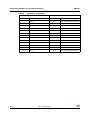
Table 6.
MCU pin description versus board function (page 1 of 7)
MCU pin
BOOT0
60
NRST
NRST
7
RESET
PA0
2_CTS,
IN0,
2_CH1_ETR,
1_INM6,
1_OUT,
TSC_G1_IO1,
RTC_TAMP2,
WKUP1
14
USER
6
PA1
2_RTS,
IN1,
2_CH2,
1_INP,
TSC_G1_IO2,
EVENTOUT
15
16
PA2
2_TX,
IN2,
2_CH3,
15_CH1,
2_INM6,
2_OUT,
TSC_G1_IO3
16
17
PA3
2_RX,
IN3,
2_CH4,
15_CH2,
2_INP,
TSC_G1_IO4,
17
18
Doc ID 022910 Rev 2
NRST
BOOT0
P2
P1
CN3
Power supply
Free I/O
OSC
SWD
LED
Push button
20/41
Alternate
functions
LQFP64
Main
function
Board function
5
10
15
UM1525
Hardware and layout
Table 6.
MCU pin description versus board function (page 2 of 7)
MCU pin
P2
P1
CN3
Power supply
Free I/O
OSC
SWD
LED
Push button
Alternate
functions
LQFP64
Main
function
Board function
PA4
1_NSS / 1_WS,
2_CK,
IN4,
14_CH1,
DAC1_OUT,
1_INM4,
2_INM4,
TSC_G2_IO1
20
21
PA5
1_SCK / 1_CK,
CEC,
IN5,
2_CH1_ETR,
(DAC2_OUT),
1_INM5,
2_INM5,
TSC_G2_IO2
21
22
PA6
1_MISO / 1_MCK,
IN6,
3_CH1,
1_BKIN,
16_CH1,
1_OUT,
TSC_G2_IO3,
EVENTOUT
22
23
PA7
1_MOSI / 1_SD,
IN7,
3_CH2,
14_CH1,
1_CH1N,
17_CH1,
2_OUT,
TSC_G2_IO4,
EVENTOUT
23
24
PA8
1_CK,
1_CH1,
EVENTOUT,
MCO
41
25
PA9
1_TX,
1_CH2,
15_BKIN,
TSC_G4_IO1
42
24
Doc ID 022910 Rev 2
21/41
Hardware and layout
Table 6.
UM1525
MCU pin description versus board function (page 3 of 7)
MCU pin
P2
P1
CN3
Power supply
Free I/O
OSC
SWD
LED
Push button
PA10
1_RX,
1_CH3,
17_BKIN,
TSC_G4_IO2
43
23
PA11
1_CTS,
1_CH4,
1_OUT,
TSC_G4_IO3,
EVENTOUT
44
22
PA12
1_RTS,
1_ETR,
2_OUT,
TSC_G4_IO4,
EVENTOUT
45
21
PA13
IR_OUT,
SWDAT
46
PA14
2_TX,
SWCLK
49
PA15
1_NSS / 1_WS,
2_RX,
2_CH1_ETR,
EVENTOUT
50
PB0
IN8,
3_CH3,
1_CH2N,
TSC_G3_IO2,
EVENTOUT
26
27
PB1
IN9,
3_CH4,
14_CH1,
1_CH3N,
TSC_G3_IO3
27
28
PB2 or
NPOR
(1.8V
mode)
TSC_G3_IO4
28
29
PB3
1_SCK / 1_CK,
2_CH2,
TSC_G5_IO1,
EVENTOUT
55
4
20
2
17
16
SWO
Doc ID 022910 Rev 2
SWDIO SWCLK
22/41
Alternate
functions
LQFP64
Main
function
Board function
6
11
UM1525
Hardware and layout
Table 6.
MCU pin description versus board function (page 4 of 7)
MCU pin
P2
P1
CN3
Power supply
Free I/O
OSC
SWD
LED
Push button
Alternate
functions
LQFP64
Main
function
Board function
PB4
1_MISO / 1_MCK,
3_CH1,
TSC_G5_IO2,
EVENTOUT
56
10
PB5
1_MOSI / 1_SD,
1_SMBA,
16_BKIN,
3_CH2
57
9
PB6
1_SCL,
1_TX,
16_CH1N,
TSC_G5_IO3
58
8
PB7
1_SDA,
1_RX,
17_CH1N,
TSC_G5_IO4
59
7
PB8
1_SCL,
CEC,
16_CH1,
TSC_SYNC
61
4
PB9
1_SDA,
IR_EVENTOUT,
17_CH1,
EVENTOUT
62
3
PB10
2_SCL,
CEC,
2_CH3,
SYNC
29
30
PB11
2_SDA,
2_CH4,
G6_IO1,
EVENTOUT
30
31
PB12
2_NSS,
1_BKIN,
G6_IO2,
EVENTOUT
33
32
PB13
2_SCK,
1_CH1N,
G6_IO3
34
32
Doc ID 022910 Rev 2
23/41
Hardware and layout
Table 6.
UM1525
MCU pin description versus board function (page 5 of 7)
MCU pin
P2
P1
CN3
Power supply
Free I/O
OSC
SWD
LED
Push button
35
31
PB15
2_MOSI,
1_CH3N,
15_CH1N,
15_CH2,
RTC_REFIN
36
30
PC0
IN10,
EVENTOUT
8
11
PC1
IN11,
EVENTOUT
9
12
PC2
IN12,
EVENTOUT
10
13
PC3
IN13,
EVENTOUT
11
14
PC4
IN14,
EVENTOUT
24
25
PC5
IN15,
TSC_G3_IO1
25
26
PC6
3_CH1
37
29
PC7
3_CH2
38
28
PC8
3_CH3
39
PC9
3_CH4
40
BLUE GREEN
PB14
2_MISO,
1_CH2N,
15_CH1,
G6_IO4
27
26
PC10
51
15
PC11
52
14
PC12
53
13
PC13
24/41
Alternate
functions
LQFP64
Main
function
Board function
RTC_TAMP1,
RTC_TS,
RTC_OUT,
WKUP2
2
Doc ID 022910 Rev 2
4
UM1525
Hardware and layout
Table 6.
MCU pin description versus board function (page 6 of 7)
MCU pin
P2
P1
CN3
Power supply
Free I/O
OSC
SWD
LED
Push button
Alternate
functions
LQFP64
Main
function
Board function
OSC32_IN OSC32_OUT
PC14OSC32_ OSC32_IN
IN
3
PC15OSC32_ OSC32_OUT
OUT
4
PD2
3_ETR
54
PF0OSC_IN
OSC_IN
5
PF1OSC_
OUT
OSC_OUT
6
PF4
EVENTOUT
18
19
PF5
EVENTOUT
19
20
PF6
2_SCL
47
19
PF7
2_SDA
48
18
VBAT
VBAT
1
64
VDD_2
32
VDDA
13
VSS_1
63
VSS_2
31
VSSA
12
6
12
OSC_IN OSC_OUT
VDD_1
5
7
8
3
5V
1
3V
VDD GND GND
GND
Doc ID 022910 Rev 2
1
5
2
2
3
25/41
Hardware and layout
Table 6.
UM1525
MCU pin description versus board function (page 7 of 7)
MCU pin
P2
P1
CN3
Power supply GND GND
Free I/O
OSC
SWD
Doc ID 022910 Rev 2
LED
Push button
26/41
Alternate
functions
LQFP64
Main
function
Board function
9
33
33
UM1525
5
Connecting modules on the prototyping board
Connecting modules on the prototyping board
This section gives some examples of how to connect ready-to-use modules available from
different manufacturers to the STM32F0DISCOVERY kit via the prototyping board included
in the kit.
Software examples, based on the connections described below, are available at
www.st.com/stm32f0discovery.
5.1
Mikroelektronica accessory boards
Mikroelektronika, http://www.mikroe.com, has specified two standard connectors for their
accessory boards, named mikroBUS™ (http://www.mikroe.com/mikrobus_specs.pdf) and
IDC10.
MikroBUS™ is a 16-pin connector to connect accessory boards very quickly and easily to a
microcontroller board through SPI, USART or I2C communications, along with additional
pins such as Analog Input, PWM and Interrupt.
The set of mikroElektronika boards compatible with mikroBUS™ is called “Click boards”.
IDC10 is a 10-pin connector to connect the general purpose I/O of an MCU to other
accessory boards.
The tables below are one solution for connecting mikroBUS™ and IDC boards to the
STM32F0DISCOVERY; this solution used in the different examples is available at
www.st.com/stm32f0discovery.
Table 7.
Connecting using mikroBUS™
Mikroelektronica mikroBUS™
STM32F0DISCOVERY
Pin
Description
Pin
Description
AN
Analog pin
PA4
DAC1_OUT
RST
Reset pin
PB13
GPIO OUTPUT (5V tolerant)
SPI Chip Select line
PA11
GPIO OUTPUT (5V tolerant)
SCK
SPI Clock line
PB3
SPI1_SCK
MISO
SPI Slave Output line
PB4
SPI1_MISO
MOSI
SPI Slave Input line
PB5
SPI1_MOSI
PWM
PWM output line
PA8
TIM1_CH1
CS
INT
Hardware Interrupt line
RX
UART Receive line
PA3
USART2_RX
TX
UART Transmit line
PA2
USART2_TX
SCL
I2C Clock line
PF6
I2C2_SCL
SDA
I2C Data line
PF7
I2C2_SDA
5V
Power line
5V
VCC 5V power line
Doc ID 022910 Rev 2
PB12
GPIO INPUT EXTI (5V tolerant)
27/41
Connecting modules on the prototyping board
Table 8.
UM1525
Connecting using IDC10
Mikroelektronica IDC10 connector
28/41
STM32F0DISCOVERY
P0
GPIO
PC0
GPIO OUTPUT (3.3V tolerant)
P1
GPIO
PC1
GPIO OUTPUT (3.3V tolerant)
P2
GPIO
PC2
GPIO OUTPUT (3.3V tolerant)
P3
GPIO
PC3
GPIO OUTPUT (3.3V tolerant)
P4
GPIO
PC4
GPIO OUTPUT (3.3V tolerant)
P5
GPIO
PC5
GPIO OUTPUT (3.3V tolerant)
P6
GPIO
PC6
GPIO OUTPUT (5V tolerant)
P7
GPIO
PC7
GPIO OUTPUT (5V tolerant)
VCC
VCC 5V power line
3V
VDD
GND
Reference Ground
GND
VSS
P0
GPIO
PC0
GPIO OUTPUT (3.3V tolerant)
P1
GPIO
PC1
GPIO OUTPUT (3.3V tolerant)
P2
GPIO
PC2
GPIO OUTPUT (3.3V tolerant)
P3
GPIO
PC3
GPIO OUTPUT (3.3V tolerant)
Doc ID 022910 Rev 2
UM1525
Connecting modules on the prototyping board
The Figure 10 illustrates the connections between the STM32F0 Discovery and the 2
connectors, IDC10 and mikroBUS™.
Figure 10. Using IDC10 and mikroBUS™ connectors
Doc ID 022910 Rev 2
29/41
Connecting modules on the prototyping board
5.2
UM1525
ST MEMS “adapter boards”, standard DIL24 socket
STMicroelectronics has defined a standard DIL24 connector to easily evaluate its MEMS
sensors connected to a microcontroller through SPI or I2C communications.
Table 9 is one solution for connecting the DIL24 boards to the STM32F0DISCOVERY, this
solution is used in different examples and available at www.st.com/stm32f0discovery.
Table 9.
Connecting with a DIL24 board
ST MEMS DIL24 Eval board
STM32F0DISCOVERY
P01 VDD Power supply
3V
VDD
P02 Vdd_IO Power supply for I/O pins
3V
VDD
P13 GND 0V supply
GND
GND
P14 INT1 Inertial interrupt 1
PB12
GPIO INPUT EXTI (5V tolerant)
P15 INT2 inertial interrupt 2
PB11
GPIO INPUT EXTI (5V tolerant)
PA11
GPIO OUTPUT (5V tolerant)
P03 NC
P04 NC
P05 NC
P06 NC
P07 NC
P08 NC
P09 NC
P10 NC
P11 NC
P12 NC
P16 NC
P17 NC
P18 NC
P19 CS - 0:SPI enabled 1:I2C mode
P20
SCL (I2C serial clock)
SPC (SPI serial clock)
PB6
PB3
I2C1_SCL
SPI1_SCK
P21
SDA I2C Serial Data
SDI SPI Serial Data Input
PB7
PB5
I2C1_SDA
SPI1_MOSI
P22
SDO SPI Serial Data Output
I2C less significant bit of the device address
PB4
SPI1_MISO
P23 NC
P24 NC
30/41
Doc ID 022910 Rev 2
UM1525
Connecting modules on the prototyping board
Figure 11 illustrates the connections between the STM32F0 Discovery and the DIL24
socket.
Figure 11. DIL24 socket connections
Doc ID 022910 Rev 2
31/41
Connecting modules on the prototyping board
UM1525
Supported MEMS adapter boards
Table 10 is a list of supported MEMS adapter boards as of April, 2012.
Table 10.
Supported MEMS adapter boards
ST MEMS DIL24 Eval Board
Note:
32/41
Core product
STEVAL-MKI009V1
LIS3LV02DL
STEVAL-MKI013V1
LIS302DL
STEVAL-MKI015V1
LIS344ALH
STEVAL-MKI082V1
LPY4150AL
STEVAL-MKI083V1
LPY450AL
STEVAL-MKI084V1
LPY430AL
STEVAL-MKI085V1
LPY410AL
STEVAL-MKI086V1
LPY403AL
STEVAL-MKI087V1
LIS331DL
STEVAL-MKI088V1
LIS33DE
STEVAL-MKI089V1
LIS331DLH
STEVAL-MKI090V1
LIS331DLF
STEVAL-MKI091V1
LIS331DLM
STEVAL-MKI092V1
LIS331HH
STEVAL-MKI095V1
LPR4150AL
STEVAL-MKI096V1
LPR450AL
STEVAL-MKI097V1
LPR430AL
STEVAL-MKI098V1
LPR410AL
STEVAL-MKI099V1
LPR403AL
STEVAL-MKI105V1
LIS3DH
STEVAL-MKI106V1
LSM303DLHC
STEVAL-MKI107V1
L3G4200D
STEVAL-MKI107V2
L3GD20
STEVAL-MKI108V1
9AXISMODULE v1 [LSM303DLHC + L3G4200D]
STEVAL-MKI108V2
9AXISMODULE v2 [LSM303DLHC + L3GD20]
STEVAL-MKI110V1
AIS328DQ
STEVAL-MKI113V1
LSM303DLM
STEVAL-MKI114V1
MAG PROBE (based on LSM303DLHC)
STEVAL-MKI120V1
LPS331AP
STEVAL-MKI122V1
LSM330DLC
STEVAL-MKI123V1
LSM330D
STEVAL-MKI124V1
10AXISMODULE [LSM303DLHC + L3GD20+
LPS331AP]
STEVAL-MKI125V1
A3G4250D
For an up-to-date list, visit http://www.st.com/internet/evalboard/subclass/1116.jsp. The
DIL24 boards are described as “adapter boards” in the field “General Description”.
Doc ID 022910 Rev 2
UM1525
5.3
Connecting modules on the prototyping board
Arduino shield boards
Arduino™ is an open-source electronics prototyping platform based on flexible, easy-to-use
hardware and software. See http://www.arduino.cc for more information.
Arduino accessory boards are called “Shields” and can be easily connected to the
STM32F0 Discovery according to the following table.
Table 11.
Connecting with Arduino shields
Connecting with Arduino shields
Arduino power connector
Reset
STM32F0DISCOVERY
Reset from Shield board
3V3
VCC 3.3V power line
NRST
Reset discovery
3V
VDD
VDD
5V
VCC 5V power line
5V
GND
Reference Ground
GND
Reference Ground
GND
Reference Ground
GND
Reference Ground
External alimentation
VBAT
Jumper to fit
Vin
Arduino analog in connector
STM32F0DISCOVERY
A0
Analog input or Digital pin 14
PC0
ADC_IN10
A1
Analog input or Digital pin 15
PC1
ADC_IN11
A2
Analog input or Digital pin 16
PC2
ADC_IN12
A3
Analog input or Digital pin 17
PC3
ADC_IN13
A4
Analog input or SDA or Digital
pin 18
PC4 or PF7
ADC_IN14 or I2C2_SDA
A5
Analog input or SCL or Digital
pin 19
PC5 or PF6
ADC_IN15 or I2C2_SCL
Arduino digital connector
STM32F0DISCOVERY
D0
Digital pin 0 or RX
PA3
USART2_RX
D1
Digital pin 1 or TX
PA2
USART2_TX
D2
Digital pin 2 / External interrupt
PB12
EXTI (5V tolerant)
D3
Digital pin 3 / Ext int or PWM
PB11
EXTI (5V tolerant) or TIM2_CH4
D4
Digital pin 4
PA7
GPIO (3V tolerant)
D5
Digital pin 5 or PWM
PB9
TIM17_CH1
D6
Digital pin 6 or PWM
PB8
TIM16_CH1
D7
Digital pin 7
PA6
GPIO (3V tolerant)
D8
Digital pin 8
PA5
GPIO (3V tolerant)
D9
Digital pin 9 or PWM
PA4
TIM14_CH1
D10
Digital pin 10 or CS or PWM
PA11
TIM1_CH4
D11
Digital pin 11 or MOSI or PWM
PB5
SPI1_MOSI or TIM3_CH2
D12
Digital pin 12 or MISO
PB4
SPI1_MISO
D13
Digital pin 13 or SCK
PB3
SPI1_SCK
GND
Reference Ground
GND
Reference Ground
AREF
ADC voltage reference
Doc ID 022910 Rev 2
NC
Not connected
33/41
Connecting modules on the prototyping board
UM1525
Connecting with Arduino shields (continued)
Arduino ICSP connector
34/41
1
MISO
2
VCC 3.3V
3
SCK
4
5
6
STM32F0DISCOVERY
PB4
3V
SPI1_MISO
VDD
PB3
SPI1_SCK
MOSI
PB5
SPI1_MOSI
RST
NRST
Reset discovery
GND
GND
Reference Ground
Doc ID 022910 Rev 2
UM1525
Connecting modules on the prototyping board
Figure 12 illustrates the connections between the STM32F0 Discovery and the Arduino
shield boards.
Figure 12. Arduino shield board connections
Doc ID 022910 Rev 2
35/41
Mechanical drawing
6
UM1525
Mechanical drawing
Figure 13. STM32F0DISCOVERY mechanical drawing
36/41
Doc ID 022910 Rev 2
Doc ID 022910 Rev 2
1
2
3
4
5
6
7
8
9
10
11
12
13
14
15
16
17
18
19
20
21
22
23
24
25
26
27
28
29
30
31
32
33
1
Header 33
P1
NRST
PC0
PC1
PC2
PC3
PA0
PA1
PA2
PA3
PF4
PF5
PA4
PA5
PA6
PA7
PC4
PC5
PB0
PB1
PB2
PB10
PB11
PB12
PC13
PC14
PC15
PF0
PF1
VBAT
3V
2
2
PC0
PC1
PC2
PC3
PC4
PC5
PC6
PC7
PC8
PC9
PC10
PC11
PC12
PC13
PC14
PC15
PA0
PA1
PA2
PA3
PA4
PA5
PA6
PA7
PA8
PA9
PA10
PA11
PA12
PA13
PA14
PA15
PA10
PA9
PC0
PC1
PC2
PC3
PC4
PC5
PC6
PC7
PC8
PC9
PC10
PC11
PC12
PC13
PC14
PC15
PA0
PA1
PA2
PA3
PA4
PA5
PA6
PA7
PA8
PA9
PA10
PA11
PA12
PA13
PA14
PA15
U_STM32Fx
STM32Fx.SchDoc
PA10
PA9
ST_LINK_V2.SCHDOC
U_ST_LINK
NRST
BOOT0
VBAT
MCO
PF0
PF1
PF4
PF5
PF6
PF7
PD2
PB0
PB1
PB2
PB3
PB4
PB5
PB6
PB7
PB8
PB9
PB10
PB11
PB12
PB13
PB14
PB15
NRST
PB3
MCO
PA14
PA13
NRST
BOOT0
VBAT
MCO
PF0
PF1
PF4
PF5
PF6
PF7
PD2
3
T_NRST
T_SWO
NRST
PB3
PB0
PB1
PB2
PB3
PB4
PB5
PB6
PB7
PB8
PB9
PB10
PB11
PB12
PB13
PB14
PB15
TCK/SWCLK
TMS/SWDIO
MCO
PA14
PA13
3
BOOT0
PB7
PB6
PB5
PB4
PB3
PD2
PC12
PC11
PC10
PA15
PA14
PF7
PF6
PA13
PA12
PA11
PA10
PA9
PA8
PC9
PC8
PC7
PC6
PB15
PB14
PB13
PB9
PB8
Header 33
1
2
3
4
5
6
7
8
9
10
11
12
13
14
15
16
17
18
19
20
21
22
23
24
25
26
27
28
29
30
31
32
33
P2
STM32F0DISCOVERY
Number:MB1034 Rev: B.0(PCB.SCH)
Title:
4
Date: 2/3/2012
STMicroelectronics
Sheet 1
of
RevB.0 --> PCB label MB1034 B-00
PA6, PA7, PC4, PC5, PB0, PB1 are available and P1, P2 are Header 33 pts
RevA.0 --> PCB label MB1034 A-00
VDD
5V
4
3
7
1
UM1525
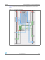
Electrical schematics
Electrical schematics
Figure 14. STM32F0DISCOVERY
37/41
100nF
3V
1
2
R21
R20
8MHz
X1
R19
1
2
3
4
5
0
5075BMR-05-SM
VCC
DD+
ID
GND
SHELL
CN1
U5V
USB
5V
3V
VBAT
PC13
PC14
PC15
OSCIN
OSCOUT
NRST
VSSA
VDDA
PA0
PA1
PA2
Not Fitted
STLINK_RX
1
2
3
4
5
6
7
8
9
10
11
12
EXT_5V
TX
RX
BAT60JFILM
R6
1K5
3V
R8
0
USB_DM
R7
0
USB_DP
R5
100K
D1
SB15
JP1
SB14
4K7
AIN_1
OSC_IN
OSC_OUT
STM_RST
4K7
C10
20pF
10K
Close to JP
Not Fitted
STM32F0_USART1_TX
PA9
PA10
STM32F0_USART1_RX
SB13
C8
R16
100K
C11
20pF
3V
Not Fitted
Board Ident: PC13=0
100K
R13
SWIM_IN
SWIM
10K
STLINK_TX
STM_JTCK
SWIM_IN
SWIM_RST
SWIM_RST_IN
48
47
46
45
44
43
42
41
40
39
38
37
3V
C6
100nF
C7
100nF
3V
36
35
34
33
32
31
30
29
28
27
26
25
C12
100nF
VDD_2
VSS_2
JTMS/SWDIO
PA12
PA11
PA10
PA9
PA8
PB15
PB14
PB13
PB12
VDD_3
VSS_3
PB9
PB8
BOOT0
PB7
PB6
PB5
PB4/JNTRST
PB3/JTDO
PA15/JTDI
JTCK/SWCLK
PA3
PA4
PA5
PA6
PA7
PB0
PB1
PB2/BOOT1
PB10
PB11
VSS_1
VDD_1
13
14
15
T_JTCK
16
T_JTDO
17
T_JTDI
18
T_NRST
T_JRST 19
20
SWIM_IN 21
22
SWIM
23
24
R18
C9
100nF
T_SWDIO_IN
T_JTMS
T_JTCK
STM_JTMS
USB_DP
USB_DM
T_SWO
LED_STLINK
3V
100
R34
R11
100
LD1
RED
R2
1K
3V
U2
STM32F103C8T6
1
2
3
4
5
6
R9
10K
R10
R17
R15
R14
R12
22
22
22
22
BAT60JFILM
D3
AIN_1
T_SWO
T_NRST
T_JTMS
T_JTCK
100
JP2
Idd
C24
20pF
VDD
MCO
Not Fitted
MCO
5V
3
1
COM
PWR
Vout
LED_STLINK
INH
GND
Vin
U1
T_SWO
SB22
T_NRST
CN2
SB11
SB9
SB7
SB5
STM_JTMS
STM_JTCK
SB19
5
100
R3
100
R4
3
2
4
1
R1
0
BAT60JFILM
D2
3V
Number:MB1034 Rev: B 0(PCB SCH)
Date: 2/3/2012
Sheet 2
3
SWD
of
STM32F0DISCOVERY ST-LINK/V2 (SWD only)
3V
OUT_3V
LD_BICOLOR_CMS
_Green
Red
LD2
STMicroelectronics
Title:
SWDIO
SWCLK
3V
PA14
PA13
NRST
PB3
Jumpers ON --> DISCOVERY Selected
Jumpers OFF --> ST-LINK Selected
SB12
SB10
SB8
SB6
DEFAULT
C1
C4
BYPASS
1μF_X5R_0603
1μF_X5R_0603
LD3985M33R
C3
C5
C2
10nF_X7R_0603
100nF
100nF
RC Must be very close to STM32F103 pin 29
Header 6
CN3
SWD
Not Fitted
2
Doc ID 022910 Rev 2
4
1
2
3
4
38/41
RESERVED
TCK/SWCLK
TMS/SWDIO
Electrical schematics
UM1525
Figure 15. ST-LINK/V2 (SWD only)
PC13
PC14
PC15
SB21
PF0
MCO
PF0
MCO
Not Fitted
Not Fitted
SB17
R25
0
2
1
X3
SB20
3
4
PA14
PA15
PC10
PC11
PC12
PD2
PB3
PB4
PB5
PB6
PB7
BOOT0
PB8
PB9
VSS_1
VDD_1
C15
6.8pF
R24
0
8MHz
C14
20pF
R23
0 X2
1
2
MC306-G-06Q-32.768 (JFVNY)
6.8pF
C16
49
50
51
52
53
54
55
56
57
58
59
60
61
62
63
64
SB1
PA14
PA15
PC10
PC11
PC12
PD2
PB3
PB4
PB5
PB6
PB7
BOOT0
PB8
PB9
VDD
SB18
C17
1uF
PB8
PB9
Close to XTAL & MCU
VBAT
PC13
PC14
PC15
510
10K
Close to STM32
SB2
R26
R27
Not Fitted
VDD
BOOT0
Not Fitted
PA14
PA15
PC10
PC11
PC12
PD2
PB3
PB4
PB5
PB6
PB7
PF7
PF6
PA13
PA12
PA11
PA10
PA9
PA8
PC9
PC8
PC7
PC6
PB15
PB14
PB13
PB12
PF7
PF6
PA13
PA12
PA11
PA10
PA9
PA8
PC9
PC8
PC7
PC6
PB15
PB14
PB13
PB12
48
47
46
45
44
43
42
41
40
39
38
37
36
35
34
33
VDD_2
VSS_2
PB11
PB10
PB2 or NPOR (1.8V mode)
PB1
PB0
PC5
PC4
PA7
PA6
PA5
PA4
PF5
PF4
PA3
PF7
PF6
PA13
PA12
PA11
PA10
PA9
PA8
PC9
PC8
PC7
PC6
PB15
PB14
PB13
PB12
C13
20pF
R22
390
SB16
PF1
PF1
PC3
PC3
PC2
PC2
PC1
PC1
PC0
PC0
NRST
NRST
PA2
PA1
PA0
VBAT
PC13 - TAMPER1 - WKUP2
PC14 - OSC32_IN
PC15 - OSC32_OUT
PF0 - OSC_IN
PF1 - OSC_OUT
NRST
PC0
PC1
PC2
PC3
VSSA / VREFVDDA / VREF+
PA0 - TAMPER2 - WKUP1
PA1
PA2
1
2
3
4
5
6
7
8
9
10
11
12
13
14
15
16
VDD
PB11
PB10
PB2
PB1
PB0
PC5
PC4
PA7
PA6
PA5
PA4
PF5
PF4
PA3
C18
1uF
VDD
PB11
PB10
PB2
PB1
PB0
PC5
PC4
PA7
PA6
PA5
PA4
PF5
PF4
PA3
PA2
PA1
PA0
VDD
32
31
30
29
28
27
26
25
24
23
22
21
20
19
18
17
U3
STM32F051R8T6
C20
100nF
C21
C19
100nF 100nF
VDD
PA0
blue
LD4
NRST
330
R33
100K
VDD
100
R32
VDD
R29
220K
Date: 3/1/2012
STM32F0DISCOVERY MCU
Number:MB1034 Rev: B.0(PCB.SCH)
Title:
B1
B2
SW-PUSH-CMS
RESET Button
USER & WAKE-UP Button
SB3
R28
100nF
C22
100nF
C23
SB4
Not Fitted
Not Fitted
660
R31
green
LD3
STMicroelectronics
PC8
330
2
1
3
4
2
1
Doc ID 022910 Rev 2
3
4
R30
SW-PUSH-CMS
PC9
Sheet 3
of
3
UM1525
Electrical schematics
Figure 16. MCU
39/41
Revision history
8
UM1525
Revision history
Table 12.
40/41
Document revision history
Date
Revision
Changes
20-Mar-2012
1
Initial release.
30-May-2012
2
Added Section 5: Connecting modules on the prototyping board on
page 27.
Doc ID 022910 Rev 2
UM1525
Please Read Carefully:
Information in this document is provided solely in connection with ST products. STMicroelectronics NV and its subsidiaries (“ST”) reserve the
right to make changes, corrections, modifications or improvements, to this document, and the products and services described herein at any
time, without notice.
All ST products are sold pursuant to ST’s terms and conditions of sale.
Purchasers are solely responsible for the choice, selection and use of the ST products and services described herein, and ST assumes no
liability whatsoever relating to the choice, selection or use of the ST products and services described herein.
No license, express or implied, by estoppel or otherwise, to any intellectual property rights is granted under this document. If any part of this
document refers to any third party products or services it shall not be deemed a license grant by ST for the use of such third party products
or services, or any intellectual property contained therein or considered as a warranty covering the use in any manner whatsoever of such
third party products or services or any intellectual property contained therein.
UNLESS OTHERWISE SET FORTH IN ST’S TERMS AND CONDITIONS OF SALE ST DISCLAIMS ANY EXPRESS OR IMPLIED
WARRANTY WITH RESPECT TO THE USE AND/OR SALE OF ST PRODUCTS INCLUDING WITHOUT LIMITATION IMPLIED
WARRANTIES OF MERCHANTABILITY, FITNESS FOR A PARTICULAR PURPOSE (AND THEIR EQUIVALENTS UNDER THE LAWS
OF ANY JURISDICTION), OR INFRINGEMENT OF ANY PATENT, COPYRIGHT OR OTHER INTELLECTUAL PROPERTY RIGHT.
UNLESS EXPRESSLY APPROVED IN WRITING BY TWO AUTHORIZED ST REPRESENTATIVES, ST PRODUCTS ARE NOT
RECOMMENDED, AUTHORIZED OR WARRANTED FOR USE IN MILITARY, AIR CRAFT, SPACE, LIFE SAVING, OR LIFE SUSTAINING
APPLICATIONS, NOR IN PRODUCTS OR SYSTEMS WHERE FAILURE OR MALFUNCTION MAY RESULT IN PERSONAL INJURY,
DEATH, OR SEVERE PROPERTY OR ENVIRONMENTAL DAMAGE. ST PRODUCTS WHICH ARE NOT SPECIFIED AS "AUTOMOTIVE
GRADE" MAY ONLY BE USED IN AUTOMOTIVE APPLICATIONS AT USER’S OWN RISK.
Resale of ST products with provisions different from the statements and/or technical features set forth in this document shall immediately void
any warranty granted by ST for the ST product or service described herein and shall not create or extend in any manner whatsoever, any
liability of ST.
ST and the ST logo are trademarks or registered trademarks of ST in various countries.
Information in this document supersedes and replaces all information previously supplied.
The ST logo is a registered trademark of STMicroelectronics. All other names are the property of their respective owners.
© 2012 STMicroelectronics - All rights reserved
STMicroelectronics group of companies
Australia - Belgium - Brazil - Canada - China - Czech Republic - Finland - France - Germany - Hong Kong - India - Israel - Italy - Japan Malaysia - Malta - Morocco - Philippines - Singapore - Spain - Sweden - Switzerland - United Kingdom - United States of America
www.st.com
Doc ID 022910 Rev 2
41/41