1
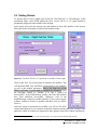
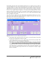
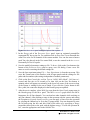
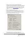
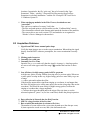
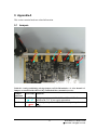
User's Manual Digital Gamma Finder (DGF) Pixie-500 Version 2.50, June 2012 XIA LLC 31057 Genstar Road Hayward, CA 94544 USA Phone: (510) 401-5760; Fax: (510) 401-5761 http://www.xia.com Disclaimer Information furnished by XIA is believed to be accurate and reliable. However, XIA assumes no responsibility for its use, or for any infringement of patents, or other rights of third parties, which may result from its use. No license is granted by implication or otherwise under the patent rights of XIA. XIA reserves the right to change the DGF product, its documentation, and the supporting software without prior notice. Table of Contents 1 Overview............................................................................................................................................3 1.1 Features of the Pixie-500............................................................................................................3 1.2 Specifications..............................................................................................................................3 1.3 Important Notes on Power Consumption....................................................................................4 2 Setting Up..........................................................................................................................................4 2.1 Installation..................................................................................................................................4 2.2 Getting Started............................................................................................................................7 3 Navigating the Pixie Viewer.............................................................................................................10 3.1 Overview...................................................................................................................................10 3.2 Optimizing Parameters..............................................................................................................10 4 Data Runs and Data Structures.........................................................................................................13 4.1 Run Types.................................................................................................................................13 4.2 Output Data ..............................................................................................................................13 4.3 Input/Output Parameters ..........................................................................................................13 5 Hardware Description.......................................................................................................................15 6 Theory of Operation.........................................................................................................................15 7 Operating Multiple Pixie-500 Modules Synchronously....................................................................15 8 Troubleshooting...............................................................................................................................16 8.1 Startup Problems.......................................................................................................................16 8.2 Acquisition Problems................................................................................................................20 9 Appendix A......................................................................................................................................22 9.1 Jumpers....................................................................................................................................22 9.2 PXI backplane pin functions....................................................................................................23 9.3 Control and Status Register Bits..............................................................................................24 2 Pixie-500 User’s Manual V2.50 XIA 2012. All rights reserved. 1 Overview This manual describes the DGF Pixie-500, a 4-channel all-digital waveform acquisition and spectrometer card based on the CompactPCI/PXI standard. The Pixie-500 currently comes in a 12-bit, 500 MHz version and a 14-bit, 400 MHz version. Since for both versions most of the design and operating principles are the same as for the DGF Pixie-4, this manual focuses on the differences to the Pixie-500. Users are referred to the Pixie-4 User manual for more detailed descriptions. Significant difference for the Pixie-500 are highlighted 1.1 Features of the Pixie-500 • • • • • • • Designed for high precision γ-ray spectroscopy with fast radiation detectors, e.g. scintillator/PMT combinations (NaI, LaBr3, etc) and many others. 12 bit, 500 MHz or 14bit, 400 MHz ADC resulting in energy resolutions close to HPGe capabilities. Simultaneous amplitude measurement and pulse shape analysis for each channel. Programmable gain (high/low) and input offset. Programmable pileup inspection criteria include trigger filter parameters, threshold, and rejection criteria. Triggered synchronous waveform acquisition across channels, modules and crates. Supports 32-bit 33 MHz PCI data transfers (>100 Mbytes/second). 1.2 Specifications Front Panel I/O Signal Input (4x) Logic Input/Output Logic Output 4 analog inputs. Selectable input impedance: 50Ω and 8.5kΩ ±5V pulsed, ±2V DC. Selectable input attenuation 1:8.8 and 1:1 for either impedance setting. General Purpose I/O connected to programmable logic. Currently can be either used as input for global backplane signals Veto or Status, or as an input for module specific logic level reported in the data stream, or as an external trigger. General Purpose output from Digital Signal Processor. Function to be determined. Backplane I/O Clock Input/Output Triggers Status Token Synch Veto Distributed 37.5 MHz clock on PXI backplane. Two wired-or trigger buses on PXI backplane. One for synchronous waveform acquisition, one for event triggers. Global logic level from backplane reported for each event Global logic level from backplane used for coincidence tests Wired-or SYNC signal distributed through PXI backplane to synchronize timers and run start/stop to 50ns. Global logic level to suppress event triggering. 3 Pixie-500 User’s Manual V2.50 XIA 2012. All rights reserved. Channel Gate Individual GATE to suppress event triggering for each channel with use of PXI-PDM (not yet implemented) Data Interface PCI 32-bit, 33MHz Read/Write, memory readout rate to host over 100 Mbytes/s. Digital Controls Gain Offset Shaping Trigger Analog switched gain of 1.0 or 2.9 Digital gain adjustment of up to ±10% in 15ppm steps. DC offset adjustment from –2.5V to +2.5V, in 65535 steps. Digital trapezoidal filter. Rise time and flat top set independently in small steps. Digital trapezoidal trigger filter with adjustable threshold. Rise time and flat top set independently. Data Outputs Spectrum Statistics Event data 1024-32768 channels, 32 bit deep (4.2 billion counts/bin). Additional memory for sum spectrum for clover detectors. Real time, live time, filter and gate dead time, input and throughput counts. Pulse height (energy), timestamps, pulse shape analysis results, waveform data and ancillary data like hit patterns. 1.3 Important Notes on Power Consumption A Pixie-500 module consumes roughly 25W which eventually is turned into heat in the chassis. Some elements of the board will get very hot, for example the ADCs alone consume ~2W each and will be too hot to touch. The chassis therefore has to have sufficient cooling capacity to keep the operating temperature in a reasonable range. It is strongly recommended to keep the chassis fan in the “high” setting if the chassis has such an option. Some chassis may provide overall less power than required to operate a Pixie-500 module in each slot. Please contact XIA for recommendations on which chassis are suitable for large multi-module systems. 2 Setting Up 2.1 Installation 2.1.1 Hardware Setup The Pixie-500 modules can be operated in any standard 3U CompactPCI or PXI chassis. Chassis following only the CompactPCI standard can be used to operate modules individually. To operate several modules together, a backplane following the PXI standard must be present. Put the host computer (or remote controller) in the system slot of your chassis. Place the Pixie-500 modules into any free slots with the chassis still powered down, 4 Pixie-500 User’s Manual V2.50 XIA 2012. All rights reserved. then power up the chassis (Pixie-500 modules are not hot swappable). If using a remote controller, be sure to boot the host computer after powering up the chassis1. 2.1.2 Drivers and Software System Requirements: The Pixie software is compatible with Windows XP, Vista, or Windows 7. For the 64 bit version of Windows 7, the PC's RAM must be 4 GB or less. Please contact XIA for details on operating Pixie-500 modules with Linux. When the host computer is powered up the first time after installing the controller and Pixie-500 modules in the chassis, it will detect new hardware and try to find drivers for it. (A Pixie-500 module will be detected as a new device every time it is installed in a new slot.) While there is no required order of installation of the driver software, the following sequence is recommended (users with embedded host computer skip to step 4): 1. If you have a remote controller, first install the driver software for the controller itself. Otherwise, skip to step 4. Unless directed otherwise by the manufacturer of the controller, this can be done with or without the controller and Pixie-500 modules installed in the host computer and/or chassis. If the modules are installed, ignore attempts by Windows to install drivers until step 7. NI controllers come with a multi-CD package called “Device Driver Reference CD”. For simplicity it is recommended to install the software on these CDs in the default configuration. 2. Unless already installed, power down the host computer, install the controller in both the host computer and chassis, and power up the system again (chassis first). 3. Windows will detect new hardware (the controller) and should find the drivers automatically. Verify in Window’s device manager that the controller is properly installed and has no “resource conflicts”. 4. Install Igor Pro 5. Install the Pixie-500 software provided by XIA (see section 2.1.3) 6. Unless already installed, power down the host computer and install the Pixie-500 modules in the chassis. Check the input jumper settings for the appropriate signal termination: 50 Ω or 5 kΩ (see section 9.1 for details). Then power up the system again (chassis first). 7. Windows will detect new hardware (the Pixie-500 modules) and should find the drivers automatically. If not, direct it to the “drivers” directory in the Pixie-500 software distribution installed in step 5. Verify in Window’s device manager that the modules are properly installed as “PLX Custom (OEM) PCI 9054 Boards (32)” or “... (64)” and have no “resource conflicts”. Currently, the driver must be version 6.5.0.2 1 In some systems, “scan for hardware changes” in the Windows device manager may detect and install a remote chassis when the PC was booted first. 2 For information on using the older PLX drivers (version 6.3.1) with Windows 2000, see the “readme” file in the Drivers folder of the software distribution. 5 Pixie-500 User’s Manual V2.50 XIA 2012. All rights reserved. 2.1.3 Pixie User Interface The Pixie Viewer, XIA’s graphical user interface to set up and run the Pixie-500 modules, is based on WaveMetrics’ IGOR Pro. To run the Pixie Viewer, you have to have IGOR Version 5.0 or higher installed on your computer. By default, IGOR Pro will be installed at C:\Program Files\WaveMetrics\IGOR Pro Folder. The CD-ROM with the Pixie-500 software distribution contains 1. an installation program Setup.exe, 2. the Pixie-500 software in the folder XIA\Pixie500 and its subfolders. For the 400 MHz variant, the folder is named Pixie400. The Pixie-500 software can be installed by running its installation program. Follow the instructions shown on the screen to install the software to the default folder selected by the installation program, or to a custom folder. This folder will contain the IGOR control program (Pixie500.pxp or Pixie400.pxp), online help files and 8 subfolders (Configuration, Doc, Drivers, DSP, Firmware, MCA, PixieClib, and PulseShape). Make sure you keep this folder organization intact, as the IGOR program and future updates rely on this. Feel free, however, to add folders and subfolders at your convenience. 6 Pixie-500 User’s Manual V2.50 XIA 2012. All rights reserved. 2.2 Getting Started To start the Pixie Viewer, double-click on the file “Pixie500.pxp” or “Pixie400.pxp” in the installation folder. After IGOR loaded the Pixie Viewer, the START UP3 panel should be prominently displayed in the middle of the desktop. In the panel, first select the chassis type and number of Pixie-500 modules in the system. Then specify the slot number in which each module resides. Figure 2.1: The Pixie-500 START UP panel (above) and MAIN Panel (right) Click on the Start Up System button to initialize the modules. This will download DSP code and FPGA configuration to the modules, as well as the module parameters. Due to the large size of the FPGA, it will take ~5s per module to complete the download. If you see messages similar to “Module 0 in slot 5 started up successfully!” in the IGOR history window, the Pixie-500 modules have been initialized successfully. Otherwise, refer to the troubleshooting section for possible solutions. If you want to try the software without a chassis or modules attached, click on Offline Analysis. After the system is initialized successfully, you will see the MAIN control panel that serves as a shortcut to the most common actions and from which all other panels are called. Its controls are organized in three groups: Setup, Run Control, and Results. 3 In the following, SMALL CAPS are used for panel names; italic font is used for buttons and controls. 7 Pixie-500 User’s Manual V2.50 XIA 2012. All rights reserved. In the Setup group, the Start System button opens the START UP panel in case you need to reboot the modules. The Open Panels popup menu leads to four panels where parameters and acquisition options are entered. They are described in more detail in section 3 and in the online help. To get started, select Parameter Setup, which will open (or bring to front) the PARAMETER SETUP panel shown in Figure 2.2. For most of the actions the Pixie Viewer interacts with one Pixie module at a time. The number of that module is displayed at the top of the MAIN panel and the top right of the PARAMETER SETUP panel. Proceed with the steps below to configure your system. Note: The More/Less button next to the Help button on the bottom of the PARAMETER SETUP panel can be used to hide some controls. This may be helpful to first-time Pixie users who only want to focus on the most essential settings. For an initial setup, go through the following steps: Figure 2.2: The PARAMETER SETUP Panel, Energy tab shown 1. If not already visible, open the PARAMETER SETUP panel by selecting Parameter Setup from the Open Panel popup menu in the MAIN panel. 2. At the bottom of the PARAMETER SETUP panel, click on the Oscilloscope button. This opens a graph that shows the untriggered signal input. In the OSCILLOSCOPE panel, click Refresh to update the display. The pulses should fall in the display range (0-4K for the 500 MHz version, 0-16K for the 400 MHz version). If no pulses are visible or if they are cut off at the upper or lower range of the display, click Adjust Offsets to automatically set the DC offset. If the pulse amplitude is too large to fall in the display range, decrease the Gain. If the pulses are negative, toggle the Invert checkbox. 8 Pixie-500 User’s Manual V2.50 XIA 2012. All rights reserved. Figure 2.3: OSCILLOSCOPE panel with typical pulses from a pulser. 3. In the Energy tab of the PARAMETER SETUP panel, input an estimated preamplifier exponential RC decay time for Tau, and then click on Auto Find Tau to determine the actual Tau value for all channels of the current module. You can also enter a known good Tau value directly in the Tau control field, or use the controls in the OSCILLOSCOPE to manually fit Tau for a pulse. 4. Save the modified parameter settings to file. To do so, click on the Save button at the bottom of the PARAMETER SETUP panel to open a save file dialog. Create a new file name to avoid overwriting the default settings file. 5. Save the Igor experiment using File -> Save Experiment As from the top menu. This saves the current state of the interface with all open panels and the settings for file paths and slot numbers (the settings independent of module parameters). 6. Click on the Run Control tab, set Run Type to “0x301 MCA Mode”, Poll time to 1 second, and Run time to 30 seconds or so, then click on the Start Run button. A spinning wheel will appear occasionally in the lower left corner of the screen as long as the system is waiting for the run to finish. If you click the Update button in the MAIN panel, the count rates displayed in the Results group are updated. 7. After the run is complete, select MCA Spectrum from the Open Panels popup menu in the Results group of the MAIN panel. The MCA SPECTRUM graph shows the MCA histograms for all four channels. You can deselect other channels while working on only one channel. After defining a range in the spectrum with the cursors and setting the fit option to fit peaks between cursors, you can apply a Gauss fit to the spectrum by selecting the channels to be fit in the Fit popup menu. You can alternatively enter the fit limits using the Min and Max fields in the table or by specifying a Range around the tallest peak or the peak with the highest energy. To scale the spectrum in keV, enter the appropriate ratio in the field keV/bin. 9 Pixie-500 User’s Manual V2.50 XIA 2012. All rights reserved. At this stage, you may not be able to get a spectrum with good energy resolutions. You may need to adjust some settings such as energy filter rise time and flat top as described in section 3.2. 3 Navigating the Pixie Viewer 3.1 Overview The Pixie Viewer consists of a number of graphs and control panels, linked together by the MAIN control panel. The Viewer comes up in exactly the same state as it was when last saved to file using File->Save Experiment. This preserves settings such as the file paths and the slot numbers entered in the START UP panel. However, the Pixie module itself loses all programming when it is switched off. When the Pixie module is switched on again, all programmable components need code and configuration files to be downloaded to the module. The Pixie Viewer is described in more detail in the Pixie-4 User manual (section 3). Detailed information on the individual controls can also be found in the Online Help for each panel. 3.2 Optimizing Parameters Optimization of the Pixie-500’s run parameters for best resolution depends on the individual systems and usually requires some degree of experimentation. The Pixie Viewer includes several diagnostic tools and settings options to assist the user, as described below. 3.2.1 Noise For a quick analysis of the electronic noise in the system, you can view a Fourier transform of the incoming signal by selecting OSCILLOSCOPE FFT. The graph shows the FFT of the untriggered input sigal of the OSCILLOSCOPE. By adjusting the dT control in the OSCILLOSCOPE and clicking the Refresh button, you can investigate different frequency ranges. For best results, remove any source from the detector and only regard traces without actual events. If you find sharp lines in the 10 kHz to 1 MHz region you may need to find the cause for this and remove it. If you click on the Apply Filter button, you can see the effect of the energy filter simulated on the noise spectrum. 3.2.2 Energy Filter Parameters The main parameter to optimize energy resolution is the energy filter rise time. Generally, longer rise times result in better resolution, but reduce the throughput. Optimization should begin with scanning the rise time through the available range. Try 2µs, 4µs, 8µs, 11.2µs, take a run of 60s or so for each and note changes in energy resolution. Then fine tune the rise time. The flat top usually needs only small adjustments. For a typical coaxial Ge-detector we suggest to use a flat top of 1.2µs. For a small detector (20% efficiency) a flat top of 0.8µs is a 10 Pixie-500 User’s Manual V2.50 XIA 2012. All rights reserved. good choice. For larger detectors flat tops of 1.2µs and 1.6µs will be more appropriate. In general the flat top needs to be wide enough to accommodate the longest typical signal rise time from the detector. It then needs to be wider by one filter clock cycle than that minimum, but at least 3 filter clock cycles. Note that a filter clock cycle ranges from 0.026 to 0.853µs, depending on the filter range, so that it is not possible to have a very short flat top together with a very long filter rise time. The Pixie Viewer provides a tool which automatically scans all possible combinations of energy filter rise time and flat top and finds the combination that gives the best energy resolution. This tool can be accessed by clicking the Optimize button on the Settings tab. Please refer to the Online Help documentation for more details. A second option is to create a file series where the energy filter parameters are modified for each file in the series. See section 3.6 for more details. 3.2.3 Threshold and Trigger Filter Parameters In general, the trigger threshold should be set as low as possible for best resolution. If too low, the input count rate will go up dramatically and “noise peaks” will appear at the low energy end of the spectrum. If the threshold is too high, especially at high count rates, low energy events below the threshold can pass the pile-up inspector and pile up with larger events. This increases the measured energy and thus leads to exponential tails on the (ideally Gaussian) peaks in the spectrum. Ideally, the threshold should be set such that the noise peaks just disappear. The settings of the trigger filter have only minor effect on the resolution. However, changing the trigger conditions might have some effect on certain undesirable peak shapes. A longer trigger rise time allows the threshold to be lowered more, since the noise is averaged over longer periods. This can help to remove tails on the peaks. A long trigger flat top will help to trigger better on slow rising pulses and thus result in a sharper cut off at the threshold in the spectrum. 3.2.4 Decay Time The preamplifier decay time τ is used to correct the energy of a pulse sitting on the falling slope of a previous pulse. The calculations assume a simple exponential decay with one decay constant. A precise value of τ is especially important at high count rates where pulses overlap more frequently. If τ is off the optimum, peaks in the spectrum will broaden, and if τ is very wrong, the spectrum will be significantly blurred. The first and usually sufficiently precise estimate of τ can be obtained from the Auto Find routine in the Energy tab of the PARAMETER SETUP panel. Measure the decay time several times and settle on the average value. Fine tuning of τ can be achieved by exploring small variations around the fit value (±2-3%). This is best done at high count rates, as the effect on the resolution is more pronounced. The value of τ found through this way is also valid for low count rates. Manually enter τ , take a short run, and note the value of τ that gives the best resolution. Pixie users can also use the fit routines in the OSCILLOSCOPE to manually find the decay time through exponentially fitting the untriggered input signals. Another tool is the Optimize 11 Pixie-500 User’s Manual V2.50 XIA 2012. All rights reserved. routine in the Energy tab of the PARAMETER SETUP panel. Similar to the routine for finding the optimal energy filter times, this routine can be used to automatically scan a range of decay times and find the optimal one. Please refer to the Online Help documentation for more details. A further option is to create a file series where τ is modified for each file in the series. See section 3.6 of the Pixie-4 user manual for more details. 12 Pixie-500 User’s Manual V2.50 XIA 2012. All rights reserved. 4 Data Runs and Data Structures 4.1 Run Types There are two major run types: MCA runs and List mode runs. MCA runs only collect spectra, List mode runs acquire data on an event-by event basis, but also collect spectra. List mode runs come in several variants, storing different amounts of data per event. The run types and data formats are described in detail in the Pixie-4 User manual. 4.2 Output Data The only differences in output data for the Pixie-500 are the definition of the following list mode data words: – The “BUF_FORMAT” word in the buffer header is formed by adding 0x4000 to the run task in the 500 MHz version and by adding 0x5000 for the 400 MHz version. 4 The Buffer header is thus as shown in Table 4.1. This allows data processing software to distinguish Pixie-4 data from Pixie-500 data digitized at different rates – All timestamps in the buffer header, event header and channel header are in units of 2 ns (500 MHz) or 2.5 ns (400 MHz). The smallest increment of timestamps is 8ns (10ns for 400 MHz version). Optionally, buffer header and event header time stamps can be in units of 13.33ns (e.g. to match timing in a Pixie-4 module). The option is controlled by a checkbox in the Run Tab of the Pixie Viewer. – Time intervals between the waveform samples are 2 ns (500 MHz) or 2.5 ns (400 MHz). – If pulse shape analysis is performed to compute the constant fraction time of arrival, the result “CHAN_XIAPSA” is still in units of 1/256 of a sample interval, but a sample interval is 2 ns or 2.5 ns. For example, if CHAN_XIAPSA = 0x0509 in a 500 MHz system, the CFD time is 5 + 9/256 ADC sample steps or 10.0703 ns away from the beginning of the recorded trace – There are no flags for special events recorded in the CHAN_USERPSA word. Note: The Run start time in the buffer header and the event time in the event header are in units of 13.3ns as in the Pixie-4. Table 4.1: Buffer header data format for the Pixie-500. Word # 0 1 2 Variable BUF_NDATA BUF_MODNUM BUF_FORMAT 3 BUF_TIMEHI Description Number of words in this buffer Module number Format descriptor = RunTask + 0x40T0 or 0x50T0 T: bits4-7 indicate channel 0-3 acquired waveforms in 4x trace mode. Run start time, high word 4 Yes, 4/5 do not match 13 Pixie-500 User’s Manual V2.50 XIA 2012. All rights reserved. 4 5 BUF_TIMEMI BUF_TIMELO Run start time, middle word Run start time, low word 4.3 Input/Output Parameters Most of the Pixie-500 input and output parameters are the same as in the Pixie-4. A full description is provided in the Programmer Manual. In table 4.2 we list those parameters that are different for the Pixie-500. Most of these differences are handled in the Pixie C library. For example, while the energy filter in the Pixie-500 operate on a 8ns time scale (vs 13.3ns in the Pixie-4), user still enter the filter time in µs and the only effect visible to the user is the step size of the allowed filter values. Table 4.2: Input/output parameter differences between Pixie-4 and Pixie-500. (If parameter names in the Pixie Viewer different from the C/DSP parameters name, is is shown in parentheses) Parameter FILTERRANGE Range for energy filter rise time or flat top in FILTERRANGE =F CHANCSRA, B, C (checkboxes) Pixie-4 Legal values 1-6 Pixie-500, 500 MHz Legal values 1-6 Pixie-500, 400 MHz Legal values 1-6 2x13.3ns*2F 127x13.3ns*2F 2x8ns*2F - 127x8ns*2F 2x10ns*2F 127x10ns*2F SGA (gain) Bit 0-7 are used to switch from 0.8511.25 Legal values 2-63 (time in ns is FASTLENGTH * 13.3ns) Legal values 0-63 (time in ns is FASTGAP * 13.3ns) Legal values 0-1024 (time in ns is TRACELENGTH * 13.3ns, i.e. range is 0-13.6µs) Control bits for – GATE are ignored Bit 0 is used to switch from 1.0 to 2.9 Control bits for – GATE are ignored Bit 0 is used to switch from 1.0 to 2.9 Legal values 2-63 (time in ns is FASTLENGTH * 8ns) Legal values 2-63 (time in ns is FASTLENGTH * 10ns) Legal values 0-63 (time in ns is FASTGAP * 8ns) Legal values 0-8192 (time in ns is TRACELENGTH * 2ns, i.e. range is 0-16.4µs)) ignored ignored Three 16 bit words form a 48 bit number in units of 8ns*32 Three 16 bit words form a 48 bit number in units of 8ns Three 16 bit words form a 48 bit number in units of 8ns*32 Legal values 0-63 (time in ns is FASTGAP * 10ns) Legal values 0-8192 (time in ns is TRACELENGTH * 2.5ns, i.e. range is 0-20.48µs)) ignored ignored Three 16 bit words form a 48 bit number in units of 10ns*32 Three 16 bit words form a 48 bit number in units of 10ns Three 16 bit words form a 48 bit number in units of 10ns*32 FASTLENGTH (trigger filter rise time) FASTGAP (trigger filter flat top) TRACELENGTH GATEDELAY GATEWINDOW LIVETIMEA,B,C (Livetime) FTDTA,B,C (Fast trigger dead time) SFDTA,B,C (slow filer dead time) Three 16 bit words form a 48 bit number in units of 13.3ns*16 Three 16 bit words form a 48 bit number in units of 13.3ns Three 16 bit words form a 48 bit number in units of 13.3ns*16 14 Pixie-500 User’s Manual V2.50 XIA 2012. All rights reserved. GDTA,B,C (gate dead time) Three 16 bit words form a 48 bit number in units of 13.3ns*16 ignored 15 ignored Pixie-500 User’s Manual V2.50 XIA 2012. All rights reserved. 5 Hardware Description The Pixie-500 is a 4-channel unit designed for gamma-ray spectroscopy and waveform capturing. The functional building blocks are similar to the Pixie-4, please refer to the Pixie-4 User manual for details. The main difference is the use of a faster ADC and FPGA to process the ADC data stream as indicated in Figure 5.1. When using external signals, note that the Pixie-500 MMCX inputs are labeled correctly as DSP OUT and IN/OUT. For Pixie-4 modules, the labels are swapped. On the Pixie-500, an external input signal should therefore be connected to the IN/OUT connector (not DSP OUT as described in the Pixie-4 manual) analog gaingand an a log ain offset, MHz and250 offs et Nyquist 500 MSPS ADC analo g gai n and o ffs et 1500 4b it MSPS AADC DC analo g gai n and o ffs et 500 MSPS ADC analo g gai n and o ffs et 1500 4b it MSPS AADC DC Veto 3 2 bit, 3 3M H z PCI FPG A Vir tex 4 P CI I/O ( J1 ) S ystem F PG A D SP PLL, VCO, phase MCA, LM memory clock, trigger (J2) OSC 37.5 Figure 5.1: Functional block diagram of the Pixie-500 front-end data acquisition and signal processing card. The ADCs are either 12bit, 500 MHz or 14bit, 400 MHz models. 6 Theory of Operation The principles of operation for the Pixie-500 are the same as for the Pixie-4. Please refer to the Pixie-4 User manual for a detailed description. 7 Operating Multiple Pixie-500 Modules Synchronously When many Pixie-500 modules are operating as a system, it may be required to synchronize clocks and timers between them and to distribute triggers across modules. It will also be necessary to ensure that runs are started and stopped synchronously in all modules. All these signals are distributed through the PXI backplane and follow the same principles as in the Pixie-4. Please see the Pixie-4 user manual for a detailed description. Significant differences in the Pixie-500 are 16 Pixie-500 User’s Manual V2.50 XIA 2012. All rights reserved. – Trigger distribution across PXI bus boundaries is currently not implemented – Gate signals for individual channels are currently ignored 8 Troubleshooting 8.1 Startup Problems 1. Computer does not boot when Pixie module is installed in chassis This is usually caused by an incorrect clock setting on the Pixie module. The module needs to have a valid clock to respond to the computer’s scanning of the PCI bus. 2. Computer reports new hardware found, needs driver files Whenever a Pixie module is installed in a slot of the chassis for the first time, it is detected as new hardware, even if Pixie modules have been installed in other slots previously. Point Windows to the driver files provides with the software distribution. After driver installation, the module should appear in Window’s Device Manager as in the picture below: 17 Pixie-500 User’s Manual V2.50 XIA 2012. All rights reserved. 3. Windows can not use drivers due to problem in digital signing This problem seems most common in Windows 7. The PLX drivers currently only “inofficially” support Windows 7. While this is being addressed, a workaround solution is to install the complete PLX software development kit (SDK), which seems to install the PLX drivers in a way acceptable to Windows 7. The SDK is available for free from PLX (http://www.plxtech.com), but registration is required. 4. Drivers are installed, but module does not boot The Pixie-500 modules require driver version 6.5.0 provided by XIA, not the earlier versions (6.3.1, 5.2, 4.1 or 4.4). Modules should be listed in Window’s device manager as “PLX Custom (OEM) PCI 9054 Board (32)” or “... (64)”. If the “PLX” is missing, it indicates driver version 4.1 is used. A picture of the driver information reported by Windows is shown below 5. When starting the Pixie Viewer, IGOR reports compile error For IGOR to start up properly, a number of driver files have to be in the correct 18 Pixie-500 User’s Manual V2.50 XIA 2012. All rights reserved. locations. In particular, the file “pixie.xop” has to be located in the “Igor Extensions” folder – usually C:\Program Files\Wavemetrics\Igor Pro\Igor Extensions in a default installation – and the file “PlxApi631.dll” has to be in C:\Windows\System32. 6. When starting up modules in the Pixie Viewer, downloads are not “successful” This can have a number of reasons. Verify that - The files and paths point to valid locations (run the “UseHomePaths” macro) - The slot numbers entered in the Startup panel match the location of the modules. - The correct drivers are used (version 6.4.2) and modules are recognized in Window’s Device Manager as shown above 8.2 Acquisition Problems 1. Signal from PMT shows unusual pulse shape Verify the input jumpers are set to the correct termination. When taking the signal directly from the PMT without a preamplifier, the correct termination is usually 50Ω 2. Missing peaks in spectra 3. Unusually low count rate 4. Unusually low Live Time Open the OSCILLOSCOPE and verify that the signal is in range, i.e. that large pulses are not cut off at the upper end of the range (4K) and that the baseline is above zero 5. Low efficiency for high energy peaks in MCA spectrum At high rates, pulses overlap with the decaying tail of a previous pulse. When two or more pulses overlap in this way, higher energy pulses are more likely to go out of range => reduce gain and/or adjust the offset If the detector output shows significant ringing or overshoots, it can happen that the Pixie-500 triggers twice on the same pulse (first on the rising edge, then on the overshoot). This would be more likely for higher energy pulses, because the ringing or overshoot has a larger amplitude. => increase the trigger threshold and/or the trigger filter rise time or use the advanced options to “pause” or (for low count rates) disable the pileup inspection. 6. Data collection in list mode has low DAQ fraction 7. SFDT is a large fraction of the live time 8. Rate at which list mode data is written to file is low The number of events collected in a given time depends on a) the data per event, b) time required to record an event, and c) the data transfer rate. 19 Pixie-500 User’s Manual V2.50 XIA 2012. All rights reserved. To reduce a), - run in compressed list mode (run types 0x101-103) - shorten the tracelength as much as possible (can be zero in 0x101-103) - remove the “read always” and “good channel” option for unused channels To reduce b) - reduce the coincidence window to the minimum possible - if no pulse shape analysis is required in compressed list mode runs, set the tracelength to zero - do not require pulse shape analysis To increase c) - run in 32x buffer or 16/16 double buffer mode - avoid frequent updates of run statistics and spectra - set the polling time to a small value (0.1-0.01) - verify the number of events/buffer is set to the maxium 9. Bad energy resolution in MCA spectrum - verify the decay time is set correctly - increase energy filter rise time - make the energy filter flat top approximately equal to the rise time of the pulse - ensure the “integrator” is set to zero - if “integrator” is set to 1 on purpose (e.g. fast scintillator pulses), make sure the energy filter flat top covers the entire pulse - if “integrator” is set to 2 on purpose (e.g. square pulses), make sure the energy filter flat top covers the portion of the pulse that should be disregarded for the energy measurement (e.g. the rising edge) 20 Pixie-500 User’s Manual V2.50 XIA 2012. All rights reserved. 9 Appendix A This section contains hardware-related information. 9.1 Jumpers Table 10.1: Analog conditioning selection jumpers on Pixie-500 modules. x=1..4 for channel 0..3. Jumpers are marked with solid red (50Ω) and dashed blue (attenuation) arrows. Jumper reference JPx01 PCB Label Function JPx02 “50” “ATTN” 3 pin jumper, pins are labeled “1” - middle - “1/8”. Connect middle with “1/8” if you require attenuation. Set for input impedance of 50Ω. If not set, input impedance is 8.5kΩ. 21 Pixie-500 User’s Manual V2.50 XIA 2012. All rights reserved. Table 10.2: On-board jumper settings for the clock distribution on Pixie-500 modules. Clock mode Single Module JP1 and JP2 Connect pins 2 and 3 of JP2 JP3 not set PCB Label LOC to IN Daisy-Chained Clock Master Daisy-Chained Clock Repeater Bussed Clock Master Bussed Clock Slave Clock Slave with PXI clock Clock Master for PXI clock (Revision C only) Connect pins 2 and 3 of JP2 not set LOC to IN Not set set Left Connect pins 2 and 3 of JP2 not set Connect pin1, JP1 to pin 1, JP2 Connect pins 1 and 2 of JP2 not set LOC to IN OUT to BUS BUS to IN Connect pin2, JP1 to pin 2, JP2 not set PXI to IN Connect pin2, JP1 to pin 2, JP2 not set Connect pin3, JP1 to pin 3, JP2 PXI to IN LOC to BP 9.2 PXI backplane pin functions Table 10.3: Pins of the J2 backplane connector defined in the PXI standard used by the Pixie500. Pins not listed are not connected except for pull-ups to 5V recommended by the PXI standard. J2 pin number 1A 3A 16A 17A 18A 19A 20A 21A PXI pin name LBL9 LBR7 TRIG1 TRIG2 TRIG3 LBL2 LBR4 LBR0 Connection Type Pixie pin function Left neighbor Right neighbor Bussed Bussed Bussed Left neighbor Right neighbor Right neighbor Event Trigger output (chained OR) reserved Event Trigger Veto Sync Sync output (chained OR) reserved Clock output 16B 18B 20B TRIG0 TRIG4 LBR5 Bussed Bussed Right neighbor Fast Trigger Status reserved 1C 3C 18C 19C 20C LBL10 LBR8 TRIG5 LBL3 LBL0 Left neighbor Right neighbor Bussed Left neighbor Left neighbor Fast Trigger output (chained OR) reserved Token Control data to PDM (left) Clock input 22 Pixie-500 User’s Manual V2.50 XIA 2012. All rights reserved. 2D 3D 15D 17D 19D 21D LBL7 LBR9 LBL6 STAR LBL4 LBR2 Left neighbor Right neighbor Left neighbor Star trigger to slot 2 Left neighbor Right neighbor GATE input channel 3 Event Trigger input (chained OR) GATE input channel 2 Hit pattern to slot 2 GATE input channel 0 Sync input (chained OR) 2E 3E 15E 16E 17E 19E 21E LBL8 LBR10 LBR6 TRIG7 CLK10 LBL5 LBR3 Left neighbor Right neighbor Right neighbor Bussed Clock Left neighbor Right neighbor reserved Fast Trigger input (chained OR) reserved Bussed Clock PXI Clock GATE input channel 1 reserved 9.3 Control and Status Register Bits Table 10.4: Control and Status Register of the Pixie-500 System FPGA 0x0001 Bit 0 RunEna 0x0002 0x0004 Bit 1 Bit 2 Unused PCIactive 0x0008 0x0010 Bit 3 Bit 4 Unused DSPReset 0x0020 Bit 5 0x0040 0x0080 0x0100 0x0200 0x0400 0x0800 0x1000 0x2000 0x4000 0x8000 Bit 6 Bit 7 Bit 8 Bit 9 Bit 10 Bit 11 Bit 12 Bit 13 Bit 14 Bit 15 Set to 1 to start data acquisition or 0 to stop. Automatically cleared when DSP de-asserts Active to end run. Reserved for future use. Set to reserve external memory I/O for host Reserved for future use. Write only. Set to reset DSP processor to initiate program download SynchCtrl Read only. If low, module is busy with run initialization, has filled its I/O buffer with data, or is finished with the run. Unused Reserved for future use. Unused Reserved for future use. SynchFlag Read only. Reserved for future use. Live* Read only. If zero, DSP is taking data. Unused Reserved for future use. Unused Reserved for future use. Unused Reserved for future use. Active Read only. If set, there is a run in progress. LAMState Read only. If set, LAM is set internally. Unused Reserved for future use. 23 Pixie-500 User’s Manual V2.50 XIA 2012. All rights reserved.