1
SECTION 10
MEMORY CONTROLLER
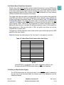
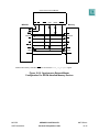
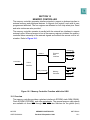
The memory controller generates interface signals to support a glueless interface to
external memory and peripheral devices. It supports four regions, each with its own
programmed attributes. The four regions are reflected on four chip-select pins. Read
and write strobes are also provided.
The memory controller operates in parallel with the external bus interface to support
external cycles. When an access to one of the memory regions is initiated, the memory
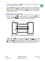
controller takes ownership of the external signals and controls the access until its termination. Refer to Figure 10-1.
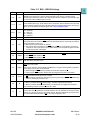
ADDR[0:31]
EBI Bus
Internal Bus
External
Bus
Interface
DATA[0:31]
Control Bus
U-bus
Interface
WE[0:3]/BE[0:3]
Memory Controller
Bus
Memory
Controller
OE
CS[0:3]
Figure 10-1 Memory Controller Function within the USIU
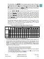
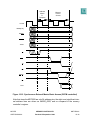
10.1 Overview
The memory controller provides a glueless interface to EPROM, static RAM (SRAM),
Flash EPROM (FEPROM), and other peripherals. The general-purpose chip-selects
are available on lines CS0 through CS3. CS0 also functions as the global (boot)
MPC555
USER’S MANUAL
MEMORY CONTROLLER
Revised 15 September 1999
MOTOROLA
10-1
chip-select for accessing the boot flash EEPROM. The chip select allows zero to 30
wait states.
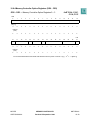
Figure 10-2 is a block diagram of the MPC555 memory controller.
.
INTERNAL ADDRESS(0:16),AT(0:2)
,
Base Register (BR)
Base Register (BR)
Base Register (BR)
Base Register (BR)
Base Register (BR)
Base Register (BR)
Base Register (BR)
Option Register (OR)
Dual Mapping
Base Register (DMBR)
Dual Mapping
Option Register (DMOR)
Region Match Logic
ATTRIBUTES
CS(0:3)
Expired
Wait State Counter
Load
WE/BE(0:3)
General-Purpose
Chip-Select
Machine
(GPCM)
OE
Figure 10-2 Memory Controller Block Diagram
Most memory controller features are common to all four banks. (For features unique
to the CS0 bank, refer to 10.4 Global (Boot) Chip-Select Operation.) A full 32-bit
address decode for each memory bank is possible with 17 bits having address masking. The full 32-bit decode is available, even if all 32 address bits are not sent to the
MPC555 pins.
MPC555
USER’S MANUAL
MEMORY CONTROLLER
Revised 15 September 1999
MOTOROLA
10-2
Each memory bank includes a variable block size of 32 Kbytes, 64 Kbytes and up to
4 Gbytes. Each memory bank can be selected for read-only or read/write operation.
The access to a memory bank can be restricted to certain address type codes for system protection. The address type comparison occurs with a mask option as well.
From zero to 30 wait states can be programmed with TA generation. Four byte-write
and read-enable signals (WE/BE(0:3)) are available for each byte that is written to
memory. An output enable (OE) signal is provided to eliminate external glue logic. A
memory transfer start (MTS) strobe permits one master on a bus to access external
memory through the chip selects on another.
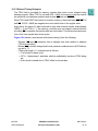
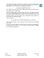
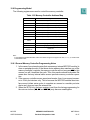
The memory controller functionality allows MPC555-based systems to be built with little or no glue logic. A minimal system using no glue logic is shown in Figure 10-3. In
this example CS0 is used for the 16-bit boot EPROM and CS1 is used for the 32-bit
SRAM. The WE/BE[0:3] signals are used both to program the EPROM and to enable
write access to various bytes in the RAM.
Address
Address
CE
CE
OE
OE
CS0
OE
WE/BE[0:1]
Data
DATA[0:15]
[0:15]
EPROM
MPC555
Address
CS1
CE
WE/BE[0:3]
WE/BE[0:3]
W
[0:31]
Data
OE
SRAM
Figure 10-3 MPC555 Simple System Configuration
10.2 Memory Controller Architecture
The memory controller consists of a basic machine that handles the memory access
cycle: the general-purpose chip-select machine (GPCM).
MPC555
USER’S MANUAL
MEMORY CONTROLLER
Revised 15 September 1999
MOTOROLA
10-3
When a new access to external memory is requested by any of the internal masters,
the address of the transfer (with 17 bits having mask) and the address type (with 3 bits
having mask) are compared to each one of the valid banks defined in the memory controller. Refer to Figure 10-4.
Base Address
Address Mask
RB ARB A RB A RB A RB A O O O O O O O O O RB A RB A
[0]
[1]
[2]
[3]
[4]
[15]
[16]
M
[0]
M
M
M
M
[1]
[2]
[3]
[4]
M
[5]
M
[6]
M
[7]
OOOO M
[16]
A[0:16]
M[0:16]
comp comp comp comp comp comp comp comp comp comp comp
Match
Figure 10-4 Bank Base Address and Match Structure
When a match is found on one of the memory banks, its attributes are selected for the
functional operation of the external memory access:
• Read-only or read/write operation
• Number of wait states for a single memory access, and for any beat in a burst
access
• Burst-inhibit indication. Internal burst requests are still possible during burst-inhibited cycles; the memory controller emulates the burst cycles
• Port size of the external device
Note that if more than one region matches the internal address supplied, then the lowest region is selected to provide the attributes and the chip select.
10.2.1 Associated Registers
Status bits for each memory bank are found in the memory control status register
(MSTAT). The MSTAT reports write-protect violations for all the banks.
Each of the four banks has a base register (BR) and an option register (OR). The BRx
and ORx registers contain the attributes specific to bank x. The base register contains
a valid bit (V) that indicates that the register information for that chip select is valid.
MPC555
USER’S MANUAL
MEMORY CONTROLLER
Revised 15 September 1999
MOTOROLA
10-4
10.2.2 Port Size Configuration
The memory controller supports dynamic bus sizing. Defined 8-bit ports can be
accessed as odd or even bytes. Defined 16-bit ports, when connected to data bus lines
zero to 15, can be accessed as odd bytes, even bytes, or even half-words. Defined 32bit ports can be accessed as odd bytes, even bytes, odd half-words, even half-words,
or words on word boundaries. The port size is specified by the PS bits in the base
register.
10.2.3 Write-Protect Configuration
The WP bit in each base register can restrict write access to its range of addresses.
Any attempt to write this area results in the associated WPER bit being set in the
MSTAT.
If an attempt to access an external device results in a write-protect violation, the memory controller considers the access to be no match. No chip-select line is asserted
externally, and the memory controller does not terminate the cycle. The external bus
interface generates a normal cycle on the external bus. Since the memory controller
does not acknowledge the cycle internally, the cycle may be terminated by external
logic asserting TA or by the on-chip bus monitor asserting TEA.
10.2.4 Address and Address Space Checking
The base address is written to the BR. The address mask bits for the address are written to the OR. The address type access value, if desired, is written to the AT bits in the
BR. The ATM bits in the OR can be used to mask this value. If address type checking
is not desired, program the ATM bits to zero.
Each time an external bus cycle access is requested, the address and address type
are compared with each one of the banks. If a match is found, the attributes defined
for this bank in its BR and OR are used to control the memory access. If a match is
found in more than one bank, the lowest bank matched handles the memory access
(e.g., bank zero is selected over bank one). Note that when an external master
accesses a slave on the bus, the internal AT[0:2] lines reaching the memory controller
are forced to 100.
10.2.5 Burst Support
Burst support is for read only. The memory controller supports burst accesses of external burstable memory. To enable bursts, clear the BI in the appropriate base register.
Bursts are four beats and non-wrapping. That is, the memory controller executes up
to four one-word accesses, but when a modulo four limit is reached, the burst is terminated (even if fewer than four words have been accessed).
When the SIU initiates a burst access, if no match is found in any of the memory controller’s regions then a burst access is initiated to the external bus. The termination of
each beat for this access is externally controlled (i.e., the user is responsible for terminating each data beat using the bus termination protocol).
MPC555
USER’S MANUAL
MEMORY CONTROLLER
Revised 15 September 1999
MOTOROLA
10-5
To support different types of memory devices, the memory controller supports two
types of timing for the BDIP signal: normal and late. Note that the BDIP pin itself is controlled by the external bus interface logic. Refer to Figure 9-13 and Figure 9-14 in
SECTION 9 EXTERNAL BUS INTERFACE.
If the memory controller is used to support an external master accessing an external
device with bursts, the BDIP input pin is used to indicate to the memory controller
when the burst is terminated.
For addition details, refer to 9.5.3 Burst Transfer.
10.3 Chip-Select Timing
The GPCM allows a glueless and flexible interface between the MPC555 and SRAM,
EPROM, EEPROM, ROM devices and external peripherals. When an address and
address type matches the values programmed in the BR and OR for one of the memory controller banks, the attributes for the memory cycle are taken from the OR and
BR registers as well. These attributes include the following fields: CSNT, ACS, SCY,
BSCY, WP, TRLX, BI, PS, and SETA.
Byte write and read-enable signals (WE/BE(0:3)) are available for each byte that is
written to or read from memory. An output enable (OE) signal is provided to eliminate
external glue logic for read cycles. Upon system reset, a global (boot) chip select is
available. This provides a boot ROM chip select before the system is fully configured.
Table 10-1 summarizes the chip-select timing options.
Table 10-1 Timing Attributes Summary
Timing Attribute
Access speed
Intercycle space time
Synchronous or
asynchronous device
Wait states
Bits/Fields
Description
TRLX
The TRLX (timing relaxed) bit determines strobe timing to be fast or relaxed.
EHTR
The EHTR (extended hold time on read accesses) bit is provided for devices that have long disconnect times from the data bus on read accesses. EHTR specifies whether the next cycle is delayed one clock cycle
following a read cycle, to avoid data bus contentions. EHTR applies to
all cycles following a read cycle except for another read cycle to the
same region.
ACS, CSNT
The ACS (address-to-chip-select setup) and CSNT (chip-select negation time) bits cause the timing of the strobes to be the same as the address bus timing, or cause the strobes to have setup and hold times
relative to the address bus.
SCY, BSCY,
SETA, TRLX
From zero to 15 wait states can be programmed for any cycle that the
memory controller generates. The transfer is then terminated internally.
In simplest case, the cycle length equals (2 + SCY) clock cycles, where
SCY represents the programmed number of wait states (cycle length in
clocks). The number of wait states is doubled if the TRLX bit is set.
When the SETA (external transfer acknowledge) bit is set, TA must be
generated externally, so that external hardware determines the number
of wait states.
Note that when a bank is configured for TA to be generated externally (SETA bit is set)
and the TRLX is set, the memory controller requires the external device to provide at
MPC555
USER’S MANUAL
MEMORY CONTROLLER
Revised 15 September 1999
MOTOROLA
10-6
least one wait state before asserting TA to complete the transfer. In this case, the minimum transfer time is three clock cycles.
The internal TA generation mode is enabled if the SETA bit in the OR register is
negated. However, if the TA pin is asserted externally at least two clock cycles before
the wait states counter has expired, this assertion terminates the memory cycle. When
SETA is cleared, it is forbidden to assert external TA less than two clocks before the
wait states counter expires.
10.3.1 Memory Devices Interface Example
Figure 10-5 describes the basic connection between the MPC555 and a static memory device. In this case CSx is connected directly to the chip enable (CE) of the
memory device. The WE/BE[0:3] lines are connected to the respective W in the memory device where each WE/BE line corresponds to a different data byte.
MPC555
Memory
Address
Address
CSx
CE
OE
OE
WE/BE
W
Data
Data
Figure 10-5 MPC555 GPCM–Memory Devices Interface
In Figure 10-6, the CSx timing is the same as that of the address lines output. The
strobes for the transaction are supplied by the OE and the WE/BE lines (if programmed as WE/BE). Because the ACS bits in the corresponding ORx register = 00,
CS is asserted at the same time that the address lines are valid. Note that because
CSNT is set, the WE signal is negated a quarter of a clock earlier than normal.
MPC555
USER’S MANUAL
MEMORY CONTROLLER
Revised 15 September 1999
MOTOROLA
10-7
Clock
Address
TS
CSNT = 1, ACS = 00
TA
CS
WE/BE
OE
Data
Note: In this and subsequent timing diagrams in this section, the data bus refers to a read cycle. In a write cycle, the
data immediately follows TS.
Figure 10-6 Memory Devices Interface Basic Timing
(ACS = 00,TRLX = 0)
10.3.2 Peripheral Devices Interface Example
Figure 10-7 illustrates the basic connection between the MPC555 and an external
peripheral device. In this case CSx is connected directly to the chip enable (CE) of the
memory device and the R/W line is connected to the R/W in the peripheral device. The
CSx line is the strobe output for the memory access.
MPC555
USER’S MANUAL
MEMORY CONTROLLER
Revised 15 September 1999
MOTOROLA
10-8
MPC555
Peripheral
Address
Address
CSx
CE
RD/WR
R/W
Data
Data
Figure 10-7 Peripheral Devices Interface
The CSx timing is defined by the setup time required between the address lines and
the CE line. The memory controller allows the user to specify the CS timing to meet
the setup time required by the peripheral device. This is accomplished through the
ACS field in the base register. In Figure 10-8, the ACS bits are set to 11, so CSx is
asserted half a clock cycle after the address lines are valid.
CLOCK
ACS = 11
Address
CSNT = 1
TS
TA
CS
RD/WR
Data
Figure 10-8 Peripheral Devices Basic Timing
(ACS = 11,TRLX = 0)
MPC555
USER’S MANUAL
MEMORY CONTROLLER
Revised 15 September 1999
MOTOROLA
10-9
10.3.3 Relaxed Timing Examples
The TRLX field is provided for memory systems that need a more relaxed timing
between signals. When TRLX is set and ACS = 0b00, the memory controller inserts
an additional cycle between address and strobes (CS line and WE/OE).
When TRLX and CSNT are both set in a write to memory, the strobe lines (WE/BE[0:3]
and CS, if ACS = 0b00) are negated one clock earlier than in the regular case.
Note that in the case of a bank selected to work with external transfer acknowledge
(SETA = 1) and TRLX = 1, the memory controller does not support external devices
providing TA to complete the transfer with zero wait states. The minimum access duration in this case equals three clock cycles.
Figure 10-9 shows a read access with relaxed timing. Note the following:
• Strobes (OE and CS) assertion time is delayed one clock relative to address
(TRLX bit set effect).
• Strobe (CS) is further delayed (half-clock) relative to address due to ACS field being set to 11.
• Total cycle length = 5, is determined as follows:
— Two clocks for basic cycle
— SCY = 1 determines 1 wait state, which is multiplied by two due to TRLX being
set.
— Extra clock is added due to TRLX effect on the strobes.
MPC555
USER’S MANUAL
MEMORY CONTROLLER
Revised 15 September 1999
MOTOROLA
10-10
CLOCK
Address
TS
ACS = ‘00’ & TRLX = ‘1’
ACS = ‘11’ & TRLX = ‘1’
TA
CS
RD/WR
WEBS = ‘0’,Line Acts as BE
in Read.
WE/BE
OE
Data
Figure 10-9 Relaxed Timing–Read Access
(ACS = 11, SCY = 1, TRLX = 1)
MPC555
USER’S MANUAL
MEMORY CONTROLLER
Revised 15 September 1999
MOTOROLA
10-11
Figure 10-10 through Figure 10-12 are examples of write accesses using relaxed timing. In Figure 10-10, note the following points:
• Because TRLX is set, assertion of the CS and WE strobes is delayed by one clock
cycle.
• CS assertion is delayed an additional one quarter clock cycle because ACS = 10.
• The total cycle length = three clock cycles, determined as follows:
— The basic memory cycle requires two clock cycles.
— An extra clock cycle is required due to the effect of TRLX on the strobes.
CLOCK
Address
TS
ACS = 10
TA
CS
RD/WR
WE/BE
OE
Data
Figure 10-10 Relaxed Timing–Write Access
(ACS = 10, SCY = 0, CSNT = 0, TRLX = 1)
MPC555
USER’S MANUAL
MEMORY CONTROLLER
Revised 15 September 1999
MOTOROLA
10-12
In Figure 10-11, note the following:
• Because the TRLX bit is set, the assertion of the CS and WE strobes is delayed
by one clock cycle.
• Because ACS = 11, the assertion of CS is delayed an additional half clock cycle.
• Because CSNT = 1, WE is negated one clock cycle earlier than normal. (Refer to
Figure 10-6). The total cycle length is four clock cycles, determined as follows:
— The basic memory cycle requires two clock cycles.
— Two extra clock cycles are required due to the effect of TRLX on the assertion
and negation of the CS and WE strobes.
Clock
Address
TS
ACS =11
ACS!=00 & CSNT = 1
TA
CS
RD/WR
WE/BE
OE
CSNT = 1
Data
Figure 10-11 Relaxed Timing–Write Access
(ACS = 11, SCY = 0, CSNT = 1, TRLX = 1)
MPC555
USER’S MANUAL
MEMORY CONTROLLER
Revised 15 September 1999
MOTOROLA
10-13
In Figure 10-12, notice the following:
• Because ACS = 0, TRLX being set does not delay the assertion of the CS and
WE strobes.
• Because CSNT = 1, WE/BE is negated one clock cycle earlier than normal. (Refer
to Figure 10-6).
• CS is not negated one clock cycle earlier, since ACS = 00.
• The total cycle length is three clock cycles, determined as follows:
— The basic memory cycle requires two clock cycles.
— One extra clock cycles are required due to the effect of TRLX on the negation
of the WE/BE strobes.
CLOCK
Address
TS
No Effect, ACS = 00
TA
CS
RD/WR
WE/BE
OE
CSNT = 1
Data
Figure 10-12 Relaxed Timing–Write Access
(ACS = 00, SCY = 0, CSNT = 1, TRLX = 1
10.3.4 Extended Hold Time on Read Accesses
For devices that require a long disconnection time from the data bus on read
accesses, the bit EHTR in the corresponding OR register can be set. In this case any
MPC555 access to the external bus following a read access to the referred memory
bank is delayed by one clock cycle unless it is a read access to the same bank. Figure
MPC555
USER’S MANUAL
MEMORY CONTROLLER
Revised 15 September 1999
MOTOROLA
10-14
10-13 through Figure 10-16 show the effect of the EHTR bit on memory controller
timing.
Figure 10-13 shows a write access following a read access. Because EHTR = 0, no
extra clock cycle is inserted between memory cycles.
CLOCK
Address
TS
TA
CSx
CSy
RD/WR
OE
Tdt
Data
Figure 10-13 Consecutive Accesses (Write After Read, EHTR = 0)
MPC555
USER’S MANUAL
MEMORY CONTROLLER
Revised 15 September 1999
MOTOROLA
10-15
Figure 10-14 shows a write access following a read access when EHTR = 1. An extra
clock is inserted between the cycles. For a write cycle following a read, this is true
regardless of whether both accesses are to the same region.
CLOCK
Address
TS
TA
CSx
CSy
RD/WR
OE
Tdt
Data
Extra clock before next cycle starts.
Long Tdt allowed
Figure 10-14 Consecutive Accesses (Write After Read, EHTR = 1)
MPC555
USER’S MANUAL
MEMORY CONTROLLER
Revised 15 September 1999
MOTOROLA
10-16
Figure 10-15 shows consecutive accesses from different banks. Because EHTR = 1
(and the accesses are to different banks), an extra clock cycle is inserted.
Clock
Address
TS
TA
CSx
CSy
RD/WR
OE
Tdt
Data
Extra Clock Before Next Cycle Starts
Long Tdt Allowed
Figure 10-15 Consecutive Accesses
(Read After Read From Different Banks, EHTR = 1)
MPC555
USER’S MANUAL
MEMORY CONTROLLER
Revised 15 September 1999
MOTOROLA
10-17
Figure 10-16 shows two consecutive read cycles from the same bank. Even though
EHTR = 1, no extra clock cycle is inserted between the memory cycles. (In the case
of two consecutive read cycles to the same region, data contention is not a concern.)
CLOCK
Address
TS
TA
CSx
CSy
RD/WR
OE
Tdt
Data
Figure 10-16 Consecutive Accesses
(Read After Read From Same Bank, EHTR = 1)
10.3.5 Summary of GPCM Timing Options
Table 10-2 summarizes the different combinations of timing options.
MPC555
USER’S MANUAL
MEMORY CONTROLLER
Revised 15 September 1999
MOTOROLA
10-18
Table 10-2 Programming Rules for Strobes Timing
Address
to CS
Asserted
CS
WE/BE
Address to
OE
Negated to WE/BE or Negated to Negated to
Add/Data
OE
Add/Data
Add/Data
Asserted
Invalid
Invalid
Invalid
Total
Number of
Cycles
TRLX
Access
Type
ACS
CSNT
0
read
00
X
0
1/4 * clock
3/4 * clock
X
1/4 * clock
2 + SCY
0
read
10
X
1/4 * clock
1/4 * clock
3/4 * clock
X
1/4 * clock
2 + SCY
0
read
11
X
1/2 * clock
1/4 * clock
3/4 * clock
X
1/4 * clock
2 + SCY
0
write
00
0
0
1/4 * clock
3/4 * clock
1/4 * clock
X
2 + SCY
0
write
10
0
1/4 * clock
1/4 * clock
3/4 * clock
1/4 * clock
X
2 + SCY
0
write
11
0
1/2 * clock
1/4 * clock
3/4 * clock
1/4 * clock
X
2 + SCY
0
write
00
1
0
1/4 * clock
3/4 * clock
1/2 * clock
X
2 + SCY
0
write
10
1
1/4 * clock
1/2 * clock
3/4 * clock
1/2 * clock
X
2 + SCY
0
write
11
1
1/2 * clock
1/2 * clock
3/4 * clock
1/2 * clock
X
2 + SCY
1
read
00
X
0
1/4 * clock
3/4 clock
X
1/4 * clock
2+
2 * SCY
1
read
10
X
(1 + 1/4) *
clock
1/4 * clock
(1 + 3/4) *
clock
X
1/4 * clock
3+
2 * SCY
1
read
11
X
(1 + 1/2) *
clock
1/4 * clock
(1 + 3/4) *
clock
X
1/4 * clock
3+
2 * SCY
1
write
00
0
0
1/4 * clock
3/4 clock
1/4 * clock
X
2+
2 * SCY
1
write
10
0
(1 + 1/4) *
clock
1/4 * clock
(1 + 3/4) *
clock
1/4 * clock
X
3+
2 * SCY
1
write
11
0
(1 + 1/2) *
clock
1/4 * clock
(1 + 3/4)
clock
1/4 * clock
X
3+
2 * SCY
1
write
00
1
0
1/4 * clock
3/4 clock
(1 + 1/2) *
clock
X
3+
2 * SCY
1
write
10
1
(1 + 1/4) *
clock
(1 + 1/2) *
clock
(1 + 3/4)
clock
(1 + 1/2) *
clock
X
4+
2 * SCY
1
write
11
1
(1 + 1/2) *
clock
(1 + 1/2) *
clock
(1 + 3/4)
clock
(1 + 1/2) *
clock
X
4+
2 * SCY
Additional timing rules not covered in Table 10-2 include the following:
• If SETA = 1, an external TA signal is required to terminate the cycle.
• If TRLX = 1 and SETA = 1, the minimum cycle length = 3 clock cycles (even if
SCY = 0000)
• If TRLX = 1, the number of wait states = 2 * SCY & 2 * BSCY
• If EHTR = 1, an extra (idle) clock cycle is inserted between a read cycle and a
following read cycle to another region, or between a read cycle and a following
write cycle to any region.
• If LBDIP = 1 (late BDIP assertion), the BDIP pin is asserted only after the number
of wait states for the first beat in a burst have elapsed. See Figure 9-13 in SECTION 9 EXTERNAL BUS INTERFACE as well as 9.5.4 Burst Mechanism. Note
that this function can operate only when the cycle termination is internal, using the
number of wait states programmed in one of the ORx registers
MPC555
USER’S MANUAL
MEMORY CONTROLLER
Revised 15 September 1999
MOTOROLA
10-19
10.4 Global (Boot) Chip-Select Operation
Global (boot) chip-select operation allows address decoding for a boot ROM before
system initialization. CS0 is the global chip-select output. Its operation differs from that
of the other external chip-select outputs following a system reset. When the RCPU
begins accessing memory after a system reset, CS0 is asserted for every address,
unless an internal device (register) is accessed.
The global chip select provides a programmable port size at system reset using the
reset BPS pins ([4:5]) of the reset configuration word, allowing a boot ROM to be
located anywhere in the address space. For more information, see 7.5.2 Hard Reset
Configuration Word. The global chip select does not provide write protection and
responds to all address types. CS0 operates in this way until the first write to the CS0
option register (OR0). The pin can be programmed to continue decoding a range of
addresses after this write, provided the preferred address range is first loaded into
base register zero. After the first write to OR0, the global chip select can only be
restarted with a system reset.
The memory controller operates in boot mode until the user modifies the values in OR0
and BR to the ones desired.
Table 10-3 shows the initial values of the “boot bank” in the memory controller.
Table 10-3 Boot Bank Fields Values After Hard Reset
Field
Value (Binary)
PS
From reset configuration
WP
0
V
From reset configuration
AM[0:16]
0 0000 0000 0000 0000
ATM(0:2)
000
CSNT
0
ACS[0:1]
00
BI
1
SCY(0:3)
1111
BSCY(0:2)
011
SETA
0
TRLX
0
NOTE
If the MPC555 is configured (in the reset configuration word) to use
the internal flash EEPROM as boot memory CS0 is not asserted.
10.5 Write and Byte Enable Signals
The GPCM determines the timing and value of the WE/BE signals if allowed by
the port size of the accessed bank, the transfer size of the transaction and the
address accessed.
MPC555
USER’S MANUAL
MEMORY CONTROLLER
Revised 15 September 1999
MOTOROLA
10-20
The functionality of the WE/BE[0:3] pins depends upon the value of the write
enable/byte select (WEBS) bit in the corresponding BR register. Setting WEBS to
1 will enable these pins as BE, while resetting it to zero will enable them as WE.
WE is asserted only during write access, while BE is asserted for both read and
write accesses. The timing of the WE/BE pins remains the same in either case,
and is determined by the TRLX, ACS and CSNT bits.
The upper WE/BE (WE0/BE0) indicates that the upper eight bits of the data bus
(D0–D7) contains valid data during a write/read cycle. The upper-middle write
byte enable (WE1/BE1) indicates that the upper-middle eight bits of the data bus
(D8–D15) contains valid data during a write/read cycle. The lower-middle write
byte enable (WE2/BE2) indicates that the lower-middle eight bits of the data bus
(D16–D23) contains valid data during a write/read cycle. The lower write/read
enable (WE3/BE3) indicates that the lower eight bits of the data bus contains valid
data during a write cycle.
The write/byte enable lines affected in a transaction for 32-bit port (PS = 00), a
16-bit port (PS = 10) and a 8-bit port (PS = 01) are shown in Table 10-4. This
table shows which write enables are asserted (indicated with an ‘X’) for different
combinations of port size and transfer size
Table 10-4 Write Enable/Byte Enable Signals Function
Transfer
Size
Byte
Address
TSIZ
A30 A31
0
1
0
0
0
1
0
1
0
1
1
0
0
1
1
1
Half
Word
1
0
0
0
1
0
1
0
Word
0
0
0
0
32-bit Port Size
16-bit Port Size
8-bit Port Size
WE0/ WE1/ WE2/ WE3/ WE0/ WE1/ WE2/ WE3/ WE0/ WE1/ WE2/ WE3/
BE0 BE1 BE2 BE3 BE0 BE1 BE2 BE3 BE0 BE1 BE2 BE3
X
X
X
X
X
X
X
X
X
X
X
X
X
X
X
X
X
X
X
X
X
X
X
X
X
X
X
X
X
10.6 Dual Mapping of the Internal Flash EEPROM Array
The user can enable mapping of the internal flash EEPROM (CMF) module to an
external memory region controlled by the memory controller. Only one region can be
programmed to be dual-mapped. When dual mapping is enabled (DME bit is set in
DMBR), an internal address matches the dual-mapped address range (as programmed in the DMBR), and the cycle type matches AT/ATM field in DMBR/DMOR
registers, then the following occur:
• The internal flash memory does not respond to that address
• The memory controller takes control of the external access
• The attributes for the access are taken from one of the base and option registers
of the appropriate chip select
• The chip-select region selected is determined by the “CS line select” bit field
(10.8.5 Dual Mapping Base Register (DMBR)).
MPC555
USER’S MANUAL
MEMORY CONTROLLER
Revised 15 September 1999
MOTOROLA
10-21
Note that dual mapping can operate only for addresses within the FLASH pre-allocated address (up to 2 Mbytes). This is achieved by programming only six bits for the
base address (11:16); The upper bits are always set as follows:
bus_addr[0:10]={0000000,isb[0:2],0}
Where ISB[0:2] represents the bit field in IMMR register that determines the location
of the address map of the MPC555.
With dual mapping, aliasing of address spaces may occur. This happens when the
user maps the dual-mapped region into a region which is also mapped into one of the
four regions available in the memory controller. If the user writes code or data to the
dual-mapped region, care must be taken to avoid overwriting this code or data by normal accesses of the chip-select region.
There is a match if:
bus_address[0:16] == {0000000,isb[0:2],0,dmbr_reg_value[1:6]}
Care must also be taken to avoid overwriting “normal” CSx data with dual-mapped
code or data.
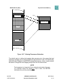
One way to avoid this situation is by disabling the chip-select region and enabling only
the dual-mapped region (DME = 1, but Vx = 0, where x = selected region, 0.3). Figure
10-17 illustrates the phenomena.
MPC555
USER’S MANUAL
MEMORY CONTROLLER
Revised 15 September 1999
MOTOROLA
10-22
MPC555 Memory Map
Dual Mapping
Physical External Memory
CSx
Dual-Map region
Flash
External CSx
Figure 10-17 Aliasing Phenomena Illustration
The default state is to allow dual-mapping data accesses only; this means that dual
mapping is possible only for data accesses on the internal bus. Also, the default state
takes the lower 2 Mbytes of the MPC555 internal flash memory. Hence, caution should
be taken to change the dual-mapping setup before the first data access.
NOTE
Dual mapping is not supported for an external master when the memory controller serves the access; In such a case, the MPC555
terminates the cycle by asserting TEA.
MPC555
USER’S MANUAL
MEMORY CONTROLLER
Revised 15 September 1999
MOTOROLA
10-23
10.7 Memory Controller External Master Support
The memory controller in the MPC555 supports accesses initiated by both internal and
external bus masters to external memories. If the address of any master is mapped
within the internal MPC555 address space, the access will be directed to the internal
device, and will be ignored by the memory controller. If the address is not mapped
internally, but rather mapped to one of the memory contoller regions, the memory controller will provide the appropriate chip select and strobes as programmed in the
corresponding region (see 6.13.1.3 External Master Control Register (EMCR).
The MPC555 supports only synchronous external bus masters. This means that the
external master works with CLKOUT and implements the MPC555 bus protocol to
access a slave device.
A synchronous master initiates a transfer by asserting TS. The ADDR[0:31] signals
must be stable from the rising edge of CLKOUT during which TS is sampled, until the
last TA acknowledges the transfer. Since the external master works synchronously
with the MPC555, only setup and hold times around the rising edge of CLKOUT are
important. Once the TS is detected/asserted, the memory controller compares the
address with each one of its defined valid banks to find a possible match. But, since
the external address space is shorter than the internal space, the actual addess that
is used for comparing against the memory controller regions is in the format of:
{00000000, bits 8:16 of the external address}. In the case where a match is found, the
controls to the memory devices are generated and the transfer acknowledge indication
(TA) is supplied to the master.
Since it takes two clocks for the external address to be recognized and handled by the
memory controller, the TS which is generated by the external master is ahead of the
corresponding CS and strobes which are asserted by the memory controller. This 2clock delay might cause problems in some synchronous memories. To overcome this,
the memory controller generates the MTS (memory transfer start) strobe which can be
used in the slave’s memory instead of the external master’s TS signal. As seen in Figure 10-18, the MTS strobe is synchronized to the assertion of CS by the memory
controller so that the external memory can latch the external master’s address correctly. To activate this feature, the MTSC bit must be set in the SIUMCR register. Refer
to 6.13.1.1 SIU Module Configuration Register for more information.
When the external master accesses the internal flash when it is disabled, then the
access is terminated with transfer error acknowledge (TEA pin) asserted, and the
memory controller does not support this access in any way.
When the memory controller serves an external master, the BDIP pin becomes an
input pin. This pin is watched by the memory controller to detect when the burst is
terminated.
MPC555
USER’S MANUAL
MEMORY CONTROLLER
Revised 15 September 1999
MOTOROLA
10-24
Synchronous External Master
TA
TS
BDIP
Data
ADDR
BURST
MPC555
Memory
TA
TS
MTS
TS
Address
Address
CSx
CE
OE
OE
WE/BE
W
BDIP
BDIP
Data
Data
BURST
BURST
Note that the memory controller’s BDIP line is used as a burst_in_progress signal.
Figure 10-18 Synchronous External Master
Configuration For GPCM–Handled Memory Devices
MPC555
USER’S MANUAL
MEMORY CONTROLLER
Revised 15 September 1999
MOTOROLA
10-25
Address
Match
&
Compare
Memory
Device
Access
CLOCK
ADDR[0:31]
RD/WR
BURST
TSIZE
TS
MTS
TA
CS
WE/BE
OE
Data
Figure 10-19 Synchronous External Master Basic Access (GPCM controlled)
Note that since the MPC555 has only 24 address pins, the eight most significant internal address lines are driven as 0x0000_0000, and so compared in the memory
controller’s regions.
MPC555
USER’S MANUAL
MEMORY CONTROLLER
Revised 15 September 1999
MOTOROLA
10-26
10.8 Programming Model
The following registers are used to control the memory controller.
Table 10-5 Memory Controller Address Map
Address
Register
0x2F C100
Base Register Bank 0 (BR0)
0x2F C104
Option Register Bank 0 (OR0)
0x2F C108
Base Register Bank 1 (BR1)
0x2F C10C
Option Register Bank 1 (OR1)
0x2F C110
Base Register Bank 2 (BR2)
0x2F C114
Option Register Bank 2 (OR2)
0x2F C118
Base Register Bank 3 (BR3)
0x2F C11C
Option Register Bank 3 (OR3)
0x2F C120 —
0x13F
Reserved
0x2F C140
Dual-Mapping Base Register (DMBR)
0x2F C144
Dual-Mapping Option Register (DMOR)
0x2F C148 —
0x2F C174
Reserved
0x2F C178
Memory Status Register (MSTAT)
Note:
In all subsequent registers bit tables, if two reset values are given: the upper is for CSx, x = 1, 2, 3, and the lower
is dedicated to CS0
10.8.1 General Memory Controller Programming Notes
1. In the case of an external master that accesses an internal MPC555 module (in
slave or peripheral mode), if that slave device address also matches one of the
memory controller’s regions, the memory controller will not issue any CS for this
access, nor will it terminate the cycle. Thus, this practice should be avoided. Be
aware also that any internal slave access prevents memory controller operation.
2. If the memory controller serves an external master, then it can support accesses to 32-bit port devices only. This is because the MPC555 external bus interface cannot initiate extra cycles to complete an access to a smaller port-size
device as it does not own the external bus.
3. When the SETA bit in the base register is set, then the timing programming for
the various strobes (CS, OE and WE/BE) may become meaningless.
MPC555
USER’S MANUAL
MEMORY CONTROLLER
Revised 15 September 1999
MOTOROLA
10-27
10.8.2 Memory Controller Status Registers (MSTAT)
,
MSTAT — Memory Controller Status Register
MSB
0
1
2
3
4
5
6
7
RESERVED
0x2F C178
8
9
10
11
12
WPER0WPER1WPER2WPER3
13
14
LSB
15
RESERVED
HARD RESET:
0
0
0
0
0
0
0
0
0
0
0
0
0
0
0
0
Table 10-6 MSTAT Bit Settings
Bit(s)
Name
0:7
—
8:11
Description
Reserved
Write protection error for bank x. This bit is asserted when a write-protect error occurs for the
WPER0 – associated memory bank. A bus monitor (responding to TEA assertion) will, if enabled, prompt
WPER3 the user to read this register if TA is not asserted during a write cycle. WPERx is cleared by writing one to the bit or by performing a system reset. Writing a zero has no effect on WPER.
12:15
—
Reserved
10.8.3 Memory Controller Base Registers (BR0 – BR3)
,
BR0 – BR3 — Memory Controller Base Registers 0 – 3 0x2F C100, C108, C110, C118
MSB
0
1
2
3
4
5
6
7
8
9
10
11
12
13
14
15
BA
HRESET
U
U
U
U
U
U
U
U
U
U
U
U
U
U
U
U
16
17
18
19
20
21
22
23
24
25
26
27
28
29
30
LSB
31
PS
RESERVED
WP
BI
V
ID[4:5]*
0
0
1
ID3**
BA
AT
RESERVED
WEBS TBDIP LBDIP SETA
HRESET
U
U
U
U
0
0
0
0
0
* Reset value is determined by the value on the internal data bus during reset.
** The BR0 Reset value is determined by the value on the internal data bus during reset (reset-configuration word). The
reset value of the V bit of BR1-3 = 0.
MPC555
USER’S MANUAL
MEMORY CONTROLLER
Revised 15 September 1999
MOTOROLA
10-28
Table 10-7 BR0 – BR3 Bit Settings
Bit(s)
Name
Description
BA
Base address. These bits are compared to the corresponding unmasked address signals among
ADDR[0:16] to determine if a memory bank controlled by the memory controller is being
accessed by an internal bus master. (The address types are also compared.) These bits are used
in conjunction with the AM[0:16] bits in the OR.
AT
Address type. This field can be used to require accesses of the memory bank to be limited to a
certain address space type. These bits are used in conjunction with the ATM bits in the OR. Note
that the address type field uses only AT[0:2] and does not need AT[3] to define the memory type
space. For a full definition of address types, refer to 9.5.7.6 Address Types.
20:21
PS
Port size
00 = 32-bit port
01 = 8-bit port
10 = 16-bit port
11 = Reserved
22
—
Reserved
0:16
17:19
Write protect. An attempt to write to the range of addresses specified in a base address register
that has this bit set can cause the TEA signal to be asserted by the bus-monitor logic (if enabled),
causing termination of this cycle.
0 = Both read and write accesses are allowed
1 = Only read accesses are allowed. The CSx signal and TA are not asserted by the memory
controller on write cycles to this memory bank. WPER is set in the MSTAT register if a write
to this memory bank is attempted
23
WP
24:25
—
26
WEBS
Write-enable/byte-select. This bit controls the functionality of the WE/BE pads.
0 = The WE/BE pads operate as WE
1 = The WE/BE pads operate as BE
27
TBDIP
Toggle-burst data in progress. TBDIP determines how long the BDIP strobe will be asserted for
each data beat in the burst cycles.
Reserved
Late-burst-data-in-progress (LBDIP). This bit determines the timing of the first assertion of the
BDIP pin in burst cycles.
28
29
30
LBDIP
SETA
BI
Note: it is not allowed to set both LBDIP and TBDIP bits in a region’s base registers; the behavior
of the design in such cases is unpredictable.
0 = Normal timing for BDIP assertion (asserts one clock after negation of TS
1 = Late timing for BDIP assertion (asserts after the programmed number of wait states
External transfer acknowledge
0 = TA generated internally by memory controller
1 = TA generated by external logic. Note that programming the timing of CS/WE/OE strobes may
have no meaning when this bit is set
Burst inhibit
0 = Memory controller drives BI negated (high). The bank supports burst accesses.
1 = Memory controller drives BI asserted (low). The bank does not support burst accesses.
Note: Following a system reset, the BI bit is set in OR0.
31
V
MPC555
USER’S MANUAL
Valid bit. When set, this bit indicates that the contents of the base-register and option-register
pair are valid. The CS signal does not assert until the V-bit is set. Note that an access to a region
that has no V-bit set may cause a bus monitor timeout. Note also that following a system reset,
the V-bit in BR0 reflects the value of ID3 in the reset configuration word.
MEMORY CONTROLLER
Revised 15 September 1999
MOTOROLA
10-29
10.8.4 Memory Controller Option Registers (OR0 – OR3)
,
OR0 – OR3 — Memory Controller Option Registers 0 – 3
MSB
0
1
2
3
4
5
6
7
0x2F C104, C10C,
C114, C11C
8
9
10
11
12
13
14
15
AM*
HRESET:
(OR[1:3])
U
U
U
U
U
U
U
U
U
U
U
U
U
U
U
U
HRESET
(OR0)
0
0
0
0
0
0
0
0
0
0
0
0
0
0
0
0
16
17
18
19
20
21
22
23
24
25
26
27
28
29
30
LSB
31
AM*
ATM
CSNT
ACS
EHTR
SCY
BSCY
TRLX
HRESET: (OR[1:3]):
U
U
U
U
U
U
U
U
U
U
U
U
U
U
U
U
0
0
0
0
0
0
1
1
1
1
0
1
1
0
HRESET
(OR0)
0
0
*It is recommended that this field would hold values that are the power of 2 minus 1 (e.g., - 23 - 1 = 7 [0b111]).
MPC555
USER’S MANUAL
MEMORY CONTROLLER
Revised 15 September 1999
MOTOROLA
10-30
Table 10-8 OR0 – OR3 Bit Settings
Bit(s)
0:16
Name
AM
Description
Address mask. This field allows masking of any corresponding bits in the associated base register. Masking the address bits independently allows external devices of different size address
ranges to be used. Any clear bit masks the corresponding address bit. Any set bit causes the
corresponding address bit to be used in comparison with the address pins. Address mask bits
can be set or cleared in any order in the field, allowing a resource to reside in more than one area
of the address map. This field can be read or written at anytime.
Following a system reset, the AM bits are reset in OR0.
17:19
ATM
Address type mask. This field masks selected address type bits, allowing more than one address
space type to be assigned to a chip-select. Any set bit causes the corresponding address type
code bits to be used as part of the address comparison. Any cleared bit masks the corresponding
address type code bit. Clear the ATM bits to ignore address type codes as part of the address
comparison. Note that the address type field uses only AT[0:2] and does not need AT[3] to define
the memory type space.
Following a system reset, the ATM bits are reset in OR0.
20
CSNT
Chip-select negation time. Following a system reset, the CSNT bit is reset in OR0.
0 = CS/WE are negated normally.
1 = CS/WE are negated a quarter of a clock earlier than normal
Following a system reset, the CSNT bit is reset in OR0.
21:22
ACS
Address to chip-select setup. Following a system reset, the ACS bist are reset in OR0.
00 = CS is asserted at the same time that the address lines are valid.
01 = Reserved
10 = CS is asserted a quarter of a clock after the address lines are valid.
11 = CS is asserted half a clock after the address lines are valid
Following a system reset, the ACS bits are reset in OR0.
23
EHTR
Extended hold time on read accesses. This bit, when asserted, inserts an idle clock cycle after a
read access from the current bank and any MPC555 write accesses or read accesses to a different bank.
0 = Memory controller generates normal timing
1 = Memory controller generates extended hold timing
Cycle length in clocks. This four-bit value represents the number of wait states inserted in the
single cycle, or in the first beat of a burst, when the GPCM handles the external memory access.
Values range from from 0 (0b0000) to 15 (0b1111). This is the main parameter for determining
the length of the cycle.
24:27
SCY
The total cycle length may vary depending on the settings of other timing attributes.
The total memory access length is (2 + SCY) x Clocks.
If the user has selected an external TA response for this memory bank (by setting the SETA bit),
then the SCY field is not used.
Note: Following a system reset, the SCY bits are set to 0b1111 in OR0.
MPC555
USER’S MANUAL
MEMORY CONTROLLER
Revised 15 September 1999
MOTOROLA
10-31
Table 10-8 OR0 – OR3 Bit Settings (Continued)
Bit(s)
Name
Description
Burst beats length in clocks. This field determines the number of wait states inserted in all burst
beats except the first, when the GPCM starts handling the external memory access and thus
using SCY[0:3] as the main parameter for determining the length of that cycle.
The total cycle length may vary depending on the settings of other timing attributes.
The total memory access length for the beat is is (1 + BSCY) x Clocks.
28:30
BSCY
31
TRLX
If the user has selected an external TA response for this memory bank (by setting the SETA bit)
then BSCY[0:3] are not used.
000 = 0-clock-cycle (1 clock per data beat)
001 = 1-clock-cycle wait states (2 clocks per data beat)
010 = 2-clock-cycle wait states (3 clocks per data beat)
011 = 3-clock-cycle wait states (4 clocks per data beat)
1xx = Reserved
Timing relaxed. This bit, when set, modifies the timing of the signals that control the memory
devices during a memory access to this memory region. Relaxed timing multiplies by two the
number of wait states determined by the SCY and BSCY fields. Refer to 10.3.5 Summary of
GPCM Timing Options for a full list of the effects of this bit on pins timing.
0 = Normal timing is generated by the GPCM.
1 = Relaxed timing is generated by the GPCM
Following a system reset, the TRLX bit is set in OR0.
10.8.5 Dual Mapping Base Register (DMBR)
,
DMBR — Dual Mapping Base Register
MSB
0
1
2
3
0
4
5
6
0x2F C140
7
BA
8
9
10
RESERVED
11
12
13
AT
14
15
RESERVED
HARD RESET:
0
U
U
U
U
U
U
0
0
0
0
0
1
0
0
0
16
17
18
19
20
21
22
23
24
25
26
27
28
29
30
LSB
31
RESERVED
DMCS
DME
HARD RESET:
0
0
0
0
0
0
0
0
0
0
0
0
0
0
0
ID31*
*The reset value is a reset configuration word value extracted from the indicated internal data bus lines.
MPC555
USER’S MANUAL
MEMORY CONTROLLER
Revised 15 September 1999
MOTOROLA
10-32
Table 10-9 DMBR Bit Settings
Bit(s)
Name
0
—
Reserved
BA
Base address. The base address field is compared (along with the address type field) to the
address of the address bus to determine whether an address should be dual-mapped by one
of the memory banks controlled by the memory controller. These bits are used in conjunction
with the AM[11:16] bits in the OR.
1:6
Description
Bit 10: is cleared at reset. That way, the default range for the dual mapping is 2 Mbyte. Note
that by setting this bit, the range becomes 4 Mbyte, which includes memory space beyond the
flash EEPROM memory.
7:9
—
Reserved
10:12
AT
Address type. This field can be used to specify that accesses involving the memory bank are
limited to a certain address space type. These bits are used in conjunction with the ATM bits
in the OR. The default value at reset is to map data only. For a full definition of address types,
refer to 9.5.7.6 Address Types.
13:27
—
Reserved
28:30
DMCS
31
DME
Dual-mapping chip select. This field determines which chip-select pin is assigned for dual
mapping.
000 = CS0
001 = CS1
010 = CS2
011 = CS3
1xx = Reserved
Dual mapping enabled. This bit indicates that the contents of the dual-mapping registers and
associated base and option registers are valid and enables the dual-mapping operation. The
default value at reset comes from the internal data bus that reflects the reset configuration
word. See 10.6 Dual Mapping of the Internal Flash EEPROM Array for more information.
0 = Dual mapping is not active
1 = Dual mapping is active
10.8.6 Dual-Mapping Option Register
,
DMOR — Dual-Mapping Option Register
MSB
0
1
2
3
0
4
AM
5
6
7
*
0x2F C144
8
9
10
RESERVED
11
12
13
ATM
14
15
RESERVED
RESET:
0
0
0
0
0
0
0
0
0
0
0
0
1
0
0
0
16
17
18
19
20
21
22
23
24
25
26
27
28
29
30
LSB
31
0
0
0
0
0
0
0
RESERVED
RESET:
0
0
0
0
0
0
0
0
0
*It is recommended that this field would hold values that are the power of 2 minus 1 (e.g., - 23 - 1 = 7 [0b111]).
MPC555
USER’S MANUAL
MEMORY CONTROLLER
Revised 15 September 1999
MOTOROLA
10-33
Table 10-10 DMOR Bit Settings
Bit(s)
Name
Description
0
—
Reserved
1:6
AM
Address mask. The address mask field of each option register provides for masking any of the
corresponding bits in the associated base register. By masking the address bits independently, external devices of different size address ranges can be used. Any clear bit masks the
corresponding address bit. Any set causes the corresponding address bit to be used in the
comparison with the address pins. Address mask bits can be set or cleared in any order in the
field, allowing a resource to reside in more than one area of the address map. This field can
be read or written at any time.
7:9
—
Reserved
Address type mask. This field can be used to mask certain address type bits, allowing more
than one address space type to be assigned to a chip select. Any set bit causes the corresponding address type code bits to be used as part of the address comparison. Any cleared
bit masks the corresponding address type code bit.
10:12
ATM
To instruct the memory controller to ignore address type codes as part of the address comparison, clear the ATM bits.
Note: Following a system reset, the ATM bits are cleared in DMOR, except the ATM2 bit. This
means that only data accesses are dual mapped. Refer to the address types definition in Table
9-8.
13:31
—
MPC555
USER’S MANUAL
Reserved
MEMORY CONTROLLER
Revised 15 September 1999
MOTOROLA
10-34