1
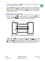
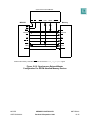
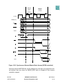
To support different types of memory devices, the memory controller supports two
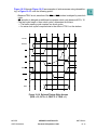
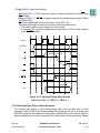
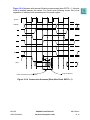
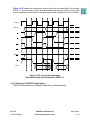
types of timing for the BDIP signal: normal and late. Note that the BDIP pin itself is controlled by the external bus interface logic. Refer to Figure 9-13 and Figure 9-14 in
SECTION 9 EXTERNAL BUS INTERFACE.
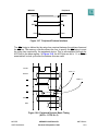
If the memory controller is used to support an external master accessing an external
device with bursts, the BDIP input pin is used to indicate to the memory controller
when the burst is terminated.
For addition details, refer to 9.5.3 Burst Transfer.
10.3 Chip-Select Timing
The GPCM allows a glueless and flexible interface between the MPC555 and SRAM,
EPROM, EEPROM, ROM devices and external peripherals. When an address and
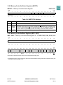
address type matches the values programmed in the BR and OR for one of the memory controller banks, the attributes for the memory cycle are taken from the OR and
BR registers as well. These attributes include the following fields: CSNT, ACS, SCY,
BSCY, WP, TRLX, BI, PS, and SETA.
Byte write and read-enable signals (WE/BE(0:3)) are available for each byte that is
written to or read from memory. An output enable (OE) signal is provided to eliminate
external glue logic for read cycles. Upon system reset, a global (boot) chip select is
available. This provides a boot ROM chip select before the system is fully configured.
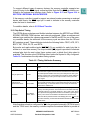
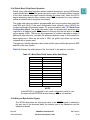
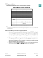
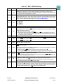
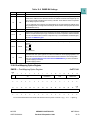
Table 10-1 summarizes the chip-select timing options.
Table 10-1 Timing Attributes Summary
Timing Attribute
Access speed
Intercycle space time
Synchronous or
asynchronous device
Wait states
Bits/Fields
Description
TRLX
The TRLX (timing relaxed) bit determines strobe timing to be fast or relaxed.
EHTR
The EHTR (extended hold time on read accesses) bit is provided for devices that have long disconnect times from the data bus on read accesses. EHTR specifies whether the next cycle is delayed one clock cycle
following a read cycle, to avoid data bus contentions. EHTR applies to
all cycles following a read cycle except for another read cycle to the
same region.
ACS, CSNT
The ACS (address-to-chip-select setup) and CSNT (chip-select negation time) bits cause the timing of the strobes to be the same as the address bus timing, or cause the strobes to have setup and hold times
relative to the address bus.
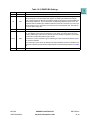
SCY, BSCY,
SETA, TRLX
From zero to 15 wait states can be programmed for any cycle that the
memory controller generates. The transfer is then terminated internally.
In simplest case, the cycle length equals (2 + SCY) clock cycles, where
SCY represents the programmed number of wait states (cycle length in
clocks). The number of wait states is doubled if the TRLX bit is set.
When the SETA (external transfer acknowledge) bit is set, TA must be
generated externally, so that external hardware determines the number
of wait states.
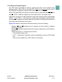
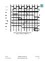
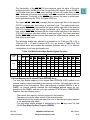
Note that when a bank is configured for TA to be generated externally (SETA bit is set)
and the TRLX is set, the memory controller requires the external device to provide at
MPC555
USER’S MANUAL
MEMORY CONTROLLER
Revised 15 September 1999
MOTOROLA
10-6