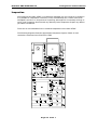
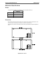
1
BQTcd_^U@=31D=6=Q^eQ\ 9cceU! @eR\YSQdY_^>_@=31D=6 88 © Radstone Technology PLC 1997. All rights reserved. This publication is issued to provide outline information only which (unless agreed by the Company in writing) may not be used, applied or reproduced for any purpose or form part of any order or contract or be regarded as a representation relating to products or services concerned. The Company reserves the right to alter without notice the specification, design, price or conditions of supply of any product or service. >_fU]RUb!))' 6b_^dY9cceU! DbQTU]Qb[c Radstone and the Radstone symbol are trademarks of Radstone Technology PLC. All other company and product names are acknowledged as being the trademarks or registered trademarks of their respective companies. 4_Se]U^d8Ycd_bi Issue 1 Date 11/97 2 3 4 5 6 9]`_bdQ^d For future reference, please record your PMC-ATMF’s serial, MIC and IP numbers. 6b_^dYY9cceU! BQTcd_^U@=31D=6=Q^eQ\ 3_^dU^dc 3XQ`dUb!9^db_TeSdY_^ Documentation Objectives .......................................................................................................1-2 Documentation Audience .........................................................................................................1-2 Documentation Scope ...............................................................................................................1-2 Documentation Structure ........................................................................................................1-3 Warnings ...................................................................................................................................1-4 Documentation Conventions....................................................................................................1-5 Related Documents...................................................................................................................1-6 World Wide Web Sites..............................................................................................................1-6 3XQ`dUb"7U^UbQ\4UcSbY`dY_^ Features ....................................................................................................................................2-1 Functional Overview ................................................................................................................2-3 Software Support......................................................................................................................2-3 Mechanical Overview ...............................................................................................................2-4 Level 1/Standard (S-style) .............................................................................................2-4 Level 2/Extended Temperature (X-style)......................................................................2-4 Level 3/Rugged Air-cooled (RA-style) ...........................................................................2-5 Level 4/Rugged Conduction-cooled (RC-style)..............................................................2-5 3XQ`dUb#E^`QS[Y^WQ^T9^c`USdY_^ Unpacking .................................................................................................................................3-1 Board Identification .................................................................................................................3-1 Inspection..................................................................................................................................3-2 3XQ`dUb$3_^^USd_bc P11 and P12 Pinouts ................................................................................................................4-2 3XQ`dUb%3_^VYWebQdY_^Q^T9^cdQ\\QdY_^ Configuration............................................................................................................................5-1 Installation................................................................................................................................5-1 3_^dU^dcY9cceU! Radstone PMC-ATMF Manual Chapter 6 - Functional Description PCI Interface.............................................................................................................................................6-1 PCI Commands.........................................................................................................................................6-1 Configuration Space .................................................................................................................................6-2 Vendor ID Register .......................................................................................................................6-2 Device ID Register ........................................................................................................................6-2 Command Register ........................................................................................................................6-3 Status Register...............................................................................................................................6-4 PCI Configuration Register 1 ........................................................................................................6-5 PCI Configuration Register 2 ........................................................................................................6-5 I/O Base Address Register ............................................................................................................6-6 Memory Base Address Register ....................................................................................................6-6 Expansion ROM Base Address Register .......................................................................................6-6 Bus Grant and Interrupt Register...................................................................................................6-7 NICStAR Network Operation Device.......................................................................................................6-8 Data Register 0 to Data Register 3 ................................................................................................6-9 Command Register ......................................................................................................................6-10 Configuration Register ................................................................................................................6-16 Status Register.............................................................................................................................6-20 Receive Status Queue Base Register ...........................................................................................6-22 Receive Status Queue Tail Register ............................................................................................6-23 Receive Status Queue Head Register ..........................................................................................6-24 Cell Drop Count Register ............................................................................................................6-25 VPI/VCI Lookup Error Count Register.......................................................................................6-26 Invalid Cell Count Register .........................................................................................................6-27 Raw Cell Tail Register ................................................................................................................6-27 Timer Register.............................................................................................................................6-27 Transmit Schedule Table Base Register......................................................................................6-27 Transmit Status Queue Base Register..........................................................................................6-28 Transmit Status Queue Tail Register...........................................................................................6-28 Transmit Status Queue Head Register.........................................................................................6-29 General Purpose Register ............................................................................................................6-30 VPI/VCI Mask Register ..............................................................................................................6-31 Local SRAM Memory Map....................................................................................................................6-32 EEPROM................................................................................................................................................6-33 Flash .......................................................................................................................................................6-33 LEDs.......................................................................................................................................................6-33 Chapter 7 - Troubleshooting Appendix A - Specifications General .................................................................................................................................................... A-1 Electrical.................................................................................................................................................. A-2 Environmental Specifications .................................................................................................................. A-3 Mechanical Specifications ....................................................................................................................... A-4 Reliability ................................................................................................................................................ A-5 Ordering Information............................................................................................................................... A-5 Glossary Index Page (ii) Issue 1 9^db_TeSdY_^ BQTcd_^U@=31D=6=Q^eQ\ 3XQ`dUb!9^db_TeSdY_^ Radstone’s PMC-ATMF is a 155 Mbits/sec ATM adapter for use in OC-3 fiber networks. PMC-based, the PMC-ATMF is a fourth-generation adapter that has been developed to address the need for reliable, high performance ATM in embedded systems. Applications for the PMC-ATMF range from low cost LANs, through enterprise level ATM backbones, to edge devices for WANs providing added value services. The PMC-ATMF forms part of an expansion board range complementing Radstone’s latest generation of PMC compatible, PowerPC-based single board processors, adding industry-leading price/performance ATM functionality in a single VME slot. Like all Radstone’s VME products, the PMC-ATMF is available in a compatible range of increasingly more rugged build styles. In this case Level 1 (Standard), suitable for a benign office-like environment, right through to Level 4 (Rugged Conduction Cooled), capable of withstanding the harshest of environments. All products are COTS/NDI, and make maximum use of low cost plastic packaged integrated circuits to ensure the most cost effective solution, whatever the market. In its air-cooled build levels, the PMC-ATMF conform with the IEEE P1386.1 PMC standard, and in the conduction-cooled build level, it conforms with the latest Draft standard for Conduction Cooled PMCs. Radstone is a key member of the VITA standards committee, setting the standards for rugged conduction-cooled PMCs. On build levels 1 and 2, fiber optic connections are made using an industry standard SC connector through the front panel. On level 3 and 4 build standards, the fiber optic cable is provided in a pig-tailed assembly. The PMC-ATMF’s form factor (approximately 149 x 74 mm) uses only one PMC slot on the host and can easily be plugged onto any host processor (VME or otherwise) that supports PMC and has appropriate drivers, for example, Radstone’s PPC1, PPC1A or the rugged PPC2. @QWU!!9cceU! BQTcd_^U@=31D=6=Q^eQ\ 9^db_TeSdY_^ 4_Se]U^dQdY_^?RZUSdYfUc This manual provides the user with sufficient information to configure, install and use the Radstone PMC-ATMF expansion board. 4_Se]U^dQdY_^1eTYU^SU This manual is written to cover, as far as possible, the range of people who will handle or use the PMC-ATMF, from unpackers/inspectors, through system managers and installation technicians to hardware and software engineers. Most chapters assume a certain amount of knowledge on the subjects of single board computer architecture, interfaces, peripherals, systems, cabling, grounding and PCI. There is a glossary provided at the back of this manual that explains some of the terms used and expands all abbreviations. 4_Se]U^dQdY_^CS_`U This manual describes all variants and build standards of the PMC-ATMF. Application software, operating systems and drivers are described in separate manuals. The Radstone host processor is also described in a separate manual. @QWU!"9cceU! 9^db_TeSdY_^ BQTcd_^U@=31D=6=Q^eQ\ 4_Se]U^dQdY_^CdbeSdebU This manual is structured in a way that will reflect the sequence of operations from receipt of the PMC-ATMF up to getting it working with your host processor. Each topic is covered in a separate chapter and each chapter begins with a brief introduction that tells you what the chapter contains. In this way, you can skip any chapters that are not applicable or with which you are already familiar. The chapters are: Chapter 1 (this chapter) - gives a brief introduction, this manual's objectives, audience and scope, the structure, some warnings, conventions and related documentation. Chapter 2 - is a slightly more detailed, but still general product description. Chapter 3 - contains unpacking and inspection instructions. Chapter 4 - describes the PMC-ATMF’s connectors and signals used. Chapter 5 - describes fitting the module to a host. Chapter 6 - is a functional description. Chapter 7 - gives troubleshooting guidelines. Appendix A - is a board specification. There are also a glossary and an index provided. @QWU!#9cceU! BQTcd_^U@=31D=6=Q^eQ\ 9^db_TeSdY_^ GQb^Y^Wc Do not exceed the maximum rated input voltages or apply reversed bias to the assembly. If such conditions occur, toxic fumes may be produced due to the destruction of components. @QWU!$9cceU! 9^db_TeSdY_^ BQTcd_^U@=31D=6=Q^eQ\ 4_Se]U^dQdY_^3_^fU^dY_^c All numbers are expressed in decimal, except addresses and memory or register data, which are expressed in hexadecimal. Where confusion may occur, decimal numbers have a ‘D’ subscript and binary numbers have a ‘B’ subscript. The prefix ‘0x’ shows a hexadecimal number, following the ‘C’ programming language convention. Information of particular importance is highlighted by `Note:’. The multipliers ‘k’, ‘M’ and ‘G’ have their conventional scientific and engineering meanings of *103, *106 and *109 respectively. The only exception to this is in the description of the size of memory areas, when ‘K’, ‘M’ and ‘G’ mean *2 10, *220 and *230 respectively. When describing transfer rates, ‘k’ ‘M’ and ‘G’ mean *103, *106 and *109 not *210 *220 and *230. Bits are numbered from 0 to n, where 0 is the LSB and n is the MSB. Signal names follow the IEEE P1386.1. Signal names ending with a tilde (~) denote active low signals; all other signals are active high. PCI (PMC) is a little-endian environment, i.e. data is stored with the least significant byte at the lowest address. @QWU!%9cceU! BQTcd_^U@=31D=6=Q^eQ\ 9^db_TeSdY_^ BU\QdUT4_Se]U^dc • IEEE P1386.1, Draft Standard Physical and Environmental Layers for PCI Mezzanine Cards: PMC, Draft 2.0 4-Apr-95 • IEEE P1386, Draft Standard for a Common Mezzanine Card Family: CMC, Draft 2.0 4-Apr-95 • Draft Standard for Conduction-cooled PMC Modules • PCI Local Bus Specification, Revision 2.1 1-Jun-95 • IDT77211 NICStAR User Manual, Version 1.0 26-Feb-97 • Radstone PPC1-60x Manual, publication number RT26358 • Radstone PPC1A-60x Manual, publication number PPC1A-0HH • Radstone PPC2-60x Manual, publication number RT5070 G_b\TGYTUGURCYdUc Radstone on the world-wide-web is available at: http://www.radstone.co.uk or http://www.radstone.com @QWU!&9cceU! 7U^UbQ\4UcSbY`dY_^ BQTcd_^U@=31D=6=Q^eQ\ 3XQ`dUb"7U^UbQ\4UcSbY`dY_^ This chapter contains a general description of the PMC-ATMF. Chapter 6 describes the board in more detail. The PMC-ATMF provides a 32-bit PCI interface, and fibre optic connections are made using an SC connection on the front panel on build levels 1 and 2 and as a pig-tailed assembly on build levels 3 and 4. 6UQdebUc • Complete 155 Mbps ATM network interface card • Multimode fiber optical interface • Supports up to 16,384 receive connections • Supports more than 20,000 transmit connections • Serial EEPROM for system information storage • Optional Flash device for BIT/BIST code storage • Build options: Level 1 (S), Level 2 (X), Level 3 (RA) and Level 4 (RC) • VxWorks driver from End to End Systems • SC connectors on build levels 1 to 3 • MIL-T-29504/14 terminated fiber pig-tails on build level 4 • 32-bit, 33 MHz PCI 2.1 interface • 32-bit scatter-gather DMA support • Highly integrated design • Single slot PMC IEEE P1386 form factor • ForeThought 4 ATM internetworking software for Tornado • UNI 3.0/3.1 SVCs @QWU"!9cceU! 7U^UbQ\4UcSbY`dY_^ BQTcd_^U@=31D=6=Q^eQ\ 6YWebU"!@=31D=62\_S[4YQWbQ] @QWU""9cceU! 7U^UbQ\4UcSbY`dY_^ BQTcd_^U@=31D=6=Q^eQ\ 6e^SdY_^Q\?fUbfYUg The highly integrated design of the PMC-ATMF comprises a 32-bit, 33 MHz PCI 2.1 compliant NIC with on-board SAR and PCI bus support, and 128 Kbytes of on-board buffer RAM. The PMC-ATMF supports 32-bit burst mode, bus master scatter-gather DMA and block transfers up to 12 words to achieve unprecedented performance levels. AAL0, AAL 3/4 and AAL 5 are supported on hardware, as are ‘Raw Cell’ formats. ATM cell processing conforms to ANSI T1S1 5/92-002R3, ITU I.361 and the ATM Forum UNI 3.0/3.1 specifications. 1bSXYdUSdebU The PMC-ATMF is based on the NICStAR, which has a 33 MHz PCI 2.1 compliant bus interface that supports bus master DMA. ATM SAR functions are provided, together with support for 128 Kbytes of buffer RAM. PHY functions are contained in the PM5346. OC-3 connectivity is contained within the SC connectors for levels 1 and 2, and by custom designed optical circuits for levels 3 and 4. 6YRUbQ^T3_^^USd_bc The PMC-ATMF is designed to operate with duplex 62.5/125µ multimode fiber (2,000 metres maximum, 10 dB loss). Connection to the PMC-ATMF in build levels 1 and 2 is by an industry standard SC optical connector. Build levels 3 and 4 are delivered with 1.5 m pig-tail connectors terminated with MIL-T-29504/14 multimode long pin termini. Field proven, these are suitable for use with MIL-C-28876 connectors for Naval applications, and MIL-C-38999 connectors for avionics, shipboard or ground deployment. @UbV_b]Q^SU Capable of transmitting over 11,000 512 byte UDP packets per second when used with a Radstone PowerPC 603 CPU, the PMC-ATMF brings new levels of performance to embedded ATM solutions. With larger messages the full ATM line rate is virtually sustained (149 Mbits per second). These performance levels represent a fivefold performance increase over existing embedded ATM products. C_VdgQbUCe``_bd ForeThought 4 ATM Internetworking Software is available for the PMC-ATMF. Developed by industry leader FORE Systems, ForeThought 4 is a layered software solution that provides high-performance, scaleable networking services for applications in both LAN and WAN environments. Radstone Technology, as a FORE development partner, has ported ForeThought 4 to VxWorks 5.3/Tornado, bringing unparalleled levels of networking application development and support to real-time embedded systems. ForeThought 4 from FORE is today’s leading ATM internetworking software. Licensed by over 140 of FORE’s vendors and partners, it has become the industry de-facto standard, and wide deployment of ForeThought 4 solutions mean that the developer is assured that their system will integrate seamlessly onto the network. ForeThought 4 presents a layered architecture to the programmer that allows the development of networking services that take advantage of the benefits of ATM in LAN and WAN environments. @QWU"#9cceU! 7U^UbQ\4UcSbY`dY_^ BQTcd_^U@=31D=6=Q^eQ\ =USXQ^YSQ\?fUbfYUg PMC cards use both single and double sided component mounting, depending on the product. Where the application requires only a single side, larger components, e.g. PGA devices or DIL packages are used. For more complex applications that require greater board space, surface mount devices are used, allowing components to be mounted on both sides of the board, yet still keep within the specified profile. The PMC-ATMF is available in four electrically compatible build styles. Each style is carefully tailored to a particular set of requirements and environments. All four styles fully support the power and versatility of PMC, so no matter how large or diversified your project, absolute compatibility is assured at all stages of development. The four build styles have two basic mechanical configurations: convection-cooled in accordance with IEEE P1386, and conduction-cooled in accordance with the proposed CCPMC standard being prepared by VITA. Convection-cooled boards include: Standard Extended Temperature Rugged Air-Cooled - PMCATMF-100 (Level 1) - PMCATMF-200 (Level 2) - PMCATMFR-300 (Level 3) Conduction-cooled boards include: Rugged Conduction-cooled - PMCATMF-400 (Level 4) A brief description of each build style follows. See the Environmental Specifications section in Appendix A for more details. <UfU\!CdQ^TQbTCcdi\U Intended for use in benign environments, the S-style also provides the ideal cost effective method of complete system development. The S-style assembly comprises IEEE P1386 size assembly with high quality commercial grade (plastic encapsulated) components. As software compatibility throughout the build styles is absolute, a system intended for final implementation in a severe tactical environment can be developed and debugged at low cost, switching over to the target style only in the final stages of system integration. <UfU\"5hdU^TUTDU]`UbQdebUHcdi\U As S-style, but conformally coated and 100% tested in manufacture to provide an extended operating range. @QWU"$9cceU! 7U^UbQ\4UcSbY`dY_^ BQTcd_^U@=31D=6=Q^eQ\ <UfU\#BeWWUT1YbS__\UTB1cdi\U RA-style boards are intended for applications that have extended temperature, shock and vibration requirements, but can be served by conventional, forced-air cooled, racking systems. These rugged boards comprise IEEE P1386 size assembly fitted with wide temperature range, industrial grade components and are conformally coated as standard. <UfU\$BeWWUT3_^TeSdY_^S__\UTB3cdi\U Designed primarily for use in sealed ATR chassis and other conduction-cooled environments the RC-style board features wide temperature range, industrial grade devices, an integral thermal management layer and incorporates a central stiffening bar for additional strength. Cooling is achieved through conduction of heat from the thermal management layer to the cold wall of the rack to which the boards are secured by screw driven wedgelocks. RC-style boards are 100% temperature characterised and conformally coated during manufacture. RC-style is mechanically compliant with the proposed CCPMC standard. @QWU"%9cceU! 3_^VYWebQdY_^Q^T9^cdQ\\QdY_^ BQTcd_^U@=31D=6=Q^eQ\ 3XQ`dUb#E^`QS[Y^WQ^T9^c`USdY_^ This chapter gives guidelines on unpacking and inspecting the PMC-ATMF. E^`QS[Y^W Radstone boards are protected by an antistatic envelope. Observe antistatic precautions and work at an approved antistatic work station when unpacking the board. The PMC-ATMF is shipped in an individual, reusable shipping box. When you receive the shipping container, inspect it for any evidence of physical damage. If the container is damaged, request that the carrier's agent is present when the carton is opened. Keep the contents and packing materials for the agent's inspection and notify Radstone's customer service department of the incident. Retain the packing list for reference. Assuming that there is no obvious damage, you may still want to keep the shipping carton in case you want to ship the PMC-ATMF on elsewhere. 2_QbT9TU^dYVYSQdY_^ The PMC-ATMF has labels attached to the solder side of the PCB (i.e. the side of the PCB visible when the PMC-ATMF is fitted to the host). These labels give the revision state (e.g. Rev A) and the module’s serial number. These are also given in bar-code form. @QWU#!9cceU! BQTcd_^U@=31D=6=Q^eQ\ 3_^VYWebQdY_^Q^T9^cdQ\\QdY_^ 9^c`USdY_^ Assuming that the PMC-ATMF is not obviously damaged, you can now go on to inspect it. It is possible for components (connectors, links, socketed chips etc.) to work loose or be dislodged in transit or in the process of unpacking, although this is extremely unlikely. A quick visual inspection should reveal any obviously loose components. Report any defects you detect to Radstone. There are no user-selectable links or socketed components on the PMC-ATMF. The following diagram shows the approximate component layouts of both air and conduction-cooled versions of the PMC-ATMF. @QWU#"9cceU! 3_^^USd_bc BQTcd_^U@=31D=6=Q^eQ\ 3XQ`dUb$3_^^USd_bc The PMC-ATMF connects directly to the host through two connectors designated P11 and P12. These connectors contain signals for the 32-bit PCI bus. 6YWebU$!3_^^USd_b@_cYdY_^c @QWU$!9cceU! BQTcd_^U@=31D=6=Q^eQ\ 3_^^USd_bc @!!Q^T@!"@Y^_edc P11 32-bit PCI P12 32-bit PCI Pin Signal Name Signal Name Pin Pin Signal Name Signal Name Pin 1 TCK -12V 2 1 +12V TRST~ 2 3 Ground INTA~ 4 3 TMS TDO 4 5 INTB~ INTC~ 6 5 TDI Ground 6 7 BUSMODE1~ +5V 8 7 Ground PCI-RSVD 8 9 INTD~ PCI-RSVD 10 9 PCI-RSVD PCI-RSVD 10 11 Ground PCI-RSVD 12 11 BUSMODE2~ +3.3V 12 13 CLK Ground 14 13 RST~ BUSMODE3~ 14 15 Ground GNT~ 16 15 +3.3V BUSMODE4~ 16 17 REQ~ +5V 18 17 PCI-RSVD Ground 18 19 V (I/O) AD[31] 20 19 AD[30] AD[29] 20 21 AD[28] AD[27] 22 21 Ground AD[26] 22 23 AD[25] Ground 24 23 AD[24] +3.3V 24 25 Ground C/BE3~ 26 25 IDSEL AD[23] 26 27 AD[22] AD[21] 28 27 +3.3V AD[20] 28 29 AD[19] +5V 30 29 AD[18] Ground 30 31 V (I/O) AD[17] 32 31 AD[16] C/BE[2]~ 32 33 FRAME~ Ground 34 33 Ground PMC-RSVD 34 35 Ground IRDY~ 36 35 TRDY~ +3.3V 36 37 DEVSEL~ +5V 38 37 Ground STOP~ 38 39 Ground LOCK~ 40 39 PERR~ Ground 40 41 SDONE~ SBO~ 42 41 +3.3V SERR~ 42 43 PAR Ground 44 43 C/BE[1]~ Ground 44 45 V (I/O) AD[15] 46 45 AD[14] AD[13] 46 47 AD[12] AD[11] 48 47 Ground AD[10] 48 49 AD[09] +5V 50 49 AD[08] +3.3V 50 51 Ground C/BE~ 52 51 AD[07] PMC-RSVD 52 53 AD[06] AD[05] 54 53 +3.3V PMC-RSVD 54 55 AD[04] Ground 56 55 PMC-RSVD Ground 56 57 V (I/O) AD[03] 58 57 PMC-RSVD PMC-RSVD 58 59 AD[02] AD[01] 60 59 Ground PMC-RSVD 60 61 AD[00] +5V 62 61 ACK64~ +3.3V 62 63 Ground REQ64~ 64 63 Ground PMC-RSVD 64 @QWU$"9cceU! 3_^VYWebQdY_^Q^T9^cdQ\\QdY_^ BQTcd_^U@=31D=6=Q^eQ\ 3XQ`dUb%3_^VYWebQdY_^Q^T9^cdQ\\QdY_^ This chapter describes the configuration of the PMC-ATMF and its connection to a PowerPC-based host board, e.g. Radstone’s PPC1 or PPC2. 3_^VYWebQdY_^ There are no user configurable links on the PMC-ATMF. All configuration is defined via software. 9^cdQ\\QdY_^ The connection of the PMC-ATMF to an air-cooled PowerPC host board (e.g. the PPC1) conforms to the IEEE P1386.1 standard. To connect the PMC-ATMF to an air-cooled host: 1. Before connection, check that the stand-offs are in position on the PMC-ATMF module. 2. Remove the PMC slot filler from the host’s front panel in the position where you want the PMC-ATMF to go. 3. Pass the bezel (front panel) of the PMC-ATMF through the vacant PMC slot opening in the host’s front panel. Press the PMC-ATMF’s connectors into the corresponding connectors on the host. Refer to Figure 5.1 overleaf. 4. When the PMC-ATMF board is correctly positioned, secure it to the host board using the supplied screws into the stand-offs. Connection to the PMC-ATMF in build levels 1 and 2 is by an industry standard SC optical connector. @QWU%!9cceU! BQTcd_^U@=31D=6=Q^eQ\ 3_^VYWebQdY_^Q^T9^cdQ\\QdY_^ The connection of the PMC-ATMF to a conduction-cooled PowerPC host board (e.g. the PPC2-604RC) conforms with the Draft Standard for Conduction Cooled PMCs, and is similar to the procedure for connection to an air-cooled host. To connect the PMC-ATMF to a conduction-cooled host: 1. Before connection, check that the stand-offs are in position on the PMC-ATMF module. 2. As there is no bezel (front panel) on the conduction-cooled PMC-ATMF, simply press the PMC-ATMF’s connectors into the corresponding connectors on the host. Refer to Figure 5.2. 3. When the PMC-ATMF board is correctly positioned, secure it to the host board using the screws supplied in the fixing kit into the stand-offs, and the tapped holes in the central and front panel stiffening bars. Metal to metal connections at the two stiffening points provide the heat transfer points for the conduction cooling. You are recommended to secure the screws into the tapped holes with a fixative such as Loctite-242 (Nutlock). 4. The PMC-ATMF fibers must be carefully attached at suitable points within the enclosure. Failure to do so may cause damage to the fiber and eventual failure of the module. Build levels 3 and 4 are delivered with 1.5 m pig-tail connectors terminated with MIL-T-29504/14 multimode long pin termini. Field proven, these are suitable for use with MIL-C-28876 connectors for Naval applications, and MIL-C-38999 connectors for avionics, shipboard or ground deployment. @QWU%"9cceU! 3_^VYWebQdY_^Q^T9^cdQ\\QdY_^ BQTcd_^U@=31D=6=Q^eQ\ 6YWebU%!@=31D=63_^^USdY_^d_1YbS__\UT8_cd @QWU%#9cceU! BQTcd_^U@=31D=6=Q^eQ\ 3_^VYWebQdY_^Q^T9^cdQ\\QdY_^ 6YWebU%"@=31D=63_^^USdY_^d_3_^TeSdY_^S__\UT8_cd Drawing - TBD @QWU%$9cceU! 6e^SdY_^Q\4UcSbY`dY_^ BQTcd_^U@=31D=6=Q^eQ\ 3XQ`dUb&6e^SdY_^Q\4UcSbY`dY_^ This chapter gives a functional description of the PMC-ATMF. @399^dUbVQSU The PMC-ATMF’s PCI interface is compliant with the PCI local bus specification. The interface uses the IDT77201/77211 NICStAR chip set. All data alignment in this manual refers to the PCI bus. How data appears to the processor depends entirely on the configuration of the host card and whether it is big- or little-endian. @393_]]Q^Tc PMC-ATMF responds to the following PCI bus commands: • Memory Read • Memory Write • Configuration Read • Configuration Write • Memory Read Multiple (aliased to Memory Read) • Memory Read Line (aliased to Memory Read) • Memory Write and Invalidate (aliased to Memory Write) @QWU&!9cceU! BQTcd_^U@=31D=6=Q^eQ\ 6e^SdY_^Q\4UcSbY`dY_^ 3_^VYWebQdY_^C`QSU The following table shows the PCI Configuration Register space. Shaded areas are not used and return 0 when accessed. 31 16 15 0 0x00 Device ID Register Vendor ID Register 0x04 Status Register Command Register 0x08 PCI Configuration Register 1 0x0C PCI Configuration Register 2 0x10 I/O Base Address Register 0x14 Memory Base Address Register 0x18 Reserved 0x1C Reserved 0x20 Reserved 0x24 Reserved 0x28 Reserved 0x2C Reserved 0x30 Expansion ROM Base Address Register 0x34 Reserved 0x38 Reserved 0x3C Bus Grant and Interrupt Register 0x40 Reserved 0xFC FU^T_b94BUWYcdUb This holds the value 0x111D, indicating IDT. 4UfYSU94BUWYcdUb This holds the value 0x0001, indicating a NICStAR. @QWU&"9cceU! 6e^SdY_^Q\4UcSbY`dY_^ BQTcd_^U@=31D=6=Q^eQ\ 3_]]Q^TBUWYcdUb This has the following layout: Bits Mnemonic 0 IOEN Description I/O access to NICStAR Enable. The default is 0. 0 = NICStAR does not respond to PCI bus I/O access. 1 = NICStAR does respond to PCI bus I/O access. 1 MEMEN Memory access to NICStAR Enable. The default is 0. 0 = NICStAR does not respond to PCI bus memory access. 1 = NICStAR does respond to PCI bus memory access. 2 MSTEN NICStAR Master Enable. The default is 0. 0 = NICStAR cannot generate master cycles. 1 = NICStAR can generate master cycles. 3 to 5 Reserved 6 PARDE Read as 0. Parity error Detect Enable. The default is 0. 0 = Ignore any parity error and continue normal operation (the parity error signal is still generated). 1 = Take action when a parity error is detected. 7 Reserved 8 SERRE Reads as 0. SERR~ pin Enable. The default is 0. 0 = SERR~ pin driver is disabled. 1 = SERR~ pin driver is enabled. 9 FSCYS Fast back-to-back host Cycle. The default is 0. 0 = Fast back-to-back transfers are allowed to the same agent when the NICStAR is a bus master. 1 = Fast back-to-back transfers are allowed to different agents when the NICStAR is a bus master. 10 to 15 Reserved Read as 0. @QWU	cceU! BQTcd_^U@=31D=6=Q^eQ\ 6e^SdY_^Q\4UcSbY`dY_^ CdQdecBUWYcdUb This has the following layout: Bits Mnemonic 16 to 22 Reserved 23 FSACC Description Read as 0. Fast back-to-back Access. Always reads as 1. This read-only bit indicates to the host that the NICStAR, as a target, can accept fast back-to-back bus transactions when they are not to the NICStAR. 24 PARED Parity Error Detected. The default is 0. 0 = No parity error detected. 1 = Both of the following conditions have occurred: a) NICStAR is bus master and PERR~ is asserted by the NICStAR or the target. b) The parity error response bit (bit 6 of the Control Register) is set. 25 and 26 IOSPD I/O access decode Speed These bits specify how fast the NICStAR can assert a DEVSEL~ signal in a target operation. These bits are read only, and always read as 01 for medium decode time (one wait state). 27 Reserved 28 TGABT Reads as 0. Target Abort. The default is 0. 0 = NICStAR Master bus cycles are not aborted by a target device. 1 = NICStAR Master bus cycles are aborted due to target aborting. This bit is cleared by writing a 1 to it. 29 MRABT Master Abort. The default is 0. 0 = NICStAR Master bus cycles were completed successfully. 1 = DEVSEL~ signal from target was not activated after seven PCI clocks. This bit is cleared by writing a 1 to it. 30 Reserved 31 PARER Reads as 0. Parity Error. The default is 0. 0 = No parity error was detected. 1 = At least one parity error was detected. This bit is set regardless of the setting of bit 6 in the Control register. This bit is cleared by writing a 1 to it. @QWU&$9cceU! 6e^SdY_^Q\4UcSbY`dY_^ BQTcd_^U@=31D=6=Q^eQ\ @393_^VYWebQdY_^BUWYcdUb! The contents of this read-only register are not changed by a PCI bus reset or software reset. This register has the following layout: Bits Mnemonic 31 to 24 Base Class 23 to 16 Sub-class 15 to 8 Prog Interface 7 to 0 Revision ID Description Base Class code. Reads as 0x02. Sub-class code. Reads as 0x03. Programmable Interface. Reads as 0x00. Revision ID. Reads as 0x02. @393_^VYWebQdY_^BUWYcdUb" This register has the following layout: Bits Mnemonic 31 to 24 BIST 23 to 16 Header Type 15 to 8 Latency Timer Description Reads as 0x00. BIST is not used. Reads as 0x00, to indicate the layout of the above configuration space format. This bit field is used to control the size of the Master Latency Timer. The NICStAR’s MLT is used in multiples of 32 PCI clocks. The MLT starts counting down by one PCI clock when the NICStAR is bus master and asserts FRAME~ signal. If the GNT~ signal is de-asserted, the NICStAR continues bus transactions. In this way the PCI bus minimum latency is guaranteed. Bits 15 to 13 are read/write accessible. The power-up or reset value is 0x0. The default value of 0x03 is loaded after power-up or reset. Bits 12 to 8 are hard wired to 0x00, and are read only. 7 to 0 Reserved Read as 0. @QWU&%9cceU! BQTcd_^U@=31D=6=Q^eQ\ 6e^SdY_^Q\4UcSbY`dY_^ 9?2QcU1TTbUccBUWYcdUb This register has the following layout: Bits Mnemonic 31 to 2 NICStAR I/O Base Address Description The host reads this field to get the I/O base address. The default value of 0x00000000 is loaded at PCI bus or software reset. 1 Reserved Reads as 1. 0 Reserved Reads as 1. =U]_bi2QcU1TTbUccBUWYcdUb This register has the following layout: Bits Mnemonic 31 to 4 NICStAR Memory Base Address 3 to 0 Reserved Description The host writes to this register to set the NICStAR memory base address and reads this field for the memory base address. The default value of 0x00000000 is loaded at PCI bus reset or software reset. Read as 0. 5h`Q^cY_^B?=2QcU1TTbUccBUWYcdUb This register has the following layout: Bits Mnemonic 31 to 17 Expansion ROM Base Address Description The host writes to this register to set the NICStAR expansion ROM base address and reads this field for the expansion ROM base address. Reading this field does not change its content. The default value of 0x0000 is loaded at PCI bus reset. ROM is not accessible when the NICStAR receive is enabled. 16 to 1 Reserved Reads as 0x0000. Writing to this field does not alter its content. 0 ADDEN Address Decode Enable. The default is 0. 0 = The NICStAR does not allow expansion ROM access. 1 = The NICStAR does allow expansion ROM access if the MEMEN bit is also set in the Control register. @QWU&&9cceU! 6e^SdY_^Q\4UcSbY`dY_^ BQTcd_^U@=31D=6=Q^eQ\ 2ec7bQ^dQ^T9^dUbbe`dBUWYcdUb This register has the following layout: Bits Mnemonic 31 to 24 MAX_LAT Description This field specifies how often the NICStAR needs to gain (burst) access to the PCI bus, assuming a 33 MHz PCI bus clock. The period is measured in 0.25 µsec units. Reading and writing this field does not change its value. The default value of 0x05 is loaded into this field at PCI bus reset. The worst case is when 353,773 cells are transmitted and another 353,773 cells are received simultaneously. This gives (1/(353773 * 2)) * 4 = 5.6 units. 23 to 16 MIN_GNT This field specifies the desired minimum period of the NICStAR on the PCI bus, assuming a 33 MHz PCI bus clock. The period is measured in 0.25 µsec units. Reading and writing this field does not change its value. The default value of 0x05 is loaded into this field at PCI bus reset. The worst case is one Tx and one Rx cell transferred back-to-back with a 33 MHz bus clock, the burst time = 30 * (12 + 16) * 4 = 4.56 units. 15 to 8 Interrupt Pin This field shows that the NICStAR is using PCI bus pin INTA~ as its interrupt pin. Reading and writing this field does not change its value. The default value of 0x01 is loaded into this bit field at PCI bus reset. 7 to 0 Interrupt Line The default is 0x00. The host uses this field to initialise the Interrupt Line routing information (i.e. the NICStAR’s IRQ number). The host reads from this field to determine the NICStAR’s interrupt level. Reading this field does not change its value. @QWU&'9cceU! BQTcd_^U@=31D=6=Q^eQ\ 6e^SdY_^Q\4UcSbY`dY_^ >93Cd1B>Udg_b[?`UbQdY_^4UfYSU The PMC-ATMF is based around the NICStAR chip-set from IDT. This provides all the segmentation and re-assembly of packets to be sent and received. The device accesses host memory directly, to provide as little load on the system CPU as possible. The device provides support for AAL0, AAL3/4, AAL5 and Raw-Cell packet types. To enable this level of operation, the NICStAR uses 128 or 512 Kbytes of local SRAM. The NICStAR has the following set of registers for configuring and operating the network interface. 31 0 0x00 Data Register 0 (R/W) 0x04 Data Register 1 (W) 0x08 Data Register 2 (W) 0x0C Data Register 3 (W) 0x10 Command Register (W) 0x14 Configuration Register (R/W) 0x18 Status Register (R/W) 0x1C Receive Status Queue Base Register (W) 0x20 Receive Status Queue Tail Register (R) 0x24 Receive Status Queue Head Register(W) 0x28 Cell Drop Counter (R/C) 0x2C VPI/VCI Lookup Error Count (R/C) 0x30 Invalid Cell Count (R/C) 0x34 Raw Cell Tail Register (R) 0x38 Timer Register (R) 0x3C TST Base Register (R/W) 0x40 Transmit Status Queue Base Register (W) 0x44 Transmit Status Queue Tail Register (R) 0x48 Transmit Status Queue Head Register (W) 0x4C General Purpose Register (R/W) 0x50 VPI/VCI Mask Register (W) Where: R/W = Read/write W = Write R = Read R/C = Read/clear @QWU&(9cceU! 6e^SdY_^Q\4UcSbY`dY_^ BQTcd_^U@=31D=6=Q^eQ\ 4QdQBUWYcdUb d_4QdQBUWYcdUb#4B d_4B# The host uses the Data registers to exchange parameters with the NICStAR hardware. This includes writing and reading the local SRAM (through the NICStAR). An SRAM read operation can only be carried out on one longword at a time, while a write operation can be carried out on up to 4 longwords at a time. When passing parameters to the NICStAR, the host first loads the Data registers, then issues a command to the Command register. When reading parameters from the NICStAR, the host first issues a read command to the Command register, then polls the Command Busy bit in the Status register. When the Command Busy bit becomes clear (0), the host can read the data from the Data register. @QWU&)9cceU! BQTcd_^U@=31D=6=Q^eQ\ 6e^SdY_^Q\4UcSbY`dY_^ 3_]]Q^TBUWYcdUb3=4 This register is used to issue commands to the NICStAR. It consists of an op-code field and a parameter field. Some commands require additional parameters in one or more of the Data registers. Before any command is issued, the device driver must ensure that the Command Busy bit in the Status register is clear. This ensures that there is no previous command pending. Bits Mnemonic Description 31 to 28 Opcode Command Opcode 27 to 0 Parameter 31 30 29 28 Hex Command 0 0 0 0 0 No_operation 0 0 0 1 1 Reserved 0 0 1 0 2 Open/close_connection 0 0 1 1 3 Reserved 0 1 0 0 4 Write_SRAM 0 1 0 1 5 Read_SRAM 0 1 1 0 6 Write_FreeBufQ 0 1 1 1 7 Reserved 1 0 0 0 8 Read_Utility 1 0 0 1 9 Write_Utility 1 0 1 0 A Reserved 1 0 1 1 B Reserved 1 1 0 0 C Reserved 1 1 0 1 D Reserved 1 1 1 0 E Reserved 1 1 1 1 F Reserved Used with the command opcode to form a complete command to the NICStAR. Certain commands require additional parameters using the Data registers. @QWU&! 9cceU! 6e^SdY_^Q\4UcSbY`dY_^ BQTcd_^U@=31D=6=Q^eQ\ The following is a list of all the NICStAR commands, and the required parameters: >_O_`UbQdY_^ Opcode: 0x0 Parameter: Reserved. Always set to zero ?`U^S\_cUOS_^^USdY_^ Opcode: 0x2. This command is used to open or close a VC in the Receive Connection Table Parameter: 27 to 20 19 18 to 2 1 and 0 Reserved OPEN SRAD Reserved Where: Bits Mnemonic Description 27 to 20 Reserved 19 OPEN 0 = Close a VC in the Receive Connection Table. 1 = Open a VC in the Receive Connection Table. 18 to 2 SRAD SRAM Address. Always set to zero Specifies the SRAM address of the VC entry in the Receive Connection Table, in the range 0x00000 to 0x1FFFF (128K longwords total). Since each VC entry is four longwords, each VC number must be an increment of four, e.g. VC0 is location 0x00000, VC3 is location 0x0000C, etc. 1 and 0 Reserved Always set to zero. @QWU&!!9cceU! BQTcd_^U@=31D=6=Q^eQ\ 6e^SdY_^Q\4UcSbY`dY_^ GbYdUOCB1= Opcode: 0x4. The device driver uses this command to write one to four longwords into the local SRAM. Parameter: 27 to 19 18 to 2 1 and 0 Reserved SRAD BSIZE Bits Mnemonic Description 27 to 19 Reserved 18 to 2 SRAD Where: Reserved. Always set to zero. SRAM Address. Specifies the first address of a burst operation. If the burst size is more than one word, the NICStAR auto-increments the SRAM address up to the burst size. The range is 0x00000 to 0x1FFFF. The actual SRAM address space depends on how much SRAM is installed. See the SRAM Memory map for address allocations. 1 and 0 BSIZE Burst Size. Specifies the number of data words the NICStAR transfers from the Data register(s) to local SRAM. 00 = 1 word write from Data Register 0 01 = 2 words write from Data Registers 0 and 1 10 = 3 words write from Data Registers 0, 1 and 2 11 = 4 words write from Data Registers 0, 1, 2 and 3. BUQTOCB1= Opcode: 0x5. The device driver uses this command to read one longword from the local SRAM. Parameter: 27 to 19 18 to 2 1 and 0 Reserved SRAD Reserved Bits Mnemonic Description 27 to 19 Reserved 18 to 2 SRAD Where: Reserved. Always set to zero. SRAM Address. Specifies the longword address of the local SRAM for this read operation, in the range 0x00000 to 0x1FFFF. The actual SRAM address space depends on how much SRAM is installed. See the SRAM Memory map for address allocations. 1 and 0 Reserved Reserved. Always set to zero. @QWU&!"9cceU! 6e^SdY_^Q\4UcSbY`dY_^ BQTcd_^U@=31D=6=Q^eQ\ GbYdUO6bUU2eVA Opcode: 0x6. The device driver must use this command to add Small or Large Free Buffers to the Free Buffer queues in local SRAM. The device driver should load the four Data Registers with either two small FBDs or two large FBDs (each FBD includes a Buffer Handle and a DMA address), and then issue this command, which causes the NICStAR to transfer the contents of the Data Registers into the appropriate buffer queue. DR0 = Buffer Handle of Free Buffer n DR1 = DMA Address of Free Buffer n DR2 = Buffer Handle of Free Buffer n + 1 DR3 = DMA Address of Free Buffer n + 1 Two Free Buffers must be written at a time. Parameter: 27 to 1 0 Reserved LBUF Where: Bits Mnemonic 27 to 1 Reserved 0 LBUF Description Reserved. Always set to zero. Large Buffer Indicator. 0 = Small Free Buffer Queue. 1 = Large Free Buffer Queue. @QWU&!#9cceU! BQTcd_^U@=31D=6=Q^eQ\ 6e^SdY_^Q\4UcSbY`dY_^ BUQTOEdY\Ydi Opcode: 0x8. This command allows the device driver to read one byte of data from the Utility bus, which interfaces to the PHY-TC component. The device driver should issue the command, and then poll the Command Busy bit (bit 6) in the Status register until it equals 0, at which time the driver may access the desired information in Data Register 0 bits 7 to 0. Parameter: 27 to 10 9 8 7 to 0 Reserved UTCS1 UTCS0 UTLADD Where: Bits Mnemonic 27 to 10 Reserved 9 UTCS1 Description Reserved. Always set to zero. UTL_CS1 signal. 0 = Utility bus UTL_CS1~ is not selected. 1 = Utility bus UTL_CS1~ is selected and remains active for the duration of the read operation. 8 UTCS0 UTL_CS0 signal 0 = Utility bus UTL_CS0~ is not selected. 1 = Utility bus UTL_CS0~ is selected and remains active for the duration of the read operation. 7 to 0 UTLADD Utility Bus Address. Specifies the byte address for the information on the Utility bus. @QWU&!$9cceU! 6e^SdY_^Q\4UcSbY`dY_^ BQTcd_^U@=31D=6=Q^eQ\ GbYdUOEdY\Ydi Opcode: 0x9. This command allows the device driver to write one byte of data to the Utility bus, which interfaces to the PHY-TC component. The device driver should load the Data Register 0 (bits 7 to 0) with the data to be written, and then issue this command, which causes the data to be transferred to the Utility bus. Parameter: 27 to 10 9 8 7 to 0 Reserved UTCS1 UTCS0 UTLADD Where: Bit Mnemonic 27 to 10 Reserved 9 UTCS1 Description Reserved. Always set to zero. UTL_CS1 signal. 0 = Utility bus UTL_CS1~ is not selected. 1 = Utility bus UTL_CS1~ is selected and remains active for the duration of the write operation. 8 UTCS0 UTL_CS0 signal. 0 = Utility bus UTL_CS0~ is not selected. 1 = Utility bus UTL_CS0~ is selected and remains active for the duration of the write operation. 7 to 0 UTLADD Utility Bus Address Specifies the byte address for the information on the Utility bus. @QWU&!%9cceU! BQTcd_^U@=31D=6=Q^eQ\ 6e^SdY_^Q\4UcSbY`dY_^ 3_^VYWebQdY_^BUWYcdUb The Configuration Register consists of many fields that control different aspects of the NICStAR operation. Bits Mnemonic 31 SWRST Description Software reset. The default is 0. 0 = No reset. 1 = Reset NICStAR. All internal registers except PCI Configuration Registers are reloaded with the default values. When set, this function is equivalent to the PCI bus hardware reset. To effect a reset, the device driver must wait at least 2 PCI clocks before clearing this bit. The chip must be re-initialised after software reset before returning to its normal operation. 30 Reserved 29 RXPTH Reserved. Always set to zero. Receive path Enable. The default is 0. 0 = Disable receive path. No RX cells are accepted from the PHY by the NICStAR. 1 = Enable receive path. Allow RX cells to enter the RX cell FIFO. If disabling during a receive cell operation, the NICStAR will completely receive the cell and then stop the receive operation. 28 and 27 SMBUF Small Receive Buffer Size. Specifies the size of each buffer in the Small Buffer Pool. 00 = 48 bytes. Default. 01 = 96 bytes 10 = 240 bytes 11 = 2 Kbytes 26 and 25 LGBUF Large Receive Buffer Size. Specifies the size of each buffer in the Large Buffer Pool. 00 = 2048 bytes. Default. 01 = 4096 bytes 10 = 8192 bytes 11 = 16384 bytes 24 EFBIE Empty Free Buffer Queue Interrupt Enable. The default is 0. 0 = No interrupt to the host when the Small and/or Large Free Buffer Queue is empty. 1 = Generate an interrupt to the host when the Small and/or Large Free Buffer Queue is empty. 23 and 22 RXSTQ Receive Status Queue size. Specifies the size of the RSQ. 00 = 2048 bytes. Default. 01 = 4096 bytes 10 = 8192 bytes 11 = Reserved @QWU&!&9cceU! 6e^SdY_^Q\4UcSbY`dY_^ Bits Mnemonic 21 ICAPT BQTcd_^U@=31D=6=Q^eQ\ Description Invalid Cell Accept. The default is 0. 0 = Invalid cells (GFC is non-zero in the cell header) are discarded and the Invalid Cell Counter is incremented. 1 = Invalid cells are received into the Raw Cell Queue and the Invalid Cell Counter is not incremented. 20 IGGFC Ignore GFC. The default is 0. 0 = The GFC field in the receiving cells is checked according to the ICAPT (bit 21) setting. 1 = The GFC field in the receiving cells is ignored. 19 and 18 VPVCS VPI/VCI Select. The default is 00. This field is used with the Receive Connection Table Size (bits 17 and 16) to select the VPI and VCI bit range to index the Receive Connection Table. VPVCS Table Size VPI bits VCI bits 00 4K 8K 16 K None None None 11:0 12:0 13:0 01 4K 8K 16 K 0 0 0 10:0 11:0 12:0 10 4K 8K 16 K 1:0 1:0 1:0 9:0 10:0 11:0 11 4K 8K 16 K 7:0 7:0 7:0 3:0 4:0 5:0 The VPI field in the receiving cell header is 8-bit (7:0), and the VCI field is 16-bit (15:0). The remaining portion of the VPI and VCI is checked against the VPI/VCI Mask Register to make a complete VPI/VCI comparison on the receiving cells. 17 and 16 RXCNS Receive Connection Table Size. The default is 00. 00 = 4096 (4 K) entries 01 = 8192 (8 K) entries 10 = 16384 (16 K) entries 11 = Reserved 15 VPECA VPI/VCI Error Cell Accept. The default is 0. 0 = Discards cells where either VPI/VCI do not map into the entries in the Receive Connection Table, or VPI/VCI do not have ‘open’ connection. 1 = Accepts cells into the Raw Cell Queue where VPI/VCI do not map into the entries in the Receive Connection Table, or VPI/VCI do not have ‘open’ connection @QWU&!'9cceU! BQTcd_^U@=31D=6=Q^eQ\ Bit Mnemonic 14 to 12 RXINT 6e^SdY_^Q\4UcSbY`dY_^ Description End of Receive PDU interrupt handling. The default is 000. This field specifies how an interrupt is generated to the host at the end of receiving a CS_PDU for AAL0, AAL3/4 and AAL5. 000 = No interrupt is generated 001 = Generates an interrupt after 0µs 010 = Generates an interrupt after 314µs 011 = Generates an interrupt after 624µs 100 = Generates an interrupt after 899µs 101 = Reserved 110 = Reserved 111 = Reserved 11 RAWIE Raw cell queue Interrupt Enable. The default is 0. This bit field is used as a global enable for generating interrupts to the host for the VCs. In addition to this global enable bit, each VC has a separate Raw Cell Interrupt Enable bit in the Receive Connection Table. Raw Cell Interrupts are generated per VC. This bit and the Raw Cell Interrupt Enable bit in the Receive Connection Table must both be set to generate an interrupt to the host. 0 = No interrupt is generated to the host when a raw cell is received. 1 = Generates an interrupt to the host when a raw cell is received into the Raw Cell Queue and the Raw Cell Interrupt Enable bit in the Receive Connection Table for the VC is set. 10 RQFIE Receive Queue almost Full Interrupt Enable. The default is 0. 0 = No interrupt is generated when the Receive Queue is 7/8 full. 1 = Generate an interrupt when the Receive Queue is 7/8 full. 9 RXRM Receive RM cells. The default is 0. 0 = Discard cell when header PTI field = 110 or 111. 1 = Put cells in Raw Cell Queue when cell header PTI field = 11x. 8 Reserved 7 TMOIE Reserved. Always set to zero. Timer roll-Over Interrupt Enable. The default is 0. 0 = No interrupt is generated when the Timer register rolls over. 1 = Generate an interrupt when the Timer register rolls over. 6 Reserved 5 TXEN Reserved. Always set to zero. Transmit operation Enable. The default is 0. 0 = Transmit section is disabled. However, the state of the transmit section is preserved. 1 = Transmit section is enabled. This is the normal operation. If the NICStAR is enabled again from being disabled, the transmit section resumes operation from where it was last disabled. 4 TXINT Transmit status Interrupt Enable. The default is 0. 0 = No interrupt is generated after the NICStAR writes a Transmit Status Indicator into the TSQ. 1 = Generate an interrupt after the NICStAR writes a Transmit Status Indicator into the TSQ only if the interrupt bit in the TSR is also set. @QWU&!(9cceU! 6e^SdY_^Q\4UcSbY`dY_^ Bit Mnemonic 3 TXUIE BQTcd_^U@=31D=6=Q^eQ\ Description Transmit Under-run Interrupt Enable. The default is 0. 0 = No interrupt when the NICStAR starts a CS_PDU and runs out of transmit buffers before End_of_PDU occurs. 1 = Generate an interrupt when the NICStAR starts a CS_PDU and runs out of transmit buffers before End_of_PDU occurs. 2 UMODE UTOPIA Mode select. The default is 0. 0 = UTOPIA interface is in cell mode. 1 = UTOPIA interface is in byte mode. 1 TXFSI Transmit status Full Interrupt Enable. The default is 0. 0 = No interrupt when the TSQ is 7/8 full. 1 = Generate an interrupt when the TSQ is 7/8 full. 0 PHYIE PHY Interrupt Enable. The default is 0. 0 = PHY_INT signal does not interrupt the host. 1 = PHY_INT signal interrupts the host. @QWU&!)9cceU! BQTcd_^U@=31D=6=Q^eQ\ 6e^SdY_^Q\4UcSbY`dY_^ CdQdecBUWYcdUbCD1D The Status Register returns the many indicators of the NICStAR operation. Bits Mnemonic 31 to 24 SBFQC Description Small Buffer Queue Count. These are the eight MSBs of the Small Buffer Queue (maximum = 512). The LSB is not read. Actual value = SBFQC x 2 + (1 or 0). 23 to 16 LBFQC Large Buffer Queue Count. These are the eight MSBs of the Large Buffer Queue (maximum = 512). The LSB is not read. Actual value = LBFQC x 2 + (1 or 0). 15 TSIF Transmit Status Indicator Flag. The default is 0. 0 = No TSI is written to the TSQ by the NICStAR 1 = A TSI is written to the TSQ by the NICStAR This bit is cleared by writing a 1 to it. 14 TXICP Transmit Incomplete PDU. The default is 0. 0 = No incomplete CS-PDU has been transmitted by the NICStAR 1 = Incomplete CS-PDU has been transmitted by the NICStAR If the SAR runs out of TBDs before an end of PDU counter, this bit is set. This bit is cleared by writing a 1 to it. 13 Reserved 12 TSQF Reserved. Reads as zero. Transmit Status Queue Full. The default is 0. 0 = TSQ is less than 7/8 full. 1 = TSQ is 7/8 full. This bit is cleared by the NICStAR. 11 TMROF Time Overflow. The default is 0. 0 = The Timer register has not overflowed. 1 = The Timer register has overflowed. When set, the host must write a 1 to this bit to clear it. 10 PHYI PHY device Interrupt flag. The default is 0. 0 = PHY device interrupt signal not active. 1 = PHY device interrupt signal active. This bit is cleared by first clearing the PHY interrupt and then by writing a 1 to this bit. 9 CMDBZ NICStAR Command Busy flag. The default is 0. 0 = NICStAR Data register is ready to be read/written. 1 = NICStAR Data register is not ready to be read/written. Each time the host issues a command to the NICStAR, the host must poll this flag until it is cleared before another command can be issued. @QWU&" 9cceU! 6e^SdY_^Q\4UcSbY`dY_^ Bit Mnemonic 8 SBFQF BQTcd_^U@=31D=6=Q^eQ\ Description Small Buffer Queue Full. The default is 0. 0 = Small Buffer Queue is not full (at least 2 sets of buffers). 1 = Small Buffer Queue is full. This bit is cleared by the NICStAR. 7 LBFQF Large Buffer Queue Full. The default is 0. 0 = Large Buffer Queue is not full (at least 2 sets of buffers). 1 = Large Buffer Queue is full. This bit is cleared by the NICStAR. 6 RSQF Receive Status Queue Full. The default is 0. 0 = RSQ is not full. 1 = RSQ is full. This bit is cleared by the NICStAR. 5 EPDU End of PDU flag. The default is 0. 0 = A complete PDU has not been transferred to the host buffer by the NICStAR for either AAL0, AAL 3/4 or AAL 5. 1 = A complete PDU has been transferred to the host buffer by the NICStAR for either AAL0, AAL 3/4 or AAL5. The device driver clears this bit by writing a 1 to it. 4 RAWCF Raw Cell Flag. The default is 0. 0 = The NICStAR has not transferred a complete Raw Cell to the Raw Cell Queue in the host memory. 1 = The NICStAR has transferred a complete Raw Cell to the Raw Cell Queue in the host memory. The device driver clears this bit by writing a 1 to it. 3 SBFQE Small Buffer Queue Empty. The default is 0. 0 = Small Buffer Queue is not empty. 1 = Small Buffer Queue is empty. When this bit is set, if the Empty Free Buffer Queue Interrupt Enable bit in the Configuration register is set, an interrupt is generated to the host. 2 LBFQE Large Buffer Queue Empty. The default is 0. 0 = Large Buffer Queue is not empty. 1 = Large Buffer Queue is empty. When this bit is set, if the Empty Free Buffer Queue Interrupt Enable bit in the Configuration register is set, an interrupt is generated to the host. 1 RSQAF Receive Status Queue Almost Full. The default is 0. 0 = Receive Status Queue is not 7/8 full. 1 = Receive Status Queue is 7/8 full. When this bit is set, if the Receive Queue Almost Full Interrupt Enable bit in the Configuration register is set, an interrupt is generated to the host. 0 Reserved Reserved. Reads as zero. @QWU&"!9cceU! BQTcd_^U@=31D=6=Q^eQ\ 6e^SdY_^Q\4UcSbY`dY_^ BUSUYfUCdQdecAeUeU2QcUBUWYcdUbBCA2 This register sets the start address for the RSQ. Bit Mnemonic 31 to 13 RSQBA Description Receive Status Queue Base Address. This field specifies the start address for the RSQ in the host memory. This field is loaded with a default value after reset. Device drivers can load a different value during device initialisation after reset, but may not change it during run-time. or 31 to 12 or Bit usage is defined as follows: 31 to 11 Size of RSQ Base Address Reserved Bit Field 2048 bytes (128 entries) 31 to 11 10 to 0 4096 bytes (256 entries) 31 to 12 11 to 0 8192 bytes (512 entries) 31 to 13 12 to 0 Each entry in the RSQ is four longwords, or 16 bytes. The RSQ size is set in bits 23 and 22 of the Configuration register. 12 and 11 - 10 to 0 Reserved May be zero. See the above table for the actual bit field size. Must be zero. @QWU&""9cceU! 6e^SdY_^Q\4UcSbY`dY_^ BQTcd_^U@=31D=6=Q^eQ\ BUSUYfUCdQdecAeUeUDQY\BUWYcdUbBCAD This register sets the tail address for the RSQ. Bit Mnemonic 31 to 13 RSQB Description Receive Status Queue Base. This field specifies the starting address for the RSQ in the host memory. This field is the same value as the RSQBA field in the RSQB register. It is repeated here to help the host get the complete RSQ Tail Pointer in one read operation. Bit usage depends on the size of the RSQ. or 31 to 12 or 31 to 11 12 to 2 RSQTA Receive Status Queue Tail Pointer Offset. This field is read together with RSQB field to form a complete physical address (i.e. on a longword boundary) for the RSQ Tail pointer to the host memory. or 11 to 2 or Bit usage is defined as follows: 10 to 2 Size of RSQ RSQB Field RSQTA Field 2048 bytes (128 entries) 31 to 11 10 to 2 4096 bytes (256 entries) 31 to 12 11 to 2 8192 bytes (512 entries) 31 to 13 12 to 2 The RSQ size is set in the Configuration register bits 23 and 22. The NICStAR updates this tail pointer offset to reflect the last entry valid in the RSQ. 1 and 0 Reserved Must be zero. @QWU&"#9cceU! BQTcd_^U@=31D=6=Q^eQ\ 6e^SdY_^Q\4UcSbY`dY_^ BUSUYfUCdQdecAeUeU8UQTBUWYcdUbBCA8 This register sets the head address for the RSQ. Bits Mnemonic 31 to 13 or Reserved Always set to zero. The actual number of reserved bits depends on the size of the RSQ. See below for bit size of this field. 31 to 12 or 31 to 11 12 to 2 Description RSQHA Receive Queue Status Head Pointer Offset. This field is written by the device driver to indicate the last entry in the RSQ that the device driver has serviced. or 11 to 2 This register is cleared at initialisation. or This field is used together with RSQB field in the RSQT register to form a complete physical address (i.e. on a longword boundary) for the RSQ Head pointer to the host memory. 10 to 2 Bit usage is defined as follows: Size of RSQ Reserved RSQHA Field 2048 bytes (128 entries) 31 to 11 10 to 2 4096 bytes (256 entries) 31 to 12 11 to 2 8192 bytes (512 entries) 31 to 13 12 to 2 The RSQ size is set in the Configuration register bits 23 and 22. 1 and 0 Reserved Must be zero. @QWU&"$9cceU! 6e^SdY_^Q\4UcSbY`dY_^ BQTcd_^U@=31D=6=Q^eQ\ 3U\\4b_`3_e^dBUWYcdUb343 This register holds the number of dropped cells. Bits Mnemonic Description 31 to 16 Reserved Always set to zero. 15 to 0 CDCNT Cell Drop Count. The default is 0x0000. The NICStAR increments this register whenever the 315 cell Rx FIFO is full, and is unable to accept a new received cell. This register contains a non-zero value when the PCI bus use of other PCI bus masters is excessively high, so delaying the NICStAR from transferring received cell payloads in the 315 cell Rx FIFO to host memory. The value of this register is cleared each time, after being read by the device driver. @QWU&"%9cceU! BQTcd_^U@=31D=6=Q^eQ\ 6e^SdY_^Q\4UcSbY`dY_^ F@9F39<__[e`5bb_b3_e^dBUWYcdUbF@53 Bits Mnemonic Description 31 to 16 Reserved Always set to zero. 15 to 0 VPLUEC VPI/VCI Lookup Error Count. The default is 0x0000. The NICStAR increments this register if either of the following conditions occur: 1) The received cell’s VPI/VCI field does not map into the Receive Connection Table. or 2) The received cell’s VPI/VCI field maps into the Receive Connection Table, but the Open/Close field for the VC is set to Close. If the VPI/VCI Error Cell Accept bit is set in the Configuration register, each cell received is transferred directly into the Raw Cell Queue in host memory. If the VPI/VCI Error Cell Accept bit is clear (the default), this counter is incremented and each cell received with either of the above conditions is discarded (they are not stored into the Raw Cell Queue). This register is cleared after being read by the device driver. @QWU&"&9cceU! 6e^SdY_^Q\4UcSbY`dY_^ BQTcd_^U@=31D=6=Q^eQ\ 9^fQ\YT3U\\3_e^dBUWYcdUb933 Bits Mnemonic 31 to 16 Reserved 15 to 0 IVCNT Description Always set to zero. Invalid Cell Count. The default is 0x0000. The NICStAR increments this register if both the GFC field of the received cell is not equal to zero and the Invalid Cell Accept bit in the Configuration register is set. In this case, the cell received is transferred directly to the Raw Cell Queue in host memory. If the Invalid Cell Accept bit is clear (the default), this register is incremented but the cell received is discarded (the cell is not stored into the Raw Cell Queue). This register is cleared after being read by the device driver. BQg3U\\DQY\BUWYcdUbB1G3D Bits Mnemonic 31 to 6 RAWCTA Description Raw Cell Tail Address. The default is 0x0000. This register contains the value written by the NICStAR as the current tail pointer for the Raw Cell Queue in host memory (i.e. the tail pointer specifies the next available memory location in the queue). The device driver reads this register for the tail value and compares it with its value of the Raw Cell Head to determine if there are ‘unserviced’ entries in the Raw Cell Queue. If the values are equal, no ‘unserviced’ entries exist in the Raw Cell Queue. At initialisation, this register is loaded by the NICStAR with the DMA address of the first Free Buffer descriptor in the local SRAM’s Large Free Buffer Queue. 5 to 0 Reserved Always set to zero. DY]UbBUWYcdUbD=B Bits Mnemonic Description 31 to 24 Reserved Always set to zero. 23 to 0 TMRCNT Timer Count. The NICStAR increments this register by one every 333 SAR clocks (13.3µs when using a 50 MHz clock). When the value reaches the terminal count of 0xFFFFFF, it rolls over to 0x000000, at which point the NICStAR writes a Timer Roll Over descriptor into the Transmit Status Queue. The timer rolls over approximately once every 3.72 minutes when using a 50 MHz clock. When this register rolls over, the NICStAR generates an interrupt to the host if the Timer Roll Over Interrupt Enable is set (bit 7 in the Configuration register). @QWU&"'9cceU! BQTcd_^U@=31D=6=Q^eQ\ 6e^SdY_^Q\4UcSbY`dY_^ DbQ^c]YdCSXUTe\UDQR\U2QcUBUWYcdUbDCD2 Bit Mnemonic 31 to 19 Reserved 18 to 2 TSTBA Description Always set to zero. Transmit Schedule Table Base address. The default is 0x0000. This register is written by the device driver to specify the base or start address of the TST in local SRAM. This value should not be changed after the Tx operation is enabled. 1 and 0 Reserved Always set to zero. DbQ^c]YdCdQdecAeUeU2QcUBUWYcdUbDCA2 Bits Mnemonic 31 to 13 TSQBA Description Transmit Status Queue Base Address. The default is 0x0000. This field specifies the start address for the TSQ in host memory. This field is loaded with a default value during device initialisation after reset, and may not be changed during runtime. This field must be a multiple of 8192 bytes. 12 to 0 Reserved Always set to zero. DbQ^c]YdCdQdecAeUeUDQY\BUWYcdUbDCAD Bits Mnemonic 31 to 13 TSQB Description Transmit Status Queue address. This field specifies the start address for the TSQ in the host memory. This field is the same as the TSQBA field in the TSQB register. It is repeated here to help the host to get the complete Transmit Status Tail Pointer in one read operation. or 31 to 12 or 31 to 11 12 to 2 TSQTA This field is read together with the TSQB field above to form a complete physical address (i.e. on a longword boundary) for the TSQ Tail pointer to the host memory. The tail always points to the address 0xXXXXXX0. or 11 to 2 or The NICStAR updates this Tail pointer offset to reflect the last valid entry in the TSQ. 10 to 2 12 to 0 Transmit Status Queue Tail Address. Reserved Always set to zero. @QWU&"(9cceU! 6e^SdY_^Q\4UcSbY`dY_^ BQTcd_^U@=31D=6=Q^eQ\ DbQ^c]YdCdQdecAeUeU8UQTBUWYcdUbDCA8 Bits Mnemonic 31 to 13 Reserved 12 to 2 TSQHA Description Always set to zero. Transmit Status Queue Head address offset. This field is written by the device driver to indicate the last entry in the TSQ that the device driver has serviced. At initialisation, this register should be reset. This field is used together with the TSQB field in the TSQT register to form a complete physical address (i.e. on a longword boundary) for the TSQ Head pointer to the host memory. 1 and 0 Reserved Always set to zero. @QWU&")9cceU! BQTcd_^U@=31D=6=Q^eQ\ 6e^SdY_^Q\4UcSbY`dY_^ 7U^UbQ\@eb`_cUBUWYcdUb7@ The General Purpose register is used for three different types of operation: 1) To clock information out of or into the external serial EEPROM. 2) To reset the PHY-TC component. 3) Accumulating the Tx negative credit count. When clocking information out of or into the serial EEPROM, the device driver controls the waveform of the EEPROM’s clock input and the polarity level of the EEPROM’s chip select input via bit fields in this register. When reading information from the EEPROM, the device driver reads the EEPROM Data In bit (bit 16) of this register; the value in this bit corresponds to the polarity level of the serial EEPROM’s output pin. When writing information to the EEPROM, the device driver writes to the EEPROM Data Out bit (bit 0) of this register; the value of this bit determines the polarity of the serial EEPROM’s input pin. The register has the following layout: Bits Mnemonic 31 to 24 TXNCC Description Tx Negative Credit Count. This field specifies the number of cell times the NICStAR’s 9-cell Tx CellOut FIFO is empty. It counts up to 0xFF and wraps around. 23 to 17 Reserved Always set to zero. 16 EEDI EEPROM Data In. The value in this bit corresponds to the polarity level of the NICStAR’s input pin, which should be connected to the serial EEPROM’s output pin. 15 BIGE Big Endian operation. 0 = PCI Data transferred in Little Endian. 1 = PCI Data transferred in Big Endian. 14 to 4 Reserved Always set to zero. 3 PHYRST PHY Reset. If clear (the default), the PHY_RST~ pin is set high. If set, the PHY_RST~ pin is set low (i.e. asserted). 2 EESCLK EEPROM Clock. The value in this bit corresponds to the polarity level of the serial EEPROM’s clock input. To clock information out of or into the serial EEPROM, the device driver needs to send a 0-1-0-1- etc. transition to this bit field, while simultaneously carrying out the EEPROM access. 1 EECS EEPROM Chip select. The value of this bit determines the polarity of the serial EEPROM’s chip select input pin. 0 EEDO EEPROM Data Out. The value in this bit determines the polarity of the NICStAR’s output pin, which should be connected to the serial EEPROM’s data input pin. @QWU&# 9cceU! 6e^SdY_^Q\4UcSbY`dY_^ BQTcd_^U@=31D=6=Q^eQ\ F@9F39=Qc[BUWYcdUbF@= Bits Mnemonic Description 31 to 12 Reserved Always set to zero. 11 to 0 VPCMK VPI/VCI MSB Mask. The device driver writes the MSB portions of both the VPI and VCI fields for all VCs into this register. These portions become a mask, which is compared with the corresponding MSB portions of a received cell’s VPI and VCI fields. The Receive Connection Table contains the LSB portions of both the VPI and VCI fields for all open VCs. This register should normally be cleared, as OAM cells are received along with the VPI/VCI value. Setting a non-zero value in this field may not receive OAM cells defined by the ATM Forum. @QWU&#!9cceU! BQTcd_^U@=31D=6=Q^eQ\ 6e^SdY_^Q\4UcSbY`dY_^ <_SQ\CB1==U]_bi=Q` PMC-ATMF is fitted with either 32K or 128K longwords of memory (128 Kbytes or 512 Kbytes respectively). To simplify memory accesses, the functional components are accessed at the addresses used by the larger SRAM variant. The following table shows the memory map: Functional Component 32K longword SRAM location (and size) 128K longword SRAM location (and size) Entry Size (bytes) Rx Large Free Buffer Queue 1FC00 to 1FFFF (4 Kbytes) 1FC00 to 1FFF (4 Kbytes) 8 Rx Small Free Buffer Queue 1F800 to 1FBFF (4 Kbytes) 1F800 to 1FBFF (4 Kbytes) 8 Rx Cell FIFO Buffers 1E800 to 1F7FF (16 Kbytes) 1E800 to 1F7FF (16 Kbytes) 25/Cell VBR SCD0 1E7F4 to 1E7FF (48 bytes) 1E7F4 to 1E7FF (48 bytes) 48 VBR SCD1 1E7E8 to 1E7F3 (48 bytes) 1E7E8 to 1E7F3 (48 bytes) 48 VBR SCD2 1E7DC to 1E7E7 (48 bytes) 1E7DC to 1E7E7 (48 bytes) 48 TST and CBR SCDs 1C000 to 1E7DB (40,816 bytes) 1C000 to 1E7DB (40,816 bytes) TBD: 4 SCD: 12 Not used N/A 10000 to 1BFFF (192 Kbytes) N/A Rx Connection Table 00000 to 03FFF (64 Kbytes) 00000 to 0FFFF (256 Kbytes) 16 Note: The addresses provided here are individual 32-bit (longword) addresses, the physical byte address is as above but with 2 least significant zeros. @QWU&#"9cceU! 6e^SdY_^Q\4UcSbY`dY_^ BQTcd_^U@=31D=6=Q^eQ\ 55@B?= The PMC-ATMF is fitted with a 256 x 8 bit serial EEPROM device. This is used to store non-volatile data such as network addresses etc. The device driver software must drive the pins of the EEPROM as explained in the description of the General Purpose Register. 6\QcX The PMC-ATMF is fitted with a 512 Kbyte x 8 bit Flash device. This is used as a standard PCI expansion ROM. It contains code to execute BIT functions on the PMC-ATMF. To access the ROM, the transmitter and receiver functions must be disabled. This is necessary since the ROM is mapped into main memory and timing is controlled by the PCI master. <54c Levels 1 and 2 of the PMC-ATMF have a yellow status LED that, when lit, shows the link is active. @QWU&##9cceU! Troubleshooting Radstone PMC-ATMF Manual Chapter 7 - Troubleshooting Radstone does not anticipate that you will have any problems with your product. However, in the unlikely event that you do experience problems, for assistance please contact Radstone’s Technical Help Line on: +44 (0)1327 359804 When you phone for technical support, please be prepared to provide: • Your contact details (name, work address, work telephone and fax numbers, and e-mail address if appropriate) • A detailed description of the problem • Any messages and error messages being generated • What has been tried so far • The software revision level, hardware platform, hardware revision and operating system level of all boards in the enclosure • If you are reporting a bug, give detailed instructions on how to reproduce the problem and sample code, if possible (if the bug occurs in an application) Your query will be allocated a unique Call Reference Number (CRN) for use in future correspondance. If you are experiencing a problem with your product and are awaiting a response from Radstone’s technical support, there follow some rudimentary suggestions that you may also like to try to get your product operational: If you are fitting the PMC-ATMF to a Radstone host, you should also follow any troubleshooting suggestions in the host’s Manual (e.g. Chapter 11 in the PPC1A Manual, publication number PPC1A0HH). By doing this, you can eliminate the host as being the source of the problem, and narrow the scope to the PMC-ATMF itself or the PMC-ATMF/host connection. The following suggestions mainly apply if you are fitting the PMC-ATMF to a Radstone host. If you are fitting the PMC-ATMF to another manufacturer’s host board, although the suggestions still apply in general, there may be different or additional requirements for the PMC-ATMF/host combination. See the appropriate manufacturer’s host board documentation for more details. To make doubly sure that it is not the host that is causing the problem, if you have not already done so, ensure that the host operates successfully in isolation (i.e. without the PMC-ATMF fitted). Page 7-1 Issue 1 Radstone PMC-ATMF Manual Troubleshooting Having satisfied yourself that the source of the problem is the PMC-ATMF, try the following suggestions: • Ensure that there is no damage to the PMC-ATMF (e.g. broken or missing components), as mentioned in Chapter 2. • Ensure that the PMC-ATMF is properly connected to the host, with the connectors properly located and firmly fitted. Ensure that the PMC-ATMF is firmly attached to the host using the supplied screws into the stand-offs • On conduction-cooled hosts, to avoid overheating, ensure that the PMC-ATMF is firmly attached to the central and front stiffening bars These suggestions only apply if you are fitting the PMC-ATMF to a host board yourself. If your PMCATMF has been fitted by Radstone, it will have been extensively factory tested to provide correct operation. Please contact Radstone if this is not the case. Page 7-2 Issue 1 C`USYVYSQdY_^c BQTcd_^U@=31D=6=Q^eQ\ 1``U^TYh1C`USYVYSQdY_^c This appendix gives a specification of the PMC-ATMF. It also covers items such as the power requirements, the MTBF, the general measurements etc., and lists the available variants. 7U^UbQ\ @392ec9^dUbVQSU Compliance IEEE P1386.1 (PMC standard) Environment 5V supply and signalling 33 MHz clock Type 32-bit slave only Stacking Height 10 mm 4Y]U^cY_^c PMC Slots 1 Air Cooled 149 x 74 mm Conduction Cooled 143.75 x 74 mm Side Area not Occupied Side 1 = Side 2 = 55@B?= Size 256 K x 8 bit serial Use Program and data storage, plus user data 6\QcX Size 512 K x 8 bit Use Contains code to execute BIT functions 3_^^USd_bc* P12/P14 EIA E700 AAAB Provide control signals and address/data of the PMC bus 1``U^TYh1!9cceU! BQTcd_^U@=31D=6=Q^eQ\ C`USYVYSQdY_^c 5\USdbYSQ\ Power supplies and ground are shared between the connectors. 3ebbU^d3_^ce]`dY_^ 1.2A (maximum) at 5V DC 0.15A at 12V F_\dQWUCe``\iBUaeYbU]U^dc +5V ±0.25V DC total excursion, including all transients. Vripple (5V) = 50mV RMS (max) contained within the total excursion. 1``U^TYh1"9cceU! C`USYVYSQdY_^c BQTcd_^U@=31D=6=Q^eQ\ 5^fYb_^]U^dQ\C`USYVYSQdY_^c 3_^fUSdY_^3__\UT2_QbTc Build Style Operating Temp (°C) Storage Temp (°C) Vibration Shock Humidity Comments Standard 0 to 55 with airflow of 300 ft/min -50 to +100 0.002g2/Hz from 10 to 2000 Hz random, and 2g sinusoidal from 5 to 500 Hz 20g peak sawtooth, 11ms duration Up to 95% RH Commercial grade, cooled by forced air, for use in benign environments and software development applications Extended Temp -20 to +65 with airflow of 300 ft/min -50 to +100 0.002g2/Hz from 10 to 2000 Hz random, and 2g sinusoidal from 5 to 500 Hz 20g peak sawtooth, 11ms duration Up to 95% RH with varying temperature. 10 cycles, 240 hours As standard, but conformally coated and temperature characterised Rugged Air Cooled -40 to +75 with airflow of 600 ft/min -50 to +100 0.04g2/Hz from 10 to 2000 Hz with a flat response to 1000 Hz. 6dB/octave rolloff from 1000 to 2000 Hz 20g peak sawtooth, 11ms duration Up to 95% RH with varying temperature. 10 cycles, 240 hours Wide temperature rugged, cooled by forced air. Conformally coated for additional protection 3_^TeSdY_^3__\UT2_QbTc Build Style Operating Temp (°C) Storage Temp (°C) Vibration Shock Humidity Comments Rugged Conduction Cooled -40 to +75 at the thermal interface -50 to +100 Random 0.1g2/Hz from 5 to 2000 Hz per MIL-STD-810E 40g peak sawtooth, 11ms duration Up to 95% RH with varying temperature. 10 cycles, 240 hours Mechanically compliant with IEEE 1101.2 - 1992. Designed for severe environment applications with high levels of shock and vibration, small space envelope and restricted cooling supplies. Conformally coated as standard. Optional Environmental Stress Screening Provided that the build style of the PMC-ATMF and host are the same (for Radstone hosts), or the environmental specifications of the PMC-ATMF and host are more-or-less equivalent (for non-Radstone hosts), the PMC-ATMF will operate and may be stored or transported without damage within the same limitations as the host. The Rugged Air Cooled vibration specification is only valid in systems using backplane I/O. 1``U^TYh1#9cceU! BQTcd_^U@=31D=6=Q^eQ\ C`USYVYSQdY_^c =USXQ^YSQ\C`USYVYSQdY_^c GUYWXd The approximate weights of the different styles of the PMC-ATMF are: Weight (g) S- style 90 X- style 95 RA - style 110 RC - style 100 4Y]U^cY_^c Each build standard of the PMC-ATMF card complies with the PMC Specification. This allows all styles of assembly to be fitted to any PMC compatible host. Dimensions are shown in millimetres with inches (in parentheses) for general guidance only. 1``U^TYh1$9cceU! C`USYVYSQdY_^c BQTcd_^U@=31D=6=Q^eQ\ BU\YQRY\Ydi Using MIL-HBK-217F Notice 1 as a data base and the parts count method, the following estimates have been made of the MTBF for the PMC-ATMF. Environment Ground Benign Ground Fixed Ground Mobile Naval Sheltered Airborne Inhabited Cargo Temperature °C 25 40 45 40 55 S/X-style Compatible Failure Rate (Failures/millions hrs) TBD TBD TBD TBD TBD MTBF (Hrs) 167,645 TBD TBD 42,924 TBD RC/RA-style Compatible Failure Rate (Failures/millions hrs) TBD TBD TBD TBD TBD MTBF (Hrs) TBD TBD TBD TBD TBD ?bTUbY^W9^V_b]QdY_^ Sales Code Description PMCATMF-100 155 Mbps OC-3 PMC mezzanine, SC connector PMCATMF-200 Level 2 otherwise as above PMCATMF-300 155 Mbps OC-3 PMC mezzanine, TBD connector PMCATMF-400 Level 4 otherwise as above ATMF-TOR001UF ForeThought Tornado device driver V1.0 Right To Use License for Radstone PowerPC. Includes one Run Time License with object on TAR compressed floppy ATMF-TOR002UF ForeThought Tornado device driver V1.0 Right To Use License for Motorola PowerPC. Includes one Run Time License with object on TAR compressed floppy ATMF-TOR001RF ForeThought Tornado device Driver V1.0 Run Time License for Radstone PowerPC. Object supplied as TAR archive on floppy ATMF-TOR002RF ForeThought Tornado device Driver V1.0 Run Time License for Motorola PowerPC. Object supplied as TAR archive on floppy 1``U^TYh1%9cceU! BQTcd_^U@=31D=6=Q^eQ\ 7\_ccQbi 1>C9 American National Standards Institute. 1D= Asynchronous Transfer Mode. 2QS[`\Q^UF=5Rec A PCB with 96-pin connectors and signal paths that bus the connected pins. Some systems have a single PCB, called the J1 backplane. This provides the signal paths needed for basic operation. Other systems also have a second PCB, called the J2 backplane. This provides the additional 96-pin connectors and signal paths needed for wider data and address transfers. The J1 and J2 sections may be combined into a single J1/J2 backplane PCB. 2YW5^TYQ^ Where a system stores bytes with most significant byte at higher address. See Little Endian. 29CD Built In Self Test. 29D Built In Test. 2idU An 8-bit data structure. 32B Continuous Bit Rate. 33@=3 Conduction-cooled PMC. 3XQccYc See enclosure. 3=3 Common Mezzanine Card. 3?DC Commercial Off-The-Shelf. 7\_ccQbiY9cceU! BQTcd_^U@=31D=6=Q^eQ\ 3C Chip Select. A signal used to enable a memory device or peripheral chip. 4=1 Direct Memory Access. A direct, rapid link between a peripheral and main memory that avoids the use of the processor to transfer each item of data. 5"@B?=_b55@B?= Electrically Erasable PROM. PROM whose contents can be erased electrically, so allowing the device to be re-used with new data. 591 Electronic Industries Association. A body set up to establish serial communication standards for data communications equipment. 5^S\_cebU A rigid framework that provides mechanical support for boards inserted into the backplane, ensuring that the connectors mate properly and that adjacent boards do not touch each other. It also guides the cooling airflow through the system and ensures that inserted boards do not disengage themselves from the backplane due to vibration or shock. 5C4 Electrostatic Sensitive Device. 5CC Environmental Stress Screening. 5dXUb^Ud Ethernet or IEEE 802.3, is a network based on an access method called CMSA/CD. A baseband, CSMA/CD LAN which allows up to 1024 nodes to communicate with one another. Ethernet was originally developed by the Xerox Corporation in 1972. 624 Free Buffer Descriptor. 6449 Fiber Distributed Data Interface. A standard for fiber optic cable data transmission. 696? First In First Out. A data queuing mechanism (or the implementation of it) in which the first item stored is the first item processed. 6\QcX A type of high-capacity EEPROM. 7\_ccQbiYY9cceU! BQTcd_^U@=31D=6=Q^eQ\ 763 94 Identification. 94D Interrupt Decriptor Table. 9555 Institute of Electrical and Electronic Engineers. 9? Input/Output. 9BA Interrupt Request. <1> Local Area Network. Where several hosts and devices are near each other (maximum distance about 500 m) and physically connected by cables. Typically these are Ethernet cables. <54 Light Emitting Diode. A semiconductor diode that radiates light. LEDs that emit in the visible region are used as indicators or warnings. <Ydd\U5^TYQ^ Where a system stores bytes with most significant byte stored at lower address. <_^Wg_bT A 32-bit data structure in VME systems. Cf. word, halfword. <C2 Least Significant Bit. =QcdUb A VMEbus master initiates bus cycles to transfer data between itself and a slave module. =2@C Million Bits Per Second. =UjjQ^Y^U The American term for a daughter board. 7\_ccQbiYYY9cceU! BQTcd_^U@=31D=6=Q^eQ\ =<D Master Latency Timer. =C2 Most Significant Bit. =D26 Mean Time Between Failures. >49 Non-Developmental Item. >93 Network Interface Chip. ?1= ?3# Optical Carrier 3. @32 Printed Circuit Board. @39 Peripheral Component Interconnect. @4E Plug Distribution Unit @=3 PCI Mezzanine Card. @D9 @B?= Programmable ROM. A program in a PROM is electronically `hard-wired', and once the program is inserted into the PROM, it cannot be altered without using a new PROM. B1= Random Access Memory. Memory that can be read from or written to at any time. B8 Relative Humidity. 7\_ccQbiYf9cceU! BQTcd_^U@=31D=6=Q^eQ\ B?= Read Only Memory. Semiconductor memory whose components are not alterable by computer instructions. BCA Receive Status Queue. BH Receive. C1B Segment and Reconstruct. C34 Standard Colour Display. C\QfU A slave detects VMEbus cycles initiated by a master and, when these cycles specify its participation, transfers data between itself and the master. C\_d A position where a board can be inserted into a backplane. If the system has both a J1 and a J2 backplane (or a combination J1/J2 backplane), each slot provides a pair of 96-pin connectors. CB1= Static RAM. Memory that needs no refresh cycle once the information has been stored. Power does, however need to be applied constantly to the memory to maintain its integrity. D24 To Be Determined/To Be Decided and Transmit Buffer Descriptor. DC9 Transmit Status Indicator. DCA Transmit Status Queue. DCB Timer Status Register. DCD Transmit Schedule Table. 7\_ccQbif9cceU! BQTcd_^U@=31D=6=Q^eQ\ DH Transmit. E4@ User Datagram Protocol. F3 Virtual Circuit. F39 F9D1 VFEA (VMEbus and Futurebus Extended Architecture) International Trade Association. F=5 Versa Module Europe. Often used as an abbreviation for VMEbus. F@9 G1> Wide Area Network. Computers with long distances between them are connected by means of, for example, telephone lines. See LAN. G_bT In PowerPC terminology, a 32-bit structure. Also often refers to a 16-bit data structure in VME systems. Cf. halfword, longword. 7\_ccQbifY9cceU! BQTcd_^U@=31D=6=Q^eQ\ 9^TUh A O Antistatic Precautions..........................................3-1 Operating Environment See Specifications (Environmental) Ordering Information......................................... A-5 B Block Diagram ....................................................2-2 Board ID..............................................................3-1 Build Styles .........................................................1-1 C Configuration ......................................................5-1 Configuration Space............................................6-2 Connectors ..........................................................4-1 P11 Pinouts .....................................................4-2 P12 Pinouts .....................................................4-2 Positions ..........................................................4-1 Current Consumption .........................................A-2 D Dimensions.........................................................A-4 Documentation Audience ....................................1-2 Documentation Conventions ...............................1-5 Documentation Objectives ..................................1-2 Documentation Scope .........................................1-2 Documentation Structure.....................................1-3 E EEPROM ..........................................................6-33 F Features ...............................................................2-1 Flash ..................................................................6-33 Functional Overview ...........................................2-3 G General Description ............................................2-1 I Inspection ............................................................3-2 Installation...........................................................5-1 Introduction.........................................................1-1 L LEDs .................................................................6-33 Links....................................................................3-2 P Part Number........................................ See Board ID PCI...................................................................... 6-1 Commands ...................................................... 6-1 Interface.......................................................... 2-1 PMC.................................................................... 2-4 Power Up ............................................................ 1-4 Product Identification .........................See Board ID R Registers ............................................................. 6-2 Bus Grant And Interrupt ................................. 6-7 Cell Drop Count............................................ 6-25 Command............................................... 6-3, 6-10 Configuration................................................ 6-16 Data 0 to 3 ...................................................... 6-9 Device ID........................................................ 6-2 Expansion ROM Base Address....................... 6-6 General Purpose............................................ 6-30 I/O Base Address ............................................ 6-6 Invalid Cell Count......................................... 6-27 Memory Base Address.................................... 6-6 PCI Configuration 1 & 2................................. 6-5 Raw Cell Tail................................................ 6-27 Receive Status Queue Base........................... 6-22 Receive Status Queue Head .......................... 6-24 Receive Status Queue Tail............................ 6-23 Status ..................................................... 6-4, 6-20 Timer ............................................................ 6-27 Transmit Schedule Table Base ..................... 6-28 Transmit Status Queue Base ......................... 6-28 Transmit Status Queue Head ........................ 6-29 Transmit Status Queue Tail .......................... 6-28 Vendor ID....................................................... 6-2 VPI/VCI Lookup Error Count ...................... 6-26 VPI/VCI Mask.............................................. 6-31 Related Documents............................................. 1-6 Reliability .......................................................... A-5 Revision State .....................................See Board ID M Mechanical Overview..........................................2-4 Memory Map.....................................................6-32 MTBF................................................ See Reliability 9^TUhY9cceU! BQTcd_^U@=31D=6=Q^eQ\ S U Serial Number .................................... See Board ID Size..................................................See Dimensions Specifications .....................................................A-1 Electrical ........................................................A-2 Environmental ................................................A-3 General ...........................................................A-1 Storage Environment See Specifications (Environmental) Unpacking........................................................... 3-1 T V Voltage Supply Requirements ........................... A-2 W Warnings............................................................. 1-4 Weight ............................................................... A-4 World Wide Web Sites....................................... 1-6 Technical Help Line Number..............................7-1 Troubleshooting ..................................................7-1 9^TUhYY9cceU!