1
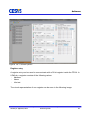
USBS6
USBS6 is a low-cost multilayer PCB with SPARTAN-6TM
FPGA and USB 2.0 Interface. 34 I/O balls of the FPGA are
available on standard 2.54mm headers, 81 I/O balls can be
reached through a industry standard VG 96-pin connector.
It offers multiple configuration options including USB and
onboard SPI-Flash and can also be used standalone
without the need of a USB interface.
UG107 (v1.1)April 07, 2014
www.cesys.com
1
Features
Features
USBS6 features
Form factor
120 x 100 mm
XILINX SPARTAN-6TM
XC6SLX16-2CSG324C
USB2.0 Controller
CYPRESSTM CY7C68013A
FPGA Configuration
Using USB2.0, JTAG or SPI-Flash
Memory
16Mb SPI-Flash Numonyx M25P16
128Mb Quad-SPI-Flash Macronix MX25L12845EMI-10G
1Gb low-power DDR SDRAM Micron
Technology MT46H64M16LFCK-5
Peripherals
USB to serial UART FTDI FT232R
HEX rotary DIP switch
3 status, 5 user LEDs
Expansion connectors
2 x 25-Pin standard RM2.54mm header
VG96-pin connector
Clock
Onboard 48 MHz clock signal
up to two optional onboard clocks
external clock sources possible
Included in delivery
The standard delivery includes:
•
One USBS6
•
One USB cable 1,5m
•
User's manual (English), drivers and source code of sample applications at our
download section at www.cesys.com.
All party are ROHS compliant.
UG107 (v1.1)April 07, 2014
www.cesys.com
2
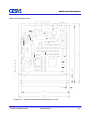
Hardware description
Hardware description
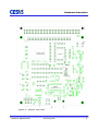
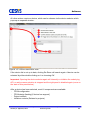
Block Diagram
Figure 1: USBS6 Block Diagram
Spartan-6TM FPGA
XC6SLX16-2CSG324C FPGA features
Logic cells
Configurable logic blocks (Slices/ Flip-Flops)
14,58
2,278/ 18,224
Max distributed RAM (kb)
136
DSP Slices
136
Block RAM Blocks (18kB/ Max(kb))
32/ 576
CMTs
UG107 (v1.1)April 07, 2014
2
www.cesys.com
3
Hardware description
For details of the SPARTAN-6TM FPGA device, please look at the data sheet at:
http://www.xilinx.com/support/documentation/data_sheets/ds160.pdf
UG107 (v1.1)April 07, 2014
www.cesys.com
4
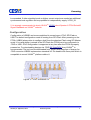
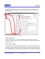
Hardware description
Figure 2: USBS6 Top View
UG107 (v1.1)April 07, 2014
www.cesys.com
5
Powering
Powering
USBS6 can be used bus-powered (see SW2 below) without the need of any external
power supply other than USB. In this mode VCCO_IO on J3 (A3, B3, C3) sourcing
capability is limited due to the fact, that USB power supply current is limited depending
on which system is used as host. In bus-powered mode, at first only FX2 is enabled.
After successful connection to the operating system the further power-on sequencing
behavior depends on UDK configuration. Until the release of UDK2.0 only the API could
enable power-on sequencing, therefore after plugging an USB cable it also was
necessary to start an application like cesys- Monitor before the FPGA and other devices
turned on. With v2.0 and upcoming releases of UDK framework the user can decide
which power-on behavior fits best. Power-on sequencing through API or as soon as
USB cable is plugged in. Default mode is API- controlled.
Mode of operation
SW2
Comment
VCCO_IO
Bus-powered
USB is used as power supply input.
3.3V @ 0,1A
Self-powered
Connect 5V power supply to VG-96pin
external expansion connector J3 PINS A1,
B1 und C1.
3.3V @ 2A**
Minimum required supply current: 400mA*
* The actually required supply current strongly depends on FGPA design and may exceed the
given minimum value.
** VCCO_IO current limit mainly depends on external power supply and may be less.
If USBS6 is used self-powered (see SW2 above), an external 5V power supply must be
connected to J3 (A1, B1, C1). In this mode all onboard voltages are enabled as soon as
an external power supply is applied. IO on J3 and J4 are powered through VCCO_IO on
BANK0 and BANK3. As default VCCO_IO is connected to VCCO/VCCAUX regulator to
enable 3.3V signaling levels on external expansion connectors J3 and J4. In selfpowered mode maximum current available for powering external hardware on J3 (A3,
B3, C3) mainly depends on the external power supply, but a maximum of 2A should not
UG107 (v1.1)April 07, 2014
www.cesys.com
6
Powering
be exceeded. If other signaling levels or higher current output are needed an additional
synchronous buck regulator can be populated to independently supply VCCO_IO.
! It is strongly recommended to check XILINXTM UG381 about Spartan-6 FPGA SelectIO
Signal Standards on XILINXTM website.
Configuration
Configuration of USBS6 can be accomplished in several ways: JTAG, SPI-Flash or
USB. The default configuration mode is booting from SPI-Flash. After powering on the
FPGA, USBS6 always tries to configure itself from the attached Flash using SPI Master
mode. If no valid design is stored in the SPI-Flash the FPGA has to be configured via
JTAG or USB. JTAG configuration is supported at any time after the FPGA is properly
powered on. For downloading designs via JTAG ISE WebPACK from XILINXTM is
recommended. The tool can be downloaded from XILINX web page free of charge. As
JTAG connector USBS6 implements a standard 2x7-Pin header with 2mm pitch which is
compatible to recent XILINXTM platform cables. #
Figure 3: JTAG connector J2
UG107 (v1.1)April 07, 2014
www.cesys.com
7
Powering
JTAG connector J2
PIN
Signal
Name
FPGA
IO
Comment
PIN
Signal
Name
FPGA
IO
Comment
1
GND
--
Ground signal
2
VCCAUX
--
3.3V auxiliary supply.
3
GND
--
Ground signal
4
TMS
B18
Test Mode Select.
5
GND
--
Ground signal
6
TCK
A17
Test Clock.
7
GND
--
Ground signal
8
TDO
D16
Test Data Out.
9
GND
--
Ground signal
10
TDI
D15
Test Data In.
11
GND
--
Ground signal
12
--
--
No connection.
13
GND
--
Ground signal
14
--
--
No connection.
For further information on the different configuration solutions for XILINXTM SPARTAN6TM FPGA the reader is encouraged to take a look at the user guide UG380 on
XILINXTM web page.
USB2.0 controller
CYPRESSTM FX2LPTM CY7C68013A is a highly integrated, low power USB2.0
microcontroller, that integrates USB2.0 transceiver, serial interface engine (SIE),
enhanced 8051 micro-controller and a programmable peripheral interface. More
information on usage of FX2LPTM in conjunction with Spartan-6 can be found in chapter
FPGA design.
Signal Name
FPGA
IO
Comment
FX2_IFCLK
V9
Clock input for both, FX2 and FPGA. 48MHz clock is provided by an
external oscillator.
FX2_SLWR
U8
FX2 input, FIFO write-strobe.
FX2_SLRD
T7
FX2 input, FIFO read-strobe.
FX2_SLOE
V11
FX2 input, output-enable, activates FX2 data bus.
FX2_PKTEND
V8
FX2 input, packet end control signal, causes FX2 to send data to host at
once, ignoring 512 byte alignment (so called “short packet”).
! Short packets sometimes lead to unpredictable behavior at host side,
wherefore short packets are not supported!
FX2_FIFOADR0
R10
FX2_FIFOADR1
U3
FX2 input, endpoint buffer addresses, only two endpoints are used:
EP2 (OUT, ADR[1:0] = b”00”) and EP6 (IN, ADR[1:0] = b”10”).
FX2_FLAGA
V16
FX2 output, EP2 “empty” flag.
FX2_FLAGB
U16
FX2 output, EP2 “almost empty” flag.
FX2_FLAGC
U11
FX2 output, EP6 “almost full” flag.
UG107 (v1.1)April 07, 2014
www.cesys.com
8
Powering
Signal Name
FPGA
IO
Comment
FX2_FD0
R11
16-Bit bidirectional FIFO data bus FD[0:15].
FX2_FD1
T14
FX2_FD2
V14
FX2_FD3
U5
FX2_FD4
V5
FX2_FD5
R3
FX2_FD6
T3
FX2_FD7
R5
FX2_FD8
N5
FX2_FD9
P6
FX2_FD10
P12
FX2_FD11
U13
FX2_FD12
V13
FX2_FD13
U10
FX2_FD14
R8
FX2_FD15
T8
External memory
USBS6 offers the opportunity to use various external memory architectures in one´s
FPGA design. With Micron Technology MT46H64M16LFCK-5 up to 1Gbit of high-speed
low-power DDR SDRAM is available. The integrated memory controller of Spartan-6TM
devices enables system designers to implement state-of-the-art memory interfaces
without the need to develop a whole memory controller Soft-IP all on their own. Some
examples on how to implement LPDDR with Spartan-6 are available in FPGA design.
Signal Name
FPGA IO
Comment
MCB1_A0
H15
MCB1_A1
H16
MCB1_A2
F18
MCB1_A3
J13
MCB1_A4
E18
Address inputs: Provide the row address for ACTIVE commands, and the
column address and auto precharge bit (A10) for READ or WRITE
commands, to select one location out of the memory array in the
respective bank. During a PRECHARGE command, A10 determines
whether the PRECHARGE applies to one bank (A10 LOW, bank selected by
BA0, BA1) or all banks (A10 HIGH). The address inputs also provide the
op-code during a LOAD MODE REGISTER command.
MCB1_A5
L12
MCB1_A6
L13
MCB1_A7
F17
UG107 (v1.1)April 07, 2014
www.cesys.com
9
Powering
Signal Name
FPGA IO
MCB1_A8
H12
MCB1_A9
G13
MCB1_A10
E16
MCB1_A11
G14
MCB1_A12
D18
MCB1_A13
C17
MCB1_BA0
H13
MCB1_BA1
H14
MCB1_RAS_n
K15
MCB1_CAS_n
K16
MCB1_WE_n
K12
MCB1_CS_n
--
MCB1_CKE_n
D17
Clock enable: CKE HIGH activates, and CKE LOW deactivates, the internal
clock signals, input buffers, and output drivers. Taking CKE LOW enables
PRECHARGE power-down and SELF REFRESH operations (all banks idle),
or ACTIVE power-down (row active in any bank). CKE is synchronous for
all functions except SELF REFRESH exit. All input buffers (except CKE) are
disabled during power-down and self refresh modes.
MCB1_RZQ
N14
Input termination calibration pin used with the soft calibration module.
External 100 Ohm resistor to GND.
MCB1_ZIO
Comment
Bank address inputs: BA0 and BA1 define to which bank an ACTIVE,
READ, WRITE, or PRECHARGE command is being applied. BA0 and BA1
also determine which mode register is loaded during a LOAD MODE
REGISTER command.
Command inputs: RAS#, CAS#, and WE# (along with CS#) define the
command being entered. *
No connect signal used with the soft calibration module to calibrate the
input termination value.
MCB1_CK
G16
MCB1_CK_n
G18
MCB1_DQ0
M16
MCB1_DQ1
M18
MCB1_DQ2
L17
MCB1_DQ3
L18
MCB1_DQ4
H17
MCB1_DQ5
H18
MCB1_DQ6
J16
MCB1_DQ7
J18
MCB1_LDQS
K17
UG107 (v1.1)April 07, 2014
Clock: CK is the system clock input. CK and CK# are differential clock
inputs. All address and control input signals are sampled on the crossing
of the positive edge of CK and the negative edge of CK#. Input and
output data is referenced to the crossing of CK and CK# (both directions
of the crossing).
Data input/output: Lower Byte Data bus.
Data strobe for Lower Byte Data bus: Output with read data, input with
write data. DQS is edge-aligned with read data, center-aligned in write
data. It is used to capture data.
www.cesys.com
10
Powering
Signal Name
FPGA IO
Comment
MCB1_LDM
L16
MCB1_UDM
L15
Input data mask: DM is an input mask signal for write data. Input data is
masked when DM is sampled HIGH along with that input data during a
WRITE access. DM is sampled on both edges of DQS.
MCB1_DQ8
N17
MCB1_DQ9
N18
MCB1_DQ10
P17
MCB1_DQ11
P18
MCB1_DQ12
T17
MCB1_DQ13
T18
MCB1_DQ14
U17
MCB1_DQ15
U18
MCB1_UDQS
N15
*
Data input/output: Upper Byte Data bus.
Data strobe for Upper Byte Data bus: Output with read data, input with
write data. DQS is edge-aligned with read data, center-aligned in write
data. It is used to capture data.
As the memory device interface of Spartan-6 supports only one device, CS# signal is not
supported by Spartan-6 MCB. CS# is pulled LOW via an external 0 Ohm resistor.
! It is strongly recommended to check XILINXTM user guide UG388 about Spartan-6TM
FPGA Memory Controller on XILINXTM website.
! It is strongly recommended to check XILINXTM user guide UG416 about Spartan-6TM
FPGA Memory Interface Solutions on XILINXTM website.
User specific data can be stored in up to 128Mb of non-volatile Flash-memory. The SPIcompliant interface guarantees ease of use and when speed matters
Macronix MX25L12845EMI-10G supports Q-SPI with data-rates up to 50 MByte/s in fast
read double transfer rate mode. Some examples on how to implement a SPI-compliant
interface with Spartan-6TM are available in chapter FPGA design.
Signal Name
FPGA IO
Comment
MX_CS_n
T6
Active- low Chip Select.
MX_SCLK
V4
Clock Input.
MX_SIO0
V6
Serial Data Input (SPI) / Serial Data IO (Dual- or Q- SPI).
MX_SIO1
T4
Serial Data Output (SPI) / Serial Data IO (Dual- or Q- SPI).
MX_SIO2
U7
Active- low Write Protect (SPI) / Serial Data IO (Dual- or Q-SPI).
MX_SIO3
V7
Not connect pin (SPI) / Serial Data IO (Dual- or Q-SPI).
UG107 (v1.1)April 07, 2014
www.cesys.com
11
Powering
Peripherals
USBS6 integrates several peripheral devices. Three system and five user- configurable
LEDs, one HEX rotary DIP switch and one USB to SERIAL UART are available. Power
supply status and FPGA configuration are observable through the system LEDs. The
user- configurable LEDs allow to make internal monitoring status signals visible by
driving the appropriate FPGA IO to a HIGH level.
Figure 4: USBS6 peripheral devices: System LEDs, User LEDs, USB-toSerial connector, HEX rotary DIP switch, USB2.0 connector
LEDs
Signal Name
FPGA IO
Comment
SYS_LED0
--
Internal 5V power supply.
SYS_LED1
--
Power OK- signal from onboard voltage regulator.
SYS_LED2
V17
Illuminates to indicate the status of the DONE pin if FPGA is successfully
configured.
USER_LED0
P7
User- configurable LED.
USER_LED1
N7
User- configurable LED.
USER_LED2
P8
User- configurable LED.
USER_LED3
N6
User- configurable LED.
USER_LED4
R7
User- configurable LED.
HEX rotary DIP switch
The HEX rotary DIP switch is of binary coded type. The four weighted terminals are
externally pulled HIGH with 4.7 kOhm resistors, the common terminals are connected to
GND. Therefore the four FPGA inputs behave like a complementary binary coded
hexadecimal switch.
UG107 (v1.1)April 07, 2014
www.cesys.com
12
Powering
DIAL
FPGA Pin N8
FPGA Pin M11
FPGA Pin M10
FPGA Pin N9
0
1
1
1
1
1
0
1
1
1
2
1
0
1
1
3
0
0
1
1
4
1
1
0
1
5
0
1
0
1
6
1
0
0
1
7
0
0
0
1
8
1
1
1
0
9
0
1
1
0
A
1
0
1
0
B
0
0
1
0
C
1
1
0
0
D
0
1
0
0
E
1
0
0
0
F
0
0
0
0
USB to serial UART interface
FT232R from FTDI is a USB to serial UART interface. A short example how to
implement a simple UART transceiver in FPGA designs can be found
hdl\usbs6\src\wb_sl_uart.vhd in UDKAPI2.0 installation folder.
Signal Name
FPGA
IO
Direction
Comment
FTDI_TXD
U15
FPGA IN
Transmit asynchronous data output for FT232R.
FTDI_RXD
V15
FPGA OUT
Receiving asynchronous data input for FT232R.
FTDI_RTS_n
N11
FPGA IN
Request to send control output for FT232R.
FTDI_CTS_n
M8
FPGA OUT
Clear to send control input for FT232R.
FTDI_RESET_n
T12
FPGA OUT
Active low reset pin for FT232R.
UG107 (v1.1)April 07, 2014
www.cesys.com
13
Powering
External expansion connectors
On connectors J3 and J4 up to 115 general purpose FPGA IO are accessible. Bank 0
and Bank 3 of the FPGA are configured for 3.3V signaling level per default. Differential
IO standards, as for example LVDS, are supported too. Detail information about IO
pairing is available in paragraph IO pairing and etch length report of chapter Additional
information.
! IO on connectors J3 and J4 are directly connected to FPGA IO and therefore are only
3.3 Volt tolerant. NEVER apply voltages outside the interval [-0.95V..4.1V] as this may
lead to severe damage of FPGA and attached components. For more information
regarding DC and switching characteristics of Spartan-6 FPGA please consult
documentation DS160 on XILINXTM website.
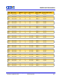
J3 VG96-pin external expansion connector
Figure 5: VG 96-pin external expansion connector J3
PIN
FPGA
IO
Comment
PIN
FPGA
IO
Comment
PIN
FPGA
IO
Comment
A32
--
GND
B32
--
GND
C32
--
GND
A31
F13
VG96_IO78
B31
E13
VG96_IO79
C31
C4
VG96_IO80
A30
F12
VG96_IO75
B30
E12
VG96_IO76
C30
F11
VG96_IO77
A29
D11
VG96_IO72*
B29
C11
VG96_IO73*
C29
E11
VG96_IO74
A28
G11
VG96_IO69
B28
F10
VG96_IO70
C28
G8
VG96_IO71
A27
G9
VG96_IO66
B27
F9
VG96_IO67
C27
F8
VG96_IO68
A26
D9
VG96_IO63*
B26
C9
VG96_IO64*
C26
D8
VG96_IO65
A25
E7
VG96_IO60
B25
E8
VG96_IO61
C25
C8
VG96_IO62
A24
D6
VG96_IO57
B24
C6
VG96_IO58
C24
F7
VG96_IO59
A23
F6
VG96_IO54
B23
F5
VG96_IO55
C23
E6
VG96_IO56
A22
--
GND
B22
--
GND
C22
--
GND
A21
E4
VG96_IO51
B21
D3
VG96_IO52
C21
F4
VG96_IO53
UG107 (v1.1)April 07, 2014
www.cesys.com
14
Powering
PIN
FPGA
IO
Comment
PIN
FPGA
IO
Comment
PIN
FPGA
IO
Comment
A20
H7
VG96_IO48
B20
G6
VG96_IO49
C20
F3
VG96_IO50
A19
H4
VG96_IO45*
B19
H3
VG96_IO46*
C19
J7
VG96_IO47
A18
H6
VG96_IO42
B18
H5
VG96_IO43
C18
J6
VG96_IO44
A17
K4
VG96_IO39*
B17
K3
VG96_IO40*
C17
L6
VG96_IO41
A16
L7
VG96_IO36
B16
K6
VG96_IO37
C16
M5
VG96_IO38
A15
L5
VG96_IO33*
B15
K5
VG96_IO34*
C15
E3
VG96_IO35
A14
L4
VG96_IO30
B14
L3
VG96_IO31
C14
E1
VG96_IO32
A13
C2
VG96_IO27
B13
C1
VG96_IO28
C13
G3
VG96_IO29
A12
D2
VG96_IO24
B12
D1
VG96_IO25
C12
G1
VG96_IO26
A11
F2
VG96_IO21
B11
F1
VG96_IO22
C11
J3
VG96_IO23
A10
H2
VG96_IO18*
B10
H1
VG96_IO19*
C10
J1
VG96_IO20
A9
K2
VG96_IO15
B9
K1
VG96_IO16
C9
M3
VG96_IO17
A8
L2
VG96_IO12
B8
L1
VG96_IO13
C8
M1
VG96_IO14
A7
N2
VG96_IO9
B7
N1
VG96_IO10
C7
N4
VG96_IO11
A6
P2
VG96_IO6
B6
P1
VG96_IO7
C6
N3
VG96_IO8
A5
T2
VG96_IO3
B5
T1
VG96_IO4
C5
P4
VG96_IO5
A4
U2
VG96_IO0
B4
U1
VG96_IO1
C4
P3
VG96_IO2
A3
--
VCCO_IO
B3
--
VCCO_IO
C3
--
VCCO_IO
A2
--
GND
B2
--
GND
C2
--
GND
A1
--
5.0V_EXT
B1
--
5.0V_EXT
C1
--
5.0V_EXT
* GCLK
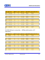
J4 IDC 2x25-Pin external expansion connector
Figure 6: IDC 2x25-Pin external expansion connector J4
UG107 (v1.1)April 07, 2014
www.cesys.com
15
Powering
PIN
FPGA IO
Comment
PIN
FPGA IO
Comment
1
--
VCCO_IO
2
--
GND
3
C5
ADD_IO0
4
A5
ADD_IO1
5
C7
ADD_IO2
6
A7
ADD_IO3
7
--
GND
8
--
GND
9
B2
ADD_IO4
10
A2
ADD_IO5
11
B3
ADD_IO6
12
A3
ADD_IO7
13
B4
ADD_IO8
14
A4
ADD_IO9
15
B6
ADD_IO10
16
A6
ADD_IO11
17
--
GND
18
--
GND
19
B8
ADD_IO12
20
A8
ADD_IO13
21
B9
ADD_IO14*
22
A9
ADD_IO15*
23
--
GND
24
--
GND
25
B11
ADD_IO16
26
A11
ADD_IO17
27
B12
ADD_IO18
28
A12
ADD_IO19
29
B14
ADD_IO20
30
A14
ADD_IO21
31
B16
ADD_IO22
32
A16
ADD_IO23
33
--
GND
34
--
GND
35
C10
ADD_IO24*
36
A10
ADD_IO25*
37
D12
ADD_IO26
38
C12
ADD_IO27
39
--
GND
40
--
GND
41
C13
ADD_IO28
42
A13
ADD_IO29
43
D14
ADD_IO30
44
C14
ADD_IO31
45
C15
ADD_IO32
46
A15
ADD_IO33
47
D4
HSWAPEN**
48
--
GND
49
--
VCCO_IO
50
--
GND
* GCLK
** Enable / Disable optional pull-up resistors during configuration. Pulled HIGH via external
4.7 kOhm resistor. Leave unconnected.
! It is strongly recommended to check the appropriate data sheets of SPARTAN-6
TM
devices about special functionality IO like GCLK, HSWAPEN, …
UG107 (v1.1)April 07, 2014
www.cesys.com
16
Powering
Suspend and Awake
SPARTAN-6TM FPGA devices support an advanced static power-management feature,
which reduces power consumption while retaining the FPGA's configuration data and
maintaining the design.
Figure 7: Awake LED and Suspend
Connector J1
J1 FPGA Suspend connector
PIN
FPGA IO
Signal Name
Comment
1
R16
SUSPEND
Active-High control input pin for the power-saving Suspend
mode. Must be enabled by configuration option. Pulled LOW via
external 4.7 kOhm resistor.
2
--
VCCAUX
3.3V auxiliary supply
3
--
VCCAUX
3.3V auxiliary supply
Awake LED
Signal Name
FPGA IO
Comment
AWAKE
P15
Indicates the present suspend mode status using the AWAKE pin.
Bitstream option needs to be set to drive_awake:yes.
If Suspend mode is disabled in user application, AWAKE is available as
user I/O. Drive High to light onboard AWK-LED.
For details of the Suspend feature of SPARTAN-6 TM devices, please visit XILINXTM
homepage and check User Guide Spartan-6 FPGA Power Management.
UG107 (v1.1)April 07, 2014
www.cesys.com
17
FPGA design
FPGA design
Cypress FX-2 LP and USB basics
Several data transfer types are defined in USB 2.0 specification. High-speed bulk
transfer is the one and only mode of interest to end users. USB transfers are packet
oriented and have a time framing scheme. USB packets consist of USB protocol and
user payload data. Payload could have a variable length of up to 512 bytes per packet.
Packet size is fixed to the maximum value of 512 bytes for data communication with
CESYS USB cards to achieve highest possible data throughput. USB peripherals could
have several logical channels to the host. The data source/sink for each channel inside
the USB peripheral is called the USB endpoint. Each endpoint can be configured as
“IN”- (channel direction: peripheral => host) or “OUT”-endpoint (channel direction: host
=> peripheral) from host side perspective. CESYS USB cards support two endpoints,
one for each direction. FX-2 has an integrated USB SIE (Serial Interface Engine)
handling USB protocol and transferring user payload data to the appropriate endpoint.
So end users do not have to care about USB protocol in their own applications. FX-2
endpoints are realized as 2 kB buffers. These buffers can be accessed over a FIFO-like
interface with a 16 bit tristate data bus by external hardware. External hardware acts as
a master, polling FIFO flags, applying read- and write-strobes and transferring data.
Therefore this FX-2 data transfer mechanism is called “slave FIFO mode”. As already
mentioned, all data is transferred in multiples of 512 bytes. External hardware has to
ensure, that the data written to IN-endpoint is aligned to this value, so that data will be
transmitted from endpoint buffer to host. The 512 byte alignment normally causes no
restrictions in data streaming applications with endless data transfers. Maybe it is
necessary to fill up endpoint buffer with dummy data, if some kind of host timeout
condition has to be met. Another FX-2 data transfer mechanism is called “GPIF
(General Programmable InterFace) mode”. The GPIF engine inside the FX-2 acts as a
master to endpoint buffers, transferring data and presenting configurable handshake
waveforms to external hardware. CESYS USB card supports “slave FIFO mode” for
data communication only. “GPIF mode” is exclusively used for downloading
configuration bitstreams to FPGA.
UG107 (v1.1)April 07, 2014
www.cesys.com
18
FPGA design
Clocking FPGA designs
The 48 MHz SYSCLK oscillator is an onboard clock source for the FPGA. It is used as
interface clock (IFCLK) between FX-2 slave FIFO bus and FPGA I/Os. So this clock
source must be used for data transfers to and from FPGA over USB! Appropriate timing
constraints can be found in “*.ucf”-files of design examples included in delivery.
It is strictly recommended to use a single clock domain whenever possible. Using a fully
synchronous system architecture often results in smaller, less complex and more
performant FPGA designs (compare XilinxTM white paper WP331 “Timing
Closure/Coding Guidelines”).
In FPGA designs with multiple clock domains asynchronous FIFOs have to be used for
transferring data from one clock domain to the other and comprehensive control signals
have to be resynchronized.
Other clock sources can be added internally by using Spartan-6TM onchip digital clock
managers (DCMs) or PLLs or externally by connecting clock sources to other FPGA
global clock inputs. A wide range of clock frequencies can be synthesized with DCMs
and PLLs. For further details on DCMs/PLLs please see “Spartan-6TM FPGA Clocking
Resources User Guide UG382”.
FX-2/FPGA slave FIFO connection
Only the logical behavior of slave FIFO interface is discussed here. For information
about the timing behavior like setup- and hold-times please see FX-2 datasheet.
All flags and control signals are active low (postfix “#”). The whole interface is
synchronous to IFCLK. The asynchronous FIFO transfer mode is not supported.
Flags & control
signals
Comment
SLWR#
FX-2 input, FIFO write-strobe
SLRD#
FX-2 input, FIFO read-strobe
SLOE#
FX-2 input, output-enable, activates FX-2 data bus drivers
PKTEND#
FX-2 input, packet end control signal, causes FX-2 to send data to host at once,
ignoring 512 byte alignment (so called “short packet”)
Short packets sometimes lead to unpredictable behavior at host side. So CESYS USB cards do not
support short packets! This signal has to be statically set to HIGH! Dummy data should be added
instead of creating short packets. There is normally no lack of performance by doing this, because
transmission of USB packets is bound to a time framing scheme, regardless of amount of payload
UG107 (v1.1)April 07, 2014
www.cesys.com
19
FPGA design
Flags & control
signals
Comment
data.
FIFOADR[1:0]
FX-2 input, endpoint buffer addresses, CESYS USB cards use only two endpoints
EP2 (OUT, ADR[1:0] = b”00”) and EP6 (IN, ADR[1:0] = b”10”)
Switching FIFOADR[1] is enough to select data direction. FIFOADR[0] has to be statically set to LOW!
FLAG#-A/-B/-C
FX-2 outputs, A => EP2 “empty” flag, B => EP2 “almost empty” flag, meaning
one 16 bit data word is available, C => EP6 “almost full” flag, meaning one 16 bit
data word can still be transmitted to EP6, there is no real “full” flag for EP6,
“almost full” could be used instead
FD[15:0]
bidirectional tristate data bus
Introduction to example FPGA designs
The CESYS USBS6 Card is shipped with some demonstration FPGA designs to give
you an easy starting point for own development projects. The whole source code is
written in VHDL. Verilog and schematic entry design flows are not supported.
•
The design “usbs6_soc” demonstrates the implementation of a system-on-chip
(SoC) with host software access to the peripherals like GPIOs, external Flash
Memory, LPDDR Memory and internal BlockRAM over USB. This design requires a
protocol layer over the simple USB bulk transfer (see CESYS application note
“Transfer Protocol for CESYS USB products” for details), which is already provided
by CESYS software API.
•
The design “usbs6_bram” is a minimal example for data transfers from and to the
FPGA over USB and can be used to get for familiar with UDK hardware/software
interface.
The Spartan-6 XC6SLX16 Device is supported by the free XilinxTM ISE Webpack
development software. You will have to change some options of the project properties
for own applications.
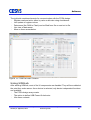
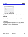
A bitstream in the “*.bin”-format is needed, if you want to download your FPGA design
with the CESYS software API-functions LoadBIN() and ProgramFPGA(). The
generation of this file is disabled by default in the XilinxTM ISE development
environment. Check “create binary configuration file” at right click “generate
programming file”=>properties=>general options:
UG107 (v1.1)April 07, 2014
www.cesys.com
20
FPGA design
After ProgramFPGA() is called and the FPGA design is completely downloaded, the
pin #RESET (note: the prefix # means, that the signal is active low) is automatically
pulsed (HIGH/LOW/HIGH). This signal can be used for resetting the FPGA design. The
API-function ResetFPGA() can be called to initiate a pulse on #RESET at a user given
time.
The following sections will give you a brief introduction about the data transfer from and
to the FPGA over the Cypress FX-2 USB peripheral controller's slave FIFO interface,
the WISHBONE interconnection architecture and the provided peripheral controllers.
CESYS USB cards use only slave FIFO mode for transferring data. For further
information about the FX-2 slave FIFO mode see Cypress FX-2 user manual and
datasheet and about the WISHBONE architecture see specification B.3
(wbspec_b3.pdf).
UG107 (v1.1)April 07, 2014
www.cesys.com
21
FPGA design
FPGA source code copyright information
This source code is copyrighted by CESYS GmbH / GERMANY, unless otherwise
noted.
FPGA source code license
THIS SOURCECODE IS NOT FREE! IT IS FOR USE TOGETHER WITH THE CESYS
PRODUCTS ONLY!
YOU ARE NOT ALLOWED TO MODIFY AND DISTRIBUTE OR USE IT WITH ANY
OTHER HARDWARE, SOFTWARE OR ANY OTHER KIND OF ASIC OR
PROGRAMMABLE LOGIC DESIGN WITHOUT THE EXPLICIT PERMISSION OF THE
COPYRIGHT HOLDER!
Disclaimer of warranty
THIS SOURCECODE IS DISTRIBUTED IN THE HOPE THAT IT WILL BE USEFUL,
BUT THERE IS NO WARRANTY OR SUPPORT FOR THIS SOURCECODE. THE
COPYRIGHT HOLDER PROVIDES THIS SOURCECODE “AS IS” WITHOUT
WARRANTY OF ANY KIND, EITHER EXPRESSED OR IMPLIED, INCLUDING, BUT
NOT LIMITED TO, THE IMPLIED WARRANTIES OF MERCHANTABILITY AND
FITNESS FOR A PARTICULAR PURPOSE. THE ENTIRE RISK AS TO THE QUALITY
AND PERFORMANCE OF THIS SOURCECODE IS WITH YOU. SHOULD THIS
SOURCECODE PROVE DEFECTIVE, YOU ASSUME THE COST OF ALL
NECESSARY SERVICING, REPAIR OR CORRECTION. IN NO EVENT WILL THE
COPYRIGHT HOLDER BE LIABLE TO YOU FOR DAMAGES, INCLUDING ANY
GENERAL, SPECIAL, INCIDENTAL OR CONSEQUENTIAL DAMAGES ARISING OUT
OF THE USE OR INABILITY TO USE THIS SOURCECODE (INCLUDING BUT NOT
LIMITED TO LOSS OF DATA OR DATA BEING RENDERED INACCURATE OR
LOSSES SUSTAINED BY YOU OR THIRD PARTIES OR A FAILURE OF THIS
SOURCECODE TO OPERATE WITH ANY OTHER SOFTWARE-PROGRAMS,
HARDWARE-CIRCUITS OR ANY OTHER KIND OF ASIC OR PROGRAMMABLE
LOGIC DESIGN), EVEN IF THE COPYRIGHT HOLDER HAS BEEN ADVISED OF THE
POSSIBILITY OF SUCH DAMAGES.
UG107 (v1.1)April 07, 2014
www.cesys.com
22
FPGA design
Design “usbs6_soc”
An on-chip-bus system is implemented in this design. The VHDL source code shows
you, how to build a 32 Bit WISHBONE based shared bus architecture. All devices of the
WISHBONE system support only SINGLE READ / WRITE Cycles. Files and modules
having something to do with the WISHBONE system are labeled with the prefix “wb_”.
The WISHBONE master is labeled with the additional prefix “ma_” and the slaves are
labeled with “sl_”. There is a package for each module with the additional postfix “_pkg”.
It contains the appropriate VHDL component declaration / interface description as well
as public constants like register address offsets.
UG107 (v1.1)April 07, 2014
www.cesys.com
23
FPGA design
Files and modules
Comment
src/wishbone_pkg.vhd
A package containing datatypes, constants, and components needed for the
WISHBONE system. There are VHDL subroutines for a WISHBONE master bus
functional model (BFM), too. These can be used for behavioral simulation
purposes.
src/usbs6_soc_top.vhd
This is the top level entity of the design. The WISHBONE components are
instantiated here.
src/wb_intercon.vhd
All WISHBONE devices are connected to this shared bus interconnection logic.
Some MSBs of the address are used to select the appropriate slave.
src/wb_ma_fx2.vhd
This is the entity of the WISHBONE master, which converts the CESYS USB
protocol into one or more 32 Bit single read/write WISHBONE cycles. The low
level FX-2 slave FIFO controller (fx2_slfifo_ctrl.vhd) is used and 16/32 bit data
width conversion is done by using special FIFOs
(sfifo_hd_a1Kx18b0K5x36.vhd).
src/wb_sl_bram.vhd
A internal BlockRAM is instantiated here and simply connected to the
WISHBONE architecture. It can be used for testing address oriented data
transactions over USB.
src/wb_sl_gpio.vhd
This entity provides up to 256 general purpose I/Os to set and monitor nontiming-critical internal and external FPGA signals. The I/Os can be accessed as
eight ports with 32 bits each. Every single I/O can be configured as an in- or
output.
I/O signals of VG96 connector VG96_IO[80:0] are at port0 – port2, bits[80:0],
I/O signals of add-on connector ADD_IO[33:0] are at port3 – port4,
bits[129:96], user LEDs are at port5, bits[163:160] and hex encoder is at
port6, bits[195:192].
Port7 is used for monitoring MCB status signals bit[224] => READ ERROR,
bit[225] => READ OVERFLOW, bit[226] => WRITE ERROR, bit[227] => WRITE
UNDERRUN and bit[228] => CALIBRATION DONE.
src/wb_sl_flash.vhd
The module encapsulates the low level FLASH controller flash_ctrl.vhd. The
integrated command register supports the BULK ERASE command, which
erases the whole memory by programming all bits to '1'. In write cycles the bit
values can only be changed from '1' to '0'. That means, that it is not allowed to
have a write access to the same address twice without erasing the whole flash
before. The read access is as simple as reading from any other WISHBONE
device. Please see the SPI-FLASH data sheet for details on programming and
erasing. There are two instances of this module. One is used for programming
FPGA configuration bitstream to SPI-FLASH and the other accesses QUAD-SPIFLASH for storing nonvolatile application data.
src/wb_sl_mcb.vhd
WISHBONE adapter for one port of Spartan-6TM build in multiport memory
controller block (MCB).
UG107 (v1.1)April 07, 2014
www.cesys.com
24
FPGA design
Files and modules
Comment
src/wb_sl_uart.vhd
This entity is a simple UART transceiver with 16 byte buffer for each direction
TM
connected to USB2UART interface. Xilinx
UART transceiver macros are used
as physical layer. Baudrate is adjustable up to 230400 (default: 9600) by
writing appropriate timer prescaling values to the status and configuration
register. This register contains buffer level flags FULL and HALFFULL for each
direction, too. Data format is fixed at 8-N-1. Reading from UART pipe is always
non-blocking. A data present flag provided along with received bytes indicates,
if current RX value is valid. Writing to UART pipe is blocking, if TX buffer gets
full. So that loss of transmitted data can easily be avoided.
src/xil_uart_macro/
TM
This directory contains VHDL source code files of Xilinx
UART transceiver
TM
macros. Note that these source code files are copyrighted by Xilinx
and are
absolutely not supported by CESYS! For details on these macros see the
application note “XAPP223 - 200 MHz UART with Internal 16-Byte Buffer”
TM
provided by Xilinx
.
TM
src/xil_mcb_mig/
This directory contains VHDL source code files generated by Xilinx
memory
interface generator tool to build the frontend for MCB. File
memc1_infrastructure.vhd has been modified to fit example design
requirements.
src/fx2_slfifo_ctrl.vhd
This controller handles 512 byte aligned raw USB bulk transfers without CESYS
USB transfer protocol. It checks FX-2 FIFO flags and copies data from FX-2
endpoints to internal FPGA buffers (sync_fifo.vhd) and vice versa. So the USB
data link looks like any other FPGA FIFO buffer to user logic. Ports of
fx2_slfifo_ctrl connected to FX-2 are labeled with prefix fx2_ and ports
connected to user logic are labeled with prefix app_. Sometimes the
abbreviations _h2p_ (host to peripheral) and _p2h_ (peripheral to host) are
used in signal names to indicate data flow direction.
The upper waveform demonstrates the behavior of app_fifo_wr_full_o and
UG107 (v1.1)April 07, 2014
www.cesys.com
25
FPGA design
app_fifo_wr_count_o when there is no transaction on the slave FIFO controller side
of the FIFO. During simultaneous FIFO-read- and FIFO-write-transactions, the signals
do not change. The signal app_fifo_wr_full_o will be cleared and
app_fifo_wr_count_o will decrease, if there are read-transactions at the slave FIFO
controller side, but no write-transactions at the application side.
The lower waveform demonstrates the behavior of app_fifo_rd_empty_o and
app_fifo_rd_count_o when there is no transaction at the slave FIFO controller side
of the FIFO. During simultaneous FIFO-read- and FIFO-write-transactions, the signals
do not change. The signal app_fifo_rd_empty_o will be cleared and
app_fifo_rd_count_o will increase, if there are write-transactions on the slave FIFO
controller side, but no read-transactions at the application side. Please note the one
clock-cycle delay between app_fifo_rd_i and app_fifo_rd_data_o!
The signals app_usb_h2p_pktcount_o[7:0] and
app_usb_p2h_pktcount_o[7:0] (not shown in figure 9) are useful to fit the 512
byte USB bulk packet alignment. They are automatically incremented, if the
appropriate read- (app_fifo_rd_i) or write-strobe (app_fifo_wr_i) is asserted.
These signals count 16 bit data words, not data bytes! 512 byte alignment is turned into
a 256 16 bit word alignment at this interface.
Please note, that using raw USB bulk transfers and slave FIFO transactions directly is
not recommended! It is just for background information. Use protocol based
WISHBONE interface instead!
Files and modules
Comment
src/sync_fifo.vhd
This entity is a general purpose synchronous FIFO buffer. It is build
of FPGA distributed RAM.
src/sfifo_hd_a1Kx18b0K5x36.vhd
This entity is a general purpose synchronous FIFO buffer with
mismatched port widths. It is build of a FPGA BlockRAM.
src/flash_ctrl.vhd
The low level FLASH controller for SPI FLASH memory. It supports
reading and writing of four bytes of data at one time as well as
erasing the whole memory.
usbs6_soc.xise
Project file for Xilinx
usbs6_soc.ucf
User constraint file with timing and pinout constraints
usbs6_soc_fpga_consts.h
C header file extracted from VHDL packages. It contains address,
flag, bitfield and value definitions for FPGA design access integration
into host software application.
UG107 (v1.1)April 07, 2014
TM
ISE
www.cesys.com
26
FPGA design
Software Pseudo-Code Example
#include “usbs6_soc_fpga_consts.h”
/* address of UART status and configuration register */
uint32_t uiRegAddr = UART_BASEADR + UART_STACFG_OFFSET;
/* read-modify-write register value for 9600 baud */
uint32_t uiRegVal = ReadRegister(uiRegAddr) & (~UART_STACFG_BDR_FIELD);
uiRegVal |=
UART_STACFG_BDR_FIELD &
(UART_STACFG_BDR_VAL_9600<<UART_STACFG_BDR_FIELD_POS);
/* setting UART baud rate */
WriteRegister(uiRegAddr, uiRegVal);
WISHBONE transactions
The software API-functions ReadRegister(), WriteRegister() lead to one and
ReadBlock(), WriteBlock() to several consecutive WISHBONE single cycles.
Bursting is not allowed in the WISHBONE demo application. The address can be
incremented automatically in block transfers. You can find details on enabling/disabling
the burst mode and address auto-increment mode in the CESYS application note
“Transfer Protocol for CESYS USB products” and software API documentation.
CESYS USB transfer protocol is converted into one or more WISHBONE data
transaction cycles. So the FX-2 becomes a master device in the internal WISHBONE
architecture. Input signals for the WISHBONE master are labeled with the postfix “_I”,
output signals with “_O”.
WISHBONE signals driven by the master:
STB_O: strobe, qualifier for the other output signals of the master, indicates valid data and control
signals
WE_O: write enable, indicates, if a write or read cycle is in progress
ADR_O[31:2]: 32-Bit address bus, the software uses BYTE addressing, but all internal WISHBONE
accesses are DWORD (32-Bit) aligned. So address LSBs [1:0] are discarded.
DAT_O[31:0]: 32-Bit data out bus for data transportation from master to slaves
UG107 (v1.1)April 07, 2014
www.cesys.com
27
FPGA design
WISHBONE signals driven by slaves:
DAT_I[31:0]: 32-Bit data in bus for data transportation from slaves to master
ACK_I: handshake signal, slave devices indicate a successful data transfer for writing and valid data on
bus for reading by asserting this signal, slaves can insert wait states by delaying this signal, it is possible
to assert ACK_I in first clock cycle of STB_O assertion using a combinatorial handshake to transfer data
in one clock cycle (recommendation: registered feedback handshake should be used in applications,
where maximum data throughput is not needed, because timing specs are easier to meet)
UG107 (v1.1)April 07, 2014
www.cesys.com
28
FPGA design
Figure 11: WISHBONE transactions with WriteRegister()
WriteBlock() ReadRegister() ReadBlock()
The WISHBONE signals in these illustrations and explanations are shown as simple bit
types or bit vector types, but in the VHDL code these signals could be encapsulated in
extended data types like arrays or records.
UG107 (v1.1)April 07, 2014
www.cesys.com
29
FPGA design
Example:
...
port map
(
...
ACK_I => intercon.masters.slave(2).ack,
...
Port ACK_I is connected to signal ack of element 2 of array slave, of record masters, of
record intercon.
Design “usbs6_bram”
This design is intended to demonstrate behavior of UDK software API resulting in
WISHBONE cycles. It is a reduced version of “usbs6_soc” example implementing a
single BlockRAM slave.
Files and modules
Comment
src/wishbone_pkg.vhd
See chapter “Design usbs6_soc”
src/usbs6_bram_top.vhd
This is the top level module. It instantiates FX-2 module as a
WISHBONE master device (wb_ma_fx2.vhd) and a BlockRAM as a
WISHBONE slave device (wb_sl_bram.vhd).
src/wb_ma_fx2.vhd
See chapter “Design usbs6_soc”
src/wb_sl_bram.vhd
See chapter “Design usbs6_soc”
src/sim_tb/wb_sl_bram_tb.vhd
Example of a VHDL simulation testbench demonstrating BFM
techniques for accessing BlockRAM as a WISHBONE slave device
(wb_sl_bram.vhd).
src/fx2_slfifo_ctrl.vhd
See chapter “Design usbs6_soc”
src/sync_fifo.vhd:
See chapter “Design usbs6_soc”
usbs6_bram.xise:
Project file for XilinxTM ISE.
usbs6_bram.ucf:
User constraint file with timing and pinout constraints.
wb_sl_bram_tb.do:
ModelSim command macro file for BFM BlockRAM testbench
(wb_sl_bram_tb.vhd).
wb_sl_bram_tb.cmd:
Win32 batch file automatically starting ModelSim with example
testbench and appropriate simulation script (wb_sl_bram_tb.do).
Just doubleclick for running the demo!
UG107 (v1.1)April 07, 2014
www.cesys.com
30
Software
Software
The UDK (Unified Development Kit) is used to allow developers to communicate with
Cesys's USB and PCI(e) devices. Older releases were just a release of USB and PCI
drivers plus API combined with some shared code components. The latest UDK
combines all components into one single C++ project and offers interfaces to C++, C
and for .NET (Windows only). The API has functions to mask-able enumeration, unique
device identification (runtime), FPGA programming and 32bit bus based data
communication. PCI devices have additional support for interrupts.
Changes to previous versions
Beginning with release 2.0, the UDK API is a truly combined interface to Cesys's USB
and PCI devices. The class interface from the former USBUni and PCIBase API's was
saved at a large extend, so porting applications from previous UDK releases can be
done without much work.
Here are some notes about additional changes:
•
Complete rewrite
•
Build system cleanup, all UDK parts (except .NET) are now part of one large project
•
64 bit operating system support
•
UDK tools combined into one application (UDKLab)
•
Updated to latest PLX SDK (6.31)
•
Identical C, C++ and .NET API interface (.NET ⇒ Windows only)
•
Different versions of components collapsed to one UDK version
•
Windows only:
◦
Microsoft Windows Vista / Seven(7) support (PCI drivers are not released for
Seven at the moment)
◦
Driver installation / update is done by an installer now
◦
Switched to Microsoft's generic USB driver (WinUSB)
◦
Support moved to Visual Studio 2005, 2008 and 2010(experimental), older
Visual Studio versions are not supported anymore
•
Linux only:
◦
Revisited USB driver, tested on latest Ubuntu distributions (32/64)
◦
Simpler USB driver installation
UG107 (v1.1)April 07, 2014
www.cesys.com
31
Software
Windows
Requirements
To use the UDK in own projects, the following is required:
•
Installed drivers
•
Microsoft Visual Studio 2005 or 2008; 2010 is experimental
•
CMake 2.6 or higher ⇒ http://www.cmake.org
•
wxWidgets 2.8.10 or higher (must be build separately) ⇒ http://www.wxwidgets.org
[optionally, only if UDKLab should be build]
Driver installation
The driver installation is part of the UDK installation but can run standalone on final
customer machines without the need to install the UDK itself. During installation, a
choice of drivers to install can be made, so it is not necessary to install i.e. PCI drivers
on machines that should run USB devices only or vice versa. If USB drivers get installed
on a machine that has a pre-2.0 UDK driver installation, we prefer the option for USB
driver cleanup offered by the installer, this cleanly removes all dependencies of the old
driver installation.
Note: There are separate installers for 32 and 64 bit systems.
Important: At least one device should be present when installing the drivers !
Build UDK
Prerequisites
The most components of the UDK are part of one large CMake project. There are some
options that need to be fixed in msvc.cmake inside the UDK installation root:
•
•
•
BUILD_UI_TOOLS If 0, UDKLab will not be part of the subsequent build procedure,
if 1 it will. This requires an installation of an already built wxWidgets.
WX_WIDGETS_BASE_PATH Path to wxWidgets build root, only needed if
BUILD_UI_TOOLS is not 0.
USE_STATIC_RTL If 0, all projects are build against the dynamic runtime libraries.
This requires the installation of the appropriate Visual Studio redistributable pack on
every machine the UDK is used on. Using a static build does not create such
dependencies, but will conflict with the standard wxWidgets build configuration.
UG107 (v1.1)April 07, 2014
www.cesys.com
32
Software
Solution creation and build
The preferred way is to open a command prompt inside the installation root of the UDK,
lets assume to use c:\\udkapi.
c:
cd \udkapi
CMake allows the build directory separated to the source directory, so it's a good idea to
do it inside an empty sub-directory:
mkdir build
cd build
The following code requires an installation of CMake and at least one supported Visual
Studio version. If CMake isn't included into the PATH environment variable, the path
must be specified as well:
cmake ..
This searches the preferred Visual Studio installation and creates projects for it. Visual
Studio Express users may need to use the command prompt offered by their
installation. If multiple Visual Studio versions are installed, CMake's command
parameter '-G' can be used to specify a special one, see CMake's documentation in this
case. This process creates the solution files inside c:\\udkapi\\build. All subsequent
tasks can be done in Visual Studio (with the created solution), another invocation of
CMake isn't necessary under normal circumstances.
Important: The UDK C++ API must be build with the same toolchain and build flags like
the application that uses it. Otherwise unwanted side effects in exception handling will
occur ! (See example in Add project to UDK build).
Info: It is easy to create different builds with different Visual Studio versions by creating
different build directories and invoke CMake with different '-G' options inside them:
c:
cd \udkapi
mkdir build2005
cd build2005
UG107 (v1.1)April 07, 2014
www.cesys.com
33
Software
cmake -G"Visual Studio 8 2005" ..
cd ..
mkdir build2008
cd build2008
cmake -G"Visual Studio 9 2008" ..
Linux
There are too many distributions and releases to offer a unique way to the UDK
installation. We've chosen to work with the most recent Ubuntu release, 9.10 at the
moment. All commands are tested on an up to date installation and may need some
tweaking on other systems / versions.
Requirements
•
•
•
•
GNU C++ compiler toolchain
zlib development libraries
CMake 2.6 or higher ⇒ http://www.cmake.org
wxWidgets 2.8.10 or higher ⇒ http://www.wxwidgets.org [optionally, only if UDKLab
should be build]
sudo apt-get install build-essential cmake zlib1g-dev libwxbase2.8-dev
libwxgtk2.8-dev
The Linux UDK comes as gzip'ed tar archive, as the Windows installer won't usually
work. The best way is to extract it to the home directory:
tar xzvf UDKAPI-x.x.tgz ~/
This creates a directory /home/[user]/udkapi[version] which is subsequently called
udkroot. The following examples assume an installation root in ~/udkapi2.0.
Important: Commands sometimes contain a ` symbol, have attention to use the right
one, refer to command substitution if not familiar with.
Driver installation
The driver installation on Linux systems is a bit more complicated than on Windows
systems. The drivers must be build against the installed kernel version. Updating the
kernel requires a rebuild.
UG107 (v1.1)April 07, 2014
www.cesys.com
34
Software
USB
As the USB driver is written by Cesys, the installation procedure is designed to be as
simple and automated as possible. The sources and support files reside in directory
<udkroot>/drivers/linux/usb. Just go there and invoke make.
cd ~/udkapi2.0/drivers/linux/usb
make
If all external dependencies are met, the build procedure should finish without errors.
Newer kernel releases may change things which prevent success, but it is out of the
scope of our possibilities to be always up-to-date with latest kernels. To install the driver,
the following command has to be done:
sudo make install
This will do the following things:
•
Install the kernel module inside the module library path, update module
dependencies
•
Install a new udev rule to give device nodes the correct access rights (0666)
(/etc/udev/rules.d/99-ceusbuni.rules)
•
Install module configuration file (/etc/dev/modprobe.d/ceusbuni.conf)
•
Start module
If things work as intended, there must be an entry /proc/ceusbuni after this procedure.
The following code will completely revert the above installation (called in same
directory):
sudo make remove
The configuration file, /etc/modprobe.d/ceusbuni.conf, offers two simple options (Read
the comments in the file):
•
Enable kernel module debugging
•
Choose between firmware which automatically powers board peripherals or not
Changing these options require a module reload to take affect.
PCI
The PCI drivers are not created or maintained by Cesys, they are offered by the
manufacturer of the PCI bridges that were used on Cesys PCI(e) boards. So problems
UG107 (v1.1)April 07, 2014
www.cesys.com
35
Software
regarding them can't be handled or supported by us.
Important: If building PlxSdk components generate the following error / warning:
/bin/sh [[: not found
Here's a workaround: The problem is Ubuntu's default usage of dash as sh, which can't
handle command [[. Replacing dash with bash is accomplished by the following
commands that must be done as root:
sudo rm /bin/sh
sudo ln -s /bin/bash /bin/sh
Installation explained in detail:
PlxSdk decompression:
cd ~/udkapi2.0/drivers/linux
tar xvf PlxSdk.tar
Build drivers:
cd PlxSdk/Linux/Driver
PLX_SDK_DIR=`pwd`/../../ ./buildalldrivers
Loading the driver manually requires a successful build, it is done using the following
commands:
cd ~/udkapi2.0/drivers/linux/PlxSdk
sudo PLX_SDK_DIR=`pwd` Bin/Plx_load Svc
PCI based boards like the PCIS3Base require the following driver:
sudo PLX_SDK_DIR=`pwd` Bin/Plx_load 9056
PCIe based boards like the PCIeV4Base require the following:
sudo PLX_SDK_DIR=`pwd` Bin/Plx_load 8311
Automation of this load process is out of the scope of this document.
UG107 (v1.1)April 07, 2014
www.cesys.com
36
Software
Build UDK
Prerequisites
The whole UDK will be build using CMake, a free cross platform build tool. It creates
dynamic Makefiles on unix compatible platforms.
The first thing should be editing the little configuration file linux.cmake inside the
installation root of the UDK. It contains the following options:
•
BUILD_UI_TOOLS If 0 UDKLab isn't build, if 1 UDKLab is part of the build, but
requires a compatible wxWidgets installation.
•
CMAKE_BUILD_TYPE Select build type, can be one of Debug, Release,
RelWithDebInfo, MinSizeRel. If there should be at least 2 builds in parallel, remove
this line and specify the type using command line option
-DCMAKE_BUILD_TYPE=….
Makefile creation and build
Best usage is to create an empty build directory and run cmake inside of it:
cd ~/udkapi2.0
mkdir build
cd build
cmake ..
If all external dependencies are met, this will finish creating a Makefile. To build the
UDK, just invoke make:
make
Important: The UDK C++ API must be build with the same toolchain and build flags like
the application that uses it. Otherwise unwanted side effects in exception handling will
occur ! (See example in Add project to UDK build).
UG107 (v1.1)April 07, 2014
www.cesys.com
37
Software
Use APIs in own projects
C++ API
•
•
•
Include file: udkapi.h
Library file:
◦
Windows: udkapi_vc[ver]_[arch].lib, [ver] is 8, 9, 10, [arch] is x86 or amd64,
resides in lib/[build]/
◦
Linux: libusbapi.so, resides in lib/
Namespace: ceUDK
As this API uses exceptions for error handling, it is really important to use the same
compiler and build settings which are used to build the API itself. Otherwise exception
based stack unwinding may cause undefined side effects which are really hard to fix.
Add project to UDK build
A simple example would be the following. Let's assume there's a source file
mytest/mytest.cpp inside UDK's root installation. To build a mytestexe executable with
UDK components, those lines must be appended:
add_executable(mytestexe mytest/mytest.cpp)
target_link_libraries(mytestexe ${UDKAPI_LIBNAME})
Rebuilding the UDK with these entries in Visual Studio will create a new project inside
the solution (and request a solution reload). On Linux, calling make will just include
mytestexe into the build process.
C API
•
•
•
Include file: udkapic.h
Library file:
◦
Windows: udkapic_vc[ver]_[arch].lib, [ver] is 8, 9, 10, [arch] is x86 or amd64,
resides in lib/[build]/
◦
Linux: libusbapic.so, resides in lib/
Namespace: Not applicable
The C API offers all functions from a dynamic link library (Windows: .dll, Linux: .so) and
uses standardized data types only, so it is usable in a wide range of environments.
UG107 (v1.1)April 07, 2014
www.cesys.com
38
Software
Adding it to the UDK build process is nearly identical to the C++ API description, except
that ${UDKAPIC_LIBNAME} must be used.
.NET API
•
•
•
Include file: Library file: udkapinet.dll, resided in bin/[build]
Namespace: cesys.ceUDK
The .NET API, as well as it example application is separated from the normal UDK
build. First of all, CMake doesn't have native support .NET, as well as it is working on
Windows systems only. Building it has no dependency to the standard UDKAPI, all
required sources are part of the .NET API project. The Visual Studio solution is located
in directory dotnet/ inside the UDK installation root. It is a Visual Studio 8/2005 solution
and should be convertible to newer releases. The solution is split into two parts, the
.NET API in mixed native/managed C++ and an example written in C#.
To use the .NET API in own projects, it's just needed to add the generated DLL
udkapinet.dll to the projects references.
API Functions in detail
Notice: To prevent overhead in most usual scenarios, the API does not serialize calls in
any way, so the API user is responsible to serialize call if used in a multi-threaded
context !
Notice: The examples for .NET in the following chapter are in C# coding style.
API Error handling
Error handling is offered very different. While both C++ and .NET API use exception
handling, the C API uses a classical return code / error inquiry scheme.
C++ and .NET API
UDK API code should be embedded inside a try branch and exceptions of type
ceException must be caught. If an exception is raised, the generated exception object
offers methods to get detailed information about the error.
C API
All UDK C API functions return either CE_SUCCESS or CE_FAILED. If the latter is
returned, the functions below should be invoked to get the details of the error.
UG107 (v1.1)April 07, 2014
www.cesys.com
39
Software
Methods/Functions
GetLastErrorCode
API
Code
C++
unsigned int ceException::GetErrorCode()
C
unsigned int GetLastErrorCode()
.NET
uint ceException.GetLastErrorCode()
Returns an error code which is intended to group the error into different kinds. It can be
one of the following constants:
Error code
Kind of error
ceE_TIMEOUT
Errors with any kind of timeout.
ceE_IO_ERROR
IO errors of any kind, file, hardware, etc.
ceE_UNEXP_HW_BEH
Unexpected behavior of underlying hardware (no response, wrong data).
ceE_PARAM
Errors related to wrong call parameters (NULL pointers, …).
ceE_RESOURCE
Resource problem, wrong file format, missing dependency.
ceE_API
Undefined behavior of underlying API.
ceE_ORDER
Wrong order calling a group of code (i.e. deinit()→init()).
ceE_PROCESSING
Occurred during internal processing of anything.
ceE_INCOMPATIBLE
Not supported by this device.
ceE_OUTOFMEMORY
Failure allocating enough memory.
GetLastErrorText
API
Code
C++
const char *ceException::GetLastErrorText()
C
const char *GetLastErrorText()
.NET
string ceException.GetLastErrorText()
Returns a text which describes the error readable by the user. Most of the errors contain
problems meant for the developer using the UDK and are rarely usable by end users. In
most cases unexpected behavior of the underlying operation system or in data transfer
is reported. (All texts are in english.)
UG107 (v1.1)April 07, 2014
www.cesys.com
40
Software
Device enumeration
The complete device handling is done by the API internally. It manages the resources of
all enumerated devices and offers either a device pointer or handle to API users. Calling
Init() prepares the API itself, while DeInit() does a complete cleanup and invalidates all
device pointers and handles.
To find supported devices and work with them, Enumerate() must be called after Init().
Enumerate() can be called multiple times for either finding devices of different types or
to find newly plugged devices (primary USB at the moment). One important thing is the
following: Enumerate() does never remove a device from the internal device list and so
invalidate any pointer, it just add new ones or does nothing, even if a USB device is
removed. For a clean detection of a device removal, calling DeInit(), Init() and
Enumerate() (in exactly that order) will build a new, clean device list, but invalidates all
previous created device pointers and handles.
To identify devices in a unique way, each device gets a UID, which is a combination of
device type name and connection point, so even after a complete cleanup and new
enumeration, devices can be exactly identified by this value.
Methods/Functions
Init
API
Code
C++
static void ceDevice::Init()
C
CE_RESULT Init()
.NET
static void ceDevice.Init()
Prepare internal structures, must be the first call to the UDK API. Can be called after
invoking DeInit() again, see top of this section.
DeInit
API
Code
C++
static void ceDevice::DeInit()
C
CE_RESULT DeInit()
.NET
static void ceDevice.DeInit()
UG107 (v1.1)April 07, 2014
www.cesys.com
41
Software
Free up all internal allocated data, there must no subsequent call to the UDK API after
this call, except Init() is called again. All retrieved device pointers and handles are
invalid after this point.
Enumerate
API
Code
C++
static void ceDevice::Enumerate(ceDevice::ceDeviceType DeviceType)
C
CE_RESULT Enumerate(unsigned int DeviceType)
.NET
static void ceDevice.Enumerate(ceDevice.ceDeviceType DeviceType)
Search for (newly plugged) devices of the given type and add them to the internal list.
Access to this list is given by GetDeviceCount() / GetDevice(). DeviceType can be one
of the following:
DeviceType
Description
ceDT_ALL
All UDK supported devices.
ceDT_PCI_ALL
All UDK supported devices on PCI bus.
ceDT_PCI_PCIS3BASE
Cesys PCIS3Base
ceDT_PCI_DOB
DOB (*)
ceDT_PCI_PCIEV4BASE
Cesys PCIeV4Base
ceDT_PCI_RTC
RTC (*)
ceDT_PCI_PSS
PSS (*)
ceDT_PCI_DEFLECTOR
Deflector (*)
ceDT_USB_ALL
All UDK supported devices.
ceDT_USB_USBV4F
Cesys USBV4F
ceDT_USB_EFM01
Cesys EFM01
ceDT_USB_MISS2
MISS2 (*)
ceDT_USB_CID
CID (*)
ceDT_USB_USBS6
Cesys USBS6
* Customer specific devices.
UG107 (v1.1)April 07, 2014
www.cesys.com
42
Software
GetDeviceCount
API
Code
C++
static unsigned int ceDevice::GetDeviceCount()
C
CE_RESULT GetDeviceCount(unsigned int *puiCount)
.NET
static uint ceDevice.GetDeviceCount()
Return count of devices enumerated up to this point. May be larger if rechecked after
calling Enumerate() in between.
GetDevice
API
Code
C++
static ceDevice *ceDevice::GetDevice(unsigned int uiIdx)
C
CE_RESULT GetDevice(unsigned int uiIdx, CE_DEVICE_HANDLE *pHandle)
.NET
static ceDevice ceDevice.GetDevice(uint uiIdx)
Get device pointer or handle to the device with the given index, which must be smaller
than the device count returned by GetDeviceCount(). This pointer or handle is valid up
to the point DeInit() is called.
Information gathering
The functions in this chapter return valuable information. All except
GetUDKVersionString() are bound to devices and can be used after getting a device
pointer or handle from GetDevice() only.
Methods/Functions
GetUDKVersionString
API
Code
C++
static const char *ceDevice::GetUDKVersionString()
C
const char *GetUDKVersionString()
.NET
static string ceDevice.GetUDKVersionString()
Return string which contains the UDK version in printable format.
UG107 (v1.1)April 07, 2014
www.cesys.com
43
Software
GetDeviceUID
API
Code
C++
const char *ceDevice::GetDeviceUID()
C
CE_RESULT GetDeviceUID(CE_DEVICE_HANDLE Handle, char *pszDest, unsigned int
uiDestSize)
.NET
string ceDevice.GetDeviceUID()
Return string formatted unique device identifier. This identifier is in the form of
type@location while type is the type of the device (i.e. EFM01) and location is the
position the device is plugged to. For PCI devices, this is a combination of bus, slot and
function (PCI bus related values) and for USB devices a path from device to root hub,
containing the port of all used hubs. So after re-enumeration or reboot, devices on the
same machine can be identified exactly.
Notice C API: pszDest is the buffer were the value is stored to, it must be at least of
size uiDestSize.
GetDeviceName
API
Code
C++
const char *ceDevice::GetDeviceName()
C
CE_RESULT GetDeviceName(CE_DEVICE_HANDLE Handle, char *pszDest, unsigned int
uiDestSize)
.NET
string ceDevice.GetDeviceName()
Return device type name of given device pointer or handle.
Notice C API: pszDest is the buffer were the value is stored to, it must be at least of
size uiDestSize.
GetBusType
API
Code
C++
ceDevice::ceBusType ceDevice::GetBusType()
C
CE_RESULT GetBusType(CE_DEVICE_HANDLE Handle, unsigned int *puiBusType)
.NET
ceDevice.ceBusType ceDevice.GetBusType()
UG107 (v1.1)April 07, 2014
www.cesys.com
44
Software
Return type of bus a device is bound to, can be any of the following:
Constant
Bus
ceBT_PCI
PCI bus
ceBT_USB
USB bus
GetMaxTransferSize
API
Code
C++
unsigned int ceDevice::GetMaxTransferSize()
C
CE_RESULT GetMaxTransferSize(CE_DEVICE_HANDLE Handle, unsigned int
*puiMaxTransferSize)
.NET
uint ceDevice.GetMaxTransferSize()
Return count of bytes that represents the maximum in one transaction, larger transfers
must be split by the API user.
Using devices
After getting a device pointer or handle, devices can be used. Before transferring data
to or from devices, or catching interrupts (PCI), devices must be accessed, which is
done by calling Open(). All calls in this section require an open device, which must be
freed by calling Close() after usage.
Either way, after calling Open(), the device is ready for communication. As of the fact,
that Cesys devices usually have an FPGA on the device side of the bus, the FPGA must
be made ready for usage. If this isn't done by loading contents from the on-board flash
(not all devices have one), a design must be loaded by calling one of the
ProgramFPGA*() calls. These call internally reset the FPGA after design download.
From now on, data can be transferred.
Important: All data transfer is based on a 32 bit bus system which must be
implemented inside the FPGA design. PCI devices support this natively, while USB
devices use a protocol which is implemented by Cesys and sits on top of a stable bulk
transfer implementation.
UG107 (v1.1)April 07, 2014
www.cesys.com
45
Software
Methods/Functions
Open
API
Code
C++
void ceDevice::Open()
C
CE_RESULT Open(CE_DEVICE_HANDLE Handle)
.NET
void ceDevice.Open()
Gain access to the specific device. Calling one of the other functions in this section
require a successful call to Open().
Notice: If two or more applications try to open one device, PCI and USB devices
behave a bit different. For USB devices, Open() causes an error if the device is already
in use. PCI allows opening one device from multiple processes. As PCI drivers are not
developed by Cesys, it's not possible to us to prevent this (as we see this as strange
behavior). The best way to share communication of more than one application with
devices would be a client / server approach.
Close
API
Code
C++
void ceDevice::Close()
C
CE_RESULT Close(CE_DEVICE_HANDLE Handle)
.NET
void ceDevice.Close()
Finish working with the given device.
ReadRegister
API
Code
C++
unsigned int ceDevice::ReadRegister(unsiged int uiRegister)
C
CE_RESULT ReadRegister(CE_DEVICE_HANDLE Handle, unsigned int uiRegister, unsigned
int *puiValue)
.NET
uint ceDevice.ReadRegister(uint uiRegister)
Read 32 bit value from FPGA design address space (internally just calling ReadBlock()
UG107 (v1.1)April 07, 2014
www.cesys.com
46
Software
with size = 4).
WriteRegister
API
Code
C++
void ceDevice::WriteRegister(unsiged int uiRegister, unsigned int uiValue)
C
CE_RESULT WriteRegister(CE_DEVICE_HANDLE Handle, unsigned int uiRegister, unsigned
int uiValue)
.NET
void ceDevice.WriteRegister(uint uiRegister, uint uiValue)
Write 32 bit value to FPGA design address space (internally just calling WriteBlock()
with size = 4).
ReadBlock
API
Code
C++
void ceDevice::ReadBlock(unsiged int uiAddress, unsigned char *pucData, unsigned int
uiSize, bool bIncAddress)
C
CE_RESULT ReadBlock(CE_DEVICE_HANDLE Handle, unsigned int uiAddress, unsigned
char *pucData, unsigned int uiSize, unsigned int uiIncAddress)
.NET
void ceDevice.ReadBlock(uint uiAddess, byte[] Data, uint uiLen, bool bIncAddress)
Read a block of data to the host buffer which must be large enough to hold it. The size
should never exceed the value retrieved by GetMaxTransferSize() for the specific
device. bIncAddress is at the moment available for USB devices only. It flags to read all
data from the same address instead of starting at it.
WriteBlock
API
Code
C++
void ceDevice::WriteBlock(unsiged int uiAddress, unsigned char *pucData, unsigned int
uiSize, bool bIncAddress)
C
CE_RESULT WriteBlock(CE_DEVICE_HANDLE Handle, unsigned int uiAddress, unsigned
char *pucData, unsigned int uiSize, unsigned int uiIncAddress)
.NET
void ceDevice.WriteBlock(uint uiAddess, byte[] Data, uint uiLen, bool bIncAddress)
Transfer a given block of data to the 32 bit bus system address uiAddress. The size
should never exceed the value retrieved by GetMaxTransferSize() for the specific
UG107 (v1.1)April 07, 2014
www.cesys.com
47
Software
device. bIncAddress is at the moment available for USB devices only. It flags to write all
data to the same address instead of starting at it.
WaitForInterrupt
API
Code
C++
bool ceDevice::WaitForInterrupt(unsigned int uiTimeOutMS)
C
CE_RESULT WaitForInterrupt(CE_DEVICE_HANDLE Handle, unsigned int uiTimeOutMS,
unsigned int *puiRaised)
.NET
bool ceDevice.WaitForInterrupt(uint uiTimeOutMS)
(PCI only) Check if the interrupt is raised by the FPGA design. If this is done in the time
specified by the timeout, the function returns immediately flagging the interrupt is raised
(return code / *puiRaised). Otherwise, the function returns after the timeout without
signaling.
Important: If an interrupt is caught, EnableInterrupt() must be called again before
checking for the next. Besides that, the FPGA must be informed to lower the interrupt
line in any way.
EnableInterrupt
API
Code
C++
void ceDevice::EnableInterrupt()
C
CE_RESULT EnableInterrupt(CE_DEVICE_HANDLE Handle)
.NET
void ceDevice.EnableInterrupt()
(PCI only) Must be called in front of calling WaitForInterrupt() and every time an
interrupt is caught and should be checked again.
ResetFPGA
API
Code
C++
void ceDevice::ResetFPGA()
C
CE_RESULT ResetFPGA(CE_DEVICE_HANDLE Handle)
.NET
void ceDevice.ResetFPGA()
Pulses the FPGA reset line for a short time. This should be used to sync the FPGA
UG107 (v1.1)April 07, 2014
www.cesys.com
48
Software
design with the host side peripherals.
ProgramFPGAFromBIN
API
Code
C++
void ceDevice::ProgramFPGAFromBIN(const char *pszFileName)
C
CE_RESULT ProgramFPGAFromBIN(CE_DEVICE_HANDLE Handle, const char *pszFileName)
.NET
void ceDevice.ProgramFPGAFromBIN(string sFileName)
Program the FPGA with the Xilinx tools .bin file indicated by the filename parameter.
Calls ResetFPGA() subsequently.
ProgramFPGAFromMemory
API
Code
C++
void ceDevice::ProgramFPGAFromMemory(const unsigned char *pszData, unsigned int
uiSize)
C
CE_RESULT ProgramFPGAFromMemory(CE_DEVICE_HANDLE Handle, const unsigned char
*pszData, unsigned int uiSize)
.NET
void ceDevice.ProgramFPGAFromMemory(byte[] Data, uint Size)
Program FPGA with a given array created with UDKLab. This was previously done
using fpgaconv.
ProgramFPGAFromMemoryZ
API
Code
C++
void ceDevice::ProgramFPGAFromMemoryZ(const unsigned char *pszData, unsigned int
uiSize)
C
CE_RESULT ProgramFPGAFromMemoryZ(CE_DEVICE_HANDLE Handle, const unsigned char
*pszData, unsigned int uiSize)
.NET
void ceDevice.ProgramFPGAFromMemoryZ(byte[] Data, uint Size)
Same as ProgramFPGAFromMemory(), except the design data is compressed.
UG107 (v1.1)April 07, 2014
www.cesys.com
49
Software
SetTimeOut
API
Code
C++
void ceDevice::SetTimeOut(unsigned int uiTimeOutMS)
C
CE_RESULT SetTimeOut(CE_DEVICE_HANDLE Handle, unsigned int uiTimeOutMS)
.NET
void ceDevice.SetTimeOut(uint uiTimeOutMS)
Set the timeout in milliseconds for data transfers. If a transfer is not completed inside
this timeframe, the API generates a timeout error.
EnableBurst
API
Code
C++
void ceDevice::EnableBurst(bool bEnable)
C
CE_RESULT EnableBurst(CE_DEVICE_HANDLE Handle, unsigned int uiEnable)
.NET
void ceDevice.EnableBurst(bool bEnable)
(PCI only) Enable bursting in transfer, which frees the shared address / data bus
between PCI(e) chip and FPGA by putting addresses on the bus frequently only.
UDKLab
UDKLab is a replacement of the former cesys-Monitor, as well as cesys-Lab and
fpgaconv. It is primary targeted to support FPGA designers by offering the possibility to
read and write values from and to an active design. It can further be used to write
designs onto the device's flash, so FPGA designs can load without host intervention.
Additionally, designs can be converted to C/C++ and C# arrays, which allows design
embedding into an application.
The main screen
The following screen shows an active session with an EFM01 device. The base view is
intended to work with a device, while additional functionality can be found in the tools
menu.
The left part of the screen contains the device initialization details, needed to prepare
the FPGA with a design (or just a reset if loaded from flash), plus optional register writes
for preparation of peripheral components.
UG107 (v1.1)April 07, 2014
www.cesys.com
50
Software
The right side contains elements for communication with the FPGA design:
•
Register read and write, either by value or bit-wise using checkboxes.
•
Live update of register values.
•
Data areas (like RAM or Flash) can be filled from file or read out to file.
•
Live view of data areas.
•
More on these areas below.
Figure 12: UDKLab Main Screen
Using UDKLab
After starting UDKLab, most of the UI components are disabled. They will be enabled at
the point they make sense. As no device is selected, only device independent functions
are available:
•
The FPGA design array creator
•
The option to define USB Power-On behavior
•
Info menu contents
UG107 (v1.1)April 07, 2014
www.cesys.com
51
Software
All other actions require a device, which can be chosen via the device selector which
pops up as separate window:
Figure 13: Device selection flow
If the device list is not up to date, clicking Re-Enum will search again. A device can be
selected by either double clicking on it or choosing OK.
Important: Opening the device selector again will internally re-initialize the underlying
API, so active communication is stopped and the right panel is disabled again (more on
the state of this panel below).
After a device has been selected, most UI components are available:
•
FPGA configuration
•
FPGA design flashing [if device has support]
•
Project controls
•
Initializer controls (Related to projects)
UG107 (v1.1)April 07, 2014
www.cesys.com
52
Software
The last disabled component at this point is the content panel. It is enabled if the
initialization sequence has been run. The complete flow to enable all UI elements can
be seen below:
Figure 14: Prepare to work with device
FPGA configuration
Choosing this will pop up a file selection dialog, allowing to choose the design for
download. If the file choosing isn't canceled, the design will be downloaded subsequent
to closing the dialog.
FPGA design flashing
This option stores a design into the flash component on devices that have support for it.
The design is loaded to the FPGA after device power on without host intervention. How
and under which circumstances this is done can be found in the hardware description of
the corresponding device. The following screen shows the required actions for flashing:
UG107 (v1.1)April 07, 2014
www.cesys.com
53
Software
Figure 15: Flash design to device
Projects
Device communication is placed into a small project management. This reduces the
actions from session to session and can be used for simple service tasks too. A projects
stores the following information:
•
Device type it is intended to
•
Initializing sequence
•
Register list
•
Data area list
Projects are handled like files in usual applications, they can be loaded, saved, new
projects can be created. Only one project can be active in one session.
UG107 (v1.1)April 07, 2014
www.cesys.com
54
Software
Initializing sequence
The initializing sequence is a list of actions that must be executed in order to work with
the FPGA on the device. (The image shows an example initializing list of an EFM01,
loading our example design and let the LED blink for some seconds):
Sequence contents
UDKLab supports the following content for initialization:
•
FPGA programming
•
FPGA reset
•
Register write
•
Sleep
Without a design, an FPGA does nothing, so it must be loaded before usage. This can
be ensured in two ways:
•
Download design from host
•
Load design from flash (supported on EFM01, USBV4F and USBS6)
So the first entry in the initialize list must be a program entry or, if loaded from flash, a
reset entry (To sync communication to the host side). Subsequent to this, a mix of
register write and sleep commands can be placed, which totally depends on the
underlying FPGA design. This can be a sequence of commands sent to a peripheral
component or to fill data structures with predefined values. If things get complexer, i.e.
return values must be checked, this goes beyond the scope of the current UDKLab
implementation and must be solved by a host process.
To control the sequence, the buttons on the left side can be used. In the order of
appearance, they do the following (also indicated by tooltips):
•
Clear complete list
•
Add new entry (to the end of the list)
•
Move currently selected entry on position up
•
Move currently selected entry on position down
•
Remove currently selected entry
All buttons should be self explanatory, but here's a more detailed look on the add entry,
it opens the following dialog:
UG107 (v1.1)April 07, 2014
www.cesys.com
55
Software
Figure 17: Add new initializing task
One of the four possible entries must be selected using the radio button in front of it.
Depending on the option, one or two parameters must be set, OK adds the new action
to initializer list.
Sequence start
The button sitting below the list runs all actions from top to bottom. In addition to this,
the remaining UI components, the content panel, will be enabled, as UDKLab expects a
working communication at this point. The sequence can be modified an started as often
as wished.
Content panel
The content panel can be a visual representation of the FPGA design loaded during
initialization. It consists of a list of registers and data areas, which can be visit and
modified using UDKLab. The view is split into two columns, while the left part contains
the registers and the right part all data area / block entries.
UG107 (v1.1)April 07, 2014
www.cesys.com
56
Software
Figure 18: Content panel
Register entry
A register entry can be used to communicate with a 32 bit register inside the FPGA. In
UDKLab, a register consists of the following values:
•
Address
•
Name
•
Info text
The visual representation of one register can be seen in the following image:
UG107 (v1.1)April 07, 2014
www.cesys.com
57
Software
Figure 19: Register panel
The left buttons are responsible for adding new entries, move the entry up or down and
removing the current entry, all are self explanatory. The header shows it's mapping
name as well as the 32 bit address. The question mark in the lower right will show a
tooltip if the mouse is above it, which is just a little help for users. Both input fields can
be used to write in a new value, either hex- or decimal or contain the values if they are
read from FPGA design. The checkboxes represent one bit of the current value. Clicking
the Read button will read the current value from FPGA and update both text boxes as
well as the checkboxes, which is automatically done every 100ms if the Auto button is
active. Setting register values inside the FPGA is done in a similar way, clicking the
Write button writes the current values to the device. One thing needs a bit attention
here:
Clicking on the checkboxes implicitly writes the value without the need to click on the
Write button !
Data area entry
A data area entry can be used to communicate with a data block inside the FPGA,
examples are RAM or flash areas. Data can be transfered from and to files, as well as
displayed in a live view.
An entry constits of the following data:
•
Address
•
Name
•
Data alignment
•
Size
•
Read-only flag
The visual representation is shown below
UG107 (v1.1)April 07, 2014
www.cesys.com
58
Software
Figure 20: Data area panel
Similar to the register visualization, the buttons on the right side can be used to add,
move and remove data area panels. The header shows the name and the address
followed by the data area details. Below are these buttons:
•
Device To File: The complete area is read and stored to the file which is defined in
the file dialog opening after clicking the button.
•
File To Device: This reads the file selected in the upcoming file dialog and stores the
contents in the data area, limited by the file size or data area size. This button is not
shown if the Read-only flag is set.
•
Live View: If this button is active, the text view below shows the contents of the
area, updated every 100 ms, the view can be scrolled, so every piece can be
visited.
UG107 (v1.1)April 07, 2014
www.cesys.com
59
Additional information
Additional information
Using SPI-Flash for configuration
How to store configuration data in SPI-Flash
To allow configuration of the FPGA via onboard SPI-Flash on power-up first an
appropriate configuration file has to be stored in the SPI-Flash. There are several ways
to accomplish this.
Loading SPI-Flash via USB
The easiest way to get data into SPI-Flash surely is to use CESYS software UDK-Lab.
With the help of this easy to use tiny tool binary FPGA configuration bitstreams (*.bin)
can be downloaded to onboard SPI-Flash via USB.
SPI-Flash Indirect Programming Using FPGA JTAG
Chain
Since XILINXTM ISE-WebPACK version 10.1 it is possible to configure SPI-Flashes
attached to the FPGA via JTAG interface. Before starting to download a design to SPIFlash with iMPACT programming software it is necessary to prepare the required *.mcs
SPI PROM file. With xapp951 XILINXTM provides an application note how to accomplish
that using iMPACT or PROMGen software tools. Select 16M SPI PROM Density when
asked. Thereafter connect JTAG adapter and power-up USBS6, either by connecting
USB cable or via external 5V power supply. With XILINXTM parallel cable IV the led
lights green if FPGA is powered on. Now start XILINXTM iMPACT, select Boundary Scan
mode and follow the manual provided by XILINXTM in xapp951. Select M25P16 SPIFlash PROM Type when asked.
SPI-Flash:
M25P16
Signal
Name
FPGA IO
FPGA Direction
Comment
D
MOSI
T13
Output
Master SPI Serial Data Output.
Q
MISO
R13
Input
Master SPI Serial Data Input.
S
CSO_B
V3
Output
Master SPI Chip Select Output.
C
CCLK
R15
Output
Configuration Clock.
W
WP#
--
UG107 (v1.1)April 07, 2014
Externally pulled HIGH via 4,7kOhm resistor.
www.cesys.com
60
Additional information
M25P16
Signal
Name
FPGA IO
HOLD
HOLD#
--
FPGA Direction
Comment
Externally pulled HIGH via 4,7kOhm resistor.
SPI-Flash Direct Programming using iMPACT
Out of the box Direct SPI Programming via XILINXTM download cable and iMPACT
programming software is not supported. But with the help of some tiny FPGA design
which only has to bypass SPI signals to external IO pins on connectors J3 or J4 it is
possible to access all needed SPI-Flash pins. Connect JTAG adapter to external IO pins
as described in the following chart.
SPI-Flash Direct Programming – necessary connections to JTAG cable:
M25P16
FPGA Connection
JTAG Signal Name
D
MOSI
TDI
Q
DIN
TDO
S
CSO_B
TMS
C
CCLK
TCK
VCC
VCCO_IO
VREF
GND
GND
GND
Make sure that VCCO_IO is configured for 3.3V signaling levels. Do not forget to also
enable FPGA power-up. With XILINXTM parallel cable IV the led lights green if FPGA is
powered on. Before starting to download a design to SPI-Flash with iMPACT
programming software it is necessary to prepare the required *.mcs SPI-PROM file.
With xapp951 XILINXTM provides an application note how to accomplish that using
iMPACT or PROMGen software tools. Select 16M SPI PROM Density when asked.
Now programming of the SPI-Flash can be started by clicking Direct SPI Configuration
from within iMPACT. Follow the manual provided by XILINXTM in xapp951. Select
M25P16 SPI-Flash PROM Type when asked.
UG107 (v1.1)April 07, 2014
www.cesys.com
61
Additional information
IO pairing and etch length report
J3 VG-96 pin connector - Differential pairs (28 IN, 12 IN/OUT )
PIN
Net name
FPGA IO
P/N
Direction
FPGA BANK
Etch Length (mm)
A4
VG96_IO0
U2
P
IN
BANK 3
62,370
B4
VG96_IO1
U1
N
IN
BANK 3
62,368
A5
VG96_IO3
T2
P
IN
BANK 3
60,667
B5
VG96_IO4
T1
N
IN
BANK 3
60,664
C5
VG96_IO5
P4
P
IN
BANK 3
57,362
C4
VG96_IO2
P3
N
IN
BANK 3
57,362
A6
VG96_IO6
P2
P
IN
BANK 3
59,397
B6
VG96_IO7
P1
N
IN
BANK 3
59,394
A7
VG96_IO9
N2
P
IN
BANK 3
59,131
B7
VG96_IO10
N1
N
IN
BANK 3
59,129
C7
VG96_IO11
N4
P
IN
BANK 3
59,244
C6
VG96_IO8
N3
N
IN
BANK 3
59,232
A8
VG96_IO12
L2
P
IN
BANK 3
58,301
B8
VG96_IO13
L1
N
IN
BANK 3
58,299
A9
VG96_IO15
K2
P
IN
BANK 3
58,238
B9
VG96_IO16
K1
N
IN
BANK 3
58,236
C9
VG96_IO17
M3
P
IN
BANK 3
59,802
C8
VG96_IO14
M1
N
IN
BANK 3
59,761
A10
VG96_IO18
H2
P
IN
BANK 3
55,682
B10
VG96_IO19
H1
N
IN
BANK 3
55,680
A11
VG96_IO21
F2
P
IN
BANK 3
52,506
UG107 (v1.1)April 07, 2014
www.cesys.com
62
Additional information
PIN
Net name
FPGA IO
P/N
Direction
FPGA BANK
Etch Length (mm)
B11
VG96_IO22
F1
N
IN
BANK 3
52,504
C11
VG96_IO23
J3
P
IN
BANK 3
60,987
C10
VG96_IO20
J1
N
IN
BANK 3
60,972
A12
VG96_IO24
D2
P
IN
BANK 3
50,233
B12
VG96_IO25
D1
N
IN
BANK 3
50,221
A13
VG96_IO27
C2
P
IN
BANK 3
48,317
B13
VG96_IO28
C1
N
IN
BANK 3
48,315
C13
VG96_IO29
G3
P
IN
BANK 3
62,860
C12
VG96_IO26
G1
N
IN
BANK 3
62,840
A14
VG96_IO30
L4
P
IN
BANK 3
61,467
B14
VG96_IO31
L3
N
IN
BANK 3
61,456
A15
VG96_IO33
L5
P
IN
BANK 3
62,236
B15
VG96_IO34
K5
N
IN
BANK 3
62,210
C15
VG96_IO35
E3
P
IN
BANK 3
65,015
C14
VG96_IO32
E1
N
IN
BANK 3
65,008
A16
VG96_IO36
L7
P
IN
BANK 3
64,049
B16
VG96_IO37
K6
N
IN
BANK 3
63,853
A17
VG96_IO39
K4
P
IN
BANK 3
67,057
B17
VG96_IO40
K3
N
IN
BANK 3
67,031
C17
VG96_IO41
L6
P
IN
BANK 3
62,885
C16
VG96_IO38
M5
N
IN
BANK 3
62,926
A18
VG96_IO42
H6
P
IN
BANK 3
63,499
B18
VG96_IO43
H5
N
IN
BANK 3
63,426
C19
VG96_IO45
J7
P
IN
BANK 3
64,103
UG107 (v1.1)April 07, 2014
www.cesys.com
63
Additional information
PIN
Net name
FPGA IO
P/N
Direction
FPGA BANK
Etch Length (mm)
C18
VG96_IO46
J6
N
IN
BANK 3
64,144
A20
VG96_IO47
H7
P
IN
BANK 3
63,630
B20
VG96_IO44
G6
N
IN
BANK 3
63,609
A21
VG96_IO48
E4
P
IN
BANK 3
60,899
B21
VG96_IO49
D3
N
IN
BANK 3
60,885
C21
VG96_IO51
F4
P
IN
BANK 3
56,002
C20
VG96_IO52
F3
N
IN
BANK 3
55,884
A23
VG96_IO53
F6
P
IN
BANK 3
64,148
B23
VG96_IO50
F5
N
IN
BANK 3
64,134
A24
VG96_IO57
D6
P
IN / OUT
BANK 0
63,585
B24
VG96_IO58
C6
N
IN / OUT
BANK 0
63,540
C24
VG96_IO59
F7
P
IN / OUT
BANK 0
60,224
C23
VG96_IO56
E6
N
IN / OUT
BANK 0
60,128
A25
VG96_IO60
E7
P
IN / OUT
BANK 0
71,834
B25
VG96_IO61
E8
N
IN / OUT
BANK 0
71,637
A26
VG96_IO63
D9
P
IN / OUT
BANK 0
69,596
B26
VG96_IO64
C9
N
IN / OUT
BANK 0
69,497
C26
VG96_IO65
D8
P
IN / OUT
BANK 0
63,074
C25
VG96_IO62
C8
N
IN / OUT
BANK 0
63,051
A27
VG96_IO66
G9
P
IN / OUT
BANK 0
74,749
B27
VG96_IO67
F9
N
IN / OUT
BANK 0
74,696
A28
VG96_IO69
G11
P
IN / OUT
BANK 0
73,791
B28
VG96_IO70
F10
N
IN / OUT
BANK 0
73,594
UG107 (v1.1)April 07, 2014
www.cesys.com
64
Additional information
PIN
Net name
FPGA IO
P/N
Direction
FPGA BANK
Etch Length (mm)
C28
VG96_IO71
G8
P
IN / OUT
BANK 0
69,296
C27
VG96_IO68
F8
N
IN / OUT
BANK 0
69,246
A29
VG96_IO72
D11
P
IN / OUT
BANK 0
72,405
B29
VG96_IO73
C11
N
IN / OUT
BANK 0
72,379
A30
VG96_IO75
F12
P
IN / OUT
BANK 0
74,452
B30
VG96_IO76
E12
N
IN / OUT
BANK 0
74,253
C30
VG96_IO77
F11
P
IN / OUT
BANK 0
68,952
C29
VG96_IO74
E11
N
IN / OUT
BANK 0
68,755
A31
VG96_IO78
F13
P
IN / OUT
BANK 0
75,068
B31
VG96_IO79
E13
N
IN / OUT
BANK 0
74,871
J4 IDC-50 pin connector - Differential pairs (17
IN/OUT)
PIN
Net name
FPGA IO
P/N
Direction
FPGA BANK
Etch Length (mm)
3
ADD_IO
C5
P
IN / OUT
BANK 0
30,618
4
ADD_IO
A5
N
IN / OUT
BANK 0
30,458
5
ADD_IO
C7
P
IN / OUT
BANK 0
28,054
6
ADD_IO
A7
N
IN / OUT
BANK 0
28,005
9
ADD_IO
B2
P
IN / OUT
BANK 0
18,486
10
ADD_IO
A2
N
IN / OUT
BANK 0
18,461
11
ADD_IO
B3
P
IN / OUT
BANK 0
19,033
12
ADD_IO
A3
N
IN / OUT
BANK 0
19,021
13
ADD_IO
B4
P
IN / OUT
BANK 0
19,754
14
ADD_IO
A4
N
IN / OUT
BANK 0
19,743
UG107 (v1.1)April 07, 2014
www.cesys.com
65
Additional information
PIN
Net name
FPGA IO
P/N
Direction
FPGA BANK
Etch Length (mm)
15
ADD_IO
B6
P
IN / OUT
BANK 0
20,143
16
ADD_IO
A6
N
IN / OUT
BANK 0
20,131
19
ADD_IO
B8
P
IN / OUT
BANK 0
20,421
20
ADD_IO
A8
N
IN / OUT
BANK 0
20,394
21
ADD_IO
B9
P
IN / OUT
BANK 0
21,514
22
ADD_IO
A9
N
IN / OUT
BANK 0
21,497
25
ADD_IO
B11
P
IN / OUT
BANK 0
24,381
26
ADD_IO
A11
N
IN / OUT
BANK 0
24,354
27
ADD_IO
B12
P
IN / OUT
BANK 0
25,102
28
ADD_IO
A12
N
IN / OUT
BANK 0
25,137
29
ADD_IO
B14
P
IN / OUT
BANK 0
25,150
30
ADD_IO
A14
N
IN / OUT
BANK 0
25,137
31
ADD_IO
B16
P
IN / OUT
BANK 0
26,005
32
ADD_IO
A16
N
IN / OUT
BANK 0
25,980
35
ADD_IO
C10
P
IN / OUT
BANK 0
40,687
36
ADD_IO
A10
N
IN / OUT
BANK 0
40,669
37
ADD_IO
D12
P
IN / OUT
BANK 0
40,905
38
ADD_IO
C12
N
IN / OUT
BANK 0
40,865
41
ADD_IO
C13
P
IN / OUT
BANK 0
43,579
42
ADD_IO
A13
N
IN / OUT
BANK 0
43,527
43
ADD_IO
D14
P
IN / OUT
BANK 0
43,029
44
ADD_IO
C14
N
IN / OUT
BANK 0
42,990
45
ADD_IO
C15
P
IN / OUT
BANK 0
43,603
46
ADD_IO
A15
N
IN / OUT
BANK 0
43,551
UG107 (v1.1)April 07, 2014
www.cesys.com
66
Additional information
Mechanical dimensions
Figure 21: USBS6 mechanical dimensions in mm
UG107 (v1.1)April 07, 2014
www.cesys.com
67
Copyright Notice
Copyright Notice
This file contains confidential and proprietary information of Cesys GmbH and is protected under
international copyright and other intellectual property laws.
Disclaimer
This disclaimer is not a license and does not grant any rights to the materials distributed herewith.
Except as otherwise provided in a valid license issued to you by Cesys, and to the maximum extent
permitted by applicable law:
(1) THESE MATERIALS ARE MADE AVAILABLE "AS IS" AND WITH ALL FAULTS, AND CESYS
HEREBY DISCLAIMS ALL WARRANTIES AND CONDITIONS, EXPRESS, IMPLIED, OR
STATUTORY, INCLUDING BUT NOT LIMITED TO WARRANTIES OF MERCHANTABILITY, NONINFRINGEMENT, OR FITNESS FOR ANY PARTICULAR PURPOSE;
and
(2) Cesys shall not be liable (whether in contract or tort, including negligence, or under any other
theory of liability) for any loss or damage of any kind or nature related to, arising under or in
connection with these materials, including for any direct, or any indirect, special, incidental, or
consequential loss or damage (including loss of data, profits, goodwill, or any type of loss or
damage suffered as a result of any action brought by a third party) even if such damage or loss was
reasonably foreseeable or Cesys had been advised of the possibility of the same.
CRITICAL APPLICATIONS
CESYS products are not designed or intended to be fail-safe, or for use in any application requiring
fail-safe performance, such as life-support or safety devices or systems, Class III medical devices,
nuclear facilities, applications related to the deployment of airbags, or any other applications that
could lead to death, personal injury, or severe property or environmental damage (individually and
collectively, "Critical Applications"). Customer assumes the sole risk and liability of any use of Cesys
products in Critical Applications, subject only to applicable laws and regulations governing limitations
on product liability.
THIS COPYRIGHT NOTICE AND DISCLAIMER MUST BE RETAINED AS PART OF THIS FILE AT
ALL TIMES.
CESYS Gesellschaft für angewandte Mikroelektronik mbH
Zeppelinstrasse 6a
D - 91074 Herzogenaurach
Germany
UG107 (v1.1)April 07, 2014
www.cesys.com
68
Revision history
Revision history
v1.0
Initial release.
V1.01
Improved readability of tables.
V1.1
April, 07 2014
UG107 (v1.1)April 07, 2014
Header added, Footer Modified, Layout modified. (jk)
www.cesys.com
69
Table of contents
Table of contents
Features................................................................................................2
Included in delivery................................................................................ 2
Hardware description.............................................................................. 3
Block Diagram.............................................................................................................. 3
Spartan-6TM FPGA........................................................................................................3
Powering............................................................................................... 6
Configuration............................................................................................................... 7
USB2.0 controller......................................................................................................... 8
External memory.......................................................................................................... 9
Peripherals................................................................................................................. 12
LEDs.................................................................................................................................... 12
HEX rotary DIP switch............................................................................................................ 12
USB to serial UART interface.................................................................................................... 13
External expansion connectors......................................................................................14
J3 VG96-pin external expansion connector................................................................................ 14
J4 IDC 2x25-Pin external expansion connector........................................................................... 15
Suspend and Awake.................................................................................................... 17
J1 FPGA Suspend connector.................................................................................................... 17
Awake LED........................................................................................................................... 17
FPGA design........................................................................................18
Cypress FX-2 LP and USB basics................................................................................... 18
Clocking FPGA designs.................................................................................................19
FX-2/FPGA slave FIFO connection..................................................................................19
Introduction to example FPGA designs........................................................................... 20
FPGA source code copyright information........................................................................ 22
FPGA source code license............................................................................................. 22
Disclaimer of warranty.................................................................................................22
Design “usbs6_soc”.....................................................................................................23
Software Pseudo-Code Example .............................................................................................. 27
WISHBONE transactions......................................................................................................... 27
Design “usbs6_bram”.................................................................................................. 29
Software............................................................................................. 30
Changes to previous versions....................................................................................... 30
UG107 (v1.1)April 07, 2014
www.cesys.com
70
Table of contents
Windows.................................................................................................................... 31
Requirements........................................................................................................................ 31
Driver installation.................................................................................................................. 31
Build UDK............................................................................................................................. 31
Linux......................................................................................................................... 33
Requirements........................................................................................................................ 33
Driver installation.................................................................................................................. 33
Build UDK............................................................................................................................. 36
Use APIs in own projects..............................................................................................37
C++ API............................................................................................................................... 37
C API................................................................................................................................... 37
.NET API............................................................................................................................... 38
API Functions in detail................................................................................................. 38
API Error handling................................................................................................................. 38
Device enumeration............................................................................................................... 40
Information gathering............................................................................................................ 42
Using devices........................................................................................................................ 44
UDKLab..................................................................................................................... 49
The main screen.................................................................................................................... 49
Using UDKLab....................................................................................................................... 50
Additional information........................................................................... 59
Using SPI-Flash for configuration.................................................................................. 59
How to store configuration data in SPI-Flash.............................................................................. 59
Loading SPI-Flash via USB...................................................................................................... 59
SPI-Flash Indirect Programming Using FPGA JTAG Chain.............................................................. 59
SPI-Flash Direct Programming using iMPACT.............................................................................. 60
IO pairing and etch length report.................................................................................. 61
J3 VG-96 pin connector - Differential pairs (28 IN, 12 IN/OUT ).................................................... 61
J4 IDC-50 pin connector - Differential pairs (17 IN/OUT)............................................................. 64
Mechanical dimensions................................................................................................ 66
Copyright Notice................................................................................... 67
Disclaimer........................................................................................... 67
Revision history.................................................................................... 68
UG107 (v1.1)April 07, 2014
www.cesys.com
71