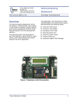
1
PCIS3BASE
V 1.3 June 29, 2010
User Manual C1010-3105
SPARTAN-3 FPGA board with PCI interface
Order number: C1010-3105
PCIS3BASE / C1010-3105
User Doc V1.3
http://www.cesys.com/
-1-
preliminary
Copyright information
Copyright © 2010 CESYS GmbH. All Rights Reserved. The information in this document is
proprietary to CESYS GmbH. No part of this document may be reproduced in any form or
by any means or used to make derivative work (such as translation, transformation or
adaptation) without written permission from CESYS GmbH.
CESYS GmbH provides this documentation without warranty, term or condition of any kind,
either express or implied, including, but not limited to, express and implied warranties of
merchantability, fitness for a particular purpose, and non-infringement. While the
information contained herein is believed to be accurate, such information is preliminary,
and no representations or warranties of accuracy or completeness are made. In no event
will CESYS GmbH be liable for damages arising directly or indirectly from any use of or
reliance upon the information contained in this document. CESYS GmbH will make
improvements or changes in the product(s) and/or program(s) described in this
documentation at any time.
CESYS GmbH retains the right to make changes to this product at any time, without notice.
Products may have minor variations to this publication, known as errata. CESYS GmbH
assumes no liability whatsoever, including infringement of any patent or copyright, for sale
and use of CESYS GmbH products.
CESYS GmbH and the CESYS logo are registered trademarks.
All product names are trademarks, registered trademarks, or service marks of their
respective owner.
⇒ Please check www.cesys.com to get the latest version of this document.
CESYS Gesellschaft für angewandte Mikroelektronik mbH
Zeppelinstrasse 6a
D – 91074 Herzogenaurach
Germany
PCIS3BASE / C1010-3105
User Doc V1.3
http://www.cesys.com/
-2-
preliminary
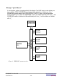
Overview
Summary of PCIS3BASE
The PCIS3BASE board is designed to meet today’s demands on development speed and
flexibility. Its heart is a 1,5 Million gates Spartan-3 FPGA. The master-clock and 93 FPGA
I/O Balls are routed to the expansion connector of the plug-in-board (PIB) slot. The PIB slot
also has connections to a 78-pin HD-SUB I/O connector. Plug-in boards can be standard
boards from CESYS, a board carrying the functionality defined by you or even your own
board.
• The standard plug-in board that comes with PCIS3BASE, provides 64 signals with 5 Volt
tolerant buffers.
• Plug-in boards can carry various interfaces like ADC, DAC, TTL Level I/O, RS232,
RS485, LVDS, Camera Link or user-defined interface standards.
• In addition to the Spartan-3 FPGA, there are 32 MByte SDRAM, Serial Flash Memory, an
internal interface and a bus-master PCI bridge on board.
• Users who wish to develop their own PCI-boards based on the PCIS3BASE can
purchase the PCIS3BASE source code package which contains the schematics of the
board as well all all sources (API, Tools).
• The PCI interface is not implemented inside the FPGA. There is a dedicated PCI-bridge
chip on the board. The FPGA connects to its local bus. This local bus is much easier to
handle than PCI. VHDL sample code that demonstrates how to use it comes with the
PCIS3BASE. Therefore, designers need not care about PCI-specific details. No PCI IPcore is needed.
Feature list
•
•
•
•
•
•
•
•
•
•
•
•
XILINX Spartan-3 FPGA 1.5 MIO system gates (XC3S1500-4FGG456C)
PCI host bridge supports 3,3 Volt and 5 Volt PCI (PLX PCI9056BA66)
High performance, up to 120 MByte/s data rate on PCI bus possible
32 MByte SDRAM (MICRON 48LC16M16A2)
SPI Serial Flash Memory 4 MBit (512 KBytes x 8)
PCI 2.1 compliant device (Plug-and-Play)
78-pin external I/O connector
PIB64IO board included (64 I/O signals on ext. I/O connector, 5 Volt TTL)
Allocated space for plug-in-board with two 100 pin connectors
Internal expansion port RM 2,54 mm (28 I/O pins)
8 Leds connected to the FPGA
JTAG connector for debugging and configuration
PCIS3BASE / C1010-3105
User Doc V1.3
http://www.cesys.com/
-3-
preliminary
Included in delivery
•
•
•
•
PCIS3BASE board
PIB64IO plug-in-board
One mating SUB-D high density 78-pin connector
One CD-ROM containing the user's manual (English), drivers, libraries, tools and
example source code.
The included software, demonstration code and documentations might not be used without
a CESYS PCIS3BASE board nor distributed isolated.
The complete schematics of the board together with the software source-code of the API
and a license to use the CESYS API and software separately from the PCIS3BASE board
is available to customers who wish to take the PCIS3BASE as a starting point for
developing their own products. (order number C 2070 – 3706, PCIS3BASE source code
package). The source code package includes the right to use and distribute the software
and code examples without the original CESYS PCIS3BASE boards.
PCIS3BASE / C1010-3105
User Doc V1.3
http://www.cesys.com/
-4-
preliminary
Hardware
Internal
Expansion
HD-SUB 78
Plug-In board
C
o
n
n
e
c
t
o
r
C
o
n
n
e
c
t
o
r
JTAG
FPGA
SPARTAN-3
XC3S1500
Local
Bus
4 MBit SPI
Flash Memory
32 MByte
SDRAM
50MHz
Leds
PCI9056
PCI
Bus bridge
PCI Bus
Figure 1: PCIS3BASE block diagram
SPARTAN-3 FPGA
XC3S1500-4FGG456C FPGA features:
System Gates
1500k
Configurable Logic Blocks
64 x 52
Logic cells
29,952
Block Ram Bits
576k
Distributed Ram Bits
208k
DCMs
4
Multipliers
32
For details on SPARTAN-3TM FPGA, please refer to data sheet at:
http://direct.xilinx.com/bvdocs/publications/ds099.pdf
PCIS3BASE / C1010-3105
User Doc V1.3
http://www.cesys.com/
-5-
preliminary
CESYS PIB slot
Like some other CESYS boards, PCIS3BASE has a Plug-In Board slot. The PIB slot
consists of two 100-pin connectors. One is wired to FPGA I/O balls, the other is wired to an
external 78-pin HD-Sub connector. To enable active devices to be powered on usergenerated PIB modules, supply voltages +3,3 Volt, +5 Volt and +12V are also available.
Delivered as standard with PCIS3BASE comes the PIB module PIB64IO with 64 IO (8
ports à 8 IO) with 5V tolerant buffers. For further information on pinout and switching
characteristics please check PIB64IO documentation.
4x 3.2
v1.0
P IB64IO
side of P lug-in board
C onnectors are
3.24
70.85
9.89
73.01
76.25
7.5
16.5
located on bottom
TOP
26.5
33.5
50
[mm]
64
Figure 2: PIB outline drawing and dimensions
PCIS3BASE / C1010-3105
User Doc V1.3
http://www.cesys.com/
-6-
preliminary
Board Size
PCIS3BASE complies to PCI Local Bus Specification Revision 2.3 as Universal 32-bit
short-card and supports both 3,3 Volt and 5V signaling.
7 7 .0 5
3 6 .0 5
33 .5
1 0 4 .7 7
1 0 8 .2 5
2 7.0 5
O3.2 x6
35
26 .5
14
33
13 9
Figure 3: PCIS3BASE outline and dimensions
PCIS3BASE / C1010-3105
User Doc V1.3
http://www.cesys.com/
-7-
preliminary
Connectors and FPGA pinout
1
100
1
J21
100
XIL INX
CO N 7
CO N 8
PIB
m o d u le
SP ART AN-3
FPGA
CON9
s lo t
SD RAM
CO N 1
50
50
51
51
PL X
L ED_G
9 056
Y1
L ED_Y
C 1 01 0-3 1 05
Figure 4: PCIS3BASE connector diagram
Description
PCIS3BASE can be used as a development platform for designs with XILINIX TM SPARTAN3 FPGAs as well as an OEM-component for job lot production. A 78-pin high-density DSUB connector allows the attachment of external hardware to the FPGA. Between 78-pin
connector and FPGA IO-pins, there is allocated space with two 100-pin connectors to plug
user-interface electronics (PIB). The PCIS3BASE board comes with a PIB that provides
5Volt tolerant IOs organized in 8 signals by 8 banks (PIB64IO). The board is equipped with
a XC3S1500-4FGG456C XILINXTM FPGA, a member of the Spartan-3 family. This
programmable logic device is configured by loading a bitstream that represents the design.
The software that comes with the board permits to load new configurations at any time.
There is no need to reboot the computer. Because the PCI interface is implemented by
using the dedicated PCI-bridge chip PCI9056 from PLX Technology TM, the user does not
need to bother about PCI bus implementation details nor has to use PCI cores in his FPGA
design. A 50 MHz clock oscillator supplies the basic clock that can be used by the FPGA.
Additional clock sources can be present on PIBs if required.
PCIS3BASE / C1010-3105
User Doc V1.3
http://www.cesys.com/
-8-
preliminary
FPGA I/O balls
All FPGA VCCO-Pins on PCIS3BASE board are connected to 3,3 Volt. The I/O Balls of the
SPARTAN-3 FPGA do NOT accept 5 Volt Input signals. If 5 Volt signals are connected
without proper level-shifting or series resistors, the FPGA will get damaged. If 3,3 Volt
signals are used with long traces or cables in conjunction with improper termination, the
resulting overshoot and undershoot may damage the FPGA as well. Please refer to
XilinxTM application note xapp659.pdf for details.
! Never apply voltages outside the interval [-0.5V….+3.8V] to any FPGA I/O Ball. Take care
of overshoot / undershoot conditions.
Please use the File “pcis3base.ucf” when assigning FPGA I/O balls to your design.
Although the ball positions in this documentation are double-checked, the ucf-file is the
more reliable source.
LEDs
Figure 5: PCIS3BASE slot bracket
The PCIS3BASE is equipped with several LEDs. Upon successful configuration the CFG
LED lights up and stays on as long as the device is configured. Additionally 8 userconfigurable LEDs allow to make internal monitoring states visible by driving the
appropriate FPGA I/O high.
LEDs
LED
LED1 Green
LED2 Green
LED3 Green
LED4 Green
LED5 Yellow
LED6 Yellow
LED7 Yellow
LED8 Yellow
CFG LED
Comment
FPGA I/O Ball U2
FPGA I/O Ball U3
FPGA I/O Ball U4
FPGA I/O Ball U5
FPGA I/O Ball V1
FPGA I/O Ball V2
FPGA I/O Ball V3
FPGA I/O Ball V4
Configuration LED
PCIS3BASE / C1010-3105
User Doc V1.3
http://www.cesys.com/
-9-
preliminary
Plug-In board connectors
The two 100-pin external expansion connectors are of type “female” with 1,27mm pitch (2
rows, 50 pins each). Please use the connector diagram to indicate pin 1. Mating
connectors among others are:
• SELTRONICS:
• SAMTEC:
order number: PL 169-35-100-G
order number: TFM-150-02-SDA
CON7 is used to connect the PIB to the FPGA
CON 7
Plug-In board to FPGA I/O- pin connector
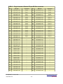
Pin
Signal name
FPGA I/O ball
Pin
Signal name
FPGA I/O ball
1
PIB_IO 0
A14
100
PIB_IO 92
C6
2
PIB_IO 1
B14
99
PIB_IO 91
C5
3
PIB_IO 2
D14
98
PIB_IO 90
C2
4
GND
--
97
PIB_IO 89
C1
5
PIB_IO 3
E14
96
PIB_IO 88
D6
6
PIB_IO 4
A13
95
PIB_IO 87
D5
7
PIB_IO 5
B13
94
PIB_IO 86
D4
8
PIB_IO 6
C13
93
PIB_IO 85
D3
9
PIB_IO 7
D13
92
PIB_IO 84
D2
10
PIB_IO 8
E13
91
PIB_IO 83
D1
11
PIB_IO 9
F13
90
PIB_IO 82
E6
12
PIB_IO 10
A12
89
PIB_IO 81
E4
13
PIB_IO 11
B12 (GCLK5)
88
PIB_IO 80
E3
14
PIB_IO 12
C12 (GCLK4)
87
PIB_IO 79
E2
15
PIB_IO 13
D12
86
PIB_IO 78
E1
16
PIB_IO 14
E12
85
PIB_IO 77
F6
17
PIB_IO 15
F12
84
PIB_IO 76
F5
18
PIB_IO 16
A11 (GCLK6)
83
PIB_IO 75
F4
19
PIB_IO 17
B11 (GCLK7)
82
PIB_IO 74
F3
20
PIB_IO 18
C11
81
PIB_IO 73
F2
21
PIB_IO 19
D11
80
PIB_IO 72
G6
22
PIB_IO 20
E11
79
PIB_IO 71
G5
23
GND
--
78
PIB_IO 70
G2
24
PIB_IO 21
F11
77
PIB_IO 69
G1
25
PIB_IO 22
A10
76
PIB_IO 68
H5
PCIS3BASE / C1010-3105
User Doc V1.3
http://www.cesys.com/
-10-
preliminary
CON 7
Plug-In board to FPGA I/O- pin connector
Pin
Signal name
FPGA I/O ball
Pin
Signal name
FPGA I/O ball
26
PIB_IO 23
B10
75
PIB_IO 67
K4
27
PIB_IO 24
C10
74
PIB_IO 66
K3
28
PIB_IO 25
D10
73
PIB_IO 65
K2
29
PIB_IO 26
E10
72
PIB_IO 64
K1
30
PIB_IO 27
F10
71
PIB_IO 63
L6
31
PIB_IO 28
A9
70
PIB_IO 62
L5
32
PIB_IO 29
B9
69
PIB_IO 61
L4
33
PIB_IO 30
D9
68
PIB_IO 60
L3
34
PIB_IO 31
E9
67
PIB_IO 59
L2
35
PIB_IO 32
F9
66
PIB_IO 58
L1
36
PIB_IO 33
A8
65
PIB_IO 57
M1
37
PIB_IO 34
B8
64
PIB_IO 56
M2
38
PIB_IO 35
C7
63
PIB_IO 55
M3
39
PIB_IO 36
D7
62
PIB_IO 54
M4
40
PIB_IO 37
E7
61
PIB_IO 53
M5
41
PIB_IO 38
F7
60
PIB_IO 52
M6
42
PIB_IO 39
A5
59
PIB_IO 51
N1
43
PIB_IO 40
A3
58
PIB_IO 50
N2
44
PIBCLK (50MHz)
--
57
PIB_IO 49
N3
45
GND
--
56
PIB_IO 48
N4
46
PIB_IO 41
B5
55
PIB_IO 47
T1
47
PIB_IO 42
B6
54
PIB_IO 46
T2
48
+3,3 Volt
--
53
PIB_IO 45
T4
49
+3,3 Volt
--
52
PIB_IO 44
T5
50
+3,3 Volt
--
51
PIB_IO 43
T6
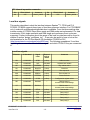
CON8 is used to connect the PIB to the HD-Sub connector CON9
CON 8
Plug-In board to External 78-pin HD-Sub connector
Pin
HD-Sub
Comment
Pin
HD-Sub
Comment
1
GND
--
100
GND
--
2
GND
--
99
GND
--
3
GND
--
98
GND
--
4
HD-Sub Pin 39
Pair 0
97
HD-Sub Pin 59
Pair 8
PCIS3BASE / C1010-3105
User Doc V1.3
http://www.cesys.com/
-11-
preliminary
CON 8
Plug-In board to External 78-pin HD-Sub connector
Pin
HD-Sub
Comment
Pin
HD-Sub
Comment
5
HD-Sub Pin 20
Pair 0
96
HD-Sub Pin 78
Pair 8
6
HD-Sub Pin 38
Pair 1
95
HD-Sub Pin 58
Pair 9
7
HD-Sub Pin 19
Pair 1
94
HD-Sub Pin 77
Pair 9
8
HD-Sub Pin 37
Pair 2
93
HD-Sub Pin 57
Pair 10
9
HD-Sub Pin 18
Pair 2
92
HD-Sub Pin 76
Pair 10
10
HD-Sub Pin 36
Pair 3
91
HD-Sub Pin 56
Pair 11
11
HD-Sub Pin 17
Pair 3
90
HD-Sub Pin 75
Pair 11
12
HD-Sub Pin 35
Pair 4
89
HD-Sub Pin 55
Pair 12
13
HD-Sub Pin 16
Pair 4
88
HD-Sub Pin 74
Pair 12
14
HD-Sub Pin 34
Pair 5
87
HD-Sub Pin 54
Pair 13
15
HD-Sub Pin 15
Pair 5
86
HD-Sub Pin 73
Pair 13
16
HD-Sub Pin 33
Pair 6
85
HD-Sub Pin 53
Pair 14
17
HD-Sub Pin 14
Pair 6
84
HD-Sub Pin 72
Pair 14
18
HD-Sub Pin 32
Pair 7
83
HD-Sub Pin 52
Pair 15
19
HD-Sub Pin 13
Pair 7
82
HD-Sub Pin 71
Pair 15
20
HD-Sub Pin 12
--
81
HD-Sub Pin 51
--
21
HD-Sub Pin 31
--
80
HD-Sub Pin 70
--
22
HD-Sub Pin 11
--
79
HD-Sub Pin 50
--
23
HD-Sub Pin 30
--
78
HD-Sub Pin 69
--
24
HD-Sub Pin 10
--
77
HD-Sub Pin 68
--
25
HD-Sub Pin 9
--
76
HD-Sub Pin 67
--
26
HD-Sub Pin 8
--
75
HD-Sub Pin 66
--
27
HD-Sub Pin 7
--
74
HD-Sub Pin 65
--
28
HD-Sub Pin 6
--
73
HD-Sub Pin 64
--
29
HD-Sub Pin 5
--
72
HD-Sub Pin 63
--
30
HD-Sub Pin 4
--
71
HD-Sub Pin 62
--
31
HD-Sub Pin 3
--
70
HD-Sub Pin 61
--
32
HD-Sub Pin 2
--
69
HD-Sub Pin 60
--
33
HD-Sub Pin 29
--
68
HD-Sub Pin 49
--
34
HD-Sub Pin 28
--
67
HD-Sub Pin 48
--
35
HD-Sub Pin 27
--
66
HD-Sub Pin 47
--
36
HD-Sub Pin 26
--
65
HD-Sub Pin 46
--
37
HD-Sub Pin 25
--
64
HD-Sub Pin 45
--
38
HD-Sub Pin 24
--
63
HD-Sub Pin 44
--
PCIS3BASE / C1010-3105
User Doc V1.3
http://www.cesys.com/
-12-
preliminary
CON 8
Plug-In board to External 78-pin HD-Sub connector
Pin
HD-Sub
Comment
Pin
HD-Sub
Comment
39
HD-Sub Pin 23
--
62
HD-Sub Pin 43
--
40
HD-Sub Pin 22
--
61
HD-Sub Pin 42
--
41
HD-Sub Pin 21
--
60
HD-Sub Pin 41
--
42
GND
--
59
GND
--
43
GND
--
58
GND
--
44
GND
--
57
GND
--
45
+5 Volt
--
56
+5 Volt
--
46
+5 Volt
--
55
+5 Volt
--
47
+5 Volt
--
54
+5 Volt
--
48
+12 Volt
--
53
+12 Volt
--
49
+12 Volt
--
52
+12 Volt
--
50
+12 Volt
--
51
+12 Volt
--
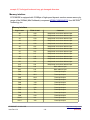
To simplify connections to the external HD-Sub connector CON9 the following table lists all
connections from HD-Sub to internal PIB- connector CON8.
HD-Sub
External 78-pin HD-Sub to Plug-In board connector CON 8
HD-SUB
PIB
HD-SUB
PIB
HD-SUB
PIB
HD-SUB
PIB
HD-Pin 1
GND
HD-Pin 21
41
HD-Pin 40
EARTH
HD-Pin 60
69
HD-Pin 2
32
HD-Pin 22
40
HD-Pin 41
60
HD-Pin 61
70
HD-Pin 3
31
HD-Pin 23
39
HD-Pin 42
61
HD-Pin 62
71
HD-Pin 4
30
HD-Pin 24
38
HD-Pin 43
62
HD-Pin 63
72
HD-Pin 5
29
HD-Pin 25
37
HD-Pin 44
63
HD-Pin 64
73
HD-Pin 6
28
HD-Pin 26
36
HD-Pin 45
64
HD-Pin 65
74
HD-Pin 7
27
HD-Pin 27
35
HD-Pin 46
65
HD-Pin 66
75
HD-Pin 8
26
HD-Pin 28
34
HD-Pin 47
66
HD-Pin 67
76
HD-Pin 9
25
HD-Pin 29
33
HD-Pin 48
67
HD-Pin 68
77
HD-Pin 10
24
HD-Pin 30
23
HD-Pin 49
68
HD-Pin 69
78
HD-Pin 11
22
HD-Pin 31
21
HD-Pin 50
79
HD-Pin 70
80
HD-Pin 12
20
HD-Pin 32
18
HD-Pin 51
81
HD-Pin 71
82
HD-Pin 13
19
HD-Pin 33
16
HD-Pin 52
83
HD-Pin 72
84
HD-Pin 14
17
HD-Pin 34
14
HD-Pin 53
85
HD-Pin 73
86
HD-Pin 15
15
HD-Pin 35
12
HD-Pin 54
87
HD-Pin 74
88
HD-Pin 16
13
HD-Pin 36
10
HD-Pin 55
89
HD-Pin 75
90
PCIS3BASE / C1010-3105
User Doc V1.3
http://www.cesys.com/
-13-
preliminary
HD-Sub
External 78-pin HD-Sub to Plug-In board connector CON 8
HD-SUB
PIB
HD-SUB
PIB
HD-SUB
PIB
HD-SUB
PIB
HD-Pin 17
11
HD-Pin 37
8
HD-Pin 56
91
HD-Pin 76
92
HD-Pin 18
9
HD-Pin 38
6
HD-Pin 57
93
HD-Pin 77
94
HD-Pin 19
7
HD-Pin 39
4
HD-Pin 58
95
HD-Pin 78
96
HD-Pin 20
5
--
--
HD-Pin 59
97
--
--
Internal Expansion port J21
The internal expansion connector J21 is of type male with 2,54 mm pitch (2 rows, 17 pins
each). The pins are connected to the FPGA directly. IO pins are NOT 5V tolerant.
! Never apply voltages outside the interval [-0.5V….+3.8V] to any FPGA I/O Ball. Take care
of overshoot / undershoot conditions.
Through J21 28 FPGA I/O are accessible. 24 of these I/O are routed as 12 pairs to support
differential signalling optionally. 3,3 Volt power supply is also available, so it is even
possible to power active devices on boards connected to J21. Current supplied over J21
should not exceed 100mA.
J21 Internal expansion connector
Pin
FPGA I/O ball
Comment
Pin
FPGA I/O ball
Comment
1
E21
Bank2_IO21N
2
E22
Bank2_IO21P
3
D21
Bank2_IO17N
4
D22
Bank2_IO17P
5
C22
--
6
F17
--
7
E19
Bank2_IO20N
8
E20
Bank2_IO20P
9
GND
--
10
GND
--
11
D19
Bank2_IO16P
12
D20
Bank2_IO16N
13
E18
Bank2_IO19N
14
F18
Bank2_IO19P
15
A19
Bank1_IO06N
16
B19
Bank1_IO06P
17
C18
Bank1_IO09N
18
D18
Bank1_IO09P
19
GND
--
20
GND
--
21
A18
Bank1_IO10N
22
B18
Bank1_IO10P
23
D17
Bank1_IO15N
24
E17
Bank1_IO15P
25
E16
--
26
F16
--
27
B17
Bank1_IO16P
28
C17
Bank1_IO16N
29
3,3 Volt
--
30
3,3 Volt
--
31
D15
Bank1_IO24N
32
E15
Bank1_IO24P
PCIS3BASE / C1010-3105
User Doc V1.3
http://www.cesys.com/
-14-
preliminary
J21 Internal expansion connector
Pin
FPGA I/O ball
Comment
Pin
FPGA I/O ball
Comment
33
A15
Bank1_IO25P
34
B15
Bank1_IO25N
Local bus signals
This section describes in short the interface between Spartan TM-3 FPGA and PLX
PCI9056. PCI9056 supports three types of local bus processor interface. For PCIS3BASE
only J mode with multiplexed address/data bus is available. From the three existing data
transfer modes of PCI9056 Direct Slave mode and DMA mode are implemented. For data
transmission 32-bit single read/write and DMA single and continuous burst cycles are
supported. Further information about the usage of the local bus interface can be found in
chapter D section 'design “pcis3base_top” '. It may also be useful to have a look at the
documentation for the PCI Bus Master I/O Accelerator PCI9056 at PLX
(http://www.plxtech.com/products/io/pci9056.asp). The following spreadsheet “Local bus
signals” gives an overview of the local bus signals and which FPGA I/O they are connected
to.
Local bus signals
FPGA I/O
I/O Standard
Signal
name
External
pull-up
/down
Comment
W4
LVCMOS33
ADS#
pull-up
Address strobe
Y18
LVCMOS33
ALE
pull-down
Address latch enable
W5
LVCMOS33
BIGEND#
pull-up
Big- endian select
W1
LVCMOS33
BLAST#
pull-up
Burst last
W2
LVCMOS33
BREQi
pull-down
Bus request in
AA6
LVCMOS33
BREQo
pull-up
Bus request out
U10
LVCMOS33
BTERM#
pull-up
Burst terminate
U6
LVCMOS33
CCS#
pull-up
Configuration register select
W6
LVCMOS33
DACK0#
--
DMA channel 0
demand mode acknowledge
U7
LVCMOS33
DACK1#
--
DMA channel 1
demand mode acknowledge
W18
LVCMOS33
DEN#
pull-up
Data enable
W9
LVCMOS33
DP0
pull-down
Data parity 0
Y1
LVCMOS33
DP1
pull-down
Data parity 1
AA8
LVCMOS33
DP2
pull-down
Data parity 2
V9
LVCMOS33
DP3
pull-down
Data parity 3
PCIS3BASE / C1010-3105
User Doc V1.3
http://www.cesys.com/
-15-
preliminary
Local bus signals
FPGA I/O
I/O Standard
Signal
name
External
pull-up
/down
Comment
Y5
LVCMOS33
DREQ0#
pull-up
DMA channel 0
demand mode request
V7
LVCMOS33
DREQ1#
pull-up
DMA channel 1
demand mode request
V18
LVCMOS33
DT/R#
pull-up
Data transmit / receive
AA4
LVCMOS33
EOT#
pull-up
End of transfer
for current DMA channel
AA14
LVCMOS33
LAD 0
pull-up
Multiplexed data address bus
AB14
LVCMOS33
LAD 1
pull-up
Multiplexed data address bus
U12
LVCMOS33
LAD 2
pull-up
Multiplexed data address bus
V12
LVCMOS33
LAD 3
pull-up
Multiplexed data address bus
W11
LVCMOS33
LAD 4
pull-up
Multiplexed data address bus
V11
LVCMOS33
LAD 5
pull-up
Multiplexed data address bus
AB9
LVCMOS33
LAD 6
pull-up
Multiplexed data address bus
AA9
LVCMOS33
LAD 7
pull-up
Multiplexed data address bus
Y10
LVCMOS33
LAD 8
pull-up
Multiplexed data address bus
V10
LVCMOS33
LAD 9
pull-up
Multiplexed data address bus
W10
LVCMOS33
LAD 10
pull-up
Multiplexed data address bus
AA10
LVCMOS33
LAD 11
pull-up
Multiplexed data address bus
V13
LVCMOS33
LAD 12
pull-up
Multiplexed data address bus
Y13
LVCMOS33
LAD 13
pull-up
Multiplexed data address bus
W13
LVCMOS33
LAD 14
pull-up
Multiplexed data address bus
AA13
LVCMOS33
LAD 15
pull-up
Multiplexed data address bus
U11
LVCMOS33
LAD 16
pull-up
Multiplexed data address bus
AB10
LVCMOS33
LAD 17
pull-up
Multiplexed data address bus
AB11
LVCMOS33
LAD 18
pull-up
Multiplexed data address bus
U13
LVCMOS33
LAD 19
pull-up
Multiplexed data address bus
AB15
LVCMOS33
LAD 20
pull-up
Multiplexed data address bus
AA15
LVCMOS33
LAD 21
pull-up
Multiplexed data address bus
W16
LVCMOS33
LAD 22
pull-up
Multiplexed data address bus
Y16
LVCMOS33
LAD 23
pull-up
Multiplexed data address bus
AB13
LVCMOS33
LAD 24
pull-up
Multiplexed data address bus
V14
LVCMOS33
LAD 25
pull-up
Multiplexed data address bus
W14
LVCMOS33
LAD 26
pull-up
Multiplexed data address bus
PCIS3BASE / C1010-3105
User Doc V1.3
http://www.cesys.com/
-16-
preliminary
Local bus signals
FPGA I/O
I/O Standard
Signal
name
External
pull-up
/down
Comment
U14
LVCMOS33
LAD 27
pull-up
Multiplexed data address bus
V16
LVCMOS33
LAD 28
pull-up
Multiplexed data address bus
U16
LVCMOS33
LAD 29
pull-up
Multiplexed data address bus
U17
LVCMOS33
LAD 30
pull-up
Multiplexed data address bus
AA17
LVCMOS33
LAD 31
pull-up
Multiplexed data address bus
V17
LVCMOS33
LBE0#
pull-up
Local byte enable 0
AA18
LVCMOS33
LBE1#
pull-up
Local byte enable 1
Y17
LVCMOS33
LBE2#
pull-up
Local byte enable 2
AB18
LVCMOS33
LBE3#
pull-up
Local byte enable 3
--
LVCMOS33
LCLK
--
Local processor clock (66MHz)
AB4
LVCMOS33
LHOLD
pull-down
Local hold request
W3
LVCMOS33
LHOLDA
pull-down
Local hold acknowledge
V6
LVCMOS33
LINTi#
pull-up
Local interrupt input
Y6
LVCMOS33
LINTo#
pull-up
Local interrupt output
V5
LVCMOS33
LRESET#
pull-up
Local bus reset
W8
LVCMOS33
LSERR#
pull-up
Local system error interrupt output
W17
LVCMOS33
LW/R#
pull-up
Local write/read
AB8
LVCMOS33
READY#
pull-up
Ready I/O
V8
LVCMOS33
WAIT#
pull-up
Wait I/O
This table is for reference only. The sample design, that comes with the board shows how
to use the local bus interface. Users who wish to implement their own local-bus interface
will need a detailed knowledge of the PCI9056 local bus implementation.
ADS#
Indicates a valid address and start of a new Bus access. ADS# asserts for the first clock of
the Bus access.
LCLK
Local clock input. Sourced by onboard 50MHz oscillator.
LHOLD
Asserted to request use of the Local Bus.
PCIS3BASE / C1010-3105
User Doc V1.3
http://www.cesys.com/
-17-
preliminary
LHOLDA
The external Local Bus Arbiter asserts LHOLDA when bus ownership is granted in
response to LHOLD. The Local Bus should not be granted to the PCI 9056, unless
requested by LHOLD.
LINTo#
Synchronous output that remains asserted as long as the interrupt is enabled and the
interrupt condition exists.
LW/R#
Asserted low for reads and high for writes.
READY#
A Local slave asserts READY# to indicate that Read data on the bus is valid or that a Write
Data transfer is complete. READY# input is not sampled until the internal Wait State
Counter(s) expires (WAIT# output de-asserted).
JTAG Interface
In addition to configuration via PCI, it is possible to download configuration data using a
JTAG interface. The PCIS3BASE is equipped as standard with a 2- row 14- pin connector
to plug in the Parallel Cable IV 1 from XilinxTM. The JTAG interface is not only suitable to
download designs for testing purposes but enables the user to check a running design by
the help of software tools provided by XilinxTM, for instance ChipScope2.
CON1
JTAG connector
Pin
Comment
Pin 1, 3, 5, 7, 9, 11, 13
GND
Pin 2
+2,5 Volt
Pin 4
TMS
Pin 6
TCK
Pin 8
TDO
Pin 10
TDI
Pin 12, 14
Not connected
Attention: Don’t connect JTAG adapters that use 3,3 Volt signalling. The FPGA only
1 Parallel Cable IV is not included
2 ChipScope is not included. A demo version is available at the Xilinx TM webpage.
(http://www.xilinx.com/ise/optional_prod/cspro.htm)
PCIS3BASE / C1010-3105
User Doc V1.3
http://www.cesys.com/
-18-
preliminary
accepts 2,5 Volt signal levels and may get damaged otherwise.
Memory interface
PCIS3BASE is equipped with 32 MByte of high-speed dynamic random access memory by
usage of the 256Mbit (4Mx16x4banks) component MT48LC16M16A2P-75 from MICRONTM
Technology, Inc.
Memory Interface
Signal name
FPGA I/O ball
Comment
A0
K20
Multiplexed row/column address input
A1
G22
Multiplexed row/column address input
A2
G19
Multiplexed row/column address input
A3
G17
Multiplexed row/column address input
A4
G18
Multiplexed row/column address input
A5
G21
Multiplexed row/column address input
A6
K19
Multiplexed row/column address input
A7
K21
Multiplexed row/column address input
A8
L17
Multiplexed row/column address input
A9
L19
Multiplexed row/column address input
A10
K22
Multiplexed row/column address input
A11
L21
Multiplexed row/column address input
A12
L22
Multiplexed row/column address input
BA0
L20
Bank address input
BA1
L18
Bank address input
DQ0
Y21
Data input/output
DQ1
W21
Data input/output
DQ2
W19
Data input/output
DQ3
V21
Data input/output
DQ4
V19
Data input/output
DQ5
U20
Data input/output
DQ6
U18
Data input/output
DQ7
T21
Data input/output
DQ8
T22
Data input/output
DQ9
U19
Data input/output
DQ10
U21
Data input/output
DQ11
V20
Data input/output
PCIS3BASE / C1010-3105
User Doc V1.3
http://www.cesys.com/
-19-
preliminary
Memory Interface
Signal name
FPGA I/O ball
Comment
DQ12
V22
Data input/output
DQ13
W20
Data input/output
DQ14
W22
Data input/output
DQ15
Y22
Data input/output
CS#
N19
Chip select input (registered LOW)
WE#
R18
Write enable (registered LOW)
CAS#
N22
Column address strobe (registered LOW)
RAS#
N20
Row address strobe (registered LOW)
CKE#
N21
Clock enable input (registered LOW)
Clock
Y11
SDRAM Clock input
DQMH
T17
Input/output data mask
DQML
T18
Input/output data mask
SPI Flash
In addition to 32MByte dynamic SDRAM, 4MBit nonvolatile memory in form of a SPI Flash
M25P40-VMN6P from STMicroelectronis are available. This flash memory is not intended
for storing FPGA configuration bitstreams (no connection to FPGA configuration logic is
available) but to give the user the opportunity to store board specific data directly onboard.
The following table gives information about IO usage:
4MBit SPI Flash M25P40
Signal name
FPGA I/O ball
Comment
FLASH_#CS
F20
Chip Select
FLASH_SO
F19
Serial Data Output
FLASH_SI
M22
Serial Data Input
FLASH_SCK
F21
Serial Clock
FLASH_#HOLD
--
Active-Low Hold signal,
4k7 pull-up- resistor to 3.3Volt
FLASH_#WP
--
Active-Low Write Protect signal,
4k7 pull-up- resistor to 3.3Volt
PCIS3BASE / C1010-3105
User Doc V1.3
http://www.cesys.com/
-20-
preliminary
FPGA design
Introduction
The PCIS3BASE-Board comes with the complete source code of two FPGA-designs. The
one, which demonstrates the implementation of a system-on-chip (SOC) with access to all
peripherals over PCI, is called “pcis3base”. The other one demonstrates high speed data
transfers from and to the FPGA over PCI and is called “performance_test”.
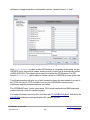
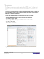
For own applications you will have to change some options of the project properties if you
want to download your FPGA design with the CESYS software API-functions LoadBIN()
and ProgramFPGA(). A bitstream in the “*.bin”-format is needed for downloading, but in
the ISE development environment the generation of this file is disabled by default. You will
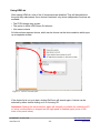
have to right click on process “generate programming file” then select properties=>general
options and check “create binary configuration file”:
Figure 6: ISE Generate Programming File Properties (Gen. Opt.)
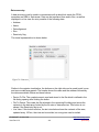
There are some control signals of the PLX PCI controller routed to FPGA pins, but not
used in FPGA designs. These signals must not be pulled into any direction! Therefore you
PCIS3BASE / C1010-3105
User Doc V1.3
http://www.cesys.com/
-21-
preliminary
will have to change properties=>configuration options “unused iob pins” to “float”:
Figure 7: ISE Generate Programming File Properties (Config. Opt.)
After ProgramFPGA() is called and the FPGA design is completely downloaded, the pin
LRESET# (note: the postfix # means, that the signal is active low) is automatically pulsed
(HIGH/LOW/HIGH). This signal can be used for resetting the FPGA design. The APIfunction ResetFPGA() can be called to initiate a pulse on LRESET# at a user given time.
The following sections will give you a brief introduction about the data transfer from and to
the FPGA over the PLX PCI controller local bus, the WISHBONE interconnection
architecture and the provided peripheral controllers.
The PCIS3BASE uses J mode, direct slave, 32-bit single read/write and DMA single and
continuous burst cycles for transferring data.
For further information about the PLX local bus see PCI 9056BA Data Book and about the
WISHBONE architecture see specification B.3 (wbspec_b3.pdf).
PCIS3BASE / C1010-3105
User Doc V1.3
http://www.cesys.com/
-22-
preliminary
FPGA source code copyright information
This source code is copyrighted by CESYS GmbH / GERMANY, unless otherwise noted.
FPGA source code license
THIS SOURCECODE IS NOT FREE! IT IS FOR USE TOGETHER WITH THE CESYS
PCIS3BASE PCI CARD ONLY! YOU ARE NOT ALLOWED TO MODIFY AND DISTRIBUTE
OR USE IT WITH ANY OTHER HARDWARE, SOFTWARE OR ANY OTHER KIND OF
ASIC OR PROGRAMMABLE LOGIC DESIGN WITHOUT THE EXPLICIT PERMISSION
OF THE COPYRIGHT HOLDER!
Disclaimer of warranty
THIS SOURCECODE IS DISTRIBUTED IN THE HOPE THAT IT WILL BE USEFUL, BUT
THERE IS NO WARRANTY OR SUPPORT FOR THIS SOURCECODE. THE COPYRIGHT
HOLDER PROVIDES THIS SOURCECODE "AS IS" WITHOUT WARRANTY OF ANY
KIND, EITHER EXPRESSED OR IMPLIED, INCLUDING, BUT NOT LIMITED TO, THE
IMPLIED WARRANTIES OF MERCHANTABILITY AND FITNESS FOR A PARTICULAR
PURPOSE. THE ENTIRE RISK AS TO THE QUALITY AND PERFORMANCE OF THIS
SOURCECODE IS WITH YOU. SHOULD THIS SOURCECODE PROVE DEFECTIVE,
YOU ASSUME THE COST OF ALL NECESSARY SERVICING, REPAIR OR
CORRECTION.
IN NO EVENT WILL THE COPYRIGHT HOLDER BE LIABLE TO YOU FOR DAMAGES,
INCLUDING ANY GENERAL, SPECIAL, INCIDENTAL OR CONSEQUENTIAL DAMAGES
ARISING OUT OF THE USE OR INABILITY TO USE THIS SOURCECODE (INCLUDING
BUT NOT LIMITED TO LOSS OF DATA OR DATA BEING RENDERED INACCURATE OR
LOSSES SUSTAINED BY YOU OR THIRD PARTIES OR A FAILURE OF THIS
SOURCECODE TO OPERATE WITH ANY OTHER SOFTWARE-PROGRAMS,
HARDWARE-CIRCUITS OR ANY OTHER KIND OF ASIC OR PROGRAMMABLE LOGIC
DESIGN), EVEN IF THE COPYRIGHT HOLDER HAS BEEN ADVISED OF THE
POSSIBILITY OF SUCH DAMAGES.
PCIS3BASE / C1010-3105
User Doc V1.3
http://www.cesys.com/
-23-
preliminary
Design “pcis3base”
An on-chip-bus system is implemented in this design. The VHDL source code shows you,
how to build a 32-Bit WISHBONE based shared bus architecture. All devices of the
WISHBONE system support only SINGLE READ / WRITE Cycles. Files and modules
having something to do with the WISHBONE system are labeled with the prefix “wb_”. The
WISHBONE master is labeled with the additional prefix “ma_” and the slaves are labeled
with “sl_”.
SYSCON
MASTER:
PLX
INTERCON
SLAVE:
SDRAM
SLAVE:
FLASH
SLAVE:
GPIO
SLAVE:
TIMER
Figure 8: WISHBONE system overview
PCIS3BASE / C1010-3105
User Doc V1.3
http://www.cesys.com/
-24-
preliminary
Files and modules
src/wishbone.vhd:
A package containing datatypes, constants, components, signals and information for
software developers needed for the WISHBONE system. You will find C/C++-style
“#define”s with important addresses and values to copy and paste into your software
source code after VHDL comments (“- -”).
src/pcis3base_top.vhd:
This is the top level entity of the design. The WISHBONE components are instantiated
here. The internal VHDL signals are mapped to the 100 pin connector of the general
purpose I/O plug in boards, so the pinout of the user constraints file does not need to be
changed for other plug in boards. You will find a table with the column “HDL Pin” and some
pin explanations in the plug in board documentation at the end of this document. This table
associates the pin numbers of the FPGA and the 100 pin connector with the bidirectional
VHDL data bus port “pin_gpiomoduleport_io”.
src/wb_syscon.vhd:
This entity is a wrapper for BUFG_CLK0_FB_SUBM.vhd and provides the WISHBONE
system signals RST and CLK and the external SDRAM clock. It uses LRESET# and
SYSTEMCLOCK as external reset and clock source.
src/wb_intercon.vhd:
All WISHBONE devices are connected to this shared bus interconnection logic. Some
MSBs of the address are used to select the appropriate slave.
src/wb_ma_plx.vhd:
This is the entity of the WISHBONE master, which converts the local bus protocol for 32-Bit
single read/write-cycles of the PLX PCI controller into a WISHBONE conform one.
src/wb_sl_sdr.vhd:
The module encapsulates the low level SDRAM controller sdr_ctrl.vhd. The integrated
command register supports NOP, PRECHARGE, LOAD MODE REGISTER and NORMAL
OPERATION commands for SDRAM initialization. Please see the software code samples
and Micron SDRAM datasheet (256MSDRAM.pdf) for details on SDRAM initialization. The
integrated timer starts the AUTO REFRESH cycles automatically.
src/wb_sl_flash.vhd:
The module encapsulates the low level FLASH controller flash_ctrl.vhd. The integrated
PCIS3BASE / C1010-3105
User Doc V1.3
http://www.cesys.com/
-25-
preliminary
command register supports the BULK ERASE command, which erases the whole memory
by programming all bits to '1'. In write cycles the bit values can only be changed from '1' to
'0'. That means, that it is not allowed to have a write access to the same address twice
without erasing the whole flash before. The read access is as simple as reading from any
other WISHBONE device. Please see the SPI-FLASH data sheet (m25p40.pdf) for details
on programming and erasing.
src/wb_sl_gpio.vhd:
This entity shows you, how to control the dual 8-bit bus transceiver circuits (see
74FCT162245T_Datasheet.pdf for details) on the plug in board and use them as general
purpose I/Os. The four LEDs and the 28 bidirectional I/Os at the internal 34-pin connector
are controlled by this module as well.
src/wb_sl_timer.vhd:
A 32-bit timer with programmable period (20 ns steps). The timer starts running if the
period is not null. It generates an interrupt at overflow time. The interrupt output is asserted
as long as the interrupt is not acknowledged.
src/sdr_ctrl.vhd:
The low level SDRAM controller for the 32MB/16-bit SDRAM. It handles the basic timing
for the SDRAM commands. It works at 50 MHz with a fixed burst length of two and uses
AUTO PRECHARGE functionality.
src/flash_ctrl.vhd:
The low level FLASH controller for the 4MBit SPI FLASH memory. It supports reading and
writing of four bytes of data at one time as well as erasing the whole memory.
src/BUFG_CLK0_FB_SUBM.vhd :
A module with two SPARTAN-3 DCMs for external and internal clock deskew taken from
XILINX application note 462 “Using Digital Clock Managers (DCMs) in Spartan-3 FPGAs”
(see xapp462.pdf, xapp462_vhdl.zip).
pcis3base.ise:
Project file for Xilinx ISE version 8.2.03i.
pcis3base.ucf:
User constraint file with timing and pinout constraints.
PCIS3BASE / C1010-3105
User Doc V1.3
http://www.cesys.com/
-26-
preliminary
Module-hierarchy
Package wishbone
Entity pcis3base_top
Entity wb_syscon
Entity BUFG_CLK0_FB_SUBM
Entity wb_intercon
Entity wb_ma_plx
Entity wb_sl_sdr
Entity sdr_ctrl
Entity wb_sl_flash
Entity flash_ctrl
Entity wb_sl_gpio
Entity wb_sl_timer
Bus transactions
The API-functions ReadRegister(), WriteRegister() lead to direct slave single
cycles and ReadBlock(), WriteBlock() to DMA transfers. Bursting is not allowed in
the WISHBONE demo application. You can find details on enabling/disabling the local bus
continuous burst mode in the software API and the source code of the software examples.
There is no difference in the PLX local bus cycles “direct slave” and “DMA”, if continuous
burst is disabled for DMA transfers. The address is incremented automatically in block
transfers.
Local bus signals driven by the PLX PCI controller:
• LW/R#: local bus write/not read, indicates, if a read or write cycle is in progress
• ADS#: address strobe, indicates a valid address, if asserted low by PLX
Local bus signals driven by the FPGA:
• READY#: handshake signal, FPGA indicates a successful data transfer for writing and
valid data on bus for reading by asserting this signal low, FPGA can insert wait states by
delaying this signal
PCIS3BASE / C1010-3105
User Doc V1.3
http://www.cesys.com/
-27-
preliminary
Local bus signal driven by the PLX PCI controller and the FPGA:
• LAD[31:0]: 32-bit multiplexed address/data bus, FPGA drives valid data on this bus in
read cycles while asserting the READY# signal low, the FPGA LAD[31:0] output drivers
have to be in a high impedance state at all other times
ADS#
FPGA drives LAD[31:0]
LAD[31:0]
A
D
READY#
STB_O
WE_O
ADR_O[31:0]
A>>2
A>>2
DAT_O[31:0]
D
DAT_I[31:0]
ACK_I
WISHBONE MASTER
LW/R#
PLX Local Bus
CLK
Figure 9: Bus transactions with ReadRegister() and ReadBlock()
The PLX local bus protocol is converted into a WISHBONE based one. So the PLX
becomes a master device in the internal WISHBONE architecture. Input signals for the
WISHBONE master are labeled with the postfix “_I”, output signals with “_O”.
WISHBONE signals driven by the master:
• STB_O: strobe, qualifier for the other output signals of the master, indicates valid data
and control signals
• WE_O: write enable, indicates, if a write or read cycle is in progress
• ADR_O[31:0]: 32-bit address bus, the PLX local bus uses BYTE addressing, but the
WISHBONE system uses DWORD (32-Bit) addressing. The address is shifted two bits
inside the WISHBONE master module
• DAT_O[31:0]: 32-bit data out bus for data transportation from master to slaves
PCIS3BASE / C1010-3105
User Doc V1.3
http://www.cesys.com/
-28-
preliminary
WISHBONE signals driven by slaves:
• DAT_I[31:0]: 32-bit data in bus for data transportation from slaves to master
• ACK_I: handshake signal, slave devices indicate a successful data transfer for writing
and valid data on bus for reading by asserting this signal, slaves can insert wait states by
delaying this signal, this delay leads to a delay of the READY# signal on the local bus
side
The signals LHOLD (local hold request) driven by PLX and LHOLDA (local hold
acknowledge) driven by the FPGA are used for local bus arbitration. LHOLD can be simply
looped back to LHOLDA, because the PLX PCI controller is the one and only master on
the local bus.
LW/R#
ADS#
LAD[31:0]
A
D
D
READY#
STB_O
WE_O
ADR_O[31:0]
A>>2
A>>2
DAT_O[31:0]
D
D
DAT_I[31:0]
ACK_I
WISHBONE MASTER PLX Local Bus
CLK
Figure 10: Bus transactions with WriteRegister() and WriteBlock()
The WISHBONE signals in these illustrations and explanations are shown as simple bit
types or bit vector types, but in the VHDL code these signals could be encapsulated in
extended data types like arrays or records.
Example:
...
port map
(
...
ACK_I => intercon.masters.slave(2).ack,
PCIS3BASE / C1010-3105
User Doc V1.3
http://www.cesys.com/
-29-
preliminary
...
Port ACK_I is connected to signal ack of element 2 of array slave, of record masters, of
record intercon.
PCI interrupt
The FPGA has the possibility to cause PCI interrupts. The interrupt state can be checked
by calling the API-function WaitForInterrupt(). If the FPGA asserts the LINTi# (local
interrupt input) signal low, then the function returns immediately else it returns after the
programmed timeout period. The return value shows you if an interrupt event has been
occurred or not. The software has to acknowledge an interrupt, i. e. by writing to a special
address. The FPGA deasserts the LINTi# pin after recognizing the acknowledgment. The
interrupt functionality is demonstrated by the slave timer module.
PCIS3BASE / C1010-3105
User Doc V1.3
http://www.cesys.com/
-30-
preliminary
Design “performance_test”
Small and simple design to achieve maximum data rates over PCI.
!!!Attention!!! Do not drive any pins of the internal 34 pol. expansion connector J21 while
this design is loaded! The FPGA could be damaged because these pins are driven by
FPGA! Remove everything but measurement devices like oscilloscopes or logic analyzers!
The important local bus handshake signals are routed to the internal connector to give you
an idea, how the bus protocol works.
34 pol. internal expansion connector (J21)
Pin 1
RST
Pin 2
CLK
Pin 3
LHOLD
Pin 4
LHOLDA
Pin 5
ADS#
Pin 6
BLAST#
Pin 7
READY#
Pin 8
LW/R#
Files and modules
src/performance_test.vhd:
The module handles the local bus protocol as fast as possible and buffers the last value
transferred to the FPGA.
performance_test.ise:
Project file for Xilinx ISE version 8.2.03i.
performance_test.ucf:
User constraint file with timing and pinout constraints.
PCIS3BASE / C1010-3105
User Doc V1.3
http://www.cesys.com/
-31-
preliminary
Bus transactions
LW/R#
ADS#
BLAST#
LAD[31:0]
A
D0
D1
D2
Dn-1 Dn
PLX => FPGA
CLK
READY#
LW/R#
ADS#
BLAST#
FPGA drives LAD[31:0]
LAD[31:0]
A
D0
D1
Dn-1 Dn
FPGA => PLX
CLK
READY#
Figure 11: Bus transactions with ReadBlock() and WriteBlock() in continous burst mode
This design supports the local bus continuous burst transfers as well as the single cycle
transfers. For burst transfers the additional signal BLAST# (burst last) is needed, which is
driven by the PLX PCI controller. If this signal is asserted low, the PLX indicates the last
LWORD it wants to transmit or receive. The FPGA can use the READY# signal for inserting
wait states like in the single cycle mode. Furthermore the FPGA can drive the additional
signal BTERM# (burst terminate) to break the current burst transfer and request a new
address cycle. Note that the use of BTERM# is not demonstrated in “performance_test”,
because it would decrease the performance.
PCIS3BASE / C1010-3105
User Doc V1.3
http://www.cesys.com/
-32-
preliminary
Software
Introduction
The UDK (Unified Development Kit) is used to allow developers to communicate with
Cesys's USB and PCI(e) devices. Older releases were just a release of USB and PCI
drivers plus API combined with some shared code components. The latest UDK combines
all components into one single C++ project and offers interfaces to C++, C and for .NET
(Windows only). The API has functions to mask-able enumeration, unique device
identification (runtime), FPGA programming and 32bit bus based data communication. PCI
devices have additional support for interrupts.
Changes to previous versions
Beginning with release 2.0, the UDK API is a truly combined interface to Cesys's USB and
PCI devices. The class interface from the former USBUni and PCIBase API's was saved at
a large extend, so porting applications from previous UDK releases can be done without
much work.
Here are some notes about additional changes:
Complete rewrite
Build system cleanup, all UDK parts (except .NET) are now part of one large project
64 bit operating system support
UDK tools combined into one application (UDKLab)
Updated to latest PLX SDK (6.31)
Identical C, C++ and .NET API interface (.NET ⇒ Windows only)
Different versions of components collapsed to one UDK version
Windows only:
• Microsoft Windows Vista / Seven(7) support (PCI drivers are not released for Seven at
the moment)
• Driver installation / update is done by an installer now
• Switched to Microsoft's generic USB driver (WinUSB)
• Support moved to Visual Studio 2005, 2008 and 2010(experimental), older Visual
Studio versions are not supported anymore
• Linux only:
• Revisited USB driver, tested on latest Ubuntu distributions (32/64)
• Simpler USB driver installation
•
•
•
•
•
•
•
•
PCIS3BASE / C1010-3105
User Doc V1.3
http://www.cesys.com/
-33-
preliminary
Windows
Requirements
To use the UDK in own projects, the following is required:
•
•
•
•
Installed drivers
Microsoft Visual Studio 2005 or 2008; 2010 is experimental
CMake 2.6 or higher ⇒ http://www.cmake.org
wxWidgets 2.8.10 or higher (must be build separately) ⇒ http://www.wxwidgets.org
[optionally, only if UDKLab should be build]
Driver installation
The driver installation is part of the UDK installation but can run standalone on final
customer machines without the need to install the UDK itself. During installation, a choice
of drivers to install can be made, so it is not necessary to install i.e. PCI drivers on
machines that should run USB devices only or vice versa. If USB drivers get installed on a
machine that has a pre-2.0 UDK driver installation, we prefer the option for USB driver
cleanup offered by the installer, this cleanly removes all dependencies of the old driver
installation.
Note: There are separate installers for 32 and 64 bit systems.
Important: At least one device should be present when installing the drivers !
Build UDK
Prerequisites
The most components of the UDK are part of one large CMake project. There are some
options that need to be fixed in msvc.cmake inside the UDK installation root:
• BUILD_UI_TOOLS If 0, UDKLab will not be part of the subsequent build procedure, if 1 it
will. This requires an installation of an already built wxWidgets.
• WX_WIDGETS_BASE_PATH Path to wxWidgets build root, only needed if
BUILD_UI_TOOLS is not 0.
• USE_STATIC_RTL If 0, all projects are build against the dynamic runtime libraries. This
requires the installation of the appropriate Visual Studio redistributable pack on every
machine the UDK is used on. Using a static build does not create such dependencies,
but will conflict with the standard wxWidgets build configuration.
Solution creation and build
The preferred way is to open a command prompt inside the installation root of the UDK,
PCIS3BASE / C1010-3105
User Doc V1.3
http://www.cesys.com/
-34-
preliminary
lets assume to use c:\\udkapi.
c:
cd \udkapi
CMake allows the build directory separated to the source directory, so it's a good idea to do
it inside an empty sub-directory:
mkdir build
cd build
The following code requires an installation of CMake and at least one supported Visual
Studio version. If CMake isn't included into the PATH environment variable, the path must
be specified as well:
cmake ..
This searches the preferred Visual Studio installation and creates projects for it. Visual
Studio Express users may need to use the command prompt offered by their installation. If
multiple Visual Studio versions are installed, CMake's command parameter '-G' can be
used to specify a special one, see CMake's documentation in this case. This process
creates the solution files inside c:\\udkapi\\build. All subsequent tasks can be done in Visual
Studio (with the created solution), another invocation of cmake isn't necessary under
normal circumstances.
Important: The UDK C++ API must be build with the same toolchain and build flags like
the application that uses it. Otherwise unwanted side effects in exception handling will
occur ! (See example in Add project to UDK build).
Info: It is easy to create different builds with different Visual Studio versions by creating
different build directories and invoke CMake with different '-G' options inside them:
c:
cd \udkapi
mkdir build2005
cd build2005
cmake -G"Visual Studio 8 2005" ..
cd ..
mkdir build2008
cd build2008
cmake -G"Visual Studio 9 2008" ..
PCIS3BASE / C1010-3105
User Doc V1.3
http://www.cesys.com/
-35-
preliminary
Linux
There are too many distributions and releases to offer a unique way to the UDK installation.
We've chosen to work with the most recent Ubuntu release, 9.10 at the moment. All
commands are tested on an up to date installation and may need some tweaking on other
systems / versions.
Requirements
•
•
•
•
GNU C++ compiler toolchain
zlib development libraries
CMake 2.6 or higher ⇒ http://www.cmake.org
wxWidgets 2.8.10 or higher ⇒ http://www.wxwidgets.org [optionally, only if UDKLab
should be build]
sudo apt-get install build-essential cmake zlib1g-dev libwxbase2.8-dev
libwxgtk2.8-dev
The Linux UDK comes as gzip'ed tar archive, as the Windows installer won't usually work.
The best way is to extract it to the home directory:
tar xzvf UDKAPI-x.x.tgz ~/
This creates a directory /home/[user]/udkapi[version] which is subsequently called udkroot.
The following examples assume an installation root in ~/udkapi2.0.
Important: Commands sometimes contain a ` symbol, have attention to use the right one,
refer to command substitution if not familiar with.
Drivers
The driver installation on Linux systems is a bit more complicated than on Windows
systems. The drivers must be build against the installed kernel version. Updating the kernel
requires a rebuild.
USB
As the USB driver is written by Cesys, the installation procedure is designed to be as
simple and automated as possible. The sources and support files reside in directory
<udkroot>/drivers/linux/usb. Just go there and invoke make.
cd ~/udkapi2.0/drivers/linux/usb
make
If all external dependencies are met, the build procedure should finish without errors.
Newer kernel releases may change things which prevent success, but it is out of the scope
of our possibilities to be always up-to-date with latest kernels. To install the driver, the
PCIS3BASE / C1010-3105
User Doc V1.3
http://www.cesys.com/
-36-
preliminary
following command has to be done:
sudo make install
This will do the following things:
• Install the kernel module inside the module library path, update module dependencies
• Install a new udev rule to give device nodes the correct access rights (0666)
(/etc/udev/rules.d/99-ceusbuni.rules)
• Install module configuration file (/etc/dev/modprobe.d/ceusbuni.conf)
• Start module
If things work as intended, there must be an entry /proc/ceusbuni after this procedure.
The following code will completely revert the above installation (called in same directory):
sudo make remove
The configuration file, /etc/modprobe.d/ceusbuni.conf, offers two simple options (Read the
comments in the file):
• Enable kernel module debugging
• Choose between firmware which automatically powers board peripherals or not
Changing these options require a module reload to take affect.
PCI
The PCI drivers are not created or maintained by Cesys, they are offered by the
manufacturer of the PCI bridges that were used on Cesys PCI(e) boards. So problems
regarding them can't be handled or supported by us.
Important: If building PlxSdk components generate the following error / warning:
/bin/sh [[: not found
Here's a workaround: The problem is Ubuntu's default usage of dash as sh, which can't
handle command [[. Replacing dash with bash is accomplished by the following commands
that must be done as root:
sudo rm /bin/sh
sudo ln -s /bin/bash /bin/sh
Installation explained in detail:
PlxSdk decompression:
cd ~/udkapi2.0/drivers/linux
tar xvf PlxSdk.tar
PCIS3BASE / C1010-3105
User Doc V1.3
http://www.cesys.com/
-37-
preliminary
Build drivers:
cd PlxSdk/Linux/Driver
PLX_SDK_DIR=`pwd`/../../ ./buildalldrivers
Loading the driver manually requires a successful build, it is done using the following
commands:
cd ~/udkapi2.0/drivers/linux/PlxSdk
sudo PLX_SDK_DIR=`pwd` Bin/Plx_load Svc
PCI based boards like the PCIS3Base require the following driver:
sudo PLX_SDK_DIR=`pwd` Bin/Plx_load 9056
PCIe based boards like the PCIeV4Base require the following:
sudo PLX_SDK_DIR=`pwd` Bin/Plx_load 8311
Automation of this load process is out of the scope of this document.
Build UDK
Prerequisites
The whole UDK will be build using CMake, a free cross platform build tool. It creates
dynamic Makefiles on unix compatible platforms.
The first thing should be editing the little configuration file linux.cmake inside the installation
root of the UDK. It contains the following options:
• BUILD_UI_TOOLS If 0 UDKLab isn't build, if 1 UDKLab is part of the build, but requires
a compatible wxWidgets installation.
• CMAKE_BUILD_TYPE Select build type, can be one of Debug, Release,
RelWithDebInfo, MinSizeRel. If there should be at least 2 builds in parallel, remove this
line and specify the type using command line option -DCMAKE_BUILD_TYPE=….
Makefile creation and build
Best usage is to create an empty build directory and run cmake inside of it:
cd ~/udkapi2.0
mkdir build
cd build
cmake ..
If all external dependencies are met, this will finish creating a Makefile. To build the UDK,
just invoke make:
make
Important: The UDK C++ API must be build with the same toolchain and build flags like
PCIS3BASE / C1010-3105
User Doc V1.3
http://www.cesys.com/
-38-
preliminary
the application that uses it. Otherwise unwanted side effects in exception handling will
occur ! (See example in Add project to UDK build).
PCIS3BASE / C1010-3105
User Doc V1.3
http://www.cesys.com/
-39-
preliminary
Use APIs in own projects
C++ API
• Include file: udkapi.h
• Library file:
• Windows: udkapi_vc[ver]_[arch].lib, [ver] is 8, 9, 10, [arch] is x86 or amd64, resides in
lib/[build]/
• Linux: libusbapi.so, resides in lib/
• Namespace: ceUDK
As this API uses exceptions for error handling, it is really important to use the same
compiler and build settings which are used to build the API itself. Otherwise exception
based stack unwinding may cause undefined side effects which are really hard to fix.
Add project to UDK build
A simple example would be the following. Let's assume there's a source file
mytest/mytest.cpp inside UDK's root installation. To build a mytestexe executable with UDK
components, those lines must be appended:
add_executable(mytestexe mytest/mytest.cpp)
target_link_libraries(mytestexe ${UDKAPI_LIBNAME})
Rebuilding the UDK with these entries in Visual Studio will create a new project inside the
solution (and request a solution reload). On Linux, calling make will just include mytestexe
into the build process.
C API
• Include file: udkapic.h
• Library file:
• Windows: udkapic_vc[ver]_[arch].lib, [ver] is 8, 9, 10, [arch] is x86 or amd64, resides in
lib/[build]/
• Linux: libusbapic.so, resides in lib/
• Namespace: Not applicable
The C API offers all functions from a dynamic link library (Windows: .dll, Linux: .so) and
uses standardized data types only, so it is usable in a wide range of environments.
Adding it to the UDK build process is nearly identical to the C++ API description, except
that ${UDKAPIC_LIBNAME} must be used.
PCIS3BASE / C1010-3105
User Doc V1.3
http://www.cesys.com/
-40-
preliminary
.NET API
• Include file: • Library file: udkapinet.dll, resided in bin/[build]
• Namespace: cesys.ceUDK
The .NET API, as well as it example application is separated from the normal UDK build.
First of all, CMake doesn't have native support .NET, as well as it is working on Windows
systems only. Building it has no dependency to the standard UDKAPI, all required sources
are part of the .NET API project. The Visual Studio solution is located in directory dotnet/
inside the UDK installation root. It is a Visual Studio 8/2005 solution and should be
convertible to newer releases. The solution is split into two parts, the .NET API in mixed
native/managed C++ and an example written in C#.
To use the .NET API in own projects, it's just needed to add the generated DLL
udkapinet.dll to the projects references.
API Functions in detail
Notice: To prevent overhead in most usual scenarios, the API does not serialize calls in
any way, so the API user is responsible to serialize call if used in a multi-threaded context !
Notice: The examples for .NET in the following chapter are in C# coding style.
API Error handling
Error handling is offered very different. While both C++ and .NET API use exception
handling, the C API uses a classical return code / error inquiry scheme.
C++ and .NET API
UDK API code should be embedded inside a try branch and exceptions of type
ceException must be caught. If an exception is raised, the generated exception object
offers methods to get detailed information about the error.
C API
All UDK C API functions return either CE_SUCCESS or CE_FAILED. If the latter is
returned, the functions below should be invoked to get the details of the error.
PCIS3BASE / C1010-3105
User Doc V1.3
http://www.cesys.com/
-41-
preliminary
Methods/Functions
GetLastErrorCode
API
C++
C
.NET
Code
unsigned int ceException::GetErrorCode()
unsigned int GetLastErrorCode()
uint ceException.GetLastErrorCode()
Returns an error code which is intended to group the error into different kinds. It can be
one of the following constants:
Error code
Kind of error
ceE_TIMEOUT
ceE_IO_ERROR
ceE_UNEXP_HW_BEH
ceE_PARAM
ceE_RESOURCE
ceE_API
ceE_ORDER
ceE_PROCESSING
ceE_INCOMPATIBLE
ceE_OUTOFMEMORY
Errors with any kind of timeout.
IO errors of any kind, file, hardware, etc.
Unexpected behavior of underlying hardware (no response, wrong data).
Errors related to wrong call parameters (NULL pointers, …).
Resource problem, wrong file format, missing dependency.
Undefined behavior of underlying API.
Wrong order calling a group of code (i.e. deinit()→init()).
Occurred during internal processing of anything.
Not supported by this device.
Failure allocating enough memory.
GetLastErrorText
API
C++
C
.NET
Code
const char *ceException::GetLastErrorText()
const char *GetLastErrorText()
string ceException.GetLastErrorText()
Returns a text which describes the error readable by the user. Most of the errors contain
problems meant for the developer using the UDK and are rarely usable by end users. In
most cases unexpected behavior of the underlying operation system or in data transfer is
reported. (All texts are in english.)
PCIS3BASE / C1010-3105
User Doc V1.3
http://www.cesys.com/
-42-
preliminary
Device enumeration
The complete device handling is done by the API internally. It manages the resources of all
enumerated devices and offers either a device pointer or handle to API users. Calling Init()
prepares the API itself, while DeInit() does a complete cleanup and invalidates all device
pointers and handles.
To find supported devices and work with them, Enumerate() must be called after Init().
Enumerate() can be called multiple times for either finding devices of different types or to
find newly plugged devices (primary USB at the moment). One important thing is the
following: Enumerate() does never remove a device from the internal device list and so
invalidate any pointer, it just add new ones or does nothing, even if a USB device is
removed. For a clean detection of a device removal, calling DeInit(), Init() and Enumerate()
(in exactly that order) will build a new, clean device list, but invalidates all previous created
device pointers and handles.
To identify devices in a unique way, each device gets a UID, which is a combination of
device type name and connection point, so even after a complete cleanup and new
enumeration, devices can be exactly identified by this value.
Methods/Functions
Init
API
C++
C
.NET
Code
static void ceDevice::Init()
CE_RESULT Init()
static void ceDevice.Init()
Prepare internal structures, must be the first call to the UDK API. Can be called after
invoking DeInit() again, see top of this section.
DeInit
API
C++
C
.NET
Code
static void ceDevice::DeInit()
CE_RESULT DeInit()
static void ceDevice.DeInit()
Free up all internal allocated data, there must no subsequent call to the UDK API after this
call, except Init() is called again. All retrieved device pointers and handles are invalid after
this point.
PCIS3BASE / C1010-3105
User Doc V1.3
http://www.cesys.com/
-43-
preliminary
Enumerate
API
C++
C
.NET
Code
static void ceDevice::Enumerate(ceDevice::ceDeviceType DeviceType)
CE_RESULT Enumerate(unsigned int DeviceType)
static void ceDevice.Enumerate(ceDevice.ceDeviceType DeviceType)
Search for (newly plugged) devices of the given type and add them to the internal list.
Access to this list is given by GetDeviceCount() / GetDevice(). DeviceType can be one of
the following:
DeviceType
Description
ceDT_ALL
ceDT_PCI_ALL
ceDT_PCI_PCIS3BASE
ceDT_PCI_DOB
ceDT_PCI_PCIEV4BASE
ceDT_PCI_RTC
ceDT_PCI_PSS
ceDT_PCI_DEFLECTOR
ceDT_USB_ALL
ceDT_USB_USBV4F
ceDT_USB_EFM01
ceDT_USB_MISS2
ceDT_USB_CID
ceDT_USB_USBS6
All UDK supported devices.
All UDK supported devices on PCI bus.
Cesys PCIS3Base
DOB (*)
Cesys PCIeV4Base
RTC (*)
PSS (*)
Deflector (*)
All UDK supported devices.
Cesys USBV4F
Cesys EFM01
MISS2 (*)
CID (*)
Cesys USBS6
* Customer specific devices.
GetDeviceCount
API
C++
C
.NET
Code
static unsigned int ceDevice::GetDeviceCount()
CE_RESULT GetDeviceCount(unsigned int *puiCount)
static uint ceDevice.GetDeviceCount()
Return count of devices enumerated up to this point. May be larger if rechecked after
calling Enumerate() in between.
PCIS3BASE / C1010-3105
User Doc V1.3
http://www.cesys.com/
-44-
preliminary
GetDevice
API
C++
C
.NET
Code
static ceDevice *ceDevice::GetDevice(unsigned int uiIdx)
CE_RESULT GetDevice(unsigned int uiIdx, CE_DEVICE_HANDLE *pHandle)
static ceDevice ceDevice.GetDevice(uint uiIdx)
Get device pointer or handle to the device with the given index, which must be smaller than
the device count returned by GetDeviceCount(). This pointer or handle is valid up to the
point DeInit() is called.
PCIS3BASE / C1010-3105
User Doc V1.3
http://www.cesys.com/
-45-
preliminary
Information gathering
The functions in this chapter return valuable information. All except GetUDKVersionString()
are bound to devices and can be used after getting a device pointer or handle from
GetDevice() only.
Methods/Functions
GetUDKVersionString
API
C++
C
.NET
Code
static const char *ceDevice::GetUDKVersionString()
const char *GetUDKVersionString()
static string ceDevice.GetUDKVersionString()
Return string which contains the UDK version in printable format.
GetDeviceUID
API
C++
C
.NET
Code
const char *ceDevice::GetDeviceUID()
CE_RESULT GetDeviceUID(CE_DEVICE_HANDLE Handle, char *pszDest, unsigned
int uiDestSize)
string ceDevice.GetDeviceUID()
Return string formatted unique device identifier. This identifier is in the form of
type@location while type is the type of the device (i.e. EFM01) and location is the position
the device is plugged to. For PCI devices, this is a combination of bus, slot and function
(PCI bus related values) and for USB devices a path from device to root hub, containing
the port of all used hubs. So after re-enumeration or reboot, devices on the same machine
can be identified exactly.
Notice C API: pszDest is the buffer were the value is stored to, it must be at least of size
uiDestSize.
GetDeviceName
API
C++
C
.NET
Code
const char *ceDevice::GetDeviceName()
CE_RESULT GetDeviceName(CE_DEVICE_HANDLE Handle, char *pszDest, unsigned
int uiDestSize)
string ceDevice.GetDeviceName()
PCIS3BASE / C1010-3105
User Doc V1.3
http://www.cesys.com/
-46-
preliminary
Return device type name of given device pointer or handle.
Notice C API: pszDest is the buffer were the value is stored to, it must be at least of size
uiDestSize.
GetBusType
API
C++
C
.NET
Code
ceDevice::ceBusType ceDevice::GetBusType()
CE_RESULT GetBusType(CE_DEVICE_HANDLE Handle, unsigned int *puiBusType)
ceDevice.ceBusType ceDevice.GetBusType()
Return type of bus a device is bound to, can be any of the following:
Constant
Bus
ceBT_PCI
ceBT_USB
PCI bus
USB bus
GetMaxTransferSize
API
C++
C
.NET
Code
unsigned int ceDevice::GetMaxTransferSize()
CE_RESULT GetMaxTransferSize(CE_DEVICE_HANDLE Handle, unsigned int
*puiMaxTransferSize)
uint ceDevice.GetMaxTransferSize()
Return count of bytes that represents the maximum in one transaction, larger transfers
must be split by the API user.
PCIS3BASE / C1010-3105
User Doc V1.3
http://www.cesys.com/
-47-
preliminary
Using devices
After getting a device pointer or handle, devices can be used. Before transferring data to or
from devices, or catching interrupts (PCI), devices must be accessed, which is done by
calling Open(). All calls in this section require an open device, which must be freed by
calling Close() after usage.
Either way, after calling Open(), the device is ready for communication. As of the fact, that
Cesys devices usually have an FPGA on the device side of the bus, the FPGA must be
made ready for usage. If this isn't done by loading contents from the on-board flash (not all
devices have one), a design must be loaded by calling one of the ProgramFPGA*() calls.
These call internally reset the FPGA after design download. From now on, data can be
transferred.
Important: All data transfer is based on a 32 bit bus system which must be implemented
inside the FPGA design. PCI devices support this natively, while USB devices use a
protocol which is implemented by Cesys and sits on top of a stable bulk transfer
implementation.
Methods/Functions
Open
API
C++
C
.NET
Code
void ceDevice::Open()
CE_RESULT Open(CE_DEVICE_HANDLE Handle)
void ceDevice.Open()
Gain access to the specific device. Calling one of the other functions in this section require
a successful call to Open().
Notice: If two or more applications try to open one device, PCI and USB devices behave a
bit different. For USB devices, Open() causes an error if the device is already in use. PCI
allows opening one device from multiple processes. As PCI drivers are not developed by
Cesys, it's not possible to us to prevent this (as we see this as strange behavior). The best
way to share communication of more than one application with devices would be a client /
server approach.
Close
API
C++
C
.NET
Code
void ceDevice::Close()
CE_RESULT Close(CE_DEVICE_HANDLE Handle)
void ceDevice.Close()
PCIS3BASE / C1010-3105
User Doc V1.3
http://www.cesys.com/
-48-
preliminary
Finish working with the given device.
ReadRegister
API
Code
C++
C
.NET
unsigned int ceDevice::ReadRegister(unsiged int uiRegister)
CE_RESULT ReadRegister(CE_DEVICE_HANDLE Handle, unsigned int uiRegister,
unsigned int *puiValue)
uint ceDevice.ReadRegister(uint uiRegister)
Read 32 bit value from FPGA design address space (internally just calling ReadBlock()
with size = 4).
WriteRegister
API
Code
C++
C
.NET
void ceDevice::WriteRegister(unsiged int uiRegister, unsigned int uiValue)
CE_RESULT WriteRegister(CE_DEVICE_HANDLE Handle, unsigned int uiRegister,
unsigned int uiValue)
void ceDevice.WriteRegister(uint uiRegister, uint uiValue)
Write 32 bit value to FPGA design address space (internally just calling WriteBlock() with
size = 4).
ReadBlock
API
Code
C++
C
.NET
void ceDevice::ReadBlock(unsiged int uiAddress, unsigned char *pucData, unsigned int
uiSize, bool bIncAddress)
CE_RESULT ReadBlock(CE_DEVICE_HANDLE Handle, unsigned int uiAddress,
unsigned char *pucData, unsigned int uiSize, unsigned int uiIncAddress)
void ceDevice.ReadBlock(uint uiAddess, byte[] Data, uint uiLen, bool bIncAddress)
Read a block of data to the host buffer which must be large enough to hold it. The size
should never exceed the value retrieved by GetMaxTransferSize() for the specific device.
bIncAddress is at the moment available for USB devices only. It flags to read all data from
the same address instead of starting at it.
WriteBlock
API
Code
C++
C
void ceDevice::WriteBlock(unsiged int uiAddress, unsigned char *pucData, unsigned int
uiSize, bool bIncAddress)
CE_RESULT WriteBlock(CE_DEVICE_HANDLE Handle, unsigned int uiAddress,
PCIS3BASE / C1010-3105
User Doc V1.3
http://www.cesys.com/
-49-
preliminary
.NET
unsigned char *pucData, unsigned int uiSize, unsigned int uiIncAddress)
void ceDevice.WriteBlock(uint uiAddess, byte[] Data, uint uiLen, bool bIncAddress)
Transfer a given block of data to the 32 bit bus system address uiAddress. The size should
never exceed the value retrieved by GetMaxTransferSize() for the specific device.
bIncAddress is at the moment available for USB devices only. It flags to write all data to the
same address instead of starting at it.
WaitForInterrupt
API
C++
C
.NET
Code
bool ceDevice::WaitForInterrupt(unsigned int uiTimeOutMS)
CE_RESULT WaitForInterrupt(CE_DEVICE_HANDLE Handle, unsigned int
uiTimeOutMS, unsigned int *puiRaised)
bool ceDevice.WaitForInterrupt(uint uiTimeOutMS)
(PCI only) Check if the interrupt is raised by the FPGA design. If this is done in the time
specified by the timeout, the function returns immediately flagging the interrupt is raised
(return code / *puiRaised). Otherwise, the function returns after the timeout without
signaling.
Important: If an interrupt is caught, EnableInterrupt() must be called again before checking
for the next. Besides that, the FPGA must be informed to lower the interrupt line in any
way.
EnableInterrupt
API
C++
C
.NET
Code
void ceDevice::EnableInterrupt()
CE_RESULT EnableInterrupt(CE_DEVICE_HANDLE Handle)
void ceDevice.EnableInterrupt()
(PCI only) Must be called in front of calling WaitForInterrupt() and every time an interrupt is
caught and should be checked again.
ResetFPGA
API
C++
C
.NET
Code
void ceDevice::ResetFPGA()
CE_RESULT ResetFPGA(CE_DEVICE_HANDLE Handle)
void ceDevice.ResetFPGA()
PCIS3BASE / C1010-3105
User Doc V1.3
http://www.cesys.com/
-50-
preliminary
Pulses the FPGA reset line for a short time. This should be used to sync the FPGA design
with the host side peripherals.
ProgramFPGAFromBIN
API
Code
C++
C
.NET
void ceDevice::ProgramFPGAFromBIN(const char *pszFileName)
CE_RESULT ProgramFPGAFromBIN(CE_DEVICE_HANDLE Handle, const char
*pszFileName)
void ceDevice.ProgramFPGAFromBIN(string sFileName)
Program the FPGA with the Xilinx tools .bin file indicated by the filename parameter. Calls
ResetFPGA() subsequently.
ProgramFPGAFromMemory
API
Code
C++
C
.NET
void ceDevice::ProgramFPGAFromMemory(const unsigned char *pszData, unsigned int
uiSize)
CE_RESULT ProgramFPGAFromMemory(CE_DEVICE_HANDLE Handle, const
unsigned char *pszData, unsigned int uiSize)
void ceDevice.ProgramFPGAFromMemory(byte[] Data, uint Size)
Program FPGA with a given array created with UDKLab. This was previously done using
fpgaconv.
ProgramFPGAFromMemoryZ
API
Code
C++
C
.NET
void ceDevice::ProgramFPGAFromMemoryZ(const unsigned char *pszData, unsigned
int uiSize)
CE_RESULT ProgramFPGAFromMemoryZ(CE_DEVICE_HANDLE Handle, const
unsigned char *pszData, unsigned int uiSize)
void ceDevice.ProgramFPGAFromMemoryZ(byte[] Data, uint Size)
Same as ProgramFPGAFromMemory(), except the design data is compressed.
SetTimeOut
API
C++
C
.NET
Code
void ceDevice::SetTimeOut(unsigned int uiTimeOutMS)
CE_RESULT SetTimeOut(CE_DEVICE_HANDLE Handle, unsigned int uiTimeOutMS)
void ceDevice.SetTimeOut(uint uiTimeOutMS)
PCIS3BASE / C1010-3105
User Doc V1.3
http://www.cesys.com/
-51-
preliminary
Set the timeout in milliseconds for data transfers. If a transfer is not completed inside this
timeframe, the API generates a timeout error.
EnableBurst
API
C++
C
.NET
Code
void ceDevice::EnableBurst(bool bEnable)
CE_RESULT EnableBurst(CE_DEVICE_HANDLE Handle, unsigned int uiEnable)
void ceDevice.EnableBurst(bool bEnable)
(PCI only) Enable bursting in transfer, which frees the shared address / data bus between
PCI(e) chip and FPGA by putting addresses on the bus frequently only.
PCIS3BASE / C1010-3105
User Doc V1.3
http://www.cesys.com/
-52-
preliminary
UDKLab
Introduction
UDKLab is a replacement of the former cesys-Monitor, as well as cesys-Lab and fpgaconv.
It is primary targeted to support FPGA designers by offering the possibility to read and write
values from and to an active design. It can further be used to write designs onto the
device's flash, so FPGA designs can load without host intervention. Additionally, designs
can be converted to C/C++ and C# arrays, which allows design embedding into an
application.
PCIS3BASE / C1010-3105
User Doc V1.3
http://www.cesys.com/
-53-
preliminary
The main screen
The following screen shows an active session with an EFM01 device. The base view is
intended to work with a device, while additional functionality can be found in the tools
menu.
The left part of the screen contains the device initialization details, needed to prepare the
FPGA with a design (or just a reset if loaded from flash), plus optional register writes for
preparation of peripheral components.
The right side contains elements for communication with the FPGA design:
•
•
•
•
•
Register read and write, either by value or bit-wise using checkboxes.
Live update of register values.
Data areas (like RAM or Flash) can be filled from file or read out to file.
Live view of data areas.
More on these areas below.
Figure 12: UDKLab Main Screen
PCIS3BASE / C1010-3105
User Doc V1.3
http://www.cesys.com/
-54-
preliminary
Using UDKLab
After starting UDKLab, most of the UI components are disabled. They will be enabled at
the point they make sense. As no device is selected, only device independent functions are
available:
• The FPGA design array creator
• The option to define USB Power-On behavior
• Info menu contents
All other actions require a device, which can be chosen via the device selector which pops
up as separate window:
Figure 13: Device selection flow
If the device list is not up to date, clicking Re-Enum will search again. A device can be
selected by either double clicking on it or choosing OK.
Important: Opening the device selector again will internally re-initialize the underlying API,
so active communication is stopped and the right panel is disabled again (more on the
state of this panel below).
PCIS3BASE / C1010-3105
User Doc V1.3
http://www.cesys.com/
-55-
preliminary
After a device has been selected, most UI components are available:
•
•
•
•
FPGA configuration
FPGA design flashing [if device has support]
Project controls
Initializer controls (Related to projects)
The last disabled component at this point is the content panel. It is enabled if the
initialization sequence has been run. The complete flow to enable all UI elements can be
seen below:
Figure 14: Prepare to work with device
FPGA configuration
Choosing this will pop up a file selection dialog, allowing to choose the design for
download. If the file choosing isn't canceled, the design will be downloaded subsequent to
closing the dialog.
PCIS3BASE / C1010-3105
User Doc V1.3
http://www.cesys.com/
-56-
preliminary
FPGA design flashing
This option stores a design into the flash component on devices that have support for it.
The design is loaded to the FPGA after device power on without host intervention. How
and under which circumstances this is done can be found in the hardware description of
the corresponding device. The following screen shows the required actions for flashing:
Figure 15: Flash design to device
Projects
Device communication is placed into a small project management. This reduces the
actions from session to session and can be used for simple service tasks too. A projects
stores the following information:
•
•
•
•
Device type it is intended to
Initializing sequence
Register list
Data area list
Projects are handled like files in usual applications, they can be loaded, saved, new
PCIS3BASE / C1010-3105
User Doc V1.3
http://www.cesys.com/
-57-
preliminary
projects can be created. Only one project can be active in one session.
Initializing sequence
The initializing sequence is a list of actions that must be executed in order to work with the
FPGA on the device. (The image shows an example initializing list of an EFM01, loading
our example design and let the LED blink for some seconds):
Figure 16: Initializing sequence
Sequence contents
UDKLab supports the following content for initialization:
•
•
•
•
FPGA programming
FPGA reset
Register write
Sleep
Without a design, an FPGA does nothing, so it must be loaded before usage. This can be
ensured in two ways:
PCIS3BASE / C1010-3105
User Doc V1.3
http://www.cesys.com/
-58-
preliminary
• Download design from host
• Load design from flash (supported on EFM01, USBV4F and USBS6)
So the first entry in the initialize list must be a program entry or, if loaded from flash, a reset
entry (To sync communication to the host side). Subsequent to this, a mix of register write
and sleep commands can be placed, which totally depends on the underlying FPGA
design. This can be a sequence of commands sent to a peripheral component or to fill data
structures with predefined values. If things get complexer, i.e. return values must be
checked, this goes beyond the scope of the current UDKLab implementation and must be
solved by a host process.
To control the sequence, the buttons on the left side can be used. In the order of
appearance, they do the following (also indicated by tooltips):
•
•
•
•
•
Clear complete list
Add new entry (to the end of the list)
Move currently selected entry on position up
Move currently selected entry on position down
Remove currently selected entry
All buttons should be self explanatory, but here's a more detailed look on the add entry, it
opens the following dialog:
Figure 17: Add new initializing task
One of the four possible entries must be selected using the radio button in front of it.
Depending on the option, one or two parameters must be set, OK adds the new action to
initializer list.
PCIS3BASE / C1010-3105
User Doc V1.3
http://www.cesys.com/
-59-
preliminary
Sequence start
The button sitting below the list runs all actions from top to bottom. In addition to this, the
remaining UI components, the content panel, will be enabled, as UDKLab expects a
working communication at this point. The sequence can be modified an started as often as
wished.
Content panel
The content panel can be a visual representation of the FPGA design loaded during
initialization. It consists of a list of registers and data areas, which can be visit and modified
using UDKLab. The view is split into two columns, while the left part contains the registers
and the right part all data area / block entries.
Figure 18: Content panel
PCIS3BASE / C1010-3105
User Doc V1.3
http://www.cesys.com/
-60-
preliminary
Register entry
A register entry can be used to communicate with a 32 bit register inside the FPGA. In
UDKLab, a register consists of the following values:
• Address
• Name
• Info text
The visual representation of one register can be seen in the following image:
Figure 19: Register panel
The left buttons are responsible for adding new entries, move the entry up or down and
removing the current entry, all are self explanatory. The header shows it's mapping name
as well as the 32 bit address. The question mark in the lower right will show a tooltip if the
mouse is above it, which is just a little help for users. Both input fields can be used to write
in a new value, either hex- or decimal or contain the values if they are read from FPGA
design. The checkboxes represent one bit of the current value. Clicking the Read button
will read the current value from FPGA and update both text boxes as well as the
checkboxes, which is automatically done every 100ms if the Auto button is active. Setting
register values inside the FPGA is done in a similar way, clicking the Write button writes the
current values to the device. One thing needs a bit attention here:
Clicking on the checkboxes implicitly writes the value without the need to click on the Write
button !
PCIS3BASE / C1010-3105
User Doc V1.3
http://www.cesys.com/
-61-
preliminary
Data area entry
A data area entry can be used to communicate with a data block inside the FPGA,
examples are RAM or flash areas. Data can be transfered from and to files, as well as
displayed in a live view. An entry constits of the following data:
•
•
•
•
•
Address
Name
Data alignment
Size
Read-only flag
The visual representation is shown below.
Figure 20: Data area panel
Similar to the register visualization, the buttons on the right side can be used to add, move
and remove data area panels. The header shows the name and the address followed by
the data area details. Below are these buttons:
• Device To File: The complete area is read and stored to the file which is defined in the
file dialog opening after clicking the button.
• File To Device: This reads the file selected in the upcoming file dialog and stores the
contents in the data area, limited by the file size or data area size. This button is not
shown if the Read-only flag is set.
• Live View: If this button is active, the text view below shows the contents of the area,
updated every 100 ms, the view can be scrolled, so every piece can be visited.
PCIS3BASE / C1010-3105
User Doc V1.3
http://www.cesys.com/
-62-
preliminary
Additional information
References
• CESYS PCIS3BASE software API and sample code (pcibase_api.pdf)
• PLX 9056 PCI controller data book
• Specification for the “WISHBONE System-on-Chip (SoC) Interconnection Architecture for
Portable IP Cores” Revision B.3, released September 7, 2002 (wbspec_b3.pdf)
• XILINX application note 462 “Using Digital Clock Managers (DCMs) in Spartan-3
FPGAs” (xapp462.pdf, xapp462_vhdl.zip)
• MT48LC16M16A2 SDRAM data sheet (256MSDRAM.pdf)
• SPI FLASH data sheet (m25p40.pdf)
• Dual 8-bit transceiver data sheet (74FCT162245T_Datasheet.pdf)
Links
• http://www.vhdl-online.de/
• Informations about the VHDL language, including a tutorial, a language reference, design
hints for describing state machines, synthesis and the synthesizable language subset
• http://www.opencores.org/projects.cgi/web/wishbone/
• Home of the WISHBONE standard
• http://www.plxtech.com/
• Provider of the PLX 9056 PCI controller
• http://www.xilinx.com/
• Provider of the Spartan-3 FPGA and the free FPGA development environment ISE
WebPACK
• http://www.micron.com/
• Provider of the MT48LC16M16A2 SDRAM
• http://www.st.com/
• Provider of the M25P40 SPI FLASH memory
PCIS3BASE / C1010-3105
User Doc V1.3
http://www.cesys.com/
-63-
preliminary
78-pin HD-Sub Connector diagram
Pin 97
Pin 96
59
78
Pin 95
Pin 94
58
77
Pin 93
Pin 92
EARTH
Pin 39
3
22
41
60
Pin 30
4
42
Pin 60
Pin 29
Pin 38
23
61
Pin 69
5
43
Pin 61
Pin 28
Pin 37
24
62
Pin 70
6
44
Pin 62
Pin 27
Pin 36
25
63
Pin 71
7
45
Pin 63
Pin 26
Pin 35
26
64
Pin 72
8
46
Pin 64
Pin 25
Pin 34
27
65
Pin 73
9
47
Pin 65
Pin 24
Pin 33
28
66
Pin 74
10
48
Pin 66
Pin 22
Pin 23
29
67
Pin 75
11
49
Pin 67
Pin 20
Pin 21
30
68
Pin 76
12
50
Pin 68
Pin 19
Pin 18
31
69
Pin 77
13
51
Pin 79
Pin 17
Pin 16
32
70
Pin 78
14
52
Pin 81
Pin 15
Pin 14
33
71
Pin 80
15
53
Pin 83
Pin 13
Pin 12
34
72
Pin 82
16
54
Pin 85
Pin 11
Pin 10
35
73
Pin 84
17
55
Pin 87
Pin 9
Pin 8
36
74
Pin 86
18
56
Pin 89
Pin 88
Pin 6
37
75
Pin 7
19
57
Pin 91
Pin 90
Pin 4
38
76
Pin 5
20
39
Pin 31
Pin 40
2
21
40
Pin 32
Pin 41
1
PC GND
The following diagram links 100-pin PIB- to 78-pin HD-Sub connector.
PCIS3BASE / C1010-3105
User Doc V1.3
http://www.cesys.com/
-64-
preliminary
FAQ
Question: Are the FPGA design examples available in Verilog HDL?
We strictly recommend to learn some VHDL basics, if you want to use parts of our demo
designs and understand the most important things.
Perhaps you want to take a look at this tutorial: http://www.vhdl-online.de/tutorial/
It is written in English. In Europe and especially in Germany VHDL is most widely used
instead of Verilog. So Verilog versions of our demo FPGA designs are not planned. You will
maybe have to change some VHDL port declarations from extended data types
(multidimensional arrays, records) to simple data types (std_logic, std_logic_vector(<>)) in
a mixed language design flow.
Question: Is it possible to use the low level SDRAM controller design example
(sdr_ctrl.vhd) directly without the WISHBONE wrapper?
Yes it is, but there are some additional things to consider:
• SDRAM memory and its controllers are complex design elements, which cost weeks of
development time to get them running. They are never easy to use, so take a careful
look at the SDRAM memory data sheet, especially the parts about initialization and
refresh.
• Try to use the SDRAM controller ip-core in simulation. The VHDL SDRAM model has
already been shipped with our board. You can download the Verilog version from
www.micron.com. Probably you will have to apply a delay time at the SDRAM controller
outputs (VHDL: "foo <= bar after 2 ns;") to avoid the SDRAM models setup- and holdtime violations in a behavioral simulation.
• Be sure to make a clock phase alignment between the internal design clock and the
SDRAM clock. In our example this is done by using Xilinx application note 462 "Using
Digital Clock Managers (DCMs) in Spartan-3 FPGAs". This document and appropriate
VHDL/Verilog design files were available at:
http://www.xilinx.com/bvdocs/appnotes/xapp462.pdf
• http://www.xilinx.com/bvdocs/appnotes/xapp462_vhdl.zip
• http://www.xilinx.com/bvdocs/appnotes/xapp462_verilog.zip
Details on our demo SDRAM controller:
• The burst length is fixed to two to transfer data in 32 Bit pieces (2x16 Bit SDRAM data
bus width).
• Supported commands:
constant NOP : std_logic_vector(2 downto 0) := b"111";
constant READ : std_logic_vector(2 downto 0) := b"101";
constant WRITE : std_logic_vector(2 downto 0) := b"100";
PCIS3BASE / C1010-3105
User Doc V1.3
http://www.cesys.com/
-65-
preliminary
constant PRECHARGE : std_logic_vector(2 downto 0) := b"010";
constant AUTO_REFRESH : std_logic_vector(2 downto 0) := b"001";
constant LOAD_MODE_REGISTER : std_logic_vector(2 downto 0) := b"000";
LOAD_MODE_REGISTER and PRECHARGE are used for initialization only.
• SDRAM refresh has to be done manually every 7.8 us by applying the AUTO_REFRESH
command between data transfers or NOP commands.
• Before SDRAM can be used it has to be initialized in the following sequence:
1. Apply NOP for at least 100 us
2. Apply PRECHARGE
3. Apply AUTO_REFRESH every 7.8 us for 16384 times (takes together ~128 ms)
4. Apply LOAD_MODE_REGISTER
5. SDRAM controller is now ready for NOP, READ, WRITE and AUTO_REFRESH
commands in normal operation
• User interface (prefix “usr_”):
1. Command interface (usr_cmd_i[2:0], usr_ack_o, usr_adr_i[22:0]): Except from the
NOP command all other commands have to be held stable and valid at usr_cmd_i
until usr_ack_o is asserted. For READ and WRITE commands the address at
usr_adr_i has to be held stable and valid until usr_ack_o is asserted, too. For
other commands the value at usr_adr_i is “don't care”. Note that the address input
is 32 Bit/4 Byte aligned (223 x 4 Byte = 32 MByte). So you cannot address single
memory cells, but burst-2 starting points.
2. Data FPGA2SDRAM interface (usr_datai_i[15:0], usr_nextword_o): After a WRITE
command is applied a valid data burst signal consisting of two 16 Bit words has to
be put on usr_datai_i. The timing is given by usr_nextword_o, which is asserted
for two clock cycles. Note that usr_nextword_o is asserted one clock cycle !!!
before!!! data at usr_datai_i has to be valid. So it could be directly used as a FIFO
read strobe signal. It could easily be delayed using a simple D-type flip-flop, if
needed.
3. Data SDRAM2FPGA interface (usr_datai_i[15:0], usr_nextword_o): After a READ
command a valid data burst signal consisting of two 16 Bit words appears at
usr_datao_o. The timing is given by usr_valid_o, which is asserted for two clock
cycles. usr_valid_o is asserted clock cycle aligned with valid data at usr_datao_o.
PCIS3BASE / C1010-3105
User Doc V1.3
http://www.cesys.com/
-66-
preliminary
Table of contents
Table of Contents
Copyright information..........................................................................................................................2
Overview....................................................................................................................................................3
Summary of PCIS3BASE.................................................................................................................... 3
Feature list............................................................................................................................................3
Included in delivery..............................................................................................................................4
Hardware....................................................................................................................................................5
SPARTAN-3 FPGA.............................................................................................................................. 5
CESYS PIB slot....................................................................................................................................6
Board Size............................................................................................................................................ 7
Connectors and FPGA pinout...............................................................................................................8
Description........................................................................................................................................8
FPGA I/O balls................................................................................................................................. 9
LEDs.................................................................................................................................................9
Plug-In board connectors................................................................................................................10
Internal Expansion port J21............................................................................................................14
Local bus signals.............................................................................................................................15
ADS#..........................................................................................................................................17
LCLK......................................................................................................................................... 17
LHOLD......................................................................................................................................17
LHOLDA................................................................................................................................... 18
LINTo#.......................................................................................................................................18
LW/R#........................................................................................................................................18
READY#....................................................................................................................................18
JTAG Interface................................................................................................................................18
Memory interface............................................................................................................................19
SPI Flash.........................................................................................................................................20
FPGA design............................................................................................................................................ 21
Introduction........................................................................................................................................ 21
FPGA source code copyright information..........................................................................................23
FPGA source code license..................................................................................................................23
Disclaimer of warranty.......................................................................................................................23
Design “pcis3base”.............................................................................................................................24
Files and modules........................................................................................................................... 25
PCIS3BASE / C1010-3105
User Doc V1.3
http://www.cesys.com/
-67-
preliminary
src/wishbone.vhd:...................................................................................................................... 25
src/pcis3base_top.vhd:...............................................................................................................25
src/wb_syscon.vhd:....................................................................................................................25
src/wb_intercon.vhd:..................................................................................................................25
src/wb_ma_plx.vhd:...................................................................................................................25
src/wb_sl_sdr.vhd:..................................................................................................................... 25
src/wb_sl_flash.vhd:.................................................................................................................. 25
src/wb_sl_gpio.vhd:...................................................................................................................26
src/wb_sl_timer.vhd:..................................................................................................................26
src/sdr_ctrl.vhd:......................................................................................................................... 26
src/flash_ctrl.vhd:.......................................................................................................................26
src/BUFG_CLK0_FB_SUBM.vhd :..........................................................................................26
pcis3base.ise:............................................................................................................................. 26
pcis3base.ucf:.............................................................................................................................26
Module-hierarchy........................................................................................................................... 27
Bus transactions..................................................................................................................................27
Local bus signals driven by the PLX PCI controller:................................................................ 27
Local bus signals driven by the FPGA:..................................................................................... 27
Local bus signal driven by the PLX PCI controller and the FPGA:..........................................28
WISHBONE signals driven by the master:............................................................................... 28
WISHBONE signals driven by slaves:...................................................................................... 29
Example: ...................................................................................................................................29
PCI interrupt................................................................................................................................... 30
Design “performance_test”................................................................................................................ 31
Files and modules........................................................................................................................... 31
src/performance_test.vhd:..........................................................................................................31
performance_test.ise:................................................................................................................. 31
performance_test.ucf:.................................................................................................................31
Bus transactions..............................................................................................................................32
Software................................................................................................................................................... 33
Introduction........................................................................................................................................ 33
Changes to previous versions.............................................................................................................33
Windows.............................................................................................................................................34
Requirements..................................................................................................................................34
Driver installation...........................................................................................................................34
Build UDK......................................................................................................................................34
Prerequisites...............................................................................................................................34
Solution creation and build........................................................................................................34
Linux.................................................................................................................................................. 36
Requirements..................................................................................................................................36
Drivers............................................................................................................................................ 36
USB............................................................................................................................................36
PCI............................................................................................................................................. 37
PCIS3BASE / C1010-3105
User Doc V1.3
http://www.cesys.com/
-68-
preliminary
Build UDK......................................................................................................................................38
Prerequisites...............................................................................................................................38
Makefile creation and build....................................................................................................... 38
Use APIs in own projects................................................................................................................... 40
C++ API..........................................................................................................................................40
Add project to UDK build..........................................................................................................40
C API.............................................................................................................................................. 40
.NET API........................................................................................................................................ 41
API Functions in detail.......................................................................................................................41
API Error handling......................................................................................................................... 41
C++ and .NET API.....................................................................................................................41
C API..........................................................................................................................................41
Methods/Functions.....................................................................................................................42
Device enumeration........................................................................................................................43
Methods/Functions.....................................................................................................................43
Information gathering.....................................................................................................................46
Methods/Functions.....................................................................................................................46
Using devices..................................................................................................................................48
Methods/Functions.....................................................................................................................48
UDKLab.............................................................................................................................................53
Introduction.................................................................................................................................... 53
The main screen..............................................................................................................................54
Using UDKLab...............................................................................................................................55
FPGA configuration...................................................................................................................56
FPGA design flashing................................................................................................................57
Projects.......................................................................................................................................57
Initializing sequence.................................................................................................................. 58
Content panel.............................................................................................................................60
Additional information.............................................................................................................................63
References.......................................................................................................................................... 63
Links...................................................................................................................................................63
78-pin HD-Sub Connector diagram................................................................................................... 64
FAQ..........................................................................................................................................................65
Question: Are the FPGA design examples available in Verilog HDL?......................................65
Question: Is it possible to use the low level SDRAM controller design example (sdr_ctrl.vhd)
directly without the WISHBONE wrapper?.............................................................................. 65
Table of contents......................................................................................................................................67
PCIS3BASE / C1010-3105
User Doc V1.3
http://www.cesys.com/
-69-
preliminary