1
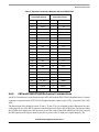
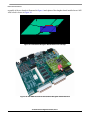
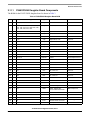
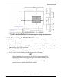
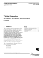
Freescale Semiconductor
Application Note
Document Number: AN2639
Rev. 1, 09/2005
TV-Out Extension
MC9328MX1, MC9328MXL, and MC9328MXS
By: Marcos Nodar
1
Abstract
This document provides information to set-up and use
the Television Output (TV-out) of the FS453/FS454
daughter board with either the MC9328MX1ADS or
MC9328MXLADS (i.MX ADS) Application
Development System and includes references to design
an application with the i.MX processors using the
FS453/FS454 video scan converter processor from
Focus Enhancement, Inc. The FS453/FS454 daughter
board provides an interface between the i.MX LCD
Controller and a TV set. The designs in this application
note are based on the FS453/FS454 processor, that
converts LCD signals to TV signals. Connect the
FS453/FS454 daughter board to the TV by using either a
SCART, an s-video, or composite video interface.
This document applies to the following i.MX devices,
collectively called i.MX throughout:
• MC9328MX1
• MC9328MXL
• MC9328MXS
© Freescale Semiconductor, Inc., 2005. All rights reserved.
Contents
1
2
3
4
5
Abstract . . . . . . . . . . . . . . . . . . . . . . . . . . . . . . . . .1
Architecture and Functional Description . . . . . .2
Electrical Characteristics . . . . . . . . . . . . . . . . . .2
Software Resources . . . . . . . . . . . . . . . . . . . . . .20
References . . . . . . . . . . . . . . . . . . . . . . . . . . . . .20
Architecture and Functional Description
NOTE
The LCD/touch panel module provided in the i.MX ADS kit cannot be used
at the same time as the FS453/FS454 daughter board.
2
Architecture and Functional Description
The environment for the reference design is i.MX ADS, together with a daughter board developed around
Focus Enhancements FS453/FS454 processor. Figure 1 shows a high-level block diagram of the daughter
board configuration.
i.MX1
or
i.MXL
ADS
FS453
Daughter
Board
LCDC Connector, I2C, and Clock
Video Connector, RCA, or SCART
Figure 1. TV Output on i.MX ADS Concept Diagram
The design of the daughter board is based on the FS453/FS454 video scan converter processor. For more
information of the processor’s functionality, please refer to FS453/FS454 PC to TV Video Scan Converter
Product Brief and the FS453/FS454 Hardware Reference Manual, that can be obtained by contacting
Focus Enhancements, Inc. (http://www.focusinfo.com)
The i.MX ADS sends an image from the display buffer of its LCDC interface which is connected to the
digital data input of FS453/FS454 daughter board. The received image is converted into an analog format
that can be displayed on a TV monitor.
3
Electrical Characteristics
This section describes the power requirements of the FS453/FS454 daughter board. The FS453/FS454
processor uses two different supply voltages:
•
•
3.1
+3V for I/O supply voltage
+1.8V for the core voltage
I/O Supply
Typically the power for the I/O supply is provided by the i.MX ADS board. The FS453/FS454 daughter
board also allows connection of a +3V supply from an external power source for debug purposes. A jumper
or a zero ohm resistor is used to select the power source used by the FS453/FS454 daughter board.
TV-Out Extension Application Note, Rev. 1
2
Freescale Semiconductor
Electrical Characteristics
3.2
Core Supply
A regulator on the daughter board generates +1.8 V for the FS453/FS454 processor from the +3V I/O
power input. The part number of the regulator used is MC78PC18NTR from ON Semiconductor, and it
provides currents up to 150 mA. The core supply has a typical current draw of 75 mA.
A zero ohm resistor on the +3.3V and the +1.8V power supply traces of the i.MX ADS is provided to allow
the measurement of the daughter board power consumption.
3.3
Disabling the FS453/FS454 Daughter Board Output
When TV output is not required from the FS453/FS454 daughter board do not to disable it by removing
the power, because it is possible that the i.MX ADS LCD Controller will continue to send signals on its
bus. The FS453/FS454 processor can be damaged without power.
The correct way to disable the output of the FS453/FS454 board is to place the daughter board in
low-power mode by disabling its 27 MHz clock input. This causes the processor to become inactive, and
its inputs are no longer sensitive to LCDC signals from the i.MX ADS. The 27 MHz clock on the
FS453/FS454 daughter board is controlled by a GPIO signal from the i.MX ADS. Turning off the 27 MHz
clock does not affect i.MX operation on the i.MX ADS, unless the FS453/FS454 processor is configured,
as suggested later in this application note, to provide the 16 MHz clock to the i.MX ADS. In this
configuration, continuing normal operation of the i.MX ADS with the FS453/FS454 daughter board
disabled, requires using the 32 kHz reference clock of the i.MX ADS to generate the 16 MHz signal
thereby allowing the i.MX ADS to continue normal operation when the FS453/FS454 daughter board is
disabled.
3.4
Clock Distribution and Control
This section describes several ways to control the clock of the i.MX ADS and the FS453/FS454 daughter
board. It also describes the location of the points where the user can change the divider settings for the
TV-out system. Also refer to the i.MX and FS453/FS454 processor’s PLL settings in their respective
reference manuals.
3.4.1
i.MX PLL Clock Distribution
Figure 2 shows the PLL Clock module of the i.MX processor. The LCD Controller uses the PERCLK2
clock output from the PLL Clock module.
TV-Out Extension Application Note, Rev. 1
Freescale Semiconductor
3
Electrical Characteristics
OSC32
OSC_EN
OSC16
0
CLK16M
CLK32
SYNC Logic
RTC
HCLK
1
System System PLLCLK
PLL
1
USBDIV
CLK48M
USB
0
CLK16_SEL
System_SEL
FCLK
PRESC
BCLKDIV
PREMULT
HCLK
System
PERCLK1
PCLKDIV1
PERCLK2
PCLKDIV2
OSC32
XTALOSC
CPU
BCLK
MCU PLL
CLK32
Internal
Peripherals
PERCLK3
PCLKDIV3
000
SPLLEN
PLL Stop &
Wake-Up Logic
MPLLEN
HCLK
CLK48M
CLK16M
PREMCLK
FCLK
CLKO
CLKO
CLK0SEL [2:0]
Figure 2. i.MX PLL Clock Controller
3.4.2
LCDC and FS453/FS454 Timing
This section describes the operation of the LCDC as it relates to the generation of clock signals required
by the FS453/FS454 daughter board. For programming details for the clock settings refer to the i.MX
processor’s data sheet (see Section 5, “References” on page 20).
The FS453/FS454 processor requires two separate clock signals to operate: a 27 MHz reference clock and
a pixel clock used to control data transfers from the i.MX processor to the FS453/FS454 processor. The
frequency of the pixel clock signal can range from 13.5 MHz to 150 MHz. The i.MX ADS cannot produce
a 27 MHz signal that can be used as a reference clock by the FS453/FS454 processor so it is necessary to
produce the reference clock signal using external components. See Section 3.5, “FS453/FS454 Clocking
and Modes of Operation” on page 6 for more details on how this is done.
The LCDC clock (LSCLK) signal from the i.MX ADS can be programmed to produce an output of
16 MHz which can be used as the pixel clock signal for the FS453/FS454 processor. The LSCLK is an
internally generated output signal that is not available as an external reference signal. See Figure 3.
The frequency of the LSCLK is controlled by the following settings:
• System PLL setting—A combination of prescalers and dividers (SPCTL0 register) are used to set
the System PLL to any value up to the maximum recommended frequency of System PLL, which
is 96 MHz.
TV-Out Extension Application Note, Rev. 1
4
Freescale Semiconductor
Electrical Characteristics
•
•
PERCLKDIV setting—Clock dividers between the PLL and the LCDC module (PCDR register)
modify PERCKLK2 output, which can vary from “divide by 2” to “divide by 16”.
PCD—Pixel Clock Divider in Panel Configuration in the Panel Configuration Register (PCR)
permits dividing the signal clock coming from PLL module, the divider values range from 2 to 64.
The LSCLK value must be less than or equal to 1/5 HCLK (System clock) and the maximum
recommended frequency of System PLL, which is 96 MHz. means that LSCLK has a maximum frequency
of 16 MHz. Because the pixel clock input to the FS453/FS454 processor (the clock that controls data
transfers from i.MX ADS) can range from 13.5 MHz to 150 MHz a LSCLK signal of 16 MHz allows for
a maximum possible throughput between the LCDC and the FS453/FS454 processor.
data input
clock
FIFO
Shift register
Memory + ARM920T
DMA Data input
HCLK
SysPLL
BCLKdiv
LD[0..15]
PCD
Divide by N+1
Divide by 1..16
PixCLK
SysPLL
Perclkdiv2
Divide by 1..16
LCDC_CLK
Div by 8,4,2,1
LSCLK
Figure 3. LCDC Clock and Data Signals
Figure 4 summarizes the registers in the i.MX processor that control the output frequency of the i.MX
ADS.
Possible Ref Clock
Sources
PLL Module
LCDC Module
16 MHz
16 MHz xtal
16.384 MHz
32 kHz xtal x 512
System PLL
SPCTL0 Register
PERCLKDIV2 Field
in PCRD Register
PCD Field in
PCR Register
LSCLK
Figure 4. LSCLK Clock Settings in i.MX ADS
TV-Out Extension Application Note, Rev. 1
Freescale Semiconductor
5
Electrical Characteristics
3.5
FS453/FS454 Clocking and Modes of Operation
The FS453/FS454 processor has several modes of operation, depending on the clock distribution (see
FS453/FS454 Hardware Reference Manual, section 9.4.3, from Focus Enhancements for further details).
This application note describes two possible configurations to connect the clocks.
3.5.1
Using an External PLL
One mode which is compatible with the i.MX processor is slave mode because the i.MX LCD Controller clock
is derived from the internal system clock. The oscillator references for i.MX are 32 kHz or 16 MHz. The
reference for FS453/FS454 must be 27 MHz. The CLKO pin on the i.MX is programmable and would seem as a good source
to derive the 27 MHz needed by the FS453/FS454. However, a 27 MHz value cannot be achieved with a System PLL running
at 96 MHz because the USB requires a signal frequency of 48 MHz and it is derived directly from the system PLL. Therefore,
an external 27 MHz oscillator is required to provide the reference clock signal to the FS453/FS454 daughter board.
3.5.2
Using a 27 MHz Crystal
Another alternative is to share the same external 27 MHz reference oscillator between i.MX ADS and the
FS453/FS454 processor as shown in Figure 5. By programing the FS453/FS454 processor to output a
16 MHz clock from the 27MHz crystal, the 16 MHz signal can then be used as a reference for the
MC9328MX1 (the MC9328MXL does not use a 16 MHz reference). In this configuration, the
FS453/FS454 processor is used in slave mode. This solution avoids the need for an external 16 MHz
oscillator while the 32 kHz crystal is necessary to DBMX-1 in either configuration.
NOTE
The 27 MHz crystal used must have a frequency tolerance of less than a
50 ppm in parallel resonance (not series).
16MHz
PLL
Use 16MHz
reference
FS453
I/Os
LCDC
PLL
LD[15..0]
32kHz
i.MX
DBMX
19.2MHz
19.2MHz
27MHz
Figure 5. Using a Shared 27 MHz Crystal to Create Reference Frequencies
TV-Out Extension Application Note, Rev. 1
6
Freescale Semiconductor
Electrical Characteristics
3.6
FS453/FS454 Connections
The physical connectors on the FS453/FS454 daughter board are as follows:
• Power connector—Allows connection of an external +3V to the board in case the i.MX ADS
cannot provide sufficient current. If this connector is used the resistor R17 must be removed to
isolate the power supplies of the i.MX ADS and the daughter board. The power connector is a
2.54 mm HE34 connector
• LCDC interface—Mini-DIN 7 pin
• Video Output Interface—RCA connector
3.7
i.MX ADS Connections
Figure 6 shows the LCDC signal connections that are available on the i.MX ADS. The MC9328MX1 LCD
Controller was designed to interface with a Sharp LCD panel and therefore some signals are unique to it.
Descriptions of the LCDC signals are provided in Table 1.
Figure 6. LCDC Connector on i.MX ADS
Table 1. LCDC Signal Description
Name
LD [15:0]
Description
LCD Data Bus – All LCD signals are driven low after reset and when LCD is off.
FLM/VSYNC Frame Sync or Vsync, it also serves as the clock signal output for gate
driver (dedicated signal SPS for Sharp panel HR-TFT).
LP/HSYNC
Line pulse or H sync
LSCLK
Shift clock
ACD/OE
Alternate Crystal Direction / Output Enable
CONTRAST This signal is used to control the LCD bias voltage as contrast control.
SPL_SPR
Program horizontal scan direction (Sharp panel dedicated signal).
TV-Out Extension Application Note, Rev. 1
Freescale Semiconductor
7
Electrical Characteristics
Table 1. LCDC Signal Description (continued)
Name
Description
PS
Control Signal output for source driver (Sharp panel dedicated signal).
CLS
Start signal output for gate driver. This signal is invert version of PS (Sharp panel dedicated signal).
REV
Signal for common electrode driving signal preparation (Sharp panel dedicated signal).
Note: Signals that appear on the LCDC connector that are not listed in this table are for touchscreen control and do not apply to
this application note.
The signals on the i.MX ADS that are used to connect the FS453/FS454 daughter board are:
• LSCLK
• LD[0.15]
• VSYNC
• HSYNC
VCC and GND are for the i.MX ADS power supply. MX works under 3V and supports I/O voltage of VCC
+0.2V. According to FS453/FS454 processor’s hardware reference manual, it can operate using voltages
between +3V and +3.6V, which makes it compatible with DBMX NVDD voltage supply.
3.8
i.MX ADS FS453/FS454 Quick Start Summary
This section provides a summary of how to quickly interface the FS453/FS454 daughter board with the
i.MX ADS. Detailed instructions about the modifications, software resources, PCB layout, and schematics
are found later in this application note.
NOTE
The 16 MHz crystal on the i.MX ADS does not need to be unsoldered, but
a header is needed to connect to the FS453/FS454 daughter board.
3.8.1
Modifications on i.MX ADS
These modifications permits the daughter board to be plugged into i.MX ADS:
1. Remove the 16 MHz oscillator, Y7, and solder a pin on EXT_16M test point.
2. Connect wires from I2C port to the LCDC connector. Pins A8 (I2C_CLOCK) and C8 (I2C_DATA)
of the P20 connector (CSI connector) must be connected to pins 23 (I2C_CLOCK) and 21
(I2C_DATA) of the LCDC connector (P8).
TV-Out Extension Application Note, Rev. 1
8
Freescale Semiconductor
Electrical Characteristics
3.8.2
Software Installation
The following instructions provide instruction to install the software needed to launch and run the
FS453/FS454 processor from the i.MX ADS. The application that permits initialization of the system is
/launch.consoleApp. For help with all functions of the application type '?'.
1. Install the components provided (boot loader, kernel, and root disc). The boot loader is the same as
standard BSP releases, whereas the kernel was specially rebuilt to support VGA frame buffer. The
root disc contains the drivers for the FS453/FS454 processor.
3.8.3
Modifications Required on the i.MX ADS
The interface for the FS453/FS454 daughter board requires three modifications on the i.MX ADS, two
modifications for the I2C on the LCD connector and one modification for the 16 MHz clock on the
16 MHz crystal.
3.8.3.1
LCD Connector and Layout Modifications
It is recommended to limit the number of connectors between the i.MX ADS and the daughter board. The
LCD connector has enough pins to route all the signals in and out from the i.MX ADS, because the
standard LCD interface uses only 20 of the 34 available pins. To achieve the functional interface, some
signals are brought out from the LCD connector to replace the dedicated signals for the Sharp LCDs
interface.
The FS453/FS454 daughter board interface requires four more I/Os signals than exist on the i.MX ADS
LCD connector.
• I2C—It is recommended for I2C signals to share the same connector as the LCDC to limit the
number of connections between i.MX ADS and FS453/FS454 daughter board.
• Two wires must be drawn from A8 and C8 pins of CSI connector of the i.MX ADS to route the
signals to pins 21 and 23 of the LCD connector.
— I2C data (C8 on CSI connector) is pin 21 of LCD connector.
— I2C clock (A8 on CSI connector) is pin 23 of LCD connector.
• Power—Controlled using a GPIO from the i.MX processor. This pin controls the FET on the
FS453/FS454 daughter board, which gates the 27 MHz clock to the FS453/FS454 processor, to
reduce power consumption when TV-out is not used. No rework is necessary for this pin, because
it is internally multiplexed with GPIO Port D7 in the i.MX processor. The pin for this I/O is pin 22
but this pin must not be used if a crystal is used to clock the FS453/FS454 processor.
• Reset—Connected using a GPIO from the i.MX processor. This pin is directly connected to a pin
of the FS453/FS454 to control its reset. The pin for this I/O is pin 24.
These four signals are located on unused pins of the LCD connector (instead of the signals required for
Sharp LCD). This supposes that the sharp LCD will not be used on the modified i.MX ADS. All four of
these pins are used as general purpose inputs at reset, therefore ensuring that the modifications will not
cause shorts at reset.
The new mapping of the connector is shown in Figure 7. Pins that are modified are shown with asterisks.
TV-Out Extension Application Note, Rev. 1
Freescale Semiconductor
9
Electrical Characteristics
LP
1
2
LSCLK
LACD
3
4
FLM
LP
4
6
LD3
LD4
7
8
LD1
LD2
9
10
LD9
LD10
11
12
LD1
LD8
13
14
LD9
LD15
15
16
LD7
LD13
17
18
LD14
CONTRAST
19
20
MISO
I2C_DAT*
21
22
PWR_GPIO*
I2C_CLK*
23
24
TV_RST*
LD0
25
26
GND
LD6
27
28
LD5
LD11
29
30
GND
TOP
31
32
BOTTOM
LEFT
33
34
RIGHT
Note: Asterisks indicate modified pins.
Figure 7. Modified i.MX ADS Connector
LCDC
LCDC
I2C
I2C
PLL
CLK
OUTPUT
FS453
Reset
2 GPIOs
FET
MX1/MXL ADS
FS453 daughterboard
Exists on LCD connector of ADS
To be brought on LCD connector of ADS
Dedicated header
Figure 8. Signal Availability on LCD Connector of i.MX ADS
3.8.4
i.MX and FS453/FS454 Electrical Connections
The electrical connections between the i.MX ADS and the FS453/FS454 daughter board are summarized
in Table 2.
TV-Out Extension Application Note, Rev. 1
10
Freescale Semiconductor
Electrical Characteristics
Table 2. Electrical Connections Between i.MX and FS453/FS454
i.MX
256-pin BGA package
3.8.5
FS453/FS454
80-pin QFP package
Pin
Pin Name
Pin
Pin Name
J14
LD11
8
P3
K12
LD12
9
P4
K13
LD13
10
P5
K14
LD14
11
P6
K16
LD15
12
P7
H14
LD5
15
P10
J11
LD6
16
P11
J12
LD7
17
P12
J13
LD8
18
P13
H15
LD9
23
P14
K11
LD10
24
P15
H11
LD0
28
P19
G16
LD1
29
P20
H12
LD2
32
P21
H16
LD3
33
P22
H13
LD4
34
P23
G14
LP/HSYNC
35
HSYNC
G15
FLM/VSYNC
36
VSYNC
G13
ACD/OE
38
BLANK
P14
I2C_SCL
45
SCLK
P15
I2C_SDA
44
SDATA
N/A
GPIO
53
RESETL
F15
LSCLK
54
CLKIN_P
T15
EXTAL16M
56
CLKOUT
i.MX and FS453/FS454 Mechanical Considerations
An HE10-34 connector is used to interface the i.MX ADS with the FS453/FS454 daughter board. A female
connector is required on the FS453/FS454 daughter board to connect to the LCDC connector of the i.MX
ADS.
The dimensions of the board layout are 50 mm × 70 mm. The size is limited to these dimensions because
of the physical size of the HE34 connector and the dimensions of the i.MX ADS layout. The pin providing
the 16 MHz clock input to the i.MX processor is near the center of the i.MX ADS board. The wire carrying
this HF signal must be kept as short as possible to preserve the 16 MHz clock signal integrity. The
TV-Out Extension Application Note, Rev. 1
Freescale Semiconductor
11
Electrical Characteristics
assembly of the two boards is illustrated in Figure 9 and a photo of the daughter board installed on an i.MX
ADS board is shown in Figure 10.
i.MX ADS
i.MX JTAG
Connector
Spacer
FS453
Daughterboard
50mm
16MHz
clock header
FS453 chip
70mm
Video Connector
HE34 Connector
Figure 9. FS453/FS454 Daughter Board Mechanical Concept
Figure 10. i.MX ADS Board with FS453/FS454 Daughter Board Mounted
TV-Out Extension Application Note, Rev. 1
12
Freescale Semiconductor
Electrical Characteristics
NOTE
When designing a new board, special care must be taken regarding the
placement of the JTAG connector—which will be very close to the daughter
board. It must not interfere with the JTAG connector.
3.9 FS453/FS454 PCB Modification Guidelines
The FS453/FS454 daughter board consists of four layers. The physical locations of the components are
shown in Figure 11 on page 14 and a photograph of the PCB is shown in Figure 12 on page 14.
The layer stratus is defined as follows:
• Layers 0 and 3 for signals
• Layers 1 and 2 for power and ground planes
While this design allows for modifications and easy probing, the design is not optimal in terms of EMI and
shielding. The following design practices are recommended:
• Place components associated with the FS453/FS454 daughter board as close as possible to their
respective pins.
• Locate the FS453/FS454 daughter board near the power supply connector, the video input
connector, and the video output connector.
• Place the FS453/FS454 daughter board above a solid ground plane to shield EMI radiation.
• Do not route signal traces under the FS453/FS454 daughter board.
3.9.1
EMC Constraints
Consult the FS453/FS454 Physical Reference Manual for further details on the layout and routing
constraints and guidelines associated with the FS453/FS454 processor.
The following guidelines are recommended for the interconnection of the i.MX ADS and the
FS453/FS454 daughter board:
• The tracks carrying signals from the LCDC must be the same length to ensure good coherence with
the clock.
• I2C clock and data must be close to each other and the same length.
• Special care should be used in the length and placement of the wire carrying the CLKOUT
(16 MHz output).
• The length of all outputs to the TV must be the same.
3.9.2
Test Points
The following test points are available:
• CLKIN_P, CLKIN_N
• CLKOUT
• LSCLK
TV-Out Extension Application Note, Rev. 1
Freescale Semiconductor
13
Electrical Characteristics
•
•
GND (place several headers for easy probing)
I2C_DAT and I2C_CLK
34
Power Supply
Section
FS454
HE10-34
Clocks Section
16 MHz
Clock Header
33
RCA
DIN
Video Connectors
2
1
Figure 11. Layout Diagram of FS453/FS454 Daughter Board
Figure 12. Photo of Daughter Board
3.10
FS453/FS454 Daughter Board Reference Design
This section provides the detailed information about the design of a TV-out daughter board based on
FS453/FS454 processor for the i.MX ADS.
3.10.1
Reference Schematic
The schematic for the FS453/FS454 daughter board is shown in Figure 13.
TV-Out Extension Application Note, Rev. 1
14
Freescale Semiconductor
Electrical Characteristics
Figure 13. FS453/FS454 Daughter Board Schematic
TV-Out Extension Application Note, Rev. 1
Freescale Semiconductor
15
Electrical Characteristics
3.11
FS453/FS454 PCB Layout
The top and bottom views of the FS453/FS454 daughter board are shown in Figure 14 and Figure 15.
Figure 14. Top View of the FS453/FS454 Daughter Board
Figure 15. Bottom View of the FS453/FS454 Daughter Board
TV-Out Extension Application Note, Rev. 1
16
Freescale Semiconductor
Electrical Characteristics
3.11.1
FS453/FS454 Daughter Board Components
The BOM for the FS453/FS454 daughter board is shown in Table 3.
Table 3. FS453/FS454 Daughter Board BOM
Item
Qty
Reference Designator
Type
1
4
C1,C13,C16,C23
Cap.
22uF, 16v, Al
Panasonic
2
20
C2, C3, C4, C5, C6, C14, C17, C18,
C21, C22, C24, C27, C28, C29, C30,
C31, C32, C35, C37, C38
Cap.
0.1uF, 16V, X7R
ROHM
3
3
C7,C9,C11
Cap.
47pF, 50V, NPO
PHILIPS
4
3
C8,C10,C12
Cap.
68pF, 50V, NPO
PHILIPS
5
2
C25,C15
Cap.
0.01uF, 50V, Y5V
Panasonic
6
1
C19
Cap.
270pF, 50vdc, X7R
Panasonic
7
1
C20
Cap.
330pF, 16vdc, X7R
Panasonic
8
2
C36,C26
Cap.
10uF, 10v, Tant.
KEMET
9
2
C34,C33
Cap.
27pF, 50V, COG
Panasonic
10
4
D1,D2,D3,D4
Diode
Dual hi-speed diode
ZETEX
11
3
FB1,FB2,FB3
Ferrite Bead
FB 70@100MHz
Allied Components Intl.
12
1
J2
S-video/RGB/HDTV
KYCON
13
3
L1,L2,L3
Inductor
0.33uH
Allied Components Intl.
14
1
L4
Inductor
1.8uH
Allied Components Intl.
15
4
R1,R2,R3,R4
Res.
75.0, 1/16w, 1%
Panasonic
16
1
R5, R16
Res.
33, 2/16w, 5%
Panasonic
17
1
R6
Res.
4.7, 1/16w, 5%
Panasonic
18
1
R7
Res.
100, 1/16w, 5%
Panasonic
19
1
R8
Res.
549, 1/16w,1%
Panasonic
20
1
R9
Res.
475, 1/16w,1%
Panasonic
21
2
R11,R10
Res.
4.7K, 1/16w, 5%
Panasonic
22
1
R12
Res.
1M, 1/16w, 5%
Panasonic
23
1
U1
I.C.
FS453/FS454
FCSE
24
1
U2
I.C.
78PC18 VReg
ON Semiconductor
25
1
Y1
XTAL
27MHz, 30ppm,18pf,
BT-cut, fundamental mode
MMD Components
26
1
R18
Res.
0 Ohm
–
27
1
R17
Res.
0 Ohm
–
28
1
Y2
OSC
27MHz
29
1
J1
Conn.
HE10-34 female connector
–
30
1
P2
Conn.
Bornier pas de 3.81
–
Conn.
Part
Manufacturer
AVX
TV-Out Extension Application Note, Rev. 1
Freescale Semiconductor
17
Electrical Characteristics
Table 3. FS453/FS454 Daughter Board BOM (continued)
Item
Qty
31
1
P5
Conn.
Female header
–
32
1
P4
Conn.
Male header
–
33
1
J3
Conn.
RCA connector
–
3.12
Reference Designator
Type
Part
Manufacturer
i.MX Processor Software Configurations
Information regarding the register settings, programming the FS453/FS454 processor, and software
resources are provided in this section.
3.12.1
Register Settings
To have good display quality on the TV connected to the TV-out signal, the minimum recommended
picture size is 640 × 480. To achieve this output format from the LCDC, the register configuration must
be as follows:
• Virtual Page Width register (VPW) that reflects the dimensions of the image in memory.
• SIZE registers to indicate in XMAX and YMAX the size of the image to be displayed.
Figure 16 shows the respective definitions of SIZE and VPW. SSA refers to the start address of the display
buffer.
Other registers that affect the display of the image are Horizontal Configuration Register and Vertical
Configuration Register (HCR and VCR). The meaning of the values present in these registers (H_WIDTH,
H_WAIT2, H_WAIT1 and V_WAIT1, V_WIDTH, V_WAIT2 are represented in Figure 16.
Virtual Page Width (VPW)
Screen Starting Address (SSA)
Screen Height (YMAX)
Virtual Page Height (VPH)
Screen Width (XMAX)
Figure 16. LCD Screen Format
TV-Out Extension Application Note, Rev. 1
18
Freescale Semiconductor
Electrical Characteristics
Figure 17. Horizontal and Vertical Configuration Register Timings and Relationships
3.12.2
Programming the FS453/FS454 Processor
The FS453/FS454 processor’s internal registers are programmed by the i.MX through the I2C interface.
An overview of the procedure follows:
1. Program the FS453/FS454 processor to generate a 16 MHz clock from the 27 MHz crystal.
2. Switch the internal clock source of the i.MX processor from its local 32 kHz crystal to the 16 MHz
input from the FS453/FS454 processor.
3. Program the FS453/FS454 processor to apply scaling to the i.MX image data from VGA to fit the
selected TV output format (PAL, NTSC).
4. The TV screen will now display data correctly from the LCD output.
NOTE
When switching to low-power mode, the i.MX processor must switch its
internal clock source back to its local 32 kHz crystal before turning off the
FS453/FS454 processor’s 27 MHz crystal.
eLinux routines to support this application developed for the i.MX
processor tools are posted on Freescale's website.
TV-Out Extension Application Note, Rev. 1
Freescale Semiconductor
19
Software Resources
4
Software Resources
The sources for the application software rely on the following files.
•
•
•
•
•
5
SIO_MX1.c file: sets up i.MX processor’s I2C module and provides functions to read and write
FS453/FS454 processor's registers.
DM_elinux_BSP.c: provides functions for direct memory reads and writes of Words, Halfwords
and Bytes in i.MX.
OS_elinux_BSP.c: contains 2 wait functions.
Textui.c: contains the functions for the text console interface
ConsoleApp.c: main program to launch the application.
References
Documents from Focus Enhancements Inc.:
• FS453/FS454 Product Brief
• FS453/FS454 Hardware Reference
• FS453/FS454 Software Reference
• FS453/FS454 Daughter Board
• FS453/FS454 Physical Reference
• i.MX and FS453/FS454 PLL Settings
Documents from Freescale:
• MC9328MX1 Integrated Portable System Processor Reference Manual
(order number: MC9328MX1RM/D)
• MC9328MX1 Integrated Portable System Processor Data Sheet (order number: MC9328MX1/D)
• MC9328MXL Integrated Portable System Processor Reference Manual
(order number: MC9328MXLRM/D)
• MC9328MXL Integrated Portable System Processor Data Sheet (order number: MC9328MXL/D)
• M9328MX1ADS Schematics (order number: M9328MX1ADS_V2_0)
• M9328MX1ADS Application Development System User's Manual
(order number: M9328MX1ADS_A_UM)
TV-Out Extension Application Note, Rev. 1
20
Freescale Semiconductor
NOTES
TV-Out Extension Application Note, Rev. 1
Freescale Semiconductor
21
How to Reach Us:
Home Page:
www.freescale.com
E-mail:
[email protected]
USA/Europe or Locations Not Listed:
Freescale Semiconductor
Technical Information Center, CH370
1300 N. Alma School Road
Chandler, Arizona 85224
+1-800-521-6274 or +1-480-768-2130
[email protected]
Europe, Middle East, and Africa:
Freescale Halbleiter Deutschland GmbH
Technical Information Center
Schatzbogen 7
81829 Muenchen, Germany
+44 1296 380 456 (English)
+46 8 52200080 (English)
+49 89 92103 559 (German)
+33 1 69 35 48 48 (French)
[email protected]
Japan:
Freescale Semiconductor Japan Ltd.
Headquarters
ARCO Tower 15F
1-8-1, Shimo-Meguro, Meguro-ku,
Tokyo 153-0064, Japan
0120 191014 or +81 3 5437 9125
[email protected]
Asia/Pacific:
Freescale Semiconductor Hong Kong Ltd.
Technical Information Center
2 Dai King Street
Tai Po Industrial Estate
Tai Po, N.T., Hong Kong
+800 2666 8080
[email protected]
For Literature Requests Only:
Freescale Semiconductor Literature Distribution Center
P.O. Box 5405
Denver, Colorado 80217
1-800-521-6274 or 303-675-2140
Fax: 303-675-2150
[email protected]
Document Number: AN2639
Rev. 1
09/2005
Information in this document is provided solely to enable system and software implementers to use
Freescale Semiconductor products. There are no express or implied copyright licenses granted
hereunder to design or fabricate any integrated circuits or integrated circuits based on the information
in this document.
Freescale Semiconductor reserves the right to make changes without further notice to any products
herein. Freescale Semiconductor makes no warranty, representation or guarantee regarding the
suitability of its products for any particular purpose, nor does Freescale Semiconductor assume any
liability arising out of the application or use of any product or circuit, and specifically disclaims any
and all liability, including without limitation consequential or incidental damages. “Typical” parameters
that may be provided in Freescale Semiconductor data sheets and/or specifications can and do vary
in different applications and actual performance may vary over time. All operating parameters,
including “Typicals”, must be validated for each customer application by customer’s technical experts.
Freescale Semiconductor does not convey any license under its patent rights nor the rights of others.
Freescale Semiconductor products are not designed, intended, or authorized for use as components
in systems intended for surgical implant into the body, or other applications intended to support or
sustain life, or for any other application in which the failure of the Freescale Semiconductor product
could create a situation where personal injury or death may occur. Should Buyer purchase or use
Freescale Semiconductor products for any such unintended or unauthorized application, Buyer shall
indemnify and hold Freescale Semiconductor and its officers, employees, subsidiaries, affiliates, and
distributors harmless against all claims, costs, damages, and expenses, and reasonable attorney
fees arising out of, directly or indirectly, any claim of personal injury or death associated with such
unintended or unauthorized use, even if such claim alleges that Freescale Semiconductor was
negligent regarding the design or manufacture of the part.
Freescale™ and the Freescale logo are trademarks of Freescale Semiconductor, Inc. The ARM
Powered Logo is a registered trademarks of ARM Limited. All other product or service names are the
property of their respective owners.
© Freescale Semiconductor, Inc. 2005. All rights reserved.