1
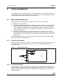
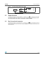
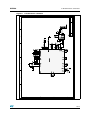
AN2168
Application note
ST10F27x hardware development
Getting started
Introduction
The ST10F27x MCUs are derivatives of the STMicroelectronics ST10 family of 16-bit CMOS
microcontrollers. They combine high CPU performance (CPU frequency up to 64 MHz) with high
peripheral functionalities and enhanced I/O-capabilities. They offer on-chip high speed single voltage
Flash memory, on-chip high speed RAM and support clock generation via PLL or an external clock. The
ST10F27x MCUs also provide an enhanced 16-bit DSP co-processor to improve their performance in
signal processing algorithms.
This application note complements the ST10F27x datasheet and user manual by describing the minimum
hardware environment required to build an application around the ST10F27x. A number of features of the
ST10F27x devices are described in the first five chapters. In the sixth, a basic schematic is given
illustrating the minimum hardware required to get the ST10F27x running. For a deeper description of
these features, refer to the ST10F27x datasheet or user manual.
In order to build an application around ST10F27x, the application board should, at least, provide the
following features:
■
Power supply
■
Clock management
■
Reset control
■
Boot mode settings
September 2013
Rev 3
1/15
www.st.com
15
AN2168
Contents
1
2
Power supply . . . . . . . . . . . . . . . . . . . . . . . . . . . . . . . . . . . . . . . . . . . . . . . . . 3
1.1
Overview . . . . . . . . . . . . . . . . . . . . . . . . . . . . . . . . . . . . . . . . . . . . . . . . . . . . . 3
1.2
Pin Vstby / EA . . . . . . . . . . . . . . . . . . . . . . . . . . . . . . . . . . . . . . . . . . . . . . . . . 3
Clock management . . . . . . . . . . . . . . . . . . . . . . . . . . . . . . . . . . . . . . . . . . . . 4
2.1
2.2
3
Main clock control unit . . . . . . . . . . . . . . . . . . . . . . . . . . . . . . . . . . . . . . . . . . 4
2.1.1
Direct Drive operation . . . . . . . . . . . . . . . . . . . . . . . . . . . . . . . . . . . . . . . . . . . 4
2.1.2
Prescaler operation . . . . . . . . . . . . . . . . . . . . . . . . . . . . . . . . . . . . . . . . . . . . . 4
2.1.3
PLL operation . . . . . . . . . . . . . . . . . . . . . . . . . . . . . . . . . . . . . . . . . . . . . . . . . 5
32 kHz low power oscillator . . . . . . . . . . . . . . . . . . . . . . . . . . . . . . . . . . . . . . . 5
Reset management . . . . . . . . . . . . . . . . . . . . . . . . . . . . . . . . . . . . . . . . . . . . 7
3.1
External reset circuitry . . . . . . . . . . . . . . . . . . . . . . . . . . . . . . . . . . . . . . . . . . 7
3.2
How to reset external devices with ST10F27x reset signals . . . . . . . . . . . . . . 7
3.2.1
RSTOUT pin . . . . . . . . . . . . . . . . . . . . . . . . . . . . . . . . . . . . . . . . . . . . . . . . . . 8
3.2.2
Bidirectional reset . . . . . . . . . . . . . . . . . . . . . . . . . . . . . . . . . . . . . . . . . . . . . . 8
4
Start up configuration . . . . . . . . . . . . . . . . . . . . . . . . . . . . . . . . . . . . . . . . . . 9
5
Boot management . . . . . . . . . . . . . . . . . . . . . . . . . . . . . . . . . . . . . . . . . . . . 10
5.1
Bootstrap loader . . . . . . . . . . . . . . . . . . . . . . . . . . . . . . . . . . . . . . . . . . . . . . 10
5.2
Single chip mode . . . . . . . . . . . . . . . . . . . . . . . . . . . . . . . . . . . . . . . . . . . . . 11
5.3
Boot from external memories . . . . . . . . . . . . . . . . . . . . . . . . . . . . . . . . . . . . 11
6
ST10F27x basic schematics . . . . . . . . . . . . . . . . . . . . . . . . . . . . . . . . . . . . 12
7
Revision history . . . . . . . . . . . . . . . . . . . . . . . . . . . . . . . . . . . . . . . . . . . . . . 14
2/15
AN2168
1 Power supply
1
Power supply
1.1
Overview
The ST10F27x devices are processed in 0.18 µm technology. ST10F27x core logic and I/O
peripherals need different power supplies. In fact, ST10F27x core logic operates with an 1.8V
power supply while the I/O peripherals operate with a power supply in the 4.5V to 5.5V range.
The ST10F27x devices are single supply. This means that just one external supply of 5V is
necessary to feed both core and peripherals. The power management block includes a
regulator to provide the core logic 1.8V supply from the 5V input supply.
The internally generated 1.8V supply is available on pin V18 (pin 56) of the ST10F27x. No
external supply can be connected to V18. A decoupling ceramic capacitor of a typical value
10nF(max 100nF) has to be connected between the V18 pin and the nearest Vss pin. The main
purposes of this capacitor are to:
●
compensate voltage drops due to pulsive current sinked by the device.
●
close the feedback loop of the internal voltage regulator making the system stable.
A capacitor of a value 100nF has to be connected for each couple VDD and the nearest pin
Vss.
1.2
Pin Vstby / EA
On the ST10F27x, the pin 99 provides two functionalities:
●
VSTBY voltage(4.5 - 5.5V) applied on pin 99 maintains the RAM powered when ST10F27x
main power is OFF. It must be applied before switching OFF the main power supply.
●
EA functionality which configures the ST10F27x to start from external memory if its level is
low during reset.
Table 1 contains the different configurations and the needed hardware for each case (if stand
by mode is used or not).
Table 1.
VSTBY/EA
EA = 1
Stand by mode used
VSTBY = 5V when VDD is
turned off
EA = 0
4 .. 5.5 V
EA
Vss
Stand by mode not used
VSTBY = 0V
Vstby Ex
EA/VSTBY
VDD
EA/VSTBY
Vss
EA/VSTBY
Vss
3/15
AN2168
2 Clock management
2
Clock management
Internal operation of CPU and peripherals are controlled by the same main clock named Fcpu.
It is provided by the on-chip clock generator. The RTC module can be controlled either by the
ST10F27x main clock or by the auxiliary 32 kHz oscillator.
2.1
Main clock control unit
The ST10F27x core and peripherals can operate with a frequency up to 64 MHz.
The ST10F27x main clock can be:
●
generated using the ST10F27x internal oscillator amplifier. In this case, the input signal for
the internal oscillator is generated by an external crystal or resonator with a frequency
between 4MHz and 12 MHz, and is connected between XTAL1 and XTAL2: XTAL1 is the
input and XTAL2 is the output. This configuration is available when using on chip PLL or
the prescaler operation.
●
forced by an external clock when the direct drive option is selected. In this case, the
internal oscillator is disabled and neither the external crystal nor resonator is needed. The
external clock is input on the XTAL1 pin of the ST10F27x and the XTAL2 pin must be left
unconnected.
The clock generation mode is selected during reset according to port 0 lines: P0H.5, P0H.6,
P0H.7. Each mode is described below.
2.1.1
Direct Drive operation
When pins P0H.7 = 0, P0H.6 = 1, P0H.5 = 1 during reset, the CPU clock is directly driven from
the external generator connected to XTAL1 pin. In this case, neither the crystal nor the
resonator is used.
ST10F27x Direct Drive
P0H.5 = 1
VDD
P0H.6 = 1
VDD
P0H.7 = 0
8 KOhms
VSS
External Clock
1 .. 64 MHz
Unconnected
2.1.2
XTAL1
ST10F27x
Figure 1.
XTAL2
Prescaler operation
When pins P0H.7 = 0, P0H.6 = 0, P0H.5 = 1 during reset, the CPU clock is derived from the
internal oscillator amplifier. The input clock signal is generated by a crystal or a resonator with a
frequency between 4MHz and 8 Mhz. The CPU frequency is equal to the input signal on pin
XTAL1 divided by 2
4/15
AN2168
2 Clock management
Figure 2.
Prescaler operation
P0H.5 = 1
VDD
VSS
ST10F27x
P0H.6 = 0
P0H.7 = 0
VSS
crystal
XTAL1
XTAL2
For more details, please refer to the ST10F27x datasheet.
2.1.3
PLL operation
For the remaining combinations of pins P0H.7, P0H.6 and P0H.5, the PLL operation is enabled
and provides the ST10F27x with a main clock. The PLL multiplies the input frequency entered
on pin XTAL1 by a factor selected by the pins P0H.7, P0H.6 and P0H.5 levels.
For more details regarding the maximum crystal frequency and the resulted CPU frequency,
refer to ST10F27x datasheet.
Example:
If a 5 Mhz external crystal is used and P0H[7..5] = 101 configuration is selected, ST10F27x will
run with a 40 Mhz frequency. This example is illustrated in the following figure.
Figure 3.
PLL operation example
P0H.5 = 1
VDD
P0H.6 = 0
1MHoms
5 Mhz
crystal
XTAL1
VDD
ST10F27x
P0H.7 = 1
VSS
XTAL2
2.2
32 kHz low power oscillator
When power down mode is entered, the main oscillator generating the ST10F27x main clock is
switched OFF. If the RTC module needs to continue running during power down mode, a
reference clock is needed. Therefore, a 32 kHz crystal is connected to the low power oscillator
pins XTAL3 and XTAL4, in order to give a reference clock to the RTC module if the main
oscillator is stopped.
5/15
AN2168
2 Clock management
32 kHz oscillator
32 Khz
crystal
XTAL3
ST10F27x
Figure 4.
XTAL4
For more details concerning capacitance, refer to ST10F27x Datasheet
If the 32 kHz oscillator is not used, XTAL3 must be tied to ground and XTAL4 must be left
unconnected.
6/15
AN2168
3 Reset management
3
Reset management
3.1
External reset circuitry
Figure 5 and Figure 6 summarize the hardware required to operate a good reset. The first one
should be used when the power down mode is not required by the application, whereas the
second one shows the hardware configuration in order to use the power down mode.
Figure 5.
External reset circuitry when power down mode is not used
VDD
Internal pull-up
of 50 - 250 kOhms
VDD
internal weak pull
down of 200 uA
R0
220K-1M
RPD
RSTIN
Reset Signal
Open Drain Output
External Reset
Circuitry
GND
ST10F27x
Figure 6.
External reset circuitry when power down mode is used
VDD
Internal pull-up
of 50 - 250 kOhms
VDD
internal weak pull
down of 200 uA
R0
220K-1M
RPD
1uF
RSTIN
Reset Signal
Open Drain Output
External Reset
Circuitry
GND
GND
3.2
ST10F27x
How to reset external devices with ST10F27x reset signals
If the application uses the ST10F27x with external devices, such as other microcontrollers, and
if the external devices should be reset by the ST10F27x beyond the ST10 reset, there are two
ways to do this:
●
Using the RSTOUT pin
●
Using the bidirectional reset option provided by the ST10F27x
7/15
AN2168
3 Reset management
3.2.1
RSTOUT pin
RSTOUT signal is used to reset external devices that don’t need initialization before EINIT
instruction of the ST10F27x. In this case, the user can execute some code before initializing the
external device.
EINIT
RSTIN used to reset ST10F27x
RSTOUT used to reset external devices
The reset circuitry on RSTIN and RPD pins used in this case is the same circuitry described in
the previous section.
3.2.2
Bidirectional reset
The bidirectional reset changes RSTIN pin from a pure input to an open drain output with an
integrated pull-up resistor. This mode is used:
●
to convert software and watchdog resets into hardware resets
●
to provide a reset signal to external devices that can’t be connected to RSTOUT pin
because it’s maintained active during the ST10 initialization.
Pin RSTIN may be connected to external reset devices with an open drain output driver to avoid
conflict.
For more details, refer to the ST10F27x datasheet in the section for “bidirectional reset”.
8/15
AN2168
4
4 Start up configuration
Start up configuration
Port 0 is used to select the start up system configuration by the mean of external pull down
resistors. During reset, Port 0 lines are set to input mode with internal pull up resistors. The port
0 pins are read at the end of the reset sequence.
The following table summarizes the port0 lines corresponding to the start up features:
Table 2.
Port 0 fields
Port 0 lines
Function
Comments
P0L.0
Emulation mode
1)
P0L.1
Adapt mode
1)
P0L.4, P0L.5
Boot strap mode
See Section 5: Boot
management
P0L.6, P0L.7
BUSTYP: CS0 Bus type configuration
1)
P0H.0
WRC Write/ Read configuration
1)
P0H.1, P0H.2
CSSEL: Chip Select
1)
P0H.3, P0H.4
SALSEL: CS0 Address Lines
1)
P0H.5.. P0H.7
CLKCFG: Clock configuration
1)
1)
See Section 2: Clock
management
Note: 1 A low level is applied using a pull down resistor of 8 kOhms.
For more details regarding the P0 fields and corresponding meanings, refer to ST10F27x
datasheet or user manual.
9/15
AN2168
5 Boot management
5
Boot management
Different boot modes are available on ST10F27x devices:
5.1
●
The bootstrap mode provides a mechanism to load a program in RAM of the ST10F27x
devices without using internal or external memory.
●
The single chip pin EA allows the device to boot either from the internal flash or from an
external memory.
Bootstrap loader
The ST10F276 provides the following boot capabilities:
●
Standard bootstrap: This mode downloads a start up program of 32 bytes through the
serial interface or of 128 bytes through the CAN interface after reset in the ST10F276
RAM.
●
Alternate bootstrap: This mode executes a user bootstrap code written by the customer
starting at address 09’0000 if some conditions are met.
●
Selective bootstrap: This mode is a sub-case of the alternate bootstrap mode. It’s triggered
when the conditions required for the alternate bootstrap are not met.
For more details concerning the alternate bootstrap mode, please refer to the ST10F276 user
manual.
The bootstrap mode is selected according to P0L.4 and P0L.5 levels during reset.
Table 3.
P0L.4
ST10F27x bootstrap modes
P0L.5
Bootstrap mode
0
1
Standard bootstrap
0
0
Reserved
Comments
Use a pull up resistor on P4.5 in order to have a
stable level on this pin during bootstrap via CAN. To
avoid high consumption, high resistor values must
be chosen.
For more details please refer to the ST10F27x user
manual
1
0
Alternate/Selective Bootstrap
The selection between the alternate and selective
bootstrap modes is done by comparing two
signatures to predefined user and alternate
signatures.
1
1
User code
The ST10F27x starts fetching code form internal
ROM or external ROM according to EA pin’s level.
Example: The following figure illustrates the hardware required for the standard bootstrap
loader via CAN interface. For more details, refer to the ST10F27x user manual.
10/15
AN2168
5 Boot management
ST10F27x Standard bootstrap via CAN
P0L.5 = 0
8 KOhms
External device
P0L.4 = 0
VSS
VDD
VDD
ST10F27x
Figure 7.
P4.5 : CAN1_Rx
5.2
Single chip mode
If the bootstrap mode isn’t activated (P0L.4 =1 & P0L.5=1) and EA = 1 during reset, the single
ship mode is enabled. In this mode, the reset vector is located in the internal memory. In this
case, the internal flash must contain a valid program at address 00’0000.
5.3
Boot from external memories
If the bootstrap mode isn’t activated (P0L.4 =1 & P0L.5=1) and EA = 0, the ST10F27x will start
fetching code from the external memory at address 00’0000. In this mode, the internal flash can
not be accessed.
11/15
6 ST10F27x basic schematics
6
AN2168
ST10F27x basic schematics
The schematic shown in Figure 8 illustrates the minimum hardware requirements to get the
ST10F276 running. In this example:
12/15
●
The ST10F276 runs at 40MHz generated using an 8-MHz external crystal and a prescaler
equal to 5 ( P0H.7 = 1, P0H.6 = P0H.5 = 0 during reset). Please refer to the Section 2:
Clock management on page 4.
●
The schematic shows the ST10 in stand-alone mode, without any external memory.
●
The standard bootstrap mode is activated by plugging the jumper J1 (P0L.4 = 0). As there
is no external memory, the device will always boot from internal memory and EA can be
forced to high level through the stand by mode RAM battery.
●
RS232 comminication with a host is established using the STMicroelectronics ST3232
transciever. Please refer to its related datasheet for detailed specification.
A
B
C
1
2
2
VSS_8
100n
VDD_8
18
17
VAREF
VSS
VDD
100n
5V
VAREF
37
4.7K
VAGND
AGND
38
140
RSTIN
VSS
45
100n
+
1uF
VSS_1
139
VSS
3
VDD_7
3
100n
ST10F276
1M
8MHz
100n
100n
VDD_2
D
1
XTAL1
VDD_1
136
VDD
137
XTAL2
138
VDD
46
5
V18
56
VSS
55
VSS_2
127
VSS
126
VDD
100n
4
VDD_3
109
VSS_3
4 x 8K
117
116
115
114
113
112
111
110
VSS
P0H.0
P0L.7
P0L.6
P0L.5
P0L.4
P0L.3
P0L.2
P0L.1
P0L.0
P3.10/TxD0
P3.11/RxD0
VDD
VSS
RPD
VDD
VSS
EA/VSTBY
P0H.7
P0H.6
P0H.5
P0H.4
P0H.3
P0H.2
P0H.1
VSS
71
100n
4
77
100n
+
1
78
J1
100n
+ 1uF
220K
5V
100n
8K
82 VDD_5 100n
83 VSS_5
84
93 VDD_4
94 VSS_4
99
108
107
106
105
104
103
102
101
100
2
-
12
10
11
9
4
5
1
3
5V
100n
5
5
ST3232
R1OUT
T2IN
T1IN
R2OUT
C2+
C2-
C1+
C1-
16
VDD
VDD
VDD
15
V+
V-
100n
Number
B
28-Jun-2005
100n
Date:
File:
14
7
13
8
2
6
Size
Title
T1OUT
T2OUT
R1IN
R2IN
GND
1
6
2
7
3
8
4
9
5
Sheet of
RS232 connector
6
6
Revision
A
B
C
D
Figure 8.
72
AN2168
6 ST10F27x basic schematics
ST10F27 basic schematic
VDD_6
VSS_6
VSS_7
13/15
Hardware reset
AN2168
7 Revision history
7
Revision history
Date
Revision
14-Sep-2006
1
Initial release
27-Feb-2007
2
References to cancelled Application Note removed
24-Sep-2013
14/15
3
Changes
Updated Disclaimer.
AN2168
Please Read Carefully:
Information in this document is provided solely in connection with ST products. STMicroelectronics NV and its subsidiaries (“ST”) reserve the
right to make changes, corrections, modifications or improvements, to this document, and the products and services described herein at any
time, without notice.
All ST products are sold pursuant to ST’s terms and conditions of sale.
Purchasers are solely responsible for the choice, selection and use of the ST products and services described herein, and ST assumes no
liability whatsoever relating to the choice, selection or use of the ST products and services described herein.
No license, express or implied, by estoppel or otherwise, to any intellectual property rights is granted under this document. If any part of this
document refers to any third party products or services it shall not be deemed a license grant by ST for the use of such third party products
or services, or any intellectual property contained therein or considered as a warranty covering the use in any manner whatsoever of such
third party products or services or any intellectual property contained therein.
UNLESS OTHERWISE SET FORTH IN ST’S TERMS AND CONDITIONS OF SALE ST DISCLAIMS ANY EXPRESS OR IMPLIED
WARRANTY WITH RESPECT TO THE USE AND/OR SALE OF ST PRODUCTS INCLUDING WITHOUT LIMITATION IMPLIED
WARRANTIES OF MERCHANTABILITY, FITNESS FOR A PARTICULAR PURPOSE (AND THEIR EQUIVALENTS UNDER THE LAWS
OF ANY JURISDICTION), OR INFRINGEMENT OF ANY PATENT, COPYRIGHT OR OTHER INTELLECTUAL PROPERTY RIGHT.
ST PRODUCTS ARE NOT DESIGNED OR AUTHORIZED FOR USE IN: (A) SAFETY CRITICAL APPLICATIONS SUCH AS LIFE
SUPPORTING, ACTIVE IMPLANTED DEVICES OR SYSTEMS WITH PRODUCT FUNCTIONAL SAFETY REQUIREMENTS; (B)
AERONAUTIC APPLICATIONS; (C) AUTOMOTIVE APPLICATIONS OR ENVIRONMENTS, AND/OR (D) AEROSPACE APPLICATIONS
OR ENVIRONMENTS. WHERE ST PRODUCTS ARE NOT DESIGNED FOR SUCH USE, THE PURCHASER SHALL USE PRODUCTS AT
PURCHASER’S SOLE RISK, EVEN IF ST HAS BEEN INFORMED IN WRITING OF SUCH USAGE, UNLESS A PRODUCT IS
EXPRESSLY DESIGNATED BY ST AS BEING INTENDED FOR “AUTOMOTIVE, AUTOMOTIVE SAFETY OR MEDICAL” INDUSTRY
DOMAINS ACCORDING TO ST PRODUCT DESIGN SPECIFICATIONS. PRODUCTS FORMALLY ESCC, QML OR JAN QUALIFIED ARE
DEEMED SUITABLE FOR USE IN AEROSPACE BY THE CORRESPONDING GOVERNMENTAL AGENCY.
Resale of ST products with provisions different from the statements and/or technical features set forth in this document shall immediately void
any warranty granted by ST for the ST product or service described herein and shall not create or extend in any manner whatsoever, any
liability of ST.
ST and the ST logo are trademarks or registered trademarks of ST in various countries.
Information in this document supersedes and replaces all information previously supplied.
The ST logo is a registered trademark of STMicroelectronics. All other names are the property of their respective owners.
© 2013 STMicroelectronics - All rights reserved
STMicroelectronics group of companies
Australia - Belgium - Brazil - Canada - China - Czech Republic - Finland - France - Germany - Hong Kong - India - Israel - Italy - Japan Malaysia - Malta - Morocco - Philippines - Singapore - Spain - Sweden - Switzerland - United Kingdom - United States of America
www.st.com
DocID11428 Rev 3
15/15
15