1
Freescale Semiconductor, Inc...
Freescale Semiconductor
MPC750UM/D
12/2001
Rev. 1
MPC750 RISC Microprocessor
Family User’s Manual
Devices Supported:
MPC755
MPC750
MPC745
MPC740
© Freescale Semiconductor, Inc., 2004. All rights reserved.
Freescale Semiconductor, Inc...
Freescale Semiconductor, Inc.
Home Page:
www.freescale.com
email:
[email protected]
USA/Europe or Locations Not Listed:
Freescale Semiconductor
Technical Information Center, CH370
1300 N. Alma School Road
Chandler, Arizona 85224
(800) 521-6274
480-768-2130
[email protected]
Europe, Middle East, and Africa:
Freescale Halbleiter Deutschland GmbH
Technical Information Center
Schatzbogen 7
81829 Muenchen, Germany
+44 1296 380 456 (English)
+46 8 52200080 (English)
+49 89 92103 559 (German)
+33 1 69 35 48 48 (French)
[email protected]
Japan:
Freescale Semiconductor Japan Ltd.
Headquarters
ARCO Tower 15F
1-8-1, Shimo-Meguro, Meguro-ku
Tokyo 153-0064, Japan
0120 191014
+81 2666 8080
[email protected]
Asia/Pacific:
Freescale Semiconductor Hong Kong Ltd.
Technical Information Center
2 Dai King Street
Tai Po Industrial Estate,
Tai Po, N.T., Hong Kong
+800 2666 8080
[email protected]
For Literature Requests Only:
Freescale Semiconductor
Literature Distribution Center
P.O. Box 5405
Denver, Colorado 80217
(800) 441-2447
303-675-2140
Fax: 303-675-2150
LDCForFreescaleSemiconductor
@hibbertgroup.com
Information in this document is provided solely to enable system and software
implementers to use Freescale Semiconductor products. There are no express or
implied copyright licenses granted hereunder to design or fabricate any integrated
circuits or integrated circuits based on the information in this document.
Freescale Semiconductor reserves the right to make changes without further notice to
any products herein. Freescale Semiconductor makes no warranty, representation or
guarantee regarding the suitability of its products for any particular purpose, nor does
Freescale Semiconductor assume any liability arising out of the application or use of
any product or circuit, and specifically disclaims any and all liability, including without
limitation consequential or incidental damages. “Typical” parameters which may be
provided in Freescale Semiconductor data sheets and/or specifications can and do
vary in different applications and actual performance may vary over time. All operating
parameters, including “Typicals” must be validated for each customer application by
customer’s technical experts. Freescale Semiconductor does not convey any license
under its patent rights nor the rights of others. Freescale Semiconductor products are
not designed, intended, or authorized for use as components in systems intended for
surgical implant into the body, or other applications intended to support or sustain life,
or for any other application in which the failure of the Freescale Semiconductor product
could create a situation where personal injury or death may occur. Should Buyer
purchase or use Freescale Semiconductor products for any such unintended or
unauthorized application, Buyer shall indemnify and hold Freescale Semiconductor
and its officers, employees, subsidiaries, affiliates, and distributors harmless against all
claims, costs, damages, and expenses, and reasonable attorney fees arising out of,
directly or indirectly, any claim of personal injury or death associated with such
unintended or unauthorized use, even if such claim alleges that Freescale
Semiconductor was negligent regarding the design or manufacture of the part.
For More Information On This Product,
Go to: www.freescale.com
Freescale Semiconductor, Inc...
Freescale Semiconductor, Inc.
Overview
1
Programming Model
2
Cache
3
Exceptions
4
Memory Management Unit
5
Instruction Timing
6
Signals
7
System Interface
8
L2 Cache Interface
9
Power Management
10
Performance Monitor
11
Instruction Set Listings
A
Invalid Instructions
B
MPC755 Microprocessor
C
User’s Manual Revision History
D
Glossary
Index
For More Information On This Product,
Go to: www.freescale.com
GLO
IND
Freescale Semiconductor, Inc...
Freescale Semiconductor, Inc.
1
Overview
2
Programming Model
3
Cache
4
Exceptions
5
Memory Management Unit
6
Instruction Timing
7
Signals
8
System Interface
9
L2 Cache Interface
10
Power Management
11
Performance Monitor
A
Instruction Set Listings
B
Invalid Instructions
C
MPC755 Microprocessor
D
User’s Manual Revision History
LO
Glossary
IND
Index
For More Information On This Product,
Go to: www.freescale.com
Freescale Semiconductor, Inc.
Contents
Paragraph
Section
Number
Title
Page
Number
Freescale Semiconductor, Inc...
About This Book
Audience ........................................................................................................... xxxii
Organization..................................................................................................... xxxiii
Suggested Reading........................................................................................... xxxiv
General Information ........................................................................... xxxiv
Related Documentation ...................................................................... xxxiv
Conventions .......................................................................................................xxxv
Acronyms and Abbreviations........................................................................... xxxvi
Terminology Conventions................................................................................ xxxix
Chapter 1
Overview
1.1
1.2
1.2.1
1.2.2
1.2.2.1
1.2.2.2
1.2.2.3
1.2.2.4
1.2.2.4.1
1.2.2.4.2
1.2.2.4.3
1.2.2.4.4
1.2.3
1.2.4
1.2.5
1.2.6
1.2.7
1.2.8
1.2.9
1.3
1.4
MPC750 Microprocessor Overview .................................................................... 1-1
MPC750 Microprocessor Features ...................................................................... 1-4
Overview of the MPC750 Microprocessor Features ....................................... 1-4
Instruction Flow ............................................................................................... 1-7
Instruction Queue and Dispatch Unit .......................................................... 1-8
Branch Processing Unit (BPU).................................................................... 1-8
Completion Unit .......................................................................................... 1-9
Independent Execution Units..................................................................... 1-10
Integer Units (IUs)................................................................................. 1-10
Floating-Point Unit (FPU) ..................................................................... 1-10
Load/Store Unit (LSU) .......................................................................... 1-11
System Register Unit (SRU).................................................................. 1-11
Memory Management Units (MMUs)........................................................... 1-12
On-Chip Instruction and Data Caches ........................................................... 1-13
L2 Cache Implementation (Not Supported in the MPC740) ......................... 1-14
System Interface/Bus Interface Unit (BIU) ................................................... 1-15
Signals............................................................................................................ 1-16
Signal Configuration ...................................................................................... 1-17
Clocking......................................................................................................... 1-18
MPC750 Microprocessor Implementation......................................................... 1-19
PowerPC Registers and Programming Model ................................................... 1-21
Contents
For More Information On This Product,
Go to: www.freescale.com
v
Freescale Semiconductor, Inc.
Contents
Freescale Semiconductor, Inc...
Paragraph
Number
1.5
1.5.1
1.5.2
1.6
1.6.1
1.6.2
1.7
1.7.1
1.7.2
1.8
1.8.1
1.8.2
1.9
1.10
1.11
1.12
Title
Page
Number
Instruction Set .................................................................................................... 1-25
PowerPC Instruction Set ................................................................................ 1-25
MPC750 Microprocessor Instruction Set ...................................................... 1-27
On-Chip Cache Implementation ........................................................................ 1-27
PowerPC Cache Model .................................................................................. 1-28
MPC750 Microprocessor Cache Implementation.......................................... 1-28
Exception Model................................................................................................ 1-28
PowerPC Exception Model............................................................................ 1-28
MPC750 Microprocessor Exception Implementation ................................... 1-30
Memory Management........................................................................................ 1-31
PowerPC Memory Management Model ........................................................ 1-32
MPC750 Microprocessor Memory Management Implementation................ 1-32
Instruction Timing.............................................................................................. 1-33
Power Management ........................................................................................... 1-35
Thermal Management ........................................................................................ 1-36
Performance Monitor ......................................................................................... 1-37
Chapter 2
Programming Model
2.1
2.1.1
2.1.2
2.1.2.1
2.1.2.2
2.1.2.3
2.1.2.4
2.1.2.4.1
2.1.2.4.2
2.1.2.4.3
2.1.2.4.4
2.1.2.4.5
2.1.2.4.6
2.1.2.4.7
2.1.2.4.8
2.1.2.4.9
2.1.3
2.1.4
2.1.5
2.1.6
The MPC750 Processor Register Set................................................................... 2-1
Register Set ...................................................................................................... 2-2
MPC750-Specific Registers ............................................................................. 2-9
Instruction Address Breakpoint Register (IABR)........................................ 2-9
Hardware Implementation-Dependent Register 0 ..................................... 2-10
Hardware Implementation-Dependent Register 1 ..................................... 2-14
Performance Monitor Registers ................................................................. 2-14
Monitor Mode Control Register 0 (MMCR0) ....................................... 2-15
User Monitor Mode Control Register 0 (UMMCR0)............................ 2-16
Monitor Mode Control Register 1 (MMCR1) ....................................... 2-17
User Monitor Mode Control Register 1 (UMMCR1)............................ 2-17
Performance Monitor Counter Registers (PMC1–PMC4) .................... 2-17
User Performance Monitor Counter Registers (UPMC1–UPMC4) ...... 2-21
Sampled Instruction Address Register (SIA)......................................... 2-21
User Sampled Instruction Address Register (USIA) ............................. 2-21
Sampled Data Address Register (SDA) and User Sampled
Data Address Register (USDA) ............................................................. 2-21
Instruction Cache Throttling Control Register (ICTC).................................. 2-22
Thermal Management Registers (THRM1–THRM3) ................................... 2-22
L2 Cache Control Register (L2CR) ............................................................... 2-25
Reset Settings................................................................................................. 2-27
MPC750 RISC Microprocessor Family User’s Manual
For More Information On This Product,
Go to: www.freescale.com
Freescale Semiconductor, Inc.
Contents
Freescale Semiconductor, Inc...
Paragraph
Number
2.2
2.2.1
2.2.2
2.2.3
2.2.4
2.3
2.3.1
2.3.1.1
2.3.1.2
2.3.1.3
2.3.1.4
2.3.2
2.3.2.1
2.3.2.2
2.3.2.3
2.3.2.4
2.3.2.4.1
2.3.2.4.2
2.3.2.4.3
2.3.3
2.3.4
2.3.4.1
2.3.4.1.1
2.3.4.1.2
2.3.4.1.3
2.3.4.1.4
2.3.4.2
2.3.4.2.1
2.3.4.2.2
2.3.4.2.3
2.3.4.2.4
2.3.4.2.5
2.3.4.2.6
2.3.4.3
2.3.4.3.1
2.3.4.3.2
2.3.4.3.3
2.3.4.3.4
2.3.4.3.5
2.3.4.3.6
2.3.4.3.7
Title
Page
Number
Operand Conventions......................................................................................... 2-28
Floating-Point Execution Models—UISA..................................................... 2-28
Data Organization in Memory and Data Transfers ........................................ 2-29
Alignment and Misaligned Accesses ............................................................. 2-29
Floating-Point Operand.................................................................................. 2-30
Instruction Set Summary.................................................................................... 2-31
Classes of Instructions ................................................................................... 2-33
Definition of Boundedly Undefined........................................................... 2-33
Defined Instruction Class........................................................................... 2-33
Illegal Instruction Class ............................................................................. 2-34
Reserved Instruction Class......................................................................... 2-35
Addressing Modes ......................................................................................... 2-35
Memory Addressing................................................................................... 2-35
Memory Operands ..................................................................................... 2-35
Effective Address Calculation.................................................................... 2-36
Synchronization ......................................................................................... 2-36
Context Synchronization ....................................................................... 2-36
Execution Synchronization.................................................................... 2-37
Instruction-Related Exceptions.............................................................. 2-37
Instruction Set Overview ............................................................................... 2-38
PowerPC UISA Instructions .......................................................................... 2-38
Integer Instructions .................................................................................... 2-38
Integer Arithmetic Instructions .............................................................. 2-38
Integer Compare Instructions ................................................................ 2-40
Integer Logical Instructions................................................................... 2-40
Integer Rotate and Shift Instructions ..................................................... 2-41
Floating-Point Instructions ........................................................................ 2-42
Floating-Point Arithmetic Instructions .................................................. 2-42
Floating-Point Multiply-Add Instructions ............................................. 2-43
Floating-Point Rounding and Conversion Instructions ......................... 2-43
Floating-Point Compare Instructions..................................................... 2-44
Floating-Point Status and Control Register Instructions ....................... 2-44
Floating-Point Move Instructions .......................................................... 2-45
Load and Store Instructions ....................................................................... 2-45
Self-Modifying Code ............................................................................. 2-46
Integer Load and Store Address Generation.......................................... 2-46
Register Indirect Integer Load Instructions ........................................... 2-46
Integer Store Instructions....................................................................... 2-48
Integer Store Gathering.......................................................................... 2-49
Integer Load and Store with Byte-Reverse Instructions ........................ 2-49
Integer Load and Store Multiple Instructions........................................ 2-49
Contents
For More Information On This Product,
Go to: www.freescale.com
vii
Freescale Semiconductor, Inc.
Contents
Freescale Semiconductor, Inc...
Paragraph
Number
2.3.4.3.8
2.3.4.3.9
2.3.4.3.10
2.3.4.4
2.3.4.4.1
2.3.4.4.2
2.3.4.4.3
2.3.4.4.4
2.3.4.5
2.3.4.6
2.3.4.6.1
2.3.4.6.2
2.3.4.7
2.3.5
2.3.5.1
2.3.5.2
2.3.5.3
2.3.5.3.1
2.3.5.4
2.3.6
2.3.6.1
2.3.6.2
2.3.6.3
2.3.6.3.1
2.3.6.3.2
2.3.6.3.3
2.3.7
Title
Page
Number
Integer Load and Store String Instructions............................................ 2-50
Floating-Point Load and Store Address Generation .............................. 2-51
Floating-Point Store Instructions........................................................... 2-52
Branch and Flow Control Instructions....................................................... 2-54
Branch Instruction Address Calculation ................................................ 2-54
Branch Instructions................................................................................ 2-54
Condition Register Logical Instructions................................................ 2-55
Trap Instructions .................................................................................... 2-55
System Linkage Instruction—UISA.......................................................... 2-56
Processor Control Instructions—UISA ..................................................... 2-56
Move to/from Condition Register Instructions...................................... 2-56
Move to/from Special-Purpose Register Instructions (UISA) ............... 2-56
Memory Synchronization Instructions—UISA ......................................... 2-59
PowerPC VEA Instructions............................................................................ 2-60
Processor Control Instructions—VEA ...................................................... 2-60
Memory Synchronization Instructions—VEA .......................................... 2-61
Memory Control Instructions—VEA ........................................................ 2-62
User-Level Cache Instructions—VEA .................................................. 2-62
Optional External Control Instructions...................................................... 2-64
PowerPC OEA Instructions ........................................................................... 2-65
System Linkage Instructions—OEA ......................................................... 2-65
Processor Control Instructions—OEA ...................................................... 2-65
Memory Control Instructions—OEA ........................................................ 2-66
Supervisor-Level Cache Management Instruction—(OEA).................. 2-66
Segment Register Manipulation Instructions (OEA)............................. 2-67
Translation Lookaside Buffer Management Instructions—(OEA)........ 2-67
Recommended Simplified Mnemonics.......................................................... 2-68
Chapter 3
L1 Instruction and Data Cache Operation
3.1
3.2
3.3
3.3.1
3.3.2
3.3.2.1
3.3.3
3.3.4
3.3.5
3.3.5.1
Data Cache Organization ..................................................................................... 3-3
Instruction Cache Organization ........................................................................... 3-4
Memory and Cache Coherency............................................................................ 3-5
Memory/Cache Access Attributes (WIMG Bits) ............................................. 3-6
MEI Protocol.................................................................................................... 3-7
MEI Hardware Considerations .................................................................... 3-9
Coherency Precautions in Single Processor Systems .................................... 3-10
Coherency Precautions in Multiprocessor Systems....................................... 3-10
MPC750-Initiated Load/Store Operations ..................................................... 3-10
Performed Loads and Stores ...................................................................... 3-11
MPC750 RISC Microprocessor Family User’s Manual
For More Information On This Product,
Go to: www.freescale.com
Freescale Semiconductor, Inc.
Contents
Freescale Semiconductor, Inc...
Paragraph
Number
3.3.5.2
3.3.5.3
3.4
3.4.1
3.4.1.1
3.4.1.2
3.4.1.3
3.4.1.4
3.4.1.5
3.4.1.6
3.4.2
3.4.2.1
3.4.2.2
3.4.2.3
3.4.2.4
3.4.2.5
3.4.2.6
3.5
3.5.1
3.5.2
3.5.3
3.5.4
3.5.5
3.5.5.1
3.6
3.6.1
3.6.2
3.6.3
3.6.4
3.6.5
3.7
3.8
Title
Page
Number
Sequential Consistency of Memory Accesses ........................................... 3-11
Atomic Memory References...................................................................... 3-11
Cache Control .................................................................................................... 3-13
Cache Control Parameters in HID0 ............................................................... 3-13
Data Cache Flash Invalidation ................................................................... 3-13
Data Cache Enabling/Disabling................................................................. 3-13
Data Cache Locking .................................................................................. 3-14
Instruction Cache Flash Invalidation ......................................................... 3-14
Instruction Cache Enabling/Disabling ....................................................... 3-14
Instruction Cache Locking......................................................................... 3-15
Cache Control Instructions ............................................................................ 3-15
Data Cache Block Touch (dcbt) and
Data Cache Block Touch for Store (dcbtst) ........................................... 3-15
Data Cache Block Zero (dcbz) .................................................................. 3-16
Data Cache Block Store (dcbst) ................................................................ 3-17
Data Cache Block Flush (dcbf) ................................................................. 3-17
Data Cache Block Invalidate (dcbi)........................................................... 3-17
Instruction Cache Block Invalidate (icbi).................................................. 3-18
Cache Operations ............................................................................................... 3-18
Cache Block Replacement/Castout Operations ............................................. 3-18
Cache Flush Operations ................................................................................. 3-21
Data Cache-Block-Fill Operations................................................................. 3-21
Instruction Cache-Block-Fill Operations....................................................... 3-21
Data Cache-Block-Push Operation................................................................ 3-22
Enveloped High-Priority Cache-Block-Push Operation ............................ 3-22
L1 Caches and 60x Bus Transactions ................................................................ 3-22
Read Operations and the MEI Protocol ......................................................... 3-23
Bus Operations Caused by Cache Control Instructions................................. 3-23
Snooping ........................................................................................................ 3-25
Snoop Response to 60x Bus Transactions ..................................................... 3-26
Transfer Attributes ......................................................................................... 3-28
Bus Interface ...................................................................................................... 3-30
MEI State Transactions ...................................................................................... 3-31
Chapter 4
Exceptions
4.1
4.2
4.3
4.3.1
MPC750 Microprocessor Exceptions .................................................................. 4-2
Exception Recognition and Priorities .................................................................. 4-4
Exception Processing ........................................................................................... 4-7
Enabling and Disabling Exceptions............................................................... 4-10
Contents
For More Information On This Product,
Go to: www.freescale.com
ix
Freescale Semiconductor, Inc.
Contents
Freescale Semiconductor, Inc...
Paragraph
Number
4.3.2
4.3.3
4.3.4
4.4
4.5
4.5.1
4.5.2
4.5.2.1
4.5.2.2
4.5.3
4.5.4
4.5.5
4.5.6
4.5.7
4.5.8
4.5.9
4.5.10
4.5.11
4.5.12
4.5.13
4.5.14
4.5.15
4.5.16
Title
Page
Number
Steps for Exception Processing...................................................................... 4-10
Setting MSR[RI] ............................................................................................ 4-11
Returning from an Exception Handler........................................................... 4-11
Process Switching .............................................................................................. 4-12
Exception Definitions......................................................................................... 4-12
System Reset Exception (0x00100)............................................................... 4-13
Machine Check Exception (0x00200) ........................................................... 4-14
Machine Check Exception Enabled (MSR[ME] = 1)................................ 4-16
Checkstop State (MSR[ME] = 0) .............................................................. 4-16
DSI Exception (0x00300) .............................................................................. 4-17
ISI Exception (0x00400)................................................................................ 4-17
External Interrupt Exception (0x00500) ........................................................ 4-17
Alignment Exception (0x00600) ................................................................... 4-18
Program Exception (0x00700)....................................................................... 4-18
Floating-Point Unavailable Exception (0x00800) ......................................... 4-19
Decrementer Exception (0x00900)................................................................ 4-19
System Call Exception (0x00C00) ................................................................ 4-19
Trace Exception (0x00D00)........................................................................... 4-19
Floating-Point Assist Exception (0x00E00) .................................................. 4-20
Performance Monitor Interrupt (0x00F00) .................................................... 4-20
Instruction Address Breakpoint Exception (0x01300)................................... 4-21
System Management Interrupt (0x01400) ..................................................... 4-22
Thermal Management Interrupt Exception (0x01700) .................................. 4-23
Chapter 5
Memory Management
5.1
5.1.1
5.1.2
5.1.3
5.1.4
5.1.5
5.1.6
5.1.6.1
5.1.6.2
5.1.7
5.1.8
5.2
5.3
MMU Overview................................................................................................... 5-2
Memory Addressing......................................................................................... 5-3
MMU Organization.......................................................................................... 5-4
Address Translation Mechanisms .................................................................... 5-7
Memory Protection Facilities........................................................................... 5-9
Page History Information............................................................................... 5-10
General Flow of MMU Address Translation ................................................. 5-11
Real Addressing Mode and Block Address
Translation Selection ............................................................................. 5-11
Page Address Translation Selection........................................................... 5-12
MMU Exceptions Summary .......................................................................... 5-14
MMU Instructions and Register Summary .................................................... 5-16
Real Addressing Mode....................................................................................... 5-18
Block Address Translation ................................................................................. 5-18
MPC750 RISC Microprocessor Family User’s Manual
For More Information On This Product,
Go to: www.freescale.com
Freescale Semiconductor, Inc.
Contents
Freescale Semiconductor, Inc...
Paragraph
Number
5.4
5.4.1
5.4.1.1
5.4.1.2
5.4.1.3
5.4.2
5.4.3
5.4.3.1
5.4.3.2
5.4.4
5.4.5
5.4.6
5.4.7
Title
Page
Number
Memory Segment Model ................................................................................... 5-19
Page History Recording ................................................................................. 5-19
Referenced Bit ........................................................................................... 5-20
Changed Bit ............................................................................................... 5-21
Scenarios for Referenced and Changed Bit Recording ............................. 5-21
Page Memory Protection ............................................................................... 5-23
TLB Description ............................................................................................ 5-23
TLB Organization ...................................................................................... 5-23
TLB Invalidation........................................................................................ 5-25
Page Address Translation Summary .............................................................. 5-26
Page Table Search Operation ......................................................................... 5-27
Page Table Updates........................................................................................ 5-31
Segment Register Updates ............................................................................. 5-32
Chapter 6
Instruction Timing
6.1
6.2
6.3
6.3.1
6.3.2
6.3.2.1
6.3.2.2
6.3.2.3
6.3.2.4
6.3.3
6.3.3.1
6.3.3.2
6.4
6.4.1
6.4.1.1
6.4.1.2
6.4.1.3
6.4.1.3.1
6.4.1.3.2
6.4.2
6.4.3
6.4.4
6.4.5
6.4.6
Terminology and Conventions ............................................................................. 6-1
Instruction Timing Overview ............................................................................... 6-3
Timing Considerations......................................................................................... 6-7
General Instruction Flow ................................................................................. 6-8
Instruction Fetch Timing................................................................................ 6-10
Cache Arbitration....................................................................................... 6-11
Cache Hit ................................................................................................... 6-11
Cache Miss................................................................................................. 6-14
L2 Cache Access Timing Considerations ................................................. 6-15
Instruction Dispatch and Completion Considerations ................................... 6-16
Rename Register Operation ....................................................................... 6-17
Instruction Serialization............................................................................. 6-17
Execution Unit Timings ..................................................................................... 6-18
Branch Processing Unit Execution Timing.................................................... 6-18
Branch Folding and Removal of Fall-Through Branch Instructions ......... 6-18
Branch Instructions and Completion ......................................................... 6-20
Branch Prediction and Resolution ............................................................. 6-21
Static Branch Prediction ........................................................................ 6-22
Predicted Branch Timing Examples ...................................................... 6-22
Integer Unit Execution Timing ...................................................................... 6-24
Floating-Point Unit Execution Timing .......................................................... 6-24
Effect of Floating-Point Exceptions on Performance .................................... 6-25
Load/Store Unit Execution Timing................................................................ 6-25
Effect of Operand Placement on Performance............................................... 6-25
Contents
For More Information On This Product,
Go to: www.freescale.com
xi
Freescale Semiconductor, Inc.
Contents
Freescale Semiconductor, Inc...
Paragraph
Number
6.4.7
6.4.8
6.5
6.5.1
6.5.2
6.6
6.6.1
6.6.1.1
6.6.1.2
6.6.1.3
6.7
Title
Page
Number
Integer Store Gathering.................................................................................. 6-26
System Register Unit Execution Timing........................................................ 6-27
Memory Performance Considerations ............................................................... 6-27
Caching and Memory Coherency .................................................................. 6-27
Effect of TLB Miss ........................................................................................ 6-28
Instruction Scheduling Guidelines..................................................................... 6-28
Branch, Dispatch, and Completion Unit Resource Requirements................. 6-29
Branch Resolution Resource Requirements .............................................. 6-29
Dispatch Unit Resource Requirements ...................................................... 6-30
Completion Unit Resource Requirements ................................................. 6-30
Instruction Latency Summary............................................................................ 6-31
Chapter 7
Signal Descriptions
7.1
7.2
7.2.1
7.2.1.1
7.2.1.2
7.2.1.3
7.2.1.3.1
7.2.1.3.2
7.2.2
7.2.2.1
7.2.2.1.1
7.2.2.1.2
7.2.3
7.2.3.1
7.2.3.1.1
7.2.3.1.2
7.2.3.2
7.2.3.2.1
7.2.3.2.2
7.2.4
7.2.4.1
7.2.4.1.1
7.2.4.1.2
7.2.4.2
7.2.4.3
7.2.4.3.1
Signal Configuration ............................................................................................ 7-2
Signal Descriptions .............................................................................................. 7-3
Address Bus Arbitration Signals...................................................................... 7-4
Bus Request (BR)—Output ......................................................................... 7-4
Bus Grant (BG)—Input ............................................................................... 7-4
Address Bus Busy (ABB)............................................................................ 7-5
Address Bus Busy (ABB)—Output......................................................... 7-5
Address Bus Busy (ABB)—Input ........................................................... 7-5
Address Transfer Start Signals......................................................................... 7-6
Transfer Start (TS) ....................................................................................... 7-6
Transfer Start (TS)—Output.................................................................... 7-6
Transfer Start (TS)—Input....................................................................... 7-6
Address Transfer Signals ................................................................................. 7-7
Address Bus (A[0–31])................................................................................ 7-7
Address Bus (A[0–31])—Output............................................................. 7-7
Address Bus (A[0–31])—Input ............................................................... 7-7
Address Bus Parity (AP[0–3]) ..................................................................... 7-7
Address Bus Parity (AP[0–3])—Output.................................................. 7-8
Address Bus Parity (AP[0–3])—Input..................................................... 7-8
Address Transfer Attribute Signals .................................................................. 7-8
Transfer Type (TT[0–4]).............................................................................. 7-8
Transfer Type (TT[0–4])—Output........................................................... 7-9
Transfer Type (TT[0–4])—Input ............................................................. 7-9
Transfer Size (TSIZ[0–2])—Output .......................................................... 7-11
Transfer Burst (TBST)............................................................................... 7-12
Transfer Burst (TBST)—Output............................................................ 7-12
MPC750 RISC Microprocessor Family User’s Manual
For More Information On This Product,
Go to: www.freescale.com
Freescale Semiconductor, Inc.
Contents
Freescale Semiconductor, Inc...
Paragraph
Number
7.2.4.3.2
7.2.4.4
7.2.4.5
7.2.4.6
7.2.4.6.1
7.2.4.6.2
7.2.5
7.2.5.1
7.2.5.2
7.2.5.2.1
7.2.5.2.2
7.2.6
7.2.6.1
7.2.6.2
7.2.6.3
7.2.6.3.1
7.2.6.3.2
7.2.7
7.2.7.1
7.2.7.1.1
7.2.7.1.2
7.2.7.2
7.2.7.2.1
7.2.7.2.2
7.2.7.3
7.2.8
7.2.8.1
7.2.8.2
7.2.8.3
7.2.9
7.2.9.1
7.2.9.2
7.2.9.3
7.2.9.4
7.2.9.5
7.2.9.6
7.2.9.6.1
7.2.9.6.2
7.2.9.7
7.2.9.7.1
7.2.9.7.2
Title
Page
Number
Transfer Burst (TBST)—Input .............................................................. 7-12
Cache Inhibit (CI)—Output ....................................................................... 7-13
Write-Through (WT)—Output .................................................................. 7-13
Global (GBL)............................................................................................. 7-13
Global (GBL)—Output.......................................................................... 7-13
Global (GBL)—Input ............................................................................ 7-14
Address Transfer Termination Signals........................................................... 7-14
Address Acknowledge (AACK)—Input.................................................... 7-14
Address Retry (ARTRY) ........................................................................... 7-14
Address Retry (ARTRY)—Output ........................................................ 7-14
Address Retry (ARTRY)—Input ........................................................... 7-15
Data Bus Arbitration Signals ......................................................................... 7-16
Data Bus Grant (DBG)—Input .................................................................. 7-16
Data Bus Write Only (DBWO)—Input ..................................................... 7-16
Data Bus Busy (DBB) ............................................................................... 7-17
Data Bus Busy (DBB)—Output ............................................................ 7-17
Data Bus Busy (DBB)—Input ............................................................... 7-17
Data Transfer Signals..................................................................................... 7-17
Data Bus (DH[0–31], DL[0–31]) .............................................................. 7-18
Data Bus (DH[0–31], DL[0–31])—Output ........................................... 7-18
Data Bus (DH[0–31], DL[0–31])—Input .............................................. 7-18
Data Bus Parity (DP[0–7])......................................................................... 7-19
Data Bus Parity (DP[0–7])—Output ..................................................... 7-19
Data Bus Parity (DP[0–7])—Input ........................................................ 7-19
Data Bus Disable (DBDIS)—Input ........................................................... 7-19
Data Transfer Termination Signals ................................................................ 7-20
Transfer Acknowledge (TA)—Input.......................................................... 7-20
Data Retry (DRTRY)—Input..................................................................... 7-21
Transfer Error Acknowledge (TEA)—Input.............................................. 7-21
System Status Signals .................................................................................... 7-22
Interrupt (INT)—Input............................................................................... 7-22
System Management Interrupt (SMI)—Input ........................................... 7-22
Machine Check Interrupt (MCP)—Input................................................... 7-22
Checkstop Input (CKSTP_IN)—Input ...................................................... 7-23
Checkstop Output (CKSTP_OUT)—Output............................................. 7-23
Reset Signals.............................................................................................. 7-24
Hard Reset (HRESET)—Input .............................................................. 7-24
Soft Reset (SRESET)—Input ................................................................ 7-24
Processor Status Signals ............................................................................ 7-25
Quiescent Request (QREQ)—Output.................................................... 7-25
Quiescent Acknowledge (QACK)—Input ............................................. 7-25
Contents
For More Information On This Product,
Go to: www.freescale.com
xiii
Freescale Semiconductor, Inc.
Contents
Freescale Semiconductor, Inc...
Paragraph
Number
7.2.9.7.3
7.2.9.7.4
7.2.9.7.5
7.2.9.7.6
7.2.9.8
7.2.9.9
7.2.9.9.1
7.2.9.9.2
7.2.9.10
7.2.9.10.1
7.2.9.10.2
7.2.9.11
7.2.9.12
7.2.9.13
7.2.9.14
7.2.9.15
7.2.9.16
7.2.9.17
7.2.10
7.2.11
7.2.11.1
7.2.11.2
7.2.11.3
7.2.12
Title
Page
Number
Reservation (RSRV)—Output ............................................................... 7-25
Time Base Enable (TBEN)—Input........................................................ 7-26
TLBI Sync (TLBISYNC)—Input.......................................................... 7-26
L2 Cache Interface................................................................................. 7-26
L2 Address (L2ADDR[16–0])—Output.................................................... 7-26
L2 Data (L2DATA[0–63]) ......................................................................... 7-27
L2 Data (L2DATA[0–63])—Output ...................................................... 7-27
L2 Data (L2DATA[0–63])—Input ......................................................... 7-27
L2 Data Parity (L2DP[0–7]) ...................................................................... 7-27
L2 Data Parity (L2DP[0–7])—Output................................................... 7-27
L2 Data Parity (L2DP[0–7])—Input ..................................................... 7-27
L2 Chip Enable (L2CE)—Output.............................................................. 7-28
L2 Write Enable (L2WE)—Output ........................................................... 7-28
L2 Clock Out A (L2CLK_OUTA)—Output.............................................. 7-28
L2 Clock Out B (L2CLK_OUTB)—Output.............................................. 7-28
L2 Sync Out (L2SYNC_OUT)—Output................................................... 7-29
L2 Sync In (L2SYNC_IN)—Input ............................................................ 7-29
L2 Low-Power Mode Enable (L2ZZ)—Output......................................... 7-29
IEEE 1149.1a-1993 Interface Description..................................................... 7-30
Clock Signals ................................................................................................. 7-30
System Clock (SYSCLK)—Input.............................................................. 7-30
Clock Out (CLK_OUT)—Output.............................................................. 7-31
PLL Configuration (PLL_CFG[0–3])—Input ........................................... 7-31
Power and Ground Signals............................................................................. 7-31
Chapter 8
System Interface Operation
8.1
8.1.1
8.1.2
8.1.3
8.1.4
8.2
8.2.1
8.2.2
8.3
8.3.1
8.3.2
8.3.2.1
8.3.2.2
MPC750 System Interface Overview .................................................................. 8-1
Operation of the Instruction and Data L1 Caches............................................ 8-2
Operation of the L2 Cache............................................................................... 8-4
Operation of the System Interface ................................................................... 8-4
Direct-Store Accesses ...................................................................................... 8-6
Memory Access Protocol ..................................................................................... 8-6
Arbitration Signals........................................................................................... 8-7
Address Pipelining and Split-Bus Transactions............................................... 8-8
Address Bus Tenure ............................................................................................. 8-9
Address Bus Arbitration................................................................................... 8-9
Address Transfer ............................................................................................ 8-12
Address Bus Parity..................................................................................... 8-13
Address Transfer Attribute Signals ............................................................ 8-13
MPC750 RISC Microprocessor Family User’s Manual
For More Information On This Product,
Go to: www.freescale.com
Freescale Semiconductor, Inc.
Contents
Freescale Semiconductor, Inc...
Paragraph
Number
8.3.2.2.1
8.3.2.2.2
8.3.2.2.3
8.3.2.2.4
8.3.2.3
8.3.2.4
8.3.2.4.1
8.3.3
8.4
8.4.1
8.4.1.1
8.4.2
8.4.3
8.4.4
8.4.4.1
8.4.4.2
8.4.4.3
8.4.5
8.5
8.6
8.7
8.7.1
8.7.2
8.7.3
8.7.4
8.8
8.8.1
8.8.2
8.9
8.9.1
8.10
Title
Page
Number
Transfer Type (TT[0–4]) Signals ........................................................... 8-13
Transfer Size (TSIZ[0–2]) Signals ........................................................ 8-14
Write-Through (WT) Signal .................................................................. 8-14
Cache Inhibit (CI) Signal....................................................................... 8-15
Burst Ordering During Data Transfers ...................................................... 8-15
Effect of Alignment in Data Transfers....................................................... 8-15
Alignment of External Control Instructions .......................................... 8-17
Address Transfer Termination........................................................................ 8-17
Data Bus Tenure................................................................................................. 8-19
Data Bus Arbitration ...................................................................................... 8-19
Using the DBB Signal ............................................................................... 8-20
Data Bus Write Only...................................................................................... 8-21
Data Transfer.................................................................................................. 8-21
Data Transfer Termination ............................................................................. 8-22
Normal Single-Beat Termination............................................................... 8-22
Normal Burst Termination ......................................................................... 8-24
Data Transfer Termination Due to a Bus Error.......................................... 8-26
Memory Coherency—MEI Protocol ............................................................. 8-26
Timing Examples ............................................................................................... 8-28
No-DRTRY Mode ............................................................................................. 8-33
Interrupt, Checkstop, and Reset Signal Operation............................................. 8-34
External Interrupts ......................................................................................... 8-34
Checkstops ..................................................................................................... 8-35
Reset Inputs.................................................................................................... 8-35
System Quiesce Control Signals.................................................................... 8-35
Processor State Signals ...................................................................................... 8-35
Support for the lwarx/stwcx. Instruction Pair ............................................... 8-36
TLBISYNC Input .......................................................................................... 8-36
IEEE 1149.1a-1993 Compliant Interface........................................................... 8-36
JTAG/COP Interface ...................................................................................... 8-36
Using Data Bus Write Only ............................................................................... 8-37
Chapter 9
L2 Cache Interface Operation
9.1
9.1.1
9.1.2
9.1.3
9.1.4
9.1.5
L2 Cache Interface Overview .............................................................................. 9-1
L2 Cache Operation ......................................................................................... 9-2
L2 Cache Flushing ........................................................................................... 9-4
L2 Cache Control Register (L2CR) ................................................................. 9-4
L2 Cache Initialization..................................................................................... 9-6
L2 Cache Global Invalidation .......................................................................... 9-7
Contents
For More Information On This Product,
Go to: www.freescale.com
xv
Freescale Semiconductor, Inc.
Contents
Paragraph
Number
Freescale Semiconductor, Inc...
9.1.6
9.1.6.1
9.1.6.2
9.1.7
9.1.8
9.1.8.1
9.1.8.2
9.1.8.3
Title
Page
Number
L2 Cache Test Features and Methods .............................................................. 9-8
L2CR Support for L2 Cache Testing ........................................................... 9-8
L2 Cache Testing ......................................................................................... 9-9
L2 Clock Configuration ................................................................................. 9-10
L2 Cache SRAM Timing Examples .............................................................. 9-10
Flow-Through Burst SRAM ...................................................................... 9-10
Pipelined Burst SRAM .............................................................................. 9-12
Late-Write SRAM ..................................................................................... 9-13
Chapter 10
Power and Thermal Management
10.1
10.2
10.2.1
10.2.1.1
10.2.1.2
10.2.1.3
10.2.1.4
10.2.1.5
10.2.2
10.3
10.3.1
10.3.2
10.3.2.1
10.3.2.2
10.3.2.3
10.3.2.4
10.4
Dynamic Power Management............................................................................ 10-1
Programmable Power Modes ............................................................................. 10-1
Power Management Modes............................................................................ 10-2
Full-Power Mode with DPM Disabled ...................................................... 10-2
Full-Power Mode with DPM Enabled ....................................................... 10-2
Doze Mode................................................................................................. 10-3
Nap Mode .................................................................................................. 10-3
Sleep Mode ................................................................................................ 10-4
Power Management Software Considerations ............................................... 10-5
Thermal Assist Unit ........................................................................................... 10-5
Thermal Assist Unit Overview....................................................................... 10-6
Thermal Assist Unit Operation ...................................................................... 10-7
TAU Single Threshold Mode ..................................................................... 10-8
TAU Dual-Threshold Mode ....................................................................... 10-9
MPC750 Junction Temperature Determination ......................................... 10-9
Power Saving Modes and TAU Operation ............................................... 10-10
Instruction Cache Throttling ............................................................................ 10-10
Chapter 11
Performance Monitor
11.1
11.2
11.2.1
11.2.1.1
11.2.1.2
11.2.1.3
11.2.1.4
11.2.1.5
Performance Monitor Interrupt .......................................................................... 11-2
Special-Purpose Registers Used by Performance Monitor ................................ 11-2
Performance Monitor Registers ..................................................................... 11-3
Monitor Mode Control Register 0 (MMCR0) ........................................... 11-3
User Monitor Mode Control Register 0 (UMMCR0)................................ 11-5
Monitor Mode Control Register 1 (MMCR1) ........................................... 11-5
User Monitor Mode Control Register 1 (UMMCR1)................................ 11-6
Performance Monitor Counter Registers (PMC1–PMC4)......................... 11-6
MPC750 RISC Microprocessor Family User’s Manual
For More Information On This Product,
Go to: www.freescale.com
Freescale Semiconductor, Inc.
Contents
Paragraph
Number
Freescale Semiconductor, Inc...
11.2.1.6
11.2.1.7
11.2.1.8
11.3
11.4
11.5
Title
Page
Number
User Performance Monitor Counter Registers (UPMC1–UPMC4) .......... 11-9
Sampled Instruction Address Register (SIA)........................................... 11-10
User Sampled Instruction Address Register (USIA) ............................... 11-10
Event Counting ................................................................................................ 11-10
Event Selection ................................................................................................ 11-11
Warnings .......................................................................................................... 11-12
Appendix A
PowerPC Instruction Set Listings
A.1
A.2
A.3
A.4
A.5
Instructions Sorted by Mnemonic....................................................................... A-1
Instructions Sorted by Opcode............................................................................ A-7
Instructions Grouped by Functional Categories ............................................... A-13
Instructions Sorted by Form.............................................................................. A-22
Instruction Set Legend ...................................................................................... A-31
Appendix B
Instructions Not Implemented
Appendix C
MPC755 Embedded G3 Microprocessor
C.1
C.2
C.3
C.4
C.4.1
C.4.1.1
C.4.1.2
C.4.1.3
C.4.2
C.4.2.1
C.4.2.2
C.4.3
C.5
C.5.1
C.5.1.1
C.5.1.2
C.5.2
C.5.2.1
MPC755 Overview ..............................................................................................C-2
MPC755 Functional Description .........................................................................C-3
MPC755 Features.................................................................................................C-6
The MPC755 Programming Model (Chapter 2) ................................................C-10
MPC755-Specific Registers...........................................................................C-12
The MPC755 Additional SPR Encodings........................................C-13
Processor Version Register (PVR)...................................................C-14
Hardware Implementation-Dependent Register 2 (HID2)...............C-15
MPC750 and MPC755 Instruction Use .........................................................C-16
stfd Instruction Use..........................................................................C-16
isync Instruction Use with mtsr and mtsrin .....................................C-16
tlbld and tlbli Instructions.............................................................................C-17
MPC755 L1 Instruction and Data Cache Operation (Chapter 3).......................C-19
L1 Cache Coherency......................................................................................C-20
Coherency Precautions in Single Processor Systems ......................C-20
dcbz and L1 Cache Coherency ........................................................C-21
Cache Locking ...............................................................................................C-21
Cache Locking Terminology ...........................................................C-21
Contents
For More Information On This Product,
Go to: www.freescale.com
xvii
Freescale Semiconductor, Inc.
Contents
Freescale Semiconductor, Inc...
Paragraph
Number
C.5.2.2
C.5.2.3
C.5.2.3.1
C.5.2.3.2
C.5.2.3.3
C.5.2.3.4
C.5.2.3.5
C.5.2.3.6
C.5.2.3.7
C.5.2.3.8
C.5.2.3.9
C.5.2.3.10
C.5.2.3.11
C.5.2.3.12
C.5.2.3.13
C.5.2.3.14
C.5.2.3.15
C.5.2.3.16
C.6
C.6.1
C.6.2
C.6.3
C.7
C.7.1
C.7.2
C.7.2.1
C.7.2.2
C.7.2.3
C.7.2.4
C.7.3
C.7.3.1
C.7.3.2
C.8
C.9
C.10
C.10.1
C.10.2
C.10.3
Title
Page
Number
Cache Locking Register Summary ..................................................C-22
Performing Data and Instruction Cache Locking ............................C-23
Enabling the Data Cache ..............................................................C-23
Address Translation for Data Cache Locking ..............................C-24
Disabling Exceptions for Data Cache Locking ............................C-24
Invalidating the Data Cache .........................................................C-25
Loading the Data Cache ...............................................................C-26
Entire Data Cache Locking ..........................................................C-26
Data Cache Way Locking ............................................................C-27
Invalidating the Data Cache (Even if Locked).............................C-27
Enabling the Instruction Cache ....................................................C-28
Address Translation for Instruction Cache Locking ....................C-28
Disabling Exceptions for Instruction Cache Locking ..................C-29
Preloading Instructions into the Instruction Cache ......................C-29
MPC755 Prefetching Considerations ...........................................C-31
Entire Instruction Cache Locking ................................................C-31
Instruction Cache Way Locking...................................................C-31
Invalidating the Instruction Cache (Even if Locked) ...................C-32
MPC755 Exceptions (Chapter 4) .......................................................................C-32
Instruction TLB Miss Exception (0x01000)..................................................C-34
Data TLB Miss for Load Exception (0x01100).............................................C-34
Data TLB Miss for Store Exception (0x01200).............................................C-35
MPC755 Memory Management (Chapter 5) .....................................................C-35
Software Table Search Resources..................................................................C-36
Software Table Search Registers ...................................................................C-37
Data and Instruction TLB Miss Address Registers
(DMISS, IMISS) ..............................................................................C-37
Data and Instruction TLB Compare Registers (DCMP, ICMP) ......C-38
Primary and Secondary Hash Address Registers
(HASH1, HASH2) ...........................................................................C-38
Required Physical Address Register (RPA).....................................C-39
Software Table Search Operation ..................................................................C-39
Flow for Example Exception Handlers............................................C-40
Code for Example Exception Handlers............................................C-44
MPC755 Instruction Timing (Chapter 6)...........................................................C-51
MPC755 Signal Descriptions (Chapter 7) .........................................................C-51
MPC755 System Interface Operation (Chapter 8).............................................C-51
MPC755 System Interface Overview ............................................................C-51
Address Bus Pipelining..................................................................................C-52
Bus Clocking..................................................................................................C-53
MPC750 RISC Microprocessor Family User’s Manual
For More Information On This Product,
Go to: www.freescale.com
Freescale Semiconductor, Inc.
Contents
Paragraph
Number
C.10.4
C.10.4.1
C.10.4.2
C.10.4.3
C.10.4.4
C.10.4.5
Freescale Semiconductor, Inc...
C.11
C.11.1
C.11.1.1
C.11.1.2
C.11.1.3
C.11.2
C.11.2.1
C.11.2.1.1
C.11.2.1.2
C.11.2.1.3
C.11.2.1.4
C.11.2.2
C.11.3
C.11.4
C.11.4.1
C.11.4.2
C.11.5
C.11.6
C.11.6.1
C.11.6.2
C.11.6.3
C.11.6.4
C.11.6.5
C.11.6.6
C.11.7
C.11.7.1
C.11.8
C.12
C.13
Title
Page
Number
32-Bit Data Bus Mode ...................................................................................C-53
Burst Ordering..................................................................................C-54
Aligned Transfers.............................................................................C-54
Misaligned Data Transfers ...............................................................C-55
Selecting D32 Mode.........................................................................C-56
Signal Relationships.........................................................................C-56
MPC755 L2 Cache Interface Operation (Chapter 9) .........................................C-58
MPC755 L2 Cache Interface Overview.........................................................C-58
L2 Cache Organization ....................................................................C-59
L2 Cache Control .............................................................................C-60
L2 Private Memory ..........................................................................C-60
L2 Interface Operation...................................................................................C-60
L2 Cache Operation .........................................................................C-61
L2 Cache Access Priorities ..........................................................C-61
L2 Cache Services ........................................................................C-61
L2 Cache Coherency and WIMG Bits .........................................C-62
Single-Beat Accesses to L2 Interface...........................................C-62
L2 Private Memory Operation .........................................................C-62
L2 Clocking ...................................................................................................C-64
L2 Registers ...................................................................................................C-65
L2 Cache Control Register (L2CR) .................................................C-65
L2 Private Memory Control Register (L2PM).................................C-68
L2 Address and Data Parity Signals ..............................................................C-69
L2 Cache Programming Considerations ........................................................C-70
Enabling and Disabling the L2 Cache..............................................C-70
L2 Cache Global Invalidation ..........................................................C-71
L2 Cache Flushing ...........................................................................C-72
Other Cache Control Instructions and Effect on L2 Cache .............C-72
Cache Control Instructions and Effect on Private Memory
Operation..........................................................................................C-73
L2 Cache Testing .............................................................................C-73
L2 Cache SRAM Timing Examples ..............................................................C-76
Pipelined PB3 Burst SRAM.............................................................C-76
Private Memory SRAM Timing ....................................................................C-78
Power and Thermal Management (Chapter 10) .................................................C-78
Performance Monitor (Chapter 11)....................................................................C-78
Contents
For More Information On This Product,
Go to: www.freescale.com
xix
Freescale Semiconductor, Inc.
Contents
Paragraph
Number
Title
Appendix D
User’s Manual Revision History
Freescale Semiconductor, Inc...
Index
MPC750 RISC Microprocessor Family User’s Manual
For More Information On This Product,
Go to: www.freescale.com
Page
Number
Freescale Semiconductor, Inc.
Figures
Freescale Semiconductor, Inc...
Figure
Number
1-1
1-2
1-3
1-4
1-5
1-6
2-1
2-2
2-3
2-4
2-5
2-6
2-7
2-8
2-9
2-10
2-11
2-12
3-1
3-2
3-3
3-4
3-5
3-6
3-7
4-1
4-2
4-3
5-1
5-2
5-3
5-4
5-5
5-6
5-7
Title
Page
Number
MPC750 Microprocessor Block Diagram .................................................................... 1-3
Cache Organization..................................................................................................... 1-13
System Interface.......................................................................................................... 1-16
MPC750 Microprocessor Signal Groups .................................................................... 1-18
MPC750 Microprocessor Programming Model—Registers....................................... 1-22
Pipeline Diagram ........................................................................................................ 1-34
Programming Model—MPC750 Microprocessor Registers......................................... 2-3
Instruction Address Breakpoint Register ...................................................................... 2-9
Hardware Implementation-Dependent Register 0 (HID0).......................................... 2-10
Hardware Implementation-Dependent Register 1 (HID1).......................................... 2-14
Monitor Mode Control Register 0 (MMCR0) ............................................................ 2-15
Monitor Mode Control Register 1 (MMCR1) ............................................................ 2-17
Performance Monitor Counter Registers (PMC1–PMC4).......................................... 2-17
Sampled instruction Address Registers (SIA) ............................................................ 2-21
Instruction Cache Throttling Control Register (ICTC)............................................... 2-22
Thermal Management Registers 1–2 (THRM1–THRM2) ......................................... 2-23
Thermal Management Register 3 (THRM3)............................................................... 2-24
L2 Cache Control Register (L2CR) ............................................................................ 2-25
Cache Integration .......................................................................................................... 3-2
Data Cache Organization .............................................................................................. 3-4
Instruction Cache Organization .................................................................................... 3-5
MEI Cache Coherency Protocol—State Diagram (WIM = 001).................................. 3-8
PLRU Replacement Algorithm................................................................................... 3-19
Double-Word Address Ordering—Critical Double Word First.................................. 3-23
Bus Interface Address Buffers .................................................................................... 3-31
Machine Status Save/Restore Register 0 (SRR0) ......................................................... 4-7
Machine Status Save/Restore Register 1 (SRR1) ......................................................... 4-8
Machine State Register (MSR) ..................................................................................... 4-8
MMU Conceptual Block Diagram—32-Bit Implementations...................................... 5-5
MPC750 Microprocessor IMMU Block Diagram ........................................................ 5-6
MPC750 Microprocessor DMMU Block Diagram....................................................... 5-7
Address Translation Types ........................................................................................... 5-9
General Flow of Address Translation (Real Addressing Mode and Block) ............... 5-12
General Flow of Page and Direct-Store Interface Address Translation ..................... 5-13
Segment Register and DTLB Organization ................................................................ 5-24
Figures
For More Information On This Product,
Go to: www.freescale.com
xxi
Freescale Semiconductor, Inc.
Figures
Freescale Semiconductor, Inc...
Figure
Number
5-8
5-9
5-10
6-1
6-2
6-3
6-4
6-5
6-6
6-7
6-8
6-9
6-10
7-1
8-1
8-2
8-3
8-4
8-5
8-6
8-7
8-8
8-9
8-10
8-11
8-12
8-13
8-14
8-15
8-16
8-17
8-18
8-19
8-20
8-21
8-22
9-1
9-2
9-3
9-4
9-5
Title
Page
Number
Page Address Translation Flow—TLB Hit................................................................. 5-27
Primary Page Table Search......................................................................................... 5-30
Secondary Page Table Search Flow............................................................................ 5-31
Pipelined Execution Unit .............................................................................................. 6-4
Superscalar/Pipeline Diagram....................................................................................... 6-5
MPC750 Microprocessor Pipeline Stages .................................................................... 6-7
Instruction Flow Diagram ........................................................................................... 6-10
Instruction Timing—Cache Hit .................................................................................. 6-12
Instruction Timing—Cache Miss................................................................................ 6-15
Branch Folding............................................................................................................ 6-19
Removal of Fall-Through Branch Instruction............................................................. 6-19
Branch Completion ..................................................................................................... 6-20
Branch Instruction Timing.......................................................................................... 6-23
MPC750 Signal Groups ................................................................................................ 7-3
MPC750 Microprocessor Block Diagram .................................................................... 8-3
Timing Diagram Legend............................................................................................... 8-5
Overlapping Tenures on the MPC750 Bus for a Single-Beat Transfer ........................ 8-6
Address Bus Arbitration ............................................................................................. 8-10
Address Bus Arbitration Showing Bus Parking.......................................................... 8-11
Address Bus Transfer.................................................................................................. 8-13
Snooped Address Cycle with ARTRY ....................................................................... 8-19
Data Bus Arbitration ................................................................................................... 8-20
Normal Single-Beat Read Termination ...................................................................... 8-23
Normal Single-Beat Write Termination...................................................................... 8-23
Normal Burst Transaction........................................................................................... 8-24
Termination with DRTRY .......................................................................................... 8-25
Read Burst with TA Wait States and DRTRY............................................................ 8-25
MEI Cache Coherency Protocol—State Diagram (WIM = 001)................................ 8-27
Fastest Single-Beat Reads........................................................................................... 8-28
Fastest Single-Beat Writes.......................................................................................... 8-29
Single-Beat Reads Showing Data-Delay Controls ..................................................... 8-30
Single-Beat Writes Showing Data Delay Controls..................................................... 8-31
Burst Transfers with Data Delay Controls.................................................................. 8-32
Use of Transfer Error Acknowledge (TEA) ............................................................... 8-33
IEEE 1149.1a-1993 Compliant Boundary Scan Interface .......................................... 8-37
Data Bus Write Only Transaction............................................................................... 8-38
Typical 1-Mbyte L2 Cache Configuration.................................................................... 9-2
Burst Read-Write-Read L2 Cache Access (Flow-Through)....................................... 9-11
Burst Read-Modify-Write L2 Cache Access (Flow-Through) ................................... 9-11
Burst Read-Write-Write L2 Cache Access (Flow-Through) ...................................... 9-11
Burst Read-Write-Read L2 Cache Access (Pipelined) ............................................... 9-12
MPC750 RISC Microprocessor Family User’s Manual
For More Information On This Product,
Go to: www.freescale.com
Freescale Semiconductor, Inc.
Figures
Freescale Semiconductor, Inc...
Figure
Number
9-6
9-7
9-8
9-9
9-10
10-1
11-1
11-2
11-3
11-4
C-1
C-2
C-3
C-4
C-5
C-6
C-7
C-8
C-9
C-10
C-11
C-12
C-13
C-14
C-15
C-16
C-17
C-18
C-19
C-20
C-21
Title
Page
Number
Burst Read-Modify-Write L2 Cache Access (Pipelined) ........................................... 9-12
Burst Read-Write-Write L2 Cache Access (Pipelined) .............................................. 9-13
Burst Read-Write-Read L2 Cache Access (Late-Write SRAM) ................................ 9-13
Burst Read-Modify-Write L2 Cache Access (Late-Write SRAM)............................. 9-14
Burst Read-Write-Write L2 Cache Access (Late-Write SRAM) ............................... 9-14
Thermal Assist Unit Block Diagram........................................................................... 10-6
Monitor Mode Control Register 0 (MMCR0) ............................................................ 11-3
Monitor Mode Control Register 1 (MMCR1) ............................................................ 11-5
Performance Monitor Counter Registers (PMC1–PMC4).......................................... 11-6
Sampled instruction Address Registers (SIA) .......................................................... 11-10
MPC755 Block Diagram...............................................................................................C-5
Programming Model—MPC755 Microprocessor Registers.......................................C-11
Processor Version Register (PVR)..............................................................................C-14
Hardware Implementation-Dependent Register 2 (HID2)..........................................C-15
Derivation of Key Bit for SRR1 .................................................................................C-34
DMISS and IMISS Registers ......................................................................................C-37
DCMP and ICMP Registers........................................................................................C-38
HASH1 and HASH2 Registers ...................................................................................C-38
Required Physical Address (RPA) Register ...............................................................C-39
Flow for Example Software Table Search Operation .................................................C-41
Check and Set R and C Bit Flow ................................................................................C-42
Page Fault Setup Flow ................................................................................................C-43
Setup for Protection Violation Exceptions .................................................................C-44
32-Bit Data Bus Mode—8-Beat Burst (No Retry Conditions)...................................C-57
32-Bit Data Bus Mode—2-Beat Burst (with DRTRY)...............................................C-57
Typical Synchronous 1-Mbyte L2 Cache System Using PB3 SRAM........................C-59
L2 Cache Control Register (L2CR) ............................................................................C-65
L2 Private Memory Control Register (L2PM)............................................................C-69
Burst Read-Read-Read L2 Cache Access (Pipelined) ................................................C-77
Burst Write-Write-Write L2 Cache Access (Pipelined) .............................................C-77
Burst Read-Write-Read L2 Cache Access (Pipelined) ...............................................C-78
Figures
For More Information On This Product,
Go to: www.freescale.com
xxiii
Freescale Semiconductor, Inc.
Freescale Semiconductor, Inc...
Figures
MPC750 RISC Microprocessor Family User’s Manual
For More Information On This Product,
Go to: www.freescale.com
Freescale Semiconductor, Inc.
Tables
Freescale Semiconductor, Inc...
Table
Number
i
ii
iii
1-1
1-2
1-3
1-4
1-5
2-1
2-2
2-3
2-4
2-5
2-6
2-7
2-8
2-9
2-10
2-11
2-12
2-13
2-14
2-15
2-16
2-17
2-18
2-19
2-20
2-21
2-22
2-23
2-24
2-25
2-26
2-27
Title
Page
Number
Acronyms and Abbreviated Terms .......................................................................... xxxvi
Terminology Conventions ....................................................................................... xxxix
Instruction Field Conventions ....................................................................................... xl
Architecture-Defined Registers on the MPC750 (Excluding SPRs) ......................... 1-23
Architecture-Defined SPRs Implemented by the MPC750 ....................................... 1-24
MPC750-Specific Registers....................................................................................... 1-24
MPC750 Microprocessor Exception Classifications ................................................. 1-30
Exceptions and Conditions ........................................................................................ 1-30
Additional MSR Bits ................................................................................................... 2-5
Additional SRR1 Bits .................................................................................................. 2-7
Instruction Address Breakpoint Register Bit Settings ............................................... 2-10
HID0 Bit Functions ................................................................................................... 2-10
HID0[BCLK] and HID0[ECLK] CLK_OUT Configuration .................................... 2-14
HID1 Bit Functions ................................................................................................... 2-14
MMCR0 Bit Settings ................................................................................................. 2-15
MMCR1 Bit Settings ................................................................................................. 2-17
PMCn Bit Settings ..................................................................................................... 2-18
PMC1 Events—MMCR0[19–25] Select Encodings ................................................. 2-18
PMC2 Events—MMCR0[26–31] Select Encodings ................................................. 2-19
PMC3 Events—MMCR1[0–4] Select Encodings ..................................................... 2-19
PMC4 Events—MMCR1[5–9] Select Encodings ..................................................... 2-20
ICTC Bit Settings ...................................................................................................... 2-22
THRM1–THRM2 Bit Settings .................................................................................. 2-23
Valid THRM1/THRM2 States ................................................................................... 2-24
THRM3 Bit Settings.................................................................................................. 2-24
L2CR Bit Settings...................................................................................................... 2-25
Settings Caused by Hard Reset (Used at Power-On)................................................. 2-27
Floating-Point Operand Data Type Behavior ............................................................ 2-30
Floating-Point Result Data Type Behavior................................................................ 2-31
Integer Arithmetic Instructions .................................................................................. 2-39
Integer Compare Instructions .................................................................................... 2-40
Integer Logical Instructions....................................................................................... 2-40
Integer Rotate Instructions......................................................................................... 2-41
Integer Shift Instructions ........................................................................................... 2-42
Floating-Point Arithmetic Instructions ...................................................................... 2-42
Tables
For More Information On This Product,
Go to: www.freescale.com
xxv
Freescale Semiconductor, Inc.
Tables
Freescale Semiconductor, Inc...
Table
Number
2-28
2-29
2-30
2-31
2-32
2-33
2-34
2-35
2-36
2-37
2-38
2-39
2-40
2-41
2-42
2-43
2-44
2-45
2-46
2-47
2-48
2-49
2-50
2-51
2-52
2-53
2-54
2-55
2-56
2-57
2-58
2-59
2-60
3-1
3-2
3-3
3-4
3-5
3-6
3-7
4-1
Title
Page
Number
Floating-Point Multiply-Add Instructions ................................................................. 2-43
Floating-Point Rounding and Conversion Instructions ............................................. 2-44
Floating-Point Compare Instructions......................................................................... 2-44
Floating-Point Status and Control Register Instructions ........................................... 2-44
Floating-Point Move Instructions .............................................................................. 2-45
Integer Load Instructions........................................................................................... 2-47
Integer Store Instructions........................................................................................... 2-48
Integer Load and Store with Byte-Reverse Instructions............................................ 2-49
Integer Load and Store Multiple Instructions............................................................ 2-50
Integer Load and Store String Instructions................................................................ 2-50
Floating-Point Load Instructions ............................................................................... 2-52
Floating-Point Store Instructions............................................................................... 2-52
Store Floating-Point Single Behavior........................................................................ 2-53
Store Floating-Point Double Behavior ...................................................................... 2-53
Branch Instructions.................................................................................................... 2-55
Condition Register Logical Instructions.................................................................... 2-55
Trap Instructions........................................................................................................ 2-55
System Linkage Instruction—UISA.......................................................................... 2-56
Move to/from Condition Register Instructions.......................................................... 2-56
Move to/from Special-Purpose Register Instructions (UISA)................................... 2-56
PowerPC Encodings .................................................................................................. 2-57
SPR Encodings for MPC750-Defined Registers (mfspr) ......................................... 2-58
Memory Synchronization Instructions—UISA ......................................................... 2-59
Move from Time Base Instruction............................................................................. 2-60
Memory Synchronization Instructions—VEA .......................................................... 2-62
User-Level Cache Instructions................................................................................... 2-63
External Control Instructions..................................................................................... 2-65
System Linkage Instructions—OEA ......................................................................... 2-65
Move to/from Machine State Register Instructions................................................... 2-66
Move to/from Special-Purpose Register Instructions (OEA) .................................... 2-66
Supervisor-Level Cache Management Instruction .................................................... 2-66
Segment Register Manipulation Instructions............................................................. 2-67
Translation Lookaside Buffer Management Instruction............................................ 2-67
MEI State Definitions .................................................................................................. 3-7
PLRU Bit Update Rules............................................................................................. 3-20
PLRU Replacement Block Selection......................................................................... 3-20
Bus Operations Caused by Cache Control Instructions (WIM = 001) ...................... 3-24
Response to Snooped Bus Transactions ................................................................... 3-26
Address/Transfer Attribute Summary........................................................................ 3-29
MEI State Transitions ................................................................................................ 3-31
MPC750 Microprocessor Exception Classifications ................................................... 4-3
MPC750 RISC Microprocessor Family User’s Manual
For More Information On This Product,
Go to: www.freescale.com
Freescale Semiconductor, Inc.
Tables
Freescale Semiconductor, Inc...
Table
Number
4-2
4-3
4-4
4-5
4-6
4-7
4-8
4-9
4-10
4-11
4-12
4-13
5-1
5-2
5-3
5-4
5-5
5-6
5-7
5-8
6-1
6-2
6-3
6-4
6-5
6-6
6-7
6-8
7-1
7-2
7-3
7-4
7-5
7-6
8-1
8-2
8-3
8-4
9-1
10-1
10-2
Title
Page
Number
Exceptions and Conditions .......................................................................................... 4-3
MPC750 Exception Priorities...................................................................................... 4-6
MSR Bit Settings ......................................................................................................... 4-8
IEEE Floating-Point Exception Mode Bits ............................................................... 4-10
MSR Setting Due to Exception ................................................................................. 4-12
System Reset Exception—Register Settings ............................................................. 4-13
HID0 Machine Check Enable Bits ............................................................................ 4-15
Machine Check Exception—Register Settings.......................................................... 4-16
Performance Monitor Interrupt Exception—Register Settings ................................. 4-21
Instruction Address Breakpoint Exception—Register Settings................................. 4-21
System Management Interrupt Exception—Register Settings .................................. 4-22
Thermal Management Interrupt Exception—Register Settings ................................ 4-23
MMU Feature Summary.............................................................................................. 5-3
Access Protection Options for Pages......................................................................... 5-10
Translation Exception Conditions ............................................................................. 5-14
Other MMU Exception Conditions for the MPC750 Processor................................ 5-15
MPC750 Microprocessor Instruction Summary—Control MMUs ........................... 5-17
MPC750 Microprocessor MMU Registers................................................................ 5-17
Table Search Operations to Update History Bits—TLB Hit Case ............................ 5-20
Model for Guaranteed R and C Bit Settings.............................................................. 5-22
Performance Effects of Memory Operand Placement .............................................. 6-25
TLB Miss Latencies................................................................................................... 6-28
Branch Instructions.................................................................................................... 6-31
System Register Instructions ..................................................................................... 6-31
Condition Register Logical Instructions.................................................................... 6-32
Integer Instructions .................................................................................................... 6-32
Floating-Point Instructions ........................................................................................ 6-34
Load and Store Instructions....................................................................................... 6-35
Transfer Type Encodings for MPC750 Bus Master..................................................... 7-9
MPC750 Snoop Hit Response ................................................................................... 7-10
Data Transfer Size ..................................................................................................... 7-12
Data Bus Lane Assignments ...................................................................................... 7-18
DP[0–7] Signal Assignments..................................................................................... 7-19
IEEE Interface Pin Descriptions................................................................................ 7-30
Transfer Size Signal Encodings................................................................................. 8-14
Burst Ordering ........................................................................................................... 8-15
Aligned Data Transfers.............................................................................................. 8-16
Misaligned Data Transfers (Four-Byte Examples) .................................................... 8-17
L2 Cache Control Register .......................................................................................... 9-4
MPC750 Microprocessor Programmable Power Modes ........................................... 10-2
THRM1 and THRM2 Bit Field Settings ................................................................... 10-7
Tables
For More Information On This Product,
Go to: www.freescale.com
xxvii
Freescale Semiconductor, Inc.
Tables
Freescale Semiconductor, Inc...
Table
Number
10-3
10-4
10-5
11-1
11-2
11-3
11-4
11-5
11-6
11-7
11-8
A-1
A-2
A-3
A-4
A-5
A-6
A-7
A-8
A-9
A-10
A-11
A-12
A-13
A-14
A-15
A-16
A-17
A-18
A-19
A-20
A-21
A-22
A-23
A-24
A-25
A-26
A-27
A-28
A-29
A-30
Title
Page
Number
THRM3 Bit Field Settings......................................................................................... 10-7
Valid THRM1 and THRM2 Bit Settings ................................................................... 10-8
ICTC Bit Field Settings ........................................................................................... 10-11
Performance Monitor SPRs ....................................................................................... 11-3
MMCR0 Bit Settings ................................................................................................. 11-4
MMCR1 Bit Settings ................................................................................................. 11-5
PMCn Bit Settings ..................................................................................................... 11-6
PMC1 Events—MMCR0[19–25] Select Encodings ................................................. 11-7
PMC2 Events—MMCR0[26–31] Select Encodings ................................................. 11-7
PMC3 Events—MMCR1[0–4] Select Encodings ..................................................... 11-8
PMC4 Events—MMCR1[5–9] Select Encodings ..................................................... 11-9
Complete Instruction List Sorted by Mnemonic........................................................ A-1
Complete Instruction List Sorted by Opcode............................................................. A-7
Integer Arithmetic Instructions ................................................................................ A-13
Integer Compare Instructions................................................................................... A-14
Integer Logical Instructions ..................................................................................... A-14
Integer Rotate Instructions ....................................................................................... A-15
Integer Shift Instructions.......................................................................................... A-15
Floating-Point Arithmetic Instructions..................................................................... A-15
Floating-Point Multiply-Add Instructions ............................................................... A-16
Floating-Point Rounding and Conversion Instructions ............................................ A-16
Floating-Point Compare Instructions ....................................................................... A-16
Floating-Point Status and Control Register Instructions.......................................... A-16
Integer Load Instructions ......................................................................................... A-17
Integer Store Instructions ......................................................................................... A-17
Integer Load and Store with Byte Reverse Instructions........................................... A-18
Integer Load and Store Multiple Instructions .......................................................... A-18
Integer Load and Store String Instructions .............................................................. A-18
Memory Synchronization Instructions..................................................................... A-18
Floating-Point Load Instructions ............................................................................. A-18
Floating-Point Store Instructions ............................................................................. A-19
Floating-Point Move Instructions ............................................................................ A-19
Branch Instructions .................................................................................................. A-19
Condition Register Logical Instructions .................................................................. A-19
System Linkage Instructions .................................................................................... A-20
Trap Instructions ...................................................................................................... A-20
Processor Control Instructions ................................................................................. A-20
Cache Management Instructions .............................................................................. A-20
Segment Register Manipulation Instructions. .......................................................... A-21
Lookaside Buffer Management Instructions ............................................................ A-21
External Control Instructions ................................................................................... A-21
MPC750 RISC Microprocessor Family User’s Manual
For More Information On This Product,
Go to: www.freescale.com
Freescale Semiconductor, Inc.
Tables
Freescale Semiconductor, Inc...
Table
Number
A-31
A-32
A-33
A-34
A-35
A-36
A-37
A-38
A-39
A-40
A-41
A-42
B-1
B-2
C-1
C-2
C-3
C-4
C-5
C-6
C-7
C-8
C-9
C-10
C-11
C-12
C-13
C-14
C-15
C-16
C-17
C-18
C-19
C-20
C-21
C-22
C-23
C-24
C-25
C-26
Title
Page
Number
I-Form ...................................................................................................................... A-22
B-Form ..................................................................................................................... A-22
SC-Form................................................................................................................... A-22
D-Form..................................................................................................................... A-22
X-Form..................................................................................................................... A-24
XL-Form .................................................................................................................. A-27
XFX-Form................................................................................................................ A-28
XFL-Form ................................................................................................................ A-28
XO-Form .................................................................................................................. A-29
A-Form..................................................................................................................... A-29
M-Form .................................................................................................................... A-30
PowerPC Instruction Set Legend ............................................................................. A-31
32-Bit Instructions Not Implemented by the MPC750 Processor...............................B-1
64-Bit Instructions Not Implemented by the MPC750 Processor...............................B-1
Document Revision History ........................................................................................C-2
Additional SPR Encodings........................................................................................C-13
Hardware Implementation Dependent Register 2 (HID2) Field Descriptions..........C-15
Translation Lookaside Buffer Management Instructions..........................................C-17
Cache Organization ...................................................................................................C-22
HID0 Bits Used to Perform Cache Locking .............................................................C-22
HID2 Bits Used to Perform Cache Locking .............................................................C-22
MSR Bits Used to Perform Cache Locking ..............................................................C-23
Example BAT Settings for Cache Locking ...............................................................C-24
MSR Bits for Disabling Exceptions..........................................................................C-25
MPC755 DWLCK[0–2] Encodings ..........................................................................C-27
Example BAT Settings for Cache Locking ...............................................................C-28
MSR Bits for Disabling Exceptions..........................................................................C-29
MPC755 IWLCK[0–2] Encodings............................................................................C-31
Software Table Search Exceptions and Conditions...................................................C-33
Instruction and Data TLB Miss Exceptions—Register Settings...............................C-33
Implementation-Specific Resources for Software Table Search Operations—
Summary..........................................................................................................C-36
DCMP and ICMP Bit Settings ..................................................................................C-38
HASH1 and HASH2 Bit Settings .............................................................................C-39
RPA Bit Settings........................................................................................................C-39
TLB Load and Store Instruction Latencies ...............................................................C-51
Voltage-Select Signal Descriptions ...........................................................................C-51
Burst Ordering...........................................................................................................C-54
Aligned Data Transfers—32-Bit Data Bus Mode .....................................................C-55
Misaligned Data Transfers Example—32-Bit Data Bus Mode.................................C-55
L2 Cache Sizes and Data RAM Organizations .........................................................C-60
Tables
For More Information On This Product,
Go to: www.freescale.com
xxix
Freescale Semiconductor, Inc.
Tables
Table
Number
L2 Cache Control Register........................................................................................C-66
L2PM Bit Settings.....................................................................................................C-69
L2 SRAM Configuration...........................................................................................C-69
L2 Data Parity Signal Associations...........................................................................C-70
Freescale Semiconductor, Inc...
C-27
C-28
C-29
C-30
Title
Page
Number
MPC750 RISC Microprocessor Family User’s Manual
For More Information On This Product,
Go to: www.freescale.com
Freescale Semiconductor, Inc.
Freescale Semiconductor, Inc...
About This Book
The primary objective of this user’s manual is to describe the functionality of the
MPC750 RISC microprocessor family, which includes the MPC750, MPC755, MPC740
and MPC745 microprocessors. Unless noted otherwise, descriptions in this manual that
refer to MPC750 apply to all members of the MPC750 family.
This book is intended as a companion to the Programming Environments Manual for 32-Bit
Implementations of the PowerPC Architecture (referred to as the Programming
Environments Manual).
NOTE: About the Companion Programming Environments Manual
The MPC750 RISC Microprocessor User’s Manual, which
describes MPC750 features not defined by the architecture, is
to be used with the Programming Environments Manual.
Because the PowerPC architecture definition is flexible to
support a broad range of processors, The Programming
Environments Manual describes generally those features
common to these processors and indicates which features are
optional or may be implemented differently in the design of
each processor.
Note that the Programming Environments Manual describes
features of the PowerPC architecture only for 32-bit
implementations.
Contact your sales representative for a copy of the
Programming Environments Manual.
This document and the Programming Environments Manual distinguish between the three
levels, or programming environments, of the PowerPC architecture, which are as follows:
•
•
PowerPC user instruction set architecture (UISA)—The UISA defines the level of
the architecture to which user-level software should conform. The UISA defines the
base user-level instruction set, user-level registers, data types, memory conventions,
and the memory and programming models seen by application programmers.
PowerPC virtual environment architecture (VEA)—The VEA, which is the smallest
component of the PowerPC architecture, defines additional user-level functionality
that falls outside typical user-level software requirements. The VEA describes the
About This Book
For More Information On This Product,
Go to: www.freescale.com
Freescale Semiconductor, Inc.
Freescale Semiconductor, Inc...
•
memory model for an environment in which multiple processors or other devices can
access external memory and defines aspects of the cache model and cache control
instructions from a user-level perspective. VEA resources are particularly useful for
optimizing memory accesses and for managing resources in an environment in
which other processors and other devices can access external memory.
Implementations that conform to the VEA also conform to the UISA but may not
necessarily adhere to the OEA.
PowerPC operating environment architecture (OEA)—The OEA defines
supervisor-level resources typically required by an operating system. It defines the
memory management model, supervisor-level registers, and the exception model.
Implementations that conform to the OEA also conform to the UISA and VEA.
Note that some resources are defined more generally at one level in the architecture and
more specifically at another. For example, conditions that cause a floating-point exception
are defined by the UISA, but the exception mechanism itself is defined by the OEA.
Because it is important to distinguish between the levels of the architecture to ensure
compatibility across multiple platforms, those distinctions are shown clearly throughout
this book.
For ease in reference, topics in this book are presented in the same order as the
Programming Environments Manual. Topics build upon one another, beginning with a
description and complete summary of the MPC750 programming model (registers and
instructions) and progressing to more specific, architecture-based topics regarding the
cache, exception, and memory management models. As such, chapters may include
information from multiple levels of the architecture. For example, the discussion of the
cache model uses information from both the VEA and the OEA.
The PowerPC Architecture: A Specification for a New Family of RISC Processors defines
the architecture from the perspective of the three programming environments and remains
the defining document for the PowerPC architecture. For information about ordering
Freescale documentation, see “Suggested Reading,” on page xxxiv.
Information in this book is subject to change without notice, as described in the disclaimers
on the title page of this book. As with any technical documentation, it is the readers’
responsibility to be sure they are using the most recent version of the documentation.
For updates to this document, refer to http://www.freescale.com.
Audience
This manual is intended for system software and hardware developers and applications
programmers who want to develop products for the MPC750. It is assumed that the reader
understands operating systems, microprocessor system design, basic principles of RISC
processing, and details of the PowerPC architecture.
MPC750 RISC Microprocessor Family User’s Manual
For More Information On This Product,
Go to: www.freescale.com
Freescale Semiconductor, Inc.
Organization
Following is a summary and a brief description of the major sections of this manual:
•
Freescale Semiconductor, Inc...
•
•
•
•
•
•
•
•
•
•
•
•
Chapter 1, “Overview,” is useful for readers who want a general understanding of
the features and functions of the PowerPC architecture and the MPC750. This
chapter describes the flexible nature of the PowerPC architecture definition, and
provides an overview of how the PowerPC architecture defines the register set,
operand conventions, addressing modes, instruction set, cache model, exception
model, and memory management model.
Chapter 2, “Programming Model,”is useful for software engineers who need to
understand the MPC750-specific registers, operand conventions, and details
regarding how PowerPC instructions are implemented on the MPC750. Instructions
are organized by function.
Chapter 3, “L1 Instruction and Data Cache Operation,” discusses the cache and
memory model as implemented on the MPC750.
Chapter 4, “Exceptions,” describes the exception model defined in the PowerPC
OEA and the specific exception model implemented on the MPC750.
Chapter 5, “Memory Management,” describes the MPC750’s implementation of the
memory management unit specifications provided by the OEA.
Chapter 6, “Instruction Timing,” provides information about latencies, interlocks,
special situations, and various conditions to help make programming more efficient.
This chapter is of special interest to software engineers and system designers.
Chapter 7, “Signal Descriptions,” describes signals of the MPC750.
Chapter 8, “System Interface Operation,” describes signal timings for various
operations. It also provides information for interfacing to the MPC750.
Chapter 9, “L2 Cache Interface Operation,” describes the use of the MPC750 L2
cache and cache controller. Note that this feature is not supported on the MPC740
or the MPC745.
Chapter 10, “Power and Thermal Management,” provides information about power
saving and thermal management modes for the MPC750 family.
Chapter 11, “Performance Monitor,” describes the operation of the performance
monitor diagnostic tool incorporated in the MPC750 family.
Appendix A, “PowerPC Instruction Set Listings,” lists PowerPC instructions,
indicating those that are not implemented by the MPC750; it also includes those that
are specific to the MPC750. Separate tables are provided, listing the instructions by
mnemonic, opcode, function, and form. A quick reference table contains general
information for each instruction, such as the architecture level, privilege level, and
form, and indicates if the instruction is 64-bit and optional.
Appendix B, “Instructions Not Implemented,” provides a list of the 32-bit and 64-bit
PowerPC instructions that are not implemented in the MPC750.
About This Book
For More Information On This Product,
Go to: www.freescale.com
Freescale Semiconductor, Inc.
•
•
•
Appendix C, “MPC755 Embedded G3 Microprocessor,” describes the differences
between the MPC750 and the MPC755. The appendix also serves to identify any
differences between the MPC740 and the MPC745.
Appendix D, “User’s Manual Revision History,” provides a revision history for this
book, and identifies all the major changes that were made between Revision 0 of this
book and Revision 1.
This manual also includes a glossary and an index.
Freescale Semiconductor, Inc...
Suggested Reading
This section lists additional reading that provides background for the information in this
manual as well as general information about the PowerPC architecture.
General Information
The following documentation, available through Morgan-Kaufmann Publishers, 340 Pine
Street, Sixth Floor, San Francisco, CA, provides useful information about the PowerPC
architecture and computer architecture in general:
•
•
•
•
The PowerPC Architecture: A Specification for a New Family of RISC Processors,
Second Edition, by International Business Machines, Inc.
For updates to the specification, see http://www.austin.ibm.com/tech/ppc-chg.html.
PowerPC Microprocessor Common Hardware Reference Platform: A System
Architecture, by Apple Computer, Inc., International Business Machines, Inc., and
Freescale Semiconductor, Inc.
Computer Architecture: A Quantitative Approach, Second Edition, by
John L. Hennessy and David A. Patterson
Computer Organization and Design: The Hardware/Software Interface, Second
Edition, David A. Patterson and John L. Hennessy
Related Documentation
Freescale documentation is available from the sources listed on the back cover of this
manual; the document order numbers are included in parentheses for ease in ordering:
•
•
•
Programming Environments Manual for 32-Bit Implementations of the PowerPC
Architecture (MPEFPC32B/AD)—Describes resources defined by the PowerPC
architecture.
User’s manuals—These books provide details about individual implementations and
are intended for use with the Programming Environments Manual.
Addenda/errata to user’s manuals—Because some processors have follow-on parts
an addendum is provided that describes the additional features and functionality
changes. These addenda are intended for use with the corresponding user’s manuals.
MPC750 RISC Microprocessor Family User’s Manual
For More Information On This Product,
Go to: www.freescale.com
Freescale Semiconductor, Inc.
•
•
•
Freescale Semiconductor, Inc...
•
•
Hardware specifications—Hardware specifications provide specific data regarding
bus timing, signal behavior, and AC, DC, and thermal characteristics, as well as
other design considerations. Separate hardware specifications are provided for each
part described in this book.
Technical summaries—Each device has a technical summary that provides an
overview of its features. This document is roughly the equivalent to the overview
(Chapter 1) of an implementation’s user’s manual.
The Programmer’s Reference Guide for the PowerPC Architecture:
MPCPRG/D—This concise reference includes the register summary, memory
control model, exception vectors, and the PowerPC instruction set.
The Programmer’s Pocket Reference Guide for the PowerPC Architecture:
MPCPRGREF/D—This foldout card provides an overview of PowerPC registers,
instructions, and exceptions for 32-bit implementations.
Application notes—These short documents address specific design issues useful to
programmers and engineers working with Freescale processors.
Additional literature is published as new processors become available. For a current list of
documentation, refer to http://www.freescale.com.
Conventions
This document uses the following notational conventions:
cleared/set
When a bit takes the value zero, it is said to be cleared; when it takes
a value of one, it is said to be set.
mnemonics
Instruction mnemonics are shown in lowercase bold.
italics
Italics indicate variable command parameters, for example, bcctrx.
Book titles in text are set in italics
Internal signals are set in italics, for example, qual BG
0x0
Prefix to denote hexadecimal number
0b0
Prefix to denote binary number
rA, rB
Instruction syntax used to identify a source GPR
rD
Instruction syntax used to identify a destination GPR
frA, frB, frC
Instruction syntax used to identify a source FPR
frD
Instruction syntax used to identify a destination FPR
REG[FIELD]
Abbreviations for registers are shown in uppercase text. Specific bits,
fields, or ranges appear in brackets. For example, MSR[LE] refers to
the little-endian mode enable bit in the machine state register.
About This Book
For More Information On This Product,
Go to: www.freescale.com
Freescale Semiconductor, Inc.
x
In some contexts, such as signal encodings, an unitalicized x
indicates a don’t care.
x
An italicized x indicates an alphanumeric variable.
n
An italicized n indicates an numeric variable.
¬
NOT logical operator
&
AND logical operator
|
OR logical operator
Indicates reserved bits or bit fields in a register. Although these bits
can be written to as ones or zeros, they are always read as zeros.
Freescale Semiconductor, Inc...
0000
Acronyms and Abbreviations
Table i contains acronyms and abbreviations that are used in this document.
Table i. Acronyms and Abbreviated Terms
Term
Meaning
BAT
Block address translation
BIST
Built-in self test
BHT
Branch history table
BIU
Bus interface unit
BPU
Branch processing unit
BTIC
Branch target instruction cache
BSDL
Boundary-scan description language
BUID
Bus unit ID
CMOS
Complementary metal-oxide semiconductor
COP
Common on-chip processor
CR
Condition register
CQ
Completion queue
CTR
Count register
DABR
Data address breakpoint register
DAR
Data address register
DBAT
Data BAT
DCMP
Data TLB compare
DEC
Decrementer register
DLL
Delay-locked loop
DMISS
Data TLB miss address
DMMU
Data MMU
MPC750 RISC Microprocessor Family User’s Manual
For More Information On This Product,
Go to: www.freescale.com
Freescale Semiconductor, Inc.
Table i. Acronyms and Abbreviated Terms (continued)
Freescale Semiconductor, Inc...
Term
Meaning
DPM
Dynamic power management
DSISR
Register used for determining the source of a DSI exception
DTLB
Data translation lookaside buffer
EA
Effective address
EAR
External access register
ECC
Error checking and correction
FIFO
First-in- rst-out
FPR
Floating-point register
FPSCR
Floating-point status and control register
FPU
Floating-point unit
GPR
General-purpose register
HIDn
Hardware implementation-dependent register
IABR
Instruction address breakpoint register
IBAT
Instruction BAT
ICTC
Instruction cache throttling control register
IEEE
Institute for Electrical and Electronics Engineers
IMMU
Instruction MMU
IQ
Instruction queue
ITLB
Instruction translation lookaside buffer
IU
Integer unit
JTAG
Joint Test Action Group
L2
Secondary cache (Level 2 cache)
L2CR
L2 cache control register
LIFO
Last-in- rst-out
LR
Link register
LRU
Least recently used
LSB
Least-signi cant b yte
lsb
Least-signi cant bit
LSU
Load/store unit
MEI
Modi ed/e xclusive/invalid
MESI
Modi ed/e xclusive/shared/invalid—cache coherency protocol
MMCRn
Monitor mode control registers
MMU
Memory management unit
MSB
Most-signi cant b yte
About This Book
For More Information On This Product,
Go to: www.freescale.com
Freescale Semiconductor, Inc.
Table i. Acronyms and Abbreviated Terms (continued)
Freescale Semiconductor, Inc...
Term
Meaning
msb
Most-signi cant bit
MSR
Machine state register
NaN
Not a number
No-op
No operation
OEA
Operating environment architecture
PID
Processor identi cation tag
PLL
Phase-locked loop
PLRU
Pseudo least recently used
PMCn
Performance monitor counter registers
POR
Power-on reset
POWER
Performance Optimized with Enhanced RISC architecture
PTE
Page table entry
PTEG
Page table entry group
PVR
Processor version register
RAW
Read-after-write
RISC
Reduced instruction set computing
RTL
Register transfer language
RWITM
Read with intent to modify
RWNITM
Read with no intent to modify
SDA
Sampled data address register
SDR1
Register that speci es the page tab le base address for virtual-to-physical address translation
SIA
Sampled instruction address register
SPR
Special-purpose register
SRn
Segment register
SRU
System register unit
SRR0
Machine status save/restore register 0
SRR1
Machine status save/restore register 1
SRU
System register unit
TAU
Thermal management assist unit
TB
Time base facility
TBL
Time base lower register
TBU
Time base upper register
THRMn
Thermal management registers
TLB
Translation lookaside buffer
MPC750 RISC Microprocessor Family User’s Manual
For More Information On This Product,
Go to: www.freescale.com
Freescale Semiconductor, Inc.
Table i. Acronyms and Abbreviated Terms (continued)
Freescale Semiconductor, Inc...
Term
Meaning
TTL
Transistor-to-transistor logic
UIMM
Unsigned immediate value
UISA
User instruction set architecture
UMMCRn
User monitor mode control registers
UPMCn
User performance monitor counter registers
USIA
User sampled instruction address register
VEA
Virtual environment architecture
WAR
Write-after-read
WAW
Write-after-write
WIMG
Write-through/caching-inhibited/memory-coherency enforced/guarded bits
XATC
Extended address transfer code
XER
Register used for indicating conditions such as carries and over o ws for integer operations
Terminology Conventions
Table ii describes terminology conventions used in this manual and the equivalent
terminology used in the PowerPC architecture specification.
Table ii. Terminology Conventions
The Architecture Specification
This Manual
Data storage interrupt (DSI)
DSI exception
Extended mnemonics
Simpli ed mnemonics
Fixed-point unit (FXU)
Integer unit (IU)
Instruction storage interrupt (ISI)
ISI exception
Interrupt
Exception
Privileged mode (or privileged state)
Supervisor-level privilege
Problem mode (or problem state)
User-level privilege
Real address
Physical address
Relocation
Translation
Storage (locations)
Memory
Storage (the act of)
Access
Store in
Write back
Store through
Write through
Table iii describes instruction field notation used in this manual.
About This Book
For More Information On This Product,
Go to: www.freescale.com
Freescale Semiconductor, Inc.
Table iii. Instruction Field Conventions
Freescale Semiconductor, Inc...
The Architecture Specification
Equivalent to:
BA, BB, BT
crbA, crbB, crbD (respectively)
BF, BFA
crfD, crfS (respectively)
D
d
DS
ds
FLM
FM
FRA, FRB, FRC, FRT, FRS
frA, frB, frC, frD, frS (respectively)
FXM
CRM
RA, RB, RT, RS
rA, rB, rD, rS (respectively)
SI
SIMM
U
IMM
UI
UIMM
/, //, ///
0...0 (shaded)
MPC750 RISC Microprocessor Family User’s Manual
For More Information On This Product,
Go to: www.freescale.com
Freescale Semiconductor, Inc.
Freescale Semiconductor, Inc...
Chapter 1
Overview
This chapter provides an overview of the MPC750 microprocessor features, including a
block diagram showing the major functional components. It provides information about
how the MPC750 implementation complies with the PowerPC architecture definition.
Note that the MPC755 microprocessor is a derivative of the MPC750 and all descriptions
for the MPC750 apply for the MPC755 except as noted in Appendix C, “MPC755
Embedded G3 Microprocessor.”
1.1
MPC750 Microprocessor Overview
This section describes the features and general operation of the MPC750 and provides a
block diagram showing major functional units. The MPC750 is a reduced instruction set
computer (RISC) CPU, which implements the PowerPC architecture. The MPC750
implements the 32-bit portion of the PowerPC architecture, which provides 32-bit effective
addresses, integer data types of 8, 16, and 32 bits, and floating-point data types of 32 and
64 bits. The MPC750 is a superscalar processor that can complete two instructions
simultaneously. It incorporates the following six execution units:
•
•
•
•
•
Floating-point unit (FPU)
Branch processing unit (BPU)
System register unit (SRU)
Load/store unit (LSU)
Two integer units (IUs): IU1 executes all integer instructions. IU2 executes all
integer instructions except multiply and divide instructions.
The ability to execute several instructions in parallel and the use of simple instructions with
rapid execution times yield high efficiency and throughput for MPC750-based systems.
Most integer instructions execute in one clock cycle. The FPU is pipelined, the tasks it
performs are broken into subtasks, implemented as three successive stages. Typically, a
floating-point instruction can occupy only one of the three stages at a time, freeing the
previous stage to work on the next floating-point instruction. Thus, three single-precision
floating-point instructions can be in the FPU execute stage at a time. Double-precision add
instructions have a three-cycle latency; double-precision multiply and multiply-add
instructions have a four-cycle latency.
Chapter 1. Overview
For More Information On This Product,
Go to: www.freescale.com
Freescale Semiconductor, Inc.
MPC750 Microprocessor Overview
Freescale Semiconductor, Inc...
Figure 1-1 shows the parallel organization of the execution units (shaded in the diagram).
The instruction unit fetches, dispatches, and predicts branch instructions. Note that this is
a conceptual model that shows basic features rather than attempting to show how features
are implemented physically.
The MPC750 has independent on-chip, 32-Kbyte, eight-way set-associative, physically
addressed caches for instructions and data and independent instruction and data memory
management units (MMUs). Each MMU has a 128-entry, two-way set-associative
translation lookaside buffer (DTLB and ITLB) that saves recently used page address
translations. Block address translation is done through the four-entry instruction and data
block address translation (IBAT and DBAT) arrays, defined by the PowerPC architecture.
During block translation, effective addresses are compared simultaneously with all four
BAT entries. For information about the L1 cache, see Chapter 3, “L1 Instruction and Data
Cache Operation.”
The L2 cache is implemented with an on-chip, two-way, set-associative tag memory, and
with external, synchronous SRAMs for data storage. The external SRAMs are accessed
through a dedicated L2 cache port that supports a single bank of up to 1 Mbyte of
synchronous SRAMs. The L2 cache interface is not implemented in the MPC740. For
information about the L2 cache implementation, see Chapter 9, “L2 Cache Interface
Operation.”
The MPC750 has a 32-bit address bus and a 64-bit data bus. Multiple devices compete for
system resources through a central external arbiter. The MPC750’s three-state
cache-coherency protocol (MEI) supports the exclusive, modified, and invalid states, a
compatible subset of the MESI (modified/exclusive/shared/invalid) four-state protocol, and
it operates coherently in systems with four-state caches. The MPC750 supports single-beat
and burst data transfers for memory accesses and memory-mapped I/O operations. The
system interface is described in Chapter 7, “Signal Descriptions,” and Chapter 8, “System
Interface Operation.”
The MPC750 has four software-controllable power-saving modes. Three static modes,
doze, nap, and sleep, progressively reduce power dissipation. When functional units are
idle, a dynamic power management mode causes those units to enter a low-power mode
automatically without affecting operational performance, software execution, or external
hardware. The MPC750 also provides a thermal assist unit (TAU) and a way to reduce the
instruction fetch rate for limiting power dissipation. Power management is described in
Chapter 10, “Power and Thermal Management.”
The MPC750 uses an advanced CMOS process technology and is fully compatible with
TTL devices.
MPC750 RISC Microprocessor Family User’s Manual
For More Information On This Product,
Go to: www.freescale.com
+
+x÷
Chapter 1. Overview
For More Information On This Product,
Go to: www.freescale.com
Reorder Buffer
(6 Entry)
Completion Unit
Integer Unit 2
Integer Unit 1
32-Bit
Reservation Station
Reservation Station
2 Instructions
Additional Features
• Time Base Counter/Decrementer
• Clock Multiplier
• JTAG/COP Interface
• Thermal/Power Manage-
Figure 1-1. MPC750 Microprocessor Block Diagram
DTLB
SRs
(Original)
DBAT
Array
Data MMU
32-Bit
CR
System Register
Unit
Reservation Station
Tags
PA
32-Kbyte
D Cache
64-Bit
17-Bit L2 Address Bus
64-Bit L2 Data Bus
Data Load Queue
L1 Castout Queue
64-Bit
64-Bit
Tags
L2CR
L2 Tags
Not in the MPC740
L2 Castout Queue
L2 Controller
FPSCR
+x÷
Floating-Point
Unit
32-Kbyte
I Cache
128-Bit
(4 Instructions)
Reservation Station
L2 Bus Interface
Unit
Rename Buffers
(6)
FPR File
ITLB
IBAT
Array
Instruction MMU
SRs
(Shadow)
60x Bus Interface Unit
Instruction Fetch Queue
Store Queue
Load/Store Unit
+
(EA Calculation)
64-Bit
32-Bit
CTR
LR
Reservation Station
(2 Entry)
64-Bit
(2 Instructions)
BHT
BTIC
64 Entry
32-Bit Address Bus
64-Bit Data Bus
EA
Rename Buffers
(6)
GPR File
Dispatch Unit
Instruction Queue
(6 Word)
Fetcher
Branch Processing
Unit
Instruction Unit
Freescale Semiconductor, Inc...
Freescale Semiconductor, Inc.
MPC750 Microprocessor Overview
Freescale Semiconductor, Inc.
MPC750 Microprocessor Features
1.2
MPC750 Microprocessor Features
This section lists features of the MPC750. The interrelationship of these features is shown
in Figure 1-1.
1.2.1
Overview of the MPC750 Microprocessor Features
Major features of the MPC750 are as follows:
Freescale Semiconductor, Inc...
•
•
High-performance, superscalar microprocessor
— As many as four instructions can be fetched from the instruction cache per clock
cycle
— As many as two instructions can be dispatched per clock
— As many as six instructions can execute per clock (including two integer
instructions)
— Single-clock-cycle execution for most instructions
Six independent execution units and two register files
— BPU featuring both static and dynamic branch prediction
– 64-entry (16-set, four-way set-associative) branch target instruction cache
(BTIC), a cache of branch instructions that have been encountered in
branch/loop code sequences. If a target instruction is in the BTIC, it is fetched
into the instruction queue a cycle sooner than it can be made available from
the instruction cache. Typically, if a fetch access hits the BTIC, it provides the
first two instructions in the target stream.
– 512-entry branch history table (BHT) with two bits per entry for four levels of
prediction—not-taken, strongly not-taken, taken, strongly taken
– Branch instructions that do not update the count register (CTR) or link register
(LR) are removed from the instruction stream.
— Two integer units (IUs) that share thirty-two GPRs for integer operands
– IU1 can execute any integer instruction.
– IU2 can execute all integer instructions except multiply and divide
instructions (shift, rotate, arithmetic, and logical instructions). Most
instructions that execute in the IU2 take one cycle to execute. The IU2 has a
single-entry reservation station.
— Three-stage FPU
– Fully IEEE 754-1985-compliant FPU for both single- and double-precision
operations
– Supports non-IEEE mode for time-critical operations
– Hardware support for denormalized numbers
– Single-entry reservation station
MPC750 RISC Microprocessor Family User’s Manual
For More Information On This Product,
Go to: www.freescale.com
Freescale Semiconductor, Inc.
Freescale Semiconductor, Inc...
MPC750 Microprocessor Features
•
•
•
– Thirty-two 64-bit FPRs for single- or double-precision operands
— Two-stage LSU
– Two-entry reservation station
– Single-cycle, pipelined cache access
– Dedicated adder performs EA calculations
– Performs alignment and precision conversion for floating-point data
– Performs alignment and sign extension for integer data
– Three-entry store queue
– Supports both big- and little-endian modes
— SRU handles miscellaneous instructions
– Executes CR logical and Move to/Move from SPR instructions (mtspr and
mfspr)
– Single-entry reservation station
Rename buffers
— Six GPR rename buffers
— Six FPR rename buffers
— Condition register buffering supports two CR writes per clock
Completion unit
— The completion unit retires an instruction from the six-entry reorder buffer
(completion queue) when all instructions ahead of it have been completed, the
instruction has finished execution, and no exceptions are pending.
— Guarantees sequential programming model (precise exception model)
— Monitors all dispatched instructions and retires them in order
— Tracks unresolved branches and flushes instructions from the mispredicted
branch
— Retires as many as two instructions per clock
Separate on-chip instruction and data caches (Harvard architecture)
— 32-Kbyte, eight-way set-associative instruction and data caches
— Pseudo least-recently-used (PLRU) replacement algorithm
— 32-byte (eight-word) cache block
— Physically indexed/physical tags. (Note that the PowerPC architecture refers to
physical address space as real address space.)
— Cache write-back or write-through operation programmable on a per-page or
per-block basis
— Instruction cache can provide four instructions per clock; data cache can provide
two words per clock
Chapter 1. Overview
For More Information On This Product,
Go to: www.freescale.com
Freescale Semiconductor, Inc.
MPC750 Microprocessor Features
—
—
—
—
Freescale Semiconductor, Inc...
•
•
•
Caches can be disabled in software
Caches can be locked in software
Data cache coherency (MEI) maintained in hardware
The critical double word is made available to the requesting unit when it is burst
into the line-fill buffer. The cache is nonblocking, so it can be accessed during
this operation.
Level 2 (L2) cache interface (The L2 cache interface is not supported in the
MPC740.)
— On-chip two-way set-associative L2 cache controller and tags
— External data SRAMs
— Support for 256-Kbyte, 512-Kbyte, and 1-Mbyte L2 caches
— 64-byte (256-Kbyte/512-Kbyte) and 128-byte (1 Mbyte) sectored line size
— Supports flow-through (register-buffer), pipelined (register-register), and
pipelined late-write (register-register) synchronous burst SRAMs
Separate memory management units (MMUs) for instructions and data
— 52-bit virtual address; 32-bit physical address
— Address translation for 4-Kbyte pages, variable-sized blocks, and 256-Mbyte
segments
— Memory programmable as write-back/write-through, cacheable/noncacheable,
and coherency enforced/coherency not enforced on a page or block basis
— Separate IBATs and DBATs (four each) also defined as SPRs
— Separate instruction and data translation lookaside buffers (TLBs)
– Both TLBs are 128-entry, two-way set associative, and use LRU replacement
algorithm
– TLBs are hardware-reloadable (that is, the page table search is performed in
hardware)
Separate bus interface units for system memory and for the L2 cache
— Bus interface features include the following:
– Selectable bus-to-core clock frequency ratios of 2x, 2.5x, 3x, 3.5x, 4x, 4.5x ...
8x. (2x to 8x, all half-clock multipliers in-between)
– A 64-bit, split-transaction external data bus with burst transfers
– Support for address pipelining and limited out-of-order bus transactions
– Single-entry load queue
– Single-entry instruction fetch queue
– Two-entry L1 cache castout queue
MPC750 RISC Microprocessor Family User’s Manual
For More Information On This Product,
Go to: www.freescale.com
Freescale Semiconductor, Inc.
MPC750 Microprocessor Features
Freescale Semiconductor, Inc...
•
•
•
•
1.2.2
– No-DRTRY mode eliminates the DRTRY signal from the qualified bus grant.
This allows the forwarding of data during load operations to the internal core
one bus cycle sooner than if the use of DRTRY is enabled.
— L2 cache interface features (which are not implemented on the MPC740) include
the following:
– Core-to-L2 frequency divisors of 1, 1.5, 2, 2.5, and 3
– Four-entry L2 cache castout queue in L2 cache BIU
– 17-bit address bus
– 64-bit data bus
Multiprocessing support features include the following:
— Hardware-enforced, three-state cache coherency protocol (MEI) for data cache.
— Load/store with reservation instruction pair for atomic memory references,
semaphores, and other multiprocessor operations
Power and thermal management
— Three static modes, doze, nap, and sleep, progressively reduce power
dissipation:
– Doze—All the functional units are disabled except for the time
base/decrementer registers and the bus snooping logic.
– Nap—The nap mode further reduces power consumption by disabling bus
snooping, leaving only the time base register and the PLL in a powered state.
– Sleep—All internal functional units are disabled, after which external system
logic may disable the PLL and SYSCLK.
— Thermal management facility provides software-controllable thermal
management. Thermal management is performed through the use of three
supervisor-level registers and an MPC750-specific thermal management
exception.
— Instruction cache throttling provides control of instruction fetching to limit
power consumption.
Performance monitor can be used to help debug system designs and improve
software efficiency.
In-system testability and debugging features through JTAG boundary-scan
capability
Instruction Flow
As shown in Figure 1-1, the MPC750 instruction unit provides centralized control of
instruction flow to the execution units. The instruction unit contains a sequential fetcher,
six-entry instruction queue (IQ), dispatch unit, and BPU. It determines the address of the
Chapter 1. Overview
For More Information On This Product,
Go to: www.freescale.com
Freescale Semiconductor, Inc.
MPC750 Microprocessor Features
next instruction to be fetched based on information from the sequential fetcher and from
the BPU.
See Chapter 6, “Instruction Timing,” for a detailed discussion of instruction timing.
Freescale Semiconductor, Inc...
The sequential fetcher loads instructions from the instruction cache into the instruction
queue. The BPU extracts branch instructions from the sequential fetcher. Branch
instructions that cannot be resolved immediately are predicted using either the
MPC750-specific dynamic branch prediction or the architecture-defined static branch
prediction.
Branch instructions that do not affect the LR or CTR are removed from the instruction
stream. The BPU folds branch instructions when a branch is taken (or predicted as taken);
branch instructions that are not taken, or predicted as not taken, are removed from the
instruction stream through the dispatch mechanism.
Instructions issued beyond a predicted branch do not complete execution until the branch
is resolved, preserving the programming model of sequential execution. If branch
prediction is incorrect, the instruction unit flushes all predicted path instructions, and
instructions are fetched from the correct path.
1.2.2.1
Instruction Queue and Dispatch Unit
The instruction queue (IQ), shown in Figure 1-1, holds as many as six instructions and
loads up to four instructions from the instruction cache during a single processor clock
cycle. The instruction fetcher continuously attempts to load as many instructions as there
were vacancies in the IQ in the previous clock cycle. All instructions except branch
instructions are dispatched to their respective execution units from the bottom two positions
in the instruction queue (IQ0 and IQ1) at a maximum rate of two instructions per cycle.
Reservation stations are provided for the IU1, IU2, FPU, LSU, and SRU. The dispatch unit
checks for source and destination register dependencies, determines whether a position is
available in the completion queue, and inhibits subsequent instruction dispatching as
required.
Branch instructions can be detected, decoded, and predicted from anywhere in the
instruction queue. For a more detailed discussion of instruction dispatch, see Section 6.3.3,
“Instruction Dispatch and Completion Considerations.”
1.2.2.2
Branch Processing Unit (BPU)
The BPU receives branch instructions from the sequential fetcher and performs CR
lookahead operations on conditional branches to resolve them early, achieving the effect of
a zero-cycle branch in many cases.
Unconditional branch instructions and conditional branch instructions in which the
condition is known can be resolved immediately. For unresolved conditional branch
instructions, the branch path is predicted using either the architecture-defined static branch
MPC750 RISC Microprocessor Family User’s Manual
For More Information On This Product,
Go to: www.freescale.com
Freescale Semiconductor, Inc.
MPC750 Microprocessor Features
prediction or the MPC750-specific dynamic branch prediction. Dynamic branch prediction
is enabled if HID0[BHT] = 1.
Freescale Semiconductor, Inc...
When a prediction is made, instruction fetching, dispatching, and execution continue from
the predicted path, but instructions cannot complete and write back results to architected
registers until the prediction is determined to be correct (resolved). When a prediction is
incorrect, the instructions from the incorrect path are flushed from the processor and
processing begins from the correct path. The MPC750 allows a second branch instruction
to be predicted; instructions from the second predicted instruction stream can be fetched
but cannot be dispatched.
Dynamic prediction is implemented using a 512-entry branch history table (BHT), a cache
that provides two bits per entry that together indicate four levels of prediction for a branch
instruction—not-taken, strongly not-taken, taken, strongly taken. When dynamic branch
prediction is disabled, the BPU uses a bit in the instruction encoding to predict the direction
of the conditional branch. Therefore, when an unresolved conditional branch instruction is
encountered, the MPC750 executes instructions from the predicted target stream although
the results are not committed to architected registers until the conditional branch is
resolved. This execution can continue until a second unresolved branch instruction is
encountered.
When a branch is taken (or predicted as taken), the instructions from the untaken path must
be flushed and the target instruction stream must be fetched into the IQ. The BTIC is a
64-entry cache that contains the most recently used branch target instructions, typically in
pairs. When an instruction fetch hits in the BTIC, the instructions arrive in the instruction
queue in the next clock cycle, a clock cycle sooner than they would arrive from the
instruction cache. Additional instructions arrive from the instruction cache in the next clock
cycle. The BTIC reduces the number of missed opportunities to dispatch instructions and
gives the processor a one-cycle head start on processing the target stream.
The BPU contains an adder to compute branch target addresses and three user-control
registers—the link register (LR), the count register (CTR), and the CR. The BPU calculates
the return pointer for subroutine calls and saves it into the LR for certain types of branch
instructions. The LR also contains the branch target address for the Branch Conditional to
Link Register (bclrx) instruction. The CTR contains the branch target address for the
Branch Conditional to Count Register (bcctrx) instruction. Because the LR and CTR are
SPRs, their contents can be copied to or from any GPR. Because the BPU uses dedicated
registers rather than GPRs or FPRs, execution of branch instructions is largely independent
from execution of integer and floating-point instructions.
1.2.2.3
Completion Unit
The completion unit operates closely with the instruction unit. Instructions are fetched and
dispatched in program order. At the point of dispatch, the program order is maintained by
assigning each dispatched instruction a successive entry in the six-entry completion queue.
Chapter 1. Overview
For More Information On This Product,
Go to: www.freescale.com
Freescale Semiconductor, Inc.
MPC750 Microprocessor Features
The completion unit tracks instructions from dispatch through execution and retires them
in program order from the two bottom entries in the completion queue (CQ0 and CQ1).
Instructions cannot be dispatched to an execution unit unless there is a vacancy in the
completion queue. Branch instructions that do not update the CTR or LR are removed from
the instruction stream and do not take an entry in the completion queue. Instructions that
update the CTR and LR follow the same dispatch and completion procedures as non-branch
instructions, except that they are not issued to an execution unit.
Freescale Semiconductor, Inc...
Completing an instruction commits execution results to architected registers (GPRs, FPRs,
LR, and CTR). In-order completion ensures the correct architectural state when the
MPC750 must recover from a mispredicted branch or any exception. Retiring an instruction
removes it from the completion queue.
For a more detailed discussion of instruction completion, see Section 6.3.3, “Instruction
Dispatch and Completion Considerations.”
1.2.2.4
Independent Execution Units
In addition to the BPU, the MPC750 provides the five execution units described in the
following sections.
1.2.2.4.1
Integer Units (IUs)
The integer units IU1 and IU2 are shown in Figure 1-1. The IU1 can execute any integer
instruction; the IU2 can execute any integer instruction except multiplication and division
instructions. Each IU has a single-entry reservation station that can receive instructions
from the dispatch unit and operands from the GPRs or the rename buffers.
Each IU consists of three single-cycle subunits—a fast adder/comparator, a subunit for
logical operations, and a subunit for performing rotates, shifts, and count-leading-zero
operations. These subunits handle all one-cycle arithmetic instructions; only one subunit
can execute an instruction at a time.
The IU1 has a 32-bit integer multiplier/divider as well as the adder, shift, and logical units
of the IU2. The multiplier supports early exit for operations that do not require full 32- x
32-bit multiplication.
Each IU has a dedicated result bus (not shown in Figure 1-1) that connects to rename
buffers.
1.2.2.4.2
Floating-Point Unit (FPU)
The FPU, shown in Figure 1-1, is designed such that single-precision operations require
only a single pass, with a latency of three cycles. As instructions are dispatched to the FPU’s
reservation station, source operand data can be accessed from the FPRs or from the FPR
MPC750 RISC Microprocessor Family User’s Manual
For More Information On This Product,
Go to: www.freescale.com
Freescale Semiconductor, Inc.
MPC750 Microprocessor Features
rename buffers. Results in turn are written to the rename buffers and are made available to
subsequent instructions. Instructions pass through the reservation station in dispatch order.
Freescale Semiconductor, Inc...
The FPU contains a single-precision multiply-add array and the floating-point status and
control register (FPSCR). The multiply-add array allows the MPC750 to efficiently
implement multiply and multiply-add operations. The FPU is pipelined so that one singleor double-precision instruction can be issued per clock cycle. Thirty-two 64-bit
floating-point registers are provided to support floating-point operations. Stalls due to
contention for FPRs are minimized by automatic allocation of the six floating-point rename
registers. The MPC750 writes the contents of the rename registers to the appropriate FPR
when floating-point instructions are retired by the completion unit.
The MPC750 supports all IEEE 754 floating-point data types (normalized, denormalized,
NaN, zero, and infinity) in hardware, eliminating the latency incurred by software
exception routines. (Note that exception is also referred to as interrupt in the architecture
specification.)
1.2.2.4.3
Load/Store Unit (LSU)
The LSU executes all load and store instructions and provides the data transfer interface
between the GPRs, FPRs, and the cache/memory subsystem. The LSU calculates effective
addresses, performs data alignment, and provides sequencing for load/store string and
multiple instructions.
Load and store instructions are issued and translated in program order; however, some
memory accesses can occur out of order. Synchronizing instructions can be used to enforce
strict ordering. When there are no data dependencies and the guarded bit for the page or
block is cleared, a maximum of one out-of-order cacheable load operation can execute per
cycle, with a two-cycle total latency on a cache hit. Data returned from the cache is held in
a rename register until the completion logic commits the value to a GPR or FPR. Stores
cannot be executed out of order and are held in the store queue until the completion logic
signals that the store operation is to be completed to memory. The MPC750 executes store
instructions with a maximum throughput of one per cycle and a three-cycle total latency to
the data cache. The time required to perform the actual load or store operation depends on
the processor/bus clock ratio and whether the operation involves the on-chip cache, the L2
cache, system memory, or an I/O device.
1.2.2.4.4
System Register Unit (SRU)
The SRU executes various system-level instructions, as well as condition register logical
operations and move to/from special-purpose register instructions. To maintain system
state, most instructions executed by the SRU are execution-serialized; that is, the
instruction is held for execution in the SRU until all previously issued instructions have
executed. Results from execution-serialized instructions executed by the SRU are not
available or forwarded for subsequent instructions until the instruction completes.
Chapter 1. Overview
For More Information On This Product,
Go to: www.freescale.com
Freescale Semiconductor, Inc.
MPC750 Microprocessor Features
1.2.3
Memory Management Units (MMUs)
The MPC750’s MMUs support up to 4 Petabytes (252) of virtual memory and 4 Gigabytes
(232) of physical memory for instructions and data. The MMUs also control access
privileges for these spaces on block and page granularities. Referenced and changed status
is maintained by the processor for each page to support demand-paged virtual memory
systems.
The LSU calculates effective addresses for data loads and stores; the instruction unit
calculates effective addresses for instruction fetching. The MMU translates the effective
address to determine the correct physical address for the memory access.
Freescale Semiconductor, Inc...
The MPC750 supports the following types of memory translation:
•
•
•
Real addressing mode—In this mode, translation is disabled by clearing bits in the
machine state register (MSR): MSR[IR] for instruction fetching or MSR[DR] for
data accesses. When address translation is disabled, the physical address is identical
to the effective address.
Page address translation—translates the page frame address for a 4-Kbyte page size
Block address translation—translates the base address for blocks (128 Kbytes to 256
Mbytes)
If translation is enabled, the appropriate MMU translates the higher-order bits of the
effective address into physical address bits. The lower-order address bits (that are
untranslated and therefore, considered both logical and physical) are directed to the on-chip
caches where they form the index into the eight-way set-associative tag array. After
translating the address, the MMU passes the higher-order physical address bits to the cache
and the cache lookup completes. For caching-inhibited accesses or accesses that miss in the
cache, the untranslated lower-order address bits are concatenated with the translated
higher-order address bits; the resulting 32-bit physical address is used by the memory unit
and the system interface, which accesses external memory.
The TLBs store page address translations for recent memory accesses. For each access, an
effective address is presented for page and block translation simultaneously. If a translation
is found in both the TLB and the BAT array, the block address translation in the BAT array
is used. Usually the translation is in a TLB and the physical address is readily available to
the on-chip cache. When a page address translation is not in a TLB, hardware searches for
one in the page table following the model defined by the PowerPC architecture.
Instruction and data TLBs provide address translation in parallel with the on-chip cache
access, incurring no additional time penalty in the event of a TLB hit. The MPC750’s TLBs
are 128-entry, two-way set-associative caches that contain instruction and data address
translations. The MPC750 automatically generates a TLB search on a TLB miss.
MPC750 RISC Microprocessor Family User’s Manual
For More Information On This Product,
Go to: www.freescale.com
Freescale Semiconductor, Inc.
MPC750 Microprocessor Features
1.2.4
On-Chip Instruction and Data Caches
Freescale Semiconductor, Inc...
The MPC750 implements separate instruction and data caches. Each cache is 32-Kbyte and
eight-way set associative. As defined by the PowerPC architecture, they are physically
indexed. Each cache block contains eight contiguous words from memory that are loaded
from an 8-word boundary (that is, bits EA[27–31] are zeros); thus, a cache block never
crosses a page boundary. An entire cache block can be updated by a four-beat burst load.
Misaligned accesses across a page boundary can incur a performance penalty. Caches are
nonblocking, write-back caches with hardware support for reloading on cache misses. The
critical double word is transferred on the first beat and is simultaneously written to the
cache and forwarded to the requesting unit, minimizing stalls due to load delays. The cache
being loaded is not blocked to internal accesses while the load completes.
The MPC750 cache organization is shown in Figure 1-2.
128 Sets
Block 0
Address Tag 0
State
Words [0–7]
Block 1
Address Tag 1
State
Words [0–7]
Block 2
Address Tag 2
State
Words [0–7]
Block 3
Address Tag 3
State
Words [0–7]
Block 4
Address Tag 4
State
Words [0–7]
Block 5
Address Tag 5
State
Words [0–7]
Block 6
Address Tag 6
State
Words [0–7]
Block 7
Address Tag 7
State
Words [0–7]
8 Words/Block
Figure 1-2. Cache Organization
Within one cycle, the data cache provides double-word access to the LSU. Like the
instruction cache, the data cache can be invalidated all at once or on a per-cache-block
basis. The data cache can be disabled and invalidated by clearing HID0[DCE] and setting
HID0[DCFI]. The data cache can be locked by setting HID0[DLOCK]. To ensure cache
coherency, the data cache supports the three-state MEI protocol. The data cache tags are
single-ported, so a simultaneous load or store and a snoop access represent a resource
collision. If a snoop hit occurs, the LSU is blocked internally for one cycle to allow the
eight-word block of data to be copied to the write-back buffer.
Chapter 1. Overview
For More Information On This Product,
Go to: www.freescale.com
Freescale Semiconductor, Inc.
MPC750 Microprocessor Features
Within one cycle, the instruction cache provides up to four instructions to the instruction
queue. The instruction cache can be invalidated entirely or on a cache-block basis. The
instruction cache can be disabled and invalidated by clearing HID0[ICE] and setting
HID0[ICFI]. The instruction cache can be locked by setting HID0[ILOCK]. The instruction
cache supports only the valid/invalid states.
Freescale Semiconductor, Inc...
The MPC750 also implements a 64-entry (16-set, four-way set-associative) branch target
instruction cache (BTIC). The BTIC is a cache of branch instructions that have been
encountered in branch/loop code sequences. If the target instruction is in the BTIC, it is
fetched into the instruction queue a cycle sooner than it can be made available from the
instruction cache. Typically the BTIC contains the first two instructions in the target stream.
The BTIC can be disabled and invalidated through software.
For more information and timing examples showing cache hit and cache miss latencies, see
Section 6.3.2, “Instruction Fetch Timing.”
1.2.5
L2 Cache Implementation (Not Supported in the
MPC740)
The L2 cache is a unified cache that receives memory requests from both the L1 instruction
and data caches independently. The L2 cache is implemented with an on-chip, two-way,
set-associative tag memory, and with external, synchronous SRAMs for data storage. The
external SRAMs are accessed through a dedicated L2 cache port that supports a single bank
of up to 1 Mbyte of synchronous SRAMs. The L2 cache normally operates in write-back
mode and supports system cache coherency through snooping.
Depending on its size, the L2 cache is organized into 64- or 128-byte lines, which in turn
are subdivided into 32-byte sectors (blocks), the unit at which cache coherency is
maintained.
The L2 cache controller contains the L2 cache control register (L2CR), which includes bits
for enabling parity checking, setting the L2-to-processor clock ratio, and identifying the
type of RAM used for the L2 cache implementation. The L2 cache controller also manages
the L2 cache tag array, two-way set-associative with 4K tags per way. Each sector (32-byte
cache block) has its own valid and modified status bits.
Requests from the L1 cache generally result from instruction misses, data load or store
misses, write-through operations, or cache management instructions. Requests from the L1
cache are looked up in the L2 tags and serviced by the L2 cache if they hit; they are
forwarded to the bus interface if they miss.
The L2 cache can accept multiple, simultaneous accesses. The L1 instruction cache can
request an instruction at the same time that the L1 data cache is requesting one load and two
store operations. The L2 cache also services snoop requests from the bus. If there are
multiple pending requests to the L2 cache, snoop requests have highest priority. The next
MPC750 RISC Microprocessor Family User’s Manual
For More Information On This Product,
Go to: www.freescale.com
Freescale Semiconductor, Inc.
MPC750 Microprocessor Features
priority consists of load and store requests from the L1 data cache. The next priority
consists of instruction fetch requests from the L1 instruction cache.
For more information, see Chapter 9, “L2 Cache Interface Operation.”
1.2.6
System Interface/Bus Interface Unit (BIU)
The address and data buses operate independently; address and data tenures of a memory
access are decoupled to provide a more flexible control of memory traffic. The primary
activity of the system interface is transferring data and instructions between the processor
and system memory. There are two types of memory accesses:
Freescale Semiconductor, Inc...
•
•
Single-beat transfers—These memory accesses allow transfer sizes of 8, 16, 24, 32,
or 64 bits in one bus clock cycle. Single-beat transactions are caused by uncacheable
read and write operations that access memory directly (that is, when caching is
disabled), cache-inhibited accesses, and stores in write-through mode.
Four-beat burst (32 bytes) data transfers—Burst transactions, which always transfer
an entire cache block (32 bytes), are initiated when an entire cache block is
transferred. Because the first-level caches on the MPC750 are write-back caches,
burst-read memory, burst operations are the most common memory accesses,
followed by burst-write memory operations, and single-beat (noncacheable or
write-through) memory read and write operations.
The MPC750 also supports address-only operations, variants of the burst and single-beat
operations, (for example, atomic memory operations and global memory operations that are
snooped), and address retry activity (for example, when a snooped read access hits a
modified block in the cache). The broadcast of some address-only operations is controlled
through HID0[ABE]. I/O accesses use the same protocol as memory accesses.
Access to the system interface is granted through an external arbitration mechanism that
allows devices to compete for bus mastership. This arbitration mechanism is flexible,
allowing the MPC750 to be integrated into systems that implement various fairness and bus
parking procedures to avoid arbitration overhead.
Typically, memory accesses are weakly ordered—sequences of operations, including
load/store string and multiple instructions, do not necessarily complete in the order they
begin—maximizing the efficiency of the bus without sacrificing data coherency. The
MPC750 allows read operations to go ahead of store operations (except when a dependency
exists, or in cases where a noncacheable access is performed), and provides support for a
write operation to go ahead of a previously queued read data tenure (for example, letting a
snoop push be enveloped between address and data tenures of a read operation). Because
the MPC750 can dynamically optimize run-time ordering of load/store traffic, overall
performance is improved.
The system interface is specific for each microprocessor.
Chapter 1. Overview
For More Information On This Product,
Go to: www.freescale.com
Freescale Semiconductor, Inc.
MPC750 Microprocessor Features
The MPC750 signals are grouped as shown in Figure 1-3. Signals are provided for clocking
and control of the L2 caches, as well as separate L2 address and data buses. Test and control
signals provide diagnostics for selected internal circuits.
Data Arbitration
Address Arbitration
Data Transfer
Address Start
Data Termination
Address Transfer
Transfer Attribute
MPC750
Address Termination
L2 Cache Address/Data1
Clocks
Processor Status/Control
Test and Control
System Status
Freescale Semiconductor, Inc...
L2 Cache Clock/Control1
VDD
VDD (I/O)
1 Not supported in the MPC740
Figure 1-3. System Interface
The system interface supports address pipelining, which allows the address tenure of one
transaction to overlap the data tenure of another. The extent of the pipelining depends on
external arbitration and control circuitry. Similarly, the MPC750 supports split-bus
transactions for systems with multiple potential bus masters—one device can have
mastership of the address bus while another has mastership of the data bus. Allowing
multiple bus transactions to occur simultaneously increases the available bus bandwidth for
other activity.
The MPC750’s clocking structure supports a wide range processor-to-bus clock ratios.
1.2.7
Signals
The MPC750’s signals are grouped as follows:
•
•
•
•
•
Address arbitration signals—The MPC750 uses these signals to arbitrate for address
bus mastership.
Address start signals—These signals indicate that a bus master has begun a
transaction on the address bus.
Address transfer signals—These signals include the address bus and address parity
signals. They are used to transfer the address and to ensure the integrity of the
transfer.
Transfer attribute signals—These signals provide information about the type of
transfer, such as the transfer size and whether the transaction is bursted,
write-through, or caching-inhibited.
Address termination signals—These signals are used to acknowledge the end of the
address phase of the transaction. They also indicate whether a condition exists that
requires the address phase to be repeated.
MPC750 RISC Microprocessor Family User’s Manual
For More Information On This Product,
Go to: www.freescale.com
Freescale Semiconductor, Inc.
MPC750 Microprocessor Features
•
•
•
Freescale Semiconductor, Inc...
•
•
•
•
•
•
•
Data arbitration signals—The MPC750 uses these signals to arbitrate for data bus
mastership.
Data transfer signals—These signals, which consist of the data bus and data parity
signals, are used to transfer the data and to ensure the integrity of the transfer.
Data termination signals—Data termination signals are required after each data beat
in a data transfer. In a single-beat transaction, a data termination signal also indicates
the end of the tenure; in burst accesses, data termination signals apply to individual
beats and indicate the end of the tenure only after the final data beat. They also
indicate whether a condition exists that requires the data phase to be repeated.
L2 cache clock/control signals—These signals provide clocking and control for the
L2 cache. (Not supported in the MPC740.)
L2 cache address/data—The MPC750 has separate address and data buses for
accessing the L2 cache. (Not supported in the MPC740.)
Interrupt signals—These signals include the interrupt signal, checkstop signals, and
both soft reset and hard reset signals. These signals are used to generate interrupt
exceptions and, under various conditions, to reset the processor.
Processor status/control signals—These signals are used to set the reservation
coherency bit, enable the time base, and other functions.
Miscellaneous signals—These signals are used in conjunction with such resources
as secondary caches and the time base facility.
JTAG/COP interface signals—The common on-chip processor (COP) unit provides
a serial interface to the system for performing board-level boundary scan
interconnect tests.
Clock signals—These signals determine the system clock frequency. These signals
can also be used to synchronize multiprocessor systems.
NOTE
A bar over a signal name indicates that the signal is active
low—for example, ARTRY (address retry) and TS (transfer
start). Active-low signals are referred to as asserted (active)
when they are low and negated when they are high. Signals that
are not active low, such as AP[0–3] (address bus parity signals)
and TT[0–4] (transfer type signals) are referred to as asserted
when they are high and negated when they are low.
1.2.8
Signal Configuration
Figure 1-4 shows the MPC750's logical pin configuration. The signals are grouped by
function.
Chapter 1. Overview
For More Information On This Product,
Go to: www.freescale.com
Freescale Semiconductor, Inc.
MPC750 Microprocessor Features
L2VDD
L2AVDD
BR
BG
ABB
Address
Arbitration
TS
Address
Start
1
17
1
64
1
8
1
1
1
2
A[0–31]
Address
Bus
AP[0–3]
32
1
4
1
Freescale Semiconductor, Inc...
1
TT[0–4]
TBST
TSIZ[0–2]
Transfer
Attributes
GBL
WT
CI
5
1
1
1
3
1
1
1
1
1
MPC75
1
1
AACK
Address
Termination
ARTRY
DBG
DBWO
Data
Arbitration
DBB
D[0–63]
DP[0–7]
DBDIS
Data
Transfer
TA
DRTRY
TEA
Data
Termination
1
Not supported
in the MPC740
L2ADDR[16–0]
L2DATA[0–63]
L2DP[0–7]
L2CE
L2WE
L2CLK_OUT[A–B]
L2SYNC_OUT
L2SYNC_IN
L2ZZ
INT
SMI
MCP
SRESET
HRESET
CKSTP_IN
CKSTP_OUT
L2 Cache
Address/
Data
L2 Cache
Clock/
Control
Interrupts/
Resets
1
1
1
1
1
1
1
1
1
1
64
1
8
4
1
1
1
5
1
3
RSRV
TBEN
TLBISYNC
QREQ
QACK
Processor
Status/
Control
SYSCLK
PLL_CFG[0–3]
CLK_OUT
Clock
Control
JTAG/COP
Factory Test
Test
Interface
1
VDD VDD (I/O) AVDD
Figure 1-4. MPC750 Microprocessor Signal Groups
Signal functionality is described in detail in Chapter 7, “Signal Descriptions,” and
Chapter 8, “System Interface Operation.”
1.2.9
Clocking
The MPC750 requires a single system clock input, SYSCLK, that represents the bus
interface frequency. Internally, the processor uses a phase-locked loop (PLL) circuit to
MPC750 RISC Microprocessor Family User’s Manual
For More Information On This Product,
Go to: www.freescale.com
Freescale Semiconductor, Inc.
MPC750 Microprocessor Implementation
generate a master core clock that is frequency-multiplied and phase-locked to the SYSCLK
input. This core frequency is used to operate the internal circuitry.
The PLL is configured by the PLL_CFG[0–3] signals, which select the multiplier that the
PLL uses to multiply the SYSCLK frequency up to the internal core frequency. The
feedback in the PLL guarantees that the processor clock is phase locked to the bus clock,
regardless of process variations, temperature changes, or parasitic capacitances. The PLL
also ensures a 50% duty cycle for the processor clock.
Freescale Semiconductor, Inc...
The MPC750 supports various processor-to-bus clock frequency ratios, although not all
ratios are available for all frequencies. Configuration of the processor/bus clock ratios is
displayed through a MPC750-specific register, HID1. For information about supported
clock frequencies, see the MPC750 hardware specifications.
1.3
MPC750 Microprocessor Implementation
The PowerPC architecture is derived from the POWER architecture (Performance
Optimized with Enhanced RISC architecture). The PowerPC architecture shares the
benefits of the POWER architecture optimized for single-chip implementations. The
PowerPC architecture design facilitates parallel instruction execution and is scalable to take
advantage of future technological gains.
This section describes the PowerPC architecture in general, and specific details about the
implementation of the MPC750 as a low-power, 32-bit device that implements this
architecture. The structure of this section follows the organization of the user’s manual;
each subsection provides an overview of each chapter.
•
•
•
•
Registers and programming model—Section 1.4, “PowerPC Registers and
Programming Model,” describes the registers for the operating environment
architecture common among processors of this family and describes the
programming model. It also describes the registers that are unique to the MPC750.
The information in this section is described more fully in Chapter 2, “Programming
Model.”
Instruction set and addressing modes—Section 1.5, “Instruction Set,” describes the
PowerPC instruction set and addressing modes for the PowerPC operating
environment architecture, and defines and describes the PowerPC instructions
implemented in the MPC750. The information in this section is described more fully
in Chapter 2, “Programming Model.”
Cache implementation—Section 1.6, “On-Chip Cache Implementation,” describes
the cache model that is defined generally by the virtual environment architecture. It
also provides specific details about the MPC750 cache implementation. The
information in this section is described more fully in Chapter 3, “L1 Instruction and
Data Cache Operation.”
Exception model—Section 1.7, “Exception Model,” describes the exception model
of the PowerPC operating environment architecture and the differences in the
Chapter 1. Overview
For More Information On This Product,
Go to: www.freescale.com
Freescale Semiconductor, Inc.
MPC750 Microprocessor Implementation
•
Freescale Semiconductor, Inc...
•
•
•
•
MPC750 exception model. The information in this section is described more fully
in Chapter 4, “Exceptions.”
Memory management—Section 1.8, “Memory Management,” describes generally
the conventions for memory management among the processors of this family. This
section also describes the MPC750’s implementation of the 32-bit PowerPC
memory management specification. The information in this section is described
more fully in Chapter 5, “Memory Management
Instruction timing—Section 1.9, “Instruction Timing,” provides a general
description of the instruction timing provided by the superscalar, parallel execution
supported by the PowerPC architecture and the MPC750. The information in this
section is described more fully in Chapter 6, “Instruction Timing,”
Power management—Section 1.10, “Power Management,” describes how the power
management can be used to reduce power consumption when the processor, or
portions of it, are idle. The information in this section is described more fully in
Chapter 10, “Power and Thermal Management.”
Thermal management—Section 1.11, “Thermal Management,” describes how the
thermal management unit and its associated registers (THRM1–THRM3) and
exception can be used to manage system activity in a way that prevents exceeding
system and junction temperature thresholds. This is particularly useful in
high-performance portable systems, which cannot use the same cooling mechanisms
(such as fans) that control overheating in desktop systems. The information in this
section is described more fully in Chapter 10, “Power and Thermal Management.”
Performance monitor—Section 1.12, “Performance Monitor,” describes the
performance monitor facility, which system designers can use to help bring up,
debug, and optimize software performance. The information in this section is
described more fully in Chapter 10, “Power and Thermal Management.”
The following sections summarize the features of the MPC750, distinguishing those that
are defined by the architecture and from those that are unique to the MPC750
implementation.
The PowerPC architecture consists of the following layers, and adherence to the PowerPC
architecture can be described in terms of which of the following levels of the architecture
is implemented:
•
•
PowerPC user instruction set architecture (UISA)—Defines the base user-level
instruction set, user-level registers, data types, floating-point exception model,
memory models for a uniprocessor environment, and programming model for a
uniprocessor environment.
PowerPC virtual environment architecture (VEA)—Describes the memory model
for a multiprocessor environment, defines cache control instructions, and describes
other aspects of virtual environments. Implementations that conform to the VEA
also adhere to the UISA, but may not necessarily adhere to the OEA.
MPC750 RISC Microprocessor Family User’s Manual
For More Information On This Product,
Go to: www.freescale.com
Freescale Semiconductor, Inc.
PowerPC Registers and Programming Model
•
PowerPC operating environment architecture (OEA)—Defines the memory
management model, supervisor-level registers, synchronization requirements, and
the exception model. Implementations that conform to the OEA also adhere to the
UISA and the VEA.
The PowerPC architecture allows a wide range of designs for such features as cache and
system interface implementations. The MPC750 implementations support the three levels
of the architecture described above. For more information about the PowerPC architecture,
see Programming Environments Manual.
Freescale Semiconductor, Inc...
Specific features of the MPC750 are listed in Section 1.2, “MPC750 Microprocessor
Features.”
1.4
PowerPC Registers and Programming Model
The PowerPC architecture defines register-to-register operations for most computational
instructions. Source operands for these instructions are accessed from the registers or are
provided as immediate values embedded in the instruction opcode. The three-register
instruction format allows specification of a target register distinct from the two source
operands. Load and store instructions transfer data between registers and memory.
Processors of this family have two levels of privilege—supervisor mode of operation
(typically used by the operating system) and user mode of operation (used by the
application software). The programming models incorporate 32 GPRs, 32 FPRs,
special-purpose registers (SPRs), and several miscellaneous registers. Each microprocessor
also has its own unique set of hardware implementation-dependent (HID) registers.
Having access to privileged instructions, registers, and other resources allows the operating
system to control the application environment (providing virtual memory and protecting
operating-system and critical machine resources). Instructions that control the state of the
processor, the address translation mechanism, and supervisor registers can be executed only
when the processor is operating in supervisor mode.
Figure 1-5 shows all the MPC750 registers available at the user and supervisor level. The
numbers to the right of the SPRs indicate the number that is used in the syntax of the
instruction operands to access the register.
For more information, see Chapter 2, “Programming Model.”
Chapter 1. Overview
For More Information On This Product,
Go to: www.freescale.com
Freescale Semiconductor, Inc.
PowerPC Registers and Programming Model
SUPERVISOR MODEL—OEA
Configuration Registers
USER MODEL—VEA
Hardware
Implementation
Registers1
Time Base Facility (For Reading)
TBL
TBR 268
TBU
TBR 269
HID0
SPR 1008
HID1
SPR 1009
USER MODEL—UISA
Count
Register
SPR 9
Freescale Semiconductor, Inc...
XER
XER
LR
Performance Counters1
UPMC1
SPR 937
UPMC2
SPR 938
UPMC3
SPR 941
UPMC4
SPR 942
Sampled Instruction
Address1
USIA
Monitor
SPR 939
Control1
UMMCR0
SPR 936
UMMCR1
SPR 940
Data BAT
Registers
Segment
Registers
IBAT0U
SPR 528
DBAT0U
SPR 536
SR0
GPR1
IBAT0L
SPR 529
DBAT0L
SPR 537
SR1
IBAT1U
SPR 530
DBAT1U
SPR 538
IBAT1L
SPR 531
DBAT1L
SPR 539
GPR31
IBAT2U
SPR 532
DBAT2U
SPR 540
Floating-Point
Registers
IBAT2L
SPR 533
DBAT2L
SPR 541
IBAT3U
SPR 534
DBAT3U
SPR 542
FPR0
IBAT3L
SPR 535
DBAT3L
SPR 543
SPR 8
Performance
Monitor Registers
(For Reading)
MSR
SPR 287
GPR0
SPR 1
Link Register
PVR
Machine State
Register
Memory Management Registers
Instruction BAT
Registers
General-Purpose
Registers
CTR
Processor
Version
Register
FPR1
SR15
SDR1
SDR1
SPR 25
Exception Handling Registers
SPRGs
FPR31
Condition
Register
SPRG0
SPR 272
SPRG1
SPR 273
SPRG2
SPR 274
SPRG3
SPR 275
Data Address
Register
DAR
Save and Restore
Registers
SPR 19
DSISR
DSISR
SRR0
SPR 26
SRR1
SPR 27
SPR 18
CR
Miscellaneous Registers
Floating-Point
Status and
Control Register
External Access
Register
EAR
FPSCR
Time Base
(For Writing)
SPR 282
Data Address
Breakpoint Register
DABR
SPR 1013
Decrementer
DEC
TBL
SPR 284
TBU
SPR 285
L2 Control
Register1, 2
L2CR
SPR 22
Instruction Address
Breakpoint Register1
SPR 1017
IABR
SPR 1010
Performance Monitor Registers
Performance
Counters1
PMC1
SPR 953
PMC2
SPR 954
PMC3
SPR 957
PMC4
SPR 958
Power/Thermal Management Registers
Sampled
Instruction
Address1
SIA
Thermal Assist
Unit Registers1
SPR 955
Monitor Control1
MMCR0
SPR 952
MMCR1
SPR 956
THRM1
SPR 1020
THRM2
SPR 1021
THRM3
SPR 1022
Instruction Cache
Throttling Control
Register1
ICTC
SPR 1019
1
These registers are MPC750-speci c registers . They may not be supported by other processors that implement the
PowerPC architecture.
2 Not supported by the MPC740.
Figure 1-5. MPC750 Microprocessor Programming Model—Registers
MPC750 RISC Microprocessor Family User’s Manual
For More Information On This Product,
Go to: www.freescale.com
Freescale Semiconductor, Inc.
PowerPC Registers and Programming Model
The following tables summarize the registers implemented in the MPC750; Table 1-1
describes registers (excluding SPRs) defined by the architecture.
Table 1-1. Architecture-Defined Registers on the MPC750 (Excluding SPRs)
Freescale Semiconductor, Inc...
Register
Level
Function
CR
User
The condition register (CR) consists of eight four-bit elds that re ect the results of cer tain
operations, such as move, integer and oating-point compare , arithmetic, and logical
instructions, and provide a mechanism for testing and branching.
FPRs
User
The 32 oating-point registers (FPRs) ser ve as the data source or destination for oating-point
instructions. These 64-bit registers can hold either single- or double-precision oating-point
values.
FPSCR
User
The oating-point status and control register (FPSCR) contains the oating-point e xception
signal bits, exception summary bits, exception enable bits, and rounding control bits needed
for compliance with the IEEE-754 standard.
GPRs
User
The 32 GPRs serve as the data source or destination for integer instructions.
MSR
Supervisor The machine state register (MSR) de nes the processor state . Its contents are saved when an
exception is taken and restored when exception handling completes. The MPC750 implements
MSR[POW], (de ned b y the architecture as optional), which is used to enable the power
management feature. The MPC750-speci c MSR[PM] bit is used to mar k a process for the
performance monitor.
SR0–SR Supervisor The sixteen 32-bit segment registers (SRs) de ne the 4-Gb yte space as sixteen 256-Mbyte
15
segments. The MPC750 implements segment registers as two arrays—a main array for data
accesses and a shadow array for instruction accesses; see Figure 1-1. Loading a segment
entry with the Move to Segment Register (mtsr) instruction loads both arrays. The mfsr
instruction reads the master register, shown as part of the data MMU in Figure 1-1.
The OEA defines numerous special-purpose registers that serve a variety of functions, such
as providing controls, indicating status, configuring the processor, and performing special
operations. During normal execution, a program can access the registers, shown in
Figure 1-5, depending on the program’s access privilege (supervisor or user, determined by
the privilege-level (PR) bit in the MSR). GPRs and FPRs are accessed through operands
that are part of the instructions. Access to registers can be explicit (that is, through the use
of specific instructions for that purpose such as Move to Special-Purpose Register (mtspr)
and Move from Special-Purpose Register (mfspr) instructions) or implicit, as the part of
the execution of an instruction. Some registers can be accessed both explicitly and
implicitly.
In the MPC750, all SPRs are 32 bits wide. Table 1-2 describes the architecture-defined
SPRs implemented by the MPC750. The Programming Environments Manual describes
these registers in detail, including bit descriptions. Section 2.1.1, “Register Set,” describes
how these registers are implemented in the MPC750. In particular, this section describes
which features the PowerPC architecture defines as optional are implemented on the
MPC750.
Chapter 1. Overview
For More Information On This Product,
Go to: www.freescale.com
Freescale Semiconductor, Inc.
PowerPC Registers and Programming Model
Table 1-2. Architecture-Defined SPRs Implemented by the MPC750
Freescale Semiconductor, Inc...
Register
Level
Function
LR
User
The link register (LR) can be used to provide the branch target address and to hold the
return address after branch and link instructions.
BATs
Supervisor
The architecture de nes 16 b lock address translation registers (BATs), which operate in
pairs. There are four pairs of data BATs (DBATs) and four pairs of instruction BATs (IBATs).
BATs are used to de ne and con gure b locks of memory.
CTR
User
The count register (CTR) is decremented and tested by branch-and-count instructions.
DABR
Supervisor
The optional data address breakpoint register (DABR) supports the data address
breakpoint facility.
DAR
User
The data address register (DAR) holds the address of an access after an alignment or DSI
exception.
DEC
Supervisor
The decrementer register (DEC) is a 32-bit decrementing counter that provides a way to
schedule decrementer exceptions.
DSISR
User
The DSISR de nes the cause of data access and alignment e xceptions.
EAR
Supervisor
The external access register (EAR) controls access to the external access facility through
the External Control In Word Indexed (eciwx) and External Control Out Word Indexed
(ecowx) instructions.
PVR
Supervisor
The processor version register (PVR) is a read-only register that identi es the processor .
SDR1
Supervisor
SDR1 speci es the page tab le format used in virtual-to-physical page address translation.
SRR0
Supervisor
The machine status save/restore register 0 (SRR0) saves the address used for restarting
an interrupted program when a Return from Interrupt (rfi) instruction executes.
SRR1
Supervisor
The machine status save/restore register 1 (SRR1) is used to save machine status on
exceptions and to restore machine status when an rfi instruction is executed.
SPRG0–S
PRG3
Supervisor
SPRG0–SPRG3 are provided for operating system use.
TB
User: read The time base register (TB) is a 64-bit register that maintains the time of day and operates
Supervisor: interval timers. The TB consists of two 32-bit elds—time base upper (TB U) and time base
read/write lower (TBL).
XER
User
The XER contains the summary over o w bit, integer carry bit, over o w bit, and a eld
specifying the number of bytes to be transferred by a Load String Word Indexed (lswx) or
Store String Word Indexed (stswx) instruction.
Table 1-3 describes the supervisor-level SPRs in the MPC750 that are not defined by the
PowerPC architecture. Section 2.1.2, “MPC750-Specific Registers,” gives detailed
descriptions of these registers, including bit descriptions.
Table 1-3. MPC750-Specific Registers
Register
HID0
Level
Function
Supervisor The hardware implementation-dependent register 0 (HID0) provides checkstop enables
and other functions.
MPC750 RISC Microprocessor Family User’s Manual
For More Information On This Product,
Go to: www.freescale.com
Freescale Semiconductor, Inc.
Instruction Set
Table 1-3. MPC750-Specific Registers (continued)
Freescale Semiconductor, Inc...
Register
Level
Function
HID1
Supervisor The hardware implementation-dependent register 1 (HID1) allows software to read the
con gur ation of the PLL con gur ation signals.
IABR
Supervisor The instruction address breakpoint register (IABR) supports instruction address
breakpoint exceptions. It can hold an address to compare with instruction addresses in the
IQ. An address match causes an instruction address breakpoint exception.
ICTC
Supervisor The instruction cache-throttling control register (ICTC) has bits for controlling the interval
at which instructions are fetched into the instruction buffer in the instruction unit. This helps
control the MPC750’s overall junction temperature.
L2CR
Supervisor The L2 cache control register (L2CR) is used to con gure and oper ate the L2 cache. It has
bits for enabling parity checking, setting the L2-to-processor clock ratio, and identifying the
type of RAM used for the L2 cache implementation. (The L2 cache feature is not supported
in the MPC740.)
MMCR0–MM Supervisor The monitor mode control registers (MMCR0–MMCR1) are used to enable various
CR1
performance monitoring interrupt functions. UMMCR0–UMMCR1 provide user-level read
access to MMCR0–MMCR1.
PMC1–PMC
4
Supervisor The performance monitor counter registers (PMC1–PMC4) are used to count speci ed
events. UPMC1–UPMC4 provide user-level read access to these registers.
SIA
Supervisor The sampled instruction address register (SIA) holds the EA of an instruction executing at
or around the time the processor signals the performance monitor interrupt condition. The
USIA register provides user-level read access to the SIA.
THRM1,
THRM2
Supervisor THRM1 and THRM2 provide a way to compare the junction temperature against two
user-provided thresholds. The thermal assist unit (TAU) can be operated so that the
thermal sensor output is compared to only one threshold, selected in THRM1 or THRM2.
THRM3
Supervisor THRM3 is used to enable the TAU and to control the output sample time.
UMMCR0–U
MMCR1
User
The user monitor mode control registers (UMMCR0–UMMCR1) provide user-level read
access to MMCR0–MMCR1.
UPMC1–UP
MC4
User
The user performance monitor counter registers (UPMC1–UPMC4) provide user-level
read access to PMC1–PMC4.
USIA
User
The user sampled instruction address register (USIA) provides user-level read access to
the SIA register.
1.5
Instruction Set
All PowerPC instructions are encoded as single-word (32-bit) opcodes. Instruction formats
are consistent among all instruction types, permitting efficient decoding to occur in parallel
with operand accesses. This fixed instruction length and consistent format greatly simplifies
instruction pipelining.
For more information, see Chapter 2, “Programming Model.”
1.5.1
PowerPC Instruction Set
The PowerPC instructions are divided into the following categories:
Chapter 1. Overview
For More Information On This Product,
Go to: www.freescale.com
Freescale Semiconductor, Inc.
Instruction Set
•
Freescale Semiconductor, Inc...
•
•
•
•
•
Integer instructions—These include computational and logical instructions.
— Integer arithmetic instructions
— Integer compare instructions
— Integer logical instructions
— Integer rotate and shift instructions
Floating-point instructions—These include floating-point computational
instructions, as well as instructions that affect the FPSCR.
— Floating-point arithmetic instructions
— Floating-point multiply/add instructions
— Floating-point rounding and conversion instructions
— Floating-point compare instructions
— Floating-point status and control instructions
Load/store instructions—These include integer and floating-point load and store
instructions.
— Integer load and store instructions
— Integer load and store multiple instructions
— Floating-point load and store
— Primitives used to construct atomic memory operations (lwarx and stwcx.
instructions)
Flow control instructions—These include branching instructions, condition register
logical instructions, trap instructions, and other instructions that affect the
instruction flow.
— Branch and trap instructions
— Condition register logical instructions
Processor control instructions—These instructions are used for synchronizing
memory accesses and management of caches, TLBs, and the segment registers.
— Move to/from SPR instructions
— Move to/from MSR
— Synchronize
— Instruction synchronize
— Order loads and stores
Memory control instructions—These instructions provide control of caches, TLBs,
and SRs.
— Supervisor-level cache management instructions
— User-level cache instructions
— Segment register manipulation instructions
MPC750 RISC Microprocessor Family User’s Manual
For More Information On This Product,
Go to: www.freescale.com
Freescale Semiconductor, Inc.
On-Chip Cache Implementation
— Translation lookaside buffer management instructions
This grouping does not indicate the execution unit that executes a particular instruction or
group of instructions.
Freescale Semiconductor, Inc...
Integer instructions operate on byte, half-word, and word operands. Floating-point
instructions operate on single-precision (one word) and double-precision (one double
word) floating-point operands. The PowerPC architecture uses instructions that are four
bytes long and word-aligned. It provides for byte, half-word, and word operand loads and
stores between memory and a set of 32 GPRs. It also provides for word and double-word
operand loads and stores between memory and a set of 32 floating-point registers (FPRs).
Computational instructions do not modify memory. To use a memory operand in a
computation and then modify the same or another memory location, the memory contents
must be loaded into a register, modified, and then written back to the target location with
distinct instructions.
Processors in this family follow the program flow when they are in the normal execution
state. However, the flow of instructions can be interrupted directly by the execution of an
instruction or by an asynchronous event. Either kind of exception may cause one of several
components of the system software to be invoked.
Effective address computations for both data and instruction accesses use 32-bit unsigned
binary arithmetic. A carry from bit 0 is ignored in 32-bit implementations.
1.5.2
MPC750 Microprocessor Instruction Set
The MPC750 instruction set is defined as follows:
•
•
1.6
The MPC750 provides hardware support for all 32-bit PowerPC instructions.
The MPC750 implements the following instructions optional to the PowerPC
architecture:
— External Control In Word Indexed (eciwx)
— External Control Out Word Indexed (ecowx)
— Floating Select (fsel)
— Floating Reciprocal Estimate Single-Precision (fres)
— Floating Reciprocal Square Root Estimate (frsqrte)
— Store Floating-Point as Integer Word (stfiwx)
On-Chip Cache Implementation
The following subsections describe the PowerPC architecture’s treatment of cache in
general, and the MPC750-specific implementation, respectively. A detailed description of
Chapter 1. Overview
For More Information On This Product,
Go to: www.freescale.com
Freescale Semiconductor, Inc.
Exception Model
the MPC750 cache implementation is provided in Chapter 3, “L1 Instruction and Data
Cache Operation.”
1.6.1
PowerPC Cache Model
Freescale Semiconductor, Inc...
The PowerPC architecture does not define hardware aspects of cache implementations. For
example, processors can have unified caches, separate instruction and data caches (Harvard
architecture), or no cache at all. The microprocessors control the following memory access
modes on a page or block basis:
•
•
•
Write-back/write-through mode
Caching-inhibited mode
Memory coherency
The caches are physically addressed, and the data cache can operate in either write-back or
write-through mode as specified by the PowerPC architecture.
The PowerPC architecture defines the term ‘cache block’ as the cacheable unit. The VEA
and OEA define cache management instructions a programmer can use to affect cache
contents.
1.6.2
MPC750 Microprocessor Cache Implementation
The MPC750 cache implementation is described in Section 1.2.4, “On-Chip Instruction
and Data Caches,” and Section 1.2.5, “L2 Cache Implementation (Not Supported in the
MPC740).” The BPU also contains a 64-entry BTIC that provides immediate access to
cached target instructions. For more information, see Section 1.2.2.2, “Branch Processing
Unit (BPU).”
1.7
Exception Model
The following sections describe the PowerPC exception model and the MPC750
implementation. A detailed description of the MPC750 exception model is provided in
Chapter 4, “Exceptions.”
1.7.1
PowerPC Exception Model
The PowerPC exception mechanism allows the processor to interrupt the instruction flow
to handle certain situations caused by external signals, errors, or unusual conditions arising
from the instruction execution. When exceptions occur, information about the state of the
processor is saved to certain registers and the processor begins execution at an address
(exception vector) predetermined for each exception. Exception processing occurs in
supervisor mode.
MPC750 RISC Microprocessor Family User’s Manual
For More Information On This Product,
Go to: www.freescale.com
Freescale Semiconductor, Inc.
Exception Model
Freescale Semiconductor, Inc...
Although multiple exception conditions can map to a single exception vector, a more
specific condition may be determined by examining a register associated with the
exception—for example, the DSISR and the FPSCR. Additionally, some exception
conditions can be enabled or disabled explicitly by software.
The PowerPC architecture requires that exceptions be handled in program order; therefore,
although a particular implementation may recognize exception conditions out of order, they
are handled in order. When an instruction-caused exception is recognized, any unexecuted
instructions that appear earlier in the instruction stream, including any that are
undispatched, are required to complete before the exception is taken, and any exceptions
those instructions cause must also be handled first. Likewise, asynchronous, precise
exceptions are recognized when they occur, but are not handled until the instructions
currently in the completion queue successfully retire or generate an exception, and the
completion queue is emptied.
Unless a catastrophic condition causes a system reset or machine check exception, only one
exception is handled at a time. For example, if one instruction encounters multiple
exception conditions, those conditions are handled sequentially. After the exception handler
handles an exception, the instruction processing continues until the next exception
condition is encountered. Recognizing and handling exception conditions sequentially
guarantees that exceptions are recoverable.
When an exception is taken, information about the processor state before the exception was
taken is saved in SRR0 and SRR1. Exception handlers should save the information stored
in SRR0 and SRR1 early to prevent the program state from being lost due to a system reset
and machine check exception or to an instruction-caused exception in the exception
handler, and before enabling external interrupts.
The PowerPC architecture supports four types of exceptions:
•
•
Synchronous, precise—These are caused by instructions. All instruction-caused
exceptions are handled precisely; that is, the machine state at the time the exception
occurs is known and can be completely restored. This means that (excluding the trap
and system call exceptions) the address of the faulting instruction is provided to the
exception handler and that neither the faulting instruction nor subsequent
instructions in the code stream will complete execution before the exception is
taken. Once the exception is processed, execution resumes at the address of the
faulting instruction (or at an alternate address provided by the exception handler).
When an exception is taken due to a trap or system call instruction, execution
resumes at an address provided by the handler.
Synchronous, imprecise—The PowerPC architecture defines two imprecise
floating-point exception modes, recoverable and nonrecoverable. Even though the
MPC750 provides a means to enable the imprecise modes, it implements these
modes identically to the precise mode (that is, enabled floating-point exceptions are
always precise).
Chapter 1. Overview
For More Information On This Product,
Go to: www.freescale.com
Freescale Semiconductor, Inc.
Exception Model
•
Freescale Semiconductor, Inc...
•
Asynchronous, maskable—The PowerPC architecture defines external and
decrementer interrupts as maskable, asynchronous exceptions. When these
exceptions occur, their handling is postponed until the next instruction, and any
exceptions associated with that instruction, completes execution. If no instructions
are in the execution units, the exception is taken immediately upon determination of
the correct restart address (for loading SRR0). As shown in Table 1-4, the MPC750
implements additional asynchronous, maskable exceptions.
Asynchronous, nonmaskable—There are two nonmaskable asynchronous
exceptions: system reset and the machine check exception. These exceptions may
not be recoverable, or may provide a limited degree of recoverability. Exceptions
report recoverability through the MSR[RI] bit.
1.7.2
MPC750 Microprocessor Exception Implementation
The MPC750 exception classes described above are shown in Table 1-4.
Table 1-4. MPC750 Microprocessor Exception Classifications
Synchronous/Asynchronous Precise/Imprecise
Exception Type
Asynchronous, nonmaskable
Imprecise
Machine check, system reset
Asynchronous, maskable
Precise
External, decrementer, system management, performance
monitor, and thermal management interrupts
Synchronous
Precise
Instruction-caused exceptions
Although exceptions have other characteristics, such as priority and recoverability,
Table 1-4 describes categories of exceptions the MPC750 handles uniquely. Table 1-4
includes no synchronous imprecise exceptions; although the PowerPC architecture
supports imprecise handling of floating-point exceptions, the MPC750 implements these
exception modes precisely. Table 1-5 lists MPC750 exceptions and conditions that cause
them. Exceptions specific to the MPC750 are indicated.
Table 1-5. Exceptions and Conditions
Exception Type
Vector Offset
(hex)
Causing Conditions
Reserved
00000
—
System reset
00100
Assertion of either HRESET or SRESET or at power-on reset
Machine check
00200
Assertion of TEA during a data bus transaction, assertion of MCP, or an
address, data, or L2 bus parity error. MSR[ME] must be set.
DSI
00300
As speci ed in the P owerPC architecture. For TLB misses on load, store, or
cache operations, a DSI exception occurs if a page fault occurs.
ISI
00400
As de ned b y the PowerPC architecture.
MPC750 RISC Microprocessor Family User’s Manual
For More Information On This Product,
Go to: www.freescale.com
Freescale Semiconductor, Inc.
Memory Management
Table 1-5. Exceptions and Conditions (continued)
Freescale Semiconductor, Inc...
Exception Type
Vector Offset
(hex)
Causing Conditions
External interrupt
00500
MSR[EE] = 1 and INT is asserted.
Alignment
00600
• •A oating-point load/store , stmw, stwcx, lmw, lwarx, eciwx or ecowx
instruction operand is not word-aligned.
• •A multiple/string load/store operation is attempted in little-endian mode.
• •The operand of dcbz is in memory that is write-through-required or
caching-inhibited or the cache is disabled
Program
00700
As de ned b y the PowerPC architecture.
Floating-point
unavailable
00800
As de ned b y the PowerPC architecture.
Decrementer
00900
As de ned b y the PowerPC architecture, when the most signi cant bit of the
DEC register changes from 0 to 1 and MSR[EE] = 1.
Reserved
00A00–00BFF —
System call
00C00
Execution of the System Call (sc) instruction.
Trace
00D00
MSR[SE] = 1 or a branch instruction completes and MSR[BE] = 1. Unlike the
architecture de nition, isync does not cause a trace exception
Reserved
00E00
The MPC750 does not generate an exception to this vector. Other processors
may use this vector for oating-point assist e xceptions.
Reserved
00E10–00EFF —
Performance monitor 1 00F00
The limit speci ed in a PMC register is reached and MMCR0[ENINT] = 1
Instruction address
breakpoint1
01300
IABR[0–29] matches EA[0–29] of the next instruction to complete,
IABR[TE] matches MSR[IR], and IABR[BE] = 1.
System management
interrupt1
01400
MSR[EE] = 1 and SMI is asserted.
Reserved
01500–016FF —
Thermal management
interrupt1
01700
Reserved
01800–02FFF —
Thermal management is enabled, the junction temperature exceeds the
threshold speci ed in THRM1 or THRM2, and MSR[EE] = 1.
Note:
1
MPC750-speci c
1.8
Memory Management
The following subsections describe the memory management features of the PowerPC
architecture, and the MPC750 implementation, respectively. A detailed description of the
MPC750 MMU implementation is provided in Chapter 5, “Memory Management.”
Chapter 1. Overview
For More Information On This Product,
Go to: www.freescale.com
Freescale Semiconductor, Inc.
Memory Management
1.8.1
PowerPC Memory Management Model
Freescale Semiconductor, Inc...
The primary functions of the MMU are to translate logical (effective) addresses to physical
addresses for memory accesses and to provide access protection on blocks and pages of
memory. There are two types of accesses generated by the MPC750 that require address
translation—instruction accesses, and data accesses to memory generated by load, store,
and cache control instructions.
The PowerPC architecture defines different resources for 32- and 64-bit processors; the
MPC750 implements the 32-bit memory management model. The memory-management
model provides 4 Gbytes of logical address space accessible to supervisor and user
programs with a 4-Kbyte page size and 256-Mbyte segment size. BAT block sizes range
from 128 Kbyte to 256 Mbyte and are software selectable. In addition, it defines an interim
52-bit virtual address and hashed page tables for generating 32-bit physical addresses.
The architecture also provides independent four-entry BAT arrays for instructions and data
that maintain address translations for blocks of memory. These entries define blocks that
can vary from 128 Kbytes to 256 Mbytes. The BAT arrays are maintained by system
software.
The PowerPC MMU and exception model support demand-paged virtual memory. Virtual
memory management permits execution of programs larger than the size of physical
memory; demand-paged implies that individual pages are loaded into physical memory
from system memory only when they are first accessed by an executing program.
The hashed page table is a variable-sized data structure that defines the mapping between
virtual page numbers and physical page numbers. The page table size is a power of 2, and
its starting address is a multiple of its size. The page table contains a number of page table
entry groups (PTEGs). A PTEG contains eight page table entries (PTEs) of eight bytes
each; therefore, each PTEG is 64 bytes long. PTEG addresses are entry points for table
search operations.
Setting MSR[IR] enables instruction address translations and MSR[DR] enables data
address translations. If the bit is cleared, the respective effective address is the same as the
physical address.
1.8.2
MPC750 Microprocessor Memory Management
Implementation
The MPC750 implements separate MMUs for instructions and data. It implements a copy
of the segment registers in the instruction MMU, however, read and write accesses (mfsr
and mtsr) are handled through the segment registers implemented as part of the data MMU.
The MPC750 MMU is described in Section 1.2.3, “Memory Management Units (MMUs).”
MPC750 RISC Microprocessor Family User’s Manual
For More Information On This Product,
Go to: www.freescale.com
Freescale Semiconductor, Inc.
Instruction Timing
The R (referenced) bit is updated in the PTE in memory (if necessary) during a table search
due to a TLB miss. Updates to the C (changed) bit are treated like TLB misses. A complete
table search is performed and the entire TLB entry is rewritten to update the C bit.
1.9
Instruction Timing
Freescale Semiconductor, Inc...
The MPC750 is a pipelined, superscalar processor. A pipelined processor is one in which
instruction processing is divided into discrete stages, allowing work to be done on different
instructions in each stage. For example, after an instruction completes one stage, it can pass
on to the next stage leaving the previous stage available to the subsequent instruction. This
improves overall instruction throughput.
A superscalar processor is one that issues multiple independent instructions into separate
execution units, allowing instructions to execute in parallel. The MPC750 has six
independent execution units, two for integer instructions, and one each for floating-point
instructions, branch instructions, load/store instructions, and system register instructions.
Having separate GPRs and FPRs allows integer, floating-point calculations, and load and
store operations to occur simultaneously without interference. Additionally, rename buffers
are provided to allow operations to post execution results for use by subsequent instructions
without committing them to the architected FPRs and GPRs.
As shown in Figure 1-6, the common pipeline of the MPC750 has four stages through
which all instructions must pass—fetch, decode/dispatch, execute, and complete/write
back. Some instructions occupy multiple stages simultaneously and some individual
execution units have additional stages. For example, the floating-point pipeline consists of
three stages through which all floating-point instructions must pass.
Chapter 1. Overview
For More Information On This Product,
Go to: www.freescale.com
Freescale Semiconductor, Inc.
Instruction Timing
Maximum four-instruction fetch
per clock cycle
Fetch
BPU
Maximum three-instruction dispatch
per clock cycle (includes one branch
instruction)
Dispatch
Execute Stage
FPU1
Freescale Semiconductor, Inc...
FPU2
SRU
FPU3
LSU1
IU1
IU2
Complete (Write-Back)
LSU2
Maximum two-instruction
pletion per clock cycle
com-
Figure 1-6. Pipeline Diagram
Note that Figure 1-6 does not show features, such as reservation stations and rename buffers
that reduce stalls and improve instruction throughput.
The instruction pipeline in the MPC750 has four major pipeline stages, described as
follows:
•
•
•
The fetch pipeline stage primarily involves retrieving instructions from the memory
system and determining the location of the next instruction fetch. The BPU decodes
branches during the fetch stage and removes those that do not update CTR or LR
from the instruction stream.
The dispatch stage is responsible for decoding the instructions supplied by the
instruction fetch stage and determining which instructions can be dispatched in the
current cycle. If source operands for the instruction are available, they are read from
the appropriate register file or rename register to the execute pipeline stage. If a
source operand is not available, dispatch provides a tag that indicates which rename
register will supply the operand when it becomes available. At the end of the
dispatch stage, the dispatched instructions and their operands are latched by the
appropriate execution unit.
Instructions executed by the IUs, FPU, SRU, and LSU are dispatched from the
bottom two positions in the instruction queue. In a single clock cycle, a maximum
of two instructions can be dispatched to these execution units in any combination.
When an instruction is dispatched, it is assigned a position in the six-entry
completion queue. A branch instruction can be issued on the same clock cycle for a
maximum three-instruction dispatch.
MPC750 RISC Microprocessor Family User’s Manual
For More Information On This Product,
Go to: www.freescale.com
Freescale Semiconductor, Inc.
Power Management
Freescale Semiconductor, Inc...
•
•
During the execute pipeline stage, each execution unit that has an executable
instruction executes the selected instruction (perhaps over multiple cycles), writes
the instruction's result into the appropriate rename register, and notifies the
completion stage that the instruction has finished execution. In the case of an internal
exception, the execution unit reports the exception to the completion pipeline stage
and (except for the FPU) discontinues instruction execution until the exception is
handled. The exception is not signaled until that instruction is the next to be
completed. Execution of most floating-point instructions is pipelined within the FPU
allowing up to three instructions to be executing in the FPU concurrently. The FPU
stages are multiply, add, and round-convert. Execution of most load/store
instructions is also pipelined. The load/store unit has two pipeline stages. The first
stage is for effective address calculation and MMU translation and the second stage
is for accessing the data in the cache.
The complete pipeline stage maintains the correct architectural machine state and
transfers execution results from the rename registers to the GPRs and FPRs (and
CTR and LR, for some instructions) as instructions are retired. As with dispatching
instructions from the instruction queue, instructions are retired from the two bottom
positions in the completion queue. If completion logic detects an instruction causing
an exception, all following instructions are cancelled, their execution results in
rename registers are discarded, and instructions are fetched from the appropriate
exception vector.
Because the PowerPC architecture can be applied to such a wide variety of
implementations, instruction timing varies among processors of this family.
For a detailed discussion of instruction timing with examples and a table of latencies for
each execution unit, see Chapter 6, “Instruction Timing.”
1.10 Power Management
The MPC750 provides four power modes, selectable by setting the appropriate control bits
in the MSR and HID0 registers. The four power modes are as follows:
•
•
Full-power—This is the default power state of the MPC750. The MPC750 is fully
powered and the internal functional units are operating at the full processor clock
speed. If the dynamic power management mode is enabled, functional units that are
idle will automatically enter a low-power state without affecting performance,
software execution, or external hardware.
Doze—All the functional units of the MPC750 are disabled except for the time
base/decrementer registers and the bus snooping logic. When the processor is in
doze mode, an external asynchronous interrupt, a system management interrupt, a
decrementer exception, a hard or soft reset, or machine check brings the MPC750
into the full-power state. The MPC750 in doze mode maintains the PLL in a fully
Chapter 1. Overview
For More Information On This Product,
Go to: www.freescale.com
Freescale Semiconductor, Inc.
Thermal Management
•
Freescale Semiconductor, Inc...
•
powered state and locked to the system external clock input (SYSCLK) so a
transition to the full-power state takes only a few processor clock cycles.
Nap—The nap mode further reduces power consumption by disabling bus snooping,
leaving only the time base register and the PLL in a powered state. The MPC750
returns to the full-power state upon receipt of an external asynchronous interrupt, a
system management interrupt, a decrementer exception, a hard or soft reset, or a
machine check input (MCP). A return to full-power state from a nap state takes only
a few processor clock cycles. When the processor is in nap mode, if QACK is
negated, the processor is put in doze mode to support snooping.
Sleep—Sleep mode minimizes power consumption by disabling all internal
functional units, after which external system logic may disable the PLL and
SYSCLK. Returning the MPC750 to the full-power state requires the enabling of the
PLL and SYSCLK, followed by the assertion of an external asynchronous interrupt,
a system management interrupt, a hard or soft reset, or a machine check input (MCP)
signal after the time required to relock the PLL.
Chapter 10, “Power and Thermal Management,” provides information about power saving
and thermal management modes for the MPC750.
1.11 Thermal Management
The MPC750’s thermal assist unit (TAU) provides a way to control heat dissipation. This
ability is particularly useful in portable computers, which, due to power consumption and
size limitations, cannot use desktop cooling solutions such as fans. Therefore, better heat
sink designs coupled with intelligent thermal management is of critical importance for high
performance portable systems.
Primarily, the thermal management system monitors and regulates the system’s operating
temperature. For example, if the temperature is about to exceed a set limit, the system can
be made to slow down or even suspend operations temporarily in order to lower the
temperature.
The thermal management facility also ensures that the processor’s junction temperature
does not exceed the operating specification. To avoid the inaccuracies that arise from
measuring junction temperature with an external thermal sensor, the MPC750’s on-chip
thermal sensor and logic tightly couples the thermal management implementation.
The TAU consists of a thermal sensor, digital-to-analog convertor, comparator, control
logic, and the dedicated SPRs described in Section 1.4, “PowerPC Registers and
Programming Model.” The TAU does the following:
•
•
•
Compares the junction temperature against user-programmable thresholds
Generates a thermal management interrupt if the temperature crosses the threshold
Enables the user to estimate the junction temperature by way of a software
successive approximation routine
MPC750 RISC Microprocessor Family User’s Manual
For More Information On This Product,
Go to: www.freescale.com
Freescale Semiconductor, Inc.
Performance Monitor
The TAU is controlled through the privileged mtspr/mfspr instructions to the three SPRs
provided for configuring and controlling the sensor control logic, which function as
follows:
•
Freescale Semiconductor, Inc...
•
THRM1 and THRM2 provide the ability to compare the junction temperature
against two user-provided thresholds. Having dual thresholds gives the thermal
management software finer control of the junction temperature. In single threshold
mode, the thermal sensor output is compared to only one threshold in either THRM1
or THRM2.
THRM3 is used to enable the TAU and to control the comparator output sample
time. The thermal management logic manages the thermal management interrupt
generation and time multiplexed comparisons in the dual threshold mode as well as
other control functions.
Instruction cache throttling provides control of the MPC750’s overall junction temperature
by determining the interval at which instructions are fetched. This feature is accessed
through the ICTC register.
Chapter 10, “Power and Thermal Management,” provides information about power saving
and thermal management modes for the MPC750.
1.12 Performance Monitor
The MPC750 incorporates a performance monitor facility that system designers can use to
help bring up, debug, and optimize software performance. The performance monitor counts
events during execution of code, relating to dispatch, execution, completion, and memory
accesses.
The performance monitor incorporates several registers that can be read and written to by
supervisor-level software. User-level versions of these registers provide read-only access
for user-level applications. These registers are described in Section 1.4, “PowerPC
Registers and Programming Model.” Performance monitor control registers, MMCR0 or
MMCR1, can be used to specify which events are to be counted and the conditions for
which a performance monitoring interrupt is taken. Additionally, the sampled instruction
address register, SIA (USIA), holds the address of the first instruction to complete after the
counter overflowed.
Attempting to write to a user-read-only performance monitor register causes a program
exception, regardless of the MSR[PR] setting.
When a performance monitoring interrupt occurs, program execution continues from
vector offset 0x00F00.
Chapter 11, “Performance Monitor,” describes the operation of the performance monitor
diagnostic tool incorporated in the MPC750.
Chapter 1. Overview
For More Information On This Product,
Go to: www.freescale.com
Freescale Semiconductor, Inc.
Freescale Semiconductor, Inc...
Performance Monitor
MPC750 RISC Microprocessor Family User’s Manual
For More Information On This Product,
Go to: www.freescale.com
Freescale Semiconductor, Inc.
Freescale Semiconductor, Inc...
Chapter 2
Programming Model
This chapter describes the MPC750 programming model, emphasizing those features
specific to the MPC750 processor and summarizing those that are common to the
processors that implement the PowerPC architecture. It consists of three major sections,
which describe the following:
•
•
•
Registers implemented in the MPC750
Operand conventions
The MPC750 instruction set
For detailed information about architecture-defined features, see the Programming
Environments Manual.
Note that the MPC755 microprocessor is a derivative of the MPC750 and all descriptions
for the MPC750 apply for the MPC755 except as noted in Appendix C, “MPC755
Embedded G3 Microprocessor.”
2.1
The MPC750 Processor Register Set
This section describes the registers implemented in the MPC750. It includes an overview
of registers defined by the PowerPC architecture, highlighting differences in how these
registers are implemented in the MPC750, and a detailed description of MPC750-specific
registers. Full descriptions of the architecture-defined register set are provided in Chapter 2,
“PowerPC Register Set,” in the Programming Environments Manual.
Registers are defined at all three levels of the PowerPC architecture—user instruction set
architecture (UISA), virtual environment architecture (VEA), and operating environment
architecture (OEA). The PowerPC architecture defines register-to-register operations for all
computational instructions. Source data for these instructions are accessed from the on-chip
registers or are provided as immediate values embedded in the opcode. The three-register
instruction format allows specification of a target register distinct from the two source
registers, thus preserving the original data for use by other instructions and reducing the
number of instructions required for certain operations. Data is transferred between memory
and registers with explicit load and store instructions only.
Chapter 2. Programming Model
For More Information On This Product,
Go to: www.freescale.com
Freescale Semiconductor, Inc.
The MPC750 Processor Register Set
2.1.1
Register Set
Freescale Semiconductor, Inc...
The PowerPC UISA registers are user-level. General-purpose registers (GPRs) and
floating-point registers (FPRs) are accessed through instruction operands. Access to
registers can be explicit (by using instructions for that purpose such as Move to
Special-Purpose Register (mtspr) and Move from Special-Purpose Register (mfspr)
instructions) or implicit as part of the execution of an instruction. Some registers are
accessed both explicitly and implicitly.
The registers implemented on the MPC750 are shown in Figure 2-1. The number to the
right of the special-purpose registers (SPRs) indicates the number that is used in the syntax
of the instruction operands to access the register (for example, the number used to access
the integer exception register (XER) is SPR 1). These registers can be accessed using the
mtspr and mfspr instructions.
MPC750 RISC Microprocessor Family User’s Manual
For More Information On This Product,
Go to: www.freescale.com
Freescale Semiconductor, Inc.
The MPC750 Processor Register Set
SUPERVISOR MODEL—OEA
Configuration Registers
USER MODEL—VEA
Hardware
Implementation
Registers1
Time Base Facility (For Reading)
TBL
TBR 268
TBU
TBR 269
HID0
SPR 1008
HID1
SPR 1009
USER MODEL—UISA
Count
Register
SPR 9
Freescale Semiconductor, Inc...
XER
XER
LR
Performance Counters1
UPMC1
SPR 937
UPMC2
SPR 938
UPMC3
SPR 941
UPMC4
SPR 942
Sampled Instruction
Address1
USIA
Monitor
SPR 939
Control1
UMMCR0
SPR 936
UMMCR1
SPR 940
Data BAT
Registers
Segment
Registers
IBAT0U
SPR 528
DBAT0U
SPR 536
SR0
GPR1
IBAT0L
SPR 529
DBAT0L
SPR 537
SR1
IBAT1U
SPR 530
DBAT1U
SPR 538
IBAT1L
SPR 531
DBAT1L
SPR 539
GPR31
IBAT2U
SPR 532
DBAT2U
SPR 540
Floating-Point
Registers
IBAT2L
SPR 533
DBAT2L
SPR 541
IBAT3U
SPR 534
DBAT3U
SPR 542
FPR0
IBAT3L
SPR 535
DBAT3L
SPR 543
SPR 8
Performance
Monitor Registers
(For Reading)
MSR
SPR 287
GPR0
SPR 1
Link Register
PVR
Machine State
Register
Memory Management Registers
Instruction BAT
Registers
General-Purpose
Registers
CTR
Processor
Version
Register
FPR1
SR15
SDR1
SDR1
SPR 25
Exception Handling Registers
SPRGs
FPR31
Condition
Register
SPRG0
SPR 272
SPRG1
SPR 273
SPRG2
SPR 274
SPRG3
SPR 275
Data Address
Register
DAR
Save and Restore
Registers
SPR 19
DSISR
DSISR
SRR0
SPR 26
SRR1
SPR 27
SPR 18
CR
Miscellaneous Registers
Floating-Point
Status and
Control Register
External Access
Register
EAR
FPSCR
Time Base
(For Writing)
SPR 282
Data Address
Breakpoint Register
DABR
SPR 1013
Decrementer
DEC
TBL
SPR 284
TBU
SPR 285
L2 Control
Register1, 2
L2CR
SPR 22
Instruction Address
Breakpoint Register1
SPR 1017
IABR
SPR 1010
Performance Monitor Registers
Performance
Counters1
PMC1
SPR 953
PMC2
SPR 954
PMC3
SPR 957
PMC4
SPR 958
Power/Thermal Management Registers
Sampled
Instruction
Address1
SIA
Thermal Assist
Unit Registers1
SPR 955
Monitor Control1
MMCR0
SPR 952
MMCR1
SPR 956
THRM1
SPR 1020
THRM2
SPR 1021
THRM3
SPR 1022
Instruction Cache
Throttling Control
Register1
ICTC
SPR 1019
1
These registers are MPC750-speci c registers . They may not be supported by other processors that implement the
PowerPC architecture.
2 Not supported by the MPC740.
Figure 2-1. Programming Model—MPC750 Microprocessor Registers
Chapter 2. Programming Model
For More Information On This Product,
Go to: www.freescale.com
Freescale Semiconductor, Inc.
The MPC750 Processor Register Set
Implementation Note—The MPC750 fully decodes the SPR field of the instruction. If the
SPR specified is undefined, the illegal instruction program exception occurs. The user-level
registers are described as follows:
Freescale Semiconductor, Inc...
•
User-level registers (UISA)—The user-level registers can be accessed by all
software with either user or supervisor privileges. They include the following:
— General-purpose registers (GPRs). The thirty-two GPRs (GPR0–GPR31) serve
as data source or destination registers for integer instructions and provide data
for generating addresses. See “General Purpose Registers (GPRs),” in Chapter 2,
“PowerPC Register Set,” of the Programming Environments Manual for more
information.
— Floating-point registers (FPRs). The thirty-two FPRs (FPR0–FPR31) serve as
the data source or destination for all floating-point instructions. See
“Floating-Point Registers (FPRs),” in Chapter 2, “PowerPC Register Set,” of the
Programming Environments Manual.
— Condition register (CR). The 32-bit CR consists of eight 4-bit fields, CR0–CR7,
that reflect results of certain arithmetic operations and provide a mechanism for
testing and branching. See “Condition Register (CR),” in Chapter 2, “PowerPC
Register Set,” of the Programming Environments Manual.
— Floating-point status and control register (FPSCR). The FPSCR contains all
floating-point exception signal bits, exception summary bits, exception enable
bits, and rounding control bits needed for compliance with the IEEE 754
standard. See “Floating-Point Status and Control Register (FPSCR),” in
Chapter 2, “PowerPC Register Set,” of the Programming Environments Manual.
The remaining user-level registers are SPRs. Note that the PowerPC architecture
provides a separate mechanism for accessing SPRs (the mtspr and mfspr
instructions). These instructions are commonly used to explicitly access certain
registers, while other SPRs may be more typically accessed as the side effect of
executing other instructions.
— Integer exception register (XER). The XER indicates overflow and carries for
integer operations. See “XER Register (XER),” in Chapter 2, “PowerPC Register
Set,” of the Programming Environments Manual for more information.
Implementation Note—To allow emulation of the lscbx instruction defined by
the POWER architecture, XER[16–23] is implemented so that they can be read
with mfspr[XER] and written with mtxer[XER] instructions.
— Link register (LR). The LR provides the branch target address for the Branch
Conditional to Link Register (bclrx) instruction, and can be used to hold the
logical address of the instruction that follows a branch and link instruction,
typically used for linking to subroutines. See “Link Register (LR),” in Chapter 2,
“PowerPC Register Set,” of the Programming Environments Manual.
— Count register (CTR). The CTR holds a loop count that can be decremented
during execution of appropriately coded branch instructions. The CTR can also
MPC750 RISC Microprocessor Family User’s Manual
For More Information On This Product,
Go to: www.freescale.com
Freescale Semiconductor, Inc.
The MPC750 Processor Register Set
•
Freescale Semiconductor, Inc...
•
provide the branch target address for the Branch Conditional to Count Register
(bcctrx) instruction. See “Count Register (CTR),” in Chapter 2, “PowerPC
Register Set,” of the Programming Environments Manual.
User-level registers (VEA)—The PowerPC VEA defines the time base facility
(TB), which consists of two 32-bit registers—time base upper (TBU) and time base
lower (TBL). The time base registers can be written to only by supervisor-level
instructions but can be read by both user- and supervisor-level software. For more
information, see “PowerPC VEA Register Set—Time Base,” in Chapter 2,
“PowerPC Register Set,” of the Programming Environments Manual.
Supervisor-level registers (OEA)—The OEA defines the registers an operating
system uses for memory management, configuration, exception handling, and other
operating system functions. The OEA defines the following supervisor-level
registers for 32-bit implementations:
— Configuration registers
– Machine state register (MSR). The MSR defines the state of the processor.
The MSR can be modified by the Move to Machine State Register (mtmsr),
System Call (sc), and Return from Exception (rfi) instructions. It can be read
by the Move from Machine State Register (mfmsr) instruction. When an
exception is taken, the contents of the MSR are saved to the machine status
save/restore register 1 (SRR1), which is described below. See “Machine State
Register (MSR),” in Chapter 2, “PowerPC Register Set,” of the Programming
Environments Manual for more information.
Implementation Note—Table 2-1 describes MSR bits the MPC750
implements that are not required by the PowerPC architecture.
Table 2-1. Additional MSR Bits
Bit
Name
Description
13
POW
Power management enable. Optional to the PowerPC architecture.
0 Power management is disabled.
1 Power management is enabled. The processor can enter a power-saving mode when additional
conditions are present. The mode chosen is determined by the DOZE, NAP, and SLEEP bits in
the hardware implementation-dependent register 0 (HID0), described in Table 2-4.
29
PM
Performance monitor marked mode. This bit is speci c to the MPC750, and is de ned as reser ved
by the PowerPC architecture. See Chapter 11, “Performance Monitor.”
0 Process is not a marked process.
1 Process is a marked process.
Note that setting MSR[EE] masks not only the architecture-defined external
interrupt and decrementer exceptions but also the MPC750-specific system
management, performance monitor, and thermal management exceptions.
– Processor version register (PVR). This register is a read-only register that
identifies the version (model) and revision level of the processor. For more
Chapter 2. Programming Model
For More Information On This Product,
Go to: www.freescale.com
Freescale Semiconductor, Inc.
Freescale Semiconductor, Inc...
The MPC750 Processor Register Set
information, see “Processor Version Register (PVR),” in Chapter 2,
“PowerPC Register Set,” of the Programming Environments Manual.
Implementation Note—The processor version number is 0x0008 for the
MPC750. The processor revision level starts at 0x0100 and is updated for each
silicon revision.
— Memory management registers
– Block-address translation (BAT) registers. The PowerPC OEA includes an
array of block address translation registers that can be used to specify four
blocks of instruction space and four blocks of data space. The BAT registers
are implemented in pairs—four pairs of instruction BATs (IBAT0U–IBAT3U
and IBAT0L–IBAT3L) and four pairs of data BATs (DBAT0U–DBAT3U and
DBAT0L–DBAT3L). Figure 2-1 lists the SPR numbers for the BAT registers.
For more information, see “BAT Registers,” in Chapter 2, “PowerPC Register
Set,” of the Programming Environments Manual. Because BAT upper and
lower words are loaded separately, software must ensure that BAT translations
are correct during the time that both BAT entries are being loaded.
The MPC750 implements the G bit in the IBAT registers; however, attempting
to execute code from an IBAT area with G = 1 causes an ISI exception. This
complies with the revision of the architecture described in the Programming
Environments Manual.
– SDR1. The SDR1 register specifies the page table base address used in
virtual-to-physical address translation. See “SDR1,” in Chapter 2, “PowerPC
Register Set,” of the Programming Environments Manual.”
– Segment registers (SR). The PowerPC OEA defines sixteen 32-bit segment
registers (SR0–SR15). Note that the SRs are implemented on 32-bit
implementations only. The fields in the segment register are interpreted
differently depending on the value of bit 0. See “Segment Registers,” in
Chapter 2, “PowerPC Register Set,” of the Programming Environments
Manual for more information.
Note that the MPC750 implements separate memory management units
(MMUs) for instruction and data. It associates the architecture-defined SRs
with the data MMU (DMMU). It reflects the values of the SRs in separate,
so-called ‘shadow’ segment registers in the instruction MMU (IMMU).
— Exception-handling registers
– Data address register (DAR). After a DSI or an alignment exception, DAR is
set to the effective address (EA) generated by the faulting instruction. See
“Data Address Register (DAR),” in Chapter 2, “PowerPC Register Set,” of the
Programming Environments Manual for more information.
– SPRG0–SPRG3. The SPRG0–SPRG3 registers are provided for operating
system use. See “SPRG0–SPRG3,” in Chapter 2, “PowerPC Register Set,” of
the Programming Environments Manual for more information.
MPC750 RISC Microprocessor Family User’s Manual
For More Information On This Product,
Go to: www.freescale.com
Freescale Semiconductor, Inc.
Freescale Semiconductor, Inc...
The MPC750 Processor Register Set
– DSISR. The DSISR register defines the cause of DSI and alignment
exceptions. See “DSISR,” in Chapter 2, “PowerPC Register Set,” of the
Programming Environments Manual for more information.
– Machine status save/restore register 0 (SRR0). The SRR0 register is used to
save the address of the instruction at which execution continues when rfi
executes at the end of an exception handler routine. See “Machine Status
Save/Restore Register 0 (SRR0),” in Chapter 2, “PowerPC Register Set,” of
the Programming Environments Manual for more information.
– Machine status save/restore register 1 (SRR1). The SRR1 register is used to
save machine status on exceptions and to restore machine status when rfi
executes. See “Machine Status Save/Restore Register 1 (SRR1),” in
Chapter 2, “PowerPC Register Set,” of the Programming Environments
Manual for more information.
Implementation Note—When a machine check exception occurs, the
MPC750 sets one or more error bits in SRR1. Table 2-2 describes SRR1 bits
the MPC750 implements that are not required by the PowerPC architecture.
Table 2-2. Additional SRR1 Bits
Bit
Name
Description
11
L2DP
Set by a data parity error on the L2 bus. The MPC740 does not implement the L2 cache interface.
12
MCPIN
13
TEA
Set by a TEA assertion on the 60x bus
14
DP
Set by a data parity error on the 60x bus
15
AP
Set by an address parity error on the 60x bus
Set by the assertion of MCP
— Miscellaneous registers
– Time base (TB). The TB is a 64-bit structure provided for maintaining the
time of day and operating interval timers. The TB consists of two 32-bit
registers—time base upper (TBU) and time base lower (TBL). The time base
registers can be written to only by supervisor-level software, but can be read
by both user- and supervisor-level software. See “Time Base Facility
(TB)—OEA,” in Chapter 2, “PowerPC Register Set,” of the Programming
Environments Manual for more information.
– Decrementer register (DEC). This register is a 32-bit decrementing counter
that provides a mechanism for causing a decrementer exception after a
programmable delay; the frequency is a subdivision of the processor clock.
See “Decrementer Register (DEC),” in Chapter 2, “PowerPC Register Set,” of
the Programming Environments Manual for more information.
Implementation Note—In the MPC750 the decrementer register is
decremented and the time base is incremented at a speed that is one-fourth the
speed of the bus clock.
Chapter 2. Programming Model
For More Information On This Product,
Go to: www.freescale.com
Freescale Semiconductor, Inc.
The MPC750 Processor Register Set
Freescale Semiconductor, Inc...
•
– Data address breakpoint register (DABR)—This optional register is used to
cause a breakpoint exception if a specified data address is encountered. See
“Data Address Breakpoint Register (DABR),” in Chapter 2, “PowerPC
Register Set,” of the Programming Environments Manual.
– External access register (EAR). This optional register is used in conjunction
with eciwx and ecowx. Note that the EAR register and the eciwx and ecowx
instructions are optional in the PowerPC architecture and may not be
supported in all processors that implement the OEA. See “External Access
Register (EAR),” in Chapter 2, “PowerPC Register Set,” of the Programming
Environments Manual for more information.
MPC750-specific registers—The PowerPC architecture allows implementationspecific SPRs. Those incorporated in the MPC750 are described as follows. Note
that in the MPC750, these registers are all supervisor-level registers.
— Instruction address breakpoint register (IABR)—This register can be used to
cause a breakpoint exception if a specified instruction address is encountered.
— Hardware implementation-dependent register 0 (HID0)—This register controls
various functions, such as enabling checkstop conditions, and locking, enabling,
and invalidating the instruction and data caches.
— Hardware implementation-dependent register 1 (HID1)—This register reflects
the state of PLL_CFG[0–3] clock signals.
— The L2 cache control register (L2CR) is used to configure and operate the L2
cache. It includes bits for enabling parity checking, setting the L2-to-processor
clock ratio, and identifying the type of RAM used for the L2 cache
implementation. (Not supported in the MPC740.)
— Performance monitor registers. The following registers are used to define and
count events for use by the performance monitor:
– The performance monitor counter registers (PMC1–PMC4) are used to record
the number of times a certain event has occurred. UPMC1–UPMC4 provide
user-level read access to these registers.
– The monitor mode control registers (MMCR0–MMCR1) are used to enable
various performance monitor interrupt functions. UMMCR0–UMMCR1
provide user-level read access to these registers.
– The sampled instruction address register (SIA) contains the effective address
of an instruction executing at or around the time that the processor signals the
performance monitor interrupt condition. USIA provides user-level read
access to the SIA.
– The MPC750 does not implement the sampled data address register (SDA) or
the user-level, read-only USDA registers. However, for compatibility with
processors that do, those registers can be written to by boot code without
causing an exception. SDA is SPR 959; USDA is SPR 943.
MPC750 RISC Microprocessor Family User’s Manual
For More Information On This Product,
Go to: www.freescale.com
Freescale Semiconductor, Inc.
Freescale Semiconductor, Inc...
The MPC750 Processor Register Set
— The instruction cache throttling control register (ICTC) has bits for enabling the
instruction cache throttling feature and for controlling the interval at which
instructions are forwarded to the instruction buffer in the fetch unit. This
provides control over the processor’s overall junction temperature.
— Thermal management registers (THRM1, THRM2, and THRM3). Used to
enable and set thresholds for the thermal management facility.
– THRM1 and THRM2 provide the ability to compare the junction temperature
against two user-provided thresholds. The dual thresholds allow the thermal
management software differing degrees of action in lowering the junction
temperature. The TAU can be also operated in a single threshold mode in
which the thermal sensor output is compared to only one threshold in either
THRM1 or THRM2.
– THRM3 is used to enable the thermal management assist unit (TAU) and to
control the comparator output sample time.
Note that while it is not guaranteed that the implementation of MPC750-specific registers
is consistent among processors of this family, other processors may implement similar or
identical registers.
2.1.2
MPC750-Specific Registers
This section describes registers that are defined for the MPC750 but are not included in the
PowerPC architecture.
2.1.2.1
Instruction Address Breakpoint Register (IABR)
The address breakpoint register (IABR), shown in Figure 2-2, supports the instruction
address breakpoint exception. When this exception is enabled, instruction fetch addresses
are compared with an effective address stored in the IABR. If the word specified in the
IABR is fetched, the instruction breakpoint handler is invoked. The instruction that triggers
the breakpoint does not execute before the handler is invoked. For more information, see
Section 4.5.14, “Instruction Address Breakpoint Exception (0x01300).” The IABR can be
accessed with mtspr and mfspr using the SPR1010.
Address
0
BE TE
29 30 31
Figure 2-2. Instruction Address Breakpoint Register
The IABR bits are described in Table 2-3.
Chapter 2. Programming Model
For More Information On This Product,
Go to: www.freescale.com
Freescale Semiconductor, Inc.
The MPC750 Processor Register Set
Table 2-3. Instruction Address Breakpoint Register Bit Settings
Bits
Name
Description
0–29 Address Word address to be compared
30
BE
Breakpoint enabled. Setting this bit indicates that breakpoint checking is to be done.
31
TE
Translation enabled. An IABR match is signaled if this bit matches MSR[IR].
2.1.2.2
Hardware Implementation-Dependent Register 0
Freescale Semiconductor, Inc...
The hardware implementation-dependent register 0 (HID0) controls the state of several
functions within the MPC750. The HID0 register is shown in Figure 2-3.
DLOCK
EMCP
BCLK
DBP EBA EBD
0
1
2
3
ECLK
PAR
0
4
5
DOZE
6
7
SLEEP
NAP
8
9
10
Reserved
ILOCK
DPM
0
0
0 NHR ICE DCE
11
12
13
14
15
16
17
NOOPTI
ICFI DCFI SPD IFEM SGE DCFA BTIC
18
19
20
21
22
23
24
25
26
0 ABE BHT
27
28
29
0
30
31
Figure 2-3. Hardware Implementation-Dependent Register 0 (HID0)
The HID0 bits are described in Table 2-4.
Table 2-4. HID0 Bit Functions
Bits
Name
Function
0
EMCP
Enable MCP. The primary purpose of this bit is to mask out further machine check exceptions caused
by assertion of MCP, similar to how MSR[EE] can mask external interrupts.
0 Masks MCP. Asserting MCP does not generate a machine check exception or a checkstop.
1 Asserting MCP causes checkstop if MSR[ME] = 0 or a machine check exception if ME = 1.
1
DBP
Disable 60x bus address and data parity generation.
0 The system generates address and data parity.
1 Parity generation is disabled and parity signals are driven to 0 during bus operations. When parity
generation is disabled, all parity checking should also be disabled and parity signals need not be
connected.
2
EBA
Enable/disable 60x bus address parity checking
0 Prevents address parity checking.
1 Allows a address parity error to cause a checkstop if MSR[ME] = 0 or a machine check exception
if MSR[ME] = 1.
EBA and EBD allow the processor to operate with memory subsystems that do not generate parity.
3
EBD
Enable 60x bus data parity checking
0 Parity checking is disabled.
1 Allows a data parity error to cause a checkstop if MSR[ME] = 0 or a machine check exception if
MSR[ME] = 1.
EBA and EBD allow the processor to operate with memory subsystems that do not generate parity.
4
BCLK
CLK_OUT output enable and clock type selection. Used in conjunction with HID0[ECLK] and the
HRESET signal to con gure CLK_OUT . See Table 2-5.
5
—
Not used. De ned as EICE on some ear lier processors.
MPC750 RISC Microprocessor Family User’s Manual
For More Information On This Product,
Go to: www.freescale.com
Freescale Semiconductor, Inc.
The MPC750 Processor Register Set
Freescale Semiconductor, Inc...
Table 2-4. HID0 Bit Functions (continued)
Bits
Name
6
ECLK
CLK_OUT output enable and clock type selection. Used in conjunction with HID0[BCLK] and the
HRESET signal to con gure CLK_OUT . See Table 2-5.
7
PAR
Disable precharge of ARTRY.
0 Precharge of ARTRY enabled
1 Alters bus protocol slightly by preventing the processor from driving ARTRY to high (negated)
state. If this is done, the system must restore the signals to the high state.
8
DOZE
Doze mode enable. Operates in conjunction with MSR[POW].
0 Doze mode disabled.
1 Doze mode enabled. Doze mode is invoked by setting MSR[POW] while this bit is set. In doze
mode, the PLL, time base, and snooping remain active.
9
NAP
10
Function
Nap mode enable. Operates in conjunction with MSR[POW].
0 Nap mode disabled.
1 Nap mode enabled. Doze mode is invoked by setting MSR[POW] while this bit is set. In nap mode,
the PLL and the time base remain active.
SLEEP Sleep mode enable. Operates in conjunction with MSR[POW].
0 Sleep mode disabled.
1 Sleep mode enabled. Sleep mode is invoked by setting MSR[POW] while this bit is set. QREQ is
asserted to indicate that the processor is ready to enter sleep mode. If the system logic
determines that the processor may enter sleep mode, the quiesce acknowledge signal, QACK, is
asserted back to the processor. Once QACK assertion is detected, the processor enters sleep
mode after several processor clocks. At this point, the system logic may turn off the PLL by rst
con gur ing PLL_CFG[0–3] to PLL bypass mode, then disabling SYSCLK.
11
DPM
Dynamic power management enable.
0 Dynamic power management is disabled.
1 Functional units enter a low-power mode automatically if the unit is idle. This does not affect
operational performance and is transparent to software or any external hardware.
12–14
—
15
NHR
Not hard reset (software-use only)—Helps software distinguish a hard reset from a soft reset.
0 A hard reset occurred if software had previously set this bit.
1 A hard reset has not occurred. If software sets this bit after a hard reset, when a reset occurs and
this bit remains set, software can tell it was a soft reset.
16
ICE
Instruction cache enable
0 The instruction cache is neither accessed nor updated. All pages are accessed as if they were
marked cache-inhibited (WIM = xlx). Potential cache accesses from the bus (snoop and cache
operations) are ignored. In the disabled state for the L1 caches, the cache tag state bits are
ignored and all accesses are propagated to the L2 cache or bus as single-beat transactions. For
those transactions, however, CI re ects the or iginal state determined by address translation
regardless of cache disabled status. ICE is zero at power-up.
1 The instruction cache is enabled
17
DCE
Data cache enable
0 The data cache is neither accessed nor updated. All pages are accessed as if they were marked
cache-inhibited (WIM = xlx). Potential cache accesses from the bus (snoop and cache operations)
are ignored. In the disabled state for the L1 caches, the cache tag state bits are ignored and all
accesses are propagated to the L2 cache or bus as single-beat transactions. For those
transactions, however, CI re ects the or iginal state determined by address translation regardless
of cache disabled status. DCE is zero at power-up.
1 The data cache is enabled.
Not used
Chapter 2. Programming Model
For More Information On This Product,
Go to: www.freescale.com
Freescale Semiconductor, Inc.
The MPC750 Processor Register Set
Freescale Semiconductor, Inc...
Table 2-4. HID0 Bit Functions (continued)
Bits
Name
Function
18
ILOCK
Instruction cache lock
0 Normal operation
1 Instruction cache is locked. A locked cache supplies data normally on a hit, but are treated as a
cache-inhibited transaction on a miss. On a miss, the transaction to the bus or the L2 cache is
single-beat, however, CI still re ects the or iginal state as determined by address translation
independent of cache locked or disabled status.
To prevent locking during a cache access, an isync instruction must precede the setting of ILOCK.
19
DLOCK Data cache lock.
0 Normal operation
1 Data cache is locked. A locked cache supplies data normally on a hit but is treated as a
cache-inhibited transaction on a miss. On a miss, the transaction to the bus or the L2 cache is
single-beat, however, CI still re ects the or iginal state as determined by address translation
independent of cache locked or disabled status. A snoop hit to a locked L1 data cache performs
as if the cache were not locked. A cache block invalidated by a snoop remains invalid until the
cache is unlocked.
To prevent locking during a cache access, a sync instruction must precede the setting of DLOCK.
20
ICFI
Instruction cache ash in validate
0 The instruction cache is not invalidated. The bit is cleared when the invalidation operation begins
(usually the next cycle after the write operation to the register). The instruction cache must be
enabled for the invalidation to occur.
1 An invalidate operation is issued that marks the state of each instruction cache block as invalid
without writing back modi ed cache b locks to memory. Cache access is blocked during this time.
Bus accesses to the cache are signaled as a miss during invalidate-all operations. Setting ICFI
clears all the valid bits of the blocks and the PLRU bits to point to way L0 of each set. Once the
L1 ash in validate bits are set through a mtspr operations, hardware automatically resets these
bits in the next cycle (provided that the corresponding cache enable bits are set in HID0).
Note that in the MPC603e processors, the proper use of the ICFI and DCFI bits was to set them and
clear them in two consecutive mtspr operations. Software that already has this sequence of
operations does not need to be changed to run on the MPC750.
21
DCFI
Data cache ash in validate
0 The data cache is not invalidated. The bit is cleared when the invalidation operation begins
(usually the next cycle after the write operation to the register). The data cache must be enabled
for the invalidation to occur.
1 An invalidate operation is issued that marks the state of each data cache block as invalid without
writing back modi ed cache b locks to memory. Cache access is blocked during this time. Bus
accesses to the cache are signaled as a miss during invalidate-all operations. Setting DCFI clears
all the valid bits of the blocks and the PLRU bits to point to way L0 of each set. Once the L1 ash
invalidate bits are set through a mtspr operations, hardware automatically resets these bits in the
next cycle (provided that the corresponding cache enable bits are set in HID0).
Setting this bit clears all the valid bits of the blocks and the PLRU bits to point to way L0 of each set.
Note that in the MPC603e processors, the proper use of the ICFI and DCFI bits was to set them and
clear them in two consecutive mtspr operations. Software that already has this sequence of
operations does not need to be changed to run on the MPC750.
22
SPD
Speculative cache access disable
0 Speculative bus accesses to nonguarded space (G = 0) from both the instruction and data caches
is enabled
1 Speculative bus accesses to nonguarded space in both caches is disabled
23
IFEM
Enable M bit on bus for instruction fetches.
0 M bit not re ected on b us for instruction fetches. Instruction fetches are treated as nonglobal on
the bus
1 Instruction fetches re ect the M bit from the WIM settings.
MPC750 RISC Microprocessor Family User’s Manual
For More Information On This Product,
Go to: www.freescale.com
Freescale Semiconductor, Inc.
The MPC750 Processor Register Set
Freescale Semiconductor, Inc...
Table 2-4. HID0 Bit Functions (continued)
Bits
Name
Function
24
SGE
Store gathering enable
0 Store gathering is disabled
1 Integer store gathering is performed for write-through to nonguarded space or for cache-inhibited
stores to nonguarded space for 4-byte, word-aligned stores. The LSU combines stores to form a
double word that is sent out on the 60x bus as a single-beat operation. Stores are gathered only
if successive, eligible stores, are queued and pending. Store gathering is performed regardless
of address order or endian mode.
25
DCFA
Data cache ush assist. (Force data cache to ignore invalid sets on miss replacement selection.)
0 The data cache ush assist f acility is disabled
1 The miss replacement algorithm ignores invalid entries and follows the replacement sequence
de ned b y the PLRU bits. This reduces the series of uniquely addressed load or dcbz instructions
to eight per set. The bit should be set just before beginning a cache ush routine and should be
cleared when the series of instructions is complete.
26
BTIC
BTIC enable. Used to enable use of the 64-entry branch instruction cache.
0 The BTIC contents are invalidated and the BTIC behaves as if it were empty. New entries cannot
be added until the BTIC is enabled.
1 The BTIC is enabled and new entries can be added.
27
—
28
ABE
Address broadcast enable—controls whether certain address-only operations (such as cache
operations, eieio, and sync) are broadcast on the 60x bus.
0 Address-only operations affect only local L1 and L2 caches and are not broadcast.
1 Address-only operations are broadcast on the 60x bus.Affected instructions are eieio, sync,
dcbi, dcbf, and dcbst. A sync instruction completes only after a successful broadcast. Execution
of eieio causes a broadcast that may be used to prevent any external devices, such as a bus
bridge chip, from store gathering.
Note that dcbz (with M = 1, coherency required) always broadcasts on the 60x bus regardless of the
setting of this bit. An icbi is never broadcast. No cache operations, except dcbz, are snooped by the
MPC750 regardless of whether ABE is set. Bus activity caused by these instructions results directly
from performing the operation on the MPC750 cache.
29
BHT
Branch history table enable
0 BHT disabled. The MPC750 uses static branch prediction as de ned b y the PowerPC architecture
(UISA) for those branch instructions the BHT would have otherwise used to predict (that is, those
that use the CR as the only mechanism to determine direction). For more information on static
branch prediction, see “Conditional Branch Control,” in Chapter 4 of The Programming
Environments Manual.
1 Allows the use of the 512-entry branch history table (BHT).
The BHT is disabled at power-on reset. All entries are set to weakly, not-taken.
30
—
31
Not used. De ned as FBIOB on ear lier 603-type processors.
Not used
NOOPTI No-op the data cache touch instructions.
0 The dcbt and dcbtst instructions are enabled.
1 The dcbt and dcbtst instructions are no-oped globally.
Table 2-5 shows how HID0[BCLK], HID0[ECLK], and HRESET are used to configure
CLK_OUT. See Section 7.2.11.2, “Clock Out (CLK_OUT)—Output,” for more
information.
Chapter 2. Programming Model
For More Information On This Product,
Go to: www.freescale.com
Freescale Semiconductor, Inc.
The MPC750 Processor Register Set
Table 2-5. HID0[BCLK] and HID0[ECLK] CLK_OUT Configuration
HRESET
HID0[ECLK]
HID0[BCLK]
CLK_OUT
Asserted
x
x
Bus
Negated
0
0
High impedance
Negated
0
1
Bus/ 2
Negated
1
0
Core
Negated
1
1
Bus
Freescale Semiconductor, Inc...
HID0 can be accessed with mtspr and mfspr using SPR1008.
2.1.2.3
Hardware Implementation-Dependent Register 1
The hardware implementation-dependent register 1 (HID1) reflects the state of the
PLL_CFG[0–3] signals. The HID1 bits are shown in Figure 2-4.
Reserved
PC0PC1 PC2 PC3 0
0
1
2
3
0
0
0
0
0
0
0
0
0
0
0
0
0
0
0
0
0
0
0
0
0
0
0
0
4
0
0
0
31
Figure 2-4. Hardware Implementation-Dependent Register 1 (HID1)
The HID1 bits are described in Table 2-6.
Table 2-6. HID1 Bit Functions
Bit(s)
Name
Description
0
PC0
PLL con gur ation bit 0 (read-only)
1
PC1
PLL con gur ation bit 1 (read-only)
2
PC2
PLL con gur ation bit 2 (read-only)
3
PC3
PLL con gur ation bit 3 (read-only)
4–31
—
Reserved
Note: The clock con gur ation bits re ect the state of the PLL_CFG[0–3] signals .
HID1 can be accessed with mtspr and mfspr using SPR 1009.
2.1.2.4
Performance Monitor Registers
This section describes the registers used by the performance monitor, which is described in
Chapter 11, “Performance Monitor.”
MPC750 RISC Microprocessor Family User’s Manual
For More Information On This Product,
Go to: www.freescale.com
Freescale Semiconductor, Inc.
The MPC750 Processor Register Set
2.1.2.4.1
Monitor Mode Control Register 0 (MMCR0)
The monitor mode control register 0 (MMCR0), shown in Figure 2-5, is a 32-bit SPR
provided to specify events to be counted and recorded. The MMCR0 can be accessed only
in supervisor mode. User-level software can read the contents of MMCR0 by issuing an
mfspr instruction to UMMCR0, described in Section 2.1.2.4.2, “User Monitor Mode
Control Register 0 (UMMCR0).”
INTONBITTRANS
RTCSELECT
DISCOUNT
PMC2INTCONTROL
ENINT
PMC1INTCONTROL
Freescale Semiconductor, Inc...
DIS DP DU DMS DMR
0
1
2
3
4
PMCTRIGGER
THRESHOLD
5
6
7
8
9
10
PMC1SELECT
15 16 17 18 19
PMC2SELECT
25 26
31
Figure 2-5. Monitor Mode Control Register 0 (MMCR0)
This register must be cleared at power up. Reading this register does not change its
contents. The bits of the MMCR0 register are described in Table 2-7.
Table 2-7. MMCR0 Bit Settings
Bits
Name
Description
0
DIS
Disables counting unconditionally
0 The values of the PMCn counters can be changed by hardware.
1 The values of the PMCn counters cannot be changed by hardware.
1
DP
Disables counting while in supervisor mode
0 The PMCn counters can be changed by hardware.
1 If the processor is in supervisor mode (MSR[PR] is cleared), the counters are not
changed by hardware.
2
DU
Disables counting while in user mode
0 The PMCn counters can be changed by hardware.
1 If the processor is in user mode (MSR[PR] is set), the PMCn counters are not
changed by hardware.
3
DMS
Disables counting while MSR[PM] is set
0 The PMCn counters can be changed by hardware.
1 If MSR[PM] is set, the PMCn counters are not changed by hardware.
4
DMR
Disables counting while MSR(PM) is zero.
0 The PMCn counters can be changed by hardware.
1 If MSR[PM] is cleared, the PMCn counters are not changed by hardware.
5
ENINT
Enables performance monitor interrupt signaling.
0 Interrupt signaling is disabled.
1 Interrupt signaling is enabled.
Cleared by hardware when a performance monitor interrupt is signaled. To reenable
these interrupt signals, software must set this bit after handling the performance monitor
interrupt. The IPL ROM code clears this bit before passing control to the operating
system.
Chapter 2. Programming Model
For More Information On This Product,
Go to: www.freescale.com
Freescale Semiconductor, Inc.
The MPC750 Processor Register Set
Freescale Semiconductor, Inc...
Table 2-7. MMCR0 Bit Settings (continued)
Bits
Name
Description
6
DISCOUNT
Disables counting of PMCn when a performance monitor interrupt is signaled (that is,
((PMCnINTCONTROL = 1) & (PMCn[0] = 1) & (ENINT = 1)) or the occurrence of an
enabled time base transition with ((INTONBITTRANS =1) & (ENINT = 1)).
0 Signaling a performance monitor interrupt does not affect counting status of PMCn.
1 The signaling of a performance monitor interrupt prevents changing of PMC1
counter. The PMCn counter do not change if PMC2COUNTCTL = 0.
Because a time base signal could have occurred along with an enabled counter
over o w condition, software should always reset INTONBITTRANS to zero, if the value
in INTONBITTRANS was a one.
7–8
RTCSELECT
9
INTONBITTRANS
10–15
THRESHOLD
64-bit time base, bit selection enable
00 Pick bit 63 to count
01 Pick bit 55 to count
10 Pick bit 51 to count
11 Pick bit 47 to count
Cause interrupt signaling on bit transition (identi ed in R TCSELECT) from off to on
0 Do not allow interrupt signal if chosen bit transitions.
1 Signal interrupt if chosen bit transitions.
Software is responsible for setting and clearing INTONBITTRANS.
Threshold value. The MPC750 supports all 6 bits, allowing threshold values from 0–63.
The intent of the THRESHOLD support is to characterize L1 data cache misses.
16
PMC1INTCONTROL Enables interrupt signaling due to PMC1 counter over o w.
0 Disable PMC1 interrupt signaling due to PMC1 counter over o w
1 Enable PMC1 Interrupt signaling due to PMC1 counter over o w
17
PMCINTCONTROL Enable interrupt signaling due to any PMC2–PMC4 counter over o w. Overrides the
setting of DISCOUNT.
0 Disable PMC2–PMC4 interrupt signaling due to PMC2–PMC4 counter over o w.
1 Enable PMC2–PMC4 interrupt signaling due to PMC2–PMC4 counter over o w.
18
PMCTRIGGER
Can be used to trigger counting of PMC2–PMC4 after PMC1 has over o wed or after a
performance monitor interrupt is signaled.
0 Enable PMC2–PMC4 counting.
1 Disable PMC2–PMC4 counting until either PMC1[0] = 1 or a performance monitor
interrupt is signaled.
19–25
PMC1SELECT
PMC1 input selector, 128 events selectable. See Table 2-10.
26–31
PMC2SELECT
PMC2 input selector, 64 events selectable. See Table 2-11.
MMCR0 can be accessed with mtspr and mfspr using SPR 952.
2.1.2.4.2
User Monitor Mode Control Register 0 (UMMCR0)
The contents of MMCR0 are reflected to UMMCR0, which can be read by user-level
software. MMCR0 can be accessed with mfspr using SPR 936.
MPC750 RISC Microprocessor Family User’s Manual
For More Information On This Product,
Go to: www.freescale.com
Freescale Semiconductor, Inc.
The MPC750 Processor Register Set
2.1.2.4.3
Monitor Mode Control Register 1 (MMCR1)
The monitor mode control register 1 (MMCR1) functions as an event selector for
performance monitor counter registers 3 and 4 (PMC3 and PMC4). The MMCR1 register
is shown in Figure 2-6.
Reserved
PMC3SELECT
0
PMC4SELECT
4
5
0
9
0
0
0
0
0
0
0
0
0
0
0
0
0
0
0
0
0
0
0
0
10
0
31
Freescale Semiconductor, Inc...
Figure 2-6. Monitor Mode Control Register 1 (MMCR1)
Bit settings for MMCR1 are shown in Table 2-8. The corresponding events are described
in Section 2.1.2.4.5, “Performance Monitor Counter Registers (PMC1–PMC4).”
Table 2-8. MMCR1 Bit Settings
Bits
Name
Description
0–4
PMC3SELECT
PMC3 input selector. 32 events selectable. See Table 2-12 for de ned selections .
5–9
PMC4SELECT
PMC4 input selector. 32 events selectable. See Table 2-13 for de ned selections .
10–31
—
Reserved
MMCR1 can be accessed with mtspr and mfspr using SPR 956. User-level software can
read the contents of MMCR1 by issuing an mfspr instruction to UMMCR1, described in
Section 2.1.2.4.4, “User Monitor Mode Control Register 1 (UMMCR1).”
2.1.2.4.4
User Monitor Mode Control Register 1 (UMMCR1)
The contents of MMCR1 are reflected to UMMCR1, which can be read by user-level
software. MMCR1 can be accessed with mfspr using SPR 940.
2.1.2.4.5
Performance Monitor Counter Registers (PMC1–PMC4)
PMC1–PMC4, shown in Figure 2-7, are 32-bit counters that can be programmed to
generate interrupt signals when they overflow.
Counter Value
OV
0
1
31
Figure 2-7. Performance Monitor Counter Registers (PMC1–PMC4)
The bits contained in the PMCn registers are described in Table 2-9.
Chapter 2. Programming Model
For More Information On This Product,
Go to: www.freescale.com
Freescale Semiconductor, Inc.
The MPC750 Processor Register Set
Table 2-9. PMCn Bit Settings
Bits
Name
0
OV
1–31
Counter value
Description
Over o w. When this bit is set it indicates that this counter has reached its maximum value.
Indicates the number of occurrences of the speci ed e vent.
Freescale Semiconductor, Inc...
Counters are considered to overflow when the high-order bit (the sign bit) becomes set; that
is, they reach the value 2147483648 (0x8000_0000). However, an interrupt is not signaled
unless both PMCn[INTCONTROL] and MMCR0[ENINT] are also set.
Note that the interrupts can be masked by clearing MSR[EE]; the interrupt signal condition
may occur with MSR[EE] cleared, but the exception is not taken until EE is set. Setting
MMCR0[DISCOUNT] forces counters to stop counting when a counter interrupt occurs.
Software is expected to use mtspr to set PMC explicitly to nonoverflow values. If software
sets an overflow value, an erroneous exception may occur. For example, if both
PMCn[INTCONTROL] and MMCR0[ENINT] are set and mtspr loads an overflow value,
an interrupt signal may be generated without any event counting having taken place.
The event to be monitored can be chosen by setting MMCR0[0–9]. The selected events are
counted beginning when MMCR0 is set until either MMCR0 is reset or a performance
monitor interrupt is generated. Table 2-10 lists the selectable events and their encodings.
Table 2-10. PMC1 Events—MMCR0[19–25] Select Encodings
Encoding
Description
000 0000
Register holds current value.
000 0001
Number of processor cycles
000 0010
Number of completed instructions. Does not include folded branches.
0000011
Number of transitions from 0 to 1 of speci ed bits in time base lo wer register. Bits are speci ed through
RTCSELECT (MMRC0[7–8]). 00 = 15, 01 = 19, 10 = 23, 11 = 31
0000100
Number of instructions dispatched—0, 1, or 2 instructions per cycle
0000101
Number of eieio instructions completed
0000110
Number of cycles spent performing table search operations for the ITLB
0000111
Number of accesses that hit the L2
0001000
Number of valid instruction EAs delivered to the memory subsystem
0001001
Number of times the address of an instruction being completed matches the address in the IABR
0001010
Number of loads that miss the L1 with latencies that exceeded the threshold value
0001011
Number of branches that are unresolved when processed
0001100
Number of cycles the dispatcher stalls due to a second unresolved branch in the instruction stream
All others
Reserved. May be used in a later revision.
Bits MMCR0[26–31] specify events associated with PMC2, as shown in Table 2-11.
MPC750 RISC Microprocessor Family User’s Manual
For More Information On This Product,
Go to: www.freescale.com
Freescale Semiconductor, Inc.
The MPC750 Processor Register Set
Table 2-11. PMC2 Events—MMCR0[26–31] Select Encodings
Freescale Semiconductor, Inc...
Encoding
Description
00 0000
Register holds current value.
00 0001
Counts processor cycles.
00 0010
Counts completed instructions. Does not include folded branches.
00 0011
Counts transitions from 0 to 1 of TBL bits speci ed through MMRC0[R TCSELECT]. 00 = 47, 01 = 51, 10
= 55, 11 = 63.
00 0100
Counts instructions dispatched. 0, 1, or 2 instructions per cycle.
00 0101
Counts L1 instruction cache misses.
00 0110
Counts ITLB misses.
00 0111
Counts L2 instruction misses.
00 1000
Counts branches predicted or resolved not taken.
00 1001
Counts MSR[PR] bit toggles.
00 1010
Counts times reserved load operations completed.
00 1011
Counts completed load and store instructions.
00 1100
Counts snoops to the L1 and the L2.
00 1101
Counts L1 cast-outs to the L2.
00 1110
Counts completed system unit instructions.
00 1111
Counts instruction fetch misses in the L1.
01 0000
Counts branches allowing out-of-order execution that resolved correctly.
All others
Reserved.
Bits MMCR1[0–4] specify events associated with PMC3, as shown in Table 2-12.
Table 2-12. PMC3 Events—MMCR1[0–4] Select Encodings
Encoding
Description
0 0000
Register holds current value.
0 0001
Number of processor cycles
0 0010
Number of completed instructions, not including folded branches.
0 0011
Number of transitions from 0 to 1 of speci ed bits in the time base lo wer register. Bits are speci ed
through RTCSELECT (MMRC0[7–8]). 0 = 47, 1 = 51, 2 = 55, 3 = 63.
0 0100
Number of instructions dispatched. 0, 1, or 2 per cycle.
0 0101
Number of L1 data cache misses
0 0110
Number of DTLB misses
0 0111
Number of L2 data misses
0 1000
Number of taken branches, including predicted branches.
0 1001
Number of transitions between marked and unmarked processes while in user mode. That is, the
number of MSR[PM] toggles while the processor is in user mode.
Chapter 2. Programming Model
For More Information On This Product,
Go to: www.freescale.com
Freescale Semiconductor, Inc.
The MPC750 Processor Register Set
Table 2-12. PMC3 Events—MMCR1[0–4] Select Encodings (continued)
Freescale Semiconductor, Inc...
Encoding
Description
0 1010
Number of store conditional instructions completed
0 1011
Number of instructions completed from the FPU
0 1100
Number of L2 castouts caused by snoops to modi ed lines
0 1101
Number of cache operations that hit in the L2 cache
0 1110
Reserved
0 1111
Number of cycles generated by L1 load misses
1 0000
Number of branches in the second speculative stream that resolve correctly
1 0001
Number of cycles the BPU stalls due to LR or CR unresolved dependencies
All others
Reserved. May be used in a later revision.
Bits MMCR1[5–9] specify events associated with PMC4, as shown in Table 2-13.
Table 2-13. PMC4 Events—MMCR1[5–9] Select Encodings
Encoding
Comments
00000
Register holds current value
00001
Number of processor cycles
00010
Number of completed instructions, not including folded branches
00011
Number of transitions from 0 to 1 of speci ed bits in the time base lo wer register. Bits are speci ed
through RTCSELECT (MMRC0[7–8]). 0 = 47, 1 = 51, 2 = 55, 3 = 63.
00100
Number of instructions dispatched. 0, 1, or 2 per cycle.
00101
Number of L2 castouts
00110
Number of cycles spent performing tables searches for DTLB accesses
00111
Reserved. May be used in a later revision.
01000
Number of mispredicted branches
01001
Number of transitions between marked and unmarked processes while in user mode. That is, the number
of MSR[PM] toggles while the processor is in supervisor mode.
01010
Number of store conditional instructions completed with reservation intact
01011
Number of completed sync instructions
01100
Number of snoop request retries
01101
Number of completed integer operations
01110
Number of cycles the BPU cannot process new branches due to having two unresolved branches
All others
Reserved. May be used in a later revision.
The PMC registers can be accessed with mtspr and mfspr using following SPR numbers:
•
•
PMC1 is SPR 953
PMC2 is SPR 954
MPC750 RISC Microprocessor Family User’s Manual
For More Information On This Product,
Go to: www.freescale.com
Freescale Semiconductor, Inc.
The MPC750 Processor Register Set
•
•
PMC3 is SPR 957
PMC4 is SPR 958
2.1.2.4.6
User Performance Monitor Counter Registers (UPMC1–UPMC4)
Freescale Semiconductor, Inc...
The contents of the PMC1–PMC4 are reflected to UPMC1–UPMC4, which can be read by
user-level software. The UPMC registers can be read with mfspr using the following SPR
numbers:
•
•
•
•
UPMC1 is SPR 937
UPMC2 is SPR 938
UPMC3 is SPR 941
UPMC4 is SPR 942
2.1.2.4.7
Sampled Instruction Address Register (SIA)
The sampled instruction address register (SIA) is a supervisor-level register that contains
the effective address of an instruction executing at or around the time that the processor
signals the performance monitor interrupt condition. The SIA is shown in Figure 2-8.
Instruction Address
0
31
Figure 2-8. Sampled instruction Address Registers (SIA)
If the performance monitor interrupt is triggered by a threshold event, the SIA contains the
exact instruction (called the sampled instruction) that caused the counter to overflow.
If the performance monitor interrupt was caused by something besides a threshold event,
the SIA contains the address of the last instruction completed during that cycle. SIA can be
accessed with the mtspr and mfspr instructions using SPR 955.
2.1.2.4.8
User Sampled Instruction Address Register (USIA)
The contents of SIA are reflected to USIA, which can be read by user-level software. USIA
can be accessed with the mfspr instructions using SPR 939.
2.1.2.4.9
Sampled Data Address Register (SDA) and User Sampled Data
Address Register (USDA)
The MPC750 does not implement the sampled data address register (SDA) or the
user-level, read-only USDA registers. However, for compatibility with processors that do,
those registers can be written to by boot code without causing an exception. SDA is
SPR 959; USDA is SPR 943.
Chapter 2. Programming Model
For More Information On This Product,
Go to: www.freescale.com
Freescale Semiconductor, Inc.
The MPC750 Processor Register Set
2.1.3
Instruction Cache Throttling Control Register (ICTC)
Reducing the rate of instruction fetching can control junction temperature without the
complexity and overhead of dynamic clock control. System software can control
instruction forwarding by writing a nonzero value to the ICTC register, a supervisor-level
register shown in Figure 2-9. The overall junction temperature reduction comes from the
dynamic power management of each functional unit when the MPC750 is idle in between
instruction fetches. PLL (phase-locked loop) and DLL (delay-locked loop) configurations
are unchanged.
Reserved
0
Freescale Semiconductor, Inc...
0
0
0
0
0
0
0
0
0
0
0
0
0
0
0
0
0
0
0
0
0
0
0
FI
22 23
E
30 31
Figure 2-9. Instruction Cache Throttling Control Register (ICTC)
Table 2-14 describes the bit fields for the ICTC register.
Table 2-14. ICTC Bit Settings
Bits
Name
Description
0–22
—
Reserved
23–30
FI
Instruction forwarding interval expressed in processor clocks.
0x00 0 clock cycle
0x01 1 clock cycle
.
.
0xFF 255 clock cycles
31
E
Cache throttling enable
0 Disable instruction cache throttling.
1 Enable instruction cache throttling.
Instruction cache throttling is enabled by setting ICTC[E] and writing the instruction
forwarding interval into ICTC[FI]. Enabling, disabling, and changing the instruction
forwarding interval affect instruction forwarding immediately.
The ICTC register can be accessed with the mtspr and mfspr instructions using SPR 1019.
2.1.4
Thermal Management Registers (THRM1–THRM3)
The on-chip thermal management assist unit provides the following functions:
•
•
•
Compares the junction temperature against user programmed thresholds
Generates a thermal management interrupt if the temperature crosses the threshold
Provides a way for a successive approximation routine to estimate junction
temperature
MPC750 RISC Microprocessor Family User’s Manual
For More Information On This Product,
Go to: www.freescale.com
Freescale Semiconductor, Inc.
The MPC750 Processor Register Set
Control and access to the thermal management assist unit is through the privileged
mtspr/mfspr instructions to the three THRM registers. THRM1 and THRM2, shown in
Figure 2-10, provide the ability to compare the junction temperature against two
user-provided thresholds. Having dual thresholds allows thermal management software
differing degrees of action in reducing junction temperature. Thermal management can use
a single-threshold mode in which the thermal sensor output is compared to only one
threshold in either THRM1 or THRM2.
Reserved
TIN TIV
Freescale Semiconductor, Inc...
0
1
THRESHOLD
2
0
8
0
0
0
0
0
0
0
0
0
0
0
0
0
0
0
0
9
0
0
0 TID TIE V
28 29 30 31
Figure 2-10. Thermal Management Registers 1–2 (THRM1–THRM2)
The bits in THRM1 and THRM2 are described in Table 2-15.
Table 2-15. THRM1–THRM2 Bit Settings
Bits
Field
Description
0
TIN
Thermal management interrupt bit. Read-only. This bit is set if the thermal sensor output crosses
the threshold speci ed in the SPR. The state of TIN is valid only if TIV is set. The interpretation of
TIN is controlled by TID. See Table 2-16.
1
TIV
Thermal management interrupt valid. Read-only. This bit is set by the thermal assist logic to indicate
that the thermal management interrupt (TIN) state is valid. See Table 2-16.
2–8
Threshold Threshold that the thermal sensor output is compared to. The range is 0°—127° C, and each bit
represents 1° C. Note that this is not the resolution of the thermal sensor.
9–28
—
Reserved. System software should clear these bits when writing to the THRMn SPRs.
29
TID
Thermal management interrupt direction bit. Selects the result of the temperature comparison to set
TIN and to assert a thermal management interrupt if TIE is set. If TID is cleared, TIN is set and an
interrupt occurs if the junction temperature exceeds the threshold. If TID is set, TIN is set and an
interrupt is indicated if the junction temperature is below the threshold. See Table 2-16.
30
TIE
Thermal management interrupt enable. The thermal management interrupt is maskable by the
MSR[EE] bit. If TIE is cleared and THRMn is valid, the TIN bit records the status of the junction
temperature vs. threshold comparison without causing an exception. This lets system software
successively approximate the junction temperature. See Table 2-16.
31
V
SPR valid bit. Setting this bit indicates the SPR contains a valid threshold, TID and TIE controls bits.
THRM1/2[V] = 1 and THRM3[E] = 1 enables the thermal sensor operation. See Table 2-16.
If an mtspr affects a THRM register that contains operating parameters for an ongoing
comparison during operation of the thermal assist unit, the respective TIV bits are cleared
and the comparison is restarted. Changing THRM3 forces the TIV bits of both THRM1 and
THRM2 to 0, and restarts the comparison if THRM3[E] is set.
Examples of valid THRM1/THRM2 bit settings are shown in Table 2-16.
Chapter 2. Programming Model
For More Information On This Product,
Go to: www.freescale.com
Freescale Semiconductor, Inc.
The MPC750 Processor Register Set
Freescale Semiconductor, Inc...
Table 2-16. Valid THRM1/THRM2 States
TIN 1
TIV1
TID
TIE
V
x
x
x
x
0
Invalid entry. The threshold in the SPR is not used for comparison.
x
x
x
0
1
Disable thermal management interrupt assertion.
x
x
0
x
1
Set TIN and assert thermal management interrupt if TIE = 1 and the junction
temperature exceeds the threshold.
x
x
1
x
1
Set TIN and assert thermal management interrupt if TIE = 1 and the junction
temperature is less than the threshold.
x
0
x
x
1
The state of the TIN bit is not valid.
0
1
0
x
1
The junction temperature is less than the threshold and as a result the thermal
management interrupt is not generated for TIE = 1.
1
1
0
x
1
The junction temperature is greater than the threshold and as a result the thermal
management interrupt is generated if TIE = 1.
0
1
1
x
1
The junction temperature is greater than the threshold and as a result the thermal
management interrupt is not generated for TIE = 1.
1
1
1
x
1
The junction temperature is less than the threshold and as a result the thermal
management interrupt is generated if TIE = 1.
Description
Note:
1
TIN and TIV are read-only status bits.
The THRM3 register, shown in Figure 2-11, is used to enable the thermal assist unit and to
control the comparator output sample time. The thermal assist logic manages the thermal
management interrupt generation and time-multiplexed comparisons in dual-threshold
mode as well as other control functions.
Reserved
0
0
0
0
0
0
0
0
0
0
0
0
0
0
0
0
0
0
0
Sampled Interval Timer Value
17 18
E
30 31
Figure 2-11. Thermal Management Register 3 (THRM3)
The bits in THRM3 are described in Table 2-17.
Table 2-17. THRM3 Bit Settings
Bits
Name
0–17
—
18–30
SITV
31
E
Description
Reserved for future use. System software should clear these bits when writing to the THRM3.
Sample interval timer value. Number of elapsed processor clock cycles before a junction
temperature vs. threshold comparison result is sampled for TIN bit setting and interrupt generation.
This is necessary due to the thermal sensor, DAC, and the analog comparator settling time being
greater than the processor cycle time. The value should be con gured to allo w a sampling interval
of 20 microseconds.
Enables the thermal sensor compare operation if either THRM1[V] or THRM2[V] is set.
MPC750 RISC Microprocessor Family User’s Manual
For More Information On This Product,
Go to: www.freescale.com
Freescale Semiconductor, Inc.
The MPC750 Processor Register Set
The THRM registers can be accessed with the mtspr and mfspr instructions using the
following SPR numbers:
•
•
•
THRM1 is SPR 1020
THRM2 is SPR 1021
THRM3 is SPR 1022
2.1.5
L2 Cache Control Register (L2CR)
Freescale Semiconductor, Inc...
The L2 cache control register, shown in Figure 2-12, is a supervisor-level,
implementation-specific SPR used to configure and operate the L2 cache. It is cleared by a
hard reset or power-on reset.
L2WT
L2DR L2CTL L2TS
L2PE
L2E
0
L2SIZ
1
2
3
L2CLK
4
L2RAM
6
7
8
L2I
L2DF
L2SL L2BYP
L2OH
Reserved
L2IP
0
0
0
0
0
0
9 10 11 12 13 14 15 16 17 18 19
0
0
0
0
0
0
30 31
Figure 2-12. L2 Cache Control Register (L2CR)
The L2 cache interface is described in Chapter 9, “L2 Cache Interface Operation.” The
L2CR bits are described in Table 2-18.
Table 2-18. L2CR Bit Settings
Bits
Name
Function
0
L2E
L2 enable. Enables L2 cache operation (including snooping) starting with the next transaction the L2
cache unit receives. Before enabling the L2 cache, the L2 clock must be con gured through
L2CR[2CLK], and the L2 DLL must stabilize (see the hardware speci cations). All other L2CR bits
must be set appropriately. The L2 cache may need to be invalidated globally.
1
L2PE
L2 data parity generation and checking enable. Enables parity generation and checking for the L2 data
RAM interface. When disabled, generated parity is always zeros.
2–3
L2SIZ
L2 size—Should be set according to the size of the L2 data RAMs used. A 256-Kbyte L2 cache
requires a data RAM con gur ation of 32 Kbytes x 64 bits; a 512-Kbyte L2 cache requires a
con gur ation of 64 Kbyte x 64 bits; a 1-Mbyte L2 cache requires a con gur ation of 128K x 64 bits.
00 Reserved
01 256 Kbyte
10 512 Kbyte
11 1 Mbyte
Chapter 2. Programming Model
For More Information On This Product,
Go to: www.freescale.com
Freescale Semiconductor, Inc.
The MPC750 Processor Register Set
Freescale Semiconductor, Inc...
Table 2-18. L2CR Bit Settings (continued)
Bits
Name
4–6
L2CLK L2 clock ratio (core-to-L2 frequency divider). Speci es the cloc k divider ratio based from the core clock
frequency that the L2 data RAM interface is to operate at. When these bits are cleared, the L2 clock is
stopped and the on-chip DLL for the L2 interface is disabled. For nonzero values, the processor
generates the L2 clock and the on-chip DLL is enabled. After the L2 clock ratio is chosen, the DLL must
stabilize before the L2 interface can be enabled. (See the hardware speci cations). The resulting L2
clock frequency cannot be slower than the clock frequency of the 60x bus interface.
000 L2 clock and DLL disabled
001 ÷1
010 ÷1.5
011 Reserved
100 ÷2
101 ÷2.5
110 ÷3
111 Reserved
7–8
L2RAM L2 RAM type—Con gures the L2 RAM interf ace for the type of synchronous SRAMs used:
• Flow-through (register-buffer) synchronous burst SRAMs that clock addresses in and o w data out
• Pipelined (register-register) synchronous burst SRAMs that clock addresses in and clock data out
• Late-write synchronous SRAMs, for which the MPC750 requires a pipelined (register-register)
con gur ation. Late-write RAMs require write data to be valid on the cycle after WE is asserted,
rather than on the same cycle as the write enable as with traditional burst RAMs.
For burst RAM selections, the MPC750 does not burst data into the L2 cache; it generates an address
for each access. Pipelined SRAMs may be used for all L2 clock modes. Note that o w-through SRAMs
can be used only for L2 clock modes divide-by-2 or slower (divide-by-1 and divide-by-1.5 not allowed).
00 Flow-through (register-buffer) synchronous burst SRAM
01 Reserved
10 Pipelined (register-register) synchronous burst SRAM
11 Pipelined (register-register) synchronous late-write SRAM
9
L2DO
10
L2I
Function
L2 data-only. Setting this bit enables data-only operation in the L2 cache. For this operation, only
transactions from the L1 data cache can be cached in the L2 cache, which treats all transactions from
the L1 instruction cache as cache-inhibited (bypass L2 cache, no L2 checking done). This bit is
provided for L2 testing only.
L2 global invalidate. Setting L2I invalidates the L2 cache globally by clearing the L2 bits including
status bits. This bit must not be set while the L2 cache is enabled.
11
L2CTL L2 RAM control (ZZ enable). Setting L2CTL enables the automatic operation of the L2ZZ (low-power
mode) signal for cache RAMs that support the ZZ function. While L2CTL is asserted, L2ZZ asserts
automatically when the MPC750 enters nap or sleep mode and negates automatically when the
MPC750 exits nap or sleep mode. This bit should not be set when the MPC750 is in nap mode and
snooping is to be performed through deassertion of QACK.
12
L2WT
L2 write-through. Setting L2WT selects write-through mode (rather than the default write-back mode)
so all writes to the L2 cache also write through to the 60x bus. For these writes, the L2 cache entry is
always marked as clean (valid unmodi ed) r ather than dirty (valid modi ed). This bit must never be
asserted after the L2 cache has been enabled as previously-modi ed lines can get remar ked as clean
during normal operation.
13
L2TS
L2 test support. Setting L2TS causes cache block pushes from the L1 data cache that result from dcbf
and dcbst instructions to be written only into the L2 cache and marked valid, rather than being written
only to the 60x bus and marked invalid in the L2 cache in case of hit. This bit allows a dcbz/dcbf
instruction sequence to be used with the L1 cache enabled to easily initialize the L2 cache with any
address and data information. This bit also keeps dcbz instructions from being broadcast on the 60x
and single-beat cacheable store misses in the L2 from being written to the 60x bus.
MPC750 RISC Microprocessor Family User’s Manual
For More Information On This Product,
Go to: www.freescale.com
Freescale Semiconductor, Inc.
The MPC750 Processor Register Set
Freescale Semiconductor, Inc...
Table 2-18. L2CR Bit Settings (continued)
Bits
Name
Function
14–15
L2OH
L2 output hold. These bits con gure output hold time f or address, data, and control signals driven by
the MPC750 to the L2 data RAMs. They should generally be set according to the SRAM’s input hold
time requirements, for which late-write SRAMs usually differ from o w-through or burst SRAMs.
00 0.5 nS
01 1.0 nS
1x Reserved
16
L2SL
L2 DLL slow. Setting L2SL increases the delay of each tap of the DLL delay line. It is intended to
increase the delay through the DLL to accommodate slower L2 RAM bus frequencies. Generally, L2SL
should be set if the L2 RAM interface is operated below 150 MHz.
17
L2DF
L2 differential clock. Setting L2DF con gures the tw o clock-out signals (L2CLK_OUTA and
L2CLK_OUTB) of the L2 interface to operate as one differential clock. In this mode, the B clock is
driven as the logical complement of the A clock. This mode supports the differential clock requirements
of late-write SRAMs. Generally, this bit should be set when late-write SRAMs are used.
18
L2BYP L2 DLL bypass. The DLL unit receives three input clocks:
• A square-wave clock from the PLL unit to phase adjust and export
• A non-square-wave clock for the internal phase reference
• A feedback clock (L2SYNC_IN) for the external phase reference.
Asserting L2BYP causes clock #2 to be used as clocks #1 and #2. (Clock #2 is the actual clock used
by the registers of the L2 interface circuitry.) L2BYP is intended for use when the PLL is being
bypassed, and for engineering evaluation. If the PLL is being bypassed, the DLL must be operated in
divide-by-1 mode, and SYSCLK must be fast enough for the DLL to support.
19–30
—
Reserved. These bits are implemented but not used; keep at 0 for future compatibility.
31
L2IP
L2 global invalidate in progress (read only). This read-only bit indicates whether an L2 global invalidate
is occurring. It should be monitored after an L2 global invalidate has been initiated by the L2I bit to
determine when it has completed.
The L2CR register can be accessed with the mtspr and mfspr instructions using SPR 1017.
2.1.6
Reset Settings
Table 2-19 shows the state of the registers and other resources after a hard reset and before
the first instruction is fetched from address 0xFFF0_0100 (the system reset exception
vector).
Table 2-19. Settings Caused by Hard Reset (Used at Power-On)
Resource
BATs
Setting
Unde ned
Resource
Setting
MSR
0x0000_0040 (only IP set)
Caches (L1 /L2)* Invalidated and disabled
PMCn
Unde ned
CR
Unde ned
PVR
ROM value
CTR
Unde ned
Reservation address Unde ned
DABR
Breakpoint is disabled. Address is unde ned.
Reservation ag
Cleared
DAR
0x0000_0000
SDR1
0x0000_0000
DEC
0xFFFF_FFFF
SIA
0x0000_0000
Chapter 2. Programming Model
For More Information On This Product,
Go to: www.freescale.com
Freescale Semiconductor, Inc.
Operand Conventions
Table 2-19. Settings Caused by Hard Reset (Used at Power-On) (continued)
Freescale Semiconductor, Inc...
Resource
Setting
Resource
Setting
DSISR
0x0000_0000
SPRG0–SPGR3
0x0000_0000
EAR
0x0000_0000
SRs
Unde ned
FPR
Unde ned
SRR0
0x0000_0000
FPSCR
0x0000_0000
SRR1
0x0000_0000
GPR
Unde ned
TBU and TBL
0x0000_0000
HID0
0x0000_0000
THRM1–THRM3
0x0000_0000
HID1
0x0000_0000
TLB
Unde ned
IABR
0x0000_0000 (Breakpoint is disabled.)
UMMCRn
0x0000_0000
ICTC
0x0000_0000
UPMCn
0x0000_0000
L2CR
0x0000_0000
USIA
0x0000_0000
LR
0x0000_0000
XER
0x0000_0000
MMCRn
0x0000_0000
* The processor automatically begins operations by issuing an instruction fetch. Because caching is inhibited at
start-up, this generates a single-beat load operation on the bus.
2.2
Operand Conventions
This section describes the operand conventions as they are represented in two levels of the
PowerPC architecture—UISA and VEA. Detailed descriptions are provided of conventions
used for storing values in registers and memory, accessing PowerPC registers, and
representation of data in these registers.
2.2.1
Floating-Point Execution Models—UISA
The IEEE 754 standard defines conventions for 64- and 32-bit arithmetic. The standard
requires that single-precision arithmetic be provided for single-precision operands. The
standard permits double-precision arithmetic instructions to have either (or both)
single-precision or double-precision operands, but states that single-precision arithmetic
instructions should not accept double-precision operands.
The PowerPC UISA follows these guidelines:
•
•
Double-precision arithmetic instructions may have single-precision operands but
always produce double-precision results.
Single-precision arithmetic instructions require all operands to be single-precision
and always produce single-precision results.
For arithmetic instructions, conversion from double- to single-precision must be done
explicitly by software, while conversion from single- to double-precision is done implicitly
by the processor.
MPC750 RISC Microprocessor Family User’s Manual
For More Information On This Product,
Go to: www.freescale.com
Freescale Semiconductor, Inc.
Operand Conventions
All implementations provide the equivalent of the following execution models to ensure
that identical results are obtained. The definition of the arithmetic instructions for infinities,
denormalized numbers, and NaNs follow conventions described in the following sections.
Although the double-precision format specifies an 11-bit exponent, exponent arithmetic
uses two additional bit positions to avoid potential transient overflow conditions. An extra
bit is required when denormalized double-precision numbers are prenormalized. A second
bit is required to permit computation of the adjusted exponent value in the following
examples when the corresponding exception enable bit is one:
Freescale Semiconductor, Inc...
•
•
2.2.2
Underflow during multiplication using a denormalized operand
Overflow during division using a denormalized divisor
Data Organization in Memory and Data Transfers
Bytes in memory are numbered consecutively starting with 0. Each number is the address
of the corresponding byte.
Memory operands may be bytes, half words, words, or double words, or, for the load/store
multiple and load/store string instructions, a sequence of bytes or words. The address of a
memory operand is the address of its first byte (that is, of its lowest-numbered byte).
Operand length is implicit for each instruction.
2.2.3
Alignment and Misaligned Accesses
The operand of a single-register memory access instruction has an alignment boundary
equal to its length. An operand’s address is misaligned if is not a multiple of its width.
Operands for single-register memory access instructions have the characteristics shown in
Table 2-20. Although not permitted as memory operands, quad words are shown because
quad-word alignment is desirable for certain memory operands.
The concept of alignment is also applied more generally to data in memory. For example,
a 12-byte data item is said to be word-aligned if its address is a multiple of four.
Some instructions require their memory operands to have certain alignment. In addition,
alignment may affect performance. For single-register memory access instructions, the best
performance is obtained when memory operands are aligned.
Instructions are 32 bits (one word) long and must be word-aligned.
The MPC750 does not provide hardware support for floating-point memory that is not
word-aligned. If a floating-point operand is not aligned, the MPC750 invokes an alignment
exception, and it is left up to software to break up the offending storage access operation
appropriately. In addition, some non-double-word–aligned memory accesses suffer
performance degradation as compared to an aligned access of the same type.
Chapter 2. Programming Model
For More Information On This Product,
Go to: www.freescale.com
Freescale Semiconductor, Inc.
Operand Conventions
In general, floating-point word accesses should always be word-aligned and floating-point
double-word accesses should always be double-word–aligned. Frequent use of misaligned
accesses is discouraged since they can degrade overall performance.
2.2.4
Floating-Point Operand
Freescale Semiconductor, Inc...
The MPC750 provides hardware support for all single- and double-precision floating-point
operations for most value representations and all rounding modes. This architecture
provides for hardware to implement a floating-point system as defined in ANSI/IEEE
standard 754-1985, IEEE Standard for Binary Floating Point Arithmetic. Detailed
information about the floating-point execution model can be found in Chapter 3, “Operand
Conventions,” in the Programming Environments Manual.
The MPC750 supports non-IEEE mode whenever FPSCR[29] is set. In this mode,
denormalized numbers, NaNs, and some IEEE invalid operations are treated in a non-IEEE
conforming manner. This is accomplished by delivering results that approximate the values
required by the IEEE standard. Table 2-20 summarizes the conditions and mode behavior
for operands.
Table 2-20. Floating-Point Operand Data Type Behavior
Operand A
Data Type
Operand B
Data Type
Operand C
Data Type
IEEE Mode
(NI = 0)
Non-IEEE Mode
(NI = 1)
Single denormalized
Double denormalized
Single denormalized
Double denormalized
Single denormalized
Double denormalized
Normalize all three
Zero all three
Single denormalized
Double denormalized
Single denormalized
Double denormalized
Normalized or zero
Normalize A and B
Zero A and B
Normalized or zero
Single denormalized
Double denormalized
Single denormalized
Double denormalized
Normalize B and C
Zero B and C
Single denormalized
Double denormalized
Normalized or zero
Single denormalized
Double denormalized
Normalize A and C
Zero A and C
Single denormalized
Double denormalized
Normalized or zero
Normalized or zero
Normalize A
Zero A
Normalized or zero
Single denormalized
Double denormalized
Normalized or zero
Normalize B
Zero B
Normalized or zero
Normalized or zero
Single denormalized
Double denormalized
Normalize C
Zero C
Single QNaN
Single SNaN
Double QNaN
Double SNaN
Don’t care
Don’t care
QNaN1
QNaN1
Don’t care
Single QNaN
Single SNaN
Double QNaN
Double SNaN
Don’t care
QNaN1
QNaN1
MPC750 RISC Microprocessor Family User’s Manual
For More Information On This Product,
Go to: www.freescale.com
Freescale Semiconductor, Inc.
Instruction Set Summary
Table 2-20. Floating-Point Operand Data Type Behavior (continued)
Freescale Semiconductor, Inc...
Operand A
Data Type
Operand B
Data Type
Operand C
Data Type
IEEE Mode
(NI = 0)
Non-IEEE Mode
(NI = 1)
Don’t care
Don’t care
Single QNaN
Single SNaN
Double QNaN
Double SNaN
QNaN1
QNaN1
Single normalized
Single in nity
Single zero
Double normalized
Double in nity
Double zero
Single normalized
Single in nity
Single zero
Double normalized
Double in nity
Double zero
Single normalized
Single in nity
Single zero
Double normalized
Double in nity
Double zero
Do the operation
Do the operation
1
Prioritize according to Chapter 3, “Operand Conventions,” in the Programming Environments Manual.
Table 2-21 summarizes the mode behavior for results.
Table 2-21. Floating-Point Result Data Type Behavior
Precision
Data Type
Single
Denormalized
Single
Normalized,
in nity , zero
Single
QNaN, SNaN
Single
INT
Double
Denormalized
Double
Normalized,
in nity , zero
Double
QNaN, SNaN
Double
INT
2.3
IEEE Mode (NI = 0)
Non-IEEE Mode (NI = 1)
Return single-precision denormalized number
with trailing zeros.
Return zero.
Return the result.
Return the result.
Return QNaN.
Return QNaN.
Place integer into low word of FPR.
If (Invalid Operation)
then
Place (0x8000) into FPR[32–63]
else
Place integer into FPR[32–63].
Return double-precision denormalized number.
Return zero.
Return the result.
Return the result.
Return QNaN.
Return QNaN.
Not supported by MPC750
Not supported by MPC750
Instruction Set Summary
This chapter describes instructions and addressing modes defined for the MPC750. These
instructions are divided into the following functional categories:
•
•
Integer instructions—These include arithmetic and logical instructions. For more
information, see Section 2.3.4.1, “Integer Instructions.”
Floating-point instructions—These include floating-point arithmetic instructions, as
well as instructions that affect the floating-point status and control register (FPSCR).
For more information, see Section 2.3.4.2, “Floating-Point Instructions.”
Chapter 2. Programming Model
For More Information On This Product,
Go to: www.freescale.com
Freescale Semiconductor, Inc.
Instruction Set Summary
•
•
Freescale Semiconductor, Inc...
•
•
•
•
Load and store instructions—These include integer and floating-point load and store
instructions. For more information, see Section 2.3.4.3, “Load and Store
Instructions.”
Flow control instructions—These include branching instructions, condition register
logical instructions, trap instructions, and other instructions that affect the
instruction flow. For more information, see Section 2.3.4.4, “Branch and Flow
Control Instructions.”
Processor control instructions—These instructions are used for synchronizing
memory accesses and managing caches, TLBs, and segment registers. For more
information, see Section 2.3.4.6, “Processor Control Instructions—UISA,”
Section 2.3.5.1, “Processor Control Instructions—VEA,” and Section 2.3.6.2,
“Processor Control Instructions—OEA.”
Memory synchronization instructions—These instructions are used for memory
synchronizing. See Section 2.3.4.7, “Memory Synchronization
Instructions—UISA,” Section 2.3.5.2, “Memory Synchronization
Instructions—VEA,” for more information.
Memory control instructions—These instructions provide control of caches, TLBs,
and segment registers. For more information, see Section 2.3.5.3, “Memory Control
Instructions—VEA,” and Section 2.3.6.3, “Memory Control Instructions—OEA.”
External control instructions—These include instructions for use with special
input/output devices. For more information, see Section 2.3.5.4, “Optional External
Control Instructions.”
Note that this grouping of instructions does not necessarily indicate the execution unit that
processes a particular instruction or group of instructions. This information, which is useful
for scheduling instructions most effectively, is provided in Chapter 6, “Instruction Timing.”
Integer instructions operate on word operands. Floating-point instructions operate on
single-precision and double-precision floating-point operands. The PowerPC architecture
uses instructions that are four bytes long and word-aligned. It provides for byte, half-word,
and word operand loads and stores between memory and a set of 32 general-purpose
registers (GPRs). It also provides for word and double-word operand loads and stores
between memory and a set of 32 floating-point registers (FPRs).
Arithmetic and logical instructions do not read or modify memory. To use the contents of a
memory location in a computation and then modify the same or another memory location,
the memory contents must be loaded into a register, modified, and then written to the target
location using load and store instructions.
The description of each instruction includes the mnemonic and a formatted list of operands.
To simplify assembly language programming, a set of simplified mnemonics and symbols
is provided for some of the frequently-used instructions; see Appendix F, “Simplified
Mnemonics,” in the Programming Environments Manual for a complete list of simplified
mnemonics. Note that the architecture specification refers to simplified mnemonics as
MPC750 RISC Microprocessor Family User’s Manual
For More Information On This Product,
Go to: www.freescale.com
Freescale Semiconductor, Inc.
Instruction Set Summary
extended mnemonics. Programs written to be portable across the various assemblers for the
PowerPC architecture should not assume the existence of mnemonics not described in that
document.
2.3.1
Classes of Instructions
The MPC750 instructions belong to one of the following three classes:
Freescale Semiconductor, Inc...
•
•
•
Defined
Illegal
Reserved
Note that while the definitions of these terms are consistent among the processors of this
family, the assignment of these classifications is not. For example, PowerPC instructions
defined for 64-bit implementations are treated as illegal by 32-bit implementations such as
the MPC750.
The class is determined by examining the primary opcode and the extended opcode, if any.
If the opcode, or combination of opcode and extended opcode, is not that of a defined
instruction or of a reserved instruction, the instruction is illegal.
Instruction encodings that are now illegal may become assigned to instructions in the
architecture or may be reserved by being assigned to processor-specific instructions.
2.3.1.1
Definition of Boundedly Undefined
If instructions are encoded with incorrectly set bits in reserved fields, the results on
execution can be said to be boundedly undefined. If a user-level program executes the
incorrectly coded instruction, the resulting undefined results are bounded in that a spurious
change from user to supervisor state is not allowed, and the level of privilege exercised by
the program in relation to memory access and other system resources cannot be exceeded.
Boundedly-undefined results for a given instruction may vary between implementations,
and between execution attempts in the same implementation.
2.3.1.2
Defined Instruction Class
Defined instructions are guaranteed to be supported in all implementations, except as stated
in the instruction descriptions in Chapter 8, “Instruction Set,” in the Programming
Environments Manual. The MPC750 provides hardware support for all instructions defined
for 32-bit implementations. It does not support the optional fsqrt, fsqrts, and tlbia
instructions.
A processor invokes the illegal instruction error handler (part of the program exception)
when the unimplemented PowerPC instructions are encountered so they may be emulated
in software, as required. Note that the architecture specification refers to exceptions as
interrupts.
Chapter 2. Programming Model
For More Information On This Product,
Go to: www.freescale.com
Freescale Semiconductor, Inc.
Instruction Set Summary
A defined instruction can have invalid forms. The MPC750 provides limited support for
instructions represented in an invalid form.
2.3.1.3
Illegal Instruction Class
Illegal instructions can be grouped into the following categories:
Freescale Semiconductor, Inc...
•
•
•
•
Instructions not defined in the PowerPC architecture.The following primary opcodes
are defined as illegal but may be used in future extensions to the architecture:
1, 4, 5, 6, 9, 22, 56, 57, 60, 61
Future versions of the PowerPC architecture may define any of these instructions to
perform new functions.
Instructions defined in the PowerPC architecture but not implemented in a specific
implementation. For example, instructions that can be executed on 64-bit processors
are considered illegal by 32-bit processors such as the MPC750.
The following primary opcodes are defined for 64-bit implementations only and are
illegal on the MPC750:
2, 30, 58, 62
All unused extended opcodes are illegal. The unused extended opcodes can be
determined from information in Section A.2, “Instructions Sorted by Opcode,” and
Section 2.3.1.4, “Reserved Instruction Class.” Notice that extended opcodes for
instructions defined only for 64-bit implementations are illegal in 32-bit
implementations, and vice versa. The following primary opcodes have unused
extended opcodes.
17, 19, 31, 59, 63 (Primary opcodes 30 and 62 are illegal for all 32-bit
implementations, but as 64-bit opcodes they have some unused extended opcodes.)
An instruction consisting of only zeros is guaranteed to be an illegal instruction. This
increases the probability that an attempt to execute data or uninitialized memory
invokes the system illegal instruction error handler (a program exception). Note that
if only the primary opcode consists of all zeros, the instruction is considered a
reserved instruction, as described in Section 2.3.1.4, “Reserved Instruction Class.”
The MPC750 invokes the system illegal instruction error handler (a program exception)
when it detects any instruction from this class or any instructions defined only for 64-bit
implementations.
See Section 4.5.7, “Program Exception (0x00700),” for additional information about illegal
and invalid instruction exceptions. Except for an instruction consisting of binary zeros,
illegal instructions are available for additions to the PowerPC architecture.
MPC750 RISC Microprocessor Family User’s Manual
For More Information On This Product,
Go to: www.freescale.com
Freescale Semiconductor, Inc.
Instruction Set Summary
2.3.1.4
Reserved Instruction Class
Reserved instructions are allocated to specific implementation-dependent purposes not
defined by the PowerPC architecture. Attempting to execute an unimplemented reserved
instruction invokes the illegal instruction error handler (a program exception). See
“Program Exception (0x00700),” in Chapter 6, “Exceptions,” in the Programming
Environments Manual for information about illegal and invalid instruction exceptions.
The PowerPC architecture defines four types of reserved instructions:
Freescale Semiconductor, Inc...
•
•
•
•
Instructions in the POWER architecture not part of the PowerPC UISA. For details
on POWER architecture incompatibilities and how they are handled by processors
in this family, see Appendix B, “POWER Architecture Cross Reference,” in the
Programming Environments Manual.
Implementation-specific instructions required for the processor to conform to the
PowerPC architecture (none of these are implemented in the MPC750)
All other implementation-specific instructions
Architecturally-allowed extended opcodes
2.3.2
Addressing Modes
This section provides an overview of conventions for addressing memory and for
calculating effective addresses as defined by the PowerPC architecture for 32-bit
implementations. For more detailed information, see “Conventions,” in Chapter 4,
“Addressing Modes and Instruction Set Summary,” of the Programming Environments
Manual.
2.3.2.1
Memory Addressing
A program references memory using the effective (logical) address computed by the
processor when it executes a memory access or branch instruction or when it fetches the
next sequential instruction.
Bytes in memory are numbered consecutively starting with zero. Each number is the
address of the corresponding byte.
2.3.2.2
Memory Operands
Memory operands may be bytes, half words, words, or double words, or, for the load/store
multiple and load/store string instructions, a sequence of bytes or words. The address of a
memory operand is the address of its first byte (that is, of its lowest-numbered byte).
Operand length is implicit for each instruction. The PowerPC architecture supports both
big-endian and little-endian byte ordering. The default byte and bit ordering is big-endian.
See “Byte Ordering,” in Chapter 3, “Operand Conventions,” of the Programming
Environments Manual for more information about big- and little-endian byte ordering.
Chapter 2. Programming Model
For More Information On This Product,
Go to: www.freescale.com
Freescale Semiconductor, Inc.
Instruction Set Summary
The operand of a single-register memory access instruction has a natural alignment
boundary equal to the operand length. In other words, the “natural” address of an operand
is an integral multiple of the operand length. A memory operand is said to be aligned if it
is aligned at its natural boundary; otherwise it is misaligned. For a detailed discussion about
memory operands, see Chapter 3, “Operand Conventions,” of the Programming
Environments Manual.
Freescale Semiconductor, Inc...
2.3.2.3
Effective Address Calculation
An effective address is the 32-bit sum computed by the processor when executing a
memory access or branch instruction or when fetching the next sequential instruction. For
a memory access instruction, if the sum of the effective address and the operand length
exceeds the maximum effective address, the memory operand is considered to wrap around
from the maximum effective address through effective address 0, as described in the
following paragraphs.
Effective address computations for both data and instruction accesses use 32-bit unsigned
binary arithmetic. A carry from bit 0 is ignored.
Load and store operations have the following modes of effective address generation:
•
•
EA = (rA|0) + offset (including offset = 0) (register indirect with immediate index)
EA = (rA|0) + rB (register indirect with index)
Refer to Section 2.3.4.3.2, “Integer Load and Store Address Generation,” for a detailed
description of effective address generation for load and store operations.
Branch instructions have three categories of effective address generation:
•
•
•
Immediate
Link register indirect
Count register indirect
2.3.2.4
Synchronization
The synchronization described in this section refers to the state of the processor that is
performing the synchronization.
2.3.2.4.1
Context Synchronization
The System Call (sc) and Return from Interrupt (rfi) instructions perform context
synchronization by allowing previously issued instructions to complete before performing
a change in context. Execution of one of these instructions ensures the following:
•
•
No higher priority exception exists (sc).
All previous instructions have completed to a point where they can no longer cause
an exception. If a prior memory access instruction causes direct-store error
MPC750 RISC Microprocessor Family User’s Manual
For More Information On This Product,
Go to: www.freescale.com
Freescale Semiconductor, Inc.
Instruction Set Summary
•
•
exceptions, the results are guaranteed to be determined before this instruction is
executed.
Previous instructions complete execution in the context (privilege, protection, and
address translation) under which they were issued.
The instructions following the sc or rfi instruction execute in the context established
by these instructions.
Freescale Semiconductor, Inc...
2.3.2.4.2
Execution Synchronization
An instruction is execution synchronizing if all previously initiated instructions appear to
have completed before the instruction is initiated or, in the case of sync and isync, before
the instruction completes. For example, the Move to Machine State Register (mtmsr)
instruction is execution synchronizing. It ensures that all preceding instructions have
completed execution and cannot cause an exception before the instruction executes, but
does not ensure subsequent instructions execute in the newly established environment. For
example, if the mtmsr sets the MSR[PR] bit, unless an isync immediately follows the
mtmsr instruction, a privileged instruction could be executed or privileged access could be
performed without causing an exception even though the MSR[PR] bit indicates user mode.
2.3.2.4.3
Instruction-Related Exceptions
There are two kinds of exceptions in the MPC750—those caused directly by the execution
of an instruction and those caused by an asynchronous event (or interrupts). Either may
cause components of the system software to be invoked.
Exceptions can be caused directly by the execution of an instruction as follows:
•
•
•
•
•
An attempt to execute an illegal instruction causes the illegal instruction (program
exception) handler to be invoked. An attempt by a user-level program to execute the
supervisor-level instructions listed below causes the privileged instruction (program
exception) handler to be invoked. The MPC750 provides the following
supervisor-level instructions: dcbi, mfmsr, mfspr, mfsr, mfsrin, mtmsr, mtspr,
mtsr, mtsrin, rfi, tlbie, and tlbsync. Note that the privilege level of the mfspr and
mtspr instructions depends on the SPR encoding.
Any mtspr, mfspr, or mftb instruction with an invalid SPR (or TBR) field causes
an illegal type program exception. Likewise, a program exception is taken if
user-level software tries to access a supervisor-level SPR. An mtspr instruction
executing in supervisor mode (MSR[PR] = 0) with the SPR field specifying HID1
or PVR (read-only registers) executes as a no-op.
An attempt to access memory that is not available (page fault) causes the ISI or DSI
exception handler to be invoked.
The execution of an sc instruction invokes the system call exception handler that
permits a program to request the system to perform a service.
The execution of a trap instruction invokes the program exception trap handler.
Chapter 2. Programming Model
For More Information On This Product,
Go to: www.freescale.com
Freescale Semiconductor, Inc.
Instruction Set Summary
•
The execution of an instruction that causes a floating-point exception while
exceptions are enabled in the MSR invokes the program exception handler.
A detailed description of exception conditions is provided in Chapter 4, “Exceptions.”
Freescale Semiconductor, Inc...
2.3.3
Instruction Set Overview
This section provides a brief overview of the PowerPC instructions implemented in the
MPC750 and highlights any special information with respect to how the MPC750
implements a particular instruction. Note that the categories used in this section correspond
to those used in Chapter 4, “Addressing Modes and Instruction Set Summary,” in the
Programming Environments Manual. These categorizations are somewhat arbitrary and are
provided for the convenience of the programmer and do not necessarily reflect the PowerPC
architecture specification.
Note that some instructions have the following optional features:
•
•
CR Update—The dot (.) suffix on the mnemonic enables the update of the CR.
Overflow option—The o suffix indicates that the overflow bit in the XER is enabled.
2.3.4
PowerPC UISA Instructions
The PowerPC UISA includes the base user-level instruction set (excluding a few user-level
cache control, synchronization, and time base instructions), user-level registers,
programming model, data types, and addressing modes. This section discusses the
instructions defined in the UISA.
2.3.4.1
Integer Instructions
This section describes the integer instructions. These consist of the following:
•
•
•
•
Integer arithmetic instructions
Integer compare instructions
Integer logical instructions
Integer rotate and shift instructions
Integer instructions use the content of the GPRs as source operands and place results into
GPRs, into the integer exception register (XER), and into condition register (CR) fields.
2.3.4.1.1
Integer Arithmetic Instructions
Table 2-22 lists the integer arithmetic instructions for the processors in this family.
MPC750 RISC Microprocessor Family User’s Manual
For More Information On This Product,
Go to: www.freescale.com
Freescale Semiconductor, Inc.
Instruction Set Summary
Table 2-22. Integer Arithmetic Instructions
Name
Mnemonic
Add Immediate
addi
rD,rA,SIMM
Add Immediate Shifted
addis
rD,rA,SIMM
Add
Subtract From
Freescale Semiconductor, Inc...
Syntax
add (add. addo addo.)
rD,rA,rB
subf (subf. subfo subfo.)
rD,rA,rB
Add Immediate Carrying
addic
rD,rA,SIMM
Add Immediate Carrying and Record
addic.
rD,rA,SIMM
Subtract from Immediate Carrying
subfic
rD,rA,SIMM
Add Carrying
Subtract from Carrying
Add Extended
Subtract from Extended
Add to Minus One Extended
Subtract from Minus One Extended
Add to Zero Extended
Subtract from Zero Extended
Negate
Multiply Low Immediate
Multiply Low
Multiply High Word
Multiply High Word Unsigned
Divide Word
Divide Word Unsigned
addc (addc. addco addco.)
rD,rA,rB
subfc (subfc. subfco subfco.)
rD,rA,rB
adde (adde. addeo addeo.)
rD,rA,rB
subfe (subfe. subfeo subfeo.)
rD,rA,rB
addme (addme. addmeo addmeo.)
rD,rA
subfme (subfme. subfmeo subfmeo.)
rD,rA
addze (addze. addzeo addzeo.)
rD,rA
subfze (subfze. subfzeo subfzeo.)
rD,rA
neg (neg. nego nego.)
rD,rA
mulli
rD,rA,SIMM
mullw (mullw. mullwo mullwo.)
rD,rA,rB
mulhw (mulhw.)
rD,rA,rB
mulhwu (mulhwu.)
rD,rA,rB
divw (divw. divwo divwo.)
rD,rA,rB
divwu divwu. divwuo divwuo.
rD,rA,rB
Although there is no Subtract Immediate instruction, its effect can be achieved by using an
addi instruction with the immediate operand negated. Simplified mnemonics are provided
that include this negation. The subf instructions subtract the second operand (rA) from the
third operand (rB). Simplified mnemonics are provided in which the third operand is
subtracted from the second operand. See Appendix F, “Simplified Mnemonics,” in the
Programming Environments Manual for examples.
The UISA states that an implementation that executes instructions that set the overflow
enable bit (OE) or the carry bit (CA) may either execute these instructions slowly or prevent
execution of the subsequent instruction until the operation completes. Chapter 6,
“Instruction Timing,” describes how the MPC750 handles CR dependencies. The summary
overflow bit (SO) and overflow bit (OV) in the integer exception register are set to reflect
an overflow condition of a 32-bit result. This can happen only when OE = 1.
Chapter 2. Programming Model
For More Information On This Product,
Go to: www.freescale.com
Freescale Semiconductor, Inc.
Instruction Set Summary
2.3.4.1.2
Integer Compare Instructions
The integer compare instructions algebraically or logically compare the contents of register
rA with either the zero-extended value of the UIMM operand, the sign-extended value of
the SIMM operand, or the contents of register rB. The comparison is signed for the cmpi
and cmp instructions, and unsigned for the cmpli and cmpl instructions. Table 2-23
summarizes the integer compare instructions.
Table 2-23. Integer Compare Instructions
Freescale Semiconductor, Inc...
Name
Mnemonic
Syntax
Compare Immediate
cmpi
crfD,L,rA,SIMM
Compare
cmp
crfD,L,rA,rB
Compare Logical Immediate
cmpli
crfD,L,rA,UIMM
Compare Logical
cmpl
crfD,L,rA,rB
The crfD operand can be omitted if the result of the comparison is to be placed in CR0.
Otherwise the target CR field must be specified in crfD, using an explicit field number.
For information on simplified mnemonics for the integer compare instructions see
Appendix F, “Simplified Mnemonics,” in the Programming Environments Manual.
2.3.4.1.3
Integer Logical Instructions
The logical instructions shown in Table 2-24 perform bit-parallel operations on the
specified operands. Logical instructions with the CR updating enabled (uses dot suffix) and
instructions andi. and andis. set CR field CR0 to characterize the result of the logical
operation. Logical instructions do not affect XER[SO], XER[OV], or XER[CA].
See Appendix F, “Simplified Mnemonics,” in the Programming Environments Manual for
simplified mnemonic examples for integer logical operations.
Table 2-24. Integer Logical Instructions
Name
Mnemonic
Syntax
Implementation Notes
AND Immediate
andi.
rA,rS,UIMM —
AND Immediate Shifted
andis.
rA,rS,UIMM —
OR Immediate
ori
rA,rS,UIMM The PowerPC architecture de nes ori r0,r0,0 as the
preferred form for the no-op instruction. The dispatcher
discards this instruction (except for pending trace or
breakpoint exceptions).
OR Immediate Shifted
oris
rA,rS,UIMM —
XOR Immediate
xori
rA,rS,UIMM —
XOR Immediate Shifted
xoris
rA,rS,UIMM —
AND
and (and.)
rA,rS,rB
—
MPC750 RISC Microprocessor Family User’s Manual
For More Information On This Product,
Go to: www.freescale.com
Freescale Semiconductor, Inc.
Instruction Set Summary
Table 2-24. Integer Logical Instructions (continued)
Name
OR
or (or.)
XOR
xor
NAND
(xor.)
nand (nand.)
Syntax
Implementation Notes
rA,rS,rB
—
rA,rS,rB
—
rA,rS,rB
—
NOR
nor
(nor.)
rA,rS,rB
—
Equivalent
eqv
(eqv.)
rA,rS,rB
—
andc
(andc.)
rA,rS,rB
—
orc
(orc.)
rA,rS,rB
—
AND with Complement
OR with Complement
Freescale Semiconductor, Inc...
Mnemonic
Extend Sign Byte
extsb
(extsb.)
rA,rS
—
Extend Sign Half Word
extsh
(extsh.)
rA,rS
—
(cntlzw.) rA,rS
—
Count Leading Zeros Word cntlzw
2.3.4.1.4
Integer Rotate and Shift Instructions
Rotation operations are performed on data from a GPR, and the result, or a portion of the
result, is returned to a GPR. See Appendix F, “Simplified Mnemonics,” in the
Programming Environments Manual for a complete list of simplified mnemonics that
allows simpler coding of often-used functions such as clearing the leftmost or rightmost
bits of a register, left justifying or right justifying an arbitrary field, and simple rotates and
shifts.
Integer rotate instructions rotate the contents of a register. The result of the rotation is either
inserted into the target register under control of a mask (if a mask bit is 1 the associated bit
of the rotated data is placed into the target register, and if the mask bit is 0 the associated
bit in the target register is unchanged), or ANDed with a mask before being placed into the
target register.
The integer rotate instructions are summarized in Table 2-25.
Table 2-25. Integer Rotate Instructions
Name
Mnemonic
Syntax
Rotate Left Word Immediate then AND with Mask
rlwinm (rlwinm.)
rA,rS,SH,MB,ME
Rotate Left Word then AND with Mask
rlwnm (rlwnm.)
rA,rS,rB,MB,ME
Rotate Left Word Immediate then Mask Insert
rlwimi (rlwimi.)
rA,rS,SH,MB,ME
The integer shift instructions perform left and right shifts. Immediate-form logical
(unsigned) shift operations are obtained by specifying masks and shift values for certain
rotate instructions. Simplified mnemonics (shown in Appendix F, “Simplified
Mnemonics,” in the Programming Environments Manual) are provided to make coding of
such shifts simpler and easier to understand.
Chapter 2. Programming Model
For More Information On This Product,
Go to: www.freescale.com
Freescale Semiconductor, Inc.
Instruction Set Summary
Multiple-precision shifts can be programmed as shown in Appendix C, “Multiple-Precision
Shifts,” in the Programming Environments Manual. The integer shift instructions are
summarized in Table 2-26.
Table 2-26. Integer Shift Instructions
Freescale Semiconductor, Inc...
Name
2.3.4.2
Mnemonic
Syntax
Shift Left Word
slw (slw.)
rA,rS,rB
Shift Right Word
srw (srw.)
rA,rS,rB
Shift Right Algebraic Word Immediate
srawi (srawi.)
rA,rS,SH
Shift Right Algebraic Word
sraw (sraw.)
rA,rS,rB
Floating-Point Instructions
This section describes the floating-point instructions, which include the following:
•
•
•
•
•
•
Floating-point arithmetic instructions
Floating-point multiply-add instructions
Floating-point rounding and conversion instructions
Floating-point compare instructions
Floating-point status and control register instructions
Floating-point move instructions
See Section 2.3.4.3, “Load and Store Instructions,” for information about floating-point
loads and stores.
The PowerPC architecture supports a floating-point system as defined in the IEEE 754
standard, but requires software support to conform with that standard. All floating-point
operations conform to the IEEE 754 standard, except if software sets the non-IEEE mode
FPSCR[NI].
2.3.4.2.1
Floating-Point Arithmetic Instructions
The floating-point arithmetic instructions are summarized in Table 2-27.
Table 2-27. Floating-Point Arithmetic Instructions
Name
Floating Add (Double-Precision)
Floating Add Single
Floating Subtract (Double-Precision)
Floating Subtract Single
Floating Multiply (Double-Precision)
Floating Multiply Single
Mnemonic
Syntax
fadd (fadd.)
frD,frA,frB
fadds (fadds.)
frD,frA,frB
fsub (fsub.)
frD,frA,frB
fsubs (fsubs.)
frD,frA,frB
fmul (fmul.)
frD,frA,frC
fmuls (fmuls.)
frD,frA,frC
MPC750 RISC Microprocessor Family User’s Manual
For More Information On This Product,
Go to: www.freescale.com
Freescale Semiconductor, Inc.
Instruction Set Summary
Table 2-27. Floating-Point Arithmetic Instructions (continued)
Name
Mnemonic
Floating Divide (Double-Precision)
Floating Divide Single
Floating Reciprocal Estimate Single
1
Floating Reciprocal Square Root Estimate 1
Floating Select
Freescale Semiconductor, Inc...
1The
1
Syntax
fdiv (fdiv.)
frD,frA,frB
fdivs (fdivs.)
frD,frA,frB
fres (fres.)
frD,frB
frsqrte (frsqrte.)
frD,frB
fsel
frD,frA,frC,frB
fsel instruction is optional in the PowerPC architecture.
All single-precision arithmetic instructions are performed using a double-precision format.
The floating-point architecture is a single-pass implementation for double-precision
products. In most cases, a single-precision instruction using only single-precision
operands, in double-precision format, has the same latency as its double-precision
equivalent.
2.3.4.2.2
Floating-Point Multiply-Add Instructions
These instructions combine multiply and add operations without an intermediate rounding
operation. The floating-point multiply-add instructions are summarized in Table 2-28.
Table 2-28. Floating-Point Multiply-Add Instructions
Name
Mnemonic
Floating Multiply-Add (Double-Precision)
Syntax
fmadd (fmadd.)
frD,frA,frC,frB
fmadds (fmadds.)
frD,frA,frC,frB
fmsub (fmsub.)
frD,frA,frC,frB
Floating Multiply-Subtract Single
fmsubs (fmsubs.)
frD,frA,frC,frB
Floating Negative Multiply-Add (Double-Precision)
fnmadd (fnmadd.)
frD,frA,frC,frB
fnmadds (fnmadds.)
frD,frA,frC,frB
fnmsub (fnmsub.)
frD,frA,frC,frB
fnmsubs (fnmsubs.)
frD,frA,frC,frB
Floating Multiply-Add Single
Floating Multiply-Subtract (Double-Precision)
Floating Negative Multiply-Add Single
Floating Negative Multiply-Subtract (Double-Precision)
Floating Negative Multiply-Subtract Single
2.3.4.2.3
Floating-Point Rounding and Conversion Instructions
The Floating Round to Single-Precision (frsp) instruction is used to truncate a 64-bit
double-precision number to a 32-bit single-precision floating-point number. The
floating-point convert instructions convert a 64-bit double-precision floating-point number
to a 32-bit signed integer number.
Examples of uses of these instructions to perform various conversions can be found in
Appendix D, “Floating-Point Models,” in the Programming Environments Manual.
Chapter 2. Programming Model
For More Information On This Product,
Go to: www.freescale.com
Freescale Semiconductor, Inc.
Instruction Set Summary
Table 2-29. Floating-Point Rounding and Conversion Instructions
Name
Mnemonic
Syntax
Floating Round to Single
frsp (frsp.)
frD,frB
Floating Convert to Integer Word
fctiw (fctiw.)
frD,frB
Floating Convert to Integer Word with Round toward Zero
fctiwz (fctiwz.)
frD,frB
2.3.4.2.4
Floating-Point Compare Instructions
Freescale Semiconductor, Inc...
Floating-point compare instructions compare the contents of two floating-point registers.
The comparison ignores the sign of zero (that is +0 = –0). The floating-point compare
instructions are summarized in Table 2-30.
Table 2-30. Floating-Point Compare Instructions
Name
Mnemonic
Syntax
Floating Compare Unordered
fcmpu
crfD,frA,frB
Floating Compare Ordered
fcmpo
crfD,frA,frB
The PowerPC architecture allows an fcmpu or fcmpo instruction with the Rc bit set to
produce a boundedly-undefined result, which may include an illegal instruction program
exception. In the MPC750, crfD should be treated as undefined
2.3.4.2.5
Floating-Point Status and Control Register Instructions
Every FPSCR instruction appears to synchronize the effects of all floating-point
instructions executed by a given processor. Executing an FPSCR instruction ensures that all
floating-point instructions previously initiated by the given processor appear to have
completed before the FPSCR instruction is initiated and that no subsequent floating-point
instructions appear to be initiated by the given processor until the FPSCR instruction has
completed. The FPSCR instructions are summarized in Table 2-31.
Table 2-31. Floating-Point Status and Control Register Instructions
Name
Move from FPSCR
Mnemonic
mffs (mffs.)
Move to Condition Register from FPSCR
Syntax
frD
mcrfs
crfD,crfS
Move to FPSCR Field Immediate
mtfsfi (mtfsfi.)
crfD,IMM
Move to FPSCR Fields
mtfsf (mtfsf.)
FM,frB
Move to FPSCR Bit 0
mtfsb0 (mtfsb0.)
crbD
Move to FPSCR Bit 1
mtfsb1 (mtfsb1.)
crbD
Implementation Note—The PowerPC architecture states that in some implementations,
the Move to FPSCR Fields (mtfsf) instruction may perform more slowly when only some
MPC750 RISC Microprocessor Family User’s Manual
For More Information On This Product,
Go to: www.freescale.com
Freescale Semiconductor, Inc.
Instruction Set Summary
of the fields are updated as opposed to all of the fields. In the MPC750, there is no
degradation of performance.
2.3.4.2.6
Floating-Point Move Instructions
Floating-point move instructions copy data from one FPR to another. The floating-point
move instructions do not modify the FPSCR. The CR update option in these instructions
controls the placing of result status into CR1. Table 2-32 summarizes the floating-point
move instructions.
Table 2-32. Floating-Point Move Instructions
Freescale Semiconductor, Inc...
Name
2.3.4.3
Mnemonic
Syntax
Floating Move Register
fmr (fmr.)
frD,frB
Floating Negate
fneg (fneg.)
frD,frB
Floating Absolute Value
fabs (fabs.)
frD,frB
Floating Negative Absolute Value
fnabs (fnabs.)
frD,frB
Load and Store Instructions
Load and store instructions are issued and translated in program order; however, the
accesses can occur out of order. Synchronizing instructions are provided to enforce strict
ordering. This section describes the load and store instructions, which consist of the
following:
•
•
•
•
•
•
•
Integer load instructions
Integer store instructions
Integer load and store with byte-reverse instructions
Integer load and store multiple instructions
Floating-point load instructions
Floating-point store instructions
Memory synchronization instructions
Implementation
misalignment:
Notes—The
following
describes
how
the
MPC750
handles
The MPC750 provides hardware support for misaligned memory accesses. It performs
those accesses within a single cycle if the operand lies within a double-word boundary.
Misaligned memory accesses that cross a double-word boundary degrade performance.
For string operations, the hardware makes no attempt to combine register values to reduce
the number of discrete accesses. Combining stores enhances performance if store gathering
is enabled and the accesses meet the criteria described in Section 6.4.7, “Integer Store
Gathering.” Note that the PowerPC architecture requires load/store multiple instruction
accesses to be aligned. At a minimum, additional cache access cycles are required.
Chapter 2. Programming Model
For More Information On This Product,
Go to: www.freescale.com
Freescale Semiconductor, Inc.
Instruction Set Summary
Although many unaligned memory accesses are supported in hardware, the frequent use of
them is discouraged since they can compromise the overall performance of the processor.
Accesses that cross a translation boundary may be restarted. That is, a misaligned access
that crosses a page boundary is completely restarted if the second portion of the access
causes a page fault. This may cause the first access to be repeated.
On some processors, such as the MPC603, a TLB reload would cause an instruction restart.
On the MPC750, TLB reloads are done transparently and only a page fault causes a restart.
Freescale Semiconductor, Inc...
2.3.4.3.1
Self-Modifying Code
When a processor modifies a memory location that may be contained in the instruction
cache, software must ensure that memory updates are visible to the instruction fetching
mechanism. This can be achieved by the following instruction sequence:
dcbst
sync
icbi
isync
|update memory
|wait for update
|remove (invalidate) copy in instruction cache
|remove copy in own instruction buffer
These operations are required because the data cache is a write-back cache. Since
instruction fetching bypasses the data cache, changes to items in the data cache may not be
reflected in memory until the fetch operations complete.
Special care must be taken to avoid coherency paradoxes in systems that implement unified
secondary caches, and designers should carefully follow the guidelines for maintaining
cache coherency that are provided in the VEA, and discussed in Chapter 5, “Cache Model
and Memory Coherency,” in the Programming Environments Manual. Because the
MPC750 does not broadcast the M bit for instruction fetches, external caches are subject to
coherency paradoxes.
2.3.4.3.2
Integer Load and Store Address Generation
Integer load and store operations generate effective addresses using register indirect with
immediate index mode, register indirect with index mode, or register indirect mode. See
Section 2.3.2.3, “Effective Address Calculation,” for information about calculating
effective addresses. Note that in some implementations, operations that are not naturally
aligned may suffer performance degradation. Refer to Section 4.5.6, “Alignment Exception
(0x00600),” for additional information about load and store address alignment exceptions.
2.3.4.3.3
Register Indirect Integer Load Instructions
For integer load instructions, the byte, half word, word, or double word addressed by the
EA (effective address) is loaded into rD. Many integer load instructions have an update
form, in which rA is updated with the generated effective address. For these forms, if
rA ≠ 0 and rA ≠ rD (otherwise invalid), the EA is placed into rA and the memory element
(byte, half word, word, or double word) addressed by the EA is loaded into rD. Note that
MPC750 RISC Microprocessor Family User’s Manual
For More Information On This Product,
Go to: www.freescale.com
Freescale Semiconductor, Inc.
Instruction Set Summary
the PowerPC architecture defines load with update instructions with operand rA = 0 or
rA = rD as invalid forms.
Implementation Notes—The following notes describe the MPC750 implementation of
integer load instructions:
•
Freescale Semiconductor, Inc...
•
•
•
•
The PowerPC architecture cautions programmers that some implementations of the
architecture may execute the load half algebraic (lha, lhax) instructions with greater
latency than other types of load instructions. This is not the case for the MPC750;
these instructions operate with the same latency as other load instructions.
The PowerPC architecture cautions programmers that some implementations of the
architecture may run the load/store byte-reverse (lhbrx, lbrx, sthbrx, stwbrx)
instructions with greater latency than other types of load/store instructions. This is
not the case for the MPC750. These instructions operate with the same latency as the
other load/store instructions.
The PowerPC architecture describes some preferred instruction forms for load and
store multiple instructions and integer move assist instructions that may perform
better than other forms in some implementations. None of these preferred forms
affect instruction performance on the MPC750.
The PowerPC architecture defines the lwarx and stwcx. as a way to update memory
atomically. In the MPC750, reservations are made on behalf of aligned 32-byte
sections of the memory address space. Executing lwarx and stwcx. to a page marked
write-through does not cause a DSI exception if the W bit is set, but as with other
memory accesses, DSI exceptions can result for other reasons such as a protection
violations or page faults.
In general, because stwcx. always causes an external bus transaction it has slightly
worse performance characteristics than normal store operations.
Table 2-33 summarizes the integer load instructions.
Table 2-33. Integer Load Instructions
Name
Mnemonic
Syntax
Load Byte and Zero
lbz
rD,d(rA)
Load Byte and Zero Indexed
lbzx
rD,rA,rB
Load Byte and Zero with Update
lbzu
rD,d(rA)
Load Byte and Zero with Update Indexed
lbzux
rD,rA,rB
Load Half Word and Zero
lhz
rD,d(rA)
Load Half Word and Zero Indexed
lhzx
rD,rA,rB
Load Half Word and Zero with Update
lhzu
rD,d(rA)
Load Half Word and Zero with Update Indexed
lhzux
rD,rA,rB
Load Half Word Algebraic
lha
rD,d(rA)
Load Half Word Algebraic Indexed
lhax
rD,rA,rB
Chapter 2. Programming Model
For More Information On This Product,
Go to: www.freescale.com
Freescale Semiconductor, Inc.
Instruction Set Summary
Table 2-33. Integer Load Instructions (continued)
Name
Freescale Semiconductor, Inc...
2.3.4.3.4
Mnemonic
Syntax
Load Half Word Algebraic with Update
lhau
rD,d(rA)
Load Half Word Algebraic with Update Indexed
lhaux
rD,rA,rB
Load Word and Zero
lwz
rD,d(rA)
Load Word and Zero Indexed
lwzx
rD,rA,rB
Load Word and Zero with Update
lwzu
rD,d(rA)
Load Word and Zero with Update Indexed
lwzux
rD,rA,rB
Integer Store Instructions
For integer store instructions, the contents of rS are stored into the byte, half word, word or
double word in memory addressed by the EA (effective address). Many store instructions
have an update form, in which rA is updated with the EA. For these forms, the following
rules apply:
•
•
If rA ≠ 0, the effective address is placed into rA.
If rS = rA, the contents of register rS are copied to the target memory element, then
the generated EA is placed into rA (rS).
The PowerPC architecture defines store with update instructions with rA = 0 as an invalid
form. In addition, it defines integer store instructions with the CR update option enabled
(Rc field, bit 31, in the instruction encoding = 1) to be an invalid form. Table 2-34
summarizes the integer store instructions.
Table 2-34. Integer Store Instructions
Name
Mnemonic
Syntax
Store Byte
stb
rS,d(rA)
Store Byte Indexed
stbx
rS,rA,rB
Store Byte with Update
stbu
rS,d(rA)
Store Byte with Update Indexed
stbux
rS,rA,rB
Store Half Word
sth
rS,d(rA)
Store Half Word Indexed
sthx
rS,rA,rB
Store Half Word with Update
sthu
rS,d(rA)
Store Half Word with Update Indexed
sthux
rS,rA,rB
Store Word
stw
rS,d(rA)
Store Word Indexed
stwx
rS,rA,rB
Store Word with Update
stwu
rS,d(rA)
Store Word with Update Indexed
stwux
rS,rA,rB
MPC750 RISC Microprocessor Family User’s Manual
For More Information On This Product,
Go to: www.freescale.com
Freescale Semiconductor, Inc.
Instruction Set Summary
2.3.4.3.5
Integer Store Gathering
The MPC750 performs store gathering for write-through accesses to nonguarded space or
to cache-inhibited stores to nonguarded space if the stores are 4 bytes and they are
word-aligned. These stores are combined in the load/store unit (LSU) to form a double
word and are sent out on the 60x bus as a single-beat operation. However, stores can be
gathered only if the successive stores that meet the criteria are queued and pending. Store
gathering takes place regardless of the address order of the stores. The store gathering
feature is enabled by setting HID0[SGE]. Store gathering is done for both big- and
little-endian modes.
Freescale Semiconductor, Inc...
Store gathering is not done for the following:
•
•
•
•
•
•
Cacheable stores
Stores to guarded cache-inhibited or write-through space
Byte-reverse store
stwcx. and ecowx accesses
Floating-point stores
Store operations attempted during a hardware table search
If store gathering is enabled and the stores do not fall under the above categories, an eieio
or sync instruction must be used to prevent two stores from being gathered.
2.3.4.3.6
Integer Load and Store with Byte-Reverse Instructions
Table 2-35 describes integer load and store with byte-reverse instructions. When used in a
system operating with the default big-endian byte order, these instructions have the effect
of loading and storing data in little-endian order. Likewise, when used in a system operating
with little-endian byte order, these instructions have the effect of loading and storing data
in big-endian order. For more information about big-endian and little-endian byte ordering,
see “Byte Ordering,” in Chapter 3, “Operand Conventions,” in the Programming
Environments Manual.
Table 2-35. Integer Load and Store with Byte-Reverse Instructions
Name
2.3.4.3.7
Mnemonic
Syntax
Load Half Word Byte-Reverse Indexed
lhbrx
rD,rA,rB
Load Word Byte-Reverse Indexed
lwbrx
rD,rA,rB
Store Half Word Byte-Reverse Indexed
sthbrx
rS,rA,rB
Store Word Byte-Reverse Indexed
stwbrx
rS,rA,rB
Integer Load and Store Multiple Instructions
The load/store multiple instructions are used to move blocks of data to and from the GPRs.
The load multiple and store multiple instructions may have operands that require memory
Chapter 2. Programming Model
For More Information On This Product,
Go to: www.freescale.com
Freescale Semiconductor, Inc.
Instruction Set Summary
accesses crossing a 4-Kbyte page boundary. As a result, these instructions may be
interrupted by a DSI exception associated with the address translation of the second page.
Implementation Notes—The following describes the MPC750 implementation of the
load/store multiple instruction:
•
Freescale Semiconductor, Inc...
•
For load/store string operations, the hardware does not combine register values to
reduce the number of discrete accesses. However, if store gathering is enabled and
the accesses fall under the criteria for store gathering the stores may be combined to
enhance performance. At a minimum, additional cache access cycles are required.
The MPC750 supports misaligned, single-register load and store accesses in
little-endian mode without causing an alignment exception. However, execution of
misaligned load/store multiple/string operations causes an alignment exception.
The PowerPC architecture defines the load multiple word (lmw) instruction with rA in the
range of registers to be loaded as an invalid form.
Table 2-36. Integer Load and Store Multiple Instructions
Name
2.3.4.3.8
Mnemonic
Syntax
Load Multiple Word
lmw
rD,d(rA)
Store Multiple Word
stmw
rS,d(rA)
Integer Load and Store String Instructions
The integer load and store string instructions allow movement of data from memory to
registers or from registers to memory without concern for alignment. These instructions can
be used for a short move between arbitrary memory locations or to initiate a long move
between misaligned memory fields. However, in some implementations, these instructions
are likely to have greater latency and take longer to execute, perhaps much longer, than a
sequence of individual load or store instructions that produce the same results. Table 2-37
summarizes the integer load and store string instructions.
In other implementations operating with little-endian byte order, execution of a load or
string instruction invokes the alignment error handler; see “Byte Ordering,” in the
Programming Environments Manual for more information.
Table 2-37. Integer Load and Store String Instructions
Name
Mnemonic
Syntax
Load String Word Immediate
lswi
rD,rA,NB
Load String Word Indexed
lswx
rD,rA,rB
Store String Word Immediate
stswi
rS,rA,NB
Store String Word Indexed
stswx
rS,rA,rB
Load string and store string instructions may involve operands that are not word-aligned.
MPC750 RISC Microprocessor Family User’s Manual
For More Information On This Product,
Go to: www.freescale.com
Freescale Semiconductor, Inc.
Instruction Set Summary
As described in Section 4.5.6, “Alignment Exception (0x00600),” a misaligned string
operation suffers a performance penalty compared to an aligned operation of the same type.
A non–word-aligned string operation that crosses a 4-Kbyte boundary, or a word-aligned
string operation that crosses a 256-Mbyte boundary always causes an alignment exception.
A non–word-aligned string operation that crosses a double-word boundary is also slower
than a word-aligned string operation.
Implementation Note—The following describes the MPC750 implementation of
load/store string instructions:
Freescale Semiconductor, Inc...
•
•
For load/store string operations, the hardware does not combine register values to
reduce the number of discrete accesses. However, if store gathering is enabled and
the accesses fall under the criteria for store gathering the stores may be combined to
enhance performance. At a minimum, additional cache access cycles are required.
The MPC750 supports misaligned, single-register load and store accesses in
little-endian mode without causing an alignment exception. However, execution of
misaligned load/store multiple/string operations cause an alignment exception.
2.3.4.3.9
Floating-Point Load and Store Address Generation
Floating-point load and store operations generate effective addresses using the register
indirect with immediate index addressing mode and register indirect with index addressing
mode. Floating-point loads and stores are not supported for direct-store accesses. The use
of floating-point loads and stores for direct-store access results in an alignment exception.
There are two forms of the floating-point load instruction—single-precision and
double-precision operand formats. Because the FPRs support only the floating-point
double-precision format, single-precision floating-point load instructions convert
single-precision data to double-precision format before loading an operand into an FPR.
Implementation Notes—The MPC750 treats exceptions as follows:
•
•
The FPU can be run in two different modes—ignore exceptions mode (MSR[FE0] =
MSR[FE1] = 0) and precise mode (any other settings for MSR[FE0,FE1]). For the
MPC750, ignore exceptions mode allows floating-point instructions to complete
earlier and thus may provide better performance than precise mode.
The floating-point load and store indexed instructions (lfsx, lfsux, lfdx, lfdux, stfsx,
stfsux, stfdx, stfdux) are invalid when the Rc bit is one. In the MPC750, executing
one of these invalid instruction forms causes CR0 to be set to an undefined value.
The PowerPC architecture defines a load with update instruction with rA = 0 as an invalid
form. Table 2-38 summarizes the floating-point load instructions.
Chapter 2. Programming Model
For More Information On This Product,
Go to: www.freescale.com
Freescale Semiconductor, Inc.
Instruction Set Summary
Table 2-38. Floating-Point Load Instructions
Freescale Semiconductor, Inc...
Name
Mnemonic
Syntax
Load Floating-Point Single
lfs
frD,d(rA)
Load Floating-Point Single Indexed
lfsx
frD,rA,rB
Load Floating-Point Single with Update
lfsu
frD,d(rA)
Load Floating-Point Single with Update Indexed
lfsux
frD,rA,rB
Load Floating-Point Double
lfd
frD,d(rA)
Load Floating-Point Double Indexed
lfdx
frD,rA,rB
Load Floating-Point Double with Update
lfdu
frD,d(rA)
Load Floating-Point Double with Update Indexed
lfdux
frD,rA,rB
2.3.4.3.10 Floating-Point Store Instructions
This section describes floating-point store instructions. There are three basic forms of the
store instruction—single-precision, double-precision, and integer. The integer form is
supported by the optional stfiwx instruction. Because the FPRs support only floating-point,
double-precision format for floating-point data, single-precision floating-point store
instructions convert double-precision data to single-precision format before storing the
operands. Table 2-39 summarizes the floating-point store instructions.
Table 2-39. Floating-Point Store Instructions
Name
Mnemonic
Syntax
Store Floating-Point Single
stfs
frS,d(rA)
Store Floating-Point Single Indexed
stfsx
frS,r B
Store Floating-Point Single with Update
stfsu
frS,d(rA)
Store Floating-Point Single with Update Indexed
stfsux
frS,r B
Store Floating-Point Double
stfd 1
frS,d(rA)
Store Floating-Point Double Indexed
stfdx
frS,rB
Store Floating-Point Double with Update
stfdu
frS,d(rA)
Store Floating-Point Double with Update Indexed
stfdux
frS,r B
Store Floating-Point as Integer Word Indexed 2
stfiwx
frS,rB
Notes:
1
The MPC750 and MPC755 require that the FPRs be initialized with oating-point v alues before the stfd
instruction is used. Otherwise, a random power-on value for an FPR may cause unpredictable device
behavior when the stfd instruction is executed. Note that any oating-point v alue loaded into the FPRs is
acceptable.
2 The stfiwx instruction is optional to the PowerPC architecture.
Some floating-point store instructions require conversions in the LSU. Table 2-40 shows
conversions the LSU makes when executing a Store Floating-Point Single instruction.
MPC750 RISC Microprocessor Family User’s Manual
For More Information On This Product,
Go to: www.freescale.com
Freescale Semiconductor, Inc.
Instruction Set Summary
Table 2-40. Store Floating-Point Single Behavior
Freescale Semiconductor, Inc...
FPR Precision
Data Type
Action
Single
Normalized
Store
Single
Denormalized
Store
Single
Zero, in nity , QNaN
Store
Single
SNaN
Store
Double
Normalized
If(exp ≤ 896)
then Denormalize and Store
else
Store
Double
Denormalized
Store zero
Double
Zero, in nity , QNaN
Store
Double
SNaN
Store
Table 2-41 shows the conversions made when performing a Store Floating-Point Double
instruction. Most entries in the table indicate that the floating-point value is simply stored.
Only in a few cases are any other actions taken.
Table 2-41. Store Floating-Point Double Behavior
FPR Precision
Data Type
Action
Single
Normalized
Store
Single
Denormalized
Normalize and Store
Single
Zero, in nity , QNaN
Store
Single
SNaN
Store
Double
Normalized
Store
Double
Denormalized
Store
Double
Zero, in nity , QNaN
Store
Double
SNaN
Store
Architecturally, all floating-point numbers are represented in double-precision format
within the MPC750. Execution of a store floating-point single (stfs, stfsu, stfsx, stfsux)
instruction requires conversion from double- to single-precision format. If the exponent is
not greater than 896, this conversion requires denormalization. The MPC750 supports this
denormalization by shifting the mantissa one bit at a time. Anywhere from 1 to 23 clock
cycles are required to complete the denormalization, depending upon the value to be stored.
Because of how floating-point numbers are implemented in the MPC750, there is also a
case when execution of a store floating-point double (stfd, stfdu, stfdx, stfdux) instruction
can require internal shifting of the mantissa. This case occurs when the operand of a store
floating-point double instruction is a denormalized single-precision value. The value could
be the result of a load floating-point single instruction, a single-precision arithmetic
Chapter 2. Programming Model
For More Information On This Product,
Go to: www.freescale.com
Freescale Semiconductor, Inc.
Instruction Set Summary
instruction, or a floating round to single-precision instruction. In these cases, shifting the
mantissa takes from 1 to 23 clock cycles, depending upon the value to be stored. These
cycles are incurred during the store.
2.3.4.4
Branch and Flow Control Instructions
Freescale Semiconductor, Inc...
Some branch instructions can redirect instruction execution conditionally based on the
value of bits in the CR. When the processor encounters one of these instructions, it scans
the execution pipelines to determine whether an instruction in progress may affect the
particular CR bit. If no interlock is found, the branch can be resolved immediately by
checking the bit in the CR and taking the action defined for the branch instruction.
2.3.4.4.1
Branch Instruction Address Calculation
Branch instructions can alter the sequence of instruction execution. Instruction addresses
are always assumed to be word aligned; the processors ignore the two low-order bits of the
generated branch target address.
Branch instructions compute the EA of the next instruction address using the following
addressing modes:
•
•
•
•
•
•
Branch relative
Branch conditional to relative address
Branch to absolute address
Branch conditional to absolute address
Branch conditional to link register
Branch conditional to count register
Note that in the MPC750, all branch instructions (b, ba, bl, bla, bc, bca, bcl, bcla, bclr,
bclrl, bcctr, bcctrl) and condition register logical instructions (crand, cror, crxor, crnand,
crnor, crandc, creqv, crorc, and mcrf) are executed by the BPU. Some of these
instructions can redirect instruction execution conditionally based on the value of bits in the
CR. Whenever the CR bits resolve, the branch direction is either marked as correct or
mispredicted. Correcting a mispredicted branch requires that the MPC750 flush
speculatively executed instructions and restore the machine state to immediately after the
branch. This correction can be done immediately upon resolution of the condition registers
bits.
2.3.4.4.2
Branch Instructions
Table 2-42 lists the branch instructions provided by the processors of this family. To
simplify assembly language programming, a set of simplified mnemonics and symbols is
provided for the most frequently used forms of branch conditional, compare, trap, rotate
and shift, and certain other instructions. See Appendix F, “Simplified Mnemonics,” in the
Programming Environments Manual for a list of simplified mnemonic examples.
MPC750 RISC Microprocessor Family User’s Manual
For More Information On This Product,
Go to: www.freescale.com
Freescale Semiconductor, Inc.
Instruction Set Summary
Table 2-42. Branch Instructions
Name
Mnemonic
Branch
b (ba bl bla)
Branch Conditional
Branch Conditional to Count Register
Freescale Semiconductor, Inc...
target_addr
bc (bca bcl bcla)
Branch Conditional to Link Register
2.3.4.4.3
Syntax
BO,BI,target_addr
bclr (bclrl)
BO,BI
bcctr (bcctrl)
BO,BI
Condition Register Logical Instructions
Condition register logical instructions, shown in Table 2-43, and the Move Condition
Register Field (mcrf) instruction are also defined as flow control instructions.
Table 2-43. Condition Register Logical Instructions
Name
Mnemonic
Condition Register AND
Syntax
crand
crbD,crbA,crbB
Condition Register OR
cror
crbD,crbA,crbB
Condition Register XOR
crxor
crbD,crbA,crbB
crnand
crbD,crbA,crbB
Condition Register NOR
crnor
crbD,crbA,crbB
Condition Register Equivalent
creqv
crbD,crbA, crbB
crandc
crbD,crbA, crbB
Condition Register OR with Complement
crorc
crbD,crbA, crbB
Move Condition Register Field
mcrf
crfD,crfS
Condition Register NAND
Condition Register AND with Complement
Note that if the LR update option is enabled for any of these instructions, the PowerPC
architecture defines these forms of the instructions as invalid.
2.3.4.4.4
Trap Instructions
The trap instructions shown in Table 2-44 are provided to test for a specified set of
conditions. If any of the conditions tested by a trap instruction are met, the system trap type
program exception is taken. For more information, see Section 4.5.7, “Program Exception
(0x00700).” If the tested conditions are not met, instruction execution continues normally.
Table 2-44. Trap Instructions
Name
Mnemonic
Syntax
Trap Word Immediate
twi
TO,rA,SIMM
Trap Word
tw
TO,rA,rB
See Appendix F, “Simplified Mnemonics,” in the Programming Environments Manual for
a complete set of simplified mnemonics.
Chapter 2. Programming Model
For More Information On This Product,
Go to: www.freescale.com
Freescale Semiconductor, Inc.
Instruction Set Summary
2.3.4.5
System Linkage Instruction—UISA
The System Call (sc) instruction permits a program to call on the system to perform a
service; see Table 2-45. See also Section 2.3.6.1, “System Linkage Instructions—OEA,”
for additional information.
Table 2-45. System Linkage Instruction—UISA
Name
Mnemonic
Syntax
System Call
sc
—
Freescale Semiconductor, Inc...
Executing this instruction causes the system call exception handler to be evoked. For more
information, see Section 4.5.10, “System Call Exception (0x00C00).”
2.3.4.6
Processor Control Instructions—UISA
Processor control instructions are used to read from and write to the condition register
(CR), machine state register (MSR), and special-purpose registers (SPRs). See
Section 2.3.5.1, “Processor Control Instructions—VEA,” for the mftb instruction and
Section 2.3.6.2, “Processor Control Instructions—OEA,” for information about the
instructions used for reading from and writing to the MSR and SPRs.
2.3.4.6.1
Move to/from Condition Register Instructions
Table 2-46 summarizes the instructions for reading from or writing to the condition register.
Table 2-46. Move to/from Condition Register Instructions
Name
Mnemonic
Syntax
Move to Condition Register Fields
mtcrf
CRM,rS
Move to Condition Register from XER
mcrxr
crfD
Move from Condition Register
mfcr
rD
Implementation Note—The PowerPC architecture indicates that in some implementations
the Move to Condition Register Fields (mtcrf) instruction may perform more slowly when
only a portion of the fields are updated as opposed to all of the fields. The condition register
access latency for the MPC750 is the same in both cases.
2.3.4.6.2
Move to/from Special-Purpose Register Instructions (UISA)
Table 2-47 lists the mtspr and mfspr instructions.
Table 2-47. Move to/from Special-Purpose Register Instructions (UISA)
Name
Mnemonic
Syntax
Move to Special-Purpose Register
mtspr
SPR,rS
Move from Special-Purpose Register
mfspr
rD,SPR
MPC750 RISC Microprocessor Family User’s Manual
For More Information On This Product,
Go to: www.freescale.com
Freescale Semiconductor, Inc.
Instruction Set Summary
Table 2-48 lists the SPR numbers for both user- and supervisor-level accesses.
Table 2-48. PowerPC Encodings
SPR
1
Register Name
mfspr/mtspr
spr[5–9]
spr[0–4]
9
00000
01001
User (UISA)
Both
1013
11111
10101
Supervisor (OEA)
Both
DAR
19
00000
10011
Supervisor (OEA)
Both
DBAT0L
537
10000
11001
Supervisor (OEA)
Both
DBAT0U
536
10000
11000
Supervisor (OEA)
Both
DBAT1L
539
10000
11011
Supervisor (OEA)
Both
DBAT1U
538
10000
11010
Supervisor (OEA)
Both
DBAT2L
541
10000
11101
Supervisor (OEA)
Both
DBAT2U
540
10000
11100
Supervisor (OEA)
Both
DBAT3L
543
10000
11111
Supervisor (OEA)
Both
DBAT3U
542
10000
11110
Supervisor (OEA)
Both
DEC
22
00000
10110
Supervisor (OEA)
Both
DSISR
18
00000
10010
Supervisor (OEA)
Both
EAR
282
01000
11010
Supervisor (OEA)
Both
IBAT0L
529
10000
10001
Supervisor (OEA)
Both
IBAT0U
528
10000
10000
Supervisor (OEA)
Both
IBAT1L
531
10000
10011
Supervisor (OEA)
Both
IBAT1U
530
10000
10010
Supervisor (OEA)
Both
IBAT2L
533
10000
10101
Supervisor (OEA)
Both
IBAT2U
532
10000
10100
Supervisor (OEA)
Both
IBAT3L
535
10000
10111
Supervisor (OEA)
Both
IBAT3U
534
10000
10110
Supervisor (OEA)
Both
8
00000
01000
User (UISA)
Both
PVR
287
01000
11111
Supervisor (OEA)
mfspr
SDR1
25
00000
11001
Supervisor (OEA)
Both
SPRG0
272
01000
10000
Supervisor (OEA)
Both
SPRG1
273
01000
10001
Supervisor (OEA)
Both
SPRG2
274
01000
10010
Supervisor (OEA)
Both
SPRG3
275
01000
10011
Supervisor (OEA)
Both
SRR0
26
00000
11010
Supervisor (OEA)
Both
SRR1
27
00000
11011
Supervisor (OEA)
Both
CTR
DABR
Freescale Semiconductor, Inc...
Access
Decimal
LR
Chapter 2. Programming Model
For More Information On This Product,
Go to: www.freescale.com
Freescale Semiconductor, Inc.
Instruction Set Summary
Table 2-48. PowerPC Encodings (continued)
SPR
1
Register Name
TBL 2
TBU 2
XER
Access
mfspr/mtspr
Decimal
spr[5–9]
spr[0–4]
268
01000
01100
Supervisor (OEA)
mtspr
284
01000
11100
Supervisor (OEA)
mtspr
269
01000
01101
Supervisor (OEA)
mtspr
285
01000
11101
Supervisor (OEA)
mtspr
1
00000
00001
User (UISA)
Both
Freescale Semiconductor, Inc...
Notes:
1
The order of the two 5-bit halves of the SPR number is reversed compared with actual instruction coding. For mtspr
and mfspr instructions, the SPR number coded in assembly language does not appear directly as a 10-bit binary
number in the instruction. The number coded is split into two 5-bit halves that are reversed in the instruction, with
the high-order v e bits appearing in bits 16–20 of the instruction and the low-order v e bits in bits 11–15.
2 The TB registers are referred to as TBRs rather than SPRs and can be written to using the mtspr instruction in
supervisor mode and the TBR numbers here. The TB registers can be read in user mode using either the mftb or
mtspr instruction and specifying TBR 268 for TBL and TBR 269 for TBU.
Encodings for the MPC750-specific SPRs are listed in Table 2-49.
Table 2-49. SPR Encodings for MPC750-Defined Registers (mfspr)
1
SPR
Register Name
Access
mfspr/mtspr
Decimal
spr[5–9]
spr[0–4]
DABR
1013
11111
10101
User
Both
HID0
1008
11111
10000
Supervisor
Both
HID1
1009
11111
10001
Supervisor
Both
IABR
1010
11111
10010
Supervisor
Both
ICTC
1019
11111
11011
Supervisor
Both
L2CR
1017
11111
11001
Supervisor
Both
MMCR0
952
11101
11000
Supervisor
Both
MMCR1
956
11101
11100
Supervisor
Both
PMC1
953
11101
11001
Supervisor
Both
PMC2
954
11101
11010
Supervisor
Both
PMC3
957
11101
11101
Supervisor
Both
PMC4
958
11101
11110
Supervisor
Both
SIA
955
11101
11011
Supervisor
Both
THRM1
1020
11111
11100
Supervisor
Both
THRM2
1021
11111
11101
Supervisor
Both
THRM3
1022
11111
11110
Supervisor
Both
MPC750 RISC Microprocessor Family User’s Manual
For More Information On This Product,
Go to: www.freescale.com
Freescale Semiconductor, Inc.
Instruction Set Summary
Table 2-49. SPR Encodings for MPC750-Defined Registers (mfspr) (continued)
1
SPR
Freescale Semiconductor, Inc...
Register Name
Access
mfspr/mtspr
Decimal
spr[5–9]
spr[0–4]
UMMCR0
936
11101
01000
User
mfspr
UMMCR1
940
11101
01100
User
mfspr
UPMC1
937
11101
01001
User
mfspr
UPMC2
938
11101
01010
User
mfspr
UPMC3
941
11101
01101
User
mfspr
UPMC4
942
11101
01110
User
mfspr
USIA
939
11101
01011
User
mfspr
Note:
1Note
that the order of the two 5-bit halves of the SPR number is reversed compared with actual instruction coding.
For mtspr and mfspr instructions, the SPR number coded in assembly language does not appear directly as a 10-bit
binary number in the instruction. The number coded is split into two 5-bit halves that are reversed in the instruction,
with the high-order 5 bits appearing in bits 16–20 of the instruction and the low-order 5 bits in bits 11–15.
2.3.4.7
Memory Synchronization Instructions—UISA
Memory synchronization instructions control the order in which memory operations are
completed with respect to asynchronous events, and the order in which memory operations
are seen by other processors or memory access mechanisms. See Chapter 3, “L1 Instruction
and Data Cache Operation,” for additional information about these instructions and about
related aspects of memory synchronization. See Table 2-50 for a summary.
Table 2-50. Memory Synchronization Instructions—UISA
Name
Mnemonic Syntax
Load Word
and Reserve
Indexed
lwarx
Store Word
Conditional
Indexed
stwcx.
Implementation Notes
rD,rA,rB Programmers can use lwarx with stwcx. to emulate common semaphore
operations such as test and set, compare and swap, exchange memory, and
fetch and add. Both instructions must use the same EA. Reservation granularity
is implementation-dependent. The MPC750 makes reservations on behalf of
rS,rA,rB aligned 32-byte sections of the memory address space. If the W bit is set,
executing lwarx and stwcx. to a page marked write-through does not cause a
DSI exception, but DSI exceptions can result for other reasons. If the location is
not word-aligned, an alignment exception occurs.
The stwcx. instruction is the only load/store instruction with a valid form if Rc is
set. If Rc is zero, executing stwcx. sets CR0 to an undefined value. In
general, stwcx. always causes a transaction on the external bus and thus
operates with slightly worse performance characteristics than normal store
operations.
Chapter 2. Programming Model
For More Information On This Product,
Go to: www.freescale.com
Freescale Semiconductor, Inc.
Instruction Set Summary
Table 2-50. Memory Synchronization Instructions—UISA (continued)
Name
Freescale Semiconductor, Inc...
Synchronize
Mnemonic Syntax
sync
—
Implementation Notes
Because it delays subsequent instructions until all previous instructions
complete to where they cannot cause an exception, sync is a barrier against
store gathering. Additionally, all load/store cache/bus activities initiated by prior
instructions are completed. Touch load operations (dcbt, dcbtst) must complete
address translation, but need not complete on the bus. If HID0[ABE] = 1, sync
completes after a successful broadcast.
The latency of sync depends on the processor state when it is dispatched and
on various system-level situations. Therefore, frequent use of sync may
degrade performance.
System designs with an L2 cache should take special care to recognize the hardware
signaling caused by a SYNC bus operation and perform the appropriate actions to
guarantee that memory references that may be queued internally to the L2 cache have been
performed globally.
See 2.3.5.2, “Memory Synchronization Instructions—VEA,” for details about additional
memory synchronization (eieio and isync) instructions.
In the PowerPC architecture, the Rc bit must be zero for most load and store instructions.
If Rc is set, the instruction form is invalid for sync and lwarx instructions. If the MPC750
encounters one of these invalid instruction forms, it sets CR0 to an undefined value.
2.3.5
PowerPC VEA Instructions
The PowerPC virtual environment architecture (VEA) describes the semantics of the
memory model that can be assumed by software processes, and includes descriptions of the
cache model, cache control instructions, address aliasing, and other related issues.
Implementations that conform to the VEA also adhere to the UISA, but may not necessarily
adhere to the OEA.
This section describes additional instructions that are provided by the VEA.
2.3.5.1
Processor Control Instructions—VEA
In addition to the move to condition register instructions (specified by the UISA), the VEA
defines the mftb instruction (user-level instruction) for reading the contents of the time base
register; see Chapter 3, “L1 Instruction and Data Cache Operation,” for more information.
Table 2-51 shows the mftb instruction.
Table 2-51. Move from Time Base Instruction
Name
Mnemonic
Move from Time Base
mftb
Syntax
rD, TBR
Simplified mnemonics are provided for the mftb instruction so it can be coded with the
TBR name as part of the mnemonic rather than requiring it to be coded as an operand. See
MPC750 RISC Microprocessor Family User’s Manual
For More Information On This Product,
Go to: www.freescale.com
Freescale Semiconductor, Inc.
Instruction Set Summary
Appendix F, “Simplified Mnemonics,” in the Programming Environments Manual for
simplified mnemonic examples and for simplified mnemonics for Move from Time Base
(mftb) and Move from Time Base Upper (mftbu), which are variants of the mftb
instruction rather than of mfspr. The mftb instruction serves as both a basic and simplified
mnemonic. Assemblers recognize an mftb mnemonic with two operands as the basic form,
and an mftb mnemonic with one operand as the simplified form. Note that the MPC750
ignores the extended opcode differences between mftb and mfspr by ignoring bit 25 and
treating both instructions identically.
Freescale Semiconductor, Inc...
Implementation Notes—The following information is useful with respect to using the
time base implementation in the MPC750:
•
The MPC750 allows user-mode read access to the time base counter through the use
of the Move from Time Base (mftb) and the Move from Time Base Upper (mftbu)
instructions. As a 32-bit implementation, the MPC750 can access TBU and TBL
only separately, whereas 64-bit implementations can access the entire TB register at
once.
•
The time base counter is clocked at a frequency that is one-fourth that of the bus
clock. Counting is enabled by assertion of the time base enable (TBE) input signal.
2.3.5.2
Memory Synchronization Instructions—VEA
Memory synchronization instructions control the order in which memory operations are
completed with respect to asynchronous events, and the order in which memory operations
are seen by other processors or memory access mechanisms. See Chapter 3, “L1 Instruction
and Data Cache Operation,” for more information about these instructions and about related
aspects of memory synchronization.
In addition to the sync instruction (specified by UISA), the VEA defines the Enforce
In-Order Execution of I/O (eieio) and Instruction Synchronize (isync) instructions. The
number of cycles required to complete an eieio instruction depends on system parameters
and on the processor's state when the instruction is issued. As a result, frequent use of this
instruction may degrade performance slightly.
Table 2-52 describes the memory synchronization instructions defined by the VEA.
Chapter 2. Programming Model
For More Information On This Product,
Go to: www.freescale.com
Freescale Semiconductor, Inc.
Instruction Set Summary
Table 2-52. Memory Synchronization Instructions—VEA
Freescale Semiconductor, Inc...
Name
Mnemonic Syntax
Implementation Notes
Enforce
In-Order
Execution of
I/O
eieio
—
The eieio instruction is dispatched to the LSU and executes after all previous
cache-inhibited or write-through accesses are performed; all subsequent
instructions that generate such accesses execute after eieio. If HID0[ABE] = 1 an
EIEIO operation is broadcast on the external bus to enforce ordering in the
external memory system. The eieio operation bypasses the L2 cache and is
forwarded to the bus unit. If HID0[ABE] = 0, the operation is not broadcast.
Because the MPC750 does not reorder noncacheable accesses, eieio is not
needed to force ordering. However, if store gathering is enabled and an eieio is
detected in a store queue, stores are not gathered. If HID0[ABE] = 1, broadcasting
eieio prevents external devices, such as a bus bridge chip, from gathering stores.
Instruction
Synchronize
isync
—
The isync instruction is refetch serializing; that is, it causes the MPC750 to purge
its instruction queue and wait for all prior instructions to complete before refetching
the next instruction, which is not executed until all previous instructions complete
to the point where they cannot cause an exception. The isync instruction does not
wait for all pending stores in the store queue to complete. Any instruction after an
isync sees all effects of prior instructions.
2.3.5.3
Memory Control Instructions—VEA
Memory control instructions can be classified as follows:
•
•
•
Cache management instructions (user-level and supervisor-level)
Segment register manipulation instructions (OEA)
Translation lookaside buffer management instructions (OEA)
This section describes the user-level cache management instructions defined by the VEA.
See Section 2.3.6.3, “Memory Control Instructions—OEA,” for information about
supervisor-level cache, segment register manipulation, and translation lookaside buffer
management instructions.
2.3.5.3.1
User-Level Cache Instructions—VEA
The instructions summarized in this section help user-level programs manage on-chip
caches if they are implemented. See Chapter 3, “L1 Instruction and Data Cache Operation,”
for more information about cache topics. The following sections describe how these
operations are treated with respect to the MPC750’s cache.
As with other memory-related instructions, the effects of cache management instructions
on memory are weakly-ordered. If the programmer must ensure that cache or other
instructions have been performed with respect to all other processors and system
mechanisms, a sync instruction must be placed after those instructions.
Note that the MPC750 interprets cache control instructions (icbi, dcbi, dcbf, dcbz, and
dcbst) as if they pertain only to the local L1 and L2 cache. A dcbz (with M set) is always
broadcast on the 60x bus. The dcbi, dcbf, and dcbst operations are broadcast if
HID0[ABE] is set.
MPC750 RISC Microprocessor Family User’s Manual
For More Information On This Product,
Go to: www.freescale.com
Freescale Semiconductor, Inc.
Instruction Set Summary
The MPC750 never broadcasts an icbi. Of the broadcast cache operations, the MPC750
snoops only dcbz, regardless of the HID0[ABE] setting. Any bus activity caused by other
cache instructions results directly from performing the operation on the MPC750 cache. All
cache control instructions to T = 1 space are no-ops. For information how cache control
instructions affect the L2, see Chapter 9, “L2 Cache Interface Operation.”
Table 2-53 summarizes the cache instructions defined by the VEA. Note that these
instructions are accessible to user-level programs.
Table 2-53. User-Level Cache Instructions
Freescale Semiconductor, Inc...
Name
Mnemonic Syntax
Implementation Notes
Data Cache Block
Touch 1
dcbt
rA,rB
The VEA de nes this instr uction to allow for potential system performance
enhancements through the use of software-initiated prefetch hints.
Implementations are not required to take any action based on execution of
this instruction, but they may prefetch the cache block corresponding to the
EA into their cache. When dcbt executes, the MPC750 checks for
protection violations (as for a load instruction). This instruction is treated as
a no-op for the following cases:
• •A valid translation is not found either in BAT or TLB
• •The access causes a protection violation.
• • The page is mapped cache-inhibited, G = 1 (guarded), or T = 1.
• • The cache is locked or disabled
• • HID0[NOOPTI] = 1
Otherwise, if no data is in the cache location, the MPC750 requests a
cache line ll (with intent to modify). Data brought into the cache is
validated as if it were a load instruction. The memory reference of a dcbt
sets the reference bit.
Data Cache Block
Touch for Store 1
dcbtst
rA,rB
This instruction behaves like dcbt.
Data Cache Block
Set to Zero
dcbz
rA,rB
The EA is computed, translated, and checked for protection violations. For
cache hits, four beats of zeros are written to the cache block and the tag is
marked M. For cache misses with the replacement block marked E, the
zero line ll is perf ormed and the cache block is marked M. However, if the
replacement block is marked M, the contents are written back to memory
rst. The instruction executes regardless of whether the cache is locked; if
the cache is disabled, an alignment exception occurs. If M = 1 (coherency
enforced), the address is broadcast to the bus before the zero line ll.
The exception priorities (from highest to lowest) are as follows:
1 Cache disabled—Alignment exception
2 Page marked write-through or cache Inhibited—Alignment exception
3 BAT protection violation—DSI exception
4 TLB protection violation—DSI exception
dcbz is the only cache instruction that broadcasts even if HID0[ABE] = 0.
Chapter 2. Programming Model
For More Information On This Product,
Go to: www.freescale.com
Freescale Semiconductor, Inc.
Instruction Set Summary
Table 2-53. User-Level Cache Instructions (continued)
Freescale Semiconductor, Inc...
Name
Mnemonic Syntax
Implementation Notes
Data Cache Block
Store
dcbst
rA,rB
The EA is computed, translated, and checked for protection violations.
• •For cache hits with the tag marked E, no further action is taken.
• •For cache hits with the tag marked M, the cache block is written back to
memory and marked E.
A dcbst is not broadcast unless HID0[ABE] = 1 regardless of WIMG
settings. The instruction acts like a load with respect to address translation
and memory protection. It executes regardless of whether the cache is
disabled or locked.
The exception priorities (from highest to lowest) for dcbst are as follows:
• 1BAT protection violation—DSI exception
• 2TLB protection violation—DSI exception
Data Cache Block
Flush
dcbf
rA,rB
The EA is computed, translated, and checked for protection violations.
• •For cache hits with the tag marked M, the cache block is written back to
memory and the cache entry is invalidated.
• •For cache hits with the tag marked E, the entry is invalidated.
• •For cache misses, no further action is taken.
A dcbf is not broadcast unless HID0[ABE] = 1 regardless of WIMG
settings. The instruction acts like a load with respect to address translation
and memory protection. It executes regardless of whether the cache is
disabled or locked.
The exception priorities (from highest to lowest) for dcbf are as follows:
• 1BAT protection violation—DSI exception
• 2TLB protection violation—DSI exception
Instruction Cache
Block Invalidate
icbi
rA,rB
This instruction performs a virtual lookup into the instruction cache (index
only). The address is not translated, so it cannot cause an exception. All
ways of a selected set are invalidated regardless of whether the cache is
disabled or locked. The MPC750 never broadcasts icbi onto the 60x bus.
Note:
1
A program that uses dcbt and dcbtst instructions improperly performs less ef ciently . To improve performance,
HID0[NOOPTI] may be set, which causes dcbt and dcbtst to be no-oped at the cache. They do not cause bus activity
and cause only a 1-clock execution latency. The default state of this bit is zero which enables the use of these
instructions.
2.3.5.4
Optional External Control Instructions
The PowerPC architecture defines an optional external control feature that, if implemented,
is supported by the two external control instructions, eciwx and ecowx. These instructions
allow a user-level program to communicate with a special-purpose device. These
instructions are provided and are summarized in Table 2-54.
MPC750 RISC Microprocessor Family User’s Manual
For More Information On This Product,
Go to: www.freescale.com
Freescale Semiconductor, Inc.
Instruction Set Summary
Freescale Semiconductor, Inc...
Table 2-54. External Control Instructions
Name
Mnemonic
External
Control In
Word Indexed
eciwx
External
Control Out
Word Indexed
ecowx
Syntax
Implementation Notes
rD,rA,rB A transfer size of 4 bytes is implied; the TBST and TSIZ[0–2] signals are
rede ned to specify the Resource ID (RID), copied from bits EAR[28–31]. For
these operations, TBST carries the EAR[28] data. Misaligned operands for
these instructions cause an alignment exception. Addressing a location where
rS,rA,rB SR[T] = 1 causes a DSI exception. If MSR[DR] = 0 a programming error occurs
and the physical address on the bus is unde ned.
Note: These instructions are optional to the PowerPC architecture.
The eciwx/ecowx instructions let a system designer map special devices in an alternative
way. The MMU translation of the EA is not used to select the special device, as it is used
in most instructions such as loads and stores. Rather, it is used as an address operand that
is passed to the device over the address bus. Four other signals (the burst and size signals
on the 60x bus) are used to select the device; these four signals output the 4-bit resource ID
(RID) field located in the EAR. The eciwx instruction also loads a word from the data bus
that is output by the special device. For more information about the relationship between
these instructions and the system interface, refer to Chapter 7, “Signal Descriptions.”
2.3.6
PowerPC OEA Instructions
The PowerPC operating environment architecture (OEA) includes the structure of the
memory management model, supervisor-level registers, and the exception model.
Implementations that conform to the OEA also adhere to the UISA and the VEA. This
section describes the instructions provided by the OEA.
2.3.6.1
System Linkage Instructions—OEA
This section describes the system linkage instructions (see Table 2-55). The user-level sc
instruction lets a user program call on the system to perform a service and causes the
processor to take a system call exception. The supervisor-level rfi instruction is used for
returning from an exception handler.
Table 2-55. System Linkage Instructions—OEA
Name
Mnemonic
Syntax
System Call
sc
—
The sc instruction is context-synchronizing.
Return from
Interrupt
rfi
—
The rfi instruction is context-synchronizing. For the MPC750, this means the
rfi instruction works its way to the nal stage of the e xecution pipeline,
updates architected registers, and redirects the instruction o w.
2.3.6.2
Implementation Notes
Processor Control Instructions—OEA
This section describes the processor control instructions used to access the MSR and the
SPRs. Table 2-56 lists instructions for accessing the MSR.
Chapter 2. Programming Model
For More Information On This Product,
Go to: www.freescale.com
Freescale Semiconductor, Inc.
Instruction Set Summary
Table 2-56. Move to/from Machine State Register Instructions
Name
Mnemonic
Syntax
Move to Machine State Register
mtmsr
rS
Move from Machine State Register
mfmsr
rD
The OEA defines encodings of mtspr and mfspr to provide access to supervisor-level
registers. The instructions are listed in Table 2-57.
Table 2-57. Move to/from Special-Purpose Register Instructions (OEA)
Freescale Semiconductor, Inc...
Name
Mnemonic
Syntax
Move to Special-Purpose Register
mtspr
SPR,rS
Move from Special-Purpose Register
mfspr
rD,SPR
Encodings for the architecture-defined SPRs are listed in Table 2-48. Encodings for
MPC750-specific, supervisor-level SPRs are listed in Table 2-49. Simplified mnemonics
are provided for mtspr and mfspr in Appendix F, “Simplified Mnemonics,” in the
Programming Environments Manual. For a discussion of context synchronization
requirements when altering certain SPRs, refer to Appendix E, “Synchronization
Programming Examples,” in the Programming Environments Manual.
2.3.6.3
Memory Control Instructions—OEA
Memory control instructions include the following:
•
•
•
Cache management instructions (supervisor-level and user-level)
Segment register manipulation instructions
Translation lookaside buffer management instructions
This section describes supervisor-level memory control instructions. Section 2.3.5.3,
“Memory Control Instructions—VEA,” describes user-level memory control instructions.
2.3.6.3.1
Supervisor-Level Cache Management Instruction—(OEA)
Table 2-58 lists the only supervisor-level cache management instruction.
Table 2-58. Supervisor-Level Cache Management Instruction
Name
Data
Cache
Block
Invalidate
Mnemonic Syntax
dcbi
rA,rB
Implementation Notes
The EA is computed, translated, and checked for protection violations. For cache
hits, the cache block is marked I regardless of whether it was marked E or M. A dcbi
is not broadcast unless HID0[ABE] = 1, regardless of WIMG settings. The instruction
acts like a store with respect to address translation and memory protection. It
executes regardless of whether the cache is disabled or locked.
The exception priorities (from highest to lowest) for dcbi are as follows:
1 BAT protection violation—DSI exception
2 TLB protection violation—DSI exception
MPC750 RISC Microprocessor Family User’s Manual
For More Information On This Product,
Go to: www.freescale.com
Freescale Semiconductor, Inc.
Instruction Set Summary
See Section 2.3.5.3.1, “User-Level Cache Instructions—VEA,” for cache instructions that
provide user-level programs the ability to manage the on-chip caches. If the effective
address references a direct-store segment, the instruction is treated as a no-op.
2.3.6.3.2
Segment Register Manipulation Instructions (OEA)
Freescale Semiconductor, Inc...
The instructions listed in Table 2-59 provide access to the segment registers for 32-bit
implementations. These instructions operate completely independently of the MSR[IR] and
MSR[DR] bit settings. Refer to “Synchronization Requirements for Special Registers and
for Lookaside Buffers,” in Chapter 2, “PowerPC Register Set,” of the Programming
Environments Manual for serialization requirements and other recommended precautions
to observe when manipulating the segment registers.
Table 2-59. Segment Register Manipulation Instructions
Name
Move to Segment Register
Move to Segment Register Indirect
Move from Segment Register
Move from Segment Register Indirect
Mnemonic
Syntax
mtsr 1
SR,rS
—
rS,rB
—
mfsr
rD,SR
The shadow SRs in the instruction MMU can be read by
setting HID0[RISEG] before executing mfsr.
mfsrin
rD,rB
—
mtsrin
1
Implementation Notes
Notes:
1
The MPC750 and MPC755 have a restriction on the use of the mtsr and mtsrin instructions not described in the
Programming Environments Manual.The MPC750 and MPC755 require that an isync instruction be executed after
either an mtsr or mtsrin instruction. This isync instruction must occur after the execution of the mtsr or mtsrin and
before the data address translation mechanism uses any of the on-chip segment registers.
2.3.6.3.3
Translation Lookaside Buffer Management Instructions—(OEA)
The address translation mechanism is defined in terms of the segment descriptors and page
table entries (PTEs) that the PowerPC architecture defines for locating the
logical-to-physical address mapping for a particular access. These segment descriptors and
PTEs reside in segment registers and page tables in memory, respectively.
See Chapter 7, “Memory Management,” for more information about TLB operations.
Table 2-60 summarizes the operation of the TLB instructions in the MPC750.
Table 2-60. Translation Lookaside Buffer Management Instruction
Name
Mnemonic Syntax
Implementation Notes
TLB
Invalidate
Entry
tlbie
rB
Invalidates both ways in both instruction and data TLB entries at the index
provided by EA[14–19]. It executes regardless of the MSR[DR] and MSR[IR]
settings.To invalidate all entries in both TLBs, the programmer should issue 64
tlbie instructions that each successively increment this eld.
TLB
Synchronize
tlbsync
—
On the MPC750, the only function tlbsync serves is to wait for the TLBISYNC
signal to go inactive.
Chapter 2. Programming Model
For More Information On This Product,
Go to: www.freescale.com
Freescale Semiconductor, Inc.
Instruction Set Summary
Implementation Note—The tlbia instruction is optional for an implementation if its
effects can be achieved through some other mechanism. Therefore, it is not implemented
on the MPC750. As described above, tlbie can be used to invalidate a particular index of
the TLB based on EA[14–19]—a sequence of 64 tlbie instructions followed by a tlbsync
instruction invalidates all the TLB structures (for EA[14–19] = 0, 1, 2,..., 63). Attempting
to execute tlbia causes an illegal instruction program exception.
The presence and exact semantics of the TLB management instructions are
implementation-dependent. To minimize compatibility problems, system software should
incorporate uses of these instructions into subroutines.
Freescale Semiconductor, Inc...
2.3.7
Recommended Simplified Mnemonics
To simplify assembly language coding, a set of alternative mnemonics is provided for some
frequently used operations (such as no-op, load immediate, load address, move register, and
complement register). Programs written to be portable across the various assemblers for the
PowerPC architecture should not assume the existence of mnemonics not described in this
document.
For a complete list of simplified mnemonics, see Appendix F, “Simplified Mnemonics,” in
the Programming Environments Manual.
MPC750 RISC Microprocessor Family User’s Manual
For More Information On This Product,
Go to: www.freescale.com
Freescale Semiconductor, Inc.
Freescale Semiconductor, Inc...
Chapter 3
L1 Instruction and Data Cache Operation
This chapter describes the on-chip instruction and data caches of the MPC750. Note that
the MPC755 microprocessor is a derivative of the MPC750 and all descriptions for the
MPC750 apply for the MPC755 except as noted in Appendix C, “MPC755 Embedded G3
Microprocessor.”
The MPC750 microprocessor contains separate 32-Kbyte, eight-way set associative
instruction and data caches to allow the execution units and registers rapid access to
instructions and data. This chapter describes the organization of the on-chip instruction and
data caches, the MEI cache coherency protocol, cache control instructions, various cache
operations, and the interaction between the caches, the load/store unit (LSU), the
instruction unit, and the bus interface unit (BIU).
Note that in this chapter, the term ‘multiprocessor’ is used in the context of maintaining
cache coherency. These multiprocessor devices could be actual processors or other devices
that can access system memory, maintain their own caches, and function as bus masters
requiring cache coherency.
The MPC750 cache implementation has the following characteristics:
•
•
•
•
•
•
•
There are two separate 32-Kbyte instruction and data caches (Harvard architecture).
Both instruction and data caches are eight-way set associative.
The caches implement a pseudo least-recently-used (PLRU) replacement algorithm
within each set.
The cache directories are physically addressed. The physical (real) address tag is
stored in the cache directory.
Both the instruction and data caches have 32-byte cache blocks. A cache block is the
block of memory that a coherency state describes, also referred to as a cache line.
Two coherency state bits for each data cache block allow encoding for three states:
— Modified (Exclusive) (M)
— Exclusive (Unmodified) (E)
— Invalid (I)
A single coherency state bit for each instruction cache block allows encoding for two
possible states:
Chapter 3. L1 Instruction and Data Cache Operation
For More Information On This Product,
Go to: www.freescale.com
Freescale Semiconductor, Inc.
•
— Invalid (INV)
— Valid (VAL)
Each cache can be invalidated or locked by setting the appropriate bits in the
hardware implementation-dependent register 0 (HID0), a special-purpose register
(SPR) specific to the MPC750.
Freescale Semiconductor, Inc...
The MPC750 supports a fully-coherent 4-Gbyte physical memory address space. Bus
snooping is used to drive the MEI three-state cache coherency protocol that ensures the
coherency of global memory with respect to the processor’s data cache. The MEI protocol
is described in Section 3.3.2, “MEI Protocol.”
On a cache miss, the MPC750’s cache blocks are filled in four beats of 64 bits each. The
burst fill is performed as a critical-double-word-first operation; the critical double word is
simultaneously written to the cache and forwarded to the requesting unit, thus minimizing
stalls due to cache fill latency.
The instruction and data caches are integrated into the MPC750 as shown in Figure 3-1.
Load/Store Unit
(LSU)
Instruction Unit
Instructions (0–127)
Data (0–63)
EA (20–26)
Cache Tags
Cache Tags
I-Cache
D-Cache
PA (0–19)
32-Kbyte
8-Way Set Associative
Cache Logic
Instructions (0–63)
32-Kbyte
8-Way Set Associative
Cache Logic
PA (0–31)
Data (0–63)
MMU/L2 BIU (MPC750 only)/60x BIU
EA: Effective Address
PA: Physical Address
Figure 3-1. Cache Integration
Both caches are tightly coupled to the MPC750’s bus interface unit to allow efficient access
to the system memory controller and other bus masters. The bus interface unit receives
requests for bus operations from the instruction and data caches, and executes the
operations per the 60x bus protocol. The BIU provides address queues, prioritizing logic,
and bus control logic. The BIU captures snoop addresses for data cache, address queue, and
memory reservation (lwarx and stwcx. instruction) operations.
The data cache provides buffers for load and store bus operations. All the data for the
corresponding address queues (load and store data queues) is located in the data cache. The
data queues are considered temporary storage for the cache and not part of the BIU. The
MPC750 RISC Microprocessor Family User’s Manual
For More Information On This Product,
Go to: www.freescale.com
Freescale Semiconductor, Inc.
Data Cache Organization
data cache also provides storage for the cache tags required for memory coherency and
performs the cache block replacement PLRU function.
Freescale Semiconductor, Inc...
The data cache supplies data to the GPRs and FPRs by means of the load/store unit. The
MPC750’s LSU is directly coupled to the data cache to allow efficient movement of data to
and from the general-purpose and floating-point registers. The load/store unit provides all
logic required to calculate effective addresses, handles data alignment to and from the data
cache, and provides sequencing for load and store string and multiple operations. Write
operations to the data cache can be performed on a byte, half-word, word, or double-word
basis.
The instruction cache provides a 128-bit interface to the instruction unit, so four
instructions can be made available to the instruction unit in a single clock cycle. The
instruction unit accesses the instruction cache frequently in order to sustain the high
throughput provided by the six-entry instruction queue.
3.1
Data Cache Organization
The data cache is organized as 128 sets of eight blocks as shown in Figure 3-2. Each block
consists of 32 bytes, two state bits, and an address tag. Note that in the PowerPC
architecture, the term ‘cache block,’ or simply ‘block,’ when used in the context of cache
implementations, refers to the unit of memory at which coherency is maintained. For the
MPC750, this is the eight-word cache line. This value may be different for other processors
in the family.
Each cache block contains eight contiguous words from memory that are loaded from an
eight-word boundary (that is, bits A[27–31] of the logical (effective) addresses are zero); as
a result, cache blocks are aligned with page boundaries. Note that address bits A[20–26]
provide the index to select a cache set. Bits A[27–31] select a byte within a block. The two
state bits implement a three-state MEI (modified/exclusive/invalid) protocol, a coherent
subset of the standard four-state MESI (modified/exclusive/shared/invalid) protocol. The
MEI protocol is described in Section 3.3.2, “MEI Protocol.” The tags consist of bits
PA[0–19]. Address translation occurs in parallel with set selection (from A[20–26]), and the
higher-order address bits (the tag bits in the cache) are physical.
The MPC750’s on-chip data cache tags are single-ported, and load or store operations must
be arbitrated with snoop accesses to the data cache tags. Load or store operations can be
performed to the cache on the clock cycle immediately following a snoop access if the
snoop misses; snoop hits may block the data cache for two or more cycles, depending on
whether a copy-back to main memory is required.
Chapter 3. L1 Instruction and Data Cache Operation
For More Information On This Product,
Go to: www.freescale.com
Freescale Semiconductor, Inc.
Instruction Cache Organization
Freescale Semiconductor, Inc...
128 Sets
Block 0
Address Tag 0
State
Words [0–7]
Block 1
Address Tag 1
State
Words [0–7]
Block 2
Address Tag 2
State
Words [0–7]
Block 3
Address Tag 3
State
Words [0–7]
Block 4
Address Tag 4
State
Words [0–7]
Block 5
Address Tag 5
State
Words [0–7]
Block 6
Address Tag 6
State
Words [0–7]
Block 7
Address Tag 7
State
Words [0–7]
8 Words/Block
Figure 3-2. Data Cache Organization
3.2
Instruction Cache Organization
The instruction cache also consists of 128 sets of eight blocks, as shown in Figure 3-3. Each
block consists of 32 bytes, a single state bit, and an address tag. As with the data cache, each
instruction cache block contains eight contiguous words from memory that are loaded from
an eight-word boundary (that is, bits A[27–31] of the logical (effective) addresses are zero);
as a result, cache blocks are aligned with page boundaries. Also, address bits A[20–26]
provide the index to select a set, and bits A[27–29] select a word within a block.
The tags consist of bits PA[0–19]. Address translation occurs in parallel with set selection
(from A[20–26]), and the higher order address bits (the tag bits in the cache) are physical.
The instruction cache differs from the data cache in that it does not implement MEI cache
coherency protocol, and a single state bit is implemented that indicates only whether a
cache block is valid or invalid. The instruction cache is not snooped, so if a processor
modifies a memory location that may be contained in the instruction cache, software must
ensure that such memory updates are visible to the instruction fetching mechanism. This
can be achieved with the following instruction sequence:
dcbst
# update memory
sync
# wait for update
icbi
# remove (invalidate) copy in instruction cache
sync
# wait for ICBI operation to be globally performed
MPC750 RISC Microprocessor Family User’s Manual
For More Information On This Product,
Go to: www.freescale.com
Freescale Semiconductor, Inc.
Memory and Cache Coherency
isync
# remove copy in own instruction buffer
These operations are necessary because the processor does not maintain instruction
memory coherent with data memory. Software is responsible for enforcing coherency of
instruction caches and data memory. Since instruction fetching may bypass the data cache,
changes made to items in the data cache may not be reflected in memory until after the
instruction fetch completes.
Freescale Semiconductor, Inc...
128 Sets
Block 0
Address Tag 0
Valid
Words [0–7]
Block 1
Address Tag 1
Valid
Words [0–7]
Block 2
Address Tag 2
Valid
Words [0–7]
Block 3
Address Tag 3
Valid
Words [0–7]
Block 4
Address Tag 4
Valid
Words [0–7]
Block 5
Address Tag 5
Valid
Words [0–7]
Block 6
Address Tag 6
Valid
Words [0–7]
Block 7
Address Tag 7
Valid
Words [0–7]
8 Words/Block
Figure 3-3. Instruction Cache Organization
3.3
Memory and Cache Coherency
The primary objective of a coherent memory system is to provide the same image of
memory to all devices using the system. Coherency allows synchronization and cooperative
use of shared resources. Otherwise, multiple copies of a memory location, some containing
stale values, could exist in a system resulting in errors when the stale values are used. Each
potential bus master must follow rules for managing the state of its cache. This section
describes the coherency mechanisms of the PowerPC architecture and the three-state cache
coherency protocol of the MPC750 data cache.
Note that unless specifically noted, the discussion of coherency in this section applies to the
MPC750’s data cache only. The instruction cache is not snooped. Instruction cache
coherency must be maintained by software. However, the MPC750 does support a fast
instruction cache invalidate capability as described in Section 3.4.1.4, “Instruction Cache
Flash Invalidation.”
Chapter 3. L1 Instruction and Data Cache Operation
For More Information On This Product,
Go to: www.freescale.com
Freescale Semiconductor, Inc.
Memory and Cache Coherency
3.3.1
Memory/Cache Access Attributes (WIMG Bits)
Some memory characteristics can be set on either a block or page basis by using the WIMG
bits in the BAT registers or page table entry (PTE), respectively. The WIMG attributes
control the following functionality:
Freescale Semiconductor, Inc...
•
•
•
•
Write-through (W bit)
Caching-inhibited (I bit)
Memory coherency (M bit)
Guarded memory (G bit)
These bits allow both uniprocessor and multiprocessor system designs to exploit numerous
system-level performance optimizations.
The WIMG attributes are programmed by the operating system for each page and block.
The W and I attributes control how the processor performing an access uses its own cache.
The M attribute ensures that coherency is maintained for all copies of the addressed
memory location. The G attribute prevents out-of-order loading and prefetching from the
addressed memory location.
The WIMG attributes occupy four bits in the BAT registers for block address translation
and in the PTEs for page address translation. The WIMG bits are programmed as follows:
•
•
The operating system uses the mtspr instruction to program the WIMG bits in the
BAT registers for block address translation. The IBAT register pairs do not have a
G bit and all accesses that use the IBAT register pairs are considered not guarded.
The operating system writes the WIMG bits for each page into the PTEs in system
memory as it sets up the page tables.
When an access requires coherency, the processor performing the access must inform the
coherency mechanisms throughout the system that the access requires memory coherency.
The M attribute determines the kind of access performed on the bus (global or local).
Software must exercise care with respect to the use of these bits if coherent memory support
is desired. Careless specification of these bits may create situations that present coherency
paradoxes to the processor. In particular, this can happen when the state of these bits is
changed without appropriate precautions (such as flushing the pages that correspond to the
changed bits from the caches of all processors in the system) or when the address
translations of aliased real addresses specify different values for any of the WIMG bits.
These coherency paradoxes can occur within a single processor or across several
processors. It is important to note that in the presence of a paradox, the operating system
software is responsible for correctness.
For real addressing mode (that is, for accesses performed with address translation
disabled—MSR[IR] = 0 or MSR[DR] = 0 for instruction or data access, respectively), the
WIMG bits are automatically generated as 0b0011 (the data is write-back, caching is
enabled, memory coherency is enforced, and memory is guarded).
MPC750 RISC Microprocessor Family User’s Manual
For More Information On This Product,
Go to: www.freescale.com
Freescale Semiconductor, Inc.
Memory and Cache Coherency
3.3.2
MEI Protocol
Freescale Semiconductor, Inc...
The MPC750 data cache coherency protocol is a coherent subset of the standard MESI
four-state cache protocol that omits the shared state. The MPC750’s data cache
characterizes each 32-byte block it contains as being in one of three MEI states. Addresses
presented to the cache are indexed into the cache directory with bits A[20–26], and the
upper-order 20 bits from the physical address translation (PA[0–19]) are compared against
the indexed cache directory tags. If neither of the indexed tags matches, the result is a cache
miss. If a tag matches, a cache hit occurred and the directory indicates the state of the cache
block through two state bits kept with the tag. The three possible states for a cache block in
the cache are the modified state (M), the exclusive state (E), and the invalid state (I). The
three MEI states are defined in Table 3-1.
Table 3-1. MEI State Definitions
MEI State
Definition
Modi ed (M)
The addressed cache block is present in the cache, and is modi ed with respect to
system memory—that is, the modi ed data in the cache b lock has not been written back
to memory. The cache block may be present in the MPC750’s L2 cache, but it is not
present in any other coherent cache.
Exclusive (E)
The addressed cache block is present in the cache, and this cache has exclusive
ownership of the addressed block. The addressed block may be present in the
MPC750’s L2 cache, but it is not present in any other processor’s cache. The data in this
cache block is consistent with system memory.
Invalid (I)
This state indicates that the address block does not contain valid data or that the
addressed cache block is not resident in the cache.
The MPC750 provides dedicated hardware to provide memory coherency by snooping bus
transactions. Figure 3-4 shows the MEI cache coherency protocol, as enforced by the
MPC750. Figure 3-4 assumes that the WIM bits for the page or block are set to 001; that is,
write-back, caching-not-inhibited, and memory coherency enforced.
Because data cannot be shared, the MPC750 signals all cache block fills as if they were
write misses (read-with-intent-to-modify), which flushes the corresponding copies of the
data in all caches external to the MPC750 prior to the cache-block-fill operation. Following
the cache block load, the MPC750 is the exclusive owner of the data and may write to it
without a bus broadcast transaction.
Chapter 3. L1 Instruction and Data Cache Operation
For More Information On This Product,
Go to: www.freescale.com
Freescale Semiconductor, Inc.
Memory and Cache Coherency
Invalid
SH/CRW
SH/CRW
Freescale Semiconductor, Inc...
WM
RH
Modified
RM
WH
SH
WH
Exclusive
RH
SH/CIR
Bus Transactions
SH = Snoop Hit = Snoop Push
RH = Read Hit
RM = Read Miss
WH = Write Hit = Cache Block Fill
WM = Write Miss
SH/CRW = Snoop Hit, Cacheable Read/Write
Figure 3-4. MEI Cache Coherency Protocol—State Diagram (WIM = 001)
To maintain the three-state coherency, all global reads observed on the bus by the MPC750
are snooped as if they were writes, causing the MPC750 to flush the cache block (write the
cache block back to memory and invalidate the cache block if it is modified, or simply
invalidate the cache block if it is unmodified). The exception to this rule occurs when a
snooped transaction is a caching-inhibited read (either burst or single-beat, where TT[0–4]
= X1010; see Table 7-1 for clarification), in which case the MPC750 does not invalidate the
snooped cache block. If the cache block is modified, the block is written back to memory,
and the cache block is marked exclusive. If the cache block is marked exclusive, no bus
action is taken, and the cache block remains in the exclusive state. This treatment of
caching-inhibited reads decreases the possibility of data thrashing by allowing noncaching
devices to read data without invalidating the entry from the MPC750’s data cache.
Section 3.8, “MEI State Transactions,” provides a detailed list of MEI transitions for
various operations and WIM bit settings.
MPC750 RISC Microprocessor Family User’s Manual
For More Information On This Product,
Go to: www.freescale.com
Freescale Semiconductor, Inc.
Memory and Cache Coherency
3.3.2.1
MEI Hardware Considerations
While the MPC750 provides the hardware required to monitor bus traffic for coherency, the
MPC750 data cache tags are single-ported, and a simultaneous load/store and snoop access
represents a resource conflict. In general, the snoop access has highest priority and is given
first access to the tags. The load or store access will then occur on the clock following the
snoop. The snoop is not given priority into the tags when the snoop coincides with a tag
write (for example, validation after a cache block load). In these situations, the snoop is
retried and must re-arbitrate before the lookup is possible.
Freescale Semiconductor, Inc...
Occasionally, cache snoops cannot be serviced and must be retried. These retries occur if
the cache is busy with a burst read or write when the snoop operation takes place.
Note that it is possible for a snoop to hit a modified cache block that is already in the process
of being written to the copy-back buffer for replacement purposes. If this happens, the
MPC750 retries the snoop, and raises the priority of the castout operation to allow it to go
to the bus before the cache block fill.
Another consideration is page table aliasing. If a store hits to a modified cache block but
the page table entry is marked write-through (WIMG = 1xxx), then the page has probably
been aliased through another page table entry which is marked write-back (WIMG = 0xxx).
If this occurs, the MPC750 ignores the modified bit in the cache tag. The cache block is
updated during the write-through operation and the block remains in the modified state.
The global (GBL) signal, asserted as part of the address attribute field during a bus
transaction, enables the snooping hardware of the MPC750. Address bus masters assert
GBL to indicate that the current transaction is a global access (that is, an access to memory
shared by more than one device). If GBL is not asserted for the transaction, that transaction
is not snooped by the MPC750. Note that the GBL signal is not asserted for instruction
fetches, and that GBL is asserted for all data read or write operations when using real
addressing mode (that is, address translation is disabled).
Normally, GBL reflects the M-bit value specified for the memory reference in the
corresponding translation descriptor(s). Care should be taken to minimize the number of
pages marked as global, because the retry protocol enforces coherency and can use
considerable bus bandwidth if much data is shared. Therefore, available bus bandwidth
decreases as more memory is marked as global.
The MPC750 snoops a transaction if the transfer start (TS) and GBL signals are asserted
together in the same bus clock (this is a qualified snooping condition). No snoop update to
the MPC750 cache occurs if the snooped transaction is not marked global. Also, because
cache block castouts and snoop pushes do not require snooping, the GBL signal is not
asserted for these operations.
When the MPC750 detects a qualified snoop condition, the address associated with the TS
signal is compared with the cache tags. Snooping finishes if no hit is detected. If, however,
Chapter 3. L1 Instruction and Data Cache Operation
For More Information On This Product,
Go to: www.freescale.com
Freescale Semiconductor, Inc.
Memory and Cache Coherency
the address hits in the cache, the MPC750 reacts according to the MEI protocol shown in
Figure 3-4.
3.3.3
Coherency Precautions in Single Processor Systems
The following coherency paradoxes can be encountered within a single-processor system:
Freescale Semiconductor, Inc...
•
•
Load or store to a caching-inhibited page (WIMG = x1xx) and a cache hit occurs.
The MPC750 ignores any hits to a cache block in a memory space marked
caching-inhibited (WIMG = x1xx). The access is performed on the external bus as
if there were no hit. The data in the cache is not pushed, and the cache block is not
invalidated.
Store to a page marked write-through (WIMG = 1xxx) and a cache hit occurs to a
modified cache block.
The MPC750 ignores the modified bit in the cache tag. The cache block is updated
during the write-through operation but the block remains in the modified state (M).
Note that when WIM bits are changed in the page tables or BAT registers, it is critical that
the cache contents reflect the new WIM bit settings. For example, if a block or page that
had allowed caching becomes caching-inhibited, software should ensure that the
appropriate cache blocks are flushed to memory and invalidated.
3.3.4
Coherency Precautions in Multiprocessor Systems
The MPC750’s three-state coherency protocol permits no data sharing between the
MPC750 and other caches. All burst reads initiated by the MPC750 are performed as read
with intent to modify. Burst snoops are interpreted as read with intent to modify or read
with no intent to cache. This effectively places all caches in the system into a three-state
coherency scheme. Four-state caches may share data amongst themselves but not with the
MPC750.
3.3.5
MPC750-Initiated Load/Store Operations
Load and store operations are assumed to be weakly ordered on the MPC750. The
load/store unit (LSU) can perform load operations that occur later in the program ahead of
store operations, even when the data cache is disabled (see Section 3.3.5.2, “Sequential
Consistency of Memory Accesses). However, strongly ordered load and store operations
can be enforced through the setting of the I bit (of the page WIMG bits) when address
translation is enabled. Note that when address translation is disabled (real addressing
mode), the default WIMG bits cause the I bit to be cleared (accesses are assumed to be
cacheable), and thus the accesses are weakly ordered. Refer to Section 5.2, “Real
Addressing Mode,” for a description of the WIMG bits when address translation is disabled.
MPC750 RISC Microprocessor Family User’s Manual
For More Information On This Product,
Go to: www.freescale.com
Freescale Semiconductor, Inc.
Memory and Cache Coherency
The MPC750 does not provide support for direct-store segments. Operations attempting to
access a direct-store segment will invoke a DSI exception. For additional information about
DSI exceptions, refer to Section 4.5.3, “DSI Exception (0x00300).”
Freescale Semiconductor, Inc...
3.3.5.1
Performed Loads and Stores
The PowerPC architecture defines a performed load operation as one that has the addressed
memory location bound to the target register of the load instruction. The architecture
defines a performed store operation as one where the stored value is the value that any other
processor will receive when executing a load operation (that is of course, until it is changed
again). With respect to the MPC750, caching-allowed (WIMG = x0xx) loads and
caching-allowed, write-back (WIMG = 00xx) stores are performed when they have
arbitrated to address the cache block. Note that in the event of a cache miss, these storage
operations may place a memory request into the processor’s memory queue, but such
operations are considered an extension to the state of the cache with respect to snooping
bus operations. Caching-inhibited (WIMG = x1xx) loads, caching-inhibited (WIMG =
x1xx) stores, and write-through (WIMG = 1xxx) stores are performed when they have been
successfully presented to the external 60x bus.
3.3.5.2
Sequential Consistency of Memory Accesses
The PowerPC architecture requires that all memory operations executed by a single
processor be sequentially consistent with respect to that processor. This means that all
memory accesses appear to be executed in program order with respect to exceptions and
data dependencies.
The MPC750 achieves sequential consistency by operating a single pipeline to the
cache/MMU. All memory accesses are presented to the MMU in exact program order and
therefore exceptions are determined in order. Loads are allowed to bypass stores once
exception checking has been performed for the store, but data dependency checking is
handled in the load/store unit so that a load will not bypass a store with an address match.
Note that although memory accesses that miss in the cache are forwarded to the memory
queue for future arbitration for the external bus, all potential synchronous exceptions have
been resolved before the cache. In addition, although subsequent memory accesses can
address the cache, full coherency checking between the cache and the memory queue is
provided to avoid dependency conflicts.
3.3.5.3
Atomic Memory References
The PowerPC architecture defines the Load Word and Reserve Indexed (lwarx) and the
Store Word Conditional Indexed (stwcx.) instructions to provide an atomic update function
for a single, aligned word of memory. These instructions can be used to develop a rich set
of multiprocessor synchronization primitives. Note that atomic memory references
constructed using lwarx/stwcx. instructions depend on the presence of a coherent memory
system for correct operation. These instructions should not be expected to provide atomic
Chapter 3. L1 Instruction and Data Cache Operation
For More Information On This Product,
Go to: www.freescale.com
Freescale Semiconductor, Inc.
Memory and Cache Coherency
access to noncoherent memory. For detailed information on these instructions, refer to
Chapter 2, “Programming Model,” in this book and Chapter 8, “Instruction Set,” in the
Programming Environments Manual.
Freescale Semiconductor, Inc...
The lwarx instruction performs a load word from memory operation and creates a
reservation for the 32-byte section of memory that contains the accessed word. The
reservation granularity is 32 bytes. The lwarx instruction makes a nonspecific reservation
with respect to the executing processor and a specific reservation with respect to other
masters. This means that any subsequent stwcx. executed by the same processor, regardless
of address, will cancel the reservation. Also, any bus write or invalidate operation from
another processor to an address that matches the reservation address will cancel the
reservation.
The stwcx. instruction does not check the reservation for a matching address. The stwcx.
instruction is only required to determine whether a reservation exists. The stwcx.
instruction performs a store word operation only if the reservation exists. If the reservation
has been cancelled for any reason, then the stwcx. instruction fails and clears the CR0[EQ]
bit in the condition register. The architectural intent is to follow the lwarx/stwcx.
instruction pair with a conditional branch which checks to see whether the stwcx.
instruction failed.
If the page table entry is marked caching-allowed (WIMG = x0xx), and an lwarx access
misses in the cache, then the MPC750 performs a cache block fill. If the page is marked
caching-inhibited (WIMG = x1xx) or the cache is locked, and the access misses, then the
lwarx instruction appears on the bus as a single-beat load. All bus operations that are a
direct result of either an lwarx instruction or an stwcx. instruction are placed on the bus
with a special encoding. Note that this does not force all lwarx instructions to generate bus
transactions, but rather provides a means for identifying when an lwarx instruction does
generate a bus transaction. If an implementation requires that all lwarx instructions
generate bus transactions, then the associated pages should be marked as caching-inhibited.
The state of the reservation is always presented onto the RSRV output signal. This can be
used to determine when an internal condition has caused a change in the reservation state.
The MPC750’s data cache treats all stwcx. operations as write-through independent of the
WIMG settings. However, if the stwcx. operation hits in the MPC750’s L2 cache, then the
operation completes with the reservation intact in the L2 cache. See Chapter 9, “L2 Cache
Interface Operation,” for more information. Otherwise, the stwcx. operation continues to
the bus interface unit for completion. When the write-through operation completes
successfully, either in the L2 cache or on the 60x bus, then the data cache entry is updated
(assuming it hits), and CR0[EQ] is modified to reflect the success of the operation. If the
reservation is not intact, the stwcx. completes in the bus interface unit without performing
a bus transaction, and without modifying either of the caches.
MPC750 RISC Microprocessor Family User’s Manual
For More Information On This Product,
Go to: www.freescale.com
Freescale Semiconductor, Inc.
Cache Control
3.4
Cache Control
The MPC750’s L1 caches are controlled by programming specific bits in the HID0
special-purpose register and by issuing dedicated cache control instructions. Section 3.4.1,
“Cache Control Parameters in HID0,” describes the HID0 cache control bits, and
Section 3.4.2, “Cache Control Instructions,” describes the cache control instructions.
3.4.1
Cache Control Parameters in HID0
Freescale Semiconductor, Inc...
The HID0 special-purpose register contains several bits that invalidate, disable, and lock
the instruction and data caches. The following sections describe these facilities.
3.4.1.1
Data Cache Flash Invalidation
The data cache is automatically invalidated when the MPC750 is powered up and during a
hard reset. However, a soft reset does not automatically invalidate the data cache. Software
must use the HID0 data cache flash invalidate bit (HID0[DCFI]) if data cache invalidation
is desired after a soft reset. Once HID0[DCFI] is set through an mtspr operation, the
MPC750 automatically clears this bit in the next clock cycle (provided that the data cache
is enabled in the HID0 register).
Note that some microprocessors that implement the PowerPC architecture, accomplish data
cache flash invalidation by setting and clearing HID0[DCFI] with two consecutive mtspr
instructions (that is, the bit is not automatically cleared by the microprocessor). Software
that has this sequence of operations does not need to be changed to run on the MPC750.
3.4.1.2
Data Cache Enabling/Disabling
The data cache may be enabled or disabled by using the data cache enable bit, HID0[DCE].
HID0[DCE] is cleared on power-up, disabling the data cache.
When the data cache is in the disabled state (HID0[DCE] = 0), the cache tag state bits are
ignored, and all accesses are propagated to the L2 cache or 60x bus as single-beat
transactions. Note that the CI (cache inhibit) signal always reflects the state of the
caching-inhibited memory/cache access attribute (the I bit) independent of the state of
HID0[DCE]. Also note that disabling the data cache does not affect the translation logic;
translation for data accesses is controlled by MSR[DR].
The setting of the DCE bit must be preceded by a sync instruction to prevent the cache from
being enabled or disabled in the middle of a data access. In addition, the cache must be
globally flushed before it is disabled to prevent coherency problems when it is re-enabled.
Snooping is not performed when the data cache is disabled.
The dcbz instruction will cause an alignment exception when the data cache is disabled.
The touch load (dcbt and dcbtst) instructions are no-ops when the data cache is disabled.
Chapter 3. L1 Instruction and Data Cache Operation
For More Information On This Product,
Go to: www.freescale.com
Freescale Semiconductor, Inc.
Cache Control
Other cache operations (caused by the dcbf, dcbst, and dcbi instructions) are not affected
by disabling the cache. This can potentially cause coherency errors. For example, a dcbf
instruction that hits a modified cache block in the disabled cache will cause a copyback to
memory of potentially stale data.
Freescale Semiconductor, Inc...
3.4.1.3
Data Cache Locking
The contents of the data cache can be locked by setting the data cache lock bit,
HID0[DLOCK]. A data access that hits in a locked data cache is serviced by the cache.
However, all accesses that miss in the locked cache are propagated to the L2 cache or 60x
bus as single-beat transactions. Note that the CI signal always reflects the state of the
caching-inhibited memory/cache access attribute (the I bit) independent of the state of
HID0[DLOCK].
The MPC750 treats snoop hits to a locked data cache the same as snoop hits to an unlocked
data cache. However, any cache block invalidated by a snoop hit remains invalid until the
cache is unlocked.
The setting of the DLOCK bit must be preceded by a sync instruction to prevent the data
cache from being locked during a data access.
3.4.1.4
Instruction Cache Flash Invalidation
The instruction cache is automatically invalidated when the MPC750 is powered up and
during a hard reset. However, a soft reset does not automatically invalidate the instruction
cache. Software must use the HID0 instruction cache flash invalidate bit (HID0[ICFI]) if
instruction cache invalidation is desired after a soft reset. Once HID0[ICFI] is set through
an mtspr operation, the MPC750 automatically clears this bit in the next clock cycle
(provided that the instruction cache is enabled in the HID0 register).
Note that some microprocessors that implement the PowerPC architecture, accomplish
instruction cache flash invalidation by setting and clearing HID0[ICFI] with two
consecutive mtspr instructions (that is, the bit is not automatically cleared by the
microprocessor). Software that has this sequence of operations does not need to be changed
to run on the MPC750.
3.4.1.5
Instruction Cache Enabling/Disabling
The instruction cache may be enabled or disabled through the use of the instruction cache
enable bit, HID0[ICE]. HID0[ICE] is cleared on power-up, disabling the instruction cache.
When the instruction cache is in the disabled state (HID[ICE] = 0), the cache tag state bits
are ignored, and all instruction fetches are propagated to the L2 cache or 60x bus as
single-beat transactions. Note that the CI signal always reflects the state of the
caching-inhibited memory/cache access attribute (the I bit) independent of the state of
MPC750 RISC Microprocessor Family User’s Manual
For More Information On This Product,
Go to: www.freescale.com
Freescale Semiconductor, Inc.
Cache Control
HID0[ICE]. Also note that disabling the instruction cache does not affect the translation
logic; translation for instruction accesses is controlled by MSR[IR].
The setting of the ICE bit must be preceded by an isync instruction to prevent the cache
from being enabled or disabled in the middle of an instruction fetch. In addition, the cache
must be globally flushed before it is disabled to prevent coherency problems when it is
re-enabled. The icbi instruction is not affected by disabling the instruction cache.
Freescale Semiconductor, Inc...
3.4.1.6
Instruction Cache Locking
The contents of the instruction cache can be locked by setting the instruction cache lock bit,
HID0[ILOCK]. An instruction fetch that hits in a locked instruction cache is serviced by
the cache. However, all accesses that miss in the locked cache are propagated to the L2
cache or 60x bus as single-beat transactions. Note that the CI signal always reflects the state
of the caching-inhibited memory/cache access attribute (the I bit) independent of the state
of HID0[ILOCK].
The setting of the ILOCK bit must be preceded by an isync instruction to prevent the
instruction cache from being locked during an instruction fetch.
3.4.2
Cache Control Instructions
The PowerPC architecture defines instructions for controlling both the instruction and data
caches (when they exist). The cache control instructions, dcbt, dcbtst, dcbz, dcbst, dcbf,
dcbi, and icbi, are intended for the management of the local L1 and L2 caches. The
MPC750 interprets the cache control instructions as if they pertain only to its own L1 or L2
caches. These instructions are not intended for managing other caches in the system (except
to the extent necessary to maintain coherency).
The MPC750 does not snoop cache control instruction broadcasts, except for dcbz when
M = 1. The dcbz instruction is the only cache control instruction that causes a broadcast on
the 60x bus (when M = 1) to maintain coherency. All other data cache control instructions
(dcbi, dcbf, dcbst and dcbz) are not broadcast, unless broadcast is enabled through the
HID0[ABE] configuration bit. Note that dcbi, dcbf, dcbst and dcbz do broadcast to the
MPC750’s L2 cache, regardless of HID0[ABE]. The icbi instruction is never broadcast.
3.4.2.1
Data Cache Block Touch (dcbt) and
Data Cache Block Touch for Store (dcbtst)
The Data Cache Block Touch (dcbt) and Data Cache Block Touch for Store (dcbtst)
instructions provide potential system performance improvement through the use of
software-initiated prefetch hints. The MPC750 treats these instructions identically (that is,
a dcbtst instruction behaves exactly the same as a dcbt instruction on the MPC750). Note
that processor implementations are not required to take any action based on the execution
Chapter 3. L1 Instruction and Data Cache Operation
For More Information On This Product,
Go to: www.freescale.com
Freescale Semiconductor, Inc.
Cache Control
of these instructions, but they may choose to prefetch the cache block corresponding to the
effective address into their cache.
Freescale Semiconductor, Inc...
The MPC750 loads the data into the cache when the address hits in the TLB or the BAT, is
permitted load access from the addressed page, is not directed to a direct-store segment, and
is directed at a cacheable page. Otherwise, the MPC750 treats these instructions as no-ops.
The data brought into the cache as a result of this instruction is validated in the same manner
that a load instruction would be (that is, it is marked as exclusive). The memory reference
of a dcbt (or dcbtst) instruction causes the reference bit to be set. Note also that the
successful execution of the dcbt (or dcbtst) instruction affects the state of the TLB and
cache LRU bits as defined by the PLRU algorithm.
3.4.2.2
Data Cache Block Zero (dcbz)
The effective address is computed, translated, and checked for protection violations as
defined in the PowerPC architecture. The dcbz instruction is treated as a store to the
addressed byte with respect to address translation and protection.
If the block containing the byte addressed by the EA is in the data cache, all bytes are
cleared, and the tag is marked as modified (M). If the block containing the byte addressed
by the EA is not in the data cache and the corresponding page is caching-allowed, the block
is established in the data cache without fetching the block from main memory, and all bytes
of the block are cleared, and the tag is marked as modified (M).
If the contents of the cache block are from a page marked memory coherence required
(M = 1), an address-only bus transaction is run prior to clearing the cache block. The dcbz
instruction is the only cache control instruction that causes a broadcast on the 60x bus
(when M = 1) to maintain coherency. The other cache control instructions are not broadcast
unless broadcasting is specifically enabled through the HID0[ABE] configuration bit.
The dcbz instruction executes regardless of whether the cache is locked, but if the cache is
disabled, an alignment exception is generated. If the page containing the byte addressed by
the EA is caching-inhibited or write-through, then the system alignment exception handler
is invoked. BAT and TLB protection violations generate DSI exceptions.
Both the MPC750 and MPC755 processors require protection in the use of the dcbz
instruction in order to guarantee cache coherency in a multiprocessor system. Specifically,
the dcbz instruction must be:
•
•
Either enveloped by high-level software synchronization protocols (such as
semaphores), or
Preceded by execution of a dcbf instruction to the same address.
One of these precautions must be taken in order to guarantee that there are no simultaneous
cache hits from a dcbz instruction and a snoop to that address. If these two events occur
simultaneously, stale data may occur, causing system failures.
MPC750 RISC Microprocessor Family User’s Manual
For More Information On This Product,
Go to: www.freescale.com
Freescale Semiconductor, Inc.
Cache Control
3.4.2.3
Data Cache Block Store (dcbst)
The effective address is computed, translated, and checked for protection violations as
defined in the PowerPC architecture. This instruction is treated as a load with respect to
address translation and memory protection.
Freescale Semiconductor, Inc...
If the address hits in the cache and the cache block is in the exclusive (E) state, no action is
taken. If the address hits in the cache and the cache block is in the modified (M) state, the
modified block is written back to memory and the cache block is placed in the exclusive (E)
state.
The execution of a dcbst instruction does not broadcast on the 60x bus unless broadcast is
enabled through the HID0[ABE] bit. The function of this instruction is independent of the
WIMG bit settings of the block containing the effective address. The dcbst instruction
executes regardless of whether the cache is disabled or locked; however, a BAT or TLB
protection violation generates a DSI exception.
3.4.2.4
Data Cache Block Flush (dcbf)
The effective address is computed, translated, and checked for protection violations as
defined in the PowerPC architecture. This instruction is treated as a load with respect to
address translation and memory protection.
If the address hits in the cache, and the block is in the modified (M) state, the modified block
is written back to memory and the cache block is placed in the invalid (I) state. If the address
hits in the cache, and the cache block is in the exclusive (E) state, the cache block is placed
in the invalid (I) state. If the address misses in the cache, no action is taken.
The execution of dcbf does not broadcast on the 60x bus unless broadcast is enabled
through the HID0[ABE] bit. The function of this instruction is independent of the WIMG
bit settings of the block containing the effective address. The dcbf instruction executes
regardless of whether the cache is disabled or locked; however, a BAT or TLB protection
violation generates a DSI exception.
3.4.2.5
Data Cache Block Invalidate (dcbi)
The effective address is computed, translated, and checked for protection violations as
defined in the PowerPC architecture. This instruction is treated as a store with respect to
address translation and memory protection.
If the address hits in the cache, the cache block is placed in the invalid (I) state, regardless
of whether the data is modified. Because this instruction may effectively destroy modified
data, it is privileged (that is, dcbi is available to programs at the supervisor privilege level,
MSR[PR] = 0).
The execution of dcbi does not broadcast on the 60x bus unless broadcast is enabled
through the HID0[ABE] bit. The function of this instruction is independent of the WIMG
Chapter 3. L1 Instruction and Data Cache Operation
For More Information On This Product,
Go to: www.freescale.com
Freescale Semiconductor, Inc.
Cache Operations
bit settings of the block containing the effective address. The dcbi instruction executes
regardless of whether the cache is disabled or locked; however, a BAT or TLB protection
violation generates a DSI exception.
3.4.2.6
Instruction Cache Block Invalidate (icbi)
Freescale Semiconductor, Inc...
For the icbi instruction, the effective address is not computed or translated, so it cannot
generate a protection violation or exception. This instruction performs a virtual lookup into
the instruction cache (index only). All ways of the selected instruction cache set are
invalidated.
The icbi instruction is not broadcast on the 60x bus. The icbi instruction invalidates the
cache blocks independent of whether the cache is disabled or locked.
3.5
Cache Operations
This section describes the MPC750 cache operations.
3.5.1
Cache Block Replacement/Castout Operations
Both the instruction and data cache use a pseudo least-recently-used (PLRU) replacement
algorithm when a new block needs to be placed in the cache. When the data to be replaced
is in the modified (M) state, that data is written into a castout buffer while the missed data
is being accessed on the bus. When the load completes, the MPC750 then pushes the
replaced cache block from the castout buffer to the L2 cache (if L2 is enabled) or to main
memory (if L2 is disabled).
The replacement logic first checks to see if there are any invalid blocks in the set and
chooses the lowest-order, invalid block (L[0–7]) as the replacement target. If all eight
blocks in the set are valid, the PLRU algorithm is used to determine which block should be
replaced. The PLRU algorithm is shown in Figure 3-5.
MPC750 RISC Microprocessor Family User’s Manual
For More Information On This Product,
Go to: www.freescale.com
Freescale Semiconductor, Inc.
Cache Operations
L0 invalid
Allocate
L0
L1 invalid
Allocate
L1
L2 invalid
Allocate
L2
L3 invalid
Allocate
L3
L4 invalid
Allocate
L4
L5 invalid
Allocate
L5
L6 invalid
Allocate
L6
L7 invalid
Allocate
L7
L0 valid
L1 valid
L2 valid
Freescale Semiconductor, Inc...
L3 valid
L4 valid
L5 valid
L6 valid
L7 valid
B0 = 1
B0 = 0
B1 = 0
B3 = 0
Replace
L0
B3 = 1
B1 = 1
B4 = 0
Replace
L1
Replace
L2
B2 = 0
B4 = 1
Replace
L3
B5 = 0
Replace
L4
B5 = 1
Replace
L5
B2 = 1
B6 = 0
Replace
L6
B6 = 1
Replace
L7
Figure 3-5. PLRU Replacement Algorithm
Each cache is organized as eight blocks per set by 128 sets. There is a valid bit for each
block in the cache, L[0–7]. When all eight blocks in the set are valid, the PLRU algorithm
is used to select the replacement target. There are seven PLRU bits, B[0–6] for each set in
Chapter 3. L1 Instruction and Data Cache Operation
For More Information On This Product,
Go to: www.freescale.com
Freescale Semiconductor, Inc.
Cache Operations
the cache. For every hit in the cache, the PLRU bits are updated using the rules specified
inTable 3-2.
Table 3-2. PLRU Bit Update Rules
Freescale Semiconductor, Inc...
If the
Current
Access is
To:
Then the PLRU bits are Changed to:
B0
B1
B2
B3
B4
B5
B6
L0
1
1
x
1
x
x
x
L1
1
1
x
0
x
x
x
L2
1
0
x
x
1
x
x
L3
1
0
x
x
0
x
x
L4
0
x
1
x
x
1
x
L5
0
x
1
x
x
0
x
L6
0
x
0
x
x
x
1
L7
0
x
0
x
x
x
0
x = Does not change
If all eight blocks are valid, then a block is selected for replacement according to the PLRU
bit encodings shown in Table 3-3.
Table 3-3. PLRU Replacement Block Selection
Then the Block
Selected for
Replacement
Is:
If the PLRU Bits Are:
0
0
0
0
0
B0
B1
1
0
1
1
0
1
0
1
1
B2
1
1
B3
B4
B5
B6
0
L0
1
L1
0
L2
1
L3
0
L4
1
L5
0
L6
1
L7
During power-up or hard reset, all the valid bits of the blocks are cleared and the PLRU bits
cleared to point to block L0 of each set. Note that this is also the state of the data or
instruction cache after setting their respective flash invalidate bit (HID0[DCFI] or
HID0[ICFI]).
MPC750 RISC Microprocessor Family User’s Manual
For More Information On This Product,
Go to: www.freescale.com
Freescale Semiconductor, Inc.
Cache Operations
3.5.2
Cache Flush Operations
The instruction cache can be invalidated by executing a series of icbi instructions or by
setting HID0[ICFI]. The data cache can be invalidated by executing a series of dcbi
instructions or by setting HID0[DCFI].
Freescale Semiconductor, Inc...
Any modified entries in the data cache can be copied back to memory (flushed) by using
the dcbf instruction or by executing a series of 12 uniquely addressed load or dcbz
instructions to each of the 128 sets. The address space should not be shared with any other
process to prevent snoop hit invalidations during the flushing routine. Exceptions should be
disabled during this time so that the PLRU algorithm does not get disturbed.
The data cache flush assist bit, HID0[DCFA], simplifies the software flushing process.
When set, HID0[DCFA] forces the PLRU replacement algorithm to ignore the invalid
entries and follow the replacement sequence defined by the PLRU bits. This reduces the
series of uniquely addressed load or dcbz instructions to eight per set. HID0[DCFA] should
be set just prior to the beginning of the cache flush routine and cleared after the series of
instructions is complete.
3.5.3
Data Cache-Block-Fill Operations
The MPC750’s data cache blocks are filled in four beats of 64 bits each, with the critical
double word loaded first. The data cache is not blocked to internal accesses while the load
(caused by a cache miss) completes. This functionality is sometimes referred to as ‘hits
under misses,’ because the cache can service a hit while a cache miss fill is waiting to
complete. The critical-double-word read from memory is simultaneously written to the data
cache and forwarded to the requesting unit, thus minimizing stalls due to cache fill latency.
A cache block is filled after a read miss or write miss (read-with-intent-to-modify) occurs
in the cache. The cache block that corresponds to the missed address is updated by a burst
transfer of the data from the L2 or system memory. Note that if a read miss occurs in a
system with multiple bus masters, and the data is modified in another cache, the modified
data is first written to external memory before the cache fill occurs.
3.5.4
Instruction Cache-Block-Fill Operations
The MPC750’s instruction cache blocks are loaded in four beats of 64 bits each, with the
critical double word loaded first. The instruction cache is not blocked to internal accesses
while the fetch (caused by a cache miss) completes. On a cache miss, the critical and
following double words read from memory are simultaneously written to the instruction
cache and forwarded to the instruction queue, thus minimizing stalls due to cache fill
latency. There is no snooping of the instruction cache.
Chapter 3. L1 Instruction and Data Cache Operation
For More Information On This Product,
Go to: www.freescale.com
Freescale Semiconductor, Inc.
L1 Caches and 60x Bus Transactions
3.5.5
Data Cache-Block-Push Operation
When a cache block in the MPC750 is snooped and hit by another bus master and the data
is modified, the cache block must be written to memory and made available to the snooping
device. The cache block that is hit is said to be pushed out onto the 60x bus. The MPC750
supports two kinds of push operations—normal push operations and enveloped
high-priority push operations, which are described in Section 3.5.5.1, “Enveloped
High-Priority Cache-Block-Push Operation.”
Freescale Semiconductor, Inc...
3.5.5.1
Enveloped High-Priority Cache-Block-Push Operation
In cases where the MPC750 has completed the address tenure of a read operation, and then
detects a snoop hit to a modified cache block by another bus master, the MPC750 provides
a high-priority push operation. If the address snooped is the same as the address of the data
to be returned by the read operation, ARTRY is asserted one or more times until the data
tenure of the read operation is completed. The cache-block-push transaction can be
enveloped within the address and data tenures of a read operation. This feature prevents
deadlocks in system organizations that support multiple memory-mapped buses.
More specifically, the MPC750 internally detects the scenario where a load request is
outstanding and the processor has pipelined a write operation on top of the load. Normally,
when the data bus is granted to the MPC750, the resulting data bus tenure is used for the
load operation. The enveloped high-priority cache block push feature defines a bus signal,
data bus write only (DBWO), which when asserted with a qualified data bus grant indicates
that the resulting data tenure should be used for the store operation instead. This signal is
described in Section 8.10, “Using Data Bus Write Only.” Note that the enveloped
copy-back operation is an internally pipelined bus operation.
3.6
L1 Caches and 60x Bus Transactions
The MPC750 transfers data to and from the cache in single-beat transactions of two words,
or in four-beat transactions of eight words which fill a cache block. Single-beat bus
transactions can transfer from one to eight bytes to or from the MPC750, and can be
misaligned. Single-beat transactions can be caused by cache write-through accesses,
caching-inhibited accesses (WIMG = x1xx), accesses when the cache is disabled
(HID0[DCE] bit is cleared), or accesses when the cache is locked (HID0[DLOCK] bit is
cleared).
Burst transactions on the MPC750 always transfer eight words of data at a time, and are
aligned to a double-word boundary. The MPC750 transfer burst (TBST) output signal
indicates to the system whether the current transaction is a single-beat transaction or
four-beat burst transfer. Burst transactions have an assumed address order. For cacheable
read operations, instruction fetches, or cacheable, non-write-through write operations that
miss the cache, the MPC750 presents the double-word-aligned address associated with the
load/store instruction or instruction fetch that initiated the transaction.
MPC750 RISC Microprocessor Family User’s Manual
For More Information On This Product,
Go to: www.freescale.com
Freescale Semiconductor, Inc.
L1 Caches and 60x Bus Transactions
As shown in Figure 3-6, the first quad word contains the address of the load/store or
instruction fetch that missed the cache. This minimizes latency by allowing the critical code
or data to be forwarded to the processor before the rest of the block is filled. For all other
burst operations, however, the entire block is transferred in order (oct-word-aligned).
Critical-double-word-first fetching on a cache miss applies to both the data and instruction
cache.
Freescale Semiconductor, Inc...
MPC750 Cache Address
Bits (27... 28)
00
01
10
11
A
B
C
D
If the address requested is in double-word A, the address placed on the bus is that of double-word A, and
the four data beats are ordered in the following manner:
Beat
0
1
2
3
A
B
C
D
If the address requested is in double-word C, the address placed on the bus will be that of double-word
C, and the four data beats are ordered in the following manner:
Beat
0
1
2
3
C
D
A
B
Figure 3-6. Double-Word Address Ordering—Critical Double Word First
3.6.1
Read Operations and the MEI Protocol
The MEI coherency protocol affects how the MPC750 data cache performs read operations
on the 60x bus. All reads (except for caching-inhibited reads) are encoded on the bus as
read-with-intent-to-modify (RWITM) to force flushing of the addressed cache block from
other caches in the system.
The MEI coherency protocol also affects how the MPC750 snoops read operations on the
60x bus. All reads snooped from the 60x bus (except for caching-inhibited reads) are
interpreted as RWITM to cause flushing from the MPC750’s cache. Single-beat reads
(TBST negated) are interpreted by the MPC750 as caching inhibited.
These actions for read operations allow the MPC750 to operate successfully (coherently)
on the bus with other bus masters that implement either the three-state MEI or a four-state
MESI cache coherency protocol.
3.6.2
Bus Operations Caused by Cache Control Instructions
The cache control, TLB management, and synchronization instructions supported by the
MPC750 may affect or be affected by the operation of the 60x bus. The operation of the
Chapter 3. L1 Instruction and Data Cache Operation
For More Information On This Product,
Go to: www.freescale.com
Freescale Semiconductor, Inc.
L1 Caches and 60x Bus Transactions
instructions may also indirectly cause bus transactions to be performed, or their completion
may be linked to the bus.
Freescale Semiconductor, Inc...
The dcbz instruction is the only cache control instruction that causes an address-only
broadcast on the 60x bus. All other data cache control instructions (dcbi, dcbf, dcbst, and
dcbz) are not broadcast unless specifically enabled through the HID0[ABE] configuration
bit. Note that dcbi, dcbf, dcbst, and dcbz do broadcast to the MPC750’s L2 cache,
regardless of HID0[ABE]. HID0[ABE] also controls the broadcast of the sync and eieio
instructions. The icbi instruction is never broadcast. No broadcasts by other masters are
snooped by the MPC750 (except for dcbz kill block transactions). For detailed information
on the cache control instructions, refer to Chapter 2, “Programming Model,” in this book
and Chapter 8, “Instruction Set,” in the Programming Environments Manual.
Table 3-4 provides an overview of the bus operations initiated by cache control instructions.
Note that Table 3-4 assumes that the WIM bits are set to 001; that is, the cache is operating
in write-back mode, caching is permitted and coherency is enforced.
Table 3-4. Bus Operations Caused by Cache Control Instructions (WIM = 001)
Instruction
Current Cache
State
Next Cache State
Bus Operation
Comment
sync
Don’t care
No change
sync
(if enabled in
HID0[ABE])
Waits for memory queues to
complete bus activity
tlbie
—
—
None
—
tlbsync
—
—
None
Waits for the negation of the
TLBSYNC input signal to
complete
eieio
Don’t care
No change
eieio
(if enabled in
HID0[ABE])
Address-only bus operation
icbi
Don’t care
I
None
—
dcbi
Don’t care
I
Kill block
(if enabled in
HID0[ABE])
Address-only bus operation
dcbf
I, E
I
Flush block
(if enabled in
HID0[ABE])
Address-only bus operation
dcbf
M
I
Write with kill
Block is pushed
dcbst
I, E
No change
Clean block
(if enabled in
HID0[ABE])
Address-only bus operation
dcbst
M
E
Write with kill
Block is pushed
dcbz
I
M
Write with kill
—
dcbz
E, M
M
Kill block
Writes over modi ed data
MPC750 RISC Microprocessor Family User’s Manual
For More Information On This Product,
Go to: www.freescale.com
Freescale Semiconductor, Inc.
L1 Caches and 60x Bus Transactions
Table 3-4. Bus Operations Caused by Cache Control Instructions (WIM = 001)
Freescale Semiconductor, Inc...
Instruction
Current Cache
State
Next Cache State
Bus Operation
Comment
dcbt
I
E
Read-with-intent-to- Fetched cache block is
modify
stored in the cache
dcbt
E, M
No change
None
dcbtst
I
E
Read-with-intent-to- Fetched cache block is
modify
stored in the cache
dcbtst
E,M
No change
None
—
—
For additional details about the specific bus operations performed by the MPC750, see
Chapter 8, “System Interface Operation.”
3.6.3
Snooping
The MPC750 maintains data cache coherency in hardware by coordinating activity between
the data cache, the bus interface logic, the L2 cache, and the memory system. The MPC750
has a copy-back cache which relies on bus snooping to maintain cache coherency with other
caches in the system. For the MPC750, the coherency size of the bus is the size of a cache
block, 32 bytes. This means that any bus transactions that cross an aligned 32-byte
boundary must present a new address onto the bus at that boundary for proper snoop
operation by the MPC750, or they must operate noncoherently with respect to the MPC750.
As bus operations are performed on the bus by other bus masters, the MPC750 bus
snooping logic monitors the addresses and transfer attributes that are referenced. The
MPC750 snoops the bus transactions during the cycle that TS is asserted for any of the
following qualified snoop conditions:
•
•
The global signal (GBL) is asserted indicating that coherency enforcement is
required.
A reservation is currently active in the MPC750 as the result of an lwarx instruction,
and the transfer type attributes (TT[0–4]) indicate a write or kill operation. These
transactions are snooped regardless of whether GBL is asserted to support
reservations in the MEI cache protocol.
The state of ABB is not sampled to determine a qualified snoop condition. All transactions
snooped by the MPC750 are checked for correct address bus parity. Every assertion of TS
detected by the MPC750 (whether snooped or not) must be followed by an accompanying
assertion of AACK.
Once a qualified snoop condition is detected on the bus, the snooped address associated
with TS is compared against the data cache tags, memory queues, and/or other storage
elements as appropriate. The L1 data cache tags and L2 cache tags are snooped for standard
data cache coherency support. No snooping is done in the instruction cache for coherency.
Chapter 3. L1 Instruction and Data Cache Operation
For More Information On This Product,
Go to: www.freescale.com
Freescale Semiconductor, Inc.
L1 Caches and 60x Bus Transactions
Freescale Semiconductor, Inc...
The memory queues are snooped for pipeline collisions and memory coherency collisions.
A pipeline collision is detected when another bus master addresses any portion of a line that
this MPC750’s data cache is currently in the process of loading (L1 loading from L2, or
L1/L2 loading from memory). A memory coherency collision occurs when another bus
master addresses any portion of a line that the MPC750 has currently queued to write to
memory from the data cache (castout or copy-back), but has not yet been granted bus access
to perform.
If a snooped transaction results in a cache hit or pipeline collision or memory queue
collision, the MPC750 asserts ARTRY on the 60x bus. The current bus master, detecting
the assertion of the ARTRY signal, should abort the transaction and retry it at a later time,
so that the MPC750 can first perform a write operation back to memory from its cache or
memory queues. The MPC750 may also retry a bus transaction if it is unable to snoop the
transaction on that cycle due to internal resource conflicts. Additional snoop action may be
forwarded to the cache as a result of a snoop hit in some cases (a cache push of modified
data, or a cache block invalidation).
3.6.4
Snoop Response to 60x Bus Transactions
There are several bus transaction types defined for the 60x bus. The transactions in
Table 3-5 correspond to the transfer type signals TT[0–4], which are described in
Section 7.2.4.1, “Transfer Type (TT[0–4]).”
Table 3-5. Response to Snooped Bus Transactions
Snooped Transaction
TT[0–4]
MPC750 Response
Clean block
00000
No action is taken.
Flush block
00100
No action is taken.
SYNC
01000
No action is taken.
Kill block
01100
The kill block operation is an address-only bus transaction initiated when
a dcbz or dcbi instruction is executed
• If the addressed cache block is in the exclusive (E) state, the cache
block is placed in the invalid (I) state.
• If the addressed cache block is in the modi ed (M) state , the MPC750
asserts ARTRY and initiates a push of the modi ed b lock out of the
cache and the cache block is placed in the invalid (I) state.
• If the address misses in the cache, no action is taken.
Any reservation associated with the address is canceled.
EIEIO
10000
No action is taken.
External control word
write
10100
No action is taken.
TLB invalidate
11000
No action is taken.
External control word
read
11100
No action is taken.
lwarx reservation set
00001
No action is taken.
MPC750 RISC Microprocessor Family User’s Manual
For More Information On This Product,
Go to: www.freescale.com
Freescale Semiconductor, Inc.
L1 Caches and 60x Bus Transactions
Freescale Semiconductor, Inc...
Table 3-5. Response to Snooped Bus Transactions (continued)
Snooped Transaction
TT[0–4]
MPC750 Response
Reserved
00101
—
TLBSYNC
01001
No action is taken.
ICBI
01101
No action is taken.
Reserved
1xx01
—
Write-with- ush
00010
A write-with- ush oper ation is a single-beat or burst transaction initiated
when a caching-inhibited or write-through store instruction is executed.
• If the addressed cache block is in the exclusive (E) state, the cache
block is placed in the invalid (I) state.
• If the addressed cache block is in the modi ed (M) state , the MPC750
asserts ARTRY and initiates a push of the modi ed b lock out of the
cache and the cache block is placed in the invalid (I) state.
• If the address misses in the cache, no action is taken.
Any reservation associated with the address is canceled.
Write-with-kill
00110
A write-with-kill operation is a burst transaction initiated due to a castout,
caching-allowed push, or snoop copy -back.
• If the address hits in the cache, the cache block is placed in the invalid
(I) state (killing modi ed data that ma y have been in the block).
• If the address misses in the cache, no action is taken.
Any reservation associated with the address is canceled.
Read
01010
A read operation is used by most single-beat and burst load transactions
on the bus.
For single-beat, caching-inhibited read transaction:
• If the addressed cache block is in the exclusive (E) state, the cache
block remains in the exclusive (E) state.
• If the addressed cache block is in the modi ed (M) state , the MPC750
asserts ARTRY and initiates a push of the modi ed b lock out of the
cache and the cache block is placed in the exclusive (E) state.
• If the address misses in the cache, no action is taken.
For burst read transactions:
• If the addressed cache block is in the exclusive (E) state, the cache
block is placed in the invalid (I) state.
• If the addressed cache block is in the modi ed (M) state , the MPC750
asserts ARTRY and initiates a push of the modi ed b lock out of the
cache and the cache block is placed in the invalid (I) state.
• If the address misses in the cache, no action is taken.
Read-with-intentto-modify (RWITM)
01110
A RWITM operation is issued to acquire exclusive use of a memory
location for the purpose of modifying it.
• If the addressed cache block is in the exclusive (E) state, the cache
block is placed in the invalid (I) state.
• If the addressed cache block is in the modi ed (M) state , the MPC750
asserts ARTRY and initiates a push of the modi ed b lock out of the
cache and the cache block is placed in the invalid (I) state.
• If the address misses in the cache, no action is taken.
Chapter 3. L1 Instruction and Data Cache Operation
For More Information On This Product,
Go to: www.freescale.com
Freescale Semiconductor, Inc.
L1 Caches and 60x Bus Transactions
Freescale Semiconductor, Inc...
Table 3-5. Response to Snooped Bus Transactions (continued)
Snooped Transaction
TT[0–4]
MPC750 Response
Write-with- ush-atomic
10010
Write-with- ush-atomic oper ations occur after the processor issues an
stwcx. instruction.
• If the addressed cache block is in the exclusive (E) state, the cache
block is placed in the invalid (I) state.
• If the addressed cache block is in the modi ed (M) state , the MPC750
asserts ARTRY and initiates a push of the modi ed b lock out of the
cache and the cache block is placed in the invalid (I) state.
• If the address misses in the cache, no action is taken.
Any reservation is canceled, regardless of the address.
Reserved
10110
—
Read-atomic
11010
Read atomic operations appear on the bus in response to lwarx
instructions and generate the same snooping responses as read
operations.
Read-with-intentto-modify-atomic
11110
The RWITM atomic operations appear on the bus in response to
stwcx. instructions and generate the same snooping responses as
RWITM operations.
Reserved
00011
—
Reserved
00111
—
Read-with-no-intentto-cache (RWNITC)
01011
A RWNITC operation is issued to acquire exclusive use of a memory
location with no intention of modifying the location.
• If the addressed cache block is in the exclusive (E) state, the cache
block remains in the exclusive (E) state.
• If the addressed cache block is in the modi ed (M) state , the MPC750
asserts ARTRY and initiates a push of the modi ed b lock out of the
cache and the cache block is placed in the exclusive (E) state.
• If the address misses in the cache, no action is taken.
Reserved
01111
—
Reserved
1xx11
—
3.6.5
Transfer Attributes
In addition to the address and transfer type signals, the MPC750 supports the transfer
attribute signals TBST, TSIZ[0–2], WT, CI, and GBL. The TBST and TSIZ[0–2] signals
indicate the data transfer size for the bus transaction.
The WT signal reflects the write-through status (the complement of the W bit) for the
transaction as determined by the MMU address translation during write operations. WT is
asserted for burst writes due to dcbf (flush) and dcbst (clean) instructions, and for snoop
pushes; WT is negated for ecowx transactions. Since the write-through status is not
meaningful for reads, the MPC750 uses the WT signal during read transactions to indicate
that the transaction is an instruction fetch (WT negated), or not an instruction fetch (WT
asserted).
The CI signal reflects the caching-inhibited/allowed status (the complement of the I bit) of
the transaction as determined by the MMU address translation even if the L1 caches are
MPC750 RISC Microprocessor Family User’s Manual
For More Information On This Product,
Go to: www.freescale.com
Freescale Semiconductor, Inc.
L1 Caches and 60x Bus Transactions
disabled or locked. CI is always asserted for eciwx/ecowx bus transactions independent of
the address translation.
The GBL signal reflects the memory coherency requirements (the complement of the M bit)
of the transaction as determined by the MMU address translation. Castout and snoop
copy-back operations (TT[0–4] = 00110) are generally marked as nonglobal (GBL
negated) and are not snooped (except for reservation monitoring). Other masters, however,
may perform DMA write operations with this encoding but marked global (GBL asserted)
and thus must be snooped.
Freescale Semiconductor, Inc...
Table 3-6 summarizes the address and transfer attribute information presented on the bus
by the MPC750 for various master or snoop-related transactions.
Table 3-6. Address/Transfer Attribute Summary
Bus Transaction
A[0–31]
TT[0–4]
TBST
TSIZ[0–2]
GBL
WT
CI
Instruction fetch operations:
Burst (caching-allowed)
PA[0–28] || 0b000
01110
0
010
¬M
1
1*
Single-beat read (caching-inhibited
or cache disabled)
PA[0–28] || 0b000
01010
1
000
¬M
1
¬I
Cache block ll (due to load or store
miss)
PA[0–28] || 0b000
A1110
0
010
¬M
0
1*
Castout
(normal replacement)
CA[0–26] || 0b00000
00110
0
010
1
1
1*
Push (cache block push due to
dcbf/dcbst)
PA[0–26] || 0b00000
00110
0
010
1
0
1*
Snoop copyback
CA[0–26] || 0b00000
00110
0
010
1
0
1*
PA[0–31]
A1010
1
SSS
¬M
0
¬I
Single-beat write (caching-inhibited, PA[0–31]
write-through, or cache disabled)
00010
1
SSS
¬M
¬W
¬I
Data cache operations:
Data cache bypass operations:
Single-beat read (caching-inhibited
or cache disabled)
Special instructions:
dcbz (addr-only)
PA[0–28] || 0b000
01100
0
010
0*
0
1*
dcbi (if HID0[ABE] = 1, addr-only)
PA[0–26] || 0b00000
01100
0
010
¬M
0
1*
dcbf (if HID0[ABE] = 1, addr-only)
PA[0–26] || 0b00000
00100
0
010
¬M
0
1*
dcbst (if HID0[ABE] = 1, addr-only)
PA[0–26] || 0b00000
00000
0
010
¬M
0
1*
sync (if HID0[ABE] = 1, addr-only)
0x0000_0000
01000
0
010
0
0
0
eieio (if HID0[ABE] = 1, addr-only)
0x0000_0000
10000
0
010
0
0
0
stwcx. (always single-beat write)
PA[0–29] || 0b00
10010
1
100
¬M
¬W
¬I
eciwx
PA[0–29] || 0b00
11100
1
0
0
EAR[28–31]
Chapter 3. L1 Instruction and Data Cache Operation
For More Information On This Product,
Go to: www.freescale.com
Freescale Semiconductor, Inc.
Bus Interface
Table 3-6. Address/Transfer Attribute Summary (continued)
Bus Transaction
ecowx
A[0–31]
PA[0–29] || 0b00
TT[0–4]
10100
TBST
TSIZ[0–2]
EAR[28–31]
GBL
WT
CI
1
1
0
Freescale Semiconductor, Inc...
Notes:
PA = Physical address, CA = Cache address.
W,I,M = WIM state from address translation; ¬ = complement; 0*or 1* = WIM state implied by transaction type in table
For instruction fetches, re ection of the M bit m ust be enabled through HID0[IFEM].
A = Atomic; high if lwarx, low otherwise
S = Transfer size
Special instructions listed may not generate bus transactions depending on cache state.
3.7
Bus Interface
The bus interface buffers bus requests from the instruction and data caches, and executes
the requests per the 60x bus protocol. It includes address register queues, prioritizing logic,
and bus control logic. The bus interface also captures snoop addresses for snooping in the
cache and in the address register queues, snoops for reservations, and holds the touch load
address for the cache. All data storage for the address register buffers (load and store data
buffers) are located in the cache section. The data buffers are considered temporary storage
for the cache and not part of the bus interface.
The general functions and features of the bus interface are as follows:
•
•
•
•
•
Seven address register buffers that include the following:
— Instruction cache load address buffer
— Data cache load address buffer
— Two data cache castout/store address buffers (associated data block buffers
located in cache)
— Data cache snoop copy-back address buffer (associated data block buffer located
in cache)
— Reservation address buffer for snoop monitoring
Pipeline collision detection for data cache buffers
Reservation address snooping for lwarx/stwcx. instructions
One-level address pipelining
Load ahead of store capability
A conceptual block diagram of the bus interface is shown in Figure 3-7. The address
register queues in the figure hold transaction requests that the bus interface may issue on
the bus independently of the other requests. The bus interface may have up to two
transactions operating on the bus at any given time through the use of address pipelining.
MPC750 RISC Microprocessor Family User’s Manual
For More Information On This Product,
Go to: www.freescale.com
Freescale Semiconductor, Inc.
MEI State Transactions
I-Cache
D-Cache
I-Cache
LD Addr
BIU
Control
D-Cache
LD Addr
D-Cache
CST/ST Addr 0
D-Cache
CST/ST Addr 1
D-Cache
SNP Addr
Freescale Semiconductor, Inc...
Snoop
Control
Addr
Addr
Data
Data
L2 or System Bus
Figure 3-7. Bus Interface Address Buffers
For additional information about the MPC750 bus interface and the bus protocols, refer to
Chapter 8, “System Interface Operation.”
3.8
MEI State Transactions
Table 3-7 shows MEI state transitions for various operations. Bus operations are described
in Table 3-5.
Table 3-7. MEI State Transitions
Operation
Load
(T = 0)
Cache
Operation
Read
Bus
sync
No
Current
Cache
State
WIM
x0x
I
Next
Cache
State
Same
Cache Actions
Bus Operation
1 Cast out of modi ed
block (as required)
Write-with-kill
2 Pass four-beat read to
memory queue
Read
Load
(T = 0)
Read
No
x0x
E,M
Same
Read data from cache
—
Load (T = 0)
Read
No
x1x
I
Same
Pass single-beat read to
memory queue
Read
Load (T = 0)
Read
No
x1x
E
I
CRTRY read
—
Load (T = 0)
Read
No
x1x
M
I
CRTRY read (push sector Write-with-kill
to write queue)
lwarx
Read
Acts like other reads but bus operation uses special encoding
Chapter 3. L1 Instruction and Data Cache Operation
For More Information On This Product,
Go to: www.freescale.com
Freescale Semiconductor, Inc.
MEI State Transactions
Table 3-7. MEI State Transitions (continued)
Operation
Freescale Semiconductor, Inc...
Store
(T = 0)
Cache
Operation
Write
Bus
sync
No
Current
Cache
State
WIM
00x
I
Next
Cache
State
Same
Cache Actions
Bus Operation
Cast out of modi ed b lock Write-with-kill
(if necessary)
Pass RWITM to memory
queue
RWITM
Store
(T = 0)
Write
No
00x
E,M
M
Write data to cache
—
Store ≠ stwcx.
(T = 0)
Write
No
10x
I
Same
Pass single-beat write to
memory queue
Write-with- ush
Store ≠ stwcx.
(T = 0)
Write
No
10x
E
Same
Write data to cache
—
Pass single-beat write to
memory queue
Write-with- ush
Store ≠ stwcx.
(T = 0)
Write
CRTRY write
—
Store (T = 0)
or stwcx.
(WIM = 10x)
Write
No
x1x
I
Same
Pass single-beat write to
memory queue
Write-with- ush
Store (T = 0)
or stwcx.
(WIM = 10x)
Write
No
x1x
E
I
CRTRY write
—
Store (T = 0)
or stwcx.
(WIM = 10x)
Write
No
x1x
M
I
CRTRY write
—
No
10x
M
Same
Push block to write queue Write-with-kill
Push block to write queue Write-with-kill
stwcx.
Conditional
write
If the reserved bit is set, this operation is like other writes except the bus operation
uses a special encoding.
dcbf
Data cache
block ush
No
xxx
I,E
Same
CRTRY dcbf
—
Pass ush
Flush
—
Same
I
State change only
dcbf
Data cache
block ush
No
xxx
M
I
Push block to write queue Write-with-kill
dcbst
Data cache
block store
No
xxx
I,E
Same
CRTRY dcbst
—
Pass clean
Clean
—
Same
Same
No action
dcbst
Data cache
block store
No
xxx
M
E
Push block to write queue Write-with-kill
dcbz
Data cache
block set to
zero
No
x1x
x
x
Alignment trap
—
dcbz
Data cache
block set to
zero
No
10x
x
x
Alignment trap
—
MPC750 RISC Microprocessor Family User’s Manual
For More Information On This Product,
Go to: www.freescale.com
Freescale Semiconductor, Inc.
MEI State Transactions
Table 3-7. MEI State Transitions (continued)
Operation
Freescale Semiconductor, Inc...
dcbz
Cache
Operation
Data cache
block set to
zero
Bus
sync
Yes
Current
Cache
State
WIM
00x
I
Next
Cache
State
Same
Cache Actions
CRTRY dcbz
Bus Operation
—
Cast out of modi ed b lock Write-with-kill
Pass kill
Kill
Same
M
Clear block
—
dcbz
Data cache
block set to
zero
No
00x
E,M
M
Clear block
—
dcbt
Data cache
block touch
No
x1x
I
Same
Pass single-beat read to
memory queue
Read
dcbt
Data cache
block touch
No
x1x
E
I
CRTRY read
—
dcbt
Data cache
block touch
No
x1x
M
I
CRTRY read
—
Data cache
block touch
No
dcbt
dcbt
Data cache
block touch
Single-beat read Reload
dump 1
Push block to write queue Write-with-kill
x0x
I
Same
Cast out of modi ed b lock Write-with-kill
(as required)
Pass four-beat read to
memory queue
Read
No
x0x
E,M
Same
No action
—
No
xxx
I
Same
Forward data_in
—
Four-beat read
(double-word
-aligned)
Reload
dump
No
xxx
I
E
Write data_in to cache
—
Four-beat write
(double-wordaligned)
Reload
dump
No
xxx
I
M
Write data_in to cache
—
E→I
Snoop
write or kill
No
xxx
E
I
State change only
(committed)
—
M→I
Snoop
kill
No
xxx
M
I
State change only
(committed)
—
Push
M→I
Snoop
ush
No
xxx
M
I
Conditionally push
Write-with-kill
Push
M→E
Snoop
clean
No
xxx
M
E
Conditionally push
Write-with-kill
TLB
invalidate
No
xxx
x
x
CRTRY TLBI
—
Pass TLBI
—
No action
—
tlbie
Chapter 3. L1 Instruction and Data Cache Operation
For More Information On This Product,
Go to: www.freescale.com
Freescale Semiconductor, Inc.
MEI State Transactions
Table 3-7. MEI State Transitions (continued)
Operation
sync
Cache
Operation
Synchronization
Bus
sync
No
Current
Cache
State
WIM
xxx
x
Next
Cache
State
x
Cache Actions
Bus Operation
CRTRY sync
—
Pass sync
—
No action
—
Freescale Semiconductor, Inc...
Note that single-beat writes are not snooped in the write queue.
MPC750 RISC Microprocessor Family User’s Manual
For More Information On This Product,
Go to: www.freescale.com
Freescale Semiconductor, Inc.
Freescale Semiconductor, Inc...
Chapter 4
Exceptions
This chapter describes the exceptions model for the MPC750. Note that the MPC755
microprocessor is a derivative of the MPC750 and all descriptions for the MPC750 apply
for the MPC755 except as noted in Appendix C, “MPC755 Embedded G3
Microprocessor.”
The OEA portion of the PowerPC architecture defines the mechanism by which processors
of this family implement exceptions (referred to as interrupts in the architecture
specification). Exception conditions may be defined at other levels of the architecture. For
example, the UISA defines conditions that may cause floating-point exceptions; the OEA
defines the mechanism by which the exception is taken.
The PowerPC exception mechanism allows the processor to change to supervisor state as a
result of unusual conditions arising in the execution of instructions and from external
signals, bus errors, or various internal conditions. When exceptions occur, information
about the state of the processor is saved to certain registers and the processor begins
execution at an address (exception vector) predetermined for each exception. Processing of
exceptions begins in supervisor mode.
Although multiple exception conditions can map to a single exception vector, often a more
specific condition may be determined by examining a register associated with the
exception—for example, the DSISR and the floating-point status and control register
(FPSCR). Also, software can explicitly enable or disable some exception conditions.
The PowerPC architecture requires that exceptions be taken in program order; therefore,
although a particular implementation may recognize exception conditions out of order, they
are handled strictly in order with respect to the instruction stream. When an
instruction-caused exception is recognized, any unexecuted instructions that appear earlier
in the instruction stream, including any that have not yet entered the execute state, are
required to complete before the exception is taken. For example, if a single instruction
encounters multiple exception conditions, those exceptions are taken and handled
sequentially. Likewise, exceptions that are asynchronous and precise are recognized when
they occur, but are not handled until all instructions currently in the execute stage
successfully complete execution and report their results.
To prevent loss of state information, exception handlers must save the information stored
in the machine status save/restore registers, SRR0 and SRR1, soon after the exception is
Chapter 4. Exceptions
For More Information On This Product,
Go to: www.freescale.com
Freescale Semiconductor, Inc.
MPC750 Microprocessor Exceptions
taken to prevent this information from being lost due to another exception being taken.
Because exceptions can occur while an exception handler routine is executing, multiple
exceptions can become nested. It is up to the exception handler to save the necessary state
information if control is to return to the excepting program.
In many cases, after the exception handler handles an exception, there is an attempt to
execute the instruction that caused the exception. Instruction execution continues until the
next exception condition is encountered. Recognizing and handling exception conditions
sequentially guarantees that the machine state is recoverable and processing can resume
without losing instruction results.
Freescale Semiconductor, Inc...
In this book, the following terms are used to describe the stages of exception processing:
Recognition
Exception recognition occurs when the condition that can cause an
exception is identified by the processor.
Taken
An exception is said to be taken when control of instruction
execution is passed to the exception handler; that is, the context is
saved and the instruction at the appropriate vector offset is fetched
and the exception handler routine is begun in supervisor mode.
Handling
Exception handling is performed by the software linked to the
appropriate vector offset. Exception handling is begun in supervisor
mode (referred to as privileged state in the architecture
specification).
Note that the PowerPC architecture documentation refers to exceptions as interrupts. In this
book, the term ‘interrupt’ is reserved to refer to asynchronous exceptions and sometimes to
the event that causes the exception. Also, the PowerPC architecture uses the word
‘exception’ to refer to IEEE-defined floating-point exception conditions that may cause a
program exception to be taken; see Section 4.5.7, “Program Exception (0x00700).” The
occurrence of these IEEE exceptions may not cause an exception to be taken. IEEE-defined
exceptions are referred to as IEEE floating-point exceptions or floating-point exceptions.
4.1
MPC750 Microprocessor Exceptions
As specified by the PowerPC architecture, exceptions can be either precise or imprecise and
either synchronous or asynchronous. Asynchronous exceptions are caused by events
external to the processor’s execution; synchronous exceptions are caused by instructions.
MPC750 RISC Microprocessor Family User’s Manual
For More Information On This Product,
Go to: www.freescale.com
Freescale Semiconductor, Inc.
MPC750 Microprocessor Exceptions
The types of exceptions are shown in Table 4-1. Note that all exceptions except for the
system management interrupt, thermal management, and performance monitor exception
are defined, at least to some extent, by the PowerPC architecture.
Table 4-1. MPC750 Microprocessor Exception Classifications
Freescale Semiconductor, Inc...
Synchronous/Asynchronous Precise/Imprecise
Exception Types
Asynchronous, nonmaskable
Imprecise
Machine check, system reset
Asynchronous, maskable
Precise
External interrupt, decrementer, system management interrupt,
performance monitor interrupt, thermal management interrupt
Synchronous
Precise
Instruction-caused exceptions
These classifications are discussed in greater detail in Section 4.2, “Exception Recognition
and Priorities.” For a better understanding of how the MPC750 implements precise
exceptions, see Chapter 6, “Instruction Timing.” Exceptions implemented in the MPC750,
and conditions that cause them, are listed in Table 4-2.
Table 4-2. Exceptions and Conditions
Exception Type
Vector Offset
(hex)
Causing Conditions
Reserved
00000
—
System reset
00100
Assertion of either HRESET or SRESET or at power-on reset
Machine check
00200
Assertion of TEA during a data bus transaction, assertion of MCP, or an
address, data, or L2 bus parity error. MSR[ME] must be set.
DSI
00300
As speci ed in the P owerPC architecture. For TLB misses on load, store, or
cache operations, a DSI exception occurs if a page fault occurs.
ISI
00400
As de ned b y the PowerPC architecture
External interrupt
00500
MSR[EE] = 1 and INT is asserted
Alignment
00600
• oating-point load/store , stmw, stwcx., lmw, lwarx, eciwx, or ecowx
instruction operand is not word-aligned.
• multiple/string load/store operation is attempted in little-endian mode
• n operand of a dcbz instruction is on a page that is write-through or
cache-inhibited for a virtual mode access.
• n attempt to execute a dcbz instruction occurs when the cache is disabled.
Program
00700
As de ned b y the PowerPC architecture
Floating-point
unavailable
00800
As de ned b y the PowerPC architecture
Decrementer
00900
As de ned b y the PowerPC architecture, when the most-signi cant bit of the
DEC register changes from 0 to 1 and MSR[EE] = 1
Reserved
00A00–00BFF —
System call
00C00
Execution of the System Call (sc) instruction
Trace
00D00
MSR[SE] =1 or a branch instruction is completing and MSR[BE] =1. The
MPC750 differs from the OEA by not taking this exception on an isync.
Chapter 4. Exceptions
For More Information On This Product,
Go to: www.freescale.com
Freescale Semiconductor, Inc.
Exception Recognition and Priorities
Table 4-2. Exceptions and Conditions (continued)
Exception Type
Reserved
00E00
Reserved
Freescale Semiconductor, Inc...
Vector Offset
(hex)
Causing Conditions
The MPC750 does not generate an exception to this vector. Other processors
that implement the PowerPC architecture may use this vector for oating-point
assist exceptions.
00E10–00EFF —
Performance monitor
00F00
The limit speci ed in PMC n is met and MMCR0[ENINT] = 1 (MPC750-speci c)
Instruction address
breakpoint
01300
IABR[0–29] matches EA[0–29] of the next instruction to complete, IABR[TE]
matches MSR[IR], and IABR[BE] = 1 (MPC750-speci c)
System management
interrupt
01400
MSR[EE] = 1 and SMI is asserted (MPC750-speci c)
Reserved
01500–016FF —
Thermal management
interrupt
Reserved
4.2
01700
Thermal management is enabled, junction temperature exceeds the threshold
speci ed in THRM1 or THRM2, and MSR[EE] = 1 (MPC750-speci c)
01800–02FFF —
Exception Recognition and Priorities
Exceptions are roughly prioritized by exception class, as follows:
1. Nonmaskable, asynchronous exceptions have priority over all other
exceptions—system reset and machine check exceptions (although the machine
check exception condition can be disabled so the condition causes the processor to
go directly into the checkstop state). These exceptions cannot be delayed and do not
wait for completion of any precise exception handling.
2. Synchronous, precise exceptions are caused by instructions and are taken in strict
program order.
3. Imprecise exceptions (imprecise mode floating-point enabled exceptions) are
caused by instructions and they are delayed until higher priority exceptions are
taken. Note that the MPC750 does not implement an exception of this type.
• Maskable asynchronous exceptions (external, decrementer, thermal management,
system management, performance monitor, and interrupt exceptions) are delayed
until higher priority exceptions are taken.
The following list of exception categories describes how the MPC750 handles exceptions
up to the point of signaling the appropriate interrupt to occur. Note that a recoverable state
is reached if the completed store queue is empty (drained, not canceled) and any instruction
that is next in program order and has been signaled to complete has completed. If
MSR[RI] = 0, the MPC750 is in a nonrecoverable state. Also, instruction completion is
defined as updating all architectural registers associated with that instruction, and then
removing that instruction from the completion buffer.
MPC750 RISC Microprocessor Family User’s Manual
For More Information On This Product,
Go to: www.freescale.com
Freescale Semiconductor, Inc.
Exception Recognition and Priorities
Freescale Semiconductor, Inc...
•
•
Exceptions caused by asynchronous events (interrupts). These exceptions are further
distinguished by whether they are maskable and recoverable.
— Asynchronous, nonmaskable, nonrecoverable
System reset for assertion of HRESET—Has highest priority and is taken
immediately regardless of other pending exceptions or recoverability. (Includes
power-on reset)
— Asynchronous, maskable, nonrecoverable
Machine check exception—Has priority over any other pending exception
except system reset for assertion of HRESET. Taken immediately regardless of
recoverability.
— Asynchronous, nonmaskable, recoverable
System reset for SRESET—Has priority over any other pending exception
except system reset for HRESET (or power-on reset), or machine check. Taken
immediately when a recoverable state is reached.
— Asynchronous, maskable, recoverable
System management, performance monitor, thermal management, external, and
decrementer interrupts—Before handling this type of exception, the next
instruction in program order must complete. If that instruction causes another
type of exception, that exception is taken and the asynchronous, maskable
recoverable exception remains pending, until the instruction completes. Further
instruction completion is halted. The asynchronous, maskable recoverable
exception is taken when a recoverable state is reached.
Instruction-related exceptions. These exceptions are further organized into the point
in instruction processing in which they generate an exception.
— Instruction fetch
ISI exceptions—Once this type of exception is detected, dispatching stops and
the current instruction stream is allowed to drain out of the machine. If
completing any of the instructions in this stream causes an exception, that
exception is taken and the instruction fetch exception is discarded (but may be
encountered again when instruction processing resumes). Otherwise, once all
pending instructions have executed and a recoverable state is reached, the ISI
exception is taken.
— Instruction dispatch/execution
Program, DSI, alignment, floating-point unavailable, system call, and instruction
address breakpoint—This type of exception is determined during dispatch or
execution of an instruction. The exception remains pending until all instructions
before the exception-causing instruction in program order complete. The
exception is then taken without completing the exception-causing instruction. If
completing these previous instructions causes an exception, that exception takes
Chapter 4. Exceptions
For More Information On This Product,
Go to: www.freescale.com
Freescale Semiconductor, Inc.
Exception Recognition and Priorities
priority over the pending instruction dispatch/execution exception, which is then
discarded (but may be encountered again when instruction processing resumes).
— Post-instruction execution
Trace—Trace exceptions are generated following execution and completion of
an instruction while trace mode is enabled. If executing the instruction produces
conditions for another type of exception, that exception is taken and the
post-instruction exception is forgotten for that instruction.
Note that these exception classifications correspond to how exceptions are prioritized, as
described in Table 4-3.
Freescale Semiconductor, Inc...
Table 4-3. MPC750 Exception Priorities
Priority
Exception
Cause
Asynchronous Exceptions (Interrupts)
0
System reset
Power on reset, assertion of HRESET and TRST (hard reset)
1
Machine check
Any enabled machine check condition (L2 data parity error, assertion of TEA or
MCP)
2
System reset
Assertion of SRESET (soft reset)
3
System management
Assertion of SMI
4
External interrupt
Assertion of INT
5
Performance monitor
Any programmer-speci ed perf ormance monitor condition
6
Decrementer
Decrementer passes through zero
7
Thermal management Any programmer-speci ed ther mal management condition
Instruction Fetch Exceptions
0
ISI
Any ISI exception condition
Instruction Dispatch/Execution Exceptions
0
Instruction address
breakpoint
Any instruction address breakpoint exception condition
1
Program
Occurrence of an illegal instruction, privileged instruction, or trap exception
condition. Note that oating-point enab led program exceptions have lower priority.
2
System call
System Call (sc) instruction
3
Floating-point
unavailable
Any oating-point una vailable exception condition
4
Program
A oating-point enab led exception condition (lowest-priority program exception)
5
DSI
DSI exception due to eciwx, ecowx with EAR[E] = 0 (DSISR[11]). Lower priority
DSI exception conditions are shown below.
MPC750 RISC Microprocessor Family User’s Manual
For More Information On This Product,
Go to: www.freescale.com
Freescale Semiconductor, Inc.
Exception Processing
Table 4-3. MPC750 Exception Priorities (continued)
Freescale Semiconductor, Inc...
Priority
Exception
Cause
6
Alignment
Any alignment exception condition, prioritized as follows:
1 Floating-point access not word-aligned
2 lmw, stmw, lwarx, stwcx. not word-aligned
3 eciwx or ecowx not word-aligned
4 Multiple or string access with MSR[LE] set
5 dcbz to write-through or cache-inhibited page or cache is disabled
7
DSI
BAT page protection violation
8
DSI
Any access except cache operations to a segment where SR[T] = 1 (DSISR[5]) or
an access crosses from a T = 0 segment to one where T = 1 (DSISR[5])
9
DSI
TLB page protection violation
10
DSI
DABR address match
Post-Instruction Execution Exceptions
11
Trace
• MSR[SE] = 1 (or MSR[BE] = 1 for branches)
System reset and machine check exceptions may occur at any time and are not delayed even
if an exception is being handled. As a result, state information for an interrupted exception
may be lost; therefore, these exceptions are typically nonrecoverable. An exception may not
be taken immediately when it is recognized.
4.3
Exception Processing
When an exception is taken, the processor uses SRR0 and SRR1 to save the contents of the
MSR for the current context and to identify where instruction execution should resume after
the exception is handled.
When an exception occurs, the address saved in SRR0 helps determine where instruction
processing should resume when the exception handler returns control to the interrupted
process. Depending on the exception, this may be the address in SRR0 or at the next address
in the program flow. All instructions in the program flow preceding this one will have
completed execution and no subsequent instruction will have begun execution. This may be
the address of the instruction that caused the exception or the next one (as in the case of a
system call, trace, or trap exception). The SRR0 register is shown in Figure 4-1.
SRR0 (Holds EA for Instruction in Interrupted Program Flow)
0
31
Figure 4-1. Machine Status Save/Restore Register 0 (SRR0)
SRR1 is used to save machine status (selected MSR bits and possibly other status bits as
well) on exceptions and to restore those values when an rfi instruction is executed. SRR1
is shown in Figure 4-2.
Chapter 4. Exceptions
For More Information On This Product,
Go to: www.freescale.com
Freescale Semiconductor, Inc.
Exception Processing
Exception-Specific Information and MSR Bit Values
0
31
Figure 4-2. Machine Status Save/Restore Register 1 (SRR1)
For most exceptions, bits 2–4 and 10–12 of SRR1 are loaded with exception-specific
information and MSR[5–9, 16–31] are placed into the corresponding bit positions of SRR1.
The MPC750’s MSR is shown in Figure 4-3.
Reserved
0
Freescale Semiconductor, Inc...
0
0
0
0
0
0
0
0
0
0
0
0
0 POW 0 ILE EE PR FP ME FE0 SE BE FE1 0
IP IR DR 0 PM RI LE
12 13 14 15 16 17 18 19 20 21 22 23 24 25 26 27 28 29 30 31
Figure 4-3. Machine State Register (MSR)
The MSR bits are defined in Table 4-4.
4
Table 4-4. MSR Bit Settings
Bits
Name
Description
0
—
Reserved. Full function. 1
1–4
—
Reserved. Partial function.1
5–9
—
Reserved. Full function.1
10–12
—
Reserved. Partial function.1
13
POW
14
—
Reserved. Implementation-speci c.
15
ILE
Exception little-endian mode. When an exception occurs, this bit is copied into MSR[LE] to select
the endian mode for the context established by the exception.
16
EE
External interrupt enable
0 The processor delays recognition of external interrupts and decrementer exception conditions.
1 The processor is enabled to take an external interrupt or the decrementer exception.
17
PR
Privilege level
0 The processor can execute both user- and supervisor-level instructions.
1 The processor can only execute user-level instructions.
18
FP
Floating-point available
0 The processor prevents dispatch of oating-point instr uctions, including oating-point loads ,
stores, and moves.
1 The processor can execute oating-point instr uctions and can take oating-point enab led
program exceptions.
19
ME
Machine check enable
0 Machine check exceptions are disabled.
1 Machine check exceptions are enabled.
20
FE0
IEEE oating-point e xception mode 0 (see Table 4-5).
Power management enable. Power management functions are implementation-dependent. See
Chapter 10, “Power and Thermal Management.”
0 Power management disabled (normal operation mode).
1 Power management enabled (reduced power mode).
MPC750 RISC Microprocessor Family User’s Manual
For More Information On This Product,
Go to: www.freescale.com
Freescale Semiconductor, Inc.
Exception Processing
Freescale Semiconductor, Inc...
Table 4-4. MSR Bit Settings (continued)
1
Bits
Name
Description
21
SE
Single-step trace enable
0 The processor executes instructions normally.
1 The processor generates a single-step trace exception upon the successful execution of every
instruction except rfi, isync, and sc. Successful execution means that the instruction caused no
other exception.
22
BE
Branch trace enable
0 The processor executes branch instructions normally.
1 The processor generates a branch type trace exception when a branch instruction executes
successfully.
23
FE1
IEEE oating-point e xception mode 1 (see Table 4-5).
24
—
Reserved. This bit corresponds to the AL bit of the POWER architecture.
25
IP
Exception pre x. The setting of this bit speci es whether an e xception vector offset is prepended
with Fs or 0s. In the following description, nnnnn is the offset of the exception.
0 Exceptions are vectored to the physical address 0x000n_nnnn.
1 Exceptions are vectored to the physical address 0xFFFn_nnnn.
26
IR
Instruction address translation
0 Instruction address translation is disabled.
1 Instruction address translation is enabled.
For more information see Chapter 5, “Memory Management.”
27
DR
Data address translation
0 Data address translation is disabled.
1 Data address translation is enabled.
For more information see Chapter 5, “Memory Management.”
28
—
Reserved. Full function1
29
PM
Performance monitor marked mode. MPC750–speci c; de ned as reser ved by the PowerPC
architecture. For more information about the performance monitor, see Section 4.5.13,
“Performance Monitor Interrupt (0x00F00).”
0 Process is not a marked process.
1 Process is a marked process.
30
RI
Indicates whether system reset or machine check exception is recoverable. RI indicates whether
from the perspective of the processor, it is safe to continue (that is, processor state data such as
that saved to SRR0 is valid), but it does not guarantee that the interrupted process is recoverable.
0 Exception is not recoverable.
1 Exception is recoverable.
31
LE
Little-endian mode enable
0 The processor runs in big-endian mode.
1 The processor runs in little-endian mode.
Full function reserved bits are saved in SRR1 when an exception occurs; partial function reserved bits are not saved.
The IEEE floating-point exception mode bits (FE0 and FE1) together define whether
floating-point exceptions are handled precisely, imprecisely, or whether they are taken at
all. As shown in Table 4-5, if either FE0 or FE1 are set, theMPC750 treats exceptions as
precise. MSR bits are guaranteed to be written to SRR1 when the first instruction of the
exception handler is encountered. For further details, see Chapter 6, “Exceptions,” of the
Programming Environments Manual.
Chapter 4. Exceptions
For More Information On This Product,
Go to: www.freescale.com
Freescale Semiconductor, Inc.
Exception Processing
Table 4-5. IEEE Floating-Point Exception Mode Bits
FE0 FE1
0
0
Floating-point exceptions disabled
0
1
Imprecise nonrecoverable. For this setting, the MPC750 operates in oating-point precise mode .
1
0
Imprecise recoverable. For this setting, the MPC750 operates in oating-point precise mode .
1
1
Floating-point precise mode
4.3.1
Freescale Semiconductor, Inc...
Mode
Enabling and Disabling Exceptions
When a condition exists that may cause an exception to be generated, it must be determined
whether the exception is enabled for that condition.
•
•
•
•
4.3.2
IEEE floating-point enabled exceptions (a type of program exception) are ignored
when both MSR[FE0] and MSR[FE1] are cleared. If either bit is set, all IEEE
enabled floating-point exceptions are taken and cause a program exception.
Asynchronous, maskable exceptions (such as the external and decrementer
interrupts) are enabled by setting MSR[EE]. When MSR[EE] = 0, recognition of
these exception conditions is delayed. MSR[EE] is cleared automatically when an
exception is taken to delay recognition of conditions causing those exceptions.
A machine check exception can occur only if the machine check enable bit,
MSR[ME], is set. If MSR[ME] is cleared, the processor goes directly into checkstop
state when a machine check exception condition occurs. Individual machine check
exceptions can be enabled and disabled through bits in the HID0 register, which is
described in Table 4-8.
System reset exceptions cannot be masked.
Steps for Exception Processing
After it is determined that the exception can be taken (by confirming that any
instruction-caused exceptions occurring earlier in the instruction stream have been handled,
and by confirming that the exception is enabled for the exception condition), the processor
does the following:
1. SRR0 is loaded with an instruction address that depends on the type of exception.
See the individual exception description for details about how this register is used
for specific exceptions.
2. SRR1[1–4, 10–15] are loaded with information specific to the exception type.
3. SRR1[5–9, 16–31] are loaded with a copy of the corresponding MSR bits.
Depending on the implementation, reserved bits may not be copied.
4. The MSR is set as described in Table 4-4. The new values take effect as the first
instruction of the exception-handler routine is fetched.
MPC750 RISC Microprocessor Family User’s Manual
For More Information On This Product,
Go to: www.freescale.com
Freescale Semiconductor, Inc.
Exception Processing
Freescale Semiconductor, Inc...
Note that MSR[IR] and MSR[DR] are cleared for all exception types; therefore,
address translation is disabled for both instruction fetches and data accesses
beginning with the first instruction of the exception-handler routine.
5. Instruction fetch and execution resumes, using the new MSR value, at a location
specific to the exception type. The location is determined by adding the exception's
vector (see Table 4-2) to the base address determined by MSR[IP]. If IP is cleared,
exceptions are vectored to the physical address 0x000n_nnnn. If IP is set,
exceptions are vectored to the physical address 0xFFFn_nnnn. For a machine check
exception that occurs when MSR[ME] = 0 (machine check exceptions are
disabled), the checkstop state is entered (the machine stops executing instructions).
See Section 4.5.2, “Machine Check Exception (0x00200).”
4.3.3
Setting MSR[RI]
An operating system may handle MSR[RI] as follows:
•
•
•
•
4.3.4
In the machine check and system reset exceptions—If MSR[RI] is cleared, the
exception is not recoverable. If it is set, the exception is recoverable with respect to
the processor.
In each exception handler—When enough state information has been saved that a
machine check or system reset exception can reconstruct the previous state, set
MSR[RI].
In each exception handler—Clear MSR[RI], set SRR0 and SRR1 appropriately, and
then execute rfi.
Note that the RI bit being set indicates that, with respect to the processor, enough
processor state data remains valid for the processor to continue, but it does not
guarantee that the interrupted process can resume.
Returning from an Exception Handler
The Return from Interrupt (rfi) instruction performs context synchronization by allowing
previously-issued instructions to complete before returning to the interrupted process. In
general, execution of the rfi instruction ensures the following:
•
•
•
•
All previous instructions have completed to a point where they can no longer cause
an exception. If a previous instruction causes a direct-store interface error exception,
the results must be determined before this instruction is executed.
Previous instructions complete execution in the context (privilege, protection, and
address translation) under which they were issued.
The rfi instruction copies SRR1 bits back into the MSR.
Instructions fetched after this instruction execute in the context established by this
instruction.
Chapter 4. Exceptions
For More Information On This Product,
Go to: www.freescale.com
Freescale Semiconductor, Inc.
Process Switching
Program execution resumes at the instruction indicated by SRR0
For a complete description of context synchronization, refer to Chapter 6, “Exceptions,” of
the Programming Environments Manual.
4.4
Process Switching
The following instructions are useful for restoring proper context during process switching:
Freescale Semiconductor, Inc...
•
•
•
The sync instruction orders the effects of instruction execution. All instructions
previously initiated appear to have completed before the sync instruction completes,
and no subsequent instructions appear to be initiated until the sync instruction
completes. For an example showing use of sync, see Chapter 2, “PowerPC Register
Set,” of the Programming Environments Manual.
The isync instruction waits for all previous instructions to complete and then
discards any fetched instructions, causing subsequent instructions to be fetched (or
refetched) from memory and to execute in the context (privilege, translation, and
protection) established by the previous instructions.
The stwcx. instruction clears any outstanding reservations, ensuring that an lwarx
instruction in an old process is not paired with an stwcx. instruction in a new one.
The operating system should set MSR[RI] as described in Section 4.3.3, “Setting
MSR[RI].”
4.5
Exception Definitions
Table 4-6 shows all the types of exceptions that can occur with the MPC750 and MSR
settings when the processor goes into supervisor mode due to an exception. Depending on
the exception, certain of these bits are stored in SRR1 when an exception is taken.
Table 4-6. MSR Setting Due to Exception
MSR Bit
Exception Type
POW
ILE
EE
PR
FP
ME FE0 SE
BE
FE1
IP
IR
System reset
0
—
0
0
0
—
0
Machine check
0
—
0
0
0
0
DSI
0
—
0
0
0
ISI
0
—
0
0
External interrupt
0
—
0
Alignment
0
—
Program
0
Floating-point unavailable
Decrementer interrupt
0
0
0
—
0
0
0
0
ILE
0
0
0
0
—
0
0
0
0
ILE
—
0
0
0
0
—
0
0
0
0
ILE
0
—
0
0
0
0
—
0
0
0
0
ILE
0
0
—
0
0
0
0
—
0
0
0
0
ILE
0
0
0
—
0
0
0
0
—
0
0
0
0
ILE
—
0
0
0
—
0
0
0
0
—
0
0
0
0
ILE
0
—
0
0
0
—
0
0
0
0
—
0
0
0
0
ILE
0
—
0
0
0
—
0
0
0
0
—
0
0
0
0
ILE
MPC750 RISC Microprocessor Family User’s Manual
For More Information On This Product,
Go to: www.freescale.com
DR PM RI
LE
Freescale Semiconductor, Inc.
Exception Definitions
Table 4-6. MSR Setting Due to Exception (continued)
MSR Bit
Freescale Semiconductor, Inc...
Exception Type
POW
ILE
EE
PR
FP
ME FE0 SE
BE
FE1
IP
IR
System call
0
—
0
0
0
—
0
Trace exception
0
—
0
0
0
—
System management
0
—
0
0
0
Performance monitor
0
—
0
0
Thermal management
0
—
0
0
DR PM RI
LE
0
0
0
—
0
0
0
0
ILE
0
0
0
0
—
0
0
0
0
ILE
—
0
0
0
0
—
0
0
0
0
ILE
0
—
0
0
0
0
—
0
0
0
0
ILE
0
—
0
0
0
0
—
0
0
0
0
ILE
0
Bit is cleared.
ILE
Bit is copied from the MSR[ILE].
—
Bit is not altered
Reserved bits are read as if written as 0.
The setting of the exception prefix bit (IP) determines how exceptions are vectored. If the
bit is cleared, exceptions are vectored to the physical address 0x000n_nnnn (where nnnnn
is the vector offset); if IP is set, exceptions are vectored to physical address 0xFFFn_nnnn.
Table 4-2 shows the exception vector offset of the first instruction of the exception handler
routine for each exception type.
4.5.1
System Reset Exception (0x00100)
The MPC750 implements the system reset exception as defined in the PowerPC
architecture (OEA). The system reset exception is a nonmaskable, asynchronous exception
signaled to the processor through the assertion of system-defined signals. In the MPC750,
the exception is signaled by the assertion of either the SRESET or HRESET inputs,
described more fully in Chapter 7, “Signal Descriptions.”
Table 4-7 lists register settings when a system reset exception is taken.
Table 4-7. System Reset Exception—Register Settings
Register
Setting Description
SRR0
Set to the effective address of the instruction that the processor would have attempted to execute next if
no exception conditions were present.
SRR1
0
Loaded with equivalent MSR bits
1–4
Cleared
5–9
Loaded with equivalent MSR bits
10–15 Cleared
16–31 Loaded with equivalent MSR bits
Note that if the processor state is corrupted to the extent that execution cannot resume reliably, MSR[RI]
(SRR1[30]) is cleared.
MSR
POW
ILE
EE
PR
0
—
0
0
FP
ME
FE0
SE
0
—
0
0
BE
FE1
IP
IR
0
0
—
0
Chapter 4. Exceptions
For More Information On This Product,
Go to: www.freescale.com
DR
PM
RI
LE
0
0
0
Set to value of ILE
Freescale Semiconductor, Inc.
Exception Definitions
Freescale Semiconductor, Inc...
If SRESET is asserted, the processor is first put in a recoverable state. To do this, the
MPC750 allows any instruction at the point of completion to either complete or take an
exception, blocks completion of any following instructions and allows the completion
queue to drain. The state before the exception occurred is then saved as specified in the
PowerPC architecture and instruction fetching begins at the system reset interrupt vector
offset, 0x00100. The vector address on a soft reset depends on the setting of MSR[IP]
(either 0x0000_0100 or 0xFFF0_0100). Soft resets are third in priority, after hard reset and
machine check. This exception is recoverable provided attaining a recoverable state does
not generate a machine check.
SRESET is an edge-sensitive signal that can be asserted and deasserted asynchronously,
provided the minimum pulse width specified in the hardware specifications is met.
Asserting SRESET causes the MPC750 to take a system reset exception. This exception
modifies the MSR, SRR0, and SRR1, as described in the Programming Environments
Manual. Unlike hard reset, soft reset does not directly affect the states of output signals.
Attempts to use SRESET during a hard reset sequence or while the JTAG logic is non-idle
cause unpredictable results.
A hard reset is initiated by asserting HRESET. Hard reset is used primarily for power-on
reset (POR) (in which case TRST must also be asserted), but can also be used to restart a
running processor. The HRESET signal must be asserted during power up and must remain
asserted for a period that allows the PLL to achieve lock and the internal logic to be reset.
This period is specified in the hardware specifications. The MPC750 internal state after the
hard reset interval is defined in Table 2-19. If HRESET is asserted for less than this amount
of time, the results are not predictable. If HRESET is asserted during normal operation, all
operations cease and the machine state is lost.
The MPC750 implements HID0[NHR], which helps software distinguish a hard reset from
a soft reset. Because this bit is cleared by a hard reset, but not by a soft reset, software can
set this bit after a hard reset and tell whether a subsequent reset is a hard or soft reset by
examining whether this bit is still set. See Section 2.1.2.2, “Hardware
Implementation-Dependent Register 0.”
4.5.2
Machine Check Exception (0x00200)
The MPC750 implements the machine check exception as defined in the PowerPC
architecture (OEA). It conditionally initiates a machine check exception after an address or
data parity error occurred on the bus or in L2 cache, after receiving a qualified transfer error
acknowledge (TEA) indication on the MPC750 bus, or after the machine check interrupt
(MCP) signal had been asserted. As defined in the OEA, the exception is not taken if
MSR[ME] is cleared, in which case the processor enters checkstop state.
MPC750 RISC Microprocessor Family User’s Manual
For More Information On This Product,
Go to: www.freescale.com
Freescale Semiconductor, Inc.
Exception Definitions
Certain machine check conditions can be enabled and disabled using HID0 bits, as
described in Table 4-8.
Table 4-8. HID0 Machine Check Enable Bits
Bits
Freescale Semiconductor, Inc...
0
Name
Function
EMCP Enable MCP. The primary purpose of this bit is to mask out further machine check exceptions caused
by assertion of MCP, similar to how MSR[EE] can mask external interrupts.
0 Masks MCP. Asserting MCP does not generate a machine check exception or a checkstop.
1 Asserting MCP causes a checkstop if MSR[ME] = 0 or a machine check exception if MSR[ME] = 1.
1
DBP
Enable/disable 60x bus address and data parity generation.
0 If address or data parity is not used by the system and the respective parity checking is disabled
(HID0[EBA] or HID0[EBD] = 0), input receivers for those signals are disabled, do not require pull-up
resistors, and therefore should be left unconnected. If all parity generation is disabled, all parity
checking should also be disabled and parity signals need not be connected.
1 Parity generation is enabled.
2
EBA
Enable/disable 60x bus address parity checking.
0 Prevents address parity checking.
1 Allows a address parity error to cause a checkstop if MSR[ME] = 0 or a machine check exception if
MSR[ME] = 1.
EBA and EBD allow the processor to operate with memory subsystems that do not generate parity.
3
EBD
Enable 60x bus data parity checking
0 Parity checking is disabled.
1 Allows a data parity error to cause a checkstop if MSR[ME] = 0 or a machine check exception if
MSR[ME] = 1.
EBA and EBD allow the processor to operate with memory subsystems that do not generate parity.
15
NHR
Not hard reset (software use only)
0 A hard reset occurred if software had previously set this bit
1 A hard reset has not occurred.
A TEA indication on the bus can result from any load or store operation initiated by the
processor. In general, TEA is expected to be used by a memory controller to indicate that a
memory parity error or an uncorrectable memory ECC error has occurred. Note that the
resulting machine check exception is imprecise and unordered with respect to the
instruction that originated the bus operation.
If MSR[ME] and the appropriate HID0 bits are set, the exception is recognized and
handled; otherwise, the processor generates an internal checkstop condition. When a
processor is in checkstop state, instruction processing is suspended and generally cannot
continue without restarting the processor. Note that many conditions may lead to the
checkstop condition; the disabled machine check exception is only one of these.
A machine check exception may result from referencing a nonexistent physical address,
either directly (with MSR[DR] = 0) or through an invalid translation. If a dcbz instruction
introduces a block into the cache associated with a nonexistent physical address, a machine
check exception can be delayed until an attempt is made to store that block to main memory.
Not all processors that implement the PowerPC architecture provide the same level of error
checking. Checkstop sources are implementation-dependent.
Chapter 4. Exceptions
For More Information On This Product,
Go to: www.freescale.com
Freescale Semiconductor, Inc.
Exception Definitions
Machine check exceptions are enabled when MSR[ME] = 1; this is described in the
following section, Section 4.5.2.1, “Machine Check Exception Enabled (MSR[ME] = 1).”
If MSR[ME] = 0 and a machine check occurs, the processor enters the checkstop state.
Checkstop state is described in Section 4.5.2.2, “Checkstop State (MSR[ME] = 0).”
4.5.2.1
Machine Check Exception Enabled (MSR[ME] = 1)
Machine check exceptions are enabled when MSR[ME] = 1. When a machine check
exception is taken, registers are updated as shown in Table 4-9.
Freescale Semiconductor, Inc...
Table 4-9. Machine Check Exception—Register Settings
Register
Setting Description
SRR0
On a best-effort basis the MPC750 can set this to an EA of some instruction that was executing or about to
be executing when the machine check condition occurred.
SRR1
0–10
11
12
13
14
15
16–31
Cleared
Set when an L2 data cache parity error is detected, otherwise zero
Set when MCP signal is asserted, otherwise zero
Set when TEA signal is asserted, otherwise zero
Set when a data bus parity error is detected, otherwise zero
Set when an address bus parity error is detected, otherwise zero
MSR[16–31]
MSR
POW
ILE
EE
PR
0
—
0
0
FP
ME
FE0
SE
0
0
0
0
BE
FE1
IP
IR
0
0
—
0
DR
PM
RI
LE
0
0
0
Set to value of ILE
Note that to handle another machine check exception, the exception handler should set MSR[ME] as soon as it is
practical after a machine check exception is taken. Otherwise, subsequent machine check exceptions cause the
processor to enter the checkstop state.
The machine check exception is usually unrecoverable in the sense that execution cannot
resume in the context that existed before the exception. If the condition that caused the
machine check does not otherwise prevent continued execution, MSR[ME] is set to allow
the processor to continue execution at the machine check exception vector address.
Typically, earlier processes cannot resume; however, operating systems can use the
machine check exception handler to try to identify and log the cause of the machine check
condition.
When a machine check exception is taken, instruction fetching resumes at offset 0x00200
from the physical base address indicated by MSR[IP].
4.5.2.2
Checkstop State (MSR[ME] = 0)
If MSR[ME] = 0 and a machine check occurs, the processor enters the checkstop state.
When a processor is in checkstop state, instruction processing is suspended and generally
cannot resume without the processor being reset. The contents of all latches are frozen
within two cycles upon entering checkstop state.
MPC750 RISC Microprocessor Family User’s Manual
For More Information On This Product,
Go to: www.freescale.com
Freescale Semiconductor, Inc.
Exception Definitions
4.5.3
DSI Exception (0x00300)
A DSI exception occurs when no higher priority exception exists and an error condition
related to a data memory access occurs. The DSI exception is implemented as it is defined
in the PowerPC architecture (OEA). In case of a TLB miss for a load, store, or cache
operation, a DSI exception is taken if the resulting hardware table search causes a page
fault.
Freescale Semiconductor, Inc...
On the MPC750, a DSI exception is taken when a load or store is attempted to a direct-store
segment (SR[T] = 1). In the MPC750, a floating-point load or store to a direct-store
segment causes a DSI exception rather than an alignment exception, as specified by the
PowerPC architecture.
The MPC750 also implements the data address breakpoint facility, which is defined as
optional in the PowerPC architecture and is supported by the optional data address
breakpoint register (DABR). Although the architecture does not strictly prescribe how this
facility must be implemented, the MPC750 follows the recommendations provided by the
architecture and described in the Chapter 2, “Programming Model,” and Chapter 6
“Exceptions,” in the Programming Environments Manual.
4.5.4
ISI Exception (0x00400)
An ISI exception occurs when no higher priority exception exists and an attempt to fetch
the next instruction fails. This exception is implemented as it is defined by the PowerPC
architecture (OEA), and is taken for the following conditions:
•
•
•
•
•
The effective address cannot be translated.
The fetch access is to a no-execute segment (SR[N] = 1).
The fetch access is to guarded storage and MSR[IR] = 1.
The fetch access is to a segment for which SR[T] is set.
The fetch access violates memory protection.
When an ISI exception is taken, instruction fetching resumes at offset 0x00400 from the
physical base address indicated by MSR[IP].
4.5.5
External Interrupt Exception (0x00500)
An external interrupt is signaled to the processor by the assertion of the external interrupt
signal (INT). The INT signal is expected to remain asserted until the MPC750 takes the
external interrupt exception. If INT is negated early, recognition of the interrupt request is
not guaranteed. After the MPC750 begins execution of the external interrupt handler, the
system can safely negate the INT. When the MPC750 detects assertion of INT, it stops
dispatching and waits for all pending instructions to complete. This allows any instructions
in progress that need to take an exception to do so before the external interrupt is taken.
Chapter 4. Exceptions
For More Information On This Product,
Go to: www.freescale.com
Freescale Semiconductor, Inc.
Exception Definitions
After all instructions have vacated the completion buffer, the MPC750 takes the external
interrupt exception as defined in the PowerPC architecture (OEA).
An external interrupt may be delayed by other higher priority exceptions or if MSR[EE] is
cleared when the exception occurs. Register settings for this exception are described in
Chapter 6, “Exceptions,” in the Programming Environments Manual.
When an external interrupt exception is taken, instruction fetching resumes at offset
0x00500 from the physical base address indicated by MSR[IP].
Freescale Semiconductor, Inc...
4.5.6
Alignment Exception (0x00600)
The MPC750 implements the alignment exception as defined by the PowerPC architecture
(OEA). An alignment exception is initiated when any of the following occurs:
•
•
•
•
•
•
The operand of a floating-point load or store is not word-aligned.
The operand of lmw, stmw, lwarx, or stwcx. is not word-aligned.
The operand of dcbz is in a page that is write-through or cache-inhibited.
An attempt is made to execute dcbz when the data cache is disabled.
An eciwx or ecowx is not word-aligned
A multiple or string access is attempted with MSR[LE] set
Note that in the MPC750, a floating-point load or store to a direct-store segment causes a
DSI exception rather than an alignment exception, as specified by the PowerPC
architecture. For more information, see 4.5.3, “DSI Exception (0x00300).”
4.5.7
Program Exception (0x00700)
The MPC750 implements the program exception as it is defined by the PowerPC
architecture (OEA). A program exception occurs when no higher priority exception exists
and one or more of the exception conditions defined in the OEA occur.
The MPC750 invokes the system illegal instruction program exception when it detects any
instruction from the illegal instruction class. The MPC750 fully decodes the SPR field of
the instruction. If an undefined SPR is specified, a program exception is taken.
The UISA defines mtspr and mfspr with the record bit (Rc) set as causing a program
exception or giving a boundedly-undefined result. In the MPC750, the appropriate
condition register (CR) should be treated as undefined. Likewise, the PowerPC architecture
states that the Floating Compared Unordered (fcmpu) or Floating Compared Ordered
(fcmpo) instruction with the record bit set can either cause a program exception or provide
a boundedly-undefined result. In the MPC750, an the BF field in an instruction encoding
for these cases is considered undefined.
MPC750 RISC Microprocessor Family User’s Manual
For More Information On This Product,
Go to: www.freescale.com
Freescale Semiconductor, Inc.
Exception Definitions
The MPC750 does not support either of the two floating-point imprecise modes supported
by the PowerPC architecture. Unless exceptions are disabled (MSR[FE0] = MSR[FE1] =
0), all floating-point exceptions are treated as precise.
When a program exception is taken, instruction fetching resumes at offset 0x00700 from
the physical base address indicated by MSR[IP]. Chapter 6, “Exceptions,” in the
Programming Environments Manual describes register settings for this exception.
Freescale Semiconductor, Inc...
4.5.8
Floating-Point Unavailable Exception (0x00800)
The floating-point unavailable exception is implemented as defined in the PowerPC
architecture. A floating-point unavailable exception occurs when no higher priority
exception exists, an attempt is made to execute a floating-point instruction (including
floating-point load, store, or move instructions), and the floating-point available bit in the
MSR is disabled, (MSR[FP] = 0). Register settings for this exception are described in
Chapter 6, “Exceptions,” in the Programming Environments Manual.
When a floating-point unavailable exception is taken, instruction fetching resumes at offset
0x00800 from the physical base address indicated by MSR[IP].
4.5.9
Decrementer Exception (0x00900)
The decrementer exception is implemented in the MPC750 as it is defined by the PowerPC
architecture. The decrementer exception occurs when no higher priority exception exists, a
decrementer exception condition occurs (for example, the decrementer register has
completed decrementing), and MSR[EE] = 1. In the MPC750, the decrementer register is
decremented at one fourth the bus clock rate. Register settings for this exception are
described in Chapter 6, “Exceptions,” in the Programming Environments Manual.
When a decrementer exception is taken, instruction fetching resumes at offset 0x00900
from the physical base address indicated by MSR[IP].
4.5.10 System Call Exception (0x00C00)
A system call exception occurs when a System Call (sc) instruction is executed. In the
MPC750, the system call exception is implemented as it is defined in the PowerPC
architecture. Register settings for this exception are described in Chapter 6, “Exceptions,”
in the Programming Environments Manual.
When a system call exception is taken, instruction fetching resumes at offset 0x00C00 from
the physical base address indicated by MSR[IP].
4.5.11 Trace Exception (0x00D00)
The trace exception is taken if MSR[SE] = 1 or if MSR[BE] = 1 and the currently
completing instruction is a branch. Each instruction considered during trace mode
Chapter 4. Exceptions
For More Information On This Product,
Go to: www.freescale.com
Freescale Semiconductor, Inc.
Exception Definitions
completes before a trace exception is taken. Register settings for this exception are
described in Chapter 6, “Exceptions,” in the Programming Environments Manual.
Implementation Note—The MPC750 processor diverges from the PowerPC architecture
in that it does not take trace exceptions on the isync instruction.
When a trace exception is taken, instruction fetching resumes as offset 0x00D00 from the
base address indicated by MSR[IP].
4.5.12 Floating-Point Assist Exception (0x00E00)
Freescale Semiconductor, Inc...
The optional floating-point assist exception defined by the PowerPC architecture is not
implemented in the MPC750.
4.5.13 Performance Monitor Interrupt (0x00F00)
The MPC750 microprocessor provides a performance monitor facility to monitor and count
predefined events such as processor clocks, misses in either the instruction cache or the data
cache, instructions dispatched to a particular execution unit, mispredicted branches, and
other occurrences. The count of such events can be used to trigger the performance monitor
exception. The performance monitor facility is not defined by the PowerPC architecture.
The performance monitor can be used for the following:
•
•
To increase system performance with efficient software, especially in a
multiprocessing system. Memory hierarchy behavior must be monitored and studied
to develop algorithms that schedule tasks (and perhaps partition them) and that
structure and distribute data optimally.
To help system developers bring up and debug their systems.
The performance monitor uses the following SPRs:
•
•
•
The performance monitor counter registers (PMC1–PMC4) are used to record the
number of times a certain event has occurred. UPMC1–UPMC4 provide user-level
read access to these registers.
The monitor mode control registers (MMCR0–MMCR1) are used to enable various
performance monitor interrupt functions. UMMCR0–UMMCR1 provide user-level
read access to these registers.
The sampled instruction address register (SIA) contains the effective address of an
instruction executing at or around the time that the processor signals the
performance monitor interrupt condition. The USIA register provides user-level
read access to the SIA.
MPC750 RISC Microprocessor Family User’s Manual
For More Information On This Product,
Go to: www.freescale.com
Freescale Semiconductor, Inc.
Exception Definitions
Table 4-10 lists register settings when a performance monitor interrupt exception is taken.
Freescale Semiconductor, Inc...
Table 4-10. Performance Monitor Interrupt Exception—Register Settings
Register
Setting Description
SRR0
Set to the effective address of the instruction that the processor would have attempted to execute next if
no exception conditions were present.
SRR1
0
1–4
5–9
10–15
16–31
Loaded with equivalent MSR bits
Cleared
Loaded with equivalent MSR bits
Cleared
Loaded with equivalent MSR bits
MSR
POW
ILE
EE
PR
0
—
0
0
FP
ME
FE0
SE
0
—
0
0
BE
FE1
IP
IR
0
0
—
0
DR
PM
RI
LE
0
0
0
Set to value of ILE
As with other PowerPC exceptions, the performance monitor interrupt follows the normal
PowerPC exception model with a defined exception vector offset (0x00F00). The priority
of the performance monitor interrupt lies between the external interrupt and the
decrementer interrupt (see Table 4-3). The contents of the SIA are described in
Section 2.1.2.4, “Performance Monitor Registers.” The performance monitor is described
in Chapter 11, “Performance Monitor.”
4.5.14 Instruction Address Breakpoint Exception (0x01300)
An instruction address breakpoint interrupt occurs when the following conditions are met:
•
•
•
The instruction breakpoint address IABR[0–29] matches EA[0–29] of the next
instruction to complete in program order. The instruction that triggers the instruction
address breakpoint exception is not executed before the exception handler is
invoked.
The translation enable bit (IABR[TE]) matches MSR[IR].
The breakpoint enable bit (IABR[BE]) is set. The address match is also reported to
the JTAG/COP block, which may subsequently generate a soft or hard reset. The
instruction tagged with the match does not complete before the breakpoint exception
is taken.
Table 4-11 lists register settings when an instruction address breakpoint exception is taken.
Table 4-11. Instruction Address Breakpoint Exception—
Register Settings
Register
Setting Description
SRR0
Set to the effective address of the instruction that the processor would have attempted to execute next if
no exception conditions were present.
Chapter 4. Exceptions
For More Information On This Product,
Go to: www.freescale.com
Freescale Semiconductor, Inc.
Exception Definitions
Freescale Semiconductor, Inc...
Table 4-11. Instruction Address Breakpoint Exception—
Register Settings (continued)
SRR1
0
1–4
5–9
10–15
16–31
Loaded with equivalent MSR bits
Cleared
Loaded with equivalent MSR bits
Cleared
Loaded with equivalent MSR bits
MSR
POW
ILE
EE
PR
0
—
0
0
FP
ME
FE0
SE
0
—
0
0
BE
FE1
IP
IR
0
0
—
0
DR
PM
RI
LE
0
0
0
Set to value of ILE
The MPC750 requires that an mtspr to the IABR be followed by a context-synchronizing
instruction. The MPC750 cannot generate a breakpoint response for that
context-synchronizing instruction if the breakpoint is enabled by the mtspr(IABR)
immediately preceding it. The MPC750 also cannot block a breakpoint response on the
context-synchronizing instruction if the breakpoint was disabled by the mtspr(IABR)
instruction immediately preceding it. The format of the IABR register is shown in
Section 2.1.2.1, “Instruction Address Breakpoint Register (IABR).”
When an instruction address breakpoint exception is taken, instruction fetching resumes as
offset 0x01300 from the base address indicated by MSR[IP].
4.5.15 System Management Interrupt (0x01400)
The MPC750 implements a system management interrupt exception, which is not defined
by the PowerPC architecture. The system management exception is very similar to the
external interrupt exception and is particularly useful in implementing the nap mode. It has
priority over an external interrupt (see Table 4-3), and it uses a different vector in the
exception table (offset 0x01400).
Table 4-12 lists register settings when a system management interrupt exception is taken.
Table 4-12. System Management Interrupt Exception—Register Settings
Register
Setting Description
SRR0
Set to the effective address of the instruction that the processor would have attempted to execute next if
no exception conditions were present.
SRR1
0
1–4
5–9
10–15
16–31
Loaded with equivalent MSR bits
Cleared
Loaded with equivalent MSR bits
Cleared
Loaded with equivalent MSR bits
MSR
POW
ILE
EE
PR
0
—
0
0
FP
ME
FE0
SE
0
—
0
0
BE
FE1
IP
IR
0
0
—
0
DR
PM
RI
LE
MPC750 RISC Microprocessor Family User’s Manual
For More Information On This Product,
Go to: www.freescale.com
0
0
0
Set to value of ILE
Freescale Semiconductor, Inc.
Exception Definitions
Like the external interrupt, a system management interrupt is signaled to the MPC750 by
the assertion of an input signal. The system management interrupt signal (SMI) is expected
to remain asserted until the interrupt is taken. If SMI is negated early, recognition of the
interrupt request is not guaranteed. After the MPC750 begins execution of the system
management interrupt handler, the system can safely negate SMI. After the assertion of
SMI is detected, the MPC750 stops dispatching instructions and waits for all pending
instructions to complete. This allows any instructions in progress that need to take an
exception to do so before the system management interrupt is taken.
Freescale Semiconductor, Inc...
When a system management interrupt exception is taken, instruction fetching resumes as
offset 0x01400 from the base address indicated by MSR[IP].
4.5.16 Thermal Management Interrupt Exception (0x01700)
A thermal management interrupt is generated when the junction temperature crosses a
threshold programmed in either THRM1 or THRM2. The exception is enabled by the TIE
bit of either THRM1 or THRM2, and can be masked by setting MSR[EE].
Table 4-13 lists register settings when a thermal management interrupt exception is taken.
Table 4-13. Thermal Management Interrupt Exception—Register Settings
Register
Setting Description
SRR0
Set to the effective address of the instruction that the processor would have attempted to execute next if
no exception conditions were present.
SRR1
0
1–4
5–9
10–15
16–31
Loaded with equivalent MSR bits
Cleared
Loaded with equivalent MSR bits
Cleared
Loaded with equivalent MSR bits
MSR
POW
ILE
EE
PR
0
—
0
0
FP
ME
FE0
SE
0
—
0
0
BE
FE1
IP
IR
0
0
—
0
DR
PM
RI
LE
0
0
0
Set to value of ILE
The thermal management interrupt is similar to the system management and external
interrupts. The MPC750 requires the next instruction in program order to complete or take
an exception, blocks completion of any following instructions, and allows the completed
store queue to drain. Any exceptions encountered in this process are taken first and the
thermal management interrupt exception is delayed until a recoverable halt is achieved, at
which point the MPC750 saves the machine state, as shown in Table 4-13. When a thermal
management interrupt exception is taken, instruction fetching resumes as offset 0x01700
from the base address indicated by MSR[IP].
Chapter 10, “Power and Thermal Management,” gives details about thermal management.
Chapter 4. Exceptions
For More Information On This Product,
Go to: www.freescale.com
Freescale Semiconductor, Inc.
Freescale Semiconductor, Inc...
Exception Definitions
MPC750 RISC Microprocessor Family User’s Manual
For More Information On This Product,
Go to: www.freescale.com
Freescale Semiconductor, Inc.
Freescale Semiconductor, Inc...
Chapter 5
Memory Management
This chapter describes the MPC750 microprocessor’s implementation of the memory
management unit (MMU) specifications provided by the operating environment
architecture (OEA) for processors that implement the PowerPC architecture. Note that the
MPC755 microprocessor is a derivative of the MPC750 and all descriptions for the
MPC750 apply for the MPC755 except as noted in Appendix C, “MPC755 Embedded G3
Microprocessor.”
The primary function of the MMU in a processor of this family is the translation of logical
(effective) addresses to physical addresses (referred to as real addresses in the architecture
specification) for memory accesses and I/O accesses (I/O accesses are assumed to be
memory-mapped). In addition, the MMU provides access protection on a segment, block,
or page basis. This chapter describes the specific hardware used to implement the MMU
model of the OEA in the MPC750. Refer to Chapter 7, “Memory Management,” in the
Programming Environments Manual for a complete description of the conceptual model.
Note that the MPC750 does not implement the optional direct-store facility and it is not
likely to be supported in future devices.
Two general types of memory accesses generated by processors that implement the
PowerPC architecture require address translation—instruction accesses and data accesses
generated by load and store instructions. Generally, the address translation mechanism is
defined in terms of the segment descriptors and page tables defined by the PowerPC
architecture for locating the effective-to-physical address mapping for memory accesses.
The segment information translates the effective address to an interim virtual address, and
the page table information translates the interim virtual address to a physical address.
The segment descriptors, used to generate the interim virtual addresses, are stored as
on-chip segment registers on 32-bit implementations (such as the MPC750). In addition,
two translation lookaside buffers (TLBs) are implemented on the MPC750 to keep
recently-used page address translations on-chip. Although the PowerPC OEA describes one
MMU (conceptually), the MPC750 hardware maintains separate TLBs and table search
resources for instruction and data accesses that can be performed independently (and
simultaneously). Therefore, the MPC750 is described as having two MMUs, one for
instruction accesses (IMMU) and one for data accesses (DMMU).
The block address translation (BAT) mechanism is a software-controlled array that stores
the available block address translations on-chip. BAT array entries are implemented as pairs
Chapter 5. Memory Management
For More Information On This Product,
Go to: www.freescale.com
Freescale Semiconductor, Inc.
MMU Overview
of BAT registers that are accessible as supervisor special-purpose registers (SPRs). There
are separate instruction and data BAT mechanisms, and in the MPC750, they reside in the
instruction and data MMUs, respectively.
The MMUs, together with the exception processing mechanism, provide the necessary
support for the operating system to implement a paged virtual memory environment and for
enforcing protection of designated memory areas. Exception processing is described in
Chapter 4, “Exceptions.” Section 4.3, “Exception Processing,” describes the MSR, which
controls some of the critical functionality of the MMUs.
Freescale Semiconductor, Inc...
5.1
MMU Overview
The MPC750 implements the memory management specification of the PowerPC OEA for
32-bit implementations. Thus, it provides 4 Gbytes of effective address space accessible to
supervisor and user programs, with a 4-Kbyte page size and 256-Mbyte segment size. In
addition, the MMUs of 32-bit processors of this family use an interim virtual address (52
bits) and hashed page tables in the generation of 32-bit physical addresses. These
processors also have a BAT mechanism for mapping large blocks of memory. Block sizes
range from 128 Kbyte to 256 Mbyte and are software-programmable.
Basic features of the MPC750 MMU implementation defined by the OEA are as follows:
•
•
•
Support for real addressing mode—Effective-to-physical address translation can be
disabled separately for data and instruction accesses.
Block address translation—Each of the BAT array entries (four IBAT entries and
four DBAT entries) provides a mechanism for translating blocks as large as
256 Mbytes from the 32-bit effective address space into the physical memory space.
This can be used for translating large address ranges whose mappings do not change
frequently.
Segmented address translation—The 32-bit effective address is extended to a 52-bit
virtual address by substituting 24 bits of upper address bits from the segment
register, for the 4 upper bits of the EA, which are used as an index into the segment
register file. This 52-bit virtual address space is divided into 4-Kbyte pages, each of
which can be mapped to a physical page.
The MPC750 also provides the following features that are not required by the PowerPC
architecture:
•
•
Separate translation lookaside buffers (TLBs)—The 128-entry, two-way
set-associative ITLBs and DTLBs keep recently-used page address translations
on-chip.
Table search operations performed in hardware—The 52-bit virtual address is
formed and the MMU attempts to fetch the PTE, which contains the physical
address, from the appropriate TLB on-chip. If the translation is not found in a TLB
MPC750 RISC Microprocessor Family User’s Manual
For More Information On This Product,
Go to: www.freescale.com
Freescale Semiconductor, Inc.
MMU Overview
•
(that is, a TLB miss occurs), the hardware performs a table search operation (using
a hashing function) to search for the PTE.
TLB invalidation—The MPC750 implements the optional TLB Invalidate Entry
(tlbie) and TLB Synchronize (tlbsync) instructions, which can be used to invalidate
TLB entries. For more information on the tlbie and tlbsync instructions, see
Section 5.4.3.2, “TLB Invalidation.”
Table 5-1 summarizes the MPC750 MMU features, including those defined by the
PowerPC architecture (OEA) for 32-bit processors and those specific to the MPC750.
Table 5-1. MMU Feature Summary
Freescale Semiconductor, Inc...
Feature Category
Address ranges
Architecturally Defined/
MPC750-Specific
Architecturally de ned
Feature
232 bytes of effective address
252 bytes of virtual address
232 bytes of physical address
Page size
Architecturally de ned
4 Kbytes
Segment size
Architecturally de ned
256 Mbytes
Block address
translation
Architecturally de ned
Range of 128 Kbyte–256 Mbyte sizes
Memory protection
Architecturally de ned
Implemented with IBAT and DBAT registers in BAT array
Segments selectable as no-execute
Pages selectable as user/supervisor and read-only or guarded
Blocks selectable as user/supervisor and read-only or guarded
Page history
Architecturally de ned
Referenced and changed bits de ned and maintained
Page address
translation
Architecturally de ned
Translations stored as PTEs in hashed page tables in memory
TLBs
Architecturally de ned
Instructions for maintaining TLBs (tlbie and tlbsync instructions
in MPC750)
MPC750-speci c
128-entry, two-way set associative ITLB
128-entry, two-way set associative DTLB
LRU replacement algorithm
Segment descriptors
Architecturally de ned
Stored as segment registers on-chip (two identical copies
maintained)
Page table search
support
MPC750-speci c
The MPC750 performs the table search operation in hardware.
5.1.1
Page table size determined by mask in SDR1 register
Memory Addressing
A program references memory using the effective (logical) address computed by the
processor when it executes a load, store, branch, or cache instruction, and when it fetches
the next instruction. The effective address is translated to a physical address according to
the procedures described in Chapter 7, “Memory Management,” in the Programming
Chapter 5. Memory Management
For More Information On This Product,
Go to: www.freescale.com
Freescale Semiconductor, Inc.
MMU Overview
Environments Manual, augmented with information in this chapter. The memory subsystem
uses the physical address for the access.
For a complete discussion of effective address calculation, see Section 2.3.2.3, “Effective
Address Calculation.”
Freescale Semiconductor, Inc...
5.1.2
MMU Organization
Figure 5-1 shows the conceptual organization of a PowerPC MMU in a 32-bit
implementation; note that it does not describe the specific hardware used to implement the
memory management function for a particular processor. Processors may optionally
implement on-chip TLBs, hardware support for the automatic search of the page tables for
PTEs, and other hardware features (invisible to the system software) not shown.
The MPC750 maintains two on-chip TLBs with the following characteristics:
•
•
•
•
128 entries, two-way set associative (64 x 2), LRU replacement
Data TLB supports the DMMU; instruction TLB supports the IMMU
Hardware TLB update
Hardware update of referenced (R) and changed (C) bits in the translation table
In the event of a TLB miss, the hardware attempts to load the TLB based on the results of
a translation table search operation.
Figure 5-2 and Figure 5-3 show the conceptual organization of the MPC750 instruction and
data MMUs, respectively. The instruction addresses shown in Figure 5-2 are generated by
the processor for sequential instruction fetches and addresses that correspond to a change
of program flow. Data addresses shown in Figure 5-3 are generated by load, store, and
cache instructions.
As shown in the figures, after an address is generated, the high-order bits of the effective
address, EA[0–19] (or a smaller set of address bits, EA[0–n], in the cases of blocks), are
translated into physical address bits PA[0–19]. The low-order address bits, A[20–31], are
untranslated and are therefore identical for both effective and physical addresses. After
translating the address, the MMUs pass the resulting 32-bit physical address to the memory
subsystem.
The MMUs record whether the translation is for an instruction or data access, whether the
processor is in user or supervisor mode and, for data accesses, whether the access is a load
or a store operation. The MMUs use this information to appropriately direct the address
translation and to enforce the protection hierarchy programmed by the operating system.
Section 4.3, “Exception Processing,” describes the MSR, which controls some of the
critical functionality of the MMUs.
The figures show how address bits A[20–26] index into the on-chip instruction and data
caches to select a cache set. The remaining physical address bits are then compared with
the tag fields (comprised of bits PA[0–19]) of the two selected cache blocks to determine if
MPC750 RISC Microprocessor Family User’s Manual
For More Information On This Product,
Go to: www.freescale.com
Freescale Semiconductor, Inc.
MMU Overview
a cache hit has occurred. In the case of a cache miss on the MPC750, the instruction or data
access is then forwarded to the L2 interface tags to check for an L2 cache hit. In case of a
miss (and in all cases of an on-chip cache miss on the MPC740) the access is forwarded to
the bus interface unit which initiates an external memory access.
Instruction
Accesses
Data
Accesses
EA[0–19]
Freescale Semiconductor, Inc...
MMU
(32-Bit)
EA[0–19]
A[20–31]
X
EA[15–19]
EA[4–19]
EA[0–3]
0
EA[0–14]
IBAT0U
IBAT0L
•
•
IBAT3U
IBAT3L
Segment Registers
•
•
•
EA[15–19]
15
X
Upper 24-Bits
of Virtual Address
EA[0–14]
DBAT0U
DBAT0L
•
•
DBAT3U
DBAT3L
On-Chip
TLBs
(Optional)
Page Table
Search Logic
(Optional)
BAT
Hit
X
PA[0–14]
PA[15–19]
SDR1
SPR 25
X
PA[0–19]
A[20–31]
Optional
PA[0–31]
Figure 5-1. MMU Conceptual Block Diagram—32-Bit Implementations
Chapter 5. Memory Management
For More Information On This Product,
Go to: www.freescale.com
Freescale Semiconductor, Inc.
MMU Overview
Instruction
Unit
A[20–31]
BPU
IMMU
EA[0–19]
EA[0–3]
EA[0–19]
0
Segment Registers
Freescale Semiconductor, Inc...
Select
•
•
•
EA[0–14]
15
IBAT Array
IBAT0U
IBAT0L
•
•
IBAT3U
IBAT3L
EA[4–19]
ITLB
I Cache
7
0
0
Tag
Select
A[20–26]
127 PA[0–19]
63
Page Table
Search Logic
7
X
Compare
PA[0–19]
SDR1
0
Compare
Compare
SPR25
I Cache
Hit/Miss
PA[0–31]
Figure 5-2. MPC750 Microprocessor IMMU Block Diagram
MPC750 RISC Microprocessor Family User’s Manual
For More Information On This Product,
Go to: www.freescale.com
Freescale Semiconductor, Inc.
MMU Overview
A[20–31]
Load/Store
Unit
DMMU
EA[0–19]
EA[0–3]
EA[0–19]
0
Segment Registers
Select
•
•
•
EA[0–14]
Freescale Semiconductor, Inc...
15
DBAT Array
DBAT0U
DBAT0L
•
•
DBAT3U
DBAT3L
EA[4–19]
DTLB
D Cache
7
0
0
Tag
Select
A[20–26]
127 PA[0–19]
63
Page Table
Search Logic
7
X
Compare
PA[0–19]
SDR1
0
Compare
Compare
SPR 25
D Cache
Hit/Miss
PA[0–31]
Figure 5-3. MPC750 Microprocessor DMMU Block Diagram
5.1.3
Address Translation Mechanisms
Processors that implement the PowerPC architecture support the following three types of
address translation:
•
•
Page address translation—translates the page frame address for a 4-Kbyte page size
Block address translation—translates the block number for blocks that range in size
from 128 Kbytes to 256 Mbytes.
Chapter 5. Memory Management
For More Information On This Product,
Go to: www.freescale.com
Freescale Semiconductor, Inc.
MMU Overview
•
Real addressing mode address translation—when address translation is disabled, the
physical address is identical to the effective address.
Freescale Semiconductor, Inc...
Figure 5-4 shows the three address translation mechanisms provided by the MMUs. The
segment descriptors shown in the figure control the page address translation mechanism.
When an access uses page address translation, the appropriate segment descriptor is
required. In 32-bit implementations, the appropriate segment descriptor is selected from the
16 on-chip segment registers by the four highest-order effective address bits.
A control bit in the corresponding segment descriptor then determines if the access is to
memory (memory-mapped) or to the direct-store interface space. Note that the direct-store
interface was present in the architecture only for compatibility with existing I/O devices
that used this interface. However, it is being removed from the architecture, and the
MPC750 does not support it. When an access is determined to be to the direct-store
interface space, the MPC750 takes a DSI exception if it is a data access (see Section 4.5.3,
“DSI Exception (0x00300)”), and takes an ISI exception if it is an instruction access (see
Section 4.5.4, “ISI Exception (0x00400)”).
For memory accesses translated by a segment descriptor, the interim virtual address is
generated using the information in the segment descriptor. Page address translation
corresponds to the conversion of this virtual address into the 32-bit physical address used
by the memory subsystem. In most cases, the physical address for the page resides in an
on-chip TLB and is available for quick access. However, if the page address translation
misses in the on-chip TLB, the MMU causes a search of the page tables in memory (using
the virtual address information and a hashing function) to locate the required physical
address.
Because blocks are larger than pages, there are fewer upper-order effective address bits to
be translated into physical address bits (more low-order address bits (at least 17) are
untranslated to form the offset into a block) for block address translation. Also, instead of
segment descriptors and a TLB, block address translations use the on-chip BAT registers as
a BAT array. If an effective address matches the corresponding field of a BAT register, the
information in the BAT register is used to generate the physical address; in this case, the
results of the page translation (occurring in parallel) are ignored.
MPC750 RISC Microprocessor Family User’s Manual
For More Information On This Product,
Go to: www.freescale.com
Freescale Semiconductor, Inc.
MMU Overview
0
Address Translation Disabled
Effective Address
Match with BAT
Registers
Segment Descriptor
Located
Freescale Semiconductor, Inc...
(T = 1)
(MSR[IR] = 0, or MSR[DR] = 0)
(T = 0)
Block Address
Translation
(See Section 5.3)
Page Address
Translation
0
Virtual Address
Direct-Store Interface
Translation
Real Addressing Mode
Effective Address = Physical Address
(See Section 5.2)
Look Up in
Page Table
DSI/ISI Exception
0
0
Physical Address
0
Physical Address
Physical Address
Figure 5-4. Address Translation Types
When the processor generates an access, and the corresponding address translation enable
bit in MSR is cleared, the resulting physical address is identical to the effective address and
all other translation mechanisms are ignored. Instruction address translation and data
address translation are enabled by setting MSR[IR] and MSR[DR], respectively.
5.1.4
Memory Protection Facilities
In addition to the translation of effective addresses to physical addresses, the MMUs
provide access protection of supervisor areas from user access and can designate areas of
memory as read-only as well as no-execute or guarded. Table 5-2 shows the protection
options supported by the MMUs for pages.
Chapter 5. Memory Management
For More Information On This Product,
Go to: www.freescale.com
Freescale Semiconductor, Inc.
MMU Overview
Table 5-2. Access Protection Options for Pages
User Read
Freescale Semiconductor, Inc...
Option
Supervisor Read
User Write
I-Fetch
Data
Supervisor-only
—
—
Supervisor-only-no-execute
—
Supervisor-write-only
Supervisor
Write
I-Fetch
Data
—
√
√
√
—
—
—
√
√
√
√
—
√
√
√
Supervisor-write-only-no-execute
—
√
—
—
√
√
Both (user/supervisor)
√
√
√
√
√
√
Both (user-/supervisor) no-execute
—
√
√
—
√
√
Both (user-/supervisor) read-only
√
√
—
√
√
—
Both (user/supervisor)
read-only-no-execute
—
√
—
—
√
—
√ Access permitted
— Protection violation
The no-execute option provided in the segment register lets the operating system program
determine whether instructions can be fetched from an area of memory. The remaining
options are enforced based on a combination of information in the segment descriptor and
the page table entry. Thus, the supervisor-only option allows only read and write operations
generated while the processor is operating in supervisor mode (MSR[PR] = 0) to access the
page. User accesses that map into a supervisor-only page cause an exception.
Finally, a facility in the VEA and OEA allows pages or blocks to be designated as guarded,
preventing out-of-order accesses that may cause undesired side effects. For example, areas
of the memory map used to control I/O devices can be marked as guarded so accesses do
not occur unless they are explicitly required by the program.
For more information on memory protection, see “Memory Protection Facilities,” in
Chapter 7, “Memory Management,” in the Programming Environments Manual.
5.1.5
Page History Information
The MMUs of these processors also define referenced (R) and changed (C) bits in the page
address translation mechanism that can be used as history information relevant to the page.
The operating system can use these bits to determine which areas of memory to write back
to disk when new pages must be allocated in main memory. While these bits are initially
programmed by the operating system into the page table, the architecture specifies that they
can be maintained either by the processor hardware (automatically) or by some
software-assist mechanism.
Implementation Note—When loading the TLB, the MPC750 checks the state of the
changed and referenced bits for the matched PTE. If the referenced bit is not set and the
table search operation is initially caused by a load operation or by an instruction fetch, the
MPC750 RISC Microprocessor Family User’s Manual
For More Information On This Product,
Go to: www.freescale.com
Freescale Semiconductor, Inc.
MMU Overview
MPC750 automatically sets the referenced bit in the translation table. Similarly, if the table
search operation is caused by a store operation and either the referenced bit or the changed
bit is not set, the hardware automatically sets both bits in the translation table. In addition,
when the address translation of a store operation hits in the DTLB, the MPC750 checks the
state of the changed bit. If the bit is not already set, the hardware automatically updates the
DTLB and the translation table in memory to set the changed bit. For more information, see
Section 5.4.1, “Page History Recording.”
5.1.6
General Flow of MMU Address Translation
Freescale Semiconductor, Inc...
The following sections describe the general flow used by processors that implement the
PowerPC architecture to translate effective addresses to virtual and then physical addresses.
5.1.6.1
Real Addressing Mode and Block Address
Translation Selection
When an instruction or data access is generated and the corresponding instruction or data
translation is disabled (MSR[IR] = 0 or MSR[DR] = 0), real addressing mode is used
(physical address equals effective address) and the access continues to the memory
subsystem as described in Section 5.2, “Real Addressing Mode.”
Figure 5-5 shows the flow the MMUs use in determining whether to select real addressing
mode, block address translation, or the segment descriptor to select page address
translation.
Note that if the BAT array search results in a hit, the access is qualified with the appropriate
protection bits. If the access violates the protection mechanism, an exception (ISI or DSI
exception) is generated.
Chapter 5. Memory Management
For More Information On This Product,
Go to: www.freescale.com
Freescale Semiconductor, Inc.
MMU Overview
Effective Address
Generated
I-Access
Instruction
Translation Disabled
(MSR[IR] = 0)
Instruction
Translation Enabled
(MSR[IR] = 1)
Perform Real
Addressing Mode
Translation
Freescale Semiconductor, Inc...
D-Access
Data
Translation Enabled
(MSR[DR] = 1)
Data
Translation Disabled
(MSR[DR] = 0)
Perform Real
Addressing Mode
Translation
Compare Address with
Instruction or Data BAT Array
(As Appropriate)
BAT Array
Miss
BAT Array
Hit
Perform Address
Translation with Segment
Descriptor
(See The Programming
Environments Manual)
Access
Protected
(See Figure 5-6)
Access
Permitted
Translate Address
Access Faulted
Continue Access
to Memory
Subsystem
Figure 5-5. General Flow of Address Translation (Real Addressing Mode and Block)
5.1.6.2
Page Address Translation Selection
If address translation is enabled and the effective address information does not match a BAT
array entry, the segment descriptor must be located. When the segment descriptor is located,
the T bit in the segment descriptor selects whether the translation is to a page or to a
direct-store segment as shown in Figure 5-6. For 32-bit implementations, the segment
descriptor for an access is contained in one of 16 on-chip segment registers; effective
address bits EA[0–3] select one of the 16 segment registers.
Note that the MPC750 does not implement the direct-store interface, and accesses to these
segments cause a DSI or ISI exception. In addition, Figure 5-6 also shows the way in which
the no-execute protection is enforced; if the N bit in the segment descriptor is set and the
access is an instruction fetch, the access is faulted as described in Chapter 7, “Memory
Management,” in the Programming Environments Manual. Note that the figure shows the
flow for these cases as described by the PowerPC OEA, and so the TLB references are
shown as optional. Because the MPC750 implements TLBs, these branches are valid and
are described in more detail throughout this chapter.
MPC750 RISC Microprocessor Family User’s Manual
For More Information On This Product,
Go to: www.freescale.com
Freescale Semiconductor, Inc.
MMU Overview
Address Translation with
Segment Descriptor
Use EA[0–3] to
Select One of 16 On-Chip
Segment Registers
Freescale Semiconductor, Inc...
Check T-Bit in
Segment Descriptor
Direct-Store
Segment Address
(T = 1)*
Page Address
Translation
(T = 0)
DSI/ISI Exception
Otherwise
Generate 52-Bit Virtual Address
from Segment Descriptor
I-Fetch with N-Bit Set in
Segment Descriptor
(No-Execute)
Compare Virtual Address with
TLB Entries
TLB
Miss
TLB
Hit
Perform Page Table
Search Operation
(See Figure 5-8)
(See Figure 5-9)
Access
Permitted
PTE Not
Found
PTE Found
Access Faulted
Load TLB Entry
Translate Address
Continue Access to
Memory Subsystem
Optional to the PowerPC architecture. Implemented in the MPC750.
Access
Protected
Access Faulted
* In the case of
instruction accesses,
causes ISI exception
Figure 5-6. General Flow of Page and Direct-Store Interface Address Translation
If SR[T] = 0, page address translation is selected. The information in the segment descriptor
is then used to generate the 52-bit virtual address. The virtual address is then used to
identify the page address translation information (stored as page table entries (PTEs) in a
Chapter 5. Memory Management
For More Information On This Product,
Go to: www.freescale.com
Freescale Semiconductor, Inc.
MMU Overview
page table in memory). For increased performance, the MPC750 has two on-chip TLBs to
cache recently-used translations on-chip.
If an access hits in the appropriate TLB, page translation succeeds and the physical address
bits are forwarded to the memory subsystem. If the required translation is not resident, the
MMU performs a search of the page table. If the required PTE is found, a TLB entry is
allocated and the page translation is attempted again. This time, the TLB is guaranteed to
hit. When the translation is located, the access is qualified with the appropriate protection
bits. If the access causes a protection violation, either an ISI or DSI exception is generated.
Freescale Semiconductor, Inc...
If the PTE is not found by the table search operation, a page fault condition exists, and an
ISI or DSI exception occurs so software can handle the page fault.
5.1.7
MMU Exceptions Summary
To complete any memory access, the effective address must be translated to a physical
address. As specified by the architecture, an MMU exception condition occurs if this
translation fails for one of the following reasons:
•
•
Page fault—there is no valid entry in the page table for the page specified by the
effective address (and segment descriptor) and there is no valid BAT translation.
An address translation is found but the access is not allowed by the memory
protection mechanism.
The translation exception conditions defined by the OEA for 32-bit implementations cause
either the ISI or the DSI exception to be taken as shown in Table 5-3.
The state saved by the processor for each of these exceptions contains information that
identifies the address of the failing instruction. Refer to Chapter 4, “Exceptions,” for a more
detailed description of exception processing.
Table 5-3. Translation Exception Conditions
Condition
Page fault (no PTE found)
Description
No matching PTE found in page tables (and no
matching BAT array entry)
Exception
I access: ISI exception
SRR1[1] = 1
D access: DSI exception
DSISR[1] =1
Block protection violation
Conditions described for block in “Block Memory I access: ISI exception
SRR1[4] = 1
Protection” in Chapter 7, “Memory
Management,” in the Programming Environments
D access: DSI exception
Manual.”
DSISR[4] =1
Page protection violation
Conditions described for page in “Page Memory I access: ISI exception
SRR1[4] = 1
Protection” in Chapter 7, “Memory
Management,” in the Programming Environments
D access: DSI exception
Manual.
DSISR[4] =1
MPC750 RISC Microprocessor Family User’s Manual
For More Information On This Product,
Go to: www.freescale.com
Freescale Semiconductor, Inc.
MMU Overview
Table 5-3. Translation Exception Conditions (continued)
Condition
Description
Freescale Semiconductor, Inc...
No-execute protection violation
Exception
Attempt to fetch instruction when SR[N] = 1
ISI exception
SRR1[3] = 1
Instruction fetch from direct-store Attempt to fetch instruction when SR[T] = 1
segment
ISI exception
SRR1[3] =1
Data access to direct-store
segment (including oating-point
accesses)
Attempt to perform load or store (including FP
load or store) when SR[T] = 1
DSI exception
DSISR[5] =1
Instruction fetch from guarded
memory
Attempt to fetch instruction when MSR[IR] = 1
and either matching xBAT[G] = 1, or no
matching BAT entry and PTE[G] = 1
ISI exception
SRR1[3] =1
In addition to the translation exceptions, there are other MMU-related conditions (some of
them defined as implementation-specific, and therefore not required by the architecture)
that can cause an exception to occur. These exception conditions map to processor
exceptions as shown in Table 5-4. The only MMU exception conditions that occur when
MSR[DR] = 0 are those that cause an alignment exception for data accesses. For more
detailed information about the conditions that cause an alignment exception (in particular
for string/multiple instructions), see Section 4.5.6, “Alignment Exception (0x00600).”
Note that some exception conditions depend upon whether the memory area is set up as
write-though (W = 1) or cache-inhibited (I = 1). These bits are described fully in
“Memory/Cache Access Attributes,” in Chapter 5, “Cache Model and Memory Coherency,”
of the Programming Environments Manual. Refer to Chapter 4, “Exceptions,” and to
Chapter 6, “Exceptions,” in the Programming Environments Manual for a complete
description of the SRR1 and DSISR bit settings for these exceptions.
The LSU initiates out-of-order accesses without knowledge of whether it is legal to do so.
However, the MMU does not perform a hardware table search due to TLB misses until the
request is required by the program flow. In these out-of-order cases, the MMU detects
protection violations and whether a dcbz instruction specifies a page marked as
write-through or cache-inhibited. The MMU also detects alignment exceptions caused by
the dcbz instruction and prevents the changed bit in the PTE from being updated
erroneously in these cases.
Table 5-4. Other MMU Exception Conditions for the MPC750 Processor
Condition
Description
Exception
dcbz with W = 1 or I = 1
dcbz instruction to write-through or
cache-inhibited segment or block
Alignment exception (not
required by architecture for
this condition)
lwarx, stwcx., eciwx, or ecowx
instruction to direct-store segment
Reservation instruction or external control
instruction when SR[T] =1
DSI exception
DSISR[5] =1
Chapter 5. Memory Management
For More Information On This Product,
Go to: www.freescale.com
Freescale Semiconductor, Inc.
MMU Overview
Table 5-4. Other MMU Exception Conditions for the MPC750 Processor
Freescale Semiconductor, Inc...
Condition
Description
Exception
Floating-point load or store to
direct-store segment
FP memory access when SR[T] =1
See data access to
direct-store segment in
Table 5-3.
Load or store that results in a
direct-store error
Does not occur in MPC750
Does not apply
eciwx or ecowx attempted when
external control facility disabled
eciwx or ecowx attempted with EAR[E] = 0
DSI exception
DSISR[11] = 1
lmw, stmw, lswi, lswx, stswi, or
stswx instruction attempted in
little-endian mode
lmw, stmw, lswi, lswx, stswi, or stswx
instruction attempted while MSR[LE] = 1
Alignment exception
Operand misalignment
Translation enabled and a oating-point
load/store, stmw, stwcx., lmw, lwarx, eciwx,
or ecowx instruction operand is not
word-aligned
Alignment exception (some of
these cases are
implementation-speci c)
5.1.8
MMU Instructions and Register Summary
The MMU instructions and registers allow the operating system to set up the block address
translation areas and the page tables in memory.
Note that because the implementation of TLBs is optional, the instructions that refer to
these structures are also optional. However, as these structures serve as caches of the page
table, the architecture specifies a software protocol for maintaining coherency between
these caches and the tables in memory whenever the tables in memory are modified. When
the tables in memory are changed, the operating system purges these caches of the
corresponding entries, allowing the translation caching mechanism to refetch from the
tables when the corresponding entries are required.
Note that the MPC750 implements all TLB-related instructions except tlbia, which is
treated as an illegal instruction.
Because the MMU specification for these processors is so flexible, it is recommended that
the software that uses these instructions and registers be encapsulated into subroutines to
minimize the impact of migrating across the family of implementations.
Table 5-5 summarizes MPC750 instructions that specifically control the MMU. For more
detailed information about the instructions, refer to Chapter 2, “Programming Model,” in
this book and Chapter 8, “Instruction Set,” in the Programming Environments Manual
MPC750 RISC Microprocessor Family User’s Manual
For More Information On This Product,
Go to: www.freescale.com
Freescale Semiconductor, Inc.
MMU Overview
Table 5-5. MPC750 Microprocessor Instruction Summary—Control MMUs
Freescale Semiconductor, Inc...
Instruction
Description
mtsr SR,rS
Move to Segment Register
SR[SR#]← rS
mtsrin rS,rB
Move to Segment Register Indirect
SR[rB[0–3]]←rS
mfsr rD,SR
Move from Segment Register
rD←SR[SR#]
mfsrin rD,rB
Move from Segment Register Indirect
rD←SR[rB[0–3]]
tlbie rB*
TLB Invalidate Entry
For effective address speci ed b y rB, TLB[V]←0
The tlbie instruction invalidates all TLB entries indexed by the EA, and operates on both the
instruction and data TLBs simultaneously invalidating four TLB entries. The index corresponds to
bits 14–19 of the EA.
Software must ensure that instruction fetches or memory references to the virtual pages speci ed
by the tlbie instruction have been completed prior to executing the tlbie instruction.
tlbsync*
TLB Synchronize
Synchronizes the execution of all other tlbie instructions in the system. In the MPC750, when the
TLBISYNC signal is negated, instruction execution may continue or resume after the completion of
a tlbsync instruction. When the TLBISYNC signal is asserted, instruction execution stops after the
completion of a tlbsync instruction. See Section 8.8.2, “TLBISYNC Input” for more information.
*These instructions are de ned b y the PowerPC architecture, but are optional.
Table 5-6 summarizes the registers that the operating system uses to program the MPC750
MMUs. These registers are accessible to supervisor-level software only. These registers are
described in Chapter 2, “Programming Model.”
Table 5-6. MPC750 Microprocessor MMU Registers
Register
Description
Segment registers
(SR0–SR15)
The sixteen 32-bit segment registers are present only in 32-bit implementations of the
PowerPC architecture. The elds in the segment register are inter preted differently
depending on the value of bit 0. The segment registers are accessed by the mtsr,
mtsrin, mfsr, and mfsrin instructions.
BAT registers
(IBAT0U–IBAT3U,
IBAT0L–IBAT3L,
DBAT0U–DBAT3U, and
DBAT0L–DBAT3L)
There are 16 BAT registers, organized as four pairs of instruction BAT registers
(IBAT0U–IBAT3U paired with IBAT0L–IBAT3L) and four pairs of data BAT registers
(DBAT0U–DBAT3U paired with DBAT0L–DBAT3L). The BAT registers are de ned as
32-bit registers in 32-bit implementations. These are special-purpose registers that are
accessed by the mtspr and mfspr instructions.
SDR1
The SDR1 register speci es the v ariables used in accessing the page tables in
memory. SDR1 is de ned as a 32-bit register f or 32-bit implementations. This
special-purpose register is accessed by the mtspr and mfspr instructions.
If an MMU register is being accessed by an instruction in the instruction stream, the IMMU
stalls for one translation cycle to perform that operation. The sequencer serializes
instructions to ensure the data correctness. For updating the IBATs and SRs, the sequencer
classifies those operations as fetch serializing. After such an instruction is dispatched, the
Chapter 5. Memory Management
For More Information On This Product,
Go to: www.freescale.com
Freescale Semiconductor, Inc.
Real Addressing Mode
instruction buffer is flushed and the fetch stalls until the instruction completes. However,
for reading from the IBATs, the operation is classified as execution serializing. As long as
the LSU ensures that all previous instructions can be executed, subsequent instructions can
be fetched and dispatched.
5.2
Real Addressing Mode
Freescale Semiconductor, Inc...
If address translation is disabled (MSR[IR] = 0 or MSR[DR] = 0) for a particular access,
the effective address is treated as the physical address and is passed directly to the memory
subsystem as described in Chapter 7, “Memory Management,” in the Programming
Environments Manual.
Note that the default WIMG bits (0b0011) cause data accesses to be considered cacheable
(I = 0) and thus load and store accesses are weakly ordered. This is the case even if the data
cache is disabled in the HID0 register (as it is out of hard reset). If I/O devices require load
and store accesses to occur in strict program order (strongly ordered), translation must be
enabled so that the corresponding I bit can be set. Note also, that the G bit must be set to
ensure that the accesses are strongly ordered. For instruction accesses, the default memory
access mode bits (WIMG) are also 0b0011. That is, instruction accesses are considered
cacheable (I = 0), and the memory is guarded. Again, instruction accesses are considered
cacheable even if the instruction cache is disabled in the HID0 register (as it is out of hard
reset). The W and M bits have no effect on the instruction cache.
For information on the synchronization requirements for changes to MSR[IR] and
MSR[DR], refer to Section 2.3.2.4, “Synchronization,” in this manual, and
“Synchronization Requirements for Special Registers and for Lookaside Buffers” in
Chapter 2, “PowerPC Register Set,” in the Programming Environments Manual.
5.3
Block Address Translation
The block address translation (BAT) mechanism in the OEA provides a way to map ranges
of effective addresses larger than a single page into contiguous areas of physical memory.
Such areas can be used for data that is not subject to normal virtual memory handling
(paging), such as a memory-mapped display buffer or an extremely large array of numerical
data.
Block address translation in the MPC750 is described in Chapter 7, “Memory
Management,” in the Programming Environments Manual for 32-bit implementations.
Implementation Note— The MPC750 BAT registers are not initialized by the hardware
after the power-up or reset sequence. Consequently, all valid bits in both instruction and
data BAT areas must be explicitly cleared before setting any BAT area for the first time and
before enabling translation. Also, note that software must avoid overlapping blocks while
updating a BAT area or areas. Even if translation is disabled, multiple BAT area hits (with
MPC750 RISC Microprocessor Family User’s Manual
For More Information On This Product,
Go to: www.freescale.com
Freescale Semiconductor, Inc.
Memory Segment Model
the valid bits set) can corrupt the remaining portion (any bits except the valid bits) of the
BAT registers.
Thus, multiple BAT hits (with valid bits set) are considered a programming error whether
translation is enabled or disabled, and can lead to unpredictable results if translation is
enabled, (or if translation is disabled, when translation is eventually enabled). For the case
of unused BATs (if translation is to be enabled) it is sufficient precaution to simply clear the
valid bits of the unused BAT entries.
Freescale Semiconductor, Inc...
5.4
Memory Segment Model
The MPC750 adheres to the memory segment model as defined in Chapter 7, “Memory
Management,” in the Programming Environments Manual for 32-bit implementations.
Memory in the PowerPC OEA is divided into 256-Mbyte segments. This segmented
memory model provides a way to map 4-Kbyte pages of effective addresses to 4-Kbyte
pages in physical memory (page address translation), while providing the programming
flexibility afforded by a large virtual address space (52 bits).
The segment/page address translation mechanism may be superseded by the block address
translation (BAT) mechanism described in Section 5.3, “Block Address Translation.” If not,
the translation proceeds in the following two steps:
1. from effective address to the virtual address (which never exists as a specific entity
but can be considered to be the concatenation of the virtual page number and the byte
offset within a page), and
2. from virtual address to physical address.
This section highlights those areas of the memory segment model defined by the OEA that
are specific to the MPC750.
5.4.1
Page History Recording
Referenced (R) and changed (C) bits in each PTE keep history information about the page.
They are maintained by a combination of the MPC750 table search hardware and the
system software. The operating system uses this information to determine which areas of
memory to write back to disk when new pages must be allocated in main memory.
Referenced and changed recording is performed only for accesses made with page address
translation and not for translations made with the BAT mechanism or for accesses that
correspond to direct-store (T = 1) segments. Furthermore, R and C bits are maintained only
for accesses made while address translation is enabled (MSR[IR] = 1 or MSR[DR] = 1).
In the MPC750, the referenced and changed bits are updated as follows:
•
For TLB hits, the C bit is updated according to Table 5-7.
Chapter 5. Memory Management
For More Information On This Product,
Go to: www.freescale.com
Freescale Semiconductor, Inc.
Memory Segment Model
•
For TLB misses, when a table search operation is in progress to locate a PTE. The
R and C bits are updated (set, if required) to reflect the status of the page based on
this access.
Table 5-7. Table Search Operations to Update History Bits—TLB Hit Case
Freescale Semiconductor, Inc...
R and C bits in
TLB Entry
Processor Action
00
Combination doesn’t occur
01
Combination doesn’t occur
10
Read: No special action
Write: The MPC750 initiates a table search operation to update C.
11
No special action for read or write
The table shows that the status of the C bit in the TLB entry (in the case of a TLB hit) is
what causes the processor to update the C bit in the PTE (the R bit is assumed to be set in
the page tables if there is a TLB hit). Therefore, when software clears the R and C bits in
the page tables in memory, it must invalidate the TLB entries associated with the pages
whose referenced and changed bits were cleared.
The dcbt and dcbtst instructions can execute if there is a TLB/BAT hit or if the processor
is in real addressing mode. In case of a TLB or BAT miss, these instructions are treated as
no-ops; they do not initiate a table search operation and they do not set either the R or C bits.
As defined by the PowerPC architecture, the referenced and changed bits are updated as if
address translation were disabled (real addressing mode). If these update accesses hit in the
data cache, they are not seen on the external bus. If they miss in the data cache, they are
performed as typical cache line fill accesses on the bus (assuming the data cache is
enabled).
5.4.1.1
Referenced Bit
The referenced (R) bit of a page is located in the PTE in the page table. Every time a page
is referenced (with a read or write access) and the R bit is zero, the MPC750 sets the R bit
in the page table. The OEA specifies that the referenced bit may be set immediately, or the
setting may be delayed until the memory access is determined to be successful. Because the
reference to a page is what causes a PTE to be loaded into the TLB, the referenced bit in all
MPC750 TLB entries is effectively always set. The processor never automatically clears the
referenced bit.
The referenced bit is only a hint to the operating system about the activity of a page. At
times, the referenced bit may be set although the access was not logically required by the
program or even if the access was prevented by memory protection. Examples of this
include the following:
MPC750 RISC Microprocessor Family User’s Manual
For More Information On This Product,
Go to: www.freescale.com
Freescale Semiconductor, Inc.
Memory Segment Model
•
•
•
•
•
Fetching of instructions not subsequently executed
A memory reference caused by a speculatively executed instruction that is
mispredicted
Accesses generated by an lswx or stswx instruction with a zero length
Accesses generated by an stwcx. instruction when no store is performed because a
reservation does not exist
Accesses that cause exceptions and are not completed
Freescale Semiconductor, Inc...
5.4.1.2
Changed Bit
The changed bit of a page is located both in the PTE in the page table and in the copy of the
PTE loaded into the TLB (if a TLB is implemented, as in the MPC750). Whenever a data
store instruction is executed successfully, if the TLB search (for page address translation)
results in a hit, the changed bit in the matching TLB entry is checked. If it is already set, it
is not updated. If the TLB changed bit is 0, the MPC750 initiates the table search operation
to set the C bit in the corresponding PTE in the page table. The MPC750 then reloads the
TLB (with the C bit set).
The changed bit (in both the TLB and the PTE in the page tables) is set only when a store
operation is allowed by the page memory protection mechanism and the store is guaranteed
to be in the execution path (unless an exception, other than those caused by the sc, rfi, or
trap instructions, occurs). Furthermore, the following conditions may cause the C bit to be
set:
•
•
•
The execution of an stwcx. instruction is allowed by the memory protection
mechanism but a store operation is not performed.
The execution of an stswx instruction is allowed by the memory protection
mechanism but a store operation is not performed because the specified length is
zero.
The store operation is not performed because an exception occurs before the store is
performed.
Again, note that although the execution of the dcbt and dcbtst instructions may cause the
R bit to be set, they never cause the C bit to be set.
5.4.1.3
Scenarios for Referenced and Changed Bit Recording
This section provides a summary of the model (defined by the OEA) that is used by the
processors for maintaining the referenced and changed bits. In some scenarios, the bits are
guaranteed to be set by the processor, in some scenarios, the architecture allows that the bits
may be set (not absolutely required), and in some scenarios, the bits are guaranteed to not
be set. Note that when the MPC750 updates the R and C bits in memory, the accesses are
performed as if MSR[DR] = 0 and G = 0 (that is, as nonguarded cacheable operations in
which coherency is required).
Chapter 5. Memory Management
For More Information On This Product,
Go to: www.freescale.com
Freescale Semiconductor, Inc.
Memory Segment Model
Table 5-8 defines a prioritized list of the R and C bit settings for all scenarios. The entries
in the table are prioritized from top to bottom, such that a matching scenario occurring
closer to the top of the table takes precedence over a matching scenario closer to the bottom
of the table. For example, if an stwcx. instruction causes a protection violation and there is
no reservation, the C bit is not altered, as shown for the protection violation case. Note that
in the table, load operations include those generated by load instructions, by the eciwx
instruction, and by the cache management instructions that are treated as a load with respect
to address translation. Similarly, store operations include those operations generated by
store instructions, by the ecowx instruction, and by the cache management instructions that
are treated as a store with respect to address translation.
Freescale Semiconductor, Inc...
Table 5-8. Model for Guaranteed R and C Bit Settings
Causes Setting of R Bit
Priority
Causes Setting of C Bit
Scenario
OEA
MPC750
OEA
MPC750
No
No
No
No
1
No-execute protection violation
2
Page protection violation
Maybe
Yes
No
No
3
Out-of-order instruction fetch or load operation
Maybe
No
No
No
4
Out-of-order store operation. Would be required by
the sequential execution model in the absence of
system-caused or imprecise exceptions, or of
oating-point assist e xception for instructions that
would cause no other kind of precise exception.
Maybe1
No
No
No
5
All other out-of-order store operations
Maybe1
No
Maybe1
No
6
Zero-length load (lswx)
Maybe
No
No
No
7
Zero-length store (stswx)
Maybe1
No
Maybe1
No
8
Store conditional (stwcx.) that does not store
Maybe1
Yes
Maybe1
Yes
9
In-order instruction fetch
Yes2
Yes
No
No
10
Load instruction or eciwx
Yes
Yes
No
No
11
Store instruction, ecowx or dcbz instruction
Yes
Yes
Yes
Yes
12
icbi, dcbt, or dcbtst instruction
Maybe
No
No
No
13
dcbst or dcbf instruction
Maybe
Yes
No
No
14
dcbi instruction
Maybe1
Yes
Maybe1
Yes
Notes:
1 If C is set, R is guaranteed to be set also.
2 Includes the case in which the instruction is fetched out of order and R is not set (does not apply for MPC750).
For more information, see “Page History Recording” in Chapter 7, “Memory
Management,” of the Programming Environments Manual.
MPC750 RISC Microprocessor Family User’s Manual
For More Information On This Product,
Go to: www.freescale.com
Freescale Semiconductor, Inc.
Memory Segment Model
5.4.2
Page Memory Protection
The MPC750 implements page memory protection as it is defined in Chapter 7, “Memory
Management,” in the Programming Environments Manual.
5.4.3
TLB Description
Freescale Semiconductor, Inc...
The MPC750 implements separate 128-entry data and instruction TLBs to maximize
performance. This section describes the hardware resources provided in the MPC750 to
facilitate page address translation. Note that the hardware implementation of the MMU is
not specified by the architecture, and while this description applies to the MPC750, it does
not necessarily apply to other processors of this family.
5.4.3.1
TLB Organization
Because the MPC750 has two MMUs (IMMU and DMMU) that operate in parallel, some
of the MMU resources are shared, and some are actually duplicated (shadowed) in each
MMU to maximize performance. For example, although the architecture defines a single
set of segment registers for the MMU, the MPC750 maintains two identical sets of segment
registers, one for the IMMU and one for the DMMU; when an instruction that updates the
segment register executes, the MPC750 automatically updates both sets.
Each TLB contains 128 entries organized as a two-way set-associative array with 64 sets as
shown in Figure 5-7 for the DTLB (the ITLB organization is the same). When an address
is being translated, a set of two TLB entries is indexed in parallel with the access to a
segment register. If the address in one of the two TLB entries is valid and matches the 40-bit
virtual page number, that TLB entry contains the translation. If no match is found, a TLB
miss occurs.
Unless the access is the result of an out-of-order access, a hardware table search operation
begins if there is a TLB miss. If the access is out of order, the table search operation is
postponed until the access is required, at which point the access is no longer out of order.
When the matching PTE is found in memory, it is loaded into the TLB entry selected by the
least-recently-used (LRU) replacement algorithm, and the translation process begins again,
this time with a TLB hit.
Chapter 5. Memory Management
For More Information On This Product,
Go to: www.freescale.com
Freescale Semiconductor, Inc.
Memory Segment Model
EA[0–31]
0
Segment Registers
7 8
31
0 T
EA[0–3]
VSID
15 T
VSID
EA[4–13]
DTLB
V
Freescale Semiconductor, Inc...
0 V
Line 1
Compare
Line 0
EA[14–19]
Compare
Select
63
Line1/Line 0 Hit
RPN
MUX
PA[0–19]
Figure 5-7. Segment Register and DTLB Organization
The TLB entries are on-chip copies of PTEs in the page tables in memory and are similar
in structure. To uniquely identify a TLB entry as the required PTE, the TLB entry also
contains four more bits of the page index, EA[10–13] (in addition to the API bits in the
PTE).
Software cannot access the TLB arrays directly, except to invalidate an entry with the tlbie
instruction.
Each set of TLB entries has one associated LRU bit. The LRU bit for a set is updated any
time either entry is used, even if the access is speculative. Invalid entries are always the first
to be replaced.
Although both MMUs can be accessed simultaneously (both sets of segment registers and
TLBs can be accessed in the same clock), only one exception condition can be reported at
a time. ITLB miss exception conditions are reported when there are no more instructions to
MPC750 RISC Microprocessor Family User’s Manual
For More Information On This Product,
Go to: www.freescale.com
Freescale Semiconductor, Inc.
Memory Segment Model
be dispatched or retired (the pipeline is empty). Refer to Chapter 6, “Instruction Timing,”
for more detailed information about the internal pipelines and the reporting of exceptions.
Freescale Semiconductor, Inc...
When an instruction or data access occurs, the effective address is routed to the appropriate
MMU. EA[0—3] select one of the 16 segment registers and the remaining effective address
bits and the VSID field from the segment register is passed to the TLB. EA[14–19] then
select two entries in the TLB; the valid bits are checked and the 40-bit virtual page number
(24-bit VSID and EA[4–19]) must match the VSID, EAPI, and API fields of the TLB
entries. If one of the entries hits, the PP bits are checked for a protection violation. If these
bits don’t cause an exception, the C bit is checked and a table search operation is initiated
if C must be updated. If C does not require updating, the RPN value is passed to the memory
subsystem and the WIMG bits are then used as attributes for the access.
Although address translation is disabled on a reset condition, the valid bits of TLB entries
are not automatically cleared. Thus, TLB entries must be explicitly cleared by the system
software (with the tlbie instruction) before address translation is enabled. Also, note that
the segment registers do not have a valid bit, and so they should also be initialized before
translation is enabled.
5.4.3.2
TLB Invalidation
The MPC750 implements the optional tlbie and tlbsync instructions, which are used to
invalidate TLB entries. The execution of the tlbie instruction always invalidates four
entries—both the ITLB and DTLB entries indexed by EA[14–19].
The architecture allows tlbie to optionally enable a TLB invalidate signaling mechanism in
hardware so that other processors also invalidate their resident copies of the matching PTE.
The MPC750 does not signal the TLB invalidation to other processors nor does it perform
any action when a TLB invalidation is performed by another processor.
The tlbsync instruction causes instruction execution to stop if the TLBISYNC signal is
asserted. If TLBISYNC is negated, instruction execution may continue or resume after the
completion of a tlbsync instruction. Section 8.8.2, “TLBISYNC Input,” describes the TLB
synchronization mechanism in further detail.
The tlbia instruction is not implemented on the MPC750 and when its opcode is
encountered, an illegal instruction program exception is generated. To invalidate all entries
of both TLBs, 64 tlbie instructions must be executed, incrementing the value in
EA14–EA19 by one each time. See Chapter 8, “Instruction Set,” in the Programming
Environments Manual for detailed information about the tlbie instruction.
Software must ensure that instruction fetches or memory references to the virtual pages
specified by the tlbie have been completed prior to executing the tlbie instruction.
Other than the possible TLB miss on the next instruction prefetch, the tlbie instruction does
not affect the instruction fetch operation—that is, the prefetch buffer is not purged and does
not cause these instructions to be refetched.
Chapter 5. Memory Management
For More Information On This Product,
Go to: www.freescale.com
Freescale Semiconductor, Inc.
Memory Segment Model
5.4.4
Page Address Translation Summary
Figure 5-8 provides the detailed flow for the page address translation mechanism.
Freescale Semiconductor, Inc...
The figure includes the checking of the N bit in the segment descriptor and then expands
on the ‘TLB Hit’ branch of Figure 5-6. The detailed flow for the ‘TLB Miss’ branch of
Figure 5-6 is described in Section 5.4.5, “Page Table Search Operation.” Note that as in the
case of block address translation, if an attempt is made to execute a dcbz instruction to a
page marked either write-through or caching-inhibited (W = 1 or I = 1), an alignment
exception is generated. The checking of memory protection violation conditions is
described in Chapter 7, “Memory Management,” in the Programming Environments
Manual.
MPC750 RISC Microprocessor Family User’s Manual
For More Information On This Product,
Go to: www.freescale.com
Freescale Semiconductor, Inc.
Memory Segment Model
Effective Address
Generated
(See Figure 5-6)
Otherwise
Instruction fetch with N-bit
set in segment descriptor
(No-execute)
Page address
translation
Generate 52-Bit Virtual Address
from Segment Descriptor
Freescale Semiconductor, Inc...
Compare Virtual Address
with TLB Entries
TLB hit case
dcbz instruction
with W or I = 1
Otherwise
Alignment Exception
Check Page Memory
Protection Violation Conditions
(See the Programming
Environments Manual)
Access permitted
Store access with
PTE [C] = 0
Page Table
Search Operation
Access prohibited
Otherwise
(See the
Programming
Environments
Manual)
Page Memory
Protection Violation
PA[0–31]←RPN||A[20–31]
(See Figure 5-9)
Continue Access to Memory Subsystem with WIMG Bits from PTE
Figure 5-8. Page Address Translation Flow—TLB Hit
5.4.5
Page Table Search Operation
If the translation is not found in the TLBs (a TLB miss), the MPC750 initiates a table search
operation which is described in this section. Formats for the PTE are given in “PTE Format
Chapter 5. Memory Management
For More Information On This Product,
Go to: www.freescale.com
Freescale Semiconductor, Inc.
Memory Segment Model
for 32-Bit Implementations,” in Chapter 7, “Memory Management,” of the Programming
Environments Manual.
Freescale Semiconductor, Inc...
The following is a summary of the page table search process performed by the MPC750:
1. The 32-bit physical address of the primary PTEG is generated as described in “Page
Table Addresses” in Chapter 7, “Memory Management,” of the Programming
Environments Manual.
2. The first PTE (PTE0) in the primary PTEG is read from memory. PTE reads occur
with an implied WIM memory/cache mode control bit setting of 0b001. Therefore,
they are considered cacheable and read (burst) from memory and placed in the
cache.
3. The PTE in the selected PTEG is tested for a match with the virtual page number
(VPN) of the access. The VPN is the VSID concatenated with the page index field
of the virtual address. For a match to occur, the following must be true:
— PTE[H] = 0
— PTE[V] = 1
— PTE[VSID] = VA[0–23]
— PTE[API] = VA[24–29]
4. If a match is not found, step 3 is repeated for each of the other seven PTEs in the
primary PTEG. If a match is found, the table search process continues as described
in step 8. If a match is not found within the 8 PTEs of the primary PTEG, the
address of the secondary PTEG is generated.
5. The first PTE (PTE0) in the secondary PTEG is read from memory. Again, because
PTE reads have a WIM bit combination of 0b001, an entire cache line is read into
the on-chip cache.
6. The PTE in the selected secondary PTEG is tested for a match with the virtual page
number (VPN) of the access. For a match to occur, the following must be true:
— PTE[H] = 1
— PTE[V] = 1
— PTE[VSID] = VA[0–23]
— PTE[API] = VA[24–29]
7. If a match is not found, step 6 is repeated for each of the other seven PTEs in the
secondary PTEG. If it is never found, an exception is taken (step 9).
8. If a match is found, the PTE is written into the on-chip TLB and the R bit is
updated in the PTE in memory (if necessary). If there is no memory protection
violation, the C bit is also updated in memory (if the access is a write operation)
and the table search is complete.
MPC750 RISC Microprocessor Family User’s Manual
For More Information On This Product,
Go to: www.freescale.com
Freescale Semiconductor, Inc.
Memory Segment Model
9. If a match is not found within the 8 PTEs of the secondary PTEG, the search fails,
and a page fault exception condition occurs (either an ISI exception or a DSI
exception).
Figure 5-9 and Figure 5-10 show how the conceptual model for the primary and secondary
page table search operations, described in the Programming Environments Manual, are
realized in the MPC750.
Freescale Semiconductor, Inc...
Figure 5-9 shows the case of a dcbz instruction that is executed with W = 1 or I = 1, and
that the R bit may be updated in memory (if required) before the operation is performed or
the alignment exception occurs. The R bit may also be updated if memory protection is
violated.
Chapter 5. Memory Management
For More Information On This Product,
Go to: www.freescale.com
Freescale Semiconductor, Inc.
Memory Segment Model
Primary Page
Table Search
Generate PA Using Primary Hash Function
PA ← Base PA of PTEG
Fetch PTE from PTEG
PA ← PA+ 8
(Fetch Next PTE in PTEG)
Fetch PTE (64-Bits)
from PA
PTE [VSID, API, H, V] =
Segment Descriptor [VSID], EA[API], 0, 1
Freescale Semiconductor, Inc...
Otherwise
Otherwise
Last PTE in PTEG
PTE[R] = 1
PTE[R] = 0
Perform Secondary
Page Table Search
Secondary Page Table
Search Hit
(From Figure 5-10)
PTE[R] ← 1
R_Flag ← 1
Write PTE into
TLB
dcbz Instruction
with W or I = 1
Otherwise
Check Memory Protection
Violation Conditions
R_Flag = 1
Otherwise
PTE[R] ←1 (Update
PTE[R] in Memory)
Access Permitted
Access Prohibited
Otherwise
Otherwise
R_Flag = 1
Store Operation
with PTE[C] = 0
TLB[PTE[C]] ← 1
PTE[R] ←1
(Update PTE[R]
in Memory)
PTE[C] ←1
(Update PTE[C] in Memory)
Also Update PTE[R]
in Memory if R_Flag = 1
Page Table
Search Complete
Page Table
Search Complete
Otherwise
R_Flag = 1
Alignment Exception
PTE[R] ←1
(Update PTE[R] in
Memory)
Memory Protection
Violation
Figure 5-9. Primary Page Table Search
MPC750 RISC Microprocessor Family User’s Manual
For More Information On This Product,
Go to: www.freescale.com
Freescale Semiconductor, Inc.
Memory Segment Model
Secondary Page
Table Search
Generate PA Using Primary Hash Function
PA ← Base PA of PTEG
Fetch PTE from PTEG
PA ← PA+ 8
(Fetch Next PTE in PTEG)
Fetch PTE (64-Bits)
from PA
Freescale Semiconductor, Inc...
Otherwise
PTE [VSID, API, H, V] =
Segment descriptor [VSID], EA[API], 1, 1
Otherwise
Secondary Page Table
Search Hit
Last PTE in PTEG
(See Figure 5-9)
Page fault
Instruction access
Data access
Set SRR1[1] = 1
Set DSISR[1] = 1
ISI Exception
DSI Exception
Figure 5-10. Secondary Page Table Search Flow
5.4.6
Page Table Updates
When TLBs are implemented (as in the MPC750) they are defined as noncoherent caches
of the page tables. TLB entries must be flushed explicitly with the TLB invalidate entry
instruction (tlbie) whenever the corresponding PTE is modified. As the MPC750 is
intended primarily for uniprocessor environments, it does not provide coherency of TLBs
between multiple processors. If the MPC750 is used in a multiprocessor environment
where TLB coherency is required, all synchronization must be implemented in software.
Processors may write referenced and changed bits with unsynchronized, atomic byte store
operations. Note that the V, R, and C bits each reside in a distinct byte of a PTE. Therefore,
extreme care must be taken to use byte writes when updating only one of these bits.
Explicitly altering certain MSR bits (using the mtmsr instruction), or explicitly altering
PTEs, or certain system registers, may have the side effect of changing the effective or
physical addresses from which the current instruction stream is being fetched. This kind of
side effect is defined as an implicit branch. Implicit branches are not supported and an
attempt to perform one causes boundedly-undefined results. Therefore, PTEs must not be
Chapter 5. Memory Management
For More Information On This Product,
Go to: www.freescale.com
Freescale Semiconductor, Inc.
Memory Segment Model
changed in a manner that causes an implicit branch. Chapter 2, “PowerPC Register Set,” in
the Programming Environments Manual, lists the possible implicit branch conditions that
can occur when system registers and MSR bits are changed.
5.4.7
Segment Register Updates
Freescale Semiconductor, Inc...
Synchronization requirements for using the move to segment register instructions are
described in “Synchronization Requirements for Special Registers and for Lookaside
Buffers” in Chapter 2, “PowerPC Register Set,” in the Programming Environments Manual.
MPC750 RISC Microprocessor Family User’s Manual
For More Information On This Product,
Go to: www.freescale.com
Freescale Semiconductor, Inc.
Freescale Semiconductor, Inc...
Chapter 6
Instruction Timing
This chapter describes how the MPC750 microprocessor fetches, dispatches, and executes
instructions and how it reports the results of instruction execution. It gives detailed
descriptions of how the MPC750 execution units work, and how those units interact with
other parts of the processor, such as the instruction fetching mechanism, register files, and
caches. It gives examples of instruction sequences, showing potential bottlenecks and how
to minimize their effects. Finally, it includes tables that identify the unit that executes each
instruction implemented on the MPC750, the latency for each instruction, and other
information that is useful for the assembly language programmer.
Note that the MPC755 microprocessor is a derivative of the MPC750 and all descriptions
for the MPC750 apply for the MPC755 except as noted in Appendix C, “MPC755
Embedded G3 Microprocessor.”
6.1
Terminology and Conventions
This section provides an alphabetical glossary of terms used in this chapter. These
definitions are provided as a review of commonly used terms and as a way to point out
specific ways these terms are used in this chapter.
•
•
•
Branch prediction—The process of guessing whether a branch will be taken. Such
predictions can be correct or incorrect; the term ‘predicted’ as it is used here does
not imply that the prediction is correct (successful). The PowerPC architecture
defines a means for static branch prediction as part of the instruction encoding.
Branch resolution—The determination of whether a branch is taken or not taken. A
branch is said to be resolved when the processor can determine which instruction
path to take. If the branch is resolved as predicted, the instructions following the
predicted branch that may have been speculatively executed can complete (see
completion). If the branch is not resolved as predicted, instructions on the
mispredicted path, and any results of speculative execution, are purged from the
pipeline and fetching continues from the nonpredicted path.
Completion—Completion occurs when an instruction has finished executing,
written back any results, and is removed from the completion queue. When an
instruction completes, it is guaranteed that this instruction and all previous
instructions can cause no exceptions.
Chapter 6. Instruction Timing
For More Information On This Product,
Go to: www.freescale.com
Freescale Semiconductor, Inc.
Terminology and Conventions
•
•
•
Freescale Semiconductor, Inc...
•
•
•
•
•
•
•
•
Fall-through (branch fall-through)—A not-taken branch. On the MPC750,
fall-through branch instructions are removed from the instruction stream at dispatch.
That is, these instructions are allowed to fall through the instruction queue via the
dispatch mechanism, without either being passed to an execution unit and or given
a position in the completion queue.
Fetch—The process of bringing instructions from memory (such as a cache or
system memory) into the instruction queue.
Folding (branch folding)—The replacement with target instructions of a branch
instruction and any instructions along the not-taken path when a branch is either
taken or predicted as taken.
Finish—Finishing occurs in the last cycle of execution. In this cycle, the completion
queue entry is updated to indicate that the instruction has finished executing.
Latency— The number of clock cycles necessary to execute an instruction and make
ready the results of that execution for a subsequent instruction.
Pipeline—In the context of instruction timing, the term ‘pipeline’ refers to the
interconnection of the stages. The events necessary to process an instruction are
broken into several cycle-length tasks to allow work to be performed on several
instructions simultaneously—analogous to an assembly line. As an instruction is
processed, it passes from one stage to the next. When it does, the stage becomes
available for the next instruction.
Although an individual instruction may take many cycles to complete (the number
of cycles is called instruction latency), pipelining makes it possible to overlap the
processing so that the throughput (number of instructions completed per cycle) is
greater than if pipelining were not implemented.
Program order—The order of instructions in an executing program. More
specifically, this term is used to refer to the original order in which program
instructions are fetched into the instruction queue from the cache.
Rename register—Temporary buffers used by instructions that have finished
execution but have not completed.
Reservation station—A buffer between the dispatch and execute stages that allows
instructions to be dispatched even though the results of instructions on which the
dispatched instruction may depend are not available.
Retirement—Removal of the completed instruction from the completion queue.
Stage—The term ‘stage’ is used in two different senses, depending on whether the
pipeline is being discussed as a physical entity or a sequence of events. In the latter
case, a stage is an element in the pipeline during which certain actions are
performed, such as decoding the instruction, performing an arithmetic operation, or
writing back the results. A stage is typically described as taking a processor clock
cycle to perform its operation; however, some events (such as dispatch and
MPC750 RISC Microprocessor Family User’s Manual
For More Information On This Product,
Go to: www.freescale.com
Freescale Semiconductor, Inc.
Freescale Semiconductor, Inc...
Instruction Timing Overview
•
•
•
•
6.2
write-back) happen instantaneously, and may be thought to occur at the end of the
stage.
An instruction can spend multiple cycles in one stage. An integer multiply, for
example, takes multiple cycles in the execute stage. When this occurs, subsequent
instructions may stall.
In some cases, an instruction may also occupy more than one stage simultaneously,
especially in the sense that a stage can be seen as a physical resource—for example,
when instructions are dispatched they are assigned a place in the completion queue
at the same time they are passed to the execute stage. They can be said to occupy
both the complete and execute stages in the same clock cycle.
Stall—An occurrence when an instruction cannot proceed to the next stage.
Superscalar—A superscalar processor is one that can issue multiple instructions
concurrently from a conventional linear instruction stream. In a superscalar
implementation, multiple instructions can be in the execute stage at the same time.
Throughput—A measure of the number of instructions that are processed per cycle.
For example, a series of double-precision floating-point multiply instructions has a
throughput of one instruction per clock cycle.
Write-back—Write-back (in the context of instruction handling) occurs when a
result is written into the architectural registers (typically the GPRs and FPRs).
Results are written back at completion time. Results in the write-back buffer cannot
be flushed. If an exception occurs, these buffers must write back before the
exception is taken.
Instruction Timing Overview
The MPC750 design minimizes average instruction execution latency, the number of clock
cycles it takes to fetch, decode, dispatch, and execute instructions and make the results
available for a subsequent instruction. Some instructions, such as loads and stores, access
memory and require additional clock cycles between the execute phase and the write-back
phase. These latencies vary depending on whether the access is to cacheable or
noncacheable memory, whether it hits in the L1 or L2 cache, whether the cache access
generates a write-back to memory, whether the access causes a snoop hit from another
device that generates additional activity, and other conditions that affect memory accesses.
The MPC750 implements many features to improve throughput, such as pipelining,
superscalar instruction issue, branch folding, removal of fall-through branches, two-level
speculative branch handling, and multiple execution units that operate independently and
in parallel.
As an instruction passes from stage to stage in a pipelined system, the following instruction
can follow through the stages as the former instruction vacates them, allowing several
instructions to be processed simultaneously. While it may take several cycles for an
Chapter 6. Instruction Timing
For More Information On This Product,
Go to: www.freescale.com
Freescale Semiconductor, Inc.
Instruction Timing Overview
instruction to pass through all the stages, when the pipeline has been filled, one instruction
can complete its work on every clock cycle.
Freescale Semiconductor, Inc...
Figure 6-1 represents a generic pipelined execution unit.
Stage 1
Stage 2
Stage 3
Clock 0
Instruction A
—
—
Clock 1
Instruction B
Instruction A
—
Clock 2
Instruction C
Instruction B
Instruction A
Clock 3
Instruction D
Instruction C
Instruction B
Figure 6-1. Pipelined Execution Unit
The entire path that instructions take through the fetch, decode/dispatch, execute, complete,
and write-back stages is considered the MPC750’s master pipeline, and two of the
MPC750’s execution units (the FPU and LSU) are also multiple-stage pipelines.
The MPC750 contains the following execution units that operate independently and in
parallel:
•
•
•
•
•
•
Branch processing unit (BPU)
Integer unit 1 (IU1)—executes all integer instructions
Integer unit 2 (IU2)—executes all integer instructions except multiplies and divides
64-bit floating-point unit (FPU)
Load/store unit (LSU)
System register unit (SRU)
The MPC750 can retire two instructions on every clock cycle. In general, the MPC750
processes instructions in four stages—fetch, decode/dispatch, execute, and complete as
shown in Figure 6-2. Note that the example of a pipelined execution unit in Figure 6-1 is
similar to the three-stage FPU pipeline in Figure 6-2.
MPC750 RISC Microprocessor Family User’s Manual
For More Information On This Product,
Go to: www.freescale.com
Freescale Semiconductor, Inc.
Instruction Timing Overview
Maximum four-instruction fetch
per clock cycle
Fetch
BPU
Maximum three-instruction dispatch
per clock cycle (includes one branch
instruction)
Decode/Dispatch
Execute Stage
FPU1
Freescale Semiconductor, Inc...
FPU2
SRU
FPU3
LSU1
IU1
IU2
Complete (Write-back)
LSU2
Maximum two -instruction completion per clock cycle
Figure 6-2. Superscalar/Pipeline Diagram
The instruction pipeline stages are described as follows:
•
•
The instruction fetch stage includes the clock cycles necessary to request
instructions from the memory system and the time the memory system takes to
respond to the request. Instruction fetch timing depends on many variables, such as
whether the instruction is in the branch target instruction cache, the on-chip
instruction cache, or the L2 cache. Those factors increase when it is necessary to
fetch instructions from system memory, and include the processor-to-bus clock
ratio, the amount of bus traffic, and whether any cache coherency operations are
required.
Because there are so many variables, unless otherwise specified, the instruction
timing examples below assume optimal performance, that the instructions are
available in the instruction queue in the same clock cycle that they are requested. The
fetch stage ends when the instruction is dispatched.
The decode/dispatch stage consists of the time it takes to fully decode the instruction
and dispatch it from the instruction queue to the appropriate execution unit.
Instruction dispatch requires the following:
— Instructions can be dispatched only from the two lowest instruction queue
entries, IQ0 and IQ1.
— A maximum of two instructions can be dispatched per clock cycle (although an
additional branch instruction can be handled by the BPU).
— Only one instruction can be dispatched to each execution unit per clock cycle.
— There must be a vacancy in the specified execution unit.
Chapter 6. Instruction Timing
For More Information On This Product,
Go to: www.freescale.com
Freescale Semiconductor, Inc.
Instruction Timing Overview
Freescale Semiconductor, Inc...
•
•
— A rename register must be available for each destination operand specified by the
instruction.
— For an instruction to dispatch, the appropriate execution unit must be available
and there must be an open position in the completion queue. If no entry is
available, the instruction remains in the IQ.
The execute stage consists of the time between dispatch to the execution unit (or
reservation station) and the point at which the instruction vacates the execution unit.
Most integer instructions have a one-cycle latency; results of these instructions can
be used in the clock cycle after an instruction enters the execution unit. However,
integer multiply and divide instructions take multiple clock cycles to complete. The
IU1 can process all integer instructions; the IU2 can process all integer instructions
except multiply and divide instructions.
The LSU and FPU are pipelined (as shown in Figure 6-2).
The complete (complete/write-back) pipeline stage maintains the correct
architectural machine state and commits it to the architectural registers at the proper
time. If the completion logic detects an instruction containing an exception status,
all following instructions are cancelled, their execution results in rename registers
are discarded, and the correct instruction stream is fetched.
The complete stage ends when the instruction is retired. Two instructions can be
retired per cycle. Instructions are retired only from the two lowest completion queue
entries, CQ0 and CQ1.
The notation conventions used in the instruction timing examples are as follows:
Fetch—The fetch stage includes the time between when an instruction is
requested and when it is brought into the instruction queue. This latency can be very
variable, depending upon whether the instruction is in the BTIC, the on-chip cache, the L2
cache, or system memory (in which case latency can be affected by bus speed and traffic on
the system bus, and address translation issues). Therefore, in the examples in this chapters,
the fetch stage is usually idealized, that is, an instruction is usually shown to be in the fetch
stage when it is a valid instruction in the instruction queue. The instruction queue has six
entries, IQ0–IQ5.
In dispatch entry (IQ0/IQ1)—Instructions can be dispatched from IQ0 and
IQ1. Because dispatch is instantaneous, it is perhaps more useful to describe it as an event
that marks the point in time between the last cycle in the fetch stage and the first cycle in
the execute stage.
Execute—The operations specified by an instruction are being performed by
the appropriate execution unit. The black stripe is a reminder that the instruction occupies
an entry in the completion queue, described in Figure 6-3.
MPC750 RISC Microprocessor Family User’s Manual
For More Information On This Product,
Go to: www.freescale.com
Freescale Semiconductor, Inc.
Timing Considerations
Complete—The instruction is in the completion queue. In the final stage, the
results of the executed instruction are written back and the instruction is retired. The
completion queue has six entries, CQ0–CQ5.
In retirement entry—Completed instructions can be retired from CQ0 and
CQ1. Like dispatch, retirement is an event that in this case occurs at the end of the final
cycle of the complete stage.
Figure 6-3 shows the stages of MPC750 execution units.
IU1/IU2/SRU Instructions
Freescale Semiconductor, Inc...
Fetch
In Dispatch
Entry
Execute1
LSU Instructions
Fetch
Complete/Retire
Execute
In Dispatch
Entry
Cache
EA
Calculation
FPU Instructions
Fetch
Align
Complete/Retire
Execute
In Dispatch
Entry
Multiply
Add
Round/
Normalize
Complete/Retire
BPU Instructions
Fetch
Fetch
Predict
In Dispatch
Entry
In Completion Complete/Retire2
Queue2
1 Several integer instructions, such as multiply and divide instructions, require multiple cycles in
the execute stage.
2 Only those branch instructions that update the LR or CTR take an entry in the completion queue.
Figure 6-3. MPC750 Microprocessor Pipeline Stages
6.3
Timing Considerations
The MPC750 is a superscalar processor; as many as three instructions can be issued to the
execution units (one branch instruction to the branch processing unit, and two instructions
issued from the dispatch queue to the other execution units) during each clock cycle. Only
one instruction can be dispatched to each execution unit.
Although instructions appear to the programmer to execute in program order, the MPC750
improves performance by executing multiple instructions at a time, using hardware to
manage dependencies. When an instruction is dispatched, the register file provides the
source data to the execution unit. The register files and rename register have sufficient
bandwidth to allow dispatch of two instructions per clock under most conditions.
Chapter 6. Instruction Timing
For More Information On This Product,
Go to: www.freescale.com
Freescale Semiconductor, Inc.
Timing Considerations
The MPC750’s BPU decodes and executes branches immediately after they are fetched.
When a conditional branch cannot be resolved due to a CR data dependency, the branch
direction is predicted and execution continues from the predicted path. If the prediction is
incorrect, the following steps are taken:
Freescale Semiconductor, Inc...
1. The instruction queue is purged and fetching continues from the correct path.
2. Any instructions ahead of the predicted branch in the completion queue are allowed
to complete.
3. Instructions after the mispredicted branch are purged.
4. Dispatching resumes from the correct path.
After an execution unit finishes executing an instruction, it places resulting data into the
appropriate GPR or FPR rename register. The results are then stored into the correct GPR
or FPR during the write-back stage. If a subsequent instruction needs the result as a source
operand, it is made available simultaneously to the appropriate execution unit, which allows
a data-dependent instruction to be decoded and dispatched without waiting to read the data
from the register file. Branch instructions that update either the LR or CTR write back their
results in a similar fashion.
The following section describes this process in greater detail.
6.3.1
General Instruction Flow
As many as four instructions can be fetched into the instruction queue (IQ) in a single clock
cycle. Instructions enter the IQ and are issued to the various execution units from the
dispatch queue. The MPC750 tries to keep the IQ full at all times, unless instruction cache
throttling is operating.
The number of instructions requested in a clock cycle is determined by the number of
vacant spaces in the IQ during the previous clock cycle. This is shown in the examples in
this chapter. Although the instruction queue can accept as many as four new instructions in
a single clock cycle, if only one IQ entry is vacant, only one instruction is fetched. Typically
instructions are fetched from the on-chip instruction cache, but they may also be fetched
from the branch target instruction cache (BTIC). If the instruction request hits in the BTIC,
it can usually present the first two instructions of the new instruction stream in the next
clock cycle, giving enough time for the next pair of instructions to be fetched from the
instruction cache with no idle cycles. If instructions are not in the BTIC or the on-chip
instruction cache, they are fetched from the L2 cache or from system memory.
The MPC750’s instruction cache throttling feature, managed through the instruction cache
throttling control (ICTC) register, can lower the processor’s overall junction temperature by
slowing the instruction fetch rate. See Chapter 10, “Power and Thermal Management.”
Branch instructions are identified by the fetcher, and forwarded to the BPU directly,
bypassing the dispatch queue. If the branch is unconditional or if the specified conditions
are already known, the branch can be resolved immediately. That is, the branch direction is
MPC750 RISC Microprocessor Family User’s Manual
For More Information On This Product,
Go to: www.freescale.com
Freescale Semiconductor, Inc.
Timing Considerations
known and instruction fetching can continue from the correct location. Otherwise, the
branch direction must be predicted. The MPC750 offers several resources to aid in quick
resolution of branch instructions and for improving the accuracy of branch predictions.
These include the following:
•
Freescale Semiconductor, Inc...
•
•
Branch target instruction cache—The 64-entry (four-way-associative) branch target
instruction cache (BTIC) holds branch target instructions so when a branch is
encountered in a repeated loop, usually the first two instructions in the target stream
can be fetched into the instruction queue on the next clock cycle. The BTIC can be
disabled and invalidated through bits in HID0.
Dynamic branch prediction—The 512-entry branch history table (BHT) is
implemented with two bits per entry for four degrees of prediction—not-taken,
strongly not-taken, taken, strongly taken. Whether a branch instruction is taken or
not-taken can change the strength of the next prediction. This dynamic branch
prediction is not defined by the PowerPC architecture.
To reduce aliasing, only predicted branches update the BHT entries. Dynamic
branch prediction is enabled by setting HID0[BHT]; otherwise, static branch
prediction is used.
Static branch prediction—Static branch prediction is defined by the PowerPC
architecture and involves encoding the branch instructions. See Section 6.4.1.3.1,
“Static Branch Prediction.”
Branch instructions that do not update the LR or CTR are removed from the instruction
stream either by branch folding or removal of fall-through branch instructions, as described
in Section 6.4.1.1, “Branch Folding and Removal of Fall-Through Branch Instructions.”
Branch instructions that update the LR or CTR are treated as if they require dispatch (even
through they are not issued to an execution unit in the process). They are assigned a position
in the completion queue to ensure that the CTR and LR are updated sequentially.
All other instructions are issued from the IQ0 and IQ1. The dispatch rate depends upon the
availability of resources such as the execution units, rename registers, and completion
queue entries, and upon the serializing behavior of some instructions. Instructions are
dispatched in program order; an instruction in IQ1 cannot be dispatched ahead of one in
IQ0.
Figure 6-4 shows the paths taken by instructions.
Chapter 6. Instruction Timing
For More Information On This Product,
Go to: www.freescale.com
Freescale Semiconductor, Inc.
Timing Considerations
Fetch
(Maximum four instructions per clock cycle)
IQ5
IQ4
IQ3
IQ2
IQ1
Instruction Queue
(In program order)
IQ0
Freescale Semiconductor, Inc...
Branch
Processing Unit
Dispatch
(Maximum 2 instructions per clock cycle; 1 instruction per unit)
Completion Queue
Assignment
Reservation
Stations
FPU
LSU
IU1
IU2
SRU
Store Queue
CQ5
CQ4
CQ3
CQ2
CQ1
Complete (Retire)
CQ0
Completion Queue
(In program order)
Figure 6-4. Instruction Flow Diagram
6.3.2
Instruction Fetch Timing
Instruction fetch latency depends on whether the fetch hits the BTIC, the on-chip
instruction cache, or the L2 cache, if one is implemented. If no cache hit occurs, a memory
MPC750 RISC Microprocessor Family User’s Manual
For More Information On This Product,
Go to: www.freescale.com
Freescale Semiconductor, Inc.
Timing Considerations
transaction is required in which case fetch latency is affected by bus traffic, bus clock speed,
and memory translation. These issues are discussed further in the following sections.
6.3.2.1
Cache Arbitration
When the instruction fetcher requests instructions from the instruction cache, two things
may happen. If the instruction cache is idle and the requested instructions are present, they
are provided on the next clock cycle. However, if the instruction cache is busy due to a
cache-line-reload operation, instructions cannot be fetched until that operation completes.
Freescale Semiconductor, Inc...
6.3.2.2
Cache Hit
If the instruction fetch hits the instruction cache, it takes only one clock cycle after the
request for as many as four instructions to enter the instruction queue. Note that the cache
is not blocked to internal accesses during a cache reload completes (hits under misses). The
critical double word is written simultaneously to the cache and forwarded to the requesting
unit, minimizing stalls due to load delays.
Figure 6-5 shows a simple example of instruction fetching that hits in the on-chip cache.
This example uses a series of integer add and double-precision floating-point add
instructions to show how the number of instructions to be fetched is determined, how
program order is maintained by the instruction and completion queues, how instructions are
dispatched and retired in pairs (maximum), and how the FPU, IU1, and IU2 pipelines
function. The following instruction sequence is examined:
2
3
4
5
6
7
8
9
10
11
12
13
14
15
16
17
add
fadd
add
fadd
br 6
fsub
fadd
fadd
add
add
add
add
fadd
add
fadd
.
Chapter 6. Instruction Timing
For More Information On This Product,
Go to: www.freescale.com
Freescale Semiconductor, Inc.
Timing Considerations
.
0
1
3
2
4
5
6
7
8
•••
0 add
9
10
11
Fetch (in IQ)
In dispatch entry (IQ0/IQ1)
1 fadd
Execute
2 add
Complete (In CQ)
3 fadd
In retirement entry (CQ0/CQ1)
4b
5 fsub
Freescale Semiconductor, Inc...
6 fadd
7 fadd
8 add
9 add
10 add
11 add
12 fadd
13 add
14 fadd
Instruction
Queue
3
2
1
0
5
4
3
2
7
6
11
10
9
8
7
12
11
10
9
8
7
12
11
10
9
14
13
12
11
(16)
(15)
14
13
(18)
(17)
(16)
(15)
14
13
8
7
6
3
10
9
8
7
6
12
11
10
9
8
7
12
11
10
9
8
7
Completion
Queue
1
0
3
2
1
0
6
3
2
1
6
3
2
1
(18)
(17)
(16)
(15)
14
13
12
11
10
9
14
13
12
11
14
13
Figure 6-5. Instruction Timing—Cache Hit
The instruction timing for this example is described cycle-by-cycle as follows:
0. In cycle 0, instructions 0–3 are fetched from the instruction cache. Instructions 0 and
1 are placed in the two entries in the instruction queue from which they can be
dispatched on the next clock cycle.
MPC750 RISC Microprocessor Family User’s Manual
For More Information On This Product,
Go to: www.freescale.com
Freescale Semiconductor, Inc.
Freescale Semiconductor, Inc...
Timing Considerations
1. In cycle 1, instructions 0 and 1 are dispatched to the IU2 and FPU, respectively.
Notice that for instructions to be dispatched they must be assigned positions in the
completion queue. In this case, since the completion queue was empty, instructions
0 and 1 take the two lowest entries in the completion queue. Instructions 2 and 3
drop into the two dispatch positions in the instruction queue. Because there were
two positions available in the instruction queue in clock cycle 0, two instructions (4
and 5) are fetched into the instruction queue. Instruction 4 is a branch unconditional
instruction, which resolves immediately as taken. Because the branch is taken, it
can therefore be folded from the instruction queue.
2. In cycle 2, assume a BTIC hit occurs and target instructions 6 and 7 are fetched into
the instruction queue, replacing the folded b instruction (4) and instruction 5.
Instruction 0 completes, writes back its results and vacates the completion queue by
the end of the clock cycle. Instruction 1 enters the second FPU execute stage,
instruction 2 is dispatched to the IU2, and instruction 3 is dispatched into the first
FPU execute stage. Because the taken branch instruction (4) does not update either
CTR or LR, it does not require a position in the completion queue and can be
folded.
3. In cycle 3, target instructions (6 and 7) are fetched, replacing instructions 4 and 5 in
IQ0 and IQ1. This replacement on taken branches is called branch folding.
Instruction 1 proceeds through the last of the three FPU execute stages. Instruction
2 has executed but must remain in the completion queue until instruction 1
completes. Instruction 3 replaces instruction 1 in the second stage of the FPU, and
instruction 6 replaces instruction 3 in the first stage. Also, as will be shown in cycle
4, there is a single-cycle stall that occurs when the FPU pipeline is full.
Because there were three vacancies in the instruction queue in the previous clock
cycle, instructions 8–11 are fetched in this clock cycle.
4. Instruction 1 completes in cycle 4, allowing instruction 2 to complete. Instructions
3 and 6 continue through the FPU pipeline. Although instruction 7 is in IQ1, it
cannot be dispatched because the FPU is busy, and because instruction 7 cannot be
dispatched neither can instruction 8. The additional cycle stall allows the
instruction queue to be completely filled. Because there was one opening in the
instruction queue in clock cycle 3, one instruction is fetched (12) and the
instruction queue is full.
5. In cycle 5, instruction 3 completes, allowing instruction 7 to be dispatched to the
FPU, which in turn allows instruction 8 to be dispatched to the IU2. Instructions 9
and 10 drop to the dispatch positions in the instruction queue. No instructions are
fetched in this clock cycle because there were no vacant IQ entries in clock cycle 4.
6. In cycle 6, instruction 6 completes, instruction 7 is in stage 2 of the FPU execute
stage, and although instruction 8 has executed, it must wait for instruction 7 to
complete. The two integer instructions, 9 and 10, are dispatched to the IU2 and
IU1, respectively. Fetching resumes with instructions 13 and 14.
Chapter 6. Instruction Timing
For More Information On This Product,
Go to: www.freescale.com
Freescale Semiconductor, Inc.
Freescale Semiconductor, Inc...
Timing Considerations
7. In cycle 7, instruction 7 is in the final FPU execute stage and instructions 8–10 wait
in the completion queue. Instructions 11 and 12 are dispatched to the IU2 and FPU,
respectively. Note that at this point the completion queue is full. Two more
instructions (15 and 16, which are shown only in the instruction queue) are fetched.
8. In cycle 8, instructions 7–11 are through executing. Instructions 7 and 8 complete,
write back, and vacate the completion queue. Because the completion queue is full,
instructions 13 and 14 cannot be dispatched and must remain in the instruction
queue. Only the FPU is executing during this cycle (instruction 12). Additional
instructions (instructions 16 and 17, shown only in the instruction queue) are
fetched, filling the instruction queue.
9. In cycle 9, two more instructions (instructions 7 and 8) are retired from the
completion queue allowing instructions 13 and 14 to be dispatched, again filling the
completion queue. No instructions are fetched on this cycle because the instruction
queue was full on the previous clock cycle.
6.3.2.3
Cache Miss
Figure 6-6 shows an instruction fetch that misses both the on-chip cache and L2 cache. A
processor/bus clock ratio is 2:1 is used. The same instruction sequence is used as in
Section 6.3.2.2, “Cache Hit”; however in this example, the branch target instruction is not
in either the L1 or L2 cache. Because the target instruction is not in the L1 cache, it cannot
be in the BTIC.
A cache miss, extends the latency of the fetch stage, so in this example, the fetch stage
shown represents not only the time the instruction spends in the IQ, but the time required
for the instruction to be loaded from system memory, beginning in clock cycle 2.
During clock cycle 3, the target instruction for the b instruction is not in the BTIC, the
instruction cache or the L2 cache; therefore, a memory access must occur. During clock
cycle 5, the address of the block of instructions is sent to the system bus. During clock cycle
7, two instructions (64 bits) are returned from memory on the first beat and are forwarded
both to the cache and the instruction fetcher.
MPC750 RISC Microprocessor Family User’s Manual
For More Information On This Product,
Go to: www.freescale.com
Freescale Semiconductor, Inc.
Timing Considerations
1
0
3
2
4
5
6
7
9
8
10
•••
0 add
Fetch *
1 fadd
In dispatch entry (IQ0/IQ1)
2 add
Execute
3 fadd
Complete (In CQ)
4b
11
In retirement entry (CQ0/CQ1)
5 fsub
Freescale Semiconductor, Inc...
Address
Data
6 fadd *
7 fadd *
8 add *
9 add *
10 add *
11 add *
12 fadd *
13 fadd *
Instruction
Queue
3
2
1
0
5
4
3
2
7
6
7
9
8
Completion
Queue
1
0
3
2
1
0
3
2
1
3
2
1
3
6
7
6
9
8
7
6
* Instructions 5 and 6 are not in the IQ in clock cycle 5. Here, the fetch stage shows cache latency.
Figure 6-6. Instruction Timing—Cache Miss
6.3.2.4
L2 Cache Access Timing Considerations
If an instruction fetch misses both the BTIC and the on-chip instruction cache, the MPC750
next looks in the L2 cache. (Note that the MPC740 does not implement the L2 cache
Chapter 6. Instruction Timing
For More Information On This Product,
Go to: www.freescale.com
Freescale Semiconductor, Inc.
Timing Considerations
interface.) If the requested instructions are there, they are burst into the MPC750 in much
the same way as shown in Figure 6-6. The formula for the L2 cache latency for instruction
accesses is as follows:
1 processor clock + 3 L2 clocks + 1 processor clock
Therefore, if the L2 is operating in 2:1 mode, the instruction fetch takes 8 processor clock
cycles. Additional factors can also affect this latency, including the type of memory used to
implement the L2 and whether the processor clock and L2 clocks are aligned immediately.
Freescale Semiconductor, Inc...
For more information about the L2 cache implementation, see Chapter 9, “L2 Cache
Interface Operation.”
6.3.3
Instruction Dispatch and Completion Considerations
Several factors affect the MPC750’s ability to dispatch instructions at a peak rate of two per
cycle—the availability of the execution unit, destination rename registers, and completion
queue, as well as the handling of completion-serialized instructions. Several of these
limiting factors are illustrated in the previous instruction timing examples.
To reduce dispatch unit stalls due to instruction data dependencies, the MPC750 provides
a single-entry reservation station for the FPU, SRU, and each IU, and a two-entry
reservation station for the LSU. If a data dependency keeps an instruction from starting
execution, that instruction is dispatched to the reservation station associated with its
execution unit (and the rename registers are assigned), thereby freeing the positions in the
instruction queue so instructions can be dispatched to other execution units. Execution
begins during the same clock cycle that the rename buffer is updated with the data the
instruction is dependent on.
If both instructions in IQ0 and IQ1 require the same execution unit, the instruction in IQ1
cannot be dispatched until the first instruction proceeds through the pipeline and provides
the subsequent instruction with a vacancy in the requested execution unit.
The completion unit maintains program order after instructions are dispatched from the
instruction queue, guaranteeing in-order completion and a precise exception model.
Completing an instruction implies committing execution results to the architected
destination registers. In-order completion ensures the correct architectural state when the
MPC750 must recover from a mispredicted branch or an exception.
Instruction state and all information required for completion is kept in the six-entry,
first-in/first-out completion queue. An completion queue entry is allocated for each
instruction when it is dispatched to an execute unit; if no entry is available, the dispatch unit
stalls. A maximum of two instructions per cycle may be completed and retired from the
completion queue, and the flow of instructions can stall when a longer-latency instruction
reaches the last position in the completion queue. Subsequent instructions cannot be
completed and retired until that longer-latency instruction completes and retires. Examples
of this are shown in Section 6.3.2.2, “Cache Hit,” and Section 6.3.2.3, “Cache Miss.”
MPC750 RISC Microprocessor Family User’s Manual
For More Information On This Product,
Go to: www.freescale.com
Freescale Semiconductor, Inc.
Timing Considerations
The MPC750 can execute instructions out-of-order, but in-order completion by the
completion unit ensures a precise exception mechanism. Program-related exceptions are
signaled when the instruction causing the exception reaches the last position in the
completion queue. Prior instructions are allowed to complete before the exception is taken.
6.3.3.1
Rename Register Operation
Freescale Semiconductor, Inc...
To avoid contention for a given register file location in the course of out-of-order execution,
the MPC750 provides rename registers for holding instruction results before the
completion commits them to the architected register. There are six GPR rename registers,
six FPR rename registers, and one each for the CR, LR, and CTR.
When the dispatch unit dispatches an instruction to its execution unit, it allocates a rename
register (or registers) for the results of that instruction. If an instruction is dispatched to a
reservation station associated with an execution unit due to a data dependency, the
dispatcher also provides a tag to the execution unit identifying the rename register that
forwards the required data at completion. When the source data reaches the rename register,
execution can begin.
Instruction results are transferred from the rename registers to the architected registers by
the completion unit when an instruction is retired from the completion queue without
exceptions and after any predicted branch conditions preceding it in the completion queue
have been resolved correctly. If a branch prediction was incorrect, the instructions
following the branch are flushed from the completion queue, and any results of those
instructions are flushed from the rename registers.
6.3.3.2
Instruction Serialization
Although the MPC750 can dispatch and complete two instructions per cycle, so-called
serializing instructions limit dispatch and completion to one instruction per cycle. There are
three types of instruction serialization:
•
•
Execution serialization—Execution-serialized instructions are dispatched, held in
the functional unit and do not execute until all prior instructions have completed. A
functional unit holding an execution-serialized instruction will not accept further
instructions from the dispatcher. For example, execution serialization is used for
instructions that modify nonrenamed resources. Results from these instructions are
generally not available or forwarded to subsequent instructions until the instruction
completes (using mtspr to write to LR or CTR does provide forwarding to branch
instructions).
Completion serialization (also referred to as post-dispatch or tail
serialization)—Completion-serialized instructions inhibit dispatching of subsequent
instructions until the serialized instruction completes. Completion serialization is
used for instructions that bypass the normal rename mechanism.
Chapter 6. Instruction Timing
For More Information On This Product,
Go to: www.freescale.com
Freescale Semiconductor, Inc.
Execution Unit Timings
•
Refetch serialization (flush serialization)—Refetch-serialized instructions inhibit
dispatch of subsequent instructions and force refetching of subsequent instructions
after completion.
6.4
Execution Unit Timings
The following sections describe instruction timing considerations within each of the
respective execution units in the MPC750.
Freescale Semiconductor, Inc...
6.4.1
Branch Processing Unit Execution Timing
Flow control operations (conditional branches, unconditional branches, and traps) are
typically expensive to execute in most machines because they disrupt normal flow in the
instruction stream. When a change in program flow occurs, the IQ must be reloaded with
the target instruction stream. Previously issued instructions will continue to execute while
the new instruction stream makes its way into the IQ, but depending on whether the target
instruction is in the BTIC, instruction cache, L2 cache, or in system memory, some
opportunities may be missed to execute instructions, as the example in Section 6.3.2.3,
“Cache Miss,” shows.
Performance features such as the branch folding, removal of fall-through branch
instructions, BTIC, dynamic branch prediction (implemented in the BHT), two-level
branch prediction, and the implementation of nonblocking caches minimize the penalties
associated with flow control operations on the MPC750. The timing for branch instruction
execution is determined by many factors including the following:
•
•
•
•
•
Whether the branch is taken
Whether instructions in the target stream, typically the first two instructions in the
target stream, are in the branch target instruction cache (BTIC)
Whether the target instruction stream is in the on-chip cache
Whether the branch is predicted
Whether the prediction is correct
6.4.1.1
Branch Folding and Removal of Fall-Through Branch
Instructions
When a branch instruction is encountered by the fetcher, the BPU immediately begins to
decode it and tries to resolve it. All branch instructions except those that update either the
LR or CTR are removed from the instruction flow before they would take a position in the
completion queue.
Branch folding occurs either when a branch is taken or is predicted as taken (as is the case
with unconditional branches). When the BPU folds the branch instruction out of the
MPC750 RISC Microprocessor Family User’s Manual
For More Information On This Product,
Go to: www.freescale.com
Freescale Semiconductor, Inc.
Execution Unit Timings
instruction stream, the target instruction stream that is fetched into the instruction queue
overwrites the branch instruction.
Figure 6-7 shows branch folding. Here a br instruction is encountered in a series of add
instructions. The branch is resolved as taken. What happens on the next clock cycle depends
on whether the target instruction stream is in the BTIC, the instruction cache, or if it must
be fetched from the L2 cache or from system memory.
Freescale Semiconductor, Inc...
Figure 6-7 shows cases where there is a BTIC hit, and when there is a BTIC miss (and
instruction cache hit).
If there is a BTIC hit on the next clock cycle the b instruction is replaced by the target
instruction, and1, that was found in the BTIC; the second and instruction is also fetched
from the BTIC. On the next clock cycle, the next four and instructions from the target
stream are fetched from the instruction cache.
If the target instruction is not in the BTIC, there is an idle cycle while the fetcher attempts
to fetch the first four instructions from the instruction cache (on the next clock cycle). In
the example in Figure 6-7, the first four target instruction are fetched on the next clock.
If it misses in the caches, an L2 cache or memory access is required, the latency of which
is dependent on several factors, such as processor/bus clock ratios. In most cases, new
instructions arrive in the IQ before the execution units become idle.
Branch Folding
(Taken Branch/BTIC Hit)
Clock 0
IQ5
IQ4
IQ3
IQ2
IQ1
IQ0
add5
add4
add3
b
add2
add1
Clock 1
and2
and1
Branch Folding
(Taken
Branch/BTIC
Clock 2
Clock 0
IQ5
IQ4
IQ3
IQ2
IQ1
IQ0
and6
and5
and4
and3
Clock 1
add5
add4
add3
b
add2
add1
Clock 2
and4
and3
and2
and1
Figure 6-7. Branch Folding
Figure 6-8 shows the removal of fall-through branch instructions, which occurs when a
branch is not taken or is predicted as not taken.
Branch Fall-Through
(Not-Taken Branch)
IQ5
IQ4
IQ3
IQ2
IQ1
IQ0
Clock 0
Clock 1
Clock 2
add5
add4
add3
b
add2
add1
add5
add4
add3
b
add7
add6
add5
add4
Figure 6-8. Removal of Fall-Through Branch Instruction
Chapter 6. Instruction Timing
For More Information On This Product,
Go to: www.freescale.com
Freescale Semiconductor, Inc.
Execution Unit Timings
In this case the branch instruction remains in the instruction queue and is removed from the
instruction stream as if it were dispatched. However, it is not dispatched to an execution unit
and is not assigned an entry in the completion queue.
Freescale Semiconductor, Inc...
When a branch instruction is detected before it reaches a dispatch position, and if the branch
is correctly predicted as taken, folding the branch instruction (and any instructions from the
incorrect path) reduces the latency required for flow control to zero; instruction execution
proceeds as though the branch was never there.
The advantage of removing the fall-through branch instructions at dispatch is only
marginally less than that of branch folding. Because the branch is not taken, only the branch
instruction needs to be discarded. The only cost of expelling the branch instruction from
one of the dispatch entries rather than folding it is missing a chance to dispatch an
executable instruction from that position.
6.4.1.2
Branch Instructions and Completion
As described in the previous section, instructions that do not update either the LR or CTR
are removed from the instruction stream before they reach the completion queue, either by
branch folding (in the case of taken branches) or by removing fall-through branch
instructions at dispatch (in the case of non-taken branches). However, branch instructions
that update the architected LR and CTR must do so in program order and therefore must
perform write-back in the completion stage, like the instructions that update the FPRs and
GPRs.
Branch instructions that update the CTR or LR pass through the instruction queue like
nonbranch instructions. At the point of dispatch, however, they are not sent to an execution
unit, but rather are assigned a slot in the completion queue, as shown in Figure 6-9.
Branch Completion
(LR/CTR Write-Back)
IQ5
IQ4
IQ3
IQ2
IQ1
IQ0
CQ5
CQ4
CQ3
CQ2
CQ1
CQ0
Clock 0
Clock 1
Clock 2
Clock 3
add5
add4
add3
bc
add2
add1
add5
add4
add3
bc
add7
add6
add5
add4
add9
add8
add7
add6
add2
add1
add3
bc
add5
add4
Figure 6-9. Branch Completion
MPC750 RISC Microprocessor Family User’s Manual
For More Information On This Product,
Go to: www.freescale.com
Freescale Semiconductor, Inc.
Execution Unit Timings
In this example, the bc instruction is encoded to decrement the CTR. It is predicted as
not-taken in clock cycle 0. In clock cycle 2, bc and add3 are both dispatched. In clock cycle
3, the architected CTR is updated and the bc instruction is retired from the completion
queue.
6.4.1.3
Branch Prediction and Resolution
The MPC750 supports the following two types of branch prediction:
•
Freescale Semiconductor, Inc...
•
Static branch prediction—This is defined by the PowerPC architecture as part of the
encoding of branch instructions.
Dynamic branch prediction—This is a processor-specific mechanism implemented
in hardware (in particular the branch history table, or BHT) that monitors branch
instruction behavior and maintains a record from which the next occurrence of the
branch instruction is predicted.
When a conditional branch cannot be resolved due to a CR data dependency, the BPU
predicts whether it will be taken, and instruction fetching proceeds down the predicted path.
If the branch prediction resolves as incorrect, the instruction queue and all subsequently
executed instructions are purged, instructions executed prior to the predicted branch are
allowed to complete, and instruction fetching resumes down the correct path.
The MPC750 executes through two levels of prediction. Instructions from the first
unresolved branch can execute, but they cannot complete until the branch is resolved. If a
second branch instruction is encountered in the predicted instruction stream, it can be
predicted and instructions can be fetched, but not executed, from the second branch. No
action can be taken for a third branch instruction until at least one of the two previous
branch instructions is resolved.
The number of instructions that can be executed after the issue of a predicted branch
instruction is limited by the fact that no instruction executed after a predicted branch may
actually update the register files or memory until the branch is completed. That is,
instructions may be issued and executed, but cannot reach the write-back stage in the
completion unit. When an instruction following a predicted branch completes execution, it
does not write back its results to the architected registers, instead, it stalls in the completion
queue. Of course, when the completion queue is full, no additional instructions can be
dispatched, even if an execution unit is idle.
In the case of a misprediction, the MPC750 can easily redirect its machine state because the
programming model has not been updated. When a branch is mispredicted, all instructions
that were dispatched after the predicted branch instruction are flushed from the completion
queue and any results are flushed from the rename registers.
The BTIC is a cache of recently used branch target instructions. If the search for the branch
target hits in the cache, the first one or two branch instructions is available in the instruction
queue on the next cycle (shown in Figure 6-5). Two instructions are fetched on a BTIC hit,
Chapter 6. Instruction Timing
For More Information On This Product,
Go to: www.freescale.com
Freescale Semiconductor, Inc.
Execution Unit Timings
unless the branch target is the last instruction in a cache block, in which case one instruction
is fetched.
In some situations, an instruction sequence creates dependencies that keep a branch
instruction from being resolved immediately, thereby delaying execution of the subsequent
instruction stream based on the predicted outcome of the branch instruction. The instruction
sequences and the resulting action of the branch instruction are described as follows:
•
Freescale Semiconductor, Inc...
•
•
•
An mtspr(LK) followed by a bclr—Fetching stops and the branch waits for the
mtspr to execute.
An mtspr(CTR) followed by a bcctr—Fetching stops and the branch waits for the
mtspr to execute.
An mtspr(CTR) followed by a bc (CTR decrement)—Fetching stops and the
branch waits for the mtspr to execute.
A third bc(based-on-CR) is encountered while there are two unresolved
bc(based-on-CR). The third bc(based-on-CR) is not executed and fetching stops
until one of the previous bc(based-on-CR) is resolved. (Note that branch conditions
can be a function of the CTR and the CR; if the CTR condition is sufficient to resolve
the branch, then a CR-dependency is ignored.)
6.4.1.3.1
Static Branch Prediction
The PowerPC architecture provides a field in branch instructions (the BO field) to allow
software to hint whether a branch is likely to be taken. Rather than delaying instruction
processing until the condition is known, the MPC750 uses the instruction encoding to
predict whether the branch is likely to be taken and begins fetching and executing along that
path. When the branch condition is known, the prediction is evaluated. If the prediction was
correct, program flow continues along that path; otherwise, the processor flushes any
instructions and their results from the mispredicted path, and program flow resumes along
the correct path.
Static branch prediction is used when HID0[BHT] is cleared. That is, the branch history
table, which is used for dynamic branch prediction, is disabled. For information about static
branch prediction, see “Conditional Branch Control,” in Chapter 4, “Addressing Modes and
Instruction Set Summary,” in the Programming Environments Manual.
6.4.1.3.2
Predicted Branch Timing Examples
Figure 6-10 shows cases where branch instructions are predicted. It shows how both taken
and not-taken branches are handled and how the MPC750 handles both correct and
incorrect predictions. The example shows the timing for the following instruction sequence:
0
1
2
3
4
add
add
bc
mulhw
bc T0
MPC750 RISC Microprocessor Family User’s Manual
For More Information On This Product,
Go to: www.freescale.com
Freescale Semiconductor, Inc.
Execution Unit Timings
5
6
add
T7
T8
T9
T10
T11
fadd
and
add
add
add
add
or
Freescale Semiconductor, Inc...
0
1
2
3
4
5
6
7
8
9
10
•••
0 add
Fetch
1 add
In dispatch entry (IQ0/IQ1)
2 bc
Predict
3 mulhw
Execute
4 bc
Complete (In CQ)
5 fadd
In retirement entry (CQ0/CQ1)
T0 add
T1 add
T2 add
T3 add
T4 and
T5 or
5 fadd *
6 and*
•••
Instruction
Queue
3
2 (bc)
1
0
5
4
3
2
1
0
T1
T0
T5
T4
T3
T2
T5
T4
T3
T2
3
2
1
0
T1
T0
3
2
T1
T0
3
(8)
(7)
6
5
Completion
Queue
6
5
(8)
(7)
6
5
(8)
(7)
6
5
* Instructions 5 and 6 are not in the IQ in clock cycle 5. Here, the fetch stage shows cache latency.
Figure 6-10. Branch Instruction Timing
Chapter 6. Instruction Timing
For More Information On This Product,
Go to: www.freescale.com
(8)
(7)
6
5
Freescale Semiconductor, Inc.
Freescale Semiconductor, Inc...
Execution Unit Timings
0. During clock cycle 0, instructions 0 and 1 are dispatched to their respective
execution units. Instruction 2 is a branch instruction that updates the CTR. It is
predicted as not taken in clock cycle 0. Instruction 3 is a mulhw instruction on which
instruction 4 depends.
1. In clock cycle 1, instructions 2 and 3 enter the dispatch entries in the IQ. Instruction
4 (a second bc instruction) and 5 are fetched. The second bc instruction is predicted
as taken. It can be folded, but it cannot be resolved until instruction 3 writes back.
2. In clock cycle 2, instruction 4 has been folded and instruction 5 has been flushed
from the IQ. The two target instructions, T0 and T1, are both in the BTIC, so they
are fetched in this cycle. Note that even though the first bc instruction may not have
resolved by this point (we can assume it has), the MPC750 allows fetching from a
second predicted branch stream. However, these instructions could not be
dispatched until the previous branch has resolved.
3. In clock cycle 3, target instructions T2–T5 are fetched as T0 and T1 are dispatched.
4. In clock cycle 4, instruction 3, on which the second branch instruction depended,
writes back and the branch prediction is proven incorrect. Even though T0 is in
CQ1, from which it could be written back, it is not written back because the branch
prediction was incorrect. All target instructions are flushed from their positions in
the pipeline at the end of this clock cycle, as are any results in the rename registers.
After one clock cycle required to refetch the original instruction stream, instruction 5, the
same instruction that was fetched in clock cycle 1, is brought back into the IQ from the
instruction cache, along with three others (not all of which are shown).
6.4.2
Integer Unit Execution Timing
The MPC750 has two integer units. The IU1 can execute all integer instructions; and the
IU2 can execute all integer instructions except multiply and divide instructions. As shown
in Figure 6-2, each integer unit has one execute pipeline stage, thus when a multicycle
integer instruction is being executed, no other integer instructions can begin to execute.
Table 6-6 lists integer instruction latencies.
Most integer instructions have an execution latency of one clock cycle.
6.4.3
Floating-Point Unit Execution Timing
The floating-point unit on the MPC750 executes all floating-point instructions. Execution
of most floating-point instructions is pipelined within the FPU, allowing up to three
instructions to be executing in the FPU concurrently. While most floating-point instructions
execute with three- or four-cycle latency, and one- or two-cycle throughput, three
instructions (fdivs, fdiv, and fres) execute with latencies of 11 to 33 cycles. The fdivs, fdiv,
fres, mtfsb0, mtfsb1, mtfsfi, mffs, and mtfsf instructions block the floating-point unit
MPC750 RISC Microprocessor Family User’s Manual
For More Information On This Product,
Go to: www.freescale.com
Freescale Semiconductor, Inc.
Execution Unit Timings
pipeline until they complete execution, and thereby inhibit the dispatch of additional
floating-point instructions. See Table 6-7 for floating-point instruction execution timing.
6.4.4
Effect of Floating-Point Exceptions on Performance
For the fastest and most predictable floating-point performance, all exceptions should be
disabled in the FPSCR and MSR.
Freescale Semiconductor, Inc...
6.4.5
Load/Store Unit Execution Timing
The execution of most load and store instructions is pipelined. The LSU has two pipeline
stages. The first is for effective address calculation and MMU translation and the second is
for accessing data in the cache. Load and store instructions have a two-cycle latency and
one-cycle throughput.
If operands are misaligned, additional latency may be required either for an alignment
exception to be taken or for additional bus accesses. Load instructions that miss in the cache
block subsequent cache accesses during the cache line refill. Table 6-8 gives load and store
instruction execution latencies.
6.4.6
Effect of Operand Placement on Performance
The PowerPC VEA states that the placement (location and alignment) of operands in
memory may affect the relative performance of memory accesses, and in some cases affect
it significantly. The effects memory operand placement has on performance are shown in
Table 6-1.
The best performance is guaranteed if memory operands are aligned on natural boundaries.
For the best performance across the widest range of implementations, the programmer
should assume the performance model described in Chapter 3, “Operand Conventions,” in
the Programming Environments Manual.
The effect of misalignment on memory access latency is the same for big- and little-endian
addressing modes except for multiple and string operations that cause an alignment
exception in little-endian mode.
Table 6-1. Performance Effects of Memory Operand Placement
Operand
Size
Boundary Crossing
Byte Alignment
None
8 Byte
Cache Block
Protection Boundary
Integer
4 byte
4
Optimal 1
—
—
—
<4
Optimal
Good
Good
Good
Chapter 6. Instruction Timing
For More Information On This Product,
Go to: www.freescale.com
Freescale Semiconductor, Inc.
Execution Unit Timings
Table 6-1. Performance Effects of Memory Operand Placement (continued)
Operand
Size
Byte Alignment
None
8 Byte
Cache Block
Protection Boundary
2 byte
2
Optimal
—
—
—
<2
Optimal
Good
Good
Good
1
Optimal
—
—
—
4
3
Good
Good
Good
<4
Poor 4
Poor
Poor
Poor
—
Good
Good
Good
Good
1 byte
lmw,
stmw 2
String
Freescale Semiconductor, Inc...
Boundary Crossing
2
Good
Floating-Point
8 byte
4 byte
8
Optimal
—
—
—
4
—
Good
Good
Good
<4
—
Poor
Poor
Poor
4
Optimal
—
—
—
<4
Poor
Poor
Poor
Poor
Notes:
1
Optimal means one EA calculation occurs.
Not supported in little-endian mode, causes an alignment exception.
3 Good means multiple EA calculations occur that may cause additional bus activities with multiple bus transfers.
4 Poor means that an alignment exception occurs.
2
6.4.7
Integer Store Gathering
The MPC750 performs store gathering for write-through operations to nonguarded space.
It performs cache-inhibited stores to nonguarded space for 4-byte, word-aligned stores.
These stores are combined in the LSU to form a double word and are sent out on the 60x
bus as a single-beat operation. However, stores are gathered only if the successive stores
meet the criteria and are queued and pending. Store gathering occurs regardless of the
address order of the stores. Store gathering is enabled by setting HID0[SGE]. Stores can be
gathered in both endian modes.
Store gathering is not done for the following:
•
•
•
•
•
•
•
Cacheable store operations
Stores to guarded cache-inhibited or write-through space
Byte-reverse store operations
stwcx. instructions
ecowx instructions
A store that occurs during a table search operation
Floating-point store operations
MPC750 RISC Microprocessor Family User’s Manual
For More Information On This Product,
Go to: www.freescale.com
Freescale Semiconductor, Inc.
Memory Performance Considerations
If store gathering is enabled and the stores do not fall under the above categories, an eieio
or sync instruction must be used to prevent two stores from being gathered.
6.4.8
System Register Unit Execution Timing
Freescale Semiconductor, Inc...
Most instructions executed by the SRU either directly access renamed registers or access or
modify nonrenamed registers. They generally execute in a serial manner. Results from these
instructions are not available to subsequent instructions until the instruction completes and
is retired. See Section 6.3.3.2, “Instruction Serialization,” for more information on
serializing instructions executed by the SRU, and refer to Table 6-4 and Table 6-5 for SRU
instruction execution timings.
6.5
Memory Performance Considerations
Because the MPC750 can have a maximum instruction throughput of three instructions per
clock cycle, lack of memory bandwidth can affect performance. For the MPC750 to
maximize performance, it must be able to read and write data efficiently. If a system has
multiple bus devices, one of them may experience long memory latencies while another bus
master (for example, a DMA controller) is using the external bus.
6.5.1
Caching and Memory Coherency
To minimize the effect of bus contention, the PowerPC architecture defines WIM bits that
are used to configure memory regions as caching-enforced or caching-inhibited. Accesses
to such memory locations never update the on-chip cache. If a cache-inhibited access hits
the on-chip cache, the cache block is invalidated. If the cache block is marked modified, it
is copied back to memory before being invalidated. Where caching is permitted, memory
is configured as either write-back or write-through, which are described as follows:
•
Write-back— Configuring a memory region as write-back lets a processor modify
data in the cache without updating system memory. For such locations, memory
updates occur only on modified cache block replacements, cache flushes, or when
one processor needs data that is modified in another’s cache. Therefore, configuring
memory as write-back can help when bus traffic could cause bottlenecks, especially
for multiprocessor systems and for regions in which data, such as local variables, is
used often and is coupled closely to a processor.
If multiple devices use data in a memory region marked write-through, snooping
must be enabled to allow the copy-back and cache invalidation operations necessary
to ensure cache coherency. The MPC750’s snooping hardware keeps other devices
from accessing invalid data. For example, when snooping is enabled, the MPC750
monitors transactions of other bus devices. For example, if another device needs data
that is modified on the MPC750’s cache, the access is delayed so the MPC750 can
copy the modified data to memory.
Chapter 6. Instruction Timing
For More Information On This Product,
Go to: www.freescale.com
Freescale Semiconductor, Inc.
Instruction Scheduling Guidelines
Freescale Semiconductor, Inc...
•
Write-through—Store operations to memory marked write-through always update
both system memory and the on-chip cache on cache hits. Because valid cache
contents always match system memory marked write-through, cache hits from other
devices do not cause modified data to be copied back as they do for locations marked
write-back. However, all write operations are passed to the bus, which can limit
performance. Load operations that miss the on-chip cache must wait for the external
store operation.
Write-through configuration is useful when cached data must agree with external
memory (for example, video memory), when shared (global) data may be needed
often, or when it is undesirable to allocate a cache block on a cache miss.
Chapter 3, “L1 Instruction and Data Cache Operation,” describes the caches, memory
configuration, and snooping in detail.
6.5.2
Effect of TLB Miss
If a page address translation is not in a TLB, the MPC750 hardware searches the page tables
and updates the TLB when a translation is found. Table 6-2 shows the estimated latency for
the hardware TLB load for different cache configurations and conditions.
Table 6-2. TLB Miss Latencies
L1 Condition
(Instruction and Data)
100% cache hit
L2 Condition
—
Processor/L2
Clock Ratio
Processor/System Bus
Clock Ratio
Estimated Latency
(Cycles)
—
—
7
100% cache miss
100% cache hit
1:1
—
13
100% cache miss
100% cache hit
1.5:1
—
18
100% cache miss
100% cache hit
2:1
—
20
100% cache miss
100% cache miss
1:1
2.5:1 (6:3:3:3 memory)
62
100% cache miss
100% cache miss
1:1
4:1 (5:2:2:2 memory)
77
The PTE table search assumes a hit in the first entry of the primary PTEG.
6.6
Instruction Scheduling Guidelines
The performance of the MPC750 can be improved by avoiding resource conflicts and
scheduling instructions to take fullest advantage of the parallel execution units. Instruction
scheduling on the MPC750 can be improved by observing the following guidelines:
•
To reduce mispredictions, separate the instruction that sets CR bits from the branch
instruction that evaluates them. Because there can be no more than 12 instructions
in the processor (with the instruction that sets CR in CQ0 and the dependent branch
instruction in IQ5), there is no advantage to having more than 10 instructions
between them.
MPC750 RISC Microprocessor Family User’s Manual
For More Information On This Product,
Go to: www.freescale.com
Freescale Semiconductor, Inc.
Instruction Scheduling Guidelines
•
Freescale Semiconductor, Inc...
•
•
•
•
•
Likewise, when branching to a location specified by the CTR or LR, separate the
mtspr instruction that initializes the CTR or LR from the dependent branch
instruction. This ensures the register values are immediately available to the branch
instruction.
Schedule instructions such that two can be dispatched at a time.
Schedule instructions to minimize stalls due to execution units being busy.
Avoid scheduling high-latency instructions close together. Interspersing
single-cycle latency instructions between longer-latency instructions minimizes the
effect that instructions such as integer divide and multiply can have on throughput.
Avoid using serializing instructions.
Schedule instructions to avoid dispatch stalls:
— Six instructions can be tracked in the completion queue; therefore, only six
instructions can be in the execute stages at any one time
— There are six GPR rename registers; therefore only six GPRs can be specified as
destination operands at any time. If no rename registers are available,
instructions cannot enter the execute stage and remain in the reservation station
or instruction queue until they become available.
Note that load with update address instructions use two destination registers
— Similarly, there are six FPR rename registers, so only six FPR destination
operands can be in the execute and complete stages at any time.
6.6.1
Branch, Dispatch, and Completion Unit Resource
Requirements
This section describes the specific resources required to avoid stalls during branch
resolution, instruction dispatching, and instruction completion.
6.6.1.1
Branch Resolution Resource Requirements
The following is a list of branch instructions and the resources required to avoid stalling the
fetch unit in the course of branch resolution:
•
•
•
•
•
The bclr instruction requires LR availability.
The bcctr instruction requires CTR availability.
Branch and link instructions require shadow LR availability.
The “branch conditional on counter decrement and the CR” condition requires CTR
availability or the CR condition must be false, and the MPC750 cannot execute
instructions after an unresolved predicted branch when the BPU encounters a
branch.
A branch conditional on CR condition cannot be executed following an unresolved
predicted branch instruction.
Chapter 6. Instruction Timing
For More Information On This Product,
Go to: www.freescale.com
Freescale Semiconductor, Inc.
Instruction Scheduling Guidelines
6.6.1.2
Dispatch Unit Resource Requirements
The following is a list of resources required to avoid stalls in the dispatch unit. IQ[0] and
IQ[1] are the two dispatch entries in the instruction queue:
Freescale Semiconductor, Inc...
•
•
Requirements for dispatching from IQ[0] are as follows:
— Needed execution unit available
— Needed GPR rename registers available
— Needed FPR rename registers available
— Completion queue is not full.
— A completion-serialized instruction is not being executed.
Requirements for dispatching from IQ[1] are as follows:
— Instruction in IQ[0] must dispatch.
— Instruction dispatched by IQ[0] is not completion- or refetch-serialized.
— Needed execution unit is available (after dispatch from IQ[0]).
— Needed GPR rename registers are available (after dispatch from IQ[0]).
— Needed FPR rename register is available (after dispatch from IQ[0]).
— Completion queue is not full (after dispatch from IQ[0]).
6.6.1.3
Completion Unit Resource Requirements
The following is a list of resources required to avoid stalls in the completion unit; note that
the two completion entries are described as CQ[0] and CQ[1], where CQ[0] is the
completion queue located at the end of the completion queue (see Figure 6-4).
•
•
Requirements for completing an instruction from CQ[0] are as follows:
— Instruction in CQ[0] must be finished.
— Instruction in CQ[0] must not follow an unresolved predicted branch.
— Instruction in CQ[0] must not cause an exception.
Requirements for completing an instruction from CQ[1] are as follows:
— Instruction in CQ[0] must complete in same cycle.
— Instruction in CQ[1] must be finished.
— Instruction in CQ[1] must not follow an unresolved predicted branch.
— Instruction in CQ[1] must not cause an exception.
— Instruction in CQ[1] must be an integer or load instruction.
— Number of CR updates from both CQ[0] and CQ[1] must not exceed two.
— Number of GPR updates from both CQ[0] and CQ[1] must not exceed two.
— Number of FPR updates from both CQ[0] and CQ[1] must not exceed two.
MPC750 RISC Microprocessor Family User’s Manual
For More Information On This Product,
Go to: www.freescale.com
Freescale Semiconductor, Inc.
Instruction Latency Summary
6.7
Instruction Latency Summary
Table 6-3 through Table 6-8 list latencies associated with instructions executed by each
execution unit. Table 6-3 describes branch instruction latencies.
Freescale Semiconductor, Inc...
Table 6-3. Branch Instructions
Mnemonic
Primary
Extended
Latency
b[l][a]
18
—
bc[l][a]
16
—
Unless these instructions update either the CTR or the LR, branch operations
are folded if they are either taken or predicted as taken. They fall through if
they are not taken or predicted as not taken.
bcctr[l]
19
528
bclr[l]
19
16
Table 6-4 lists system register instruction latencies.
Table 6-4. System Register Instructions
Mnemonic
Primary
Extended
Unit
Cycles
eieio
31
854
SRU
1
—
isync
19
150
SRU
2
Completion, refetch
mfmsr
31
83
SRU
1
—
mfspr (DBATs)
31
339
SRU
3
Execution
mfspr (IBATs)
31
339
SRU
3
—
mfspr (not I/DBATs)
31
339
SRU
1
Execution
mfsr
31
595
SRU
3
—
mfsrin
31
659
SRU
3
Execution
mftb
31
371
SRU
1
—
mtmsr
31
146
SRU
1
Execution
mtspr (DBATs)
31
467
SRU
2
Execution
mtspr (IBATs)
31
467
SRU
2
Execution
mtspr (not I/DBATs)
31
467
SRU
2
Execution
mtsr
31
210
SRU
2
Execution
mtsrin
31
242
SRU
2
Execution
mttb
31
467
SRU
1
Execution
rfi
19
50
SRU
2
Completion, refetch
sc
17
- -1
SRU
2
Completion, refetch
Chapter 6. Instruction Timing
For More Information On This Product,
Go to: www.freescale.com
Serialization
Freescale Semiconductor, Inc.
Instruction Latency Summary
Table 6-4. System Register Instructions (continued)
Mnemonic
Primary
Extended
Unit
Cycles
sync
31
598
SRU
31
tlbsync 2
31
566
—
—
Serialization
—
Freescale Semiconductor, Inc...
Notes:
1
This assumes no pending stores in the store queue. If there are, the sync completes after they complete to memory.
If broadcast is enabled on the 60x bus, sync completes only after a successful broadcast.
2
tlbsync is dispatched only to the completion buffer (not to any execution unit) and is marked finished as it is
dispatched. Upon retirement, it waits for an external TLBISYNC signal to be asserted. In most systems TLBISYNC
is always asserted so the instruction is a no-op.
Table 6-5 lists condition register logical instruction latencies.
Table 6-5. Condition Register Logical Instructions
Mnemonic
Primary
Extended
Unit
Cycles
Serialization
crand
19
257
SRU
1
Execution
crandc
19
129
SRU
1
Execution
creqv
19
289
SRU
1
Execution
crnand
19
225
SRU
1
Execution
crnor
19
33
SRU
1
Execution
cror
19
449
SRU
1
Execution
crorc
19
417
SRU
1
Execution
crxor
19
193
SRU
1
Execution
mcrf
19
0
SRU
1
Execution
mcrxr
31
512
SRU
1
Execution
mfcr
31
19
SRU
1
Execution
mtcrf
31
144
SRU
1
Execution
Table 6-6 shows integer instruction latencies. Note that the IU1 executes all integer
arithmetic instructions—multiply, divide, shift, rotate, arithmetic, and compare. The IU2
executes all integer instructions except multiply and divide (that is, shift, rotate, logical, and
compare).
Table 6-6. Integer Instructions
Mnemonic
Primary
Extended
Unit
Cycles
addc[o][.]
31
10
IU1/IU2
1
—
adde[o][.]
31
138
IU1/IU2
1
Execution
addi
14
—
IU1/IU2
1
—
addic
12
—
IU1/IU2
1
—
MPC750 RISC Microprocessor Family User’s Manual
For More Information On This Product,
Go to: www.freescale.com
Serialization
Freescale Semiconductor, Inc.
Instruction Latency Summary
Freescale Semiconductor, Inc...
Table 6-6. Integer Instructions (continued)
Mnemonic
Primary
Extended
Unit
Cycles
addic.
13
—
IU1/IU2
1
—
addis
15
—
IU1/IU2
1
—
addme[o][.]
31
234
IU1/IU2
1
Execution
addze[o][.]
31
202
IU1/IU2
1
Execution
add[o][.]
31
266
IU1/IU2
1
—
andc[.]
31
60
IU1/IU2
1
—
andi.
28
—
IU1/IU2
1
—
andis.
29
—
IU1/IU2
1
—
and[.]
31
28
IU1/IU2
1
—
cmp
31
0
IU1/IU2
1
—
cmpi
11
—
IU1/IU2
1
—
cmpl
31
32
IU1/IU2
1
—
cmpli
10
—
IU1/IU2
1
—
cntlzw[.]
31
26
IU1/IU2
1
—
divwu[o][.]
31
459
IU1
19
—
divw[o][.]
31
491
IU1
19
—
eqv[.]
31
284
IU1/IU2
1
—
extsb[.]
31
954
IU1/IU2
1
—
extsh[.]
31
922
IU1/IU2
1
—
mulhwu[.]
31
11
IU1
2,3,4,5,6
—
mulhw[.]
31
75
IU1
2,3,4,5
—
mulli
7
—
IU1
2,3
—
mull[o][.]
31
235
IU1
2,3,4,5
—
nand[.]
31
476
IU1/IU2
1
—
neg[o][.]
31
104
IU1/IU2
1
—
nor[.]
31
124
IU1/IU2
1
—
orc[.]
31
412
IU1/IU2
1
—
ori
24
—
IU1/IU2
1
—
oris
25
—
IU1/IU2
1
—
or[.]
31
444
IU1/IU2
1
—
rlwimi[.]
20
—
IU1/IU2
1
—
rlwinm[.]
21
—
IU1/IU2
1
—
rlwnm[.]
23
—
IU1/IU2
1
—
slw[.]
31
24
IU1/IU2
1
—
Chapter 6. Instruction Timing
For More Information On This Product,
Go to: www.freescale.com
Serialization
Freescale Semiconductor, Inc.
Instruction Latency Summary
Freescale Semiconductor, Inc...
Table 6-6. Integer Instructions (continued)
Mnemonic
Primary
Extended
Unit
Cycles
Serialization
srawi[.]
31
824
IU1/IU2
1
—
sraw[.]
31
792
IU1/IU2
1
—
srw[.]
31
536
IU1/IU2
1
—
subfc[o][.]
31
8
IU1/IU2
1
—
subfe[o][.]
31
136
IU1/IU2
1
Execution
subfic
8
—
IU1/IU2
1
—
subfme[o][.]
31
232
IU1/IU2
1
Execution
subfze[o][.]
31
200
IU1/IU2
1
Execution
subf[.]
31
40
IU1/IU2
1
—
tw
31
4
IU1/IU2
2
—
twi
3
—
IU1/IU2
2
—
xori
26
—
IU1/IU2
1
—
xoris
27
—
IU1/IU2
1
—
xor[.]
31
316
IU1/IU2
1
—
Table 6-7 shows latencies for floating-point instructions. Pipelined floating-point
instructions are shown with number of clocks in each pipeline stage separated by dashes.
Floating-point instructions with a single entry in the cycles column are not pipelined; when
the FPU executes these nonpipelined instructions, it remains busy for the full duration of
the instruction execution and is not available for subsequent instructions.
Table 6-7. Floating-Point Instructions
Mnemonic
Primary
Extended
Unit
Cycles
fabs[.]
63
264
FPU
1-1-1
—
fadds[.]
59
21
FPU
1-1-1
—
fadd[.]
63
21
FPU
1-1-1
—
fcmpo
63
32
FPU
1-1-1
—
fcmpu
63
0
FPU
1-1-1
—
fctiwz[.]
63
15
FPU
1-1-1
—
fctiw[.]
63
14
FPU
1-1-1
—
fdivs[.]
59
18
FPU
17
—
fdiv[.]
63
18
FPU
31
—
fmadds[.]
59
29
FPU
1-1-1
—
fmadd[.]
63
29
FPU
2-1-1
—
fmr[.]
63
72
FPU
1-1-1
—
MPC750 RISC Microprocessor Family User’s Manual
For More Information On This Product,
Go to: www.freescale.com
Serialization
Freescale Semiconductor, Inc.
Instruction Latency Summary
Table 6-7. Floating-Point Instructions (continued)
Freescale Semiconductor, Inc...
Mnemonic
Primary
Extended
Unit
Cycles
Serialization
fmsubs[.]
59
28
FPU
1-1-1
—
fmsub[.]
63
28
FPU
2-1-1
—
fmuls[.]
59
25
FPU
1-1-1
—
fmul[.]
63
25
FPU
2-1-1
—
fnabs[.]
63
136
FPU
1-1-1
—
fneg[.]
63
40
FPU
1-1-1
—
fnmadds[.]
59
31
FPU
1-1-1
—
fnmadd[.]
63
31
FPU
2-1-1
—
fnmsubs[.]
59
30
FPU
1-1-1
—
fnmsub[.]
63
30
FPU
2-1-1
—
fres[.]
59
24
FPU
10
—
frsp[.]
63
12
FPU
1-1-1
—
frsqrte[.]
63
26
FPU
1-1-1
—
fsel[.]
63
23
FPU
1-1-1
—
fsubs[.]
59
20
FPU
1-1-1
—
fsub[.]
63
20
FPU
1-1-1
—
mcrfs
63
64
FPU
1-1-1
Execution
mffs[.]
63
583
FPU
1-1-1
Execution
mtfsb0[.]
63
70
FPU
3
—
mtfsb1[.]
63
38
FPU
3
—
mtfsfi[.]
63
134
FPU
3
—
mtfsf[.]
63
711
FPU
3
—
Table 6-8 shows load and store instruction latencies. Pipelined load/store instructions are
shown with cycles of total latency and throughput cycles separated by a colon.
Table 6-8. Load and Store Instructions
Mnemonic
Primary
Extended
Unit
Cycles
dcbf
31
86
LSU
3:5 1
Execution
dcbi
31
470
LSU
3:31
Execution
dcbst
31
54
LSU
3:51
Execution
dcbt
31
278
LSU
2:1
—
dcbtst
31
246
LSU
2:1
—
dcbz
31
1014
LSU
3:61, 2
Execution
eciwx
31
310
LSU
2:1
—
Chapter 6. Instruction Timing
For More Information On This Product,
Go to: www.freescale.com
Serialization
Freescale Semiconductor, Inc.
Instruction Latency Summary
Freescale Semiconductor, Inc...
Table 6-8. Load and Store Instructions (continued)
Mnemonic
Primary
Extended
Unit
Cycles
Serialization
ecowx
31
438
LSU
2:1
—
icbi
31
982
LSU
3:41
Execution
lbz
34
—
LSU
2:1
—
lbzu
35
—
LSU
2:1
—
lbzux
31
119
LSU
2:1
—
lbzx
31
87
LSU
2:1
—
lfd
50
—
LSU
2:1
—
lfdu
51
—
LSU
2:1
—
lfdux
31
631
LSU
2:1
—
lfdx
31
599
LSU
2:1
—
lfs
48
—
LSU
2:1
—
lfsu
49
—
LSU
2:1
—
lfsux
31
567
LSU
2:1
—
lfsx
31
535
LSU
2:1
—
lha
42
—
LSU
2:1
—
lhau
43
—
LSU
2:1
—
lhaux
31
375
LSU
2:1
—
lhax
31
343
LSU
2:1
—
lhbrx
31
790
LSU
2:1
—
lhz
40
—
LSU
2:1
—
lhzu
41
—
LSU
2:1
—
lhzux
31
311
LSU
2:1
—
lhzx
31
279
LSU
2:1
—
lmw
46
—
LSU
2+n 3
Completion, execution
3
Completion, execution
lswi
31
597
LSU
2+n
lswx
31
533
LSU
2+n3
Completion, execution
lwarx
31
20
LSU
3:1
Execution
lwbrx
31
534
LSU
2:1
—
lwz
32
—
LSU
2:1
—
lwzu
33
—
LSU
2:1
—
lwzux
31
55
LSU
2:1
—
lwzx
31
23
LSU
2:1
—
stb
38
—
LSU
2:1
—
stbu
39
—
LSU
2:1
—
MPC750 RISC Microprocessor Family User’s Manual
For More Information On This Product,
Go to: www.freescale.com
Freescale Semiconductor, Inc.
Instruction Latency Summary
Freescale Semiconductor, Inc...
Table 6-8. Load and Store Instructions (continued)
Mnemonic
Primary
Extended
Unit
Cycles
Serialization
stbux
31
247
LSU
2:1
—
stbx
31
215
LSU
2:1
—
stfd
54
—
LSU
2:1
—
stfdu
55
—
LSU
2:1
—
stfdux
31
759
LSU
2:1
—
stfdx
31
727
LSU
2:1
—
stfiwx
31
983
LSU
2:1
—
stfs
52
—
LSU
2:1
—
stfsu
53
—
LSU
2:1
—
stfsux
31
695
LSU
2:1
—
stfsx
31
663
LSU
2:1
—
sth
44
—
LSU
2:1
—
sthbrx
31
918
LSU
2:1
—
sthu
45
—
LSU
2:1
—
sthux
31
439
LSU
2:1
—
sthx
31
407
LSU
2:1
—
3
Execution
stmw
47
—
LSU
2+n
stswi
31
725
LSU
2+n3
Execution
3
Execution
stswx
31
661
LSU
2+n
stw
36
—
LSU
2:1
—
stwbrx
31
662
LSU
2:1
—
stwcx.
31
150
LSU
8:8
Execution
stwu
37
—
LSU
2:1
—
stwux
31
183
LSU
2:1
—
stwx
31
151
LSU
2:1
—
tlbie
31
306
LSU
3:41
Execution
Notes:
1
For cache-ops, the rst n umber indicates the latency in nishing a single instr uction; the second indicates the
throughput for back-to-back cache-ops. Throughput may be larger than the initial latency as more cycles may be
needed to complete the instruction to the cache, which stays busy keeping subsequent cache-ops from executing.
2 The throughput number of 6 cycles for dcbz assumes it is to nonglobal (M = 0) address space. For global address
space, throughput is at least 11 cycles.
3 Load/store multiple/string instruction cycles are represented as a x ed number of cycles plus a variable number of
cycles, where n is the number of words accessed by the instruction.
Chapter 6. Instruction Timing
For More Information On This Product,
Go to: www.freescale.com
Freescale Semiconductor, Inc.
Freescale Semiconductor, Inc...
Instruction Latency Summary
MPC750 RISC Microprocessor Family User’s Manual
For More Information On This Product,
Go to: www.freescale.com
Freescale Semiconductor, Inc.
Freescale Semiconductor, Inc...
Chapter 7
Signal Descriptions
This chapter describes the MPC750 microprocessor’s external signals. It contains a concise
description of individual signals, showing behavior when the signal is asserted and negated
and when the signal is an input and an output. Note that the MPC755 microprocessor is a
derivative of the MPC750 and all descriptions for the MPC750 apply for the MPC755
except as noted in Appendix C, “MPC755 Embedded G3 Microprocessor.”
NOTE
A bar over a signal name indicates that the signal is active
low—for example, ARTRY (address retry) and TS (transfer
start). Active-low signals are referred to as asserted (active)
when they are low and negated when they are high. Signals that
are not active low, such as AP[0–3] (address bus parity signals)
and TT[0–4] (transfer type signals) are referred to as asserted
when they are high and negated when they are low.
The MPC750 signals are grouped as follows:
•
•
•
•
•
•
•
Address arbitration—The MPC750 uses these signals to arbitrate for address bus
mastership.
Address transfer start—These signals indicate that a bus master has begun a
transaction on the address bus.
Address transfer—These signals include the address bus and address parity signals.
They are used to transfer the address and to ensure the integrity of the transfer.
Transfer attribute—These signals provide information about the type of transfer,
such as the transfer size and whether the transaction is bursted, write-through, or
cache-inhibited.
Address transfer termination—These signals are used to acknowledge the end of the
address phase of the transaction. They also indicate whether a condition exists that
requires the address phase to be repeated.
Data arbitration—The MPC750 uses these signals to arbitrate for data bus
mastership.
Data transfer—These signals, which consist of the data bus and data parity, are used
to transfer the data and to ensure the integrity of the transfer.
Chapter 7. Signal Descriptions
For More Information On This Product,
Go to: www.freescale.com
Freescale Semiconductor, Inc.
Signal Configuration
•
•
•
Freescale Semiconductor, Inc...
•
•
•
•
7.1
Data transfer termination—Data termination signals are required after each data
beat in a data transfer. In a single-beat transaction, the data termination signals also
indicate the end of the tenure; while in burst accesses, the data termination signals
apply to individual beats and indicate the end of the tenure only after the final data
beat. They also indicate whether a condition exists that requires the data phase to be
repeated.
L2 cache address/data—The MPC750 has separate address and data buses for
accessing the L2 cache (not supported in the MPC740).
L2 cache clock/control—These signals provide clocking and control for the L2
cache (not supported in the MPC740).
Interrupts/resets—These signals include the external interrupt signal, checkstop
signals, and both soft reset and hard reset signals. They are used to interrupt and,
under various conditions, to reset the processor.
Processor status and control—These signals are used to set the reservation
coherency bit, enable the time base, and other functions. They are also used in
conjunction with such resources as secondary caches and the time base facility.
Clock control—These signals determine the system clock frequency. They can also
be used to synchronize multiprocessor systems.
Test interface—The JTAG (IEEE 1149.1a-1993) interface and the common on-chip
processor (COP) unit provide a serial interface to the system for performing
board-level boundary-scan interconnect tests.
Signal Configuration
Figure 7-1 illustrates the MPC750’s signal configuration, showing how the signals are
grouped. A pinout showing pin numbers is included in the MPC750 hardware
specifications.
MPC750 RISC Microprocessor Family User’s Manual
For More Information On This Product,
Go to: www.freescale.com
Freescale Semiconductor, Inc.
Signal Descriptions
L2VDD
L2AVDD Not supported in the MPC740
Address
Arbitration
Address
Start
Freescale Semiconductor, Inc...
Address
Bus
BR
BG
ABB
1
TS
1
1
1
32
4
2
1
1
1
5
1
3
1
1
1
1
1
1
1
1
A[0–31]
AP[0–3]
TT[0–4]
Transfer
Attributes
Address
Termination
Data
Arbitration
Data
Transfer
Data
Termination
TBST
TSIZ[0–2]
GBL
WT
CI
AACK
ARTRY
DBG
DBWO
DBB
17
64
8
1
1
MPC750
1
1
1
1
1
1
1
L2ADDR[16–0]
L2DATA[0–63]
L2DP[0–7]
L2CE
L2WE
L2CLK_OUT[A–B]
L2SYNC_OUT
L2SYNC_IN
L2ZZ
INT
SMI
MCP
SRESET
HRESET
CKSTP_IN
CKSTP_OUT
L2 Cache
Address/
Data
L2 Cache
Clock/
Control
Interrupts/
Resets
1
1
1
1
1
RSRV
TBEN
TLBISYNC
QREQ
QACK
Processor
Status/
Control
SYSCLK
PLL_CFG[0–3]
CLK_OUT
Clock
Control
JTAG/COP
Factory Test
D[0–63]
DP[0–7]
DBDIS
64
8
1
1
4
1
TA
DRTRY
TEA
1
1
5
3
Test
Interface
1
VDD VDD (I/O) AVDD
Figure 7-1. MPC750 Signal Groups
7.2
Signal Descriptions
This section describes individual MPC750 signals, grouped according to Figure 7-1. Note
that the following sections summarize signal functions. Chapter 8, “System Interface
Operation,” describes many of these signals in greater detail, both with respect to how
individual signals function and how groups of signals interact.
Chapter 7. Signal Descriptions
For More Information On This Product,
Go to: www.freescale.com
Freescale Semiconductor, Inc.
Signal Descriptions
7.2.1
Address Bus Arbitration Signals
The address arbitration signals are input and output signals the MPC750 uses to request the
address bus, recognize when the request is granted, and indicate to other devices when
mastership is granted. For a detailed description of how these signals interact, see
Section 8.3.1, “Address Bus Arbitration.”
7.2.1.1
Bus Request (BR)—Output
Following are the state meaning and timing comments for the BR output signal.
Freescale Semiconductor, Inc...
State Meaning
Asserted—Indicates that the MPC750 is requesting mastership of
the address bus. Note that BR may be asserted for one or more
cycles, and then de-asserted due to an internal cancellation of the bus
request (for example, due to a load hit in the touch load buffer). See
Section 8.3.1, “Address Bus Arbitration.”
Negated—Indicates that the MPC750 is not requesting the address
bus. The MPC750 may have no bus operation pending, it may be
parked, or the ARTRY input was asserted on the previous bus clock
cycle.
Timing Comments Assertion—Occurs when the MPC750 is not parked and a bus
transaction is needed. This may occur even if the two possible
pipeline accesses have occurred. BR will also be asserted for one
cycle during the execution of a dcbz instruction, and during the
execution of a load instruction which hits in the touch load buffer.
Negation—Occurs for at least one bus clock cycle after an accepted,
qualified bus grant (see BG and ABB), even if another transaction is
pending. It is also negated for at least one bus clock cycle when the
assertion of ARTRY is detected on the bus.
7.2.1.2
Bus Grant (BG)—Input
Following are the state meaning and timing comments for the BG input signal.
State Meaning
Asserted—Indicates that the MPC750 may, with proper
qualification, assume mastership of the address bus. A qualified bus
grant occurs when BG is asserted and ABB and ARTRY are not
asserted the bus cycle following the assertion of AACK. The ABB
and ARTRY signals are driven by the MPC750 or other bus masters.
If the MPC750 is parked, BR need not be asserted for the qualified
bus grant. See Section 8.3.1, “Address Bus Arbitration.”
Negated— Indicates that the MPC750 is not the next potential
address bus master.
MPC750 RISC Microprocessor Family User’s Manual
For More Information On This Product,
Go to: www.freescale.com
Freescale Semiconductor, Inc.
Signal Descriptions
Timing Comments Assertion—May occur at any time to indicate the MPC750 can use
the address bus. After the MPC750 assumes bus mastership, it does
not check for a qualified bus grant again until the cycle during which
the address bus tenure completes (assuming it has another
transaction to run). The MPC750 does not accept a BG in the cycles
between the assertion of any TS and AACK.
Freescale Semiconductor, Inc...
Negation—May occur at any time to indicate the MPC750 cannot
use the bus. The MPC750 may still assume bus mastership on the bus
clock cycle of the negation of BG because during the previous cycle
BG indicated to the MPC750 that it could take mastership (if
qualified).
7.2.1.3
Address Bus Busy (ABB)
The address bus busy (ABB) signal is both an input and an output signal.
7.2.1.3.1
Address Bus Busy (ABB)—Output
Following are the state meaning and timing comments for the ABB output signal.
State Meaning
Asserted—Indicates that the MPC750 is the address bus master. See
Section 8.3.1, “Address Bus Arbitration.”
Negated—Indicates that the MPC750 is not using the address bus. If
ABB is negated during the bus clock cycle following a qualified bus
grant, the MPC750 did not accept mastership even if BR was
asserted. This can occur if a potential transaction is aborted
internally before the transaction begins.
Timing Comments Assertion—Occurs on the bus clock cycle following a qualified BG
that is accepted by the processor (see Negated).
Negation—Occurs for a minimum of one-half bus clock cycle
following the assertion of AACK. If ABB is negated during the bus
clock cycle after a qualified bus grant, the MPC750 did not accept
mastership, even if BR was asserted.
High Impedance—Occurs after ABB is negated.
7.2.1.3.2
Address Bus Busy (ABB)—Input
Following are the state meaning and timing comments for the ABB input signal.
State Meaning
Asserted—Indicates that the address bus is in use. This condition
effectively blocks the MPC750 from assuming address bus
ownership, regardless of the BG input; see Section 8.3.1, “Address
Bus Arbitration.”
Chapter 7. Signal Descriptions
For More Information On This Product,
Go to: www.freescale.com
Freescale Semiconductor, Inc.
Signal Descriptions
Negated—Indicates that the address bus is not owned by another bus
master and that it is available to the MPC750 when accompanied by
a qualified bus grant.
Timing Comments Assertion—May occur when the MPC750 must be kept from using
the address bus (and the processor is not currently asserting ABB).
Negation—May occur whenever the MPC750 can use the address
bus.
Freescale Semiconductor, Inc...
7.2.2
Address Transfer Start Signals
Address transfer start signals are input and output signals that indicate that an address bus
transfer has begun. The transfer start (TS) signal identifies the operation as a memory
transaction.
For detailed information about how TS interacts with other signals, refer to Section 8.3.2,
“Address Transfer.”
7.2.2.1
Transfer Start (TS)
The TS signal is both an input and an output signal on the MPC750.
7.2.2.1.1
Transfer Start (TS)—Output
Following are the state meaning and timing comments for the TS output signal.
State Meaning
Asserted—Indicates that the MPC750 has begun a memory bus
transaction and that the address bus and transfer attribute signals are
valid. When asserted with the appropriate TT[0–4] signals it is also
an implied data bus request for a memory transaction (unless it is an
address-only operation).
Negated—Indicates that no bus transaction is occurring during
normal operation.
Timing Comments Assertion—Coincides with the assertion of ABB.
Negation—Occurs one bus clock cycle after TS is asserted.
High Impedance—Coincides with the negation of ABB.
7.2.2.1.2
Transfer Start (TS)—Input
Following are the state meaning and timing comments for the TS input signal.
State Meaning
Asserted—Indicates that another master has begun a bus transaction
and that the address bus and transfer attribute signals are valid for
snooping (see GBL).
Negated—Indicates that no bus transaction is occurring.
MPC750 RISC Microprocessor Family User’s Manual
For More Information On This Product,
Go to: www.freescale.com
Freescale Semiconductor, Inc.
Signal Descriptions
Timing Comments Assertion—May occur during the assertion of ABB.
Negation—Must occur one bus clock cycle after TS is asserted.
7.2.3
Address Transfer Signals
The address transfer signals are used to transmit the address and to generate and monitor
parity for the address transfer. For a detailed description of how these signals interact, refer
to Section 8.3.2, “Address Transfer.”
7.2.3.1
Address Bus (A[0–31])
Freescale Semiconductor, Inc...
The address bus (A[0–31]) consists of 32 signals that are both input and output signals.
7.2.3.1.1
Address Bus (A[0–31])—Output
Following are the state meaning and timing comments for the A[0–31] output signals.
State Meaning
Asserted/Negated—Represents the physical address (real address in
the architecture specification) of the data to be transferred. On burst
transfers, the address bus presents the double-word-aligned address
containing the critical code/data that missed the cache on a read
operation, or the first double word of the cache line on a write
operation. Note that the address output during burst operations is not
incremented. See Section 8.3.2, “Address Transfer.”
Timing Comments Assertion/Negation—Occurs on the bus clock cycle after a qualified
bus grant (coincides with assertion of ABB and TS).
High Impedance—Occurs one bus clock cycle after AACK is
asserted.
7.2.3.1.2 Address Bus (A[0–31])—Input
Following are the state meaning and timing comments for the A[0–31] input signals.
State Meaning
Asserted/Negated—Represents the physical address of a snoop
operation.
Timing Comments Assertion/Negation—Must occur on the same bus clock cycle as the
assertion of TS; is sampled by MPC750 only on this cycle.
7.2.3.2
Address Bus Parity (AP[0–3])
The address bus parity (AP[0–3]) signals are both input and output signals reflecting one
bit of odd-byte parity for each of the 4 bytes of address when a valid address is on the bus.
Chapter 7. Signal Descriptions
For More Information On This Product,
Go to: www.freescale.com
Freescale Semiconductor, Inc.
Signal Descriptions
7.2.3.2.1
Address Bus Parity (AP[0–3])—Output
Following are the state meaning and timing comments for the AP[0–3] output signals on
the MPC750.
Freescale Semiconductor, Inc...
State Meaning
Asserted/Negated—Represents odd parity for each of the 4 bytes of
the physical address for a transaction. Odd parity means that an odd
number of bits, including the parity bit, are driven high. The signal
assignments correspond to the following:
AP0
AP1
AP2
AP3
A[0–7]
A[8–15]
A[16–23]
A[24–31]
For more information, see Section 8.3.2.1, “Address Bus Parity.”
Timing Comments Assertion/Negation—The same as A[0–31].
High Impedance—The same as A[0–31].
7.2.3.2.2
Address Bus Parity (AP[0–3])—Input
Following are the state meaning and timing comments for the AP[0–3] input signal on the
MPC750.
State Meaning
Asserted/Negated—Represents odd parity for each of the 4 bytes of
the physical address for snooping operations. Detected even parity
causes the processor to take a machine check exception or enter the
checkstop state if address parity checking is enabled in the HID0
register; see Section 2.1.2.2, “Hardware Implementation-Dependent
Register 0.”
Timing Comments Assertion/Negation—The same as A[0–31].
7.2.4
Address Transfer Attribute Signals
The transfer attribute signals are a set of signals that further characterize the transfer—such
as the size of the transfer, whether it is a read or write operation, and whether it is a burst
or single-beat transfer. For a detailed description of how these signals interact, see
Section 8.3.2, “Address Transfer.”
Note that some signal functions vary depending on whether the transaction is a memory
access or an I/O access.
7.2.4.1
Transfer Type (TT[0–4])
The transfer type (TT[0–4]) signals consist of five input/output signals on the MPC750. For
a complete description of TT[0–4] signals and for transfer type encodings, see Table 7-1.
MPC750 RISC Microprocessor Family User’s Manual
For More Information On This Product,
Go to: www.freescale.com
Freescale Semiconductor, Inc.
Signal Descriptions
7.2.4.1.1
Transfer Type (TT[0–4])—Output
Following are the state meaning and timing comments for the TT[0–4] output signals on
the MPC750.
State Meaning
Asserted/Negated—Indicates the type of transfer in progress.
Timing Comments Assertion/Negation/High Impedance—The same as A[0–31].
7.2.4.1.2
Transfer Type (TT[0–4])—Input
Freescale Semiconductor, Inc...
Following are the state meaning and timing comments for the TT[0–4] input signals on the
MPC750.
State Meaning
Asserted/Negated—Indicates the type of transfer in progress (see
Table 7-2).
Timing Comments Assertion/Negation—The same as A[0–31].
Table 7-1 describes the transfer encodings for an MPC750 bus master.
Table 7-1. Transfer Type Encodings for MPC750 Bus Master
MPC750 Bus
Master
Transaction
Transaction
Source
TT0
TT1
TT2
TT3
TT4
60x Bus
Specification
Command
Transaction
Address only1
dcbst
0
0
0
0
0
Clean block
Address only
Address only1
dcbf
0
0
1
0
0
Flush block
Address only
Address only1
sync
0
1
0
0
0
sync
Address only
Address only1
dcbz or dcbi
0
1
1
0
0
Kill block
Address only
Address only1
eieio
1
0
0
0
0
eieio
Address only
Single-beat write ecowx
(nonGBL)
1
0
1
0
0
External control word Single-beat
write
write
N/A
1
1
0
0
0
TLB invalidate
Single-beat read eciwx
(nonGBL)
1
1
1
0
0
External control word Single-beat read
read
N/A
N/A
0
0
0
0
1
lwarx
reservation set
Address only
N/A
N/A
0
0
1
0
1
Reserved
—
N/A
N/A
0
1
0
0
1
tlbsync
Address only
N/A
N/A
0
1
1
0
1
icbi
Address only
N/A
N/A
1
X
X
0
1
Reserved
—
Single-beat write Caching-inhibited
or write-through
store
0
0
0
1
0
Write-with- ush
Single-beat
write or burst
Burst (nonGBL)
0
0
1
1
0
Write-with-kill
Burst
N/A
Cast-out, or snoop
copyback
Chapter 7. Signal Descriptions
For More Information On This Product,
Go to: www.freescale.com
Address only
Freescale Semiconductor, Inc.
Signal Descriptions
Table 7-1. Transfer Type Encodings for MPC750 Bus Master (continued)
Freescale Semiconductor, Inc...
MPC750 Bus
Master
Transaction
Transaction
Source
60x Bus
Specification
Command
TT0
TT1
TT2
TT3
TT4
Single-beat read Caching-inhibited
load or instruction
fetch
0
1
0
1
0
Read
Single-beat read
or burst
Burst
0
1
1
1
0
Read-with-intent-tomodify
Burst
Single-beat write stwcx.
1
0
0
1
0
Write-with- ush-ato
mic
Single-beat
write
N/A
1
0
1
1
0
Reserved
N/A
Single-beat read lwarx
(caching-inhibited
load)
1
1
0
1
0
Read-atomic
Single-beat read
or burst
Burst
lwarx
(load miss)
1
1
1
1
0
Read-with-intent-tomodify-atomic
Burst
N/A
N/A
0
0
0
1
1
Reserved
—
N/A
N/A
0
0
1
1
1
Reserved
—
N/A
N/A
0
1
0
1
1
Read-with-no-intent-t Single-beat read
o-cache
or burst
N/A
N/A
0
1
1
1
1
Reserved
—
N/A
N/A
1
X
X
1
1
Reserved
—
Load miss, store
miss, or instruction
fetch
N/A
Transaction
Note: 1Address-only transaction occurs if enabled by setting HID0[ABE] bit to 1.
Table 7-2 describes the 60x bus specification transfer encodings and the MPC750 bus
snoop response on an address hit.
Table 7-2. MPC750 Snoop Hit Response
60x Bus Specification
Command
Transaction
TT0
TT1
TT2
TT3
TT4
MPC750 Bus
Snooper;
Action on Hit
Clean block
Address only
0
0
0
0
0
N/A
Flush block
Address only
0
0
1
0
0
N/A
sync
Address only
0
1
0
0
0
N/A
Kill block
Address only
0
1
1
0
0
Flush, cancel
reservation
eieio
Address only
1
0
0
0
0
N/A
External control word write
Single-beat write
1
0
1
0
0
N/A
TLB Invalidate
Address only
1
1
0
0
0
N/A
External control word read
Single-beat read
1
1
1
0
0
N/A
MPC750 RISC Microprocessor Family User’s Manual
For More Information On This Product,
Go to: www.freescale.com
Freescale Semiconductor, Inc.
Signal Descriptions
Table 7-2. MPC750 Snoop Hit Response (continued)
Freescale Semiconductor, Inc...
60x Bus Specification
Command
Transaction
TT0
TT1
TT2
TT3
TT4
MPC750 Bus
Snooper;
Action on Hit
lwarx
reservation set
Address only
0
0
0
0
1
N/A
Reserved
—
0
0
1
0
1
N/A
tlbsync
Address only
0
1
0
0
1
N/A
icbi
Address only
0
1
1
0
1
N/A
Reserved
—
1
X
X
0
1
N/A
Write-with- ush
Single-beat write or burst
0
0
0
1
0
Flush, cancel
reservation
Write-with-kill
Single-beat write or burst
0
0
1
1
0
Kill, cancel
reservation
Read
Single-beat read or burst
0
1
0
1
0
Clean or ush
Read-with-intent-to-modify
Burst
0
1
1
1
0
Flush
Write-with- ush-atomic
Single-beat write
1
0
0
1
0
Flush, cancel
reservation
Reserved
N/A
1
0
1
1
0
N/A
Read-atomic
Single-beat read or burst
1
1
0
1
0
Clean or ush
Read-with-intent-to
modify-atomic
Burst
1
1
1
1
0
Flush
Reserved
—
0
0
0
1
1
N/A
Reserved
—
0
0
1
1
1
N/A
Read-with-no-intent-to-cache
Single-beat read or burst
0
1
0
1
1
Clean
Reserved
—
0
1
1
1
1
N/A
Reserved
—
1
X
X
1
1
N/A
7.2.4.2
Transfer Size (TSIZ[0–2])—Output
Following are the state meaning and timing comments for the transfer size (TSIZ[0–2])
output signals on the MPC750.
State Meaning
Asserted/Negated—For memory accesses, these signals along with
TBST, indicate the data transfer size for the current bus operation, as
shown in Table 7-3. Table 8-3 shows how the transfer size signals are
used with the address signals for aligned transfers. Table 8-4 shows
how the transfer size signals are used with the address signals for
misaligned transfers. Note that the MPC750 does not generate all
possible TSIZ[0–2] encodings.
Chapter 7. Signal Descriptions
For More Information On This Product,
Go to: www.freescale.com
Freescale Semiconductor, Inc.
Signal Descriptions
For external control instructions (eciwx and ecowx), TSIZ[0–2] are
used to output bits 29–31 of the external access register (EAR),
which are used to form the resource ID (TBST||TSIZ0–TSIZ2).
Timing Comments Assertion/Negation—The same as A[0–31].
High Impedance—The same as A[0–31].
Table 7-3. Data Transfer Size
Freescale Semiconductor, Inc...
TBST
TSIZ[0–2]
Transfer Size
Asserted
010
Burst (32 bytes)
Negated
000
8 bytes
Negated
001
1 byte
Negated
010
2 bytes
Negated
011
3 bytes
Negated
100
4 bytes
Negated
101
5 bytes1
Negated
110
6 bytes1
Negated
111
7 bytes1
Note: 1Not generated by MPC750.
7.2.4.3
Transfer Burst (TBST)
The transfer burst (TBST) signal is an input/output signal on the MPC750.
7.2.4.3.1
Transfer Burst (TBST)—Output
Following are the state meaning and timing comments for the TBST output signal.
State Meaning
Asserted—Indicates that a burst transfer is in progress.
Negated—Indicates that a burst transfer is not in progress.
For external control instructions (eciwx and ecowx), TBST is used to
output bit 28 of the EAR, which is used to form the resource ID
(TBST||TSIZ0–TSIZ2).
Timing Comments Assertion/Negation—The same as A[0–31].
High Impedance—The same as A[0–31].
7.2.4.3.2
Transfer Burst (TBST)—Input
Following are the state meaning and timing comments for the TBST input signal.
State Meaning
Asserted/Negated—Used when snooping for single-beat reads (read
with no intent to cache).
Timing Comments Assertion/Negation—The same as A[0–31].
MPC750 RISC Microprocessor Family User’s Manual
For More Information On This Product,
Go to: www.freescale.com
Freescale Semiconductor, Inc.
Signal Descriptions
7.2.4.4
Cache Inhibit (CI)—Output
The cache inhibit (CI) signal is an output signal on the MPC750. Following are the state
meaning and timing comments for the CI signal.
State Meaning
Asserted—Indicates that a single-beat transfer will not be cached,
reflecting the setting of the I bit for the block or page that contains
the address of the current transaction.
Negated—Indicates that a burst transfer will allocate an MPC750
data cache block.
Freescale Semiconductor, Inc...
Timing Comments Assertion/Negation—The same as A[0–31].
High Impedance—The same as A[0–31].
7.2.4.5
Write-Through (WT)—Output
The write-through (WT) signal is an output signal on the MPC750. Following are the state
meaning and timing comments for the WT signal.
State Meaning
Asserted—Indicates that a single-beat write transaction is
write-through, reflecting the value of the W bit for the block or page
that contains the address of the current transaction. Assertion during
a read operation indicates instruction fetching.
Negated—Indicates that a write transaction is not write-through;
during a read operation negation indicates a data load.
Timing Comments Assertion/Negation—The same as A[0–31].
High Impedance—The same as A[0–31].
7.2.4.6
Global (GBL)
The global (GBL) signal is an input/output signal on the MPC750.
7.2.4.6.1
Global (GBL)—Output
Following are the state meaning and timing comments for the GBL output signal.
State Meaning
Asserted—Indicates that a transaction is global, reflecting the setting
of the M bit for the block or page that contains the address of the
current transaction (except in the case of copy-back operations and
instruction fetches, which are nonglobal.)
Negated—Indicates that a transaction is not global.
Timing Comments Assertion/Negation—The same as A[0–31].
High Impedance—The same as A[0–31].
Chapter 7. Signal Descriptions
For More Information On This Product,
Go to: www.freescale.com
Freescale Semiconductor, Inc.
Signal Descriptions
7.2.4.6.2
Global (GBL)—Input
Following are the state meaning and timing comments for the GBL input signal.
State Meaning
Asserted—Indicates that a transaction must be snooped by the
MPC750.
Negated—Indicates that a transaction is not snooped by the
MPC750.
Timing Comments Assertion/Negation—The same as A[0–31].
Freescale Semiconductor, Inc...
7.2.5
Address Transfer Termination Signals
The address transfer termination signals are used to indicate either that the address phase
of the transaction has completed successfully or must be repeated, and when it should be
terminated. For detailed information about how these signals interact, see Section 8.3.3,
“Address Transfer Termination.”
7.2.5.1
Address Acknowledge (AACK)—Input
The address acknowledge (AACK) signal is an input-only signal on the MPC750.
Following are the state meaning and timing comments for the AACK signal.
State Meaning
Asserted—Indicates that the address phase of a transaction is
complete. The address bus will go to a high-impedance state on the
next bus clock cycle. The MPC750 samples ARTRY on the bus clock
cycle following the assertion of AACK.
Negated—(During ABB) indicates that the address bus and the
transfer attributes must remain driven.
Timing Comments Assertion—May occur as early as the bus clock cycle after TS is
asserted; assertion can be delayed to allow adequate address access
time for slow devices. For example, if an implementation supports
slow snooping devices, an external arbiter can postpone the assertion
of AACK.
Negation—Must occur one bus clock cycle after the assertion of
AACK.
7.2.5.2
Address Retry (ARTRY)
The address retry (ARTRY) signal is both an input and output signal on the MPC750.
7.2.5.2.1
Address Retry (ARTRY)—Output
Following are the state meaning and timing comments for the ARTRY output signal.
MPC750 RISC Microprocessor Family User’s Manual
For More Information On This Product,
Go to: www.freescale.com
Freescale Semiconductor, Inc.
Signal Descriptions
State Meaning
Asserted—Indicates that the MPC750 detects a condition in which a
snooped address tenure must be retried. If the MPC750 needs to
update memory as a result of the snoop that caused the retry, the
MPC750 asserts BR the second cycle after AACK if ARTRY is
asserted.
High Impedance—Indicates that the MPC750 does not need the
snooped address tenure to be retried.
Freescale Semiconductor, Inc...
Timing Comments Assertion—Asserted the second bus cycle following the assertion of
TS if a retry is required.
Negation/HighZ—Driven until the bus_clk cycle following the
assertion of AACK. Because this signal may be simultaneously
driven by multiple devices, it negates in a unique fashion. First the
buffer goes to high impedance for a minimum of one-half processor
cycle (dependent on the clock mode), then it is driven negated for
one-half bus cycle before returning to high impedance.
This special method of negation may be disabled by setting
precharge disable in HID0.
7.2.5.2.2
Address Retry (ARTRY)—Input
Following are the state meaning and timing comments for the ARTRY input signal.
State Meaning
Asserted—If the MPC750 is the address bus master, ARTRY
indicates that the MPC750 must retry the preceding address tenure
and immediately negate BR (if asserted). If the associated data
tenure has already started, the MPC750 also aborts the data tenure
immediately, even if the burst data has been received. If the MPC750
is not the address bus master, this input indicates that the MPC750
should immediately negate BR to allow an opportunity for a
copy-back operation to main memory after a snooping bus master
asserts ARTRY. Note that the subsequent address presented on the
address bus may not be the same one associated with the assertion of
the ARTRY signal.
Negated/High Impedance—Indicates that the MPC750 does not
need to retry the last address tenure.
Timing Comments Assertion—May occur as early as the second cycle following the
assertion of TS, and must occur by the bus clock cycle immediately
following the assertion of AACK if an address retry is required.
Negation—Must occur two bus clock cycles after the assertion of
AACK.
Chapter 7. Signal Descriptions
For More Information On This Product,
Go to: www.freescale.com
Freescale Semiconductor, Inc.
Signal Descriptions
7.2.6
Data Bus Arbitration Signals
Like the address bus arbitration signals, data bus arbitration signals maintain an orderly
process for determining data bus mastership. Note that there is no data bus arbitration signal
equivalent to the address bus arbitration signal BR (bus request), because, except for
address-only transactions, TS implies data bus requests. For a detailed description on how
these signals interact, see Section 8.4.1, “Data Bus Arbitration.”
Freescale Semiconductor, Inc...
One special signal, DBWO, allows the MPC750 to be configured dynamically to write data
out of order with respect to read data. For detailed information about using DBWO, see
Section 8.10, “Using Data Bus Write Only.”
7.2.6.1
Data Bus Grant (DBG)—Input
The data bus grant (DBG) signal is an input-only signal on the MPC750. Following are the
state meaning and timing comments for the DBG signal.
State Meaning
Asserted—Indicates that the MPC750 may, with the proper
qualification, assume mastership of the data bus. The MPC750
derives a qualified data bus grant when DBG is asserted and DBB,
DRTRY, and ARTRY are negated; that is, the data bus is not busy
(DBB is negated), there is no outstanding attempt to retry the current
data tenure (DRTRY is negated), and there is no outstanding attempt
to perform an ARTRY of the associated address tenure.
Negated—Indicates that the MPC750 must hold off its data tenures.
Timing Comments Assertion—May occur any time to indicate the MPC750 is free to
take data bus mastership. It is not sampled until TS is asserted.
Negation—May occur at any time to indicate the MPC750 cannot
assume data bus mastership.
7.2.6.2
Data Bus Write Only (DBWO)—Input
The data bus write only (DBWO) signal is an input-only signal on the MPC750. Following
are the state meaning and timing comments for the DBWO signal.
State Meaning
Asserted—Indicates that the MPC750 may run the data bus tenure
for an outstanding write address even if a read address is pipelined
before the write address. Refer to Section 8.10, “Using Data Bus
Write Only,” for detailed instructions for using DBWO.
Negated—Indicates that the MPC750 must run the data bus tenures
in the same order as the address tenures.
Timing Comments Assertion—Must occur no later than a qualified DBG for an
outstanding write tenure. DBWO is sampled by the MPC750 on the
clock of a qualified DBG. If no write requests are pending, the
MPC750 RISC Microprocessor Family User’s Manual
For More Information On This Product,
Go to: www.freescale.com
Freescale Semiconductor, Inc.
Signal Descriptions
MPC750 will ignore DBWO and assume data bus ownership for the
next pending read request.
Negation—May occur any time after a qualified DBG and before the
next assertion of DBG.
7.2.6.3
Data Bus Busy (DBB)
The data bus busy (DBB) signal is both an input and output signal on the MPC750.
7.2.6.3.1
Data Bus Busy (DBB)—Output
Freescale Semiconductor, Inc...
Following are the state meaning and timing comments for the DBB output signal.
State Meaning
Asserted—Indicates that the MPC750 is the data bus master. The
MPC750 always assumes data bus mastership if it needs the data bus
and is given a qualified data bus grant (see DBG).
Negated—Indicates that the MPC750 is not using the data bus.
Timing Comments Assertion—Occurs during the bus clock cycle following a qualified
DBG.
Negation—Occurs for a minimum of one-half bus clock cycle
(dependent on clock mode) following the assertion of the final TA.
High Impedance—Occurs after DBB is negated.
7.2.6.3.2
Data Bus Busy (DBB)—Input
Following are the state meaning and timing comments for the DBB input signal.
State Meaning
Asserted—Indicates that another device is bus master.
Negated—Indicates that the data bus is free (with proper
qualification, see DBG) for use by the MPC750.
Timing Comments Assertion—Must occur when the MPC750 must be prevented from
using the data bus.
Negation—May occur whenever the data bus is available.
7.2.7
Data Transfer Signals
Like the address transfer signals, the data transfer signals are used to transmit data and to
generate and monitor parity for the data transfer. For a detailed description of how the data
transfer signals interact, see Section 8.4.3, “Data Transfer.”
Chapter 7. Signal Descriptions
For More Information On This Product,
Go to: www.freescale.com
Freescale Semiconductor, Inc.
Signal Descriptions
7.2.7.1
Data Bus (DH[0–31], DL[0–31])
The data bus (DH[0–3]1 and DL[0–31]) consists of 64 signals that are both inputs and
outputs on the MPC750. Following are the state meaning and timing comments for the DH
and DL signals.
State Meaning
The data bus has two halves—data bus high (DH) and data bus low
(DL). See Table 7-4 for the data bus lane assignments.
Timing Comments The data bus is driven once for noncached transactions and four
times for cache transactions (bursts).
Freescale Semiconductor, Inc...
Table 7-4. Data Bus Lane Assignments
7.2.7.1.1
Data Bus Signals
Byte Lane
DH[0–7]
0
DH[8–15]
1
DH[16–23]
2
DH[24–31]
3
DL[0–7]
4
DL[8–15]
5
DL[16–23]
6
DL[24–31]
7
Data Bus (DH[0–31], DL[0–31])—Output
Following are the state meaning and timing comments for the DH and DL output signals.
State Meaning
Asserted/Negated—Represents the state of data during a data write.
Byte lanes not selected for data transfer will not supply valid data.
Timing Comments Assertion/Negation—Initial beat coincides with DBB and, for
bursts, transitions on the bus clock cycle following each assertion of
TA.
High Impedance—Occurs on the bus clock cycle after the final
assertion of TA, following the assertion of TEA, or in certain ARTRY
cases.
7.2.7.1.2 Data Bus (DH[0–31], DL[0–31])—Input
Following are the state meaning and timing comments for the DH and DL input signals.
State Meaning
Asserted/Negated—Represents the state of data during a data read
transaction.
Timing Comments Assertion/Negation—Data must be valid on the same bus clock cycle
that TA is asserted.
MPC750 RISC Microprocessor Family User’s Manual
For More Information On This Product,
Go to: www.freescale.com
Freescale Semiconductor, Inc.
Signal Descriptions
7.2.7.2
Data Bus Parity (DP[0–7])
The eight data bus parity (DP[0–7]) signals on the MPC750 are both output and input
signals.
7.2.7.2.1
Data Bus Parity (DP[0–7])—Output
Following are the state meaning and timing comments for the DP output signals.
Freescale Semiconductor, Inc...
State Meaning
Asserted/Negated—Represents odd parity for each of the 8 bytes of
data write transactions. Odd parity means that an odd number of bits,
including the parity bit, are driven high. The generation of parity is
enabled through HID0. The signal assignments are listed in
Table 7-5.
Timing Comments Assertion/Negation—The same as DL[0–31].
High Impedance—The same as DL[0–31].
Table 7-5. DP[0–7] Signal Assignments
Signal Name
7.2.7.2.2
Signal Assignments
DP0
DH[0–7]
DP1
DH[8–15]
DP2
DH[16–23]
DP3
DH[24–31]
DP4
DL[0–7]
DP5
DL[8–15]
DP6
DL[16–23]
DP7
DL[24–31]
Data Bus Parity (DP[0–7])—Input
Following are the state meaning and timing comments for the DP input signals.
State Meaning
Asserted/Negated—Represents odd parity for each byte of read data.
Parity is checked on all data byte lanes, regardless of the size of the
transfer. Detected even parity causes a checkstop if data parity errors
are enabled in the HID0 register.
Timing Comments Assertion/Negation—The same as DL[0–31].
7.2.7.3
Data Bus Disable (DBDIS)—Input
Following are the state meaning and timing comments for the DBDIS signal.
State Meaning
Asserted—Indicates (for a write transaction) that the MPC750 must
release the data bus and the data bus parity to high impedance during
Chapter 7. Signal Descriptions
For More Information On This Product,
Go to: www.freescale.com
Freescale Semiconductor, Inc.
Signal Descriptions
the following cycle. The data tenure remains active, DBB remains
driven, and the transfer termination signals are still monitored by the
MPC750.
Negated—Indicates the data bus should remain normally driven.
DBDIS is ignored during read transactions.
Timing Comments Assertion/Negation—May be asserted on any clock cycle when the
MPC750 is driving or will be driving the data bus; may remain
asserted multiple cycles.
Freescale Semiconductor, Inc...
7.2.8
Data Transfer Termination Signals
Data termination signals are required after each data beat in a data transfer. Note that in a
single-beat transaction, the data termination signals also indicate the end of the tenure,
while in burst accesses, the data termination signals apply to individual beats and indicate
the end of the tenure only after the final data beat.
For a detailed description of how these signals interact, see Section 8.4.4, “Data Transfer
Termination.”
7.2.8.1
Transfer Acknowledge (TA)—Input
Following are the state meaning and timing comments for the TA signal.
State Meaning
Asserted— Indicates that a single-beat data transfer completed
successfully or that a data beat in a burst transfer completed
successfully (unless DRTRY is asserted on the next bus clock cycle).
Note that TA must be asserted for each data beat in a burst
transaction and must be asserted during assertion of DRTRY. For
more information, see Section 8.4.4, “Data Transfer Termination.”
Negated—(During DBB) indicates that, until TA is asserted, the
MPC750 must continue to drive the data for the current write or must
wait to sample the data for reads.
Timing Comments Assertion—Must not occur before AACK for the current transaction
(if the address retry mechanism is to be used to prevent invalid data
from being used by the processor); otherwise, assertion may occur at
any time during the assertion of DBB. The system can withhold
assertion of TA to indicate that the MPC750 should insert wait states
to extend the duration of the data beat.
Negation—Must occur after the bus clock cycle of the final (or only)
data beat of the transfer. For a burst transfer, the system can assert TA
for one bus clock cycle and then negate it to advance the burst
transfer to the next beat and insert wait states during the next beat.
MPC750 RISC Microprocessor Family User’s Manual
For More Information On This Product,
Go to: www.freescale.com
Freescale Semiconductor, Inc.
Signal Descriptions
7.2.8.2
Data Retry (DRTRY)—Input
Following are the state meaning and timing comments for the DRTRY signal.
State Meaning
Asserted—Indicates that the MPC750 must invalidate the data from
the previous read operation.
Freescale Semiconductor, Inc...
Negated—Indicates that data presented with TA on the previous read
operation is valid. Note that DRTRY is ignored for write
transactions.
Timing Comments Assertion—Must occur during the bus clock cycle immediately after
TA is asserted if a retry is required. The DRTRY signal may be held
asserted for multiple bus clock cycles. When DRTRY is negated,
data must have been valid on the previous clock with TA asserted.
Negation—Must occur during the bus clock cycle after a valid data
beat. This may occur several cycles after DBB is negated, effectively
extending the data bus tenure.
Start-up—The DRTRY signal is sampled at the negation of
HRESET; if DRTRY is asserted, no-DRTRY mode is selected. If
DRTRY is negated at start-up, DRTRY is enabled.
7.2.8.3
Transfer Error Acknowledge (TEA)—Input
Following are the state meaning and timing comments for the TEA signal.
State Meaning
Asserted—Indicates that a bus error occurred. Causes a machine
check exception (and possibly causes the processor to enter
checkstop state if machine check enable bit is cleared
(MSR[ME] = 0)). For more information, see Section 4.5.2.2,
“Checkstop State (MSR[ME] = 0).” Assertion terminates the current
transaction; that is, assertion of TA and DRTRY are ignored. The
assertion of TEA causes the negation/high impedance of DBB in the
next clock cycle. However, data entering the GPR or the cache are
not invalidated. (Note that the term ‘exception’ is also referred to as
‘interrupt’ in the architecture specification.)
Negated—Indicates that no bus error was detected.
Timing Comments Assertion—May be asserted while DBB is asserted, and the cycle
after TA during a read operation. TEA should be asserted for one
cycle only.
Negation—TEA must be negated no later than the negation of DBB.
Chapter 7. Signal Descriptions
For More Information On This Product,
Go to: www.freescale.com
Freescale Semiconductor, Inc.
Signal Descriptions
7.2.9
System Status Signals
Most system status signals are input signals that indicate when exceptions are received,
when checkstop conditions have occurred, and when the MPC750 must be reset. The
MPC750 generates the output signal, CKSTP_OUT, when it detects a checkstop condition.
For a detailed description of these signals, see Section 8.7, “Interrupt, Checkstop, and Reset
Signal Operation.”
7.2.9.1
Interrupt (INT)—Input
Following are the state meaning and timing comments for the INT signal.
Freescale Semiconductor, Inc...
State Meaning
Asserted—The MPC750 initiates an interrupt if MSR[EE] is set;
otherwise, the MPC750 ignores the interrupt. To guarantee that the
MPC750 will take the external interrupt, INT must be held active
until the MPC750 takes the interrupt; otherwise, whether the
MPC750 takes an external interrupt depends on whether the
MSR[EE] bit was set while the INT signal was held active.
Negated—Indicates that normal operation should proceed. See
Section 8.7.1, “External Interrupts.”
Timing Comments Assertion—May occur at any time and may be asserted
asynchronously to the input clocks. The INT input is level-sensitive.
Negation—Should not occur until interrupt is taken.
7.2.9.2
System Management Interrupt (SMI)—Input
Following are the state meaning and timing comments for SMI.
State Meaning
Asserted—The MPC750 initiates a system management interrupt
operation if the MSR[EE] is set; otherwise, the MPC750 ignores the
exception condition. The system must hold SMI active until the
exception is taken.
Negated—Indicates that normal operation should proceed. See
Section 8.7.1, “External Interrupts.”
Timing Comments Assertion—May occur at any time and may be asserted
asynchronously to the input clocks. The SMI input is level-sensitive.
.
7.2.9.3
Negation—Should not occur until interrupt is taken.
Machine Check Interrupt (MCP)—Input
Following are the state meaning and timing comments for the MCP signal.
State Meaning
Asserted—The MPC750 initiates a machine check interrupt
operation if MSR[ME] and HID0[EMCP] are set; if MSR[ME] is
cleared and HID0[EMCP] is set, the MPC750 must terminate
MPC750 RISC Microprocessor Family User’s Manual
For More Information On This Product,
Go to: www.freescale.com
Freescale Semiconductor, Inc.
Signal Descriptions
operation by internally gating off all clocks, and releasing all outputs
(except CKSTP_OUT) to the high-impedance state. If HID0[EMCP]
is cleared, the MPC750 ignores the interrupt condition. The MCP
signal must be held asserted for two bus clock cycles.
Negated—Indicates that normal operation should proceed. See
Section 8.7.1, “External Interrupts.”
Timing Comments Assertion—May occur at any time and may be asserted
asynchronously to the input clocks. The MCP input is negative
edge-sensitive.
Freescale Semiconductor, Inc...
Negation—May be negated two bus cycles after assertion.
7.2.9.4
Checkstop Input (CKSTP_IN)—Input
Following are the state meaning and timing comments for the CKSTP_IN signal.
State Meaning
Asserted—Indicates that the MPC750 must terminate operation by
internally gating off all clocks, and release all outputs (except
CKSTP_OUT) to the high-impedance state. Once CKSTP_IN has
been asserted it must remain asserted until the system has been reset.
Negated—Indicates that normal operation should proceed. See
Section 8.7.2, “Checkstops.”
Timing Comments Assertion—May occur at any time and may be asserted
asynchronously to the input clocks.
Negation—May occur any time after the CKSTP_OUT output signal
has been asserted.
7.2.9.5
Checkstop Output (CKSTP_OUT)—Output
Note that the CKSTP_OUT signal is an open-drain type output, and requires an external
pull-up resistor (for example, 10 kΩ to Vdd) to assure proper de-assertion of the
CKSTP_OUT signal. Following are the state meaning and timing comments for the
CKSTP_OUT signal.
State Meaning
Asserted—Indicates that the MPC750 has detected a checkstop
condition and has ceased operation.
Negated—Indicates that the MPC750 is operating normally.
See Section 8.7.2, “Checkstops.”
Timing Comments Assertion—May occur at any time and may be asserted
asynchronously to the MPC750 input clocks.
Negation—Is negated upon assertion of HRESET.
Chapter 7. Signal Descriptions
For More Information On This Product,
Go to: www.freescale.com
Freescale Semiconductor, Inc.
Signal Descriptions
7.2.9.6
Reset Signals
There are two reset signals on the MPC750—hard reset (HRESET) and soft reset
(SRESET). Descriptions of the reset signals are as follows:
7.2.9.6.1
Hard Reset (HRESET)—Input
The hard reset (HRESET) signal must be used at power-on in conjunction with the TRST
signal to properly reset the processor. Following are the state meaning and timing
comments for the HRESET signal.
Freescale Semiconductor, Inc...
State Meaning
Asserted—Initiates a complete hard reset operation when this input
transitions from asserted to negated. Causes a reset exception as
described in Section 4.5.1, “System Reset Exception (0x00100).”
Output drivers are released to high impedance within five clocks
after the assertion of HRESET.
Negated—Indicates that normal operation should proceed. See
Section 8.7.3, “Reset Inputs.”
Timing Comments Assertion—May occur at any time and may be asserted
asynchronously to the MPC750 input clock; must be held asserted
for a minimum of 255 clock cycles after the PLL lock time has been
met. Refer to the MPC750 hardware specifications for further timing
comments.
Negation—May occur any time after the minimum reset pulse width
has been met.
This input has additional functionality in certain test modes.
7.2.9.6.2 Soft Reset (SRESET)—Input
Following are the state meaning and timing comments for the SRESET signal.
State Meaning
Asserted— Does not initialize internal resources (different from
HRESET assertion). However, initiates processing for a reset
exception as described in Section 4.5.1, “System Reset Exception
(0x00100),” (same as HRESET).
Negated—Indicates that normal operation should proceed. See
Section 8.7.3, “Reset Inputs.”
Timing Comments Assertion—May occur at any time and may be asserted
asynchronously to the MPC750 input clock. The SRESET input is
negative-edge sensitive.
Negation—May be negated two bus cycles after assertion.
This input has additional functionality in certain test modes.
MPC750 RISC Microprocessor Family User’s Manual
For More Information On This Product,
Go to: www.freescale.com
Freescale Semiconductor, Inc.
Signal Descriptions
7.2.9.7
Processor Status Signals
Processor status signals indicate the state of the processor. This includes the memory
reservation signal, machine quiesce control signals, time base enable signal, and
TLBISYNC signal.
7.2.9.7.1
Quiescent Request (QREQ)—Output
Following are the state meaning and timing comments for QREQ.
Freescale Semiconductor, Inc...
State Meaning
Asserted—Indicates that the MPC750 is requesting all bus activity
normally required to be snooped to terminate or to pause so the
MPC750 may enter a quiescent (low power) state. When the
MPC750 has entered a quiescent state, it no longer snoops bus
activity.
Negated—Indicates that the MPC750 is not making a request to
enter the quiescent state.
Timing Comments Assertion/Negation—May occur on any cycle. QREQ will remain
asserted for the duration of the quiescent state.
7.2.9.7.2
Quiescent Acknowledge (QACK)—Input
Following are the state meaning and timing comments for the QACK signal.
State Meaning
Asserted—Indicates that all bus activity that requires snooping has
terminated or paused, and that the MPC750 may enter the quiescent
(or low power) state.
Negated—Indicates that the MPC750 may not enter a quiescent
state, and must continue snooping the bus.
Timing Comments Assertion/Negation—May occur on any cycle following the
assertion of QREQ, and must be held asserted for at least one bus
clock cycle.
7.2.9.7.3
Reservation (RSRV)—Output
Following are the state meaning and timing comments for RSRV.
State Meaning
Asserted/Negated—Represents the state of the reservation
coherency bit in the reservation address register that is used by the
lwarx and stwcx. instructions. See Section 8.8.1, “Support for the
lwarx/stwcx. Instruction Pair.”
Timing Comments Assertion/Negation—Occurs synchronously with respect to bus
clock cycles. The execution of an lwarx instruction sets the internal
reservation condition.
Chapter 7. Signal Descriptions
For More Information On This Product,
Go to: www.freescale.com
Freescale Semiconductor, Inc.
Signal Descriptions
7.2.9.7.4
Time Base Enable (TBEN)—Input
Following are the state meaning and timing comments for the TBEN signal.
State Meaning
Asserted—Indicates that the time base should continue clocking.
This input is essentially a count enable control for the time base
counter.
Negated—Indicates the time base should stop clocking.
Timing Comments Assertion/Negation—May occur on any cycle.
Freescale Semiconductor, Inc...
7.2.9.7.5
TLBI Sync (TLBISYNC)—Input
The TLBI Sync (TLBISYNC) signal is an input-only signal on the MPC750. Following are
the state meaning and timing comments for the TLBISYNC signal.
State Meaning
Asserted—Indicates that instruction execution should stop after
execution of a tlbsync instruction.
Negated—Indicates that the instruction execution may continue or
resume after the completion of a tlbsync instruction.
Timing Comments Assertion/Negation—May occur on any cycle. The TLBISYNC
signal must be held negated during HRESET.
7.2.9.7.6
L2 Cache Interface
The MPC750’s dedicated L2 cache interface provides all the signals required for the
support of up to 1 Mbyte of synchronous SRAM for data storage. The use of the L2 data
parity (L2DP[0–7]) and L2 low-power mode enable (L2ZZ) signals is optional, and
depends on the SRAMs selected for use with the MPC750. Note that the least-significant
bit of L2 address (L2ADDR[16–0]) signals is identified as bit 0, and the most-significant
bit is identified as bit 16.
Note that the L2 cache interface is not implemented in the MPC740.
7.2.9.8
L2 Address (L2ADDR[16–0])—Output
Following are the state meaning and timing comments for the L2 address output signals.
State Meaning
Asserted/Negated—Represents the address of the data to be
transferred to the L2 cache. The L2 address bus is configured with
bit 0 as the least-significant bit. Address bit 14 determines which
cache tag set is selected.
Timing Comments Assertion/Negation—Driven valid by the MPC750 during read and
write operations; driven with static data when the L2 cache memory
is not being accessed.
MPC750 RISC Microprocessor Family User’s Manual
For More Information On This Product,
Go to: www.freescale.com
Freescale Semiconductor, Inc.
Signal Descriptions
7.2.9.9
L2 Data (L2DATA[0–63])
The data bus (L2DATA[0–63]) consists of 64 signals that are both input and output on the
MPC750.
7.2.9.9.1
L2 Data (L2DATA[0–63])—Output
Following are the state meaning and timing comments for the L2 data output signals.
Freescale Semiconductor, Inc...
State Meaning
Asserted/Negated—Represents the state of data during a data write
transaction; data is always transferred as double words.
Timing Comments Assertion/Negation—Driven valid by MPC750 during write
operations; driven with static data when the L2 cache memory is not
being accessed by a read operation.
High Impedance—Occurs for at least one cycle when changing
between read and write operations to the L2 cache memory.
7.2.9.9.2
L2 Data (L2DATA[0–63])—Input
Following are the state meaning and timing comments for the L2 data input signals.
State Meaning
Asserted/Negated—Represents the state of data during a data read
transaction; data is always transferred as double words.
Timing Comments Assertion/Negation—Driven valid by L2 cache memory during read
operations.
7.2.9.10 L2 Data Parity (L2DP[0–7])
The eight data bus parity (L2DP[0–7]) signals on the MPC750 are both output and input
signals.
7.2.9.10.1 L2 Data Parity (L2DP[0–7])—Output
Following are the state meaning and timing comments for the L2 data parity output signals.
State Meaning
Asserted/Negated—Represents odd parity for each of the 8 bytes of
L2 cache data during write transactions. Odd parity means that an
odd number of bits, including the parity bit, are driven high. Note
that parity bit 0 is associated with bits 0–7 (byte lane 0) of the
L2DATA bus.
Timing Comments Assertion/Negation—The same as L2DATA[0–63].
High Impedance—The same as L2DATA[0–63].
7.2.9.10.2 L2 Data Parity (L2DP[0–7])—Input
Following are the state meaning and timing comments for the L2 parity input signals.
Chapter 7. Signal Descriptions
For More Information On This Product,
Go to: www.freescale.com
Freescale Semiconductor, Inc.
Signal Descriptions
State Meaning
Asserted/Negated—Represents odd parity for each byte of L2 cache
read data.
Timing Comments Assertion/Negation—The same as L2DATA[0–63].
7.2.9.11 L2 Chip Enable (L2CE)—Output
Following are the state meaning and timing comments for the L2CE signal.
State Meaning
Asserted—Indicates that the L2 cache memory devices are being
selected for a read or write operation.
Freescale Semiconductor, Inc...
Negated—Indicates that the MPC750 is not selecting the L2 cache
memory devices for a read or write operation.
Timing Comments Assertion/Negation—May occur on any cycle. L2CE is driven high
during HRESET assertion.
7.2.9.12 L2 Write Enable (L2WE)—Output
Following are the state meaning and timing comments for the L2WE signal.
State Meaning
Asserted—Indicates that the MPC750 is performing a write
operation to the L2 cache memory.
Negated—Indicates that the MPC750 is not performing an L2 cache
memory write operation.
Timing Comments Assertion/Negation—May occur on any cycle. L2WE is driven high
during HRESET assertion.
7.2.9.13 L2 Clock Out A (L2CLK_OUTA)—Output
Following are the state meaning and timing comments for the L2CLK_OUTA signal.
State Meaning
Asserted/Negated—Clock output for L2 cache memory devices. The
L2CLK_OUTA signal is identical and synchronous with the
L2CLK_OUTB signal, and provides the capability to drive up to four
L2 cache memory devices. If differential L2 clocking is configured
through the setting of the L2CR, the L2CLK_OUTB signal is driven
phase inverted with relation to the L2CLK_OUTA signal.
Timing Comments Assertion/Negation—Refer to the MPC750 hardware specifications
for timing comments. The L2CLK_OUTA signal is driven low
during assertion of HRESET.
7.2.9.14 L2 Clock Out B (L2CLK_OUTB)—Output
Following are the state meaning and timing comments for the L2CLK_OUTB signal.
State Meaning
Asserted/Negated—Clock output for L2 cache memory devices. The
L2CLK_OUTB signal is identical and synchronous with the
MPC750 RISC Microprocessor Family User’s Manual
For More Information On This Product,
Go to: www.freescale.com
Freescale Semiconductor, Inc.
Signal Descriptions
L2CLK_OUTA signal, and provides the capability to drive up to four
L2 cache memory devices. If differential L2 clocking is configured
through the setting of the L2CR, the L2CLK_OUTA signal is driven
phase inverted with relation to the L2CLK_OUTB signal.
Timing Comments Assertion/Negation—Refer to the MPC750 hardware specifications
for timing comments. The L2CLK_OUTB signal is driven low
during assertion of HRESET.
7.2.9.15 L2 Sync Out (L2SYNC_OUT)—Output
Freescale Semiconductor, Inc...
Following are the state meaning and timing comments for the L2SYNC_OUT signal.
State Meaning
Asserted/Negated—Clock output for L2 clock synchronization. The
L2SYNC_OUT signal should be routed half of the trace length to the
L2 cache memory devices and returned to the L2SYNC_IN signal
input.
Timing Comments Assertion/Negation—Refer to the MPC750 hardware specifications
for timing comments. The L2SYNC_OUT signal is driven low
during assertion of HRESET.
7.2.9.16 L2 Sync In (L2SYNC_IN)—Input
Following are the state meaning and timing comments for the L2SYNC_IN signal.
State Meaning
Asserted/Negated—Clock input for L2 clock synchronization. The
L2SYNC_IN signal is driven by the L2SYNC_OUT signal output.
Timing Comments Assertion/Negation—Refer to the MPC750 hardware specifications
for timing comments. The routing of this signal on the printed circuit
board should ensure that the rising edge at L2SYNC_IN is
coincident with the rising edge of the clock at the clock input of the
L2 cache memory devices.
7.2.9.17 L2 Low-Power Mode Enable (L2ZZ)—Output
Following are the state meaning and timing comments for the L2ZZ signal.
State Meaning
Asserted/Negated—Enables low-power mode for certain L2 cache
memory devices. Operation of the signal is enabled through the
L2CR.
Timing Comments Assertion/Negation—Occurs synchronously with the L2 clock when
the MPC750 enters and exits the nap or sleep power modes; after
negation of this signal, at least two L2 clock cycles will elapse before
L2 cache operations resume. The L2ZZ signal is driven low during
assertion of HRESET.
Chapter 7. Signal Descriptions
For More Information On This Product,
Go to: www.freescale.com
Freescale Semiconductor, Inc.
Signal Descriptions
7.2.10 IEEE 1149.1a-1993 Interface Description
The MPC750 has five dedicated JTAG signals which are described in Table 7-6. The test
data input (TDI) and test data output (TDO) scan ports are used to scan instructions as well
as data into the various scan registers for JTAG operations. The scan operation is controlled
by the test access port (TAP) controller which in turn is controlled by the test mode select
(TMS) input sequence. The scan data is latched in at the rising edge of test clock (TCK).
Table 7-6. IEEE Interface Pin Descriptions
Freescale Semiconductor, Inc...
Signal Name
Input/Output
Weak Pullup
Provided
IEEE 1149.1a Function
TDI
Input
Yes
Serial scan input signal
TDO
Output
No
Serial scan output signal
TMS
Input
Yes
TAP controller mode signal
TCK
Input
Yes
Scan clock
TRST
Input
Yes
TAP controller reset
Test reset (TRST) is a JTAG optional signal which is used to reset the TAP controller
asynchronously. The TRST signal assures that the JTAG logic does not interfere with the
normal operation of the chip, and must be asserted and deasserted coincident with the
assertion of the HRESET signal.
7.2.11 Clock Signals
The MPC750 clock signal inputs determine the system clock frequency and provide a
flexible clocking scheme that allows the processor to operate at an integer multiple of the
system clock frequency.
Refer to the MPC750 hardware specifications for exact timing relationships of the clock
signals.
7.2.11.1 System Clock (SYSCLK)—Input
The MPC750 requires a single system clock (SYSCLK) input. This input sets the frequency
of operation for the bus interface. Internally, the MPC750 uses a phase-locked loop (PLL)
circuit to generate a master clock for all of the CPU circuitry (including the bus interface
circuitry) which is phase-locked to the SYSCLK input. The master clock may be set to an
integer or half-integer multiple (2:1, 2.5:1, 3:1, 3.5:1, 4:1, 4.5:1, 5:1, 5.5:1, 6:1, 6.5:1, or
7:1) of the SYSCLK frequency allowing the CPU core to operate at an equal or greater
frequency than the bus interface.
State Meaning
Asserted/Negated—The SYSCLK input is the primary clock input
for the MPC750, and represents the bus clock frequency for
MPC750 bus operation. Internally, the MPC750 may be operating at
an integer or half-integer multiple of the bus clock frequency.
MPC750 RISC Microprocessor Family User’s Manual
For More Information On This Product,
Go to: www.freescale.com
Freescale Semiconductor, Inc.
Signal Descriptions
Timing Comments Duty cycle—Refer to the MPC750 hardware specifications for
timing comments.
Note: SYSCLK is used as the frequency reference for the internal
PLL clock generator, and must not be suspended or varied during
normal operation to ensure proper PLL operation.
7.2.11.2 Clock Out (CLK_OUT)—Output
The clock out (CLK_OUT) signal is an output signal (output-only) on the MPC750.
Following are the state meaning and timing comments for the CLK_OUT signal.
Freescale Semiconductor, Inc...
State Meaning
Asserted/Negated—Provides PLL clock output for PLL testing and
monitoring. The configuration of the HID0[SBCLK] and
HID0[ECLK] bits determines whether the CLK_OUT signal clocks
at either the processor clock frequency, the bus clock frequency, or
half of the bus clock frequency. See Table 2-5 for HID0 register
configuration of the CLK_OUT signal. The CLK_OUT signal
defaults to a high-impedance state following the assertion of
HRESET. The CLK_OUT signal is provided for testing only.
Timing Comments Assertion/Negation—Refer to the MPC750 hardware specifications
for timing comments.
7.2.11.3 PLL Configuration (PLL_CFG[0–3])—Input
The PLL (phase-locked loop) is configured by the PLL_CFG[0–3] signals. For a given
SYSCLK (bus) frequency, the PLL configuration signals set the internal CPU frequency of
operation. Refer to the MPC750 hardware specifications for PLL configuration.
Following are the state meaning and timing comments for the PLL_CFG[0–3] signals.
State Meaning
Asserted/Negated— Configures the operation of the PLL and the
internal processor clock frequency. Settings are based on the desired
bus and internal frequency of operation.
Timing Comments Assertion/Negation—Must remain stable during operation; should
only be changed during the assertion of HRESET or during sleep
mode. These bits may be read through the PC[0–3] bits in the HID1
register.
7.2.12 Power and Ground Signals
The MPC750 provides the following connections for power and ground:
•
•
VDD—The VDD signals provide the supply voltage connection for the processor
core.
OVDD—The OVDD signals provide the supply voltage connection for the system
interface drivers.
Chapter 7. Signal Descriptions
For More Information On This Product,
Go to: www.freescale.com
Freescale Semiconductor, Inc.
Signal Descriptions
•
•
•
Freescale Semiconductor, Inc...
•
•
L2VDD—The L2VDD signals provide the supply voltage connection for the L2
cache interface drivers. These power supply signals are isolated from the VDD and
OVDD power supply signals. These signals are not implemented on the MPC740.
AVDD—The AVDD power signal provides power to the clock generation
phase-locked loop. See the MPC750 hardware specifications for information on
how to use this signal.
L2AVDD—The L2AVDD power signal provides power to the L2 delay-locked loop.
See the MPC750 hardware specifications for information on how to use this signal.
This signal is not implemented on the MPC740.
GND and OGND—The GND and OGND signals provide the connection for
grounding the MPC750. On the MPC750, there is no electrical distinction between
the GND and OGND signals.
L2GND—The L2GND signals provide the ground connection for the L2 cache
interface. These ground signals are isolated from the GND and OGND ground
signals. These signals are not implemented on the MPC740.
MPC750 RISC Microprocessor Family User’s Manual
For More Information On This Product,
Go to: www.freescale.com
Freescale Semiconductor, Inc.
Freescale Semiconductor, Inc...
Chapter 8
System Interface Operation
This chapter describes the MPC750 microprocessor bus interface and its operation. It
shows how the MPC750 signals, defined in Chapter 7, “Signal Descriptions,” interact to
perform address and data transfers. Note that the MPC755 microprocessor is a derivative
of the MPC750 and all descriptions for the MPC750 apply for the MPC755 except as noted
in Appendix C, “MPC755 Embedded G3 Microprocessor.”
8.1
MPC750 System Interface Overview
The system interface prioritizes requests for bus operations from the instruction and data
caches, and performs bus operations in accordance with the 60x bus protocol. It includes
address register queues, prioritization logic, and a bus control unit. The system interface
latches snoop addresses for snooping in the data cache and in the address register queues,
and for reservations controlled by the Load Word and Reserve Indexed (lwarx) and Store
Word Conditional Indexed (stwcx.) instructions, and maintains the touch load address for
the cache. The interface allows one level of pipelining; that is, with certain restrictions
discussed later, there can be two outstanding transactions at any given time. Accesses are
prioritized with load operations preceding store operations.
Instructions are automatically fetched from the memory system into the instruction unit
where they are dispatched to the execution units at a peak rate of two instructions per clock.
Conversely, load and store instructions explicitly specify the movement of operands to and
from the integer and floating-point register files and the memory system.
When the MPC750 encounters an instruction or data access, it calculates the logical address
(effective address in the architecture specification) and uses the low-order address bits to
check for a hit in the on-chip, 32-Kbyte instruction and data caches. During cache lookup,
the instruction and data memory management units (MMUs) use the higher-order address
bits to calculate the virtual address, from which they calculate the physical address (real
address in the architecture specification). The physical address bits are then compared with
the corresponding cache tag bits to determine if a cache hit occurred in the L1 instruction
or data cache. If the access misses in the corresponding cache, the physical address is used
to access the L2 cache tags (if the L2 cache is enabled). If no match is found in the L2 cache
tags, the physical address is used to access system memory.
In addition to the loads, stores, and instruction fetches, the MPC750 performs hardware
table search operations following TLB misses, L2 cache cast-out operations when
Chapter 8. System Interface Operation
For More Information On This Product,
Go to: www.freescale.com
Freescale Semiconductor, Inc.
MPC750 System Interface Overview
least-recently used cache lines are written to memory after a cache miss, and cache-line
snoop push-out operations when a modified cache line experiences a snoop hit from another
bus master.
Figure 8-1 shows the address path from the execution units and instruction fetcher, through
the translation logic to the caches and system interface logic.
Freescale Semiconductor, Inc...
The MPC750 uses separate address and data buses and a variety of control and status
signals for performing reads and writes. The address bus is 32 bits wide and the data bus is
64 bits wide. The interface is synchronous—all MPC750 inputs are sampled at and all
outputs are driven from the rising edge of the bus clock. The processor runs at a multiple of
the bus-clock speed. The MPC750 core operates at 2.5 volts, and the I/O signals operate at
3.3 volts.
8.1.1
Operation of the Instruction and Data L1 Caches
The MPC750 provides independent instruction and data L1 caches. Each cache is a
physically-addressed, 32-Kbyte cache with eight-way set associativity. Both caches consist
of 128 sets of eight cache lines, with eight words in each cache line.
Because the data cache on the MPC750 is an on-chip, write-back primary cache, the
predominant type of transaction for most applications is burst-read memory operations,
followed by burst-write memory operations and single-beat (noncacheable or
write-through) memory read and write operations. Additionally, there can be address-only
operations, variants of the burst and single-beat operations (global memory operations that
are snooped, and atomic memory operations, for example), and address retry activity (for
example, when a snooped read access hits a modified line in the cache).
Since the MPC750 data cache tags are single ported, simultaneous load or store and snoop
accesses cause resource contention. Snoop accesses have the highest priority and are given
first access to the tags, unless the snoop access coincides with a tag write, in which case the
snoop is retried and must re-arbitrate for access to the cache. Loads or stores that are
deferred due to snoop accesses are performed on the clock cycle following the snoop.
The MPC750 supports a three-state coherency protocol that supports the modified,
exclusive, and invalid (MEI) cache states. The protocol is a subset of the MESI
(modified/exclusive/shared/invalid) four-state protocol and operates coherently in systems
that contain four-state caches. With the exception of the dcbz instruction (and the dcbi,
dcbst, and dcbf instructions, if HID0[ABE] is enabled), the MPC750 does not broadcast
cache control instructions. The cache control instructions are intended for the management
of the local cache but not for other caches in the system.
Cache lines in the MPC750 are loaded in four beats of 64 bits each. The burst load is
performed as critical double word first. The critical double word is simultaneously written
to the cache and forwarded to the requesting unit, thus minimizing stalls due to load delays.
If subsequent loads follow in sequential order, the instructions or data will be forwarded to
the requesting unit as the cache block is written.
MPC750 RISC Microprocessor Family User’s Manual
For More Information On This Product,
Go to: www.freescale.com
+
+x÷
Chapter 8. System Interface Operation
For More Information On This Product,
Go to: www.freescale.com
Reorder Buffer
(6 Entry)
Completion Unit
Integer Unit 2
Integer Unit 1
32-Bit
Reservation Station
Reservation Station
2 Instructions
Additional Features
• Time Base Counter/Decrementer
• Clock Multiplier
• JTAG/COP Interface
• Thermal/Power Manage-
Figure 8-1. MPC750 Microprocessor Block Diagram
DTLB
SRs
(Original)
DBAT
Array
Data MMU
32-Bit
CR
System Register
Unit
Reservation Station
Tags
PA
32-Kbyte
D Cache
64-Bit
17-Bit L2 Address Bus
64-Bit L2 Data Bus
Data Load Queue
L1 Castout Queue
64-Bit
64-Bit
Tags
L2CR
L2 Tags
Not in the MPC740
L2 Castout Queue
L2 Controller
FPSCR
FPSCR
+x÷
Floating-Point
Unit
32-Kbyte
I Cache
128-Bit
(4 Instructions)
Reservation Station
L2 Bus Interface
Unit
Rename Buffers
(6)
FPR File
ITLB
IBAT
Array
Instruction MMU
SRs
(Shadow)
60x Bus Interface Unit
Instruction Fetch Queue
Store Queue
Load/Store Unit
+
(EA Calculation)
64-Bit
32-Bit
CTR
LR
Reservation Station
(2 Entry)
64-Bit
(2 Instructions)
BHT
BTIC
64 Entry
32-Bit Address Bus
64-Bit Data Bus
EA
Rename Buffers
(6)
GPR File
Dispatch Unit
Instruction Queue
(6 Word)
Fetcher
Branch Processing
Unit
Instruction Unit
Freescale Semiconductor, Inc...
Freescale Semiconductor, Inc.
MPC750 System Interface Overview
Freescale Semiconductor, Inc.
MPC750 System Interface Overview
Cache lines are selected for replacement based on a pseudo least-recently-used (PLRU)
algorithm. Each time a cache line is accessed, it is tagged as the most-recently-used line of
the set. When a miss occurs, and all eight lines in the set are marked as valid, the least
recently used line is replaced with the new data. When data to be replaced is in the modified
state, the modified data is written into a write-back buffer while the missed data is being
read from memory. When the load completes, the MPC750 then pushes the replaced line
from the write-back buffer to the L2 cache (if enabled), or to main memory in a burst write
operation.
Freescale Semiconductor, Inc...
8.1.2
Operation of the L2 Cache
The MPC750 provides an on-chip, two-way set associative tag memory, and a dedicated L2
cache port with support for up to 1 Mbyte of external synchronous SRAMs for data storage.
The L2 cache normally operates in copy-back mode and supports system cache coherency
through snooping. Designers should note that the MPC740 does not implement the on-chip
L2 tag memory, or the signals required for the support of the external SRAMs, and memory
accesses go directly to the bus interface unit.
The L2 cache receives independent memory access requests from both the L1 instruction
and data caches. The L1 accesses are compared to the L2 cache tags and the data or
instructions are forwarded from the L2 to the L1 cache if there is a cache hit, or are
forwarded on to the bus interface unit if there is an L2 cache miss, or if the address being
accessed is from a page marked as caching-inhibited. Burst read accesses that miss in the
L2 cache initiate a load operation from the bus interface. As the load operation transfers
data to the L1 cache, the data is also loaded into the L2 cache, and marked as valid
unmodified in the L2 cache tags. An L1 load, store, or castout operation can cause an L2
cache block allocation resulting in the castout of an L2 cache block marked modified to the
bus interface. For additional information about the operation of the L2 cache, refer to
Chapter 9, “L2 Cache Interface Operation.”
8.1.3
Operation of the System Interface
Memory accesses can occur in single-beat (1, 2, 3, 4, and 8 bytes) and four-beat (32 bytes)
burst data transfers. The address and data buses are independent for memory accesses to
support pipelining and split transactions. The MPC750 can pipeline as many as two
transactions and has limited support for out-of-order split-bus transactions.
Access to the system interface is granted through an external arbitration mechanism that
allows devices to compete for bus mastership. This arbitration mechanism is flexible,
allowing the MPC750 to be integrated into systems that implement various fairness and
bus-parking procedures to avoid arbitration overhead.
Typically, memory accesses are weakly ordered to maximize the efficiency of the bus
without sacrificing coherency of the data. The MPC750 allows load operations to bypass
store operations (except when a dependency exists). In addition, the MPC750 can be
MPC750 RISC Microprocessor Family User’s Manual
For More Information On This Product,
Go to: www.freescale.com
Freescale Semiconductor, Inc.
MPC750 System Interface Overview
configured to reorder high-priority store operations ahead of lower-priority store
operations. Because the processor can dynamically optimize run-time ordering of
load/store traffic, overall performance is improved.
Note that the synchronize (sync) and enforce in-order execution of IO (eieio) instructions
can be used to enforce strong ordering.
The following sections describe how the MPC750 interface operates, providing detailed
timing diagrams that illustrate how the signals interact. A collection of more general timing
diagrams are included as examples of typical bus operations.
Freescale Semiconductor, Inc...
Figure 8-2 is a legend of the conventions used in the timing diagrams.
Bar over signal name indicates active low
ap0
MPC750 input (while MPC750 is a bus master)
BR
MPC750 output (while MPC750 is a bus master)
ADDR+
MPC750 output (grouped: here, address plus attributes)
qual BG
MPC750 internal signal (inaccessible to the user, but
used in diagrams to clarify operations)
Compelling dependency—event will occur on the
next clock cycle
Prerequisite dependency—event will occur on an
undetermined subsequent clock cycle
MPC750 three-state output or input
MPC750 nonsampled input
Signal with sample point
A sampled condition (dot on high or low state)
with multiple dependencies
Timing for a signal had it been asserted (it is not
actually asserted)
Figure 8-2. Timing Diagram Legend
Chapter 8. System Interface Operation
For More Information On This Product,
Go to: www.freescale.com
Freescale Semiconductor, Inc.
Memory Access Protocol
This is a synchronous interface—all MPC750 input signals are sampled and output signals
are driven on the rising edge of the bus clock cycle (see the MPC750 hardware
specifications for exact timing information).
8.1.4
Direct-Store Accesses
Freescale Semiconductor, Inc...
The MPC750 does not support the extended transfer protocol for accesses to the
direct-store storage space. The transfer protocol used for any given access is selected by the
T bit in the MMU segment registers; if the T bit is set, the memory access is a direct-store
access. An attempt to access instructions or data in a direct-store segment will result in the
MPC750 taking an ISI or DSI exception.
8.2
Memory Access Protocol
Memory accesses are divided into address and data tenures. Each tenure has three
phases—bus arbitration, transfer, and termination. The MPC750 also supports address-only
transactions. Note that address and data tenures can overlap, as shown in Figure 8-3.
Figure 8-3 shows that the address and data tenures are distinct from one another and that
both consist of three phases—arbitration, transfer, and termination. Address and data
tenures are independent (indicated in Figure 8-3 by the fact that the data tenure begins
before the address tenure ends), which allows split-bus transactions to be implemented at
the system level in multiprocessor systems. Figure 8-3 shows a data transfer that consists
of a single-beat transfer of as many as 64 bits. Four-beat burst transfers of 32-byte cache
lines require data transfer termination signals for each beat of data.
ADDRESS TENURE
ARBITRATION
TRANSFER
TERMINATION
INDEPENDENT ADDRESS AND DATA
DATA TENURE
ARBITRATION
SINGLE-BEAT TRANSFER
TERMINATION
Figure 8-3. Overlapping Tenures on the MPC750 Bus for a Single-Beat Transfer
The basic functions of the address and data tenures are as follows:
•
Address tenure
— Arbitration: During arbitration, address bus arbitration signals are used to gain
mastership of the address bus.
MPC750 RISC Microprocessor Family User’s Manual
For More Information On This Product,
Go to: www.freescale.com
Freescale Semiconductor, Inc.
Memory Access Protocol
Freescale Semiconductor, Inc...
•
— Transfer: After the MPC750 is the address bus master, it transfers the address on
the address bus. The address signals and the transfer attribute signals control the
address transfer. The address parity and address parity error signals ensure the
integrity of the address transfer.
— Termination: After the address transfer, the system signals that the address tenure
is complete or that it must be repeated.
Data tenure
— Arbitration: To begin the data tenure, the MPC750 arbitrates for mastership of
the data bus.
— Transfer: After the MPC750 is the data bus master, it samples the data bus for
read operations or drives the data bus for write operations. The data parity and
data parity error signals ensure the integrity of the data transfer.
— Termination: Data termination signals are required after each data beat in a data
transfer. Note that in a single-beat transaction, the data termination signals also
indicate the end of the tenure, while in burst accesses, the data termination
signals apply to individual beats and indicate the end of the tenure only after the
final data beat.
The MPC750 generates an address-only bus transfer during the execution of the dcbz
instruction (and for the dcbi, dcbf, dcbst, sync, and eieio instructions, if HID0[ABE] is
enabled), which uses only the address bus with no data transfer involved. Additionally, the
MPC750’s retry capability provides an efficient snooping protocol for systems with
multiple memory systems (including caches) that must remain coherent.
8.2.1
Arbitration Signals
Arbitration for both address and data bus mastership is performed by a central, external
arbiter and, minimally, by the arbitration signals shown in Section 7.2.1, “Address Bus
Arbitration Signals.” Most arbiter implementations require additional signals to coordinate
bus master/slave/snooping activities. Note that address bus busy (ABB) and data bus busy
(DBB) are bidirectional signals. These signals are inputs unless the MPC750 has
mastership of one or both of the respective buses; they must be connected high through
pull-up resistors so that they remain negated when no devices have control of the buses.
The following list describes the address arbitration signals:
•
•
BR (bus request)—Assertion indicates that the MPC750 is requesting mastership
of the address bus.
BG (bus grant)—Assertion indicates that the MPC750 may, with the proper
qualification, assume mastership of the address bus. A qualified bus grant occurs
when BG is asserted and ABB and ARTRY are negated.
If the MPC750 is parked, BR need not be asserted for the qualified bus grant.
Chapter 8. System Interface Operation
For More Information On This Product,
Go to: www.freescale.com
Freescale Semiconductor, Inc.
Memory Access Protocol
•
ABB (address bus busy)— Assertion by the MPC750 indicates that the MPC750 is
the address bus master.
The following list describes the data arbitration signals:
•
Freescale Semiconductor, Inc...
•
•
8.2.2
DBG (data bus grant)—Indicates that the MPC750 may, with the proper
qualification, assume mastership of the data bus. A qualified data bus grant occurs
when DBG is asserted while DBB, DRTRY, and ARTRY are negated.
The DBB signal is driven by the current bus master, DRTRY is only driven from the
bus, and ARTRY is from the bus, but only for the address bus tenure associated with
the current data bus tenure (that is, not from another address tenure).
DBWO (data bus write only)—Assertion indicates that the MPC750 may perform
the data bus tenure for an outstanding write address even if a read address is
pipelined before the write address. If DBWO is asserted, the MPC750 will assume
data bus mastership for a pending data bus write operation; the MPC750 will take
the data bus for a pending read operation if this input is asserted along with DBG
and no write is pending. Care must be taken with DBWO to ensure the desired write
is queued (for example, a cache-line snoop push-out operation).
DBB (data bus busy)—Assertion by the MPC750 indicates that the MPC750 is the
data bus master. The MPC750 always assumes data bus mastership if it needs the
data bus and is given a qualified data bus grant (see DBG).
For more detailed information on the arbitration signals, refer to Section 7.2.1,
“Address Bus Arbitration Signals,” and Section 7.2.6, “Data Bus Arbitration
Signals.”
Address Pipelining and Split-Bus Transactions
The MPC750 protocol provides independent address and data bus capability to support
pipelined and split-bus transaction system organizations. Address pipelining allows the
address tenure of a new bus transaction to begin before the data tenure of the current
transaction has finished. Split-bus transaction capability allows other bus activity to occur
(either from the same master or from different masters) between the address and data
tenures of a transaction.
While this capability does not inherently reduce memory latency, support for address
pipelining and split-bus transactions can greatly improve effective bus/memory throughput.
For this reason, these techniques are most effective in shared-memory multimaster
implementations where bus bandwidth is an important measurement of system
performance.
External arbitration is required in systems in which multiple devices must compete for the
system bus. The design of the external arbiter affects pipelining by regulating address bus
grant (BG), data bus grant (DBG), and address acknowledge (AACK) signals. For example,
a one-level pipeline is enabled by asserting AACK to the current address bus master and
MPC750 RISC Microprocessor Family User’s Manual
For More Information On This Product,
Go to: www.freescale.com
Freescale Semiconductor, Inc.
Address Bus Tenure
granting mastership of the address bus to the next requesting master before the current data
bus tenure has completed. Two address tenures can occur before the current data bus tenure
completes.
Freescale Semiconductor, Inc...
The MPC750 can pipeline its own transactions to a depth of one level (intraprocessor
pipelining); however, the MPC750 bus protocol does not constrain the maximum number
of levels of pipelining that can occur on the bus between multiple masters (interprocessor
pipelining). The external arbiter must control the pipeline depth and synchronization
between masters and slaves.
In a pipelined implementation, data bus tenures are kept in strict order with respect to
address tenures. However, external hardware can further decouple the address and data
buses, allowing the data tenures to occur out of order with respect to the address tenures.
This requires some form of system tag to associate the out-of-order data transaction with
the proper originating address transaction (not defined for the MPC750 interface).
Individual bus requests and data bus grants from each processor can be used by the system
to implement tags to support interprocessor, out-of-order transactions.
The MPC750 supports a limited intraprocessor out-of-order, split-transaction capability via
the data bus write only (DBWO) signal. For more information about using DBWO, see
Section 8.10, “Using Data Bus Write Only.”
8.3
Address Bus Tenure
This section describes the three phases of the address tenure—address bus arbitration,
address transfer, and address termination.
8.3.1
Address Bus Arbitration
When the MPC750 needs access to the external bus and it is not parked (BG is negated), it
asserts bus request (BR) until it is granted mastership of the bus and the bus is available (see
Figure 8-4). The external arbiter must grant master-elect status to the potential master by
asserting the bus grant (BG) signal. The MPC750 requesting the bus determines that the bus
is available when the ABB input is negated. When the address bus is not busy (ABB input
is negated), BG is asserted and the address retry (ARTRY) input is negated. This is referred
to as a qualified bus grant. The potential master assumes address bus mastership by
asserting ABB when it receives a qualified bus grant.
Chapter 8. System Interface Operation
For More Information On This Product,
Go to: www.freescale.com
Freescale Semiconductor, Inc.
Address Bus Tenure
-1
0
1
Logical Bus Clock
need_bus
BR
bg
abb
Freescale Semiconductor, Inc...
artry
qual BG
ABB
Figure 8-4. Address Bus Arbitration
External arbiters must allow only one device at a time to be the address bus master.
Implementations in which no other device can be a master, BG can be grounded (always
asserted) to continually grant mastership of the address bus to the MPC750.
If the MPC750 asserts BR before the external arbiter asserts BG, the MPC750 is considered
to be unparked, as shown in Figure 8-4. Figure 8-5 shows the parked case, where a qualified
bus grant exists on the clock edge following a need_bus condition. Notice that the bus clock
cycle required for arbitration is eliminated if the MPC750 is parked, reducing overall
memory latency for a transaction. The MPC750 always negates ABB for at least one bus
clock cycle after AACK is asserted, even if it is parked and has another transaction pending.
Typically, bus parking is provided to the device that was the most recent bus master;
however, system designers may choose other schemes such as providing unrequested bus
grants in situations where it is easy to correctly predict the next device requesting bus
mastership.
MPC750 RISC Microprocessor Family User’s Manual
For More Information On This Product,
Go to: www.freescale.com
Freescale Semiconductor, Inc.
Address Bus Tenure
-1
0
1
need_bus
BR
bg
abb
Freescale Semiconductor, Inc...
artry
qual BG
ABB
Figure 8-5. Address Bus Arbitration Showing Bus Parking
When the MPC750 receives a qualified bus grant, it assumes address bus mastership by
asserting ABB and negating the BR output signal. Meanwhile, the MPC750 drives the
address for the requested access onto the address bus and asserts TS to indicate the start of
a new transaction.
When designing external bus arbitration logic, note that the MPC750 may assert BR
without using the bus after it receives the qualified bus grant. For example, in a system using
bus snooping, if the MPC750 asserts BR to perform a replacement copy-back operation,
another device can invalidate that line before the MPC750 is granted mastership of the bus.
Once the MPC750 is granted the bus, it no longer needs to perform the copy-back
operation; therefore, the MPC750 does not assert ABB and does not use the bus for the
copy-back operation. Note that the MPC750 asserts BR for at least one clock cycle in these
instances.
System designers should note that it is possible to ignore the ABB signal, and regenerate
the state of ABB locally within each device by monitoring the TS and AACK input signals.
The MPC750 allows this operation by using both the ABB input signal and a locally
regenerated version of ABB to determine if a qualified bus grant state exists (both sources
are internally ORed together). The ABB signal may only be ignored if ABB and TS are
asserted simultaneously by all masters, or where arbitration (through assertion of BG) is
properly managed in cases where the regenerated ABB may not properly track the ABB
signal on the bus. If the MPC750’s ABB signal is ignored by the system, it must be
connected to a pull-up resistor to ensure proper operation. Additionally, the MPC750 will
not qualify a bus grant during the cycle that TS is asserted on the bus by any master. Address
Chapter 8. System Interface Operation
For More Information On This Product,
Go to: www.freescale.com
Freescale Semiconductor, Inc.
Address Bus Tenure
bus arbitration without the use of the ABB signal requires that every assertion of TS be
acknowledged by an assertion of AACK while the processor is not in sleep mode.
8.3.2
Address Transfer
During the address transfer, the physical address and all attributes of the transaction are
transferred from the bus master to the slave device(s). Snooping logic may monitor the
transfer to enforce cache coherency; see discussion about snooping in Section 8.3.3,
“Address Transfer Termination.”
Freescale Semiconductor, Inc...
The signals used in the address transfer include the following signal groups:
•
•
•
Address transfer start signal: transfer start (TS)
Address transfer signals: address bus (A[0–31]), and address parity (AP[0–3])
Address transfer attribute signals: transfer type (TT[0–4]), transfer size
(TSIZ[0–2]), transfer burst (TBST), cache inhibit (CI), write-through (WT), and
global (GBL)
Figure 8-6 shows that the timing for all of these signals, except TS, is identical. All of the
address transfer and address transfer attribute signals are combined into the ADDR+
grouping in Figure 8-6. The TS signal indicates that the MPC750 has begun an address
transfer and that the address and transfer attributes are valid (within the context of a
synchronous bus). The MPC750 always asserts TS coincident with ABB. As an input, TS
need not coincide with the assertion of ABB on the bus (that is, TS can be asserted with, or
on, a subsequent clock cycle after ABB is asserted; the MPC750 tracks this transaction
correctly).
In Figure 8-6, the address transfer occurs during bus clock cycles 1 and 2 (arbitration occurs
in bus clock cycle 0 and the address transfer is terminated in bus clock 3). In this diagram,
the address bus termination input, AACK, is asserted to the MPC750 on the bus clock
following assertion of TS (as shown by the dependency line). This is the minimum duration
of the address transfer for the MPC750; the duration can be extended by delaying the
assertion of AACK for one or more bus clocks.
MPC750 RISC Microprocessor Family User’s Manual
For More Information On This Product,
Go to: www.freescale.com
Freescale Semiconductor, Inc.
Address Bus Tenure
0
1
2
3
4
qual BG
TS
ABB
ADDR+
Freescale Semiconductor, Inc...
aack
artry_in
Figure 8-6. Address Bus Transfer
8.3.2.1
Address Bus Parity
The MPC750 always generates 1 bit of correct odd-byte parity for each of the 4 bytes of
address when a valid address is on the bus. The calculated values are placed on the AP[0–3]
outputs when the MPC750 is the address bus master. If the MPC750 is not the master and
TS and GBL are asserted together (qualified condition for snooping memory operations),
the calculated values are compared with the AP[0–3] inputs. If there is an error, and address
parity checking is enabled (HID0[EBA] set to 1), a machine check exception is generated.
An address bus parity error causes a checkstop condition if MSR[ME] is cleared to 0. For
more information about checkstop conditions, see Chapter 4, “Exceptions.”
8.3.2.2
Address Transfer Attribute Signals
The transfer attribute signals include several encoded signals such as the transfer type
(TT[0–4]) signals, transfer burst (TBST) signal, transfer size (TSIZ[0–2]) signals,
write-through (WT), and cache inhibit (CI). Section 7.2.4, “Address Transfer Attribute
Signals,” describes the encodings for the address transfer attribute signals.
8.3.2.2.1
Transfer Type (TT[0–4]) Signals
Snooping logic should fully decode the transfer type signals if the GBL signal is asserted.
Slave devices can sometimes use the individual transfer type signals without fully decoding
the group. For a complete description of the encoding for TT[0–4], refer to Table 8-1 and
Table 8-2.
Chapter 8. System Interface Operation
For More Information On This Product,
Go to: www.freescale.com
Freescale Semiconductor, Inc.
Address Bus Tenure
8.3.2.2.2
Transfer Size (TSIZ[0–2]) Signals
The TSIZ[0–2] signals indicate the size of the requested data transfer as shown in Table 8-1.
The TSIZ[0–2] signals may be used along with TBST and A[29–31] to determine which
portion of the data bus contains valid data for a write transaction or which portion of the
bus should contain valid data for a read transaction. Note that for a burst transaction (as
indicated by the assertion of TBST), TSIZ[0–2] are always set to 0b010. Therefore, if the
TBST signal is asserted, the memory system should transfer a total of eight words (32
bytes), regardless of the TSIZ[0–2] encodings.
Freescale Semiconductor, Inc...
Table 8-1. Transfer Size Signal Encodings
TBST
TSIZ0
TSIZ1
TSIZ2
Transfer Size
Asserted
0
1
0
Eight-word burst
Negated
0
0
0
Eight bytes
Negated
0
0
1
One byte
Negated
0
1
0
Two bytes
Negated
0
1
1
Three bytes
Negated
1
0
0
Four bytes
Negated
1
0
1
Five bytes (N/A)
Negated
1
1
0
Six bytes (N/A)
Negated
1
1
1
Seven bytes (N/A)
The basic coherency size of the bus is defined to be 32 bytes (corresponding to one cache
line). Data transfers that cross an aligned, 32-byte boundary either must present a new
address onto the bus at that boundary (for coherency consideration) or must operate as
noncoherent data with respect to the MPC750. The MPC750 never generates a bus
transaction with a transfer size of 5 bytes, 6 bytes, or 7 bytes.
For operations generated by the eciwx/ecowx instructions, a transfer size of 4 bytes is
implied, and the TBST and TSIZ[0:2] signals are redefined to specify the resource ID
(RID). The RID is copied from bits 28–31 of the external access register (EAR). For these
operations, the TBST signal carries the EAR[28] data without inversion (active high).
8.3.2.2.3
Write-Through (WT) Signal
The MPC750 provides the WT signal to indicate a write-through operation as determined
by the WIM bit settings during address translation by the MMU. The WT signal is also
asserted for burst writes due to the execution of the dcbf and dcbst instructions, and snoop
push operations. The WT signal is deasserted for accesses caused by the execution of the
ecowx instruction. During read operations the MPC750 uses the WT signal to indicate
whether the transaction is an instruction fetch (WT set to 1), or a data read operation (WT
cleared to 0).
MPC750 RISC Microprocessor Family User’s Manual
For More Information On This Product,
Go to: www.freescale.com
Freescale Semiconductor, Inc.
Address Bus Tenure
8.3.2.2.4
Cache Inhibit (CI) Signal
The MPC750 indicates the caching-inhibited status of a transaction (determined by the
setting of the WIM bits by the MMU) through the use of the CI signal. The CI signal is
asserted even if the L1 caches are disabled or locked. This signal is also asserted for bus
transactions caused by the execution of eciwx and ecowx instructions independent of the
address translation.
Freescale Semiconductor, Inc...
8.3.2.3
Burst Ordering During Data Transfers
During burst data transfer operations, 32 bytes of data (one cache line) are transferred to or
from the cache in order. Burst write transfers are always performed zero double word first,
but since burst reads are performed critical double word first, a burst read transfer may not
start with the first double word of the cache line, and the cache line fill may wrap around
the end of the cache line.
Table 8-2 describes the data bus burst ordering.
Table 8-2. Burst Ordering
For Starting Address:
Data Transfer
A[27–28] = 00
A[27–28] = 01
A[27–28] = 10
A[27–28] = 11
First data beat
DW0
DW1
DW2
DW3
Second data beat
DW1
DW2
DW3
DW0
Third data beat
DW2
DW3
DW0
DW1
Fourth data beat
DW3
DW0
DW1
DW2
Note:
A[29–31] are always 0b000 for burst transfers by the MPC750.
8.3.2.4
Effect of Alignment in Data Transfers
Table 8-3 lists the aligned transfers that can occur on the MPC750 bus. These are transfers
in which the data is aligned to an address that is an integral multiple of the size of the data.
For example, Table 8-3 shows that 1-byte data is always aligned; however, for a 4-byte
word to be aligned, it must be oriented on an address that is a multiple of 4.
Chapter 8. System Interface Operation
For More Information On This Product,
Go to: www.freescale.com
Freescale Semiconductor, Inc.
Address Bus Tenure
Table 8-3. Aligned Data Transfers
Data Bus Byte Lane(s)
Transfer Size
Freescale Semiconductor, Inc...
Byte
Half word
Word
Double word
TSIZ0
TSIZ1
TSIZ2
A[29–31]
0
1
2
3
4
5
6
7
0
0
1
000
√
—
—
—
—
—
—
—
0
0
1
001
—
√
—
—
—
—
—
—
0
0
1
010
—
—
√
—
—
—
—
—
0
0
1
011
—
—
—
√
—
—
—
—
0
0
1
100
—
—
—
—
√
—
—
—
0
0
1
101
—
—
—
—
—
√
—
—
0
0
1
110
—
—
—
—
—
—
√
—
0
0
1
111
—
—
—
—
—
—
—
√
0
1
0
000
√
√
—
—
—
—
—
—
0
1
0
010
—
—
√
√
—
—
—
—
0
1
0
100
—
—
—
—
√
√
—
—
0
1
0
110
—
—
—
—
—
—
√
√
1
0
0
000
√
√
√
√
—
—
—
—
1
0
0
100
—
—
—
—
√
√
√
√
0
0
0
000
√
√
√
√
√
√
√
√
Notes: These entries indicate the byte portions of the requested operand that are read or written during that bus
transaction.
These entries are not required and are ignored during read transactions and are driven with unde ned data dur ing
all write transactions.
The MPC750 supports misaligned memory operations, although their use may
substantially degrade performance. Misaligned memory transfers address memory that is
not aligned to the size of the data being transferred (such as, a word read of an odd byte
address). Although most of these operations hit in the primary cache (or generate burst
memory operations if they miss), the MPC750 interface supports misaligned transfers
within a word (32-bit aligned) boundary, as shown in Table 8-4. Note that the 4-byte
transfer in Table 8-4 is only one example of misalignment. As long as the attempted transfer
does not cross a word boundary, the MPC750 can transfer the data on the misaligned
address (for example, a half-word read from an odd byte-aligned address). An attempt to
address data that crosses a word boundary requires two bus transfers to access the data.
Due to the performance degradations associated with misaligned memory operations, they
are best avoided. In addition to the double-word straddle boundary condition, the address
translation logic can generate substantial exception overhead when the load/store multiple
and load/store string instructions access misaligned data. It is strongly recommended that
software attempt to align data where possible.
MPC750 RISC Microprocessor Family User’s Manual
For More Information On This Product,
Go to: www.freescale.com
Freescale Semiconductor, Inc.
Address Bus Tenure
Table 8-4. Misaligned Data Transfers (Four-Byte Examples)
Transfer Size
(Four Bytes)
A[29–31]
0
1
2
3
4
5
6
7
A
A
A
A
—
—
—
—
A
A
A
—
—
—
—
Aligned
100
000
Misaligned— rst access
011
001
001
100
—
—
—
—
A
—
—
—
010
010
—
—
A
A
—
—
—
—
0 10
100
—
—
—
—
A
A
—
—
001
011
—
—
—
A
—
—
—
—
011
100
—
—
—
—
A
A
A
—
Aligned
100
100
—
—
—
—
A
A
A
A
Misaligned— rst access
011
101
—
—
—
—
—
A
A
A
001
000
A
—
—
—
—
—
—
—
010
110
—
—
—
—
—
—
A
A
010
000
A
A
—
—
—
—
—
—
001
111
—
—
—
—
—
—
—
A
011
000
A
A
A
—
—
—
—
—
second access
Misaligned— rst access
second access
Misaligned— rst access
Freescale Semiconductor, Inc...
Data Bus Byte Lanes
TSIZ[0–2]
second access
second access
Misaligned— rst access
second access
Misaligned— rst access
second access
Notes:
A: Byte lane used
—:Byte lane not used
8.3.2.4.1
Alignment of External Control Instructions
The size of the data transfer associated with the eciwx and ecowx instructions is always
4 bytes. If the eciwx or ecowx instruction is misaligned and crosses any word boundary, the
MPC750 will generate an alignment exception.
8.3.3
Address Transfer Termination
The address tenure of a bus operation is terminated when completed with the assertion of
AACK, or retried with the assertion of ARTRY. The MPC750 does not terminate the
address transfer until the AACK (address acknowledge) input is asserted; therefore, the
system can extend the address transfer phase by delaying the assertion of AACK to the
MPC750. The assertion of AACK can be as early as the bus clock cycle following TS (see
Figure 8-7), which allows a minimum address tenure of two bus cycles. As shown in
Figure 8-7, these signals are asserted for one bus clock cycle, three-stated for half of the
next bus clock cycle, driven high till the following bus cycle, and finally three-stated. Note
that AACK must be asserted for only one bus clock cycle.
Chapter 8. System Interface Operation
For More Information On This Product,
Go to: www.freescale.com
Freescale Semiconductor, Inc.
Address Bus Tenure
Freescale Semiconductor, Inc...
The address transfer can be terminated with the requirement to retry if ARTRY is asserted
anytime during the address tenure and through the cycle following AACK. The assertion
causes the entire transaction (address and data tenure) to be rerun. As a snooping device,
the MPC750 asserts ARTRY for a snooped transaction that hits modified data in the data
cache that must be written back to memory, or if the snooped transaction could not be
serviced. As a bus master, the MPC750 responds to an assertion of ARTRY by aborting the
bus transaction and re-requesting the bus. Note that after recognizing an assertion of
ARTRY and aborting the transaction in progress, the MPC750 is not guaranteed to run the
same transaction the next time it is granted the bus due to internal reordering of load and
store operations.
If an address retry is required, the ARTRY response will be asserted by a bus snooping
device as early as the second cycle after the assertion of TS. Once asserted, ARTRY must
remain asserted through the cycle after the assertion of AACK. The assertion of ARTRY
during the cycle after the assertion of AACK is referred to as a qualified ARTRY. An earlier
assertion of ARTRY during the address tenure is referred to as an early ARTRY.
As a bus master, the MPC750 recognizes either an early or qualified ARTRY and prevents
the data tenure associated with the retried address tenure. If the data tenure has already
begun, the MPC750 aborts and terminates the data tenure immediately even if the burst data
has been received. If the assertion of ARTRY is received up to or on the bus cycle following
the first (or only) assertion of TA for the data tenure, the MPC750 ignores the first data beat,
and if it is a load operation, does not forward data internally to the cache and execution
units. If ARTRY is asserted after the first (or only) assertion of TA, improper operation of
the bus interface may result.
During the clock of a qualified ARTRY, the MPC750 also determines if it should negate BR
and ignore BG on the following cycle. On the following cycle, only the snooping master
that asserted ARTRY and needs to perform a snoop copy-back operation is allowed to assert
BR. This guarantees the snooping master an opportunity to request and be granted the bus
before the just-retried master can restart its transaction. Note that a nonclocked bus arbiter
may detect the assertion of address bus request by the bus master that asserted ARTRY, and
return a qualified bus grant one cycle earlier than shown in Figure 8-7.
Note that if the MPC750 asserts ARTRY due to a snoop operation, and asserts BR in the
bus cycle following ARTRY in order to perform a snoop push to memory it may be several
bus cycles later before the MPC750 will be able to accept a BG. (The delay in responding
to the assertion of BG only occurs during snoop pushes from the L2 cache.) The bus arbiter
should keep BG asserted until it detects BR negated or TS asserted from the MPC750
indicating that the snoop copy-back has begun. The system should ensure that no other
address tenures occur until the current snoop push from the MPC750 is completed. Snoop
push delays can also be avoided by operating the L2 cache in write-through mode so no
snoop pushes are required by the L2 cache.
MPC750 RISC Microprocessor Family User’s Manual
For More Information On This Product,
Go to: www.freescale.com
Freescale Semiconductor, Inc.
Data Bus Tenure
1
2
3
4
5
6
7
8
ts
abb
addr
aack
Freescale Semiconductor, Inc...
ARTRY
BR
qualBG
ABB
Figure 8-7. Snooped Address Cycle with ARTRY
8.4
Data Bus Tenure
This section describes the data bus arbitration, transfer, and termination phases defined by
the MPC750 memory access protocol. The phases of the data tenure are identical to those
of the address tenure, underscoring the symmetry in the control of the two buses.
8.4.1
Data Bus Arbitration
Data bus arbitration uses the data arbitration signal group—DBG, DBWO, and DBB.
Additionally, the combination of TS and TT[0–4] provides information about the data bus
request to external logic.
The TS signal is an implied data bus request from the MPC750; the arbiter must qualify TS
with the transfer type (TT) encodings to determine if the current address transfer is an
address-only operation, which does not require a data bus transfer (see Figure 8-7). If the
data bus is needed, the arbiter grants data bus mastership by asserting the DBG input to the
MPC750. As with the address bus arbitration phase, the MPC750 must qualify the DBG
input with a number of input signals before assuming bus mastership, as shown in
Figure 8-8.
Chapter 8. System Interface Operation
For More Information On This Product,
Go to: www.freescale.com
Freescale Semiconductor, Inc.
Data Bus Tenure
0
1
2
3
TS
dbg
dbb
Freescale Semiconductor, Inc...
drtry
qual DBG
DBB
Figure 8-8. Data Bus Arbitration
A qualified data bus grant can be expressed as the following:
QDBG = DBG asserted while DBB, DRTRY, and ARTRY (associated with the data
bus operation) are negated.
When a data tenure overlaps with its associated address tenure, a qualified ARTRY
assertion coincident with a data bus grant signal does not result in data bus mastership
(DBB is not asserted). Otherwise, the MPC750 always asserts DBB on the bus clock cycle
after recognition of a qualified data bus grant. Since the MPC750 can pipeline transactions,
there may be an outstanding data bus transaction when a new address transaction is retried.
In this case, the MPC750 becomes the data bus master to complete the previous transaction.
8.4.1.1
Using the DBB Signal
The DBB signal should be connected between masters if data tenure scheduling is left to
the masters. Optionally, the memory system can control data tenure scheduling directly
with DBG. However, it is possible to ignore the DBB signal in the system if the DBB input
is not used as the final data bus allocation control between data bus masters, and if the
memory system can track the start and end of the data tenure. If DBB is not used to signal
the end of a data tenure, DBG is only asserted to the next bus master the cycle before the
cycle that the next bus master may actually begin its data tenure, rather than asserting it
earlier (usually during another master’s data tenure) and allowing the negation of DBB to
be the final gating signal for a qualified data bus grant. Even if DBB is ignored in the
system, the MPC750 always recognizes its own assertion of DBB, and requires one cycle
after data tenure completion to negate its own DBB before recognizing a qualified data bus
MPC750 RISC Microprocessor Family User’s Manual
For More Information On This Product,
Go to: www.freescale.com
Freescale Semiconductor, Inc.
Data Bus Tenure
grant for another data tenure. If DBB is ignored in the system, it must still be connected to
a pull-up resistor on the MPC750 to ensure proper operation.
Freescale Semiconductor, Inc...
8.4.2
Data Bus Write Only
As a result of address pipelining, the MPC750 may have up to two data tenures queued to
perform when it receives a qualified DBG. Generally, the data tenures should be performed
in strict order (the same order) as their address tenures were performed. The MPC750,
however, also supports a limited out-of-order capability with the data bus write only
(DBWO) input. When recognized on the clock of a qualified DBG, DBWO may direct the
MPC750 to perform the next pending data write tenure even if a pending read tenure would
have normally been performed first. For more information on the operation of DBWO, refer
to Section 8.10, “Using Data Bus Write Only.”
If the MPC750 has any data tenures to perform, it always accepts data bus mastership to
perform a data tenure when it recognizes a qualified DBG. If DBWO is asserted with a
qualified DBG and no write tenure is queued to run, the MPC750 still takes mastership of
the data bus to perform the next pending read data tenure.
Generally, DBWO should only be used to allow a copy-back operation (burst write) to
occur before a pending read operation. If DBWO is used for single-beat write operations,
it may negate the effect of the eieio instruction by allowing a write operation to precede a
program-scheduled read operation.
8.4.3
Data Transfer
The data transfer signals include DH[0–31], DL[0–31], and DP[0–7]. For memory
accesses, the DH and DL signals form a 64-bit data path for read and write operations.
The MPC750 transfers data in either single- or four-beat burst transfers. Single-beat
operations can transfer from 1 to 8 bytes at a time and can be misaligned; see
Section 8.3.2.4, “Effect of Alignment in Data Transfers.” Burst operations always transfer
eight words and are aligned on eight-word address boundaries. Burst transfers can achieve
significantly higher bus throughput than single-beat operations.
The type of transaction initiated by the MPC750 depends on whether the code or data is
cacheable and, for store operations whether the cache is in write-back or write-through
mode, which software controls on either a page or block basis. Burst transfers support
cacheable operations only; that is, memory structures must be marked as cacheable (and
write-back for data store operations) in the respective page or block descriptor to take
advantage of burst transfers.
The MPC750 output TBST indicates to the system whether the current transaction is a
single- or four-beat transfer (except during eciwx/ecowx transactions, when it signals the
state of EAR[28]). A burst transfer has an assumed address order. For load or store
operations that miss in the cache (and are marked as cacheable and, for stores, write-back
Chapter 8. System Interface Operation
For More Information On This Product,
Go to: www.freescale.com
Freescale Semiconductor, Inc.
Data Bus Tenure
in the MMU), the MPC750 uses the double-word-aligned address associated with the
critical code or data that initiated the transaction. This minimizes latency by allowing the
critical code or data to be forwarded to the processor before the rest of the cache line is
filled. For all other burst operations, however, the cache line is transferred beginning with
the eight-word-aligned data.
Freescale Semiconductor, Inc...
8.4.4
Data Transfer Termination
Four signals are used to terminate data bus transactions—TA, DRTRY (data retry), TEA
(transfer error acknowledge), and ARTRY. The TA signal indicates normal termination of
data transactions. It must always be asserted on the bus cycle coincident with the data that
it is qualifying. It may be withheld by the slave for any number of clocks until valid data is
ready to be supplied or accepted. DRTRY indicates invalid read data in the previous bus
clock cycle. DRTRY extends the current data beat and does not terminate it. If it is asserted
after the last (or only) data beat, the MPC750 negates DBB but still considers the data beat
active and waits for another assertion of TA. DRTRY is ignored on write operations. TEA
indicates a nonrecoverable bus error event. Upon receiving a final (or only) termination
condition, the MPC750 always negates DBB for one cycle.
If DRTRY is asserted by the memory system to extend the last (or only) data beat past the
negation of DBB, the memory system should three-state the data bus on the clock after the
final assertion of TA, even though it will negate DRTRY on that clock. This is to prevent a
potential momentary data bus conflict if a write access begins on the following cycle.
The TEA signal is used to signal a nonrecoverable error during the data transaction. It may
be asserted on any cycle during DBB, or on the cycle after a qualified TA during a read
operation, except when no-DRTRY mode is selected (where no-DRTRY mode cancels
checking the cycle after TA). The assertion of TEA terminates the data tenure immediately
even if in the middle of a burst; however, it does not prevent incorrect data that has just been
acknowledged with TA from being written into the MPC750’s cache or GPRs. The
assertion of TEA initiates either a machine check exception or a checkstop condition based
on the setting of the MSR[ME] bit.
An assertion of ARTRY causes the data tenure to be terminated immediately if the ARTRY
is for the address tenure associated with the data tenure in operation. If ARTRY is
connected for the MPC750, the earliest allowable assertion of TA to the MPC750 is directly
dependent on the earliest possible assertion of ARTRY to the MPC750; see Section 8.3.3,
“Address Transfer Termination.”
8.4.4.1
Normal Single-Beat Termination
Normal termination of a single-beat data read operation occurs when TA is asserted by a
responding slave. The TEA and DRTRY signals must remain negated during the transfer
(see Figure 8-9).
MPC750 RISC Microprocessor Family User’s Manual
For More Information On This Product,
Go to: www.freescale.com
Freescale Semiconductor, Inc.
Data Bus Tenure
0
1
2
3
4
TS
qual DBG
DBB
data
Freescale Semiconductor, Inc...
ta
drtry
AACK
Figure 8-9. Normal Single-Beat Read Termination
The DRTRY signal is not sampled during data writes, as shown in Figure 8-10.
0
1
2
3
TS
qual DBG
DBB
data
ta
drtry
AACK
Figure 8-10. Normal Single-Beat Write Termination
Chapter 8. System Interface Operation
For More Information On This Product,
Go to: www.freescale.com
Freescale Semiconductor, Inc.
Data Bus Tenure
8.4.4.2
Normal Burst Termination
Normal termination of a burst transfer occurs when TA is asserted for four bus clock cycles,
as shown in Figure 8-11. The bus clock cycles in which TA is asserted need not be
consecutive, thus allowing pacing of the data transfer beats. For read bursts to terminate
successfully, TEA and DRTRY must remain negated during the transfer. For write bursts,
TEA must remain negated for a successful transfer. DRTRY is ignored during data writes.
1
2
3
4
5
6
7
Freescale Semiconductor, Inc...
TS
qual DBG
DBB
data
ta
drtry
Figure 8-11. Normal Burst Transaction
For read bursts, DRTRY may be asserted one bus clock cycle after TA is asserted to signal
that the data presented with TA is invalid and that the processor must wait for the negation
of DRTRY before forwarding data to the processor (see Figure 8-12). Thus, a data beat can
be terminated by a predicted branch with TA and then one bus clock cycle later confirmed
with the negation of DRTRY. The DRTRY signal is valid only for read transactions. TA
must be asserted on the bus clock cycle before the first bus clock cycle of the assertion of
DRTRY; otherwise the results are undefined.
The DRTRY signal extends data bus mastership such that other processors cannot use the
data bus until DRTRY is negated. Therefore, in the example in Figure 8-12, DBB cannot
be asserted until bus clock cycle 6. This is true for both read and write operations even
though DRTRY does not extend bus mastership for write operations.
MPC750 RISC Microprocessor Family User’s Manual
For More Information On This Product,
Go to: www.freescale.com
Freescale Semiconductor, Inc.
Data Bus Tenure
1
2
3
4
5
TS
qual DBG
DBB
data
Freescale Semiconductor, Inc...
ta
drtry
Figure 8-12. Termination with DRTRY
Figure 8-13 shows the effect of using DRTRY during a burst read. It also shows the effect
of using TA to pace the data transfer rate. Notice that in bus clock cycle 3 of Figure 8-13,
TA is negated for the second data beat. The MPC750 data pipeline does not proceed until
bus clock cycle 4 when the TA is reasserted.
1
2
3
4
5
6
7
8
9
TS
qual DBG
DBB
data
ta
drtry
Figure 8-13. Read Burst with TA Wait States and DRTRY
Note that DRTRY is useful for systems that implement predicted forwarding of data such
as those with direct-mapped, third-level caches where hit/miss is determined on the
following bus clock cycle, or for parity- or ECC-checked memory systems.
Note that DRTRY may not be implemented on other processors that implement the
PowerPC architecture.
Chapter 8. System Interface Operation
For More Information On This Product,
Go to: www.freescale.com
Freescale Semiconductor, Inc.
Data Bus Tenure
8.4.4.3
Data Transfer Termination Due to a Bus Error
Freescale Semiconductor, Inc...
The TEA signal indicates that a bus error occurred. It may be asserted while DBB (and/or
DRTRY for read operations) is asserted. Asserting TEA to the MPC750 terminates the
transaction; that is, further assertions of TA and DRTRY are ignored and DBB is negated.
Assertion of the TEA signal causes a machine check exception (and possibly a checkstop
condition within the MPC750). For more information, see Section 4.5.2, “Machine Check
Exception (0x00200).” Note also that the MPC750 does not implement a synchronous error
capability for memory accesses. This means that the exception instruction pointer saved
into the SRR0 register does not point to the memory operation that caused the assertion of
TEA, but to the instruction about to be executed (perhaps several instructions later).
However, assertion of TEA does not invalidate data entering the GPR or the cache.
Additionally, the address corresponding to the access that caused TEA to be asserted is not
latched by the MPC750. To recover, the exception handler must determine and remedy the
cause of the TEA, or the MPC750 must be reset; therefore, this function should only be
used to indicate fatal system conditions to the processor (such as parity or uncorrectable
ECC errors).
After the MPC750 has committed to run a transaction, that transaction must eventually
complete. Address retry causes the transaction to be restarted; TA wait states and DRTRY
assertion for reads delay termination of individual data beats. Eventually, however, the
system must either terminate the transaction or assert the TEA signal. For this reason, care
must be taken to check for the end of physical memory and the location of certain system
facilities to avoid memory accesses that result in the assertion of TEA.
Note that TEA generates a machine check exception depending on MSR[ME]. Clearing
the machine check exception enable control bits leads to a true checkstop condition
(instruction execution halted and processor clock stopped).
8.4.5
Memory Coherency—MEI Protocol
The MPC750 provides dedicated hardware to provide memory coherency by snooping bus
transactions. The address retry capability enforces the three-state, MEI cache-coherency
protocol (see Figure 8-14).
The global (GBL) output signal indicates whether the current transaction must be snooped
by other snooping devices on the bus. Address bus masters assert GBL to indicate that the
current transaction is a global access (that is, an access to memory shared by more than one
device). If GBL is not asserted for the transaction, that transaction is not snooped. When
other devices detect the GBL input asserted, they must respond by snooping the broadcast
address.
Normally, GBL reflects the M bit value specified for the memory reference in the
corresponding translation descriptor(s). Note that care must be taken to minimize the
MPC750 RISC Microprocessor Family User’s Manual
For More Information On This Product,
Go to: www.freescale.com
Freescale Semiconductor, Inc.
Data Bus Tenure
number of pages marked as global, because the retry protocol discussed in the previous
section is used to enforce coherency and can require significant bus bandwidth.
When the MPC750 is not the address bus master, GBL is an input. The MPC750 snoops a
transaction if TS and GBL are asserted together in the same bus clock cycle (this is a
qualified snooping condition). No snoop update to the MPC750 cache occurs if the snooped
transaction is not marked global. This includes invalidation cycles.
Freescale Semiconductor, Inc...
When the MPC750 detects a qualified snoop condition, the address associated with the TS
is compared against the data cache tags. Snooping completes if no hit is detected. If,
however, the address hits in the cache, the MPC750 reacts according to the MEI protocol
shown in Figure 8-14, assuming the WIM bits are set to write-back, caching-allowed, and
coherency-enforced modes (WIM = 001).
INVALID
SH/CRW
SH/CRW
WM
MODIFIED
RH
RM
WH
SH
WH
EXCLUSIVE
RH
SH/CIR
BUS TRANSACTIONS
SH =Snoop Hit
= Snoop Push
RH =Read Hit
WH =Write Hit
= Cache Line Fill
WM=Write Miss
RM =Read Miss
SH/CRW=Snoop Hit, Cacheable Read/Write
SH/CIR =Snoop Hit, Caching-Inhibited Read
Figure 8-14. MEI Cache Coherency Protocol—State Diagram (WIM = 001)
Chapter 8. System Interface Operation
For More Information On This Product,
Go to: www.freescale.com
Freescale Semiconductor, Inc.
Timing Examples
8.5
Timing Examples
This section shows timing diagrams for various scenarios. Figure 8-15 illustrates the fastest
single-beat reads possible for the MPC750. This figure shows both minimal latency and
maximum single-beat throughput. By delaying the data bus tenure, the latency increases,
but, because of split-transaction pipelining, the overall throughput is not affected unless the
data bus latency causes the third address tenure to be delayed.
Note that all bidirectional signals are three-stated between bus tenures.
Freescale Semiconductor, Inc...
1
2
3
4
5
6
7
8
9
10
11
12
10
11
12
BR
BG
ABB
TS
A[0–31]
CPU A
CPU A
CPU A
TT[0–4]
Read
Read
Read
TBST
GBL
AACK
ARTRY
DBG
DBB
D[0–63]
In
In
In
TA
DRTRY
TEA
1
2
3
4
5
6
7
8
9
Figure 8-15. Fastest Single-Beat Reads
MPC750 RISC Microprocessor Family User’s Manual
For More Information On This Product,
Go to: www.freescale.com
Freescale Semiconductor, Inc.
Timing Examples
Figure 8-16 illustrates the fastest single-beat writes supported by the MPC750. All
bidirectional signals are three-stated between bus tenures.
1
2
3
4
5
6
7
8
9
10
11
12
10
11
12
BR
BG
ABB
Freescale Semiconductor, Inc...
TS
A[0–31]
CPU A
CPU A
CPU A
TT[0–4]
SBW
SBW
SBW
TBST
GBL
AACK
ARTRY
DBG
DBB
D[0–63]
Out
Out
Out
TA
DRTRY
TEA
1
2
3
4
5
6
7
8
9
Figure 8-16. Fastest Single-Beat Writes
Figure 8-17 shows three ways to delay single-beat reads showing data-delay controls:
•
•
•
The TA signal can remain negated to insert wait states in clock cycles 3 and 4.
For the second access, DBG could have been asserted in clock cycle 6.
In the third access, DRTRY is asserted in clock cycle 11 to flush the previous data.
Chapter 8. System Interface Operation
For More Information On This Product,
Go to: www.freescale.com
Freescale Semiconductor, Inc.
Timing Examples
Note that all bidirectional signals are three-stated between bus tenures. The pipelining
shown in Figure 8-17 can occur if the second access is not another load (for example, an
instruction fetch).
1
2
3
4
5
6
7
8
9
10
11
12
13
14
12
13
14
BR
BG
Freescale Semiconductor, Inc...
ABB
TS
A[0–31]
CPU A
CPU A
CPU A
TT[0–4]
Read
Read
Read
TBST
GBL
AACK
ARTRY
DBG
DBB
D[0–63]
In
In
Bad
In
TA
DRTRY
TEA
1
2
3
4
5
6
7
8
9
10
11
Figure 8-17. Single-Beat Reads Showing Data-Delay Controls
Figure 8-18 shows data-delay controls in a single-beat write operation. Note that all
bidirectional signals are three-stated between bus tenures. Data transfers are delayed in the
following ways:
•
•
The TA signal is held negated to insert wait states in clocks 3 and 4.
In clock 6, DBG is held negated, delaying the start of the data tenure.
MPC750 RISC Microprocessor Family User’s Manual
For More Information On This Product,
Go to: www.freescale.com
Freescale Semiconductor, Inc.
Timing Examples
The last access is not delayed (DRTRY is valid only for read operations).
1
2
3
4
5
6
7
8
9
10
11
12
11
12
BR
BG
ABB
Freescale Semiconductor, Inc...
TS
A[0–31]
CPU A
CPU A
CPU A
TT[0–4]
SBW
SBW
SBW
TBST
GBL
AACK
ARTRY
DBG
DBB
D[0–63]
Out
Out
Out
TA
DRTRY
TEA
1
2
3
4
5
6
7
8
9
10
Figure 8-18. Single-Beat Writes Showing Data Delay Controls
Figure 8-19 shows the use of data-delay controls with burst transfers. Note that all
bidirectional signals are three-stated between bus tenures. Note the following:
•
•
•
•
The first data beat of bursted read data (clock 0) is the critical quad word.
The write burst shows the use of TA signal negation to delay the third data beat.
The final read burst shows the use of DRTRY on the third data beat.
The address for the third transfer is delayed until the first transfer completes.
Chapter 8. System Interface Operation
For More Information On This Product,
Go to: www.freescale.com
Freescale Semiconductor, Inc.
Timing Examples
1
2
3
4
5
6
7
8
9
10
11
12
11
12
BR
BG
ABB
Freescale Semiconductor, Inc...
TS
A[0–31]
CPU A
CPU A
CPU A
TT[0–4]
SBW
SBW
SBW
TBST
GBL
AACK
ARTRY
DBG
DBB
D[0–63]
Out
Out
Out
TA
DRTRY
TEA
1
2
3
4
5
6
7
8
9
10
Figure 8-19. Burst Transfers with Data Delay Controls
Figure 8-20 shows the use of the TEA signal. Note that all bidirectional signals are
three-stated between bus tenures. Note the following:
•
•
•
The first data beat of the read burst (in clock 0) is the critical quad word.
The TEA signal truncates the burst write transfer on the third data beat.
The MPC750 eventually causes an exception to be taken on the TEA event.
MPC750 RISC Microprocessor Family User’s Manual
For More Information On This Product,
Go to: www.freescale.com
Freescale Semiconductor, Inc.
No-DRTRY Mode
1
2
3
4
5
6
7
8
9 10 11 12 13 14 15 16 17
BR
BG
ABB
Freescale Semiconductor, Inc...
TS
A[0–31]
CPU A
CPU A
CPU A
TT[0–4]
Read
Write
Read
TBST
GBL
AACK
ARTRY
DBG
DBB
D[0–63]
In 0
In 1
In 2
In 3
Out 0 Out 1 Out 2
In 0
In 1 In 2
In 3
TA
DRTRY
TEA
1
2
3
4
5
6
7
8
9 10 11 12 13 14 15 16 17
Figure 8-20. Use of Transfer Error Acknowledge (TEA)
8.6
No-DRTRY Mode
The MPC750 supports an optional bus configuration that is selected by the assertion or
negation of the DRTRY signal during the negation of the HRESET signal. The operation
and selection of the optional bus configuration is described in the following sections.
The MPC750 supports an optional mode to disable the use of the data retry function
provided through the DRTRY signal. The no-DRTRY mode allows the forwarding of data
during load operations to the internal CPU one bus cycle sooner than in the normal bus
protocol.
Chapter 8. System Interface Operation
For More Information On This Product,
Go to: www.freescale.com
Freescale Semiconductor, Inc.
Interrupt, Checkstop, and Reset Signal Operation
Freescale Semiconductor, Inc...
The 60x bus protocol specifies that, during load operations, the memory system normally
has the capability to cancel data that was read by the master on the bus cycle after TA was
asserted. In the MPC750 implementation, this late cancellation protocol requires the
MPC750 to hold any loaded data at the bus interface for one additional bus clock to verify
that the data is valid before forwarding it to the internal CPU. For systems that do not
implement the DRTRY function, the MPC750 provides an optional no-DRTRY mode that
eliminates this one-cycle stall during all load operations, and allows for the forwarding of
data to the internal CPU immediately when TA is recognized.
When the MPC750 is in the no-DRTRY mode, data can no longer be cancelled the cycle
after it is acknowledged by an assertion of TA. Data is immediately forwarded to the CPU
internally, and any attempt at late cancellation by the system may cause improper operation
by the MPC750.
When the MPC750 is following normal bus protocol, data may be cancelled the bus cycle
after TA by either of two means—late cancellation by DRTRY, or late cancellation by
ARTRY. When no-DRTRY mode is selected, both cancellation cases must be disallowed
in the system design for the bus protocol.
When no-DRTRY mode is selected for the MPC750, the system must ensure that DRTRY
is not asserted to the MPC750. If it is asserted, it may cause improper operation of the bus
interface. The system must also ensure that an assertion of ARTRY by a snooping device
must occur before or coincident with the first assertion of TA to the MPC750, but not on
the cycle after the first assertion of TA.
Other than the inability to cancel data that was read by the master on the bus cycle after TA
was asserted, the bus protocol for the MPC750 is identical to that for the basic transfer bus
protocols described in this chapter.
The MPC750 selects the desired DRTRY mode at startup by sampling the state of the
DRTRY signal itself at the negation of the HRESET signal. If the DRTRY signal is negated
at the negation of HRESET, normal operation is selected. If the DRTRY signal is asserted
at the negation of HRESET, no-DRTRY mode is selected.
8.7
Interrupt, Checkstop, and Reset Signal Operation
This section describes external interrupts, checkstop operations, and hard and soft reset
inputs.
8.7.1
External Interrupts
The external interrupt input signals (INT, SMI and MCP) of the MPC750 force the
processor to take the external interrupt vector or the system management interrupt vector if
the MSR[EE] is set, or the machine check interrupt if the MSR[ME] and the HID0[EMCP]
bits are set.
MPC750 RISC Microprocessor Family User’s Manual
For More Information On This Product,
Go to: www.freescale.com
Freescale Semiconductor, Inc.
Processor State Signals
8.7.2
Checkstops
The MPC750 has two checkstop input signals—CKSTP_IN (nonmaskable) and MCP
(enabled when MSR[ME] is cleared, and HID0[EMCP] is set), and a checkstop output
(CKSTP_OUT) signal. If CKSTP_IN or MCP is asserted, the MPC750 halts operations by
gating off all internal clocks. The MPC750 asserts CKSTP_OUT if CKSTP_IN is asserted.
Freescale Semiconductor, Inc...
If CKSTP_OUT is asserted by the MPC750, it has entered the checkstop state, and
processing has halted internally. The CKSTP_OUT signal can be asserted for various
reasons including receiving a TEA signal and detection of external parity errors. For more
information about checkstop state, see Section 4.5.2.2, “Checkstop State (MSR[ME] = 0).”
8.7.3
Reset Inputs
The MPC750 has two reset inputs, described as follows:
•
•
HRESET (hard reset)—The HRESET signal is used for power-on reset sequences,
or for situations in which the MPC750 must go through the entire cold start sequence
of internal hardware initializations.
SRESET (soft reset)—The soft reset input provides warm reset capability. This
input can be used to avoid forcing the MPC750 to complete the cold start sequence.
When either reset input negates, the processor attempts to fetch code from the system reset
exception vector. The vector is located at offset 0x00100 from the exception prefix (all
zeros or ones, depending on the setting of the exception prefix bit in the machine state
register (MSR[IP]). The MSR[IP] bit is set for HRESET.
8.7.4
System Quiesce Control Signals
The system quiesce control signals (QREQ and QACK) allow the processor to enter the nap
or sleep low-power states, and bring bus activity to a quiescent state in an orderly fashion.
Prior to entering the nap or sleep power state, the MPC750 asserts the QREQ signal. This
signal allows the system to terminate or pause any bus activities that are normally snooped.
When the system is ready to enter the system quiesce state, it asserts the QACK signal. At
this time the MPC750 may enter a quiescent (low power) state. When the MPC750 is in the
quiescent state, it stops snooping bus activity. While the MPC750 is in the nap power state,
the system power controller can enable snooping by the MPC750 by deasserting the QACK
signal for at least eight bus clock cycles, after which the MPC750 is capable of snooping
bus transactions. The reassertion of QACK following the snoop transactions will cause the
MPC750 to reenter the nap power state.
8.8
Processor State Signals
This section describes the MPC750's support for atomic update and memory through the
use of the lwarx/stwcx. opcode pair, and includes a description of the TLBISYNC input.
Chapter 8. System Interface Operation
For More Information On This Product,
Go to: www.freescale.com
Freescale Semiconductor, Inc.
IEEE 1149.1a-1993 Compliant Interface
8.8.1
Support for the lwarx/stwcx. Instruction Pair
The Load Word and Reserve Indexed (lwarx) and the Store Word Conditional Indexed
(stwcx.) instructions provide a means for atomic memory updating. Memory can be
updated atomically by setting a reservation on the load and checking that the reservation is
still valid before the store is performed. In the MPC750, the reservations are made on behalf
of aligned, 32-byte sections of the memory address space.
Freescale Semiconductor, Inc...
The reservation (RSRV) output signal is driven synchronously with the bus clock and
reflects the status of the reservation coherency bit in the reservation address register; see
Chapter 3, “L1 Instruction and Data Cache Operation,” for more information. For
information about timing, see Section 7.2.9.7.3, “Reservation (RSRV)—Output.”
8.8.2
TLBISYNC Input
The TLBISYNC input allows for the hardware synchronization of changes to MMU tables
when the MPC750 and another DMA master share the same MMU translation tables in
system memory. It is asserted by a DMA master when it is using shared addresses that could
be changed in the MMU tables by the MPC750 during the DMA master’s tenure.
The TLBISYNC input, when asserted to the MPC750, prevents the MPC750 from
completing any instructions past a tlbsync instruction. Generally, during the execution of
an eciwx or ecowx instruction by the MPC750, the selected DMA device should assert the
MPC750’s TLBISYNC signal and maintain it asserted during its DMA tenure if it is using
a shared translation address. Subsequent instructions by the MPC750 should include a sync
and tlbsync instruction before any MMU table changes are performed. This will prevent
the MPC750 from making table changes disruptive to the other master during the DMA
period.
8.9
IEEE 1149.1a-1993 Compliant Interface
The MPC750 boundary-scan interface is a fully-compliant implementation of the IEEE
1149.1a-1993 standard. This section describes the MPC750’s IEEE 1149.1a-1993 (JTAG)
interface.
8.9.1
JTAG/COP Interface
The MPC750 has extensive on-chip test capability including the following:
•
•
•
Debug control/observation (COP)
Boundary scan (standard IEEE 1149.1a-1993 (JTAG) compliant interface)
Support for manufacturing test
The COP and boundary scan logic are not used under typical operating conditions. Detailed
discussion of the MPC750 test functions is beyond the scope of this document; however,
MPC750 RISC Microprocessor Family User’s Manual
For More Information On This Product,
Go to: www.freescale.com
Freescale Semiconductor, Inc.
Using Data Bus Write Only
sufficient information has been provided to allow the system designer to disable the test
functions that would impede normal operation.
The JTAG/COP interface is shown in Figure 8-21. For more information, refer to IEEE
Standard Test Access Port and Boundary Scan Architecture IEEE STD 1149-1a-1993.
TDI (Test Data Input)
TMS (Test Mode Select)
TCK (Test Clock Input)
Freescale Semiconductor, Inc...
TDO (Test Data Output)
TRST (Test Reset)
Figure 8-21. IEEE 1149.1a-1993 Compliant Boundary Scan Interface
8.10 Using Data Bus Write Only
The MPC750 supports split-transaction pipelined transactions. It supports a limited
out-of-order capability for its own pipelined transactions through the data bus write only
(DBWO) signal. When recognized on the clock of a qualified DBG, the assertion of DBWO
directs the MPC750 to perform the next pending data write tenure (if any), even if a pending
read tenure would have normally been performed because of address pipelining. The
DBWO signal does not change the order of write tenures with respect to other write tenures
from the same MPC750. It only allows that a write tenure be performed ahead of a pending
read tenure from the same MPC750.
In general, an address tenure on the bus is followed strictly in order by its associated data
tenure. Transactions pipelined by the MPC750 complete strictly in order. However, the
MPC750 can run bus transactions out of order only when the external system allows the
MPC750 to perform a cache-line-snoop-push-out operation (or other write transaction, if
pending in the MPC750 write queues) between the address and data tenures of a read
operation through the use of DBWO. This effectively envelopes the write operation within
the read operation. Figure 8-22 shows how the DBWO signal is used to perform an
enveloped write transaction.
Chapter 8. System Interface Operation
For More Information On This Product,
Go to: www.freescale.com
Freescale Semiconductor, Inc.
Using Data Bus Write Only
Read Address
BG
(1)
Write Address
(2)
Enveloped Write
Transaction
ABB
AACK
Freescale Semiconductor, Inc...
Write Data
DBG
(2)
Read Data
(1)
DBB
DBWO
Figure 8-22. Data Bus Write Only Transaction
Note that although the MPC750 can pipeline any write transaction behind the read
transaction, special care should be used when using the enveloped write feature. It is
envisioned that most system implementations will not need this capability; for these
applications, DBWO should remain negated. In systems where this capability is needed,
DBWO should be asserted under the following scenario:
1. The MPC750 initiates a read transaction (either single-beat or burst) by completing
the read address tenure with no address retry.
2. Then, the MPC750 initiates a write transaction by completing the write address
tenure, with no address retry.
3. At this point, if DBWO is asserted with a qualified data bus grant to the MPC750,
the MPC750 asserts DBB and drives the write data onto the data bus, out of order
with respect to the address pipeline. The write transaction concludes with the
MPC750 negating DBB.
4. The next qualified data bus grant signals the MPC750 to complete the outstanding
read transaction by latching the data on the bus. This assertion of DBG should not
be accompanied by an asserted DBWO.
Any number of bus transactions by other bus masters can be attempted between any of these
steps.
Note the following regarding DBWO:
•
•
DBWO can be asserted if no data bus read is pending, but it has no effect on write
ordering.
The ordering and presence of data bus writes is determined by the writes in the write
queues at the time BG is asserted for the write address (not DBG). If a particular
write is desired (for example, a cache-line-snoop-push-out operation), then BG must
MPC750 RISC Microprocessor Family User’s Manual
For More Information On This Product,
Go to: www.freescale.com
Freescale Semiconductor, Inc.
Using Data Bus Write Only
•
be asserted after that particular write is in the queue and it must be the highest
priority write in the queue at that time. A cache-line-snoop-push-out operation may
be the highest priority write, but more than one may be queued.
Because more than one write may be in the write queue when DBG is asserted for
the write address, more than one data bus write may be enveloped by a pending data
bus read.
Freescale Semiconductor, Inc...
The arbiter must monitor bus operations and coordinate the various masters and slaves with
respect to the use of the data bus when DBWO is used. Individual DBG signals associated
with each bus device should allow the arbiter to synchronize both pipelined and
split-transaction bus organizations. Individual DBG and DBWO signals provide a primitive
form of source-level tagging for the granting of the data bus.
Note that use of the DBWO signal allows some operation-level tagging with respect to the
MPC750 and the use of the data bus.
Chapter 8. System Interface Operation
For More Information On This Product,
Go to: www.freescale.com
Freescale Semiconductor, Inc.
Freescale Semiconductor, Inc...
Using Data Bus Write Only
MPC750 RISC Microprocessor Family User’s Manual
For More Information On This Product,
Go to: www.freescale.com
Freescale Semiconductor, Inc.
Freescale Semiconductor, Inc...
Chapter 9
L2 Cache Interface Operation
This chapter describes the MPC750 microprocessor L2 cache interface, and its
configuration and operation. It describes how the MPC750 signals, defined in Chapter 7,
“Signal Descriptions,” interact to perform address and data transfers to and from the L2
cache. Note that the MPC740 microprocessor does not implement the L2 cache interface.
Also, note that the MPC755 microprocessor is a derivative of the MPC750 and all
descriptions for the MPC750 apply for the MPC755 except as noted in Appendix C,
“MPC755 Embedded G3 Microprocessor.”
9.1
L2 Cache Interface Overview
The MPC750’s L2 cache interface is implemented with an on-chip, two-way set associative
tag memory with 4096 tags per way, and a dedicated interface with support for up to
1 Mbyte of external synchronous SRAM for data storage. The tags are sectored to support
either two cache blocks per tag entry (two sectors, 64 bytes), or four cache blocks per tag
entry (four sectors, 128 bytes) depending on the L2 cache size. If the L2 cache is configured
for 256 Kbytes or 512 Kbytes of external SRAM, the tags are configured for two sectors
per L2 cache block. The L2 tags are configured for four sectors per L2 cache block when
1 Mbyte of external SRAM is used. Each sector (32-byte L1 cache block) in the L2 cache
has its own valid and modified bits and other status bits that implement the MEI cache
coherency protocol.
The L2 cache control register (L2CR) allows control of L2 cache configuration and timing,
byte-level data parity generation and checking, global invalidation of L2 contents,
write-through operation, and L2 test support. The L2 cache interface provides two clock
outputs that allow the clock inputs of the SRAMs to be driven at select frequency divisions
of the processor core frequency. The MPC750’s L2 cache normally is configured to operate
in copy-back mode and maintains cache coherency through snooping.
Figure 9-1 shows the MPC750 configured with a 1-Mbyte L2 cache.
Chapter 9. L2 Cache Interface Operation
For More Information On This Product,
Go to: www.freescale.com
Freescale Semiconductor, Inc.
L2 Cache Interface Overview
L2ADDR[16–0]
L2DATA[0–63]
L2DP[0–7]
L2CE
L2WE
L2ZZ
(Optional)
(Optional)
0
1
L2CLK_OUTA
MPC750
Freescale Semiconductor, Inc...
L2SYNC_OUT
L2SYNC_IN
0
1
L2CLK_OUTB
(Optional)
ADDR[16–0]
DATA[0–31]
PARITY[0–3]
E
128k x 36
W
SRAM
ADSC
ADSP
ZZ
K
ADDR[16–0]
DATA[0–31]
PARITY[0–3]
E
128k x 36
W
SRAM
ADSC
ADSP
ZZ
K
Notes:
– For a 1-Mbyte L2, use address bits 16–0 (bit 0 is LSB).
– For a 512-Kbyte L2, use address bits 15–0 (bit 0 is LSB).
– For a 256-Kbyte L2, use address bits 14–0 (bit 0 is LSB).
– External clock routing should ensure that the rising edge of the L2 clock is
coincident at the K input of all SRAMs and at the L2Sync_In input of the
MPC750. The clock A network can be used solely or the clock B network can
also be used depending on loading, frequency, and number of SRAMs.
– No pull-up resistors are normally required for the L2 interface.
– The MPC750 supports only one bank of SRAMs.
– For high-speed operation, no more than two loads should be presented on each
L2 interface signal.
Figure 9-1. Typical 1-Mbyte L2 Cache Configuration
9.1.1
L2 Cache Operation
The MPC750’s L2 cache is a combined instruction and data cache that receives memory
requests from both L1 instruction and data caches independently. The L1 requests are
generally the result of instruction fetch misses, data load or store misses, write-through
operations, or cache management instructions. Each L1 request generates an address
lookup in the L2 tags. If a hit occurs, the instructions or data are forwarded to the L1 cache.
A miss in the L2 tags causes the L1 request to be forwarded to the 60x bus interface. The
cache block received from the bus is forwarded to the L1 cache immediately, and is also
loaded into the L2 cache with the tag marked valid and unmodified. If the cache block
loaded into the L2 causes a new tag entry to be allocated and the current tag entry is marked
valid modified, the modified sectors of the tag to be replaced are castout from the L2 cache
to the 60x bus.
At any given time the L1 instruction cache may have one instruction fetch request, and the
L1 data cache may have one load and two stores requesting L2 cache access. The L2 cache
also services snoop requests from the 60x bus. When there are multiple pending requests to
MPC750 RISC Microprocessor Family User’s Manual
For More Information On This Product,
Go to: www.freescale.com
Freescale Semiconductor, Inc.
L2 Cache Interface Overview
the L2 cache, snoop requests have highest priority, followed by data load and store requests
(serviced on a first-in, first-out basis). Instruction fetch requests have the lowest priority in
accessing the L2 cache when there are multiple accesses pending.
Freescale Semiconductor, Inc...
If read requests from both the L1 instruction and data caches are pending, the L2 cache can
perform hit-under-miss and supplies the available instruction or data while a bus transaction
for the previous L2 cache miss is performed. The L2 cache does not support
miss-under-miss, and the second instruction fetch or data load stalls until the bus operation
resulting from the first L2 miss completes.
All requests to the L2 cache that are marked cacheable (even if the respective L1 cache is
disabled or locked) cause tag lookup and will be serviced if the instructions or data are in
the L2 cache. Burst and single-beat read requests from the L1 caches that hit in the L2 cache
are forwarded instructions or data, and the L2 LRU bit for that tag is updated. Burst writes
from the L1 data cache due to a castout or replacement copyback are written only to the L2
cache, and the L2 cache sector is marked modified. Designers should note that during burst
transfers into and out of the L2 cache SRAM array an address is generated by the MPC750
for each data beat.
If the L2 cache is configured as write-through, the L2 sector is marked unmodified, and the
write is forwarded to the 60x bus. If the L1 castout requires a new L2 tag entry to be
allocated and the current tag is marked modified, any modified sectors of the tag to be
replaced are cast out of the L2 cache to the 60x bus.
Single-beat read requests from the L1 caches that miss in the L2 cache do not cause any
state changes in the L2 cache and are forwarded on the 60x bus interface. Cacheable
single-beat store requests marked copy-back that hit in the L2 are allowed to update the L2
cache sector, but do not cause L2 cache sector allocation or deallocation. Cacheable,
single-beat store requests that miss in the L2 are forwarded to the 60x bus. Single-beat store
requests marked write-through (through address translation or through the configuration of
L2CR[L2WT]) are written to the L2 cache if they hit and are written to the 60x bus
independent of the L2 hit/miss status. If the store hits in the L2 cache, the
modified/unmodified status of the tag remains unchanged. All requests to the L2 cache that
are marked cache-inhibited by address translation (through either the MMU or by default
WIMG configuration) bypass the L2 cache and do not cause any L2 cache tag state change.
The execution of the stwcx. instruction results in single-beat writes from the L1 data cache.
These single-beat writes are processed by the L2 cache according to hit/miss status, L1 and
L2 write-through configuration, and reservation-active status. If the address associated with
the stwcx. instruction misses in the L2 cache or if the reservation is no longer active, the
stwcx. instruction bypasses the L2 cache and is forwarded to the 60x bus interface. If the
stwcx. hits in the L2 cache and the reservation is still active, one of the following actions
occurs:
Chapter 9. L2 Cache Interface Operation
For More Information On This Product,
Go to: www.freescale.com
Freescale Semiconductor, Inc.
L2 Cache Interface Overview
•
•
Freescale Semiconductor, Inc...
9.1.2
If the stwcx. hits a modified sector in the L2 cache (independent of write-through
status), or if the stwcx. hits both the L1 and L2 caches in copy-back mode, the stwcx.
is written to the L2 and the reservation completes.
If the stwcx. hits an unmodified sector in the L2 cache, and either the L1 or L2 is in
write-through mode, the stwcx. is forwarded to the 60x bus interface and the sector
hit in the L2 cache is invalidated.
L2 Cache Flushing
L1 cache-block-push operations generated by the execution of dcbf and dcbst instructions
write through to the 60x bus interface and invalidate the L2 cache sector if they hit. The
execution of dcbf and dcbst instructions that do not cause a cache-block-push from the L1
cache are forwarded to the L2 cache to perform a sector invalidation and/or push from the
L2 cache to the 60x bus as required. If the dcbf and dcbst instructions do not cause a sector
push from the L2 cache, they are forwarded to the 60x bus interface for address-only
broadcast if HID0[ABE] is set to 1.
The dcbi instruction is always forwarded to the L2 cache and causes a segment invalidation
if a hit occurs. The dcbi instruction is also forwarded to the 60x bus interface for broadcast
if HID0[ABE] is set to 1. The icbi instruction invalidates only L1 cache blocks and is never
forwarded to the L2 cache. Any dcbz instructions marked global do not affect the L2 cache
state. If a dcbz instruction hits in the L1 and L2 caches, the L1 data cache block is cleared
and the dcbz instruction completes. If a dcbz instruction misses in the L2 cache, it is
forwarded to the 60x bus interface for broadcast. Any dcbz instructions that are marked
nonglobal act only on the L1 data cache.
The sync and eieio instructions bypass the L2 cache and are forwarded to the 60x bus.
9.1.3
L2 Cache Control Register (L2CR)
The L2 cache control register is used to configure and enable the L2 cache. The L2CR is a
supervisor-level read/write, implementation-specific register that is accessed as SPR 1017.
The contents of the L2CR are cleared during power-on reset. Table 9-1 describes the L2CR
bits. For additional information about the configuration of the L2CR, refer to Section 2.1.5,
“L2 Cache Control Register (L2CR).”
Table 9-1. L2 Cache Control Register
Bits
Name
Function
0
L2E
L2 enable. Enables L2 cache operation (including snooping) starting with the next transaction the
L2 cache unit receives. Before enabling the L2 cache, the L2 clock must be con gured through
L2CR[2CLK], and the L2 DLL must stabilize (see the hardware speci cations). All other L2CR bits
must be set appropriately. The L2 cache may need to be invalidated globally.
1
L2PE
L2 data parity generation and checking enable. Enables parity generation and checking for the
L2 data RAM interface. When disabled, generated parity is always zeros.
MPC750 RISC Microprocessor Family User’s Manual
For More Information On This Product,
Go to: www.freescale.com
Freescale Semiconductor, Inc.
L2 Cache Interface Overview
Freescale Semiconductor, Inc...
Table 9-1. L2 Cache Control Register (continued)
Bits
Name
Function
2–3
L2SIZ
L2 size—Should be set according to the size of the L2 data RAMs used. A 256-Kbyte L2 cache
requires a data RAM con gur ation of 32 Kbytes x 64 bits; a 512-Kbyte L2 cache requires a
con gur ation of 64 Kbyte x 64 bits; a 1-Mbyte L2 cache requires a con gur ation of 128K x 64 bits.
00 Reserved
01 256 Kbyte
10 512 Kbyte
11 1 Mbyte
4–6
L2CLK
L2 clock ratio (core-to-L2 frequency divider). Speci es the cloc k divider ratio based from the core
clock frequency that the L2 data RAM interface is to operate at. When these bits are cleared, the
L2 clock is stopped and the on-chip DLL for the L2 interface is disabled. For nonzero values, the
processor generates the L2 clock and the on-chip DLL is enabled. After the L2 clock ratio is
chosen, the DLL must stabilize before the L2 interface can be enabled. (See the hardware
speci cations). The resulting L2 clock frequency cannot be slower than the clock frequency of the
60x bus interface.
000 L2 clock and DLL disabled
001 ÷1
010 ÷1.5
011 Reserved
100 ÷2
101 ÷2.5
110 ÷3
111 Reserved
7–8
L2RAM
L2 RAM type—Con gures the L2 RAM interf ace for the type of synchronous SRAMs used:
• Flow-through (register-buffer) synchronous burst SRAMs that clock addresses in and o w data
out
• Pipelined (register-register) synchronous burst SRAMs that clock addresses in and clock data
out
• Late-write synchronous SRAMs, for which the MPC750 requires a pipelined (register-register)
con gur ation. Late-write RAMs require write data to be valid on the cycle after WE is asserted,
rather than on the same cycle as the write enable as with traditional burst RAMs.
For burst RAM selections, the MPC750 does not burst data into the L2 cache; it generates an
address for each access. Pipelined SRAMs may be used for all L2 clock modes. Note that
o w-through SRAMs can be used only for L2 clock modes divide-by-2 or slower (divide-by-1 and
divide-by-1.5 not allowed).
00 Flow-through (register-buffer) synchronous burst SRAM
01 Reserved
10 Pipelined (register-register) synchronous burst SRAM
11 Pipelined (register-register) synchronous late-write SRAM
9
L2DO
L2 data-only. Setting this bit enables data-only operation in the L2 cache. For this operation, only
transactions from the L1 data cache can be cached in the L2 cache, which treats all transactions
from the L1 instruction cache as cache-inhibited (bypass L2 cache, no L2 checking done). This
bit is provided for L2 testing only.
10
L2I
L2 global invalidate. Setting L2I invalidates the L2 cache globally by clearing the L2 bits including
status bits. This bit must not be set while the L2 cache is enabled.
11
L2CTL
L2 RAM control (ZZ enable). Setting L2CTL enables the automatic operation of the L2ZZ
(low-power mode) signal for cache RAMs that support the ZZ function. While L2CTL is asserted,
L2ZZ asserts automatically when the MPC750 enters nap or sleep mode and negates
automatically when the MPC750 exits nap or sleep mode. This bit should not be set when the
MPC750 is in nap mode and snooping is to be performed through deassertion of QACK.
Chapter 9. L2 Cache Interface Operation
For More Information On This Product,
Go to: www.freescale.com
Freescale Semiconductor, Inc.
L2 Cache Interface Overview
Freescale Semiconductor, Inc...
Table 9-1. L2 Cache Control Register (continued)
Bits
Name
Function
12
L2WT
L2 write-through. Setting L2WT selects write-through mode (rather than the default write-back
mode) so all writes to the L2 cache also write through to the 60x bus. For these writes, the L2
cache entry is always marked as clean (valid unmodi ed) r ather than dirty (valid modi ed). This
bit must never be asserted after the L2 cache has been enabled as previously-modi ed lines can
get remarked as clean during normal operation.
13
L2TS
L2 test support. Setting L2TS causes cache block pushes from the L1 data cache that result from
dcbf and dcbst instructions to be written only into the L2 cache and marked valid, rather than
being written only to the 60x bus and marked invalid in the L2 cache in case of hit. This bit allows
a dcbz/dcbf instruction sequence to be used with the L1 cache enabled to easily initialize the L2
cache with any address and data information. This bit also keeps dcbz instructions from being
broadcast on the 60x and single-beat cacheable store misses in the L2 from being written to the
60x bus.
14–15
L2OH
L2 output hold. These bits con gure output hold time f or address, data, and control signals driven
by the MPC750 to the L2 data RAMs. They should generally be set according to the SRAM’s input
hold time requirements, for which late-write SRAMs usually differ from o w-through or burst
SRAMs.
00 0.5 nS
01 1.0 nS
1x Reserved
16
L2SL
L2 DLL slow. Setting L2SL increases the delay of each tap of the DLL delay line. It is intended to
increase the delay through the DLL to accommodate slower L2 RAM bus frequencies. Generally,
L2SL should be set if the L2 RAM interface is operated below 150 MHz.
17
L2DF
L2 differential clock. Setting L2DF con gures the tw o clock-out signals (L2CLK_OUTA and
L2CLK_OUTB) of the L2 interface to operate as one differential clock. In this mode, the B clock
is driven as the logical complement of the A clock. This mode supports the differential clock
requirements of late-write SRAMs. Generally, this bit should be set when late-write SRAMs are
used.
18
L2BYP
L2 DLL bypass. The DLL unit receives three input clocks:
• A square-wave clock from the PLL unit to phase adjust and export
• A non-square-wave clock for the internal phase reference
• A feedback clock (L2SYNC_IN) for the external phase reference.
Asserting L2BYP causes clock #2 to be used as clocks #1 and #2. (Clock #2 is the actual clock
used by the registers of the L2 interface circuitry.) L2BYP is intended for use when the PLL is
being bypassed, and for engineering evaluation. If the PLL is being bypassed, the DLL must be
operated in divide-by-1 mode, and SYSCLK must be fast enough for the DLL to support.
19–30
—
31
L2IP
9.1.4
Reserved. These bits are implemented but not used; keep at 0 for future compatibility.
L2 global invalidate in progress (read only). This read-only bit indicates whether an L2 global
invalidate is occurring. It should be monitored after an L2 global invalidate has been initiated by
the L2I bit to determine when it has completed.
L2 Cache Initialization
Following a power-on or hard reset, the L2 cache and the L2 DLL are disabled initially.
Before enabling the L2 cache, the L2 DLL must first be configured through the L2CR
register, and the DLL must be allowed 640 L2 clock periods to achieve phase lock. Before
enabling the L2 cache, other configuration parameters must be set in the L2CR, and the L2
MPC750 RISC Microprocessor Family User’s Manual
For More Information On This Product,
Go to: www.freescale.com
Freescale Semiconductor, Inc.
L2 Cache Interface Overview
tags must be globally invalidated. The L2 cache should be initialized during system
start-up.
The sequence for initializing the L2 cache is as follows:
•
•
•
Freescale Semiconductor, Inc...
•
•
•
9.1.5
Power-on reset (automatically performed by the assertion of HRESET signal).
Disable L2 cache by clearing L2 CR[L2E].
Set the L2CR[L2CLK] bits to the desired clock divider setting. Setting a nonzero
value automatically enables the DLL. All other L2 cache configuration bits should
be set to properly configure the L2 cache interface for the SRAM type, size, and
interface timing required.
Wait for the L2 DLL to achieve phase lock. This can be timed by setting the
decrementer for a time period equal to 640 L2 clocks, or by performing an L2 global
invalidate.
Perform an L2 global invalidate. The global invalidate could be performed before
enabling the DLL, or in parallel with waiting for the DLL to stabilize. Refer to
Section 9.1.5, “L2 Cache Global Invalidation,” for more information about L2 cache
global invalidation. Note that a global invalidate always takes much longer than it
takes for the DLL to stabilize.
After the DLL stabilizes, an L2 global invalidate has been performed, and the other
L2 configuration bits have been set, enable the L2 cache for normal operation by
setting the L2CR[L2E] bit to 1.
L2 Cache Global Invalidation
The L2 cache supports a global invalidation function in which all bits of the L2 tags (tag
data bits, tag status bits, and LRU bit) are cleared. It is performed by an on-chip hardware
state machine that sequentially cycles through the L2 tags. The global invalidation function
is controlled through L2CR[L2I], and it must be performed only while the L2 cache is
disabled. The MPC750 can continue operation during a global invalidation provided the L2
cache has been properly disabled before the global invalidation operation starts. Note that
the MPC750 must be operating at full power (low power modes disabled) in order to
perform L2 cache invalidation.
The sequence for performing a global invalidation of the L2 cache is as follows:
•
•
•
Clear HID0[DPM] bit to zero. Dynamic power management must be disabled.
Execute a sync instruction to finish any pending store operations in the load/store
unit, disable the L2 cache by clearing L2CR[L2E], and execute an additional sync
instruction after disabling the L2 cache to ensure that any pending operations in the
L2 cache unit have completed.
Initiate the global invalidation operation by setting the L2CR[L2I] bit to 1.
Chapter 9. L2 Cache Interface Operation
For More Information On This Product,
Go to: www.freescale.com
Freescale Semiconductor, Inc.
L2 Cache Interface Overview
•
•
Monitor the L2CR[L2IP] bit to determine when the global invalidation operation is
completed (indicated by the clearing of L2CR[L2IP]). The global invalidation
requires approximately 32K core clock cycles to complete.
After detecting the clearing of L2CR[L2IP], clear L2CR[L2I] and re-enable the L2
cache for normal operation by setting L2CR[L2E]. Also, dynamic power
management can be enabled at this time.
Freescale Semiconductor, Inc...
If dynamic power management is enabled (HID0[DPM] = 1), a global invalidate of the L2
cache may not properly invalidate the L2 tag memory during the time that the L1 data cache
is waiting for reload data to be received from system memory. During that time, circuity in
the L1 data cache is stopped to conserve power, which inadvertently affects the state
machine performing the L2 global invalidate operation.
There are two ways to avoid this:
•
•
Be sure DPM = 0 during an L2 cache global invalidation.
Ensure that the processor is in a tight uninterruptable software loop monitoring the
end of the global invalidate, so that an L1 data cache miss cannot occur that would
initiate a reload from system memory during the global invalidate operation.
9.1.6
L2 Cache Test Features and Methods
In the course of system power-up, testing may be required to verify the proper operation of
the L2 tag memory, external SRAM, and overall L2 cache system. The following sections
describe the MPC750’s features and methods for testing the L2 cache. The L2 cache
address space should be marked as guarded (G = 1) so spurious load operations are not
forwarded to the 60x bus interface before branch resolution during L2 cache testing.
9.1.6.1
L2CR Support for L2 Cache Testing
L2CR[DO] and L2CR[TS] support the testing of the L2 cache. L2CR[DO] prevents
instructions from being cached in the L2. This allows the L1 instruction cache to remain
enabled during the testing process without having L1 instruction misses affect the contents
of the L2 cache and allows all L2 cache activity to be controlled by program-specified load
and store operations.
L2CR[TS] is used with the dcbf and dcbst instructions to push data into the L2 cache.
When L2CR[TS] is set, and the L1 data cache is enabled, an instruction loop containing a
dcbf instruction can be used to store any address or data pattern to the L2 cache.
Additionally, 60x bus broadcasting is inhibited when a dcbz instruction is executed. This
allows the use of a dcbz instruction to clear an L1 cache block, followed by a dcbf
instruction to push the cache block into the L2 cache and invalidate the L1 cache block.
When the L2 cache is enabled, cacheable single-beat read operations are allowed to hit in
the L2 cache and cacheable write operations are allowed to modify the contents of the L2
cache when a hit occurs. Cacheable single-beat read and writes occur when address
MPC750 RISC Microprocessor Family User’s Manual
For More Information On This Product,
Go to: www.freescale.com
Freescale Semiconductor, Inc.
L2 Cache Interface Overview
translation is disabled (invoking the use of the default WIMG bits (0b0011)), or when
address translation is enabled and accesses are marked as cacheable through the page table
entries or the BATs, and the L1 data cache is disabled or locked. When the L2 cache has
been initialized and the L1 cache has been disabled or locked, load or store instructions then
bypass the L1 cache and hit in the L2 cache directly. When L2CR[TS] is set, cacheable
single-beat writes are inhibited from accessing the 60x bus interface after an L2 cache miss.
During L2 cache testing, the performance monitor can be used to count L2 cache hits and
misses, thereby providing a numerical signature for test routines and a way to verify proper
L2 cache operation.
Freescale Semiconductor, Inc...
9.1.6.2
L2 Cache Testing
A typical test for verifying the proper operation of the MPC750’s L2 cache memory
(external SRAM and tag) would perform the following steps:
•
•
•
•
Initialize the L2 test sequence by disabling address translation to invoke the default
WIMG setting (0b0011). Set L2CR[DO] and L2CR[TS] and perform a global
invalidation of the L1 data cache and the L2 cache. The L1 instruction cache can
remain enabled to improve execution efficiency.
Test the L2 cache external SRAM by enabling the L1 data cache and executing a
sequence of dcbz, stw, and dcbf instructions to initialize the L2 cache with a desired
range of consecutive addresses and with cache data consisting of zeros. Once the L2
cache holds a sequential range of addresses, disable the L1 data cache and execute
a series of single-beat load and store operations employing a variety of bit patterns
to test for stuck bits and pattern sensitivities in the L2 cache SRAM. The
performance monitor can be used to verify whether the number of L2 cache hits or
misses corresponds to the tests performed.
Test the L2 cache tag memory by enabling the L1 data cache and executing a
sequence of dcbz, stw, and dcbf instructions to initialize the L2 cache with a wide
range of addresses and cache data. Once the L2 cache is populated with a known
range of addresses and data, disable the L1 data cache and execute a series of store
operations to addresses not previously in the L2 cache. These store operations
should miss in every case. Note that setting the L2CR[TS] inhibits L2 cache misses
from being forwarded to the 60x bus interface, thereby avoiding the potential for bus
errors due to addressing hardware or nonexistent memory. The L2 cache then can be
further verified by reading the previously loaded addresses and observing whether
all the tags hit, and that the associated data compares correctly. The performance
monitor can also be used to verify whether the proper number of L2 cache hits and
misses correspond to the test operations performed.
The entire L2 cache can be tested by clearing L2CR[DO] and L2CR[TS], restoring
the L1 and L2 caches to their normal operational state, and executing a
comprehensive test program designed to exercise all the caches. The test program
Chapter 9. L2 Cache Interface Operation
For More Information On This Product,
Go to: www.freescale.com
Freescale Semiconductor, Inc.
L2 Cache Interface Overview
should include operations that cause L2 hit, reload, and castout activity that can be
subsequently verified through the performance monitor.
9.1.7
L2 Clock Configuration
Freescale Semiconductor, Inc...
The MPC750 provides a programmable clock for the L2 external synchronous data RAM.
The clock frequency for the external SRAM is provided by dividing the MPC750’s internal
clock by ratios of 1, 1.5, 2, 2.5, or 3, programmed through the L2CR[CLK] bits. The L2
clock is phase-adjusted to synchronize the clocking of the latches in the MPC750’s L2
cache interface with the clocking of the external SRAM by means of an on-chip
delay-locked loop (DLL).
The ratio selected for the L2 clock is dependent on the frequency supported by the external
SRAMs, the MPC750’s internal frequency of operation, and the range of phase adjustment
supported by the L2 DLL. Refer to the MPC750 hardware specifications for additional
information about L2 clock configuration.
9.1.8
L2 Cache SRAM Timing Examples
This section describes the signal timing for the three types of SRAM (flow-through burst
SRAM, pipelined burst SRAM, and late-write SRAM) supported by the MPC750’s L2
cache interface. The timing diagrams illustrate the best case logical (ideal, non AC-timing
accurate) interface operations. For proper interface operation, the designer must select
SRAMs that support the signal sequencing illustrated in the timing diagrams. Designers
should also note that during burst transfers into and out of the L2 cache SRAM array, an
address is generated by the MPC750 for each data beat.
The SRAM selected for a system design is usually a function of desired system
performance, L2 bus frequency, and SRAM unit cost. The following sections describe the
operation of the three SRAM types supported by the MPC750, and the design trade-offs
associated with each.
9.1.8.1
Flow-Through Burst SRAM
Flow-through burst SRAMs operate by clocking in the address, and driving the data directly
to the bus from the SRAM memory array. This behavior allows the flow-through burst
SRAMs to provide initial read data one cycle sooner than pipelined burst SRAMs, but the
flow-through burst SRAM frequencies available may only support the slowest L2 bus
frequencies. The MPC750 supports flow-through burst SRAM at L2 clock ratios of ÷2,
÷2.5, and ÷3.
Figure 9-2 shows a burst read-write-read memory access sequence when the L2 cache
interface is configured with flow-through burst SRAM.
MPC750 RISC Microprocessor Family User’s Manual
For More Information On This Product,
Go to: www.freescale.com
Freescale Semiconductor, Inc.
L2 Cache Interface Overview
SRAMClk
L2CE
L2WE
burst rd
R1 R2
R3
Rxtr
SRAMMemory
R0
R1
R2
R3
Rxtr
SRAMData
R0
R1
R2
R3
Rxtr hiZ
SRAMAddress
R0
W4
W4
burst wr
W5 W6
W7
R8
burst rd
R9 R10 R11 Rxtr
W4
W5
W6
W7
R8
R9 R10 R11 Rxtr
W5
W6
W7
hiZ
R8
R9 R10 R11 Rxtr
Freescale Semiconductor, Inc...
Note:
Rxtr indicates where an extra read cycle is signaled to keep the burst RAM driving the
data bus for the last read.
Figure 9-2. Burst Read-Write-Read L2 Cache Access (Flow-Through)
Figure 9-3 shows a burst read-modify-write memory access sequence when the L2 cache
interface is configured with flow-through burst SRAM.
SRAMClk
L2CE
L2WE
burst rd
R1 R2
R3
R4
burst rd
R5 R6
R7
R8
rd modify wr
Rxtr
SRAMMemory
R0
R1
R2
R3
R4
R5
R6
R7
R8
Rxtr
SRAMData
R0
R1
R2
R3
R4
R5
R6
R7
R8
Rxtr hiZ
SRAMAddress
R0
burst wr
W9 W10 W11 W12 W13
W9 W10 W11 W12 W13
W9 W10 W11 W12 W13
Note:
Rxtr indicates where an extra read cycle is signaled to keep the burst RAM driving the
data bus for the last read.
Figure 9-3. Burst Read-Modify-Write L2 Cache Access (Flow-Through)
Figure 9-4 shows a burst read-write-write memory access sequence when the L2 cache
interface is configured with flow-through burst SRAM.
SRAMClk
L2CE
L2WE
SRAMAddress
aborted rd
R0
SRAMMemory
R0
SRAMData
R0
R1
hiZ
burst rd
R2 R3
R4
Rxtr
R1
R2
R3
R4
Rxtr
R1
R2
R3
R4
Rxtr
W5
hiZ
W5
burst wr
W6 W7
W8
burst wr
W9 W10 W11 W12
W5
W6
W7
W8
W6
W7
W8
W9 W10 W11 W12
W9 W10 W11 W12
Note:
Rxtr indicates where an extra read cycle is signaled to keep the burst RAM driving the
data bus for the last read.
Figure 9-4. Burst Read-Write-Write L2 Cache Access (Flow-Through)
Chapter 9. L2 Cache Interface Operation
For More Information On This Product,
Go to: www.freescale.com
Freescale Semiconductor, Inc.
L2 Cache Interface Overview
9.1.8.2
Pipelined Burst SRAM
Pipelined burst SRAMs operate at higher frequencies than flow-through burst SRAMs by
clocking the read data from the memory array into a buffer before driving the data onto the
data bus. This causes initial read accesses by the pipelined burst SRAMs to occur one cycle
later than flow-through burst SRAMs, but the L2 bus frequencies supported can be higher.
Note that the MPC750’s L2 cache interface requires the use of single-cycle deselect
pipelined burst SRAM for proper operation.
Freescale Semiconductor, Inc...
Figure 9-5 shows a burst read-write-read memory access sequence when the L2 cache
interface is configured with pipelined burst SRAM.
SRAMClk
L2CE
L2WE
SRAMAddress
R0
SRAMMemory
SRAMData
burst rd
R1 R2
R3
Rxtr
R0
R1
R2
R3
Rxtr
Rdrv R0
R1
R2
R3
W4
hiZ
W4
burst wr
W5 W6
W7
R8
burst rd
R9 R10 R11 Rxtr
W4
W5
W6
W7
R8
W5
W6
W7
hiZ Rdrv R8
R9 R10 R11 Rxtr
R9 R10 R11
Notes:
Rdrv indicates where some burst RAMs may begin driving the data bus.
Rxtr indicates where an extra read cycle is signaled to keep the burst RAM driving the
data bus for the last read.
Figure 9-5. Burst Read-Write-Read L2 Cache Access (Pipelined)
Figure 9-6 shows a burst read-modify-write memory access sequence when the L2 cache
interface is configured with pipelined burst SRAM.
SRAMClk
L2CE
L2WE
SRAMAddress
SRAMMemory
SRAMData
R0
burst rd
R1 R2
R3
R4
burst rd
R5 R6
R7
R8
rd modify wr
Rxtr
R0
R1
R2
R3
R4
R5
R6
R7
R8
Rxtr
Rdrv R0
R1
R2
R3
R4
R5
R6
R7
R8
burst wr
W9 W10 W11 W12 W13
W9 W10 W11 W12 W13
hiZ
W9 W10 W11 W12 W13
Notes:
Rdrv indicates where some burst RAMs may begin driving the data bus.
Rxtr indicates where an extra read cycle is signaled to keep the burst RAM driving the
data bus for the last read.
Figure 9-6. Burst Read-Modify-Write L2 Cache Access (Pipelined)
Figure 9-7 shows a burst read-write-write memory access sequence when the L2 cache
interface is configured with pipelined burst SRAM.
MPC750 RISC Microprocessor Family User’s Manual
For More Information On This Product,
Go to: www.freescale.com
Freescale Semiconductor, Inc.
L2 Cache Interface Overview
SRAMClk
L2CE
L2WE
SRAMAddress
aborted rd
R0
SRAMMemory
burst rd
R2 R3
R4
Rxtr
R1
R2
R3
R4
Rxtr
Rdrv hiZ Rdrv R1
R2
R3
R4
R1
R0
SRAMData
W5
hiZ
W5
burst wr
W6 W7
W8
burst wr
W9 W10 W11 W12
W5
W6
W7
W8
W6
W7
W8
W9 W10 W11 W12
W9 W10 W11 W12
Freescale Semiconductor, Inc...
Notes:
Rdrv indicates where some burst RAMs may begin driving the data bus.
Rxtr indicates where an extra read cycle is signaled to keep the burst RAM driving the
data bus for the last read.
Figure 9-7. Burst Read-Write-Write L2 Cache Access (Pipelined)
9.1.8.3
Late-Write SRAM
Late-write SRAMs offer improved performance when compared to pipelined burst SRAMs
by not requiring an extra read cycle during read operations, and requiring one cycle less
when transitioning from a read to write operation. Late-write SRAMs implement an
internal write queue, allowing write data to be provided one cycle after the write operation
is signaled on the address and control buses. In this way write operations are queued on the
address and data bus in the same way as read operations, allowing transitions between read
and write operations to occur more efficiently.
Figure 9-8 shows a burst read-write-read memory access sequence when the L2 cache
interface is configured with late-write SRAM.
SRAMClk
L2CE
L2WE
SRAMAddress
SRAMMemory
SRAMData
R0
burst rd
R1 R2
R3
R0
R1
R2
R3
R0
R1
R2
W4
R3
hiZ
burst wr
W5 W6
W7
R8
burst rd
R9 R10 R11
(WQ) W4
W5
W6
R8
R9 R10 R11
W6
W7
hiZ
R8
W4
W5
R9 R10 R11
Note:
WQ is the last previous write that was queued in the late-write RAM.
Figure 9-8. Burst Read-Write-Read L2 Cache Access (Late-Write SRAM)
Figure 9-9 shows a burst read-modify-write memory access sequence when the L2 cache
interface is configured with late-write SRAM.
Chapter 9. L2 Cache Interface Operation
For More Information On This Product,
Go to: www.freescale.com
Freescale Semiconductor, Inc.
L2 Cache Interface Overview
SRAMClk
L2CE
L2WE
SRAMAddress
SRAMMemory
R0
burst rd
R1 R2
R3
R4
burst rd
R5 R6
R7
R8
R0
R1
R2
R3
R4
R5
R6
R7
R8
R0
R1
R2
R3
R4
R5
R6
R7
SRAMData
rd modify wr
burst wr
W9 W10 W11 W12 W13
(WQ) W9 W10 W11 W12
R8
hiZ
W9 W10 W11 W12 W13
Note:
WQ is the last previous write that was queued in the late-write RAM.
Freescale Semiconductor, Inc...
Figure 9-9. Burst Read-Modify-Write L2 Cache Access (Late-Write SRAM)
Figure 9-10 shows a burst read-write-write memory access sequence when the L2 cache
interface is configured with late-write SRAM.
SRAMClk
L2CE
L2WE
SRAMAddress
SRAMMemory
SRAMData
aborted rd
R0
R1
R0
R0
burst rd
R2 R3
R4
R1
R2
R3
R4
hiZ
R1
R2
R3
W5
R4
hiZ
burst wr
W6 W7
W8
burst wr
W9 W10 W11 W12
(WQ) W5
W6
W7
W8
W7
W8
W9 W10 W11 W12
W5
W6
W9 W10 W11 W12
Note:
WQ is the last previous write that was queued in the late-write RAM.
Figure 9-10. Burst Read-Write-Write L2 Cache Access (Late-Write SRAM)
MPC750 RISC Microprocessor Family User’s Manual
For More Information On This Product,
Go to: www.freescale.com
Freescale Semiconductor, Inc.
Freescale Semiconductor, Inc...
Chapter 10
Power and Thermal Management
The MPC750 microprocessor is specifically designed for low-power operation. It provides
both automatic and program-controlled power reduction modes for progressive reduction
of power consumption. It also provides a thermal assist unit (TAU) to allow on-chip thermal
measurement, allowing sophisticated thermal management for high-performance portable
systems. This chapter describes the hardware support provided by the MPC750 for power
and thermal management. Note that the MPC755 microprocessor is a derivative of the
MPC750 and all descriptions for the MPC750 apply for the MPC755 except as noted in
Appendix C, “MPC755 Embedded G3 Microprocessor.”
10.1 Dynamic Power Management
Dynamic power management (DPM) automatically powers up and down the individual
execution units of the MPC750, based upon the contents of the instruction stream. For
example, if no floating-point instructions are being executed, the floating-point unit is
automatically powered down. Power is not actually removed from the execution unit;
instead, each execution unit has an independent clock input, which is automatically
controlled on a clock-by-clock basis. Since CMOS circuits consume negligible power when
they are not switching, stopping the clock to an execution unit effectively eliminates its
power consumption. The operation of DPM is completely transparent to software or any
external hardware. Dynamic power management is enabled by setting HID0[DPM] to 1.
10.2 Programmable Power Modes
The MPC750 provides four programmable power states—full power, doze, nap, and sleep.
Software selects these modes by setting one (and only one) of the three power saving mode
bits in the HID0 register. Hardware can enable a power management state through external
asynchronous interrupts. Such a hardware interrupt causes the transfer of program flow to
interrupt handler code that then invokes the appropriate power saving mode. The MPC750
provides a separate interrupt and interrupt vector for power management—the system
management interrupt (SMI). The MPC750 also contains a decrementer which allows it to
enter the nap or doze mode for a predetermined amount of time and then return to full power
operation through a decrementer interrupt. Note that the MPC750 cannot switch from one
power management mode to another without first returning to full-power mode. The sleep
mode disables bus snooping; therefore, a hardware handshake is provided to ensure
Chapter 10. Power and Thermal Management
For More Information On This Product,
Go to: www.freescale.com
Freescale Semiconductor, Inc.
Programmable Power Modes
coherency before the MPC750 enters this power management mode. Table 10-1
summarizes the four power states.
Table 10-1. MPC750 Microprocessor Programmable Power Modes
Freescale Semiconductor, Inc...
PM Mode
Functioning Units
Activation Method
—
Full-Power Wake Up Method
Full power
All units active
—
Full power
(with DPM)
Requested logic by demand By instruction dispatch
—
Doze
• Bus snooping
• Data cache as needed
• Decrementer timer
Controlled by SW
External asynchronous exceptions*
Decrementer interrupt
Performance monitor interrupt
Thermal management interrupt
Reset
Nap
• Bus snooping
— enabled by deassertion
of QACK
• Decrementer timer
Controlled by hardware
and software
External asynchronous exceptions
Decrementer interrupt
Performance monitor interrupt
Thermal management interrupt
Reset
Sleep
None
Controlled by hardware
and software
External asynchronous exceptions
Performance monitor interrupt
Thermal management interrupt
Reset
Note: * Exceptions are referred to as interrupts in the architecture speci cation.
10.2.1 Power Management Modes
The following sections describe the characteristics of the MPC750’s power management
modes, the requirements for entering and exiting the various modes, and the system
capabilities provided by the MPC750 while the power management modes are active.
10.2.1.1 Full-Power Mode with DPM Disabled
Full-power mode with DPM disabled is selected when the DPM enable bit (bit 11) in HID0
is cleared.
•
•
Default state following power-up and HRESET
All functional units are operating at full processor speed at all times.
10.2.1.2 Full-Power Mode with DPM Enabled
Full-power mode with DPM enabled (HID0[DPM] = 1) provides on-chip power
management without affecting the functionality or performance of the MPC750.
•
•
•
•
Required functional units are operating at full processor speed.
Functional units are clocked only when needed.
No software or hardware intervention is required after mode is set.
Software/hardware and performance transparent
MPC750 RISC Microprocessor Family User’s Manual
For More Information On This Product,
Go to: www.freescale.com
Freescale Semiconductor, Inc.
Programmable Power Modes
10.2.1.3 Doze Mode
Doze mode disables most functional units but maintains cache coherency by enabling the
bus interface unit and snooping. A snoop hit causes the MPC750 to enable the data cache,
copy the data back to memory, disable the cache, and fully return to the doze state.
Freescale Semiconductor, Inc...
•
•
•
•
•
•
Most functional units disabled
Bus snooping and time base/decrementer still enabled
Doze mode sequence
— Set doze bit (HID0[8] = 1), clear nap and sleep bits (HID0[9] and HID0[10] = 0)
— MPC750 enters doze mode after several processor clocks
Several methods of returning to full-power mode
— Assert INT, SMI, MCP, decrementer, performance monitor, or thermal
management interrupts
— Assert hard reset or soft reset
Transition to full-power state takes no more than a few processor cycles
PLL running and locked to SYSCLK
10.2.1.4 Nap Mode
The nap mode disables the MPC750 but still maintains the phase-locked loop (PLL), delay
locked loop (DLL), L2CLK_OUTA and L2CLK_OUTB output signals, and the time
base/decrementer. The time base can be used to restore the MPC750 to the full-power state
after a programmed amount of time. To maintain data coherency, bus snooping is disabled
for nap and sleep modes through a hardware handshake sequence using the quiesce request
(QREQ) and quiesce acknowledge (QACK) signals. The MPC750 asserts the QREQ signal
to indicate that it is ready to disable bus snooping. When the system has ensured that
snooping is no longer necessary, it will assert QACK and the MPC750 will enter the nap
mode. If the system determines that a bus snoop cycle is required, QACK is negated to the
MPC750 for at least eight bus clock cycles, and the MPC750 will then be able respond to
a snoop cycle. Assertion of QACK following the snoop cycle will again disable the
MPC750’s snoop capability. The MPC750’s power dissipation while in nap mode with
QACK negated is the same as the power dissipation while in doze mode.
Note that when in nap mode the DLL should be kept locked to enable a quick recovery to
full-power mode without having to wait for the DLL to re-lock. Additionally, an L2ZZ
signal is provided by the MPC750’s L2 cache interface to drive external SRAM into a low
power mode when the nap or sleep modes are invoked. The L2ZZ signal is enabled by
setting the L2CR[CTL] bit to 1. Note that if bus snooping is to be performed through
negation of the QACK signal, the L2CR[CTL] bit should always be cleared to 0.
•
•
Time base/decrementer still enabled
Most functional units disabled
Chapter 10. Power and Thermal Management
For More Information On This Product,
Go to: www.freescale.com
Freescale Semiconductor, Inc.
Programmable Power Modes
•
•
Freescale Semiconductor, Inc...
•
•
•
•
All nonessential input receivers disabled
Nap mode sequence
— Set nap bit (HID0[9] = 1), clear doze and sleep bits (HID0[8] and HID0[10] = 0)
— MPC750 asserts quiesce request (QREQ) signal
— System asserts quiesce acknowledge (QACK) signal
— MPC750 enters sleep mode after several processor clocks
Nap mode bus snoop sequence
— System deasserts QACK signal for eight or more bus clock cycles
— MPC750 snoops address tenure(s) on bus
— System asserts QACK signal to restore full nap mode
Several methods of returning to full-power mode
— Assert INT, SMI, MCP, decrementer, performance monitor, or thermal
management interrupts
— Assert hard reset or soft reset
Transition to full-power takes no more than a few processor cycles
PLL and DLL running and locked to SYSCLK
10.2.1.5 Sleep Mode
Sleep mode consumes the least amount of power of the four modes since all functional units
are disabled. To conserve the maximum amount of power, the PLL may be disabled by
placing the PLL_CFG signals in the PLL bypass mode, and disabling SYSCLK. Note that
forcing the SYSCLK signal into a static state does not disable the MPC750’s PLL, which
will continue to operate internally at an undefined frequency unless placed in PLL bypass
mode. Additionally, if the PLL is not disabled, the L2 cache interface DLL will remain
locked and the L2CLK_OUTA and L2CLK_OUTB signals will remain active. The DLL is
disabled by clearing the L2CR[L2E] bit to 0.
Due to the fully static design of the MPC750, internal processor state is preserved when no
internal clock is present. Because the time base and decrementer are disabled while the
MPC750 is in sleep mode, the MPC750’s time base contents will have to be updated from
an external time base after exiting sleep mode if maintaining an accurate time-of-day is
required. Before entering the sleep mode, the MPC750 asserts the QREQ signal to indicate
that it is ready to disable bus snooping. When the system has ensured that snooping is no
longer necessary, it asserts QACK and the MPC750 will enter sleep mode.
•
•
All functional units disabled (including bus snooping and time base)
All nonessential input receivers disabled
— Internal clock regenerators disabled
— PLL and DLL still running (see below)
MPC750 RISC Microprocessor Family User’s Manual
For More Information On This Product,
Go to: www.freescale.com
Freescale Semiconductor, Inc.
Thermal Assist Unit
•
Freescale Semiconductor, Inc...
•
•
•
Sleep mode sequence
— Set sleep bit (HID0[10] = 1), clear doze and nap bits (HID0[8] and HID0[9])
— MPC750 asserts quiesce request (QREQ)
— System asserts quiesce acknowledge (QACK)
— MPC750 enters sleep mode after several processor clocks
Several methods of returning to full-power mode
— Assert INT, SMI, or MCP interrupts
— Assert hard reset or soft reset
PLL and DLL may be disabled and SYSCLK may be removed while in sleep mode
Return to full-power mode after PLL and SYSCLK are disabled in sleep mode
— Enable SYSCLK
— Reconfigure PLL into desired processor clock mode
— System logic waits for PLL startup and relock time (100 µsec)
— System logic asserts one of the sleep recovery signals (for example, INT or SMI)
— Reconfigure DLL, wait for DLL relock (640 L2 clock cycles) and re-enable L2
cache through the L2CR
10.2.2 Power Management Software Considerations
Since the MPC750 is a dual-issue processor with out-of-order execution capability, care
must be taken in how the power management mode is entered. Furthermore, nap and sleep
modes require all outstanding bus operations to be completed before these power
management modes are entered. Normally, during system configuration time, one of the
power management modes would be selected by setting the appropriate HID0 mode bit.
Later on, the power management mode is invoked by setting the MSR[POW] bit. To ensure
a clean transition into and out of a power management mode, set the MSR[EE] bit to 1 and
execute the following code sequence:
sync
mtmsr[POW = 1]
isync
loop:
b loop
10.3 Thermal Assist Unit
With the increasing power dissipation of high-performance processors and operating
conditions that span a wider range of temperatures than desktop systems, thermal
management becomes an essential part of system design to ensure reliable operation of
portable systems. One key aspect of thermal management is ensuring that the junction
Chapter 10. Power and Thermal Management
For More Information On This Product,
Go to: www.freescale.com
Freescale Semiconductor, Inc.
Thermal Assist Unit
temperature of the microprocessor does not exceed the operating specification. While the
case temperature can be measured with an external thermal sensor, the thermal constant
from the junction to the case can be large, and accuracy can be a problem. This may lead to
lower overall system performance due to the necessary compensation to alleviate
measurement deficiencies.
The MPC750 provides the system designer an efficient means of monitoring junction
temperature through the incorporation of an on-chip thermal sensor and programmable
control logic to enable a thermal management implementation tightly coupled to the
processor for improved performance and reliability.
The on-chip thermal assist unit (TAU) is composed of a thermal sensor, a digital-to-analog
converter (DAC), a comparator, control logic, and three dedicated SPRs. See Figure 10-1
for a block diagram of the TAU.
Thermal Sensor
Interrupt Control
DAC
Thermal Interrupt
Request
(0x1700)
Thermal Sensor
Control Logic
Decoder
THRM3
Freescale Semiconductor, Inc...
10.3.1 Thermal Assist Unit Overview
Latch
THRM1
THRM2
Figure 10-1. Thermal Assist Unit Block Diagram
The TAU provides thermal control by periodically comparing the MPC750’s junction
temperature against user-programmed thresholds, and generating a thermal management
interrupt if the threshold values are crossed. The TAU also enables the user to determine the
junction temperature through a software successive approximation routine.
The TAU is controlled through three supervisor-level SPRs, accessed through the
mtspr/mfspr instructions. Two of the SPRs (THRM1 and THRM2) provide temperature
threshold values that can be compared to the junction temperature value, and control bits
that enable comparison and thermal interrupt generation. The third SPR (THRM3) provides
a TAU enable bit and a sample interval timer. Note that all the bits in THRM1, THRM2,
and THRM3 are cleared to 0 during a hard reset, and the TAU remains idle and in a
low-power state until configured and enabled.
MPC750 RISC Microprocessor Family User’s Manual
For More Information On This Product,
Go to: www.freescale.com
Freescale Semiconductor, Inc.
Thermal Assist Unit
The bit fields in the THRM1 and THRM2 SPRs are described in Table 10-2.
Table 10-2. THRM1 and THRM2 Bit Field Settings
Bits
Field
Description
0
TIN
Thermal management interrupt bit. Read only. This bit is set if the thermal sensor output crosses
the threshold speci ed in the SPR. The state of this bit is valid only if TIV is set. The interpretation
of the TIN bit is controlled by the TID bit.
1
TIV
Thermal management interrupt valid. Read only. This bit is set by the thermal assist logic to
indicate that the thermal management interrupt (TIN) state is valid.
Freescale Semiconductor, Inc...
2–8
Threshold Threshold value that the output of the thermal sensor is compared to. The threshold range is
between 0° and 127° C, and each bit represents 1° C. Note that this is not the resolution of the
thermal sensor.
9–28
—
Reserved. System software should clear these bits to 0.
29
TID
Thermal management interrupt direction bit. Selects the result of the temperature comparison to
set TIN. If TID is cleared to 0, TIN is set and an interrupt occurs if the junction temperature
exceeds the threshold. If TID is set to 1, TIN is set and an interrupt is indicated if the junction
temperature is below the threshold.
30
TIE
Thermal management interrupt enable. Enables assertion of the thermal management interrupt
signal. The thermal management interrupt is maskable by the MSR[EE] bit. If TIE is cleared to 0
and THRMn is valid, the TIN bit records the status of the junction temperature vs. threshold
comparison without asserting an interrupt signal. This feature allows system software to make a
successive approximation to estimate the junction temperature.
31
V
SPR valid bit. This bit is set to indicate that the SPR contains a valid threshold, TID, and TIE
controls bits. Setting THRM1/2[V] and THRM3[E] to 1 enables operation of the thermal sensor.
The bit fields in the THRM3 SPR are described in Table 10-3.
Table 10-3. THRM3 Bit Field Settings
Bits
Name
0–17
—
18–30
SITV
31
E
Description
Reserved for future use. System software should clear these bits to 0.
Sample interval timer value. Number of elapsed processor clock cycles before a junction temperature
vs. threshold comparison result is sampled for TIN bit setting and interrupt generation. This is
necessary due to the thermal sensor, DAC, and the analog comparator settling time being greater
than the processor cycle time. The value should be con gured to allo w a sampling interval of 20
microseconds.
Enables the thermal sensor compare operation if either THRM1[V] or THRM2[V] is set to 1.
10.3.2 Thermal Assist Unit Operation
The TAU can be programmed to operate in single or dual threshold modes, which results in
the TAU generating a thermal management interrupt when one or both threshold values are
crossed. In addition, with the appropriate software routine, the TAU can also directly
determine the junction temperature. The following sections describe the configuration of
the TAU to support these modes of operation.
Chapter 10. Power and Thermal Management
For More Information On This Product,
Go to: www.freescale.com
Freescale Semiconductor, Inc.
Thermal Assist Unit
10.3.2.1 TAU Single Threshold Mode
Freescale Semiconductor, Inc...
When the TAU is configured for single threshold mode, either THRM1 or THRM2 can be
used to contain the threshold value, and a thermal management interrupt is generated when
the threshold value is crossed. To configure the TAU for single threshold operation, set the
desired temperature threshold, TID, TIE, and V bits for either THRM1 or THRM2. The
unused THRMn threshold SPR should be disabled by clearing the V bit to 0. In this
discussion THRMn refers to the THRM threshold SPR (THRM1 or THRM2) selected to
contain the active threshold value.
After setting the desired operational parameters, the TAU is enabled by setting the
THRM3[E] bit to 1, and placing a value allowing a sample interval of 20 microseconds or
greater in the THRM3[SITV] field. The THRM3[SITV] setting determines the number of
processor clock cycles between input to the DAC and sampling of the comparator output;
accordingly, the use of a value smaller than recommended in the THRM3[SITV] field can
cause inaccuracies in the sensed temperature.
If the junction temperature does not cross the programmed threshold, the THRMn[TIN] bit
is cleared to 0 to indicate that no interrupt is required, and the THRMn[TIV] bit is set to 1
to indicate that the TIN bit state is valid. If the threshold value has been crossed, the
THRMn[TIN] and THRMn[TIV] bits are set to 1, and a thermal management interrupt is
generated if both the THRMn[TIE] and MSR[EE] bits are set to 1.
A thermal management interrupt is held asserted internally until recognized by the
MPC750’s interrupt unit. Once a thermal management interrupt is recognized, further
temperature sampling is suspended, and the THRMn[TIN] and THRMn[TIV] values are
held until an mtspr instruction is executed to THRMn.
The execution of an mtspr instruction to THRMn anytime during TAU operation will clear
the THRMn[TIV] bit to 0 and restart the temperature comparison. Executing an mtspr
instruction to THRM3 will clear both THRM1[TIV] and THRM2[TIV] bits to 0, and restart
temperature comparison in THRMn if the THRM3[E] bit is set to 1.
Examples of valid THRM1 and THRM2 bit settings are shown in Table 10-4.
Table 10-4. Valid THRM1 and THRM2 Bit Settings
TIN1
TIV1
TID
TIE
V
x
x
x
x
0
The threshold in the SPR will not be used for comparison.
x
x
x
0
1
Threshold is used for comparison, thermal management interrupt assertion is
disabled.
x
x
0
0
1
Set TIN and do not assert thermal management interrupt if the junction
temperature exceeds the threshold.
x
x
0
1
1
Set TIN and assert thermal management interrupt if the junction temperature
exceeds the threshold.
x
x
1
0
1
Set TIN and do not assert thermal management interrupt if the junction
temperature is less than the threshold.
Description
MPC750 RISC Microprocessor Family User’s Manual
For More Information On This Product,
Go to: www.freescale.com
Freescale Semiconductor, Inc.
Thermal Assist Unit
Freescale Semiconductor, Inc...
Table 10-4. Valid THRM1 and THRM2 Bit Settings (continued)
TIN1
TIV1
TID
TIE
V
Description
x
x
1
1
1
Set TIN and assert thermal management interrupt if the junction temperature
is less than the threshold.
x
0
x
x
1
The state of the TIN bit is not valid.
0
1
0
x
1
The junction temperature is less than the threshold and as a result the thermal
management interrupt is not generated for TIE = 1.
1
1
0
x
1
The junction temperature is greater than the threshold and as a result the
thermal management interrupt is generated if TIE = 1.
0
1
1
x
1
The junction temperature is greater than the threshold and as a result the
thermal management interrupt is not generated for TIE = 1.
1
1
1
x
1
The junction temperature is less than the threshold and as a result the thermal
management interrupt is generated if TIE = 1.
Note: 1The TIN and TIV bits are read-only status bits.
10.3.2.2 TAU Dual-Threshold Mode
The configuration and operation of the TAU’s dual-threshold mode is similar to single
threshold mode, except both THRM1 and THRM2 are configured with desired threshold
and TID values, and the TIE and V bits are set to 1. When the THRM3[E] bit is set to 1 to
enable temperature measurement and comparison, the first comparison is made with
THRM1. If no thermal management interrupt results from the comparison, the number of
processor cycles specified in THRM3[SITV] elapses, and the next comparison is made with
THRM2. If no thermal management interrupt results from the THRM2 comparison, the
time specified by THRM3[SITV] again elapses, and the comparison returns to THRM1.
This sequence of comparisons continues until a thermal management interrupt occurs, or
the TAU is disabled. When a comparison results in an interrupt, the comparison with the
threshold SPR causing the interrupt is halted, but comparisons continue with the other
threshold SPR. Following a thermal management interrupt, the interrupt service routine
must read both THRM1 and THRM2 to determine which threshold was crossed. Note that
it is possible for both threshold values to have been crossed, in which case the TAU ceases
making temperature comparisons until an mtspr instruction is executed to one or both of
the threshold SPRs.
10.3.2.3 MPC750 Junction Temperature Determination
While the MPC750’s TAU does not implement an analog-to-digital converter to enable the
direct determination of the junction temperature, system software can execute a simple
successive approximation routine to find the junction temperature.
The TAU configuration used to approximate the junction temperature is the same required
for single-threshold mode, except that the threshold SPR selected has its TIE bit cleared to
0 to disable thermal management interrupt generation. Once the TAU is enabled, the
Chapter 10. Power and Thermal Management
For More Information On This Product,
Go to: www.freescale.com
Freescale Semiconductor, Inc.
Instruction Cache Throttling
successive approximation routine loads a threshold value into the active threshold SPR, and
then continuously polls the threshold SPRs TIV bit until it is set to 1, indicating a valid TIN
bit. The successive approximation routine can then evaluate the TIN bit value, and then
increment or decrement the threshold value for another comparison. This process is
continued until the junction temperature is determined.
Freescale Semiconductor, Inc...
10.3.2.4 Power Saving Modes and TAU Operation
The static power saving modes provided by the MPC750 (the nap, doze, and sleep modes)
allow the temperature of the processor to be lowered quickly, and can be invoked through
the use of the TAU and associated thermal management interrupt. The TAU remains
operational in the nap and doze modes, and in sleep mode as long as the SYSCLK signal
input remains active. If the SYSCLK signal is made static when sleep mode is invoked, the
TAU is rendered inactive. If the MPC750 is entering sleep mode with SYSCLK disabled,
the TAU should be configured to disable thermal management interrupts to avoid an
unwanted thermal management interrupt when the SYSCLK input signal is restored.
10.4 Instruction Cache Throttling
The MPC750 provides an instruction cache throttling mechanism to effectively reduce the
instruction execution rate without the complexity and overhead of dynamic clock control.
Instruction cache throttling, when used in conjunction with the TAU and the dynamic power
management capability of the MPC750, provides the system designer with a flexible means
of controlling device temperature while allowing the processor to continue operating.
The instruction cache throttling mechanism simply reduces the instruction forwarding rate
from the instruction cache to the instruction dispatcher. Normally, the instruction cache
forwards four instructions to the instruction dispatcher every clock cycle if all the
instructions hit in the cache. For thermal management the MPC750 provides a
supervisor-level instruction cache throttling control (ICTC) SPR. The instruction
forwarding rate is reduced by writing a nonzero value into the ICTC[FI] field, and enabling
instruction cache throttling by setting the ICTC[E] bit to 1. The overall junction
temperature reduction results from dynamic power management reducing the power to the
execution units while waiting for instructions to be forwarded from the instruction cache;
thus, instruction cache throttling does not provide thermal reduction unless HID0[DPM] is
set to 1. Note that during instruction cache throttling the configuration of the PLL and DLL
remain unchanged.
The bit field settings of the ICTC SPR are shown in Table 10-5.
MPC750 RISC Microprocessor Family User’s Manual
For More Information On This Product,
Go to: www.freescale.com
Freescale Semiconductor, Inc.
Instruction Cache Throttling
Table 10-5. ICTC Bit Field Settings
Name
Description
23–30
FI
Instruction forwarding interval expressed in processor clocks.
0x00—0 clock cycle
0x01—1 clock cycle
.
.
0xFF—255 clock cycles
31
E
Cache throttling enable
0 Disable instruction cache throttling.
1 Enable instruction cache throttling.
Freescale Semiconductor, Inc...
Bits
Chapter 10. Power and Thermal Management
For More Information On This Product,
Go to: www.freescale.com
Freescale Semiconductor, Inc.
Freescale Semiconductor, Inc...
Instruction Cache Throttling
MPC750 RISC Microprocessor Family User’s Manual
For More Information On This Product,
Go to: www.freescale.com
Freescale Semiconductor, Inc.
Freescale Semiconductor, Inc...
Chapter 11
Performance Monitor
This chapter describes the performance monitor of the MPC750. Note that the MPC755
microprocessor is a derivative of the MPC750 and all descriptions for the MPC750 apply
for the MPC755 except as noted in Appendix C, “MPC755 Embedded G3
Microprocessor.”
The performance monitor facility provides the ability to monitor and count predefined
events such as processor clocks, misses in the instruction cache, data cache, or L2 cache,
types of instructions dispatched, mispredicted branches, and other occurrences. The count
of such events (which may be an approximation) can be used to trigger the performance
monitor exception. The performance monitor facility is not defined by the PowerPC
architecture.
The performance monitor can be used for the following:
•
•
•
To increase system performance with efficient software, especially in a
multiprocessing system. Memory hierarchy behavior may be monitored and studied
in order to develop algorithms that schedule tasks (and perhaps partition them) and
that structure and distribute data optimally.
To improve processor architecture, the detailed behavior of the MPC750’s structure
must be known and understood in many software environments. Some environments
may not be easily characterized by a benchmark or trace.
To help system developers bring up and debug their systems.
The performance monitor uses the following MPC750-specific special-purpose registers
(SPRs):
•
•
•
The performance monitor counter registers (PMC1–PMC4) are used to record the
number of times a certain event has occurred. UPMC1–UPMC4 provide user-level
read access to these registers.
The monitor mode control registers (MMCR0–MMCR1) are used to enable various
performance monitor interrupt functions and select events to count.
UMMCR0–UMMCR1 provide user-level read access to these registers.
The sampled instruction address register (SIA) contains the effective address of an
instruction executing at or around the time that the processor signals the
performance monitor interrupt condition. USIA provides user-level read access to
the SIA.
Chapter 11. Performance Monitor
For More Information On This Product,
Go to: www.freescale.com
Freescale Semiconductor, Inc.
Performance Monitor Interrupt
Four 32-bit counters in the MPC750 count occurrences of software-selectable events. Two
control registers (MMCR0 and MMCR1) are used to control performance monitor
operation. The counters and the control registers are supervisor-level SPRs; however, in the
MPC750, the contents of these registers can be read by user-level software using separate
SPRs (UMMCR0 and UMMCR1). Control fields in the MMCR0 and MMCR1 select the
events to be counted, can enable a counter overflow to initiate a performance monitor
exception, and specify the conditions under which counting is enabled.
Freescale Semiconductor, Inc...
As with other PowerPC exceptions, the performance monitor interrupt follows the normal
PowerPC exception model with a defined exception vector offset (0x00F00). Its priority is
below the external interrupt and above the decrementer interrupt.
11.1 Performance Monitor Interrupt
The performance monitor provides the ability to generate a performance monitor interrupt
triggered by a counter overflow condition in one of the performance monitor counter
registers (PMC1–PMC4), shown in Figure 11-3. A counter is considered to have
overflowed when its most-significant bit is set. A performance monitor interrupt may also
be caused by the flipping from 0 to 1 of certain bits in the time base register, which provides
a way to generate a time reference-based interrupt.
Although the interrupt signal condition may occur with MSR[EE] = 0, the actual exception
cannot be taken until MSR[EE] = 1.
As a result of a performance monitor exception being signaled, the action taken depends on
the type of event that caused the condition, which are as follows:
•
•
Threshold-related events—When a threshold event signals a performance monitor
exception, the addresses of the instruction that caused the counter to overflow is
saved in the SIA register.
Programmable events—To help track which part of the code was being executed
when an exception was signaled, the address of the last completed instruction during
that cycle is saved in the SIA.
Exception handling for the performance monitor interrupt exception is described in
Section 4.5.13, “Performance Monitor Interrupt (0x00F00).”
11.2 Special-Purpose Registers Used by Performance
Monitor
The performance monitor incorporates the SPRs listed in Table 11-1. All of these
supervisor-level registers are accessed through mtspr and mfspr instructions. The
following table shows more information about all performance monitor SPRs.
MPC750 RISC Microprocessor Family User’s Manual
For More Information On This Product,
Go to: www.freescale.com
Freescale Semiconductor, Inc.
Special-Purpose Registers Used by Performance Monitor
Freescale Semiconductor, Inc...
Table 11-1. Performance Monitor SPRs
SPR Number
spr[5-9] || spr[0-4]
Register Name
Access Level
952
0b11101 11000
MMCR0
Supervisor
953
0b11101 11001
PMC1
Supervisor
954
0b11101 11010
PMC2
Supervisor
955
0b11101 11011
SIA
Supervisor
956
0b11101 11100
MMCR1
Supervisor
957
0b11101 11101
PMC3
Supervisor
958
0b11101 11110
PMC4
Supervisor
936
0b11101 01000
UMMCR0
User (read only)
937
0b11101 01001
UPMC1
User (read only)
938
0b11101 01010
UPMC2
User (read only)
939
0b11101 01011
USIA
User (read only)
940
0b11101 01100
UMMCR1
User (read only)
941
0b11101 01101
UPMC3
User (read only)
942
0b11101 01110
UPMC4
User (read only)
11.2.1 Performance Monitor Registers
This section describes the registers used by the performance monitor.
11.2.1.1 Monitor Mode Control Register 0 (MMCR0)
The monitor mode control register 0 (MMCR0), shown in Figure 11-1, is a 32-bit SPR
provided to specify events to be counted and recorded. MMCR0 can be written to only in
supervisor mode. User-level software can read the contents of MMCR0 by issuing an
mfspr instruction to UMMCR0, described in Section 11.2.1.2, “User Monitor Mode
Control Register 0 (UMMCR0).”
INTONBITTRANS
RTCSELECT
DISCOUNT
PMC2INTCONTROL
ENINT
PMC1INTCONTROL
DIS DP DU DMSDMR
0
1
2
3
4
PMCTRIGGER
PMC1SELECT
THRESHOLD
5 6
7
8
9 10
15 16 17 18 19
PMC2SELECT
25 26
31
Figure 11-1. Monitor Mode Control Register 0 (MMCR0)
This register must be cleared at power up. Reading this register does not change its
contents. Table 11-2 describes the bits of the MMCR0 register.
Chapter 11. Performance Monitor
For More Information On This Product,
Go to: www.freescale.com
Freescale Semiconductor, Inc.
Special-Purpose Registers Used by Performance Monitor
Freescale Semiconductor, Inc...
Table 11-2. MMCR0 Bit Settings
Bits
Name
0
DIS
Disables counting unconditionally.
0 The values of the PMCn counters can be changed by hardware.
1 The values of the PMCn counters cannot be changed by hardware.
1
DP
Disables counting while in supervisor mode.
0 The PMCn counters can be changed by hardware.
1 If the processor is in supervisor mode (MSR[PR] is cleared), the counters are not
changed by hardware.
2
DU
Disables counting while in user mode.
0 The PMCn counters can be changed by hardware.
1 If the processor is in user mode (MSR[PR] is set), the PMCn counters are not
changed by hardware.
3
DMS
Disables counting while MSR[PM] is set.
0 The PMCn counters can be changed by hardware.
1 If MSR[PM] is set, the PMCn counters are not changed by hardware.
4
DMR
Disables counting while MSR[PM] is zero.
0 The PMCn counters can be changed by hardware.
1 If MSR[PM] is cleared, the PMCn counters are not changed by hardware.
5
ENINT
6
DISCOUNT
7–8
RTCSELECT
9
INTONBITTRANS
Causes interrupt signaling on bit transition (identi ed in R TCSELECT) from off to on.
0 Do not allow interrupt signal on the transition of a chosen bit.
1 Signal interrupt on the transition of a chosen bit.
Software is responsible for setting and clearing INTONBITTRANS.
10–15
THRESHOLD
Threshold value. All 6 bits are supported by the MPC750; allowing threshold values
from 0 to 63. The intent of the THRESHOLD support is to characterize L1 data cache
misses.
16
Description
Enables performance monitor interrupt signaling.
0 Interrupt signaling is disabled.
1 Interrupt signaling is enabled.
Cleared by hardware when a performance monitor interrupt is signaled. To re-enable
these interrupt signals, software must set this bit after servicing the performance
monitor interrupt. The IPL ROM code clears this bit before passing control to the
operating system.
Disables counting of PMCn when a performance monitor interrupt is signaled (that is,
((PMCnINTCONTROL = 1) & (PMCn[0] = 1) & (ENINT = 1)) or the occurrence of an
enabled time base transition with ((INTONBITTRANS =1) & (ENINT = 1)).
0 Signaling a performance monitor interrupt does not affect counting status of PMCn.
1 The signaling of a performance monitor interrupt prevents changing of PMC1
counter. The PMCn counter does not change if PMC2COUNTCTL = 0.
Because a time base signal could have occurred along with an enabled counter
over o w condition, software should always reset INTONBITTRANS to zero, if the value
in INTONBITTRANS was a one.
64-bit time base, bit selection enable
00 Pick bit 63 to count
01 Pick bit 55 to count
10 Pick bit 51 to count
11 Pick bit 47 to count
PMC1INTCONTROL Enables interrupt signaling due to PMC1 counter over o w.
0 Disable PMC1 interrupt signaling due to PMC1 counter over o w.
1 Enable PMC1 Interrupt signaling due to PMC1 counter over o w.
MPC750 RISC Microprocessor Family User’s Manual
For More Information On This Product,
Go to: www.freescale.com
Freescale Semiconductor, Inc.
Special-Purpose Registers Used by Performance Monitor
Table 11-2. MMCR0 Bit Settings (continued)
Bits
Freescale Semiconductor, Inc...
17
Name
Description
PMCINTCONTROL Enable interrupt signaling due to any PMC2–PMC4 counter over o w. Overrides the
setting of DISCOUNT.
0 Disable PMC2–PMC4 interrupt signaling due to PMC2–PMC4 counter over o w.
1 Enable PMC2–PMC4 interrupt signaling due to PMC2–PMC4 counter over o w.
18
PMCTRIGGER
Can be used to trigger counting of PMC2–PMC4 after PMC1 has over o wed or after a
performance monitor interrupt is signaled.
0 Enable PMC2–PMC4 counting.
1 Disable PMC2–PMC4 counting until either PMC1[0] = 1 or a performance monitor
interrupt is signaled.
19–25
PMC1SELECT
PMC1 input selector, 128 events selectable; 25 de ned. See Table 11-5.
26–31
PMC2SELECT
PMC2 input selector, 64 events selectable; 21 de ned. See Table 11-6.
MMCR0 can be accessed with the mtspr and mfspr instructions using SPR 952.
11.2.1.2 User Monitor Mode Control Register 0 (UMMCR0)
The contents of MMCR0 are reflected to UMMCR0, which can be read by user-level
software. UMMCR0 can be accessed with the mfspr instructions using SPR 936.
11.2.1.3 Monitor Mode Control Register 1 (MMCR1)
The monitor mode control register 1 (MMCR1) functions as an event selector for
performance monitor counter registers 3 and 4 (PMC3 and PMC4). The MMCR1 register
is shown in Figure 11-2.
Reserved
00 0000 0000 0000 0000 0000
PMC3SELECT PMC4SELECT
0
4 5
9 10
31
Figure 11-2. Monitor Mode Control Register 1 (MMCR1)
Bit settings for MMCR1 are shown in Table 11-3. The corresponding events are described
in Section 11.2.1.5, “Performance Monitor Counter Registers (PMC1–PMC4).”
Table 11-3. MMCR1 Bit Settings
Bits
Name
Description
0–4
PMC3SELECT
PMC3 input selector. 32 events selectable. See Table 11-7 for de ned selections .
5–9
PMC4SELECT
PMC4 input selector. 32 events selectable. See Table 11-8 for de ned selections .
10–31 —
Reserved
MMCR1 can be accessed with the mtspr and mfspr instructions using SPR 956. User-level
software can read the contents of MMCR1 by issuing an mfspr instruction to UMMCR1,
described in Section 11.2.1.4, “User Monitor Mode Control Register 1 (UMMCR1).”
Chapter 11. Performance Monitor
For More Information On This Product,
Go to: www.freescale.com
Freescale Semiconductor, Inc.
Special-Purpose Registers Used by Performance Monitor
11.2.1.4 User Monitor Mode Control Register 1 (UMMCR1)
The contents of MMCR1 are reflected to UMMCR1, which can be read by user-level
software. UMMCR1 can be accessed with the mfspr instructions using SPR 940.
11.2.1.5 Performance Monitor Counter Registers (PMC1–PMC4)
PMC1–PMC4, shown in Figure 11-3, are 32-bit counters that can be programmed to
generate interrupt signals when they overflow.
Counter Value
OV
Freescale Semiconductor, Inc...
0
1
31
Figure 11-3. Performance Monitor Counter Registers (PMC1–PMC4)
The bits contained in the PMC registers are described in Table 11-4.
Table 11-4. PMCn Bit Settings
Bits
0
1–31
Name
Description
OV
Over o w. When this bit is set, it indicates this counter has reached its maximum value.
Counter value
Indicates the number of occurrences of the speci ed e vent.
Counters overflow when the high-order bit (the sign bit) becomes set; that is, they reach the
value 2147483648 (0x8000_0000). However, an interrupt is not signaled unless both
MMCR0[ENINT] and either PMC1INTCONTROL or PMCINTCONTROL in the
MMCR0 register are also set as appropriate.
Note that the interrupts can be masked by clearing MSR[EE]; the interrupt signal condition
may occur with MSR[EE] cleared, but the exception is not taken until MSR[EE] is set.
Setting MMCR0[DISCOUNT] forces counters to stop counting when a counter interrupt
occurs.
Software is expected to use the mtspr instruction to explicitly set PMC to non-overflowed
values. Setting an overflowed value may cause an erroneous exception. For example, if both
MMCR0[ENINT] and either PMC1INTCONTROL or PMCINTCONTROL are set and the
mtspr instruction loads an overflow value, an interrupt signal may be generated without an
event counting having taken place.
The event to be monitored can be chosen by setting MMCR0[19–31]. The selected events
are counted beginning when MMCR0 is set until either MMCR0 is reset or a performance
monitor interrupt is generated. Table 11-5 lists the selectable events and their encodings.
MPC750 RISC Microprocessor Family User’s Manual
For More Information On This Product,
Go to: www.freescale.com
Freescale Semiconductor, Inc.
Special-Purpose Registers Used by Performance Monitor
Table 11-5. PMC1 Events—MMCR0[19–25] Select Encodings
Freescale Semiconductor, Inc...
Encoding
Description
000 0000
Register holds current value.
000 0001
Number of processor cycles
000 0010
Number of instructions that have completed. Does not include folded branches.
0000011
Number of transitions from 0 to 1 of speci ed bits in time base lo wer register. Bits are speci ed through
RTCSELECT, MMRC0[7–8]. 00 = 15, 01 = 19, 10 = 23, 11 = 31
0000100
Number of instructions dispatched—0, 1, or 2 instructions per cycle
0000101
Number of eieio instructions completed
0000110
Number of cycles spent performing table search operations for the ITLB
0000111
Number of accesses that hit the L2
0001000
Number of valid instruction EAs delivered to the memory subsystem
0001001
Number of times the address of an instruction being completed matches the address in the IABR
0001010
Number of loads that miss the L1 with latencies that exceeded the threshold value
0001011
Number of branches that are unresolved when processed
0001100
Number of cycles the dispatcher stalls due to a second unresolved branch in the instruction stream
All others
Reserved. May be used in a later revision.
Bits MMCR0[26–31] specify events associated with PMC2, as shown in Table 11-6.
Table 11-6. PMC2 Events—MMCR0[26–31] Select Encodings
Encoding
Description
00 0000
Register holds current value.
00 0001
Counts processor cycles.
00 0010
Counts completed instructions. Does not include folded branches.
00 0011
Counts transitions from 0 to 1 of TBL bits speci ed through MMRC0[R TCSELECT]. 00 = 47, 01 = 51, 10
= 55, 11 = 63.
00 0100
Counts instructions dispatched. 0, 1, or 2 instructions per cycle.
00 0101
Counts L1 instruction cache misses.
00 0110
Counts ITLB misses.
00 0111
Counts L2 instruction misses.
00 1000
Counts branches predicted or resolved not taken.
00 1001
Counts MSR[PR] bit toggles.
00 1010
Counts times reserved load operations completed.
00 1011
Counts completed load and store instructions.
00 1100
Counts snoops to the L1 and the L2.
00 1101
Counts L1 cast-outs to the L2.
Chapter 11. Performance Monitor
For More Information On This Product,
Go to: www.freescale.com
Freescale Semiconductor, Inc.
Special-Purpose Registers Used by Performance Monitor
Table 11-6. PMC2 Events—MMCR0[26–31] Select Encodings (continued)
Encoding
Description
00 1110
Counts completed system unit instructions.
00 1111
Counts instruction fetch misses in the L1.
01 0000
Counts branches allowing out-of-order execution that resolved correctly.
All others
Reserved.
Bits MMCR1[0–4] specify events associated with PMC3, as shown in Table 11-7.
Freescale Semiconductor, Inc...
Table 11-7. PMC3 Events—MMCR1[0–4] Select Encodings
Encoding
Description
0 0000
Register holds current value.
0 0001
Number of processor cycles
0 0010
Number of completed instructions, not including folded branches.
0 0011
Number of TBL bit transitions from 0 to 1 of speci ed bits in time base lo wer register. Bits are speci ed
through RTCSELECT (MMRC0[7–8]). 0 = 47, 1 = 51, 2 = 55, 3 = 63.
0 0100
Number of instructions dispatched. 0, 1, or 2 per cycle.
0 0101
Number of L1 data cache misses
0 0110
Number of DTLB misses
0 0111
Number of L2 data misses
0 1000
Number of taken branches, including predicted branches.
0 1001
Number of transitions between marked and unmarked processes while in user mode. That is, the
number of MSR[PM] toggles while the processor is in user mode.
0 1010
Number of store conditional instructions completed
0 1011
Number of instructions completed from the FPU
0 1100
Number of L2 castouts caused by snoops to modi ed lines
0 1101
Number of cache operations that hit in the L2 cache
0 1110
Reserved
0 1111
Number of cycles generated by L1 load misses
1 0000
Number of branches in the second speculative stream that resolve correctly
1 0001
Number of cycles the BPU stalls due to LR or CR unresolved dependencies
All others
Reserved. May be used in a later revision.
Bits MMCR1[5–9] specify events associated with PMC4, as shown in Table 11-8.
MPC750 RISC Microprocessor Family User’s Manual
For More Information On This Product,
Go to: www.freescale.com
Freescale Semiconductor, Inc.
Special-Purpose Registers Used by Performance Monitor
Table 11-8. PMC4 Events—MMCR1[5–9] Select Encodings
Freescale Semiconductor, Inc...
Encoding
Comments
00000
Register holds current value
00001
Number of processor cycles
00010
Number of completed instructions, not including folded branches
00011
Number of TBL bit transitions from 0 to 1 of speci ed bits in time-base lo wer register. Bits are speci ed
through RTCSELECT (MMRC0[7–8]). 0 = 47, 1 = 51, 2 = 55, 3 = 63.
00100
Number of instructions dispatched. 0, 1, or 2 per cycle
00101
Number of L2 castouts
00110
Number of cycles spent performing table searches for DTLB accesses.
00111
Reserved. May be used in a later revision.
01000
Number of mispredicted branches
01001
Number of transitions between marked and unmarked processes while in user mode. That is, the number
of MSR[PM] toggles while the processor is in supervisor mode.
01010
Number of store conditional instructions completed with reservation intact
01011
Number of completed sync instructions
01100
Number of snoop request retries
01101
Number of completed integer operations
01110
Number of cycles the BPU cannot process new branches due to having two unresolved branches
All others
Reserved. May be used in a later revision.
The PMC registers can be accessed with the mtspr and mfspr instructions using the
following SPR numbers:
•
•
•
•
PMC1 is SPR 953
PMC2 is SPR 954
PMC3 is SPR 957
PMC4 is SPR 958
11.2.1.6 User Performance Monitor Counter Registers
(UPMC1–UPMC4)
The contents of the PMC1–PMC4 are reflected to UPMC1–UPMC4, which can be read by
user-level software. The UPMC registers can be read with the mfspr instructions using the
following SPR numbers:
•
•
•
•
UPMC1 is SPR 937
UPMC2 is SPR 938
UPMC3 is SPR 941
UPMC4 is SPR 942
Chapter 11. Performance Monitor
For More Information On This Product,
Go to: www.freescale.com
Freescale Semiconductor, Inc.
Event Counting
11.2.1.7 Sampled Instruction Address Register (SIA)
The sampled instruction address register (SIA) is a supervisor-level register that contains
the effective address of an instruction executing at or around the time that the processor
signals the performance monitor interrupt condition. The SIA is shown in Figure 11-4.
Instruction Address
0
31
Freescale Semiconductor, Inc...
Figure 11-4. Sampled instruction Address Registers (SIA)
If the performance monitor interrupt is triggered by a threshold event, the SIA contains the
address of the exact instruction (called the sampled instruction) that caused the counter to
overflow.
If the performance monitor interrupt was caused by something besides a threshold event,
the SIA contains the address of the last instruction completed during that cycle. SIA can be
accessed with the mtspr and mfspr instructions using SPR 955.
11.2.1.8 User Sampled Instruction Address Register (USIA)
The contents of SIA are reflected to USIA, which can be read by user-level software. USIA
can be accessed with the mfspr instructions using SPR 939.
11.3 Event Counting
Counting can be enabled if conditions in the processor state match a software-specified
condition. Because a software task scheduler may switch a processor’s execution among
multiple processes and because statistics on only a particular process may be of interest, a
facility is provided to mark a process. The performance monitor (PM) bit, MSR[29] is used
for this purpose. System software may set this bit when a marked process is running. This
enables statistics to be gathered only during the execution of the marked process. The states
of MSR[PR] and MSR[PM] together define a state that the processor (supervisor or
program) and the process (marked or unmarked) may be in at any time. If this state matches
a state specified by the MMCR, the state for which monitoring is enabled, counting is
enabled.
The following are states that can be monitored:
•
•
•
•
•
•
(Supervisor) only
(User) only
(Marked and user) only
(Not marked and user) only
(Marked and supervisor) only
(Not marked and supervisor) only
MPC750 RISC Microprocessor Family User’s Manual
For More Information On This Product,
Go to: www.freescale.com
Freescale Semiconductor, Inc.
Event Selection
•
•
(Marked) only
(Not marked) only
In addition, one of two unconditional counting modes may be specified:
•
Freescale Semiconductor, Inc...
•
Counting is unconditionally enabled regardless of the states of MSR[PM] and
MSR[PR]. This can be accomplished by clearing MMCR0[0–4].
Counting is unconditionally disabled regardless of the states of MSR[PM] and
MSR[PR]. This is done by setting MMCR0[0].
The performance monitor counters count specified events and are used to generate
performance monitor exceptions when an overflow (most-significant bit is a 1) situation
occurs. The MPC750 performance monitor has four, 32-bit registers that can count up to
0x7FFFFFFF (2,147,483,648 in decimal) before overflowing. Bit 0 of the registers is used
to determine when an interrupt condition exists.
11.4 Event Selection
Event selection is handled through MMCR0 and MMCR1, described in Table 11-2 and
Table 11-3, respectively. Event selection is described as follows:
•
•
•
The four event-select fields in MMCR0 and MMCR1 are as follows:
— MMCR0[19–25] PMC1SELECT—PMC1 input selector, 128 events selectable;
25 defined. See Table 11-5.
— MMCR0[26–31] PMC2SELECT—PMC2 input selector, 64 events selectable;
21 defined. See Table 11-6.
— MMCR0[0–4] PMC3SELECT—PMC3 input selector. 32 events selectable,
defined. See Table 11-7.
— MMCR0[5–9] PMC4SELECT—PMC4 input selector. 32 events selectable. See
Table 11-8.
In the tables, a correlation is established between each counter, events to be traced,
and the pattern required for the desired selection.
The first five events are common to all four counters and are considered to be
reference events. These are as follows:
— 00000—Register holds current value
— 00001—Number of processor cycles
— 00010—Number of completed instructions, not including folded branches
— 00011—Number of TBL bit transitions from 0 to 1 of specified bits in time base
lower register. Bits are specified through RTCSELECT (MMCR0[7–8]). 0 = 47,
1 = 51, 2 = 55, 3 = 63.
— 00100—Number of instructions dispatched. 0, 1, or 2 per cycle
Chapter 11. Performance Monitor
For More Information On This Product,
Go to: www.freescale.com
Freescale Semiconductor, Inc.
Warnings
•
Some events can have multiple occurrences per cycle, and therefore need two or
three bits to represent them.
11.5 Warnings
The following warnings should be noted:
•
Freescale Semiconductor, Inc...
•
Only those load and store in queue position 0 of their respective load/store queues
are monitored when a threshold event is selected in PMC1.
The MPC750 cannot accurately track threshold events with respect to the following
types of loads and stores:
— Unaligned load and store operations that cross a word boundary
— Load and store multiple operations
— Load and store string operations
MPC750 RISC Microprocessor Family User’s Manual
For More Information On This Product,
Go to: www.freescale.com
Freescale Semiconductor, Inc.
Freescale Semiconductor, Inc...
Appendix A
PowerPC Instruction Set Listings
This appendix lists the MPC750 microprocessor’s instruction set as well as the additional
PowerPC instructions not implemented in the MPC750. Instructions are sorted by
mnemonic, opcode, function, and form. Also included in this appendix is a quick reference
table that contains general information, such as the architecture level, privilege level, and
form, and indicates if the instruction is 64-bit and optional. Note that the MPC750 is a
32-bit microprocessor, and doesn’t implement any 64-bit instructions.
Note that split fields, that represent the concatenation of sequences from left to right, are
shown in lowercase. For more information refer to Chapter 8, “Instruction Set,” in the
Programming Environments Manual.
A.1
Instructions Sorted by Mnemonic
Table A-1 lists the instructions implemented in the PowerPC architecture in alphabetical
order by mnemonic.
Key:
Reserved bits
Table A-1. Complete Instruction List Sorted by Mnemonic
Name
0
5
6
7
8
9 10 11 12 13 14 15 16 17 18 19 20 21 22 23 24 25 26 27 28 29 30 31
addx
31
D
A
B
OE
266
Rc
addcx
31
D
A
B
OE
10
Rc
addex
31
D
A
B
OE
138
Rc
addi
14
D
A
SIMM
addic
12
D
A
SIMM
addic.
13
D
A
SIMM
addis
15
D
A
SIMM
addmex
31
D
A
00000
OE
234
Rc
addzex
31
D
A
00000
OE
202
Rc
andx
31
S
A
B
28
Rc
andcx
31
S
A
B
60
Rc
Appendix A. PowerPC Instruction Set Listings
For More Information On This Product,
Go to: www.freescale.com
Freescale Semiconductor, Inc.
Instructions Sorted by Mnemonic
Freescale Semiconductor, Inc...
Name
0
5
6
7
8
9 10 11 12 13 14 15 16 17 18 19 20 21 22 23 24 25 26 27 28 29 30 31
andi.
28
S
A
UIMM
andis.
29
S
A
UIMM
bx
18
bcx
16
BO
BI
bcctrx
19
BO
BI
00000
528
LK
bclrx
19
BO
BI
00000
16
LK
cmp
31
crfD
0 L
A
B
0
0
cmpi
11
crfD
0 L
A
cmpl
31
crfD
0 L
A
32
0
cmpli
10
crfD
0 L
A
cntlzwx
31
S
A
00000
26
Rc
crand
19
crbD
crbA
crbB
257
0
crandc
19
crbD
crbA
crbB
129
0
creqv
19
crbD
crbA
crbB
289
0
crnand
19
crbD
crbA
crbB
225
0
crnor
19
crbD
crbA
crbB
33
0
cror
19
crbD
crbA
crbB
449
0
crorc
19
crbD
crbA
crbB
417
0
crxor
19
crbD
crbA
crbB
193
0
dcba 1,7
31
00000
A
B
758
0
dcbf
31
00000
A
B
86
0
dcbi 2
31
00000
A
B
470
0
dcbst
31
00000
A
B
54
0
dcbt
31
00000
A
B
278
0
dcbtst
31
00000
A
B
246
0
dcbz
31
00000
A
B
1014
0
divwx
31
D
A
B
OE
491
Rc
divwux
31
D
A
B
OE
459
Rc
eciwx
31
D
A
B
310
0
ecowx
31
S
A
B
438
0
eieio
31
00000
00000
00000
854
0
eqvx
31
S
A
B
284
Rc
extsbx
31
S
A
00000
954
Rc
LI
AA LK
BD
AA LK
SIMM
B
UIMM
MPC750 RISC Microprocessor Family User’s Manual
For More Information On This Product,
Go to: www.freescale.com
Freescale Semiconductor, Inc.
Instructions Sorted by Mnemonic
Freescale Semiconductor, Inc...
Name
0
5
6
7
8
9 10 11 12 13 14 15 16 17 18 19 20 21 22 23 24 25 26 27 28 29 30 31
extshx
31
S
A
00000
922
Rc
fabsx
63
D
00000
B
264
Rc
faddx
63
D
A
B
00000
21
Rc
faddsx
59
D
A
B
00000
21
Rc
fcmpo
63
crfD
00
A
B
32
0
fcmpu
63
crfD
00
A
B
0
0
fctiwx
63
D
00000
B
14
Rc
fctiwzx
63
D
00000
B
15
Rc
fdivx
63
D
A
B
00000
18
Rc
fdivsx
59
D
A
B
00000
18
Rc
fmaddx
63
D
A
B
C
29
Rc
fmaddsx
59
D
A
B
C
29
Rc
fmrx
63
D
00000
B
fmsubx
63
D
A
B
C
28
Rc
fmsubsx
59
D
A
B
C
28
Rc
fmulx
63
D
A
00000
C
25
Rc
fmulsx
59
D
A
00000
C
25
Rc
fnabsx
63
D
00000
B
136
Rc
fnegx
63
D
00000
B
40
Rc
fnmaddx
63
D
A
B
C
31
Rc
fnmaddsx
59
D
A
B
C
31
Rc
fnmsubx
63
D
A
B
C
30
Rc
fnmsubsx
59
D
A
B
C
30
Rc
fresx 1
59
D
00000
B
00000
24
Rc
frspx
63
D
00000
B
frsqrtex 1
63
D
00000
B
00000
26
Rc
fselx 1
63
D
A
B
C
23
Rc
fsqrtx 1,7
63
D
00000
B
00000
22
Rc
fsqrtsx 1,7
59
D
00000
B
00000
22
Rc
fsubx
63
D
A
B
00000
20
Rc
fsubsx
59
D
A
B
00000
20
Rc
icbi
31
00000
A
B
982
0
isync
19
00000
00000
00000
150
0
72
Rc
12
Appendix A. PowerPC Instruction Set Listings
For More Information On This Product,
Go to: www.freescale.com
Rc
Freescale Semiconductor, Inc.
Instructions Sorted by Mnemonic
Freescale Semiconductor, Inc...
Name
0
5
6
7
8
9 10 11 12 13 14 15 16 17 18 19 20 21 22 23 24 25 26 27 28 29 30 31
lbz
34
D
A
d
lbzu
35
D
A
d
lbzux
31
D
A
B
119
0
lbzx
31
D
A
B
87
0
lfd
50
D
A
d
lfdu
51
D
A
d
lfdux
31
D
A
B
631
0
lfdx
31
D
A
B
599
0
lfs
48
D
A
d
lfsu
49
D
A
d
lfsux
31
D
A
B
567
0
lfsx
31
D
A
B
535
0
lha
42
D
A
d
lhau
43
D
A
d
lhaux
31
D
A
B
375
0
lhax
31
D
A
B
343
0
lhbrx
31
D
A
B
790
0
lhz
40
D
A
d
lhzu
41
D
A
d
lhzux
31
D
A
B
311
0
lhzx
31
D
A
B
279
0
lmw 3
46
D
A
lswi 3
31
D
A
NB
597
0
lswx 3
31
D
A
B
533
0
lwarx
31
D
A
B
20
0
lwbrx
31
D
A
B
534
0
lwz
32
D
A
d
lwzu
33
D
A
d
lwzux
31
D
A
B
55
0
lwzx
31
D
A
B
23
0
mcrf
19
crfD
00
crfS
00
00000
0
0
mcrfs
63
crfD
00
crfS
00
00000
64
0
mcrxr
31
crfD
00
00000
512
0
d
00000
MPC750 RISC Microprocessor Family User’s Manual
For More Information On This Product,
Go to: www.freescale.com
Freescale Semiconductor, Inc.
Instructions Sorted by Mnemonic
Freescale Semiconductor, Inc...
Name
0
5
6
7
8
9 10 11 12 13 14 15 16 17 18 19 20 21 22 23 24 25 26 27 28 29 30 31
mfcr
31
D
00000
00000
19
0
mffsx
63
D
00000
00000
583
Rc
mfmsr 2
31
D
00000
00000
83
0
mfspr 4
31
D
339
0
mfsr 2
31
D
00000
595
0
mfsrin 2
31
D
B
659
0
mftb
31
D
371
0
mtcrf
31
S
144
0
mtfsb0x
63
crbD
00000
00000
70
Rc
mtfsb1x
63
crbD
00000
00000
38
Rc
mtfsfx
63
B
711
Rc
mtfsfix
63
134
Rc
mtmsr 2
31
S
146
0
mtspr 4
31
S
467
0
mtsr 2
31
S
00000
210
0
mtsrin 2
31
S
00000
B
242
0
mulhwx
31
D
A
B
0
75
Rc
mulhwux
31
D
A
B
0
11
Rc
mulli
7
D
A
mullwx
31
D
A
B
235
Rc
nandx
31
S
A
B
negx
31
D
A
00000
norx
31
S
A
B
124
Rc
orx
31
S
A
B
444
Rc
orcx
31
S
A
B
412
Rc
ori
24
S
A
UIMM
oris
25
S
A
UIMM
rfi 2
19
00000
00000
00000
50
0
rlwimix
20
S
A
SH
MB
ME
Rc
rlwinmx
21
S
A
SH
MB
ME
Rc
rlwnmx
23
S
A
B
MB
ME
Rc
sc
17
00000
00000
slwx
31
S
A
spr
0
SR
00000
tbr
0
0
0
FM
crfD
00
0
CRM
00000
0
IMM
00000
00000
spr
0
SR
SIMM
OE
476
OE
104
00000000000000
B
Appendix A. PowerPC Instruction Set Listings
For More Information On This Product,
Go to: www.freescale.com
Rc
24
Rc
1 0
Rc
Freescale Semiconductor, Inc.
Instructions Sorted by Mnemonic
Freescale Semiconductor, Inc...
Name
0
5
6
7
8
9 10 11 12 13 14 15 16 17 18 19 20 21 22 23 24 25 26 27 28 29 30 31
srawx
31
S
A
B
792
Rc
srawix
31
S
A
SH
824
Rc
srwx
31
S
A
B
536
Rc
stb
38
S
A
d
stbu
39
S
A
d
stbux
31
S
A
B
247
0
stbx
31
S
A
B
215
0
stfd
54
S
A
d
stfdu
55
S
A
d
stfdux
31
S
A
B
759
0
stfdx
31
S
A
B
727
0
stfiwx 1
31
S
A
B
983
0
stfs
52
S
A
d
stfsu
53
S
A
d
stfsux
31
S
A
B
695
0
stfsx
31
S
A
B
663
0
sth
44
S
A
sthbrx
31
S
A
918
0
sthu
45
S
A
sthux
31
S
A
B
439
0
sthx
31
S
A
B
407
0
stmw 3
47
S
A
stswi 3
31
S
A
NB
725
0
stswx 3
31
S
A
B
661
0
stw
36
S
A
stwbrx
31
S
A
B
662
0
stwcx.
31
S
A
B
150
1
stwu
37
S
A
stwux
31
S
A
B
183
0
stwx
31
S
A
B
151
0
subfx
31
D
A
B
OE
40
Rc
subfcx
31
D
A
B
OE
8
Rc
subfex
31
D
A
B
OE
136
Rc
d
B
d
d
d
d
MPC750 RISC Microprocessor Family User’s Manual
For More Information On This Product,
Go to: www.freescale.com
Freescale Semiconductor, Inc.
Instructions Sorted by Opcode
Freescale Semiconductor, Inc...
Name
0
5
6
7
8
9 10 11 12 13 14 15 16 17 18 19 20 21 22 23 24 25 26 27 28 29 30 31
subfic
08
D
A
SIMM
subfmex
31
D
A
00000
OE
232
Rc
subfzex
31
D
A
00000
OE
200
Rc
sync
31
00000
00000
00000
598
0
tlbia 1,3,7
31
00000
00000
00000
370
0
tlbie 1,3
31
00000
00000
B
306
0
tlbsync1,3
31
00000
00000
00000
566
0
tw
31
TO
A
B
4
0
twi
03
TO
A
xorx
31
S
A
316
Rc
xori
26
S
A
UIMM
xoris
27
S
A
UIMM
SIMM
B
Notes:
A.2
1
Optional instruction
2
Supervisor-level instruction
3
Load/store string/multiple instruction
4
Supervisor- and user-level instruction
Instructions Sorted by Opcode
Table A-2 lists the instructions defined in the PowerPC architecture in numeric order by
opcode
.
Key:
Reserved bits
Table A-2. Complete Instruction List Sorted by Opcode
Name
0
5
6
7
8
9 10 11 12 13 14 15 16 17 18 19 20 21 22 23 24 25 26 27 28 29 30 31
twi
000011
TO
A
SIMM
mulli
000111
D
A
SIMM
subfic
001000
D
A
SIMM
cmpli
001010
crfD
0 L
A
UIMM
cmpi
001011
crfD
0 L
A
SIMM
addic
001100
D
A
SIMM
addic.
001101
D
A
SIMM
addi
001110
D
A
SIMM
Appendix A. PowerPC Instruction Set Listings
For More Information On This Product,
Go to: www.freescale.com
Freescale Semiconductor, Inc.
Instructions Sorted by Opcode
Freescale Semiconductor, Inc...
Name
0
5
6
7
8
9 10 11 12 13 14 15 16 17 18 19 20 21 22 23 24 25 26 27 28 29 30 31
addis
001111
D
A
SIMM
bcx
010000
BO
BI
BD
AA LK
sc
010001
00000
00000
000000000000000
1 0
bx
010010
mcrf
010011
bclrx
010011
BO
crnor
010011
rfi 1
LI
crfD
00
00000
0000000000
0
BI
00000
0000010000
LK
crbD
crbA
crbB
0000100001
0
010011
00000
00000
00000
0000110010
0
crandc
010011
crbD
crbA
crbB
0010000001
0
isync
010011
00000
00000
00000
0010010110
0
crxor
010011
crbD
crbA
crbB
0011000001
0
crnand
010011
crbD
crbA
crbB
0011100001
0
crand
010011
crbD
crbA
crbB
0100000001
0
creqv
010011
crbD
crbA
crbB
0100100001
0
crorc
010011
crbD
crbA
crbB
0110100001
0
cror
010011
crbD
crbA
crbB
0111000001
0
bcctrx
010011
BO
BI
00000
1000010000
LK
rlwimix
010100
S
A
SH
MB
ME
Rc
rlwinmx
010101
S
A
SH
MB
ME
Rc
rlwnmx
010111
S
A
B
MB
ME
Rc
ori
011000
S
A
UIMM
oris
011001
S
A
UIMM
xori
011010
S
A
UIMM
xoris
011011
S
A
UIMM
andi.
011100
S
A
UIMM
andis.
011101
S
A
UIMM
cmp
011111
tw
011111
subfcx
crfD
0 L
crfS
00
AA LK
A
B
0000000000
0
TO
A
B
0000000100
0
011111
D
A
B
OE
0000001000
Rc
addcx
011111
D
A
B
OE
0000001010
Rc
mulhwux
011111
D
A
B
0
0000001011
Rc
mfcr
011111
D
00000
00000
0000010011
0
lwarx
011111
D
A
B
0000010100
0
MPC750 RISC Microprocessor Family User’s Manual
For More Information On This Product,
Go to: www.freescale.com
Freescale Semiconductor, Inc.
Instructions Sorted by Opcode
Freescale Semiconductor, Inc...
Name
0
5
6
7
8
9 10 11 12 13 14 15 16 17 18 19 20 21 22 23 24 25 26 27 28 29 30 31
lwzx
011111
D
A
B
0000010111
0
slwx
011111
S
A
B
0000011000
Rc
cntlzwx
011111
S
A
00000
0000011010
Rc
andx
011111
S
A
B
0000011100
Rc
cmpl
011111
A
B
0000100000
0
subfx
011111
D
A
B
dcbst
011111
00000
A
B
0000110110
0
lwzux
011111
D
A
B
0000110111
0
andcx
011111
S
A
B
0000111100
Rc
mulhwx
011111
D
A
B
mfmsr 1
011111
D
00000
00000
0001010011
0
dcbf
011111
00000
A
B
0001010110
0
lbzx
011111
D
A
B
0001010111
0
negx
011111
D
A
00000
lbzux
011111
D
A
B
0001110111
0
norx
011111
S
A
B
0001111100
Rc
subfex
011111
D
A
B
OE
0010001000
Rc
addex
011111
D
A
B
OE
0010001010
Rc
mtcrf
011111
S
mtmsr 1
011111
S
00000
stwcx.
011111
S
stwx
011111
stwux
crfD
0 L
0
OE
0
OE
0001001011
0001101000
Rc
Rc
Rc
0010010000
0
00000
0010010010
0
A
B
0010010110
1
S
A
B
0010010111
0
011111
S
A
B
0010110111
0
subfzex
011111
D
A
00000
OE
0011001000
Rc
addzex
011111
D
A
00000
OE
0011001010
Rc
mtsr 1
011111
S
stbx
011111
S
subfmex
011111
addmex
0
0
0000101000
CRM
00000
0011010010
0
A
B
0011010111
0
D
A
00000
OE
0011101000
Rc
011111
D
A
00000
OE
0011101010
Rc
mullwx
011111
D
A
B
OE
0011101011
Rc
mtsrin 1
011111
S
00000
B
0011110010
0
dcbtst
011111
00000
A
B
0011110110
0
stbux
011111
S
A
B
0011110111
0
SR
Appendix A. PowerPC Instruction Set Listings
For More Information On This Product,
Go to: www.freescale.com
Freescale Semiconductor, Inc.
Instructions Sorted by Opcode
Freescale Semiconductor, Inc...
Name
0
5
6
7
8
9 10 11 12 13 14 15 16 17 18 19 20 21 22 23 24 25 26 27 28 29 30 31
addx
011111
D
A
B
OE
dcbt
011111
00000
A
B
0100010110
0
lhzx
011111
D
A
B
0100010111
0
eqvx
011111
S
A
B
0100011100
Rc
tlbie 1, 2
011111
00000
00000
B
0100110010
0
eciwx
011111
D
A
B
0100110110
0
lhzux
011111
D
A
B
0100110111
0
xorx
011111
S
A
B
0100111100
Rc
mfspr 3
011111
D
0101010011
0
lhax
011111
D
A
B
0101010111
0
tlbia 1, 2, 4
011111
00000
00000
00000
0101110010
0
mftb
011111
D
0101110011
0
lhaux
011111
D
A
B
0101110111
0
sthx
011111
S
A
B
0110010111
0
orcx
011111
S
A
B
0110011100
Rc
ecowx
011111
S
A
B
0110110110
0
sthux
011111
S
A
B
0110110111
0
orx
011111
S
A
B
0110111100
Rc
divwux
011111
D
A
B
mtspr 3
011111
S
dcbi 1
011111
00000
A
nandx
011111
S
divwx
011111
D
mcrxr
011111
lswx 5
011111
lwbrx
spr
tbr
OE
0111001011
Rc
Rc
0111010011
0
B
0111010110
0
A
B
0111011100
Rc
A
B
00000
00000
1000000000
0
D
A
B
1000010101
0
011111
D
A
B
1000010110
0
lfsx
011111
D
A
B
1000010111
0
srwx
011111
S
A
B
1000011000
Rc
tlbsync 1, 2
011111
00000
00000
00000
1000110110
0
lfsux
011111
D
A
B
1000110111
0
mfsr 1
011111
D
00000
1001010011
0
lswi 5
011111
D
A
NB
1001010101
0
sync
011111
00000
00000
00000
1001010110
0
crfD
spr
0100001010
00
0
SR
OE
MPC750 RISC Microprocessor Family User’s Manual
For More Information On This Product,
Go to: www.freescale.com
0111101011
Rc
Freescale Semiconductor, Inc.
Instructions Sorted by Opcode
Freescale Semiconductor, Inc...
Name
0
5
6
7
8
9 10 11 12 13 14 15 16 17 18 19 20 21 22 23 24 25 26 27 28 29 30 31
lfdx
011111
D
A
B
1001010111
0
lfdux
011111
D
A
B
1001110111
0
mfsrin 1
011111
D
00000
B
1010010011
0
stswx 5
011111
S
A
B
1010010101
0
stwbrx
011111
S
A
B
1010010110
0
stfsx
011111
S
A
B
1010010111
0
stfsux
011111
S
A
B
1010110111
0
stswi 5
011111
S
A
NB
1011010101
0
stfdx
011111
S
A
B
1011010111
0
dcba 2, 4
011111
00000
A
B
1011110110
0
stfdux
011111
S
A
B
1011110111
0
lhbrx
011111
D
A
B
1100010110
0
srawx
011111
S
A
B
1100011000
Rc
srawix
011111
S
A
SH
1100111000
Rc
eieio
011111
00000
00000
00000
1101010110
0
sthbrx
011111
S
A
B
1110010110
0
extshx
011111
S
A
00000
1110011010
Rc
extsbx
011111
S
A
00000
1110111010
Rc
icbi
011111
00000
A
B
1111010110
0
stfiwx 2
011111
S
A
B
1111010111
0
dcbz
011111
00000
A
B
1111110110
0
lwz
100000
D
A
d
lwzu
100001
D
A
d
lbz
100010
D
A
d
lbzu
100011
D
A
d
stw
100100
S
A
d
stwu
100101
S
A
d
stb
100110
S
A
d
stbu
100111
S
A
d
lhz
101000
D
A
d
lhzu
101001
D
A
d
lha
101010
D
A
d
lhau
101011
D
A
d
Appendix A. PowerPC Instruction Set Listings
For More Information On This Product,
Go to: www.freescale.com
Freescale Semiconductor, Inc.
Instructions Sorted by Opcode
Freescale Semiconductor, Inc...
Name
0
5
6
7
8
9 10 11 12 13 14 15 16 17 18 19 20 21 22 23 24 25 26 27 28 29 30 31
sth
101100
S
A
d
sthu
101101
S
A
d
lmw 5
101110
D
A
d
stmw 5
101111
S
A
d
lfs
110000
D
A
d
lfsu
110001
D
A
d
lfd
110010
D
A
d
lfdu
110011
D
A
d
stfs
110100
S
A
d
stfsu
110101
S
A
d
stfd
110110
S
A
d
stfdu
110111
S
A
d
fdivsx
111011
D
A
B
00000
10010
Rc
fsubsx
111011
D
A
B
00000
10100
Rc
faddsx
111011
D
A
B
00000
10101
Rc
fsqrtsx 2, 4
111011
D
00000
B
00000
10110
Rc
fresx 2
111011
D
00000
B
00000
11000
Rc
fmulsx
111011
D
A
00000
C
11001
Rc
fmsubsx
111011
D
A
B
C
11100
Rc
fmaddsx
111011
D
A
B
C
11101
Rc
fnmsubsx
111011
D
A
B
C
11110
Rc
fnmaddsx
111011
D
A
B
C
11111
Rc
fcmpu
111111
A
B
0000000000
0
frspx
111111
D
00000
B
0000001100
Rc
fctiwx
111111
D
00000
B
0000001110
fctiwzx
111111
D
00000
B
0000001111
fdivx
111111
D
A
B
00000
10010
Rc
fsubx
111111
D
A
B
00000
10100
Rc
faddx
111111
D
A
B
00000
10101
Rc
fsqrtx 2, 4
111111
D
00000
B
00000
10110
Rc
fselx 2
111111
D
A
B
C
10111
Rc
fmulx
111111
D
A
00000
C
11001
Rc
fmsubx
111111
D
A
B
C
11100
Rc
crfD
00
MPC750 RISC Microprocessor Family User’s Manual
For More Information On This Product,
Go to: www.freescale.com
Rc
Freescale Semiconductor, Inc.
Instructions Grouped by Functional Categories
Freescale Semiconductor, Inc...
Name
0
5
6
7
8
9 10 11 12 13 14 15 16 17 18 19 20 21 22 23 24 25 26 27 28 29 30 31
fmaddx
111111
D
A
B
C
11101
Rc
fnmsubx
111111
D
A
B
C
11110
Rc
fnmaddx
111111
D
A
B
C
11111
Rc
fcmpo
111111
A
B
0000100000
0
mtfsb1x
111111
crbD
00000
00000
0000100110
Rc
fnegx
111111
D
00000
B
0000101000
Rc
mcrfs
111111
00000
0001000000
0
mtfsb0x
111111
crbD
00000
00000
0001000110
Rc
fmrx
111111
D
00000
B
0001001000
Rc
mtfsfix
111111
00000
IMM
0010000110
Rc
fnabsx
111111
D
00000
B
0010001000
Rc
fabsx
111111
D
00000
B
0100001000
Rc
mffsx
111111
D
00000
00000
1001000111
Rc
mtfsfx
111111
B
1011000111
Rc
crfD
00
crfD
00
crfD
crfS
00
0
00
0
FM
0
Notes:
1Supervisor-level
2Optional
instruction
3Supervisor432-bit
instruction
and user-level instruction
instruction not implemented by the MPC750
string/multiple instruction
5Load/store
A.3
Instructions Grouped by Functional Categories
Table A-3 through Table A-28. list the PowerPC instructions grouped by function.
Reserved bits
Key:
Table A-3. Integer Arithmetic Instructions
Name
0
5
6
7
8
9 10 11 12 13 14 15 16 17 18 19 20 21 22 23 24 25 26 27 28 29 30 31
addx
31
D
A
B
OE
266
Rc
addcx
31
D
A
B
OE
10
Rc
addex
31
D
A
B
OE
138
Rc
addi
14
D
A
SIMM
addic
12
D
A
SIMM
addic.
13
D
A
SIMM
Appendix A. PowerPC Instruction Set Listings
For More Information On This Product,
Go to: www.freescale.com
Freescale Semiconductor, Inc.
Freescale Semiconductor, Inc...
Instructions Grouped by Functional Categories
addis
15
D
A
SIMM
addmex
31
D
A
00000
OE
234
Rc
addzex
31
D
A
00000
OE
202
Rc
divwx
31
D
A
B
OE
491
Rc
divwux
31
D
A
B
OE
459
Rc
mulhwx
31
D
A
B
0
75
Rc
mulhwux
31
D
A
B
0
11
Rc
mulli
07
D
A
mullwx
31
D
A
B
OE
235
Rc
negx
31
D
A
00000
OE
104
Rc
subfx
31
D
A
B
OE
40
Rc
subfcx
31
D
A
B
OE
8
Rc
subficx
08
D
A
subfex
31
D
A
B
OE
136
Rc
subfmex
31
D
A
00000
OE
232
Rc
subfzex
31
D
A
00000
OE
200
Rc
SIMM
SIMM
Table A-4. Integer Compare Instructions
Name
0
5
6
7
8
9 10 11 12 13 14 15 16 17 18 19 20 21 22 23 24 25 26 27 28 29 30 31
cmp
31
crfD
0 L
A
cmpi
11
crfD
0 L
A
cmpl
31
crfD
0 L
A
cmpli
10
crfD
0 L
A
B
0000000000
0
SIMM
B
32
0
UIMM
Table A-5. Integer Logical Instructions
Name
0
5
6
7
8
9 10 11 12 13 14 15 16 17 18 19 20 21 22 23 24 25 26 27 28 29 30 31
andx
31
S
A
B
28
Rc
andcx
31
S
A
B
60
Rc
andi.
28
S
A
UIMM
andis.
29
S
A
UIMM
cntlzwx
31
S
A
00000
26
Rc
eqvx
31
S
A
B
284
Rc
extsbx
31
S
A
00000
954
Rc
extshx
31
S
A
00000
922
Rc
nandx
31
S
A
B
476
Rc
MPC750 RISC Microprocessor Family User’s Manual
For More Information On This Product,
Go to: www.freescale.com
Freescale Semiconductor, Inc.
Instructions Grouped by Functional Categories
norx
31
S
A
B
124
Rc
orx
31
S
A
B
444
Rc
orcx
31
S
A
B
412
Rc
ori
24
S
A
UIMM
oris
25
S
A
UIMM
xorx
31
S
A
316
Rc
xori
26
S
A
UIMM
xoris
27
S
A
UIMM
B
Freescale Semiconductor, Inc...
Table A-6. Integer Rotate Instructions
Name
0
5
6
7
8
9 10 11 12 13 14 15 16 17 18 19 20 21 22 23 24 25 26 27 28 29 30 31
rlwimix
22
S
A
SH
MB
ME
Rc
rlwinmx
20
S
A
SH
MB
ME
Rc
rlwnmx
21
S
A
SH
MB
ME
Rc
Table A-7. Integer Shift Instructions
Name
0
5
6
7
8
9 10 11 12 13 14 15 16 17 18 19 20 21 22 23 24 25 26 27 28 29 30 31
slwx
31
S
A
B
24
Rc
srawx
31
S
A
B
792
Rc
srawix
31
S
A
SH
824
Rc
srwx
31
S
A
B
536
Rc
Table A-8. Floating-Point Arithmetic Instructions
Name
0
5
6
7
8
9 10 11 12 13 14 15 16 17 18 19 20 21 22 23 24 25 26 27 28 29 30 31
faddx
63
D
A
B
00000
21
Rc
faddsx
59
D
A
B
00000
21
Rc
fdivx
63
D
A
B
00000
18
Rc
fdivsx
59
D
A
B
00000
18
Rc
fmulx
63
D
A
00000
C
25
Rc
fmulsx
59
D
A
00000
C
25
Rc
fresx 1
59
D
00000
B
00000
24
Rc
frsqrtex 1
63
D
00000
B
00000
26
Rc
fsubx
63
D
A
B
00000
20
Rc
fsubsx
59
D
A
B
00000
20
Rc
fselx 1
63
D
A
B
C
23
Rc
Appendix A. PowerPC Instruction Set Listings
For More Information On This Product,
Go to: www.freescale.com
Freescale Semiconductor, Inc.
Instructions Grouped by Functional Categories
fsqrtx 1, 2
63
D
00000
B
00000
22
Rc
fsqrtsx 1, 2
59
D
00000
B
00000
22
Rc
Notes:
1Optional
2
instruction
32-bit instruction not implemented by the MPC750
Table A-9. Floating-Point Multiply-Add Instructions
Freescale Semiconductor, Inc...
Name
0
5
6
7
8
9 10 11 12 13 14 15 16 17 18 19 20 21 22 23 24 25 26 27 28 29 30 31
fmaddx
63
D
A
B
C
29
Rc
fmaddsx
59
D
A
B
C
29
Rc
fmsubx
63
D
A
B
C
28
Rc
fmsubsx
59
D
A
B
C
28
Rc
fnmaddx
63
D
A
B
C
31
Rc
fnmaddsx
59
D
A
B
C
31
Rc
fnmsubx
63
D
A
B
C
30
Rc
fnmsubsx
59
D
A
B
C
30
Rc
Table A-10. Floating-Point Rounding and Conversion Instructions
Name
0
5
6
7
8
9 10 11 12 13 14 15 16 17 18 19 20 21 22 23 24 25 26 27 28 29 30 31
fctiwx
63
D
00000
B
14
Rc
fctiwzx
63
D
00000
B
15
Rc
frspx
63
D
00000
B
12
Rc
Table A-11. Floating-Point Compare Instructions
Name
0
5
6
7
8
9 10 11 12 13 14 15 16 17 18 19 20 21 22 23 24 25 26 27 28 29 30 31
fcmpo
63
crfD
00
A
B
32
0
fcmpu
63
crfD
00
A
B
0
0
Table A-12. Floating-Point Status and Control Register Instructions
Name
0
5
6
7
8
mcrfs
63
crfD
mffsx
63
D
mtfsb0x
63
mtfsb1x
63
mtfsfx
31
mtfsfix
63
9 10 11 12 13 14 15 16 17 18 19 20 21 22 23 24 25 26 27 28 29 30 31
00
00000
64
0
00000
00000
583
Rc
crbD
00000
00000
70
Rc
crbD
00000
00000
38
Rc
B
711
Rc
134
Rc
0
crfS
00
0
FM
crfD
00
00000
IMM
0
MPC750 RISC Microprocessor Family User’s Manual
For More Information On This Product,
Go to: www.freescale.com
Freescale Semiconductor, Inc.
Instructions Grouped by Functional Categories
Table A-13. Integer Load Instructions
Freescale Semiconductor, Inc...
Name
0
5
6
7
8
9 10 11 12 13 14 15 16 17 18 19 20 21 22 23 24 25 26 27 28 29 30 31
lbz
34
D
A
d
lbzu
35
D
A
d
lbzux
31
D
A
B
119
0
lbzx
31
D
A
B
87
0
lha
42
D
A
d
lhau
43
D
A
d
lhaux
31
D
A
B
375
0
lhax
31
D
A
B
343
0
lhz
40
D
A
d
lhzu
41
D
A
d
lhzux
31
D
A
B
311
0
lhzx
31
D
A
B
279
0
lwz
32
D
A
d
lwzu
33
D
A
d
lwzux
31
D
A
B
55
0
lwzx
31
D
A
B
23
0
Table A-14. Integer Store Instructions
Name
0
5
6
7
8
9 10 11 12 13 14 15 16 17 18 19 20 21 22 23 24 25 26 27 28 29 30 31
stb
38
S
A
d
stbu
39
S
A
d
stbux
31
S
A
B
247
0
stbx
31
S
A
B
215
0
sth
44
S
A
d
sthu
45
S
A
d
sthux
31
S
A
B
439
0
sthx
31
S
A
B
407
0
stw
36
S
A
d
stwu
37
S
A
d
stwux
31
S
A
B
183
0
stwx
31
S
A
B
151
0
Appendix A. PowerPC Instruction Set Listings
For More Information On This Product,
Go to: www.freescale.com
Freescale Semiconductor, Inc.
Instructions Grouped by Functional Categories
Table A-15. Integer Load and Store with Byte Reverse Instructions
Name
0
5
6
7
8
9 10 11 12 13 14 15 16 17 18 19 20 21 22 23 24 25 26 27 28 29 30 31
lhbrx
31
D
A
B
790
0
lwbrx
31
D
A
B
534
0
sthbrx
31
S
A
B
918
0
stwbrx
31
S
A
B
662
0
Table A-16. Integer Load and Store Multiple Instructions
Freescale Semiconductor, Inc...
Name
0
5
6
7
8
9 10 11 12 13 14 15 16 17 18 19 20 21 22 23 24 25 26 27 28 29 30 31
lmw
46
D
A
d
stmw
47
S
A
d
Note:
Table A-17. Integer Load and Store String Instructions
Name
0
5
6
7
8
9 10 11 12 13 14 15 16 17 18 19 20 21 22 23 24 25 26 27 28 29 30 31
lswi
31
D
A
NB
597
0
lswx
31
D
A
B
533
0
stswi
31
S
A
NB
725
0
stswx
31
S
A
B
661
0
Table A-18. Memory Synchronization Instructions
Name
0
5
6
7
8
9 10 11 12 13 14 15 16 17 18 19 20 21 22 23 24 25 26 27 28 29 30 31
eieio
31
00000
00000
00000
854
0
isync
19
00000
00000
00000
150
0
lwarx
31
D
A
B
20
0
stwcx.
31
S
A
B
150
1
sync
31
00000
00000
00000
598
0
Table A-19. Floating-Point Load Instructions
Name
0
5
6
7
8
9 10 11 12 13 14 15 16 17 18 19 20 21 22 23 24 25 26 27 28 29 30 31
lfd
50
D
A
d
lfdu
51
D
A
d
lfdux
31
D
A
B
631
0
lfdx
31
D
A
B
599
0
lfs
48
D
A
d
lfsu
49
D
A
d
MPC750 RISC Microprocessor Family User’s Manual
For More Information On This Product,
Go to: www.freescale.com
Freescale Semiconductor, Inc.
Instructions Grouped by Functional Categories
lfsux
31
D
A
B
567
0
lfsx
31
D
A
B
535
0
Table A-20. Floating-Point Store Instructions
Freescale Semiconductor, Inc...
Name
0
5
6
7
8
9 10 11 12 13 14 15 16 17 18 19 20 21 22 23 24 25 26 27 28 29 30 31
stfd
54
S
A
d
stfdu
55
S
A
d
stfdux
31
S
A
B
759
0
stfdx
31
S
A
B
727
0
stfiwx 1
31
S
A
B
983
0
stfs
52
S
A
d
stfsu
53
S
A
d
stfsux
31
S
A
B
695
0
stfsx
31
S
A
B
663
0
1Optional
instruction
Table A-21. Floating-Point Move Instructions
Name
0
5
6
7
8
9 10 11 12 13 14 15 16 17 18 19 20 21 22 23 24 25 26 27 28 29 30 31
fabsx
63
D
00000
B
264
Rc
fmrx
63
D
00000
B
72
Rc
fnabsx
63
D
00000
B
136
Rc
fnegx
63
D
00000
B
40
Rc
Table A-22. Branch Instructions
Name
0
5
6
7
8
9 10 11 12 13 14 15 16 17 18 19 20 21 22 23 24 25 26 27 28 29 30 31
bx
18
LI
AA LK
bcx
16
BO
BI
bcctrx
19
BO
BI
00000
528
LK
bclrx
19
BO
BI
00000
16
LK
BD
AA LK
Table A-23. Condition Register Logical Instructions
Name
0
5
6
7
8
9 10 11 12 13 14 15 16 17 18 19 20 21 22 23 24 25 26 27 28 29 30 31
crand
19
crbD
crbA
crbB
257
0
crandc
19
crbD
crbA
crbB
129
0
creqv
19
crbD
crbA
crbB
289
0
Appendix A. PowerPC Instruction Set Listings
For More Information On This Product,
Go to: www.freescale.com
Freescale Semiconductor, Inc.
Instructions Grouped by Functional Categories
crnand
19
crbD
crbA
crbB
225
0
crnor
19
crbD
crbA
crbB
33
0
cror
19
crbD
crbA
crbB
449
0
crorc
19
crbD
crbA
crbB
417
0
crxor
19
crbD
crbA
crbB
193
0
mcrf
19
00000
0000000000
0
crfD
00
crfS
00
Table A-24. System Linkage Instructions
Freescale Semiconductor, Inc...
Name
0
5
6
7
8
9 10 11 12 13 14 15 16 17 18 19 20 21 22 23 24 25 26 27 28 29 30 31
rfi 1
19
00000
00000
sc
17
00000
00000
00000
50
000000000000000
0
1 0
Note:
1Supervisor-level
instruction
Table A-25. Trap Instructions
Name
0
5
6
7
8
9 10 11 12 13 14 15 16 17 18 19 20 21 22 23 24 25 26 27 28 29 30 31
tw
31
TO
A
twi
03
TO
A
B
4
0
SIMM
Table A-26. Processor Control Instructions
Name
0
5
mcrxr
31
mfcr
31
mfmsr 1
6
7
8
9 10 11 12 13 14 15 16 17 18 19 20 21 22 23 24 25 26 27 28 29 30 31
crfS
00
00000
00000
512
0
D
00000
00000
19
0
31
D
00000
00000
83
0
mfspr 2
31
D
spr
339
0
mftb
31
D
tpr
371
0
mtcrf
31
S
144
0
mtmsr 1
31
S
146
0
mtspr 2
31
D
467
0
0
0
CRM
00000
00000
spr
Notes:
1Supervisor-level
2Supervisor-
instruction
and user-level instruction
Table A-27. Cache Management Instructions
Name
dcba 1, 3
0
5
31
6
7
8
9 10 11 12 13 14 15 16 17 18 19 20 21 22 23 24 25 26 27 28 29 30 31
00000
A
B
MPC750 RISC Microprocessor Family User’s Manual
For More Information On This Product,
Go to: www.freescale.com
758
0
Freescale Semiconductor, Inc.
Instructions Grouped by Functional Categories
dcbf
31
00000
A
B
86
0
dcbi 2
31
00000
A
B
470
0
dcbst
31
00000
A
B
54
0
dcbt
31
00000
A
B
278
0
dcbtst
31
00000
A
B
246
0
dcbz
31
00000
A
B
1014
0
icbi
31
00000
A
B
982
0
Notes:
Freescale Semiconductor, Inc...
1Optional
instruction
2Supervisor-level
3
instruction
32-bit instruction not implemented by the MPC750
Table A-28. Segment Register Manipulation Instructions.
Name
0
5
6
7
8
mfsr 1
31
D
mfsrin 1
31
D
mtsr 1
31
S
mtsrin 1
31
S
9 10 11 12 13 14 15 16 17 18 19 20 21 22 23 24 25 26 27 28 29 30 31
0
SR
00000
595
0
B
659
0
00000
210
0
B
242
0
00000
0
SR
00000
Note:
1Supervisor-level
instruction
Table A-29. Lookaside Buffer Management Instructions
Name
0
5
6
7
8
9 10 11 12 13 14 15 16 17 18 19 20 21 22 23 24 25 26 27 28 29 30 31
tlbia 1, 2
31
00000
00000
00000
370
0
tlbie 1, 2
31
00000
00000
B
306
0
tlbsync 1
31
00000
00000
00000
566
0
Notes:
1Supervisor-level
2Optional
instruction
instruction
Table A-30. External Control Instructions
Name
0
5
6
7
8
9 10 11 12 13 14 15 16 17 18 19 20 21 22 23 24 25 26 27 28 29 30 31
eciwx
31
D
A
B
310
0
ecowx
31
S
A
B
438
0
Appendix A. PowerPC Instruction Set Listings
For More Information On This Product,
Go to: www.freescale.com
Freescale Semiconductor, Inc.
Instructions Sorted by Form
A.4
Instructions Sorted by Form
Table A-31 through Table A-42 list the PowerPC instructions grouped by form.
Key:
Reserved bits
Table A-31. I-Form
OPCD
LI
AA LK
Specific Instruction
Freescale Semiconductor, Inc...
Name
0
5
6
7
8
9 10 11 12 13 14 15 16 17 18 19 20 21 22 23 24 25 26 27 28 29 30 31
18
bx
LI
AA LK
Table A-32. B-Form
OPCD
BO
BI
BD
AA LK
Specific Instruction
Name
0
5
6
7
16
bcx
8
9 10 11 12 13 14 15 16 17 18 19 20 21 22 23 24 25 26 27 28 29 30 31
BO
BI
BD
AA LK
000000000000000
1 0
Table A-33. SC-Form
OPCD
00000
00000
Specific Instruction
Name
sc
0
5
17
6
7
8
9 10 11 12 13 14 15 16 17 18 19 20 21 22 23 24 25 26 27 28 29 30 31
00000
00000
000000000000000
Table A-34. D-Form
OPCD
D
A
d
OPCD
D
A
SIMM
OPCD
S
A
d
OPCD
S
A
UIMM
OPCD
crfD
0 L
A
SIMM
OPCD
crfD
0 L
A
UIMM
A
SIMM
OPCD
TO
MPC750 RISC Microprocessor Family User’s Manual
For More Information On This Product,
Go to: www.freescale.com
1 0
Freescale Semiconductor, Inc.
Instructions Sorted by Form
Specific Instructions
Freescale Semiconductor, Inc...
Name
0
5
6
7
8
9 10 11 12 13 14 15 16 17 18 19 20 21 22 23 24 25 26 27 28 29 30 31
addi
14
D
A
SIMM
addic
12
D
A
SIMM
addic.
13
D
A
SIMM
addis
15
D
A
SIMM
andi.
28
S
A
UIMM
andis.
29
S
A
UIMM
cmpi
11
crfD
0 L
A
SIMM
cmpli
10
crfD
0 L
A
UIMM
lbz
34
D
A
d
lbzu
35
D
A
d
lfd
50
D
A
d
lfdu
51
D
A
d
lfs
48
D
A
d
lfsu
49
D
A
d
lha
42
D
A
d
lhau
43
D
A
d
lhz
40
D
A
d
lhzu
41
D
A
d
lmw 1
46
D
A
d
lwz
32
D
A
d
lwzu
33
D
A
d
mulli
7
D
A
SIMM
ori
24
S
A
UIMM
oris
25
S
A
UIMM
stb
38
S
A
d
stbu
39
S
A
d
stfd
54
S
A
d
stfdu
55
S
A
d
stfs
52
S
A
d
stfsu
53
S
A
d
sth
44
S
A
d
sthu
45
S
A
d
Appendix A. PowerPC Instruction Set Listings
For More Information On This Product,
Go to: www.freescale.com
Freescale Semiconductor, Inc.
Instructions Sorted by Form
stmw 1
47
S
A
d
stw
36
S
A
d
stwu
37
S
A
d
subfic
08
D
A
SIMM
twi
03
TO
A
SIMM
xori
26
S
A
UIMM
xoris
27
S
A
UIMM
Note:
Freescale Semiconductor, Inc...
1Load/store
string/multiple instruction
Table A-35. X-Form
OPCD
D
A
B
XO
0
OPCD
D
A
NB
XO
0
OPCD
D
00000
B
XO
0
OPCD
D
00000
00000
XO
0
OPCD
D
00000
XO
0
OPCD
S
A
B
XO
Rc
OPCD
S
A
B
XO
1
OPCD
S
A
B
XO
0
OPCD
S
A
NB
XO
0
OPCD
S
A
00000
XO
Rc
OPCD
S
00000
B
XO
0
OPCD
S
00000
00000
XO
0
OPCD
S
00000
XO
0
OPCD
S
A
SH
XO
Rc
0
SR
0
SR
OPCD
crfD
0 L
A
B
XO
0
OPCD
crfD
00
A
B
XO
0
OPCD
crfD
00
00000
XO
0
OPCD
crfD
00
00000
00000
XO
0
OPCD
crfD
00
00000
XO
Rc
crfS
00
IMM
0
OPCD
TO
A
B
XO
0
OPCD
D
00000
B
XO
Rc
OPCD
D
00000
00000
XO
Rc
OPCD
crbD
00000
00000
XO
Rc
OPCD
00000
A
B
XO
0
MPC750 RISC Microprocessor Family User’s Manual
For More Information On This Product,
Go to: www.freescale.com
Freescale Semiconductor, Inc.
Instructions Sorted by Form
OPCD
00000
00000
B
XO
0
OPCD
00000
00000
00000
XO
0
andx
31
S
A
B
28
Rc
andcx
31
S
A
B
60
Rc
cmp
31
crfD
0 L
A
B
0
0
cmpl
31
crfD
0 L
A
B
32
0
cntlzwx
31
S
A
00000
26
Rc
dcba 1, 6
31
00000
A
B
758
0
dcbf
31
00000
A
B
86
0
dcbi 2
31
00000
A
B
470
0
dcbst
31
00000
A
B
54
0
dcbt
31
00000
A
B
278
0
dcbtst
31
00000
A
B
246
0
dcbz
31
00000
A
B
1014
0
eciwx
31
D
A
B
310
0
ecowx
31
S
A
B
438
0
eieio
31
00000
00000
00000
854
0
eqvx
31
S
A
B
284
Rc
extsbx
31
S
A
00000
954
Rc
extshx
31
S
A
00000
922
Rc
fabsx
63
D
00000
B
264
Rc
fcmpo
63
crfD
00
A
B
32
0
fcmpu
63
crfD
00
A
B
0
0
fctiwx
63
D
00000
B
14
Rc
fctiwzx
63
D
00000
B
15
Rc
fmrx
63
D
00000
B
72
Rc
fnabsx
63
D
00000
B
136
Rc
fnegx
63
D
00000
B
40
Rc
frspx
63
D
00000
B
12
Rc
icbi
31
00000
A
B
982
0
lbzux
31
D
A
B
119
0
lbzx
31
D
A
B
87
0
lfdux
31
D
A
B
631
0
Freescale Semiconductor, Inc...
Specific Instructions
Appendix A. PowerPC Instruction Set Listings
For More Information On This Product,
Go to: www.freescale.com
Freescale Semiconductor, Inc.
Freescale Semiconductor, Inc...
Instructions Sorted by Form
lfdx
31
D
A
B
599
0
lfsux
31
D
A
B
567
0
lfsx
31
D
A
B
535
0
lhaux
31
D
A
B
375
0
lhax
31
D
A
B
343
0
lhbrx
31
D
A
B
790
0
lhzux
31
D
A
B
311
0
lhzx
31
D
A
B
279
0
lswi 3
31
D
A
NB
597
0
lswx 4
31
D
A
B
533
0
lwarx
31
D
A
B
20
0
lwbrx
31
D
A
B
534
0
lwzux
31
D
A
B
55
0
lwzx
31
D
A
B
23
0
mcrfs
63
crfD
00
00000
64
0
mcrxr
31
crfD
00
00000
00000
512
0
mfcr
31
D
00000
00000
19
0
mffsx
63
D
00000
00000
583
Rc
mfmsr 3
31
D
00000
00000
83
0
mfsr 3
31
D
00000
595
0
mfsrin 3
31
D
00000
B
659
0
mtfsb0x
63
crbD
00000
00000
70
Rc
mtfsb1x
63
crfD
00000
00000
38
Rc
mtfsfix
63
134
Rc
mtmsr 3
31
S
00000
146
0
mtsr 3
31
S
00000
210
0
nandx
31
S
A
B
476
Rc
norx
31
S
A
B
124
Rc
orx
31
S
A
B
444
Rc
orcx
31
S
A
B
412
Rc
slwx
31
S
A
B
24
Rc
srawx
31
S
A
B
792
Rc
srawix
31
S
A
SH
824
Rc
srwx
31
S
A
B
536
Rc
crbD
crfS
0
00
00
SR
00000
00000
0
SR
IMM
0
MPC750 RISC Microprocessor Family User’s Manual
For More Information On This Product,
Go to: www.freescale.com
Freescale Semiconductor, Inc.
Freescale Semiconductor, Inc...
Instructions Sorted by Form
stbux
31
S
A
B
247
0
stbx
31
S
A
B
215
0
stfdux
31
S
A
B
759
0
stfdx
31
S
A
B
727
0
stfiwx 1
31
S
A
B
983
0
stfsux
31
S
A
B
695
0
stfsx
31
S
A
B
663
0
sthbrx
31
S
A
B
918
0
sthux
31
S
A
B
439
0
sthx
31
S
A
B
407
0
stswi 4
31
S
A
NB
725
0
stswx 4
31
S
A
B
661
0
stwbrx
31
S
A
B
662
0
stwcx.
31
S
A
B
150
1
stwux
31
S
A
B
183
0
stwx
31
S
A
B
151
0
sync
31
00000
00000
00000
598
0
tlbia 2, 3, 6
31
00000
00000
00000
370
0
tlbie 2, 3
31
00000
00000
B
306
0
tlbsync 2, 3
31
00000
00000
00000
566
0
tw
31
TO
A
B
4
0
xorx
31
S
A
B
316
Rc
Notes:
1Optional
instruction
2Supervisor-level
3Load/store
instruction
string/multiple instruction
Table A-36. XL-Form
OPCD
BO
BI
00000
XO
LK
OPCD
crbD
crbA
crbB
XO
0
00000
XO
0
00000
XO
0
OPCD
crfD
OPCD
00
00000
crfS
00
00000
Specific Instructions
Name
bcctrx
0
5
19
6
7
8
BO
9 10 11 12 13 14 15 16 17 18 19 20 21 22 23 24 25 26 27 28 29 30 31
BI
00000
Appendix A. PowerPC Instruction Set Listings
For More Information On This Product,
Go to: www.freescale.com
528
LK
Freescale Semiconductor, Inc.
Freescale Semiconductor, Inc...
Instructions Sorted by Form
bclrx
19
BO
BI
00000
16
LK
crand
19
crbD
crbA
crbB
257
0
crandc
19
crbD
crbA
crbB
129
0
creqv
19
crbD
crbA
crbB
289
0
crnand
19
crbD
crbA
crbB
225
0
crnor
19
crbD
crbA
crbB
33
0
cror
19
crbD
crbA
crbB
449
0
crorc
19
crbD
crbA
crbB
417
0
crxor
19
crbD
crbA
crbB
193
0
isync
19
00000
00000
00000
150
0
mcrf
19
00000
0
0
rfi 1
19
00000
50
0
XO
0
XO
0
crfD
00
crfS
00000
00
00000
Note:
1Supervisor-level
instruction
Table A-37. XFX-Form
OPCD
D
spr
OPCD
D
OPCD
S
spr
XO
0
OPCD
D
tbr
XO
0
0
0
CRM
Specific Instructions
Name
0
5
6
7
8
9 10 11 12 13 14 15 16 17 18 19 20 21 22 23 24 25 26 27 28 29 30 31
mfspr 1
31
D
spr
339
0
mftb
31
D
tbr
371
0
mtcrf
31
S
144
0
mtspr 1
31
D
467
0
XO
Rc
0
0
CRM
spr
Note:
1Supervisor-
and user-level instruction
Table A-38. XFL-Form
OPCD
0
FM
0
B
Specific Instructions
Name
mtfsfx
0
5
63
6
0
7
8
9 10 11 12 13 14 15 16 17 18 19 20 21 22 23 24 25 26 27 28 29 30 31
FM
0
B
MPC750 RISC Microprocessor Family User’s Manual
For More Information On This Product,
Go to: www.freescale.com
711
Rc
Freescale Semiconductor, Inc.
Instructions Sorted by Form
Table A-39. XO-Form
OPCD
D
A
B
OE
XO
Rc
OPCD
D
A
B
0
XO
Rc
OPCD
D
A
00000
OE
XO
Rc
Specific Instructions
Freescale Semiconductor, Inc...
Name
0
5
6
7
8
9 10 11 12 13 14 15 16 17 18 19 20 21 22 23 24 25 26 27 28 29 30 31
addx
31
D
A
B
OE
266
Rc
addcx
31
D
A
B
OE
10
Rc
addex
31
D
A
B
OE
138
Rc
addmex
31
D
A
00000
OE
234
Rc
addzex
31
D
A
00000
OE
202
Rc
divwx
31
D
A
B
OE
491
Rc
divwux
31
D
A
B
OE
459
Rc
mulhwx
31
D
A
B
0
75
Rc
mulhwux
31
D
A
B
0
11
Rc
mullwx
31
D
A
B
OE
235
Rc
negx
31
D
A
00000
OE
104
Rc
subfx
31
D
A
B
OE
40
Rc
subfcx
31
D
A
B
OE
8
Rc
subfex
31
D
A
B
OE
136
Rc
subfmex
31
D
A
00000
OE
232
Rc
subfzex
31
D
A
00000
OE
200
Rc
Table A-40. A-Form
OPCD
D
A
B
00000
XO
Rc
OPCD
D
A
B
C
XO
Rc
OPCD
D
A
00000
C
XO
Rc
OPCD
D
00000
B
00000
XO
Rc
Specific Instructions
Name
0
5
6
7
8
9 10 11 12 13 14 15 16 17 18 19 20 21 22 23 24 25 26 27 28 29 30 31
faddx
63
D
A
B
00000
21
Rc
faddsx
59
D
A
B
00000
21
Rc
fdivx
63
D
A
B
00000
18
Rc
fdivsx
59
D
A
B
00000
18
Rc
Appendix A. PowerPC Instruction Set Listings
For More Information On This Product,
Go to: www.freescale.com
Freescale Semiconductor, Inc.
Freescale Semiconductor, Inc...
Instructions Sorted by Form
fmaddx
63
D
A
B
C
29
Rc
fmaddsx
59
D
A
B
C
29
Rc
fmsubx
63
D
A
B
C
28
Rc
fmsubsx
59
D
A
B
C
28
Rc
fmulx
63
D
A
00000
C
25
Rc
fmulsx
59
D
A
00000
C
25
Rc
fnmaddx
63
D
A
B
C
31
Rc
fnmaddsx
59
D
A
B
C
31
Rc
fnmsubx
63
D
A
B
C
30
Rc
fnmsubsx
59
D
A
B
C
30
Rc
fresx 1
59
D
00000
B
00000
24
Rc
frsqrtex 1
63
D
00000
B
00000
26
Rc
fselx 1
63
D
A
B
C
23
Rc
fsqrtx 1, 2
63
D
00000
B
00000
22
Rc
fsqrtsx 1, 2
59
D
00000
B
00000
22
Rc
fsubx
63
D
A
B
00000
20
Rc
fsubsx
59
D
A
B
00000
20
Rc
Note:
1Optional
2
instruction
32-bit instruction not implemented by the MPC750
Table A-41. M-Form
OPCD
S
A
SH
MB
ME
Rc
OPCD
S
A
B
MB
ME
Rc
Specific Instructions
Name
0
5
6
7
8
9 10 11 12 13 14 15 16 17 18 19 20 21 22 23 24 25 26 27 28 29 30 31
rlwimix
20
S
A
SH
MB
ME
Rc
rlwinmx
21
S
A
SH
MB
ME
Rc
rlwnmx
23
S
A
B
MB
ME
Rc
MPC750 RISC Microprocessor Family User’s Manual
For More Information On This Product,
Go to: www.freescale.com
Freescale Semiconductor, Inc.
Instruction Set Legend
A.5
Instruction Set Legend
Table A-42provides general information on the PowerPC instruction set (such as the
architectural level, privilege level, and form).
Table A-42. PowerPC Instruction Set Legend
Freescale Semiconductor, Inc...
UISA
VEA
OEA
Supervisor Level
Optional
Form
addx
√
XO
addcx
√
XO
addex
√
XO
addi
√
D
addic
√
D
addic.
√
D
addis
√
D
addmex
√
XO
addzex
√
XO
andx
√
X
andcx
√
X
andi.
√
D
andis.
√
D
bx
√
I
bcx
√
B
bcctrx
√
XL
bclrx
√
XL
cmp
√
X
cmpi
√
D
cmpl
√
X
cmpli
√
D
cntlzwx
√
X
crand
√
XL
crandc
√
XL
creqv
√
XL
crnand
√
XL
crnor
√
XL
cror
√
XL
crorc
√
XL
crxor
√
XL
dcba
√
Appendix A. PowerPC Instruction Set Listings
For More Information On This Product,
Go to: www.freescale.com
√
X
Freescale Semiconductor, Inc.
Instruction Set Legend
Table A-42. PowerPC Instruction Set Legend (continued)
UISA
VEA
Supervisor Level
Optional
√
dcbf
Form
X
√
dcbi
Freescale Semiconductor, Inc...
OEA
√
X
dcbst
√
X
dcbt
√
X
dcbtst
√
X
dcbz
√
X
divwx
√
XO
divwux
√
XO
eciwx
√
√
X
ecowx
√
√
X
eieio
√
X
eqvx
√
X
extsbx
√
X
extshx
√
X
fabsx
√
X
faddx
√
A
faddsx
√
A
fcmpo
√
X
fcmpu
√
X
fctiwx
√
X
fctiwzx
√
X
fdivx
√
A
fdivsx
√
A
fmaddx
√
A
fmaddsx
√
A
fmrx
√
X
fmsubx
√
A
fmsubsx
√
A
fmulx
√
A
fmulsx
√
A
fnabsx
√
X
fnegx
√
X
fnmaddx
√
A
fnmaddsx
√
A
MPC750 RISC Microprocessor Family User’s Manual
For More Information On This Product,
Go to: www.freescale.com
Freescale Semiconductor, Inc.
Instruction Set Legend
Table A-42. PowerPC Instruction Set Legend (continued)
Freescale Semiconductor, Inc...
UISA
VEA
OEA
Supervisor Level
Optional
Form
fnmsubx
√
A
fnmsubsx
√
A
fresx
√
frspx
√
frsqrtex
√
√
A
fselx
√
√
A
fsqrtx
√
√
A
fsqrtsx
√
√
A
fsubx
√
A
fsubsx
√
A
√
A
X
icbi
√
X
isync
√
XL
lbz
√
D
lbzu
√
D
lbzux
√
X
lbzx
√
X
lfd
√
D
lfdu
√
D
lfdux
√
X
lfdx
√
X
lfs
√
D
lfsu
√
D
lfsux
√
X
lfsx
√
X
lha
√
D
lhau
√
D
lhaux
√
X
lhax
√
X
lhbrx
√
X
lhz
√
D
lhzu
√
D
lhzux
√
X
lhzx
√
X
lmw 2
√
D
Appendix A. PowerPC Instruction Set Listings
For More Information On This Product,
Go to: www.freescale.com
Freescale Semiconductor, Inc.
Instruction Set Legend
Table A-42. PowerPC Instruction Set Legend (continued)
Freescale Semiconductor, Inc...
UISA
VEA
OEA
Supervisor Level
Optional
Form
lswi 2
√
X
lswx 2
√
X
lwarx
√
X
lwbrx
√
X
lwz
√
D
lwzu
√
D
lwzux
√
X
lwzx
√
X
mcrf
√
XL
mcrfs
√
X
mcrxr
√
X
mfcr
√
X
mffs
√
X
√
√
X
√
√
XFX
mfsr
√
√
X
mfsrin
√
√
X
mfmsr
mfspr1
√
√
mftb
XFX
mtcrf
√
XFX
mtfsb0x
√
X
mtfsb1x
√
X
mtfsfx
√
XFL
mtfsfix
√
X
√
√
X
√
√
XFX
mtsr
√
√
X
mtsrin
√
√
X
mtmsr
mtspr1
√
mulhwx
√
XO
mulhwux
√
XO
mulli
√
D
mullwx
√
XO
nandx
√
X
negx
√
XO
norx
√
X
MPC750 RISC Microprocessor Family User’s Manual
For More Information On This Product,
Go to: www.freescale.com
Freescale Semiconductor, Inc.
Instruction Set Legend
Table A-42. PowerPC Instruction Set Legend (continued)
UISA
OEA
Supervisor Level
Optional
Form
orx
√
X
orcx
√
X
ori
√
D
oris
√
D
√
rfi
Freescale Semiconductor, Inc...
VEA
√
XL
rlwimix
√
M
rlwinmx
√
M
rlwnmx
√
M
sc
√
slwx
√
X
srawx
√
X
srawix
√
X
srwx
√
X
stb
√
D
stbu
√
D
stbux
√
X
stbx
√
X
stfd
√
D
stfdu
√
D
stfdux
√
X
stfdx
√
X
stfiwx
√
X
stfs
√
D
stfsu
√
D
stfsux
√
X
stfsx
√
X
sth
√
D
sthbrx
√
X
sthu
√
D
sthux
√
X
sthx
√
X
stmw 2
√
D
2
√
X
√
X
stswi
stswx 2
√
Appendix A. PowerPC Instruction Set Listings
For More Information On This Product,
Go to: www.freescale.com
SC
Freescale Semiconductor, Inc.
Instruction Set Legend
Table A-42. PowerPC Instruction Set Legend (continued)
Freescale Semiconductor, Inc...
UISA
VEA
OEA
Supervisor Level
Optional
Form
stw
√
D
stwbrx
√
X
stwcx.
√
X
stwu
√
D
stwux
√
X
stwx
√
X
subfx
√
XO
subfcx
√
XO
subfex
√
XO
subfic
√
D
subfmex
√
XO
subfzex
√
XO
sync
√
X
tlbiax
√
√
√
X
tlbiex
√
√
√
X
tlbsync
√
√
X
tw
√
X
twi
√
D
xorx
√
X
xori
√
D
xoris
√
D
Notes:
1
Supervisor- and user-level instruction
2 Load/store
3
string or multiple instruction
32-bit instruction not implemented by the MPC750
4 Instruction
is optional for 64-bit implementations only.
MPC750 RISC Microprocessor Family User’s Manual
For More Information On This Product,
Go to: www.freescale.com
Freescale Semiconductor, Inc.
Freescale Semiconductor, Inc...
Appendix B
Instructions Not Implemented
This appendix provides a list of the 32-bit and 64-bit PowerPC instructions that are not
implemented in the MPC750 microprocessor. Note that any attempt to execute instructions
that are not implemented on the MPC750 will generate an illegal instruction exception.
Note that exceptions are referred to as interrupts in the architecture specification.
Table B-1 provides the 32-bit PowerPC instructions that are optional to the PowerPC
architecture but not implemented by the MPC750.
Table B-1. 32-Bit Instructions Not Implemented by the MPC750 Processor
Mnemonic
Instruction
dcba
Data Cache Block Allocate
fsqrt
Floating Square Root (Double-Precision)
fsqrts
Floating Square Root Single
tlbia
TLB Invalidate All
Table B-2 provides a list of 64-bit instructions that are not implemented by the MPC750.
Table B-2. 64-Bit Instructions Not Implemented by the MPC750 Processor
Mnemonic
cntlzd
divd
Instruction
Count Leading Zeros Double Word
Divide Double Word
divdu
Divide Double Word Unsigned
extsw
Extend Sign Word
fcfid
Floating Convert From Integer Double Word
fctid
Floating Convert to Integer Double Word
fctidz
Floating Convert to Integer Double Word with Round toward Zero
ld
ldarx
Load Double Word
Load Double Word and Reserve Indexed
ldu
Load Double Word with Update
ldux
Load Double Word with Update Indexed
ldx
Load Double Word Indexed
Appendix B. Instructions Not Implemented
For More Information On This Product,
Go to: www.freescale.com
Freescale Semiconductor, Inc.
Table B-2. 64-Bit Instructions Not Implemented by the MPC750 Processor
Mnemonic
Load Word Algebraic
lwa
lwaux
Load Word Algebraic with Update Indexed
Load Word Algebraic Indexed
lwax
mtmsrd
mtsrd
mtsrdin
Freescale Semiconductor, Inc...
Instruction
Move to Machine State Register Double Word
Move to Segment Register Double Word
Move to Segment Register Double Word Indirect
mulld
Multiply Low Double Word
mulhd
Multiply High Double Word
mulhdu
Multiply High Double Word Unsigned
rldcl
Rotate Left Double Word then Clear Left
rldcr
Rotate Left Double Word then Clear Right
rldic
Rotate Left Double Word Immediate then Clear
rldicl
Rotate Left Double Word Immediate then Clear Left
rldicr
Rotate Left Double Word Immediate then Clear Right
rldimi
Rotate Left Double Word Immediate then Mask Insert
slbia
SLB Invalidate All
slbie
SLB Invalidate Entry
Shift Left Double Word
sld
srad
Shift Right Algebraic Double Word
sradi
Shift Right Algebraic Double Word Immediate
srd
Shift Right Double Word
std
Store Double Word
stdcx.
Store Double Word Conditional Indexed
stdu
Store Double Word with Update
stdux
Store Double Word Indexed with Update
stdx
Store Double Word Indexed
td
Trap Double Word
tdi
Trap Double Word Immediate
MPC750 RISC Microprocessor Family User’s Manual
For More Information On This Product,
Go to: www.freescale.com
Freescale Semiconductor, Inc.
Freescale Semiconductor, Inc...
Appendix C
MPC755 Embedded G3 Microprocessor
The MPC755 is a derivative of the MPC750 microprocessor design and is intended
primarily for use in embedded systems. All of the information in the MPC750 RISC
Microprocessor Family User’s Manual applies to the MPC755 microprocessor with the
exceptions and additions noted in this appendix. In the event the two descriptions conflict
with each other, this appendix supersedes the information in the MPC750 RISC
Microprocessor Family User’s Manual.
The MPC745 is a lower-pin-count device that operates identically to the MPC755, except
that it doesn’t implement the L2 cache interface. In the same way that the MPC750 User’s
Manual also describes the functionality of the MPC740, this appendix describes the
functionality of the MPC745. All information herein applies to the MPC745, except where
otherwise noted (in particular, the L2 cache information does not apply to the MPC745).
This document describes specific details about the implementation of the MPC755 as a
low-power, 32-bit member of the processor family that implements the PowerPC
architecture, and how it differs from the MPC750. Note that the individual section headings
indicate the chapters in the MPC750 User’s Manual to which they correspond. The sections
are as follows:
•
•
•
•
•
C.1, “MPC755 Overview,” describes general features of the MPC755 with respect
to the PowerPC architecture.
C.4, “The MPC755 Programming Model (Chapter 2),” describes the differences
between the programming model of the MPC750 and MPC755.
C.5, “MPC755 L1 Instruction and Data Cache Operation (Chapter 3),” describes the
aspects of the L1 instruction and data cache operation that are specific to the
MPC755.
C.6, “MPC755 Exceptions (Chapter 4),” describes how the MPC755 embedded
processor implements the exception model defined by the PowerPC operating
environment architecture (OEA).
C.7, “MPC755 Memory Management (Chapter 5),” describes the MPC755
embedded processor’s implementation of the memory management unit (MMU)
specifications provided by the PowerPC operating environment architecture (OEA).
Appendix C. MPC755 Embedded G3 Microprocessor
For More Information On This Product,
Go to: www.freescale.com
Freescale Semiconductor, Inc.
MPC755 Overview
•
•
•
•
Freescale Semiconductor, Inc...
•
•
C.8, “MPC755 Instruction Timing (Chapter 6),” describes how the MPC755
embedded processor fetches, dispatches, and executes instructions and how it
reports the results of instruction execution.
C.9, “MPC755 Signal Descriptions (Chapter 7),” describes the MPC755 embedded
processor’s external signals.
C.10, “MPC755 System Interface Operation (Chapter 8),” describes the MPC755
embedded processor bus interface and its operation.
C.11, “MPC755 L2 Cache Interface Operation (Chapter 9),” describes the L2 cache
interface and the private memory features of the MPC755.
C.12, “Power and Thermal Management (Chapter 10),” describes the hardware
support provided by the MPC755 for power and thermal management.
C.13, “Performance Monitor (Chapter 11),” describes the performance monitor of
the MPC755.
Errata for the previous version of the MPC750 RISC Microprocessor Family User’s Manual
is listed in Appendix D, “User’s Manual Revision History.” These corrections also apply to
the MPC740.
Table C-1 provides a revision history for this appendix.
Table C-1. Document Revision History
Document Revision
Rev. 0–2
Rev. 3
Substantive Change(s)
Initial release of the MPC750 RISC Microprocessor Family User’s Manual Errata.
Combined the MPC750 User’s Manual Errata and MPC755 Supplement documents.
MPC755 Supplement, Section 9.2.2—Edited rst sentence of second b ullet.
MPC755 Supplement, Section 9.4.1—In Table 26, replaced L2SL (bit 16) description.
This appendix
C.1
This material was taken from the MPC755 Supplement and added to Revision 1 of the
MPC750 RISC Microprocessor Family User’s Manual document as this appendix. No
substantive changes to the information.
MPC755 Overview
This section is an overview of the MPC755. The following list of functional additions to the
MPC755 from the MPC750 summarizes the changes visible either to a programmer or a
system designer.
•
Instruction and data cache locking mechanism added
•
Four IBAT and four DBAT entries added
•
Software table search mode added
•
Four special-purpose (SPRG) registers added
•
Parity generation and detection on L2 address bus added
MPC750 RISC Microprocessor Family User’s Manual
For More Information On This Product,
Go to: www.freescale.com
Freescale Semiconductor, Inc.
MPC755 Functional Description
•
Instruction-only mode to L2 cache added
•
Private SRAM capability to L2 cache interface added
•
PB3-type SRAM support to L2 cache interface added
•
32-bit data bus mode added
•
Bus voltage select (BVSEL) and L2 cache interface voltage select (L2VSEL) added
Freescale Semiconductor, Inc...
C.2
MPC755 Functional Description
This section summarizes some of the functional differences between the MPC750 and the
MPC755. For information about the MPC755 L1 cache, see C.5, “MPC755 L1 Instruction
and Data Cache Operation (Chapter 3).”
The MPC755 has independent on-chip, 32-Kbyte, eight-way set-associative, physically
addressed caches for instructions and data and independent instruction and data memory
management units (MMUs). Each MMU has a 128-entry, two-way set-associative
translation lookaside buffer (DTLB and ITLB) that saves recently used page address
translations. Block address translation on the MPC755 is performed by either two
four-entry or two eight-entry BAT arrays—one for instruction and one for data block
address translation (IBAT and DBAT arrays). Note that the IBAT and DBAT arrays defined
by the PowerPC architecture only contain four entries each. During block translation,
effective addresses are compared simultaneously with all enabled BAT entries. The
MPC755 also optionally supports software table search operations.
The L2 cache is implemented with an on-chip, two-way set-associative tag memory, and
with external, synchronous SRAMs for data storage. The external SRAMs are accessed
through a dedicated L2 cache port that supports a single bank of up to 1 Mbyte of
synchronous SRAMs. For information about the L2 cache implementation, see C.11,
“MPC755 L2 Cache Interface Operation (Chapter 9).”
The MPC755 has a 32-bit address bus and a 32/64-bit data bus. Multiple devices compete
for system resources through a central external arbiter. The MPC755 three-state
cache-coherency protocol (MEI) supports the exclusive, modified, and invalid states, a
compatible subset of the modified/exclusive/shared/invalid (MESI) four-state protocol, and
it operates coherently in systems with four-state caches. The MPC755 supports single-beat
and burst data transfers for memory accesses and memory-mapped I/O operations. The
system interface is described in C.9, “MPC755 Signal Descriptions (Chapter 7),” and C.10,
“MPC755 System Interface Operation (Chapter 8).”
Appendix C. MPC755 Embedded G3 Microprocessor
For More Information On This Product,
Go to: www.freescale.com
Freescale Semiconductor, Inc.
MPC755 Functional Description
The MPC755 has four software-controllable power-saving modes. Three static modes
(doze, nap, and sleep) progressively reduce power dissipation. When functional units are
idle, a dynamic power management mode causes those units to enter a low-power mode
automatically without affecting operational performance, software execution, or external
hardware. The MPC755 also provides a thermal assist unit (TAU) and a way to reduce the
instruction fetch rate for limiting power dissipation. Power management is described in
C.12, “Power and Thermal Management (Chapter 10).”
Freescale Semiconductor, Inc...
Figure C-1 shows the MPC755 block diagram and parallel organization of the execution
units (shaded in the diagram). The instruction unit fetches, dispatches, and predicts branch
instructions. Note that this is a conceptual model that shows basic features rather than
attempting to show how features are implemented physically.
MPC750 RISC Microprocessor Family User’s Manual
For More Information On This Product,
Go to: www.freescale.com
For More Information On This Product,
Go to: www.freescale.com
Reorder Buffer
(6 Entry)
Completion Unit
+
+x÷
32-Bit
Integer Unit 2
Integer Unit 1
Figure C-1. MPC755 Block Diagram
Appendix C. MPC755 Embedded G3 Microprocessor
DTLB
SRs
(Original)
DBAT
Array
Data MMU
32-Bit
CR
System Register
Unit
Reservation Station
(2 Entry)
60x Bus Interface Unit
Data Load Queue
L1 Castout Queue
17-Bit L2 Address Bus
64-Bit L2 Data Bus
32-Kbyte
I Cache
Reservation Station
Tags
128-Bit
(4 Instructions)
L2 Tags
L2CR
L2 Controller
Not in the MPC745
L2 Castout Queue
L2 Bus Interface
Unit
FPSCR
FPSCR
+x÷
64-Bit Floating-Point
Unit
IBAT
Array
Rename Buffers
(6)
FPR File
ITLB
SRs
(Shadow)
Instruction MMU
Instruction Fetch Queue
32-Bit Address Bus
32/64-Bit Data Bus
32-Kbyte
D Cache
64-Bit
Store Queue
(EA Calculation)
32-Bit Load/Store Unit 64-Bit
+
EA
Tags
PA
CTR
LR
64-Bit
(2 Instructions)
BHT
BTIC
64 Entry
Rename Buffers
(6)
GPR File
Dispatch Unit
Instruction Queue
(6 Word)
Fetcher
Reservation Station Reservation Station Reservation Station
2 Instructions
• Time Base Counter/Decrementer
• Clock Multiplier
• JTAG/COP Interface
• Thermal/Power Management
• Performance Monitor
Additional Features
Branch Processing
Unit
Instruction Unit
Freescale Semiconductor, Inc...
Freescale Semiconductor, Inc.
MPC755 Functional Description
Freescale Semiconductor, Inc.
MPC755 Features
C.3
MPC755 Features
This section lists the features of the MPC755. The interrelationship of these features is
shown in Figure C-1. The major features of the MPC755 are as follows:
Freescale Semiconductor, Inc...
•
•
High-performance, superscalar microprocessor
— As many as four instructions can be fetched from the instruction cache per clock
cycle
— As many as two instructions can be dispatched per clock
— As many as six instructions can execute per clock (including two integer
instructions)
— Single-clock-cycle execution for most instructions
Six independent execution units and two register files
— BPU featuring both static and dynamic branch prediction
– 64-entry (16-set, four-way set-associative) branch target instruction cache
(BTIC), a cache of branch instructions that have been encountered in
branch/loop code sequences. If a target instruction is in the BTIC, it is fetched
into the instruction queue a cycle sooner than it can be made available from
the instruction cache. Typically, if a fetch access hits the BTIC, it provides the
first two instructions in the target stream.
– 512-entry branch history table (BHT) with two bits per entry for four levels of
prediction—not-taken, strongly not-taken, taken, strongly taken
– Branch instructions that do not update the count register (CTR) or link register
(LR) are removed from the instruction stream
— Two integer units (IUs) that share thirty-two 32-bit GPRs for integer operands
– IU1 can execute any integer instruction
– IU2 can execute all integer instructions except multiply and divide
instructions (shift, rotate, arithmetic, and logical instructions). Most
instructions that execute in the IU2 take one cycle to execute. The IU2 has a
single-entry reservation station.
— Three-stage floating-point unit (FPU)
– Fully IEEE 754-1985-compliant FPU for both single- and double-precision
operations
– Supports non-IEEE mode for time-critical operations
– Hardware support for denormalized numbers
– Single-entry reservation station
– Thirty-two 64-bit FPRs for single- or double-precision operands
— Two-stage load/store unit (LSU)
– Two-entry reservation station
MPC750 RISC Microprocessor Family User’s Manual
For More Information On This Product,
Go to: www.freescale.com
Freescale Semiconductor, Inc.
Freescale Semiconductor, Inc...
MPC755 Features
•
•
•
– Single-cycle, pipelined cache access
– Dedicated adder performs EA calculations
– Performs alignment and precision conversion for floating-point data
– Performs alignment and sign extension for integer data
– Three-entry store queue
– Supports both big- and little-endian modes
— System register unit (SRU) handles miscellaneous instructions
– Executes CR logical and Move to/Move from SPR instructions (mtspr and
mfspr)
– Single-entry reservation station
Rename buffers
— Six GPR rename buffers
— Six FPR rename buffers
— Condition register buffering supports two CR writes per clock
Completion unit
— The completion unit retires an instruction from the six-entry reorder buffer
(completion queue) when all instructions ahead of it have been completed, the
instruction has finished execution, and no exceptions are pending.
— Guarantees sequential programming model (precise exception model)
— Monitors all dispatched instructions and retires them in order
— Tracks unresolved branches and flushes instructions from the mispredicted
branch
— Retires as many as two instructions per clock
Separate on-chip instruction and data caches (Harvard architecture)
— 32-Kbyte, eight-way set-associative instruction and data caches
— Pseudo least-recently-used (PLRU) replacement algorithm
— 32-byte (eight-word) cache block
— Physically indexed/physical tags
— Cache write-back or write-through operation programmable on a per-page or
per-block basis
— Instruction cache can provide four instructions per clock; data cache can provide
two words per clock
— Caches can be disabled in software
— Caches can be locked six of eight ways or the entire cache can be locked in
software
— Data cache coherency (MEI) maintained in hardware
Appendix C. MPC755 Embedded G3 Microprocessor
For More Information On This Product,
Go to: www.freescale.com
Freescale Semiconductor, Inc.
MPC755 Features
Freescale Semiconductor, Inc...
•
•
•
— The critical double word is made available to the requesting unit when it is burst
into the line-fill buffer. The cache is nonblocking, so it can be accessed during
this operation.
Level 2 (L2) cache interface (the L2 cache interface is not supported in the MPC745)
— On-chip two-way set-associative L2 cache controller and tags
— External data SRAMs
— Support for 256-Kbyte, 512-Kbyte, and 1-Mbyte L2 caches
— 64-byte (256-Kbyte/512-Kbyte) and 128-byte (1-Mbyte) sectored line size
— Supports flow-through (register-buffer), both PB2 and PB3 pipelined
(register-register), and pipelined late-write (register-register) synchronous burst
SRAMs
Separate memory management units (MMUs) for instructions and data
— 52-bit virtual address; 32-bit physical address
— Address translation for 4-Kbyte pages, variable-sized blocks, and 256-Mbyte
segments
— Memory programmable as write-back/write-through, cacheable/noncacheable,
and coherency enforced/coherency not enforced on a page or block basis
— Separate IBATs and DBATs (selectable four or eight each) also defined as SPRs
— Separate instruction and data translation lookaside buffers (TLBs)
– Both TLBs are 128-entry, two-way set-associative, and use PLRU
replacement algorithm
— TLBs are reloaded by the hardware or optionally, by software
Separate bus interface units for system memory and for the L2 cache
— Bus interface features include the following:
– Selectable bus-to-core clock frequency ratios as described in the MPC755
Hardware Specification
– 32/64-bit, split-transaction external data bus with burst transfers with 32-bit
mode selectable at reset
– Support for address pipelining and limited out-of-order bus transactions
– Single-entry load queue
– Single-entry instruction fetch queue
– Two-entry L1 cache castout queue
– No-DRTRY mode eliminates the DRTRY signal from the qualified bus grant.
This allows the forwarding of data during load operations to the internal core
one bus cycle sooner than if the use of DRTRY is enabled.
— L2 cache interface features (which are not implemented on the MPC745) include
the following:
MPC750 RISC Microprocessor Family User’s Manual
For More Information On This Product,
Go to: www.freescale.com
Freescale Semiconductor, Inc.
MPC755 Features
Freescale Semiconductor, Inc...
•
•
•
•
– Core-to-L2 frequency divisors as described in the MPC755 Hardware
Specification
– Four-entry L2 cache castout queue in L2 cache BIU
– 17-bit address bus
– 64-bit data bus
– 8-bit parity for address and data
– Private memory mode, allowing software to access L2 SRAM as private
memory space
Multiprocessing support features include the following:
— Hardware-enforced, three-state cache coherency protocol (MEI) for data cache
— Load/store with reservation instruction pair for atomic memory references,
semaphores, and other multiprocessor operations
Power and thermal management
— Three static modes (doze, nap, and sleep) progressively reduce power
dissipation:
– Doze—All the functional units are disabled except for the time
base/decrementer registers and the bus snooping logic.
– Nap—The nap mode further reduces power consumption by disabling all
functional units, disabling snooping, and leaving only the time base register
and the PLL in a powered state. If snooping is required, the QACK input
signal can be negated to wake up the processor and snooping logic.
– Sleep—All internal functional units are disabled, after which external system
logic may disable the PLL and SYSCLK.
— Thermal management facility provides software-controllable thermal
management. Thermal management is performed through the use of three
supervisor-level registers and an MPC755-specific thermal management
exception.
— Instruction cache throttling provides control of instruction fetching to limit
power consumption.
Performance monitor can be used to help debug system designs and improve
software efficiency.
In-system testability and debugging features through JTAG boundary-scan
capability
Appendix C. MPC755 Embedded G3 Microprocessor
For More Information On This Product,
Go to: www.freescale.com
Freescale Semiconductor, Inc.
The MPC755 Programming Model (Chapter 2)
C.4
The MPC755 Programming Model (Chapter 2)
This section describes the differences between the programming model of the MPC750 and
MPC755. For detailed information about architecture-defined features, see the
Programming Environments Manual. This section is organized as follows:
•
•
•
Section C.4.1, “MPC755-Specific Registers,”
Section C.4.2, “MPC750 and MPC755 Instruction Use,” and
Section C.4.3, “tlbld and tlbli Instructions.”
Freescale Semiconductor, Inc...
Figure C-2 shows the registers implemented in the MPC755, indicating those that are
defined by the PowerPC architecture and those that are MPC755-specific.
MPC750 RISC Microprocessor Family User’s Manual
For More Information On This Product,
Go to: www.freescale.com
Freescale Semiconductor, Inc.
The MPC755 Programming Model (Chapter 2)
SUPERVISOR MODEL—OEA
Configuration Registers
USER MODEL—VEA
Time Base Facility (For Reading)
TBL
TBU
TBR 268
TBR 269
Hardware
Implementation
Registers1
USER MODEL—UISA
Count
Register
General-Purpose
Registers
CTR
GPR0
SPR 9
GPR1
XER
Freescale Semiconductor, Inc...
XER
LR
HID2
SPR 1011
PVR
MSR
SPR 287
Memory Management Registers
IBAT0U
Floating-Point
Registers
SPR 937
UPMC2
SPR 938
UPMC3
SPR 941
UPMC4
SPR 942
Software Table Search
Registers1
Data BAT
Registers
SPR 528
SPR 529
DBAT0U
DBAT0L
SPR 536
DMISS
SPR 976
SPR 537
DCMP
SPR 977
HASH1
SPR 978
HASH2
SPR 979
CR
Control1
UMMCR0
SPR 936
UMMCR1
SPR 940
Floating-Point
Status and
Control Register
DBAT3U
SPR 542
IMISS
SPR 980
SPR 981
SPR 982
SPR 535
SPR 543
ICMP
IBAT4U1
SPR 560
DBAT4U1
SPR 568
RPA
IBAT4L1
SPR 561
DBAT4L1
SPR 569
Segment
Registers
IBAT7U1
SPR 566
DBAT7U1
SPR 574
IBAT7L1
SPR 567
DBAT7L1
SPR 575
SR0
FPR31
Condition
Register
SPR 534
DBAT3L
IBAT3L
FPR1
Sampled Instruction
Address1
SPR 939
IBAT3U
FPR0
Counters1
UPMC1
Monitor
SPR 1009
Machine State
Register
GPR31
Performance
Monitor Registers
(For Reading)
USIA
SPR 1008
HID1
IBAT0L
SPR 8
Performance
HID0
Instruction BAT
Registers
SPR 1
Link Register
Processor
Version
Register
SR1
SDR1
SDR1
SR15
SPR 25
Exception Handling Registers
SPRGs 2
FPSCR
SPRG0
SPR 272
SPRG1
SPR 273
Data Address
Register
DAR
Save and Restore
Registers
SPR 19
DSISR
DSISR
SPRG7
Performance Monitor Registers
Performance
Counters1
PMC1
SPR 953
PMC2
SPR 954
PMC3
SPR 957
PMC4
SPR 958
Sampled
Instruction
Address1
SIA
SRR1
SPR 27
SPR 18
SPR 279
SPR 955
External Access
Register
EAR
Monitor Control1
MMCR0
SPR 952
MMCR1
SPR 956
SPR 282
Data Address
Breakpoint Register
Instruction Cache
Throttling Control
Register1
DABR
SPR 1013
Time Base
(For Writing)
Decrementer
TBL
SPR 284
TBU
SPR 285
L2 Control
Register1,3
L2CR
DEC
SPR 1017
IABR
L2 Private Memory
Control Register2,3
SPR 1020
THRM2
SPR 1021
THRM3
SPR
1022
2. SPGR[4–7]
and L2PM are MPC755-specific registers. They may not be supported by other processors.
SPR 1019
L2PM
SPR 22
Instruction Address
Breakpoint Register1
THRM1
ICTC
SPR 26
Miscellaneous Registers
Power/Thermal Management Registers
Thermal Assist
Unit Registers1
SRR0
SPR 1016
1. These registers are MPC750/755-specific registers. They may not be supported by other processors.
3. Not supported on the MPC745.
Figure C-2. Programming Model—MPC755 Microprocessor Registers
Appendix C. MPC755 Embedded G3 Microprocessor
For More Information On This Product,
Go to: www.freescale.com
SPR 1010
Freescale Semiconductor, Inc.
The MPC755 Programming Model (Chapter 2)
C.4.1
MPC755-Specific Registers
The MPC755 processor programming model is functionally identical to that of the
MPC750 except for some differences in the PVR (described in Section C.4.1.2, “Processor
Version Register (PVR)”) and the L2CR (described in Section C.11.4.1, “L2 Cache Control
Register (L2CR)”). Additionally, the following special-purpose registers are added in the
MPC755 that are not defined by the PowerPC architecture:
Freescale Semiconductor, Inc...
•
•
•
•
Special-purpose registers used for general purpose (SPRG[4–7])—Four additional
SPRG registers have been implemented to assist in searching the page tables in
software. This is a replacement for having the MSR[TGPR] bit of the MPC603e and
four temporary general purpose registers. Note that the MSR[TGPR] bit is not
implemented in the MPC755. If software table searching is not enabled, then these
registers may be used for any supervisor purpose. The format of these registers is the
same as that of SPRG[0–3] defined in Chapter 2, “Programming Model.”
Hardware implementation-dependent register 2 (HID2)—This register, which is not
implemented in the MPC750, is used to enable L2 address parity, software table
search operations, IBAT[4–7] and DBAT[4–7], and instruction and data cache way
locking. This register is described in Section C.4.1.3, “Hardware
Implementation-Dependent Register 2 (HID2).”
Instruction and data block address translation entries (IBAT[4–7] and DBAT[4–7])
which are optionally enabled in HID2—BATs are software-controlled arrays that
store the available block address translations on-chip. BAT array entries are
implemented as pairs of BAT registers that are accessible as supervisor
special-purpose registers (SPRs). Four additional IBATs and four additional DBATs
array entries provide a mechanism for translating additional blocks as large as
256 Mbytes from the 32-bit effective address space into the physical memory space.
This can be used for translating large address ranges whose mappings do not change
frequently. The format of these registers is the same as that of IBAT[0–3] and
DBAT[0–3] defined in Chapter 2, “Programming Model.” The SPR numbers for
accessing these registers are outlined in Table C-2.
The software table search registers are as follows (see C.7, “MPC755 Memory
Management (Chapter 5),” for more detailed information):
— Data and instruction TLB miss registers (DMISS and IMISS)—The DMISS and
IMISS registers contain the effective page address of the access that caused the
TLB miss exception. The contents are used by the MPC755 when calculating the
values of HASH1 and HASH2, and by the tlbld and tlbli instructions when
loading a new TLB entry.
— Data and instruction TLB compare registers (DCMP and ICMP)—These
registers contain the first word in the required page table entry (PTE). The
contents are constructed automatically from the contents of the segment registers
and the effective address (DMISS or IMISS) when a TLB miss exception occurs.
Each PTE read from the tables during the table search process should be
MPC750 RISC Microprocessor Family User’s Manual
For More Information On This Product,
Go to: www.freescale.com
Freescale Semiconductor, Inc.
Freescale Semiconductor, Inc...
The MPC755 Programming Model (Chapter 2)
•
compared with this value to determine whether or not the PTE is a match. Upon
execution of a tlbld or tlbli instruction the upper 25 bits of the DCMP or ICMP
register and 11 bits of the effective address operand are loaded into the first word
of the selected TLB entry.
— Primary and secondary hash address registers (HASH1 and HASH2)—These
registers contain the physical addresses of the primary and secondary page table
entry groups (PTEGs) for the access that caused the TLB miss exception. For
convenience, the MPC755 automatically constructs the full physical address by
routing bits 0–6 of SDR1 into HASH1 and HASH2 and clearing the lower 6 bits.
These registers are read-only and are constructed from the contents of the
DMISS or IMISS register (the register choice is determined by which miss was
last acknowledged).
— Required physical address register (RPA)—During a page table search
operation, the software must load the RPA with the second word of the correct
PTE. When the tlbld or tlbli instruction is executed, the contents of the RPA
register and the DMISS or IMISS register are merged and loaded into the
selected TLB entry. The referenced (R) bit is ignored when the write occurs (no
location exists in the TLB entry for this bit). The RPA register is read and write
to the software.
L2 private memory control register (L2PM)—The L2 cache private memory control
register allows a portion of the physical address space to be directly mapped into a
portion of the L2 SRAM. It is a supervisor-only, read/write, implementation-specific
special purpose register (SPR) which is accessed as SPR 1016 (decimal). The L2PM
is initialized to all 0s during power-on reset and is described more completely in
Section C.11.4.2, “L2 Private Memory Control Register (L2PM).”
C.4.1.1
The MPC755 Additional SPR Encodings
Table C-2 describes the encodings of the MPC755 register set additions described in this
section.
Table C-2. Additional SPR Encodings
SPR
Register
Access
10100
SPRG4
Supervisor
01000
10101
SPRG5
Supervisor
278
01000
10110
SPRG6
Supervisor
279
01000
10111
SPRG7
Supervisor
560
10001
10000
IBAT4U
Supervisor
561
10001
10001
IBAT4L
Supervisor
562
10001
10010
IBAT5U
Supervisor
Decimal
SPR[5–9]
SPR[0–4]
276
01000
277
Appendix C. MPC755 Embedded G3 Microprocessor
For More Information On This Product,
Go to: www.freescale.com
Freescale Semiconductor, Inc.
The MPC755 Programming Model (Chapter 2)
Table C-2. Additional SPR Encodings (continued)
Freescale Semiconductor, Inc...
SPR
C.4.1.2
Register
Access
10011
IBAT5L
Supervisor
10001
10100
IBAT6U
Supervisor
565
10001
10101
IBAT6L
Supervisor
566
10001
10110
IBAT7U
Supervisor
567
10001
10111
IBAT7L
Supervisor
568
10001
11000
DBAT4U
Supervisor
569
10001
11001
DBAT4L
Supervisor
570
10001
11010
DBAT5U
Supervisor
571
10001
11011
DBAT5L
Supervisor
572
10001
11100
DBAT6U
Supervisor
573
10001
11101
DBAT6L
Supervisor
574
10001
11110
DBAT7U
Supervisor
575
10001
11111
DBAT7L
Supervisor
976
11110
10000
DMISS
Supervisor
977
11110
10001
DCMP
Supervisor
978
11110
10010
HASH1
Supervisor
979
11110
10011
HASH2
Supervisor
980
11110
10100
IMISS
Supervisor
981
11110
10101
ICMP
Supervisor
982
11110
10110
RPA
Supervisor
1011
11111
10011
HID2
Supervisor
1016
11111
11000
L2PM
Supervisor
Decimal
SPR[5–9]
SPR[0–4]
563
10001
564
Processor Version Register (PVR)
The processor version register (PVR) is a 32-bit, read-only register present in the MPC750
but initialized to a different value. It contains a value identifying the specific version
(model) and revision level of the processor (see Figure C-3). The contents of the PVR can
be copied to a GPR by the mfspr instruction. Read access to the PVR is supervisor-level
only; write access is not provided.
Version
0
Revision
15 16
Figure C-3. Processor Version Register (PVR)
MPC750 RISC Microprocessor Family User’s Manual
For More Information On This Product,
Go to: www.freescale.com
31
Freescale Semiconductor, Inc.
The MPC755 Programming Model (Chapter 2)
The PVR consists of two 16-bit fields:
•
Version (bits 0–15)—A 16-bit number that uniquely identifies a particular processor
version. This number can be used to determine the version of a processor; it may not
distinguish between different end product models if more than one model uses the
same processor.
Revision (bits 16–31)—A 16-bit number that distinguishes between various releases
of a particular version (that is, an engineering change level). The value of the
revision portion of the PVR is implementation-specific. The processor revision level
is changed for each revision of the device.
Freescale Semiconductor, Inc...
•
Software can distinguish between the MPC750 and the MPC755 by reading the PVR. The
MPC755 PVR reads as 0x0008_3100. The version is 0x0008 and the revision level starts at
0x3100.
C.4.1.3
Hardware Implementation-Dependent Register 2 (HID2)
The MPC755 implements an additional hardware implementation-dependent register not
described in Chapter 2, “Programming Model,” shown in Figure C-4. It is a
supervisor-only, read/write, implementation-specific special purpose register (SPR) which
is accessed as SPR 1011 (decimal).
Reserved
HIGH_BAT_EN
SWT_EN
L2AP_EN
0
0
0
0
0 0
0
0
0
DWLCK[0–2]
IWLCK[0–2]
0 0 0
0
0
10 11 12 13 14 15 16
0
0
0
18 19
0
0
23 24
0
0
26 27
0
0
0
31
Figure C-4. Hardware Implementation-Dependent Register 2 (HID2)
Table C-3 describes the HID2 fields.
Table C-3. Hardware Implementation Dependent Register 2 (HID2)
Field Descriptions
Bits
Name
0–10
—
11
L2AP_EN
L2 address parity enable. When this bit is set, some of the L2 address signals are used in
the parity generated on L2DP[0:7]. See Section C.11.5, “L2 Address and Data Parity
Signals,” for the combinations supported.
12
SWT_EN
Software table search enable. Setting this bit causes one of three new exceptions when a
TLB miss occurs. See C.6, “MPC755 Exceptions (Chapter 4),” and C.7, “MPC755 Memory
Management (Chapter 5),” for more information on the use of software table search
operations.
13
Description
Reserved
HIGH_BAT_EN IBAT[4–7] and DBAT[4–7] enable. When this bit is set, four more IBAT and DBAT entries
are available for translating blocks of memory. See C.4, “The MPC755 Programming
Model (Chapter 2),” for more information on the SPR numbers used for accessing the new
BATs.
Appendix C. MPC755 Embedded G3 Microprocessor
For More Information On This Product,
Go to: www.freescale.com
Freescale Semiconductor, Inc.
The MPC755 Programming Model (Chapter 2)
Freescale Semiconductor, Inc...
Table C-3. Hardware Implementation Dependent Register 2 (HID2)
Field Descriptions (continued)
Bits
Name
14–15
—
16–18
IWLCK[0–2]
19–23
—
24–26
DWLCK[0–2]
27–31
—
C.4.2
Description
Reserved
Instruction cache way lock. Useful for locking blocks of instructions into the instruction
cache for time-critical applications that require deterministic behavior. See
Section C.5.2.3, “Performing Data and Instruction Cache Locking.”
000 = no ways locked
001 = way0 locked
010 = way0 thru way1 locked
011 = way0 thru way2 locked
100 = way0 thru way3 locked
101 = way0 thru way4 locked
110 = way0 thru way5 locked
111 = Reserved
Reserved
Data cache way lock. Useful for locking blocks of data into the data cache for time-critical
applications where deterministic behavior is required. See Section C.5.2.3, “Performing
Data and Instruction Cache Locking.”
000 = no ways locked
001 = way0 locked
010 = way0 thru way1 locked
011 = way0 thru way2 locked
100 = way0 thru way3 locked
101 = way0 thru way4 locked
110 = way0 thru way5 locked
111 = Reserved
Reserved
MPC750 and MPC755 Instruction Use
This section describes some restrictions of the stdf, mtsr, and mtsrin instructions on both
the MPC750 and MPC755. In addition, the dcbz instruction has cache coherency
implications described in Section C.5.1.2, “dcbz and L1 Cache Coherency.”
C.4.2.1
stfd Instruction Use
The MPC750 and MPC755 require that the FPRs be initialized with floating-point values
before the stfd instruction is used. Otherwise, a random power-on value for an FPR may
cause unpredictable device behavior when the stfd instruction is executed. Note that any
floating-point value loaded into the FPRs is acceptable.
C.4.2.2
isync Instruction Use with mtsr and mtsrin
The MPC750 and MPC755 have a restriction on the use of the mtsr and mtsrin instructions
not described in the Programming Environments Manual or in Chapter 2, “Programming
Model.” The MPC750 and MPC755 require that an isync instruction be executed after
either an mtsr or mtsrin instruction. This isync instruction must occur after the execution
MPC750 RISC Microprocessor Family User’s Manual
For More Information On This Product,
Go to: www.freescale.com
Freescale Semiconductor, Inc.
The MPC755 Programming Model (Chapter 2)
of the mtsr or mtsrin and before the data address translation mechanism uses any of the
on-chip segment registers.
C.4.3
tlbld and tlbli Instructions
Freescale Semiconductor, Inc...
This section provides a detailed description of the two implementation-specific instructions
used for software table search operations—tlbld and tlbli (same as the MPC603e).
The address translation mechanism is defined in terms of segment descriptors and page
table entries (PTEs) used by processors that implement the PowerPC architecture to locate
the effective-to-physical address mapping for a particular access. The PTEs reside in page
tables in memory. As defined for 32-bit implementations by the PowerPC architecture,
segment descriptors reside in 16 on-chip segment registers.
Similar to the MPC603e, the MPC755 provides two implementation-specific instructions
(tlbld and tlbli) that are used by software table search operations following TLB misses to
load TLB entries on-chip (not provided by the MPC750 because the MPC750 does not
support software table search operations).
Refer to C.7, “MPC755 Memory Management (Chapter 5),” for more information about
the TLB registers and software table search operations with the MPC755. Table C-4 lists
the TLB instructions implemented in the MPC755.
Table C-4. Translation Lookaside Buffer Management Instructions
Name
TLB Invalidate Entry
Mnemonic
Operand Syntax
tlbie
rB
tlbsync
—
Load Data TLB Entry
tlbld
rB
Load Instruction TLB Entry
tlbli
rB
TLB Synchronize
Because the presence and exact semantics of the translation lookaside buffer management
instructions are implementation-dependent, system software should incorporate uses of the
instructions into subroutines to maximize compatibility with programs written for other
processors.
For more information on the PowerPC instruction set, refer to Chapter 4, “Addressing
Modes and Instruction Set Summary,” and Chapter 8, “Instruction Set,” in the
Programming Environments Manual.
Appendix C. MPC755 Embedded G3 Microprocessor
For More Information On This Product,
Go to: www.freescale.com
Freescale Semiconductor, Inc.
The MPC755 Programming Model (Chapter 2)
tlbld
tlbld
Load Data TLB Entry
Integer Unit
tlbld
rB
Reserved
31
0
00000
5 6
00000
10 11
B
15 16
978
20 21
0
30 31
Freescale Semiconductor, Inc...
EA ← (rB)
TLB entry created from DCMP and RPA
DTLB entry selected by EA[15-19] and SRR1[WAY] ← created TLB entry
The EA is the contents of rB. The tlbld instruction loads the contents of the data PTE
compare (DCMP) and required physical address (RPA) registers into the first word of the
selected data TLB entry. The specific DTLB entry to be loaded is selected by the EA and
the SRR1[WAY] bit.
The tlbld instruction should only be executed when address translation is disabled
(MSR[IR] = 0 and MSR[DR] = 0).
Note that it is possible to execute the tlbld instruction when address translation is enabled;
however, extreme caution should be used in doing so. If data address translation is enabled
(MSR[DR] = 1) tlbld must be preceded by a sync instruction and succeeded by a context
synchronizing instruction.
Note also that care should be taken to avoid modification of the instruction TLB entries that
translate current instruction prefetch addresses.
This is a supervisor-level instruction; it is also a MPC755-specific instruction, and not part
of the PowerPC instruction set.
Other registers altered:
•
None
MPC750 RISC Microprocessor Family User’s Manual
For More Information On This Product,
Go to: www.freescale.com
Freescale Semiconductor, Inc.
MPC755 L1 Instruction and Data Cache Operation (Chapter 3)
tlbli
tlbli
Load Instruction TLB Entry
tlbli
Integer Unit
rB
Reserved
31
00000
0
5 6
00000
10 11
B
15 16
1010
20 21
0
30 31
Freescale Semiconductor, Inc...
EA ← (rB)
TLB entry created from ICMP and RPA
ITLB entry selected by EA[15-19] and SRR1[WAY] ← created TLB entry
The EA is the contents of rB. The tlbli instruction loads the contents of the instruction PTE
compare (ICMP) and required physical address (RPA) registers into the first word of the
selected instruction TLB entry. The specific ITLB entry to be loaded is selected by the EA
and the SRR1[WAY] bit.
The tlbli instruction should only be executed when address translation is disabled
(MSR[IR] = 0 and MSR[DR] = 0).
Note that it is possible to execute the tlbli instruction when address translation is enabled;
however, extreme caution should be used in doing so. If instruction address translation is
enabled (MSR[IR] = 1), tlbli must be followed by a context synchronizing instruction such
as isync or rfi.
Note also that care should be taken to avoid modification of the instruction TLB entries that
translate current instruction prefetch addresses.
This is a supervisor-level instruction; it is also a MPC755-specific instruction, and not part
of the PowerPC instruction set.
Other registers altered:
•
C.5
None
MPC755 L1 Instruction and Data Cache Operation
(Chapter 3)
This section describes L1 cache coherency issues and also describes the new instruction and
data cache way locking features of the MPC755 embedded processor. Otherwise, the L1
instruction and data cache operation is the same as the MPC750.
The MPC755 includes a mechanism for allocating cache entries for a particular group of
ways for both the instruction and data caches. If a way is locked, the data loaded in that
cache way will not be replaced by an access to another address; that is, none of the entries
in a locked cache way are re-allocated. One to six of the eight ways in a cache can be locked
Appendix C. MPC755 Embedded G3 Microprocessor
For More Information On This Product,
Go to: www.freescale.com
Freescale Semiconductor, Inc.
MPC755 L1 Instruction and Data Cache Operation (Chapter 3)
with the IWLCK and DWLCK bits of the HID2 register. All eight ways of a cache can be
locked using the ILOCK or DLOCK bits of the HID0 register.
Note that integrated devices based on the MPC603e G2 processor core may also implement
entire and cache way locking. However, the G2-based processor caches are only four-way
set-associative, so only up to three ways can be locked. Additionally, the bit encodings in
HID2 for enabling way-locking differ from the encodings used in the MPC755 and they do
not correspond. Even though the G2 core processors also define similar IWLCK[0–2] and
DWLCK[0–2] fields in HID2, the encodings are distinctly different.
Freescale Semiconductor, Inc...
C.5.1
L1 Cache Coherency
This section describes some L1 coherency precautions for the MPC755 in addition to that
described in Chapter 3, “L1 Instruction and Data Cache Operation.”
C.5.1.1
Coherency Precautions in Single Processor Systems
Note that as described in Chapter 3, “L1 Instruction and Data Cache Operation,” great care
must be taken when the WIMG bits are changed in the MMU. The following coherency
paradoxes can be encountered within a single-processor system:
•
•
Load or store to a caching-inhibited page (WIMG = x1xx) and a cache hit occurs.
The MPC755 ignores any hits to an L1 cache block in a memory space marked
caching-inhibited (WIMG = x1xx). The L1 cache is bypassed and the access is
performed externally as if there were no hit. The data in the cache is not pushed, and
the cache block is not invalidated.
This operation is similar to that of the MPC750 except that in the case of the
MPC750, the access is performed to the 60x bus. In the case of the MPC755, the
access is performed to the private memory space if private memory is enabled, and
if the upper order address bits match the value in L2PM[PMBA]. Alternatively, the
access may hit in the L2 cache if it was previously designated as cacheable but the
WIMG bits were changed so that the access is cache-inhibited. Although the access
may hit in the L2 (if the data was previously loaded when the WIMG bits were set
to caching-allowed), the L2 cache does not allocate any new entries for
caching-inhibited data. This L2 cache behavior is different than that of the MPC750
for this case.
Store to a page marked write-through (WIMG = 1xxx) and a cache hit occurs to a
modified cache block.
The MPC750 and MPC755 work identically in this case and ignore the modified bit
in the cache tag. The cache block is updated during the write-through operation but
the block remains in the modified state (M).
Note that when WIM bits are changed in the page tables or BAT registers, it is critical that
the cache contents reflect the new WIM bit settings. For example, if a block or page that
MPC750 RISC Microprocessor Family User’s Manual
For More Information On This Product,
Go to: www.freescale.com
Freescale Semiconductor, Inc.
MPC755 L1 Instruction and Data Cache Operation (Chapter 3)
had allowed caching becomes caching-inhibited, software should ensure that the
appropriate cache blocks are flushed to memory and invalidated.
C.5.1.2
dcbz and L1 Cache Coherency
Both the MPC750 and MPC755 processors require protection in the use of the dcbz
instruction in order to guarantee cache coherency in a multiprocessor system. Specifically,
the dcbz instruction must be:
•
Freescale Semiconductor, Inc...
•
Either enveloped by high-level software synchronization protocols (such as
semaphores), or
Preceded by execution of a dcbf instruction to the same address.
One of these precautions must be taken in order to guarantee that there are no simultaneous
cache hits from a dcbz instruction and a snoop to that address. If these two events occur
simultaneously, stale data may occur, causing system failures.
C.5.2
Cache Locking
This section describes the cache locking and cache-way locking features of the MPC755.
C.5.2.1
Cache Locking Terminology
Cache locking is the ability to prevent some or all of a microprocessor’s instruction or data
cache from being overwritten. Cache locking can be set for either an entire cache or for
individual ways within the cache as follows:
•
•
Entire Cache Locking—When an entire cache is locked, data for read hits within the
cache are supplied to the requesting unit in the same manner as hits from an
unlocked cache. Similarly, writes that hit in the data cache are written to the cache
in the same way as write hits to an unlocked cache. However, any access that misses
in the cache is treated as a cache-inhibited access. Cache entries that are invalid at
the time of locking remain invalid and inaccessible until the cache is unlocked.
When the cache has been unlocked, all entries (including invalid entries) are
available. Entire cache locking is inefficient if the number of instructions or the size
of data to be locked is small compared to the cache size.
Way Locking—Locking only a portion of the cache is accomplished by locking
ways within the cache. Locking always begins with the first way (way0) and is
sequential, that is, locking ways 0, 1, and 2 is possible, but it is not possible to lock
only way0 and way2. When using way locking, at least two ways must be left
unlocked. The maximum number of lockable ways is six on the MPC755 embedded
processor (way0–way5).
Unlike entire cache locking, invalid entries in a locked way are accessible and
available for data replacement. As hits to the cache fill invalid entries within a locked
way, the entries become valid and locked. This behavior differs from entire cache
Appendix C. MPC755 Embedded G3 Microprocessor
For More Information On This Product,
Go to: www.freescale.com
Freescale Semiconductor, Inc.
MPC755 L1 Instruction and Data Cache Operation (Chapter 3)
locking in which invalid entries cannot be allocated. Unlocked ways of the cache
behave normally.
Table C-5 summaries the MPC755 cache organization.
Table C-5. Cache Organization
Instruction Cache Size
Data Cache Size
Associativity
Block Size
Way Size
32 Kbyte
32 Kbyte
8-way
8 words
4 Kbyte
Freescale Semiconductor, Inc...
C.5.2.2
Cache Locking Register Summary
Table C-6 through Table C-8 outline the registers and bits used to perform cache locking on
the MPC755 embedded processor. Refer to Chapter 2, “Programming Model,” for a
complete description of the HID0 and MSR registers. Refer to C.4, “The MPC755
Programming Model (Chapter 2),” for a complete description of the HID2 register.
Table C-6. HID0 Bits Used to Perform Cache Locking
Bits
Name
Description
16
ICE
Instruction cache enable. This bit must be set for instruction cache locking. See Section C.5.2.3.1,
“Enabling the Data Cache.”
17
DCE
Data cache enable. This bit must be set for data cache locking. See Section C.5.2.3.1, “Enabling the
Data Cache.”
18
ILOCK
19
DLOCK Data cache lock. Set to lock the entire data cache. See Section C.5.2.3.6, “Entire Data Cache
Locking.”
Instruction cache lock. Set to lock the entire instruction cache. See Section C.5.2.3.14, “Entire
Instruction Cache Locking.”
20
ICFI
Instruction cache ash in validate. Setting and then clearing this bit invalidates the entire instruction
cache. See Section C.5.2.3.16, “Invalidating the Instruction Cache (Even if Locked).”
21
DCFI
Data cache ash in validate. Setting and then clearing this bit invalidates the entire data cache. See
Section C.5.2.3.4, “Invalidating the Data Cache.”
22
SPD
Speculative cache access disable. This bit must be cleared for instruction cache locking. See
Section C.5.2.3.13, “MPC755 Prefetching Considerations.”
25
DCFA
Data cache ush assist. This bit must be set for data cache ushing. See Section C.5.2.3.4,
“Invalidating the Data Cache.”
29
BHT
Branch history table enable. This bit must be cleared for instruction cache locking. See
Section C.5.2.3.13, “MPC755 Prefetching Considerations.”
Table C-7. HID2 Bits Used to Perform Cache Locking
Bits
Name
Description
16–18
IWLCK
Instruction cache way lock. These bits are used to lock individual ways in the instruction cache.
See Section C.5.2.3.15, “Instruction Cache Way Locking.”
24–26
DWLCK
Data cache way lock. These bits are used to lock individual ways in the data cache. See
Section C.5.2.3.7, “Data Cache Way Locking.”
MPC750 RISC Microprocessor Family User’s Manual
For More Information On This Product,
Go to: www.freescale.com
Freescale Semiconductor, Inc.
MPC755 L1 Instruction and Data Cache Operation (Chapter 3)
Freescale Semiconductor, Inc...
Table C-8. MSR Bits Used to Perform Cache Locking
Bits
Name
Description
16
EE
External interrupt enable. This bit must be cleared during instruction and data cache loading.
See Section C.5.2.3.3, “Disabling Exceptions for Data Cache Locking.”
19
ME
Machine check enable. This bit must be cleared during instruction and data cache loading. See
Section C.5.2.3.3, “Disabling Exceptions for Data Cache Locking.”
26
IR
Instruction address translation. This bit must be set to enable instruction address translation
by the MMU. See Section C.5.2.3.2, “Address Translation for Data Cache Locking.”
27
DR
Data address translation. This bit must be set to enable data address translation by the MMU.
See Section C.5.2.3.2, “Address Translation for Data Cache Locking.”
C.5.2.3
Performing Data and Instruction Cache Locking
This section outlines the basic procedures for locking the data and instruction caches and
provides some example code for locking the caches. The procedures for the data cache are
described first, followed by the corresponding sections for locking the instruction cache.
The basic procedures for cache locking are:
•
•
•
•
•
Enabling the cache
Enabling address translation for example code
Disabling exceptions
Loading the cache
Locking the cache (entire cache locking or cache way locking)
In addition, this section describes how to invalidate the data and instruction caches, even
when they are locked.
The following sections describe the procedures for performing data cache locking on the
MPC755.
C.5.2.3.1
Enabling the Data Cache
To lock the data cache, the data cache enable bit HID0[DCE], bit 17, must be set. The
assembly code below enables the data cache:
# Enable the data cache. This corresponds
# to setting DCE bit in HID0 (bit 17)
mfspr
ori
sync
mtspr
r1, HID0
r1, r1, 0x4000
HID0, r1
Appendix C. MPC755 Embedded G3 Microprocessor
For More Information On This Product,
Go to: www.freescale.com
Freescale Semiconductor, Inc.
MPC755 L1 Instruction and Data Cache Operation (Chapter 3)
C.5.2.3.2
Address Translation for Data Cache Locking
Two distinct memory areas must be set up to enable cache locking:
•
The first area is where the code that performs the locking resides and is executed
from.
The second area is where the data to be locked resides.
•
Freescale Semiconductor, Inc...
Both areas of memory must be in locations that are translated by the memory management
unit (MMU). This translation can be performed either with the page table or the block
address translation (BAT) registers.
For the purposes of the cache locking example in this document, the two areas of memory
are defined using the BAT registers. The first area is a 1-Mbyte area in the upper region of
memory that contains the code performing the cache locking. The second area is a
256-Mbyte block of memory (not all of the 256-Mbytes of memory is locked in the cache;
this area is set up as an example) that contains the data to lock. Both memory areas use
identity translation (the logical memory address equals the physical memory address).
Table C-9 summarizes the BAT settings used in this example.
Table C-9. Example BAT Settings for Cache Locking
Area
Base Address
Memory Size
WIMG Bits
BATU Setting
BATL Setting
First
0xFFF0_0000
1 Mbyte
0b01001
0xFFF0_001F
0xFFF0_0002 1
Second
0x0000_0000
256 Mbyte
0b0000
0x0000_1FFF
0x0000_0002
1
Cache-inhibited memory is not a requirement for data cache locking. A setting of 0xFFF0_0002 with a
corresponding WIMG of 0b0000 marks the memory area as cacheable.
The block address translation upper (BATU) and block address translation lower (BATL)
settings in Table C-9 can be used for both instruction block address translation (IBAT) and
data block address translation (DBAT) registers. After the BAT registers have been set up,
the MMU must be enabled. The assembly code below enables both instruction and data
memory address translation:
# Enable instruction and data memory address translation. This
# corresponds to setting IR and DR in the MSR (bits 26 & 27)
mfmsr
ori
mtmsr
sync
C.5.2.3.3
r1
r1, r1, 0x0030
r1
Disabling Exceptions for Data Cache Locking
To ensure that exception handler routines do not execute while the cache is being loaded
(which could possibly pollute the cache with undesired contents) all exceptions must be
disabled. This is accomplished by clearing the appropriate bits in the machine state register
MPC750 RISC Microprocessor Family User’s Manual
For More Information On This Product,
Go to: www.freescale.com
Freescale Semiconductor, Inc.
MPC755 L1 Instruction and Data Cache Operation (Chapter 3)
(MSR). See Table C-10 for the bits within the MSR that must be cleared to ensure that
exceptions are disabled.
Table C-10. MSR Bits for Disabling Exceptions
Bit
Freescale Semiconductor, Inc...
1
Name
Description
16
EE
External interrupt enable
19
ME
Machine check enable
20
FE0 1
Floating-point exception mode 0
23
FE11
Floating-point exception mode 1
The oating-point e xception may not need to be disabled because the example code shown
in this document that performs cache locking does not execute any oating-point oper ations.
The following assembly code disables all asynchronous exceptions:
# Clear the following bits from the MSR:
#
EE (16)
ME (19)
#
FE0 (20)
FE1 (23)
mfmsr
lis
ori
and
mtmsr
sync
C.5.2.3.4
r1
r2, 0xFFFF
r2, r2, 0x66FF
r1, r1, r2
r1
Invalidating the Data Cache
If a non-empty data cache has modified data, and the data cannot be discarded, the data
cache must be flushed before it can be invalidated. Data cache flushing is accomplished by
filling the data cache with known data and performing a flash invalidate or a series of dcbf
instructions that force a flush and invalidation of the data cache block.
The following code sequence shows how to flush the data cache:
# r6 contains a block-aligned address in memory with which to fill
# the data cache. For this example, address 0x0 is used
li
r6, 0x0
# CTR = number of data blocks to load
# Number of blocks = (16K) / (32 Bytes/block)
#
= 2^14 / 2^5 = 2^9 = 0x200
li
r1, 0x200
mtctr
r1
# Save the total number of blocks in cache to r8
mr
r8, r1
loop:
# Load the entire cache with known data
lwz
r2, 0(r6)
addi
r6, r6, 32
# Find the next block
Appendix C. MPC755 Embedded G3 Microprocessor
For More Information On This Product,
Go to: www.freescale.com
Freescale Semiconductor, Inc.
MPC755 L1 Instruction and Data Cache Operation (Chapter 3)
bdnz
loop
# Decrement the counter, and
# branch if CTR != 0
Freescale Semiconductor, Inc...
# Now, flush the cache with dcbf instructions
li
r6, 0x0
# Address of first block
mtctr
r8
# Number of blocks
loop2:
dcbf
r0, r6
addi
r6, r6, 32
# Find the next block
bdnz
loop2
# Decrement the counter, and
#
branch if CTR != 0
If the content of the data cache does not need to be flushed to memory, the cache can be
directly invalidated. The entire data cache is invalidated through the data cache flash
invalidate bit HID0[DCFI], bit 21. Setting HID0[DCFI] and then immediately clearing it
causes the entire data cache to be invalidated. The following assembly code invalidates the
entire data cache (does not flush modified entries):
# Set and then clear the HID0[DCFI] bit, bit 21
mfspr
r1, HID0
mr
r2, r1
ori
r1, r1, 0x0400
mtspr
HID0, r1
mtspr
HID0, r2
sync
C.5.2.3.5
Loading the Data Cache
This section explains loading data into the data cache. The data cache can be loaded in
several ways. The example in this document loads the data from memory. The following
assembly code loads the data cache:
#
#
#
#
#
loop:
Assuming interrupts are turned off, cache has been flushed,
MMU on, and loading from contiguous cacheable memory.
r6 = Starting address of code to lock
r20 = Temporary register for loading into
CTR = Number of cache blocks to lock
lwz
addi
bdnz
C.5.2.3.6
r20, 0(r6)
r6, r6, 32
loop
# Load data into d-cache
# Find next block to load
# CTR = CTR-1, branch if CTR != 0
Entire Data Cache Locking
Locking of the entire data cache is controlled by the data cache lock bit (HID0[DLOCK],
bit 19). Setting HID0[DLOCK] to 1 locks the entire data cache. To unlock the data, the
HID0[DLOCK] must be cleared to 0. Setting the DLOCK bit must be preceded by a sync
instruction to prevent the data cache from being locked during a data access. The following
assembly code locks the entire data cache:
# Set the DLOCK bit in HID0 (bit 19)
MPC750 RISC Microprocessor Family User’s Manual
For More Information On This Product,
Go to: www.freescale.com
Freescale Semiconductor, Inc.
MPC755 L1 Instruction and Data Cache Operation (Chapter 3)
mfspr
ori
sync
mtspr
C.5.2.3.7
r1, HID0
r1, r1, 0x1000
HID0, r1
Data Cache Way Locking
Data cache way locking is controlled by HID2[DWLCK], bits 24–26. Table C-11 shows the
HID2[DWLCK 0–2] settings for the MPC755 embedded processor.
Table C-11. MPC755 DWLCK[0–2] Encodings
Freescale Semiconductor, Inc...
DWLCK[0–2]
Ways Locked
0b000
No ways locked
0b001
Way 0 locked
0b010
Ways 0 and 1 locked
0b011
Ways 0, 1, and 2 locked
0b100
Ways 0, 1, 2, and 3 locked
0b101
Ways 0, 1, 2, 3, and 4 locked
0b110
Ways 0, 1, 2, 3, 4, and 5 locked
0b111
Reserved
The following assembly code locks way0 of the MPC755 data cache:
# Lock way0 of the data cache
# This corresponds to setting dwlck(0:2) 0b001 (bits 24-26)
mfspr
lis
ori
and
ori
sync
mtspr
C.5.2.3.8
r1,
r2,
r2,
r1,
r1,
HID2
0xFFFF
r2, 0xFF1F
r1, r2
r1, 0x0020
HID2, r1
Invalidating the Data Cache (Even if Locked)
There are two methods to invalidate the instruction or data cache:
•
•
Invalidate the entire cache by setting and then immediately clearing the data cache
flash invalidate bit HIDO[DCFI], bit 21. Even when a cache is locked, toggling
DCFI bit invalidates all of the data cache.
The data cache block invalidate (dcbi) instruction can be used to invalidate
individual cache blocks. The dcbi instruction invalidates blocks locked (either entire
or way-locked) within the data cache.
The following sections describe the procedures for performing instruction cache locking on
the MPC755.
Appendix C. MPC755 Embedded G3 Microprocessor
For More Information On This Product,
Go to: www.freescale.com
Freescale Semiconductor, Inc.
MPC755 L1 Instruction and Data Cache Operation (Chapter 3)
C.5.2.3.9
Enabling the Instruction Cache
To lock the instruction cache, the instruction cache enable bit HID0[ICE], bit 16 must be
set.
# Enable the data cache. This corresponds
# to setting DCE bit in HID0 (bit 17)
mfspr
ori
sync
mtspr
r1, HID0
r1, r1, 0x8000
HID0, r1
Freescale Semiconductor, Inc...
C.5.2.3.10 Address Translation for Instruction Cache Locking
Two distinct memory areas must be set up to enable cache locking:
•
The first area is where the code that performs the locking resides and is executed
from.
The second area is where the instructions to be locked reside.
•
Both areas of memory must be in locations that are translated by the memory management
unit (MMU). This translation can be performed either with the page table or the block
address translation (BAT) registers.
For the purposes of the cache locking example in this document, two areas of memory are
defined using the BAT registers. The first area is a 1-Mbyte area in the upper region of
memory that contains the code performing the cache locking. This area of memory must be
cache-inhibited for instruction cache locking. The second area is a 256-Mbyte block of
memory (not all of the 256-Mbytes of memory is locked in the cache; this area is set up as
an example) that contains the instructions to lock. Both memory areas use identity
translation (the logical memory address equals the physical memory address). Table C-12
summarizes the BAT settings used in this example.
Table C-12. Example BAT Settings for Cache Locking
Area
Base Address
Memory Size
WIMG Bits
BATU Setting
BATL Setting
First
0xFFF0_0000
1 Mbyte
0b01001
0xFFF0_001F
0xFFF0_0022 1
Second
0x0000_0000
256 Mbyte
0b0000
0x0000_1FFF
0x0000_0002
1
0xFFF0_0022 de nes a cache-inhibited memor y area used for instruction cache locking, and corresponds
to a WIMG of 0b0100. Cache-inhibited memory is not a requirement for data cache locking. A setting of
0xFFF0_0002 with a corresponding WIMG of 0b0000 marks the memory area as cacheable.
The block address translation upper (BATU) and block address translation lower (BATL)
settings in Table C-12 can be used for both instruction block address translation (IBAT) and
data block address translation (DBAT) registers. After the BAT registers have been set up,
the MMU must be enabled.
MPC750 RISC Microprocessor Family User’s Manual
For More Information On This Product,
Go to: www.freescale.com
Freescale Semiconductor, Inc.
MPC755 L1 Instruction and Data Cache Operation (Chapter 3)
The assembly code below enables both instruction and data memory address translation:
# Enable instruction and data memory address translation. This
# corresponds to setting IR and DR in the MSR (bits 26 & 27)
mfmsr
ori
mtmsr
sync
r1
r1, r1, 0x0030
r1
Freescale Semiconductor, Inc...
C.5.2.3.11 Disabling Exceptions for Instruction Cache Locking
To ensure that exception handler routines do not execute while the cache is being loaded
(which could possibly pollute the cache with undesired contents) all exceptions must be
disabled. This is accomplished by clearing the appropriate bits in the machine state register
(MSR). See Table C-13 for the bits within the MSR that must be cleared to ensure that
exceptions are disabled.
Table C-13. MSR Bits for Disabling Exceptions
Bit
1
Name
Description
16
EE
External interrupt enable
19
ME
Machine check enable
20
FE0 1
Floating-point exception mode 0
23
FE11
Floating-point exception mode 1
The oating-point e xception may not need to be disabled because the example code shown
in this document that performs cache locking does not execute any oating-point oper ations.
The following assembly code disables all asynchronous exceptions:
# Clear the following bits from the MSR:
#
EE (16)
ME (19)
#
FE0 (20)
FE1 (23)
mfmsr
lis
ori
and
mtmsr
sync
r1
r2, 0xFFFF
r2, r2, 0x66FF
r1, r1, r2
r1
C.5.2.3.12 Preloading Instructions into the Instruction Cache
To optimize performance, processors that implement the PowerPC architecture
automatically prefetch instructions into the instruction cache. This feature can be used to
preload explicit instructions into the cache even when it is known that their execution will
be canceled. Although the execution of the instructions is canceled, the instructions remain
valid in the instruction cache.
Appendix C. MPC755 Embedded G3 Microprocessor
For More Information On This Product,
Go to: www.freescale.com
Freescale Semiconductor, Inc.
MPC755 L1 Instruction and Data Cache Operation (Chapter 3)
Because instructions are intentionally executed speculatively, care must be taken to ensure
that all I/O memory is marked guarded. Otherwise, speculative loads and stores to I/O space
could potentially cause data loss. See the Programming Environments Manual for a full
discussion of guarded memory.
Freescale Semiconductor, Inc...
The code that prefetches must be in cache-inhibited memory as in the following example:
#
#
#
#
#
#
#
#
.orig
loop:
Assuming exceptions are disabled, cache has been flushed,
the MMU is on, and we are executing in a cache-inhibited
location in memory
LR and r6 = Starting address of code to lock
CTR = Number of cache blocks to lock
r2 = non-zero numerator and denominator
‘loop’ must begin on an 8-byte boundary to ensure that
the divw and beqlr+ are fetched on the same cycle.
0xFFF04000
divw.
beqlr+
r2, r2, r2
# LONG divide w/ non-zero result
# Cause the prefetch to happen
addi
mtlr
bdnz-
r6, r6, 32
r6
loop
#
#
#
#
Find next block to prefetch
set the next block
Decrement the counter and
branch if CTR != 0
In the above example, both the divw and beqlr+ instructions are fetched at the same time
(this assumes a 64-bit 60x data bus; the preloading code does not work for a 32-bit data bus)
due to their placement on a double-word boundary. The divide instruction was chosen
because it takes many cycles to execute. During execution of the divide, the processor starts
fetching instructions speculatively at the target destination of the branch instruction. The
speculation occurs because the branch is statically predicted as taken. This speculative
fetching causes the cache block that is pointed to by the link register (LR) to be loaded into
the cache. Because the divw. instruction always produces a non-zero result, the beqlr+ is
not taken and execution of all speculatively fetched instructions is canceled. However, the
instructions remain valid in the cache.
If the destination instruction stream contains an unconditional branch to another memory
location, it is possible to also prefetch the destination of the unconditional branch
instruction. This does not cause a problem if the destination of the unconditional branch is
also inside the area of memory that needs to be preloaded. But if the destination of the
unconditional branch is not in the area of memory to be loaded, then care must be taken to
ensure that the branch destination is to an area of memory that is cache inhibited.
Otherwise, unintentional instructions may be locked in the cache and the desired
instructions may not be in their expected way within the cache.
MPC750 RISC Microprocessor Family User’s Manual
For More Information On This Product,
Go to: www.freescale.com
Freescale Semiconductor, Inc.
MPC755 L1 Instruction and Data Cache Operation (Chapter 3)
C.5.2.3.13 MPC755 Prefetching Considerations
Because the instruction cache preloading code relies on static branch prediction to ensure
that the beqlr+ instruction is predicted as taken, speculative cache access must be enabled.
Speculative cache access is controlled by the speculative cache access disable bit
HID0[SPD], bit 22. This bit must be cleared to ensure that instructions can be speculatively
loaded from the instruction cache.
Freescale Semiconductor, Inc...
Also, the instruction cache preloading code will not work when dynamic branch prediction
is enabled. To ensure that MPC755 dynamic branch prediction is disabled, the branch
history table bit HID0[BHT], bit 29, must be cleared. By default, the BHT is cleared out of
reset.
C.5.2.3.14 Entire Instruction Cache Locking
Locking the entire instruction cache is controlled by the instruction cache lock bit
(HID0[ILOCK], bit 18). Setting HID0[ILOCK] locks the entire instruction cache, and
clearing HID0[ILOCK] allows the instruction cache to operate normally. The setting of the
HID0[ILOCK] should be preceded by an isync instruction to prevent the instruction cache
from being locked during an instruction access. The following assembly code locks the
contents of the entire instruction cache.
# Set the ILOCK bit in HID0 (bit 18)
mfspr
ori
isync
mtspr
r1, HID0
r1, r1, 0x2000
HID0, r1
C.5.2.3.15 Instruction Cache Way Locking
Instruction cache way locking is controlled by the HID2[IWLCK], bits 16–18. Table C-14
shows the HID2[IWLCK 0–2] settings for the MPC755 embedded processor.
Table C-14. MPC755 IWLCK[0–2] Encodings
IWLCK [0–2]
Ways Locked
0b000
No ways locked
0b001
Way 0 locked
0b010
Ways 0 and 1 locked
0b011
Ways 0, 1, and 2 locked
0b100
Ways 0, 1, 2, and 3 locked
0b101
Ways 0, 1, 2, 3, and 4 locked
0b110
Ways 0, 1, 2, 3, 4, and 5 locked
0b111
Reserved
Appendix C. MPC755 Embedded G3 Microprocessor
For More Information On This Product,
Go to: www.freescale.com
Freescale Semiconductor, Inc.
MPC755 Exceptions (Chapter 4)
The assembly code below locks way0 of the MPC755 instruction cache:
# Lock way0 of the instruction cache
# This corresponds to setting iwlck(0:2) to 0b001 (bits 16–18)
mfspr
lis
ori
and
ori
isync
mtspr
r1,
r2,
r2,
r1,
r1,
HID2
0xFFFF
r2, 0x1FFF
r1, r2
r1, 0x2000
HID2, r1
Freescale Semiconductor, Inc...
C.5.2.3.16 Invalidating the Instruction Cache (Even if Locked)
There are two methods to invalidate the instruction cache. In the first way, invalidate the
entire cache by setting and then immediately clearing the instruction cache flash invalidate
bit (HID0[ICFI], bit 20). Even when a cache is locked, toggling the ICFI bit invalidates all
of the instruction cache. The following assembly code invalidates the entire instruction
cache:
# Set and then clear the HIDO[ICFI] bit, bit 20
mfspr
mr
ori
r1, HID0
r2, r1
r1, r1, 0x0800
mtspr
mtspr
sync
HID0, r1
HID0, r2
In the second method, the instruction cache block invalidate (icbi) instruction can be used
to invalidate individual cache blocks. The icbi instruction invalidates blocks in an entirely
locked instruction cache for the MPC750 and the MPC755 microprocessors. On the
MPC755 embedded processor, the icbi instruction invalidates way-locked blocks within the
instruction cache.
C.6
MPC755 Exceptions (Chapter 4)
The exception model for the MPC755 is the same as that described in Chapter 4,
“Exceptions,” except as described in this section. For both the MPC750 and MPC755, no
combination of the thermal assist unit, the decrementer register, and the performance
monitor can be used at any one time. If exceptions for any two of these functional blocks
are enabled together, multiple exceptions caused by any of these three blocks cause
unpredictable results.
The MPC755 has three new exceptions used to support software table search operations
(the same as the MPC603e). Software table searching is enabled with the setting of
HID2[SWT_EN], bit 12. When this bit is cleared, the MPC755 uses the hardware table
MPC750 RISC Microprocessor Family User’s Manual
For More Information On This Product,
Go to: www.freescale.com
Freescale Semiconductor, Inc.
MPC755 Exceptions (Chapter 4)
searching mechanism of the MPC750 when a miss occurs in an on-chip TLB. When
HID2[SWT_EN] = 1, software table searching is enabled and a TLB miss causes one of the
exceptions described in this section.
See Section C.4.3, “tlbld and tlbli Instructions,” for a detailed explanation of the tlbli and
tlbld instructions used to load the TLBs. See C.7, “MPC755 Memory Management
(Chapter 5),” for a more detailed explanation of the other resources used to perform table
search operations in software and example exception handlers.
The three MMU exceptions used for software table search operations are described in
Table C-15.
Freescale Semiconductor, Inc...
Table C-15. Software Table Search Exceptions and Conditions
Exception
Type
Vector Offset
(hex)
Instruction TLB
miss
01000
An instruction TLB miss exception is caused when an effective address for an
instruction fetch cannot be translated by the ITLB.
Data TLB miss
for load
01100
A data TLB miss for load exception is caused when an effective address for a data
load operation cannot be translated by the DTLB.
Data TLB miss
for store
01200
A data TLB miss for store exception is caused when an effective address for a data
store operation cannot be translated by the DTLB, or where a DTLB hit occurs, and
the change bit in the PTE must be set due to a data store operation.
Causing Conditions
The SRR0, SRR1, and MSR registers are used by the MPC755 when an exception occurs.
Register settings for the instruction and data TLB miss exceptions are described in
Table C-16.
Table C-16. Instruction and Data TLB Miss Exceptions—Register Settings
Register
Setting Description
SRR0
Set to the address of the next instruction to be executed in the program for which the TLB miss
exception was generated.
SRR1
0–3
4–11
12
MSR 1
POW 0
ILE —
IP
—
Loaded from condition register CR0 eld
Cleared
KEY. Key for TLB miss (either Ks or Kp from segment register, depending on whether the
access is a user or supervisor access). See Figure C-5.
13
D/I. Data or instruction access
0 = data TLB miss
1 = instruction TLB miss
14
WAY. Next TLB set to be replaced (set per LRU)
0 = replace TLB associativity set 0
1 = replace TLB associativity set 1
15
S/L. Store or load data access
0 = data TLB miss on load
1 = data TLB miss on store (or C = 0)
16–31 Loaded from bits 16–31 of the MSR
EE
PR
FP
ME
0
0
0
—
FE0
SE
BE
FE1
0
0
0
0
IR
DR
RI
LE
Appendix C. MPC755 Embedded G3 Microprocessor
For More Information On This Product,
Go to: www.freescale.com
0
0
0
Set to value of ILE
Freescale Semiconductor, Inc.
MPC755 Exceptions (Chapter 4)
1
MSR[14] (the TGPR bit) of the MPC603e processor provided control for a separate set of four temporary GPRs
that could be used as general-purpose registers in the TLB miss exception handler routines. MSR[14] is reserved
on the MPC755, and the new SPRG[4–7] can be used for the TLB miss handler code.
Freescale Semiconductor, Inc...
The MPC755 automatically saves the values of CR[CR0] of the executing context to
SRR1[0–3]. Thus, the exception handler can set CR[CR0] bits and branch accordingly in
the exception handler routine, without having to save the existing CR[CR0] bits. However,
the exception handler must restore these bits to CR[CR0] before executing the rfi
instruction.
Also saved in SRR1 are two bits identifying the type of miss (SRR1[D/I] identifies
instruction or data, and SRR1[S/L] identifies a store or load). Additionally, SRR1[WAY]
identifies the associativity class of the TLB entry selected for replacement by the LRU
algorithm. The software can change this value, effectively overriding the replacement
algorithm. Finally, the SRR1[KEY] bit is used by the table search software to determine if
there is a protection violation associated with the access (useful on data write misses for
determining if the C bit should be updated in the table).
The key bit, saved in SRR1 for a TLB miss exception, is derived as shown in Figure C-5.
Select KEY from segment register:
If MSR[PR] = 0, KEY = Ks
If MSR[PR] = 1, KEY = Kp
Figure C-5. Derivation of Key Bit for SRR1
C.6.1
Instruction TLB Miss Exception (0x01000)
When the effective address for an instruction fetch operation cannot be translated by the
ITLBs or IBATs, an instruction TLB miss exception is generated. Register settings for the
instruction and data TLB miss exceptions are described in Table C-16. If the instruction
TLB miss exception handler fails to find the desired PTE, then a page fault must be
synthesized. The handler must restore the machine state before invoking the ISI exception
(0x00400).
When an instruction TLB miss exception is taken, instruction execution for the handler
begins at offset 0x01000 from the physical base address indicated by MSR[IP].
C.6.2
Data TLB Miss for Load Exception (0x01100)
When the effective address for a data load or cache operation cannot be translated by the
DTLBs or DBATs, a data TLB miss for load exception is generated. Register settings for
the instruction and data TLB miss exceptions are described in Table C-16. If the data TLB
miss exception handler fails to find the desired PTE, then a page fault must be synthesized.
The handler must restore the machine state before invoking the DSI exception (0x00300).
MPC750 RISC Microprocessor Family User’s Manual
For More Information On This Product,
Go to: www.freescale.com
Freescale Semiconductor, Inc.
MPC755 Memory Management (Chapter 5)
When a data TLB miss for load exception is taken, instruction execution for the handler
begins at offset 0x01100 from the physical base address indicated by MSR[IP].
C.6.3
Data TLB Miss for Store Exception (0x01200)
Freescale Semiconductor, Inc...
When the effective address for a data store or cache operation cannot be translated by the
DTLBs or DBATs, a data TLB miss for store exception is generated. The data TLB miss
for store exception is also taken when the changed bit (C = 0) for a DTLB entry needs to
be updated for a store operation. Register settings for the instruction and data TLB miss
exceptions are described in Table C-16.
If the data TLB miss exception handler fails to find the desired PTE, then a page fault must
be synthesized. The handler must restore the machine state before invoking the DSI
exception (0x00300).
When a data TLB miss for store exception is taken, instruction execution for the handler
begins at offset 0x01200 from the physical base address indicated by MSR[IP].
C.7
MPC755 Memory Management (Chapter 5)
The MPC755 implements a virtual memory management scheme that is compliant with the
PowerPC architecture for 32-bit microprocessors and that implements the software table
searching features of the MPC603e. The organization of the memory management unit
(MMU) hardware is as follows:
•
•
Same as MPC750
— 128-entry, two-way set associative data TLB
— 128-entry, two-way set associative instruction TLB
— Sixteen segment registers
— Automatic hardware table search operations
New features in the MPC755
— 4- or 8-entry (HID2-selectable), fully associative instruction BAT array
— 4- or 8-entry (HID2-selectable), fully associative data BAT array
— Selectable software table search functionality by setting HID2[SWT_EN],
bit 12.
The MPC755 has a set of implementation-specific registers, exceptions, and instructions
that facilitate very efficient software searching of the page tables in memory. This section
describes those resources and provides three example code sequences that can be used in
an MPC755 system for an efficient search of the translation tables in software. These three
code sequences can be used as handlers for the three exceptions requiring access to the
PTEs in the page tables in memory—instruction TLB miss, data TLB miss on load, and data
TLB miss on store exceptions.
Appendix C. MPC755 Embedded G3 Microprocessor
For More Information On This Product,
Go to: www.freescale.com
Freescale Semiconductor, Inc.
MPC755 Memory Management (Chapter 5)
Note that the remainder of the MMU definition and rules about updating the page tables in
memory for the MPC755 are the same as that for the MPC750.
Freescale Semiconductor, Inc...
C.7.1
Software Table Search Resources
In addition to setting up the translation page tables in memory, the system software must
assist the processor in loading PTEs into the on-chip TLBs. When a required TLB entry is
not found in the appropriate TLB, the processor vectors to one of the three TLB miss
exception handlers so that the software can perform a table search operation and load the
TLB. When this occurs, the processor automatically saves information about the access and
the executing context. Table C-17 provides a summary of the implementation-specific
exceptions, registers, and instructions that can be used by the TLB miss exception handler
software in MPC755 systems. See Section C.4.3, “tlbld and tlbli Instructions,” for detailed
information about the operation of the tlbli and tlbld instructions and C.6, “MPC755
Exceptions (Chapter 4),” for more information about exception processing on the MPC755.
Table C-17. Implementation-Specific Resources for Software Table Search
Operations—Summary
Resource
Exceptions
Registers
Name
Description
Instruction TLB miss exception
(vector offset 0x1000)
No matching entry found in ITLB
Data TLB miss for load exception
(vector offset 0x1100)
No matching entry found in DTLB for a load data access
Data TLB miss for store
exception—also caused when
changed bit must be updated
(vector offset 0x1200)
No matching entry found in DTLB for a store data access or
matching DLTB entry has C = 0 and access is a store
IMISS and DMISS
When a TLB miss exception occurs, the IMISS or DMISS register
contains the 32-bit effective address of the instruction or data
access that caused the miss exception.
ICMP and DCMP
The ICMP and DCMP registers contain the word to be compared
with the rst w ord of a PTE in the table search software routine to
determine if a PTE contains the address translation for the
instruction or data access. The contents of ICMP and DCMP are
automatically derived by the MPC755 when a TLB miss exception
occurs.
HASH1 and HASH2
The HASH1 and HASH2 registers contain the primary and
secondary PTEG addresses that correspond to the address
causing a TLB miss. These PTEG addresses are automatically
derived by the MPC755 by performing the primary and secondary
hashing function on the contents of IMISS or DMISS, for an ITLB or
DTLB miss exception, respectively.
RPA
The system software loads a TLB entry by loading the second word
of the matching PTE entry into the RPA register and then executing
the tlbli or tlbld instruction (for loading the ITLB or DTLB,
respectively).
MPC750 RISC Microprocessor Family User’s Manual
For More Information On This Product,
Go to: www.freescale.com
Freescale Semiconductor, Inc.
MPC755 Memory Management (Chapter 5)
Table C-17. Implementation-Specific Resources for Software Table Search
Operations—Summary (continued)
Resource
Name
Instructions tlbli rB
Freescale Semiconductor, Inc...
tlbld rB
Description
Loads the contents of the ICMP and RPA registers into the ITLB
entry selected by <ea> and SRR1[WAY]
Loads the contents of the DCMP and RPA registers into the DTLB
entry selected by <ea> and SRR1[WAY]
In addition, the MPC755 contains four additional SPRG registers SPRG[4–7] that have
been implemented to save and restore general-purpose registers used by the exception
handler. This is a replacement for having the MSR[TGPR] bit of the MPC603e and four
temporary general-purpose registers. Note that the MSR[TGPR] bit is not implemented in
the MPC755. If software table searching is not enabled, then these registers may be used
for any supervisor purpose.
C.7.2
Software Table Search Registers
This section describes the format of the implementation-specific SPRs that are not defined
by the PowerPC architecture, but are used by the TLB miss exception handlers. These
registers can be accessed by supervisor-level instructions only. Any attempt to access these
SPRs with user-level instructions results in a privileged instruction program exception.
Because DMISS, IMISS, DCMP, ICMP, HASH1, HASH2, and RPA are used to access the
translation tables for software table search operations, they should only be accessed when
address translation is disabled (that is, MSR[IR] = 0 and MSR[DR] = 0). Note that
MSR[IR] and MSR[DR] are cleared by the processor whenever an exception occurs.
C.7.2.1
Data and Instruction TLB Miss Address Registers (DMISS
and IMISS)
The DMISS and IMISS registers have the same format as shown in Figure C-6. They are
loaded automatically upon a data or instruction TLB miss. The DMISS and IMISS contain
the effective page address of the access that caused the TLB miss exception. The contents
are used by the processor when calculating the values of HASH1 and HASH2, and by the
tlbld and tlbli instructions when loading a new TLB entry. Note that the MPC755 always
loads a big-endian address into the DMISS register. These registers are read-only to the
software.
Effective Page Address
0
31
Figure C-6. DMISS and IMISS Registers
Appendix C. MPC755 Embedded G3 Microprocessor
For More Information On This Product,
Go to: www.freescale.com
Freescale Semiconductor, Inc.
MPC755 Memory Management (Chapter 5)
C.7.2.2
Data and Instruction TLB Compare Registers (DCMP and
ICMP)
The DCMP and ICMP registers are shown in Figure C-7. These registers contain the first
word in the required PTE. The contents are constructed automatically from the contents of
the segment registers and the effective address (DMISS or IMISS) when a TLB miss
exception occurs. Each PTE read from the tables in memory during the table search process
should be compared with this value to determine whether or not the PTE is a match. Upon
execution of a tlbld or tlbli instruction, the contents of the DCMP or ICMP register are
loaded into the first word of the selected TLB entry.
Freescale Semiconductor, Inc...
V
VSID
H
0 1
API
24 25 26
31
Figure C-7. DCMP and ICMP Registers
Table C-18 describes the bit settings for the DCMP and ICMP registers.
Table C-18. DCMP and ICMP Bit Settings
Bit
0
1–24
25
26–31
C.7.2.3
Name
Description
V
Valid bit. Set by the processor on a TLB miss exception.
VSID
Virtual segment ID. Copied from VSID eld of corresponding segment register .
H
Hash function identi er . Cleared by the processor on a TLB miss exception.
API
Abbreviated page index. Copied from API of effective address.
Primary and Secondary Hash Address Registers (HASH1
and HASH2)
HASH1 and HASH2 contain the physical addresses of the primary and secondary PTEGs
for the access that caused the TLB miss exception. Only bits 7–25 differ between them. For
convenience, the processor automati
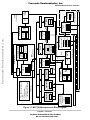
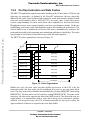
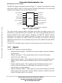
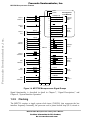
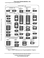
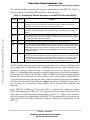
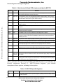
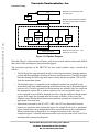

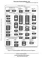
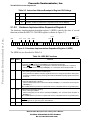
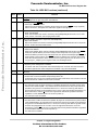
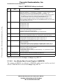
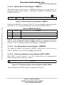
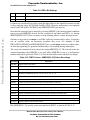
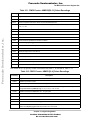
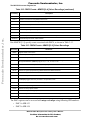
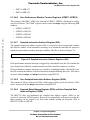
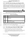
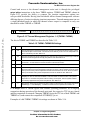
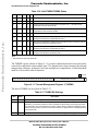
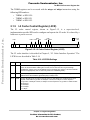
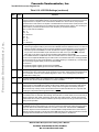
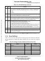
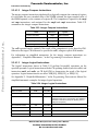
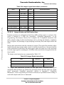
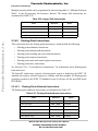
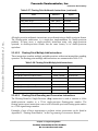
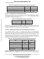
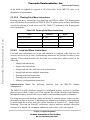
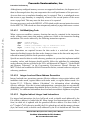
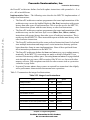
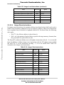
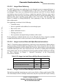
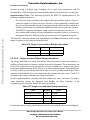
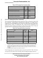
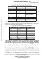
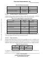
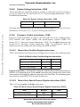
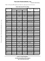
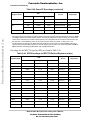
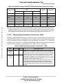
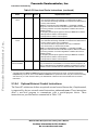
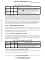
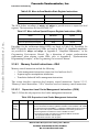
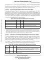
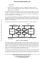
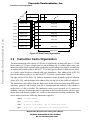
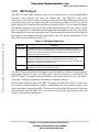
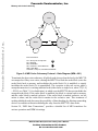
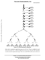
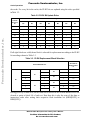
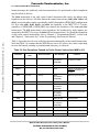
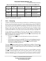
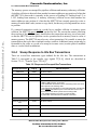
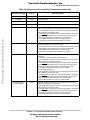
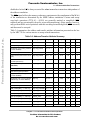
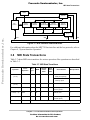
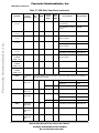
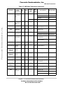
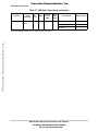
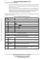
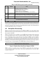
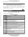
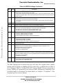
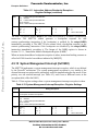
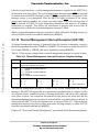

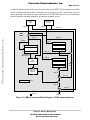
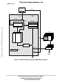
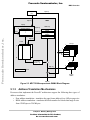
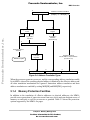
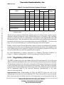
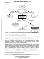
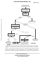
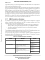
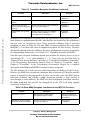
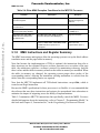
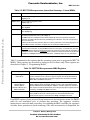
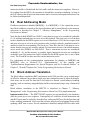
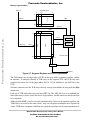
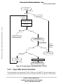
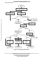
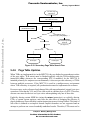
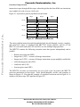
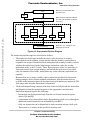
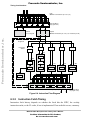
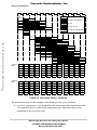
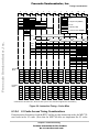
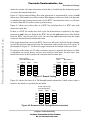
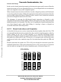
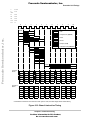
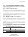
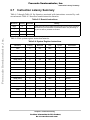
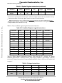
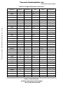
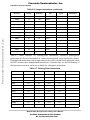
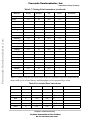
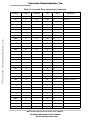
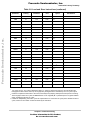

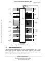
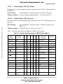
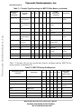
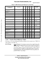
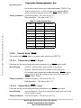
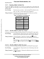
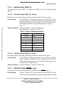
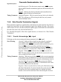
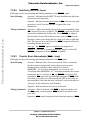
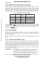
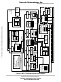
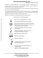
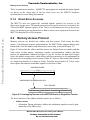
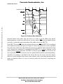
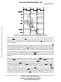
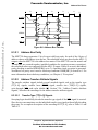
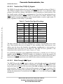
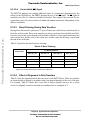
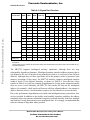
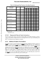
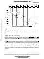
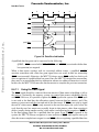
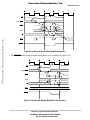
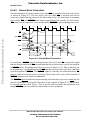
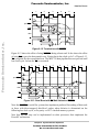
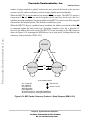
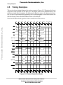
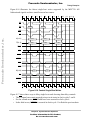
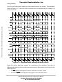
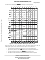
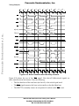
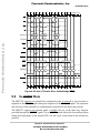

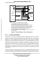
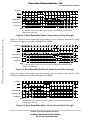
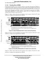
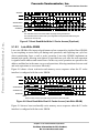
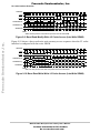
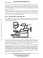
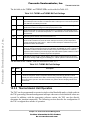
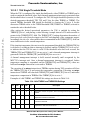
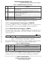
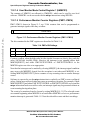
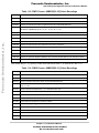
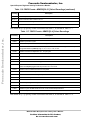
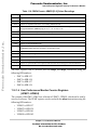
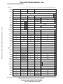
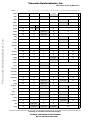
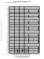
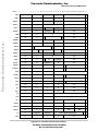
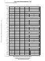
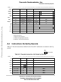
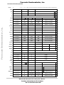
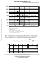
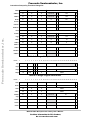
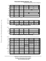
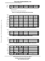
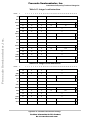
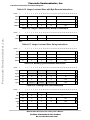
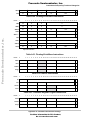
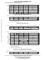
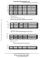
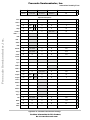
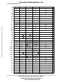
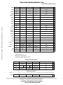
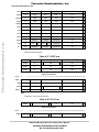
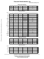
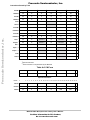
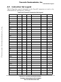
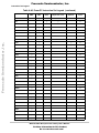
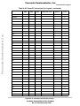
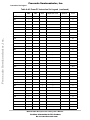
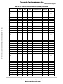
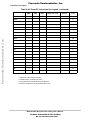
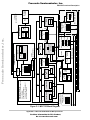
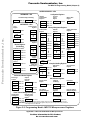
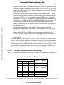
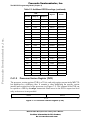
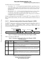
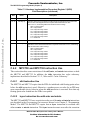
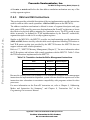
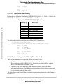
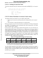
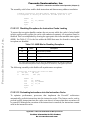
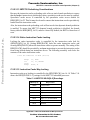
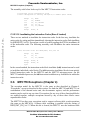
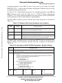
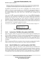
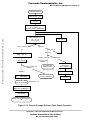
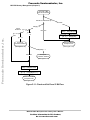
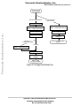
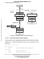
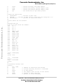
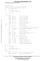
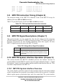
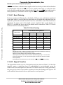
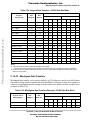
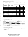
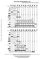
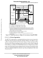
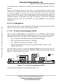
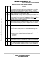
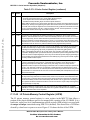
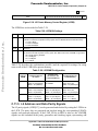
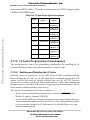
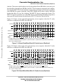
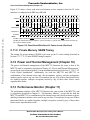
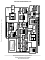
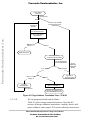
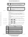


![PC755BM8 [Preliminary]](http://vs1.manualzilla.com/store/data/005786860_1-ac3ee01c2b00aeb18fc7f0a57a841c91-150x150.png)