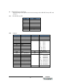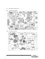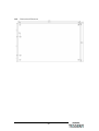
1
TS-R-IN32M3-CL
User Manual
(R-IN32M3-CL Evaluation Board)
Issued: October 1, 2013 (Version 1.1)
Tessera Technology Corporation
TS-TUM01739W
This board is for research and development.
・
The content of this document is subject to change without prior notice.
・
The evaluation board described in this document is made available for research and
development.
・
This information contained herein may not be reprinted or duplicated without written notice
from Tessera Technology, Inc. (Tessera).
・
Tessera does not guarantee or grant licenses to the intellectual property or other rights of
Tessera or any third party for use of this material or the products described in this document.
Tessera does not bear any responsibility if a problem occurs related to the ownership rights of
third parties arising from the use of the above-described products or information.
・
The information contained in this document is intended to illustrate the operation of
semiconductor products and application examples. Therefore, customers using this
information in the design of their own equipment must take full responsibility for product
design. Tessera shall not be liable for any damage caused to the customer or any third parties
DECLARAT10N OF CONFORMITY
We,Product Compliance Division
TESSERATECHNOLOGYINC.
4,2710-l NoboHto,Tama― ku,Kawasaklcitt Kanagawa 214-0014」
Phonet+81-44-271-7533
APAN
Faxi+81瑠 -271-7534
declare under our sole responsibility thatthe product
Producti Board test systems
Modeli
Ts_R― IN32M3-CL Evalua8on Board
to which this declara8on relates is in conformity wtth the following standards of other
norrnalive documents
EN 61326-1:2013(BasiC immunity test requirements)
IEC 61000-4-2:2008住 4kV contact dischatte/± 8kV air discharge)
IEC 61000-4-3:2006+Al:2007+A2:2010(80-1000Mhz,leve1 2(3V/m)/
14-2.OGHz,leve1 2(3V/m)/2.0-217GHz,leve1 1(lV/m))
IEC 61000:4-5i2005(± 0.5kV DC pOwver portiline to line/
±1 0kV DC povver pOrtiline to earth/
±1 0kV Signalpo代 :line to ealth)
IEC 61000i4-4:2004+Al:2010(Signal portsi±
1.Okヽ
IEC 61000:4-6:2008 1AC powver portsileve1 2(3`
つ
の)
IEC 61000:4-8i2009(3A/m50 Hz,60Hz)
CiSPR ll:2009+Al:2010Group l ClassARadiatedemission(30 MHz-1,O GHz)
following the provislons of EC Council Directive
EMC Directive 2004/108/EC
AuthoHzed RepresentaJve
Signaturei
Hitoshi Attmoto
TESSERATECHNOLOGYINC.
The president
Dtte ofに sueL_夕
θ●
考θ
と
er./,2ク β
TS― TER01832
Revision history
Version
Ver. 1.0
Vwe.1.1
Date
Aug 1, 2013 Initial version
Description
Oct 1,2013 research and development Only Insert
DECLARATION OF CONFORMITY Insert
目 次
1. Application.................................................................................................................................................. 1
2. Overview..................................................................................................................................................... 1
3. Specification................................................................................................................................................ 2
4. External View............................................................................................................................................. 3
4.1. Board Component Side.............................................................................................................................3
4.2. Board Soldering Side ................................................................................................................................3
5. Section Names............................................................................................................................................ 4
5.1. Board Component Side.............................................................................................................................5
5.2. Board Soldering Side ................................................................................................................................5
6. Board Block Diagram................................................................................................................................ 6
7. Block Descriptions..................................................................................................................................... 7
7.1. R-IN32M3-CL ............................................................................................................................................7
7.2. Operation Mode Selection........................................................................................................................8
7.3. JTAG (ICE) Interface................................................................................................................................9
7.4. External Memory (Serial_Flash)......................................................................................................... 10
7.5. External Memory (Parallel_Flash)/External Host Interface......................................................... 10
7.6. I2C Interface.............................................................................................................................................11
7.7. CAN Interface ......................................................................................................................................... 12
7.8. CC-Link (Master/Slave) Interface....................................................................................................... 12
7.9. UART Interface....................................................................................................................................... 13
7.10. CC-Link IE (Giga-Ethernet) Interface............................................................................................. 14
7.11. Power Supply ........................................................................................................................................ 15
7.12. Reset........................................................................................................................................................ 16
7.13. Clocks...................................................................................................................................................... 17
7.14. Port Controls ......................................................................................................................................... 18
8. DIP, Rotary, and Push Switch Configurations..................................................................................... 19
8.1. SW1: Mode Setting................................................................................................................................. 19
8.2. DIP-SW SW23: DIP Switch for CC-Link Initialization Setting.................................................... 20
8.3. SW24: DIP Switch for CC-Link (Slave) Initialization Setting....................................................... 20
8.4. SW17/SW20: Rotary Switches (2) for CC-Link Station Number Setting ................................... 21
8.5. SW22: Rotary Switch for CC-Link (Master) Baud Rate Setting .................................................. 22
8.6. SW21: Rotary Switch for CC-Link (Slave) Baud Rate Setting...................................................... 22
8.7. SW18/SW19: Rotary Switches (2) for CC-Link IE Station Number Setting.............................. 23
8.8. SW15/SW16: Push switches (2) for Reset.......................................................................................... 23
9. LED........................................................................................................................................................... 24
9.1. Power Supply........................................................................................................................................... 24
9.2. LEDs for CC-Link IE Station Display................................................................................................ 24
9.3. LEDs for Monitoring CC-Link IE Operations.................................................................................. 24
9.4. LEDs for CC-Link (Master/Slave) Monitoring Operations............................................................ 25
9.5. LED for External Host Switch Display.............................................................................................. 25
9.6. LEDs for Monitoring UART (USB) Communications .................................................................... 25
9.7. LEDs for Monitoring CC-Link IE Communications ....................................................................... 26
10. Connector Pin Definitions .................................................................................................................... 26
10.1. I2C Connector ....................................................................................................................................... 26
10.2. CAN Connector..................................................................................................................................... 27
10.3. UART (USB) Connector...................................................................................................................... 27
10.4. CC-Link IE (Giga-Ethernet) Connector........................................................................................... 28
10.5. JTAG (ICE) Connector........................................................................................................................ 29
10.6. CC-Link Connector.............................................................................................................................. 29
10.7. DC Power Jack ..................................................................................................................................... 30
10.8. Power Connector .................................................................................................................................. 30
10.9. External memory/MCU Connector .................................................................................................. 31
10.10. CC-Link IE Monitor Connector....................................................................................................... 34
10.11. CC-Link Monitor Connector............................................................................................................ 34
10.12. Test Monitor Connector .................................................................................................................... 35
11. Table of Unused Pins and Pad Connection Pins................................................................................ 36
11.1. Unused Pins .......................................................................................................................................... 36
11.2. PAD Connection Pins .......................................................................................................................... 36
11.3. Test Pins................................................................................................................................................. 37
11.4. Universal Pad ....................................................................................................................................... 37
12. Jumper Settings .................................................................................................................................... 38
12.1. External Memory (Parallel_Flash) Pins.......................................................................................... 38
12.2. CC-Link IE PHY Reset Pins.............................................................................................................. 38
12.3. CC-Link IE LED Pins ......................................................................................................................... 39
12.4. CC-Link LED Pins............................................................................................................................... 39
12.5. CC-Link Connector Terminal Pins ................................................................................................... 40
12.6. CC-Link Operating Mode Pins.......................................................................................................... 40
12.7. CC-Link Power Supply Pin................................................................................................................ 41
12.8. CC-Link Power Debug Pins............................................................................................................... 41
12.9. CC-Link Port Operation Pins ............................................................................................................ 42
12.10. I2C-ch1 Pins........................................................................................................................................ 42
12.11. CAN Pins............................................................................................................................................. 43
12.12. CAN Power Supply Pin .................................................................................................................... 43
12.13. WDTZ(CC-Link) Pin ......................................................................................................................... 44
12.14. CC-Link Interrupt Selection Pins................................................................................................... 44
12.15. CC-Link IE Interrupt Connection Pin........................................................................................... 45
12.16. External Reset Connection Pins ..................................................................................................... 45
13. Default Factory Settings....................................................................................................................... 46
13.1. DIP-SW/Rotary-SW............................................................................................................................. 46
13.2. Jumpers.................................................................................................................................................. 46
13.3. MAC Address ........................................................................................................................................ 47
14. Board External Diagram...................................................................................................................... 48
14.1. Board Component Side ....................................................................................................................... 48
14.2. Board Soldering Side........................................................................................................................... 48
14.3. Dimensional Diagram......................................................................................................................... 49
1.
Application
This user’s manual provides explanations for use of the TS-R-IN32M3-CL Evaluation Board.
Applicable board version: TS-R-IN32M3-CL_002
2.
Overview
The R-IN32M3-CL board was developed for evaluating the R-IN32M3-CL device and offers the
following interfaces:
・ Giga-Ethernet (CC-Link IE)
・ CC-Link (Master/Slave)
・ UART (USB mini-B)
・ I2C
・ CAN
・ External memory (Serial_Flash /Parallel_Flash)
・ External memory/MCU interface
・ JTAG (ICE_I/F)
・ Others, such as switches and LEDs
This board specification does not support the following combinations:
・ CC-Link IE and CC-Link (Slave)
・ CC-Link (Master) and CC-Link (Slave)
・ CC-Link (Master/Slave) and CAN (ch0)
・ CC-Link IE and CAN (ch0, ch1)
・ CC-Link (Master/Slave) and I2C (ch1)
* CC-Link (Master): indicates master station, local station, and intelligent device station
* CC-Link (Slave): indicates remote device station
* CC-Link (Master) will be supported in the future.
Note: The CC-Link/CC-Link IE circuits on this board do not meet conformance
requirements.
1
3.
Specification
Item
Specification
Renesas Electronics System LSI "R-IN32M3-CL"
Main ASSP *1 ARM CortexTM-M3 32-bit RISC CPU with HW-RTOS (Hardware Real-Time OS)
1.3M-byte RAM large-capacity Operating frequency 100MHz
Flash memory (Serial)
64Mbit, S25FL064P0XNFI001 equivalent
Ext. Memory
Flash memory (Parallel)
128Mbit (8Mx16bit), S29GL128S10TFI010 equivalent
I2C
2Ch
4 × 1 pin 2.54mm header
External Host MCU
1Ch
50 × 2 pin 0.6mm connector
USB mini-B connector *2
UART
1Ch ( UART to USB )
USB-Ver2
CAN
CAN transceiver
1Ch
(±80V Fault protection
4 × 1 pin 2.54mm header
Interface
Up to 1Mbps)
RJ-45
CC-Link IE
2Ch
Giga-Ethernet Ext' PHY
1Ch
CC-Link
35605-5153-B00 PE equivalent
(Master or Slave)
20-pin half-pitch connector
JTAG(ICE)
1Ch
(Trace supported)
Power Supply
1 red LED
Giga-Ethernet Monitor
4 red and yellow LEDs per Ch
CC-Link Monitor
8 red and green LEDs
LED
CC-Link IE Code Monitor
9 green LEDs
CC-Link IE Monitor
9 red and green LEDs
Ext. MCU interface selection 1 green LED
UART(Tx/Rx)
2 green LEDs
Operation mode selection
8 bits (SW1)
CC-Link channel selection
2 rotary switches (SW17 and SW20)
CC-Link IE channel selection 2 rotary switches (SW18 and SW19)
CC-Link (Master)
1 rotary switch (SW22)
DIP-SW/
Baud rate selection
Rotary-SW
CC-Link (Slave)
1 rotary switch (SW21)
Baud rate selection
CC-Link (Slave)
3 bits (SW24)
Initial value set
CC-Link IE Initial value set
4 bits (SW23)
Power Supply
AC Adapter
+5.0V +/- 5%, 2A or more (center plus)
Operation Temp. 0 to +70o
*1 -- ASSP means “Application Specific Standard Product,” a standard System LSI. Please refer to the
Renesas datasheet and user’s manual for details concerning R-IN32M3-CL.
*2 -- The USB cable must be inserted and detached while the board is powered.
2
4.
External View
The following are photos outlining the board’s exterior.
4.1.
Board Component Side
4.2.
Board Soldering Side
3
5.
Section Names
The following photos provide coordinates and labels to help locate specific positions on the
board when referred to later in this document.
4
Board Component Side
3
4
5
6
SW24
CC-Link(Slave)
Initial
Selection
CC-Link
LED
SW22
CC-Link(Master)
Baud Rate
Selection
SW1
Mode
CN1
Selection
ICE Connector
7
8
9
CN8/CN10
I2C Connector
10
11
CN18
CN18
USB-Mini-B
CN11
CAN Connector
I
2
SW21
CC-Link(Slave)
Baud Rate
Selection
H
I
1
D37:
37:TxLED
D38:
38:RxLED
H
5.1.
CN13
G
PHY1
GND
2.5V
CN6
CN6/CN5
CN5
RJ45
RJ45
Connector
1.2V
E
J1
J16
1.0V
J17
J18
J19
CN4
D
GND
J6
J7
D
E
J2
J4
PHY0
R-IN32M3-CL
CN2
Ext
MCU
Connector
CN7
CN7
CC-Link
Connector
CN20
J30
C
J11
J10
J12
5.0V
J31
J8
J9
C
CL5.0V
CC-Link IE
Channel
LED
F
F
J3
J5
J28
J13
J14
J25
CN14
J16
J15
J24
J23
3.3V
J27
SW20/SW17
CC-Link
Channel
Selection
J20
J21
J22
G
GND
GND
B
B
FG
1
5.2.
2
3
CC-Link IE
LED
SW23
CC-Link IE
Initial
Selection
4
CN19
Power
Connector
SW15/SW16
ResetSW
5
6
7
8
Power LED
CN12
DC Power
9
A
A
SW18/SW19
CC-Link IE
Channel
Selection
10
11
Board Soldering Side
3
4
5
6
7
8
9
10
11
10
11
H
G
G
H
I
2
I
1
F
E
E
F
Serial
FLASH
D
C
B
A
A
B
C
D
Parallel
FLASH
1
2
3
4
5
6
5
7
8
9
Board Block Diagram
6.
AC Adapter
(+5V)
Serial Flash
ROM I/F
Serial Flash ROM
(64Mbit)
DC Jack
-
Parallel Flash
ROM I/F
+
Parallel Flash ROM
(8M x 16bit)
100pin
Connecter
Ext. MCU I/F
DC/DC
5.0V⇒3.3V(2A)
Digital system 3.3V
DC/DC
5.0V⇒1.0V(2A)
Digital system 1.0V
FB
Analog system 1.0V
DC/DC
5.0V⇒1.2V(2A)
for PHY 1.2V
DC/DC
5.0V⇒2.5V(2A)
for PHY 2.5V
Isolated
DC/DC
3.3V⇒5.0V
for CC-Link
EtherPHY0 I/F
(MDI0)
PHY
RJ45 Connecter
(Trans Inside)
EtherPHY1 I/F
(MDI1)
PHY
RJ45 Connecter
(Trans Inside)
UART I/F
UART to USB
Driver
USB (mini-B)
RS485 Driver
other
CC-Link
Connecter
CAN
Driver
Pin Header
(4pin)
CC-Link 5.0V
Master/Slave
CC-Link I/F
CAN I/F
OSC
25MHz
XT2
OSC
80MHz
Dedicated for CC-Link
OSC
2.097MHz
Dedicated for CC-Link
Pin Header
2ch (4pin)
I2C I/F
(ch0/ch1)
CLK80M
LED 8 bits (CC-Link)
CLK2_097M
LED 9 bits (CC-Link IE)
RESET-SW
Reset IC
HOTRESETZ
LED 9 bits (Station Number)
RESET-SW
DIP-SW
DIP-SW 4 bits (CC-Link IE Initial value)
Wired_or
Reset IC
(PowerON)
Reset IC
DIP-SW
RESETZ
DIP-SW 4 bits (CC-Link_Slave Initial value)
TRSTZ
⇒
JTAG(ICE)
20-pin Connector
(Half Pitch)
Rotary SW (0 to 9) x 4
⇒
0
Rotary SW (0 to F) x 2
JTAG(ICE)
0
DIP-SW (8 bits)
Operation Mode
Selection Pins
Monitor
Pin Header
6
7.
7.1.
Block Descriptions
R-IN32M3-CL
Refer to the corresponding Renesas Electronics Corp. datasheet and user’s manual
for more details.
7
7.2.
Operation Mode Selection
An 8-bit DIP switch (DIP-SW1) is provided for operation mode selections.
+3.3V
R-IN32M3-CL
1
BOOT1
2
BOOT0
3
MEMIFSEL
4
FRU2(MEMCSEL)
5
BUS32EN
6
HIFSYNC
7
FRU1(ADMUXMODE)
8
HWRZSEL
Pull Down
Registar
8
7.3.
JTAG (ICE) Interface
The JTAG (ICE) connector is available for the on-board CPU, R-IN32M3-CL.
The connector is a 10 x 2 pin header with1.27 mm pitch.
*To avoid incorrect insertion, the 7th pin is pulled out.
*Signal TRSTZ is wired-OR connected to signal RESETZ pin.
9
7.4.
External Memory (Serial_Flash)
A serial flash memory (S25FL064P0XNFI010 equivalent) is used to boot the internal
CPU.
+3.3V
S25FL064P0XNFI010
equivalent
R-IN32M3-CL
7.5.
+3.3V
W#ACC/IO2
P14 SMSCK
P17 SMCSZ
SCK
P16 SMSO
P15 SMSI
SI/IO0
CS#
SO/IO1
HOLD#/IO3
External Memory (Parallel_Flash)/External Host Interface
A parallel flash memory (S29GL128S10TFI010 equivalent) is mounted for the external
memory.
A 100-pin header (CN3) is provided for interface with the external host MCU.
DIP-SW (SW1) selects either external memory interface CSZ0 or external host
interface HCSZ/HPGSCSZ, exclusively.
10
7.6.
I2C Interface
R-IN32M3-CL is connected to the header, enabling I2C sync communications (2
channels).
A 4 x 1 pin header (2.54mm pitch) is available for I2C interface.
11
7.7.
CAN Interface
The board offers a CAN driver and pin header, supporting CAN communication.
A 4 x 1 pin header (2.54mm pitch) is available for CAN interface.
*CAN interface cannot be used during CC-Link IE communications.
7.8.
CC-Link (Master/Slave) Interface
The board offers isolators, RS485 transceivers, and filters, supporting CC-Link
(Master/Slave) communication.
Connector 35610-5153-B00-PE is also mounted on the board.
*Use a jumper to set communication to Master or Slave.
12
7.9.
UART Interface
The board offers a UART-to-USB chip for the UART0 function (FT232RQ) and a
USB connector, supporting PC communication in asynchronous mode.
A USB mini-B connector is mounted for UART interface.
13
7.10.
CC-Link IE (Giga-Ethernet) Interface
The board is equipped with an on-chip Ethernet PHY (88E1111-B2-BAB1C000)
for CC-Link IE communication. The external connector consists of 2 channels of
RJ45 which embed transformers.
88E1111-B2-BAB1C000
JF-01J-0-H22-020-2
“0” Clamp
ETH0_TXC
ETH0_GTXC
GTX_CLK
ETH0_TXEN
TX_EN
MDI3-
ETH0_TXER
TX_ER
MDI2+
TXD[7:0]
MDI2-
RX_CLK
MDI1+
MDI3+
ETH0_TXD[7:0]
ETH0_RXC
ETH0_RXDV
RX_DV
MDI1-
ETH0_RXER
RX_ER
MDI0+
RXD[7:0]
MDI0-
ETH0_RXD[7:0]
ETH0_CRS
CSR
ETH0_COL
COL
ETH0_GE_INT
INTN
MDC
MDIO
ETH_MDC
ETH_MDIO
88E1111-B2-BAB1C000
JF-01J-0-H22-020-2
ETH1_TXC
“0” Clamp
ETH1_GTXC
GTX_CLK
ETH1_TXEN
TX_EN
MDI3-
ETH1_TXER
TX_ER
MDI2+
TXD[7:0]
MDI2-
RX_CLK
MDI1+
ETH1_TXD[7:0]
ETH1_RXC
MDI3+
ETH1_RXDV
RX_DV
MDI1-
ETH1_RXER
RX_ER
MDI0+
RXD[7:0]
MDI0-
ETH1_RXD[7:0]
ETH1_CRS
CSR
ETH1_COL
COL
ETH1_GE_INT
INTN
MDC
MDIO
*Ethernet monitoring LEDs
Px_ERR
Px_LNK1000
Px_LNK100
Px_LNK10
Red LED
Yellow LED
Yellow LED
Yellow LED
14
7.11. Power Supply
DC 5V power is provided via the DC power jack and generates power for various
on-board devices.
The DC/DC converter array provides the following current capacities: 3.3V 2A (max),
1.0V 2A (max), 2.5V 2A (max), 1.2V 2A (max).
When 5.0V is supplied, LED_PWR (red) turns on.
The 5V power supply for CC-Link is generated through the isolated DC/DC via the
3.3V output.
The R-IN32M3-CL evaluation board also comes with a 5V power connector for
connections to other boards (the corresponding TS-R-IN32M3-CL).
15
7.12.
Reset
When the board is powered, push the reset button (SW15/SW16) or apply a reset
signal via the ICE connector, to reset all board resources.
During the power-on reset, the on-chip redundancy RAM is also reset.
The board also provides jumpers to apply external resets via the external host
interface connector.
* During Power ON, PONRZ must be 20ms LOW, and RESETZ and HOTRESETZ
must be 40ms LOW.
* Push Switch must apply at least 20ms LOW.
16
7.13.
Clocks
This evaluation board provides the following clocks: R-IN32M3-CL system clock (25
MHz), CC-Link clock (80 MHz), and CC-Link IE clock (2.097152 MHz).
*Oscillation stabilization period for each oscillator: 10ms.
17
7.14.
①
②
②
④
⑤
⑥
⑦
Port Controls
DIP-SW (CHS-04TB equivalent) is provided for the CC-LINK IE initial mode
setting.
LED (9-bit) is provided for displaying the CC-Link IE station number.
One rotary switch (SC-1110/SC-2110 equivalent) is provided for each CC-Link IE
station number setting.
Rotary switch (SC-1110) is provided for the CC-Link (Master) baud rate setting.
Rotary switch (SC-2110) is provided for the CC-Link (Slave) baud rate setting.
DIP-SW (CH-04TB) is provided for the CC-Link (Slave) initialization setting.
Two rotary switches (SC-2110 equivalent) are provided for the CC-Link station
number settings.
18
8.
8.1.
DIP, Rotary, and Push Switch Configurations
SW1: Mode Setting
Location: H-4
Board Silk: SW1
Part #: COPAL CHS-08TB (or equivalent part)
SW1 is an 8-bit DIP switch connected to the I/O ports of the R-IN32M3-CL chip.
This switch defines the operation mode of the chip.
SW1
Level
Pin Name
Boot Mode Selection
2
1
H H
Instruction Ram Boot (Debug only)
L
H BOOT0 Ext. MCU Boot
H
L BOOT1 Ext. Serial Flash ROM Boot
L
L
Ext. Memory Boot
2
ON
ON
OFF
OFF
1
ON
OFF
ON
OFF
SW1
3
OFF
ON
SW1
4
OFF
ON
SW1
5
OFF
ON
SW1
6
OFF
ON
SW1
7
OFF
ON
SW1
8
OFF
ON
Level
Pin Name
L
H
MEMIFSEL
Level
Pin Name
L
H
FRU2
(MEMCSEL)
Level
Pin Name
L
H
BUS32EN
Level
Pin Name
L
H
HIFSYNC
Level
Pin Name
L
H
Level
L
H
Ext. Memory I/F Type Selection
Slave Memory I/F
Ext. MCU I/F
Ext. Memory Controller Setting
Asynchronous SRAM MEMC
Synchronous burst access MEMC
Ext. Memory I/F Bus Width Selection
16-bit Bus
32-bit Bus
Ext. MCU I/F Operation Mode Selection
Asynchronous SRAM Interface
Synchronous SRAM Interface
Ext. Memory I/F Address MUX Selection
FRU1
Connect in parallel
(ADMUXMODE) Address bus is MUXed on data bus
Ext. MCU I/F
Pin Name
HWRZ/HBENZ Selection
HBENZ is selected
HWRZSEL
HWRZ is selected
19
8.2.
DIP-SW SW23: DIP Switch for CC-Link Initialization Setting
Location: B-5
Board Silk: SW23
Part #: COPAL CHS-04TB (or equivalent part)
SW23 is a 4-bit DIP switch connected to the I/O ports of the R-IN32M3-CL chip.
This switch sets the initial values for the CC-Link IE.
Pin #
1
2
3
4
8.3.
R-IN32M3-CL
Pin Name
P32
P33
P34
RP17
Signal Name
CCI_MON1_GMIIO
CCI_WAITEDGEH
CCI_WRLENH
CCI_MON0_GMIIBUFH
SW24: DIP Switch for CC-Link (Slave) Initialization Setting
Location: H-3
Board Silk: SW24
Part #: COPAL
CHS-04TB (or equivalent part)
SW24 is a 4-bit DIP switch connected to the I/O ports of the R-IN32M3-CL chip.
This switch sets the initial values for the CC-Link (Slave).
*The 4th bit is left open.
SW24
ON
1 2 3 4
Pin #
1
2
3
4
R-IN32M3-CL
Pin Name
P22
P23
P24
Open
20
Signal Name
CCS_IOTENSU
CCS_SENYU0
CCS_SENYU1
-
8.4.
SW17/SW20: Rotary Switches (2) for CC-Link Station Number Setting
Location: F-3
Board Silk: SW17、SW20
Part #: COPAL
SC-2110 (or equivalent part)
SW17 and SW20 are real code 10-position rotary switches connected to the I/O
ports of the R-IN32M3-CL chip.
These switches set the station numbers for the CC-Link.
SW17
SW
Code
0
SW17
SW
1
2
4
8
2
3
●
● ●
Code
1
2
4
8
Position
4 5 6 7
●
●
● ●
● ● ● ●
8
9
●
● ●
0
SW20
1
●
SW20
1
●
2
3
●
● ●
Position
4 5 6 7
●
●
● ●
● ● ● ●
8
9
●
● ●
21
R-IN32M3-CL
Pin Name
P74
P75
P76
P77
R-IN32M3-CL
Pin Name
P70
P71
P72
P73
8.5.
SW22: Rotary Switch for CC-Link (Master) Baud Rate Setting
Location: F-4
Board Silk: SW22
Part #: COPAL
SC-1110 (or equivalent part)
SW22 is a real code 16-position rotary switch connected to the I/O ports of the
R-IN32M3-CL chip.
This switch sets the baud rate for the CC-Link (Master).
SW22
SW
Code
0
SW22
1
2
4
8
2
3
●
● ●
Position
7 8 9 A B C D E F
●
●
●
●
●
● ●
● ●
● ●
● ● ● ●
● ● ● ●
● ● ● ● ● ● ● ●
4
5
●
6
R-IN32M3-CL
Pin Name
P62
P63
P64
P65
SW21: Rotary Switch for CC-Link (Slave) Baud Rate Setting
Location: F-4
Board Silk: SW21
Part #: COPAL
SC-2110 (or equivalent part)
SW21 is a real code 10-position rotary switch connected to the I/O ports of the
R-IN32M3-CL chip.
This switch sets the baud rate for the CC-Link (Slave).
SW21
9 0 1
⇒
7 8
2 34
6
8.6.
1
●
5
SW
Code
0
SW21
1
2
4
8
1
●
2
3
●
● ●
Position
4 5 6 7
●
●
● ●
● ● ● ●
8
9
●
● ●
22
R-IN32M3-CL
Pin Name
RP02
RP03
RP04
RP05
8.7.
SW18/SW19: Rotary Switches (2) for CC-Link IE Station Number Setting
Location: B-3
Board Silk: SW18、SW19
Part #: COPAL
SC-1110 / SC-2110 (or equivalent)
SW18 and SW19 are real code 16/10-position rotary switches connected to the I/O
ports of the R-IN32M3-CL chip.
These switches set the station numbers for the CC-Link IE.
SW19
SW18
0
0 1
8
5
SW
Code
0
SW19
1
2
4
8
SW
Code
1
●
0
SW18
8.8.
1
2
4
8
1
●
2
3
●
● ●
2
3
●
● ●
Position
7 8 9 A B C D E F
●
●
●
●
●
● ●
● ●
● ●
● ● ● ●
● ● ● ●
● ● ● ● ● ● ● ●
4
5
●
6
Position
4 5 6 7
●
●
● ●
● ● ● ●
8
9
●
● ●
R-IN32M3-CL
Pin Name
RP12
RP13
RP14
RP15
R-IN32M3-CL
Pin Name
RP06
RP07
RP10
RP11
SW15/SW16: Push switches (2) for Reset
Location: B-5/B-6
Board Silk: SW15, SW16
Part #: COPAL
SKQMBBE010 (or equivalent)
SW15 and SW16 are tact switches (PUSH-SW) connected to the I/O ports of the
R-IN32M3-CL chip.
These switches are used to input resets (RESETZ/HOTRESETZ).
*SW15 is for RESETZ, SW16 is for HOTRESETZ.
23
9.
9.1.
LED
Power Supply
Location: B-9
Board Silk: LED_PWR
Part #: STANLAY BR1111C (or equivalent part)
This is a red LED (1 bit) for monitoring the power supply.
9.2.
LEDs for CC-Link IE Station Display
Location: C-3
Board Silk: See list below
Part #: STANLAY PG1111C (or equivalent part)
These are green LEDs (9 bits) for displaying the CC-Link IE station number.
*The LED turns on when the signal is LOW.
・
・
・
・
・
・
・
・
・
9.3.
KYOKU_1
KYOKU_2
KYOKU_4
KYOKU_8
KYOKU_10
KYOKU_20
KYOKU_40
KYOKU_80
KYOKU_100
(Green)
(Green)
(Green)
(Green)
(Green)
(Green)
(Green)
(Green)
(Green)
LEDs for Monitoring CC-Link IE Operations
Location: B-4
Board Silk: See list below
Part #: STANLAY BR1111C / PG1111C (or equivalent part)
These are green LEDs (9 bits) for monitoring CC-Link IE operations.
*The LED turns on when port is set to Low.
・
・
・
・
・
・
・
・
・
IE_RUN
IE_DLNK
IE_ERR
IE_LERR1
IE_LERR2
IE_SD
IE_RD
IE_REM
IE_MODE
(Green)
(Green)
(Red)
(Red)
(Red)
(Green)
(Green)
(Green)
(Green)
24
9.4.
LEDs for CC-Link (Master/Slave) Monitoring Operations
Location: G-3
Board Silk: See list below
Part #: STANLAY BR1111C/PG1111C (or equivalent part)
These are red/green LEDs (8 bits) for monitoring CC-Link (Master/Slave)
operations.
*The LED turns on port is set to Low.
・
・
・
・
・
・
・
・
9.5.
CC_LERR
CC_ERR
CC_RUN
CC_MST
CC_LRUN
CC_RD
CC_SD
CC_SMST
(Red)
(Red)
(Green)
(Red)
(Red)
(Red)
(Green)
(Green)
For Master or Slave use
For Master use only
For Master or Slave use
For Master use only
For Master or Slave use
For Master or Slave use
For Master or Slave use
For Master use only
LED for External Host Switch Display
Location: H-4
Board Silk: HOST
Part #: STANLAY PG1111C (or equivalent part)
This green LED displays the external host switch.
This LED lights up when pin 3 (MEMIFSEL) of SW1 (DIP-SW) is ON.
9.6.
LEDs for Monitoring UART (USB) Communications
Location: H-9
Board Silk: RX/TX
Part #: STANLAY PG1111C (or equivalent part)
These green LEDs (2 bits) are for monitoring the UART (USB) communication
operations.
25
9.7.
LEDs for Monitoring CC-Link IE Communications
Location: D-9/F-9/G-9
Board Silk: See list below
Part #: STANLAY BR1111C/AY1111C (or equivalent part)
These are red/yellow LEDs (4 bits per channel) for monitoring CC-Link IE
communications.
・ Px_ERR
・ Px_LINK1000
・ Px_LINK100
・ Px_LINK10
*x: indicates 0 or 1.
10.
10.1.
(Red)
(Yellow)
(Yellow)
(Yellow)
Connector Pin Definitions
I2C Connector
Location: H-6
Board Silk: CN8/CN10
Connector: 4x1pins, 2.54mm pin header
Part #: E-TEC
SL1-004-S116/01-55 (or equivalent part)
CN8
Pin #
1
2
3
4
CN10
I/O Dir.
I/O
I/O
-
Pin #
I/O Dir.
1
2
3
4
I/O
I/O
-
R-IN32M3-CL
Pin Name
P60
P61
R-IN32M3-CL
Pin Name
RP00
RP01
-
26
Signal Name
GND
SCL0
SDA0
+3.3V
Signal Name
GND
SCL0
SDA0
+3.3V
10.2.
CAN Connector
Location: H-7
Board Silk: CN11
Type: 4 x1pin header, 2.54mm pitch
Part #: E-TEC
SL1-004-S116/01-55 (or equivalent part)
CN11
Pin #
1
2
3
4
10.3.
I/O Dir.
I/O
I/O
-
Signal Name
GND
CANH
CANL
+3.3V or +5.0V
UART (USB) Connector
Location: H-9
Board Silk: CN18
Type: USB mini-B
Part #: molex
54819-0519 (or equivalent part)
CN18
Pin #
1
2
3
4
5
I/O Dir.
I/O
I/O
-
27
Signal Name
(VBUS)
(ID)
D+
DGND
10.4.
CC-Link IE (Giga-Ethernet) Connector
Location: E-10/G-10
Board Silk: CN5、CN6
Type: RJ-45 (built-in transistors), 2 units
Part #: JMCOMTECH JF-01J-0-H22-020-2 (or equivalent part)
CN5
Pin #
1
2
3
4
5
6
7
8
I/O Dir.
I/O
I/O
I/O
I/O
I/O
I/O
I/O
I/O
Signal Name
MX1+
MX1MX2+
MX3+
MX3MX2MX4+
MX4-
PHY Pin Name
MDI[0]+
MDI[0]MDI[1]+
MDI[2]+
MDI[2]MDI[1]MDI[3]+
MDI[3]-
CN6
Pin #
1
2
3
4
5
6
7
8
28
I/O Dir.
I/O
I/O
I/O
I/O
I/O
I/O
I/O
I/O
Signal Name
MX1+
MX1MX2+
MX3+
MX3MX2MX4+
MX4-
PHY Pin Name
MDI[0]+
MDI[0]MDI[1]+
MDI[2]+
MDI[2]MDI[1]MDI[3]+
MDI[3]-
10.5.
JTAG (ICE) Connector
Location: H-5
Board Silk: CN1
Type: 10 x 2 pin header, 1.27mm pitch
Part #: E-TEC SS2-19A-H70/0-55/11 (or equivalent part)
*To prevent incorrect insertion, the 7th pin has been removed.
CN1
Pin #
I/O Dir.
Signal Name
1
2
3
4
5
6
7
8
9
10
Output
Output
Output
Input
Output
(Vtref)
TMS
GND
TCK
GND
TDO
TDI
GND
nRESET
10.6.
R-IN32M3-CL
Pin Name
TMS
TCK
TDO
TDI
TRSTZ
Pin #
I/O Dir.
Signal Name
11
12
13
14
15
16
17
18
19
20
Input
Input
Input
Input
Input
TgrPwr
TRACECLK
TgrPwr
TRACEDATA0
GND
TRACEDATA1
GND
TRACEDATA2
GND
TRACEDATA3
CC-Link Connector
Location: C-10
Board Silk: CN7
Type: 5-pin power clamp, board mount header
Part #: 3M 35605-5153-B00 PE
CN7
Pin #
1
2
3
4
5
I/O Dir.
I/O
I/O
-
29
Signal Name
DA
DB
DG
SLD
R-IN32M3-CL
Pin Name
TRACECLK
TRACEDATA0
TRACEDATA1
TRACEDATA2
TRACEDATA3
10.7.
DC Power Jack
Location: B-9
Board Silk: CN12
Type: DC power jack
Part #: HOSIDEN HEC0470-01-630 (or equivalent part)
10.8.
D = φ2.0
Power Connector
Location: B-8
Board Silk: CN19
Type: 2 x 1pin header, 2.54mm pitch
Part #: morex 22-11-2022 (or equivalent part)
CN19
Pin #
1
2
I/O Dir.
-
30
Signal Name
+5.0V
GND
10.9.
External memory/MCU Connector
Location: D-2
Board Silk: CN3
Type: 50 x 2 pin header, 0.6mm pitch
Part #: HRS FX8C-100P-SV1(92) (or equivalent part)
CN3
31
●When using connector as external memory interface
Pin #
I/O Dir.
Signal Name
Pin #
I/O Dir.
1
+3.3V
2
3
Output P40(A1)
4
Output
5
Output A3
6
Output
7
Output A5
8
Output
9
Output A7
10
Output
11
Output A9
12
Output
13
Output A11
14
Output
15
Output A13
16
Output
17
Output A15
18
Output
19
Output A17
20
Output
21
Output A19
22
Output
23
GND
24
25
I/O
D0
26
I/O
27
I/O
D2
28
I/O
29
I/O
D4
30
I/O
31
I/O
D6
32
I/O
33
I/O
D8
34
I/O
35
I/O
D10
36
I/O
37
I/O
D12
38
I/O
39
I/O
D14
40
I/O
41
GND
42
43
Output WRSTBZ
44
Input
45
Input P45(WAITZ1) *2
46
Output
47
Input P46(WAITZ2) *2
48
Input
49
Output P42(HERROUTZ) *2
50
Output
51
Input P47(WAITZ3) *2
52
Input
53
Output RDZ
54
Output
55
Output RP21(A21)
56
I/O
57
Output RP23(A23)
58
I/O
59
GND
60
61
Output RP24(A24)
62
I/O
63
Output RP22(A22)
64
I/O
65
Output RP25(A25)
66
I/O
67
Output RP27(A27)
68
I/O
69
Output RP26(A26)
70
I/O
71
Output RP20(BCYSTZ)
72
I/O
73
I/O
RP30(D24)
74
I/O
75
I/O
RP32(D26)
76
I/O
77
I/O
RP33(D27)
78
I/O
79
I/O
RP31(D25)
80
I/O
81
Output P51(CSZ2)
82
I/O
83
GND
84
85
Output P50(CSZ3)
86
I/O
87
Output RP07(WRZ3/BENZ3)
88
Output
89
Output RP06(WRZ2/BENZ2)
90
Output
91
I/O
RP05 *2
92
Output
93
I/O
RP04 *2
94
I/O
95
Output CSZ0(244) *1
96
Output
97
I/O
RP03 *2
98
Output
99
+3.3V
100
Input
*1: The signal is output through 74S244.
*2: The signal is not used.
32
Signal Name
+3.3V
A2
A4
A6
A8
A10
A12
A14
A16
A18
A20
GND
D1
D3
D5
D7
D9
D11
D13
D15
GND
P43(HBUSCLK) *2
RSTOUTZ *2
NMIZ *2
WRZ0/BENZ0
P41(WAITZ)
WRZ1/BENZ1
RP34(D28)
RP36(D30)
GND
RP35(D29)
RP37(D31)
RP10(D16)
RP11(D17)
RP12(D18)
RP13(D19)
RP14(D20)
RP15(D21)
RP16(D22)
RP17(D23)
RP01 *2
GND
RP00 *2
CSZ0 *2
P44(CSZ1) *2
CSZ1(244) *1
RP02 *2
HWRZSEL *2
BUSCLK
EXT_RSTINZ
●When using connector as external MCU interface
Pin #
I/O Dir.
Signal Name
1
+3.3V
3
Input P40(HA1)
5
Input A3
7
Input A5
9
Input A7
11
Input A9
13
Input A11
15
Input A13
17
Input A15
19
Input A17
21
Input A19
23
GND
25
I/O
HD0
27
I/O
HD2
29
I/O
HD4
31
I/O
HD6
33
I/O
HD8
35
I/O
HD10
37
I/O
HD12
39
I/O
HD14
41
GND
43
Input WRSTBZ(HWRSTBZ)
45
Output P45(WAITZ1) *2
47
Output P46(WAITZ2) *2
49
Output P42(HERROUTZ)
51
Output P47(WAITZ3) *2
53
Input RDZ(HRDZ)
55
Input RP21(A21) *2
57
Input RP23(A23) *2
59
GND
61
Input RP24(A24) *2
63
Input RP22(A22) *2
65
Input RP25(A25) *2
67
Input RP27(A27) *2
69
Input RP26(A26) *2
71
Input RP20(HBCYSTZ)
73
I/O
RP30(HD24)
75
I/O
RP32(HD26)
77
I/O
RP33(HD27)
79
I/O
RP31(HD25)
81
Input P51(CSZ2) *2
83
GND
85
Input P50(CSZ3) *2
87
Input RP07(HWRZ3/HBENZ3)
89
Input RP06(HWRZ2/HBENZ2)
91
I/O
RP05 *2
93
I/O
RP04 *2
95
Input CSZ0(244) *1 *2
97
I/O
RP03 *2
99
+3.3V
*1: The signal is output through 74S244.
*2: The signal is not used.
Pin #
2
4
6
8
10
12
14
16
18
20
22
24
26
28
30
32
34
36
38
40
42
44
46
48
50
52
54
56
58
60
62
64
66
68
70
72
74
76
78
80
82
84
86
88
90
92
94
96
98
100
33
I/O Dir.
Input
Input
Input
Input
Input
Input
Input
Input
Input
Input
I/O
I/O
I/O
I/O
I/O
I/O
I/O
I/O
Input
Output
Input
Input
Output
Input
I/O
I/O
I/O
I/O
I/O
I/O
I/O
I/O
I/O
I/O
I/O
I/O
I/O
I/O
Input
Input
Input
I/O
Output
Output
Input
Signal Name
+3.3V
A2
A4
A6
A8
A10
A12
A14
A16
A18
A20
GND
HD1
HD3
HD5
HD7
HD9
HD11
HD13
HD15
GND
P43(HBUSCLK)
RSTOUTZ *2
NMIZ *2
WRZ0(HWRZ0/HBENZ0)
P41(HWAITZ)
WRZ1(HWRZ1/HBENZ1)
RP34(HD28)
RP36(HD30)
GND
RP35(HD29)
RP37(HD31)
RP10(HD16)
RP11(HD17)
RP12(HD18)
RP13(HD19)
RP14(HD20)
RP15(HD21)
RP16(HD22)
RP17(HD23)
RP01 *2
GND
RP00 *2
CSZ0(HCSZ)
P44(HPGCSZ)
CSZ1(244) *1 *2
RP02 *2
HWRZSEL *2
BUSCLK *2
EXT_RSTINZ
10.10.
CC-Link IE Monitor Connector
Location: F-4
Board Silk: CN13
Type: 4 x 1 pin header, 2.54mm pitch
Part #: E-TEC
SL1-004-S116/01-55 (or equivalent part)
CN13
10.11.
Pin #
I/O Dir.
1
2
3
4
I/O
I/O
I/O
I/O
R-IN32M3-CL
Pin Name
P11
P12
P66
P67
Signal Name
CCI_SYNC
CCI_NMIZ
CCI_INTZ
CCI_CLKLOSSZ
CC-Link Monitor Connector
Location: F-3
Board Silk: CN14
Type: 7 x 1 pin header, 2.54mm pitch
Part #: E-TEC
SL2-014-S116/01-55 (or equivalent part)
CN14
Pin #
I/O Dir.
1
2
3
4
5
6
7
8
9
10
11
12
13
14
I/O
I/O
I/O
I/O
I/O
I/O
I/O
I/O
I/O
I/O
I/O
I/O
I/O
I/O
R-IN32M3-CL
Pin Name
P32
P33
P34
P11
P12
P02
P03
P04
P05
P06
P07
P10
P36
-
34
Signal Name
CCS_MON1
CCS_MON2
CCS_MON3
CCS_MON4
CCS_DCHANG
CCS_STBMSK
CCS_MON5
CCS_MON6
CCS_MON7
CCS_MON0
CCS_RESOUT
CCS_REFSTB
CCS_FUSEZ
-
10.12.
Test Monitor Connector
Location: C-4
Board Silk: CN4
Type: 4 x 1 pin header, 2.54mm pitch
Part #: E-TEC
SL1-004-S116/01-55 (or equivalent part)
CN4
Pin #
I/O Dir.
1
2
3
4
I/O
Output
Input
Input
R-IN32M3-CL
Pin Name
P27
RSTOUTZ
NMIZ
-
Signal Name
TIN0/TOUT0
EXT_RSTINZ
Location: C-6
Board Silk: CN20
Type: 8 x1 pin header, 2.54mm pitch
Part #: E-TEC
SL1-008-S116/01-55 (or equivalent part)
CN20
Pin #
1
2
3
4
5
6
7
8
I/O Dir.
I/O
I/O
I/O
I/O
I/O
I/O
I/O
I/O
35
Signal Name
RP30
RP31
RP32
RP33
RP34
RP35
RP36
RP37
11.
11.1.
Table of Unused Pins and Pad Connection Pins
Unused Pins
The following table shows the pins on the board that are not used by the
R-IN32M3-CL chips.
Pin Name
TMC1
TMC2
TMODE0
TMODE1
TMODE2
XT1
OSCTH
JTAGSEL
11.2.
Connect
Connect
Connect
Connect
Connect
Connect
Connect
Connect
Unused Pin State
to GND
to GND
to GND
to GND
to GND
to GND
to Power(+3.3V)
to GND
PAD Connection Pins
The following pins are connected from R-IN32M3-CL and other chips to probing
pads.
PADxx: 0.5mm pad (DIP)
TXCx: 0.8mm pad (DIP)
Pin Name
CCI_CLK2_097M
CCM_CLK80M
XT2
XT1
TRSTZ
P43(HBUSCLK)
BUSCLK
PONRZ
RESETZ
HOTRESETZ
ETH0_GTXC
ETH1_GTXC
PAD Pin #
PAD Connection State
PAD1
PAD2
PAD3
PAD4
Connect to GND
PAD5
PAD13
PAD14
PAD15
Connect to Power(+3.3V)
PAD16
Connect to Power(+3.3V)
PAD17
Connect to Power(+3.3V)
TXC0
TXC1
-
36
11.3.
Test Pins
The following list shows the signals connected to each test pin on the evaluation
board.
Test pin part #: MAC8 HK-5-G (Red/Black) (or equivalent part)
Power Supply
Ground
11.4.
Pin Name
CL+5V
+5.0V
+3.3V
+1.0V
+1.2V
+2.5V
GND
GND
GND
GND
Note
CC-Link Power
Power Supply
I/O Power
Core Power
PHY Power
PHY Power
Component Side
Component Side
Component Side
Component Side
Universal Pad
This evaluation board is mounted with a universal pad.
Universal pad: 2.54mm pitch (DIP)
37
12.
12.1.
Jumper Settings
External Memory (Parallel_Flash) Pins
Location: D-4
Board Silk: J1、J26
Connector: 2 x 1 pin header, 54mm pitch
Part #: E-TEC
SL1-002-S116/01-55 (or equivalent part)
J1
J26
Ext. Memory (Parallel_Flash)
Short
Open Used
Open
Short Not used
*Default factory setting: J1 is shortened, J26 is open
12.2.
CC-Link IE PHY Reset Pins
Location: E-8/G-8
Board Silk: J2、J3、J4、J5
Connector: 2 x 1 pin header, 2.54mm pitch
Part #: E-TEC
SL1-002-S116/01-55 (or equivalent part)
J2/J3
J4/J5
Connection
Short
Open CC-Link IE
Open
Short CAN_1
*Default factory setting: J2/J3 are shortened, J4/J5 are open
38
12.3.
CC-Link IE LED Pins
Location: C-4
Board Silk: J31
Connector: 9 x 2 pin header, 2.54mm pitch
Part #: E-TEC
Pin #
SL2-018-S116/01-55 (or equivalent part)
CC-Link IE
Concurrent use of CC-Link IE and
CC-Link(Master)
1-2
3-4
5-6
7-8
9-10
11-12
13-14
15-16
17-18
CC-Link(Slave)
Short
Open
*Default factory setting: all shortened
12.4.
CC-Link LED Pins
Location: G-3
Board Silk: J27
Connector: 8 x 2 pin header, 2.54mm pitch
Part #: E-TEC
Pin #
1-2
3-4
5-6
7-8
9-10
11-12
13-14
15-16
SL2-016-S116/01-55 (or equivalent part)
CC-Link IE
I2C_1
Concurrent use of CC-Link IE and I2C_1
Open
CC-Link(Master)
Concurrent use of CC-Link IE and CCLink(Master)
CC-Link(Slave)
Short
Short
Open
Short
Open
Short
Short
Short
Open
*Default factory setting: all open
39
12.5.
CC-Link Connector Terminal Pins
Location: D-9
Board Silk: J6、J7
Connector: 2 x 1 pin header, 2.54mm pitch
Part #: E-TEC
SL1-002-S116/01-55 (or equivalent part)
J6
J7
CC-Link terminal
Short
Short Used
Open
Open Not used
*Default factory setting: J6/J7 are open
12.6.
CC-Link Operating Mode Pins
Location: C-4/C-5
Board Silk: J20、J21、J22
Connector: 3 x 1 pin header, 2.54mm pitch
Part #: E-TEC
SL1-003-S116/01-55 (or equivalent part)
Silk Description
R: Remote device station
M.L.I.: Master station/ local station/intelligent device station
J20/J21/J22
CC-Link
1-2
Short Master station・Local station・Intelligent device station
2-3
Short Remote device station
*Default factory setting: 2-3 are shortened (remote device station)
40
12.7.
CC-Link Power Supply Pin
Location: C-7
Board Silk: J10
Connector: 2 x 1 pin header, 2.54mm pitch
Part #: E-TEC
SL1-002-S116/01-55 (or equivalent part)
By shortening this jumper, power can be supplied to the isolated DC/DC converter
during CC-Link communications.
*Default factory setting: Open (no power supply)
*A jumper socket is included for CC-Link communications.
12.8.
CC-Link Power Debug Pins
Location: C-7/C-8
Board Silk: J8、J9、J11、J12
Connector: 2 x 1 pin header, 2.54mm pitch
Part #: E-TEC
SL1-002-S116/01-55 (or equivalent part)
These jumper pins are used for isolated DC/DC power supply confirmation during
factory testing, and are all shortened for the tests.
*Default factory setting: All open (normal mode)
*A jumper socket is included for debugging.
41
12.9.
CC-Link Port Operation Pins
Location: G-6
Board Silk: J23、J24
Connector: 2 x 1 pin header, 2.54mm pitch
Part #: E-TEC
SL1-002-S116/01-55 (or equivalent part)
J23
CCS_STBMSK
Short Used
Open Not used
J24
CCS_DCHANG
Short Used
Open Not used
*Default factory setting: all shortened (port use)
12.10.
I2C-ch1 Pins
Location: G-6
Board Silk: J15、J16
Connector: 2 x 1 pin header, 2.54mm pitch
Part #: E-TEC
SL1-002-S116/01-55 (or equivalent part)
J15
J16
Connection
Short
Short I2C_channel1
Open
Open CC-Link
*Default factory setting: all shortened (CC-Link use)
42
12.11.
CAN Pins
Location: G-7
Board Silk: J13、J14
Connector: 3 x 1 pin header, 2.54mm pitch
Part #: E-TEC
SL1-003-S116/01-55 (or equivalent part)
J13/J14
Connection
1-2 Short Not used
2-3 Short CAN_channel 1
*Default factory setting: 2-3 is shortened (CAN_ch1 use)
12.12.
CAN Power Supply Pin
Location: G-8
Board Silk: J28
Connector: 3 x 1 pin header, 2.54mm pitch
Part #: E-TEC
SL1-003-S116/01-55 (or equivalent part)
J28
CAN Driver Power Supply
1-2 Short +3.3V
2-3 Short +5.0V
*Default factory setting: connected to +5.0V (2-3 shortened)
43
12.13.
WDTZ(CC-Link) Pin
Location: F-5
Board Silk: J25
Connector: 2 x 1 pin header, 2.54mm pitch
Part #: E-TEC
SL1-002-S116/01-55 (or equivalent part)
This pin is shortened when Watch Dog Timer output (P13) is connected to the
Watch Dog Timer input for CC-Link/CC-Link IE.
*Default factory setting: not connected (open)
*As this is optional, no jumper socket is included.
12.14.
CC-Link Interrupt Selection Pins
Location: C-4
Board Silk: J18、J19
Connector: 2 x 2 pin header, 2.54mm pitch
Part #: E-TEC
SL2-004-S116/01-55 (or equivalent part)
J18
CCS_REFSTB
Short Connect to INTPZ0 (P00)
Short Connect to INTPZ1 (P01)
J19
CCM_IRLZ
1-2 Short Connect to INTPZ0 (P00)
3-4 Short Connect to INTPZ1 (P01)
*Default factory setting:
J18 1-2 shortened (INTPZ0 connection)
J19 3-4 shortened (INTPZ1 connection)
1-2
3-4
44
12.15.
CC-Link IE Interrupt Connection Pin
Location: C-5
Board Silk: J17
Connector: 2 x 1 pin header, 2.54mm pitch
Part #: E-TEC
SL1-002-S116/01-55 (or equivalent part)
This pin is shortened when CCI_NMIZ output (P12) is connected to NMIZ input.
*Default factory setting: Open (no connection)
*As this is optional, no jumper socket is included.
12.16.
External Reset Connection Pins
Location: B-6
Board Silk: J30
Connector: 3 x1 pin header, 2.54mm pitch
Part #: E-TEC
SL1-003-S116/01-55 (or equivalent part)
Pin 2 is connected to pin 100 (EXT_RSTINZ on the external MCU interface
connector.
Pins 1-2 are shortened; EXT_RSTINZ signal is connected to RESETZ signal.
Pins 2-3 are shortened; EXT_RSTINZ signal is connected to HOTRESETZ signal.
*Default factory setting: Open (no connection)
*As this is optional, no jumper socket is included.
45
13.
13.1.
Default Factory Settings
The following section provides the default settings of the DIP-SW, Rotary-SW, and
jumpers.
DIP-SW/Rotary-SW
SW
SW1
SW17
SW18
SW19
SW20
SW21
SW22
SW23
SW24
13.2.
Value
ALL OFF
0
0
0
0
0
0
ALL OFF
ALL OFF
Jumpers
Jumper
J1
J2
J3
J4
J5
J6
J7
J8
J9
J10
J11
J12
J13
J14
J15
J16
J17
J18
J19
J20
J21
J22
J23
Set
shortened
shortened
shortened
open
open
open
open
open
open
open
open
open
2-3:shortened
2-3:shortened
open
open
open
1-2:shortened
3-4:shortened
2-3:shortened
2-3:shortened
2-3:shortened
shortened
Jumper
J24
J25
J26
J27
J28
J30
J31
-
46
Set
shortened
open
open
1-2 :open
3-4 :open
5-6 :open
7-8 :open
9-10 :open
11-12:open
13-14:open
15-16:open
2-3:shortened
open
1-2 :shortened
3-4 :shortened
5-6 :shortened
7-8 :shortened
9-10 :shortened
11-12:shortened
13-14:shortened
15-16:shortened
17-18:shortened
-
13.3.
MAC Address
The MAC address is provided on a seal attached to the board’s soldering side, and
is also stored in the memory area specified below.
Serial_Flash area: 6 bytes starting from 0x007F_F000
47
14.
Board External Diagram
14.1.
Board Component Side
14.2.
Board Soldering Side
48
14.3.
Dimensional Diagram
49