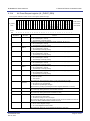
1
ASSP R-IN32M3 Series User’s Manual ・R-IN32M3-EC All information of mention is things at the time of this document publication, and Renesas Electronics may change the product or specifications that are listed in this document without a notice. Please confirm the latest information such as shown by website of Renesas Document number: R18UZ0003EJ0301 Issue date : Dec 25, 2014 Renesas Electronics www.renesas.com Notice 1. 2. 3. 4. 5. Descriptions of circuits, software and other related information in this document are provided only to illustrate the operation of semiconductor products and application examples. You are fully responsible for the incorporation of these circuits, software, and information in the design of your equipment. Renesas Electronics assumes no responsibility for any losses incurred by you or third parties arising from the use of these circuits, software, or information. Renesas Electronics has used reasonable care in preparing the information included in this document, but Renesas Electronics does not warrant that such information is error free. Renesas Electronics assumes no liability whatsoever for any damages incurred by you resulting from errors in or omissions from the information included herein. Renesas Electronics does not assume any liability for infringement of patents, copyrights, or other intellectual property rights of third parties by or arising from the use of Renesas Electronics products or technical information described in this document. No license, express, implied or otherwise, is granted hereby under any patents, copyrights or other intellectual property rights of Renesas Electronics or others. You should not alter, modify, copy, or otherwise misappropriate any Renesas Electronics product, whether in whole or in part. Renesas Electronics assumes no responsibility for any losses incurred by you or third parties arising from such alteration, modification, copy or otherwise misappropriation of Renesas Electronics product. Renesas Electronics products are classified according to the following two quality grades: "Standard" and "High Quality". The recommended applications for each Renesas Electronics product depends on the product's quality grade, as indicated below. "Standard": Computers; office equipment; communications equipment; test and measurement equipment; audio and visual equipment; home electronic appliances; machine tools; personal electronic equipment; and industrial robots etc. "High Quality": Transportation equipment (automobiles, trains, ships, etc.); traffic control systems; anti-disaster systems; anti-crime systems; and safety equipment etc. Renesas Electronics products are neither intended nor authorized for use in products or systems that may pose a direct threat to human life or bodily injury (artificial life support devices or systems, surgical implantations etc.), or may cause serious property damages (nuclear reactor control systems, military equipment etc.). You must check the quality grade of each Renesas Electronics product before using it in a particular application. You may not use any Renesas Electronics product for any application for which it is not intended. Renesas Electronics shall not be in any way liable for any damages or losses incurred by you or third parties arising from the use of any Renesas Electronics product for which the product is not intended by Renesas Electronics. 6. You should use the Renesas Electronics products described in this document within the range specified by Renesas Electronics, especially with respect to the maximum rating, operating supply voltage range, movement power voltage range, heat radiation characteristics, installation and other product characteristics. Renesas Electronics shall have no liability for malfunctions or damages arising out of the use of Renesas Electronics products beyond such specified ranges. 7. Although Renesas Electronics endeavors to improve the quality and reliability of its products, semiconductor products have specific characteristics such as the occurrence of failure at a certain rate and malfunctions under certain use conditions. Further, Renesas Electronics products are not subject to radiation resistance design. Please be sure to implement safety measures to guard them against the possibility of physical injury, and injury or damage caused by fire in the event of the failure of a Renesas Electronics product, such as safety design for hardware and software including but not limited to redundancy, fire control and malfunction prevention, appropriate treatment for aging degradation or any other appropriate measures. Because the evaluation of microcomputer software alone is very difficult, please evaluate the safety of the final products or systems manufactured by you. 8. Please contact a Renesas Electronics sales office for details as to environmental matters such as the environmental compatibility of each Renesas Electronics product. Please use Renesas Electronics products in compliance with all applicable laws and regulations that regulate the inclusion or use of controlled substances, including without limitation, the EU RoHS Directive. Renesas Electronics assumes no liability for damages or losses occurring as a result of your noncompliance with applicable laws and regulations. 9. Renesas Electronics products and technology may not be used for or incorporated into any products or systems whose manufacture, use, or sale is prohibited under any applicable domestic or foreign laws or regulations. You should not use Renesas Electronics products or technology described in this document for any purpose relating to military applications or use by the military, including but not limited to the development of weapons of mass destruction. When exporting the Renesas Electronics products or technology described in this document, you should comply with the applicable export control laws and regulations and follow the procedures required by such laws and regulations. 10. It is the responsibility of the buyer or distributor of Renesas Electronics products, who distributes, disposes of, or otherwise places the product with a third party, to notify such third party in advance of the contents and conditions set forth in this document, Renesas Electronics assumes no responsibility for any losses incurred by you or third parties as a result of unauthorized use of Renesas Electronics products. 11. This document may not be reproduced or duplicated in any form, in whole or in part, without prior written consent of Renesas Electronics. 12. Please contact a Renesas Electronics sales office if you have any questions regarding the information contained in this document or Renesas Electronics products, or if you have any other inquiries. (Note 1) "Renesas Electronics" as used in this document means Renesas Electronics Corporation and also includes its majority-owned subsidiaries. (Note 2) "Renesas Electronics product(s)" means any product developed or manufactured by or for Renesas Electronics. Instructions for the use of product In this section, the precautions are described for over whole of CMOS device. Please refer to this manual about individual precaution. When there is a mention unlike the text of this manual, a mention of the text takes first priority 1.Handling of Unused Pins Handle unused pins in accord with the directions given under Handling of Unused Pins in the manual. -The input pins of CMOS products are generally in the high-impedance state. In operation with an unused pin in the open-circuit state, extra electromagnetic noise is induced in the vicinity of LSI, associated shoot-through current flows internally, and malfunctions occur due to the false recognition of the pin state as an input signal become possible. Unused pins should be handled as described under Handling of Unused Pins in the manual. 2.Processing at Power-on The state of the product is undefined at the moment when power is supplied. -The states of internal circuits in the LSI are indeterminate and the states of register settings and pins are undefined at the moment when power is supplied. In a finished product where the reset signal is applied to the external reset pin, the states of pins are not guaranteed from the moment when power is supplied until the reset process is completed. In a similar way, the states of pins in a product that is reset by an on-chip power-on reset function are not guaranteed from the moment when power is supplied until the power reaches the level at which resetting has been specified. 3.Prohibition of Access to Reserved Addresses Access to reserved addresses is prohibited. -The reserved addresses are provided for the possible future expansion of functions. Do not access these addresses; the correct operation of LSI is not guaranteed if they are accessed. 4.Clock Signals After applying a reset, only release the reset line after the operating clock signal has become stable. When switching the clock signal during program execution, wait until the target clock signal has stabilized. -When the clock signal is generated with an external resonator (or from an external oscillator) during a reset, ensure that the reset line is only released after full stabilization of the clock signal. Moreover, when switching to a clock signal produced with an external resonator (or by an external oscillator) while program execution is in progress, wait until the target clock signal is stable. ・ARM, AMBA, ARM Cortex, Thumb and ARM Cortex-M3 are a trademark or a registered trademark of ARM Limited in EU and other countries. ・Ethernet is a registered trademark of Fuji Zerox Limited. ・IEEE is a registered trademark of the Institute of Electrical and Electronics Engineers, Inc. ・EtherCAT is a registered trademark of Beckhoff Automation GmbH, Germany. ・CC-Link and CC-Link IE Field are a registered trademark of CC-Link Partner Association (CLPA). ・Additionally all product names and service names in this document are a trademark or a registered trademark which belongs to the respective owners. ・Real-Time OS Accelerator and Hardware Real-Time OS is based on Hardware Real-Time OS of “ARTESSO” made in KERNELON SILICON Inc. How to use this manual 1. Purpose and target readers This manual is intended for users who wish to understand the functions of Industrial Ethernet network LSI “R-IN32M3-EC” (MC-10287F1-HN4-A) for designing application of it. It is assumed that the reader of this manual has general knowledge in the fields of electrical engineering, logic circuits, and microcontrollers. Particular attention should be paid to the precautionary notes when using the manual. These notes occur within the body of the text, at the end of each section, and in the Usage Notes section. The revision history summarizes the locations of revisions and additions. It does not list all revisions. Refer to the text of the manual for details. Literature Literature may be preliminary versions. Note, however, that the following descriptions do not indicate "Preliminary". Some documents on cores were created when they were planned or still under development. So, they may be directed to specific customers. Last four digits of document number(described as ****) indicate version information of each document. Please download the latest document from our web site and refer to it. The document related to R-IN32M3-EC Document name Document number R-IN32M3 series Datasheet R18DS0008EJ**** R-IN32M3-CL User’s Manual R18UZ0005EJ**** R-IN32M3 series User’s Manual Peripheral function R18UZ0007EJ**** R-IN32M3 Series Proguraming Manual (OS edition) R18UZ0011EJ**** R-IN32M3 Series Proguraming Manual (Driver edition) R18UZ0009EJ**** R-IN32M3-EC User’s Manual This manual 2. Notation of Numbers and Symbols Weight in data notation: Left is high-order column, right is low-order column Active low notation: xxxZ (capital letter Z after pin name or signal name) or xxx_N or xxnx (capital letter _N after pin name or signal name) (pin name or signal name contains small letter n) Note: explanation of (Note) in the text Caution: Item deserving extra attention Remark: Supplementary explanation to the text Numeric notation: Binary … xxxx , xxxxB or n’bxxxx (n bits) Decimal … xxxx Hexadecimal … xxxxH or n’hxxxx (n bits) Prefixes representing powers of 2 (address space, memory capacity): K (kilo)… 210 = 1024 M (mega)… 220 = 10242 G (giga)… 230 = 10243 Data Type: Word … 32 bits Halfword … 16 bits Byte … 8 bits Contents 1. 2. Overview ........................................................................................................................................................ 1 1.1 Introduction......................................................................................................................................................... 1 1.2 Overview ............................................................................................................................................................ 2 1.3 INTERNAL BLOCK DIAGRAM ...................................................................................................................... 4 1.4 Pin Placement (Top View) .................................................................................................................................. 5 Signals by function ........................................................................................................................................ 6 2.1 Signals by function ............................................................................................................................................. 6 2.1.1 Ethernet Signal........................................................................................................................................... 6 2.1.2 EtherCAT Slave Controller Signal ............................................................................................................ 8 2.1.3 External Memory Interface Signals ........................................................................................................... 9 2.1.4 External MPU Interface Signals .......................................................................................................... 11 2.1.5 Port Signals, Real-time port Signals ........................................................................................................ 12 2.1.6 Serial Flash ROM Interface Signals ........................................................................................................ 16 2.1.7 DMA Interface Signals ............................................................................................................................ 16 2.1.8 External Interrupt Input Signals ............................................................................................................... 17 2.1.9 Timer I/O Signals .................................................................................................................................... 18 2.1.10 Watchdog Timer Output Signals ............................................................................................................. 18 2.1.11 Trace Signals ........................................................................................................................................... 18 2.1.12 CPU Power Control Signals .................................................................................................................... 18 2.1.13 Serial Interface Signals ............................................................................................................................ 19 2.1.14 CC-Link Signals (Intelligent device station) ........................................................................................... 20 2.1.15 CC-Link Signals (Remote device station) ............................................................................................... 21 2.1.16 System Signals ......................................................................................................................................... 22 2.1.17 Test Signals .............................................................................................................................................. 23 2.1.18 Operation mode Setting Signals............................................................................................................... 24 2.2 Port status ......................................................................................................................................................... 25 2.3 Buffer Type and Recommended Connection of Unused Pins........................................................................... 26 2.3.1 Ethernet Signals ....................................................................................................................................... 26 2.3.2 External Memory/ MPU Interface Signals............................................................................................... 26 2.3.3 System Signals ......................................................................................................................................... 27 2.3.4 Test Signals .............................................................................................................................................. 27 2.3.5 Port Signals .............................................................................................................................................. 28 2.3.6 Operation Mode Setting Signals .............................................................................................................. 29 2.3.7 CC-Link Master Signal (Intelligent device station, Remote device station) ......................................... 29 Contents-1 2.3.8 Trace Signals ........................................................................................................................................... 29 3. Memory Maps .............................................................................................................................................. 30 4. Exception handling function......................................................................................................................... 34 4.1 Exceptions list ................................................................................................................................................... 34 4.2 Interrupt list ...................................................................................................................................................... 35 5. Peripheral function ....................................................................................................................................... 39 6. EtherCAT Slave Controller function ............................................................................................................ 40 6.1 Features ............................................................................................................................................................. 40 6.2 Peripheral circuit of EtherCAT ......................................................................................................................... 40 6.3 Interrupt list and I/O signals ............................................................................................................................. 41 6.4 Functional Overview......................................................................................................................................... 42 6.5 EtherCAT register list ....................................................................................................................................... 45 6.6 Peripheral Function Registers ........................................................................................................................... 50 6.6.1 EtherCAT PHY offset address setting register (CATOFFADD) ............................................................. 50 6.6.2 EtherCAT operation mode setting register (CATEMMD) ...................................................................... 51 6.6.3 EtherCAT reset register (CATRESET).................................................................................................... 52 6.7 ESC Information Register ................................................................................................................................. 53 6.7.1 Type register (TYPE)............................................................................................................................... 53 6.7.2 Revision register (REVISION) ................................................................................................................ 53 6.7.3 Build register (BUILD) ............................................................................................................................ 53 6.7.4 FMMUs supported register (FMMU_NUM) ........................................................................................... 54 6.7.5 SyncManagers supported register (SYNC_MANAGER) ........................................................................ 54 6.7.6 RAM Size register (RAM_SIZE) ............................................................................................................ 54 6.7.7 Port Descriptor register (PORT_DESC) .................................................................................................. 55 6.7.8 ESC Features supported register (FEATURE) ........................................................................................ 56 6.8 Station Address Registers ................................................................................................................................. 57 6.8.1 Configured Station Address register (STATION_ADR) ......................................................................... 57 6.8.2 Configured Station Alias register (STATION_ALIAS) .......................................................................... 57 6.9 Write Protection Registers ................................................................................................................................ 58 6.9.1 Write Register Enable register (WR_REG_ENABLE) ........................................................................... 58 6.9.2 Write Register Protection register (WR_REG_PROTECT) .................................................................... 58 6.9.3 ESC Write Enable register (ESC_WR_ENABLE) .................................................................................. 59 6.9.4 ESC Write Protection register (ESC_WR_PROTECT) ........................................................................... 59 6.10 6.10.1 Data Link Layer Registers ................................................................................................................................ 60 ESC Reset ECAT register (ESC_RESET_ECAT) .................................................................................. 60 Contents-2 6.10.2 ESC Reset PDI register (ESC_RESET_PDI) .......................................................................................... 61 6.10.3 ESC DL Control register (ESC_DL_CONTROL) ................................................................................... 62 6.10.4 Physical Read/Write Offset register (PHYSICAL_RW_OFFSET) ......................................................... 63 6.10.5 ESC DL Status register (ESC_DL_STATUS) ......................................................................................... 64 6.11 Application Layer Registers ............................................................................................................................. 66 6.11.1 AL Control register (AL_CONTROL) .................................................................................................... 66 6.11.2 AL Status register (AL_STATUS) .......................................................................................................... 67 6.11.3 AL Status Code register (AL_STATUS_CODE) .................................................................................... 67 6.11.4 RUN LED Override register (RUN_LED_OVERRIDE) ........................................................................ 68 6.11.5 ERR LED Override register (ERR_LED_OVERRIDE) .......................................................................... 69 6.12 PDI Registers .................................................................................................................................................... 70 6.12.1 PDI Control register (PDI_CONTROL) .................................................................................................. 70 6.12.2 ESC Configuration register (ESC_CONFIG) .......................................................................................... 71 6.12.3 PDI Configuration register (PDI_CONFIG) ............................................................................................ 72 6.12.4 SYNC/LATCH PDI Configuration register (SYNC_LATCH_CONFIG) .............................................. 73 6.12.5 Extended PDI Configuration register (EXT_PDI_CONFIG) .................................................................. 74 6.13 Interrupts Registers ........................................................................................................................................... 75 6.13.1 ECAT Event Mask register (ECAT_EVENT_MASK) ........................................................................... 75 6.13.2 AL Event Mask register (AL_EVENT_MASK)...................................................................................... 75 6.13.3 ECAT Event Request register (ECAT_EVENT_REQ) ........................................................................... 76 6.13.4 AL Event Request register (AL_EVENT_REQ) ..................................................................................... 77 6.14 Error Counters Registers ................................................................................................................................... 78 6.14.1 Rx Error Counter n register (RX_ERR_COUNTn) ................................................................................. 78 6.14.2 Forwarded Rx Error counter n register (FWD_RX_ERR_COUNTn) ..................................................... 79 6.14.3 ECAT Processing Unit Error Counter register (ECAT_PROC_ERR_COUNT) ..................................... 79 6.14.4 PDI Error Counter register (PDI_ERR_COUNT) ................................................................................... 80 6.14.5 Lost Link Counter n register (LOST_LINK_COUNTn) ......................................................................... 80 6.15 Watchdogs Registers......................................................................................................................................... 81 6.15.1 Watchdog Divider register (WD_DIVIDE) ............................................................................................. 81 6.15.2 Watchdog Time PDI register (WDT_PDI) .............................................................................................. 81 6.15.3 Watchdog Time Process Data register (WDT_DATA) ........................................................................... 82 6.15.4 Watchdog Status Process Data register (WDS_DATA) .......................................................................... 82 6.15.5 Watchdog Counter Process Data register (WDC_DATA) ....................................................................... 83 6.15.6 Watchdog Counter PDI register (WDC_PDI).......................................................................................... 83 6.16 SII EEPROM Interface Registers ..................................................................................................................... 84 6.16.1 EEPROM Configuration register (EEP_CONF) ...................................................................................... 84 6.16.2 EEPROM PDI Access State register (EEP_STATE)............................................................................... 84 6.16.3 EEPROM Control/Status register (EEP_CONT_STAT) ......................................................................... 85 6.16.4 EEPROM Address register (EEP_ADR) ................................................................................................. 86 Contents-3 6.16.5 6.17 EEPROM Data register (EEP_DATA) .................................................................................................... 87 MII Management Interface Registers ............................................................................................................... 88 6.17.1 MII Management Control/Status register (MII_CONT_STAT) .............................................................. 88 6.17.2 PHY Address register (PHY_ADR) ........................................................................................................ 89 6.17.3 PHY Register Address register (PHY_REG_ADR) ................................................................................ 89 6.17.4 PHY Data register (PHY_DATA) ........................................................................................................... 90 6.17.5 MII Management ECAT Access State register (MII_ECAT_ACS_STAT) ............................................ 90 6.17.6 MII Management PDI Access State register (MII_PDI_ACS_STAT) .................................................... 91 6.17.7 PHY Port Status n register (PHY_STATUSn)......................................................................................... 92 6.18 FMMU Registers .............................................................................................................................................. 93 6.18.1 FMMU Logical Start Address m register (FMMUm.L_START_ADR) ................................................. 93 6.18.2 FMMU Length m register (FMMUm.LEN) ............................................................................................ 93 6.18.3 FMMU Logical Start bit m register (FMMUm.L_START_BIT) ............................................................ 94 6.18.4 FMMU Logical Stop bit m register (FMMUm.L_STOP_BIT) ............................................................... 94 6.18.5 FMMU Physical Start Address m register (FMMUm.P_START_ADR) ................................................ 95 6.18.6 FMMU Physical Start bit m register (FMMUm.P_START_BIT) ........................................................... 95 6.18.7 FMMU Type m register (FMMUm.TYPE) ............................................................................................. 96 6.18.8 FMMU Activate m register (FMMUm.ACT) .......................................................................................... 96 6.19 SyncManager Registers .................................................................................................................................... 97 6.19.1 SyncManager Physical Start Address m register (SMm.P_START_ADR) ............................................. 97 6.19.2 SyncManager Length m register (SMm.LEN) ......................................................................................... 97 6.19.3 SyncManager Control m register (SMm.CONTROL) ............................................................................. 98 6.19.4 SyncManager Status m register (SMm.STATUS) ................................................................................... 99 6.19.5 SyncManager Activate m register (SMm.ACT) .................................................................................... 100 6.19.6 SyncManager PDI Control m register (SMm.PDI_CONT) ................................................................... 101 6.20 Distributed Clocks Registers........................................................................................................................... 102 6.20.1 DC Receive Times Registers ................................................................................................................. 102 6.20.2 DC Time Loop Control Unit Registers .................................................................................................. 103 6.20.3 Cyclic Unit Control Registers ................................................................................................................ 108 6.20.4 SYNC Out Unit Registers ...................................................................................................................... 109 6.20.5 Latch In Unit Registers .......................................................................................................................... 114 6.20.6 SyncManager Event Times Registers .................................................................................................... 121 6.21 ETC Registers ................................................................................................................................................. 123 6.21.1 PRODUCT ID register (PRODUCT_ID) .............................................................................................. 123 6.21.2 Vender ID register (VENDOR_ID) ....................................................................................................... 123 6.21.3 User RAM (USER_RAM) ..................................................................................................................... 124 6.21.4 Process Data RAM (DATA_RAM) ....................................................................................................... 125 Contents-4 7. Etherne PHY Function ............................................................................................................................... 126 7.1 Features ........................................................................................................................................................... 126 7.2 Special functions ............................................................................................................................................. 126 7.2.1 Low latency function ............................................................................................................................. 126 7.2.2 Quick auto-negotiation function ............................................................................................................ 127 7.2.3 Cable diagnostic function (TDR function)............................................................................................. 129 7.2.4 Fast link-loss detection function ............................................................................................................ 132 7.3 power down mode........................................................................................................................................... 133 7.3.1 Hardware power down mode ................................................................................................................. 133 7.3.2 Software power down mode .................................................................................................................. 133 7.3.3 Energy detection power down mode...................................................................................................... 133 7.4 MII management register with Ethernet PHY internal ................................................................................... 134 7.4.1 Register 0 - Control Register ................................................................................................................. 135 7.4.2 Register 1 – Status Register ................................................................................................................... 136 7.4.3 Register 2, 3 - PHY Identifier ................................................................................................................ 137 7.4.4 Register 4 - Auto-Negotiation Advertisement Register ......................................................................... 138 7.4.5 Register 5 - Auto-Negotiation Link Partner Ability (Base Page) Register ............................................ 139 7.4.6 Register 5 – Auto-Negotiation Link Partner Ability (Next Page) Register ........................................... 140 7.4.7 Register 6- Auto-Negotiation Expansion Register ................................................................................. 141 7.4.8 Register 7 - Auto-Negotiation Next Page Transmit Register ................................................................. 142 7.4.9 Register 16- Silicon Revision Register .................................................................................................. 143 7.4.10 Register 17- mode control/status Register ............................................................................................. 144 7.4.11 Register 18- Special mode register ........................................................................................................ 146 7.4.12 Register 19-Reserved ............................................................................................................................. 147 7.4.13 Register 20 – Reserved .......................................................................................................................... 147 7.4.14 Register 21 – Reserved .......................................................................................................................... 148 7.4.15 Register 22 – Reserved .......................................................................................................................... 148 7.4.16 Register 23-BER counter Register ......................................................................................................... 149 7.4.17 Register 24-FEQ monitor Register ........................................................................................................ 150 7.4.18 Register 25-Diagnostic control/Status Register ..................................................................................... 151 7.4.19 Register 26-Diagnostic counter register ................................................................................................. 152 7.4.20 Register 27-Special control/Status instruction register .......................................................................... 153 7.4.21 Register 28 – Reserved .......................................................................................................................... 154 7.4.22 Register 29- Interrupt Factor Register ................................................................................................... 155 7.4.23 Register 30-Interrupt Factor Mask Register........................................................................................... 156 7.4.24 Register 31- PHY special control/Status register ................................................................................... 157 7.5 7.5.1 Ethernet PHY function setting register ........................................................................................................... 158 List of registers ...................................................................................................................................... 158 Contents-5 8. 7.5.2 Ethernet PHY operation mode control register (PHYMD) .................................................................... 159 7.5.3 Ethernet PHY power-up status register (PHYPUS) ............................................................................... 160 Port function .............................................................................................................................................. 161 8.1 Features ........................................................................................................................................................... 161 8.2 Port configuration ........................................................................................................................................... 162 8.3 Registers ......................................................................................................................................................... 164 8.3.1 Port registers (P, RP) ............................................................................................................................. 170 8.3.2 Port mode registers (PM, RPM)............................................................................................................. 173 8.3.3 Port mode control register (PMC, RPMC)............................................................................................. 176 8.3.4 Port function control registers (PFC, RPFC) ......................................................................................... 179 8.3.5 Port function control expansion registers (PFCE, RPFCE) ................................................................... 182 8.3.6 Port pin input registers (PIN, RPIN) ...................................................................................................... 185 8.4 Available combinations of alternate functions ................................................................................................ 188 8.5 Buffer function change registers (DRCTLP) .................................................................................................. 192 8.5.1 Port 1 buffer function change registers (DRCTLP1L, DRCTLP1H) ..................................................... 193 8.5.2 Port 3 buffer function change registers (DRCTLP3L, DRCTLP3H) ..................................................... 194 8.5.3 Port 4 buffer function change registers (DRCTLP4L, DRCTLP4H) ..................................................... 195 8.5.4 Port 5 buffer function change registers (DRCTLP5L, DRCTLP5H) <R>............................................. 196 8.5.5 Real-time port 0 buffer function change registers (DRCTLRP0L, DRCTLRP0H) ............................... 197 8.5.6 Real-time port 1 buffer function change registers (DRCTLRP1L, DRCTLRP1H) ............................... 198 8.5.7 Real-time port 2 buffer function change registers (DRCTLRP2L, DRCTLRP2H) ............................... 199 8.5.8 Real-time port 3 buffer function change registers (DRCTLRP3L, DRCTLRP3H) ............................... 200 8.6 8.6.1 Reading and writing via I/O ports .......................................................................................................... 201 8.6.2 Alternate function pin output status in control mode ............................................................................. 201 8.7 9. Operation of port functions ............................................................................................................................. 201 Trigger-synchronous ports (RP00 to RP37).................................................................................................... 202 Electrical Specifications ............................................................................................................................. 203 Contents-6 Contents of figures Figure 3.1 Memory map (ALL)............................................................................................................................ 30 Figure 3.2 Memory map (APB Peripheral registers area) .................................................................................... 31 Figure 3.3 Memory map (External memory area) ................................................................................................ 32 Figure 3.4 Memory map (CC-Link Master area).................................................................................................. 32 Figure 3.5 External MPU interface area ............................................................................................................... 33 Figure 6.1 Peripheral circuit of EtherCAT ........................................................................................................... 40 Figure 7.1 Preamble of Ethernet frames ............................................................................................................. 126 Figure 7.2 Behavior of cable disconnected ........................................................................................................ 129 Figure 7.3 Behavior of cable short-circuited ...................................................................................................... 129 Figure 7.4 cable diagnostic process flow............................................................................................................ 131 Figure 8.1 Basic port circuit configuration ......................................................................................................... 163 Figure 8.2 Port registers (in 8-bit notation) ........................................................................................................ 170 Figure 8.3 Port registers (in 16-bit notation) ...................................................................................................... 171 Figure 8.4 Port registers (in 32-bit notation) ...................................................................................................... 172 Figure 8.5 Port mode registers (in 8-bit notation) .............................................................................................. 173 Figure 8.6 Port mode registers (in 16-bit notation) ............................................................................................ 174 Figure 8.7 Port mode registers (in 32-bit notation) ............................................................................................ 175 Figure 8.8 Port mode control registers (in 8-bit notation) .................................................................................. 176 Figure 8.9 Port mode control registers (in 16-bit notation) ................................................................................ 177 Figure 8.10 Port mode control registers (in 32-bit notation) ................................................................................ 178 Figure 8.11 Port function control registers (in 8-bit notation).............................................................................. 179 Figure 8.12 Port function control registers (in 16-bit notation)............................................................................ 180 Figure 8.13 Port function control registers (in 32-bit notation)............................................................................ 181 Figure 8.14 Port function control expansion registers (in 8-bit notation) ............................................................ 182 Figure 8.15 Port function control expansion registers (in 16-bit notation) .......................................................... 183 Figure 8.16 Port function control expansion registers (in 32-bit notation) .......................................................... 184 Figure 8.17 Port pin input registers (in 8-bit notation) ......................................................................................... 185 Figure 8.18 Port pin input registers (in 16-bit notation) ....................................................................................... 186 Figure 8.19 Configuration of Trigger-Synchronous Ports.................................................................................... 202 Contents-7 Contents of tables Table4.1 Interrupt list ............................................................................................................................................. 35 Table 6.1 Features of EtherCAT Slave Controller .................................................................................................. 40 Table 6.2 Interrupt list of EtherCAT Slave Controller ............................................................................................ 41 Table 6.3 I/O signals of EtherCAT Slave Controller (excluding PHY MDI signals) ............................................. 41 Table 6.4 Typical functions of EtherCAT Slave Controller and supported function by R-IN32M3-EC ................ 42 Table 7.1 Summary of PHY MII Management registers ...................................................................................... 134 Contents-8 R18UZ0003EJ0301 R-IN32M3-EC User’s Manual 1. Overview 1.1 Introduction Dec 25, 2014 Ethernet communication continues to spread rapidly in the field of industrial automation as manufacturers seek to improve the capability, efficiency, and flexibility of their organizations. Modern Industrial Ethernet applications require high-speed real-time response, low power consumption, and high performance. These requirements are not necessarily met by traditional methods such as hard-wired Ethernet processors or dedicated high-speed CPUs. Renesas' R-IN32M3-EC of large-scale integrated circuits (LSI) are specifically tailored to meet the demands of Industrial Ethernet applications. Key features include: • • • • • • • • High-speed, real-time, deterministic, low-latency, low-jitter response for real-time applications Low power consumption Integrated ARM Cortex-M3 core for flexibility Integrated Real-Time OS Accelerator with support for μITRON version 4.0 Integrated 10/100Mbps EtherPHY Dedicated, DMA controller and buffer for the network processor High performance with low CPU usage by offloading functions to Real-Time OS Accelerator Multiple timers, serial interfaces, general purpose I/O (GPIO), external memory interfaces R-IN32M3-EC User’s Manual 1.2 1. Overview Overview Table 1.1 Overview of R-IN32M3-EC(1/2) Product R-IN32M3-EC Item CPU core ARM Cortex-M3 32-bit RISC CPU + Real-Time OS Accelerator (Hardware Real-Time OS, HW-RTOS) Operating frequency 100MHz Instruction set ThumbⓇ-2 instruction ARMv7-M architecture Instruction RAM 768KByte (RAM w/ECC) Data RAM 512KByte (RAM w/ECC) Buffer RAM 64KByte (RAM w/ECC) Internal System Bus - 32-bit system bus at 100MHz - 128-bit communication bus at 100MHz DMA Bus - 4 channels + 1 channel (for Real-time port) (System Bus Side) - Supports software and various interrupt-triggered DMA Boot options - Serial Flash ROM Boot - External Memory Boot - External MPU Boot External Memory Support - 16-bit or 32-bit bus interface - Page ROM / ROM / SRAM interface - Synchronous burst memory interface - Four chip selects for external SRAM - 256MByte (max) external memory space - Programmable wait function External MPU interface - 16-bit or 32-bit bus interface - General-purpose interface for static memory - Address space:2MByte (Instruction RAM, Data RAM, Register area) Serial Flash ROM Memory Controller - Support serial interface compatible with SPI of the companies - Support direct boot from serial memory device - Support Fast Read, Fast Read Dual Output, Fast Read Dual I/O mode - Direct layout in memory space Interrupt Support - 29 external interrupt ports Internal Peripherals I/O Ports CMOS I/O:96ports(max) System Timers - Internal timer of Hardware RTOS - internal timer of CPU - 4channel timer array - 32bit counter & 32bit data register - counter by external signal R18UZ0003EJ0301 Dec 25, 2014 Page 2 of 203 R-IN32M3-EC User’s Manual Table 1.1 1. Overview Overview of R-IN32M3-EC(2/2) Product R-IN32M3-EC Item Internal Peripherals (cont.) Watchdog Timer - 1 channel - Software-triggered start mode - Watchdog error response options: - Generate Non-Maskable Interrupt (NMI) - Generate Reset Asynchronous serial interface - 2 channels - Full duplex - FIFOs: 10-bit x 16 receive and 8-bit x 16 transmit - Support output of receive errors and status - Character length: 7 or 8-bit - Parity bit options: odd, even, 0- , none - Transmit stop bits: 1 or 2-bit I2C Serial interface - 2 channels - Operation modes: normal or high-speed - Transfer modes: single-transfer mode, or continuous-transfer mode - Transmission data length: 8-bit CAN controller - 2 channels - Conforming to ISO11898 - Support to transfer and receive normal frame and expand frame - Transmission speed: 1Mbps (max) Clock Synchronized Serial - 2 channels Interface - Synchronized Serial data transmission by three-wire system - Selectable Master mode or Slave mode - Built-in Baud-rate generator - Transmission data length: 7bit - 16bit CC-Link - Intelligent device station Note3 <R> - Remote device station 10/100Mbps EtherPHY Note2 - 2ports - Support for 10BaseT and 100BaseTX/FX EtherCAT EtherCAT Slave controller On-chip debug function - Select serial wire or JTAG - Support Full Trace (Built-in ETM) Internal PLL Generates various clocks from 25MHz input clock Power supply voltage I/O:VDD33 = 3.3±0.3V Internal circuit :VDD10 = 1.0±0.1V Note. Please ask us about a detail for support. R18UZ0003EJ0301 Dec 25, 2014 Page 3 of 203 R18UZ0003EJ0301 Dec 25, 2014 S DMAC _RTPORT M HOST_CPU S DMAC M DMAC_RTPORT DMAC CPU I-Code CPU D-Code CPU System S S MUX S Serial Flash ROM MEMC S S M M M NVIC Debug GPIO S S MUX S S S MUX S Real-Time GPIO S Hardware Real-Time OS Bridge OS S Hardware Function Control Buffer RAM 64KB(ECC) S S MEMC S S MUX S Selector S MUX S S Data RAM 512KB(ECC) S Buffer Allocator S S S S MUX S M MAC_DMA M Ext_ Micon Interface S S S APB Gigabit Ether Buffer ID S Ether SWITCH AHB_APB Bridge S S MUX MUX S S EtherCAT MAC_TOP INT_DMA M Instruction RAM 768KB(ECC) S MUX S S AHB2DMA M 128bit Communication Bus Header Endec M M 128bit Hardware Function Bus S S MUX CC-Link Bridge S S HOST_CPU DMAC_RTPORT DMAC CPU I-Code CPU D-Code CPU System PHY PHY 1.3 Cortex-M3 CPU R-IN32M3-EC R-IN32M3-EC User’s Manual 1. Overview INTERNAL BLOCK DIAGRAM Timer Array UART × 2ch I2C × 2ch CAN × 2ch CSI × 2ch WDT Page 4 of 203 R18UZ0003EJ0301 Dec 25, 2014 P0_ SD_P D13 RP23 RP25 P0_ RD_N P0_ SD_N 14 13 12 RP16 RP17 RP10 RP12 RP14 RP15 B RP37 RP11 RP13 GND A 4 3 2 1 C RP03 RP05 VDD15 RP35 RP36 5 D RP00 RP01 RP02 RP04 GND E P74 P75 P76 P77 VDD33 GND RP06 RP07 RP33 RP34 6 GND RP31 RP32 P0_FX_ TEST EN_OUT DOUT5 GND VDD33 GND TMC1 GND D8 A16 A9 A8 7 RP30 RP26 RP22 D15 VDD15 D9 D7 A13 A12 RP20 VDD33 VDDQ_ PECL_B0 RP27 D14 D11 D10 A20 A19 A7 A6 E P0_TD_ P0_TD_ OUT_N OUT_P GND RP21 D12 D5 D3 A11 A10 D 8 9 10 VDD15 P0_ RD_P D6 15 11 RP24 D4 16 A18 A17 C F TEST3 P70 P71 P72 GND GND VDD33 GND VDD33 GND GND VDD33 GND A15 A5 A4 A3 A2 F H G H BGND AGND_ REG AVDD_ REG FB TEST2 P60 VDD33 GND VDD10 GND GND GND GND VDD10 GND P43 CSZ0 GND AGND P61 P73 GND VDD33 GND VDD10 VDD10 VDD10 VDD10 GND VDD33 A14 WRZ1 WRZ0 WRSTBZ P0VDD BUSCLK ARXTX G J LX GND TEST1 P62 VDD33 GND VDD10 GND GND GND GND VDD10 VDD33 P40 RDZ K BVDD GND GND P63 P65 GND VDD10 GND GND GND GND VDD10 GND P44 P41 L VDD15 P67 P66 P64 TCK GND VDD10 GND GND GND GND VDD10 GND P47 P42 AGND VDD33 ESD VDD15 VSSA PLLCB P0_ TX_P L VDD APLL P0_ RX_P K P0_ TX_N J P0_ RX_N M N P46 AGND P1_ TX_P P1_ TX_N P M P07 P05 P06 P00 TRSTZ VDD33 GND VDD10 VDD10 VDD10 VDD10 GND VDD33 N P04 P03 P01 P20 GND GND VDD33 GND GND VDD33 GND VDD33 GND R P P02 P22 P23 P21 R P24 P25 P26 P27 VDD15 GND PLL_ GND TDO P10 P17 GND VDD33 HWRZ SEL PLL_ VDD TMS TDI GND MEMC SEL HIF SYNC ADMUX MODE T XT1 GND P36 P34 OSCTH P15 P16 VDD33 P1_ SD_N P1_ RD_N VDD33 CCM_ CLK80M BOOT1 RESETZ TRACE DATA0 TRACE CLK P53 GND V U XT2 P37 P33 P30 P13 P14 V GND P35 P32 P31 P12 P1_FX_ EN_OUT P1_TD_ P1_TD_ OUT_P OUT_N GND P1_ SD_P VDDQ_ PECL_B1 P11 P1_ RD_P GND BOOT 0 MEM IFSEL VDD15 GND VDD15 PONRZ BUS32 EN TMC2 TRACE DATA2 TRACE DATA1 RST OUTZ P54 P55 P56 U P52 P51 P50 T JTAG SEL NMIZ GND AGND P1VDD ARXTX TRACE DATA3 P57 VDD15 P1_ RX_P P1_ RX_N TMODE TMODE TMODE 2 1 0 P45 ATP EXT RES VDD ACB 1 2 3 4 5 6 7 8 9 10 11 12 13 14 15 16 17 18 1.4 D1 D2 17 D0 B GND A 18 R-IN32M3-EC User’s Manual 1. Overview Pin Placement (Top View) Page 5 of 203 R-IN32M3-EC User’s Manual 2. Signals by function 2. Signals by function 2.1 Signals by function 2.1.1 (1) Ethernet Signal Media Interface Pin Name I/O Function Active Level during reset & Level after reset P0_RX_P I PHY0 Receive data (+) - - P0_RX_N I PHY0 Receive data (-) - - P1_RX_P I PHY1 Receive data (+) - - P1_RX_N I PHY1 Receive data (-) - - P0_TX_P O PHY0 Transmit data (+) - - P0_TX_N O PHY0 Transmit data (-) - - P1_TX_P O PHY1 Transmit data (+) - - P1_TX_N O PHY1 Transmit data (-) - - P0_SD_P I PHY0 100BASE-FX Signal Detect (+) High - P0_SD_N I PHY0 100BASE-FX Signal Detect (-) Low - P1_SD_P I PHY1 100BASE-FX Signal Detect (+) High - P1_SD_N I PHY1 100BASE-FX Signal Detect (-) Low - P0_RD_P I PHY0 100BASE-FX Receive data (+) - - P0_RD_N I PHY0 100BASE-FX Receive data (-) - - P1_RD_P I PHY1 100BASE-FX Receive data (+) - - P1_RD_N I PHY1 100BASE-FX Receive data (-) - - P0_TD_OUT_P O PHY0 100BASE-FX Transmit data (+) - - P0_TD_OUT_N O PHY0 100BASE-FX Transmit data (-) - - P1_TD_OUT_P O PHY1 100BASE-FX Transmit data (+) - - P1_TD_OUT_N O PHY1 100BASE-FX Transmit data (-) - - P0_FX_EN_OUT O PHY0 100BASE-FX FX Enable Indication High - High - 1:100BASE-FX mode P1_FX_EN_OUT O PHY1 100BASE-FX FX Enable Indication 1:100BASE-FX mode Remark In MDI-X mode, the input and output attributes of TXP/TXN and RXP/RXN are reversed. R18UZ0003EJ0301 Dec 25, 2014 Page 6 of 203 R-IN32M3-EC User’s Manual (2) 2. Signals by function Other Signals Pin Name I/O Function Shared Active Port Level during reset & Level after reset P0LINKLEDZ O SIP_PHY0 Link status LED port P06 Low P1LINKLEDZ O SIP_PHY1 Link status LED port P07 Low ETHSWSECOUT O EtherSwitch Event par 1sec output port P24 High Hi-Z P0DUPLEXLEDZ O SIP_PHY0 half-duplex status LED port P70 - With internal pull-up Note2 Hi-Z resistor 0 : full-duplex 1 : half-duplex P0SPEED100LEDZ O Note2 SIP_PHY0 100-BASE status LED port Note2 P0SPEED10LEDZ O SIP_PHY0 10-BASE status LED port P1DUPLEXLEDZ O SIP_PHY1 half-duplex status LED port P72 Low P73 Low P74 - P76 Low Note2 0 : full-duplex 1 : half-duplex P1SPEED100LEDZ O SIP_PHY1 100-BASE status LED port Note2 Note2 P1SPEED10LEDZ O SIP_PHY1 10-BASE status LED port P77 Low P0ACTLEDZ O SIP_PHY0 RX status LED port Note2 RP02 Low SIP_PHY1 TX status LED port Note2 RP04 Low P1ACTLEDZ R18UZ0003EJ0301 Dec 25, 2014 O Page 7 of 203 R-IN32M3-EC User’s Manual 2.1.2 2. Signals by function EtherCAT Slave Controller Signal Pin Name I/O Function Shared Active Port Level during reset & Level after reset CATLEDRUN O Ether CAT RUN LED port P00 High CATIRQ O Ether CAT IRQ port P01 High CATLEDSTER O Ether CAT Dual-color State LED port P02 High CATLEDERR O Ether CAT Error LED port P03 High CATLINKACT0, O Ether CAT Link / Activity LED port P04-P05 High O Ether CAT SYNC1 port P10 High Hi-Z CATLINKACT1 CATSYNC1 Hi-Z With internal pull-up resistor CATSYNC0 O Ether CAT SYNC0 port P11 High Hi-Z With internal pull-down resistor CATLATCH1 I Ether CAT LATCH1 port P10 High Hi-Z With internal pull-up resistor CATLATCH0 I Ether CAT LATCH0 port P11 High Hi-Z With internal pull-down resistor CATI2CCLK O Ether CAT EEPROM I2C clock port P22 - CATI2CDATA I/O Ether CAT EEPROM I2C data port P23 - CATRESTOUT O Ether CAT PHY RESETOUT port P56 - Hi-Z Hi-Z With internal pull-up resistor R18UZ0003EJ0301 Dec 25, 2014 Page 8 of 203 R-IN32M3-EC User’s Manual 2.1.3 2. Signals by function External Memory Interface Signals Pin Name I/O Function Shared Shared Signal port Active Level during Level after reset reset BUSCLK O Bus clock output port - - - - - CSZ0 O Chip select signal output HCSZ - Low Hi-Z High CSZ1 O port HPGCSZ P44 With Hi-Z CSZ2 O - P51 internal With CSZ3 O - P50 pull-up internal resistor pull-up resistor A1 O Address output port HA1 P40 - Hi-Z Low With internal pull-up resistor A2-A20 O HA2-HA20 - Hi-Z A21-A27 O - RP21- With Hi-Z RP27 internal With - pull-down internal resistor pull-down D0-D15 Note1 I/O Data bus port HD0-HD15 resistor D16-D31 Note1 I/O HD16-HD3 RP30- - Hi-Z 1 RP37 With internal pull-up RP10- resistor RP17 RDZ O Read strobe output port HRDZ - Low Hi-Z WRSTBZ O Write strobe output port HWRSTBZ - Low With WRZ0, WRZ1/ O Effectively Byte lane strobe HWRZ0, - Low internal output port HWRZ1/ pull-up HBENZ0, resistor BENZ0, BENZ1 High HBENZ1 WRZ2, WRZ3/ O BENZ2, BENZ3 HWRZ2, RP06, HWRZ3/ RP07 HBENZ2, HBENZ3 WAITZ I Wait signal input port WAITZ1-WAITZ3 HWAITZ P41 - P45-P With internal pull-up 47 resistor Note2 BCYSTZ / ADVZ O Address valid output port Note3 HBCYSTZ RP20 Low Low Hi-Z Hi-Z With internal pull-up resistor Remark External Memory Interface Signal expects BUSCLK is an input signal while the internal reset signal (HRESETZ) is active. R18UZ0003EJ0301 Dec 25, 2014 Page 9 of 203 R-IN32M3-EC User’s Manual 2. Signals by function Note1. When using synchronous burst access MEMC this port is shared with Address port when ADMUXMODE is high. Note2. This port is available only when using synchronous burst access MEMC. Note3. This port functions as BCYSTZ when using asynchronous SRAM MEMC, it functions as ADVZ when using synchronous burst access MEMC R18UZ0003EJ0301 Dec 25, 2014 Page 10 of 203 R-IN32M3-EC User’s Manual 2.1.4 2. Signals by function External MPU Interface Signals Pin Name HBUSCLK I/O I Function Bus clock for Host MPU Shared Signal INTPZ11 Shared Active port P43 - output port Level during reset & Level after reset Hi-Z With internal pull-up HCSZ I Chip select signal input port CSZ0 - Low HPGCSZ I Pogrom mode Chip select CSZ1 P44 Low HWAITZ O Wait signal output port WAITZ P41 Low HA1 I Address input port A1 P40 - resistor signal input port Hi-Z With internal pull-up resistor HA2-HA20 I HD0-HD15 I/O HD16-HD31 I/O Data bus port A2-A20 - D0-D15 - Hi-Z D16-D31 RP30- Hi-Z RP37 With internal pull-up RP10- resistor - With internal pull-down resistor RP17 HRDZ I Read strobe input port RDZ - Low Hi-Z HWRSTBZ I Write strobe output port WRSTBZ - Low With internal pull-up HWRZ0, HWRZ1/ I Effectively Byte lane strobe WRZ0, WRZ1/ - Low resistor input port BENZ0, BENZ1 High HBENZ0,HBENZ1 HWRZ2, HWRZ3/ I HBENZ2,HBENZ3 WRZ2, WRZ3/ RP06, BENZ2, BENZ3 RP07 HERROUTZ O Error interrupt output port SLEEPING P42 Low HBCYSTZ I Bus cycle input port BCYSTZ / ADVZ RP20 Low Hi-Z With internal pull-up resistor Caution When you use asynchronous mode, please input Low into a HBUSCLK pin.. Remark External MPU interface signals operate as an External MPU interface durinug reset. R18UZ0003EJ0301 Dec 25, 2014 Page 11 of 203 R-IN32M3-EC User’s Manual 2.1.5 2. Signals by function Port Signals, Real-time port Signals Port Signals and Real-time port Signals are configured as 12 sets of 8-bit ports. They are able to realize 32-bit access by grouping 4 ports; i.e. Ports 0-3, Ports 4-7 or Real-time ports 0-3. (1/4) Port Mode 1 Name P0 P1 Mode 2 Mode 3 Mode 4 P00 INTPZ0 CATLEDRUN - - P01 INTPZ1 CATIRQ - - P02 INTPZ2 CATLEDSTER - - P03 INTPZ3 CATLEDERR - CCS_MON5 P04 INTPZ4 CATLINKACT0 - CCS_MON6 P05 INTPZ5 CATLINKACT1 - CCS_MON7 P06 - P0LINKLEDZ - CCS_MON0 P07 - P1LINKLEDZ - CCS_RESOUT P10 CATLATCH1 CATSYNC1 - CCS_REFSTB Level during reset & Level after reset Hi-Z Hi-Z With internal pull-up resistor P11 CATLATCH0 CATSYNC0 - CCS_MON4 Hi-Z With internal pull-down resistor P12 INTPZ6 - - - Hi-Z P13 INTPZ7 - CCS_WDTZ / - With internal pull-up P14 SMSCK - - - P15 SMSI - - - P16 SMSO - - - P17 SMCSZ - - - P20 RXD0 - CCM_LINKERRZ - P21 TXD0 - CCM_ERRZ - P22 INTPZ8 CATI2CCLK CCS_IOTENSU - P23 INTPZ9 CATI2CDATA CCS_SENYU0 - P24 INTPZ10 ETHSWSECOUT CCS_SENYU1 - P25 WDTOUTZ - CCS_ERRZ - P26 TIN1 TOUT1 CCM_RUNZ / - resistor CCM_WDTENZ P2 Hi-Z CCS_RUNZ P27 TIN0 R18UZ0003EJ0301 Dec 25, 2014 TOUT0 - - Page 12 of 203 R-IN32M3-EC User’s Manual 2. Signals by function (2/4) Port Mode 1 Name P3 P4 P5 Mode 2 Mode 3 Mode 4 Level during reset & Level after reset P30 RXD1 - - - Hi-Z P31 TXD1 - - - With internal pull-up P32 DMAREQZ1 - - CCS_MON1 resistor P33 DMAACKZ1 - - CCS_MON2 P34 DMATCZ1 - - CCS_MON3 P35 CSISCK1 INTPZ22 CCM_IRLZ - P36 CSISI1 INTPZ23 CCS_FUSEZ - P37 CSISO1 INTPZ24 CCM_MSTZ - P40 A1 HA1 - - Hi-Z P41 WAITZ HWAITZ - - With internal pull-up P42 SLEEPING HERROUTZ CCM_SDGCZ - resistor P43 INTPZ11 HBUSCLK - - P44 CSZ1 HPGCSZ - - P45 CSISCK0 WAITZ1 - - P46 CSISI0 WAITZ2 - - P47 CSISO0 WAITZ3 - - P50 CSZ3 - CCM_LNKRUNZ / - CCS_LNKRUNZ P51 CSZ2 - CCM_RDLEDZ / - CCS_RDLEDZ P52 TIN3 TOUT3 CCS_SDGATEON - Hi-Z With internal pull-down resistor P53 CRXD0 CCS_RD CCM_RD - Hi-Z P54 CTXD0 CCS_SD CCM_SD - With internal pull-up P55 CRXD1 - - - resistor P56 CTXD1 CATRESTOUT - - P57 TIN2 TOUT2 - - R18UZ0003EJ0301 Dec 25, 2014 Page 13 of 203 R-IN32M3-EC User’s Manual 2. Signals by function (3/4) Port Mode 1 Name P6 P7 Mode 2 Mode 3 Mode 4 P60 SCL0 - - - P61 SDA0 - - - P62 RTDMAREQZ - CCM_MDIN0 - P63 RTDMAACKZ - CCM_MDIN1 - P64 RTDMATCZ - CCM_MDIN2 - P65 DMAREQZ0 - CCM_MDIN3 - P66 DMAACKZ0 - - - P67 DMATCZ0 - - - P70 CSICS00 P0DUPLEXLEDZ CCS_STATION_NO_0 - P71 CSICS01 - P72 CSICS10 P0SPEED100LEDZ P73 CSICS11 P0SPEED10LED Level during reset & Level after reset Hi-Z / CCM_SNIN0 CCS_STATION_NO_1 / CCM_SNIN1 CCS_STATION_NO_2 / CCM_SNIN2 CCS_STATION_NO_3 / CCM_SNIN3 P74 INTPZ12 P1DUPLEXLEDZ CCS_STATION_NO_4 / CCM_SNIN4 P75 INTPZ13 - CCS_STATION_NO_5 / CCM_SNIN5 P76 INTPZ14 P1SPEED100LEDZ CCS_STATION_NO_6 / CCM_SNIN6 P77 INTPZ15 P1SPEED10LEDZ CCS_STATION_NO_7 / CCM_SNIN7 R18UZ0003EJ0301 Dec 25, 2014 Page 14 of 203 R-IN32M3-EC User’s Manual 2. Signals by function RP0x-RP3x are Real-time ports which can transfer data via a dedicated DMA comtroller, and are unaffected by bus congestion. They are able to perform input and output of the port by 32 bit unit in sync with DMA transfer trigger by DMA Controller for exclusive use of the Real-time port.. (4/4) Port Mode 1 Name RP0 RP00 INTPZ16 Mode 2 SCL1 Mode 3 CCM_SDLEDZ / Mode 4 - CCS_SDLEDZ RP1 RP2 Level during reset & Level after reset Hi-Z With internal pull-up RP01 INTPZ17 SDA1 CCM_SMSTZ - RP02 INTPZ18 P0ACTLEDZ CCS_BS1 - RP03 INTPZ19 - CCS_BS2 - RP04 INTPZ20 P1ACTLEDZ CCS_BS4 - RP05 INTPZ21 - CCS_BS8 - RP06 WRZ2/BENZ2 HWRZ2/HBENZ2 - - RP07 WRZ3/BENZ3 HWRZ3/HBENZ3 - - RP10 D24/HD24 - - - Hi-Z RP11 D25/HD25 - - - With internal pull-up RP12 D26/HD26 - - - resistor RP13 D27/HD27 - - - RP14 D28/HD28 - - - RP15 D29/HD29 - - - RP16 D30/HD30 - - - RP17 D31/HD31 - - - RP20 BCYSTZ/ ADVZ HBCYSTZ - - resistor Hi-Z With internal pull-up resistor RP3 RP21 A21 - - - Hi-Z RP22 A22 - - - With internal RP23 A23 - - - pull-down resistor RP24 A24 INTPZ25 - - RP25 A25 INTPZ26 - - RP26 A26 INTPZ27 - - RP27 A27 INTPZ28 - - RP30 D16/HD16 - - - Hi-Z RP31 D17/HD17 - - - With internal pull-up RP32 D18/HD18 - - - resistor RP33 D19/HD19 - - - RP34 D20/HD20 - - - RP35 D21/HD21 - - - RP36 D22/HD22 - - - RP37 D23/HD23 - - - R18UZ0003EJ0301 Dec 25, 2014 Page 15 of 203 R-IN32M3-EC User’s Manual 2.1.6 2. Signals by function Serial Flash ROM Interface Signals The Serial Flash ROM Interface supports Fast Read, Fast Read Dual Output and Fast Read Dual I/O mode. Pin Name I/O Function Shared Active Port Level during reset & Level after reset SMSCK O Serial clock output port for serial flash ROM P14 ↑/↓ Hi-Z SMSI I/O Serial data port for serial flash ROM P15 High With internal pull-up resistor (Connect to SO of serial flash ROM) SMSO I/O Serial data port for serial flash ROM P16 High P17 Low (Connect to SI of serial flash ROM) SMCSZ 2.1.7 O Chip select output port for serial flash ROM DMA Interface Signals There are two DMA Controllers: one with four internal channels but only two external interfaces, and one with one internal channel and one external interce as real-time DMA controller. Pin Name I/O Function Shared Active Port Level during reset & Level after reset RTDMAREQZ I RTDMAC DMA transfer request port P62 Low Hi-Z RTDMAACKZ O RTDMAC DMA acknowledge output port P63 Low RTDMATCZ O RTDMAC terminal count output port P64 Low DMAREQZ0 I DMA transfer request port 0 P65 Low DMAACKZ0 O DMA acknowledge output port 0 P66 Low DMATCZ0 O DMA Terminal count output port 0 P67 Low DMAREQZ1 I DMA transfer request port 1 P32 Low Hi-Z DMAACKZ1 O DMA acknowledge output port 1 P33 Low With internal pull-up DMATCZ1 O DMA Terminal count output port 1 P34 Low resistor Caution Each DMA interface is assigned to a specific DMA channel. DMA channel 0 = interface 0 (DMAREQZ0, DMAACKZ0, DMATCZ0) DMA channel 1 = interface 1 (DMAREQZ1, DMAACKZ1, DMATCZ1) DMA channels 2, 3 = no external interface R18UZ0003EJ0301 Dec 25, 2014 Page 16 of 203 R-IN32M3-EC User’s Manual 2.1.8 2. Signals by function External Interrupt Input Signals Pin Name I/O Function Shared Port Active Level during reset & Level after reset NMIZ I Non-maskable external interrupt input port - Low Hi-Z With internal pull-up resistor INTPZ0-INTPZ5 INTPZ6, INTPZ7 I External interrupt input port P00-P05 Low P12,P13 Low Hi-Z Hi-Z With internal pull-up resistor INTPZ8-INTPZ10 P22-P24 Low INTPZ11 P43 Low Hi-Z Hi-Z With internal pull-up resistor INTPZ12-INTPZ15 P74-P77 Low Hi-Z INTPZ16-INTPZ21 RP00-RP05 Low Hi-Z INTPZ22-INTPZ24 P35-P37 With internal pull-up resistor INTPZ25-INTPZ28 RP24-RP27 Hi-Z With internal pull-down resistor R18UZ0003EJ0301 Dec 25, 2014 Page 17 of 203 R-IN32M3-EC User’s Manual 2.1.9 2. Signals by function Timer I/O Signals Pin Name I/O Function Shared Active Level during reset & Port Level after reset TIN0 / TOUT0 I/O Timer TAUJ0 port P27 - TIN1 / TOUT1 I/O Timer TAUJ1 port P26 - TIN2 / TOUT2 I/O Timer TAUJ2 port P57 - Hi-Z Hi-Z With internal pull-up resistor TIN3 / TOUT3 I/O Timer TAUJ3 port P52 - Hi-Z With internal pull-down resistor 2.1.10 Watchdog Timer Output Signals Pin Name I/O Function Shared Active Level during reset & Port WDTOUTZ 2.1.11 O Watchdog Timer output port P25 Level after reset Low Hi-Z Trace Signals Pin Name I/O Function Active Level during reset & Level after reset TRACECLK O Trace port clock output port - TRACEDATA3- O Trace port data output port - Low TRACEDATA0 2.1.12 CPU Power Control Signals Pin Name I/O Function Shared Active Port SLEEPING O CPU SLEEP mode output port P42 Level during reset & Level after reset High Hi-Z With internal pull-up resistor R18UZ0003EJ0301 Dec 25, 2014 Page 18 of 203 R-IN32M3-EC User’s Manual 2.1.13 2. Signals by function Serial Interface Signals Pin Name I/O Function Shared Port Active Level during reset & Level after reset TXD0 O UART0 serial data output port P21 - Hi-Z RXD0 I UART0 serial data input port P20 - TXD1 O UART1 serial data output port P31 - Hi-Z RXD1 I UART1 serial data input port P30 - With internal pull-up CSISCK0 I/O CSI0 serial clock port P45 - resistor CSISI0 I CSI0 serial data input port P46 - CSISO0 O CSI0 serial data output port P47 - CSICS00,CSICS01 O CSI0 chip select 0,1 port P70, P71 Low Hi-Z CSISCK1 I/O CSI1 serial clock port P35 - Hi-Z CSISI1 I CSI1 serial data input port P36 - With internal pull-up CSISO1 O CSI1 serial data output port P37 - resistor CSICS10,CSICS11 O CSI1 chip select 0,1 port P72, P73 Low Hi-Z SCL0 I/O I2C0 serial clock port P60 - SDA0 I/O I2C0 serial data port P61 - SCL1 I/O I2C1 serial clock port RP00 - Hi-Z SDA1 I/O I2C1 serial data port RP01 - With internal pull-up CRXD0 I CAN0 receive data port P53 - resistor CAN0 transfer data port P54 - CAN1 receive data port P55 - P56 - (5V-Tolerant buffer) CTXD0 O CRXD1 I (5V-Tolerant buffer) CTXD1 R18UZ0003EJ0301 Dec 25, 2014 O CAN1 transfer data port Page 19 of 203 R-IN32M3-EC User’s Manual 2.1.14 2. Signals by function CC-Link Signals (Intelligent device station) Pin Name I/O Function Shared Active Level during reset & Port Level after reset CCM_LINKERRZ O Link error LED control port P20 Low CCM_ERRZ O Error LED control port P21 Low CCM_RUNZ O RUN LED control port P26 Low CCM_MDIN0- I Mode setting switch input port P62-P6 - CCM_MDIN3 CCM_SNIN0- Hi-Z 5 I Station No. setting switch port CCM_SNIN7 P70-P7 - 7 CCM_LNKRUNZ O Link RUN LED control port P50 Low Hi-Z CCM_RDLEDZ O Receive data LED control port P51 Low With internal pull-up CCM_SDLEDZ O Transfer data LED control port RP00 Low resistor CCM_IRZ O Interrupt output port P35 Low CCM_WDTENZ I Watchdog Timer error input port P13 Low CCM_MSTZ O Operation check LED port P37 Low CCM_SMSTZ O Stand-by master LED control port RP01 Low CCM_RD I Data receive port P53 - CCM_SD O Data transfer port P54 - CCM_SDGCZ O Transfer data & gate control port P42 Low CCM_CLK80M I CC-Link Clock - - R18UZ0003EJ0301 Dec 25, 2014 - Page 20 of 203 R-IN32M3-EC User’s Manual 2.1.15 2. Signals by function CC-Link Signals (Remote device station) Caution To use a remote device station, it is necessary to connect a CCS_REFSTB terminal to an external interrupt terminal (INTPZ). Pin Name I/O Function Shared Active Level during reset & Port CCS_MON1- O Monitor port P32-P34 Level after reset - CCS_MON3 Hi-Z With internal pull-up resistor CCS_MON4 O Monitor port P11 - Hi-Z With internal pull-down resistor CCS_MON0 O Monitor port P06 - CCS_MON5- O Monitor port P03-P05 - Hi-Z CCS_RESOUT O reset port P07 High CCS_IOTENSU I Initial setting port P22 - CCS_SENYU0 I Initial setting port P23 - CCS_SENYU1 I Initial setting port P24 - CCS_ERRZ O Operation check LED port P25 Low CCS_RUNZ O Operation check LED port P26 Low CCS_STATION_NO_0- I Station No. setting switch port P70-P77 - CCS_LNKRUNZ O Link RUN LED control port P50 Low Hi-Z CCS_REFSTB O Interrupt port P10 High With internal pull-up CCS_WDTZ I Watchdog Timer port P13 Low resistor CCS_RDLEDZ O Receive data LED control port P51 Low CCS_RD I Data receive port P53 - CCS_SD O Data transfer port P54 - CCS_SDLEDZ O Operation check LED port RP00 Low CCS_SDGATEON O Transfer data & gate control port P52 High CCS_MON7 CCS_STATION_NO_7 Hi-Z With internal pull-down resistor CCS_BS1 I Baud rate setting switch port RP02 - Hi-Z CCS_BS2 I Baud rate setting switch port RP03 - With internal pull-up CCS_BS4 I Baud rate setting switch port RP04 - resistor CCS_BS8 I Baud rate setting switch port RP05 - CCS_FUSEZ I Fuse cutting signal port P36 Low CCM_CLK80M I CC-Link clock - - R18UZ0003EJ0301 Dec 25, 2014 - Page 21 of 203 R-IN32M3-EC User’s Manual 2.1.16 2. Signals by function System Signals Pin Name I/O Function Active Level during reset & Level after reset XT1 I Crystal Oscillator for system clock connect port - - XT2 I/O *Oscillator output connects to X2 in the case of - - RESETZ I Reset input port Low - PONRZ I Internal RAM Power on reset input port Low - OSCTH I Input High level when external clock input mode - - JTAGSEL I JTAG Operation mode setting port - - RSTOUTZ O Reset to external circuit output port Low - PLL_VDD - PLL power supply (1.0V) - - PLL_GND - PLL power Ground supply (GND) - - VDD33 - I/O power supply (3.3V) - - VDD10 - Internal power supply (1.0V) - - GND - Ground supply (GND) - - LX O Regulator 1.5V power Output - - EXTRES - Reference resistor for EtherPHY connect port - - P0VDDARXTX - Analog Port Rx/Tx power supply(1.5V) - Port 0 - - P1VDDARXTX - Analog Port Rx/Tx power supply(1.5V) - Port 0 - - VDDACB - EtherPHY Analog Central power supply (3.3V) - - AGND - EtherPHY Analog Ground supply (GND) - - VDD15 - EtherPHY I/O for EtherPHY power supply (1.5V) - - VDDAPLL - EtherPHY Analog Central power supply (1.5V) - - VSSAPLLCB - EtherPHY Analog Central Ground supply (GND) - - VDD33ESD - EtherPHY Analog Test power supply (3.3V) - - AVDD_REG - Regulator Analog power supply(3.3V) - - AGND_REG - Regulator Analog Ground supply (GND) - - BVDD - Regulator power supply (3.3V) - - BGND - Regulator Ground supply (GND) - - FB I Regulator Feedback port - - VDDQ_PECL_B0 - PECL Buffer power supply (3.3V) - - VDDQ_PECL_B1 - PECL Buffer power supply (3.3V) - - connecting it directly. R18UZ0003EJ0301 Dec 25, 2014 Page 22 of 203 R-IN32M3-EC User’s Manual 2.1.17 2. Signals by function Test Signals Pin Name I/O Function Active Level during reset & Level after reset TMODE0-TMODE2 I Test mode select port - - TMS I/O JTAG mode select port - - TDI I JTAG serial data input port - - TDO O JTAG serial data output port - - TRSTZ I JTAG reset port Low - TCK I JTAG clock input port - - ATP I Renesas test port TMC1 I - - Note TMC2 I - - TEST1 Note I - - TEST2 Note I - - TEST3 Note I - - O - - TESTOUT5 Note R18UZ0003EJ0301 Dec 25, 2014 Page 23 of 203 R-IN32M3-EC User’s Manual 2.1.18 2. Signals by function Operation mode Setting Signals Pin Name I/O Function Active Level during reset & Level after reset BOOT1-BOOT0 I Boot mode select port 00 : External memory boot 01 : External serial flash ROM boot - - - - - - - - - - - - - - 10 : External MPU boot 11 : Instruction RAM boot( debugger used ONLY) MEMIFSEL I External Memory Interface select port 0 : Slave memory Interface 1 : External MPU Interface BUS32EN I External Memory Interface Bus width select port 0 : 16bit bus 1 : 32bit bus HIFSYNC I External MPU I/F Operation mode select port 0 : asynchronous SRAM Interface 1 : synchronous SRAM Interface HWRZSEL I External MPU Interface HWRZ/HBENZ select port 0 : HBENZ use 1 : HWRZ use MEMCSEL I Internal Memory Controller select port 0 : asynchronous SRAM MEMC 1 : synchronous burst access MEMC ADMUXMODE I Multiplex of Address / Data port 0 : Separate Note 1 : Multiplex of Address / Data Note. ADMUXMODE port is only available when MEMCSEL port is High (which selects synchronous burst access MEMC). The asynchronous SRAM MEMC does not support address/data multiplexing. R18UZ0003EJ0301 Dec 25, 2014 Page 24 of 203 R-IN32M3-EC User’s Manual 2.2 2. Signals by function Port status The initial status of Port function after the reset cancellation varies according to the status of the operation mode setting signal. Port Name External memory boot Asynchronous MEMC External MPU boot External Serial Flash ROM boot Synchronous burst MEMC 16bit 32bit 16bit 32bit 16bit 32bit P14 P14 P14 P14 P14 P14 P14 SMSCK P15 P15 P15 P15 P15 P15 P15 SMSI P16 P16 P16 P16 P16 P16 P16 SMSO P17 P17 P17 P17 P17 P17 P17 SMCSZ P40 A1 P40 A1 A1 HA1 P40 P40 P41 P41 P41 P41 P41 HWAITZ HWAITZ P41 P42 P42 P42 P42 P42 HERROUTZ HERROUTZ P42 P43 P43 P43 P43 P43 HBUSCLK HBUSCLK P43 P44 P44 P44 P44 P44 HPGCSZ HPGCSZ P44 RP06 RP06 WRZ2/ RP06 WRZ2/ RP06 HWRZ2/ RP06 BENZ RP07 RP07 note1 WRZ3/ BENZ BENZ RP07 note1 note1 WRZ3/ BENZ HBENZ RP07 note1 note2 HWRZ3/ HBENZ RP20 RP20 RP20 ADVZ ADVZ HBCYSTZ HBCYSTZ RP10- RP10- D24-D31 RP10- D24- RP10- HD24- RP17 RP17 RP17 D31 RP17 HD31 RP30- RP30- RP30- D16- RP30- HD16- RP37 RP37 RP37 D23 RP37 HD23 D16-D23 RP07 note2 RP20 RP10-RP17 RP30-RP37 Note1. When using asynchronous SRAM MEMC, WRZ[3:0] and BENZ[3:0] are converted by WREN register. In addition, when using synchronous burst MEMC, WRZ[3:0] and BENZ[3:0] are converted by OPMODE register. Note2. HWRZ[3:0] and HBENZ[3:0] are converted by the level of HWRZSEL port. R18UZ0003EJ0301 Dec 25, 2014 Page 25 of 203 R-IN32M3-EC User’s Manual 2.3 Buffer Type and Recommended Connection of Unused Pins 2.3.1 (1) 2. Signals by function Ethernet Signals Media Interface Signal Pin Name I/O Interface Recommended connection when not in use P0_RX_P I P0_RX_N I P1_RX_P I P1_RX_N I P0_TX_P O P0_TX_N O P1_TX_P O P1_TXN O P0_SD_P I P0_SD_N I P1_SD_P I P1_SD_N I P0_RD_P I P0_RD_N I P1_RD_P I P1_RD_N I P0_TD_OUT_P O P0_TD_OUT_N O P1_TD_OUT_P O P1_TD_OUT_N O P0_FX_EN_OUT O P1_FX_EN_OUT O 2.3.2 3.3V Analog Input Buffer Open 3.3V Analog Output Buffer Open 3.3V PECL Input Buffer Connect to GND 3.3V PECL Output Buffer Open Output Buffer (3.3V) 12mA Open External Memory/ MPU Interface Signals Pin Name I/O Interface Recommended connection when not in use BUSCLK O Output Buffer (3.3V) 9mA Open CSZ0 / HCSZ I/O I/O Buffer (3.3V) 6mA 50kΩ Pull-up Open A2-A20 / HA2-HA20 I/O I/O Buffer (3.3V) 6mA 50kΩ Pull-down Open I/O I/O Buffer (3.3V) 6mA 50kΩ Pull-up Open D0-D15 / HD0-HD15 RDZ / HRDZ WRSTBZ / HWRSTBZ WRZ0, WRZ1 / BENZ0, BENZ1 / HWRZ0, HWRZ1 R18UZ0003EJ0301 Dec 25, 2014 Page 26 of 203 R-IN32M3-EC User’s Manual 2.3.3 2. Signals by function System Signals Pin Name I/O Interface Recommended connection when not in use NMIZ I Input Buffer (3.3V) Schmitt in Connect to VDD33(3.3V) 50kΩ Pull-up XT1 I Oscillator with EN Connect to GND XT2 - RSTOUTZ O Output Buffer (3.3V) 6mA Open RESETZ I Input Buffer (3.3V) Schmitt in - OSCTH Input Buffer (3.3V) Schmitt in, Connect to VDD33(3.3V) JTAGSEL 50kΩ Pull-down - PONRZ 2.3.4 Test Signals Pin Name I/O Interface Required Connection when not in use TMODE0-TMODE2 I Input Buffer (3.3V) Schmitt in, Connect to GND TMS I/O I/O Buffer (3.3V) 6mA 50kΩ Pull-up Open TDI I Input Buffer (3.3V) , 50kΩ Pull-up Open TDO O 3-state Output Buffer (3.3V) 6mA Open TRSTZ I Input Buffer (3.3V) Schmitt in Open TCK I 50kΩ Pull-down 50kΩ Pull-up Input Buffer (3.3V) , Open 50kΩ Pull-down TMC1 I (TMC1) Input Buffer (3.3V) for TMC Terminal Connect to GND TMC2 I (TMC2) Input Buffer (3.3V) for TMC Terminal Connect to GND ATP I Input Buffer (3.3V) Open TEST1 I Input Buffer (3.3V) Connect to GND TEST2 I Input Buffer (3.3V) TEST3 I Input Buffer (3.3V) TESTDOUT5 O Output Buffer(3.3V) R18UZ0003EJ0301 Dec 25, 2014 Open Page 27 of 203 R-IN32M3-EC User’s Manual 2.3.5 2. Signals by function Port Signals (1/2) Pin Name I/O Interface Recommended connection when not in use P00-P07 I/O I/O Buffer (3.3V) (6mA) Connect to GND P10 I/O Programmable I/O Buffer (3.3V) (6mA) Open Resistor select function (50kΩ Pull-up or 50kΩ Pull-down or less) P11-P17 I/O Programmable I/O Buffer (3.3V)(6mA) Resistor select function (50kΩ Pull-up or 50kΩ Pull-down or less) P20-P27 I/O I/O Buffer (3.3V) (6mA) Connect to GND P30-P36 I/O Programmable I/O Buffer (3.3V) (6mA) Open Resistor select function (50kΩ Pull-up or 50kΩ Pull-down or less) P37 I/O Programmable I/O Buffer (3.3V) Load Drive select function (6mA, 12mA) Resistor select function (50kΩ Pull-up or 50kΩ Pull-down or less) P40-P47 I/O Programmable I/O Buffer (3.3V)(6mA) Resistor select function (50kΩ Pull-up or 50kΩ Pull-down or less) P50-P51 I/O Programmable I/O Buffer (3.3V) Load Drive select function (6mA, 12mA) Resistor select function (50kΩ Pull-up or 50kΩ Pull-down or less) P52 I/O Programmable I/O Buffer (3.3V)(6mA) Resistor select function (50kΩ Pull-up or 50kΩ Pull-down or less) P53-P56 I/O P57 I/O 5V-tolerant I/O Buffer 4mA Open 50kΩ Pull-up Programmable I/O Buffer (3.3V)(6mA) Open Resistor select function (50kΩ Pull-up or 50kΩ Pull-down or less) P60-P67 R18UZ0003EJ0301 Dec 25, 2014 I/O I/O Buffer (3.3V) (6mA) Connect to GND Page 28 of 203 R-IN32M3-EC User’s Manual 2. Signals by function (2/2) Pin Name I/O Interface Recommended connection when not in use P70-P77 I/O I/O Buffer (3.3V) (6mA) Connect to GND RP00-RP07 I/O Programmable I/O Buffer (3.3V) Open RP10-RP17 Load Drive select function (6mA, 12mA) RP20-RP27 Resistor select function RP30-RP37 (50kΩ Pull-up or 50kΩ Pull-down or less) 2.3.6 Operation Mode Setting Signals Pin Name I/O Interface Recommended connection when not in use BOOT0, BOOT1 I Input Buffer (3.3V) Schmitt in - MEMIFSEL BUS32EN HIFSYNC HWRZSEL MEMCSEL ADMUXMODE 2.3.7 CC-Link Master Signal (Intelligent device station, Remote device station) Pin Name I/O Interface Recommended connection when not in use CCM_CLK80M 2.3.8 I Input Buffer (3.3V) Connect to GND Trace Signals Pin Name I/O Interface Recommended connection when not in use TRACECLK O Output Buffer (3.3V) 6mA Open TRACEDATA[3:0] R18UZ0003EJ0301 Dec 25, 2014 Page 29 of 203 R-IN32M3-EC User’s Manual 3. 3. Memory Maps Memory Maps FFFF FFFFH E000 0000H DFFF FFFFH 4400 0000H 43FF FFFFH 4200 0000H 400A FFFFH Cortex-M3 System level area (512Mbyte) 400A 8000H Reserved 400A 4800H Bitband alias area (32Mbyte) 400A 4400H Reserved Synchronous burst access MEMC control registers area (8Kbyte) Reserved CC-Link(Master/Slave) Bridge control registers (1Kbyte) Reserved Reserved 400F C000H 400F BFFFH 400F B000H 400F AFFFH 400F A000H 400F 9FFFH 400F 8000H CC-Link Slave area (4Kbyte) CC-Link Master I/O area (4Kbyte) CC-Link Master memory area (8Kbyte) 400E 0000H 400B 0000H 400A FFFFH 4008 0000H 4007 FFFFH 4000 0000H Ether CAT area (12Kbyte) Real-time port (1Kbyte) 400A 3000H GPIO (1Kbyte) DMA controller RTPORT 400A 2C00H control registers area(1Kbyte) DMA controller 400A 2800H control registers area(1Kbyte) Serial Flash ROM memory controller 400A 2400H control registers area(1Kbyte) Asynchronous SRAM MEMC 400A 2000H control registers area(1Kbyte) Reserved 400E 3000H 400E 2FFFH 400A 3400H System area 4009 2000H 4009 1000H 4009 0000H Giga bit Ether (4Kbyte) Reserved AHB Peripheral registers area (192Kbyte) APB Peripheral registers area (512Kbyte) Reserved QINT BUFID (4Kbyte) 4008 0000H HW-RTOS (64Kbyte) Reserved 22FF FFFFH 2200 0000H 2008 0000H 2007 FFFFH 2000 0000H 1FFF FFFFH 1000 0000H 0FFF FFFFH 0800 0000H 040C 0000H 040B FFFFH 0400 0000H 03FF FFFFH 0200 0000H 000C 0000H 000B FFFFH 0000 0000H bitband alias area (16Mbyte) Reserved Data RAM area (512Kbyte) External memory area (256Mbyte) Buffer memory area (128Mbyte) Reserved Instruction RAM mirror area (768Kbyte) iCode, dCode area Serial Flash ROM area (32Mbyte) Reserved Instruction RAM area (768Kbyte) Figure 3.1 Memory map (ALL) R18UZ0003EJ0301 Dec 25, 2014 Page 30 of 203 R-IN32M3-EC User’s Manual 3. Memory Maps 4007 FFFFH 4007 0000H ETHER SWITCH control register area(64Kbyte) Reserved 4004 0000H 4002 0000H 4001 0000H CAN1 area (128Kbyte) CAN0 area (128Kbyte) System register area (64Kbyte) Reserved 4000 0700H Watchdog timer (16byte) Reserved 4000 0600H IIC1 (64byte) Reserved 4000 0500H IIC0 (64byte) Reserved 4000 0400H UART1 (128byte) Reserved 400B 0000H 400A FFFFH 4008 0000H 4007 FFFFH 4000 0000H 4000 0300H UART0 (128byte) AHB Peripheral registers area (192Kbyte) 4000 0200H CSI1 (256byte) APB Peripheral registers area (512Kbyte) 4000 0100H CSI0 (256byte) Reserved 4000 0000H Timer(TAUJ) (256byte) Reserved Figure 3.2 Memory map (APB Peripheral registers area) R18UZ0003EJ0301 Dec 25, 2014 Page 31 of 203 R-IN32M3-EC User’s Manual 3. Memory Maps 1FFF FFFFH CSZ3 area ( 64Mbyte) 1C00 0000H 1BFF FFFFH 2008 0000H 2007 FFFFH 2000 0000H 1FFF FFFFH 1000 0000H 0FFF FFFFH 0800 0000H CSZ2 area ( 64Mbyte) Reserved Data RAM area ( 512Kbyte) External memory area ( 256Mbyte) Buffer memory area ( 128Mbyte) 1800 0000H 17FF FFFFH CSZ1 area ( 64Mbyte) 1400 0000H 13FF FFFFH CSZ0 area ( 64Mbyte) 1000 0000H Reserved Figure 3.3 Memory map (External memory area) 400F AFFFH Reserved 400F A37FH CC-Link Master I/O area( 4Kbyte) 400F A100H Reserved 400F 9CFFH 400F 9000H Reserved 400F BFFFH 400F B000H 400F AFFFH 400F A000H 400F 9FFFH 400F 8000H CC-Link Slave area ( 4Kbyte) CC-Link Master I/O area ( 4Kbyte) CC-Link Master memory area( 8Kbyte) CC-Link Master memory area receive buffer ( 3328byte) Reserved CC-Link Master memory area PAT1 (256byte) 400F 8C00H Reserved 400F 8B9FH CC-Link Master memory area 400F 8800H transmit buffer2 ( 924byte) Reserved 400F 84FFH CC-Link Master memory area PAT0 (256byte) 400F 8400H Reserved 400F 839FH CC-Link Master memory area transmit buffer1( 924byte) 400F 8000H Reserved Figure 3.4 Memory map (CC-Link Master area) Caution1. CC-Link Master shows function block of Intelligent station. Caution2. CC-Link Slave shows function block of remote device station. R18UZ0003EJ0301 Dec 25, 2014 Page 32 of 203 R-IN32M3-EC User’s Manual MCU area 1F FFFFH 18 0000H 17 FFFFH 0F FF00H 0F C000H 0F BFFFH 0F B000H 0F AFFFH 2Mbyte 0F A000H 0F 9FFFH 0F 8000H 0E 3000H 0E 2FFFH 0E 0F80H 0D FFFFH 0D 0000H 0C FFFFH 0C 3000H 0C 0000H 0B FFFFH 00 0000H Internal AHB area Data RAM area (512Kbyte) Reserved 10 0000H 0F FFFFH 3. Memory Maps Reserved HOSTIF registers area (256byte) Reserved CC-Link Slave area (4Kbyte) CC-Link Slave area (4Kbyte) CC-Link Master I/O area (4Kbyte) CC-Link Master I/O area (4Kbyte) CC-Link Master momory area (8Kbyte) CC-Link Master memory area (8Kbyte) Reserved Reserved Ether CAT area (8.125Kbyte) Reserved Ether CAT area (8.125Kbyte) Reserved 400F C000H 400F BFFFH 400F B000H 400F AFFFH 400F A000H 400F 9FFFH 400F 8000H 400E 3000H 400E 2FFFH 4Gbyte 400E 0F80H 400E 0000H System registers area (64Kbyte) AHB Peripheral area (Upper 52Kbyte) AHB Peripheral area (Upper 52Kbyte) 400A FFFFH 400A 3000H Reserved Instruction RAM area (768Kbyte) System registers area (64Kbyte) Data RAM area (512Kbyte) Reserved Instruction RAM area (768Kbyte) 4001 FFFFH 4001 0000H 2007 FFFFH 2000 0000H 000D 2FFFH 000C 0000H 000B FFFFH 0000 0000H Figure 3.5 External MPU interface area R18UZ0003EJ0301 Dec 25, 2014 Page 33 of 203 R-IN32M3-EC User’s Manual 4. 4. Exception handling function Exception handling function R-IN32M3 use the Interrupt Controller built-in to Cortex-M3 Please refer to the following URL of ARM for Exceptions handling operation of Cortex-M3. http://infocenter.arm.com/help/topic/com.arm.doc.set.cortexm/index.html 4.1 Exceptions list Exception No.1-15 is system exception of Cortex-M3 CPU. The interrupt from the internal hardware of R-IN32M3 and External port is assigned after Exception No.16. Exception Exception type Priority Remark No. 1 Reset -3 (most significant) -Reset port (RST_B) input -Reset from Watchdog Timer -Set (1) the SYSRESETREQ bit of NVIC built-in Cortex-M3 CPU 2 NMI -2 -NMI port input -Generate NMI from Watchdog Timer 3 Hard fault -1 Using to the promotion of exception fault of all class that can be operated by other exceptions. 4 Memory manage fault programmable Exception from MPU 5 Bus fault programmable Bus error of bus access to the area that is not controlled by MPU 6 Use fault programmable Error about operating instruction including undefined instruction 7~10 Reserved - - 11 SVCall programmable Call of system service by SVC interrupt 12 Debug Monitor programmable Debug Monitor 13 Reserved - - 14 PendSV programmable Request to system service that can be reserved 15 SysTick programmable Indication from system timer 16~ R-IN32M3 specific programmable Interrupt from the internal hardware of R-IN32M3 and Interrupt R18UZ0003EJ0301 Dec 25, 2014 External port. Page 34 of 203 R-IN32M3-EC User’s Manual 4.2 4. Exception handling function Interrupt list This interrupt is exception(interrupt) after the Exception No.16 that is assigned NVIC of Cortex-M3 CPU. In R-IN32M3, the interrupts from the internal hardware of R-IN32M3 and external port connect to not only NVIC of Cortex-M3 but also the internal Hardware Real-time OS,.starting trigger of internal DMAC and timer. R-IN32M3 support the following interrupts. Table4.1 Interrupt list (1/4) Connection Exce ption Name Cause group No. NVIC HWRTOS Real DMAC Time Timer Port 16 INTTAUJ2I0 Timer array TAUJ2 channel 0 interrupt 17 INTTAUJ2I1 Timer array TAUJ2 channel 1 interrupt 18 INTTAUJ2I2 Timer array TAUJ2 channel 2 interrupt 19 INTTAUJ2I3 Timer array TAUJ2 channel 3 interrupt 20 INTUAJ0TIT UARTJ0 transmission interrupt 21 INTUAJ0TIR UARTJ0 reception interrupt 22 INTUAJ1TIT UARTJ1 transmission interrupt 23 INTUAJ1TIR UARTJ1 reception interrupt 24 INTCSIH0IC CSIH0 communication status interrupt 25 INTCSIH0IR CSIH0 reception status interrupt 26 INTCSIH0IJC CSIH0 end of job interrupt 27 INTCSIH1IC CSIH1 communication status interrupt 28 INTCSIH1IR CSIH1 reception status interrupt 29 INTCSIH1IJC CSIH1 end of job interrupt 30 INTIICB0TIA IICB0 transmission/reception interrupt request 31 INTIICB1TIA IICB1 transmission/reception interrupt request 32 INTFCN0REC FCN0 reception completion 33 INTFCN0TRX FCN0 transmission completion 34 INTFCN0WUP FCN0 sleep and wakeup / transmission 35 INTFCN1REC FCN1 reception completion 36 INTFCN1TRX FCN1 transmission completion 37 INTFCN1WUP FCN1 sleep and wakeup / transmission suspension suspension 38 INTDMA00 DMAC channel0 transfer completion interrupt 39 INTDMA01 DMAC channel1 transfer completion interrupt 40 INTDMA02 DMAC channel2 transfer completion interrupt 41 INTDMA03 DMAC channel3 transfer completion interrupt 42 INTRTDMA RTDMAC transfer completion interrupt 43 INTCATSYNC0 EtherCAT Sync0 interrupt - 44 INTCATSYNC1 EtherCAT Sync1 interrupt - 45 INTCAT EtherCAT interrupt R18UZ0003EJ0301 Dec 25, 2014 Page 35 of 203 R-IN32M3-EC User’s Manual 4. Exception handling function (2/4) Connection Exce ption Name Cause group No. NVIC HWRTOS Real DMAC Time Timer Port 46 INTCATSOF EtherCAT SOF interrupt 47 INTCATEOF EtherCAT EOF interrupt 48 INTBUFDMA Inter-Buffer DMA transfer completion 49 INTPHY0 Ether PHY interrupt0 50 INTPHY1 Ether PHY interrupt1 51 INTETHMII Ether MII management access completion interrupt 52 INTETHPAUSE Ether pause packet transmission completion 53 INTETHTX Ether transmission completion interrupt 54 INTETHSW Ether SWITCH interrupt 55 INTETHSWDLR Ether SWITCH DLR interrupt 56 INTETHSWSEC Ether SWITCH SEC interrupt 57 INTETHRXFIFO RX FIFO overflow - - - 58 INTETHTXFIFO TX FIFO underflow - - - 59 INTETHRXDMA Ether MACDMA reception completion 60 INTETHTXDMA Ether MACDMA transmission completion 61 INTMACDMARX receive frame successfully interrupt FRM 62 INTHOSTIF External MPU I/F interrupt 63 INTPZ0 INTPZ0 input 64 INTPZ1 INTPZ1 input 65 INTPZ2 INTPZ2 input 66 INTPZ3 INTPZ3 input 67 INTPZ4 INTPZ4 input 68 INTPZ5 INTPZ5 input 69 INTPZ6 INTPZ6 input 70 INTPZ7 INTPZ7 input 71 INTPZ8 INTPZ8 input 72 INTPZ9 INTPZ9 input 73 INTPZ10 INTPZ10 input 74 INTPZ11 INTPZ11 input 75 INTPZ12 INTPZ12 input 76 INTPZ13 INTPZ13 input 77 INTPZ14 INTPZ14 input 78 INTPZ15 INTPZ15 input 79 INTPZ16 INTPZ16 input 80 INTPZ17 INTPZ17 input 81 INTPZ18 INTPZ18 input 82 INTPZ19 INTPZ19 input R18UZ0003EJ0301 Dec 25, 2014 Page 36 of 203 R-IN32M3-EC User’s Manual 4. Exception handling function (3/4) Connection Exce ption Name Cause group No. NVIC HWRTOS Real DMAC Time Timer Port 83 INTPZ20 INTPZ20 input 84 INTPZ21 INTPZ21 input 85 INTPZ22 INTPZ22 input 86 INTPZ23 INTPZ23 input 87 INTPZ24 INTPZ24 input 88 INTPZ25 INTPZ25 input 89 INTPZ26 INTPZ26 input 90 INTPZ27 INTPZ27 input 91 INTPZ28 INTPZ28 input 92 INTHWRTOS HW-RTOS interrupt - - - - 93 INTBRAMERR Buffer RAM area access error - - - 94 INTIICB0TIS I2C0 status interrupt - - - 95 INTIICB1TIS I2C1 status interrupt - - - 96 - Reserve - - - - - 97 INTSFLASH Serial Flash ROM controller error interrupt - - - 98 INTUAJ0TIS UARTJ0 status interrupt - - - 99 INTUAJ1TIS UARTJ1 status interrupt - - - 100 INTCSIH0IRE CSIH0 communication error interrupt - - - 101 INTCSIH1IRE CSIH1 communication error interrupt - - - 102 INTFCN0ERR FCN0 error detection - - - 103 INTFCN1ERR FCN1 error detection - - - 104 INTDERR0 DMAC error response interrupt - - - 105 INTDERR1 RTDMAC error response interrupt - - - 106 INTETHTXFIFOERR TX-FIFO error interrupt - - - 107 INTETHRXERR Ether receive flame error - - - 108 INTETHRXDERR MACDMA reception error interrupt - - - 109 INTETHTXDERR MACDMA transmission error interrupt - - - 110 INTBUFDMAERR Internal Buffer DMA error - - - 111 - Reserve - - - - - 112 INTECATRST EtherCAT RESET interrupt - - - 113 - Reserve - - - - - 114 - Reserve - - - - - 115 - Reserve - - - - - 116 - Reserve - - - - - 117 - Reserve - - - - - 118 - Reserve - - - - - 119 - Reserve - - - - - R18UZ0003EJ0301 Dec 25, 2014 Page 37 of 203 R-IN32M3-EC User’s Manual 4. Exception handling function (4/4) Connection Exce ption Name Cause group No. NVIC HWRTOS Real DMAC Time Timer Port 120 - Reserve - - - - - 121 - Reserve - - - - - 122 - Reserve - - - - - 123 - Reserve - - - - - 124 - Reserve - - - - - 125 - Reserve - - - - - 126 - Reserve - - - - - 127 - Reserve - - - - - 128 - Reserve - - - - - 129 - Reserve - - - - - 130 - Reserve - - - - - 131 INTCCMRQ CC-Link INTRQ interrupt 132 INTCCSRFSTB CC-Link RFSTB interrupt 133 INTCCSMON3 CC-Link MON3 interrupt Note Note To use a CC-Link remote device station(V2.0), INTCCSRFSTB can not be used. It is necessary to connect a CCS_REFSTB(P10) terminal to an external interrupt terminal (INTPZ). R18UZ0003EJ0301 Dec 25, 2014 Page 38 of 203 R-IN32M3-EC User’s Manual 5. 5. Peripheral function Peripheral function Please refer to “R-IN32M3 User’s Manual Peripheral functions edition” for the detail of following peripheral functions. - Clock function - CPU - Bus structure - Hardware Real-time OS - Giga bit Ethernet I/F - Asynchronous SRAM MEMC - Synchronous burst access MEMC - Serial Flash ROM MEMC - DMA function - Timer Array Unit J (TAUJ) - Window Watchdog Timer A (WDTA) - Asynchronous Serial Interface J (UARTJ) - Clocked Serial Interface H (CSIH) - I2C BUS (IICB) - CAN Controller (FCN) - CC-Link (Intelligent device station) - CC-Link (Remote device station) - Other I/F control - Debug function R18UZ0003EJ0301 Dec 25, 2014 Page 39 of 203 R-IN32M3-EC User’s Manual 6. EtherCAT Slave Controller function 6. EtherCAT Slave Controller function 6.1 Features The EtherCAT Slave Controller (ESC) core is made by Beckhoff Automation GmbH, Germany. The ESC processes EtherCAT communications and acts as interface between EtherCAT Field bus and Slave applications. Table 6.1 Features of EtherCAT Slave Controller Feature R-IN32M3-EC ET1100 Remark Ports 2 2-4 - FMMUs 8 8 - SyncManagers 8 8 - Process Data RAM [KByte] 8 8 - Distributed Clocks 64bit 64bit - EBus No Yes (0-4) - Digital I/O No Yes - SPI Slave No Yes Host MPU Interface On-chip bus 8bit/16bit,async./sync. Process Data Interfaces (SRAM Host Interface) Caution. Register area (0E_0000H-0E_0F7FH) can’t be accessed from the external MPU I/F. 6.2 Peripheral circuit of EtherCAT Giga-bit Ether MAC Ethernet Switch MII MII Selector Peripheral circuit I/O Buffer 10/100M PHY Media I/F Port 0 MII Ether CAT Slave Controller ETHDRCTRL RESET MII CATODDADD I2C Interface CATEMMD PDI Interface Selector CATRESET MACSEL I/O Buffer 10/100M PHY Media I/F Port 1 CATI2CCLK CATI2CDATA SYNC/LATCH LED IRQ RESET Internal Bus Figure 6.1 Peripheral circuit of EtherCAT R18UZ0003EJ0301 Dec 25, 2014 Page 40 of 203 R-IN32M3-EC User’s Manual 6.3 6. EtherCAT Slave Controller function Interrupt list and I/O signals Table 6.2 Interrupt list of EtherCAT Slave Controller Connection Exce ption Name Cause group NVIC No. HWRTOS Real DMAC Time Timer Port 43 INTCATSYNC0 EtherCAT Sync0 interrupt - 44 INTCATSYNC1 EtherCAT Sync1 interrupt - 45 INTCAT EtherCAT interrupt 46 INTCATSOF EtherCAT SOF interrupt 47 INTCATEOF EtherCAT EOF interrupt 112 INTECATRST EtherCAT RESET interrupt - - - Table 6.3 I/O signals of EtherCAT Slave Controller (excluding PHY MDI signals) Pin Name I/O Function Shared Port Active CATLEDRUN O Ether CAT RUN LED port P00 High CATIRQ O Ether CAT IRQ port P01 High CATLEDSTER O Ether CAT Dual-color State LED port P02 High CATLEDERR O Ether CAT Error LED port P03 High CATLINKACT0, O Ether CAT Link / Activity LED port (Port 0) P04 High CATLINKACT1 O Ether CAT Link / Activity LED port (Port 1) P05 High CATSYNC0 O Ether CAT SYNC0 port P11 High CATSYNC1 O Ether CAT SYNC1 port P10 High CATLATCH0 I Ether CAT LATCH0 port P11 High CATLATCH1 I Ether CAT LATCH1 port P10 High CATI2CCLK O Ether CAT EEPROM I2C clock port P22 - CATI2CDATA I/O Ether CAT EEPROM I2C data port P23 - CATRESTOUT O Ether CAT PHY RESETOUT port P56 - R18UZ0003EJ0301 Dec 25, 2014 Page 41 of 203 R-IN32M3-EC User’s Manual 6.4 6. EtherCAT Slave Controller function Functional Overview Typical functions of EtherCAT Slave Controller and supported function by R-IN32M3-EC are shown below. Regarding the detailed specification of EtherCAT and ESC, refer to the documentation (e.g. ETG.1000 EtherCAT Specification) provided by EtherCAT Technology Group (ETG) and the EtherCAT Slave Controller IP Core (v2.04) datasheet provided by Beckhoff Automation. Table 6.4 Typical functions of EtherCAT Slave Controller and supported function by R-IN32M3-EC (1/3) Features EtherCAT Protocol Functions Handling the following frames: Support ・Ethernet frames with Ether type 0x88A4 ・EtherCAT frames encapsulated in UDP/IP ・EtherCAT frames with VLAN Tag ・Normal Ethernet frames Addressing Modes Device Addressing ・Auto Increment Address ・Configured Station Address ・Broadcast Logical Addressing Working Counter Counting the number of Read/Write from/to the device EtherCAT Command Processing the command that master requests slaves to address each Types addressing mode Loop Control Loop Control and Loop State Shadow buffers Shadow buffers function when register is written Circulating Frames Processing of circulating frames during the failure Link Detection Link MII signal MI Link Detection and Configuration Enhanced Link Detection FIFO size reduction RX FIFO size reduction because of reduction of propagation delay Ethernet Physical Layer MII - MDI (100BASE-TX) MDI (100BASE-FX) - EBUS - Back-to-Back MII connection - MII Management Interface Read/Write of the PHY register via MII Management Interface PHY address offset Manual TX clock shift compensation - Automatic TX clock shift compensation FMMU Mapping between logical address and physical address SyncManager Buffered Mode Mailbox Mode Interrupt and latch event generation when a buffer was completely and successfully written or read. R18UZ0003EJ0301 Dec 25, 2014 Repeating Mailbox Communication SyncManager Deactivation by the PDI Page 42 of 203 R-IN32M3-EC User’s Manual 6. EtherCAT Slave Controller function (2/3) Features Distributed Clocks Functions Support Clock Synchronization considering propagation delay and drift compensation Generation of synchronous output signals (SyncSignals) ・Cyclic Generation ・Single Shot Mode ・Cyclic Acknowledge Mode ・Single Shot Acknowledge Mode Precise time stamping of input events (LatchSignals) ・Single Event Mode ・Continuous Mode ・SyncManager Event Generation of synchronous interrupts Synchronous Digital Output updates / Synchronous Digital Input sampling - ECAT or PDI Control Sync signals / Latch signals. System Time PDI Controlled - Communication Timing ・Free Run ・Synchronized to Output Event ・Synchronized to SyncSignal EtherCAT State Machine SII EEPROM Interrupt Watchdog Error Counters LED signals R18UZ0003EJ0301 Dec 25, 2014 Control of State Machine / Indication of the Status and error code Device Emulation - SII EEPROM Commands SII EEPROM Error Indication SII EEPROM Access Interface EEPROM Size selection EEPROM Emulation - AL Event Request (PDI Interrupt) ECAT Event Request (ECAT Interrupt) Process Data Watchdog PDI Watchdog Port Error Counters Forwarded RX Error Counter ECAT Processing Unit Error Counter PDI Error Counter Lost Link Counter Watchdog Counter Process Data Watchdog Counter PDI RUN LED signal ERR LED signal STATE LED and STATE_RUN LED signal LINK/ACT LED signals Port Error LED (PERR) - RUN/ERR LED Override Page 43 of 203 R-IN32M3-EC User’s Manual 6. EtherCAT Slave Controller function (3/3) Features Functions Support Process Data Interface Digital I/O - (PDI) SPI slave - 8b/16b sync./async. μC - On-chip bus General Purpose I/O - Active register write protection (0x0000-0x0FFF) Active ESC write protection (0x0000-0x2FFF) ESC reset from master or PDI Write Protection ESC Reset R18UZ0003EJ0301 Dec 25, 2014 Page 44 of 203 R-IN32M3-EC User’s Manual 6.5 EtherCAT register list (1) Peripheral Function Registers 6. EtherCAT Slave Controller function Register name Shortcut bits Address NOTE EtherCAT PHY offset address setting CATOFFADD 32 BASE+0620H EtherCAT operation mode setting CATEMMD 32 BASE+0624H EtherCAT reset CATRESET 32 BASE+0628H (2) ESC Information Registers Register name Shortcut bits Address Type TYPE 8 400E 0000H Revision REVISION 8 400E 0001H Build BUILD 16 400E 0002H FMMUs supported FMMU_NUM 8 400E 0004H SyncManagers supported SYNC_MANAGER 8 400E 0005H RAM Size RAM_SIZE 8 400E 0006H Port Descriptor PORT_DESC 8 400E 0007H ESC Features supported FEATURE 16 400E 0008H (3) Station Address Registers Register name Shortcut bits Address Configured Station Address STATION_ADR 16 400E 0010H Configured Station Alias STATION_ALIAS 16 400E 0012H (4) Write Protection Registers Register name Shortcut bits Address Write Register Enable WR_REG_ENABLE 8 400E 0020H Write Register Protection WR_REG_PROTECT 8 400E 0021H ESC Write Enable ESC_WR_ENABLE 8 400E 0030H ESC Write Protection ESC_WR_PROTECT 8 400E 0031H (5) Data Link Layer Registers Register name Shortcut bits Address ESC Reset ECAT ESC_RESET_ECAT 8 400E 0040H ESC Reset PDI ESC_RESET_PDI 8 400E 0041H ESC DL Control ESC_DL_CONTROL 32 400E 0100H Physical Read/Write Offset PHYSICAL_RW_OFFSET 16 400E 0108H ESC DL Status ESC_DL_STATUS 16 400E 0110H (6) Application Layer Registers Register name Shortcut bits Address AL Control AL_CONTROL 16 400E 0120H AL Status AL_STATUS 16 400E 0130H AL Status Code AL_STATUS_CODE 16 400E 0134H RUN LED Override RUN_LED_OVERRIDE 8 400E 0138H ERR LED Override ERR_LED_OVERRIDE 8 400E 0139H R18UZ0003EJ0301 Dec 25, 2014 Page 45 of 203 R-IN32M3-EC User’s Manual (7) 6. EtherCAT Slave Controller function PDI Registers Register name Shortcut bits Address PDI Control PDI_CONTROL 8 400E 0140H ESC Configuration ESC_CONFIG 8 400E 0141H PDI Configuration PDI_CONFIG 8 400E 0150H SYNC/LATCH PDI Configuration SYNC_LATCH_CONFIG 16 400E 0151H Extended PDI Configuration EXT_PDI_CONFIG 16 400E 0152H (8) Interrupts Registers Register name Shortcut bits Address ECAT Event Mask ECAT_EVENT_MASK 16 400E 0200H AL Event Mask AL_EVENT_MASK 32 400E 0204H ECAT Event Request ECAT_EVENT_REQ 16 400E 0210H AL Event Request AL_EVENT_REQ 32 400E 0220H (9) Error Counters Registers (n=0..1) Register name Shortcut bits Address Rx Error Counter n RX_ERR_COUNTn 16 400E 0300H + Forwarded Rx Error counter n FWD_RX_ERR_COUNTn 8 400E 0308H + ECAT Processing Unit Error Counter ECAT_PROC_ERR_COUNT 8 400E 030CH PDI Error Counter PDI_ERR_COUNT 8 400E 030DH Lost Link Counter n LOST_LINK_COUNTn 8 400E 0310H + 0002H*n 0001H*n 0001H*n (10) Watchdog Registers Register name Shortcut bits Address Watchdog Divider WD_DIVIDE 16 400E 0400H Watchdog Time PDI WDT_PDI 16 400E 0410H Watchdog Time Process Data WDT_DATA 16 400E 0420H Watchdog Status Process Data WDS_DATA 16 400E 0440H Watchdog Counter Process Data WDC_DATA 8 400E 0442H Watchdog Counter PDI WDC_PDI 8 400E 0443H (11) SII EEPROM Interface Registers Register name Shortcut bits Address EEPROM Configuration EEP_CONF 8 400E 0500H EEPROM PDI Access State EEP_STATE 8 400E 0501H EEPROM Control/Status EEP_CONT_STAT 16 400E 0502H EEPROM Address EEP_ADR 32 400E 0504H EEPROM Data EEP_DATA 32 400E 0508H R18UZ0003EJ0301 Dec 25, 2014 Page 46 of 203 R-IN32M3-EC User’s Manual 6. EtherCAT Slave Controller function (12) MII Management Interface Registers (n=0..1) Register name Shortcut bits Address MII Management Control/Status MII_CONT_STAT 16 400E 0510H PHY Address PHY_ADR 8 400E 0512H PHY Register Address PHY_REG_ADR 8 400E 0513H PHY Data PHY_DATA 16 400E 0514H MII Management ECAT Access State MII_ECAT_ACS_STAT 8 400E 0516H MII Management PDI Access State MII_PDI_ACS_STAT 8 400E 0517H PHY Port Status n PHY_STATUSn 8 400E 0518H + 0001H*n (13) FMMU Registers (m=0..7) Register name FMMU Logical Start Address m Shortcut FMMUm.L_START_ADR bits 32 Address 400E 0600H + 0010H*m FMMU Length m FMMUm.LEN 16 400E 0604H + 0010H*m FMMU Logical Start bit m FMMUm.L_START_BIT 8 400E 0606H + 0010H*m FMMU Logical Stop bit m FMMUm.L_STOP_BIT 8 400E 0607H + FMMU Physical Start Address m FMMUm.P_START_ADR 16 FMMU Physical Start bit m FMMUm.P_START_BIT 8 FMMU Type m FMMUm.TYPE 8 0010H*m 400E 0608H + 0010H*m 400E 060AH + 0010H*m 400E 060BH + 0010H*m FMMU Activate m FMMUm.ACT 8 400E 060CH + 0010H*m (14) SyncManager Registers (m=0..7) Register name Shortcut bits SyncManager Physical Start Address m SMm.P_START_ADR 16 SyncManager Length m SMm.LEN 16 SyncManager Control m SMm.CONTROL 8 Address 400E 0800H + 0008H*m 400E 0802H + 0008H*m 400E 0804H + 0008H*m SyncManager Status m SMm.STATUS 8 400E 0805H + 0008H*m SyncManager Activate m SMm.ACT 8 400E 0806H + 0008H*m SyncManager PDI Control m SMm.PDI_CONT 8 400E 0807H + 0008H*m R18UZ0003EJ0301 Dec 25, 2014 Page 47 of 203 R-IN32M3-EC User’s Manual 6. EtherCAT Slave Controller function (15) Distributed Clocks Registers Register name Shortcut bits Address DC – Receive Times registers Receive Times Port0 DC_RCV_TIME_PORT0 32 400E 0900H Receive Times Port1 DC_RCV_TIME_PORT1 32 400E 0904H System Time DC_SYS_TIME 64 400E 0910H Receive Time ECAT Processing Unit DC_RCV_TIME_UNIT 64 400E 0918H System Time Offset DC_SYS_TIME_OFFSET 64 400E 0920H System Time Delay DC_SYS_TIME_DELAY 32 400E 0928H System Time Difference DC_SYS_TIME_DIFF 32 400E 092CH Speed Counter Start DC_SPEED_COUNT_START 16 400E 0930H Speed Counter Diff DC_SPEED_COUNT_DIFF 16 400E 0932H System Time Difference Filter Depth DC_SYS_TIME_DIFF_FIL_DEPTH 8 400E 0934H Speed Counter Filter Depth DC_SPEED_COUNT_FIL_DEPTH 8 400E 0935H DC_CYC_CONT 8 400E 0980H Activation DC_ACT 8 400E 0981H Pulse Length of SyncSignals DC_PULSE_LEN 16 400E 0982H Activation Status DC_ACT_STAT 8 400E 0984H SYNC0 Status DC_SYNC0_STAT 8 400E 098EH SYNC1 Status DC_SYNC1_STAT 8 400E 098FH Start Time Cyclic Operation / Next SYNC0 Pulse DC_CYC_START_TIME 64 400E 0990H Next SYNC1 Pulse DC_NEXT_SYNC1_PULSE 64 400E 0998H SYNC0 Cycle Time DC_SYNC0_CYC_TIME 32 400E 09A0H SYNC1 Cycle Time DC_SYNC1_CYC_TIME 32 400E 09A4H Latch0 Control DC_LATCH0_CONT 8 400E 09A8H Latch1 Control DC_LATCH1_CONT 8 400E 09A9H Latch0 Status DC_LATCH0_STAT 8 400E 09AEH Latch1 Status DC_LATCH1_STAT 8 400E 09AFH Latch0 Time Positive Edge DC_LATCH0_TIME_POS 64 400E 09B0H Latch0 Time Negative Edge DC_LATCH0_TIME_NEG 64 400E 09B8H Latch1 Time Positive Edge DC_LATCH1_TIME_POS 64 400E 09C0H Latch1 Time Negative Edge DC_LATCH1_TIME_NEG 64 400E 09C8H Buffer Change Event Time DC_ECAT_CNG_EV_TIME 32 400E 09F0H PDI Buffer Start Event Time DC_PDI_START_EV_TIME 32 400E 09F8H PDI Buffer Change Event Time DC_PDI_CNG_EV_TIME 32 400E 09FCH DC – Time Loop Control Unit registers DC – Cyclic Unit Control registers Cyclic Unit Control DC – SYNC Out Unit registers DC – Latch In Unit registers DC – SyncManager Event Times registers R18UZ0003EJ0301 Dec 25, 2014 Page 48 of 203 R-IN32M3-EC User’s Manual 6. EtherCAT Slave Controller function (16) ETC Registers Register name Shortcut byte Address PRODUCT ID PRODUCT_ID 8 400E 0E00H Vender ID VENDOR_ID 8 400E 0E08H User RAM USER_RAM 128 400E 0F80H 400E 0FFFH Process Data RAM DATA_RAM 8K 400E 1000H 400E 2FFFH Caution 1 When accessing (1) Peripheral function registers via the external microcontroller interface, the base address is D_0000H. When accessing these registers from the CPU or DMA controller, the base address is 4001_0000H. - When accessing from the CPU or DMA controller BASE = 4001_0000H - When accessing via the external microcontroller interface BASE = D_0000H 2 When accessing via the external microcontroller interface, only User RAM and Process Data RAM (400E 0F80H – 400E 2FFF) can be accessible in the whole ESC memory area (400E 0000H – 400E 2FFFH). R18UZ0003EJ0301 Dec 25, 2014 Page 49 of 203 R-IN32M3-EC User’s Manual 6.6 6. EtherCAT Slave Controller function Peripheral Function Registers 6.6.1 EtherCAT PHY offset address setting register (CATOFFADD) CATOFFADD register set the offset address of Ether PHY in case of using EtherCAT. This register can be read/written in 32-bit or 16bit units. Caution This register can be written only in case of releasing protection by specific sequence using system protects command register (SYSPCMD). Please refer to system protect command register (SYSPCMD) for protection releasing procedure. In addition, the special sequence is not necessary in case of reading the value of this register. Please refer to “R-IN32M3 User’s Manual Peripheral functions edition” for the detail of system protect command register (SYSPCMD). 31 30 29 28 27 26 25 24 23 22 21 20 19 18 17 16 15 14 13 12 11 10 9 8 7 6 5 4 3 2 1 0 Address BASE+0620H R/W 0 0 0 Bit position 4-0 0 0 0 Bit name OADD4- 0 0 0 0 0 0 0 0 0 0 0 0 0 0 0 0 0 0 0 0 OADD4 OADD3 OADD2 OADD1 OADD0 Initial Value CATOFFADD 0 0 0 0 0 0 0 0 0 0 0 0 0 0 0 0 0 0 0 0 0 0 0 0 0 0 0 0000 0000H 0 R/W R/W R/W R/W R/W Function Set the offset address of PHY of using EtherCAT OADD0 R18UZ0003EJ0301 Dec 25, 2014 Page 50 of 203 R-IN32M3-EC User’s Manual 6.6.2 6. EtherCAT Slave Controller function EtherCAT operation mode setting register (CATEMMD) CATEMMD register set the operation mode in case of using EtherCAT. This register can be read/written in 32-bit or 16bit units. Caution This register can be written only in case of releasing protection by specific sequence using system protect command register (SYSPCMD). Please refer to system protect command register (SYSPCMD) for protection releasing procedure. In addition, the special sequence is not necessary in case of reading the value of this register. Please refer to “R-IN32M3 User’s Manual Peripheral functions edition” for the detail of system protect command register (SYSPCMD). 31 30 29 28 27 26 25 24 23 22 21 20 19 18 17 16 15 14 13 12 11 10 9 8 7 6 5 4 3 2 1 0 Address BASE+0624H R/W 0 0 0 0 0 0 0 0 0 0 0 0 0 0 0 0 0 0 0 0 0 0 0 0 0 0 0 0 0 0 0 0 0 0 Bit position 0 0 0 0 0 0 0 0 0 0 0 0 0 0 0 0 0 Bit name I2CSIZE 0 0 0 0 0 0 0 0 0 0 0 I2CSIZE Initial Value CATEMMD 0000 0000H 0 R/W Function Set the I2C memory size of EtherCAT 0 : 16Kbit or less 1 : 32Kbit to 4Mbit R18UZ0003EJ0301 Dec 25, 2014 Page 51 of 203 R-IN32M3-EC User’s Manual 6.6.3 6. EtherCAT Slave Controller function EtherCAT reset register (CATRESET) PHYMD register control the reset operation of EtherCAT. EtherCAT is reset status when R-IN32M3 is started. Please released reset by this register after completion of shared port setting of EtherCAT. In addition, please reset EtherCAT again by this register when the reset interrupt occurs from EtherCAT. This register can be read/written in 32-bit units. Caution1. This register can be written only in case of releasing protection by specific sequence using system protect command register (SYSPCMD). Please refer to system protect command register (SYSPCMD) for protection releasing procedure. In addition, the special sequence is not necessary in case of reading the value of this register. Please refer to “R-IN32M3 User’s Manual Peripheral functions edition” for the detail of system protect command register (SYSPCMD). Caution2. Please release the reset after securing time to satisfy reset width to EtherPHY by software in case of reset ting EtherCAT again. 31 30 29 28 27 26 25 24 23 22 21 20 19 18 17 16 15 14 13 12 11 10 9 8 7 6 5 4 3 2 1 0 Address BASE+0628H R/W 0 0 0 0 0 0 0 0 0 0 0 0 0 0 0 0 0 0 0 0 0 0 0 0 0 0 0 0 0 0 0 0 0 0 Bit position 0 0 0 0 0 0 0 0 0 0 0 Bit name CATRST 0 0 0 0 0 0 0 0 0 0 0 0 0 0 0 0 0 CATRST Initial Value CATRESET 0000 0000H 0 R/W Function Reset EtherCAT 0 : during reset 1 : release reset R18UZ0003EJ0301 Dec 25, 2014 Page 52 of 203 R-IN32M3-EC User’s Manual 6.7 6. EtherCAT Slave Controller function ESC Information Register 6.7.1 Type register (TYPE) This register indicates the type of the EtherCAT Slave Controller 7 6 5 4 3 2 1 0 TYPE TYPE ECAT R R R R R R R R PDI R R R R R R R R Bit position 7-0 6.7.2 Bit name Address Initial Value 400E 0000H A0H Address Initial Value 400E 0001H 01H Function TYPE Type of the EtherCAT Slave Controller Revision register (REVISION) This register indicates the revision of the EtherCAT Slave Controller. 7 6 5 4 3 2 1 0 REV REVISION ECAT R R R R R R R R PDI R R R R R R R R Bit position 7-0 6.7.3 Bit name REV Function Revision of the EtherCAT Slave Controller Build register (BUILD) This register indicates the build number of the EtherCAT Slave Controller. 15 14 13 12 11 10 9 8 7 6 5 4 3 2 1 0 Address Initial Value BUILD BUILD 400E 0002H ECAT R R R R R R R R R R R R R R R R PDI R R R R R R R R R R R R R R R R Bit position 15-0 Bit name BUILD R18UZ0003EJ0301 Dec 25, 2014 0000H Function Build number of the EtherCAT Slave Controller Page 53 of 203 R-IN32M3-EC User’s Manual 6.7.4 6. EtherCAT Slave Controller function FMMUs supported register (FMMU_NUM) This register indicates the number of supported FMMU channels (or entities) of the EtherCAT Slave Controller. 7 6 5 4 3 2 1 0 NUMFMMU FMMU_NUM ECAT R R R R R R R R PDI R R R R R R R R Bit position 7-0 6.7.5 Bit name Address Initial Value 400E 0004H 08H Function NUMFMMU Number of supported FMMU channels (or entities) of the EtherCAT Slave Controller. SyncManagers supported register (SYNC_MANAGER) This register indicates the number of supported SyncManager channels (or entities) of the EtherCAT Slave Controller. 7 6 5 SYNC_ 4 3 2 1 0 NUMSYNC Address Initial Value 400E 0005H 08H MANAGER ECAT R R R R R R R R PDI R R R R R R R R Bit position 7-0 6.7.6 Bit name Function NUMSYNC Number of supported SyncManager channels (or entities) of the EtherCAT Slave Controller RAM Size register (RAM_SIZE) This register indicates the Process Data RAM size supported by the EtherCAT Slave Controller in Kbyte. 7 6 5 4 3 2 1 0 RAMSIZE RAM_SIZE ECAT R R R R R R R R PDI R R R R R R R R Bit position 7-0 Bit name RAMSIZE R18UZ0003EJ0301 Dec 25, 2014 Address Initial Value 400E 0006H 08H Function Process Data RAM size supported by the EtherCAT Slave Controller in KByte Page 54 of 203 R-IN32M3-EC User’s Manual 6.7.7 6. EtherCAT Slave Controller function Port Descriptor register (PORT_DESC) This register indicates the port configuration. 7 PORT_DESC 6 5 4 3 P2 P3 2 1 0 P0 P1 ECAT R R R R R R R R PDI R R R R R R R R Bit position 7-6 Bit name P3 Address Initial Value 400E 0007H 0FH Function Port3 configuration: This LSI doesn’t implement port3. 00: Not implemented 01: Not configured (SII EEPROM) 10: EBUS 11: MII / RMII 5-4 P2 Port2 configuration: This LSI doesn’t implement port2. 00: Not implemented 01: Not configured (SII EEPROM) 10: EBUS 11: MII / RMII 3-2 P1 Port1 configuration: This LSI is MII. 00: Not implemented 01: Not configured (SII EEPROM) 10: EBUS 11: MII / RMII 1-0 P0 Port0 configuration: This LSI is MII. 00: Not implemented 01: Not configured (SII EEPROM) 10: EBUS 11: MII / RMII R18UZ0003EJ0301 Dec 25, 2014 Page 55 of 203 R-IN32M3-EC User’s Manual 6.7.8 6. EtherCAT Slave Controller function ESC Features supported register (FEATURE) This register indicates the features supported by the EtherCAT Slave Controller. 7 3 2 1 0 0 0 R R 0 R R 0 0 R R 0 R 0 ECAT 0 0 0 0 R R R R PDI 0 0 0 0 R R R R R Bit name 0 FMMU R 0 Address Initial Value R 0 FSCONFIG 4 0 0 11 5 0 FEATURE Bit position 6 DC 8 DCWID 9 LINKDECMII 10 FCS 11 DCSYNC 12 LRW 13 RWSUPP 14 FSCONFIG 15 400E 0008H 018CH Function Fixed FMMU/SyncManager configuration 0: Variable configuration 1: Fixed configuration 10 RWSUPP EtherCAT read/write command support(BRW, APRW, FPRW): 0: Supported 1: Not supported 9 LRW EtherCAT LRW command support: 0: Supported 1: Not supported 8 DCSYNC Enhanced DC SYNC Activation 0: Not available 1: Available 7 FCS Separate Handling of FCS Errors: 0: Not supported 1: Supported, frames with wrong FCS and additional nibble will be counted separately in Forwarded RX Error Counter 6 LINKDECMII Enhanced Link Detection MII: 0: Not available 1: Available 3 DCWID Distributed Clocks (width): 0: 32 bit 1: 64 bit 2 DC Distributed Clocks: 0: Not available 1: Available 0 FMMU FMMU Operation: 0: Bit oriented 1: Byte oriented R18UZ0003EJ0301 Dec 25, 2014 Page 56 of 203 R-IN32M3-EC User’s Manual 6.8 6. EtherCAT Slave Controller function Station Address Registers 6.8.1 Configured Station Address register (STATION_ADR) This register indicates the address used for node addressing. 15 14 13 12 11 10 9 8 7 6 5 4 3 2 1 0 Address Initial Value NODADDR STATION_ADR 400E 0010H ECAT R/W R/W R/W R/W R/W R/W R/W R/W R/W R/W R/W R/W R/W R/W R/W R/W PDI R R R R R R R R R R R R R R R R 1 0 Bit position 15-0 Bit name NODADDR 6.8.2 0000H Function Address used for node addressing (FPxx commands) Configured Station Alias register (STATION_ALIAS) This register indicates the alias address used for node addressing (FPxx commands). 15 14 13 12 11 10 9 8 7 6 5 4 3 2 Initial Value STATION_ NODALIADDR 400E 0012H ALIAS ECAT R R R R R R R R R R R R R R R R PDI R/W R/W R/W R/W R/W R/W R/W R/W R/W R/W R/W R/W R/W R/W R/W R/W Bit position 15-0 Address Bit name NODALIADDR 0000HNote Function Alias Address used for node addressing (FPxx commands). The use of this alias is activated by Register DL Control Bit 24 (0x0100.24/0x0103.0). Note Initial Value is 0 until first EEPROM load, then EEPROM ADR 0x0004. EEPROM value is only taken over at first EEPROM load after power-on or reset. R18UZ0003EJ0301 Dec 25, 2014 Page 57 of 203 R-IN32M3-EC User’s Manual 6.9 6. EtherCAT Slave Controller function Write Protection Registers 6.9.1 Write Register Enable register (WR_REG_ENABLE) 7 6 5 4 3 2 1 0 Address Initial Value 0 0 0 0 0 0 0 ENABLE This register is used to release the write protection temporarily when Write Register Protection is enabled. 400E 0020H 00H ECAT 0 0 0 0 0 0 0 R/W PDI 0 0 0 0 0 0 0 R WR_REG_ ENABLE Bit position 0 Bit name Function ENABLE If write register protection is enabled, this register has to be written in the same Ethernet frame (value does not care) before other writes to this station are allowed. Write protection is still active after this frame (if Write Register Protection register is not changed). 6.9.2 Write Register Protection register (WR_REG_PROTECT) This register is used to protect from writing register. The register in the area 400E 0000H to 400E 0FFFH are write 7 6 5 4 3 2 1 0 0 0 0 0 0 0 ECAT 0 0 0 0 0 0 0 R/W PDI 0 0 0 0 0 0 0 R WR_REG_ PROTECT Bit position 0 Bit name PROTECT 0 Address Initial Value PROTECT protected (excluding 0x0020 and 0x0030). 400E 0021H 00H Function Write register protection: 0: Protection disabled 1: Protection enabled Registers 0x0000-0x0F0F are write protected, except for 0x0030. R18UZ0003EJ0301 Dec 25, 2014 Page 58 of 203 R-IN32M3-EC User’s Manual 6.9.3 6. EtherCAT Slave Controller function ESC Write Enable register (ESC_WR_ENABLE) This register is used to release the write protection temporarily when ESC Write Protection is enabled. 6 5 4 3 2 1 0 0 0 0 0 0 0 ECAT 0 0 0 0 0 0 0 R/W PDI 0 0 0 0 0 0 0 R ESC_WR_ ENABLE Bit position 0 Bit name 0 ENABLE 7 Address Initial Value 400E 0030H 00H Function ENABLE If ESC write protection is enabled, this register has to be written in the same Ethernet frame (value does not care) before other writes to this station are allowed. ESC write protection is still active after this frame(if ESC Write Protection register is not changed). 6.9.4 ESC Write Protection register (ESC_WR_PROTECT) This register is used to protect from writing register and Process Data RAM. The area 400E 0000H to 400E 2FFFH are 7 6 5 4 3 2 1 0 Address Initial Value 0 0 0 0 0 0 0 PROTECT write protected (excluding 0x0020 and 0x0030). 400E 0031H 00H ECAT 0 0 0 0 0 0 0 R/W PDI 0 0 0 0 0 0 0 R ESC_WR_ PROTECT Bit position 0 Bit name PROTECT Function Write protect: 0: Protection disabled 1: Protection enabled All areas are write protected, except for 0x0030. R18UZ0003EJ0301 Dec 25, 2014 Page 59 of 203 R-IN32M3-EC User’s Manual 6.10 6. EtherCAT Slave Controller function Data Link Layer Registers 6.10.1 ESC Reset ECAT register (ESC_RESET_ECAT) This register is used to reset the EtherCAT Slave Controller from ECAT(master) by software. Write: 7 6 5 ESC_RESET_ 4 3 2 1 0 RESET_ECAT Address Initial Value 400E 0040H 00H ECAT ECAT R/W R/W R/W R/W R/W R/W R/W R/W PDI R R R R R R R R Bit position 7-0 Bit name Function RESET_ECAT A reset is asserted after writing 0x52 (“R”), 0x45 (“E”) and 0x53 (“S”) in this register with 3 consecutive frames. Read: 7 6 5 4 3 2 0 0 0 0 0 0 RESET_ECAT ECAT 0 0 0 0 0 0 R/W R/W PDI 0 0 0 0 0 0 R R ESC_RESET_ ECAT Bit position 1-0 Bit name RESET_ECAT 1 0 Address Initial Value 400E 0040H 00H Function Progress of the reset procedure: 01: after writing 0x52 10: after writing 0x45 (if 0x52 was written before) 00: else R18UZ0003EJ0301 Dec 25, 2014 Page 60 of 203 R-IN32M3-EC User’s Manual 6.10.2 6. EtherCAT Slave Controller function ESC Reset PDI register (ESC_RESET_PDI) This register is used to reset the EtherCAT Slave Controller from PDI(slave) by software. Write: 7 6 5 ESC_RESET_ 4 3 2 1 0 RESET_PDI Address Initial Value 400E 0041H 00H PDI ECAT R R R R R R R R PDI R/W R/W R/W R/W R/W R/W R/W R/W Bit position 7-0 Bit name Function RESET_PDI A reset is asserted after writing 0x52 (“R”), 0x45 (“E”) and 0x53 (“S”) in this register with 3 consecutive frames. Read: 7 6 5 4 3 2 1 0 0 0 0 0 0 RESET_PDI ECAT 0 0 0 0 0 0 R R PDI 0 0 0 0 0 0 R/W R/W ESC_RESET_ PDI Bit position 1-0 Bit name RESET_PDI 0 Address Initial Value 400E 0041H 00H Function Progress of the reset procedure: 01: after writing 0x52 10: after writing 0x45 (if 0x52 was written before) 00: else R18UZ0003EJ0301 Dec 25, 2014 Page 61 of 203 R-IN32M3-EC User’s Manual 6.10.3 6. EtherCAT Slave Controller function ESC DL Control register (ESC_DL_CONTROL) This register is used to control loop and configure RX FIFO size and Station Alias. 31 30 29 28 27 26 25 24 23 22 21 20 19 18 17 16 15 14 13 12 11 10 9 8 7 6 5 4 3 2 1 0 Address ECAT 0 0 0 0 0 0 0 R/W 0 0 0 0 0 PDI 0 0 0 0 0 0 0 R 0 0 0 0 0 Bit position 24 R R R R R R R R R R R 0 0 0 0 0 0 0 0 0 0 0 0 TEMPUSE FWDRULE LP0 R/W R/W R/W R/W R/W R/W R/W R/W R/W R/W R/W Bit name STAALIAS LP1 0 0 0 0 0 0 LP2 CONTROL 0 0 0 0 0 LP3 0 0 0 0 0 0 0 RXFIFO ESC_DL_ STAALIAS 400E 0100H Initial Value 0007 C001H R/W R/W R R Function Station alias: 0: Ignore Station Alias 1: Alias can be used for all configured address command types (FPRD, FPWR, …) 18-16 RXFIFO RX FIFO Size (ESC delays start of forwarding until FIFO is at least half full). RX FIFO Size : RX delay reduction 15-14 LP3 0-3: -40 ns 4-6: no change 7: default Loop Port 3: (Port3 is not available on this LSI.) 00: Auto 01: Auto Close 10: Open 11: Closed 13-12 LP2 Loop Port 2: (Port2 is not available on this LSI.) 00: Auto 01: Auto Close 10: Open 11: Closed 11-10 LP1 Loop Port 1: 00: Auto 01: Auto Close 10: Open 11: Closed 9-8 LP0 Loop Port 0: 00: Auto 01: Auto Close 10: Open 11: Closed 1 TEMPUSE Temporary use of settings in Register 0x101: 0: permanent use 1: use for about 1 second, then revert to previous settings 0 FWDRULE Forwarding rule: 0: EtherCAT frames are processed, Non-EtherCAT frames are forwarded without processing. 1: EtherCAT frames are processed, Non-EtherCAT frames are destroyed. The source MAC address is changed for every frame (SOURCE_MAC[1] is set to 1 –locally administered address) regardless of the forwarding rule. R18UZ0003EJ0301 Dec 25, 2014 Page 62 of 203 R-IN32M3-EC User’s Manual 6. EtherCAT Slave Controller function Caution 1 Loop configuration changes are delayed until the end of a currently received or transmitted frame at the port. 2 The possibility of RX FIFO Size reduction depends on the clock source accuracy of the ESC and of every connected EtherCAT/Ethernet devices (master, slave, etc.). RX FIFO Size of 7 is sufficient for 100ppm accuracy, FIFO Size 0 is possible with 25ppm accuracy (frame size of 1518/1522 Byte). 6.10.4 Physical Read/Write Offset register (PHYSICAL_RW_OFFSET) This register is used to set offset size between read address and write address in the R/W command. 15 14 13 12 11 10 9 8 7 6 5 4 3 2 1 0 Address Initial Value PHYSICAL_ RWOFFSET 400E 0108H RW_OFFSET ECAT R/W R/W R/W R/W R/W R/W R/W R/W R/W R/W R/W R/W R/W R/W R/W R/W PDI R R R R R R R R R R R R R R R R Bit position 15-0 Bit name RWOFFSET 0000H Function Offset of R/W Commands (FPRW, APRW) between Read address and Write address. RD_ADR = ADR and WR_ADR = ADR +R/W-Offset R18UZ0003EJ0301 Dec 25, 2014 Page 63 of 203 R-IN32M3-EC User’s Manual 6.10.5 6. EtherCAT Slave Controller function ESC DL Status register (ESC_DL_STATUS) This register indicates EtherCAT Slave Controller status. 15 14 13 12 11 10 9 8 7 6 5 4 3 2 1 0 Address Initial ECAT PDI PDIOPE PDIWDST PHYP0 PHYP1 PHYP2 PHYP3 LP0 COMP0 LP1 COMP1 LP2 COMP2 0 R R R R R R R R R R R R R R R (ack) (ack) (ack) (ack) (ack) (ack) (ack) (ack) (ack) (ack) (ack) (ack) 0 (ack) (ack) (ack) R R R R R R R R R R R R 0 R R R Bit position 15 LP3 STATUS COMP3 ESC_DL_ ENHLINKD Value Bit name COMP3 400E 0110H 0004H Function Communication on Port 3: (Port 3 is not available on this LSI.) 0: No stable communication 1: Communication established 14 LP3 Loop Port 3: (Port 3 is not available on this LSI.) 0: Open 1: Closed 13 COMP2 Communication on Port 2: (Port 2 is not available on this LSI.) 0: No stable communication 1: Communication established 12 LP2 Loop Port 2: (Port 2 is not available on this LSI.) 0: Open 1: Closed 11 COMP1 Communication on Port 1: 0: No stable communication 1: Communication established 10 LP1 Loop Port 1: 0: Open 1: Closed 9 COMP0 Communication on Port 0: 0: No stable communication 1: Communication established 8 LP0 Loop Port 0: 0: Open 1: Closed 7 PHYP3 Physical link on Port 3: (Port 3 is not available on this LSI.) 0: No link 1: Link detected 6 PHYP2 Physical link on Port 2: (Port 2 is not available on this LSI.) 0: No link 1: Link detected 5 PHYP1 Physical link on Port 1: 0: No link 1: Link detected 4 PHYP0 Physical link on Port 0: 0: No link 1: Link detected R18UZ0003EJ0301 Dec 25, 2014 Page 64 of 203 R-IN32M3-EC User’s Manual 2 ENHLINKD 6. EtherCAT Slave Controller function Enhanced Link detection: 0: Deactivated for all ports 1: Activated for at least one port NOTE: EEPROM value is only taken over at first EEPROM load after power-on or reset 1 PDIWDST PDI Watchdog Status: 0: Watchdog expired 1: Watchdog reloaded 0 PDIOPE PDI operational/EEPROM loaded correctly: 0: EEPROM not loaded, PDI not operational (no access to Process Data RAM) 1: EEPROM loaded correctly, PDI operational (access to Process Data RAM) Note Reading DL Status register from ECAT clears ECAT Event Request 0x0210[2]. R18UZ0003EJ0301 Dec 25, 2014 Page 65 of 203 R-IN32M3-EC User’s Manual 6.11 6. EtherCAT Slave Controller function Application Layer Registers 6.11.1 AL Control register (AL_CONTROL) This register is used to initiate State Transition of the Device State Machine and to acknowledge error indication. 15 14 13 12 11 10 9 8 7 6 5 4 3 2 1 0 Address Initial INISTATE ERRINDACK Value AL_CONTROL 0 0 0 0 0 0 0 0 0 0 0 ECAT 0 0 0 0 0 0 0 0 0 0 0 R/(W) R/(W) R/(W) R/(W) R/(W) PDI 0 0 0 0 0 0 0 0 0 0 0 (clear) Bit position 4 Bit name ERRINDACK R/ R/ (clear) R/ (clear) 400E 0120H R/ (clear) 0001H R/ (clear) Function Error Ind Ack: 0: No Ack of Error Ind in AL status register 1: Ack of Error Ind in AL status register 3-0 INISTATE Initiate State Transition of the Device State Machine: 1: Request Init State 3: Request Bootstrap State 2: Request Pre-Operational State 4: Request Safe-Operational State 8: Request Operational State Note The PDI has to read the AL Control register after ECAT has written it. Otherwise ECAT can not write again to the AL Control register. After Reset, AL Control register can be written by ECAT. (Regarding mailbox functionality, both registers 0x0120 and 0x0121 are equivalent, e.g. reading 0x0121 is sufficient to make this register writeable again.) Reading AL Control from PDI clears AL Event Request 0x0220[0]. R18UZ0003EJ0301 Dec 25, 2014 Page 66 of 203 R-IN32M3-EC User’s Manual 6.11.2 6. EtherCAT Slave Controller function AL Status register (AL_STATUS) This register indicates Slave application status. 15 14 13 12 11 10 9 8 7 6 5 4 3 2 1 Address 0 Initial ACTSTATE Value 0 0 0 0 0 0 0 0 0 0 0 ECAT 0 0 0 0 0 0 0 0 0 0 0 R (ack) R (ack) PDI 0 0 0 0 0 0 0 0 0 0 0 R/(w) R/(w) R/(w) ERR AL_STATUS Bit position 4 Bit name R (ack) 400E 0130H R (ack) 0001H R (ack) R/(w) R/(w) Function Error Ind: ERR 0: Device is in State as requested or Flag cleared by command 1: Device has not entered requested State or changed State as result of a local action 3-0 Actual State of the Device State Machine: ACTSTATE 1: Init State 3: Request Bootstrap State 2: Pre-Operational State 4: Safe-Operational State 8: Operational State Note Reading AL Status register from ECAT clears ECAT Event Request 0x0210[3]. 6.11.3 AL Status Code register (AL_STATUS_CODE) This register indicates error code from slave application. 15 14 13 12 11 10 9 8 7 6 5 4 3 2 1 0 Address Initial Value AL_STATUS_ STATUSCODE 400E 0134H CODE ECAT R R R R R R R R R R R R R R R R PDI R/W R/W R/W R/W R/W R/W R/W R/W R/W R/W R/W R/W R/W R/W R/W R/W Bit position 15-0 Bit name STATUSCODE R18UZ0003EJ0301 Dec 25, 2014 0000H Function AL Status Code. Error codes from the slave application. Page 67 of 203 R-IN32M3-EC User’s Manual 6.11.4 6. EtherCAT Slave Controller function RUN LED Override register (RUN_LED_OVERRIDE) 7 6 5 4 0 0 0 OVERRIDEEN This register is used to override RUN LED control. ECAT 0 0 0 R/W R/W R/W R/W R/W PDI 0 0 0 R/W R/W R/W R/W R/W RUN_LED_ OVERRIDE Bit position 4 3 2 0 LEDCODE Bit name OVERRIDEEN 1 Address Initial Value 400E 0138H 00H Function Enable Override: 0: Override disabled 1: Override enabled 3-0 LEDCODE LED code: (FSM State:) 0x0: Off (1-Init) 0x1-0xC: Flash 1x – 12x (4-SafeOp 1x) 0xD: Blinking (2-PreOp) 0xE: Flickering (3-Bootrap) 0xF: On (8-Op) Caution Changes to AL Status register (0x0130) with valid values will disable RUN LED Override (0x0138[4]=0). The value read in this register always reflects current LED output. Normally RUN LED is controlled by AL Status register automatically. It is not necessary to override RUN LED in order to indicate status of general state machine. E.g. it is available to use this register in order to indicate specific slave position. R18UZ0003EJ0301 Dec 25, 2014 Page 68 of 203 R-IN32M3-EC User’s Manual 6.11.5 6. EtherCAT Slave Controller function ERR LED Override register (ERR_LED_OVERRIDE) 7 6 5 4 0 0 0 OVERRIDEEN This register is used to override ERR LED control. ECAT 0 0 0 R/W R/W R/W R/W R/W PDI 0 0 0 R/W R/W R/W R/W R/W ERR_LED_ OVERRIDE Bit position 4 3 2 0 LEDCODE Bit name OVERRIDEEN 1 Address Initial Value 400E 0139H 00H Function Enable Override: 0: Override disabled 1: Override enabled 3-0 LEDCODE LED code: 0x0: Off 0x1-0xC: Flash 1x – 12x 0xD: Blinking 0xE: Flickering 0xF: On Caution New error conditions will disable ERR LED Override (0x0139[4]=0). The value read in this register always reflects current LED output. ESC automatically controls ERR LED in the condition below, SII EEPROM load error PDI watchdog timeout Regarding the other errors, ERR LED should be controlled by application using this register. R18UZ0003EJ0301 Dec 25, 2014 Page 69 of 203 R-IN32M3-EC User’s Manual 6.12 6. EtherCAT Slave Controller function PDI Registers 6.12.1 PDI Control register (PDI_CONTROL) This register indicates the type of PDI. 7 6 5 4 3 2 1 0 PDI PDI_CONTROL ECAT R R R R R R R R PDI R R R R R R R R Bit position 7-0 Bit name PDI Address Initial Value 400E 0140H 80H Function Process data interface: This LSI indicates the below value. 0x80: On-chip bus R18UZ0003EJ0301 Dec 25, 2014 Page 70 of 203 R-IN32M3-EC User’s Manual 6.12.2 6. EtherCAT Slave Controller function ESC Configuration register (ESC_CONFIG) This register indicates ESC configuration. ESC_CONFIG DEVEMU 0 ENLALLP 1 DCSYNC 2 DCLATCH 3 ENLP0 4 ENLP1 5 ENLP2 6 ENLP3 7 ECAT R R R R R R R R PDI R R R R R R R R Bit position 7 Bit name ENLP3 Address Initial Value 400E 0141H 0CH Function Enhanced Link port 3: (Port3 is not available on this LSI.) 0: disabled (if bit 9=0) 1: enabled 6 ENLP2 Enhanced Link port 2: (Port2 is not available on this LSI.) 0: disabled (if bit 9=0) 1: enabled 5 ENLP1 Enhanced Link port 1: 0: disabled (if bit 9=0) 1: enabled 4 ENLP0 Enhanced Link port 0: 0: disabled (if bit 9=0) 1: enabled 3 DCLATCH Distributed Clocks Latch In Unit: (Fixed to 1 in this LSI). 0: disabled (power saving) 1: enabled 2 DCSYNC Distributed Clocks SYNC Out Unit: (Fixed to 1 in this LSI) 0: disabled (power saving) 1: enabled 1 ENLALLP Enhanced Link detection all ports: 0: disabled (if bits [15:12]=0) 1: enabled at all ports 0 DEVEMU Device emulation (control of AL status): 0: AL status register has to be set by PDI 1: AL status register will be set to value written to AL control register R18UZ0003EJ0301 Dec 25, 2014 Page 71 of 203 R-IN32M3-EC User’s Manual 6.12.3 6. EtherCAT Slave Controller function PDI Configuration register (PDI_CONFIG) This register indicates PDI configuration. 7 6 5 4 3 ONCHIPBUS PDI_CONFIG 2 1 0 ONCHIPBUSCLK ECAT R R R R R R R R PDI R R R R R R R R Bit position Bit name Initial Value 400E 0150H 44H Function 7-5 ONCHIPBUS 4-0 ONCHIPBUSCLK On-chip bus clock: This LSI indicates 4 (100MHz). R18UZ0003EJ0301 Dec 25, 2014 Address On-chip bus type: This LSI indicates 010. Page 72 of 203 R-IN32M3-EC User’s Manual 6.12.4 6. EtherCAT Slave Controller function SYNC/LATCH PDI Configuration register (SYNC_LATCH_CONFIG) R R R R R R PDI R R R R R R R R 7 Bit name SYNC1MAP 3 2 R R 1 0 SYNC0OUT SYNCLAT1 ECAT Bit position 4 SYNCLAT0 CONFIG SYNC_LATCH_ 5 SYNC0MAP 6 SYNC1OUT 7 SYNC1MAP This register indicates the configuration of SYNC output and LATCH input. Address Initial Value 400E 0151H EEH Function SYNC1 mapped to AL Event Request register 0x0220.3: (This LSI always indicates 1) 0: Disabled 1: Enabled 6 SYNCLAT1 SYNC1/LATCH1 configuration: (This LSI always indicates 1)Caution 0: LATCH1 input 1: SYNC1 output 5-4 SYNC1OUT SYNC1 output driver/polarity:This LSI always indicates 10 (Push-Pull active high. 3 SYNC0MAP SYNC0 mapped to AL Event Request register 0x0220.2: (This LSI always indicates 1) 0: Disabled 1: Enabled 2 SYNCLAT0 SYNC0/LATCH0 configuration: (This LSI always indicates 1) Caution 0: LATCH0 input 1: SYNC0 output 1-0 SYNC0OUT SYNC0 output driver/polarity:This LSI always indicates 10 (Push-Pull active high. Caution Latch input is available though value indicates SYNC output. Use chip level pin multiplex function in order to switch SYNC output to LATCH input and versa vice. R18UZ0003EJ0301 Dec 25, 2014 Page 73 of 203 R-IN32M3-EC User’s Manual 6.12.5 6. EtherCAT Slave Controller function Extended PDI Configuration register (EXT_PDI_CONFIG) This register indicates extended PDI configuration. EXT_PDI_ 14 13 12 11 10 9 8 7 6 5 4 3 2 1 0 0 0 0 0 0 0 0 0 0 0 0 0 0 0 ECAT 0 0 0 0 0 0 0 0 0 0 0 0 0 0 R R PDI 0 0 0 0 0 0 0 0 0 0 0 0 0 0 R R CONFIG Bit position 1-0 Bit name DATABUSWID Address Initial Value DATABUSWID 15 400E 0152H 00H Function Data Bus Width W: (This LSI indicates 0 (4 Byte).) 0: 4 Byte 1: 1 Byte 2: 2 Byte 3: Reserved R18UZ0003EJ0301 Dec 25, 2014 Page 74 of 203 R-IN32M3-EC User’s Manual 6.13 6. EtherCAT Slave Controller function Interrupts Registers 6.13.1 ECAT Event Mask register (ECAT_EVENT_MASK) ECAT event request (ECAT interrupt) is used to transmit the slave event to EtherCAT master. This register is used to set mask to each event of ECAT event request register. This register and ECAT event request register are ANDed and it is used as interrupt. 15 14 13 12 11 10 9 8 7 6 5 4 3 2 1 Address 0 Initial Value ECAT_EVENT_ ECATEVMASK 400E 0200H MASK ECAT R/W R/W R/W R/W R/W R/W R/W R/W R/W R/W R/W R/W R/W R/W R/W R/W PDI R R R R R R R R R R R R R R R R Bit position 15-0 Bit name 0000H Function ECATEVMASK ECAT Event masking of the ECAT Event Request Events for mapping into ECAT event field of EtherCAT frames: 0: Corresponding ECAT Event Request register bit is not mapped 1: Corresponding ECAT Event Request register bit is mapped 6.13.2 AL Event Mask register (AL_EVENT_MASK) AL event request (PDI interrupt) is used to transmit the ESC interrupt to the slave application. This register is used to set mask to each event of AL event request register. This register and AL event request register are ANDed and it is used as interrupt. 31 30 29 28 27 26 25 24 23 22 21 20 19 18 17 16 15 14 13 12 11 10 9 8 7 6 5 4 3 2 1 0 Address 400E 0204H AL_EVENT_ Initial Value ALEVMASK MASK ECAT PDI 00FF FF0FH R R R R R R R R R R R R R R R R R R R R R R R R R R R R R R R R R/W R/W R/W R/W R/W R/W R/W R/W R/W R/W R/W R/W R/W R/W R/W R/W R/W R/W R/W R/W R/W R/W R/W R/W R/W R/W R/W R/W R/W R/W R/W R/W Bit position 31-0 Bit name ALEVMASK Function AL Event masking of the AL Event Request register Events for mapping to PDI IRQ signal: 0: Corresponding AL Event Request register bit is not mapped 1: Corresponding AL Event Request register bit is mapped R18UZ0003EJ0301 Dec 25, 2014 Page 75 of 203 R-IN32M3-EC User’s Manual 6.13.3 6. EtherCAT Slave Controller function ECAT Event Request register (ECAT_EVENT_REQ) This register indicates events of ECAT event request (ECAT interrupt). 15 14 13 12 11 10 9 8 7 6 5 4 3 2 1 0 Address Initial 0 0 0 0 SMSTA7 SMSTA6 SMSTA5 SMSTA4 SMSTA3 SMSTA2 SMSTA1 SMSTA0 ALSTA DLSTA ECAT_EVENT_ DCLATCH Value ECAT 0 0 0 0 R R R R R R R R R R 0 R PDI 0 0 0 0 R R R R R R R R R R 0 R REQ Bit position 11 Bit name SMSTA7 0 400E 0210H 0000H Function Mirrors values of SyncManager7 Status: 0: No Sync Channel 7 event 1: Sync Channel 7 event pending 10 SMSTA6 Mirrors values of SyncManager6 Status: 0: No Sync Channel 6 event 1: Sync Channel 6 event pending 9 SMSTA5 Mirrors values of SyncManager5 Status: 0: No Sync Channel 5 event 1: Sync Channel 5 event pending 8 SMSTA4 Mirrors values of SyncManager4 Status: 0: No Sync Channel 4 event 1: Sync Channel 4 event pending 7 SMSTA3 Mirrors values of SyncManager3 Status: 0: No Sync Channel 3 event 1: Sync Channel 3 event pending 6 SMSTA2 Mirrors values of SyncManager2 Status: 0: No Sync Channel 2 event 1: Sync Channel 2 event pending 5 SMSTA1 Mirrors values of SyncManager1 Status: 0: No Sync Channel 1 event 1: Sync Channel 1 event pending 4 SMSTA0 Mirrors values of SyncManager0 Status: 0: No Sync Channel 0 event 1: Sync Channel 0 event pending 3 ALSTA AL Status event: 0: No change in AL Status 1: AL Status change (Bit is cleared by reading out AL Status0x0130:0x0131 from ECAT) 2 DLSTA DL Status event: 0: No change in DL Status 1: DL Status change (Bit is cleared by reading out DL Status 0x0110:0x0111 from ECAT) 0 DCLATCH DC Latch event: 0: No change on DC Latch Inputs 1: At least one change on DC Latch Inputs (Bit is cleared by reading DC Latch event times from ECAT for ECAT controlled Latch Units, so that Latch 0/1 Status 0x09AE:0x09AF indicates no event) R18UZ0003EJ0301 Dec 25, 2014 Page 76 of 203 R-IN32M3-EC User’s Manual 6.13.4 6. EtherCAT Slave Controller function AL Event Request register (AL_EVENT_REQ) This register indicates events of AL event request (PDI interrupt). ECAT 0 0 0 0 0 0 0 0 0 0 0 0 0 0 0 0 PDI 0 0 0 0 0 0 0 0 0 0 0 0 0 0 0 0 Bit position 15 14 13 12 11 10 9 8 6 4 3 2 1 0 R18UZ0003EJ0301 Dec 25, 2014 Bit name 6 5 3 2 1 0 0 R R 0 R R R R R R R R 0 R R R R R R R R R R R R R R R R R R R R 0 4 SYNCACT DCSYNC1STA DCSYNC0STA DCLATCH ALCTRL REQ 0 0 0 0 0 0 0 0 0 0 0 0 0 0 0 0 7 WDPD AL_EVENT_ 8 SMINT7 SMNT6 SMINT5 SMINT4 SMINT3 SMINT2 SMINT1 SMINT0 31 30 29 28 27 26 25 24 23 22 21 20 19 18 17 16 15 14 13 12 11 10 9 Address 400E 0220H Initial Value 0000 0000H Function SyncManager 7 interrupts (SyncManager register offset 0x5, bit [0] or [1]): SMINT7 0: No SyncManager 7 interrupt 1: SyncManager 7 interrupt pending SyncManager 6 interrupts (SyncManager register offset 0x5, bit [0] or [1]): SMINT6 0: No SyncManager 6 interrupt 1: SyncManager 6 interrupt pending SyncManager 5 interrupts (SyncManager register offset 0x5, bit [0] or [1]): SMINT5 0: No SyncManager 5 interrupt 1: SyncManager 5 interrupt pending SyncManager 4 interrupts (SyncManager register offset 0x5, bit [0] or [1]): SMINT4 0: No SyncManager 4 interrupt 1: SyncManager 4 interrupt pending SyncManager 3 interrupts (SyncManager register offset 0x5, bit [0] or [1]): SMINT3 0: No SyncManager 3 interrupt 1: SyncManager 3 interrupt pending SyncManager 2 interrupts (SyncManager register offset 0x5, bit [0] or [1]): SMINT2 0: No SyncManager 2 interrupt 1: SyncManager 2 interrupt pending SyncManager 1 interrupts (SyncManager register offset 0x5, bit [0] or [1]): SMINT1 0: No SyncManager 1 interrupt 1: SyncManager 1 interrupt pending SyncManager 0 interrupts (SyncManager register offset 0x5, bit [0] or [1]): SMINT0 0: No SyncManager 0 interrupt 1: SyncManager 0 interrupt pending Watchdog Process Data: WDPD 0: Has not expired 1: Has expired (Bit is cleared by reading Watchdog Status Process Data 0x0440 from PDI) SyncManager activation register (SyncManager register offset 0x6) changed: SYNCACT 0: No change in any SyncManager 1: At least one SyncManager changed (Bit is cleared by reading SyncManager Activation registers 0x0806 etc. from PDI) DCSYNC1STA State of DC SYNC1 (if register 0x0151.7=1) (Bit is cleared by reading of SYNC1 status 0x098F from PDI) DCSYNC0STA State of DC SYNC0 (if register 0x0151.3=1) (Bit is cleared by reading SYNC0 status 0x098E from PDI) DC Latch event: DCLATCH 0: No change on DC Latch Inputs 1: At least one change on DC Latch Inputs (Bit is cleared by reading DC Latch event times from PDI for PDI controlled Latch Units so that Latch 0/1 Status 0x09AE:0x09AF indicates no event) AL Control event: ALCTRL 0: No AL Control Register change 1: AL Control Register has been written (Bit is cleared by reading AL Control register 0x0120:0x0121 from PDI) Page 77 of 203 R-IN32M3-EC User’s Manual 6.14 6. EtherCAT Slave Controller function Error Counters Registers 6.14.1 Rx Error Counter n register (RX_ERR_COUNTn) This register counts RX frame errors. 15 14 13 12 11 10 9 8 7 6 5 4 3 2 1 Address 0 Initial Value RX_ERR_ RXERRCNT INVFRMCNT 400E 0300H + 0002H*n COUNTn ECAT R/W (clr) R/W (clr) R/W (clr) R/W (clr) R/W (clr) R/W (clr) R/W (clr) R/W (clr) R/W (clr) R/W (clr) R/W (clr) R/W (clr) R/W (clr) R/W (clr) R/W (clr) R/W (clr) PDI R R R R R R R R R R R R R R R R Bit position 15-8 Bit name RXERRCNT 0000H Function RX Error counter of Port n (counting is stopped when 0xFF is reached). This is coupled directly to RX ERR of MII interface. Cleared if one of the RX Error counters 0x0300-0x030B is written. 7-0 INVFRMCNT Invalid frame counter of Port n (counting is stopped when 0xFF is reached). Cleared if one of the RX Error counters 0x0300-0x030B is written. Note 1 n=0-1 n=0 : Port 0, n=1 : Port 1 2 The invalid frame counters are incremented if there is an error in the frame format (Preamble, SFD – Start of Frame Delimiter, FCS – Checksum, invalid length). If the FCS is invalid and an additional nibble is appended, the FCS error is not counted. This is why EtherCAT forwards frames with errors with an invalid FCS and an additional nibble. RX Errors may appear either inside or outside frames. RX Errors inside frames will lead to invalid frames. R18UZ0003EJ0301 Dec 25, 2014 Page 78 of 203 R-IN32M3-EC User’s Manual 6.14.2 6. EtherCAT Slave Controller function Forwarded Rx Error counter n register (FWD_RX_ERR_COUNTn) This register counts forwarded RX frames errors. 7 6 5 FWD_RX_ 4 3 2 1 0 Address Initial Value 400E 0308H FWDERRCNT 00H ERR_COUNTn + 0001H*n ECAT R/W(clr) R/W(clr) R/W(clr) R/W(clr) R/W(clr) R/W(clr) R/W(clr) R/W(clr) PDI R R R R R R R R Bit position 7-0 Bit name Function FWDERRCNT Forwarded error counter of Port n (counting is stopped when 0xFF is reached). Cleared if one of the RX Error counters 0x0300-0x030B is written. Note n=0-1 n=0 : Port 0, n=1 : Port 1 6.14.3 ECAT Processing Unit Error Counter register (ECAT_PROC_ERR_COUNT) This register counts error frame errors passing ECAT Processing Unit. 7 6 5 ECAT_PROC_ 4 3 2 1 0 EPUERRCNT Address Initial Value 400E 030CH 00H ERR_COUNT ECAT R/W(clr) R/W(clr) R/W(clr) R/W(clr) R/W(clr) R/W(clr) R/W(clr) R/W(clr) PDI R R R R R R R R Bit position 7-0 Bit name EPUERRCNT Function ECAT Processing Unit error counter (counting is stopped when 0xFF is reached). Counts errors of frames passing the Processing Unit (e.g., FCS is wrong or datagram structure is wrong). Cleared if register is written. R18UZ0003EJ0301 Dec 25, 2014 Page 79 of 203 R-IN32M3-EC User’s Manual 6.14.4 6. EtherCAT Slave Controller function PDI Error Counter register (PDI_ERR_COUNT) This register counts PDI access errors. 7 6 5 PDI_ERR_ 4 3 2 1 0 PDIERRCNT Address Initial Value 400E 030DH 00H COUNT ECAT R/W(clr) R/W(clr) R/W(clr) R/W(clr) R/W(clr) R/W(clr) R/W(clr) R/W(clr) PDI R R R R R R R R Bit position 7-0 Bit name Function PDIERRCNT PDI Error counter (counting is stopped when 0xFF is reached). Counts if a PDI access has an interface error. Cleared if register is written. 6.14.5 Lost Link Counter n register (LOST_LINK_COUNTn) This register counts lost links at port n. 7 6 5 LOST_LINK_ 4 3 2 1 0 + 0001H*n ECAT R/W(clr) R/W(clr) R/W(clr) R/W(clr) R/W(clr) R/W(clr) R/W(clr) R/W(clr) PDI R R R R R R R R Bit position Bit name LOSTLINKCNT Initial Value 400E 0310H LOSTLINKCNT COUNTn 7-0 Address 00H Function Lost Link counter of Port n (counting is stopped when 0xff is reached). Counts only if port loop is Auto or Auto-Close. Only lost links at open ports are counted. Cleared if one of the Lost Link counter registers is written. Note Only lost links at open ports are counted. R18UZ0003EJ0301 Dec 25, 2014 Page 80 of 203 R-IN32M3-EC User’s Manual 6.15 6. EtherCAT Slave Controller function Watchdogs Registers 6.15.1 Watchdog Divider register (WD_DIVIDE) This register is used to set the divider ratio for 25MHz as the basic watchdog increment. 15 14 13 12 11 10 9 8 7 6 5 4 3 2 1 0 Address Initial Value WDDIV WD_DIVIDE 400E 0400H ECAT R/W R/W R/W R/W R/W R/W R/W R/W R/W R/W R/W R/W R/W R/W R/W R/W PDI R R R R R R R R R R R R R R R R Bit position 15-0 Bit name WDDIV 09C2H Function Watchdog divider: Number of 25 MHz tics (minus 2) that represents the basic watchdog increment. (Default value is 100μs = 2498) 6.15.2 Watchdog Time PDI register (WDT_PDI) This register is used to set overflow time of PDI watchdog. 15 14 13 12 11 10 9 8 7 6 5 4 3 2 1 0 Address Initial Value WDTIMPDI WDT_PDI 400E 0410H ECAT R/W R/W R/W R/W R/W R/W R/W R/W R/W R/W R/W R/W R/W R/W R/W R/W PDI R R R R R R R R R R R R R R R R Bit position 15-0 Bit name WDTIMPDI 03E8H Function Watchdog Time PDI: number or basic watchdog increments (Default value with Watchdog divider 100μs means 100ms Watchdog) Watchdog is disabled if Watchdog time is set to 0x0000. Watchdog is restarted with every PDI access R18UZ0003EJ0301 Dec 25, 2014 Page 81 of 203 R-IN32M3-EC User’s Manual 6.15.3 6. EtherCAT Slave Controller function Watchdog Time Process Data register (WDT_DATA) This register is used to set overflow time of PDI watchdog. 15 14 13 12 11 10 9 8 7 6 5 4 3 2 1 0 Address Initial Value WDTIMPD WDT_DATA 400E 0420H ECAT R/W R/W R/W R/W R/W R/W R/W R/W R/W R/W R/W R/W R/W R/W R/W R/W PDI R R R R R R R R R R R R R R R R Bit position 15-0 Bit name WDTIMPD 03E8H Function Watchdog Time Process Data: number of basic watchdog increments (Default value with Watchdog divider 100μs means 100ms Watchdog) There is one Watchdog for all SyncManagers. Watchdog is disabled if Watchdog time is set to 0x0000. Watchdog is restarted with every write access to SyncManagers with Watchdog Trigger Enable Bit set. 6.15.4 Watchdog Status Process Data register (WDS_DATA) This register indicates watchdog status of process data. 15 14 13 12 11 10 9 8 7 6 5 4 3 2 1 0 Address Initial WDSTAPD Value WDS_DATA 0 0 0 0 0 0 0 0 0 0 0 0 0 0 0 ECAT 0 0 0 0 0 0 0 0 0 0 0 0 0 0 0 R PDI 0 0 0 0 0 0 0 0 0 0 0 0 0 0 0 R (ack) Bit position 0 Bit name WDSTAPD 400E 0440H 0000H Function Watchdog Status of Process Data (triggered by SyncManagers) 0: Watchdog Process Data expired 1: Watchdog Process Data is active or disabled Reading this register clears AL Event Request 0x0220[6]. R18UZ0003EJ0301 Dec 25, 2014 Page 82 of 203 R-IN32M3-EC User’s Manual 6.15.5 6. EtherCAT Slave Controller function Watchdog Counter Process Data register (WDC_DATA) This register counts Process data watchdog timeout. 7 6 5 4 3 2 1 0 WDCNTPD WDC_DATA ECAT R/W(clr) R/W(clr) R/W(clr) R/W(clr) R/W(clr) R/W(clr) R/W(clr) R/W(clr) PDI R R R R R R R R Bit position 7-0 Bit name Address Initial Value 400E 0442H 00H Function WDCNTPD Watchdog Counter Process Data (counting is stopped when 0xFF is reached). Counts if Process Data Watchdog expires. Cleared if one of the Watchdog counters 0x0442:0x0443 is written. 6.15.6 Watchdog Counter PDI register (WDC_PDI) This register counts PDI watchdog timeout. 7 6 5 4 3 2 1 0 WDCNTPDI WDC_PDI ECAT R/W(clr) R/W(clr) R/W(clr) R/W(clr) R/W(clr) R/W(clr) R/W(clr) R/W(clr) PDI R R R R R R R R Bit position 7-0 Bit name WDCNTPDI Address Initial Value 400E 0443H 00H Function Watchdog PDI counter (counting is stopped when 0xFF is reached). Counts if PDI Watchdog expires. Cleared if one of the Watchdog counters 0x0442:0x0443 is written. R18UZ0003EJ0301 Dec 25, 2014 Page 83 of 203 R-IN32M3-EC User’s Manual 6.16 6. EtherCAT Slave Controller function SII EEPROM Interface Registers EtherCAT controls the SII EEPROM interface if EEPROM configuration register 0x0500.0=0 and EEPROM PDI Access register 0x0501.0=0, otherwise PDI controls the EEPROM interface. 6.16.1 EEPROM Configuration register (EEP_CONF) 6 5 4 3 2 EEP_CONF 0 0 0 0 0 0 ECAT 0 0 0 0 0 0 PDI 0 0 0 0 0 0 R R 1 Bit name 0 Address Initial Value CTRLPDI 7 Bit position 1 FORCEECAT This register is used to configure EEPROM access. 400E 0500H 00H R/W R/W Function FORCEECAT Force ECAT access: 0: Do not change Bit 0x0501.0 1: Reset Bit 0x0501.0 to 0 0 CTRLPDI EEPROM control is offered to PDI: 0: no 1: yes (PDI has EEPROM control) 6.16.2 EEPROM PDI Access State register (EEP_STATE) 7 6 5 4 3 2 1 0 Address Initial Value EEP_STATE 0 0 0 0 0 0 0 PDIACCESS This register is used to configure EEPROM access from PDI. 400E 0501H 00H ECAT 0 0 0 0 0 0 0 R PDI 0 0 0 0 0 0 0 R/(W) Bit position 0 Bit name PDIACCEES Function Access to EEPROM: 0: PDI releases EEPROM access 1: PDI takes EEPROM access (PDI has EEPROM control) R18UZ0003EJ0301 Dec 25, 2014 Page 84 of 203 R-IN32M3-EC User’s Manual 6.16.3 6. EtherCAT Slave Controller function EEPROM Control/Status register (EEP_CONT_STAT) This register is used to control EEPROM access and indicate the status. 15 14 13 12 11 10 9 8 7 6 5 4 3 2 1 0 Address Initial CKSUMERR R R R R/(W) R/(W) R/(W) R R R R R/(W) R/(W) R/(W) 0 Bit position ECATWREN LOADSTA R R READBYTE ACKCMDERR R PDI PROMSIZE WRENERR ECAT EEP_CONT_ COMMAND STAT BUSY Value 0 0 0 0 0 0 0 0 0 0 0 0 R/(W) 0 0 0 0 0 0 R Bit name 400E 0502H 0000H Function 15 BUSY Busy: 0: EEPROM Interface is idle 1: EEPROM Interface is busy 14 WRENERR Error Write EnableCaution1: 0: No error 1: Write Command without Write enable 13 ACKCMDERR Error Acknowledge/Command Caution1: 0: No error 1: Missing EEPROM acknowledge or invalid command 12 LOADSTA EEPROM loading status: 0: EEPROM loaded, device information ok 1: EEPROM not loaded, device information not available (EEPROM loading in progress or finished with a failure) 11 CKSUMERR Checksum Error at in ESC Configuration Area: 0: Checksum ok 1: Checksum error 10-8 COMMAND Command registerCaution2: Write: Initiate command. Read: Currently executed command Commands: 000: No command/EEPROM idle (clear error bits) 001: Read 010: Write 100: Reload Others: Reserved/invalid commands (do not issue) 7 PROMSIZE Selected EEPROM Algorithm: 0: 1 address byte (1KBit – 16KBit EEPROMs) 1: 2 address bytes (32KBit – 4 MBit EEPROMs) 6 READBYTE Supported number of EEPROM read bytes: 0: 4 Bytes 1: 8 Bytes 0 ECATWREN ECAT write enableCaution2: 0: Write requests are disabled 1: Write requests are enabled This bit is always 1 if PDI has EEPROM control. Note Write access depends upon the assignment of the EEPROM interface (ECAT/PDI). Write access is generally blocked if EEPROM interface is busy (0x0502.15=1). R18UZ0003EJ0301 Dec 25, 2014 Page 85 of 203 R-IN32M3-EC User’s Manual 6. EtherCAT Slave Controller function Caution 1 Error bits are cleared by writing “000” (or any valid command) to Command Register Bits [10:8]. 2 Write Enable bit 0 is self-clearing at the SOF of the next frame, Command bits [10:8] are self-clearing after the command is executed (EEPROM Busy ends). Writing “000” to the command register will also clear the error bits [14:13]. Command bits [10:8] are ignored if Error Acknowledge/Command is pending (bit 13). 6.16.4 EEPROM Address register (EEP_ADR) This register is used to set EEPROM address to be accessed. 31 30 29 28 27 26 25 24 23 22 21 20 19 18 17 16 15 14 13 12 11 10 9 8 7 6 5 4 3 2 1 0 Address 400E 0504H Initial Value ADDRESS EEP_ADR 0000 0000H ECAT R/(W) R/(W) R/(W) R/(W) R/(W) R/(W) R/(W) R/(W) R/(W) R/(W) R/(W) R/(W) R/(W) R/(W) R/(W) R/(W) R/(W) R/(W) R/(W) R/(W) R/(W) R/(W) R/(W) R/(W) R/(W) R/(W) R/(W) R/(W) R/(W) R/(W) R/(W) R/(W) PDI R/(W) R/(W) R/(W) R/(W) R/(W) R/(W) R/(W) R/(W) R/(W) R/(W) R/(W) R/(W) R/(W) R/(W) R/(W) R/(W) R/(W) R/(W) R/(W) R/(W) R/(W) R/(W) R/(W) R/(W) R/(W) R/(W) R/(W) R/(W) R/(W) R/(W) R/(W) R/(W) Bit position 31-0 Bit name ADDRESS Function EEPROM Address 0: First word (= 16 bit) 1: Second word ... Actually used EEPROM Address bits: [9:0]: EEPROM size up to 16 kBit [17:0]: EEPROM size 32 kBit – 4 Mbit Note Write access depends upon the assignment of the EEPROM interface (ECAT/PDI). Write access is generally blocked if EEPROM interface is busy (0x0502.15=1). R18UZ0003EJ0301 Dec 25, 2014 Page 86 of 203 R-IN32M3-EC User’s Manual 6.16.5 6. EtherCAT Slave Controller function EEPROM Data register (EEP_DATA) This register is used to set write data to EEPROM or indicates read data from EEPROM. It is possible to write each 1 word and read each 2 words. 31 30 29 28 27 26 25 24 23 22 21 20 19 18 17 16 15 14 13 12 11 10 9 8 7 6 5 4 3 2 1 Address 0 400E 0508H HIDATA EEP_DATA Initial Value LODATA 0 ECAT R R R R R R R R R R R R R R R R R/(W) R/(W) R/(W) R/(W) R/(W) R/(W) R/(W) R/(W) R/(W) R/(W) R/(W) R/(W) R/(W) R/(W) R/(W) R/(W) PDI R R R R R R R R R R R R R R R R R/(W) R/(W) R/(W) R/(W) R/(W) R/(W) R/(W) R/(W) R/(W) R/(W) R/(W) R/(W) R/(W) R/(W) R/(W) R/(W) Bit position Bit name Function 31-16 HIDATA EEPROM Read data (data read from EEPROM, higher bytes) 15-0 LODATA EEPROM Write data (data to be written to EEPROM) or EEPROM Read data (data read from EEPROM,. lower bytes) Note Write access depends upon the assignment of the EEPROM interface (ECAT/PDI). Write access is generally blocked if EEPROM interface is busy (0x0502.15=1). R18UZ0003EJ0301 Dec 25, 2014 Page 87 of 203 R-IN32M3-EC User’s Manual 6.17 6. EtherCAT Slave Controller function MII Management Interface Registers 6.17.1 MII Management Control/Status register (MII_CONT_STAT) This register is used to control MII management interface and to indicate the status. 15 14 13 12 11 10 9 8 7 6 5 4 3 2 1 0 Address Initial BUSY CMDERR READERR MILINK PDICTRL WREN MII_CONT_ COMMAND Value ECAT R R R/(W) 0 0 0 R/(W) R/(W) R R R R R R R R/(W) PDI R R R/(W) 0 0 0 R/(W) R/(W) R R R R R R R R STAT Bit position 15 0 0 0 PHYOFFSET Bit name BUSY 400E 0510H 0006H Function Busy: 0: MI control state machine is idle 1: MI control state machine is active 14 CMDERR Command error: 0: Last Command was successful 1: Invalid command or write command without Write Enable Cleared with a valid command or by writing “00” to Command register bits [9:8]. 13 READERR Read error: 0: No read error 1: Read error occurred (PHY or register not available) Cleared by writing to this register. 9-8 COMMAND Command register: Write: Initiate command. Read: Currently executed command Commands: 00: No command/MI idle (clear error bits) 01: Read 10: Write Others: Reserved/invalid commands (do not issue) 7-3 2 PHYOFFSET PHY address offset MILINK MI link detection (link configuration, link detection, registers 0x0518-0x051B): 0: Not available 1: MI link detection active 1 PDICTRL Management Interface can be controlled by PDI (registers 0x0516-0 x0517): 0: Only ECAT control 1: PDI control possible 0 WREN Write enable: 0: Write disabled 1: Write enabled This bit is always 1 if PDI has MI control. Note Write access depends on assignment of MI (ECAT/PDI). Write access is generally blocked if Management interface is busy (0x0510.15=1). R18UZ0003EJ0301 Dec 25, 2014 Page 88 of 203 R-IN32M3-EC User’s Manual 6. EtherCAT Slave Controller function Caution Write enable bit 0 is self-clearing at the SOF of the next frame (or at the end of the PDI access), Command bits [9:8] are self-clearing after the command is executed (Busy ends). Writing “00” to the command register will also clear the error bits [14:13]. The Command bits are cleared after the command is executed. 6.17.2 PHY Address register (PHY_ADR) This register is used to set PHY address. 7 6 5 PHY_ADR 0 0 0 ECAT 0 0 0 R/(W) R/(W) R/(W) R/(W) R/(W) PDI 0 0 0 R/(W) R/(W) R/(W) R/(W) R/(W) Bit position 4-0 4 3 2 1 0 PHYADDR Bit name Address Initial Value 400E 0512H 00H Function PHYADDR PHY address Note Write access depends on assignment of MI (ECAT/PDI). Write access is generally blocked if Management interface is busy (0x0510.15=1). 6.17.3 PHY Register Address register (PHY_REG_ADR) This register is used to set PHY register address. 7 6 5 0 0 0 ECAT 0 0 0 R/(W) R/(W) R/(W) R/(W) R/(W) PDI 0 0 0 R/(W) R/(W) R/(W) R/(W) R/(W) PHY_REG_ 4 3 2 1 0 PHYREGADDR Address Initial Value 400E 0513H 00H ADR Bit position 4-0 Bit name PHYREGADDR Function Address of PHY Register that shall be read/written Note Write access depends on assignment of MI (ECAT/PDI). Write access is generally blocked if Management interface is busy (0x0510.15=1). R18UZ0003EJ0301 Dec 25, 2014 Page 89 of 203 R-IN32M3-EC User’s Manual 6.17.4 6. EtherCAT Slave Controller function PHY Data register (PHY_DATA) This register is used to set data to write to PHY register or to indicate read data from PHY register. 15 14 13 12 11 10 9 8 7 6 5 4 3 2 1 Address 0 Initial Value PHYREGDATA PHY_DATA 400E 0514H ECAT R/(W) R/(W) R/(W) R/(W) R/(W) R/(W) R/(W) R/(W) R/(W) R/(W) R/(W) R/(W) R/(W) R/(W) R/(W) R/(W) PDI R/(W) R/(W) R/(W) R/(W) R/(W) R/(W) R/(W) R/(W) R/(W) R/(W) R/(W) R/(W) R/(W) R/(W) R/(W) R/(W) Bit position 15-0 Bit name 0000H Function PHYREGDATA PHY Read/Write Data Note Write access depends on assignment of MI (ECAT/PDI). Write access is generally blocked if Management interface is busy (0x0510.15=1). 6.17.5 MII Management ECAT Access State register (MII_ECAT_ACS_STAT) 7 6 5 4 3 2 1 0 0 0 0 0 0 ECAT 0 0 0 0 0 PDI 0 0 0 0 0 MII_ECAT_ 0 Address Initial Value 0 ACSMII This register is used to set access state of MII management interface. 400E 0516H 00H 0 0 R/(W) 0 0 R ACS_STAT Bit position 0 Bit name ACSMII Function Access to MII management: 0: ECAT enables PDI takeover of MII management control 1: ECAT claims exclusive access to MII management Note Write access is only possible if 0x0517.0=0. R18UZ0003EJ0301 Dec 25, 2014 Page 90 of 203 R-IN32M3-EC User’s Manual 6.17.6 6. EtherCAT Slave Controller function MII Management PDI Access State register (MII_PDI_ACS_STAT) 6 5 4 3 2 1 0 0 0 0 0 0 ECAT 0 0 0 0 0 0 PDI 0 0 0 0 0 0 R R/(W) ACS_STAT Bit position 1 Bit name FORPDI Address Initial Value ACSMII 7 MII_PDI_ 0 FORPDI This register is used to set access state of MII management interface. 400E 0517H 00H R/W R Function Force PDI Access State: 0: Do not change Bit 0x0517.0 1: Reset Bit 0x0517.0 to 0 0 ACSMII Access to MII management: 0: ECAT has access to MII management 1: PDI has access to MII management Note Write access to bit 0 is only possible if 0x0516.0=0 and 0x0517.1=0. R18UZ0003EJ0301 Dec 25, 2014 Page 91 of 203 R-IN32M3-EC User’s Manual 6.17.7 6. EtherCAT Slave Controller function PHY Port Status n register (PHY_STATUSn) This register indicates PHY port status each port. 1 0 PHYLINKSTA 2 LINKSTA 3 LINKSTAERR 0 4 READERR 0 5 LINKPARTERR 6 PHYCONFIG 7 ECAT 0 0 R/(W/clr) R R/(W/clr) R R R PDI 0 0 R/(W/clr) R R/(W/clr) R R R PHY_ STATUSn Bit position 5 Bit name PHYCONFIG Address Initial Value 400E 0518H 00H + 0001H*n Function PHY configuration updated: 0: No update 1: PHY configuration was updated Cleared by writing any value to at least one of the PHY Status Port n registers. 4 LINKPARTERR Link partner error: 0: No error detected 1: Link partner error 3 READERR Read error: 0: No read error occurred 1: A read error has occurred Cleared by writing any value to at least one of the PHY Status Port n registers. 2 LINKSTAERR Link status error: 0: No error 1: Link error, link inhibited 1 LINKSTA Link status (100 Mbit/s, Full Duplex, Autonegotiation): 0: No link 1: Link detected 0 PHYLINKSTA Physical link status (PHY status register 1.2): 0: No physical link 1: Physical link detected Note1 n=0-1 n=0 : Port 0, n=1 : Port 1 2 Write access depends on assignment of MI (ECAT/PDI). R18UZ0003EJ0301 Dec 25, 2014 Page 92 of 203 R-IN32M3-EC User’s Manual 6.18 6. EtherCAT Slave Controller function FMMU Registers 6.18.1 FMMU Logical Start Address m register (FMMUm.L_START_ADR) This register is used to set the logical start address within the EtherCAT Address Space. 31 30 29 28 27 26 25 24 23 22 21 20 19 18 17 16 15 14 13 12 11 10 9 8 7 6 5 4 3 2 1 Address 0 400E 0600H FMMUm. + 0010H*m LSTAADR L_START_ Initial Value ADR 0000 0000H ECAT PDI R/W R/W R/W R/W R/W R/W R/W R/W R/W R/W R/W R/W R/W R/W R/W R/W R/W R/W R/W R/W R/W R/W R/W R/W R/W R/W R/W R/W R/W R/W R/W R/W R R R R Bit position 31-0 R R R R R R R R R R R R R R R R Bit name R R R R R R R R R R R R Function LSTAADR Logical start address within the EtherCAT Address Space. Note m=0-7 6.18.2 FMMU Length m register (FMMUm.LEN) This register is used to set the length for FMMU area. 15 14 13 12 11 10 9 8 7 6 5 4 3 2 1 0 Address Initial Value FMMUm. FMMULEN 400E 0604H + 0010H*m LEN ECAT R/W R/W R/W R/W R/W R/W R/W R/W R/W R/W R/W R/W R/W R/W R/W R/W PDI R R R R R R R R R R R R R R R R Bit position 15-0 Bit name FMMULEN 0000H Function Offset from the first logical FMMU Byte to the last FMMU Byte + 1 (e.g., if two bytes are used then this parameter shall contain 2) Note m=0-7 R18UZ0003EJ0301 Dec 25, 2014 Page 93 of 203 R-IN32M3-EC User’s Manual 6.18.3 6. EtherCAT Slave Controller function FMMU Logical Start bit m register (FMMUm.L_START_BIT) This register is used to set logical starting bit shall be mapped. FMMUm. 7 6 5 4 3 0 0 0 0 0 2 1 0 Address 400E 0606H + LSTABIT 0010H*m L_START_BIT ECAT 0 0 0 0 0 R/W R/W R/W PDI 0 0 0 0 0 R R R Bit position 2-0 Bit name Initial Value 00H Function LSTABIT Logical starting bit that shall be mapped (bits are counted from least significant bit (=0) to most significant bit(=7) Note m=0-7 6.18.4 FMMU Logical Stop bit m register (FMMUm.L_STOP_BIT) This register is used to set last logical bit shall be mapped. 7 6 5 4 3 0 0 0 0 0 ECAT 0 0 0 0 0 R/W R/W R/W PDI 0 0 0 0 0 R R R FMMUm. 2 1 0 400E 0607H + LSTPBIT 0010H*m L_STOP_BIT Bit position 2-0 Bit name LSTPBIT Address Initial Value 00H Function Last logical bit that shall be mapped (bits are counted from least significant bit (=0) to most significant bit(=7) Note m=0-7 R18UZ0003EJ0301 Dec 25, 2014 Page 94 of 203 R-IN32M3-EC User’s Manual 6.18.5 6. EtherCAT Slave Controller function FMMU Physical Start Address m register (FMMUm.P_START_ADR) This register is used to set physical start address of the ESC for FMMU area. 15 14 13 12 11 10 9 8 7 6 5 4 3 2 1 Address 0 Initial Value FMMUm. PHYSTAADR 400E 0608H + 0010H*m P_START_ADR ECAT R/W R/W R/W R/W R/W R/W R/W R/W R/W R/W R/W R/W R/W R/W R/W R/W PDI R R R R R R R R R R R R R R R R Bit position 15-0 Bit name 0000H Function PHYSTAADR Physical Start Address (mapped to logical Start address) Note m=0-7 6.18.6 FMMU Physical Start bit m register (FMMUm.P_START_BIT) This register is used to set physical starting bit of the ESC for FMMU area. 7 6 5 4 3 0 0 0 0 0 ECAT 0 0 0 0 0 R/W R/W R/W PDI 0 0 0 0 0 R R R FMMUm. 2 1 0 2-0 Bit name PHYSTABIT Initial Value 400E 060AH + PHYSTABIT 00H 0010H*m P_START_BIT Bit position Address Function Physical starting bit as target of logical start bit mapping (bits are counted from least significant bit (=0) to most significant bit(=7) Note m=0-7 R18UZ0003EJ0301 Dec 25, 2014 Page 95 of 203 R-IN32M3-EC User’s Manual 6.18.7 6. EtherCAT Slave Controller function FMMU Type m register (FMMUm.TYPE) This register is used to set FMMU access type. 5 4 3 2 0 0 0 0 0 0 1 0 ECAT 0 0 0 0 0 0 R/W R/W PDI 0 0 0 0 0 0 R R TYPE Bit position 1 Bit name Address 400E 060BH + READ 6 WRITE FMMUm. 7 0010H*m Initial Value 00H Function WRITE Write access mapping: 0: Ignore mapping for write accesses 1: Use mapping for write accesses 0 READ Read access mapping: 0: Ignore mapping for read accesses 1: Use mapping for read accesses Note m=0-7 6.18.8 FMMU Activate m register (FMMUm.ACT) FMMUm. 7 6 5 4 3 2 1 0 0 0 0 0 0 0 ACT 0 Address ACTIVATE This register is used to activate FMMU. 400E 060CH + ECAT 0 0 0 0 0 0 0 R/W PDI 0 0 0 0 0 0 0 R Bit position 0 Bit name ACTIVATE 0010H*m Initial Value 00H Function Activate FMMU: 0: FMMU deactivated 1: FMMU activated. FMMU checks logical addressed blocks to be mapped according to mapping configured. Note m=0-7 R18UZ0003EJ0301 Dec 25, 2014 Page 96 of 203 R-IN32M3-EC User’s Manual 6.19 6. EtherCAT Slave Controller function SyncManager Registers 6.19.1 SyncManager Physical Start Address m register (SMm.P_START_ADR) This register is used to set the physical start address for SyncManager. 15 14 13 12 11 10 9 8 7 6 5 4 3 2 1 Address 0 Initial Value SMm. SMSTAADDR 400E 0800H + 0008H*m P_START_ADR ECAT R/(W) R/(W) R/(W) R/(W) R/(W) R/(W) R/(W) R/(W) R/(W) R/(W) R/(W) R/(W) R/(W) R/(W) R/(W) R/(W) PDI R R R R R R R R R R R R R R R R Bit position 15-0 Bit name SMSTAADDR 0000H Function Specifies first byte that will be handled by SyncManager. Note 1 m=0-7 2 Register can only be written if SyncManager is disabled (+0x6.0 = 0). 6.19.2 SyncManager Length m register (SMm.LEN) This register is used to set the length for SyncManager area. 15 14 13 12 11 10 9 8 7 6 5 4 3 2 1 Address 0 Initial Value SMm. SMLEN 400E 0802H + 0008H*m LEN ECAT R/(W) R/(W) R/(W) R/(W) R/(W) R/(W) R/(W) R/(W) R/(W) R/(W) R/(W) R/(W) R/(W) R/(W) R/(W) R/(W) PDI R R R R R R R R R R R R R R R R Bit position 15-0 Bit name SMLEN 0000H Function Number of bytes assigned to SyncManager (shall be greater 1, otherwise SyncManager is not activated. If set to 1, only Watchdog Trigger is generated if configured) Note 1 m=0-7 2 Register can only be written if SyncManager is disabled (+0x6.0 = 0). R18UZ0003EJ0301 Dec 25, 2014 Page 97 of 203 R-IN32M3-EC User’s Manual 6.19.3 6. EtherCAT Slave Controller function SyncManager Control m register (SMm.CONTROL) This register is used to control SyncManager. 4 3 2 1 0 ECAT 0 R/(W) R/(W) R/(W) R/(W) R/(W) R/(W) R/(W) PDI 0 R R R R R R R 0 CONTROL Bit position 6 DIR SMm. OPEMODE IRQECAT 5 IRQPDI 6 WDTRGEN 7 Bit name WDTRGEN Address 400E 0804H + 0008H*m Initial Value 00H Function Watchdog Trigger Enable: 0: Disabled 1: Enabled 5 IRQPDI Interrupt in PDI Event Request Register: 0: Disabled 1: Enabled 4 IRQECAT Interrupt in ECAT Event Request Register: 0: Disabled 1: Enabled 3-2 DIR Direction: 00: Read: ECAT read access, PDI write access. 01: Write: ECAT write access, PDI read access. 10: Reserved 11: Reserved 1-0 OPEMODE Operation Mode: 00: Buffered (3 buffer mode) 01: Reserved 10: Mailbox (Single buffer mode) 11: Reserved Note 1 m=0-7 2 Register can only be written if SyncManager is disabled (+0x6.0 = 0). R18UZ0003EJ0301 Dec 25, 2014 Page 98 of 203 R-IN32M3-EC User’s Manual 6.19.4 6. EtherCAT Slave Controller function SyncManager Status m register (SMm.STATUS) This register indicates the status of SyncManager. 5 4 1 0 STATUS INTWR ECAT R R R R R 0 R R PDI R R R R R 0 R R Bit position Bit name 0 0008H*m Initial Value 30H Function Write buffer in use (opened) 7 WRBUF 6 RDBUF Read buffer in use (opened) BUFFERED Buffered mode: buffer status (last written buffer): 5-4 Address 400E 0805H + INTRD 2 RDBUF MAILBOX 3 WRBUF SMm. 6 BUFFERED 7 00: 1. buffer 01: 2. buffer 10: 3. buffer 11: (no buffer written) Mailbox mode: reserved 3 MAILBOX Mailbox mode: mailbox status: 0: Mailbox empty 1: Mailbox full Buffered mode: reserved 1 INTRD Interrupt Read: 1: Interrupt after buffer was completely and successful read 0: Interrupt cleared after first byte of buffer was written 0 INTWR Interrupt Write: 1: Interrupt after buffer was completely and successfully written 0: Interrupt cleared after first byte of buffer was read Note m=0-7 R18UZ0003EJ0301 Dec 25, 2014 Page 99 of 203 R-IN32M3-EC User’s Manual 6.19.5 6. EtherCAT Slave Controller function SyncManager Activate m register (SMm.ACT) This register is used to activate SyncManager. 3 2 0 0 0 0 1 0 SMEN 4 REPEATREQ 5 LATCHECAT 6 LATCHPDI 7 ECAT R/W R/W 0 0 0 0 R/W R/W PDI R(ack) R(ack) 0 0 0 0 R(ack) R(ack) SMm. ACT Bit position 7 Bit name LATCHPDI Address Initial Value 400E 0806H + 00H 0008H*m Function Latch Event PDI: 0: No 1: Generate Latch events if PDI issues a buffer exchange or if PDI accesses buffer start address 6 LATCHECAT Latch Event ECAT: 0: No 1: Generate Latch event if EtherCAT master issues a buffer exchange 1 REPEATREQ Repeat Request: A toggle of Repeat Request means that a mailbox retry is needed (primarily used in conjunction with ECAT Read Mailbox) 0 SMEN SyncManager Enable/Disable: 0: Disable: Access to Memory without SyncManager control 1: Enable: SyncManager is active and controls Memory area set in configuration Note 1 m=0-7 2 Reading this register from PDI in all SyncManagers which have changed activation clears AL Event Request 0x0220[4] R18UZ0003EJ0301 Dec 25, 2014 Page 100 of 203 R-IN32M3-EC User’s Manual 6.19.6 6. EtherCAT Slave Controller function SyncManager PDI Control m register (SMm.PDI_CONT) This register is used to control SyncManager from PDI. 5 4 3 2 1 0 0 0 0 0 0 0 DEACTIVE 6 REPEATACK 7 ECAT 0 0 0 0 0 0 R R PDI 0 0 0 0 0 0 R/W R/W SMm. PDI_CONT Bit position 1 Bit name REPEATACK Address Initial Value 400E 0807H + 00H 0008H*m Function Repeat Ack: If this is set to the same value as set by Repeat Request, the PDI acknowledges the execution of a previous set Repeat request. 0 DEACTIVE Deactivate SyncManager: Read: 0: Normal operation, SyncManager activated. 1: SyncManager deactivated and reset SyncManager locks access to Memory area. Write: 0: Activate SyncManager 1: Request SyncManager deactivation NOTE: Writing 1 is delayed until the end of a frame which is currently processed. Note m=0-7 R18UZ0003EJ0301 Dec 25, 2014 Page 101 of 203 R-IN32M3-EC User’s Manual 6.20 6. EtherCAT Slave Controller function Distributed Clocks Registers 6.20.1 DC Receive Times Registers 6.20.1.1 Receive Times Port0 register (DC_RCV_TIME_PORT0) This register is used to latch receive time of the frame at all ports if write to this register and to indicate the receive time latched at port 0 if read this register. 31 30 29 28 27 26 25 24 23 22 21 20 19 18 17 16 15 14 13 12 11 10 9 8 7 6 5 4 3 2 1 Address 0 400E 0900H DC_RCV_ Initial Value RCVTIME0 TIME_ Undefined PORT0 ECAT PDI R/W R/W R/W R/W R/W R/W R/W R/W R/W R/W R/W R/W R/W R/W R/W R/W R/W R/W R/W R/W R/W R/W R/W R/W R/W R/W R/W R/W R/W R/W R/W R/W R R R R Bit position R R R R R R R R R R R R R R R R Bit name 31-0 R R R R R R R R R R R R Function RCVTIME0 Write: A write access to register 0x0900 with BWR, APWR (any address) or FPWR (configured address) latches the local time of the beginning of the receive frame (start first bit of preamble) at each port. Read: Local time of the beginning of the last receive frame containing a write access to this register. NOTE: The time stamps cannot be read in the same frame in which this register was written. 6.20.1.2 Receive Times Port1 register (DC_RCV_TIME_PORT1) This register indicates received time of the frame latched at port 1. 31 30 29 28 27 26 25 24 23 22 21 20 19 18 17 16 15 14 13 12 11 10 9 8 7 6 5 4 3 2 1 Address 0 400E 0904H DC_RCV_ Initial Value RCVTIME1 TIME_ Undefined PORT1 ECAT R R R R R R R R R R R R R R R R R R R R R R R R R R R R R R R R PDI R R R R R R R R R R R R R R R R R R R R R R R R R R R R R R R R Bit position 31-0 Bit name RCVTIME1 Function Local time of the beginning of a frame (start first bit of preamble) received at port 1 containing a BWR/APWR or FPWR to Register 0x0900. R18UZ0003EJ0301 Dec 25, 2014 Page 102 of 203 R-IN32M3-EC User’s Manual 6.20.2 6. EtherCAT Slave Controller function DC Time Loop Control Unit Registers 6.20.2.1 System Time register (DC_SYS_TIME) This register indicates local copy of the System Time. Address 63 62 61 60 59 58 57 56 55 54 53 52 51 50 49 48 47 46 45 44 43 42 41 40 39 38 37 36 35 34 33 32 400E 0910H DC_SYS_ Initial Value SYSTIME TIME 0000 0000 0000 0000H ECAT R R R R R R R R R R R R R R R R R R R R R R R R R R R R R R R R PDI R R R R R R R R R R R R R R R R R R R R R R R R R R R R R R R R 31 30 29 28 27 26 25 24 23 22 21 20 19 18 17 16 15 14 13 12 11 10 9 8 7 6 5 4 3 2 1 0 SYSTIME ECAT PDI R/W R/W R/W R/W R/W R/W R/W R/W R/W R/W R/W R/W R/W R/W R/W R/W R/W R/W R/W R/W R/W R/W R/W R/W R/W R/W R/W R/W R/W R/W R/W R/W R R R Bit position 63-0 R R R R R R R R R R R R R R R R Bit name SYSTIME R R R R R R R R R R R R R Function Access from ECAT Read: Local copy of the System Time when the frame passed the reference clock (i.e., including System Time Delay). Time latched at beginning of the frame (Ethernet SOF delimiter) Write: Written value will be compared with the local copy of the System time. The result is an input to the time control loop. NOTE: written value will be compared at the end of the frame with the latched (SOF) local copy of the System time if at least the first byte (0x0910) was written. Access from PDI Read: Local copy of the System Time. Time latched when reading first byte (0x0910) R18UZ0003EJ0301 Dec 25, 2014 Page 103 of 203 R-IN32M3-EC User’s Manual 6.20.2.2 6. EtherCAT Slave Controller function Receive Time ECAT Processing Unit register (DC_RCV_TIME_UNIT) This register indicates received time of the frame latched at EtherCAT Processing Unit. 63 62 61 60 59 58 57 56 55 54 53 52 51 50 49 48 47 46 45 44 43 42 41 40 39 38 37 36 35 34 33 32 Address 400E 0918H DC_RCV_ Initial Value RCVTIMEEPU TIME_UNIT Undefined ECAT R R R R R R R R R R R R R R R R R R R R R R R R R R R R R R R R PDI R R R R R R R R R R R R R R R R R R R R R R R R R R R R R R R R 31 30 29 28 27 26 25 24 23 22 21 20 19 18 17 16 15 14 13 12 11 10 9 8 7 6 5 4 3 2 1 0 RCVTIMEEPU ECAT R R R R R R R R R R R R R R R R R R R R R R R R R R R R R R R R PDI R R R R R R R R R R R R R R R R R R R R R R R R R R R R R R R R Bit position 63-0 Bit name Function RCVTIMEEPU Local time of the beginning of a frame (start first bit of preamble) received at the ECAT Processing Unit containing a write access to Register 0x0900. NOTE: E.g., if port 0 is open, this register reflects the Receive Time Port 0 as a 64 Bit value. R18UZ0003EJ0301 Dec 25, 2014 Page 104 of 203 R-IN32M3-EC User’s Manual 6.20.2.3 6. EtherCAT Slave Controller function System Time Offset register (DC_SYS_TIME_OFFSET) This register is used to indicate difference between local time and System Time. Address 63 62 61 60 59 58 57 56 55 54 53 52 51 50 49 48 47 46 45 44 43 42 41 40 39 38 37 36 35 34 33 32 400E 0920H DC_SYS_ Initial Value SYSTIMOFST TIME_ 0000 0000 OFFSET 0000 0000H ECAT PDI R/W R/W R/W R/W R/W R/W R/W R/W R/W R/W R/W R/W R/W R/W R/W R/W R/W R/W R/W R/W R/W R/W R/W R/W R/W R/W R/W R/W R/W R/W R/W R/W R R R R R R R R R R R R R R R R R R R R R R R R R R R R R R R R 31 30 29 28 27 26 25 24 23 22 21 20 19 18 17 16 15 14 13 12 11 10 9 8 7 6 5 4 3 2 1 0 SYSTIMOFST ECAT PDI R/W R/W R/W R/W R/W R/W R/W R/W R/W R/W R/W R/W R/W R/W R/W R/W R/W R/W R/W R/W R/W R/W R/W R/W R/W R/W R/W R/W R/W R/W R/W R/W R R R R Bit position R R R R R R R R R R R R R R R Bit name 63-0 R R R R R R R R R R R R Function SYSTIMOFST 6.20.2.4 R Difference between local time and System Time. Offset is added to the local time. System Time Delay register (DC_SYS_TIME_DELAY) This register indicates propagation delay between Reference Clock and the ESC. 31 30 29 28 27 26 25 24 23 22 21 20 19 18 17 16 15 14 13 12 11 10 9 8 7 6 5 4 3 2 1 0 Address 400E 0928H DC_SYS_ Initial Value SYSTIMDLY TIME_ 0000 0000H DELAY ECAT PDI R/W R/W R/W R/W R/W R/W R/W R/W R/W R/W R/W R/W R/W R/W R/W R/W R/W R/W R/W R/W R/W R/W R/W R/W R/W R/W R/W R/W R/W R/W R/W R/W R R R Bit position 31-0 R18UZ0003EJ0301 Dec 25, 2014 R R R R Bit name SYSTIMDLY R R R R R R R R R R R R R R R R R R R R R R R R R Function Delay between Reference Clock and the ESC Page 105 of 203 R-IN32M3-EC User’s Manual 6.20.2.5 6. EtherCAT Slave Controller function System Time Difference register (DC_SYS_TIME_DIFF) This register indicates mean difference between local copy of System Time and received System Time. 31 30 29 28 27 26 25 24 23 22 21 20 19 18 17 16 15 14 13 12 11 10 9 TIME_DIFF 7 6 5 4 3 2 1 Address 0 400E 092CH LOCALCOPY DC_SYS_ 8 Initial Value DIFF 0000 0000H ECAT R R R R R R R R R R R R R R R R R R R R R R R R R R R R R R R R PDI R R R R R R R R R R R R R R R R R R R R R R R R R R R R R R R R Bit position 31 Bit name Function LOCALCOPY Greater or smaller 0: Local copy of System Time greater than or equal received System Time 1: Local copy of System Time smaller than received System Time 30-0 6.20.2.6 DIFF Mean difference between local copy of System Time and received System Time values Speed Counter Start register (DC_SPEED_COUNT_START) This register is used to set bandwidth for adjustment of local copy of System Time. 15 14 13 12 11 10 9 8 7 6 5 4 3 2 1 0 Address Initial Value DC_SPEED_ COUNT_ 0 SPDCNTSTRT 400E 0930H 1000H START ECAT 0 R/W R/W R/W R/W R/W R/W R/W R/W R/W R/W R/W R/W R/W R/W R/W PDI 0 R R R R R R R R R R R R R R R Bit position 14-0 Bit name SPDCNTSTRT Function Bandwidth for adjustment of local copy of System Time (larger values → smaller bandwidth and smoother adjustment) A write access resets System Time Difference (0x092C:0x092F) and Speed Counter Diff (0x0932:0x0933). Valid range: 0x0080 to 0x3FFF R18UZ0003EJ0301 Dec 25, 2014 Page 106 of 203 R-IN32M3-EC User’s Manual 6.20.2.7 6. EtherCAT Slave Controller function Speed Counter Diff register (DC_SPEED_COUNT_DIFF) This register indicates the deviation between local clock period and Reference Clock’s clock period. 15 14 13 12 11 10 9 8 7 6 5 4 3 2 1 Address 0 Initial Value DC_SPEED_ SPDCNTDIFF 400E 0932H COUNT_DIFF ECAT R R R R R R R R R R R R R R R R PDI R R R R R R R R R R R R R R R R Bit position 15-0 Bit name 0000H Function SPDCNTDIFF Representation of the deviation between local clock period and Reference Clock’s clock period (representation: two’s complement) Range: ±(Speed Counter Start – 0x7F) 6.20.2.8 System Time Difference Filter Depth register (DC_SYS_TIME_DIFF_FIL_DEPTH) This register is used to set filter depth for averaging the received System Time deviation. 7 6 5 4 3 2 1 0 0 0 0 0 ECAT 0 0 0 0 R/W R/W R/W R/W PDI 0 0 0 0 R R R R Address Initial Value 400E 0934H 04H DC_SYS_ TIME_DIFF_ SYSTIMDEP FIL_DEPTH Bit position 3-0 Bit name SYSTIMDEP Function Filter depth for averaging the received System Time deviation A write access resets System Time Difference (0x092C:0x092F) R18UZ0003EJ0301 Dec 25, 2014 Page 107 of 203 R-IN32M3-EC User’s Manual 6.20.2.9 6. EtherCAT Slave Controller function Speed Counter Filter Depth register (DC_SPEED_COUNT_FIL_DEPTH) This register is used to set filter depth for averaging the clock period deviation. 7 6 5 4 3 2 1 0 0 0 0 0 ECAT 0 0 0 0 R/W R/W R/W R/W PDI 0 0 0 0 R R R R Address Initial Value 400E 0935H 0CH Address Initial Value 400E 0980H 00H DC_SPEED_ COUNT_FIL_ CLKPERDEP DEPTH Bit position 3-0 Bit name Function CLKPERDEP Filter depth for averaging the clock period deviation A write access resets the internal speed counter filter. 6.20.3 Cyclic Unit Control Registers 6.20.3.1 Cyclic Unit Control register (DC_CYC_CONT) 6 5 4 3 2 1 0 0 LATCH0 0 0 0 ECAT 0 0 R/W R/W 0 0 0 R/W PDI 0 0 R R 0 0 0 R DC_CYC_ CONT Bit position 5 Bit name LATCH1 0 SYNCOUT 7 LATCH1 This register is used to control cyclic unit. Function Latch In unit 1: 0: ECAT controlled 1: PDI controlled NOTE: Latch interrupt is routed to ECAT/PDI depending on this setting 4 LATCH0 Latch In unit 0: 0: ECAT controlled 1: PDI controlled NOTE: Always 1 (PDI controlled) if System Time is PDI controlled. Latch interrupt is routed to ECAT/PDI depending on this setting 0 SYNCOUT SYNC out unit control: 0: ECAT controlled 1: PDI controlled R18UZ0003EJ0301 Dec 25, 2014 Page 108 of 203 R-IN32M3-EC User’s Manual 6.20.4 6. EtherCAT Slave Controller function SYNC Out Unit Registers 6.20.4.1 Activation register (DC_ACT) This register is used to activate Sync Out Unit. Address Initial Value 400E 0981H 00H SYNCACT 0 SYNC0 1 SYNC1 2 AUTOACT 3 EXTSTARTTIME 4 STARTTIME 5 NEARFUTURE 6 DBGPULSE 7 ECAT R/(W) R/(W) R/(W) R/(W) R/(W) R/(W) R/(W) R/(W) PDI R/(W) R/(W) R/(W) R/(W) R/(W) R/(W) R/(W) R/(W) DC_ACT Bit position 7 Bit name DBGPULSE Function SyncSignal debug pulse (Vasili bit): 0: Deactivated 1: Immediately generate a single debug ping on SYNC0 and SYNC1 according to 0x0981[2:1] This bit is self-clearing, always read 0. 6 NEARFUTURE Near future configuration (approx.): 0: ½ DC width future (231 ns or 263 ns) 1: 2.1 sec. future (231 ns) 5 STARTTIME Start Time plausibility check: 0: Disabled. SyncSignal generation if Start Time is reached. 1: Immediate SyncSignal generation if Start Time is outside near future (see 0x0981.6) 4 EXTSTARTTIME Extension of Start Time Cyclic Operation (0x0990:0x0993): 0: No extension 1: Extend 32 bit written Start Time to 64 bit 3 AUTOACT Auto-activation by writing Start Time Cyclic Operation (0x0990:0x0997): 0: Disabled 1: Auto-activation enabled. 0x0981.0 is set automatically after Start Time is written. 2 SYNC1 SYNC1 generation: 0: Deactivated 1: SYNC1 pulse is generated 1 SYNC0 SYNC0 generation: 0: Deactivated 1: SYNC0 pulse is generated 0 SYNCACT Sync Out Unit activation: 0: Deactivated 1: Activated NOTE: Write 1 after Start Time was written. Note Write to this register depends upon setting of 0x0980.0. R18UZ0003EJ0301 Dec 25, 2014 Page 109 of 203 R-IN32M3-EC User’s Manual 6.20.4.2 6. EtherCAT Slave Controller function Pulse Length of SyncSignals register (DC_PULSE_LEN) This register indicates pulse length of SyncSignals. 15 14 13 12 11 10 9 8 7 6 5 4 3 2 1 Address 0 Initial Value DC_PULSE_ PULSELEN 400E 0982H LEN ECAT R R R R R R R R R R R R R R R R PDI R R R R R R R R R R R R R R R R Bit position 15-0 Bit name 2710H Function PULSELEN Pulse length of SyncSignals (in Units of 10ns) 0: Acknowledge mode: SyncSignal will be cleared by reading SYNC0/SYNC1 Status register 6.20.4.3 Activation Status register (DC_ACT_STAT) 7 6 5 4 3 2 1 0 DC_ACT_STAT 0 0 0 0 0 STARTTIME SYNC1ACT SYNC0ACT This register indicates activation status of SyncSignals. ECAT 0 0 0 0 0 R R R PDI 0 0 0 0 0 R R R Bit position 2 Bit name STARTTIME Address Initial Value 400E 0984H 00H Function Start Time Cyclic Operation (0x0990:0x0997) plausibility check result when Sync Out Unit was activated: 0: Start Time was within near future 1: Start Time was out of near future (0x0981.6) 1 SYNC1ACT SYNC1 activation state: 0: First SYNC1 pulse is not pending 1: First SYNC1 pulse is pending 0 SYNC0ACT SYNC0 activation state: 0: First SYNC0 pulse is not pending 1: First SYNC0 pulse is pending R18UZ0003EJ0301 Dec 25, 2014 Page 110 of 203 R-IN32M3-EC User’s Manual 6.20.4.4 6. EtherCAT Slave Controller function SYNC0 Status register (DC_SYNC0_STAT) This register indicates SYNC0 status. It is only used in Acknowledge mode. 6 5 4 3 2 1 0 0 0 0 0 0 0 ECAT 0 0 0 0 0 0 0 R PDI 0 0 0 0 0 0 0 R(ack) DC_SYNC0_ STAT Bit position 0 Bit name 0 SYNC0STA 7 Address Initial Value 400E 098EH 00H Function SYNC0STA SYNC0 state for Acknowledge mode. SYNC0 in Acknowledge mode is cleared by reading this register from PDI, use only in Acknowledge mode 6.20.4.5 SYNC1 Status register (DC_SYNC1_STAT) This register indicates SYNC1 status. It is only used in Acknowledge mode. 6 5 4 3 2 1 0 0 0 0 0 0 0 ECAT 0 0 0 0 0 0 0 R PDI 0 0 0 0 0 0 0 R(ack) DC_SYNC1_ STAT Bit position 0 Bit name SYNC1STA 0 SYNC1STA 7 Address Initial Value 400E 098FH 00H Function SYNC1 state for Acknowledge mode. SYNC1 in Acknowledge mode is cleared by reading this register from PDI, use only in Acknowledge mode R18UZ0003EJ0301 Dec 25, 2014 Page 111 of 203 R-IN32M3-EC User’s Manual 6.20.4.6 6. EtherCAT Slave Controller function Start Time Cyclic Operation/Next SYNC0 Pulse register (DC_CYC_START_TIME) This register is used set start time of cyclic operation if write to this register and to indicate System Time of next SYNC0 pulse if read this register. 63 62 61 60 59 58 57 56 55 54 53 52 51 50 49 48 47 46 45 44 43 42 41 40 39 38 37 36 35 34 33 32 Address 400E 0990H DC_CYC_ Initial Value STATIM START_ 0000 0000 TIME 0000 0000H ECAT R/(W)R/(W) R/(W) R/(W)R/(W) R/(W) R/(W) R/(W) R/(W) R/(W) R/(W) R/(W) R/(W) R/(W) R/(W) R/(W)R/(W) R/(W) R/(W) R/(W) R/(W) R/(W) R/(W) R/(W) R/(W) R/(W) R/(W) R/(W)R/(W) R/(W) R/(W) R/(W) PDI R/(W)R/(W) R/(W) R/(W)R/(W) R/(W) R/(W) R/(W) R/(W) R/(W) R/(W) R/(W) R/(W) R/(W) R/(W) R/(W)R/(W) R/(W) R/(W) R/(W) R/(W) R/(W) R/(W) R/(W) R/(W) R/(W) R/(W) R/(W)R/(W) R/(W) R/(W) R/(W) 31 30 29 28 27 26 25 24 23 22 21 20 19 18 17 16 15 14 13 12 11 10 9 8 7 6 5 4 3 2 1 0 STATIM ECAT R/(W)R/(W)R/(W) R/(W)R/(W) R/(W) R/(W) R/(W) R/(W) R/(W) R/(W) R/(W) R/(W) R/(W) R/(W) R/(W)R/(W) R/(W) R/(W) R/(W) R/(W) R/(W) R/(W) R/(W) R/(W) R/(W) R/(W) R/(W)R/(W) R/(W) R/(W) R/(W) PDI R/(W)R/(W)R/(W) R/(W)R/(W) R/(W) R/(W) R/(W) R/(W) R/(W) R/(W) R/(W) R/(W) R/(W) R/(W) R/(W)R/(W) R/(W) R/(W) R/(W) R/(W) R/(W) R/(W) R/(W) R/(W) R/(W) R/(W) R/(W)R/(W) R/(W) R/(W) R/(W) Bit position 63-0 Bit name STATIM Function Write: Start time (System time) of cyclic operation in ns Read: System time of next SYNC0 pulse in ns Note 1 Write to this register depends upon setting of 0x0980.0. Only writable if 0x0981.0=0. 2 Auto-activation (0x0981.3=1): upper 32 bits are automatically extended if only lower 32 bits are written within one frame. R18UZ0003EJ0301 Dec 25, 2014 Page 112 of 203 R-IN32M3-EC User’s Manual 6.20.4.7 6. EtherCAT Slave Controller function Next SYNC1 Pulse register (DC_NEXT_SYNC1_PULSE) This register indicates System Time of next SYNC1 pulse. 63 62 61 60 59 58 57 56 55 54 53 52 51 50 49 48 47 46 45 44 43 42 41 40 39 38 37 36 35 34 33 32 Address 400E 0998H DC_ NEXT_ Initial Value SYNC1PULSE SYNC1_ 0000 0000 PULSE 0000 0000H ECAT R R R R R R R R R R R R R R R R R R R R R R R R R R R R R R R PDI R R R R R R R R R R R R R R R R R R R R R R R R R R R R R R R R 31 30 29 28 27 26 25 24 23 22 21 20 19 18 17 16 15 14 13 12 11 10 9 8 7 6 5 4 3 2 1 0 R SYNC1PULSE ECAT R R R R R R R R R R R R R R R R R R R R R R R R R R R R R R R R PDI R R R R R R R R R R R R R R R R R R R R R R R R R R R R R R R R 4 3 2 1 0 Bit position 63-0 6.20.4.8 Bit name Function SYNC1PULSE System time of next SYNC1 pulse in ns SYNC0 Cycle Time register (DC_SYNC0_CYC_TIME) This register is used to set cycle time of SYNC0 pulse. 31 30 29 28 27 26 25 24 23 22 21 20 19 18 17 16 15 14 13 12 11 10 9 8 7 6 5 Address 400E 09A0H DC_SYNC0_ Initial Value SYNC0CYC CYC_TIME 0000 0000H ECAT R/(W) R/(W) R/(W) R/(W) R/(W) R/(W) R/(W) R/(W) R/(W) R/(W) R/(W) R/(W) R/(W) R/(W) R/(W) R/(W) R/(W) R/(W) R/(W) R/(W) R/(W) R/(W) R/(W) R/(W) R/(W) R/(W) R/(W) R/(W) R/(W) R/(W) R/(W) R/(W) PDI R/(W) R/(W) R/(W) R/(W) R/(W) R/(W) R/(W) R/(W) R/(W) R/(W) R/(W) R/(W) R/(W) R/(W) R/(W) R/(W) R/(W) R/(W) R/(W) R/(W) R/(W) R/(W) R/(W) R/(W) R/(W) R/(W) R/(W) R/(W) R/(W) R/(W) R/(W) R/(W) Bit position 31-0 Bit name SYNC0CYC Function Time between two consecutive SYNC0 pulses in ns. 0: Single shot mode, generate only one SYNC0 pulse. Note Write to this register depends upon setting of 0x0980.0. R18UZ0003EJ0301 Dec 25, 2014 Page 113 of 203 R-IN32M3-EC User’s Manual 6.20.4.9 6. EtherCAT Slave Controller function SYNC1 Cycle Time register (DC_SYNC1_CYC_TIME) This register is used to set time between SYNC1 pulse and SYNC0 pulse. 31 30 29 28 27 26 25 24 23 22 21 20 19 18 17 16 15 14 13 12 11 10 9 8 7 6 5 4 3 2 1 0 Address 400E 09A4H DC_SYNC1_ Initial Value SYNC1CYC CYC_TIME 0000 0000H ECAT R/(W) R/(W) R/(W) R/(W) R/(W) R/(W) R/(W) R/(W) R/(W) R/(W) R/(W) R/(W) R/(W) R/(W) R/(W) R/(W) R/(W) R/(W) R/(W) R/(W) R/(W) R/(W) R/(W) R/(W) R/(W) R/(W) R/(W) R/(W) R/(W) R/(W) R/(W) R/(W) PDI R/(W) R/(W) R/(W) R/(W) R/(W) R/(W) R/(W) R/(W) R/(W) R/(W) R/(W) R/(W) R/(W) R/(W) R/(W) R/(W) R/(W) R/(W) R/(W) R/(W) R/(W) R/(W) R/(W) R/(W) R/(W) R/(W) R/(W) R/(W) R/(W) R/(W) R/(W) R/(W) Bit position Bit name 31-0 SYNC1CYC Function Time between SYNC1 pulses and SYNC0 pulse in ns Note Write to this register depends upon setting of 0x0980.0. 6.20.5 Latch In Unit Registers 6.20.5.1 Latch0 Control register (DC_LATCH0_CONT) 6 5 4 3 2 0 0 0 0 0 0 ECAT 0 0 0 0 0 0 PDI 0 0 0 0 0 0 R/(W) R/(W) CONT Bit position 1 Bit name NEGEDGE 0 POSEDGE 7 DC_LATCH0_ 1 NEGEDGE This register is used to control the edge function of Latch0 input signal. R/(W) R/(W) Address Initial Value 400E 09A8H 00H Function Latch0 negative edge: 0: Continuous Latch active 1: Single event (only first event active) 0 POSEDGE Latch0 positive edge: 0: Continuous Latch active 1: Single event (only first event active) Note Write to this register depends upon setting of 0x0980.4. R18UZ0003EJ0301 Dec 25, 2014 Page 114 of 203 R-IN32M3-EC User’s Manual 6.20.5.2 6. EtherCAT Slave Controller function Latch1 Control register (DC_LATCH1_CONT) 6 5 4 3 2 0 0 0 0 0 0 ECAT 0 0 0 0 0 0 PDI 0 0 0 0 0 0 R/(W) R/(W) CONT Bit position 1 Bit name 0 POSEDGE 7 DC_LATCH1_ 1 NEGEDGE This register is used to control the edge function of Latch1 input signal. R/(W) R/(W) Address Initial Value 400E 09A9H 00H Function NEGEDGE Latch1 negative edge: 0: Continuous Latch active 1: Single event (only first event active) 0 POSEDGE Latch1 positive edge: 0: Continuous Latch active 1: Single event (only first event active) Note Write to this register depends upon setting of 0x0980.5. 6.20.5.3 Latch0 Status register (DC_LATCH0_STAT) 5 4 3 0 0 0 0 0 ECAT 0 0 0 0 0 PDI 0 0 0 0 0 R R R Bit position Bit name 0 Address Initial Value EVENTPOS 6 STAT 1 EVENTNEG 7 DC_LATCH0_ 2 PINSTATE This register indicates the state of Latch0 input signal. 400E 09AEH 00H R R R Function 2 PINSTATE Latch0 pin state 1 EVENTNEG Event Latch0 negative edge. 0: Negative edge not detected or continuous mode 1: Negative edge detected in single event mode only. Flag cleared by reading out Latch0 Time Negative Edge. 0 EVENTPOS Event Latch0 positive edge. 0: Positive edge not detected or continuous mode 1: Positive edge detected in single event mode only. Flag cleared by reading out Latch0 Time Positive Edge. R18UZ0003EJ0301 Dec 25, 2014 Page 115 of 203 R-IN32M3-EC User’s Manual 6.20.5.4 6. EtherCAT Slave Controller function Latch1 Status register (DC_LATCH1_STAT) 5 4 3 0 0 0 0 0 ECAT 0 0 0 0 0 PDI 0 0 0 0 0 R R R Bit position Bit name 0 Address Initial Value EVENTPOS 6 STAT 1 EVENTNEG 7 DC_LATCH1_ 2 PINSTATE This register indicates the state of Latch1 input signal. 400E 09AFH 00H R R R Function 2 PINSTATE Latch1 pin state 1 EVENTNEG Event Latch1 negative edge. 0: Negative edge not detected or continuous mode 1: Negative edge detected in single event mode only. Flag cleared by reading out Latch1 Time Negative Edge. 0 EVENTPOS Event Latch1 positive edge. 0: Positive edge not detected or continuous mode 1: Positive edge detected in single event mode only. Flag cleared by reading out Latch1 Time Positive Edge. R18UZ0003EJ0301 Dec 25, 2014 Page 116 of 203 R-IN32M3-EC User’s Manual 6.20.5.5 6. EtherCAT Slave Controller function Latch0 Time Positive Edge register (DC_LATCH0_TIME_POS) This register indicates System time at the positive edge of the Latch0 signal. 63 62 61 60 59 58 57 56 55 54 53 52 51 50 49 48 47 46 45 44 43 42 41 40 39 38 37 36 35 34 33 32 Address 400E 09B0H DC_ Initial Value SYSTIME LATCH0_ 0000 0000 TIME_POS 0000 0000H ECAT R(ack) R(ack) R(ack) R(ack) R(ack) R(ack) R(ack) R(ack) R(ack) R(ack) R(ack) R(ack) R(ack) R(ack) R(ack) R(ack) R(ack) R(ack) R(ack) R(ack) R(ack) R(ack) R(ack) R(ack) R(ack) R(ack) R(ack) R(ack) R(ack) R(ack) R(ack) R(ack) PDI R(ack) R(ack) R(ack) R(ack) R(ack) R(ack) R(ack) R(ack) R(ack) R(ack) R(ack) R(ack) R(ack) R(ack) R(ack) R(ack) R(ack) R(ack) R(ack) R(ack) R(ack) R(ack) R(ack) R(ack) R(ack) R(ack) R(ack) R(ack) R(ack) R(ack) R(ack) R(ack) 31 30 29 28 27 26 25 24 23 22 21 20 19 18 17 16 15 14 13 12 11 10 9 8 7 6 5 4 3 2 1 0 SYSTIME ECAT R(ack) R(ack) R(ack) R(ack) R(ack) R(ack) R(ack) R(ack) R(ack) R(ack) R(ack) R(ack) R(ack) R(ack) R(ack) R(ack) R(ack) R(ack) R(ack) R(ack) R(ack) R(ack) R(ack) R(ack) R(ack) R(ack) R(ack) R(ack) R(ack) R(ack) R(ack) R(ack) PDI R(ack) R(ack) R(ack) R(ack) R(ack) R(ack) R(ack) R(ack) R(ack) R(ack) R(ack) R(ack) R(ack) R(ack) R(ack) R(ack) R(ack) R(ack) R(ack) R(ack) R(ack) R(ack) R(ack) R(ack) R(ack) R(ack) R(ack) R(ack) R(ack) R(ack) R(ack) R(ack) Bit position 63-0 Bit name SYSTIME Function Register captures System time at the positive edge of the Latch0 signal. Reading clears Latch0 Status 0x09AE[0] Note 1 Register bits [63:8] are internally latched (ECAT/PDI independently) when bits [7:0] are read, which guarantees reading a consistent value. 2 Clearing Latch0 Status flag function depends upon setting of 0x0980.4. R18UZ0003EJ0301 Dec 25, 2014 Page 117 of 203 R-IN32M3-EC User’s Manual 6.20.5.6 6. EtherCAT Slave Controller function Latch0 Time Negative Edge register (DC_LATCH0_TIME_NEG) This register indicates System time at the negative edge of the Latch0 signal. 63 62 61 60 59 58 57 56 55 54 53 52 51 50 49 48 47 46 45 44 43 42 41 40 39 38 37 36 35 34 33 32 Address 400E 09B8H DC_ Initial Value SYSTIME LATCH0_ 0000 0000 TIME_NEG 0000 0000H ECAT R(ack) R(ack) R(ack) R(ack) R(ack) R(ack) R(ack) R(ack) R(ack) R(ack) R(ack) R(ack) R(ack) R(ack) R(ack) R(ack) R(ack) R(ack) R(ack) R(ack) R(ack) R(ack) R(ack) R(ack) R(ack) R(ack) R(ack) R(ack) R(ack) R(ack) R(ack) R(ack) PDI R(ack) R(ack) R(ack) R(ack) R(ack) R(ack) R(ack) R(ack) R(ack) R(ack) R(ack) R(ack) R(ack) R(ack) R(ack) R(ack) R(ack) R(ack) R(ack) R(ack) R(ack) R(ack) R(ack) R(ack) R(ack) R(ack) R(ack) R(ack) R(ack) R(ack) R(ack) R(ack) 31 30 29 28 27 26 25 24 23 22 21 20 19 18 17 16 15 14 13 12 11 10 9 8 7 6 5 4 3 2 1 0 SYSTIME ECAT R(ack) R(ack) R(ack) R(ack) R(ack) R(ack) R(ack) R(ack) R(ack) R(ack) R(ack) R(ack) R(ack) R(ack) R(ack) R(ack) R(ack) R(ack) R(ack) R(ack) R(ack) R(ack) R(ack) R(ack) R(ack) R(ack) R(ack) R(ack) R(ack) R(ack) R(ack) R(ack) PDI R(ack) R(ack) R(ack) R(ack) R(ack) R(ack) R(ack) R(ack) R(ack) R(ack) R(ack) R(ack) R(ack) R(ack) R(ack) R(ack) R(ack) R(ack) R(ack) R(ack) R(ack) R(ack) R(ack) R(ack) R(ack) R(ack) R(ack) R(ack) R(ack) R(ack) R(ack) R(ack) Bit position 63-0 Bit name SYSTIME Function Register captures System time at the negative edge of the Latch0 signal. Reading clears Latch0 Status 0x09AE[1] Note 1 Register bits [63:8] are internally latched (ECAT/PDI independently) when bits [7:0] are read, which guarantees reading a consistent value. 2 Clearing Latch0 Status flag function depends upon setting of 0x0980.4. R18UZ0003EJ0301 Dec 25, 2014 Page 118 of 203 R-IN32M3-EC User’s Manual 6.20.5.7 6. EtherCAT Slave Controller function Latch1 Time Positive Edge register (DC_LATCH1_TIME_POS) This register indicates System time at the positive edge of the Latch1 signal. 63 62 61 60 59 58 57 56 55 54 53 52 51 50 49 48 47 46 45 44 43 42 41 40 39 38 37 36 35 34 33 32 Address 400E 09C0H DC_ Initial Value SYSTIME LATCH1_ 0000 0000 TIME_POS 0000 0000H ECAT R(ack) R(ack) R(ack) R(ack) R(ack) R(ack) R(ack) R(ack) R(ack) R(ack) R(ack) R(ack) R(ack) R(ack) R(ack) R(ack) R(ack) R(ack) R(ack) R(ack) R(ack) R(ack) R(ack) R(ack) R(ack) R(ack) R(ack) R(ack) R(ack) R(ack) R(ack) R(ack) PDI R(ack) R(ack) R(ack) R(ack) R(ack) R(ack) R(ack) R(ack) R(ack) R(ack) R(ack) R(ack) R(ack) R(ack) R(ack) R(ack) R(ack) R(ack) R(ack) R(ack) R(ack) R(ack) R(ack) R(ack) R(ack) R(ack) R(ack) R(ack) R(ack) R(ack) R(ack) R(ack) 31 30 29 28 27 26 25 24 23 22 21 20 19 18 17 16 15 14 13 12 11 10 9 8 7 6 5 4 3 2 1 0 SYSTIME ECAT R(ack) R(ack) R(ack) R(ack) R(ack) R(ack) R(ack) R(ack) R(ack) R(ack) R(ack) R(ack) R(ack) R(ack) R(ack) R(ack) R(ack) R(ack) R(ack) R(ack) R(ack) R(ack) R(ack) R(ack) R(ack) R(ack) R(ack) R(ack) R(ack) R(ack) R(ack) R(ack) PDI R(ack) R(ack) R(ack) R(ack) R(ack) R(ack) R(ack) R(ack) R(ack) R(ack) R(ack) R(ack) R(ack) R(ack) R(ack) R(ack) R(ack) R(ack) R(ack) R(ack) R(ack) R(ack) R(ack) R(ack) R(ack) R(ack) R(ack) R(ack) R(ack) R(ack) R(ack) R(ack) Bit position 63-0 Bit name SYSTIME Function Register captures System time at the positive edge of the Latch1 signal. Reading clears Latch1 Status 0x09AF[0] Note 1 Register bits [63:8] are internally latched (ECAT/PDI independently) when bits [7:0] are read, which guarantees reading a consistent value. 2 Clearing Latch1 Status flag function depends upon setting of 0x0980.5. R18UZ0003EJ0301 Dec 25, 2014 Page 119 of 203 R-IN32M3-EC User’s Manual 6.20.5.8 6. EtherCAT Slave Controller function Latch1 Time Negative Edge register (DC_LATCH1_TIME_NEG) This register indicates System time at the negative edge of the Latch1 signal. 63 62 61 60 59 58 57 56 55 54 53 52 51 50 49 48 47 46 45 44 43 42 41 40 39 38 37 36 35 34 33 32 Address 400E 09C8H DC_ Initial Value SYSTIME LATCH1_ 0000 0000 TIME_NEG 0000 0000H ECAT R(ack) R(ack) R(ack) R(ack) R(ack) R(ack) R(ack) R(ack) R(ack) R(ack) R(ack) R(ack) R(ack) R(ack) R(ack) R(ack) R(ack) R(ack) R(ack) R(ack) R(ack) R(ack) R(ack) R(ack) R(ack) R(ack) R(ack) R(ack) R(ack) R(ack) R(ack) R(ack) PDI R(ack) R(ack) R(ack) R(ack) R(ack) R(ack) R(ack) R(ack) R(ack) R(ack) R(ack) R(ack) R(ack) R(ack) R(ack) R(ack) R(ack) R(ack) R(ack) R(ack) R(ack) R(ack) R(ack) R(ack) R(ack) R(ack) R(ack) R(ack) R(ack) R(ack) R(ack) R(ack) 31 30 29 28 27 26 25 24 23 22 21 20 19 18 17 16 15 14 13 12 11 10 9 8 7 6 5 4 3 2 1 0 SYSTIME ECAT R(ack) R(ack) R(ack) R(ack) R(ack) R(ack) R(ack) R(ack) R(ack) R(ack) R(ack) R(ack) R(ack) R(ack) R(ack) R(ack) R(ack) R(ack) R(ack) R(ack) R(ack) R(ack) R(ack) R(ack) R(ack) R(ack) R(ack) R(ack) R(ack) R(ack) R(ack) R(ack) PDI R(ack) R(ack) R(ack) R(ack) R(ack) R(ack) R(ack) R(ack) R(ack) R(ack) R(ack) R(ack) R(ack) R(ack) R(ack) R(ack) R(ack) R(ack) R(ack) R(ack) R(ack) R(ack) R(ack) R(ack) R(ack) R(ack) R(ack) R(ack) R(ack) R(ack) R(ack) R(ack) Bit position 63-0 Bit name SYSTIME Function Register captures System time at the negative edge of the Latch1 signal. Reading clears Latch0 Status 0x09AF[1] Note 1 Register bits [63:8] are internally latched (ECAT/PDI independently) when bits [7:0] are read, which guarantees reading a consistent value. 2 Clearing Latch1 Status flag function depends upon setting of 0x0980.5. R18UZ0003EJ0301 Dec 25, 2014 Page 120 of 203 R-IN32M3-EC User’s Manual 6.20.6 6. EtherCAT Slave Controller function SyncManager Event Times Registers 6.20.6.1 Buffer Change Event Time register (DC_ECAT_CNG_EV_TIME) This register indicates local time of the beginning of the frame which causes at least one SyncManager to assert an ECAT event. 31 30 29 28 27 26 25 24 23 22 21 20 19 18 17 16 15 14 13 12 11 10 9 8 7 6 5 4 3 2 1 0 Address 400E 09F0H DC_ECAT_ Initial Value ECATCHANGE CNG_EV_ 0000 0000H TIME ECAT R R R R R R R R R R R R R R R R R R R R R R R R R R R R R R R R PDI R R R R R R R R R R R R R R R R R R R R R R R R R R R R R R R R Bit position Bit name 31-0 Function ECATCHANGE Register captures local time of the beginning of the frame which causes at least one SyncManager to assert an ECAT event Note Register bits [31:8] are internally latched (ECAT/PDI independently) when bits [7:0] are read, which guarantees reading a consistent value. 6.20.6.2 PDI Buffer Start Event Time register (DC_PDI_START_EV_TIME) This register indicates local time when at least one SyncManager asserts a PDI buffer start event. 31 30 29 28 27 26 25 24 23 22 21 20 19 18 17 16 15 14 13 12 11 10 9 8 7 6 5 4 3 2 1 0 Address 400E 09F8H DC_PDI_ Initial Value PDISTART START_EV_ 0000 0000H TIME ECAT R R R R R R R R R R R R R R R R R R R R R R R R R R R R R R R R PDI R R R R R R R R R R R R R R R R R R R R R R R R R R R R R R R R Bit position 31-0 Bit name PDISTART Function Register captures local time when at least one SyncManager asserts an PDI buffer start event Note Register bits [31:8] are internally latched (ECAT/PDI independently) when bits [7:0] are read, which guarantees reading a consistent value. R18UZ0003EJ0301 Dec 25, 2014 Page 121 of 203 R-IN32M3-EC User’s Manual 6.20.6.3 6. EtherCAT Slave Controller function PDI Buffer Change Event Time register (DC_PDI_CNG_EV_TIME) This register indicates local time when at least one SyncManager asserts a PDI buffer change event. 31 30 29 28 27 26 25 24 23 22 21 20 19 18 17 16 15 14 13 12 11 10 9 8 7 6 5 4 3 2 1 Address 0 400E 09FCH DC_PDI_ Initial Value PDICHANGE CNG_EV_ 0000 0000H TIME ECAT R R R R R R R R R R R R R R R R R R R R R R R R R R R R R R R R PDI R R R R R R R R R R R R R R R R R R R R R R R R R R R R R R R R Bit position 31-0 Bit name PDICHANGE Function Register captures local time when at least one SyncManager asserts an PDI buffer change event Note Register bits [31:8] are internally latched (ECAT/PDI independently) when bits [7:0] are read, which guarantees reading a consistent value. R18UZ0003EJ0301 Dec 25, 2014 Page 122 of 203 R-IN32M3-EC User’s Manual 6.21 6. EtherCAT Slave Controller function ETC Registers 6.21.1 PRODUCT ID register (PRODUCT_ID) This register indicates product ID. 63 62 61 60 59 58 57 56 55 54 53 52 51 50 49 48 47 46 45 44 43 42 41 40 39 38 37 36 35 34 33 32 Address 400E 0E00H PRODUCT_ Initial Value PROID ID 0001 0000 0000 0000H ECAT R R R R R R R R R R R R R R R R R R R R R R R R R R R R R R R R PDI R R R R R R R R R R R R R R R R R R R R R R R R R R R R R R R R 31 30 29 28 27 26 25 24 23 22 21 20 19 18 17 16 15 14 13 12 11 10 9 8 7 6 5 4 3 2 1 0 PROID ECAT R R R R R R R R R R R R R R R R R R R R R R R R R R R R R R R R PDI R R R R R R R R R R R R R R R R R R R R R R R R R R R R R R R R Bit position Bit name 63-0 Function PROID 6.21.2 Product ID Vender ID register (VENDOR_ID) This register indicates vendor ID. 63 62 61 60 59 58 57 56 55 54 53 52 51 50 49 48 47 46 45 44 43 42 41 40 39 38 37 36 35 34 33 32 Address 400E 0E08H VENDOR_ 0 0 0 0 0 0 0 0 0 0 0 0 0 0 0 0 0 0 0 0 0 0 0 0 0 0 0 0 0 0 0 0 ID Initial Value 0000 0000 0000 0000H ECAT PDI 0 0 0 0 0 0 0 0 0 0 0 0 0 0 0 0 0 0 0 0 0 0 0 0 0 0 0 0 0 0 0 0 0 0 0 0 0 0 0 0 0 0 0 0 0 0 0 0 0 0 0 0 0 0 0 0 0 0 0 0 0 0 0 0 31 30 29 28 27 26 25 24 23 22 21 20 19 18 17 16 15 14 13 12 11 10 9 8 7 6 5 4 3 2 1 0 VENDORID ECAT R R R R R R R R R R R R R R R R R R R R R R R R R R R R R R R R PDI R R R R R R R R R R R R R R R R R R R R R R R R R R R R R R R R Bit position 31-0 R18UZ0003EJ0301 Dec 25, 2014 Bit name VENDORID Function Vendor ID Page 123 of 203 R-IN32M3-EC User’s Manual 6.21.3 6. EtherCAT Slave Controller function User RAM (USER_RAM) This register indicates the supported features dependent on IP core configuration. The area is 128Byte from 400E 0F80H to 400E 0FFFH. Value 1 of reset value means supported features. But bit 7-0 indicate the number of bits defined in the User RAM. The value of R-IN32M3-EC is 33H. Bit position Description Reset value 7-0 Number of extended feature bits. This LSI indicates 51bits (33H). 33H 8 Extended DL Control Register (0x0102:0x0103) 1 9 AL Status Code Register (0x0134:0x0135) 1 10 ECAT Event Mask (0x0200:0x0201) 1 11 Configured Station Alias (0x0012:0x0013) 1 12 General Purpose Inputs (0x0F18:0x0F1F) 0 13 General Purpose Outputs (0x0F10:0x0F17) 0 14 AL Event Mask (0x0204:0x0207) 1 15 Physical Read/Write Offset (0x0108:0x0109) 1 16 Watchdog divider writeable (0x0400:0x04001) and Watchdog PDI (0x0410:0x0f11) 1 17 Watchdog counters (0x0442:0x0443) 1 18 Write Protection (0x0020:0x0031) 1 19 Reset (0x0040:0x0041) 1 20 Reserved 0 21 DC SyncManager Event Times (0x09F0:0x09FF) 1 22 ECAT Processing Unit/PDI Error Counter (0x030C:0x030D) 1 23 EEPROM Size configurable (0x0502.7): 1 0: EEPROM Size fixed to sizes up to 16 Kbit 1: EEPROM Size configurable 26-24 Reserved 0 27 Lost Link Counter (0x0310:0x0313) 1 28 MII Management Interface (0x0510:0x0515) 1 29 Enhanced Link Detection MII 1 30 Enhanced Link Detection EBUS 0 31 Run LED (DEV_STATE LED) 1 32 Link/Activity LED 1 33 Reserved 0 35-34 Reserved 1 36 Reserved 0 37 Reserved 1 38 DC Time loop control assigned to PDI 0 39 Link detection and configuration by MI 1 40 MI control by PDI possible 1 41 Automatic TX shift 1 42 EEPROM emulation by μController 0 49-43 Reserved 0 50 ERR LED, RUN/ERR LED Override 1 others Reserved Reserved R18UZ0003EJ0301 Dec 25, 2014 Page 124 of 203 R-IN32M3-EC User’s Manual 6.21.4 6. EtherCAT Slave Controller function Process Data RAM (DATA_RAM) This RAM is used in process data and mailbox. The area is 8Kbyte from 400E 1000H to 400E 2FFFH. Process Data Process Data RAM is only accessible if EEPROM was correctly loaded (register 0x0110.0=1). R18UZ0003EJ0301 Dec 25, 2014 Page 125 of 203 R-IN32M3-EC User’s Manual 7. Etherne PHY Function 7. Etherne PHY Function 7.1 Features R-IN32M3-EC supports 10BASE-T, 100BASE-TX/FX and integrated IEEE802.3 dual-port Ethernet physical layer (PHY). It is possible to connect twisted-pair (UTP) cable by external pulse transformer or connect optical fiber by optical transceiver. And it supports Daisy chain structure and ring structure used by industry network. 10BASE-T, 100BASE-TX and 100BASE-FX of based upon IEEE802.3 2 port Auto-negotiation Full-duplex transmission and a half-duplex transmission Automatic MDI/MDI-X Serial management interface (MDC/MDIO) Low latency function Quick auto-negotiation Cable diagnosis function Fast link-loss Detection function (BER Monitor, FEQ Monitor) Caution. EtherCAT Slave Controller When using EtherCAT Slave Controller, it doesn't correspond to 100BASE-FX. Please use 100BASE-TX. 7.2 7.2.1 Special functions Low latency function It is possible to shorten the latency time for Ethernet frame passing through PHY from LINE interface to MII interface (Low latency mode). Ethernet frame starts from preamble while this preamble starts from symbol 11000 (J) and 10001 (K) of symbol (5B) of LINE. In the devices generally based on Ethernet, it's recognized as start preamble by detecting symbol J and K. In latency function mode, it's recognized as start preamble by detecting symbol J only. This means RX_DV signal is asserted at this moment and it becomes possible to shorten the latency 40ns. If symbol J is incorrectly detected by a bit error, RX_ER signal is asserted and the receiver will continue when symbol K in the following is not received. Low latency mode becomes effective by setting bit 1(RX_DV_J2T bit) of register 31 by 1. IDLE 1010 1010 1010 1010 1010 1010 1010 1010 1010 1010 1010 1010 1010 1010 1010 1010 ←MII Data 11111 11000 10001 10110 10110 10110 10110 10110 10110 10110 10110 10110 10110 10110 10110 10110 10111 ←LINE Data J K Preamble + SFD Dest.Addr. Source Addr. Length Payload FCS ←Ethernet Frame Figure 7.1 Preamble of Ethernet frames R18UZ0003EJ0301 Dec 25, 2014 Page 126 of 203 R-IN32M3-EC User’s Manual 7.2.2 7. Etherne PHY Function Quick auto-negotiation function R-IN32M3-EC supports quick auto-negotiation function which means completing auto negotiation in less time than the specific time of IEEE802.3 and link up. If the PHY is corresponding to the quick auto negotiation, Auto negotiation can be complete in a shorter time than normal by reducing the timer time of the three elements described below among the auto negotiation state machine. Break Link Timer Break Link Timer is defined as the time from PHY links down to auto-negotiation restarts and it is usually 1250ms. Autonego Wait Timer Autonego Wait Timer is defined as the waiting time from auto-negotiation stops to parallel detection starts and it is usually 850ms. R18UZ0003EJ0301 Dec 25, 2014 Page 127 of 203 R-IN32M3-EC User’s Manual 7. Etherne PHY Function Link Fail Inhibit Timer Link Fail Inhibit Timer is defined as the waiting time from signal loss or becomes abnormal to link down and it is usually 850ms. This three timer can be set by setting the 8-5 bit of register 18 (PHY_MODE[3:0] bit). When PHY_MODE[3] is 0, the value of PHY_MODE[1:0] can’t be reflected. Please set PHY_MODE[3] 1 if you want to use this function. PHY_MODE[3] PHY_MODE[1:0] Break Link Timer Autoneg Wait Timer Link Fail Inhibit Timer 0 XX 1250ms 850ms 850ms 1 00 80ms 35ms 50ms 1 01 120ms 50ms 75ms 1 10 240ms 100ms 150ms 1 11 1250ms 850ms 850ms R18UZ0003EJ0301 Dec 25, 2014 Page 128 of 203 R-IN32M3-EC User’s Manual 7.2.3 7. Etherne PHY Function Cable diagnostic function (TDR function) Cable diagnostic function (TDR function) is a diagnostic function for detecting the type and location of abnormality when disconnection or short occurs in the Ethernet cable. Output the pulse of Ethernet cable and measuring the time of pulse waveform reflected by the cable. This time can be used to determine the distance of abnormal whether the short or open from polarity. The mechanism is as follows. ①is the test pulse in Figure 7.2, ②is the threshold for detecting the reflected pulse and can be set by register. When the cable is disconnected (cable end open), the sent pulse will get back attenuated in the same polarity as shown in Figure 7.2. When the cable is short-circuited (cable end closed), the sent pulse will get back attenuated in opposite phase as shown in Figure 7.3. Figure 7.2 Behavior of cable disconnected Figure 7.3 Behavior of cable short-circuited R18UZ0003EJ0301 Dec 25, 2014 Page 129 of 203 R-IN32M3-EC User’s Manual 7. Etherne PHY Function The operation of TDR function is performed by using register 25 and register 26 as follows. Disable the auto-negotiation and auto-crossover and set to 100Base-Half Duplex at first. It won’t be measured correctly without this. Then, set the register with parameters related to pulse transmission and pulse detection whether TX line or RX line. Pulse is sent by writing 1 to the DIAG_INIT bit and the measurement is started after the configuration is complete. The value of counter when pulse is detected is saved in DIAGCNT register and the information about open or short is saved in the DIAG_POL register at this time. The following shows an example of setting the parameters when measuring. However, please note that it is necessary to adjust some parameters depending on the configuration of hardware and the installation environment. No. Cable length ADC_TRIGGER CNT_WINDOW PW_DIAG 1 Below 20m 10 15 2 2 20m~40m 10 30 8 3 40m~60m 8 50 8 4 60m~80m 8 60 12 5 More than 80m 8 75 12 R18UZ0003EJ0301 Dec 25, 2014 Conditions of counter value DIAGCNT≠255 and DIAGCNT≦42 DIAGCNT≠255 and 32≦DIAGCNT≦68 DIAGCNT≠255 and 56≦DIAGCNT≦88 DIAGCNT≠255 and 78≦DIAGCNT≦114 DIAGCNT≠255 and 106≦DIAGCNT Page 130 of 203 R-IN32M3-EC User’s Manual 7. Etherne PHY Function Figure 7.4 cable diagnostic process flow R18UZ0003EJ0301 Dec 25, 2014 Page 131 of 203 R-IN32M3-EC User’s Manual 7.2.4 7. Etherne PHY Function Fast link-loss detection function It is possible to generate the interrupt as soon as possible or bring down the link by monitoring the state of the communication when the communication is poor. It has two functions of BER monitor and FEQ monitor. (1) BER monitor Bit error rate (BER) function can be used to measure the bit error of specific time, count the number of errors and notify. When the threshold is exceeded, it can link down as a trigger and tell CPU with an interrupt. Element to be an error is when it is different between IDLE state and data communication as follows. In the IDLE state which communication is not performed, count the error judged as bit error when received symbol other than J which means the start of IDLE symbol or frame delimiter. When the communication is performed, count the error judged as bit error when received other than 32 kinds of symbol. The operation of the BER monitor function is done by register 23 and as shown below. The first step is to check whether the port is in link state by reading BER_LNK_OK. Pay attention on the link-down state which does not work properly. Set the BER_CNT_LNK_EN, BER_CNT_TRIG, BER_WINDOW parameters once the link state is verified. The error detection function starts to operate by writing a non-zero on BER_WINDOW. An interrupt is generated when the number of errors exceeds the threshold is detected within the specified time in the BER_WINDOW. When using the interrupt, please release the interrupt mask by writing 1 to bit 10 of register 30 before setting the parameters before. To end the operation of BER function, write 0 to BER_WINDOW. When using an interrupt, mask the interrupt by writing 0 to bit 10 of register 30. (2) FEQ motor To stably receive the incoming data, optimization is done by filtering the incoming signal by DSP in PHY. FEQ is the coefficients of this filter and the value fluctuates greatly when the amplitude of the signal being received is changed. It can output the interrupt when detecting variation exceeds the threshold set in advance or link down by monitoring the variation. The operation of FEQ monitor function is done by register 24 shown as below. Firstly, set the variation to be detected in FEQ_DELTA. The reference value at the time of writing can be referred by writing 0xfffe to FEQ_DELTA and reading FEQ_VAL. FEQ monitor function will begin to work when the threshold of variable of FEQ_DELTA is set. Current value of FEQ monitor can be detected by reading FEQ_VAL. An interrupt is generated when the value of FEQ_VAL exceeds the threshold. When using the interrupt, please release the interrupt mask by writing 1 to bit 9 of register 30 before setting the parameters before. To end the operation of FEQ function, write 0xFFFF to FEQ_DELTA. When using an interrupt, mask the interrupt by writing 0 to bit 9 of register 30. R18UZ0003EJ0301 Dec 25, 2014 Page 132 of 203 R-IN32M3-EC User’s Manual 7.3 7. Etherne PHY Function power down mode It has hardware power down mode, software power down mode and energy detection power mode and each of the power down modes is described as follows. 7.3.1 Hardware power down mode It can be shifted to hardware power down mode by setting 1 to bit 2(P0PHYEN)or bit 5(P1PHYEN)of Ethernet PHY operation mode control register(PHYMD). Ethernet PHY does not work at all in hardware power down mode and MII management register can’t be accessed. The power consumption of the port will be almost 0. To wake up from the hardware power down mode, set 0 to bit 2(P0PHYEN)or bit 5(P1PHYEN)of Ethernet PHY operation mode control register(PHYMD). When returning from the hardware power down mode, both analog and digital circuits are initialized by Ethernet PHY and so is MII management registers. 7.3.2 Software power down mode It can be shifted to software power down mode by setting 1 to bit 11(POWERDOWN)of MII management register 0 with Ethernet PHY internal. IDLE signal is not output in the transition of software power down mode and in software power down mode but MII management register can be accessed and controlled in software power down mode. To wake up from the software power down mode, set 0 to bit 11(POWERDOWN)of MII management register 0. The digital circuits are initialized automatically by Ethernet PHY at the conclusion of software power down mode. However, please note that some bits of MII management registers are not initialized. Bit described as “NASR” are eligible in 7.4 MII management register with Ethernet PHY internal. 7.3.3 Energy detection power down mode It can be shifted to energy detection power down mode by setting 1 to bit 13(EDPWRDOWN)of MII management register 17 with Ethernet PHY internal. Please note that energy detection power down mode can’t be transited to when auto-negotiation is enabled. In this mode, Ethernet PHY will not output anything except for several modules such as serial management interface when there is no input of link pulse or packet signal to Ethernet PHY. Ethernet PHY will be reset automatically to the speed before becoming energy detection power down mode when link pulse or packet signal is input in this state. At that time, you may fail to receive the first and the next signal because of the detection of link pulse and packet signal. Set 0 to bit 13(EDPWRDOWN) of MII management register to end the energy detection power down mode and return to the normal mode. R18UZ0003EJ0301 Dec 25, 2014 Page 133 of 203 R-IN32M3-EC User’s Manual 7.4 7. Etherne PHY Function MII management register with Ethernet PHY internal It is the MII management register includes Ethernet PHY. The state of Ethernet PHY can be got by various settings to the Ethernet PHY. This register can be accessed by either the MIIM register of on-chip Ethernet MAC or MII Management Interface register of EtherCAT Slave Controller via the serial management interface from each MAC. Caution Register 8-15 are the mirror of register 24-31 and the entity of register 8-15 do not exit. Access to register 8-15 is prohibited. Table 7.1 Summary of PHY MII Management registers Register address Register name type 0 Control Register Basic 1 Status Register Basic 2 PHY Identifier Extension 3 PHY Identifier Extension 4 Auto-Negotiation Advertisement Register Extension 5 Auto-Negotiation Link Partner Ability Register Extension 6 Auto-Negotiation Expansion Register Extension 7 Auto-Negotiation Next Page Transmit Register Extension 8 Unsupported(Access prohibited for the mirror of register 24) - 9 Unsupported (Access prohibited for the mirror of register 25) - 10 Unsupported (Access prohibited for the mirror of register 26) - 11 Unsupported (Access prohibited for the mirror of register 27) - 12 Unsupported (Access prohibited for the mirror of register 28) - 13 Unsupported (Access prohibited for the mirror of register 29) - 14 Unsupported (Access prohibited for the mirror of register 30) - 15 Unsupported (Access prohibited for the mirror of register 31) - 16 Silicon Revision Register Vendor-specific 17 Mode Control/Status Register Vendor-specific 18 Special Mode Register Vendor-specific 19 Reserved Vendor-specific 20 Reserved Vendor-specific 21 Reserved Vendor-specific 22 Reserved Vendor-specific 23 BER counter Register Vendor-specific 24 FEQ monitor Register Vendor-specific 25 Diagnostic control/Status Register Vendor-specific 26 Diagnostic Counter Register Vendor-specific 27 Special Control/Status Indication Register Vendor-specific 28 Reserved Vendor-specific 29 Interrupt Factor Register Vendor-specific 30 Interrupt Factor Mask Register Vendor-specific 31 PHY Special Control/Status Register Vendor-specific R18UZ0003EJ0301 Dec 25, 2014 Page 134 of 203 R-IN32M3-EC User’s Manual 7.4.1 7. Etherne PHY Function Register 0 - Control Register Register 0 makes the basic settings of the Ethernet PHY. DUPLEX_MODE COLLISION_TES T 7 RESTART_AUTONEGOTIATION 8 ISOLATE 9 RW/ RW RW RW RW RW RW/ RW RW MR0 SC 6 5 4 3 2 1 0 PHY Address 00H (RESERVED) Initial Value 1000H R R R R R R R SC Bit Position 15 10 POWERDOWN 11 AUTO-NEGOTIAT ION_ENABLE 12 SPEED_ SELECTION 13 LOOPBACK 14 RESET 15 Bit Name RESET Function Reset the Ethernet PHY. Please don’t change the settings of the other bits of this register when resetting. 0:Normal operation 1:Software Reset 14 LOOPBACK Enable/Disable the settings of internal loop-back mode 0:Disable 1:Enable 13 SPEED_SELCTION Set the Link speed 0:10Mb/s 1:100Mb/s 12 AUTO-NEGOTIATION_ Enable/Disable the settings of auto-negotiation ENABLE 0:Disable 1:Enable 11 POWERDOWN Set the power down mode 0:Normal operation 1:Power down mode 10 ISOLATE Set isolation 0:Normal operation 1:Electrically disconnect from MII 9 RESTART_ Restart the auto negotiation process AUTO-NEGOTIATION 0:Normal operation 1:Restart the auto negotiation process 8 DUPLEX_MODE Set the duplex mode. This setting is invalid when bit 12 is 1 0:Half Duplex 1:Full Duplex 7 COLLISION_TEST Enable/Disable the settings of collision signal 0:Disable 1:Enable 6-0 (RESERVED) R18UZ0003EJ0301 Dec 25, 2014 Reserved (Write 0 and ignore reading) Page 135 of 203 R-IN32M3-EC User’s Manual 7.4.2 7. Etherne PHY Function Register 1 – Status Register Register 1 shows the status of Ethernet PHY. R R R R R Bit Name 100BASE-T4 4 3 2 1 0 PHY Address EXTENDED_ CAPABILITY (RESERVED) 5 JABBER_DETECT R 6 LINK_STATUS R 7 AUTO-NEGOTIOATIO N_ABILITY R 8 REMOTE_FAULT R 9 AUTO-NEGOTIOATIO N_COMPLETE 10M_HALF_ DUPLEX 10 10M_FULL_ DUPLEX 11 100BASE-TX_ HALF_DUPLEX 12 R Bit Position 15 13 100BASE-TX_ FULL_DUPLEX MR1 14 100BASE-T4 15 R R/LH R R/LL R/LH R 01H Initial Value 7809H Function Shows enable/disable on communication of 100BASE-T4 0:Disable 1:Enable 14 100BASE-TX_ Shows enable/disable on full duplex communication of 100BASE-TX FULL_DUPLEX 0:Disable 1:Enable 13 100BASE-TX_ Shows enable/disable on half duplex communication of 100BASE-TX HALF_DUPLEX 0:Disable 1:Enable 12 10M_FULL_DUPLEX Shows enable/disable on 10Mb/s full duplex communication 0:Disable 1:Enable 11 10M_HALF_DUPLEX Shows enable/disable on 10Mb/s half duplex communication 0:Disable 1:Enable 10-6 (RESERVED) Reserved (Write 0 and ignore reading) 5 AUTO-NEGOTIATION_ Notice of auto negotiation completion COMPLETE 0:Incompletion 1:Completion 4 REMOTE_FAULT Shows the detection result of the failure of remote side. 0:Failure undetected 1:Failure detected 3 AUTO-NEGOTIATION_ Enable/Disable the settings of auto-negotiation ABILIT 0:Disable 1:Enable 2 LINK_STATUS Shows the status of link 0:link down 1:link up 1 JABBER_DETECT Shows the detection result of jabber state 0:Jabber undetected 1:Jabber detected 0 EXTENDED_ Shows whether the extended register is used CAPABILITY 0:Use only basic register set 1:Use extended register set R18UZ0003EJ0301 Dec 25, 2014 Page 136 of 203 R-IN32M3-EC User’s Manual 7.4.3 7. Etherne PHY Function Register 2, 3 - PHY Identifier Register 2, 3 shows the identification number of PHY by 32-bit in total. 15 14 13 12 11 10 9 8 7 6 5 4 3 2 1 0 PHY Address 02H PHY_ID_NUMBER MR2 Initial value 0033H R R Bit Position 15-0 R R R R R R R R Bit Name 14 13 R R R R R 3 2 1 0 Function 3rd to 18th bit of OUI PHY_ID_NUMBER 15 R 12 11 10 9 8 7 6 5 4 PHY Address 03H PHY_ID_NUMBER MR3 MODEL_NUMBER REVISION_NUMBER Initial value 2002H R R Bit Position R R R R R R R R Bit Name R R R R R Function 15-10 PHY_ID_NUMBER 19th to 24th bit of OUI 9-4 MODEL_NUMBER Manufacturer model number 3-0 REVISION_NUMBER Manufacturer revision number R18UZ0003EJ0301 Dec 25, 2014 R Page 137 of 203 R-IN32M3-EC User’s Manual 7.4.4 7. Etherne PHY Function Register 4 - Auto-Negotiation Advertisement Register Register 4 inform the partner when using auto negotiation mode. 12 11 10 9 8 7 6 5 4 3 2 1 0 10BASE-T RW 10BASE-T_ FULL_DUPLEX RW 100BASE-TX RW 100BASE-TX_ FULL_DUPLEX RW 100BASE-T4 (RESERVED) R PAUSE_ OPERATION REMOTE_FAULT PHY Address RW Bit Position 15 13 (RESERVED) MR4 14 NEXT_PAGE 15 R RW RW RW RW Bit Name NEXT_PAGE 04H SELECTOR_FIELD Initial value 01E1H RW RW RW RW RW Function Support Next Page function or not 0:Not supported 1:Supported 14 (RESERVED) Reserved (Write 0 and ignore reading) 13 REMOTE_FAULT Set the status of local device in remote fault detection function 0:Not fault 1:Fault 12 (RESERVED) Reserved (Write 0 and ignore reading) 11-10 PAUSE_OPERATION Set the action of Pause 00:No action 01:Symmetry Behavior 10:Asymmetry Behavior to the link partner 11:Asymmetry Pause Behavior to Symmetry pulse and local device 9 100BASE-T4 100BASE-T4 supported or not (Fixed to 0 in this LSI) 0:Not supported 1:Supported 8 100BASE-TX_ 100BASE-TX Full Duplex supported or not FULL_DUPLEX 0:Not supported 1:Supported 7 100BASE-TX 100BASE-TX supported or not 0:Not supported 1:Supported 6 10BASE-T_ 10BASE-T Full Duplex supported or not FULL_DUPLEX 0:Not supported 1:Supported 5 10BASE-T 10BASE-T supported or not 0:Not supported 1:Supported 4-0 SELECTOR_FIELD R18UZ0003EJ0301 Dec 25, 2014 00001:IEEE std 802.3 Page 138 of 203 R-IN32M3-EC User’s Manual 7.4.5 7. Etherne PHY Function Register 5 - Auto-Negotiation Link Partner Ability (Base Page) Register Register 5 shows the Base Page of the information received from the partner when using auto negotiation. Bit Position 15 9 8 7 6 5 4 3 2 1 0 10BASE-T R 10BASE-T_ FULL_DUPLEX R 100BASE-TX PHY Address 100BASE-TX_ FULL_DUPLEX R 10 100BASE-T4 R 11 PAUSE_ OPERATION R 12 (RESERVED) Page) REMOTE_FAULT (Base 13 ACKNOWLEDGE MR5 14 NEXT_PAGE 15 R R R R R R 05H Bit Name NEXT_PAGE SELECTOR_FIELD Initial value 0001H R R R R R Function Whether there are additional pages 0:Last page 1:Have additional pages 14 ACKNOWLEDGE Result of link signal from the link partner 0:Failure Success 1:Success 13 REMOTE_FAULT Fault condition of the link partner 0:Not fault 1:Fault 12-11 (RESERVED) Reserved (Write 0 and ignore reading) 10 PAUSE_OPERATION Pause auction of MAC of remote device supported or not 0:Not supported 1:Supported 9 100BASE-T4 100BASE-T4 supported or not (Fixed to 0 in this LSI) 0:Not supported 1:Supported 8 100BASE-TX_ 100BASE-TX Full Duplex supported or not FULL_DUPLEX 0:Not supported 1:Supported 7 100BASE-TX 100BASE-TX supported or not 0:Not supported 1:Supported 6 10BASE-T_ 10BASE-T Full Duplex supported or not FULL_DUPLEX 0:Not supported 1:Supported 5 10BASE-T 10BASE-T supported or not 0:Not supported 1:Supported 4-0 SELECTOR_FIELD R18UZ0003EJ0301 Dec 25, 2014 00001:IEEE std 802.3 Page 139 of 203 R-IN32M3-EC User’s Manual 7.4.6 7. Etherne PHY Function Register 5 – Auto-Negotiation Link Partner Ability (Next Page) Register Register 5 shows the Next Page of the information received from the partner when using auto negotiation. 11 10 9 8 7 6 ACKNOWLEDGE 2 TOGGLE R R R R 4 3 2 1 0 05H MESSAGE_UNFORMATTED_CODE_FIELD Initial value 0000H R R R R R Bit Name NEXT_PAGE 5 PHY Address R Bit Position 15 12 MESSAGE_PAGE (Next Page) 13 ACKNOWLEDGE MR5 14 NEXT_PAGE 15 R R R R R R Function Whether there are additional Next page 0:Last page 1:Have additional Next Page 14 ACKNOWLEDGE Result of link signal from the link partner 0:Success 1:Failure 13 MESSAGE_PAGE Encoding method of bit 10-0’s code filed 0:Unformatted Page 1:Message Page 12 ACKNOWLEDGE2 Shows correspondence to message supported or not 0:Not supported 1:Supported 11 TOGGLE Used for synchronization with the link partner during the replacement with Next Page. 0:Sent link code word is 1 1:Sent link code word is 0 10-0 MESSAGE_UNFORMA 11-bit code word received from the link partner TTED_CODE_FIELD R18UZ0003EJ0301 Dec 25, 2014 Page 140 of 203 R-IN32M3-EC User’s Manual Register 6- Auto-Negotiation Expansion Register 11 10 9 8 7 6 5 MR6 (RESERVED) R R Bit Position 15-5 4 R R R R R R R R Bit Name R 4 3 2 1 0 LINK_PARTNER_AU TO-NEGOTIATION_ ABLE 12 PAGE_RECEIVED 13 NEXT_PAGE_ABLE 14 LINK_PATTNER_ NEXT_PAGE_ABLE 15 PARALLEL_ DETECTION_FAULT 7.4.7 7. Etherne PHY Function R/LH R R R/LH R PHY Address 06H Initial Value 0004H Function (RESERVED) Reserved (Write 0 and ignore reading) PARALLEL_ Shows whether the failure was detected in parallel detection function. It is DETECTION_FAULT set to 0 when reading register 6 0:Undetected 1:Detected 3 LINK_PATNER_ Next Page function of link partner supported or not NEXT_PAGE_ABLE 0:Not supported 1:Supported 2 NEXT_PAGE_ABLE Next Page function of local device supported or not 0:Not supported 1:Supported 1 PAGE_RECEIVED Receive new link code word and stored in register 5. And it turns to 0 when reading register 6. 0:New page not received 1:New page received 0 LINK_PATNER_ Auto negotiation with link partner supported or not AUTO-NEGOTIATION_ 0:Not supported ABLE 1:Supported R18UZ0003EJ0301 Dec 25, 2014 Page 141 of 203 R-IN32M3-EC User’s Manual 7.4.8 Register 7 - Auto-Negotiation Next Page Transmit Register 11 10 9 8 7 6 5 4 3 2 1 0 ACKNOWLEDGE 2 TOGGLE PHY Address MESSAGE_PAGE 12 RW R RW RW R Bit Position 15 13 (RESERVED) 14 NEXT_PAGE 15 MR7 7. Etherne PHY Function 07H MESSAGE_UNFORMATTED_CODE_FIELD 2001H RW RW RW RW RW Bit Name NEXT_PAG Initial Value RW RW RW RW RW RW Function Whether there are additional Next page 0:Last page 1:Have additional Next Page 14 (RESERVED) Reserved (Write 0 and ignore reading) 13 MESSAGE_PAGE Encoding method of bit 10’s code field 0:Unformatted Page 1:Message Page 12 ACKNOWLEDGE2 Shows correspondence to message supported or not 0:Not supported 1:Supported 11 TOGGLE Used for synchronization with the link partner during the replacement with Next Page. 0:Sent link code word is 1 1:Sent link code word is 0 10-0 MESSAGE_UNFORMAT 11-bit code word send to the link partner TED_CODE_FIELD R18UZ0003EJ0301 Dec 25, 2014 Page 142 of 203 R-IN32M3-EC User’s Manual 7.4.9 7. Etherne PHY Function Register 16- Silicon Revision Register 15 14 13 12 11 10 9 8 7 6 5 4 3 2 1 0 PHY Address 10H (RESERVED) MR16 SILICON_REVISION (RESERVED) Initial Value 0040H R R Bit Position R R R R R R Bit Name R R R R R R R Function 15-10 (RESERVED) Reserved (Write 0 and ignore reading) 9-6 SILICON_REVISION Shows silicon revision 5-0 (RESERVED) Reserved (Write 0 and ignore reading) R18UZ0003EJ0301 Dec 25, 2014 R Page 143 of 203 R-IN32M3-EC User’s Manual 7.4.10 7. Etherne PHY Function Register 17- mode control/status Register (1/2) 1 0 ENERGYON (RESERVED) PHY Address FORCE_GOOD_ LINK_STATUS 2 (RESERVED) 3 DCD_PAT_GEN 4 (RESERVED) 5 MDI_MODE 6 AUTOMDIX_EN 7 FASTEST 8 FARLOOPBACK 9 (RESERVED) 10 LOWSQEN 11 (RESERVED) 12 EDPWRDOWN RW 13 FASTRIP MR17 14 RW, RW RW RW RW RW RW RW RW R RW RW RW R RW (RESERVED) 15 11H Initial Value 0080H NASR Bit Position Bit Name Function 15 (RESERVED) Reserved (Write 0 and ignore reading) 14 FASTRIP Set 10BASE-T fast mode. Only simulation can be used. 0:Normal operation 1:PHYT_10 test mode 13 EDPWRDOWN Enable/disable the settings of power down mode for energy detection 0:Disabled 1:Enabled 12 (RESERVED) Reserved (Write 0 and ignore reading) 11 LOWSQEN Low squelch setting 0:Normal operation 1:Low down the threshold(Increase sensitivity of signal) 10 (RESERVED) Reserved (Write 0 and ignore reading) 9 FARLOOPBACK Enable/disable the settings of remote loopback mode. All the packets are send back at the same time by setting. Only correspond to 100BASE-TX/FX mode. 0:Disabled 1:Enabled 8 FASTEST Enable/disable the settings of test mode of auto negotiation. Only used for simulation. The time of software reset is also decreased. 0:Disabled 1:Enabled 7 AUTOMDIX_EN Enable/disable the settings of auto-MDIX function 0:Disabled(Set bit 6 of register 17 manually) 1:Enabled 6 MDI_MODE Set the MDI/MDI-X mode manually when bit 7 of register 17 is 0. If bit 7 of register 17 is 1, it means the status of mode and write to the register is disabled at this time. 0:MDI mode 1:MDI-X mode 5 (RESERVED) R18UZ0003EJ0301 Dec 25, 2014 Reserved (Write 0 and ignore reading) Page 144 of 203 R-IN32M3-EC User’s Manual 7. Etherne PHY Function (2/2) Bit Position 4 Bit Name DCD_PAT_GEN Function Enable/disable the settings of pattern generation for DCD measurement in the test mode. 0:Disabled 1:Enabled 3 (RESERVED) Reserved (Write 0 and ignore reading) 2 FORCE_GOOD_ Make the link state in force. Only use for test. LINK_STATUS 0:Normal operation 1:Link status of 100BASE-X 1 ENERGYON Shows the energy detection state of line. 0:Energy from the line within 256ms is not detected. 1:Detection of energy from the line. 0 (RESERVED) R18UZ0003EJ0301 Dec 25, 2014 Reserved (Write 0 and ignore reading) Page 145 of 203 R-IN32M3-EC User’s Manual Register 18- Special mode register 14 13 12 11 10 (RESERVED) MR18 RW R R RW RW 9 (RESERVED) 15 FX_MODE 7.4.11 7. Etherne PHY Function RW RW NASR Bit Position 8 7 6 5 4 3 2 1 0 PHY Address PHY_MODE[3:0] 12H PHY_ADD[4:0] Initial Value 00E0H RW RW RW RW RW RW RW RW RW NASR NASR NASR NASR NASR NASR NASR NASR NASR Bit Name Function 15-11 (RESERVED) Reserved (Write 0 and ignore reading) 10 FX_MODE Enable/Disable setting in 100BASE-FX mode. When enable the 100BASE-FX mode, PHY_MODE(Bit 8-5 of register 18) must be 0011 or 0010. 0:Invalid (10BASE-T/100BASE-TX mode) 1:Valid 9 (RESERVED) Reserved (Write 0 and ignore reading) 8-5 PHY_MODE[3:0] Set PHY operate mode. PHY_MODE Speed Duplex Auto negotiation [3:0] 0000 10BASE-T Half duplex 0001 10BASE-T 0010 100BASE-TX/FX Half duplex 0011 100BASE-TX/FX Duplex 0100 100BASE-T Duplex Invalid Invalid Invalid. Enable CRS of sending and receiving. Half duplex Invalid. Enable CRS of sending. Valid. Enable CRS of sending and receiving. 0101 100BASE-T Half duplex Valid. Enable CRS of receiving. Repeater mode 0110 PowerDown Mode - - (For testing) 0111 All 1000 All 1001 Both sides Valid Full duplex Force Enable quick auto negotiation. by parallel detection Select timing by bit 1 and bit 0Note 1. 1010 1011 1100 Half-duplex by 1101 parallel 1110 detection(standard) 1111 4-0 PHY_ADD[4:0] Loopback/Isolate - - (Internal loop-back mode) Specify the PHY address. Setting of PHY_ADD[0] is ignored and 0 is assigned to port 0 while 1 to port 1. Note 1 The timing of auto-negotiation can be changed in order to reduce the auto-negotiation time between 2 PHY. It is possible to adjust the timing by changing the settings when link problem appears. R18UZ0003EJ0301 Dec 25, 2014 Page 146 of 203 R-IN32M3-EC User’s Manual 7. Etherne PHY Function PHY_MODE[3] PHY_MODE[1:0] Break Link Timer Autoneg Wait Timer Link Fail Inhibit Timer 0 XX 1250ms 850ms 850ms 1 00 80ms 35ms 50ms 1 01 120ms 50ms 75ms 1 10 240ms 100ms 150ms 11 (IEEE 1250ms 850ms 850ms 1 compliant) 7.4.12 Register 19-Reserved 15 14 13 12 11 10 9 8 7 6 5 4 3 2 1 0 PHY Address 13H (RESERVED) MR19 Initial Value 0000H R Bit Position R R R R R R R R Bit Name 15-0 R R R R R R 4 3 2 1 0 Function Reserved (Write 0 and ignore reading) (RESERVED) 7.4.13 R Register 20 – Reserved 15 14 13 12 11 10 9 8 7 6 5 PHY Address 14H (RESERVED) MR20 Initial Value 0000H RW Bit Position 15-0 RW RW Bit Name (RESERVED) R18UZ0003EJ0301 Dec 25, 2014 RW RW RW RW RW RW RW RW RW RW RW RW RW Function Reserved (Write 0 and ignore reading) Page 147 of 203 R-IN32M3-EC User’s Manual 7.4.14 7. Etherne PHY Function Register 21 – Reserved 15 14 13 12 11 10 9 8 7 6 5 4 3 2 1 0 PHY Address 15H (RESERVED) MR21 Initial Value 0000H R Bit Position R R R R R R R R Bit Name 15-0 R R R R R R 4 3 2 1 0 Function Reserved (Write 0 and ignore reading) (RESERVED) 7.4.15 R Register 22 – Reserved 15 14 13 12 11 10 9 8 7 6 5 PHY Address 16H (RESERVED) MR22 Initial Value 0000H R Bit Position 15-0 R R Bit Name (RESERVED) R18UZ0003EJ0301 Dec 25, 2014 R R R R R R R R R R R R R Function Reserved (Write 0 and ignore reading) Page 148 of 203 R-IN32M3-EC User’s Manual 7.4.16 7. Etherne PHY Function Register 23-BER counter Register Set BER counter function mode of Ethernet PHY and show the results. 12 11 10 9 8 7 6 5 4 3 2 1 0 PHY Address BER_CNT_TRIG R RW RW Bit Position 15 13 BER_CNT_LNK_ EN MR23 14 BER_LNK_OK 15 17H BER_WINDOW BER_COUNT Initial Value 5080H RW RW RW RW RW RW R Bit Name BER_LNK_OK R R R R R R Function Shows the quality status of the link. It turns to 1 if the value of BER counter is below the threshold after startup. It is used to detect the reliable links after startup. 0:Not linked or the state of the link is not good. 1:The state of the link is good. 14 BER_CNT_LNK_EN Operation when the count value of BER and FEQ monitor exceeds the threshold. 0:Only BER_LNK_OK becomes 0 without bringing down the link. 1:Bring down the link. 13-11 BER_CNT_TRIG Set the condition to determine the link down or interrupt occurrence by the value of BER counter. 0:1 or more 1:More than 1(2 or more) 2:More than 2(3 or more) 3:More than 4(5 or more) 4:More than 8(9 or more) 5:More than 16(17 or more) 6:More than 32(33 or more) 7:More than 64(65 or more) 10-7 BER_WINDOW Set the width of the window of BER counter. 1:0.2 ms 2:0.4 ms 3:0.8 ms … 15:3.2 sec 6-0 BER_COUNT R18UZ0003EJ0301 Dec 25, 2014 Count value of bit errors in the window time before current. Page 149 of 203 R-IN32M3-EC User’s Manual 7.4.17 7. Etherne PHY Function Register 24-FEQ monitor Register Set FEQ monitor function Ethernet PHY and show the results. 15 14 13 12 11 10 9 8 7 6 5 4 3 2 1 0 PHY Address 18H FEQ_DELTA / FEQ_VAL MR24 Initial Value 0000H RW Bit Position 15-0 RW RW RW RW RW RW RW RW RW Bit Name RW RW RW RW RW RW Function FEQ_DELTA Set the amount of change in FEQ2 factor allowed for the value of the reference (Write) that has been latched. When BER_CNT_LINK_EN bit of register 23 is 1, if the value of FEQ2 exceeds this value, FEQ interrupt is generated and the link is down. FFFF:Disable FEQ monitor function and continue to latch on the FEQ2 factor ongoing. FFFE:The current reference value can be read from this register. The value of FEQ_DELTA does not change. Other: Set the threshold of amount of change. FEQ monitor function starts to work with setting this value. FEQ_VAL Shows 17-2 bit of FEQ2 coefficient latched as a reference when write FFFE to (Read) FEQ_DELTA. Others: Current FEQ2 coefficient. R18UZ0003EJ0301 Dec 25, 2014 Page 150 of 203 R-IN32M3-EC User’s Manual 7.4.18 7. Etherne PHY Function Register 25-Diagnostic control/Status Register Set diagnostic function of Ethernet PHY and show the results. 15 14 13 12 11 10 9 8 7 6 RW RW RW RW RW RW DIAG_SEL_LINE RW/ DIAG_POL DIAG_INIT RW ADC_MAX_VALUE / ADC_TRIGGER DIAG_DONE (RESERVED) MR25 5 R R RW 4 3 2 1 0 PHY Address 19H PW_DIAG Initial Value 0000H RW RW RW RW RW SC Bit Position Bit Name Function 15 (RESERVED) Reserved (Write 0 and ignore reading) 14 DIAG_INIT Start TDR test and generate a single cycle pulse. 0:Normal operation 1:Pulse generation (Turns to 0 after pulse generation) 13-8 ADC_MAX_VALUE Shows the maximum/minimum signed value of the reflected wave. (Read) When the TDR test starts, PHY sends out a trigger pulse and waits for the reflected wave for 255 cycles (2040ns) of 8ns clock. DIAG_DONE bit is set after the time. Indicates the maximum value of the received wave if it is a positive value and minimum value if negative. 7 ADC_TRIGGER Sets the threshold voltage for detecting the reflected wave from 000111(0.5V) (Write) to 001111(1.5V). This setting cannot be read. DIAG_DONE Shows that the counter is stopped. 0:Running or TDR untested 1:Stop(set to 0 after reading) 6 DIAG_POL Shows the polarity of the reflected wave detected. 0:Positive logic 1:Negative logic 5 DIAG_SEL_LINE Select the line to implement the TDR test. 0:RX line 1:TX line 4-0 PW_DIAG Set the width of the pulse send out at TDR test in range of 8ns to 248ns for each 8ns. 0:Normal operation Other than 0:Setting×8 ns R18UZ0003EJ0301 Dec 25, 2014 Page 151 of 203 R-IN32M3-EC User’s Manual 7.4.19 7. Etherne PHY Function Register 26-Diagnostic counter register Set diagnostic counter of Ethernet PHY and show the results. 15 14 13 12 11 10 9 8 7 6 5 4 3 2 1 0 MR26 PHY Address 1AH CNT_WINDOW DIAGCNT Initial Value 0000H RW RW Bit Position 15-8 RW Bit Name CNT_WINDOW RW RW RW RW RW R R R R R R R R Function Set the time to mask as invalid detection result from the start of delivery of the pulse. Set in order to avoid the influence of noise of the sent pulse itself and immediately after delivery. It will be about 0.8m per 1 count. 7-0 DIAGCNT Shows the value of the counter when detecting reflected wave. It turns to 0x00 immediately after sending a pulse and 0xFF when the reflected wave is not detected. It becomes to 0x01 if the cable is not connected. R18UZ0003EJ0301 Dec 25, 2014 Page 152 of 203 R-IN32M3-EC User’s Manual 7.4.20 7. Etherne PHY Function Register 27-Special control/Status instruction register Set PHY mode of Ethernet PHY and show the results. 15 14 13 12 11 10 9 8 7 6 5 4 3 2 1 0 RW RW RW RW (RESERVED) RW RW RW RW (RESERVED) RW XPOL RW 1BH FEFIEN (RESERVED) SQEOFF MR27 SWRST_FAST PHY Address RW R Initial Value 0001H R R R R NASR Bit Position Bit Name Function 15-13 (RESERVED) Reserved (Write 0 and ignore reading) 12 SWRST_FAST Test the software reset counter 0:Normal operation 1:Shorten the software reset counter from 256us to 10us(for production test) 11 SQEOFF Valid/Invalid the SQE test 0:Valid 1:Invalid 10-6 (RESERVED) Reserved (Write 0 and ignore reading) 5 FEFIEN Valid/Invalid the setting of Far End Fault Indication in 100BASE-FX 0:Invalid 1:Valid 4 XPOL Automatic polarity detection result of 10BASE-T 0:Normal 1:Reversal 3-0 (RESERVED) R18UZ0003EJ0301 Dec 25, 2014 Reserved (Write 0 and ignore reading) Page 153 of 203 R-IN32M3-EC User’s Manual 7.4.21 7. Etherne PHY Function Register 28 – Reserved This register is used for testing. Please don’t read or write to this register. 15 14 13 12 11 10 9 8 7 6 5 4 3 2 1 0 MR28 PHY Address 1CH (RESERVED) Initial Value 1400H RW Bit Position 15-0 RW RW RW RW RW Bit Name (RESERVED) R18UZ0003EJ0301 Dec 25, 2014 RW RW RW RW RW RW RW RW RW RW Function Reserved Page 154 of 203 R-IN32M3-EC User’s Manual 7.4.22 7. Etherne PHY Function Register 29- Interrupt Factor Register Register 29 indicates the source of interrupt when the interrupt output of Ethernet PHY is active. Bit 1 points to the cause of the interrupt. Interrupt output is cleared by reading. 15 14 13 12 11 10 9 8 7 6 5 4 3 2 1 0 INT11 INT10 INT9 (RESERVED) INT7 INT6 INT5 INT4 INT3 INT2 INT1 (RESERVED) PHY Address INT12 MR29 R R R R R R R R R R R R R (RESERVED) R Bit Position R R Bit Name Initial Value 0000H Function 15-13 (RESERVED) Reserved (Write 0 and ignore reading) 12 INT12 Clipping 11 INT11 Maxlvl 10 INT10 BER counter trigger 9 INT9 FEQ Trigger 8 (RESERVED) Reserved (Write 0 and ignore reading) 7 INT7 Energy detection of the line 6 INT6 Auto-negotiation is complete 5 INT5 Remote fault detection 4 INT4 Link down 3 INT3 Auto-negotiation is complete and receive the last FLP 2 INT2 Parallel detection failure 1 INT1 Auto-negotiation is transition to Complete Acknkowledge state. 0 (RESERVED) Reserved (Write 0 and ignore reading) R18UZ0003EJ0301 Dec 25, 2014 1DH Page 155 of 203 R-IN32M3-EC User’s Manual 7.4.23 7. Etherne PHY Function Register 30-Interrupt Factor Mask Register Enable/disable interrupt factors of Ethernet PHY. 0 is invalid (mask), while 1 is valid. 15 14 13 12 11 10 9 8 7 6 5 4 3 2 1 0 Bit Position INT7_MASK INT6?MASK INT5_MASK INT4_MASK INT3_MASK INT2_MASK INT1_MASK (RESERVED) R (RESERVED) R INT9_MASK R INT10_MASK (RESERVED) INT11_MASK PHY Address INT12_MASK MR30 RW RW RW RW R RW RW RW RW RW RW RW R Bit Name Initial Value 0000H Function 15-13 (RESERVED) Reserved (Write 0 and ignore reading) 12 INT12_MASK Clipping 11 INT11_MASK Maxlvl 10 INT10_MASK BER counter trigger 9 INT9_MASK FEQ trigger 8 (RESERVED) Reserved (Write 0 and ignore reading) 7 INT7_MASK Energy detection of the line 6 INT6_MASK Auto-negotiation is complete 5 INT5_MASK Remote fault detection 4 INT4_MASK Link down 3 INT3_MASK Auto-negotiation is complete and receive the last FLP 2 INT2_MASK Parallel detection failure 1 INT1_MASK Auto-negotiation is transition to Complete Acknkowledge state. 0 (RESERVED) Reserved (Write 0 and ignore reading) R18UZ0003EJ0301 Dec 25, 2014 1EH Page 156 of 203 R-IN32M3-EC User’s Manual 7.4.24 7. Etherne PHY Function Register 31- PHY special control/Status register Register 31 does the configuration and status of the special features of Ethernet PHY. 15 14 13 12 11 10 9 8 7 6 5 4 3 2 1 0 Bit Position RW R RW RW RW RW Bit Name RW RW RW SCRAMBLE_ DISABLE RW RX_DV_J2T RW (RESERVED) (RESERVED) (RESERVED) ENABLE_4B5B PHY Address AUTODONE MR31 RW RW SPEED_ INDICATION R R R 1FH Initial Value 0040H Function 15-13 (RESERVED) Reserved (Write 0 and ignore reading) 12 AUTODONE Completion notice of auto negotiation 0:Incomplete or auto negotiation not set 1:Completion 11-7 (RESERVED) Reserved (Write 0 and ignore reading) 6 ENABLE_4B5B Enable/disable settings in 4B/5B encoding/decoding 0:Invalid (Bypass 4B/5B encoding/decoding) 1:Valid 5 (RESERVED) Reserved (Write 0 and ignore reading) 4-2 SPEED_ Shows the speed INDICATION 001:10Mbps half-duplex 101:10Mbps duplex 010:100Mbps half-duplex 110:100Mbps duplex 1 RX_DV_J2T Set the delimiter to identify the beginning and the end of the frame. 0:RX_DV rises by JK delimiter and falls down by TR delimiter. 1:RX_DV rises by JK delimiter and falls down by TR delimiter. 0 SCRAMBLE_ Valid/Invalid settings of data scrambing DISABLE 0:Valid 1:Invalid R18UZ0003EJ0301 Dec 25, 2014 Page 157 of 203 R-IN32M3-EC User’s Manual 7.5 7. Etherne PHY Function Ethernet PHY function setting register This register is used to change the behavior can’t be controlled by MII management register of built-in Ethernet PHY without going through the serial management interface. 7.5.1 List of registers Register Name Abbreviations Address Ethernet PHY operation mode control register PHYMD 4001 06A0H Ethernet PHY Power-up status register PHYPUS 4001 06A4H R18UZ0003EJ0301 Dec 25, 2014 Page 158 of 203 R-IN32M3-EC User’s Manual 7.5.2 7. Etherne PHY Function Ethernet PHY operation mode control register (PHYMD) PHYMD set the operating mode of Ethernet PHY. It is a read/write accessible register in 32/16-bit units. Caution This register can be written only in case of releasing protection by specific sequence using system protects command register (SYSPCMD). Please refer to system protect command register (SYSPCMD) for protection releasing procedure. In addition, the special sequence is not necessary in case of reading the value of this register. PHYMD R/W 8 7 6 0 0 0 0 0 0 0 0 0 0 0 0 0 0 0 0 0 0 0 0 0 0 0 0 0 0 0 0 0 Bit Position 5 0 0 0 0 0 0 0 0 0 0 0 0 0 0 0 Bit Name P1PHYEN 0 0 0 0 0 0 0 5 4 3 2 1 0 P1PHYEN P1FXMODE P1ATMDIXEN P0PHYEN P0FXMODE P0ATMDIXEN 31 30 29 28 27 26 25 24 23 22 21 20 19 18 17 16 15 14 13 12 11 10 9 Adress 4001 06A0H Initial Value 0000 003FH 0 R/W R/W R/W R/W R/W R/W Function Valid/Invalid PHY of Port1 0:Valid 1:Invalid(Initial value) 4 P1FXMODE Valid/Invalid FX mode of Port1(including the input and output terminal control) 0:Valid 1:Invalid(Initial value) 3 P1ATMDIXEN Valid/Invalid MDIX automatic recognition of Port1 0:Invalid 1:Valid(Initial value) 2 P0PHYEN Valid/Invalid PHY of Port0 0:Valid 1:Invalid(Initial value) 1 P0FXMODE Valid/Invalid FX mode of Port0(including the input and output terminal control) 0:Valid 1:Invalid(Initial value) 0 P0ATMDIXEN Valid/Invalid MDIX automatic recognition of Port0 0:Invalid 1:Valid(Initial value) R18UZ0003EJ0301 Dec 25, 2014 Page 159 of 203 R-IN32M3-EC User’s Manual 7.5.3 7. Etherne PHY Function Ethernet PHY power-up status register (PHYPUS) This register is used to confirm the Power-up state of the built-in Ethernet PHY. It can be only read-access in 32-bit units. PHYPUS R/W 8 7 6 5 4 3 2 0 0 0 0 0 0 0 0 0 0 0 0 0 0 0 0 0 0 0 0 0 0 0 0 0 0 0 0 0 0 0 0 0 Bit Position 1,0 0 0 0 0 0 0 0 0 0 0 0 0 0 0 0 0 Bit Name 0 0 0 0 0 0 0 0 0 0 0 1 R Address 0 P1PWRUPRST P0PWRUPRST 31 30 29 28 27 26 25 24 23 22 21 20 19 18 17 16 15 14 13 12 11 10 9 BASE+06A4H Initial Value 0000 0000H R Function P1PWRUPRST, Inform the completion of the power-up of the built-in Ethernet PHY. P0PWRUPRST 1:Power-up and reset 0:Power-up is complete R18UZ0003EJ0301 Dec 25, 2014 Page 160 of 203 R-IN32M3-EC User’s Manual 8. Port function 8.1 Features Number of I/O ports: 96 Can function alternately as the I/O pins of other peripheral functions. Input or output can be specified by bit unit. 8. Port function Caution 1. If a signal from a peripheral function pin that functions alternately as a port pin is switched to port mode by changing the PMCn register setting, a spike might occur, depending on the pin status at that time. The following general countermeasure for spikes should therefore be implemented by software. Switch the pin function while the peripheral function is stopped. For pins that function alternately as interrupt signal pins, clear the interrupt request flag, and then cancel masking of the interrupt. Wait until the output value stabilizes and then switch the mode. Caution2. Do not externally input an intermediate voltage to input buffers because these buffers do not implement through-current countermeasures. R18UZ0003EJ0301 Dec 25, 2014 Page 161 of 203 R-IN32M3-EC User’s Manual 8.2 8. Port function Port configuration The R-IN32M3-EC incorporates eight ports of 3-state I/O port and four real-time control ports. Input or output mode can be specified for ports in 1-bit units. Each port basically consists of 8 bits, but ports 0 to 3 can also be aligned to enable reading and writing in 32-bit units. The real-time ports (RP00 to RP37) can be used for I/O in synchronization with interrupt signals. Each port has the registers shown below, each of which is used to set the I/O mode and specify the use of the alternate function of the port. The basic circuit configuration is shown in Figure 8.1. Register name Purpose and operation Read Port registers (Pn, RPm) Used to read the value of the output Write Used to set a value to the output latch. latch. Port mode registers (PMn, RPMm) Used to read whether the port is in Used to set the port to input or output input or output mode. mode. Port mode control registers (PMCn, Used to read whether the port is used Used to specify whether to use a port RPMCm) as a port or as an alternate function as a port or for an alternate function. pin. Port function control registers (PFCn, Used to read which alternate function Used to specify which alternate RPFCm) of the port is selected, if the port has function of the port to be selected, if more than one alternate function. the port has more than one alternate function. Port function control expansion Used to read which alternate function Used to specify which alternate registers (PFCEn, RPFCEm) of the port is selected, if the port has function of the port to be selected in more than two alternate functions. combination with the PFCn register setting, if the port has more than two alternate functions. Port pin input registers (PINn, RPINm) Used to read the input level of the port Cannot be written. pin. Caution If a port that has multiple alternate functions, including external interrupt input, is set to control mode by using the PMCn register, and if the alternate function is used in input mode, the external interrupt input is also shared. Remark n = 0 to 7, m = 0 -3 R18UZ0003EJ0301 Dec 25, 2014 Page 162 of 203 R-IN32M3-EC User’s Manual 8. Port function Alternate function 0 0 1 Inactive Level Alternate function 1 0 1 Inactive Level Alternate function 2 0 1 Inactive Level Alternate function 3 Inactive Level 0 1 Input alternate function 0 Input alternate function 1 Input alternate function 2 Input alternate function 3 Alternate function 0 input/output attribute Alternate function 1 input/output attribute Alternate function 2 input/output attribute Alternate function 3 input/output attribute PMC initial value Write PMC Read PMC PMCmn Write PFCE Read PFCE PFCEmn PFCE initial value PFC initial value AHB Write PFC Read PFC Read PIN PFCmn Y1 PINmn Write Port Read Port Pmn A Pmn EN Write PM Read PM 0 1 PMmn Output alternate function 0 Output alternate function 1 Output alternate function 2 Output alternate function 3 Figure 8.1 Basic port circuit configuration R18UZ0003EJ0301 Dec 25, 2014 Page 163 of 203 R-IN32M3-EC User’s Manual 8.3 8. Port function Registers (1/6) Register name Symbol Address Port register 0 (8 bits) P0B 400A 3000H Port register 1 (8 bits) P1B 400A 3001H Port register 2 (8 bits) P2B 400A 3002H Port register 3 (8 bits) P3B 400A 3003H Port register 4 (8 bits) P4B 400A 3004H Port register 5 (8 bits) P5B 400A 3005H Port register 6 (8 bits) P6B 400A 3006H Port register 7 (8 bits) P7B 400A 3007H Port register 0 (16 bits) P0H 400A 3000H Port register 2 (16 bits) P2H 400A 3002H Port register 4 (16 bits) P4H 400A 3004H Port register 6 (16 bits) P8H 400A 3006H Port register 0 (32 bits) P0W 400A 3000H Port register 4 (32 bits) P4W 400A 3004H Port mode register 0 (8 bits) PM0B 400A 3010H Port mode register 1 (8 bits) PM1B 400A 3011H Port mode register 2 (8 bits) PM2B 400A 3012H Port mode register 3 (8 bits) PM3B 400A 3013H Port mode register 4 (8 bits) PM4B 400A 3014H Port mode register 5 (8 bits) PM5B 400A 3015H Port mode register 6 (8 bits) PM6B 400A 3016H Port mode register 7 (8 bits) PM7B 400A 3017H Port mode register 0 (16 bits) PM0H 400A 3010H Port mode register 2 (16 bits) PM2H 400A 3012H Port mode register 4 (16 bits) PM4H 400A 3014H Port mode register 6 (16 bits) PM6H 400A 3016H Port mode register 0 (32 bits) PM0W 400A 3010H Port mode register 4 (32 bits) PM4W 400A 3014H R18UZ0003EJ0301 Dec 25, 2014 Page 164 of 203 R-IN32M3-EC User’s Manual 8. Port function (2/6) Register name Symbol Address Port mode control register 0 (8 bits) PMC0B 400A 3020H Port mode control register 1 (8 bits) PMC1B 400A 3021H Port mode control register 2 (8 bits) PMC2B 400A 3022H Port mode control register 3 (8 bits) PMC3B 400A 3023H Port mode control register 4 (8 bits) PMC4B 400A 3024H Port mode control register 5 (8 bits) PMC5B 400A 3025H Port mode control register 6 (8 bits) PMC6B 400A 3026H Port mode control register 7 (8 bits) PMC7B 400A 3027H Port mode control register 0 (16 bits) PMC0H 400A 3020H Port mode control register 2 (16 bits) PMC2H 400A 3022H Port mode control register 4 (16 bits) PMC4H 400A 3024H Port mode control register 6 (16 bits) PMC6H 400A 3026H Port mode control register 0 (32 bits) PMC0W 400A 3020H Port mode control register 4 (32 bits) PMC4W 400A 3024H Port function control register 0 (8 bits) PFC0B 400A 3030H Port function control register 1 (8 bits) PFC1B 400A 3031H Port function control register 2 (8 bits) PFC2B 400A 3032H Port function control register 3 (8 bits) PFC3B 400A 3033H Port function control register 4 (8 bits) PFC4B 400A 3034H Port function control register 5 (8 bits) PFC5B 400A 3035H Port function control register 6 (8 bits) PFC6B 400A 3036H Port function control register 7 (8 bits) PFC7B 400A 3037H Port function control register 0 (16 bits) PFC0H 400A 3030H Port function control register 2 (16 bits) PFC2H 400A 3032H Port function control register 4 (16 bits) PFC4H 400A 3034H Port function control register 6 (16 bits) PFC6H 400A 3036H Port function control register 0 (32 bits) PFC0W 400A 3030H Port function control register 4 (32 bits) PFC4W 400A 3034H R18UZ0003EJ0301 Dec 25, 2014 Page 165 of 203 R-IN32M3-EC User’s Manual 8. Port function (3/6) Register name Symbol Address Port function control expansion register 0 (8 bits) PFCE0B 400A 3040H Port function control expansion register 1 (8 bits) PFCE1B 400A 3041H Port function control expansion register 2 (8 bits) PFCE2B 400A 3042H Port function control expansion register 3 (8 bits) PFCE3B 400A 3043H Port function control expansion register 4 (8 bits) PFCE4B 400A 3044H Port function control expansion register 5 (8 bits) PFCE5B 400A 3045H Port function control expansion register 6 (8 bits) PFCE6B 400A 3046H Port function control expansion register 7 (8 bits) PFCE7B 400A 3047H Port function control expansion register 0 (16 bits) PFCE0H 400A 3040H Port function control expansion register 2 (16 bits) PFCE2H 400A 3042H Port function control expansion register 4 (16 bits) PFCE4H 400A 3044H Port function control expansion register 6 (16 bits) PFCE6H 400A 3046H Port function control expansion register 0 (32 bits) PFCE0W 400A 3040H Port function control expansion register 4 (32 bits) PFCE4W 400A 3044H Port pin input register 0 (8 bits) PIN0B 400A 3050H Port pin input register 1 (8 bits) PIN1B 400A 3051H Port pin input register 2 (8 bits) PIN2B 400A 3052H Port pin input register 3 (8 bits) PIN3B 400A 3053H Port pin input register 4 (8 bits) PIN4B 400A 3054H Port pin input register 5 (8 bits) PIN5B 400A 3055H Port pin input register 6 (8 bits) PIN6B 400A 3056H Port pin input register 7 (8 bits) PIN7B 400A 3057H Port pin input register 0 (16 bits) PIN0H 400A 3050H Port pin input register 2 (16 bits) PIN2H 400A 3052H Port pin input register 4 (16 bits) PIN4H 400A 3054H Port pin input register 6 (16 bits) PIN6H 400A 3056H Port pin input register 0 (32 bits) PIN0W 400A 3050H Port pin input register 4 (32 bits) PIN4W 400A 3054H R18UZ0003EJ0301 Dec 25, 2014 Page 166 of 203 R-IN32M3-EC User’s Manual 8. Port function (4/6) Register name Symbol Address RT port register 0 (8 bits) RP0B 400A 3400H RT port register 1 (8 bits) RP1B 400A 3401H RT port register 2 (8 bits) RP2B 400A 3402H RT port register 3 (8 bits) RP3B 400A 3403H RT port register 0 (16 bits) RP0H 400A 3400H RT port register 2 (16 bits) RP2H 400A 3402H RT port register 0 (32 bits) RP0W 400A 3400H RT port mode register 0 (8 bits) RPM0B 400A 3410H RT port mode register 1 (8 bits) RPM1B 400A 3411H RT port mode register 2 (8 bits) RPM2B 400A 3412H RT port mode register 3 (8 bits) RPM3B 400A 3413H RT port mode register 0 (16 bits) RPM0H 400A 3410H RT port mode register 2 (16 bits) RPM2H 400A 3412H RT port mode register 0 (32 bits) RPM0W 400A 3410H RT port mode control register 0 (8 bits) RPMC0B 400A 3420H RT port mode control register 1 (8 bits) RPMC1B 400A 3421H RT port mode control register 2 (8 bits) RPMC2B 400A 3422H RT port mode control register 3 (8 bits) RPMC3B 400A 3423H RT port mode control register 0 (16 bits) RPMC0H 400A 3420H RT port mode control register 2 (16 bits) RPMC2H 400A 3422H RT port mode control register 0 (32 bits) RPMC0W 400A 3420H RT port function control register 0 (8 bits) RPFC0B 400A 3430H RT port function control register 1 (8 bits) RPFC1B 400A 3431H RT port function control register 2 (8 bits) RPFC2B 400A 3432H RT port function control register 3 (8 bits) RPFC3B 400A 3433H RT port function control register 0 (16 bits) RPFC0H 400A 3430H RT port function control register 2 (16 bits) RPFC2H 400A 3432H RT port function control register 0 (32 bits) RPFC0W 400A 3430H R18UZ0003EJ0301 Dec 25, 2014 Page 167 of 203 R-IN32M3-EC User’s Manual 8. Port function (5/6) Register name Symbol Address RT port function control expansion register 0 (8 bits) RPFCE0B 400A 3440H RT port function control expansion register 1 (8 bits) RPFCE1B 400A 3441H RT port function control expansion register 2 (8 bits) RPFCE2B 400A 3442H RT port function control expansion register 3 (8 bits) RPFCE3B 400A 3443H RT port function control expansion register 0 (16 bits) RPFCE0H 400A 3440H RT port function control expansion register 2 (16 bits) RPFCE2H 400A 3442H RT port function control expansion register 0 (32 bits) RPFCE0W 400A 3440H RT port pin input register 0 (8 bits) RPIN0B 400A 3450H RT port pin input register 1 (8 bits) RPIN1B 400A 3451H RT port pin input register 2 (8 bits) RPIN2B 400A 3452H RT port pin input register 3 (8 bits) RPIN3B 400A 3453H RT port pin input register 0 (16 bits) RPIN0H 400A 3450H RT port pin input register 2 (16 bits) RPIN2H 400A 3452H RT port pin input register 0 (32 bits) RPIN0W 400A 3450H R18UZ0003EJ0301 Dec 25, 2014 Page 168 of 203 R-IN32M3-EC User’s Manual 8. Port function (6/6) Register name Symbol Address Buffer function change register P1L DRCTLP1L 4001 0228H Buffer function change register P1H DRCTLP1H 4001 022CH Buffer function change register P3L DRCTLP3L 4001 0238H Buffer function change register P3H DRCTLP3H 4001 023CH Buffer function change register P4L DRCTLP4L 4001 0240H Buffer function change register P4H DRCTLP4H 4001 0244H Buffer function change register P5L DRCTLP5L 4001 0248H Buffer function change register P5H DRCTLP5H 4001 024CH Buffer function change register P7H DRCTLP7H 4001 025CH Buffer function change register RP0L DRCTLRP0L 4001 0260H Buffer function change register RP0H DRCTLRP0H 4001 0264H Buffer function change register RP1L DRCTLRP1L 4001 0268H Buffer function change register RP1H DRCTLRP1H 4001 026CH Buffer function change register RP2L DRCTLRP2L 4001 0270H Buffer function change register RP2H DRCTLRP2H 4001 0274H Buffer function change register RP3L DRCTLRP3L 4001 0278H Buffer function change register RP3H DRCTLRP3H 4001 027CH R18UZ0003EJ0301 Dec 25, 2014 Page 169 of 203 R-IN32M3-EC User’s Manual 8.3.1 8. Port function Port registers (P, RP) The R-IN32M3-EC incorporates twelve 3-state I/O ports. Input or output mode can be specified in 1-bit units. For output ports, the port register can be used to write the output level. If a port register is read, the value of the output latch is read. Use the PINn or RPINm register to read the pin level. Address Initial value 7 6 5 4 3 2 1 0 P0B P07 P06 P05 P04 P03 P02 P01 P00 400A 3000H 00H P1B P17 P16 P15 P14 P13 P12 P11 P10 400A 3001H 00H P2B P27 P26 P25 P24 P23 P22 P21 P20 400A 3002H 00H P3B P37 P36 P35 P34 P33 P32 P31 P30 400A 3003H 00H P4B P47 P46 P45 P44 P43 P42 P41 P40 400A 3004H 00H P5B P57 P56 P55 P54 P53 P52 P51 P50 400A 3005H 00H P6B P67 P66 P65 P64 P63 P62 P61 P60 400A 3006H 00H P7B P77 P76 P75 P74 P73 P72 P71 P70 400A 3007H 00H RP0B RP07 RP06 RP05 RP04 RP03 RP02 RP01 RP00 400A 3400H 00H RP1B RP17 RP16 RP15 RP14 RP13 RP12 RP11 RP10 400A 3401H 00H RP2B RP27 RP26 RP25 RP24 RP23 RP22 RP21 RP20 400A 3402H 00H RP3B RP37 RP36 RP35 RP34 RP33 RP32 RP31 RP30 400A 3403H 00H Bit position 7 to 0 Bit name Pmn/RPln Function Set the value of the output latch when the port is used in output mode. If read, the value of the output latch is read. Figure 8.2 Port registers (in 8-bit notation) Remark l = 0 to 3, m = 0 to 7, n = 0 to 7 R18UZ0003EJ0301 Dec 25, 2014 Page 170 of 203 R-IN32M3-EC User’s Manual P0H 8. Port function 15 14 13 12 11 10 9 8 7 6 5 4 3 2 1 0 Address P17 P16 P15 P14 P13 P12 P11 P10 P07 P06 P05 P04 P03 P02 P01 P00 400A 3000H R/W R/W R/W R/W R/W R/W R/W R/W R/W R/W R/W R/W R/W R/W R/W R/W Initial value 0000H P2H 15 14 13 12 11 10 9 8 7 6 5 4 3 2 1 0 Address P37 P36 P35 P34 P33 P32 P31 P30 P27 P26 P25 P24 P23 P22 P21 P20 400A 3002H R/W R/W R/W R/W R/W R/W R/W R/W R/W R/W R/W R/W R/W R/W R/W R/W Initial value 0000H P4H 15 14 13 12 11 10 9 8 7 6 5 4 3 2 1 0 Address P57 P56 P55 P54 P53 P52 P51 P50 P47 P46 P45 P44 P43 P42 P41 P40 400A 3004H R/W R/W R/W R/W R/W R/W R/W R/W R/W R/W R/W R/W R/W R/W R/W R/W Initial value 0000H P6H 15 14 13 12 11 10 9 8 7 6 5 4 3 2 1 0 Address P77 P76 P75 P74 P73 P72 P71 P70 P67 P66 P65 P64 P63 P62 P61 P60 400A 3006H R/W R/W R/W R/W R/W R/W R/W R/W R/W R/W R/W R/W R/W R/W R/W R/W Initial value 0000H 15 RP0H 14 13 12 11 10 9 8 7 6 5 4 3 2 1 0 RP17 RP16 RP15 RP14 RP13 RP12 RP11 RP10 RP07 RP06 RP05 RP04 RP03 RP02 RP01 RP00 R/W R/W R/W R/W R/W R/W R/W R/W R/W R/W R/W R/W R/W R/W R/W R/W Address 400A 3400H Initial value 0000H 15 RP2H 14 13 12 11 10 9 8 7 6 5 4 3 2 1 0 RP37 RP36 RP35 RP34 RP33 RP32 RP31 RP30 RP27 RP26 RP25 RP24 RP23 RP22 RP21 RP20 R/W R/W R/W R/W R/W R/W R/W R/W R/W R/W R/W R/W R/W R/W R/W R/W Address 400A 3402H Initial value 0000H Bit position 15 to 0 Bit name Pmn/RPln Function Set the value of the output latch when the port is used in output mode. If read, the value of the output latch is read. Figure 8.3 Port registers (in 16-bit notation) Remark l = 0 to 3, m = 0 to 7, n = 0 to 7 R18UZ0003EJ0301 Dec 25, 2014 Page 171 of 203 R-IN32M3-EC User’s Manual 8. Port function 31 30 29 28 27 26 25 24 23 22 21 20 19 18 17 16 15 14 13 12 11 10 9 8 7 6 5 4 3 2 1 0 Address 400A 3000H Initial value P0W P37 P36 P35 P34 P33 P32 P31 P30 P27 P26 P25 P24 P23 P22 P21 P20 P17 P16 P15 P14 P13 P12 P11 P10 P07 P06 P05 P04 P03 P02 P01 P00 0000 0000H R/W R/W R/W R/W R/W R/W R/W R/W R/W R/W R/W R/W R/W R/W R/W R/W R/W R/W R/W R/W R/W R/W R/W R/W R/W R/W R/W R/W R/W R/W R/W R/W R/W 31 30 29 28 27 26 25 24 23 22 21 20 19 18 17 16 15 14 13 12 11 10 9 8 7 6 5 4 3 2 1 0 Address 400A 3004H Initial value P4W P77 P76 P75 P74 P73 P72 P71 P70 P67 P66 P65 P64 P63 P62 P61 P60 P57 P56 P55 P54 P53 P52 P51 P50 P47 P46 P45 P44 P43 P42 P41 P40 0000 0000H R/W R/W R/W R/W R/W R/W R/W R/W R/W R/W R/W R/W R/W R/W R/W R/W R/W R/W R/W R/W R/W R/W R/W R/W R/W R/W R/W R/W R/W R/W R/W R/W R/W 31 30 29 28 27 26 25 24 23 22 21 20 19 18 17 16 15 14 13 12 11 10 9 8 7 6 5 4 3 2 1 0 Address 400A 3400H Initial value RP37 RP36 RP35 RP34 RP33 RP32 RP31 RP30 RP27 RP26 RP25 RP24 RP23 RP22 RP21 RP20 RP17 RP16 RP15 RP14 RP13 RP12 RP11 RP10 RP07 RP06 RP05 RP04 RP03 RP02 RP01 RP00 RP0W R/W R/W R/W R/W R/W R/W R/W R/W R/W R/W R/W R/W R/W R/W R/W R/W R/W R/W R/W R/W R/W R/W R/W R/W R/W R/W R/W R/W R/W R/W R/W R/W R/W Bit position 31 to 0 0000 0000H Bit name Pmn/RPln Function Set the value of the output latch when the port is used in output mode. If read, the value of the output latch is read. Figure 8.4 Port registers (in 32-bit notation) Remark l = 0 to 3, m = 0 to 7, n = 0 to 7 R18UZ0003EJ0301 Dec 25, 2014 Page 172 of 203 R-IN32M3-EC User’s Manual 8.3.2 8. Port function Port mode registers (PM, RPM) These registers are used to set a port to input or output mode. Address Initial value 7 6 5 4 3 2 1 0 PM0B PM07 PM06 PM05 PM04 PM03 PM02 PM01 PM00 400A 3010H FFH PM1B PM17 PM16 PM15 PM14 PM13 PM12 PM11 PM10 400A 3011H FFH PM2B PM27 PM26 PM25 PM24 PM23 PM22 PM21 PM20 400A 3012H FFH PM3B PM37 PM36 PM35 PM34 PM33 PM32 PM31 PM30 400A 3013H FFH PM4B PM47 PM46 PM45 PM44 PM43 PM42 PM41 PM40 400A 3014H FFH PM5B PM57 PM56 PM55 PM54 PM53 PM52 PM51 PM50 400A 3015H FFH PM6B PM67 PM66 PM65 PM64 PM63 PM62 PM61 PM60 400A 3016H FFH PM7B PM77 PM76 PM75 PM74 PM73 PM72 PM71 PM70 400A 3017H FFH RPM0B RPM07 RPM06 RPM05 RPM04 RPM03 RPM02 RPM01 RPM00 400A 3410H FFH RPM1B RPM17 RPM16 RPM15 RPM14 RPM13 RPM12 RPM11 RPM10 400A 3411H FFH RPM2B RPM27 RPM26 RPM25 RPM24 RPM23 RPM22 RPM21 RPM20 400A 3412H FFH RPM3B RPM37 RPM36 RPM35 RPM34 RPM33 RPM32 RPM31 RPM30 400A 3413H FFH Bit position 7 to 0 Bit name Function PMmn/ Set the port to input or output mode. RPMln 0: Output mode (output buffer is on) 1: Input mode (output buffer is off) (initial value) Figure 8.5 Port mode registers (in 8-bit notation) Remark l = 0 to 3, m = 0 to 7, n = 0 to 7 R18UZ0003EJ0301 Dec 25, 2014 Page 173 of 203 R-IN32M3-EC User’s Manual 15 PM0H 14 13 12 8. Port function 11 10 9 8 7 6 5 4 3 2 1 Address 0 PM17 PM16 PM15 PM14 PM13 PM12 PM11 PM10 PM07 PM06 PM05 PM04 PM03 PM02 PM01 PM00 R/W R/W R/W R/W R/W R/W R/W R/W R/W R/W R/W R/W R/W R/W R/W 400A 3010H Initial value R/W FFFFH 15 PM2H 14 13 12 11 10 9 8 7 6 5 4 3 2 1 Address 0 PM37 PM36 PM35 PM34 PM33 PM32 PM31 PM30 PM27 PM26 PM25 PM24 PM23 PM22 PM21 PM20 R/W R/W R/W R/W R/W R/W R/W R/W R/W R/W R/W R/W R/W R/W R/W 400A 3012H Initial value R/W FFFFH 15 PM4H 14 13 12 11 10 9 8 7 6 5 4 3 2 1 Address 0 PM57 PM56 PM55 PM54 PM53 PM52 PM51 PM50 PM47 PM46 PM45 PM44 PM43 PM42 PM41 PM40 R/W R/W R/W R/W R/W R/W R/W R/W R/W R/W R/W R/W R/W R/W R/W 400A 3014H Initial value R/W FFFFH 15 PM6H 14 13 12 11 10 9 8 7 6 5 4 3 2 1 Address 0 PM77 PM76 PM75 PM74 PM73 PM72 PM71 PM70 PM67 PM66 PM65 PM64 PM63 PM62 PM61 PM60 R/W R/W R/W R/W R/W R/W R/W R/W R/W R/W R/W R/W R/W R/W R/W R/W 400A 3016H Initial value FFFFH 15 RPM0H 14 13 12 11 10 9 8 7 6 5 4 3 2 1 0 RPM RPM RPM RPM RPM RPM RPM RPM RPM RPM RPM RPM RPM RPM RPM RPM 17 16 15 14 13 12 11 10 07 06 05 04 03 02 01 00 R/W R/W R/W R/W R/W R/W R/W R/W R/W R/W R/W R/W R/W R/W R/W R/W Address 400A 3410H Initial value FFFFH 15 RPM2H 14 13 12 11 10 9 8 7 6 5 4 3 2 1 0 RPM RPM RPM RPM RPM RPM RPM RPM RPM RPM RPM RPM RPM RPM RPM RPM 37 36 35 34 33 32 31 30 27 26 25 24 23 22 21 20 R/W R/W R/W R/W R/W R/W R/W R/W R/W R/W R/W R/W R/W R/W R/W R/W Address 400A 3412H Initial value FFFFH Bit position 15 to 0 Bit name Function PMmn/ Set the port to input or output mode. RPMln 0: Output mode (output buffer is on) 1: Input mode (output buffer is off) (initial value) Figure 8.6 Port mode registers (in 16-bit notation) Remark l = 0 to 3, m = 0 to 7, n = 0 to 7 R18UZ0003EJ0301 Dec 25, 2014 Page 174 of 203 R-IN32M3-EC User’s Manual 8. Port function 31 30 29 28 27 26 25 24 23 22 21 20 19 18 17 16 15 14 13 12 11 10 9 8 7 6 5 4 3 2 1 0 Address 400A 3010H Initial value PM37 PM36 PM35 PM34 PM33 PM32 PM31 PM30 PM27 PM26 PM25 PM24 PM23 PM22 PM21 PM20 PM17 PM16 PM15 PM14 PM13 PM12 PM11 PM10 PM07 PM06 PM05 PM04 PM03 PM02 PM01 PM00 PM0W R/W FFFF FFFFH R/W R/W R/W R/W R/W R/W R/W R/W R/W R/W R/W R/W R/W R/W R/W R/W R/W R/W R/W R/W R/W R/W R/W R/W R/W R/W R/W R/W R/W R/W R/W R/W 31 30 29 28 27 26 25 24 23 22 21 20 19 18 17 16 15 14 13 12 11 10 9 8 7 6 5 4 3 2 1 0 Address 400A 3014H Initial value PM77 PM76 PM75 PM74 PM73 PM72 PM71 PM70 PM67 PM66 PM65 PM64 PM63 PM62 PM61 PM60 PM57 PM56 PM55 PM54 PM53 PM52 PM51 PM50 PM47 PM46 PM45 PM44 PM43 PM42 PM41 PM40 PM4W R/W FFFF FFFFH R/W R/W R/W R/W R/W R/W R/W R/W R/W R/W R/W R/W R/W R/W R/W R/W R/W R/W R/W R/W R/W R/W R/W R/W R/W R/W R/W R/W R/W R/W R/W R/W 31 30 29 28 27 26 25 24 23 22 21 20 19 18 17 16 15 14 13 12 11 10 9 8 7 6 5 4 3 2 1 0 Address 400A 3410H R/W RPM37 RPM36 RPM35 RPM34 RPM33 RPM32 RPM31 RPM30 RPM27 RPM26 RPM25 RPM24 RPM23 RPM22 RPM21 RPM20 RPM17 RPM16 RPM15 RPM14 RPM13 RPM12 RPM11 RPM10 RPM07 RPM06 RPM05 RPM04 RPM03 RPM02 RPM01 RPM00 Initial value RPM0W R/W R/W R/W R/W R/W R/W R/W R/W R/W R/W R/W R/W R/W R/W R/W R/W R/W R/W R/W R/W R/W R/W R/W R/W R/W R/W R/W R/W R/W R/W R/W R/W Bit position 31 to 0 FFFF FFFFH Bit name PMmn/RPMln Function Set the port to input or output mode. 0: Output mode (output buffer is on) 1: Input mode (output buffer is off) (initial value) Figure 8.7 Port mode registers (in 32-bit notation) Remark l = 0 to 3, m = 0 to 7, n = 0 to 7 R18UZ0003EJ0301 Dec 25, 2014 Page 175 of 203 R-IN32M3-EC User’s Manual 8.3.3 8. Port function Port mode control register (PMC, RPMC) These registers are used to select whether to use a port as a port or for its alternate function. Address Initial value 7 6 5 4 3 2 1 0 PMC0B PMC07 PMC06 PMC05 PMC04 PMC03 PMC02 PMC01 PMC00 400A 3020H 00H PMC1B PMC17 PMC16 PMC15 PMC14 PMC13 PMC12 PMC11 PMC10 400A 3021H 00HNote PMC2B PMC27 PMC26 PMC25 PMC24 PMC23 PMC22 PMC21 PMC20 400A 3022H 00HNote PMC3B PMC37 PMC36 PMC35 PMC34 PMC33 PMC32 PMC31 PMC30 400A 3023H 00HNote PMC4B PMC47 PMC46 PMC45 PMC44 PMC43 PMC42 PMC41 PMC40 400A 3024H 00HNote PMC5B PMC57 PMC56 PMC55 PMC54 PMC53 PMC52 PMC51 PMC50 400A 3025H 00HNote PMC6B PMC67 PMC66 PMC65 PMC64 PMC63 PMC62 PMC61 PMC60 400A 3026H 00HNote PMC7B PMC77 PMC76 PMC75 PMC74 PMC73 PMC72 PMC71 PMC70 400A 3027H 00H RPMC0B RPMC07 RPMC06 RPMC05 RPMC04 RPMC03 RPMC02 RPMC01 RPMC00 400A 3420H 00HNote RPMC1B RPMC17 RPMC16 RPMC15 RPMC14 RPMC13 RPMC12 RPMC11 RPMC10 400A 3421H 00HNote RPMC2B RPMC27 RPMC26 RPMC25 RPMC24 RPMC23 RPMC22 RPMC21 RPMC20 400A 3422H 00HNote RPMC3B RPMC37 RPMC36 RPMC35 RPMC34 RPMC33 RPMC32 RPMC31 RPMC30 400A 3423H 00HNote Bit position 7 to 0 Bit name Function PMCmn/ Specify whether to use the port as a port or for its alternate function. RPMCln 0: Port mode. (The Inactive level is input to the input pin of the alternate function.) 1: Alternate function (control mode) Figure 8.8 Port mode control registers (in 8-bit notation) Note The initial value depends on the pin status. For details, see 2.2 Port status. Remark l = 0 to 3, m = 0 to 7, n = 0 to 7 R18UZ0003EJ0301 Dec 25, 2014 Page 176 of 203 R-IN32M3-EC User’s Manual 15 PMC0H 14 13 12 8. Port function 11 10 9 8 7 6 5 4 3 2 1 0 PMC PMC PMC PMC PMC PMC PMC PMC PMC PMC PMC PMC PMC PMC PMC PMC 17 16 15 14 13 12 11 10 07 06 05 04 03 02 01 00 R/W R/W R/W R/W R/W R/W R/W R/W R/W R/W R/W R/W R/W R/W R/W R/W Address 400A 3020H Initial value 0000HNote 15 PMC2H 14 13 12 11 10 9 8 7 6 5 4 3 2 1 0 PMC PMC PMC PMC PMC PMC PMC PMC PMC PMC PMC PMC PMC PMC PMC PMC 37 36 35 34 33 32 31 30 27 26 25 24 23 22 21 20 R/W R/W R/W R/W R/W R/W R/W R/W R/W R/W R/W R/W R/W R/W R/W R/W Address 400A 3022H Initial value 0000HNote 15 PMC4H 14 13 12 11 10 9 8 7 6 5 4 3 2 1 0 PMC PMC PMC PMC PMC PMC PMC PMC PMC PMC PMC PMC PMC PMC PMC PMC 57 56 55 54 53 52 51 50 47 46 45 44 43 42 41 40 R/W R/W R/W R/W R/W R/W R/W R/W R/W R/W R/W R/W R/W R/W R/W R/W Address 400A 3024H Initial value 0000HNote 15 PMC6H 14 13 12 11 10 9 8 7 6 5 4 3 2 1 0 PMC PMC PMC PMC PMC PMC PMC PMC PMC PMC PMC PMC PMC PMC PMC PMC 77 76 75 74 73 72 71 70 67 66 65 64 63 62 61 60 R/W R/W R/W R/W R/W R/W R/W R/W R/W R/W R/W R/W R/W R/W R/W R/W Address 400A 3026H Initial value 0000HNote 15 RPMC0H 14 13 12 11 10 9 8 7 6 5 4 3 2 1 0 RPM RPM RPM RPM RPM RPM RPM RPM RPM RPM RPM RPM RPM RPM RPM RPM C17 C16 C15 C14 C13 C12 C11 C10 C07 C06 C05 C04 C03 C02 C01 C00 R/W R/W R/W R/W R/W R/W R/W R/W R/W R/W R/W R/W R/W R/W R/W R/W Address 400A 3420H Initial value 0000HNote 15 RPMC2H 14 13 12 11 10 9 8 7 6 5 4 3 2 1 0 RPM RPM RPM RPM RPM RPM RPM RPM RPM RPM RPM RPM RPM RPM RPM RPM C37 C36 C35 C34 C33 C32 C31 C30 C27 C26 C25 C24 C23 C22 C21 C20 R/W R/W R/W R/W R/W R/W R/W R/W R/W R/W R/W R/W R/W R/W R/W R/W Address 400A 3422H Initial value 0000HNote Bit position 15 to 0 Bit name Function PMCmn/ Specify whether to use the port as a port or for its alternate function. RPMCln 0: Port mode. (The Inactive level is input to the input pin of the alternate function.) 1: Alternate function (control mode) Figure 8.9 Port mode control registers (in 16-bit notation) Note The initial value depends on the pin status. For details, see 2.2 Port status. Remark l = 0 to 3, m = 0 to 7, n = 0 to 7 R18UZ0003EJ0301 Dec 25, 2014 Page 177 of 203 R-IN32M3-EC User’s Manual 8. Port function 31 30 29 28 27 26 25 24 23 22 21 20 19 18 17 16 15 14 13 12 11 10 9 8 7 6 5 4 3 2 1 0 Address 400A 3020H R/W PMC37 PMC36 PMC35 PMC34 PMC33 PMC32 PMC31 PMC30 PMC27 PMC26 PMC25 PMC24 PMC23 PMC22 PMC21 PMC20 PMC17 PMC16 PMC15 PMC14 PMC13 PMC12 PMC11 PMC10 PMC07 PMC06 PMC05 PMC04 PMC03 PMC02 PMC01 PMC00 Initial value PMC0W 0000 0000HNote R/W R/W R/W R/W R/W R/W R/W R/W R/W R/W R/W R/W R/W R/W R/W R/W R/W R/W R/W R/W R/W R/W R/W R/W R/W R/W R/W R/W R/W R/W R/W R/W 31 30 29 28 27 26 25 24 23 22 21 20 19 18 17 16 15 14 13 12 11 10 9 8 7 6 5 4 3 2 1 0 Address 400A 3024H R/W PMC77 PMC76 PMC75 PMC74 PMC73 PMC72 PMC71 PMC70 PMC67 PMC66 PMC65 PMC64 PMC63 PMC62 PMC61 PMC60 PMC57 PMC56 PMC55 PMC54 PMC53 PMC52 PMC51 PMC50 PMC47 PMC46 PMC45 PMC44 PMC43 PMC42 PMC41 PMC40 Initial value PMC4W 0000 0000HNote R/W R/W R/W R/W R/W R/W R/W R/W R/W R/W R/W R/W R/W R/W R/W R/W R/W R/W R/W R/W R/W R/W R/W R/W R/W R/W R/W R/W R/W R/W R/W R/W 31 30 29 28 27 26 25 24 23 22 21 20 19 18 17 16 15 14 13 12 11 10 9 8 7 6 5 4 3 2 1 0 Address RPMC0W RPMC37 RPMC36 RPMC35 RPMC34 RPMC33 RPMC32 RPMC31 RPMC30 RPMC27 RPMC26 RPMC25 RPMC24 RPMC23 RPMC22 RPMC21 RPMC20 RPMC17 RPMC16 RPMC15 RPMC14 RPMC13 RPMC12 RPMC11 RPMC10 RPMC07 RPMC06 RPMC05 RPMC04 RPMC03 RPMC02 RPMC01 RPMC00 400A 3420H R/W R/W R/W R/W R/W R/W R/W R/W R/W R/W R/W R/W R/W R/W R/W R/W R/W R/W R/W R/W R/W R/W R/W R/W R/W R/W R/W R/W R/W R/W R/W R/W R/W Bit position 31 to 0 Bit name PMCmn/RPMCln Initial value 0000 0000HNote Function Specify whether to use the port as a port or for its alternate function. 0: Port mode. (The Inactive level is input to the input pin of the alternate function.) 1: Alternate function (control mode) Figure 8.10 Port mode control registers (in 32-bit notation) Note The initial value depends on the pin status. For details, see 2.2 Port status. Remark l = 0 to 3, m = 0 to 7, n = 0 to 7 R18UZ0003EJ0301 Dec 25, 2014 Page 178 of 203 R-IN32M3-EC User’s Manual 8.3.4 8. Port function Port function control registers (PFC, RPFC) These registers are used to specify which alternate function is used. These registers can be set in 1-bit units. Address Initial value 7 6 5 4 3 2 1 0 PFC0B 1 PFC06 PFC05 PFC04 PFC03 PFC02 PFC01 PFC00 400A 3030H 00H PFC1B 0 0 0 0 0 PFC12 PFC11 PFC10 400A 3031H 00H PFC2B PFC27 PFC26 0 PFC24 PFC23 PFC22 0 0 400A 3032H 00HNote1 PFC3B PFC37 PFC36 PFC35 PFC34 PFC33 PFC32 0 0 400A 3033H 00HNote1 PFC4B PFC47 PFC46 PFC45 PFC44 PFC43 PFC42 PFC41 PFC40 400A 3034H 00HNote1 PFC5B PFC57 PFC56 0 PFC54 PFC53 PFC52 0 0 400A 3035H 00HNote1 PFC6B 0 0 0 0 0 0 0 0 400A 3036H 00HNote1 PFC7B PFC77 PFC76 0 PFC74 PFC73 PFC72 0 PFC70 400A 3037H 00H RPFC0B RPFC07 RPFC06 0 RPFC04 0 RPFC02 RPFC01 RPFC00 400A 3430H 00H RPFC1B 0 0 0 0 0 0 0 0 400A 3431H 00H RPFC2B RPFC27 RPFC26 RPFC25 RPFC24 0 0 0 RPFC20 400A 3432H 00H RPFC3B 0 0 0 0 0 0 0 0 400A 3433H 00H Bit position 7 to 0 Bit name Function PFCmn/ Specify whether to use alternate functions 1 and 3 or alternate functions 2 and 4. RPFCmn 0: Alternate function 1Note 2/Alternate function 3Note 3 1: Alternate function 2Note 2/Alternate function 4Note 3 Figure 8.11 Port function control registers (in 8-bit notation) Note1. The initial value depends on the pin status. For details, see 2.2 Port status. Note2. To use alternate function 1 or 2, the bit corresponding to the function in the PFCE/RPFCE register must be set to 0. Note3. To use alternate function 3 or 4, the bit corresponding to the function in the PFCE/RPFCE register must be set to 1. Remark l = 0 to 3, m = 0 to 7, n = 0 to 7 R18UZ0003EJ0301 Dec 25, 2014 Page 179 of 203 R-IN32M3-EC User’s Manual 15 PFC0H 14 13 12 8. Port function 11 10 9 8 0 0 0 0 0 PFC PFC PFC 12 11 10 0 0 0 0 0 R/W R/W R/W 0 Address 1 PFC PFC PFC PFC PFC PFC 06 05 04 03 02 01 PFC 00 400A 3030H 1 R/W R/W Initial value 7 6 5 R/W 4 R/W 3 R/W 2 R/W 1 R/W 0000H 15 PFC2H 14 13 12 11 10 9 PFC PFC PFC PFC PFC PFC 37 36 35 34 33 32 0 R/W 0 R/W R/W R/W R/W R/W 1 0 Address 0 PFC PFC PFC PFC PFC PFC 27 26 25 24 23 22 0 0 400A 3032H 0 R/W 0 0 Initial value 8 7 6 5 R/W R/W 4 R/W 3 R/W 2 R/W 0000HNote 1 15 PFC4H 14 13 12 11 10 9 8 7 6 5 4 3 2 1 0 Address PFC PFC 57 56 0 PFC PFC PFC 54 53 52 0 0 PFC PFC PFC PFC PFC PFC PFC 47 46 45 44 43 42 41 PFC 40 400A 3034H R/W 0 R/W 0 0 R/W R/W Initial value R/W R/W R/W R/W R/W R/W R/W R/W R/W 0000HNote 1 15 PFC6H 14 PFC PFC 77 76 R/W R/W 9 8 7 6 5 4 3 2 1 0 Address 0 PFC PFC PFC 74 73 72 0 PFC 70 0 0 0 0 0 0 0 0 400A 3036H 0 R/W 0 R/W 0 0 0 0 0 0 0 0 Initial value 13 12 11 R/W 10 R/W 0000HNote 1 15 RPFC0H 14 13 12 11 10 9 8 0 0 0 0 0 0 0 0 0 0 0 0 0 0 0 0 7 6 RPFC RPFC 07 06 R/W R/W 5 4 0 RPFC 04 3 0 0 R/W 0 2 1 Address 0 RPFC RPFC RPFC 02 01 00 R/W R/W 400A 3430H Initial value R/W 0000H RPFC2H 15 14 13 12 11 10 9 8 0 0 0 0 0 0 0 0 0 0 0 0 0 0 0 0 7 6 5 4 RPFC RPFC RPFC RPFC 27 26 25 24 R/W R/W R/W R/W 3 2 1 0 Address 0 0 0 RPFC 20 400A 3432H 0 0 0 R/W Initial value 0000H Bit position 15 to 0 Bit name Function PFCmn/ Specify whether to use alternate function 1 or 2. RPFCln 0: Alternate function 1/Alternate function 3 1: Alternate function 2/Alternate function 4 Figure 8.12 Port function control registers (in 16-bit notation) Note The initial value depends on the pin status. For details, see 2.2 Port status. Remark l = 0 to 3, m = 0 to 7, n = 0 to 7 R18UZ0003EJ0301 Dec 25, 2014 Page 180 of 203 R-IN32M3-EC User’s Manual 8. Port function 31 30 29 28 27 26 25 24 23 22 21 20 19 18 17 16 15 14 13 12 11 10 9 8 7 6 5 4 3 2 1 0 Address 400A 3030H R/W R/W R/W R/W R/W R/W R/W 0 0 R/W R/W 0 R/W R/W R/W 0 0 0 0 0 0 Initial value PFC06 PFC05 PFC04 PFC03 PFC02 PFC01 PFC00 1 PFC12 PFC11 PFC10 0 0 0 0 0 0 0 PFC24 PFC23 PFC22 0 PFC27 PFC26 0 0 PFC37 PFC36 PFC35 PFC34 PFC33 PFC32 PFC0W 0000 0000HNote 0 R/W R/W R/W 1 R/W R/W R/W R/W R/W R/W R/W 31 30 29 28 27 26 25 24 23 22 21 20 19 18 17 16 15 14 13 12 11 10 9 8 7 6 5 4 3 2 1 0 Address 400A 3034H R/W R/W R/W 0 R/W R/W R/W 0 R/W 0 0 0 0 0 0 0 Initial value PFC47 PFC46 PFC45 PFC44 PFC43 PFC42 PFC41 PFC40 0 0 PFC54 PFC53 PFC52 0 PFC57 PFC56 0 0 0 0 0 0 0 0 PFC70 0 PFC74 PFC73 PFC72 0 PFC77 PFC76 PFC4W 0 R/W R/W 0 R/W R/W R/W 0 31 30 29 28 27 26 25 24 23 22 21 20 19 18 17 16 15 14 13 12 11 10 9 0000 0000HNote 0 R/W R/W R/W R/W R/W R/W R/W R/W 8 7 6 5 4 3 2 1 0 Address R/W 0 0 0 Bit position 31 to 0 0 0 0 0 0 R/W R/W R/W R/W 0 0 0 R/W 0 0 0 0 Bit name PFCmn/RPFCln 0 0 0 0 0 Initial value RPFC02 RPFC01 RPFC00 0 0 0 0 0 0 0 0 RPFC04 0 0 0 RPFC07 RPFC06 0 0 0 0 0 0 0 0 RPFC20 RPFC0W RPFC27 RPFC26 RPFC25 RPFC24 400A 3430H 0000 0000HNote 0 R/W R/W 0 R/W 0 R/W R/W R/W Function Specify whether to use alternate function 1 or 2. 0: Alternate function 1/Alternate function 3 1: Alternate function 2/Alternate function 4 Figure 8.13 Port function control registers (in 32-bit notation) Note The initial value depends on the pin status. For details, see 2.2 Port status. Remark l = 0 to 3, m = 0 to 7, n = 0 to 7 R18UZ0003EJ0301 Dec 25, 2014 Page 181 of 203 R-IN32M3-EC User’s Manual 8.3.5 8. Port function Port function control expansion registers (PFCE, RPFCE) These registers are used to specify which alternate expansion function is used. These registers can be set in 1-bit units. Address Initial value 7 6 5 4 3 2 1 0 PFCE0B PFCE07 PFCE06 PFCE05 PFCE04 PFCE03 PFCE02 0 0 400A 3040H 00H PFCE1B 0 0 0 0 PFCE13 PFCE12 PFCE11 PFCE10 400A 3041H 00H PFCE2B 0 PFCE26 PFCE25 PFCE24 PFCE23 PFCE22 PFCE21 PFCE20 400A 3042H 00H PFCE3B PFCE37 PFCE36 PFCE35 PFCE34 PFCE33 PFCE32 0 0 400A 3043H 00HNote 1 PFCE4B 0 0 0 0 0 PFCE42 0 0 400A 3044H 00HNote 1 PFCE5B 0 0 0 PFCE54 PFCE53 PFCE52 PFCE51 PFCE50 400A 3045H 00HNote 1 PFCE6B 0 0 PFCE65 PFCE64 PFCE63 PFCE62 0 0 400A 3046H 00HNote 1 PFCE7B PFCE77 PFCE76 PFCE75 PFCE74 PFCE73 PFCE72 PFCE71 PFCE70 400A 3047H 00H RPFCE0B 0 0 400A 3440H 00HNote 1 RPFCE1B 0 0 0 0 0 0 0 0 400A 3441H 00HNote 1 RPFCE2B 0 0 0 0 0 0 0 0 400A 3442H 00HNote 1 RPFCE3B 0 0 0 0 0 0 0 0 400A 3443H 00HNote 1 Bit position 7 to 0 RPFCE05 RPFCE04 RPFCE03 RPFCE02 RPFCE01 RPFCE00 Bit name Function PFCEmn/ Specify whether to use alternate functions 1 and 2 or alternate functions 3 and 4. RPFCEln 0: Alternate function 1Note 2/Alternate function 2Note 3 1: Alternate function 3Note 2/Alternate function 4Note 3 Figure 8.14 Port function control expansion registers (in 8-bit notation) Note1. The initial value depends on the pin status. For details, see 2.2 Port status. Note2. To use alternate function 1 or 3, the bit corresponding to the function in the PFC/RPFC register must be set to 0. Note3. To use alternate function 2 or 4, the bit corresponding to the function in the PFC/RPFC register must be set to 1. Remark l = 0 to 3, m = 0 to 7, n = 0 to 7 R18UZ0003EJ0301 Dec 25, 2014 Page 182 of 203 R-IN32M3-EC User’s Manual 15 PFCE0H 14 13 12 0 0 0 0 0 0 0 0 8. Port function 11 10 9 8 7 6 5 4 3 2 PFCE PFCE PFCE PFCE PFCE PFCE PFCE PFCE PFCE PFCE 13 12 11 10 07 06 05 04 03 02 R/W R/W R/W R/W R/W R/W R/W R/W R/W R/W 1 0 Address 0 0 400A 3040H 0 0 Initial value 0000H 15 14 13 12 11 10 PFCE PFCE PFCE PFCE PFCE PFCE 37 36 35 34 33 32 PFCE2H R/W R/W R/W R/W R/W 9 8 7 0 0 0 0 0 0 R/W 6 5 4 3 2 1 Address 0 PFCE PFCE PFCE PFCE PFCE PFCE PFCE 26 25 24 23 22 21 20 R/W R/W R/W R/W R/W R/W 400A 3042H Initial value R/W 0000HNote 1 PFCE4H 15 14 13 0 0 0 0 0 0 12 11 10 9 8 PFCE PFCE PFCE PFCE PFCE 54 53 52 51 50 R/W R/W R/W R/W R/W 7 6 5 4 3 2 1 0 Address 0 0 0 0 0 PFCE 42 0 0 400A 3044H 0 0 0 0 0 R/W 0 0 Initial value 0000HNote 1 15 14 13 12 11 10 9 8 PFCE PFCE PFCE PFCE PFCE PFCE PFCE PFCE 77 76 75 74 73 72 71 70 PFCE6H R/W R/W R/W R/W R/W R/W R/W R/W 7 6 0 0 0 0 5 4 3 2 PFCE PFCE PFCE PFCE 65 64 63 62 R/W R/W R/W R/W 1 0 Address 0 0 400A 3046H 0 0 Initial value 0000HNote 1 15 2 RPFCE0H 14 13 12 11 10 9 8 7 6 0 0 0 0 0 0 0 0 0 0 0 0 0 0 0 0 0 0 0 0 5 4 3 2 1 Address 0 RPFC RPFC RPFC RPFC RPFC RPFC E05 E04 E03 E02 E01 E00 R/W R/W R/W R/W R/W R/W 400A 3440H Initial value 0000HNote 1 RPFCE2H 15 14 13 12 11 10 9 8 7 6 5 4 3 2 1 0 Address 0 0 0 0 0 0 0 0 0 0 0 0 0 0 0 0 400A 3442H 0 0 0 0 0 0 0 0 0 0 0 0 0 0 0 0 Initial value 0000HNote 1 Bit position 15 to 0 Bit name Function PFCEmn/ Specify whether to use alternate functions 1 and 2 or alternate functions 3 and 4. RPFCEln 0: Alternate function 1Note 2/Alternate function 2Note 3 1: Alternate function 3Note 2/Alternate function 4Note 3 Figure 8.15 Port function control expansion registers (in 16-bit notation) Note1. The initial value depends on the pin status. For details, see 2.2 Port status. Note2. To use alternate function 1 or 3, the bit corresponding to the function in the PFC/RPFC register must be set to 0. Note3. To use alternate function 2 or 4, the bit corresponding to the function in the PFC/RPFC register must be set to 1. Remark l = 0 to 3, m = 0 to 7, n = 0 to 7 R18UZ0003EJ0301 Dec 25, 2014 Page 183 of 203 R-IN32M3-EC User’s Manual 8. Port function 31 30 29 28 27 26 25 24 23 22 21 20 19 18 17 16 15 14 13 12 11 10 9 8 7 6 5 4 3 2 1 0 Address R/W R/W R/W R/W R/W R/W R/W 0 0 0 0 0 0 0 R/W R/W R/W R/W R/W R/W R/W 0 0 0 PFCE13 PFCE12 PFCE11 PFCE10 PFCE07 PFCE06 PFCE05 PFCE04 PFCE03 PFCE02 0 0 0 PFCE26 PFCE25 PFCE24 PFCE23 PFCE22 PFCE21 PFCE20 PFCE0W PFCE37 PFCE36 PFCE35 PFCE34 PFCE33 PFCE32 400A 3040H 0 0 0 R/W R/W R/W R/W R/W R/W R/W R/W R/W R/W 0 31 30 29 28 27 26 25 24 23 22 21 20 19 18 17 16 15 14 13 12 11 10 9 8 7 6 5 4 3 2 1 Initial value 0000 0000HNote 1 0 0 Address 400A 3044H R/W R/W R/W R/W R/W R/W R/W R/W R/W 0 0 R/W R/W R/W R/W 0 0 0 0 0 0 0 0 0 0 R/W R/W R/W R/W R/W 0 31 30 29 28 27 26 25 24 23 22 21 20 19 18 17 16 15 14 13 12 11 10 9 8 7 PFCE42 0 0 0 0 0 PFCE54 PFCE53 PFCE52 PFCE51 PFCE50 0 0 PFCE65 PFCE64 PFCE63 PFCE62 PFCE77 PFCE76 PFCE75 PFCE74 PFCE73 PFCE72 PFCE71 PFCE70 Initial value PFCE4W 0 0 0 0 0 0 R/W 0 0 6 5 4 3 0 2 1 0000 0000HNote 1 Address RPFCE0W R/W 0 0 0 0 0 0 0 0 0 0 0 0 0 0 0 0 0 0 0 0 0 0 0 0 0 0 0 0 0 Bit position 31 to 0 0 0 0 0 0 0 0 0 0 0 Bit name 0 0 0 0 0 0 0 0 0 0 0 0 RPFCE05 RPFCE04 RPFCE03 RPFCE02 RPFCE01 RPFCE00 400A 3440H Initial value 0000 0000HNote 1 0 R/W R/W R/W R/W R/W R/W Function PFCEmn/ Specify whether to use alternate functions 1 and 2 or alternate functions 3 and 4. RPFCEln 0: Alternate function 1Note 2/Alternate function 2Note 3 1: Alternate function 3Note 2/Alternate function 4Note 3 Figure 8.16 Port function control expansion registers (in 32-bit notation) Note1. The initial value depends on the pin status. For details, see 2.2 Port status. Note2. To use alternate function 1 or 3, the bit corresponding to the function in the PFC/RPFC register must be set to 0. Note3. To use alternate function 2 or 4, the bit corresponding to the function in the PFC/RPFC register must be set to 1. Remark l = 0 to 3, m = 0 to 7, n = 0 to 7 R18UZ0003EJ0301 Dec 25, 2014 Page 184 of 203 R-IN32M3-EC User’s Manual 8.3.6 8. Port function Port pin input registers (PIN, RPIN) These are read-only registers for reading the input level of port pins. Address Initial value 7 6 5 4 3 2 1 0 PIN0B PIN07 PIN06 PIN05 PIN04 PIN03 PIN02 PIN01 PIN00 400A 3050H Undefined PIN1B PIN17 PIN16 PIN15 PIN14 PIN13 PIN12 PIN11 PIN10 400A 3051H Undefined PIN2B PIN27 PIN26 PIN25 PIN24 PIN23 PIN22 PIN21 PIN20 400A 3052H Undefined PIN3B PIN37 PIN36 PIN35 PIN34 PIN33 PIN32 PIN31 PIN30 400A 3053H Undefined PIN4B PIN47 PIN46 PIN45 PIN44 PIN43 PIN42 PIN41 PIN40 400A 3054H Undefined PIN5B PIN57 PIN56 PIN55 PIN54 PIN53 PIN52 PIN51 PIN50 400A 3055H Undefined PIN6B PIN67 PIN66 PIN65 PIN64 PIN63 PIN62 PIN61 PIN60 400A 3056H Undefined PIN7B PIN77 PIN76 PIN75 PIN74 PIN73 PIN72 PIN71 PIN70 400A 3057H Undefined RPIN0B RPIN07 RPIN06 RPIN05 RPIN04 RPIN03 RPIN02 RPIN01 RPIN00 400A 3450H Undefined RPIN1B RPIN17 RPIN16 RPIN15 RPIN14 RPIN13 RPIN12 RPIN11 RPIN10 400A 3451H Undefined RPIN2B RPIN27 RPIN26 RPIN25 RPIN24 RPIN23 RPIN22 RPIN21 RPIN20 400A 3452H Undefined RPIN3B RPIN37 RPIN36 RPIN35 RPIN34 RPIN33 RPIN32 RPIN31 RPIN30 400A 3453H Undefined Bit position 7 to 0 Bit name PINmn/ Function Use to read the input level of the port pin. RPINln Figure 8.17 Port pin input registers (in 8-bit notation) Remark l = 0 to 3, m = 0 to 7, n = 0 to 7 R18UZ0003EJ0301 Dec 25, 2014 Page 185 of 203 R-IN32M3-EC User’s Manual PIN0H 8. Port function 15 14 13 12 11 10 9 8 7 6 5 4 3 2 1 0 Address PIN 17 PIN 16 PIN 15 PIN 14 PIN 13 PIN 12 PIN 11 PIN 10 PIN 07 PIN 06 PIN 05 PIN 04 PIN 03 PIN 02 PIN 01 PIN 00 400A 3050H R R R R R R R R R R R R R R R R Initial value Undefined PIN2H 15 14 13 12 11 10 9 8 7 6 5 4 3 2 1 0 Address PIN 37 PIN 36 PIN 35 PIN 34 PIN 33 PIN 32 PIN 31 PIN 30 PIN 27 PIN 26 PIN 25 PIN 24 PIN 23 PIN 22 PIN 21 PIN 20 400A 3052H R R R R R R R R R R R R R R R R Initial value Undefined PIN4H 15 14 13 12 11 10 9 8 7 6 5 4 3 2 1 0 Address PIN 57 PIN 56 PIN 55 PIN 54 PIN 53 PIN 52 PIN 51 PIN 50 PIN 47 PIN 46 PIN 45 PIN 44 PIN 43 PIN 42 PIN 41 PIN 40 400A 3054H R R R R R R R R R R R R R R R R Initial value Undefined PIN6H 15 14 13 12 11 10 9 8 7 6 5 4 3 2 1 0 Address PIN 77 PIN 76 PIN 75 PIN 74 PIN 73 PIN 72 PIN 71 PIN 70 PIN 67 PIN 66 PIN 65 PIN 64 PIN 63 PIN 62 PIN 61 PIN 60 400A 3056H R R R R R R R R R R R R R R R R Initial value Undefined 15 RPIN0H 14 13 12 11 10 9 8 7 6 5 4 3 2 1 0 Address RPIN RPIN RPIN RPIN RPIN RPIN RPIN RPIN RPIN RPIN RPIN RPIN RPIN RPIN RPIN RPIN0 400A 3450H 17 16 15 14 13 12 11 10 07 06 05 04 03 02 01 0 R R R R R R R R R R R R R R R R Initial value Undefined 15 RPIN2H 14 13 12 11 10 9 8 7 6 5 4 3 2 1 0 Address RPIN RPIN RPIN RPIN RPIN RPIN RPIN RPIN RPIN RPIN RPIN RPIN RPIN RPIN RPIN RPIN2 400A 3452H 37 36 35 34 33 32 31 30 27 26 25 24 23 22 21 0 R R R R R R R R R R R R R R R R Initial value Undefined Bit position 15 to 0 Bit name PINmn/ Function Use to read the input level of the port pin. RPINln Figure 8.18 Port pin input registers (in 16-bit notation) Remark l = 0 to 3, m = 0 to 7, n = 0 to 7 R18UZ0003EJ0301 Dec 25, 2014 Page 186 of 203 R-IN32M3-EC User’s Manual 8. Port function 31 30 29 28 27 26 25 24 23 22 21 20 19 18 17 16 15 14 13 12 11 10 9 8 7 6 5 4 3 2 1 0 Address 400A 3050H Initial value PIN37 PIN36 PIN35 PIN34 PIN33 PIN32 PIN31 PIN30 PIN27 PIN26 PIN25 PIN24 PIN23 PIN22 PIN21 PIN20 PIN17 PIN16 PIN15 PIN14 PIN13 PIN12 PIN11 PIN10 PIN07 PIN06 PIN05 PIN04 PIN03 PIN02 PIN01 PIN00 PIN0W R/W R R R R R R R R R R R R R R R R R R R R R R R R R R R R R R R R 31 30 29 28 27 26 25 24 23 22 21 20 19 18 17 16 15 14 13 12 11 10 9 8 7 6 5 4 3 2 1 0 Undefined Address 400A 3054H Initial value PIN77 PIN76 PIN75 PIN74 PIN73 PIN72 PIN71 PIN70 PIN67 PIN66 PIN65 PIN64 PIN63 PIN62 PIN61 PIN60 PIN57 PIN56 PIN55 PIN54 PIN53 PIN52 PIN51 PIN50 PIN47 PIN46 PIN45 PIN44 PIN43 PIN42 PIN41 PIN40 PIN4W R/W R R R R R R R R R R R R R R R R R R R R R R R R R R R R R R R R 31 30 29 28 27 26 25 24 23 22 21 20 19 18 17 16 15 14 13 12 11 10 9 8 7 6 5 4 3 2 1 0 Undefined Address 400A 3450H R/W RPIN37 RPIN36 RPIN35 RPIN34 RPIN33 RPIN32 RPIN31 RPIN30 RPIN27 RPIN26 RPIN25 RPIN24 RPIN23 RPIN22 RPIN21 RPIN20 RPIN17 RPIN16 RPIN15 RPIN14 RPIN13 RPIN12 RPIN11 RPIN10 RPIN07 RPIN06 RPIN05 RPIN04 RPIN03 RPIN02 RPIN01 RPIN00 Initial value RPIN0W R R R Bit position 31 to 0 R R R R R R R R R R R R R R R R R Bit name PINmn/RPINln R R R R R R R R R R R Undefined R Function Use to read the input level of the port pin. Remark l = 0 to 3, m = 0 to 7, n = 0 to 7 R18UZ0003EJ0301 Dec 25, 2014 Page 187 of 203 R-IN32M3-EC User’s Manual 8.4 8. Port function Available combinations of alternate functions The combinations of alternate functions that can be specified by using the port-related registers are shown below. (1) Ports (P00 to P77) (1/3) Pin PMCmn = 0 (port mode) PMCmn = 1 (control mode) nam e PFCEmn = 0 PMmn = 0 PMmn = 1 (output port) (input port) PFCmn = 0 PFCEmn = 1 PFCmn = 1 PFCmn = 0 PFCmn = 1 P00 P00 (output mode) P00 (input mode) INTPZ0 CATLEDRUN - - P01 P01 (output mode) P01 (input mode) INTPZ1 CATIRQ - - P02 P02 (output mode) P02 (input mode) INTPZ2 CATLEDSTER - - P03 P03 (output mode) P03 (input mode) INTPZ3 CATLEDERR - CCS_MON5 P04 P04 (output mode) P04 (input mode) INTPZ4 CATLINKACT0 - CCS_MON6 P05 P05 (output mode) P05 (input mode) INTPZ5 CATLINKACT1 - CCS_MON7 P06 P06 (output mode) P06 (input mode) - P0LINKLEDZ - CCS_MON0 P07 P07 (output mode) P07 (input mode) - P1LINKLEDZ - CCS_RESOUT P10 P10 (output mode) P10 (input mode) CATLATCH1 CATSYNC1 - CCS_REFSTB P11 P11 (output mode) P11 (input mode) CATLATCH0 CATSYNC0 - CCS_MON4 P12 P12 (output mode) P12 (input mode) INTPZ6 - - - P13 P13 (output mode) P13 (input mode) INTPZ7 - CCS_WDTZ / - CCM_WDTENZ P14 P14 (output mode) P14 (input mode) SMSCK - - - P15 P15 (output mode) P15 (input mode) SMSI - - - P16 P16 (output mode) P16 (input mode) SMSO - - - P17 P17 (output mode) P17 (input mode) SMCSZ - - - P20 P20 (output mode) P20 (input mode) RXD0 - CCM_LINKERRZ - P21 P21 (output mode) P21 (input mode) TXD0 - CCM_ERRZ - P22 P22 (output mode) P22 (input mode) INTPZ8 CATI2CCLK CCS_IOTENSU - P23 P23 (output mode) P23 (input mode) INTPZ9 CATI2CDATA CCS_SENYU0 - P24 P24 (output mode) P24 (input mode) INTPZ10 ETHSWSECOUT CCS_SENYU1 - P25 P25 (output mode) P25 (input mode) WDTOUTZ - CCS_ERRZ - P26 P26 (output mode) P26 (input mode) TIN1 TOUT1 CCM_RUNZ / - P27 P27 (output mode) P27 (input mode) TIN0 TOUT0 CCS_RUNZ - - Remark m = 0 to 7, n = 0 to 7 R18UZ0003EJ0301 Dec 25, 2014 Page 188 of 203 R-IN32M3-EC User’s Manual 8. Port function (2/3) Pin PMCmn = 0 (port mode) PMCmn = 1 (control mode) nam e PFCEmn = 0 PMmn = 0 (output port) PMmn = 1 PFCmn = 0 PFCEmn = 1 PFCmn = 1 PFCmn = 0 PFCmn = 1 (input port) P30 P30 (output mode) P30 (input mode) RXD1 - - - P31 P31 (output mode) P31 (input mode) TXD1 - - - P32 P32 (output mode) P32 (input mode) DMAREQZ1 - - CCS_MON1 P33 P33 (output mode) P33 (input mode) DMAACKZ1 - - CCS_MON2 P34 P34 (output mode) P34 (input mode) DMATCZ1 - - CCS_MON3 P35 P35 (output mode) P35 (input mode) CSISCK1 INTPZ22 CCM_IRLZ - P36 P36 (output mode) P36 (input mode) CSISI1 INTPZ23 CCS_FUSEZ - P37 P37 (output mode) P37 (input mode) CSISO1 INTPZ24 CCM_MSTZ - P40 P40 (output mode) P40 (input mode) A1 HA1 - - P41 P41 (output mode) P41 (input mode) WAITZ HWAITZ - - P42 P42 (output mode) P42 (input mode) SLEEPING HERROUTZ CCM_SDGCZ - P43 P43 (output mode) P43 (input mode) INTPZ11 HBUSCLK - - P44 P44 (output mode) P44 (input mode) CSZ1 HPGCSZ - - P45 P45 (output mode) P45 (input mode) CSISCK0 WAITZ1 - - P46 P46 (output mode) P46 (input mode) CSISI0 WAITZ2 - - P47 P47 (output mode) P47 (input mode) CSISO0 WAITZ3 - P50 P50 (output mode) P50 (input mode) CSZ3 - CCM_LNKRUNZ / CCS_LNKRUNZ P51 P51 (output mode) P51 (input mode) CSZ2 - CCM_RDLEDZ / CCS_RDLEDZ P52 P52 (output mode) P52 (input mode) TIN3 TOUT3 CCS_SDGATEON - P53 P53 (output mode) P53 (input mode) CRXD0 CCS_RD CCM_RD - P54 P54 (output mode) P54 (input mode) CTXD0 CCS_SD CCM_SD - P55 P55 (output mode) P55 (input mode) CRXD1 - - - P56 P56 (output mode) P56 (input mode) CTXD1 CATRESTOUT - - P57 P57 (output mode) P57 (input mode) TIN2 TOUT2 - - Remark m = 0 to 7, n = 0 to 7 R18UZ0003EJ0301 Dec 25, 2014 Page 189 of 203 R-IN32M3-EC User’s Manual 8. Port function (3/3) Pin PMCmn = 0 (port mode) PMCmn = 1 (control mode) nam e PFCEmn = 0 PMmn = 0 (output port) PMmn = 1 PFCmn = 0 PFCEmn = 1 PFCmn = 1 PFCmn = 0 PFCmn = 1 (input port) P60 P60 (output mode) P60 (input mode) SCL0 - - - P61 P61 (output mode) P61 (input mode) SDA0 - - - P62 P62 (output mode) P62 (input mode) RTDMAREQZ - CCM_MDIN0 - P63 P63 (output mode) P63 (input mode) RTDMAACKZ - CCM_MDIN1 - P64 P64 (output mode) P64 (input mode) RTDMATCZ - CCM_MDIN2 - P65 P65 (output mode) P65 (input mode) DMAREQZ0 - CCM_MDIN3 - P66 P66 (output mode) P66 (input mode) DMAACKZ0 - - - P67 P67 (output mode) P67 (input mode) DMATCZ0 - - - P70 P70 (output mode) P70 (input mode) CSICS00 P0DUPLEXLEDZ CCS_STATION_NO_0 / CCM_SNIN0 P71 P71 (output mode) P71 (input mode) CSICS01 - CCS_STATION_NO_1 / CCM_SNIN1 P72 P72 (output mode) P72 (input mode) CSICS10 P0SPEED100LEDZ CCS_STATION_NO_2 / CCM_SNIN2 P73 P73 (output mode) P73 (input mode) CSICS11 P0SPEED10LEDZ CCS_STATION_NO_3 / CCM_SNIN3 P74 P74 (output mode) P74 (input mode) INTPZ12 P1DUPLEXLEDZ CCS_STATION_NO_4 / CCM_SNIN4 CCS_STATION_NO_5 - P75 P75 (output mode) P75 (input mode) INTPZ13 - P76 P76 (output mode) P76 (input mode) INTPZ14 P1SPEED100LEDZ P77 P77 (output mode) P77 (input mode) INTPZ15 P1SPEED10LEDZ CCS_STATION_NO_7 - / CCM_SNIN5 CCS_STATION_NO_6 / CCM_SNIN6 / CCM_SNIN7 Remark m = 0 to 7, n = 0 to 7 R18UZ0003EJ0301 Dec 25, 2014 Page 190 of 203 R-IN32M3-EC User’s Manual (2) 8. Port function Real-time control ports (RP00 to RP37) Pin PMCmn = 0 (port mode) PMCmn = 1 (control mode) name RPFCEmn = 0 PMmn = 0 PMmn = 1 (output port) (input port) RPFCEmn = 1 RPFCmn = 0 RPFCmn = 1 RPFCmn = 0 CCM_SDLEDZ / RPFCmn = 1 RP00 RP00 (output mode) RP00 (input mode) INTPZ16 SCL1 - RP01 RP01 (output mode) RP01 (input mode) INTPZ17 SDA1 CCM_SMSTZ - RP02 RP02 (output mode) RP02 (input mode) INTPZ18 P0ACTLEDZ CCS_BS1 - RP03 RP03 (output mode) RP03 (input mode) INTPZ19 - CCS_BS2 - RP04 RP04 (output mode) RP04 (input mode) INTPZ20 P1ACTLEDZ CCS_BS4 - RP05 RP05 (output mode) RP05 (input mode) INTPZ21 - CCS_BS8 - RP06 RP06 (output mode) RP06 (input mode) WRZ2 HWRZ2 - - RP07 RP07 (output mode) RP07 (input mode) WRZ3 HWRZ3 - - RP10 RP10 (output mode) RP10 (input mode) D24/HD24 - - - RP11 RP11 (output mode) RP11 (input mode) D25/HD25 - - - RP12 RP12 (output mode) RP12 (input mode) D26/HD26 - - - RP13 RP13 (output mode) RP13 (input mode) D27/HD27 - - - RP14 RP14 (output mode) RP14 (input mode) D28/HD28 - - - RP15 RP15 (output mode) RP15 (input mode) D29/HD29 - - - RP16 RP16 (output mode) RP16 (input mode) D30/HD30 - - - RP17 RP17 (output mode) RP17 (input mode) D31/HD31 - - - RP20 RP20 (output mode) RP20 (input mode) BCYSTZ HBCYSTZ - - RP21 RP21 (output mode) RP21 (input mode) A21 - - - RP22 RP22 (output mode) RP22 (input mode) A22 - - - RP23 RP23 (output mode) RP23 (input mode) A23 - - - RP24 RP24 (output mode) RP24 (input mode) A24 INTPZ25 - - RP25 RP25 (output mode) RP25 (input mode) A25 INTPZ26 - - RP26 RP26 (output mode) RP26 (input mode) A26 INTPZ27 - - RP27 RP27 (output mode) RP27 (input mode) A27 INTPZ28 - - RP30 RP30 (output mode) RP30 (input mode) D16/HD16 - - - RP31 RP31 (output mode) RP31 (input mode) D17/HD17 - - - RP32 RP32 (output mode) RP32 (input mode) D18/HD18 - - - RP33 RP33 (output mode) RP33 (input mode) D19/HD19 - - - RP34 RP34 (output mode) RP34 (input mode) D20/HD20 - - - RP35 RP35 (output mode) RP35 (input mode) D21/HD21 - - - RP36 RP36 (output mode) RP36 (input mode) D22/HD22 - - - RP37 RP37 (output mode) RP37 (input mode) D23/HD23 - - - CCS_SDLEDZ Remark m = 0 to 3, n = 0 to 7 R18UZ0003EJ0301 Dec 25, 2014 Page 191 of 203 R-IN32M3-EC User’s Manual 8.5 8. Port function Buffer function change registers (DRCTLP) For some port pins, the driving capability and whether to connect a pull-up or pull-down resistor can be specified individually. Set up the DRCTLP registers during initialization after the reset period ends. After that, the setting of each DRCTLP register can only be changed when the corresponding buffer function change pin is not being used. For example, a DRCTLP register setting can be changed at times when only a memory space is being accessed internally. The DRCTLP register setting becomes valid regardless of the operating mode of the pin (port mode, or control mode in which an alternate function is used). • Access These registers can be read and written in 32-bit or 16-bit units. Caution1. These registers are write-protected and can only be written after being protection-unlocked by using a special instruction sequence initiated by using the system protection command register (SYSPCMD). For how to unlock protection, see the description of the system protection command register (SYSPCMD). No special instruction sequence is required for reading these registers. Caution2. Changing the pull-up/pull-down resistor setting affects the level when a pin enters a high-impedance state. R18UZ0003EJ0301 Dec 25, 2014 Page 192 of 203 R-IN32M3-EC User’s Manual Port 1 buffer function change registers (DRCTLP1L, DRCTLP1H) 0 0 0 0 0 0 0 0 0 0 0 0 0 0 0 0 R/W R/W 0 1 R/W R/W 0 R/W 0 Bit position 0 0 0 0 0 0 0 0 0 0 0 0 0 − 15, 14, 11, PUIOP1n, 10, 7, 6, 3. PDIOP1n 2 IOLP101, PUIOP16 PDIOP16 PUIOP17 PDIOP17 0 R/W R/W 0 Bit name 31 to 16 1, 0 0 0 1 5 4 0 1 3 2 1 0 PUIOP10 PDIOP10 IOLP101 IOLP100 6 1 R/W R/W 0 1 R/W R/W R/W R/W 8 4 0 1 1 R/W R/W 0 7 PUIOP11 PDIOP11 0 1 31 30 29 28 27 26 25 24 23 22 21 20 19 18 17 16 15 14 13 12 11 10 9 DRCTLP1H 0 0 0 0 0 0 0 0 0 0 0 0 0 0 0 0 8 7 6 5 0 1 1 R/W R/W 0 3 2 PUIOP14 PDIOP14 R/W 0 1 PUIOP12 PDIOP12 DRCTLP1L 0 0 0 0 0 0 0 0 0 0 0 0 0 0 0 0 PUIOP13 PDIOP13 31 30 29 28 27 26 25 24 23 22 21 20 19 18 17 16 15 14 13 12 11 10 9 PUIOP15 PDIOP15 8.5.1 8. Port function 1 0 Address BASE+0228H Initial value 0000 9959H Address BASE+022CH 0 1 1 R/W R/W 0 Initial value 0000 9999H 1 Function Reserved. (Be sure to write 0 to these bits. If read, 0 is returned.) Specify whether to connect a pull-up or pull-down resistor to the P17 to P10 pins. Connection of a pull-up or pull-down resistor PUIO PDIO 0 0 Do not connect a pull-up or pull-down resistor. 0 1: Connect a pull-down resistor. 1 0 Connect a pull-up resistor. 1 1 Setting prohibited to the P17 to P10 pins Specify the driving capability of the P10 pin. IOLP100 IOL1 IOL0 0 1 6 mA (recommended) 1 1 12 mA Other than above Driving capability of P10 pin Setting prohibited Remark n = 7 to 0 R18UZ0003EJ0301 Dec 25, 2014 Page 193 of 203 R-IN32M3-EC User’s Manual Port 3 buffer function change registers (DRCTLP3L, DRCTLP3H) 0 0 0 0 0 0 0 0 0 0 0 0 0 0 0 0 R/W R/W 0 1 R/W R/W 0 R/W 0 Bit position 0 0 0 0 0 0 0 0 0 0 0 0 0 − 15, 14, 11, PUIOP3n, 10, 7, 6, 3, PDIOP3n 2 IOLP371, PUIOP37 PDIOP37 IOLP371 IOLP370 PUIOP36 PDIOP36 5 4 0 1 3 2 PUIOP30 PDIOP30 6 1 0 0 1 1 8 4 0 6 5 0 1 1 R/W R/W 0 3 2 Initial value 0000 9999H 1 R/W R/W 0 7 Address BASE+0238H 1 R/W R/W 0 0 1 0 R/W R/W R/W R/W R/W R/W 0 Bit name 31 to 16 13, 12 0 7 PUIOP31 PDIOP31 0 1 31 30 29 28 27 26 25 24 23 22 21 20 19 18 17 16 15 14 13 12 11 10 9 DRCTLP3H 0 0 0 0 0 0 0 0 0 0 0 0 0 0 0 0 8 PUIOP34 PDIOP34 R/W 0 1 PUIOP32 PDIOP32 DRCTLP3L 0 0 0 0 0 0 0 0 0 0 0 0 0 0 0 0 PUIOP33 PDIOP33 31 30 29 28 27 26 25 24 23 22 21 20 19 18 17 16 15 14 13 12 11 10 9 PUIOP35 PDIOP35 8.5.2 8. Port function 1 Address BASE+023CH 0 1 1 R/W R/W 0 Initial value 0000 9999H 1 Function Reserved. (Be sure to write 0 to these bits. If read, 0 is returned.) Specify whether to connect a pull-up or pull-down resistor to the P37 to P30 pins. Connection of a pull-up or pull-down resistor PUIO PDIO 0 0 Do not connect a pull-up or pull-down resistor. 0 1 Connect a pull-down resistor. 1 0 Connect a pull-up resistor. 1 1 Setting prohibited to the P37 to P30 pins Specify the driving capability of the P37 pin. IOLP370 IOL1 IOL0 0 1 6 mA (recommended) 1 1 12 mA Other than above Driving capability of P37 pin Setting prohibited Remark n = 7 to 0 R18UZ0003EJ0301 Dec 25, 2014 Page 194 of 203 R-IN32M3-EC User’s Manual Port 4 buffer function change registers (DRCTLP4L, DRCTLP4H) 0 0 0 0 0 0 0 0 0 0 0 0 0 0 0 0 R/W R/W 0 1 R/W R/W 0 R/W 0 Bit position 0 0 0 0 0 0 0 0 0 0 0 0 0 Bit name − 31 to 16 15, 14, 11, PUIOP4n, 10, 7, 6, 3, PDIOP4n 2 0 0 R/W R/W 0 PUIOP46 PDIOP46 PUIOP47 PDIOP47 0 1 5 4 0 1 3 2 PUIOP40 PDIOP40 6 1 0 0 1 1 8 4 0 6 5 0 1 1 R/W R/W 0 3 2 Initial value 0000 9999H 1 R/W R/W 0 7 Address BASE+0240H 1 R/W R/W 0 0 1 1 R/W R/W 0 7 PUIOP41 PDIOP41 0 1 31 30 29 28 27 26 25 24 23 22 21 20 19 18 17 16 15 14 13 12 11 10 9 DRCTLP4H 0 0 0 0 0 0 0 0 0 0 0 0 0 0 0 0 8 PUIOP44 PDIOP44 R/W 0 1 PUIOP42 PDIOP42 DRCTLP4L 0 0 0 0 0 0 0 0 0 0 0 0 0 0 0 0 PUIOP43 PDIOP43 31 30 29 28 27 26 25 24 23 22 21 20 19 18 17 16 15 14 13 12 11 10 9 PUIOP45 PDIOP45 8.5.3 8. Port function 1 Address BASE+0244H 0 1 1 R/W R/W 0 Initial value 0000 9999H 1 Function Reserved. (Be sure to write 0 to these bits. If read, 0 is returned.) Specify whether to connect a pull-up or pull-down resistor to the P47 to P40 pins. Connection of a pull-up or pull-down resistor PUIO PDIO 0 0 Do not connect a pull-up or pull-down resistor. 0 1 Connect a pull-down resistor. 1 0 Connect a pull-up resistor. 1 1 Setting prohibited to the P47 to P40 pins Remark n = 7 to 0 R18UZ0003EJ0301 Dec 25, 2014 Page 195 of 203 R-IN32M3-EC User’s Manual Port 5 buffer function change registers (DRCTLP5L, DRCTLP5H) <R> DRCTLP5L 0 0 0 0 0 0 0 0 0 0 0 0 0 0 0 0 0 0 0 0 0 R/W 0 0 0 0 0 0 0 0 0 0 0 0 0 0 0 0 0 0 PUIOP52 PDIOP52 31 30 29 28 27 26 25 24 23 22 21 20 19 18 17 16 15 14 13 12 11 10 9 0 1 R/W 0 Bit position 0 0 0 0 0 0 0 0 0 0 0 0 0 − 15, 14, 11, PUIOP5n, 10, 7, 6, 3, PDIOP5n 2 IOLP5n1, PUIOP57 PDIOP57 6 5 4 3 2 1 Address 0 BASE+0248H Initial value 0000 0599H 8 7 6 5 4 3 2 1 Address 0 BASE+024CH 0 1 0 0 0 0 0 0 0 0 0 0 0 0 Initial value 0000 9000H 0 R/W R/W 0 Bit name 31 to 16 5, 4, 1, 0 0 7 0 R/W R/W R/W R/W R/W R/W R/W R/W R/W R/W R/W R/W 31 30 29 28 27 26 25 24 23 22 21 20 19 18 17 16 15 14 13 12 11 10 9 DRCTLP5H 0 0 0 0 0 0 0 0 0 0 0 0 0 0 0 0 8 PUIOP51 PDIOP51 IOLP511 IOLP510 PUIOP50 PDIOP50 IOLP501 IOLP500 8.5.4 8. Port function 1 0 0 0 0 0 0 0 0 0 0 0 0 Function Reserved. (Be sure to write 0 to these bits. If read, 0 is returned.) Specify whether to connect a pull-up or pull-down resistor to the P57 and P52 to P50 pins. Connection of a pull-up or pull-down resistor PUIO PDIO 0 0 Do not connect a pull-up or pull-down resistor. 0 1 Connect a pull-down resistor. 1 0 Connect a pull-up resistor. 1 1 Setting prohibited to the P57 and P52 to P50 pins Specify the driving capability of the P51 to P50 pins. <R> IOLP5n0 IOL1 IOL0 0 1 6 mA (recommended) 1 1 12 mA Other than above Driving capability of P51 to P50 pins Setting prohibited Remark n = 7 to 0 R18UZ0003EJ0301 Dec 25, 2014 Page 196 of 203 R-IN32M3-EC User’s Manual 8.5.5 8. Port function Real-time port 0 buffer function change registers (DRCTLRP0L, DRCTLRP0H) DRCTLRP0L R/W 0 0 0 0 0 0 0 0 0 0 0 0 0 0 0 0 0 0 0 0 0 0 0 0 0 0 0 0 0 0 0 R/W Bit position 0 0 0 0 0 0 0 0 0 0 0 0 0 − 15, 14, 11, PUIORP0n, 10, 7, 6, 3, PDIORP0n 2 IOLRP0n1, 5 4 3 2 1 0 Address BASE+0260H Initial value 0000 9999H 8 7 6 5 4 3 2 1 0 Address BASE+0264H Initial value 0000 9999H 0 R/W R/W R/W R/W R/W R/W R/W R/W R/W R/W R/W R/W R/W R/W R/W R/W Bit name 31 to 16 13, 12, 9, 0 6 PUIORP07 PDIORP07 IOLRP071 IOLRP070 PUIORP06 PDIORP06 IOLRP061 IOLRP060 PUIORP05 PDIORP05 IOLRP051 IOLRP050 PUIORP04 PDIORP04 IOLRP041 IOLRP040 0 0 0 0 0 0 0 0 0 0 0 0 0 0 0 0 0 7 0 R/W R/W R/W R/W R/W R/W R/W R/W R/W R/W R/W R/W R/W R/W R/W R/W 31 30 29 28 27 26 25 24 23 22 21 20 19 18 17 16 15 14 13 12 11 10 9 DRCTLRP0H 8 PUIORP03 PDIORP03 IOLRP031 IOLRP030 PUIORP02 PDIORP02 IOLRP021 IOLRP020 PUIORP01 PDIORP01 IOLRP011 IOLRP010 PUIORP00 PDIORP00 IOLRP001 IOLRP000 31 30 29 28 27 26 25 24 23 22 21 20 19 18 17 16 15 14 13 12 11 10 9 Function Reserved. (Be sure to write 0 to these bits. If read, 0 is returned.) Specify whether to connect a pull-up or pull-down resistor to the RP07 to RP00 pins. Connection of a pull-up or pull-down resistor PUIO PDIO 0 0 Do not connect a pull-up or pull-down resistor. 0 1 Connect a pull-down resistor. 1 0 Connect a pull-up resistor. 1 1 Setting prohibited to the RP07 to RP00 pins Specify the driving capability of the RP07 to RP00 pins. 8, 5, 4, 1, 0 IOLRP0n0 IOL1 IOL0 0 1 6 mA (recommended) 1 1 12 mA Other than above Driving capability of RP07 to RP00 pins Setting prohibited Remark n = 7 to 0 R18UZ0003EJ0301 Dec 25, 2014 Page 197 of 203 R-IN32M3-EC User’s Manual 8.5.6 8. Port function Real-time port 1 buffer function change registers (DRCTLRP1L, DRCTLRP1H) DRCTLRP1L 0 0 0 0 0 0 0 0 0 0 0 0 0 0 0 0 0 R/W 0 0 0 0 0 0 0 0 0 0 0 0 0 0 R/W Bit position 0 0 0 0 0 0 0 0 0 0 0 0 0 0 − 15, 14, 11, PUIORP1n, 10, 7, 6, 3, PDIORP1n 2 13, 12, 9, IOLRP1n1, 8, IOLRP1n0 5, 4, 1, 0 5 4 3 2 1 0 Address BASE+0268H Initial value 0000 9999H 8 7 6 5 4 3 2 1 0 Address BASE+026CH Initial value 0000 9999H 0 R/W R/W R/W R/W R/W R/W R/W R/W R/W R/W R/W R/W R/W R/W R/W R/W Bit name 31 to 16 6 PUIORP17 PDIORP17 IOLRP171 IOLRP170 PUIORP16 PDIORP16 IOLRP161 IOLRP160 PUIORP15 PDIORP15 IOLRP151 IOLRP150 PUIORP14 PDIORP14 IOLRP141 IOLRP140 0 0 0 0 0 0 0 0 0 0 0 0 0 0 0 0 0 7 0 R/W R/W R/W R/W R/W R/W R/W R/W R/W R/W R/W R/W R/W R/W R/W R/W 31 30 29 28 27 26 25 24 23 22 21 20 19 18 17 16 15 14 13 12 11 10 9 DRCTLRP1H 8 PUIORP13 PDIORP13 IOLRP131 IOLRP130 PUIORP12 PDIORP12 IOLRP121 IOLRP120 PUIORP11 PDIORP11 IOLRP111 IOLRP110 PUIORP10 PDIORP10 IOLRP101 IOLRP100 31 30 29 28 27 26 25 24 23 22 21 20 19 18 17 16 15 14 13 12 11 10 9 Function Reserved. (Be sure to write 0 to these bits. If read, 0 is returned.) Specify whether to connect a pull-up or pull-down resistor to the RP17 to RP10 pins. Connection of a pull-up or pull-down resistor PUIO PDIO 0 0 Do not connect a pull-up or pull-down resistor. 0 1 Connect a pull-down resistor. 1 0 Connect a pull-up resistor. 1 1 Setting prohibited to the RP17 to RP10 pins Specify the driving capability of the RP17 to RP10 pins. IOL1 IOL0 0 1 6 mA (recommended) 1 1 12 mA Other than above Driving capability of RP17 to RP10 pins Setting prohibited Remark n = 7 to 0 R18UZ0003EJ0301 Dec 25, 2014 Page 198 of 203 R-IN32M3-EC User’s Manual 8.5.7 8. Port function Real-time port 2 buffer function change registers (DRCTLRP2L, DRCTLRP2H) DRCTLRP2L 0 0 0 0 0 0 0 0 0 0 0 0 0 0 0 0 0 R/W 0 0 0 0 0 0 0 0 0 0 0 0 0 0 R/W Bit position 0 0 0 0 0 0 0 0 0 0 0 0 0 0 − 15, 14, 11, PUIORP2n, 10, 7, 6, 3, PDIORP2n 2 13, 12, 9, IOLRP2n1, 8, IOLRP2n0 5, 4, 1, 0 5 4 3 2 1 0 Address BASE+0270H Initial value 0000 5559H 8 7 6 5 4 3 2 1 0 Address BASE+0274H Initial value 0000 5555H 0 R/W R/W R/W R/W R/W R/W R/W R/W R/W R/W R/W R/W R/W R/W R/W R/W Bit name 31 to 16 6 PUIORP27 PDIORP27 IOLRP271 IOLRP270 PUIORP26 PDIORP26 IOLRP261 IOLRP260 PUIORP25 PDIORP25 IOLRP251 IOLRP250 PUIORP24 PDIORP24 IOLRP241 IOLRP240 0 0 0 0 0 0 0 0 0 0 0 0 0 0 0 0 0 7 0 R/W R/W R/W R/W R/W R/W R/W R/W R/W R/W R/W R/W R/W R/W R/W R/W 31 30 29 28 27 26 25 24 23 22 21 20 19 18 17 16 15 14 13 12 11 10 9 DRCTLRP2H 8 PUIORP23 PDIORP23 IOLRP231 IOLRP230 PUIORP22 PDIORP22 IOLRP221 IOLRP220 PUIORP21 PDIORP21 IOLRP211 IOLRP210 PUIORP20 PDIORP20 IOLRP201 IOLRP200 31 30 29 28 27 26 25 24 23 22 21 20 19 18 17 16 15 14 13 12 11 10 9 Function Reserved. (Be sure to write 0 to these bits. If read, 0 is returned.) Specify whether to connect a pull-up or pull-down resistor to the RP27 to RP20 pins. Connection of a pull-up or pull-down resistor PUIO PDIO 0 0 Do not connect a pull-up or pull-down resistor. 0 1 Connect a pull-down resistor. 1 0 Connect a pull-up resistor. 1 1 Setting prohibited to the RP27 to RP20 pins Specify the driving capability of the RP27 to RP20 pins. IOL1 IOL0 0 1 6 mA (recommended) 1 1 12 mA Other than above Driving capability of RP27 to RP20 pins Setting prohibited Remark n = 7 to 0 R18UZ0003EJ0301 Dec 25, 2014 Page 199 of 203 R-IN32M3-EC User’s Manual 8.5.8 8. Port function Real-time port 3 buffer function change registers (DRCTLRP3L, DRCTLRP3H) DRCTLRP3L 0 0 0 0 0 0 0 0 0 0 0 0 0 0 0 0 0 R/W 0 0 0 0 0 0 0 0 0 0 0 0 0 0 R/W Bit position 0 0 0 0 0 0 0 0 0 0 0 0 0 0 − 15, 14, 11, PUIORP3n, 10, 7, 6, 3, PDIORP3n 2 13, 12, 9, IOLRP3n1, 8, IOLRP3n0 5, 4, 1, 0 5 4 3 2 1 0 Address BASE+0278H Initial value 0000 9999H 8 7 6 5 4 3 2 1 0 Address BASE+027CH Initial value 0000 9999H 0 R/W R/W R/W R/W R/W R/W R/W R/W R/W R/W R/W R/W R/W R/W R/W R/W Bit name 31 to 16 6 PUIORP37 PDIORP37 IOLRP371 IOLRP370 PUIORP36 PDIORP36 IOLRP361 IOLRP360 PUIORP35 PDIORP35 IOLRP351 IOLRP350 PUIORP34 PDIORP34 IOLRP341 IOLRP340 0 0 0 0 0 0 0 0 0 0 0 0 0 0 0 0 0 7 0 R/W R/W R/W R/W R/W R/W R/W R/W R/W R/W R/W R/W R/W R/W R/W R/W 31 30 29 28 27 26 25 24 23 22 21 20 19 18 17 16 15 14 13 12 11 10 9 DRCTLRP3H 8 PUIORP33 PDIORP33 IOLRP331 IOLRP330 PUIORP32 PDIORP32 IOLRP321 IOLRP320 PUIORP31 PDIORP31 IOLRP311 IOLRP310 PUIORP30 PDIORP30 IOLRP301 IOLRP300 31 30 29 28 27 26 25 24 23 22 21 20 19 18 17 16 15 14 13 12 11 10 9 Function Reserved. (Be sure to write 0 to these bits. If read, 0 is returned.) Specify whether to connect a pull-up or pull-down resistor to the RP37 to RP30 pins. Connection of a pull-up or pull-down resistor PUIO PDIO 0 0 Do not connect a pull-up or pull-down resistor. 0 1 Connect a pull-down resistor. 1 0 Connect a pull-up resistor. 1 1 Setting prohibited to the RP37 to RP30 pins Specify the driving capability of the RP37 to RP30 pins. IOL1 IOL0 0 1 6 mA (recommended) 1 1 12 mA Other than above Driving capability of RP37 to RP30 pins Setting prohibited Remark n = 7 to 0 R18UZ0003EJ0301 Dec 25, 2014 Page 200 of 203 R-IN32M3-EC User’s Manual 8.6 8. Port function Operation of port functions The port operation differs depending on the I/O mode setting, as shown below. 8.6.1 (1) Reading and writing via I/O ports In output mode If a value is written to port register n (Pn or RPn), the value is written to that port's output latch (Pn or RPn). The value of the output latch is output from the pin. The value written to the output latch is held until another value is written. The value of the output latch (Pn or RPn) can be read by reading port register n (Pn or RPn). To directly read the pin level, read port pin input register n (PINn or RPINn). (2) In input mode If a value is written to port register n (Pn or RPn), the value is written to that port's output latch (Pn or RPn). However, the pin status does not change because the output buffer is off. The value written to the output latch is held until another value is written. To read the input level, read port pin input register n (PINn or RPINn). 8.6.2 Alternate function pin output status in control mode The port pin level can be read directly by reading port pin input register n (PINn or RPINn), regardless of the settings in the PMCn, PMn, PFCn, and PFCEn registers. R18UZ0003EJ0301 Dec 25, 2014 Page 201 of 203 R-IN32M3-EC User’s Manual 8.7 8. Port function Trigger-synchronous ports (RP00 to RP37) The status of the 32-bit port pins RP00 to RP37 is updated in synchronization with an interrupt from an on-chip peripheral function. Use the RPTRGMD register to specify whether to set a port to trigger-synchronous port control mode in 1-bit units. To select the trigger, use the RPTFR0 to RPTFR3 registers. For details, see R-IN32M3 User’s Manual - Peripheral Functions. Figure 8.19 Configuration of Trigger-Synchronous Ports R18UZ0003EJ0301 Dec 25, 2014 Page 202 of 203 R-IN32M3-EC User’s Manual 9. 9. Electrical Specifications Electrical Specifications Please refer to R-IN32M3 series datasheet for the Electrical Specifications. R18UZ0003EJ0301 Dec 25, 2014 Page 203 of 203 R-IN32M3-EC User’s Manual REVISION HISTORY Rev. REVISION HISTORY R-IN32M3-EC User’s Manual Date Description Page 1.00 Summary 2013.2.8 - First edition issued Apr 03,2013 overall Modification of English expressions overall Change the description of “CC-Link” (Preliminary) 1.00 “CC-Link (Slave)” → “CC-Link (Remote device station)” 1 Modification of the contents of 1.1 Introduction 3 Standby mode deletion of Table1.1 Overview of R-IN32M3-EC 9 Modification of the status of BUSCLK during the reset of 2.1.2 External Memory Interface Signals Addition of synchronous burst access MEMC information of 2.1.2 External Memory Interface Signals 10 Modification of the status of HD0-HD15, HBCYSTZ during the reset of 2.1.3 External MPU Interface Signals 21 Modification of PONRZ function of 2.1.16 System Signals Addition the signals of HOTRESETZ, VDDQ_MII of 2.1.16 System Signals 24 Modification of the status of P40 of 2.2Port status Modification of the contents of Note1 and Note2 of 2.2Port status 1.01 Dec 09 ,2013 overall 2.00 Feb 07,2014 4 Modification of the supported station of CC-Link Addition of a connection of GPIO block and DMAC_RTPORT bus of 1.3 Internal block diagram Addition of a connection of RealTimeGPIO block and DMAC bus of 1.3 Internal block diagram 6-24 21 Addition the status after reset timing of 2.1 Signals by function Add CCM_CLK80M pins to list of 2.1.15 CC-Link Signals (Remote device station) 22 Deletion the description about VDDQ_MII of 2.1.16 System Signals 24 Modification of Boot mode select of 2.1.18 Operation mode Setting Signals 25 Addition Synchronous burst MEMC of 2.2 Port status 28-29 Addition of a resister value of Pull up/down of 2.3.5 Port Signals Modification of a description of the drive current of P10/P30/P31/P52 of 2.3.5 Port Signals 29 Modification of title name of 2.3.7 CC-Link Signal (Intelligent device station, Remote device station) 30 Modification of the end address of EtherCAT area of Fig.3.1 Memory Map (ALL) 33 Modification of the end address of EtherCAT area of Fig.3.5 External MPU interface area 38 Addition of the contents of Note of INTCCSRFSTB register of 4.2 Inerruput list 41 Adidtion 6.2 Peripheral circuit of EtherCAT 47 Addition 7.Ether PHY Function 96 Modification of initial value of Fig.8.7 Port mode registers REVISION-1 R-IN32M3-EC User’s Manual Rev. Date 2.01 Apr 18,2014 REVISION HISTORY Description Page overall 60 Summary Modification of CC-Link Signals (Remote device station) Modification of the contents of ACKNOWLEDGEbit of 7.4.5 Register 5 Auto-Negotiation Link Partner Ability (Base Page) Register 3.00 Jun 30,2014 22 Modification of attribution of FB of 2.1.16 System Signals 30 Modification of the end address of EtherCAT area of Fig.3.1 Memory Map (ALL) 33 Modification of the end address of EtherCAT area of Fig.3.5 External MPU interface area 40-125 3.01 Dec 25,2014 Modification of 6 EtherCAT Slave Controller function 3 Change status for Intelligent device station for CC-Link in 1.3 Overview 196 Remove IOLP521, IOLP520 bit at 8.5.4 Port 5 buffer function change registers (DRCTLP5L, DRCTLP5H) (because driving capability of P52 is fixed to 6mA.) REVISION-2 R-IN32M3-EC User’s Manual REVISION HISTORY [Memo] REVISION-3 R-IN32M3 Series User’s Manual R-IN32M3-EC Renesas Electronics America Inc. 2880 Scott Boulevard Santa Clara, CA 95050-2554, U.S.A. Tel: +1-408-588-6000, Fax: +1-408-588-6130 Renesas Electronics Canada Limited 1101 Nicholson Road, Newmarket, Ontario L3Y 9C3, Canada Tel: +1-905-898-5441, Fax: +1-905-898-3220 Renesas Electronics Europe Limited Dukes Meadow, Millboard Road, Bourne End, Buckinghamshire, SL8 5FH, U.K Tel: +44-1628-651-700, Fax: +44-1628-651-804 Renesas Electronics Europe GmbH Arcadiastrasse 10, 40472 Düsseldorf, Germany Tel: +49-211-65030, Fax: +49-211-6503-1327 Renesas Electronics (China) Co., Ltd. 7th Floor, Quantum Plaza, No.27 ZhiChunLu Haidian District, Beijing 100083, P.R.China Tel: +86-10-8235-1155, Fax: +86-10-8235-7679 Renesas Electronics (Shanghai) Co., Ltd. Unit 204, 205, AZIA Center, No.1233 Lujiazui Ring Rd., Pudong District, Shanghai 200120, China Tel: +86-21-5877-1818, Fax: +86-21-6887-7858 / -7898 Renesas Electronics Hong Kong Limited Unit 1601-1613, 16/F., Tower 2, Grand Century Place, 193 Prince Edward Road West, Mongkok, Kowloon, Hong Kong Tel: +852-2886-9318, Fax: +852 2886-9022/9044 Renesas Electronics Taiwan Co., Ltd. 13F, No. 363, Fu Shing North Road, Taipei, Taiwan Tel: +886-2-8175-9600, Fax: +886 2-8175-9670 Renesas Electronics Singapore Pte. Ltd. 80 Bendemeer Road, Unit #06-02 Hyflux Innovation Centre Singapore 339949 Tel: +65-6213-0200, Fax: +65-6213-0300 Renesas Electronics Malaysia Sdn.Bhd. Unit 906, Block B, Menara Amcorp, Amcorp Trade Centre, No. 18, Jln Persiaran Barat, 46050 Petaling Jaya, Selangor Darul Ehsan, Malaysia Tel: +60-3-7955-9390, Fax: +60-3-7955-9510 Renesas Electronics Korea Co., Ltd. 11F., Samik Lavied' or Bldg., 720-2 Yeoksam-Dong, Kangnam-Ku, Seoul 135-080, Korea Tel: +82-2-558-3737, Fax: +82-2-558-5141 © 2013-2014 Renesas Electronics Corporation. All rights reserved