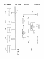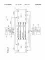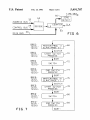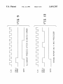
1
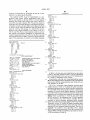
llllllllllllllIllll|||Illllllllllllllllllllllllllllllllllllllllllllllllllll
US005491787A
United States Patent [19]
[11]
Patent Number:
Hashemi
[45]
Date of Patent:
[54] FAULT TOLERANT DIGITAL COMPUTER
4,466,098
[75] Inventor: Seyed H. Hashemi, Mission Viejo,
Southard ................................... .. 371/9
Shung
371/9
4,924,494
5/1990
. . . . . . . . ..
. . . . ..
379/100
5,325,517
6/1994 Baker et a1. ..
5,398,329
3/1995 Hirata et al. .......................... .. 395/575
395/575
Primary Examiner—Hoa T. Nguyen
Calif.
Assistant Examiner—Alan M. Fisch
Attorney, Agent, or Firm—Charles .l. Fassbender; Mark T.
[73] Assignee: Unisys Corporation, Blue Bell, Pa.
Starr; Robert R. Axenfeld
ABSTRACT
[57]
In a multiprocessor system, at least one processor is acting
as a master processor and another processor is acting as the
G06F 11/00
slave or shadow processor that checks operation of the ?rst
U.S. Cl. ....................................................... .. 395/182.09
[581
Feb. 13, 1996
4,610,013 10/1986 Long et a1.
SYSTEM HAVING TWO PROCESSORS
WHICH PERIODICALLY ALTERNATE AS
MASTER AND SLAVE
[21] Appl. No.: 296,302
Aug. 25, 1994
[22] Filed:
1511 Int. GL6 .................................................... ..
8/1984
5,491,787
processor. Periodically, a controller switches operating
Field of Search ................................... .. 395/575, 425;
mode of a master or main processor to slave or shadow
371/681, 16.1, 9.1
mode, and at the same time switches operation of a slave or
shadow processor to main or master processing mode. The
?rst processor is then used as a slave or shadow processor to
[56]
References Cited
check operation of the second processor.
U.S. PATENT DOCUMENTS
3,795,800
4,358,823
3/1974 Nimrno.
11/1982 McDonald et a1. ................... .. 364/200
4o\
1 Claim,6Drawing Sheets
TIMER
K24
TIME-BUT
ERREIR
38/ REPEIRTING/
HANDLING
ERR1
l
13
\
INTR
l
ERRa
+
14
25
ERR
INTR
< INSTRUCTIUN BUS
CUNTRUL Bus
RRoc 1
4
V
\ >
/
INTR
ERR
28\
30
< DATA BUS
>
RRoc a
\ b
32
TESTI BREo
ll
BGNT
<ADDRESS BUS
1+
BGNT
BREo TESTE
A
11
l
v
CDNTRULLER ~—\34
‘SWITCH
TIMER
oR
EVENT
-V3e
A
U.S. Patent
Feb. 13, 1996
Sheet 1 of 6
5,491,787
>
/@,m245,2\?
mmk
wk
25 086
‘EOWMTwS:GHUE
:mm23
:75 Wm8[Wm
mm)U
L
H
_
mE G:.
|._
OH
m325213 $59?
US. Patent
Feb. 13, 1996
Sheet 3 0f 6
5,491,787
48
F I G -4
‘
ELK
\ zERD
'
DETECT
LD <————-—--——>
COUNTER
42
v
32
ADDRESS BUS [
K
46
28
CBNTRUL BUS I
SWITCH
REGISTER
DECUDE _’ LD
K
44
DATA BUS
/
30
32
ADDRESS BUS
\
28
CIIINTRUL BUS
\
DEcDDER.
5O
ERR1
\
CLKT
——> REG
CLK
:Q.
EBB-L» REG
CLK
54
i
i
LD
CLR
ERRDR REG
\
\52
TIME-BUT
5e
F55
REG ‘
FIGS
E\E>O
DATA BUS
30:
INTR
US. Patent
Feb. 13, 1996
Sheet 4 0f 6
5,491,787
TIME-DDT
ee\
ET——>RD
_,, Z
e2
32
ADDRESS BUS Z
)
DETECT
28
CUUNTER
CUNTRDL BUS I
DECUDE "’ LU
K
30
DATA BUS
CLK
e4
\
F1G_6
R
_
4
§E§%‘1_
MASTEREPRDC 1 1
TESTE
SLAVEIPRUC 2]
ITCH
58
?§§$1_
[ START
SWITCH ]/70
TESTB
PRUCESS
‘ BGRT
BRELTJ
1 [
T2_
BREQ}
T2-
STITCH
END
ITCH
PR
SS
RT
§E§$g
MASTERtPRElC 21
TEST2_
SLAVEEPRUC l 1
ITCH
BREO
T1
’
Ta_
START SWITCH
75
‘/78
‘ BERT
153T;
’
EST
r
‘
r
TEsTa
k
TEE?“ _
FIG_7
74
PRUCESS
BREO
BR
]/ 72
SWITCH
END
PR
$
ITCH
33
BERT
‘/8O
J
‘
,
/8E’
US. Patent
Feb. 13, 1996
Sheet 6 0f 6
5,491,787
o_-m:uA
mdHLA
mIhwUzFQuZiMeHlqaE
mo93¢zwUHQ5EmnIa
_MPZH
v75
\Em m m
~|WIlZ|H
v76
5,491,787
1
2
FAULT TOLERANT DIGITAL COMPUTER
SYSTEM HAVING TWO PROCESSORS
WHICH PERIODICALLY ALTERNATE AS
MASTER AND SLAVE
checks operation of the ?rst processor. However, if the
second processor is itself not operating properly, then faults
A portion of the disclosure of this patent document
contains material which is subject to copyright protection.
systems. In effect, the second processor is shadowing the
operation of the ?rst processor, and for that reason is
The copyright owner has no objection to the facsimile
sometimes referred to as a shadow processor. This can be
with the ?rst processor would not be detected. The present
invention ful?lls this need.
Slave or shadow processors are used in fault tolerant
accomplished in several ways, with the mode selected being
dependent on the type of processors being used. For
reproduction by anyone of the patent document or the patent
disclosure, as it appears in the U.S. Patent and Trademark
Of?ce patent ?les or records, but otherwise reserves all
example, an external error compare circuit could be used to
compare the outputs of the two processors. Other processors
copyright rights whatsoever.
can shadow like processors within its own physical package
without a need for external compare circuits. In the latter
FIELD OF THE INVENTION
The present invention relates to fault tolerant digital
computer system architecture especially with respect to
ensuring proper processor operation. The present invention
15
also relates to error detection/correction and fault detection/
recovery. The present invention further relates to electrical
computers and data processing systems, and more particu
20
situation, such processors are placed in the shadow mode by
activating an appropriate external pin. This causes the pro
cessor to tri-state, open-circuit or place a high impedance on
its outputs. In shadow mode, the processor compares its
internal output signal(s) to the corresponding external out
put(s) from the main processor, which is also provided to the
shadow processor. Regardless of the mode used, if there is
larly to general purpose programmable digital computer
a mismatch between those signals, then a mismatch error
systems utilizing an architecture with plural (redundant)
should be indicated, by the shadow processor or by an
processors and control of those processors.
System integrity, or the ability to detect incorrect system
operation, is important in many areas of computer applica
tions. Applications where human safety must be assured,
external compare circuit. However, such a system assumes
25
that the shadow processor is operating properly. If this is not
the case, then an error in the ?rst processor can go unde
tected. Furthermore, with a processor that is equipped with
such as air traffic control, aircraft control, or weapons
shadowing capability within itself, there is also a possibility
guidance and control, are examples of systems in which
errors in processing could have catastrophic effects. Other
applications which have less severe consequences and yet
that the shadow processor is working improperly or not
30
working at all, and thus, there is no mismatch error gener
ated. Furthermore, in a situation where it becomes necessary
operating integrity is highly desirable are banking and
highly secure military classi?ed computing and communi
to transfer system or subsystem control from the ?rst pro
cations.
non-operating second processor could be catastrophic.
One method of ensuring system (or subsystem) integrity
cessor to the second processor, switching to a faulty or
35
addresses, data, control signals and instructions. Thus, both
such processors receive the same addresses, data, control
etc., but only the output(s) of the main processor is actually
used for its intended purpose by the system or subsystem it
signals, instructions and clock(s). One of these processors,
sometimes referred to as the main processor or the master
processor, provides normal processing, control, etc. such as
may be needed for a particular application. The other
In a system or subsystem that includes a main processor
and a shadow processor, the main processor performs all of
the operations of some program, and the shadow processor
just runs in parallel with the main processor and compares
its own internal calculations with anything that the main
processor sends out. Thus, the main processor and the
shadow processor each receive the same instructions, data,
involves the checking of operation of a processor such as a
central processing unit (CPU) or a local processor. In each
such case where a redundant processor is used, the main and
redundant processors are similarly connected to receive
45
processor, sometimes also referred to as a shadow processor
or a slave processor, runs in parallel with the ?rst processor
and compares its own internal calculations with anything
that the main processor sends out. To maintain synchroni
zation between the two processors, they must operate with
identical clocks. This can be accomplished by having one
serves or where it resides. The shadow processor is utilized
only for error or fault detection. For example, an identical
program or set of instructions could be provided to both the
main processor and the shadow processor, and both proces
sors then execute those instructions. Both processors
execute all of the instructions in that particular program. As
a result of executing those instructions, the main processor
eventually produces output(s) at its data output(s), and may
processor provide its clock signal to the other, or by driving
also receive data and generate addresses. Meanwhile, the
the clock input(s) of both such processors with the same
shadow processor is performing the same instructions, and
externally generated clock. In such a con?guration, it may
so internally should be generating the same data results, but
be desirable to give the shadow processor control over the 55 does not externally output that data. Thus, whenever a
system or subsystem when an error is isolated to the main or
command in the program directs the processors to produce
master processor. To maintain synchronization, it may be
a data result, only the main processor will send that result
desirable to ?rst halt operation of both processors, and then
out. That result is then received by the shadow processor,
transfer control from one processor to the other. If the output
which compares that result to its own internally generated
from the main or master processor does not correspond with 60 result of what the shadow processor would have sent out in
what is correspondingly generated internally by the slave or
response to that command. Alternatively, this comparison
could be performed externally, but then care must be taken
shadow processor, then an error is present in the system or
subsystem. For fault detection purposes, the second proces
sor is connected in parallel with the ?rst processor, but the
second processor has its outputs disabled such as by being
placed in a test mode. The second processor, by comparing
its outputs to the outputs of the ?rst processor, extensively
so that only the output of one processor at a time is provided
to the system, subsystem or the like. If the system is
65
operating properly, the results determined by the two pro
cessors should be equal or identical; otherwise, something is
wrong with the system. The system may also include a data
5,491,787
3
4
bus, address bus, instruction bus, etc., with the data bus for
example being connected to other modules that produce or
from the ?rst processor after a predetermined period of time
receive data to or from the main processor. For example,
there could be a data memory, a data I/O module, etc.
connected to the data bus. At any one instant in time, any of
these could be putting out an address or data. In another
instant, any of these could be receiving an address or data.
The shadow processor, as its name implies, acts as a shadow,
monitoring what is going on but not putting anything out on
that bus or otherwise not being utilized by the system.
Whenever the main processor puts something out on the bus,
the shadow processor checks it against its own internal
calculations. However, if the shadow processor is faulty or
Other objects, advantages and novel features of the inven
tion will become apparent from the following detailed
description of the invention when considered in conjunction
would produce an error indication.
with the accompanying drawings.
BRIEF DESCRIPTION OF THE DRAWINGS
In the drawings,
FIG. 1 is a simpli?ed block diagram of a system including
two processors;
FIG. 2 is a block diagram of a two-processor system that
accomplishes fault or error detection for both processors
inoperative, then such checking likely could not be per
formed. In such a situation, the main processor is operating,
and the user might believe that the shadow processor is
checking such operation when in fact that checking is not
15
FIG. 3 is a block diagram of one embodiment of a
processor that can be utilized in the present invention;
FIG. 4 is a block diagram of one embodiment of a timer
being accomplished.
Thus, there is a need to perform in~line, real-time check
ing of a shadow processor. The present invention ful?lls this
need.
As used herein, the terms system and subsystem may be
used interchangeably, and the terms slave processor and
shadow processor may be used interchangeably.
according to the present invention;
or event counter that can be utilized to determine when the
mode exchange by the controller of FIG. 2 can be accom
plished;
FIG. 5 is a block diagram of one embodiment of an error
reporting/handling module that can be used in the system of
25
FIG. 2;
SUMMARY OF THE INVENTION
FIG. 6 is a block diagram of one embodiment of a timer
that can be utilized with the error reporting/handling module
Accordingly, an object of the present invention is to
provide apparatus and method for checking for a malfunc
tioning or inoperative shadow or slave processor.
Another object of the present invention is to provide a
of FIG. 5 in the system of FIG. 2;
FIG. 7 is a ?owchart illustrating a method of switching the
two processors of FIG. 2 between master or operating mode
and slave or checking mode;
fault-tolerant master/slave or main/shadow processor con
?guration.
A further object of the present invention is to provide a 35
fault-tolerant system for processing, control, computing, etc.
Still another object of the present invention is to provide
apparatus and method for switching operation or control
FIG. 8 is a waveform timing diagram for signals that can
be received or produced by the apparatus of FIG. 2 during
the operation of FIG. 7;
FIG. 9 is another waveform timing diagram for signals
that can be received or produced by the apparatus of FIG. 2
during another phase of operation of the apparatus of FIG.
2; and
FIG. 10 is still another waveform timing diagram for
from one processor to another.
Brie?y, these and other objects of the present invention
are accomplished by apparatus and method wherein two or
more processors are connected in parallel to receive identi
signals that can be received or produced by the apparatus of
FIG. 2 during still another phase of operation of the appa
cal instructions, control signals, data, addresses, etc.
involved with normal system operation. A controller is
ratus of FIG. 2.
connected to each such processor to control which proces 45
sor(s) are performing the usual computing operations or the
like, and which processor(s) are instead being used for
DESCRIPTION OF THE PREFERRED
EMBODIMENT
Referring now to the drawings, wherein like reference
characters designate like or corresponding parts throughout
one such processor could be utilized for operational pur
poses, and the other processor would be used for checking 50 the several views, there is shown in FIG. 1 a processing
system 10 including a ?rst processor 12, a second processor
operation of the ?rst processor for error or fault detection
14, memory 16, input/output module 18, and peripheral 20,
purposes. For example, a system could include only two
all interconnected by a common bus 22. Other modules can
such processors. The controller would then switch those two
be connected to bus 22, or any or all of modules 16, 18 and
processors between normal and shadow operation, so that at
checking operation of the other processor(s). For example,
diiferent times each processor would be checking operation
of the other processor. Such switching could be periodic
(e.g. once every second), event-controlled, or both. In this
manner, operation of both such processors could be checked
and proper system operation could be thereby better assured.
55
Should one of these processors while in shadow or checking 60
20 can be removed, within the practice of the present
invention.
A portion of the system 10 of FIG. 1 is illustrated in FIG.
2 in greater detail. System 24 of FIG. 2 includes ?rst
processor 12 and second processor 14 receiving identical
signals on instruction bus 26, control bus 28, data bus 30 and
mode ?nd an error in the other such processor, then an
address bus 32. Controller 34 controls or sets or determines
appropriate error signal would be produced. Alternatively,
the mode of operation of processor 12 and processor 14, and
the outputs of the two processors could be externally com
in turn is controlled or activated by timer/event counter 36.
pared, and an error signal generated if there is a mismatch.
Timer 36 provides a switching signal SWITCH at appropri
If such an external error check is not provided, then after the 65 ate intervals or events to cause controller 34 to exchange the
controller switches the operating mode for the two proces
operating modes of processor 12 and processor 14. In
sors, a timer can be provided so that absence of any signal
response to the switching signal SWITCH, controller 34
5,49 l ,787
5
6
stops or holds operation of processors 12 and 14 using the
bus request signal BREQ. Processor 12 and processor 14
each respond to the bus request signal with the bus grant
signal BGNT, which is then provided to controller 34. In
response to the bus grant signal, controller 34 then changes
the operating mode signal TESTl which it provides to
processor 12, and changes the operating mode signal TEST2
which it provides to processor 14. For example, if processor
12 is to normally be the main processor and processor 14 is
to be the shadow processor for normal operation, then it is
preferred that controller 34 switch the processor operating
modes at regular intervals for a period of time shorter than
those intervals but long enough to determine whether pro
cessor 14 is operating properly, as will be further discussed
below. However, the duration of system 24 operation with
switched operating modes should be short enough (eg. 250
nanoseconds or ?ve clock cycles) that overall operation of
system 24 and of system 10 is not affected (assuming no
fault is present). Because each processor would then be
shadowing operation of the other processor, at ditferent
times, it is preferred that processor 12 and processor 14 be
the same model processor Although the following descrip
control unit 34. If the current slave processor is not func
tioning (dead processor), then as soon as the current slave
processor becomes the future master processor, error report
ing and recovery unit 38 will detect the fault. Thus, the
maximum duration of an unrecovered error would be one
switching time interval of module 36.
As shown in FIG. 2, the two processors 12 and 14 are
connected to all buses (address bus 32, data bus 30, instruc
tion bus 26 and control bus 28) and signals except for the test
inputs and ER outputs of those processors. For this
example, it is assumed that processor 14 normally serves as
the shadow processor. Controller 34 is connected to the test
input of processor 12 and the test input of processor 14, as
well as the BREQ (bus request) inputs and BGNT (bus
15
controller 34 is also receiving a switching input SWITCH
from a timer/event counter 36. The error reporting/recovery
unit 38 receives the ERR1 signal from processor 12, and the
ERR2 signal from processor 14, as inputs, and generates an
INTR non-maskable interrupt signal as output to the pro
cessors. Error reporting/handling module 38 also receives as
an input a TIME-OUT signal from timer 40 (in effect serving
tion applies to use of an Am29000TM or Am29005TM RISC
as a gross timer or dead-man timer) to indicate time-out
microprocessor as processor 12 and as processor 14, it
should be understood that the practice of the present inven—
tion is not limited thereto, and that the present invention can
errors. As discussed above, for example the system 24 could
25
be practiced with other processors. The Am29000TM and
Arn29005TM 32-bit streamlined instruction processors are
produced by Advanced Micro Devices, Inc. and are
described in Arn29000TM and Am29005TM RISC Micropro
cessors User’s Manual and Data Sheet Rev. 1, 1993 pro
duced by Advanced Micro Devices, Inc., 901 Thompson
Place, PO. Box 3453, Sunnyvale, Calif. 94008-3453.
start with processor 12 as the master processor and processor
14 as the slave processor. As the slave processor, if processor
14 detects a mismatch in the two processors’ output(s), then
processor 14 will provide an error signal ERR2 at its output
ERR to the error reporting/recovery unit 38. The error
recovery unit 38 ?rst logs the error. Error recovery unit 38
then tries to put the two processors 12 and 14 back in
synchronization by generating a non-maskable interrupt
signal INTR which is provided to the respective NMI input
As shown in FIG. 2, system 24 also includes error
reporting/handling module 38, which would receive and
grant) outputs of the two processors. At the same time,
35
respond to any error indication produced by processor 12 or
processor 14. For the system of FIG. 2, such error signals
would be produced by processor 12 or processor 14 as error
signal ERR which would be provided to error reporting/
handling module 38. If necessary, as discussed below, error
reporting/handling module 38 would respond with a non
maskable interrupt signal INTR to both processor 12 and
processor 14 to halt and restart their operation because of a
detected fault condition. During a temporary switch of
of each processor. This interrupt causes the two processors
12 and 14 to restart at a speci?c, predetermined address and
thus will be synchronized once again. This restart address
can usually be hardwired within most processors.
FIG. 4 shows one example of a timer/event counter that
can be utilized as timer/event counter 36 in FIG. 2. The
timer/event counter of FIG. 4 includes a decoder 42 con
nected to address bus 32 and control bus 28, a register 44
connected to decoder 42 and data bus 30, a counter 46
connected to register 44, and a zero-value detector 48
connected to counter 46. Register 44 and counter 46 also
operating mode between processor 12 and processor 14 by 45 receive a suitable clock signal, which is preferably the same
controller 34, should not even a good signal appear on error
clock signal that is used to clock processors 12 and 4. When
line ERR1 from processor 12, which would then be func
triggered by a control signal provided by the master pro
tioning as the shadow processor, during a predetermined
cessor on control bus 28, decoder 42 decodes the address
period set by timer 40, then timer 40 would provide a signal
signal then on the address bus. If that address is a particular
TIME-OUT to error reporting/handling module 38. The
address preset for this purpose, then decoder 42 will provide
TIME‘OUT signal would then cause module 38 to generate
an appropriate signal to the load or LD input of register 44.
a non-maskable interrupt INTR because generation of the
This causes register 44 to load the value then appearing on
TIME-OUT signal would indicate that processor 14 is not
data bus 30. This value, which is also provided by the master
functioning.
Processing system 24 includes two processors 12 and 14
processor, dictates the time between switching operating
55
as master and slave connected together in all but a few
signals. System 24 also includes an error reporting and
recovery unit 38 as well as a control unit 34 for master and
slave operation (shadow controller). Control unit 34 indi
cates which one of the processors 12 or 14 is at any one time 60
to be the master processor and which is then to be the slave
processor. Control unit 34 also switches this con?guration
either by an external event or at speci?c time intervals, as
mode of the two processors 12 and 14 between master and
slave. Register 44 and counter 46 each have a parallel load.
The master processor initially loads a value (dictating the
time between switching of the two processors 12 and 14) in
the register. The decode logic 42 will act on the processors
addressing register 44. Since at startup counter 46 would
have a zero value, zero detector 48 will provide a load signal
to the LD input of counter 46. Accordingly, the value now
entered in register 44 is also loaded into counter 46. The
determined by module 36. This switching operation causes
clock signal CLK then causes counter 46 to count down.
the current master processor to become the future slave 65 When the counter counts down to a zero value, the zero
processor, and causes the current slave processor to become
detect hardware 48 will activate the SW’ITCH signal, which
the future master processor, after each switching event by
is provided to controller 34. At the same time, Zero detector
5,491,787
7
8
48 also causes counter 46 to reload the value in register 44
back into the counter. Thus, the interval between successive
switch signals from timer/event counter 36 is held constant,
unless the master processor changes the value held in
the current master processor 12 or 14 is not dead. Control
bus 28 controls decoder 62 by informing decoder 62 when
it is to decode the address provided to the decoder by address
bus 32. If the decoded value from address bus 32 is the value
or values preselected for the purpose, then decoder 62 will
activate the load input LD of counter 64, causing counter 64
register 44. The length of this interval is determined by the
value placed in register 44 and the speed of the clock signal
applied to register 44 and counter 46. Although a zero
detector 48 is shown in FIG. 4, it should be understood that,
within the practice of the present invention, counter 46 can
to load what is then on data bus 30. This value in counter 64
is then counted down by the clock signal CLK. When the
counter reaches a zero value, this is detected by zero detector
be made to count up or down between any two predeter
66 which in response generates the TIME-OUT signal. Thus,
the value loaded into counter 64 determines the delay
provided by the timer of FIG. 6. As discussed above, counter
mined values.
One embodiment of an error reporting/handling module
64 could instead be set to count up or down between any two
that could be utilized as error reporting/handling module 38
of FIG. 2 is shown in FIG. 5. The error reporting/handling
preset values for the same purpose.
module of FIG. 5 includes two registers 50 and 52 feeding 15
Every time that timer/event counter 36 produces signal
an OR gate 54, a third register 56, an error register 58
SWITCH, controller 34 will start to switch the operating
receiving the outputs of OR gate 54 and register 56, and a
modes between the master processor and the slave proces
decoder 60 for controlling operation of error register 58.
sor. This process is illustrated in FIGS. 7 and 8. As shown
Registers 50, 52, S6 and 58 have a common clock, prefer
in FIG. 7, this process starts at step 70 with controller 34
ably the clock used for processor 12 and processor 14. 20 responding to the SWITCH signal by applying an active bus
Register 50 receives and holds the ERRl output of processor
request signal to the BREQ input of processor 12 and the
12. Register 52 receives and holds the ERR2 output of
BREQ input of processor 14. This bus request signal will
processor 14. Register 56 receives and holds the TIME-OUT
stop the ?ow of instructions as well as data transactions
output of timer 40. OR gate 54 combines the registered
within a few clock cycles of processors 12 and 14. At this
ERRl and ERR2 outputs into a single error signal which is 25 time, processors 12 and 14 release all of their buses 26, 28,
provided as an input to error register 58. Register 56
30 and 32 by tri-stating them. Processor 12 and processor 14
provides the registered TIME-OUT signal as another input
inform controller 34 of this action by each providing an
to error register 58. The master processor, via address bus 32
appropriate bus grant signal BGRT from their respective
and control bus 28 as decoded by decoder 60, controls
BGNT outputs to controller 34. Upon being so informed,
whether error register 58 will load the value being provided 30 controller 34 at step 72 then switches the operating modes of
thereto onto data bus 30, or whether error register 58 would
the two processors 12 and 14 by changing the state of their
instead be cleared. An appropriate signal or value on control
respective TEST input. In other words, at step 72 the signal
bus 28 from the master processor enables decoder 60 to
previously applied by controller 34 to the TEST1 input of
decode the value on address bus 32. In the apparatus of FIG.
processor 12 is now instead applied to the TEST2 input of
5, the two ERRl and ERR2 signals are registered and 35 processor 14, and vice versa. Controller 34 at step 74 then
combined together and saved into the error register. At the
removes the bus request signal, and processors 12 and 14
same time, if timer 40 produces a TIME-OUT signal, then
start where they left oiT, but with reversed roles. In other '
the TIME-OUT signal is instead registered and saved into
words, if processor 12 was previously the master processor
the error register. The master processor is able to read the
and processor 14 was previously the slave processor, then at
error register 58 via data bus 30 and take proper action. The 40 step 74 processor 12 is now instead operating as the slave
master processor would then clear error register 58 via
processor while processor 14 is then instead operating as the
address bus 32 and control bus 28 as decoded by decoder 60.
master processor. Steps 68 through 74 take only a few
If any of an ERRl error, an ERR2 error or a TIME-OUT
processor clock cycles, and can be repeated as often as
error occurs, then error register 58 generates an appropriate
needed. If the current slave processor is not fimctioning,
signal on its output lNTR which is applied as a non
then after the switch provided by steps 68 through 74 it
maskable interrupt to the NMI input of processors 12 and
140 This INTR signal would then activate the non-maskable
interrupt of processors 12 and 14, which in turn resynchro
nizes processors 12 and 14 again. Thus, the apparatus of
FIG. 5 is a self-locking mechanism.
One embodiment of timer 40 is shown in FIG. 6. The
becomes the new master processor. ‘The new master proces
sor will then either function with a mismatch which is
signalled by the new slave processor immediately, or else
cannot function at all which timer 40 will catch by an
50
appropriate TIME-OUT signal after the preset waiting time
a counter 64 and a zero detector 66. The master processor 12 55
expires. The maximum time that the system 24 can be
exposed to a faulty shadow processor is thus the time
between switching. After the roles of processors 12 and 14
have been reversed for a predetermined period, shadow
controller 34 will then unreverse the processor 12 and 14
timer of FIG. 6 is similar to the timer/event counter of FIG.
4 except that the register 44 of FIG. 4 is not needed in the
timer of FIG. 6. The timer of FIG.‘ 6 includes a decoder 62,
or 14 controls the timer of FIG. 6 via address bus 32 and
control bus 28, which are provided as inputs to decoder 62.
The output of decoder 62 in turn is applied to the load input
LD of counter 64. Data bus 30 is connected to the data input
of counter 64. Counter 64 is loaded every time that the
roles using steps 76 through 82, which respectively corre
spond to steps 68 through 74. With step 74, the bus request
master processor 12 or 14 writes a value to it. If the current
sor 12 and processor 14 as discussed above. When proces
master processor is hung and can not reload counter 64, then
counter 64 reaches zero, and zero detect hardware 66 will
sors 12 and 14 respond with the bus grant signal, controller
34 again reverses the states of the TEST1 and TEST2
signals, so that processor 12 is again the master processor
and processor 14 is again the slave processor. At step 82, the
switch process ends with the removal or inactivation by
controller 34 of the bus request signal, which is followed by
signal is no longer active. When timer/event counter 36
provides another SWITCH signal to controller 34, then at
step 78 controller 34 applies a bus request signal to proces
then produce an appropriate TIME-OUT signal. The TIME
OUT signal is applied as an input to the error reporting!
handling module. In FIG. 5, the TIME-OUT signal is
applied to register 56. Thus, the timer of FIG. 6 ensures that
65
5,491,787
9
10
removal or inactivation by processors 12 and 14 of their
-continued
respective bus grant signals (step 68).
endwith;
The method of FIG. 7 can be implemented in a pro
else E_SWI with
breq I 0;
grammed logic device (PLD), programmed logic array
testl : I;
test2 = 0;
(PLA), state machine or the like. FIG. 7 is a flow diagram
showing what setup inputs would cause such a device to
move from one state to another. FIG. 7 shows the respective
endwith;
STATE M2_Sl:
if switch then S_SW2 with
breq : 1;
inputs that cause such state changes, what happens internally
in response to each such input and how the signals produced
testl = I;
test2 = 0;
by such a device would be affected. One such device that
could be used for this purpose is a 22V10 PLD device.
endwith;
else M2_Sl with
However, the present invention is not limited to use of a
22V10; any PLD, PLA or state machine could be used for
breq = O;
testl : l;
test2 = O;
this purpose. The Boolean statements or expressions that
would be implemented in such a PLD or the like to provide
endwith;
STATE SfSWZ:
if bgnt then SW2 with
controller 34 is given in Table 1 below and in the following
pages. These statements are written in the ABEL language.
module SHADOW
SHADOW device
switch
PIN;
bgnt
breq
PIN;
PIN;
testl
test2
PIN;
PIN;
qO
ql
q2
clk
breq : I;
testl = 0;
test2 = I;
‘b22v10‘;
20
endwith;
else S_SW2 with
breq = l;
testl : 1;
test2 = 0;
endwith;
25
PIN;
PIN;
PIN;
STATE SW2:
goto E_SW2 with
breq = 0;
testl = 0;
test). = J;
PIN;
H,L,X,Z,CK : l,O,.X.,.Z.,.C.;
endwith;
“STATE DEFINITIONS"
30
MI_S2 = [ O, O, 0];
S_SWI = [ O, O, I];
SW1 = [ O, l, 0];
EWSWI = [0, I, 1];
“MASTER PROCI & SLAVE PROCZ”
“START SWITCHING"
“SWITCH IN PROGRSS"
“END SWITCH”
“MASTER PROCZ & SLAVE PROCI"
“START SWITCI-HNG"
STATE E_SWZ:
if !bgnt then Ml_S2 with
breq = 0;
testl = 0;
test2 : l;
endwith;
35
else EASWZ with
breq = 0;
“SWITCH IN PROGRESS”
“END SWITCH”
testl = O;
test2 : 1;
endwith;
end
“STATE MACHINE"
STATE?DIAGRAM shad_sw;
STATE Ml_S2:
In Table 1, all states have been identi?ed as has been done
in FIG. 7. The state machine of Table 1 can be programmed
if switch then S_SWI with
breq = l;
into a programmable device such as a 22V10 manufactured
testl = 0;
test2 : l;
endwith;
else MIWSZ with
45
breq : 0;
logic devices (PLDs), programmable logic arrays (PLAs),
testl = 0;
test2 : l;
state machines or the like.
endwith;
STATE S_SWl:
if bgnt then SW1 with
by a variety of integrated circuit vendors.
Alternatively, timer 36, error reporting/handling module
38 and timer 40 could also be implemented in programmable
FIG. 8 is a waveform timing diagram showing signal
50
changes during a switch or exchange of master processor
and shadow processor roles or modes. Initially, starting from
the left of FIG. 8, the initial master processor is identi?ed as
processor P1, and the initial shadow processor is identi?ed
55
breq : O;
processors are then halted (here using the bus request signal
BREQ which is responded to with the bus grant signal
BGNT) at time T1. At subsequent time T2, after operation
of both processors has been halted, controller 34 then
proceeds to switch processor operating modes between
master and shadow by changing signals TESTI and TEST2.
testl : l;
test2 : O;
Thereafter, at time T3, system 24 begins operating again,
breq : l;
testl = I;
testZ : 0;
endwith;
as processor P2. To cause a switch in processor modes, both
else SWSWI with
breq : l;
testl : O;
test2 : 1;
endwith;
STATE SW1:
goto E_SWL with
with processor P2 now being the master processor and with
processor P1 now being the shadow processor. The clock is
endwith;
STATE E_SWl:
if lbgnt then M2_Sl with
breq : 0;
testl : l;
test2 = 0;
65
preferably the common clock described above. Signal
BGNT is provided by processors 12 and 14 to controller 34.
Signals BREQ, TESTI and TEST2 are provided by control
ler 34 to processors 12 and 14.
5,491,787
11
12
FIGS. 9 and 10 are waveform timing diagrams for when
lines, except MSERR, being forced to the high-impedance
an error condition is detected. FIG. 9 shows the alignment or
realignment process after a mismatch error is reported to
the result of the comparison of processor outputs with the
state or tri-state. The master/slave error output signal shows
module 38. FIG. 10 shows the shadow processor reporting
signals provided internally to off-chip drivers of the slave
a bad or dead master processor. FIG. 9 shows a signal 5
processor. If there is a difference for any enabled such driver,
then this line is asserted. A high-to-low transition on the
WARN input causes a non-maskable trap or interrupt to
sequence when an error is detected. During operation of
system 24, if the shadow processor gets a result that does not
correlate with the corresponding result provided by the
occur.
master processor, then the shadow processor reports this
error as signal ERRl (from processor 12) or ERR2 (from
processor 14) to error reporting/handling module 38. A
However, as discussed above, the present invention is not
limited to utilization of the Am29000/OO5 microprocessor.
Instead, processors produced by Intel Corporation, Motorola
Corporation, etc. running in parallel could be substituted
non-maskable interrupt INTR is then generated to resyn
chronize processors 12 and 14. System 24 then tries to
continue operating with the hope that the detected error was
just a transient error or a temporary glitch. However, if
immediately or shortly thereafter (such as is shown in FIG.
10) the error signal recurs, then a faulty or inoperative
master processor is indicated.
In FIG. 10, presence of a faulty master processor is
indicated by repeated presence of error indications or signals
on signals or lines ERRl or ERR2 every few clock cycles.
therefor.
It is preferred that processor 12, processor 14, timer or
event counter 36, controller 34, error reporting/handling
module 38 and timer 40 all utilize a common clock.
The timer or event counter of FIG. 4 is a pre-loaded
programmable timer, providing a repeated switching signal
to switch processors 12 and 14 between master and slave
20
Ifthat occurs, then the command or level for a non-maskable
interrupt will remain on output line or signal INTR for at
least a relatively extended duration, at least longer than is
shown in FIG. 9. If system 10 is con?gured to be operable
without a shadow processor, then it would be preferred to
turn 011’ or deactivate the bad processor, and continue system
operation with only the good processor(s) operating. This
25
modes and back. The frequency of such switching depends
on the criticality of knowing promptly if the shadow pro
cessor is bad or malfunctioning. For example, a complete
switching cycle between master and slave mode and back
again could be done once every minute, or once every
second, or each time that an input/output event occurs.
Switching could occur with each I/O event for example if the
master processor is calculating the physical location of
received or produced data. Reading the wrong data from the
wrong location, or storing data in the wrong location, are
obviously not desirable. For some applications, even if the
shadow processor 14 or 12 is not working, system 24 (and
can be accomplished by inserting an AND gate on the
SWITCH line from timer 36 to controller 34. This AND gate 30
would then be controlled by what is normally a master
system 10) are not dead if the master processor 12 or 14 is
processor, which could thereby remove signal SWITCH and
still
working. Knowing the status of the shadow processor
disable controller 34. Alternatively, the master processor
immediately
would then not be so critical, although reason
could disable controller 34 by loading register 44 with a
ably
prompt
status infonnation would be needed to avoid
35
large value. However, if an operative shadow processor is
future
problems.
However, if for the particular application,
needed for system 10 operation, and no backup shadow
proper
operation
of the shadow processor, to check the
processor is available in the system, then it would be
master processor, would be vital to maintaining system 24
preferred to shut down all or part of system 10.
integrity, then the frequency of switching processor modes
As discussed above, processor 12 and processor 14 can
should be increased appropriately.
40
for example each be an Am29000/005 microprocessor. A
simpli?ed block diagram, adapted from FIG. 2—2 of the
Registers 44, 50, 52, 56 and 58 can for example each be
a standard or ordinary register.
AMD manual cited above, is shown in FIG. 3. As shown in
FIG. 3, each such processor includes an instruction fetch
unit 84 receiving instructions from instruction bus 26, and an
Some of the many advantages of the invention should
now be readily apparent. For example, apparatus and
execution unit 86 receiving instructions from instruction
method have now been provided for checking for a dead
fetch unit 84 and receiving or producing data on a separate
shadow processor, such as when an error is in the shadow
processor so that it cannot check the master processor. Timer
data bus 30. The Am29000 microprocessor furthermore
includes memory management unit 88 which produces
36 periodically produces a switching or clock pulse, for
address signals; otherwise, addresses would be sent to or
example once every second or so, to controller 34, which in
turn sends appropriate control signals to the two processors
which put the main processor and the shadow processor in
a hold state where they do not do anything, to maintain
request (input, synchronous) signal BREQ would corre
synchronization.
Controller 34 then puts out other control
spond to signal BREQ described above, bus grant (output,
signals which switch the main processor to shadow mode
synchronous) signal BGRT would correspond to signal 55 and the shadow processor to main processor mode. Control
BGNT described above, master/slave error (output, synchro
ler 34 then instructs the two processors to start executing
nous) signal MSERR corresponds to signals ERRI and
again. The main processor is now serving as the shadow
ERR2 described above, test mode (input, asynchronous)
processor, to check the processor that had, prior to this
signal TEST corresponds to signals TESTl and TEST2
switch, been functioning as the shadow processor. If the
described above, and warn (input, asynchronous, edge
former shadow processor is faulty or dead, and the main
sensitive) signal WARN corresponds to signal INTR
processor is operating properly, that situation could other
described above. The bus request input allows other masters
wise have continued inde?nitely. However, with the oper
to arbitrate for control of the processor channel. The bus
ating mode exchange provided by the present invention, the
grant output signals to an external master that the processor
main processor would now be able to detect faulty output of
is relinquishing control of the channel in response to the bus 65 the shadow processor, which would then be reported to error
request signal. When the test mode input is active, the
reporting/handling module 38. A fault-tolerant master/slave
processor is in test mode, with all outputs and bi-directional
or main/shadow con?guration is thereby provided.
produced by execution unit 86. For these AMD micropro
cessors, as described in the above-identi?ed manual, bus
5,491,787
13
14
Obviously, many modi?cations and variations of the
present invention are possible in light of the above teach
ings. It is therefore to be understood that the foregoing
interval where said ?rst processor is in said master
mode and said second processor is in said slave mode;
running said system in an opposite state for another
predetermined time interval where said second proces
embodiments are presented by way of example only and
that, within the scope of the appended claims and equiva
lents thereto, the invention may be practiced otherwise than
as speci?cally described.
What is claimed is:
1. A method of operating a fault tolerant digital computer
system of the type which includes ?rst and second proces
sors with each such processor having a) a standalone master
operating mode and b) a slave mode for monitoring the other
processor, said method comprising the steps of:
running said system in one state for a predetermined time
sor is in said master mode and said ?rst processor is in
said slave mode; and,
periodicly switching the operation of said system from
10
said one state to said opposite state, and vice-versa,
such that said ?rst and second processors are in said
master mode during respective time intervals which are
interleaved