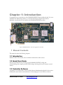
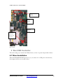
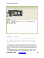
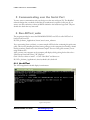
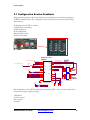
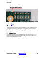
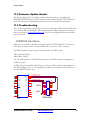
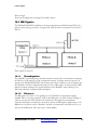
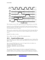
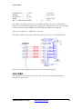
1
LOGIC Emulation Source
User Guide
DN9002K10PCIE8T
DN9002K10PCIE8T User Manual
Major Revision 1
Last Update April 13, 2009
7469 Draper Avenue
La Jolla, CA92037 USA
Phone 858.454.3419 • Fax 858.454.1279
[email protected]
www.dinigroup.com
DN9002K10PCIE8T User Guide
www.dinig
1 Table of Contents
Contents
1
TABLE OF CONTENTS.......................................................................................... 3
CHAPTER 1: INTRODUCTION .................................................................................... 1
1
MANUAL CONTENTS............................................................................................ 1
1.1
1.2
1.3
1.4
1.5
1.6
2
INTRODUCTION ........................................................................................................ 1
QUICK START GUIDE............................................................................................... 1
CONTROLLER SOFTWARE........................................................................................ 1
HARDWARE ............................................................................................................. 2
THE REFERENCE DESIGN ........................................................................................ 2
ORDERING INFORMATION ....................................................................................... 2
CONVENTIONS........................................................................................................ 2
2.1 TYPOGRAPHICAL ..................................................................................................... 2
2.2 MANUAL CONTENT ................................................................................................. 2
2.2.1 File names ......................................................................................................... 2
2.2.2 Physical Dimensions ........................................................................................ 2
2.2.3 Part Pin Names ................................................................................................. 3
2.2.4 Schematic Clippings ......................................................................................... 3
2.3 TERMINOLOGY ........................................................................................................ 3
3
RESOURCES ............................................................................................................. 4
3.1 USER CD ................................................................................................................. 4
3.2 DINIGROUP.COM ...................................................................................................... 5
3.3 ERRATA AND CUSTOMER NOTIFICATIONS.............................................................. 5
3.3.1 Existing Errata.................................................................................................. 5
3.4 SCHEMATICS AND NETLIST ..................................................................................... 6
3.4.1 Netlist................................................................................................................. 6
3.4.2 Net name conventions....................................................................................... 6
3.5 DATASHEET LIBRARY ............................................................................................. 6
3.6 XILINX ..................................................................................................................... 6
3.7 DINI GROUP REFERENCE DESIGNS ......................................................................... 7
4
EMAIL AND PHONE SUPPORT .......................................................................... 7
CHAPTER 2: QUICK START GUIDE ......................................................................... 9
1
PROVIDED MATERIALS ...................................................................................... 9
DN9002K10PCIE8T User Guide
www.dinig
I N T R O D U C T I O N
1.1
2
SYSTEM REQUIREMENTS ......................................................................................... 9
WARNINGS .............................................................................................................10
2.1
2.2
2.3
3
ESD .......................................................................................................................10
OTHER ...................................................................................................................10
OTHER WARNINGS .................................................................................................10
PRE-POWER ON INSTRUCTIONS ...................................................................11
3.1 INSTALL MEMORY.................................................................................................11
3.2 PREPARE CONFIGURATION FILES ...........................................................................11
3.3 INSERT THE COMPACT FLASH CARD INTO THE DN9002K10PCIE8T’S COMPACT
FLASH SLOT.......................................................................................................................12
3.4 INSTALL DN9002K10PCIE8T IN COMPUTER ......................................................12
3.5 CABLES ..................................................................................................................12
3.5.1 Connect RS232 Cable.....................................................................................12
3.5.2 Connect USB Cable ........................................................................................13
3.5.3 Connect Power cable......................................................................................13
3.6 VIEW CONFIGURATION FEEDBACK OVER RS232 ..................................................13
3.7 CHECK LED STATUS LIGHTS .................................................................................15
4
RUN USB CONTROLLER....................................................................................16
4.1 DRIVER INSTALLATION .........................................................................................16
4.2 OPERATING THE USB CONTROLLER PROGRAM ...................................................17
4.2.1 Configure an FPGA........................................................................................18
4.2.2 Set Clock Frequencies ....................................................................................19
4.2.3 Run Hardware Test (DDR2) ..........................................................................19
4.3 GETTING DATA TO AND FROM THE FPGA ............................................................20
5
COMMUNICATING OVER THE SERIAL PORT..........................................21
6
RUN AETEST_WDM.............................................................................................21
6.1.1
7
Use AETest ......................................................................................................21
SCAN THE JTAG CHAIN ....................................................................................23
7.1
MOVING ON...........................................................................................................24
CHAPTER 3: CONTROLLER SOFTWARE ............................................................25
1
USB CONTROLLER..............................................................................................26
1.1 MAIN WINDOW .....................................................................................................26
1.1.1 Refresh Button.................................................................................................27
1.1.2 Disable/Enable USB .......................................................................................27
1.1.3 Log Window ....................................................................................................27
1.1.4 Board Graphic ................................................................................................27
1.2 MENU OPTIONS .....................................................................................................29
I N T R O D U C T I O N
1.2.1 File Menu ........................................................................................................29
1.2.2 Edit Menu ........................................................................................................29
1.2.3 FPGA Configuration Menu............................................................................29
1.2.4 FPGA Reference Design ................................................................................30
1.2.5 Main Bus .........................................................................................................30
1.2.6 Settings/Info Menu ..........................................................................................31
1.2.7 Production Tests .............................................................................................32
1.2.8 Unsupported Features ....................................................................................32
1.3 INI FILE .................................................................................................................32
2
AETEST USB ...........................................................................................................33
2.1 COMPILING AETEST_USB .....................................................................................33
2.1.1 Cygwin.............................................................................................................33
3
PCIE AETEST APPLICATION ...........................................................................33
3.1 FUNCTIONALITY ....................................................................................................33
3.2 RUNNING AETEST ...............................................................................................34
3.3 COMPILING AETEST (PCIE) ................................................................................34
3.3.1 Compiling AETest for Windows XP...............................................................34
3.3.2 Cygwin.............................................................................................................34
4
ROLLING YOUR OWN SOFTWARE ...............................................................35
4.1
4.2
5
USB .......................................................................................................................35
PCIE.......................................................................................................................35
UPDATING THE FIRMWARE ...........................................................................35
5.1 OBTAINING THE UPDATES .....................................................................................36
5.2 UPDATING THE SPARTAN (PROM) FIRMWARE ....................................................36
5.2.1 Using JTAG cable (Xinlinx products) ...........................................................36
5.2.2 Using USBController .....................................................................................38
5.2.3 Using AEtest_USB ..........................................................................................38
5.3 UPDATING EEPROM FIRMWARE (NOT RECOMMEND).........................................39
5.3.1 Using USBController .....................................................................................40
5.3.2 Using AETest_USB.........................................................................................40
5.4 UPDATING THE MCU (FLASH) FIRMWARE ...........................................................41
5.4.1 Using USBController .....................................................................................41
5.4.2 Using AETest_USB.........................................................................................41
5.5 PCI EXPRESS ENDPOINT FIRMWARE ....................................................................42
5.5.1 Using JTAG USB cable (Xilinx products) .....................................................42
5.5.2 Using USBController .....................................................................................45
5.5.3 Using AETest_USB.........................................................................................45
CHAPTER 4: HARDWARE ..........................................................................................47
1
GENERAL OVERVIEW .......................................................................................47
I N T R O D U C T I O N
1.1 MARKETING ..........................................................................................................47
1.1.1 Features...........................................................................................................48
2
VIRTEX 5 .................................................................................................................49
3
CONFIGURATION SECTION ............................................................................49
3.1 CONFIGURATION SECTION FEEDBACK..................................................................50
3.2 FPGA CONFIGURATION ........................................................................................51
3.3 USB AND PCIE INTERFACES .................................................................................52
3.4 COMPACTFLASH INTERFACE ................................................................................52
3.4.1 Main.txt ...........................................................................................................52
3.4.2 Hardware ........................................................................................................55
3.5 CONFIGURATION REGISTERS ................................................................................56
3.5.1 Undocumented controls..................................................................................56
3.6 FIRMWARE .............................................................................................................57
4
CLOCK NETWORK ..............................................................................................57
4.1.1 GC Pins ...........................................................................................................57
4.2 GLOBAL CLOCKS...................................................................................................57
4.3 G0, G1, G2 CLOCKS ..............................................................................................58
4.3.1 Clock Synthesizers ..........................................................................................59
4.4 EXT CLOCKS ..........................................................................................................61
4.4.1 EXT0 ................................................................................................................61
4.4.2 EXT1 ................................................................................................................62
4.4.3 Daughtercard zero-delay mode .....................................................................62
4.4.4 SMA input........................................................................................................62
4.5 PCIE REFCLOCK ....................................................................................................63
4.6 NON-GLOBAL CLOCKS .........................................................................................63
4.6.1 Clock TP..........................................................................................................63
4.6.2 Ethernet Clock ................................................................................................64
4.6.3 DDR2 Clocks ..................................................................................................64
4.6.4 SMA Clock A ...................................................................................................64
5
TEST POINTS..........................................................................................................65
5.1
5.2
5.3
5.4
5.5
5.6
6
POWER THRU-HOLE...............................................................................................65
POWER TP .............................................................................................................66
DIMM POWER ......................................................................................................67
“GC” TEST POINTS ................................................................................................68
CLOCK TEST POINTS ..............................................................................................69
DIMM SIGNALS ....................................................................................................70
USB INTERFACE ...................................................................................................70
6.1 CONNECTING TO THE DN9002K10PCIE8T.........................................................71
6.1.1 Windows XP ....................................................................................................71
6.1.2 Windows Vista.................................................................................................71
I N T R O D U C T I O N
6.1.3 Linux ................................................................................................................71
6.1.4 Communication...............................................................................................71
6.2 VENDOR REQUESTS...............................................................................................72
6.2.1 VR_CLEAR_FPGA ........................................................................................72
6.2.2 VR_SETUP_CONFIG ....................................................................................73
6.2.3 VR_END_CONFIG ........................................................................................73
6.2.4 VR_SET_EP6TC (Read buffer size) ..............................................................73
6.2.5 VR_MEM_MAPPED (Configuration Registers) ..........................................73
6.2.6 Other Vendor Requests...................................................................................73
6.3 MAIN BUS ACCESSES.............................................................................................73
6.3.1 Important Note about Endpoints....................................................................74
6.3.2 Performance....................................................................................................74
6.4 FPGA CONFIGURATION ........................................................................................75
6.4.1 Readback .........................................................................................................75
6.5 USB HARDWARE ..................................................................................................76
6.5.1 Cypress CY7C68013A ....................................................................................76
6.5.2 Activity LED ....................................................................................................77
6.5.3 Configuration FPGA ......................................................................................77
6.5.4 Power ..............................................................................................................77
6.6 TROUBLESHOOTING ..............................................................................................77
6.6.1 USB Controller Freezes .................................................................................77
6.6.2 Main Bus always returns 0x______ (Error Codes) ......................................78
7
PCIE INTERFACE .................................................................................................78
7.1 HOST INTERFACE, ELECTRICAL ............................................................................79
7.1.1 Power ..............................................................................................................80
7.1.2 PCI-X...............................................................................................................81
7.2 HOST INTERFACE, MECHANICAL ..........................................................................81
7.3 PROVIDED “FULL-FUNCTION PCI EXPRESS ENDPOINT” ......................................81
7.3.1 BAR 0 Access ..................................................................................................82
7.3.2 BAR 1-5 Access ...............................................................................................83
7.3.3 DMA Channels 0 and 1 ..................................................................................83
7.3.4 DMA Posted Mode .........................................................................................84
7.3.5 DMA Main Bus ...............................................................................................84
7.3.6 Electrical .........................................................................................................84
7.3.7 Timing..............................................................................................................84
7.3.8 FPGA Interface...............................................................................................85
7.3.9 Host Interface, Software .................................................................................86
7.4 OTHER PROVIDED DESIGNS FOR THE LXT ...........................................................89
7.4.1 No design.........................................................................................................89
7.4.2 PIPE ................................................................................................................90
7.4.3 Slowdown PIPE Core.....................................................................................90
7.5 TROUBLESHOOTING ..............................................................................................91
8
UNUSABLE PINS ...................................................................................................92
I N T R O D U C T I O N
8.1.1
Configuration ..................................................................................................92
9
SYSTEM MONITOR/ADC ...................................................................................92
10
RESET .......................................................................................................................93
10.1 POWER RESET........................................................................................................93
10.2 USER RESET...........................................................................................................94
11
JTAG..........................................................................................................................94
11.1 FPGA JTAG .........................................................................................................95
11.1.1 Compatible Configuration Devices ...............................................................95
11.1.2 ChipScope .......................................................................................................95
11.2 FIRMWARE UPDATE HEADER................................................................................96
11.3 TROUBLESHOOTING ..............................................................................................96
12
RS232 INTERFACE ...............................................................................................96
12.1.1 Configuration RS232 ......................................................................................97
13
TEMPERATURE SENSORS ................................................................................97
14
ENCRYPTION BATTERY ...................................................................................98
15
LED INTERFACE ..................................................................................................99
15.1
15.2
15.3
15.4
15.5
16
CONFIGURATION SECTION LEDS .........................................................................99
USER LEDS .........................................................................................................100
ETHERNET LEDS .................................................................................................100
POWER LEDS ......................................................................................................101
UNUSED LEDS ....................................................................................................102
DDR2........................................................................................................................102
16.1 POWER .................................................................................................................103
16.1.1 Interface Voltages .........................................................................................103
16.1.2 Changing the DIMM voltage .......................................................................103
16.2 CLOCKING ...........................................................................................................104
16.3 SIGNALING ...........................................................................................................105
16.3.1 Standards ......................................................................................................105
16.3.2 Serial Interface..............................................................................................106
16.3.3 Timing............................................................................................................106
16.4 COMPATIBLE MODULES ......................................................................................107
16.5 TEST POINTS ........................................................................................................108
17
FPGA INTERCONNECT. ...................................................................................108
18
MAIN BUS ..............................................................................................................110
18.1 MB SIGNALS .......................................................................................................111
I N T R O D U C T I O N
18.1.1 Disambiguation.............................................................................................111
18.1.2 Electrical .......................................................................................................111
18.1.3 Timing............................................................................................................112
18.2 ERROR CODES .....................................................................................................112
18.3 FPGA INTERFACE ...............................................................................................113
18.3.1 Conventional Memory map ..........................................................................114
19
ETHERNET ...........................................................................................................115
19.1 MII.......................................................................................................................115
19.1.1 Electrical .......................................................................................................115
19.1.2 Timing............................................................................................................116
19.2 JTAG ...................................................................................................................118
20
EPROM ...................................................................................................................119
21
MICTOR CONNECTORS ..................................................................................120
21.1 FPGA B MICTOR ................................................................................................120
21.2 MAINBUS MICTOR ..............................................................................................121
22
POWER ...................................................................................................................123
22.1 POWER 12V .........................................................................................................123
22.2 POWER 3.3V ........................................................................................................124
22.3 POWER 2.5V ........................................................................................................124
22.4 GROUND ..............................................................................................................124
22.5 POWER CONNECTIONS ........................................................................................124
22.6 POWER MONITORS ..............................................................................................125
22.7 HEAT....................................................................................................................126
22.7.1 Fans ...............................................................................................................126
22.7.2 Removing Heatsinks .....................................................................................126
22.7.3 Fan Tachometers ..........................................................................................127
23
CONNECTORS .....................................................................................................127
23.1 FPGA USER INTERFACE CONNECTORS ..............................................................127
23.1.1 Comments......................................................................................................128
23.2 NON-FPGA USER INTERFACE CONNECTORS .....................................................128
23.2.1 Comments......................................................................................................129
23.3 NOT-FOR-USE CONNECTORS..............................................................................129
23.3.1 Comments......................................................................................................130
24
MECHANICAL .....................................................................................................130
25
DAUGHTERCARD HEADERS .........................................................................131
25.1 DAUGHTER CARD PHYSICAL ..............................................................................132
25.1.1 Daughter Card Locations and Mounting ....................................................133
25.1.2 Standard Daughtercard Size ........................................................................134
I N T R O D U C T I O N
25.1.3 Insertion and removal...................................................................................135
25.2 DAUGHTER CARD ELECTRICAL ..........................................................................137
25.2.1 Pin assignments ............................................................................................142
25.2.2 CC, VREF, DCI ............................................................................................144
25.2.3 Global clocks ................................................................................................144
25.2.4 Timing and Clocking ....................................................................................144
25.2.5 Power and Reset ...........................................................................................145
25.2.6 VCCO Voltage ..............................................................................................146
25.2.7 VCCO bias generation .................................................................................146
25.3 ROLLING YOUR OWN DAUGHTERCARD ...............................................................147
26
TROUBLESHOOTING .......................................................................................147
26.1
26.2
26.3
26.4
26.5
THE BOARD IS DEAD ............................................................................................147
THE FPGAS WON’T PROGRAM............................................................................148
MY DESIGN DOESN’T DO ANYTHING ...................................................................148
THE DCMS WON’T LOCK ....................................................................................149
THE SIGNAL ON MY BOARD IS GOING CRAZY ON MY OSCILLOSCOPE..................149
CHAPTER 5: REFERENCE DESIGN ......................................................................151
1
PURPOSE ...............................................................................................................151
1.1
2
INTERFACES USED BY REFERENCE DESIGN..........................................................151
HARDWARE TESTS ...........................................................................................152
2.1.1
2.1.2
2.1.3
2.1.4
2.1.5
2.1.6
3
Testing PCI Express interface......................................................................152
Testing FPGA-to-FPGA interconnect .........................................................152
Testing DDR2 Interfaces ..............................................................................152
Testing USB ..................................................................................................153
Testing Ethernet ............................................................................................153
Testing Daughtercard Connectors ..............................................................153
REFERENCE DESIGN TYPES .........................................................................153
3.1
3.2
3.3
3.4
3.5
3.6
4
MAIN TEST ..........................................................................................................153
LVDS ..................................................................................................................154
SINGLE FAST........................................................................................................154
V5 INTERCONNECT..............................................................................................154
ETHERNET............................................................................................................154
HEADER ...............................................................................................................154
USING THE REFERENCE DESIGN................................................................154
4.1
5
REFERENCE DESIGN MEMORY MAP ...................................................................154
INTERCONNECT (SINGLE) .............................................................................156
5.1
5.2
USING THE DESIGN ..............................................................................................157
RUNNING THE TEST .............................................................................................157
I N T R O D U C T I O N
6
DDR2 INTERFACE ..............................................................................................157
6.1
6.2
6.3
PROVIDED FILES ..................................................................................................158
USING THE DESIGN ..............................................................................................158
RUNNING THE TEST .............................................................................................158
7
CLOCK COUNTERS ...........................................................................................158
8
LEDS ........................................................................................................................158
9
SIMULATING THE REFERENCE DESIGN .................................................159
10
COMPILING THE REFERENCE DESIGN....................................................159
10.1.1 The Xilinx Embedded Development Kit (EDK) ..........................................159
10.1.2 Xilinx ISE ......................................................................................................159
10.1.3 The Build Utility: Make.bat..........................................................................160
10.2 BITGEN OPTIONS .................................................................................................160
11
LVDS REFERENCE DESIGN............................................................................161
11.1 PROVIDED FILES ..................................................................................................161
11.2 USING THE DESIGN ..............................................................................................161
11.3 RUNNING THE TEST .............................................................................................162
12
PCIE INTERFACE REFERENCE DESIGN ...................................................162
12.1 PROVIDED FILES ..................................................................................................162
12.2 USING THE DESIGN ..............................................................................................162
12.3 RUNNING THE TEST .............................................................................................162
CHAPTER 6: ORDERING INFORMATION ..........................................................163
1
SECTION TITLE ..................................................................................................163
2
FPGA OPTIONS....................................................................................................163
2.1 FPGA A AND B: ..................................................................................................163
2.2 CES PARTS ..........................................................................................................163
2.2.1 Hardware Errata Details .............................................................................163
2.3 “SMALL” FPGAS ................................................................................................164
2.4 SPEED GRADES ....................................................................................................165
2.5 UPGRADE POLICY ................................................................................................165
3
OPTIONAL EQUIPMENT .................................................................................166
3.1 COMPATIBLE DINI GROUP PRODUCTS ................................................................166
3.1.1 Memories.......................................................................................................166
3.1.2 Daughtercards ..............................................................................................167
3.2 COMPATIBLE THIRD-PARTY PRODUCTS ..............................................................168
I N T R O D U C T I O N
4
COMPLIANCE DATA.........................................................................................169
4.1 COMPLIANCE .......................................................................................................169
4.1.1 EMI ................................................................................................................169
4.1.2 PCIe-SIG .......................................................................................................169
4.2 ENVIRONMENTAL ................................................................................................169
4.2.1 Temperature ..................................................................................................169
4.3 EXPORT CONTROL...............................................................................................169
4.3.1 Lead-Free ......................................................................................................169
4.3.2 The USA Schedule B number based on the HTS.........................................169
4.3.3 Export control classification number ECCN ..............................................170
4.4 MISSION CRITICAL ..............................................................................................170
Chapter 1: Introduction
Congratulations on your purchase of the DN9002K10PCIE8T logic emulation board. If you are
unfamiliar with Dini Group products, you should read Chapter 2, Quick Start Guide to
familiarize yourself with the user interfaces the DN9002K10PCIE8T provides.
Figure 1 DN9002K10PCIE8T – Heat sinks negligently left uninstalled.
1 Manual Contents
This manual contains the following chapters:
1.1 Introduction
Reader‟s Guide to this manual; List of available documentation and resources
1.2 Quick Start Guide
Step-by-step instructions for powering on the DN9002K10PCIE8T, loading and
communicating with a simple, provided FPGA design, and using the board‟s common control
features
1.3 Controller Software
A summary of the functionality of the provided software; Implementation details for the remote
USB board control functions and instructions for developing your own USB host software
DN9002K10PCIE8T User Guide
www.dinigroup.com
1
I N T R O D U C T I O N
1.4 Hardware
Detailed description and operating instructions of each individual circuit on the
DN9002K10PCIE8T; A description of each user-accessible interface and user features
1.5 The Reference Design
Detailed description of the provided DN9002K10PCIE8T reference design; Implementation
details of the reference design interaction with DN9002K10PCIE8T hardware features
1.6 Ordering Information
Contains a list of the available options and available optional equipment; some suggested parts
and equipment available from third party vendors; Compatibility lists
2 Conventions
This document uses the following conventions. An example illustrates each convention.
2.1 Typographical
The following typographical conventions are used in this document:
Convention
Meaning or Use
Example
Prefix “0x”
Indicates hexadecimal notation
Read from address
0x00110373, returned
Letter “#”, “N”
Signal is active low
INT# is active low
RSTn is active low
2.2 Manual Content
2.2.1 File names
Paths to documents included on the User CD are prefixed with “D:\”. This refers to your CD
drive‟s root directory when the User CD is inserted in your Windows computer.
Alternately, copy the entire contents of the User CD to your hard drive, and allow D:\ to refer
to this path. Due to limitations of the Xilinx ISE software, we recommend a path without space
characters in it. (Bad places include C:/Documents and Settings/username/Desktop/)
2.2.2 Physical Dimensions
By convention, the board is oriented as shown in the above board photo, with the “top” of the
board being the edge near the DDR2 SODIMM. The “right” edge is near FPGA B. The “left”
side is the side with the PCIe bezel. “Top” side refers to the side of the PWB with FPGAs and
fans; the “back” side is the side with the two daughtercard connectors. The reference origin of
DN9002K10PCIE8T User Guide
www.dinigroup.com
2
I N T R O D U C T I O N
the board is the center of the lower PCIe bezel mounting hole. Physical dimensions are given in
millimeters.
2.2.3 Part Pin Names
References to individual part‟s pin are given in the form <X><Y>.<Z>; The <X> is one of: U
for ICs, R for resistors, C for capacitors, P or J for connectors, FB or L for inductors, TP for
test points, MH for mounting structures, FD for fiducials, BT for sockets, DS for displays (lightemitting diodes), F for fuses, PSU for power supply modules, Q for discrete semiconductors,
RN for resistor networks, G for oscillators, X for sockets, Y for crystals and the PCIe bezel.
<Y> is a number uniquely identifying each part from other parts of the same class. <Z> is the
pin or terminal number or name, as defined in the datasheet of the part. Datasheets for all
standard and optional parts used on the DN9002K10PCIE8T are included in the Document
library on the user CD.
2.2.4 Schematic Clippings
Partial schematic drawings are included in this document to aid quick understanding of the
features of the DN9002K10PCIE8T. These clippings have been modified for clarity and
brevity, and may be missing signals, parts, net names and connections. Unmodified Schematics
are included in the User CD as a PDF. Please refer to this document when designing an interface in the
FPGA. Use the PDF search feature to search for nets and parts.
2.3 Terminology
Abbreviations and pronouns are used for some commonly used phrases. The user is assumed to
know the meaning of the following:
Spartan
Spartan refers to the Spartan-3 FPGA device used by the DN9002K10PCIE8T to perform
configuration circuit functions. It is used interchangeably with “configuration circuit”
DCM, DLL, PLL
“Digital Clock Manager” or “Digitally-locked-loop”
This is a clock synthesis module in a Virtex-5 FPGA. PLL is “Phase-locked-loop”. See Xilinx
documentation.
LVDS
“Low-Voltage differential signaling”; a signaling standard with a 1.2V DC, and 300mV AC level;
in this manual and in advertisements, LVDS is often used where “Differential Signal” should be
used instead.
Net, Signal, Plane, rail
DN9002K10PCIE8T User Guide
www.dinigroup.com
3
I N T R O D U C T I O N
A net is an electrically continuous piece of conductor on the PCB before assembly. Signal can
refer to an electrically continuous conductor on the PCB, or to the logical meaning of that net.
Plane is a net for voltage sources. Rail is also used to mean a power net.
GND, ground, grounded
GND is a net on the DN9002K10PCIE8T, to which all voltages are referenced. “Ground” is
equivalent”. Grounded means “connected to GND”. There is a single ground net on the
DN9002K10PCIE8T
3 Resources
The following electronic resources will help you during development with your board.
3.1 User CD
The User CD contains all the electronic documents required for you to operate the
DN9002K10PCIE8T. These include schematics, the user manual, FPGA reference designs, and
datasheets. The directory structure of the CD is as follows
Config_Section_Code\
ConfigFPGA\
MCU\
the DN9002K10PCIE8T firmware source
code; these sources are not intended to be
used for development
Datasheets\
A datasheet for every part used on the board.
You will need these to interface successfully
with resources on the DN9002K10PCIE8T
DNMEG_Intercon_Daughtercard\
Daughtercard manual
DNMEG_Observation_Daughtercard\
Daughtercard manual
DNPCIE_CBL_CableAdapteraughtercard\
Daughtercard manual
Documentation\Manual\
Manual\
Dini_USB_Spec\
Contains this document and USB controller
Specification
FPGA_Reference_Designs\
common\
DN9002K10PCIE8T\
Contains the source and compiled programming files for the Dini group‟s DN9002K10PCIe8t reference design; Also, board
description
files and simulation models
Programming_Files\
pcie\
opencore\
DN9002K10PCIE8T User Guide
www.dinigroup.com
4
I N T R O D U C T I O N
PCIe_Software_Applications\Aetest\
Source and binaries for the provided PCIehosted controller software
Schematics\Rev_01\
Contains a PDF version of the board
schematic. Search the PDF using control-F.
Also contains an ASCII netlist of the board.
USB_Software_Applications\
driver\
AETEST_USB\
USBController\
Contains source and binaries for the provided
USB-hosted controller applications.
3.2 Dinigroup.com
The most recent versions of the following documents are found on the product web page
http://dinigroup.com/DN9002k10PCIe-8T.php
User‟s Manual (this document)
Errata
USB Controller executable
3.3 Errata and Customer Notifications
The Errata sheet (available at www.dinigroup.com) lists all cases where the
DN9002K10PCIE8T is found to have failed to meet advertised specifications, or where an
error in schematics or documentation is likely to cause a difficult-to-debug error by the user.
Customers are not notified when changes are made to other documents including the reference
design, USB Controller and User Manual. These documents change or a weekly basis or faster.
You may always request a duplicate User CD. We will also be happy to provide the latest
version of documents via email to customers.
3.3.1 Existing Errata
At the time of print, the following errata exist.
Differential Polarity On Daughtercards
Symptom/Problem
The signal DCA1N29 connects to “P” pin on the FPGA, and the signals DCA1P29 connects to
“N” pin on the FPGA. Impact Only customers who are using one of these three pairs as a
differential signal are affected. Single-ended use of these signals is not impacted.
Solution/Work-Around
When using daughtercards requiring differential signaling on these pins, then the FPGA RTL
must invert the transmitted or received logic. The differential input buffer should connect so
that the .I connects to a “P” pin on the FPGA, and the .IB port connects to an “N” pin on the
FPGA.
DN9002K10PCIE8T User Guide
www.dinigroup.com
5
I N T R O D U C T I O N
3.4 Schematics and Netlist
Unmodified Schematics are included in the User CD as a PDF. Use the PDF search feature to
search for nets and parts.
3.4.1 Netlist
In lieu of providing a machine-readable version of the schematic, the Dini Group provides a
text netlist of the board. This netlist contains all nets on the board that connect to user IO on
any FPGA. When interfacing with any device or connector on the DN9002K10PCIE8T you
should use either the provided .ucf, or the netlist to generate the pinout. The netlist is located on
the user CD at
D:\Schematics\Rev_01\DN9002K10PCIE8T_customer_netlist.txt
3.4.2 Net name conventions
All “power” nets begin with a +, - symbol, or GND
All clock signals begin with “CLK”
Two sides of a differential signal differ by one character “p” or “n”. This character is near the
end of the net name.
Active low signals end in #. In the provided UCF files, the # is replaced by an “N”.
3.5 Datasheet Library
Datasheets for all parts used, or interfaced to, on the DN9002K10PCIE8T are provided on the
user CD. In order to successfully use the DN9002K10PCIE8T, you will have to reference these
datasheets. The interface descriptions given in this user manual typically end with electrical
connectivity.
Especially read the Virtex-5 user guide. The copy provided on the user CD is only recent as of
the DN9002K10PCIE8T product announcement.
3.6 Xilinx
Virtex-5 is a brand-new device, and technical questions about getting the FPGA and ISE
software to behave like you expect should be directed to a Xilinx FAE. Also use
WebCase
AnswerBrowser
ISE Manual
Virtex 5 Manual(s)
http://www.xilinx.com/support/clearexpress/websupport.htm
http://www.xilinx.com/xlnx/xil_ans_browser.jsp
http://www.xilinx.com/support/sw_manuals/xilinx82/index.htm
http://www.xilinx.com/xlnx/xweb/xil_publications_display.jsp
DN9002K10PCIE8T User Guide
www.dinigroup.com
6
I N T R O D U C T I O N
3.7 Dini Group Reference Designs
The source code to the reference designs are on the User CD. Please copy and use any code you
would like. The reference designs themselves are not deliverables, and as such receive limited
support.
4 Email and Phone Support
Dini Group technical support for products can be reached via email at [email protected].
Our phone number is (USA) 858-454-3419. Please do not send .exe files, .vb files, or .zip files
containing other .zip files as attachments, as we will not receive these emails. Please include the
board‟s serial number in your email. This will allow us to reference our records regarding your
board.
Before contacting support you should complete the following:
1) Follow the debugging steps in the troubleshooting sections at the end of the hardware
chapter, and in any applicable interface sections.
2) Test the applicable interface(s) using the provided software and .bit files, to help rule out
hardware failures.
DN9002K10PCIE8T User Guide
www.dinigroup.com
7
Chapter 2: Quick Start Guide
The Dini Group DN9002K10PCIE8T can be used and controlled using many interfaces. In
order to learn the use of the most fundamental interfaces of the board (FPGA Configuration,
USB data movement, etc.) please follow the instructions in this quick start guide. The guide will
also show you how to run the board‟s hardware test to verify board functionality. (The board
has already been tested at the factory).
1 Provided Materials
Examine the contents of your DN9002K10PCIE8T kit. It should contain:
DN9002K10PCIE8T board Compact Flash card containing the FPGA configuration “.bit” files
required to run the hardware test.
USB Compact Flash card reader
Cable for RS232 (10-pin header to female DB9)
PCI Express “graphics power” adapter cable
PSU Starter
USB cable, black
Daughtercard mounting hardware
CD ROM containing:
- Virtex 5 Reference Designs
- User manual PDF
- Board Schematic PDF
- USB program (usbcontroller.exe)
- PCIe program (Aetest.exe)
- Source code for USB program, PCIe program and DN9002K10PCIE8T firmware
- Board netlist and Virtex 5 simulation model
1.1 System Requirements
To compile Verilog designs for Virtex 5, ISE 9.2 may be required.
To use the provided controller software, you need any Windows XP computer with USB 2.0.
DN9002K10PCIE8T User Guide
www.dinigroup.com
9
C O N T R O L L E R
S O F T W A R E
Although firmware updates can be completed without a Jtag cable, board recovering after failed
update required a Jtag cable for ISP. If you don‟t have a Jtag cable, you can ship the board back
for recovery.
2 Warnings
2.1 ESD
The DN9002K10PCIE8T is sensitive to static electricity, so treat the PCB accordingly. The
target markets for this product are engineers that are familiar with FPGAs and circuit boards.
However, if needed, the following web page has an excellent tutorial on the “Fundamentals of
ESD” for those of you who are new to ESD sensitive products:
http://www.esda.org/esd_fundamentals.html
Figure 2 - Bzzzzzzt!!
There are two large grounded metal rails on the DN9002K10PCIE8T. The user should handle
the board using these rails, as they are much less ESD sensitive than any other point on the
board.
The 400-pin connectors are not 5V tolerant. Very few exposed surfaces on the board are
tolerant of voltages greater than 4V. According to the Virtex 5 datasheets, the maximum applied
voltage to any IO signals on the FPGA is VCCO. This means you should not try to over-drive
IOs in an FPGA interface above the interface voltage specified in this manual.
2.2 Other
Some parts of the board are physically fragile. Take extra care when handling the board to avoid
touching the daughtercard connectors. Leave the covers on the daughtercard connectors
whenever they are not in use. Use mounting hardware to secure daughtercards.
2.3 Other warnings
The following unknown prohibitions apply.
.
DN9002K10PCIE8T User Guide
www.dinigroup.com
10
C O N T R O L L E R
S O F T W A R E
3 Pre-Power on Instructions
The image below represents your DN9002K10PCIE8T. You will need to know the location of
the following parts referenced in this chapter.
PCI Express “Graphics Power
DIMM B
USB
Port
FPGA A
Config RS232
FPGA B
FPGA
Q
CompactFlash
PCIe Connector
Figure 3 DN9002K10PCIE8T stuff you need to know about to get started.
The FPGAs on the board are names “FPGA A”, “FPGA B” as shown in the above photo. The
“FPGA Q” is Virtex 5 LX50T.
To begin working with the DN9002K10PCIE8T, follow the steps below.
3.1 Install Memory
The DN9002K10PCIE8T comes packaged without memory installed. If you want the Dini
Group reference design to test your memory interfaces, you must install memory modules in the
SODIMM slot on the board. The reference design supports DDR2 SODIMM modules in any
densities up to 4 GB (more than 4 GB is not tested). Although the DN9002K10PCIE8TE8T is
compatible with any DDR2 SODIMM module, support for certain addressing configurations
may not have been implemented, so if you find your module doesn‟t work, email us the model
number.
The socket DIMMB is connected to FPGA B. The socket can accept any capacity DDR2
SODIMM module. Note that DDR1 modules will not work in these slots since they are a
completely different pin-out and voltage level.
3.2 Prepare configuration files
The DN9002K10PCIE8T reads FPGA configuration data from a CompactFlash card. To
program the FPGAs on the DN9002K10PCIE8T, FPGA design files (with a .bit file extension)
put on the root directory of the CompactFlash card file using the provided USB card reader.
DN9002K10PCIE8T User Guide
www.dinigroup.com
11
C O N T R O L L E R
S O F T W A R E
The DN9002K10PCIE8T ships with a 256MB Compact Flash card preloaded with the Dini
Group reference design. These “bit” files can also be found on the User CD. You can also
compile the reference design source (provided on the CD) and place the generated .bit files on
the Compact Flash card.
Insert the provided Compact Flash card labeled “Reference Design” into your USB card reader.
Make sure the card contains the files:
FPGA_A.bit (if FPGA A installed)
FPGA_B.bit (if FPGA B installed)
main.txt
The files FPGA_A-B.bit are files created by the Xilinx program bitgen, part of the ISE 9.2 tools.
The file main.txt contains instructions for the DN9002K10PCIE8T configuration circuitry,
including which FPGAs to configure, and to which frequency the global clock networks should
be automatically adjusted.
3.3 Insert the Compact Flash card into the
DN9002K10PCIE8T’s Compact Flash slot
This step involved inserting the CompactFlash card into the DN9002K10PCIE8T‟s
CompactFlash slot. No further advice is given.
3.4 Install DN9002K10PCIE8T in computer
If you are not using the DN9002K10PCIE8T in a PCIe Express slot, skip this step. You may
instead choose to host the DN9002K10PCIE8T over USB.
The DN9002K10PCIE8T is compatible with PCIe-Express 1, 4 or 8-lane. Using the board in a
4x or 1x slot will require an adapter card, such as those available from Catalyst.
The rest of this chapter assumes you are installing the board into a Windows XP computer. The
DN9002K10PCIE8T and provided software is compatible with other operating systems, but
there is no corresponding quick start guide.
3.5 Cables
3.5.1 Connect RS232 Cable
The configuration circuit displays status messages to an RS232 terminal. If (when) something
goes wrong with configuration, this terminal will output error messages. Normally, you would
only connect this cable when something is not working and you want to debug the problem.
Use the provided ribbon cable to connect the MCU RS232 port (P2) to a computer serial port
to view feedback from the configuration circuitry during FPGA configuration. Run a serial
terminal program on your PC (On Windows you can use HyperTerminal
Start->Programs->Accessories->Communications->HyperTerminal) and make sure the
computer serial port is configured with the following options:
DN9002K10PCIE8T User Guide
www.dinigroup.com
12
C O N T R O L L E R
S O F T W A R E
Bits per second: 19200
Data bits: 8
Parity: None
Stop Bits: 1
Flow control: None
Terminal Emulation: VT100 (or None, if available)
3.5.2 Connect USB Cable
Use the provided USB cable to connect the DN9002K10PCIE8T to a Windows computer
(Windows XP is recommended).
If your board is installed in a PCIe slot, the USB host is allowed to be the same computer as the
non-USB host. The two computers should be connected to the same power outlet if this is the
case.
3.5.3 Connect Power cable
The power cable connected to J6 is required. If you do not plug a cable in here, the board will
not power on. This is true whether or not the board is installed into a PCI Express slot. Most
new power supplies have a 6-pin “PCI Express Graphics” power connector. If yours does not,
use the provided adapter cable. If you are operating desk-top, and not in a motherboard, then
your power supply might not turn on if the 20 or 24-pin “motherboard” power connector is not
connected to anything. In this case, connect the provided PSU starter to the PSU. Power On
Turn on the ATX power supply (USB Hosting) or the computer (PCIe hosting).
When the DN9002K10PCIE8T powers on, it automatically loads Xilinx FPGA design files
(ending with a .bit extension), found on the CompactFlash card in the CompactFlash slot into
the FPGAs, using the main.txt file as a guide.
3.6 View configuration feedback over RS232
As the DN9002K10PCIE8T powers on, your RS232 terminal (connected to P2) will display
information about the Configuration process. If FPGAs ever fail to configure using the
Compact Flash card, this is the best place to look for help.
A typical RS232 power-on session is given below.
Rebooting from FLASH...please wait
Setting G0…
N 01 M: 000001000
DONE
Setting G1...
N: 01 M: 000001000
DONE
Setting G2...
N: 01 M: 000001000
DONE
DN9002K10PCIE8T User Guide
This line has to do with the firmware-update mode
The board is setting the global clock frequencies according to the
main.txt file on the CompactFlash card. The messages here are
mostly only useful to whoever programmed the firmware
Prints the FPGAs the configuration circuit thinks you have on your
board.
www.dinigroup.com
13
C O N T R O L L E R
S O F T W A R E
=-=- DN9002K10PCIE8T MCU FLASH BOOT -=-=
-- FPGAS STUFFED -AB
CompactFlash card debugging information.
-- COMPACTFLASH INFO -MAKER ID: EC
DEVICE ID: 75
SIZE: 32 MB
This lists the files found on the compact flash card. If this list is
wrong there is something wrong with CompactFlash.
-- FILES FOUND ON COMPACTFLASH CARD
FPGA_B.BIT
FPGA_A.BIT
MAIN.TXT
-- CONFIGURATION FILES -FPGA A: FPGA_A.BIT
FPGA B: FPGA_B.BIT
--OPTIONS-Message level set to default: 2
Sanity check is set to default: ON
N: 00 M: 000001010
DONE
Setting G0...
N: 01 M: 000001100
DONE
Setting G1...
N: 01 M: 000001000
DONE
Here the MCU is setting the clocks according to instructions in
MAIN.TXT
The MCU is configuring FPGA A according to instructions in
MAIN.TXT
Debugging information about the .bit file.
*******CONFIGURING FPGA: A************
-- Performing Sanity Check on Bit File --- BIT FILE ATTRIBUTES -FILE NAME: FPGA_A.BIT
FILE SIZE: 003A943B bytes
PART: 4vlx100ff151317:09:38
DATA: 2005/07/25
TIME: 17:09:38
Sanity check passed
............................................................................................................................
..............................................................................................................DON
E WITH CONFIGURATION OF FPGA: A
********CONFIGURING FPGA B*************
-- Performing Sanity Check on Bit File --- BIT FILE ATTRIBUTES -FILE NAME: FPGA_B.BIT
FILE SIZE: 003A943B bytes
PART: 4vlx100ff151317:05:01
DATA: 2005/07/19
TIME: 17:05:01
Sanity check passed
............................................................................................................................
DN9002K10PCIE8T User Guide
The MCU reads the contents of the file MAIN.TXT and executes
each instruction line.
The MCU is configuring FPGA B according to instructions in
MAIN.TXT
The MCU is setting the temperature threshold (Causes the FPGAs
to automatically disable when overheating)
www.dinigroup.com
14
C O N T R O L L E R
S O F T W A R E
..............................................................................................................DON
E WITH CONFIGURATION OF FPGA: B
-- TEMPERATURE SENSORS -A YES
B YES
FPGA Temperature Alarm Threshold: 80 degrees C
Figure 4 RS232 Output – Note, this won‟t be the same as the output that you get, but you will have general idea.
3.7 Check LED status lights
The DN9002K10PCIE8T has many status LEDs to help the user confirm the status of the
configuration process.
Check the power Failure LEDs to confirm that all voltage rails of the DN9002K10PCIE8T are
within tolerance. If the voltage of any critical power net on the DN9002K10PCIE8T is too high
or too low, the board will be held in reset and at least one of the red LEDs will light. The LEDs
are located on the top edge, near the left corner of the PCB. Each one is labeled with the voltage
that it represents. Normally, all of these LEDs are off. If any of these LEDs light, there is a
power problem with the board, and you should contact us. First, make sure that the output of
the power supply is acceptable. If the 5V, 3.3V or 12V power fail LED is lit, you most likely
have a problem with the power supply you are connected to, and less likely with the
DN9002K10PCIE8T.
Reset LED. When the board is in reset for any reason, including power failure, or pressing the
reset button, this LED will light RED. The LED is located below the RED voltage LEDs next
to the logic-reset button.
Check the Spartan FPGA status LED located near pin 1 of the PCIe edge connector (DS66).
This LED should remain BLUE as long as the board is powered on, except for a quarter second
just as the board is powering on. This LED indicated the configuration and control FPGA is on.
If this LED is not on, it indicates a problem with the board or firmware.
Check the “DONE” LEDs of each FPGA. When an FPGA is configured, a blue LED labeled
“DONE” will glow, to the upper left of the FPGA.
Check the FPGA A user LEDs located just below the FPGA A. These LEDs should be active
if the Dini Group reference design is correctly loaded. Repeat this step for FPGAs B. These
Yellow LEDs are lined up below the FPGAs.
Check the CF activity LED, located just below the CompactFlash socket. When the board is
reading off the CompactFlash card during configuration, this yellow LED should blink.
DN9002K10PCIE8T User Guide
www.dinigroup.com
15
C O N T R O L L E R
S O F T W A R E
Power Red
LEDs
Reset
LED
Spartan
Done
configured
blue LED
Config active
LED, should
blink when doing
configuration
Figure 5: LEDs
4 Run USB Controller
This section will get you started with USB and show you how to operate the provided software.
4.1 Driver Installation
When the DN9002K10PCIE8T powers on, or you connect it to a USB port for the first time,
the computer will ask you to install a driver.
DN9002K10PCIE8T User Guide
www.dinigroup.com
16
C O N T R O L L E R
S O F T W A R E
In the window that appears, select “Install from a list or specific location”. Select Next.
Click “Include this location in the search” and browse to
D:\USB_Software_Applications\driver\windows_wdm
Select Next.
In the next window, select the item in the list “Dini Group ASIC Emulator”. Click FINISH.
After Windows installs the driver, you will be able to see the following device in the “ASIC
Emulators” group in the Windows device manager: “DiniGroup Product FLASH Boot”.
4.2 Operating the USB Controller program
Run the USB controller application found on the product CD in
D:\USB_Software_Applications\USBController\USBController.exe
DN9002K10PCIE8T User Guide
www.dinigroup.com
17
C O N T R O L L E R
S O F T W A R E
Figure 6: USB Controller Window. This window will appear showing the current state of the DN9002k10PCIE8T. If FPGA
configured, next to each FPGA a blue light will appear.
4.2.1 Configure an FPGA
Even though the reference design should already be loaded (because you had a Compact Flash
card installed when the board powered on), let‟s configure an FPGA over USB.
Clear an FPGA of its configuration, right-click on an FPGA, and selecting from the popup
menu, “Clear FPGA”. The blue light above the FPGA on the GUI and on the board should
turn off.
To re-configure that FPGA using the USB Controller program, right-click on the FPGA and
select Configure FPGA via USB from the popup menu. The program will open a dialog box for
you to select the configuration file to use for configuration. Browse to the provided user‟s CD
“D:\FPGA_Reference_Designs\Programming_Files\DN9002K10PCIE8T\MainRef\LX330
\fpga_a.bit”
If you are configuring an LX220 or LX110 device you should select a bit file from the LX220 or
LX110 directories instead. Failing to select the correct type of bit file will result in the USB
DN9002K10PCIE8T User Guide
www.dinigroup.com
18
C O N T R O L L E R
S O F T W A R E
Controller program to warn you, and the FPGA fail to configure. The program will report the
status of the configuration when it finishes. “DONE did not go high”. This refers to the
DONE selectMap signal, which is asserted by the FPGA when it is properly configured.
If you are configuring FPGA B or FPGA Q, you should select fpga_b.bit or fpga_q.bit instead.
Should you configure the wrong FPGA with the wrong bitfile, the FPGA will succeed to
configure, but probably won‟t function properly. This is not recommended because it could lead
to bus contention and excessive heat generation.
Done
FPGA B cleared successfully.
FPGA A cleared successfully.
Doing a sanity check...Sanity Check passed. Configuring FPGA B via USB...please
wait.
File
D:\\dn_BitFiles\DN9002K10PCIE8T\MainRef\LX330\fpga_b.bit transferred.
Configured FPGA B via USB
Figure 7: USB Controller Log Output
The message box below the DN9002K10PCIE8T graphic should display some information
about the configuration process. When the configuration is successful, the green LED should
re-appear next to the FPGA.
4.2.2 Set Clock Frequencies
To change the clock frequencies of G0, G1 or G2, select the “Clock settings” option from the
“Settings” menu.
A dialog box appears asking to which frequency you would like to set each clock. Enter 350,
200, 200 for G0, G1 and G2 respectively.
4.2.3 Run Hardware Test (DDR2)
First, hit the “Enable USB->FPGA communication” button. This must be done before the
program can interact with the reference design. You must also have the reference design loaded,
and a DDR2 module installed in a memory socket connected to the FPGA using that reference
design. Also, the clock settings must be correct. Follow the procedure in the previous section to
accomplish this.
From the FPGA Memory menu, select Test DDR. A box will appear and ask which FPGA
should be tested. “B” is the correct answer. The log window will report whether the test passed.
If it fails, it will print a list of addresses and data that failed.
If you would like to simulate a failure, you can repeat this guide with the DDR2 module
removed. Other tests that could be performed from the USB Controller (but aren‟t part of this
DN9002K10PCIE8T User Guide
www.dinigroup.com
19
C O N T R O L L E R
S O F T W A R E
quick-start) are interconnect tests, Ethernet tests, and something else. For information on
running these tests, see the Software chapter.
4.3 Getting data to and from the FPGA
The USB Controller program also allows you to easily configure and transfer data to and from
the user design on the emulation board. This data transfer occurs over the boards “MainBus”.
This interface is described in the Hardware chapter.
Some users may choose not to implement the “MainBus” interface, and use these signals for
general-purpose FPGA interconnect. To allow this, by default the main bus is disabled, and the
Host interface (USB in this case) is prevented from operating it. To override this setting, hit the
“Enable USB->FPGA communication” button near the top of the window.
To read data from the FPGA design (the Dini Group reference design), select from the menu
MainBus->Read
In the resulting dialog box, enter “080000000” in the “Start Address” box and “10” in the
“Size” box. Press OK, and then DONE. The result of the read is printed to the USB Controller
log window.
--- FPGA READ --ADDRESS
DATA
0x08000000
0x08000001
0x08000002
0x08000003
0x08000004
0x08000005
0x08000006
0x08000007
0xdead5566
0x00000000
0x05000135
0xffffffee
0x34561111
0x00000001
0x00000000
0x00000000
…
Figure 8: USB Controller Log Output
The address 0x080000000 is by “MainBus” convention assigned as part of the space available
for implementation by FPGA A on the DN9002K10PCIE8T. If FPGA A is not loaded with
the Dini Group reference design (or a design that implements the MainBus slave), then all
address reads will return 0xDEADDEAD.
DN9002K10PCIE8T User Guide
www.dinigroup.com
20
C O N T R O L L E R
S O F T W A R E
5 Communicating over the Serial Port
You may want to communicate with your design over the user serial port (P1). The MainRef
reference design that you already loaded has an asynchronous loop back on this port. If you
want to test this connection, connect an RS232 terminal to the header and type stuff. The port
should echo back that very same stuff.
6 Run AETest_wdm
The program provided to access the DN9002K10PCIE8T over PCIe is called AETest. It is
located on the user CD
D:\PCIe_Software_Applications\Aetest\aetest\aetest_wdm.exe
If you are running Linux or Solaris, you must compile AETest before continuing this quick-start
guide. This involves installing the kernel source packages on the computer, then loading a kernel
module somehow. Details are in the Software Chapter. The rest of this guide assumes you are
using Windows XP.
After you turn your computer on the computer will display a dialog asking for the driver for a
“Dini Group board with Virtex 5 PCI Express”
Click “Choose a driver to install” -> Click “Have Disk” and browse to
D:\ PCIe_Software_Applications\Aetest\wdmdrv\drv\dndev.inf
6.1.1 Use AETest
The AETest application should display its main menu.
Figure 9 start up menu
DN9002K10PCIE8T User Guide
www.dinigroup.com
21
C O N T R O L L E R
S O F T W A R E
If this window says something like “GUID not found”, then the driver is not installed properly.
Check in the windows device manager and see if a device with VID 0x17DF and PID 0x1900 is
there.
Figure 10 main menu
This is the menu, with some things you can do. I highly recommend the fun-to-use “Production
test menu”. You can run the “PCIe” test. This will write stuff to the PCIe reference design that
may or may not be loaded into FPGA A, and report the results.
Figure 11 Memory menu
The “memory” menu is also fun, as it lets you display PCIe memory space directly, and also
allows access to the “MainBus” interface that we used a little earlier.
DN9002K10PCIE8T User Guide
www.dinigroup.com
22
C O N T R O L L E R
S O F T W A R E
Figure 12 Production test menu
It is acceptable to operate the DN9002K10PCIE8T from USB and PCIe at the same time. The
mutual exclusivity of all features is not finalized, but it‟s a safe bet that if you use the “MainBus”
feature from PCIe and USB simultaneously, the board will do something other than work
properly.
7 Scan the JTAG chain
If you wish, you can program the FPGAs using their JTAG interface. Connect a Xilinx Platform
USB cable into the FPGA JTAG port (J7), and open the IMPACT program that is installed
with Xilinx ISE 9.1.
DN9002K10PCIE8T User Guide
www.dinigroup.com
23
C O N T R O L L E R
S O F T W A R E
When you connect the Platform USB cable for the first time, Windows will automatically install
a driver three times in a row, like a retarded parrot.
The program “scans the chain” to auto-detect the type and number of FPGAs installed on your
board and display them on the screen. Right click on an FPGA and select “choose configuration
file”. Browse to the bit files provided on the user CD. For example:
D:\FPGA_Reference_Designs\Programming_Files\DN9002K10PCIE8T\MainRef\LX110\f
pga_A.bit
This JTAG port should also be used for visibility products like Xilinx ChipScope.
7.1 Moving On
Congratulations! You have just programmed the DN9002K10PCIE8T and learned all of the
features that you have to know to start your emulation project. If you are new to Xilinx FPGA,
you might want start by compiling the reference design, and adding code to the reference design,
until you are comfortable with the design flow. You should also use the provided UCF
constraint file as a starting point for your UCF file.
DN9002K10PCIE8T User Guide
www.dinigroup.com
24
C O N T R O L L E R
S O F T W A R E
Chapter 3: Controller Software
The DN9002K10PCIE8T can be hosted from USB or PCIe. As an example to hosting using
these interfaces, the Dini Group provides some controller software that allows configuring
FPGAs, and changing the board settings. For more complex host behavior, such as interactively
transferring data to and from the board from the host computer, you may have to develop your
own host software, either USB or PCIe. At the end of this chapter, there is a programmer‟s
guide to help you interface to the DN9002K10PCIE8T. This, along with the source code of the
example software should be able to get you communicating with the DN9002K10PCIE8T.
The software included with the DN9002K10PCIE8T is
USB Controller –
A Windows XP only GUI application capable of configuring
FPGAs, sending data to the user FPGA core via USB,
changing board settings, and running hardware tests.
AETest_usb -
A cross-platform (Windows, DOS, Linux, and Solaris) commandline application capable of configuring FPGAs, sending data
via USB, and changing board settings
AETest
A cross-platform (Windows XP, Windows98, DOS, Linux,
and Solaris) command-line program capable of configuring FPGAs,
and sending data to and from user FPGA cores via PCIe
These programs and the source code for them can be found on the user CD
D:\PCIe_Software_Applications\Aetest\
D:\USB_Software_Applications\AETEST_USB\
D:\USB_Software_Applications\USBController\
Precompiled windows XP binaries for USB Controller, and AETest_usb, and AETest are
provided on the user CD as a Microsoft Visual Studio 6 project. Visual Studio 6 or later is
required to compile these programs.
All three programs use a driver provided by the Dini Group.
The PCIe drivers can be found at
PCI_Software_Applications\Aetest\wdmdrv
PCI_Software_Applications\Aetest\linuxdrv-2.6
PCI_Software_Applications\Aetest\solaris\driver
The USB driver can be found at
USB_Software_Applications\driver
DN9002K10PCIE8T User Guide
www.dinigroup.com
25
C O N T R O L L E R
S O F T W A R E
1 USB Controller
The USB Controller program is intended to
- Verify Configuration Status
- Configure FPGAs over USB
- Configure FPGAs via CompactFlash card
- Clear FPGAs
- Reset FPGAs
- Set Global clocks frequency
- Update firmware (for MCU and Spartan)
The following function interface with the Dini Group reference design
- Read/Write to FPGAs – see the chapter Reference Design for a description of the Main bus
interface.
- Test DDRs/FLASH/Reigsters/FPGA Interconnect
1.1 Main Window
The main USB Controller window has the following components: a menu bar, a refresh button,
a “Disable USB” button, and board graphic, and a message log. Each item in the menu bar is
described later in this section.
Figure 13 Main USBController window
DN9002K10PCIE8T User Guide
www.dinigroup.com
26
C O N T R O L L E R
S O F T W A R E
1.1.1 Refresh Button
The Refresh button updates the board graphic by querying the DN9002K10PCIE8T and
reading back its status. The USB Controller program does not poll the board, and only updates
the status when there is some user command. Items that may be updated when the refresh
button is hit are:
- Type of board connected (DN9002K10PCIE8T in this case)
- Number of FPGAs installed
- Whether or not the FPGAs are configured (blue DONE LED on/off)
- Whether the Dini Group reference design is loaded in one or more FPGAs (disable/enable
the “FPGA Reference Design” menu)
- Check whether USB is enabled
1.1.2 Disable/Enable USB
To communicate to the FPGA design using USB, the “Main Bus” interface is used. See the
hardware chapter for more information on this interface. Some users elect not to use the Main
Bus for USB communication. To allow these users to make use of the signals in the Main Bus
for their own purposes, the USB Controller is careful not to use the Main Bus unless explicitly
given permission by the user. The user can give permission to use Main Bus by pressing the
“Enable USB->FPGA communication” button. It can revoke that permission by pressing the
“Disable USB->FPGA communication” button. When the DN9002K10PCIE8T powers on, it
begins in the disabled state. The state is stored on the board, so that multiple programs accessing
the DN9002K10PCIE8T may prevent each other from using the Main Bus.
1.1.3 Log Window
This text box prints the result of each user command in USB Controller. There is a “clear log”
button to clear the contents of this text box.
1.1.4 Board Graphic
USB Controller‟s main window shows a graphic representing your DN9002K10PCIE8T. The
number of FPGAs that are installed on your board should appear in this graphic. If one or more
DN9002K10PCIE8T User Guide
www.dinigroup.com
27
C O N T R O L L E R
S O F T W A R E
FPGAs are configured on the board, a blue LED will glow next to the FPGA in this graphic
window, just like on the actual board hardware itself.
If the USB Controller could not find a DN9002K10PCIE8T connected to any USB port, this
window will appear.
If the board is turned on and plugged in, the USB Controller should be able to detect it. If it
does not, try opening the Device manager. You can right-click on the “My computer” icon and
select “Hardware tab” and click the “Device Manager” button. This will display a list of the
devices connected to your computer. If a Dini Group Product FLASH Boot appears in the
USB section, then USB is working properly on the board, but the program is unable to connect
to it. Select “Switch Device” from the File menu. If the board does not appear in the Hardware
manager, then the DN9002K10PCIE8T may be stuck in reset. See the “Troubleshooting”
section in the Hardware chapter. Also, check the red “Reset” LED.
As well as providing visual feedback, the board graphic can be used to control configuration of
the FPGAs. To do this, right-click on an FPGA in the graphic to show a contextual menu with
the options: Configure, Clear and reconfigure.
Configure will show an Open… dialog for you to select the bit file you wish to use with the
FPGA. Clear FPGA will clear and reset the FPGA of its current configuration. Reconfigure
DN9002K10PCIE8T User Guide
www.dinigroup.com
28
C O N T R O L L E R
S O F T W A R E
FPGA will configure the FPGA with whatever bit file that this instantiation of USB Controller
used to configure that FPGA last.
1.2 Menu Options
The following sections describe each menu option and its function.
1.2.1 File Menu
The File Menu has the following options:
Open – opens a file with the selected text editor (notepad by default). To change the text editor
see Settings/Info Menu section
About – Displays USB Controller version number, along with other things.
Switch device – Displays a list of all Dini Group USB devices detects and allows the user to
switch the “current” device. The USB Controller will behave as if the “current device” is the
only attached Dini Group USB product. Under some situations, the USB Controller may
automatically switch device when the “current device” is not valid.
Exit – Closes the USBController application
1.2.2 Edit Menu
The Edit Menu performs the basic edit commands on the command log in the bottom half of
the USBController window.
Copy, delete, and select all
1.2.3 FPGA Configuration Menu
The FPGA Configuration Menu has the following options:
Refresh Window – this menu option is equivalent to hitting the “Refresh” button in the main
window. It queries the board and updates the graphic for visual feedback.
Configure Via USB (individual) – this menu option allows you to configure an FPGA. It is
equivalent to selecting an FPGA by clicking on it and selecting “Configure”, except that this
menu option will display a dialog asking which FPGA to configure. Before any FPGA is
configured in USB Controller, a “sanity check” is performed. This reads the header out of the
binary bit file and determines whether the bit file is compatible with the FPGA installed on the
DN9002K10PCIE8T. It will prevent configuration if the “sanity check is not passed” This
check can be disabled from the “Settings/Info” menu.
Configure via USB (using file) – this command allows the user to configure more than one
FPGA over USB at a time. To use this option you must create a setup file that contains
information on which FPGA(s) should be configured and what bitfiles should be used for each
DN9002K10PCIE8T User Guide
www.dinigroup.com
29
C O N T R O L L E R
S O F T W A R E
FPGA. The syntax of this file is similar or identical to the syntax of the CompactFlash main.txt
interface. Details are found in the USB Controller manual on the user CD at
D:\USB_Software_Applications\USBController\doc\USBController_Manual.pdf
Configure via CompactFlash – this command causes the FPGAs to configure based on the
instructions in the main.txt file on the CompactFlash card. It will also cause the commands and
settings on the main.txt file to be re-issued.
Clear All FPGAs – this command resets all FPGAs, causing them to lose their configuration.
Reconfigure All FPGAs – this menu command is equivalent to selecting “reconfigure FPGA”
in the context menu of each of the FPGAs. Each FPGA is cleared before being configured. The
last bit file that was loaded via USB for each FPGA is loaded again into the FPGA. If an FPGA
has not been loaded with a bit file using this instance of USB controller, it is skipped.
Reset – this command asserts the RESET# signal to all FPGAs simultaneously. This is the
same signal that is asserted when the user hits the “Soft Reset” (User Reset) button. Its function
in the user design is left for the user to define. In the reference design, it causes a global,
asynchronous reset. This option also causes the SYS_RSTn signal on the daughtercards to be
asserted.
1.2.4 FPGA Reference Design
Single Ended Interconnect Test (slow)
this menu option will run test single ended test on selected FPGAs.
Read FPGA Clock Frequencies
This menu option measures and reads back the frequencies of the eight global clock
networks, and displays them on the message log.
Read DDR I2C Data
This menu option readback DDR2 information
1.2.5 Main Bus
The way that user FPGA designs can communicate over USB is the “Main Bus” interface. The
“Reference design” menu uses the main bus to read and write registers in the reference design to
control the board tests. These tests can be done by the using these menu options without the
user having to understand the Main Bus interface or the main bus memory space and it‟s
mapping to the reference design. The Main Bus menu allows direct control of the Main Bus.
This can be useful if you are using your own FPGA core that implements the main bus.
Write and Read DWORD
this displays a dialog box for writing and reading to the Main Bus address space. It
includes some debugging features. All main bus transactions are of length 4 bytes
(DWORD)
DN9002K10PCIE8T User Guide
www.dinigroup.com
30
C O N T R O L L E R
S O F T W A R E
Test Address Space
This writes and reads random data to the address range specified in a dialog box, and
prints and error message when the read and write do not match.
Read Address Space to file
this reads data from the main bus at the address specified, and writes the data to a binary
file specified. Data on the main bus is in little-endian order. The address after each
DWORD is implicitly incremented. This behavior can be turned off (contact support)
Write Address space from file
this reads data from a file and writes the data to the address on main bus specified. The
data is written in little-endian order. The address is implicitly incremented after each
DWORD of data. This behavior can be changed (contact support)
Send Command File
this read data from file name *.do or *.txt with following format:
AD <hex value>: Address
WR <hex data>: Data to write
RD <hex expected data>: read back data and compare to expected value.
1.2.6 Settings/Info Menu
(1) Change Text Editor
This option changes the behavior or “Open” in the file menu and is otherwise
undocumented.
(2) FPGA Stuffing information
displays a list of the FPGAs on the board, and their type and speed grade. This
information is stored in the firmware flash, and is not detected on the fly.
(3) Turn fans on/off
This command cannot be used with the DN9002K10PCIE8T
(4) Board/Spartan/MCU version
this option is used to read the version number of the current board‟s firmware. There
are two types of firmware, the “Flash” and the “Prom”. The two types of firmware, the
reference design, and the USB Controller application are only guaranteed to work when
using corresponding versions of each. If you update one, you should update the others.
(5) Read FPGA temperatures
Displays the current temperature of the on-die FPGA temperature sensors.
(6) Force Memory Menu display
When the Dini Group reference design is not loaded in at least one FPGA, the “FPGA
Reference Design” menu is disabled. This menu command causes that menu to be
displayed in this situation. The USB Controller determines if the Dini Group reference
DN9002K10PCIE8T User Guide
www.dinigroup.com
31
C O N T R O L L E R
S O F T W A R E
design is loaded by reading a memory location on Main Bus and comparing the result to
a predetermined value. This menu may also be disabled because the “USB->FPGA
Communication” is disabled.
(7) Toggle Sanity Check
This menu command changes the behavior of configuration where it reads the header
in the binary bit file and determines if the file is compatible with the installed FPGA.
This may be necessary if using bitstream encryption or using a custom bitfile not created
by ISE 8.2 bitgen.
(8) Setup clock frequencies
this menu option displays a dialog box allowing the three global clock networks to be
configured.
(9) Global clock muxes setup
This menu option display a dialog box allowing to select with output for global clocks
and External clocks
1.2.7 Production Tests
(1) Test DDR2
this menu option displays a dialog box allowing testing of the DDR2 sockets on the
DN9002k10PCIe8T. If the Dini Group reference design is not loaded, the command
will automatically load them into the FPGAs. If the clocks are not set, the command
will automatically set them to settings compatible with the DN9002K10PCIE8T
reference design.
(2) One Shot Test
this menu option tests various functions on the board, automatically configuring the
FPGAs and setting up the clocks as required.
1.2.8 Unsupported Features
If you somehow discover these features, they are not intended for customer use.
1.3 INI File
Some command considered “debugging” commands save persistence information in an “.ini”
file that gets created in the same directory as the USB Controller executable. This file should not
be generated for most users. If it is generated, you can safely delete it, unless you like it. Some of
the settings that can be stored in this file are the Text Editor Selection settings, the location of
(path to) the reference design programming files (for one-shot-test), and enabling the debug
menu.
DN9002K10PCIE8T User Guide
www.dinigroup.com
32
C O N T R O L L E R
S O F T W A R E
2 AETest USB
2.1 Compiling AETest_usb
AETest_usb can be compiled using Microsoft Visual Studio 6 or later, or on any version of
Linux that supports the usbdevfs library.
A make file is provided, but you must un-comment one of the following lines to define which
operating system you are running. In Windows, you should run nmake.
#DESTOS = WIN_WDM
#DESTOS = LINUX
#DESTOS = SOLARIS
2.1.1 Cygwin
Nope. VS6 only.
3 PCIe AETEST Application
AETEST utility program can test and verify the functionality of the DN9002K10PCIE8T Logic
Emulation board, and provide data transfer to and from the User design.
All AETEST source code is included on the CD-ROM shipped with your
DN9002K10PCIE8T Logic Emulation kit. AETEST can be installed on a variety of operating
systems, including:
Windows 2000/XP/Vista (Windows WDM)
Linux
3.1 Functionality
All communication to the board using this program is over PCI express. In this way, the basic
functionality of PCI Express is tested.
The AETEST utility program contains the following tests:
DMA and BAR accesses over PCI Express (When using the full function deisgn for LXT)
DDR2 Memory Test
Flash Test
Daughter Card Test (requires special fixture that we didn‟t give you).
AETEST also provides the user with the following abilities:
Recognize the DN9002K10PCIE8T
Display Vendor and Device ID
Set PCIe Device and Function Number
Display all configured PCIe devices
Various loops for PCIe device-function and ID numbers
DN9002K10PCIE8T User Guide
www.dinigroup.com
33
C O N T R O L L E R
S O F T W A R E
Write and Read Configuration DWORD (for board settings)
Access to the “Main Bus” interface
BAR Memory operations
Configure/Save BARs from/to a file
Configure FPGAs.
3.2 Running AETEST
The following images show a terminal session in Windows XP.
The initial display of AETest shows the results of its scan of the PCIe bus. If the driver for the
DN9002K10PCIE8T is not installed, then the software will display a message that no device
was found.
3.3 Compiling AETEST (PCIe)
3.3.1 Compiling AETest for Windows XP
AETest for Windows requires visual studio 6 or later to compile.
Open the provided make file and uncomment the lines
#DESTOS = WIN_WDM
Run nmake.
3.3.2 Cygwin
Nope.
DN9002K10PCIE8T User Guide
www.dinigroup.com
34
C O N T R O L L E R
S O F T W A R E
4 Rolling Your Own Software
Most customers who need to use USB or PCIe as a data interface to their FPGA designs write
their own USB and PCIe controller programs, since the USBController and AETest programs
do not meet their requirements.
4.1 USB
The behavior of the DN9002K10PCIE8T with regard to the USB interface is given in the
Hardware chapter.
4.2 PCIe
The host software requirements to interface with the DN9002K10PCIE8T over PCIe are given
in the Hardware chapter.
5 Updating the Firmware
Dini Group may release firmware bug fixes or added features to the DN9002K10PCIE8T. If a
firmware update is released you will need to download this new code to the firmware flash of
the DN9002K10PCIE8T. There are three firmware files that Dini Group may release:
EEPROM_FLP.iic for EEPROM; firmware.hex for FLASH and prom_flp.mcs for Spartan
PROM
The first firmware update is for EEPROM, which stands for Electrically Erasable
Programmable Read-Only Memory. The Firmware Mode is booted from here. This firmware is
rarely changed. Please consult with us before updating this device.
The second firmware update is Micro Controller (MCU) software that is stored in a flash
memory. The User Mode is booted from here. This update can be accomplished easily from the
USBController or AEtest_USB application.
The third update that may be required is a Spartan FPGA core update. The configuration data
for the Spartan FPGA is contained in a Xilinx configuration PROM. This update can be
accomplished with the Xilinx JTAG programming or iMPACT programs. Either the Xilinx
Platform cable USB ($199) or the Xilinx Parallel cable IV ($125) will help the updating faster.
If you don‟t have Xilinx cable and wish to update Spartan prom, you can use USBController or
AEtest_USB to program it through USB. You have to contact us for *.xsvf file.
When updating the firmware, the “Flash”, “PROM” and USBController.exe should all is
updated simultaneously, since Dini Group only verifies this code using corresponding versions
of each.
DN9002K10PCIE8T User Guide
www.dinigroup.com
35
C O N T R O L L E R
S O F T W A R E
5.1 Obtaining the updates
The firmware update files are not posted on the web site. In order to obtain them, you must
request them from [email protected]. You may be required to perform a firmware
update to your board to receive support and some features. When updating firmware, you
should update in the following order:
1) USB Controller.exe (http://www.dinigroup.com/product/common/USBController.zip)
2) Configuration FPGA PROM firmware
3) EEPROM (option)
4) MCU Flash
5) LTX Bitfile (hex file)
5.2 Updating the Spartan (PROM) firmware
5.2.1 Using JTAG cable (Xinlinx products)
Connect a Xilinx Platform USB configuration cable to your computer. When the cable is
working properly, but not connected to a JTAG chain, the LED on the cable turns amber.
When connected to the DN9002K10PCIE8T, the LED turns green.
Connect the cable to the “Firmware” header, J9
Figure 14 Firmware Update Header
Power on the DN9002K10PCIE8T; When the Platform USB cable is connected to a header,
the status light turns green.
Open the Xilinx program Impact, usually found at
Start->Programs->Xilinx->ISE->Accessories->impact
iMPACT Project Dialog will appear, please hit Cancel.
Choose the menu option File->Initialize Chain.
Impact should detect 2 devices in the JTAG chain: XC3S1000 and XC18V04. For each item in
the chain Impact will direct you to select a programming file for each. For the XC3S1000, Press
Bypass. Impact will then ask for a programming file to program the XC18V04 device, select the
Spartan Firmware update file provided by Dini Group. This file should be named
“prom_flp.mcs”. Hit Open.
DN9002K10PCIE8T User Guide
www.dinigroup.com
36
C O N T R O L L E R
S O F T W A R E
Figure 15 Impact Window
To program the prom, right-click on the prom and select “Program…” from the popup menu.
In the options dialog that follows, the options “Erase before programming” should be selected,
and “Verify” should be selected. Press OK. The programming process should take about 15
seconds over “Xilinx platform cable USB.”
DN9002K10PCIE8T User Guide
www.dinigroup.com
37
C O N T R O L L E R
S O F T W A R E
Power cycle the DN9002K10PCIE8T. The new firmware is now loaded. You can close impact
and disconnect the Xilinx JTAG cable
5.2.2 Using USBController
If you do not have a JTAG cable, you will need to use the following instructions to update your
“Spartan PROM” firmware. This update is dependent on USBController and Flash firmware
version. Please double check with us ([email protected]) to make sure that your current
version (MCU version, USBController) supports this option and request *.xsvf file from us.
1. Open USBController.ini and add the line “service_mode=1”. You save and close the
file.
2. Launch USBController, go to “Service” menu and select “Program/Update Spartan”. A
warning message will appear to ensure that you want to update Spartan. If you do, hit
“Yes” button.
3. Open file Dialog will appear. Please select the *.xsvf file that we provide you.
4. After selecting file, there will be debug level dialog. Please select debug level: 0
5. The process takes about 10-15 minutes, please leave the board and USBController
alone. The process bar is on the bottom of USBController window.
6. When the execution is finished, power cycle the board.
5.2.3 Using AEtest_USB
If you do not have a JTAG cable, you will need to use the following instructions to update your
“Spartan PROM” firmware. This update is depending on AEtest_USB and Flash firmware
version. Please double check with us ([email protected]) to make sure that your current
version (MCU version, AEtest_USB) supports this option and request *.xsvf file from us.
1. Run aeusb_wdm.exe (or aeusb_linux).
2. At the main menu, please select option 3 “FPGA Configuration Menu”
3. In “Flash Boot Menu”, please select option „9‟. Note: the option menu is not displayed
for security purpose.
4. Please enter the full path filename for the *.xsvf file.
5. Verbose level is „0‟. The higher verbose level, the slower the program runs.
DN9002K10PCIE8T User Guide
www.dinigroup.com
38
C O N T R O L L E R
S O F T W A R E
Figure 16 aetest_usb window
6. The progress will start from 0 to 100%. This will take long time to complete (10
minutes). Please do not disturb the process.
7. Power cycle the board when finish.
You can also use commend line: “aeusb_wdm_cmd.exe -XSVF <filename.xsvf>” (or
“aeusb_linux_cmd.exe -XSVF <filename.xsvf>”).
5.3 Updating EEPROM firmware (not recommend)
To protect against accidental erasure, the EEPROM firmware cannot be updated unless the
board is put in firmware update mode during power-on. Find Switch S2 (“User Reset”) on the
DN9002K10PCIE8T.
Figure 17 Switch S2
DN9002K10PCIE8T User Guide
www.dinigroup.com
39
C O N T R O L L E R
S O F T W A R E
Hold down the “User reset” button while the DN9002K10PCIE8T powers on. Or alternately,
while holding down the “User reset” switch, press the “Hard reset” button. The
DN9002K10PCIE8T samples the user-reset button on power on to enter into firmware update
mode.
5.3.1 Using USBController
1. Put the board into Firmware Mode (see 5.3)
2. Open USBController.ini and add this line “service_mode=1”, save and close the file.
3. Run USBController. “Update Flash” dialog will appear, please select “NO” because we
are doing update EEPROM
4. Go to “Service” menu, select “Program EEPROM”. This Process will take about 1
minute. Please hit OK
5. Select file EEPROM_FLP.iic. When USBController completes the update, please
power cycle power the board.
5.3.2 Using AETest_USB
1. Put the board into Firmware Mode (See 5.3)
2. Run aeusb_wdm (aeusb_linux). Select option 3 “Firmware Menu”.
3. In EEPROM Boot Menu, please select option 1 “Update EEPROM from
<filename>.iic file”
4. Enter filename (full path). The process should take about 2 minutes
DN9002K10PCIE8T User Guide
www.dinigroup.com
40
C O N T R O L L E R
S O F T W A R E
Figure 18 aeusb_wdm window
5. Please power cycle the board.
You can also run this on the commend line: aeusb_wdm_cmd.exe -EEPROM <filename.iic>
5.4 Updating the MCU (Flash) firmware
To protect against accidental erasure, the MCU (Flash) firmware cannot be updated unless the
board is put in Firmware Mode during power-on (see 5.3). You can either use USBController or
AEtest_USB program to update MCU (Flash) firmware.
5.4.1 Using USBController
1. Put the board into Firmware Mode (see 5.3)
2. Run USBController.exe, Flash Update dialog will appear, please select “Yes”.
3. Please select firmware.hex (we provide you this file).
4. When finish, please recycle power the board or hit “Hard Reset” (S3) on the board to
boot from User Mode.
5.4.2 Using AETest_USB
1. Put the board into Firmware Mode (See 5.3)
2. Run aeusb_wdm. Select option 3 “Firmware Menu”.
3. Please select option 2 “Update Flash from <firmware>.hex”
DN9002K10PCIE8T User Guide
www.dinigroup.com
41
C O N T R O L L E R
S O F T W A R E
4. Enter the full path filename. It should be firmware.hex that we provide you
5. The process will take about 2 minutes. When it finishes, please hit “Hard Reset” (S3) on
the board or recycle power the board so that DN9002K10PCIE8T can boot from User
Mode.
Figure 19 aeusb_wdm window
You can also run this on the commend line: “aeusb_wdm_cmd.exe -FLASH <filename.hex>”
(aeusb_linux_cmd.exe -FLASH <filename.hex>”).
5.5 PCI Express Endpoint Firmware
Although the provided configuration files for the LXT “Q” FPGA on your board (responsible
to the PCI Express endpoint) are known to be perfect in every way, Dini Group may release
updates to add features or fix bugs in the PCI Express endpoint. In this case, Dini Group will
provide a programming (.hex) file to reprogram the LXT FPGA. This information is stored in
an SPI flash device on the board.
5.5.1 Using JTAG USB cable (Xilinx products)
To install this updates, plug the USB JTAG cable into the header marked “FPGA JTAG” on
the left edge of the board.
DN9002K10PCIE8T User Guide
www.dinigroup.com
42
C O N T R O L L E R
S O F T W A R E
When you scan the JTAG chain, you will see the entire user FPGAs of device type LX110,
LX220 or LX330. In addition, the last device in the chain will be either a LX50T or FX70T
device. Right click on this device and choose “select configuration file…” Dini Group will
provide a file possible called “FPGA_Q.bit”. Select that thing. Then, right click on the last
device again and select “add SPI or BPI prom…” Then select a firmware file that might be
called “fpga_q.mcs” that Dini Group will provide. The program will then for some reason ask
for what type of prom you have. The correct answer is “AT48DB642D”. Now, the picture with
the six FPGAs will have a little picture of an SPI prom attached to the last FPGA. Right click on
this, and hit “configure”. Then wait a little while.
The SPI prom that is connected to the LX50T FPGA is where the LX50T FPGA gets its load
file. The LX50T FPGA can be programmed directly (using a .bit file), but then it will lose its
configuration once the board is reset. When you program the SPI flash, it will keep its
configuration when the board is reset. A .bit file is used to program an FPGA; a .mcs file is used
to program a SPI flash. You can use the Xilinx program Impact to generate an .mcs file from a
.bit file. The SPI flash can also be updated using USB Controller. When using this method, a
.hex file is required.
To generate an .mcs file from a .bit file: in Impact, select “generate prom file” and open the
provided .bit file. It will ask what the target device is, and it is an SPI Flash of type
AT42DB642D. Then double-click generate.
To generate an .hex file from an mcs file. Use the Xilinx program promgen
promgen -w -p hex -r mcsfilename -o outputfilename
DN9002K10PCIE8T User Guide
www.dinigroup.com
43
5.5.2 Using USBController
You can either generate .hex file from .bit file or contact [email protected] for new .hex
file. Please plug in USB cable and turn the board on.
1. Open USBController.ini and add “service_mode=1”. Save and close the
USBContrller.ini file
2. Lauch USBController.exe, the Service menu should be selectable.
3. Select “Service”->”ProgramV5TProm”, select *.hex file
4. The status bar will be on the bottom of the window. The process takes about 1-2
minutes. Please recycle power the board.
5.5.3 Using AETest_USB
You can either generate .hex file from .bit file or contact [email protected] for new .hex
file. Please plug in USB cable and turn the board on.
1. Run aeusb_wdm.exe (aeusb_linux.exe). Select option „3‟
(FPGA Configuration Menu)
2. Select optin „8‟ (Load V5T Prom with filename.hex), and enter the file name .hex
3. The process takes about 1-2 minutes.
DN9002K10PCIE8T User Guide
www.dinigroup.com
45
Chapter 4: Hardware
1 General Overview
The DN9002K10PCIE8T ASIC emulation platform is optimized for providing the maximum
amount of interconnect between the Virtex-5 FPGAs. It is the highest-density off-the-shelf
development board using the Xilinx Virtex-5 FPGA.
Below is a block diagram of the DN9002K10PCIE8T.
1.1 Marketing
The following is the advertised feature list of this board. This manual is responsible for
providing the information necessary to use these features.
DN9002K10PCIE8T User Guide
www.dinigroup.com
47
H A R D W A R E
1.1.1 Features
Prototyping system with one or two Xilinx Virtex-5 FPGAs
XC5VLX110, XC5VLX220, or XC5VLX330 (1760-pin package)
100% FPGA resources available for user application:
- PCIe core not required for PCIe use
- Configuration and clocks are controlled off-FPGA
DDR2 and Ethernet do require FPGA cores.
Nearly 4M ASIC gates (LSI measure) with 2 LX330s
FPGA-to-FPGA interconnect is single-ended or LVDS
up to 900Mbs.
DDR2 SODIMM slot
Connects to FPGA B
64-bit data width, 200MHz operation
DDR2 modules: PC2-3200/PC2-4200
4GB maximum density per SODIMM (when available)
aggregate data transfer rate: 32GB/s
Nine board-level global clock networks (G0, G1, G2, MB48, EXT0, EXT1,P75,FBA,FBB)
Three separate programmable synthesizers (configurable via CompactFlash, USB, PCIe)
Global clocks networks distributed differentially and balanced
Two single-step clocks
Four external differential clock inputs. (Two daughtercard and two SMA cables)
Flexible customization via daughter cards
Two 400-pin Meg-Array connectors (FCI)
One connected to FPGA A, one to FPGA B
93 LVDS pairs + clocks (or 186 single-ended)
Some Daughtercard signals require LX330 devices
400MHz (DDR so 800Mbs) on all signal pairs
Supported IO Voltages: 1.5V, 1.8V, 2.5V, 3.3V
Power-over-header
Built-in FPGA configuration
Compact Flash, PCIe, USB, JTAG
Configuration
Readback supported
One tri-mode Ethernet interface (FPGA B)
RS232, Logic Analyzer, LEDs.
Support
DN9002K10PCIE8T User Guide
www.dinigroup.com
48
H A R D W A R E
2 Virtex 5
The DN9002K10PCIE8T allows use of each of the new features of the Virtex-5 FPGA. As
well as exercises all of the external interfaces on the DN9002K10PCIE8T, the included
reference design also exercises all of the new (Compared to Virtex 4) Virtex-5 features listed
below.
- Greater speed logic and internal routing speed
- Built-in PLLs
Example PLL usage found in the DDR2 reference design
- 1.25 Gbs maximum IO speed
LVDS design uses high-speed IO (900Mbs currently)
- ODELAY output signal delay elements
LVDS design dynamically adjusts IDELAY to account for interfaces on the
DN9002K10PCIE8T where signals are not externally length-matched (FPGA
interconnect)
- 6-input lookup tables
- Larger total-density parts (in terms of total LUT gates)
- More flexible IO
3 Configuration Section
Many functions on the DN9002K10PCIE8T are done by circuitry on the DN9002K10PCIE8T
external to the FPGA. Collectively, these circuits are referred to in this document as the
“Configuration Section”. The configuration section takes care of:
CompactFlash interface
USB interface
PCIe interface
“Main Bus” interface master
Temperature sensing
Over/under voltage sensing
Clock frequency and source configuration
SelectMap configuration interface
Blinking red and green LEDs
The Configuration Section is built around a Spartan 3 FPGA and Cypress microprocessor.
These ICs are used by the configuration circuit and are not intended for user design. The code
running these controlling ICs is collectively referred to as the “firmware”. The code for this
firmware is provided, for reasons I don‟t know. Customer development efforts on these
platforms are not supported. If you need special configuration circuit behavior, please contact
Dini Group and request that we implement it and support it as a standard feature. The technical
details of the configuration circuit are omitted from this manual, since the user should not
require it.
DN9002K10PCIE8T User Guide
www.dinigroup.com
49
H A R D W A R E
3.1 Configuration Section Feedback
During normal operation, and in error situations, the configuration section prints messages to
the RS232 terminal header. The configuration section processes that can be monitored using
this header are:
Temperature sensor: FPGA overheat
CompactFlash card reading
USB configuration
PCIe configuration
Main Bus reads/writes
Global clock settings
2,13,16 RS232_FPGA_TX
2,13,16 RS232_FPGA_RX
R308
5R
RS232 MCU and
Spartan
U105
7
RS232_MCU_TX 8
9
RS232_FPGA_RXr 13
RS232_MCU_RX
12
10
+2.5V
11
R313
C406
C434
4.7K RS232SHDN#
0.1uF RS232_CPUMP1+
RS232_CPUMP1RS232_CPUMP2+
0.1uF RS232_CPUMP2-
24
1
3
4
5
T1OUT
T2OUT
T3OUT
T1IN
T2IN
T3IN
R1OUT
R2OUT
R1IN
R2IN
LOUT
LIN
SWOUT
SWIN
R338
R337
4.7K
4.7K
18
17
RS232_FPGA_RXD
RS232_MCU_RXD
16
GND
15
GND
C1+
C1C2+
C2-
TENTH
INCH
P1
TSM-136-01-T-DV
1
2
3
4
5
6
7
8
9
10
+2.5V
VCC/2.5
VL
GND
MAX3388E
TSOP65P638X110-24N
+2.5V
RS232_FPGA_TXD
RS232_MCU_TXD
SHDN
V+
22
21
20
19
V-
23
1
3
5
7
9
14
2
RS232_VPUMP+
6
RS232_VPUMP-
C278
0.1uF
C441
0.1uF
2
4
6
8
10
SILK:
RS232
FPGA
SILK:
RS232
CONFIG
P2
TSM-136-01-T-DV
C442
0.1uF
RS232_FPGA_TX
RS232_MCU_RX
The configuration section RS232 terminal header, labeled “MCU” above, can be connected to a
computer serial port, using the settings:
19200 Baud
No flow control
One stop bits
No parity
DN9002K10PCIE8T User Guide
www.dinigroup.com
50
H A R D W A R E
The syntax and content of the output messages changes are not given because they change
rapidly. This interface is not at all fun to use, and is intended mostly for Dini Group to debug
hardware or software failures.
3.2 FPGA Configuration
Normally, configuration of the Virtex-5 FPGA occurs over the Virtex-5 “SelectMap” interface.
The only configuration method possible on the DN9002K10PCIE8T that does not use this
interface is JTAG. For a description of the SelectMap interface, see the Virtex-5 configuration
guide.
Typically, the user will supply a “bit” file generated by ISE, and put it on a CF card, or supply it
to software over PCI or USB, and the user does not have to understand the SelectMap interface.
USB, CompactFlash and PCIe configuration occur over the SelectMap bus. The configuration
section makes no modification of the “bit stream” sent to it over PCIe or USB. It only copies
the data to the SelectMap interface. The “bit stream” must contain all of the SelectMap
commands necessary to configure and startup the FPGA. These SelectMap commands are
created automatically by Xilinx tool bitgen (part of ISE). Not all of the bitstream generation
options available in bitgen are compatible with the DN9002K10PCIE8T:
Currently, before configuring the FPGA using any method (except JTAG), the configuration
section asserts the PROG# signal of the FPGA to clear it. For this reason, the “disable
SelectMap” option in bitgen has no effect.
On each FPGA, the DONE signal is connected to a blue LED located next to each FPGA.
This signal gives a quick indication of whether each FPGA is configured or not.
The data signals, D [7-0] are dual-purpose signals and can be used as additional interconnect
pins after all FPGAs have been configured. Care must be taken that the FPGA design does not
drive these signals until after all FPGAs have been configured. The configuration section will
assert the FPGA_RESET# signal until this occurs (CompactFlash configuration only). If you
do use the SelectMap data signals as interconnect, the provided software (USB Controller) is not
guaranteed to function properly (may interfere with your design). When using these signals as
interconnect, the appropriate drive standard is LVCMOS25. The IO voltage is 2.5V
The data signals D [8-15] are not used by default, and can be used by the design for interconnect
between FPGAs.
SelectMap Readback is possible on the DN9002K10PCIE8T. This can be accomplished over
PCIe or USB. The user interface for obtaining this data is not defined. If you need this feature
contact the Dini Group.
The JTAG configuration method does not go through the configuration circuit. See the JTAG
interface section for details about this.
DN9002K10PCIE8T User Guide
www.dinigroup.com
51
H A R D W A R E
3.3 USB and PCIe interfaces
The USB and PCIe interfaces can be used for both configuration (FPGA configuration, and
clock settings, etc.) or for direct communication with the user design in the FPGA. These
interfaces are described individually in their own sections in the hardware chapter.
3.4 CompactFlash Interface
Most important settings on the
DN9002K10PCIE8T can be controller through the
Compact Flash interface. This interface can also be
used to configure FPGAs. The CompactFlash
interface is not under the direct control of the user,
but is accessed only by the configuration logic.
3.4.1 Main.txt
The main.txt interface is the primary method you will use to control settings on the
DN9002K10PCIE8T. From this interface, you can
-Configure FPGAs
-Set clock frequencies
-Write to MainBus
Other settings on the DN9002K10PCIE8T can also be controlled via the main.txt file by
accessing the configuration registers, using the MEMORY MAPPED command.
To use the main.txt interface, create a file called main.txt on the root directory of the Compact
Flash card. Plug the card into the DN9002K10PCIE8T. The DN9002K10PCIE8T will execute
commands contained within this file when the board powers on, when the Hard Reset button is
pressed, or when instructed to do so by the USB interface (vendor request).
A main.txt file contains a list of commands, separated by newline characters. A list of valid
main.txt commands is given below.
DN9002K10PCIE8T User Guide
www.dinigroup.com
52
H A R D W A R E
// <comment>
FPGA A: <filename>
FPGA B: <filename>
FPGA Q: <filename>
CLOCK FREQUENCY: 0 <number> [MHz]
CLOCK FREQUENCY: 1 <number> [MHz]
CLOCK FREQUENCY: 2 <number> [MHz]
SOURCE: G0 2
SOURCE: G1 2
SOURCE: G2 2
SANITY CHECK: <yn>
VERBOSE LEVEL: <level>
MEMORY MAPPED: 0x<SHORTADDR> 0x<BYTE>
MAIN BUS 0x<WORDADDR> 0x<WORDDATA>
<comment> can be any string of characters except for newline.
<filename> can be the name of a file on the root directory of the CompactFlash Card.
<number> can be any positive number in decimal. Decimal points are allowed.
<yn> can be the letter y or the letter n
<level> can be 0,1,2 or 3
<SHORTADDR> is a 2-digit number in hexadecimal (16 bits)
<BYTE> is a 1-digit number in hexadecimal (8 bits)
<WORDADDR> 4-digit (32 bit) number in hexadecimal representing a main bus address
<WORDDATA> 4-digit (32 bit) number in hexadecimal containing data for a main bus
transaction
The following table describes the function of each of the available main.txt commands.
Instruction
Function
// <comment>
The configuration circuitry performs no operation and moves to
the next command.
VERBOSE LEVEL:
<level>
This command will set the amount of output that will be produced
over the RS232 port during configuration. When level is set to 0,
the port will produce only error output.
FPGA A: <filename>
The Virtex 5 FPGA “A” will be configured with the file named by
<filename>
DN9002K10PCIE8T User Guide
www.dinigroup.com
53
H A R D W A R E
FPGA B: <filename>
The Virtex 5 FPGA “B” will be configured with the file named by
<filename>
FPGA Q: <filename>
The Virtex 5 FPGA “Q” will be configured with the file named by
<filename>
SANITY CHECK: <yn> If <yn> is set to y, then the MCU will examine the headers in the
.bit files on the CompactFlash card before using them to configure
each FPGA. If the target FPGA annotated in the .bit file header is
not the same type as the FPGA the MCU detects on the board, it
will reject the file and flash the error LED.
Before this command is executed, <yn> is set to the default value
y.
If you want to encrypt of compress your bit files, you will need to
set <yn> to n.
MAIN BUS
0x<WORDADDR>
0x<WORDDATA>
Writes data in <WORDDATA> to the address on the main bus
interface at <WORDADDR>. This command only makes sense
in the context of the Dini Group reference design, unless your
design implements a compatible controller on the main bus pins.
The Specification for this interface is in MainBus section
MEMORY MAPPED:
0x<SHORTADDR>
0x<BYTE>
Writes to a configuration Register. This command can be used to
access features that do not have a main.txt command. Example
applications include setting clock sources, settings the EXT0 or
EXT1 clock buffers to zero-delay mode, or setting the clocks to
frequencies lower than 31MHz.
SOURCE: G0 2
SOURCE: G1 2
SOURCE: G2 2
The SOURCE instructions cause the global clock networks to
output a clock from an alternate source. When source of G0 is set
to “2”, then the global clock G0 becomes a step clock, which can
be accessed through config register 0xDF23. When source of G1
is set to “2”, the global clock network G1 becomes a step clock
which can be toggled by writing to config register 0xDF23. When
Source of G2 is set to “2”, then the source of the G2 clock
network becomes FPGA A, using the “FBACLK” signal.
DN9002K10PCIE8T User Guide
www.dinigroup.com
54
H A R D W A R E
CLOCK FREQUENCY:
<clockname>
<number> MHz
The MCU will adjust the clock synthesizer producing clock
<clockname> to the frequency <number>.
Figure 20 Main.txt Commands
An example main.txt file is given below.
VERBOSE LEVEL:0
// This will prevent the MCU output over RS232 to speed up
configuration
FPGA A:a.bit
//this will load the configuration a.bit into FPGA A
CLOCK FREQUENCY: G0 300MHz
MAIN BUS: 0x08000000 0x00000001
//Writes to a register in FPGA A.
Even if you are not planning to configure your Virtex 5 FPGAs using a CompactFlash card, you
may want to leave a CompactFlash card in the socket to automatically program your global
clock. (Clocks may also be programmed using the provided USB application, or over the PCIe
bus.)
3.4.2 Hardware
The Compact Flash interface is hot-swappable.
An activity LED, DS147, located next to the Compact Flash slot indicates activity on this
interface.
Please contact [email protected] if you find an incompatible card, so that we can add
software support for it.
Also, the board only accepts CompactFlash cards formatted in the FAT file system. Most new
compact flash cards come pre-formatted with the FAT32 file system. In this case, the
DN9002K10PCIE8T will not be able to recognize files on the card.
DN9002K10PCIE8T User Guide
www.dinigroup.com
55
H A R D W A R E
3.5 Configuration Registers
The configuration control on the DN9002K10PCIE8T is controlled by setting “configuration
registers”. Basically, these are just locations in the memory space of the on-board micro
controller that controls the board‟s function. A full description of the function of this micro
controller is omitted, but some of the registers in this space are required to be accessed over
USB or PCIe to control the board. For information on how to access this address space over
USB or PCIe, see the corresponding section in this chapter.
REGISTER
ADDRESS
CLOCK SOURCE
FPGA_RESET
G0 FREQUENCY LO
G0 FREQUENCY HI
G1 FREQUENCY LO
G1 FREQUENCY HI
G2 FREQUENCY
G2
DF16
DF22
DFC0
DF30
DF31
DF32
DF33
DF34
FUNCTION
Bit0 is for G0, Bit1 is for G1, Bit2 is for G2. Setting a
bit to “1” will cause the global clock network G0, G1
or G2 to use its “alternate” source. For G0 this is step
clock 0, for G1, this is step clock 1. For G2, this is
FPGA A.
Write 0x2 to hold reset. 0x0 to release
Sets the divider value of G0
Sets the 8442 multiplier of G0
Sets the 8442 divider value of G1
Sets the 8442 multiplier of G1
Sets the 8442 divider value of G2
Sets the 8442 multiplier of G2
When high, each bit causes the configuration circuit to
update the represented clock frequency with the
current M and N values. 0x01 is G0, 0x02 is G1, 0x04
is G2
UPDATE_CLOCK_FLA
G
DF40
FPGA_COMMUNICATI
ON
DF39
Disables Main Bus interface
TEMP_SENSOR_A
DF50
Temperature of FPGA A
TEMP_SENSOR_B
DF51
Temperature of FPGA B
SERIAL_NUMBER
DFFA
BOARD_TYPE
DFFE
3.5.1 Undocumented controls
Most of the accessible registers to control board function (used by the AETest_usb and USB
Controller programs) are not documented in the table above. This is because we do not
anticipate a need for customer use. If there are board features that are accessible through USB
Controller or AETEST programs that you feel you need access to in your own PCIe or USB
applications, contact [email protected] and we will provide details on using the interface
you require. A list of these features is provided below
G0, G1, G2 frequencies below 31 MHz
Single-step clocking on G0, G1, G2 clock networks.
Zero-Delay Daughtercard clock network
External clock source selection
DN9002K10PCIE8T User Guide
www.dinigroup.com
56
H A R D W A R E
Readback of G0, G1, G2 frequency measurements
MainBus error counter
3.6 Firmware
A Spartan 3 FPGA and a Cypress micro controller control the configuration circuitry. The
programming data for the FPGA is stored on a flash device, and the code for the micro
controller is stored on a separate flash device. The instructions for updating the firmware are
given in the software section. The flash that stores the Spartan FPGA programming information
is made available via a JTAG header, which can be used with the Xilinx program impact. The
Dini Group does not recommend doing any sort of development on this FPGA, because if you
add custom code, you will not be able to use firmware updates from Dini Group without
merging it with your custom code.
4 Clock Network
4.1.1 GC Pins
When this manual refers to a “clock input” of an FPGA, it means the “GC” pin described in
the Virtex-5 user manual. These pins have the capability of driving a DCM, PLL, or BUFG
input with a known (accounted for) delay within the FPGA.
4.2 Global Clocks
All of the “global clock networks” on the DN9002K10PCIE8T are LVDS, point-to-point
signals. The arrival times of the clock edges at each FPGA are phase-aligned (length-matched on
the PCB) within about 100ps. These clocks are all suitable for synchronous communication
among FPGAs.
Since LVDS is a very low voltage-swing differential signal, you cannot receive these signals
without using a differential input buffer. Single-ended inputs will not work. An example Verilog
implementation of a differential clock input is given below.
Wire aclk_ibufds;
IBUFGDS G0CLK_IBUFG (.O(g0clk_ibufg), .I(GCLK0p), .IB(GCLK0n)) ;
always@(g0clk_ibufg) begin
// Registers
end
Either in the UCF or using a synthesis directive, you should turn the DIFF_TERM attribute of
the IBUFGDS to TRUE. This is recommended because there are no external termination
resistors on the DN9002K10PCIE8T.
All global clock networks have a differential test point. The positive side of the differential signal
is connected to pin 1 (square) and the negative side is connected to pin 2 (circular).
DN9002K10PCIE8T User Guide
www.dinigroup.com
57
H A R D W A R E
A diagram of the global clock network is shown above. Each of the eight clock outputs of the
clock network is distributed to both FPGAs.
4.3 G0, G1, G2 Clocks
The G0, G1 and G2 clocks are the primary clock resource for your FPGA design. Each of these
clocks can be set to a wide range of frequencies between 0.125 MHz and 550 MHz.
On the schematic, these signals are named
CLK_G*_*p
where * is 0,1 or 2 and * is the name of the FPGA connected to that signal.
The possible source of G0 and G1 clock is either Si5326 synthesizer or a “step clock”. The
“step clock” is driven by the configuration circuit and can be toggled over USB or PCIe by
writing to the correct configuration register. 0xDF23[0], 0xDF23[1]. Before the Synthesizer or
step clock drives the network, the correct source setting must be made in the GUI or in the
main.txt file. By default the source is the synthesizer.
The configuration register that sets the source of the clocks is at location 0xDF16.
bit 0 corresponds to G0, bit 1 corresponds to G1 and bit 2 corresponds to G2. To change the
source to the stop clock, write a „1 to the bit location corresponding to the clock network. Then
write a „1 to the bit corresponding to the clock network in the “update” register, 0xDF40.
Writing to this register will cause a glitch in the clock.
DN9002K10PCIE8T User Guide
www.dinigroup.com
58
H A R D W A R E
From the compact flash card, source can be set by using the source instruction:
source: G0 2 # sets G0 to step clock 0
source: G1 2 # sets G1 to step clock 1
source: G2 2 # sets G2 to “feedback A”
In USB Controller, from the settings menu, select DN9002K10PCIE8T clock source settings
The possible sources of the G2 clock are the synthesizer, or FPGA A (using the
CLK_FBA_INT signal. FPGA drives this 3.3V, LVCMOS clock signal. From the USB
Controller program you can select CLK_FBA_INT from the settings->DN9002K10PCIE8T
clock source dialog. This setting can also be achieved over PCIe or USB, using the
“configuration registers”.
4.3.1 Clock Synthesizers
The G0, G1, and G2 clock synthesis source is driven by an si5326 clock synthesizer chip. This
chip is capable of driving a wide range of output frequencies. The “configuration register” that
allows selecting the output frequency supports each multiple of 0.125MHz up to 550MHz. If
the desired frequency is between one of these steps, or in the Khz range, then you will have to
use a compact flash card to set the frequency.
On the provided compact flash card there is a table giving the command to set a clock to any of
a large number of intermediate frequencies. The main.txt syntax is
Source: G1 1 <a> <b> <c> <d><e>
Where <a>, <b>, <c>, <d> and <e> are arbitrary parameters given in the table. The correct
value of the five parameters for select frequencies are given below.
#
#
#
#
#
#
#
#
#
#
#
#
#
#
#
#
0.003000 MHz
0.005000 MHz
0.010000 MHz
0.015734 MHz
0.024000 MHz
0.032000 MHz
0.032768 MHz
0.038400 MHz
0.044100 MHz
0.048000 MHz
0.050000 MHz
0.060000 MHz
0.075000 MHz
0.076810 MHz
0.096000 MHz
0.100000 MHz
7
1
1
6
5
3
7
4
7
7
1
3
2
5
5
1
DN9002K10PCIE8T User Guide
29393 1599
969
23
969
23
44035 2178
22453 999
10825 374
63915 3478
15787 624
139971 7618
9185 499
969
23
5773 199
10777 319
168383 7498
5613 249
969
23
7
6
6
3
5
3
7
4
7
7
6
3
2
5
5
6
146969
96999
48499
44035
22453
21651
13455
15787
9997
9185
9699
11547
10777
7015
5613
4849
www.dinigroup.com
59
H A R D W A R E
#
#
#
#
#
#
#
#
#
#
#
#
#
#
#
#
#
#
#
#
#
#
#
#
#
#
#
#
#
#
#
#
#
#
#
#
#
#
#
#
#
#
#
#
#
0.150000 MHz 0
0.176400 MHz 3
0.192000 MHz 4
0.220000 MHz 7
0.325000 MHz 3
0.440000 MHz 7
0.455000 MHz 3
0.880000 MHz 7
1.843199 MHz 4
2.457600 MHz 4
3.276800 MHz 4
3.579545 MHz 5
3.686399 MHz 4
4.096000 MHz 7
4.194304 MHz 6
4.433617 MHz 6
4.915200 MHz 7
6.144000 MHz 4
7.372799 MHz 4
8.192000 MHz 7
8.867238 MHz 1
9.216000 MHz 7
9.830400 MHz 4
10.160000 MHz
10.245000 MHz 3
11.059200 MHz 7
11.228000 MHz 5
11.289600 MHz 3
12.288000 MHz 7
14.318181 MHz 3
14.745599 MHz 7
16.384000 MHz 4
16.934400 MHz 5
17.734475 MHz 0
17.900000 MHz 0
18.432000 MHz 7
19.200000 MHz 4
19.440000 MHz 5
19.531250 MHz 1
19.660800 MHz 4
22.118400 MHz 7
24.576000 MHz 7
26.562500 MHz 1
32.768000 MHz 4
33.330000 MHz 7
DN9002K10PCIE8T User Guide
4041 79
72667 2516
3157 124
1377 74
13857 479
1377 74
13857 479
1377 74
15791 624
15791 624
47487 1874
7909 351
15791 624
2303 124
36307 1790
49867 2462
2303 124
631
24
15791 624
2303 124
2153 52
2303 124
15871 624
2
507
23221 799
2303 124
5613 249
3611 124
2303 124
2549 87
2303 124
383
14
14111 624
190485 3735
6085 119
2303 124
383
14
269
11
31249 767
15871 624
2303 124
2303 124
3909 95
383
14
605
31
4
3
4
4
3
4
6
0
3
3
3
2
3
7
6
0
7
1
3
7
7
7
4
14
3
7
5
1
7
6
7
6
5
2
4
7
4
1
1
0
7
7
0
1
1
4041
3927
3157
2755
2131
1377
1065
1377
375
281
211
225
187
107
115
273
89
157
93
53
49
47
61
6
67
39
47
85
35
33
29
29
31
45
33
23
31
49
49
61
19
17
45
29
29
www.dinigroup.com
47
60
H A R D W A R E
#
#
#
#
#
#
#
#
#
#
#
#
#
#
#
#
#
#
#
#
#
#
#
#
#
#
38.880000 MHz 5
66.660000 MHz 7
74.175824 MHz 7
76.800000 MHz 4
77.760000 MHz 5
98.304000 MHz 4
122.880000 MHz 4
124.416000 MHz 5
133.330000 MHz 0
155.520000 MHz 5
156.256000 MHz 4
159.375000 MHz 1
160.380000 MHz 7
161.130000 MHz 0
161.132800 MHz 4
164.360000 MHz 3
166.630000 MHz 0
166.667000 MHz 0
167.331600 MHz 5
172.640000 MHz 0
173.370000 MHz 3
176.100000 MHz 3
176.840000 MHz 3
184.320000 MHz 4
195.312500 MHz 3
311.010000 MHz 3
4.4 Ext Clocks
1133 49
403
19
6749 363
383
14
575
24
383
14
383
14
575
24
26665 479
575
24
9765 374
509
11
485
24
10741 199
50353 1874
1173 39
33325 639
333333 6399
92961 3999
2157 39
11557 399
1173 39
8841 299
671
24
6249 191
2961 99
5
6
7
4
4
1
6
6
6
4
4
4
4
4
4
1
1
1
1
1
3
3
3
3
3
4
13
7
5
7
7
9
3
3
3
3
3
3
3
3
3
5
5
5
5
5
3
3
3
3
3
1
There are two clock networks on the DN9002K10PCIE8T that are designed to provide clocks
from an external frequency reference EXT0 and EXT1. Each of these clocks is delivered
synchronously to all 2 FPGAs and is suitable for synchronous communication among the
FPGAs.
4.4.1 EXT0
This clock can be sources from either the external clock input SMAs connectors or
daughtercard A.
By default, EXT0 is set to be sourced from the daughtercard A. The source setting can be made
from the USB Controller by selecting settings->DN9002K10PCIE8T clock source.
To make the setting from the compact flash card, in the main.txt file, use the MEMORY
MAPPED: command to write to the EXT0 register 0xDF27 or the EXT1 register 0xDF28.
The register bit map is as follows:
DN9002K10PCIE8T User Guide
www.dinigroup.com
61
H A R D W A R E
0xDF28[4:0] = S23, S1, S0, PLLSEL, CLKSEL
Write value 0x02 to select the daughtercard
Write value 0x01 to select the FBA clock.
4.4.2 EXT1
This clock can be sourced only from daughtercard B. By default, EXT1 is set to be sourced
from the daughtercard B.
4.4.3 Daughtercard zero-delay mode
EXT0 and EXT1 can be set to zero-delay mode, where each FPGA is able to receive the clock
synchronous to the daughtercard. This feature requires configuring the clock distribution
network with the frequency of the clock. The interface by which the user can do this is not
defined. Contact [email protected] if you require this feature.
Before you attempt to implement this daughtercard clocking method, consider using the DCA
and DCB clock pins on each daughtercard to directly clock the daughtercard‟s associated
FPGA, rather than to drive the global network.
4.4.4 SMA input
The EXT0 clock can be sourced from a pair of SMA inputs, J11, J13. These SMAs connectors
are designed to connect to a differential clock source.
J11
CONN_SMA
LIGHTHORSE_SASF546-P26-X1
SILK: P
3
2
3
2
4
1
5
4
1
5
CLK_USERpc
CLK_USERnc
SILK: N
J13
CONN_SMA
LIGHTHORSE_SASF546-P26-X1
The inputs are AC-coupled. This limits the minimum possible frequency of the clock input to
around 4 kHz. If you require an external clock with a frequency lower than this, you should
modify the board by removing the 4.7uF resistors shown above and replacing them with 0-ohm
resistors. The maximum recommended swing on the differential inputs is 3.3V.
DN9002K10PCIE8T User Guide
www.dinigroup.com
62
H A R D W A R E
To connect a single-ended clock source, you can connect to one of the SMA connectors, and
leave the other unconnected. The other side of the signal is properly biased.
4.5 PCIe Refclock
A clock network driven from the FPGA “Q” is called “REFCLK”. When the Dini Group PCI
Express endpoint bitfile is loaded into the FPGA “Q”, and the board is linked to a motherboard
over PCI Express, then this network will be driven with a 250MHz clock which is equal to
250/100 times the PCI Express REFCLK in frequency.
The clock is a differential LVDS signal which should be received on each FPGA with a
differential clock input buffer with DIFF_TERM set to enable.
4.6 Non-Global Clocks
The following sections describe clocks that are not considered “global” because they do not
distribute to both FPGAs on the board. These clocks may be used for specific interfaces and
details on the clocking required for those interfaces are found in a different section in the
hardware chapter.
4.6.1 Clock TP
Each FPGA is connected to a two-pinned test point. This test point can be used to input a
differential clock from off-board. Each of these test points has a 100-Ohm jumper installed
shorting the negative and positive signals. To input or output differentially, you must remove
this resistor.
TP39
DNI
U2-3
XC5VLX330FF1760
CLK_TP_Bp
CLK_TP_Bn
R112
5R
K15
K14
M27
N26
L27
M28
L15
K28
K29
M14
L14
J30
K30
N16
M16
L29
L30
L0P_CC_GC_3 L4N_GC_VREF_3
L0N_CC_GC_3
L1P_CC_GC_3
L1N_CC_GC_3
L3P_GC_3
L3N_GC_3
L4P_GC_3
L5P_GC_3
L5N_GC_3
L6P_GC_3
L6N_GC_3
L7P_GC_3
L7N_GC_3
L8P_GC_3
L8N_GC_3
L9P_GC_3
L9N_GC_3
L2P_GC_VRN_3
L2N_GC_VRP_3
L16
K13
J13
The schematic clipping above shows FPGA B‟s test point, but all FPGAs use
J24the same pinout.
VCCO_3
E26
A list of all test points on the board can be found in the test points section.
VCCO_3
DN9002K10PCIE8T User Guide
www.dinigroup.com
63
H A R D W A R E
This signal can also be used as an external feedback path for a DCM. When connecting the
output of a DCM to K14, the DCM FB input can be connected to K15. Using this
configuration, output flip-flops connected to CLK0 of the DCM will have an effective clock-toout time of less than zero.
4.6.2 Ethernet Clock
The VSC8601 Ethernet PHY device outputs a 125MHz clock. The signals in the schematic are
CLK125_ETH. This signal is LVCMOS25, single-ended signals. The frequency is fixed. Details
about appropriate clock methodology for the Ethernet interface is in the Ethernet section.
4.6.3 DDR2 Clocks
The CK signals in the DDR2 interface are described in the DDR2 interface section.
OUTPUTS
CLK_DIMMB_CK2p
CLK_DIMMB_CK2n
AC33
AD32
INPUTS
CLK_DIMMB_CK2p
CLK_DIMMB_CK2n
AM28
AN28
Note that on the netlist, these signals connect to the FPGA twice: once on the DDR2 interface
bank (1.8V), and once on the global clock input bank (2.5V). The 2.5V, clock bank connections
should be used as inputs and the 1.8V bank signals should be configured as outputs. For input
signals, use the LVDSEXT standard with the DIFF_TERM attribute set to TRUE.
4.6.4 SMA Clock A
FPGA A has a pair of SMA connector connected directly to global clock inputs (AM28, AN28).
The bank connected to these signals is a +2.5V bank. Allowed input standards are LVCMOS25,
SSTL25, LVDS, and DIFF_SSTL18.
DN9002K10PCIE8T User Guide
www.dinigroup.com
64
H A R D W A R E
J1
CONN_SMA
LIGHTHORSE_SASF546-P26-X1
3
2
3
2
4
1
5
4
1
5
CLK_SMA_Ap
CLK_SMA_An
J2
CONN_SMA
LIGHTHORSE_SASF546-P26-X1
These connections are DC-coupled, meaning the user must ensure that the levels received on
this input are within the limits of the Virtex-5 device to prevent damage to the part.
This pair of SMA connectors can also be used as outputs, as single-ended inputs or for nonclock signals.
5 Test points
This section lists all of the test points on the DN9002K10PCIE8T. A more detailed description
may be found in the section about the system that the test point is part of, but all test points are
listed here for reference.
5.1 Power Thru-hole
Each power rail requiring more than 100mA on the DN9002K10PCIE8T has a dedicated test
point associated with it. This test point is a through-hole, two-pin location, where pin one is the
power rail, and pin two is a ground connection. These test point locations are suitable for
supplying at least 2A, regardless of the power requirements or capabilities of the power net.
DN9002K10PCIE8T User Guide
www.dinigroup.com
65
H A R D W A R E
+1.0V_A
TP16
DNI
Pin one is a square. Pin two is circular.
TP14
0.9V_B
TP16
TP18
1.0V_A
1.0V_B
TP23
-12V
TP10
1.8V
TP9
2.5V
TP22
1.2V
TP15
3.3V
TP7
5.0V
Power for the –12V, +5.0V and +3.3V nets are generated off-board.
These test-points are suitable for wiring to if power is needed off-board for some reason or
maybe you need to bring power in from an external source.
5.2 Power TP
The following test-points are located along the left edge of the board, next to an LED associated
with that power net. These test points are square pads. They are not suitable for supplying
power to the board, or off the board.
DN9002K10PCIE8T User Guide
www.dinigroup.com
66
H A R D W A R E
+1.0V_A
TP14
DNI
COPPERDOT
The test point reference designator is not visible on the silkscreen of the DN9002K10PCIE8T.
Instead, there is a label indicating which power net the test point is connected to. These test
points are connected by thin traces that are not capable of conducting more than 100mA of
current. You should only use these test points for probing. For noise measurements, it is better
to use the test points next to each power supply.
5.3 DIMM Power
As described in the DDR2 Interface section, provisions have been made for the use of +2.5V
modules in the memory sockets of the DN9002K10PCIE8T. To allow this, a jumper point is
provided for each DDR2 memory power net.
DN9002K10PCIE8T User Guide
www.dinigroup.com
67
H A R D W A R E
+1.8V
TP12
+2.5V
TP13
+1.8V_B
The DN9002K10PCIE8T comes with a jumper installed in each of the “1.8V” test points,
shorting the DIMM power supplies to the +1.8V power supply.
1.8V
2.5V
DIMM
TP12
TP13
B
JP1
1.8V_ADJ
If you require power on any DIMM other than +1.8V, you must remove the installed jumper
and instead install a different jumper to connect the DIMM power to +2.5V. If you require
+3.3V on this power net, no jumper point is provided, and you will have to run a wire.
5.4 “GC” Test points
Each FPGA is connected to a two-pin test point for debugging purposes. This test point is the
same as the ones used for the “Power Thru-hole” test points. Each test point is connected to a
“GC” pin on the FPGA, meaning it can be used as a differential clock input to the FPGA. By
connecting a reference voltage to the “N” pin (circular), this test point can be used to input a
single-ended signal.
DN9002K10PCIE8T User Guide
www.dinigroup.com
68
H A R D W A R E
TP21
A
TP20
B
Note that the signals connected to either side of these test points are shorted together by a 5ohm resistor. This connection allows the use of external clock feedback. If you need to use these
test points as two separate IOs, this resistor would have to be removed.
The reference design uses this connection for external clock feedback. The register is calleed
„TPP”
5.5 Clock Test points
Each of the “Global clock” networks has a test point. These points are not length-matched with
the global clock network, so there may be some phase offset between this point and the FPGA
input.
DN9002K10PCIE8T User Guide
www.dinigroup.com
69
H A R D W A R E
All of test points output LVDS signaling. LVDS test points have the “p” signal connected to pin
1 (square) and “n” connected to pin 2 (circular).
A 100-ohm resistor connects the P and N side of these clock signals. This is excellent for
probing with a high-impedance probe, but not so good for connecting wires. You can remove
this resistor if needed.
5.6 DIMM Signals
Some key signals on each DDR2 interface are connected to test points for debugging. The test
point pad used is the same as on the “Power TP” test points.
The test points are not labeled with their reference designators. Instead, they are labeled with the
signal name.
6 USB interface
The DN9002K10PCIE8T allows the user FPGA to communicate to a host PC over USB. The
configuration circuitry allows this by bridging USB to the Main Bus interface. For most users,
implementing USB communication will be as simple as making a Main Bus controller. In the
reference design, there is an example Main Bus controller. See the Main Bus section of this
chapter for more information on the Main Bus.
DN9002K10PCIE8T User Guide
www.dinigroup.com
70
H A R D W A R E
USB on the DN9002K10PCIE8T also allows control of the configuration circuitry from a host
PC. This includes configuring FPGAs, setting clock frequencies and others
This section will describe the software interface required to communicate to the
DN9002K10PCIE8T. In addition to reading this section, you may choose to modify the
provided software (USB Controller and AETest_usb). The source code for these programs is
on the user CD. These programs collectively implement all of the available controls on the
DN9002K10PCIE8T.
6.1 Connecting to the DN9002K10PCIE8T
Depending on the operating system, there are different methods of obtaining a software handle
to the DN9002K10PCIE8T in order to access it from software.
6.1.1 Windows XP
What driver is this? It‟s the EzUSB driver.
HANDLE handle = CreateFile(“\\\\.\\Ezusb-0”, GENERIC_WRITE,
FILE_SHARE_WRITE, NULL, OPEN_EXISTING,
0, NULL);
The “EzUsb-0” device name is registered with Windows when installing the EzUSB device
driver. The .ini file provided with the driver causes the driver to be assigned to any USB device
with VendorID=0x1234 and ProductID=0x1234.
The HANDLE object returned by CreateFile is suitable for use with DeviceIoControl().
6.1.2 Windows Vista
Testing was not complete at print time. [email protected]
6.1.3 Linux
To use USB in Linux, use the provided usbdrvlinux.c file provided on the user CD in
AETest_usb/driver
Connecting to the device occurs using the driver‟s usb_open function.
int handle = usb_open(0x1234, 0x1234, 0);
6.1.4 Communication
The USB interfaces that the DN9002K10PCIE8T presents are separated into two types: The
Vendor requests, and the Bulk Transfers. All other types of USB transactions are not supported.
The vendor requests are low-bandwidth control signals used for controlling the board settings.
The Bulk Transfers are used for configuring and reading back FPGAs and reading and writing
to the main Bus interface.
DN9002K10PCIE8T User Guide
www.dinigroup.com
71
H A R D W A R E
6.2 Vendor Requests
Most of the “control” functions available over USB are accomplished using a “vendor request”.
Programming a USB vendor request is out of the scope of this document, but you can copy the
code provided in the USB Controller program.
The following table describes the USB interface presented to the host by the MCU micro
controller.
Vendor Request Name
VR_GET_FLASH_REV
VR_GET_FPGA_INFO
VR_CONFIG
ID
Code
0xA6
0xA7
0xAF
VR_CHECK_FPGA_CONFIG 0xB5
Description
Returns a revision code of the “MCU” firmware
Causes MCU to go through configuration
sequence (Media Card)
Returns a string representing if the selected FPGA
is configured
Sets the size of the bulk transfer (Read) buffer. You
must set this to a value equal to the SIZE field of
the USB Bulk transfer
This vendor request must be called to select an
FPGA for configuration prior to a bulk transfer
containing the configuration stream for that
FPGA.
VR_SET_EP6TC
0xBB
VR_SETUP_CONFIG
0xB7
VR_END_CONFIG
0xBD
VR_MEM_MAPPED
(Config Read)
(Config Write)
0xBE
This vendor request de-selects an FPGA after
configuration and returns the configuration status
of that FPGA (DONE signal)
This vendor request reads or writes to the address
space of the MCU. This vendor request can be
used with the configuration register map above to
accomplish any configuration task.
VR_CLEAR_FPGA
VR_BOARD_VERSION
0x90
0xB9
Clears the selected FPGA of configuration data.
Returns a byte representing the type of board
Each vendor request has a direction, request type, request, and value, size and buffer pointer
fields. The request type is always TYPE_VENDOR. The request field is the ID listed in the
table above. The value and data in the buffer pointer fields are vendor-request specific. The size
field is the number of bytes in the buffer. The details of how to implement a vendor request are
outside the scope of this manual.
6.2.1 VR_CLEAR_FPGA
This vendor request clears an FPGA.
DN9002K10PCIE8T User Guide
www.dinigroup.com
72
H A R D W A R E
Direction is OUT. Size is 0. Value represents which FPGA should be cleared. 0 is FPGA A. 1 is
FPGA B… and so on.
6.2.2 VR_SETUP_CONFIG
This vendor request must be called before sending configuration data to an FPGA. It tells the
DN9002K10PCIE8T which FPGA should receive the next configuration stream sent over
USB. It also clears that FPGA of its current configuration.
Direction is OUT. Size is 1. In the buffer is a number representing which FPGA should be
selected. 0 is FPGA A, 1 is FPGA B, 2 is FPGA C… and so on.
6.2.3 VR_END_CONFIG
This vendor request de-selects and FPGA (so that configuration data sent will go to no FPGA)
and checks the configuration status of an FPGA.
6.2.4 VR_SET_EP6TC (Read buffer size)
The SetReadBufferSize vendor request must be used before any “bulk read” bulk transfer. This
sets the size (in bytes) of the data that will be requested by the bulk transfer. If this vendor
request is not sent before the bulk read, the behavior is undefined.
The direction is OUT. The size is 0. The value is the number of bytes required for the next bulk
transfer.
6.2.5 VR_MEM_MAPPED (Configuration Registers)
Some of the controls on the DN9002K10PCIE8T do not have their own Vendor Request.
These functions include setting the clock frequencies. In order to accomplish these tasks, you
must use the “Configuration Registers”. The full list of registers is in the “Configuration
Section” section. To write to a configuration register, use the VR_MEMORY_MAPPED
vendor request.
The direction is OUT. The value field is the address you wish to write to (example 0xDF39, the
disable Main Bus register). The size field should be 1. The buffer should contain a single byte
containing the byte to be written to the Configuration Register. All configuration registers are
one byte.
6.2.6 Other Vendor Requests
Many of the Vendor requests used by the USB Controller program are not documented. Dini
Group does not support these requests for users. If you need a function that you feel is not
described here, contact [email protected]
6.3 Main Bus accesses
The USB Controller control the DN9002K10PCIE8T reference design using USB vendor
requests and bulk transfers that access the configuration FPGAs registers. These registers cause
DN9002K10PCIE8T User Guide
www.dinigroup.com
73
H A R D W A R E
“Main Bus” transactions with the user FPGAs. The host computer initiates all Main Bus
transactions. To see a specification of the Main Bus interface, see Reference Design.
To request a Main Bus interface write transaction, the USB Controller program sends a USB
bulk write to EP2 (endpoint 2). The first byte contains a code, either 0x00 or 0x01, determining
whether the next 4 bytes contain an address or a datum. If this byte is a 0x00, the next 4 bytes in
the bulk transfer are stored into an address register. All data transferred to and from the main
bus is LSB first. The address 0x12345678 should be sent as a bulk transfer of 5 bytes: 0x00,
0x78, 0x56, 0x34, 0x12. To send a datum, send the code 0x01, followed by 4 bytes, LSB first.
When the DN9002K10PCIE8T receives a data word, it sends it onto the main bus interface to
the address in the address register. It then increments the address register. Therefore, to send
two words over main bus, 0x00000001 to address 0x0000001 and 0x00000002 to address
0x00000002, the USB Controller would send the following 15 bytes to USB EP2:
0x00 0x01 0x00 0x00 0x00
0x01 0x01 0x00 0x00 0x00
0x01 0x02 0x00 0x00 0x00
Note that the number of bytes sent to EP2 must be divisible by 5.
To request a main bus read operation, the USB Controller sends a USB bulk write to EP2 to set
the address register, as described in the above paragraph. Then, the USB Controller sends a bulk
read to EP6 (endpoint 6), with the USB bulk request SIZE field set to the number of bytes
requested. The number requested must be divisible by 4. After the bulk read is complete, the
address register is incremented by SIZE/4. Read and write transactions use the same
Before starting a USB read using a bulk transfer, you must tell the DN9002K10PCIE8T how
many bytes are going to be read by using the VR_SET_EP6TC (0xBB) vendor request
described in the Vendor Requests section.
6.3.1 Important Note about Endpoints
There is only one endpoint that the user should use: endpoint 2. Note that an endpoint is bidirectional. Using the driver that Dini group provides, the endpoint and direction fields are
stuffed within the same byte. To write to endpoint 2, this byte should be 0x02. To read, it
should be 0x08. Some people refer to these as uni-directional endpoints 2 and 8.
6.3.2 Performance
Main Bus over USB runs at a maximum speed of 80Mbs for reads, and 32Mbs for writes. These
numbers assume that the FPGA operates the Main Bus interface with zero wait cycles. If the
FPGA design has more wait cycles, this speeds decreases. The approximate speed of Main Bus
over USB is given below as a function of Main Bus wait states.
0 cycles
1 cycle
5 cycles
80Mbs read
76Mbs read
64Mbs read
DN9002K10PCIE8T User Guide
32Mbs write
31Mbs write
29Mbs write
www.dinigroup.com
74
H A R D W A R E
30 cycles
100 cycles
250 cycles
32Mbs read
13Mbs read
6Mbs read
16Mbs write
11Mbs write
5Mbs write
6.4 FPGA Configuration
The following procedure is used by software on the host computer to configure an FPGA over
USB. This procedure is followed by the USBController program and AETest_usb program on
the user CD.
1) USB Software gets a handle to a USB device with VID 0x1234 PID 0x1234.
2) USB host software sends vendor request VR_SETUP_CONFIG 0xB7 (see Vendor Requests)
with 1 byte in the data buffer representing which FPGA to configure. (A is 0x01, B is 0x02, C is
0x03…)
3) The configuration circuit on receiving this vendor request asserts the PROG signal of the
selected FPGA. This resets the FPGA and clears any configuration data it may already have.
This Vendor request also selects the FPGA, so that SelectMap bus activity only affects the
selected FPGA. Bulk transfers initiated after this command to endpoint 2 are interpreted as
SelectMap transfers, rather than Main Bus transfers (See Main Bus access above). This will be so
until vendor request VR_SETUP_END (0xBD) is called.
4) USB host software sends a bulk write USB request to EP2. Each byte of data in the bulk
write is sent to the selected FPGA over the SelectMap bus, and the FPGA signal CCLK is
pulsed once for each byte of data sent. Note that the LSBit in the USB transaction is sent to the
LSBit in the SelectMap interface, so bit swapping as described in the Virtex 5 Configuration
Guide is not required. A standard .bit file from Xilinx bitgen can be transferred in binary over
this USB interface to correctly configure an FPGA on the DN9002K10PCIE8T.. Make sure
CCLK is selected as the startup clock in the bitgen settings. This is the default setting.
5) After an FPGA configures, the DONE signal will go high, lighting the blue LED next to the
FPGA (labeled “DONE”).
6) The USB Controller sends a vendor request out VR_SETUP_END (0xBD). This request
deselects the FPGA, so that further bulk requests are interpreted as Main Bus transactions.
6.4.1 Readback
This section should be updated when Readback is enabled. If this sentence is here, it means this
section has not been verified yet. When the DINI.H API is made available, this section should
be removed completely.
Readback is performed in the same way that configuration, except that the direction of the bulk
transfer is BULK_READ instead of BULK_WRITE. The commands required by the
SelectMap interface to start a Readback must be sent using the configuration interface. For this
DN9002K10PCIE8T User Guide
www.dinigroup.com
75
H A R D W A R E
reason, it is the programmer‟s responsibility to understand and implement the SelectMap
protocol.
6.5 USB Hardware
The actual hardware associated with performing USB communication with the
DN9002K10PCIE8T is briefly described here. Since the user is not required to understand how
to operate the hardware from the FPGA, much detail is omitted.
6.5.1 Cypress CY7C68013A
A Cypress Micro controller (MCU) with a built-in USB controller provides the USB interface of
the DN9002K10PCIE8T. For a low-level understanding of the way the DN9002K10PCIE8T
communicates over USB, you should see the Cypress CY7C68013A datasheet. The driver that
Dini Group provides is the free Cypress EzUSB driver, with customizations to the
corresponding .ini file to identify the board as a “Dini Group Emulator” product.
As with all USB devices, communication with the DN9002K10PCIE8T is initiated by the host
(PC) and can be either a USB “vendor request” or “Bulk transfer”. All other types of USB
transactions are not supported or documented with the DN9002K10PCIE8T. In general, Bulk
transfers are used for high-bandwidth data and vendor requests are used for all other control
functions.
Bulk Transfer Functions:
Configure FPGA (SelectMap)
Readback FPGA (SelectMap)
MainBus read
MainBus write
Vendor requests can contain short (512Byte) messages in either direction, and cause the MCU
to execute code. In response to most vendor requests, the MCU will modify or read values in
the Configuration memory space (see next section).
Since vendor requests can contain only a limited amount of data, USB Bulk transfers are used to
send configuration data to the DN9002K10PCIE8T. The MCU is too slow to process USB 2.0
data at full speed, and so the bulk transfer data is sent to external pins on the Cypress MCU (see
Cypress datasheet) and to the configuration FPGA (next section). Currently, this data is only
used to configure FPGAs, and so the data is sent to the SelectMap pins of the Virtex 5 FPGAs.
To begin communication with the DN9002K10PCIE8T, the USB Controller program creates a
USB connection object in the host operating system, by opening Vendor ID 0x1234 product ID
0x1234. (For the purposes of updating the firmware, the DN9002K10PCIE8T can come up in
“EPROM” mode, where it loads a program capable of connecting over USB to a host,
downloading firmware and writing it to the MCU flash memory, U201. The check the MCU
makes on reset to determine which mode it should start in is the firmware update switch, S1 #4.
This EPROM code is stored in the EPROM DIP installed in U203. When the MCU is in this
mode, it registers itself to the operating system as Vendor ID 0x1234, product ID 0x1233. For
DN9002K10PCIE8T User Guide
www.dinigroup.com
76
H A R D W A R E
firmware update instructions, see USB Software: Firmware Update. For information about the
MCU boot up sequence, see Hardware: Configuration Circuit: MCU)
The source code for the MCU firmware (“Flash”) is provided in
D:\Source Code\MCU\FLASH
as a Keil Studios MicroVision 2.11 project file.
6.5.2 Activity LED
A yellow LED located next to the USB connector flickers when there is USB activity.
6.5.3 Configuration FPGA
The MCU unit controls all of the configuration circuits on the DN9002K10PCIE8T, but it does
not have sufficient IO to access all of the configuration signals. For IO expansion, the MCU‟s
external memory bus is connected to a Virtex 5 LX40 FPGA. This FPGA provides a memorymapped interface to all of its IO. This bus is called the „Configuration Bus‟.
The configuration FPGA is connected to all of the configuration signals of the Virtex 5 FPGAs,
the temperature sensors, status LEDs, SmartMedia card, CompactFlash card, reset buttons,
Main Bus switches, RS232 ports, clock synthesizer control signals, global clock multiplexer
control signals, FPGA clock inputs, the Main Bus, and an 300-pin expansion header.
The source code for the Configuration FPGA is provided in
D:\Source Code\ConfigFPGA
this project can be compiled using Xilinx ISE version 7.1i SP4 or later. Your board may have
been build using an LX80 FF1148 or an LX40 FF1148 for the configuration FPGA.
6.5.4 Power
The DN9002K10PCIE8T does not draw any power from the USB connector. Hot-plugging
the DN9002K10PCIE8T is acceptable.
6.6 Troubleshooting
If you cannot get USB to communicate with your design over Main Bus, please try using the
USB Controller software with your design, and using the Dini Group reference design with your
software. This will help determine whether the software or the hardware is causing the error.
6.6.1 USB Controller Freezes
The Vendor requests on the DN9002K10PCIE8T are blocking. Only one can be completed at
a time. This includes vendor requests that take a very long time like “Configure from
CompactFlash” (10 seconds). During this time USB Controller, a single-threaded application,
freezes when any Vendor Request is issued. (All the time).
The only way to work-around this issue is to create a separate board-interaction thread.
DN9002K10PCIE8T User Guide
www.dinigroup.com
77
H A R D W A R E
6.6.2 Main Bus always returns 0x______ (Error Codes)
0xDEADDEAD
Main Bus timeout; The VALID signal on Main Bus was never asserted. See the Main Bus
section for details. Your FPGA may not be configured.
0x12345678
This error code may mean the “Enable USB->FPGA Communication” button in USB
Controller has not be pressed (the Main Bus disable register is set)
0xDEAD5566
this error code is returned by the Dini Group reference design when there is a Main Bus read to
a register that is not defined (Default Main Bus output). This code is specific to the reference
design.
0xDEAD1234
this sentinel value should not be returned.
0xABCDABCD
this error code is returned when a MainBus register corresponding to a memory is read, but the
memory is not implemented in the Reference Design
7 PCIe interface
The DN9002K10PCIE8T can be installed in a PCIe slot. 16x or 8x slots are acceptable. The
board will work in a 1x, 2x, or 4x slot, if you can physically manage to install them there (using
an adapter such as the ones available from Catalyst enterprises).
The board can support 2.5Gb PCI Express 1.1-compliant signaling, or “Gen2” PCI Express 2.0
compliant signaling at 5.0 Gbs.
PCI Express interface is provided by FPGA Q, a Xilinx Virtex-5 LXT or FXT FPGA. For Gen
2 speeds, FX70T part is required.
DN9002K10PCIE8T User Guide
www.dinigroup.com
78
H A R D W A R E
Figure 21 - PCI Express block diagram
Normally, a user will place his PCI Express endpoint IP in FPGA Q, and his high-density logic
in FPGA A. A large amount of interconnect is provided between FPGA A and Q to easily keep
up with a full-speed, 8-lane PCI Express endpoint.
The user can provide his own PCI Express IP, he can use the Xilinx PCI Express endpoint hard
macro, or he can use the free, provided “full function PCI Express endpoint now with
DMA™” core.
7.1 Host Interface, Electrical
The PCI Express signals from the host computer are connected directly to the LXT RocketIO
IOs. As required by PCI express standard, the transmit signals (from the FPGA) are passed
through ac-coupling capacitors. For fun, the receive signals (from the host) are also passed
through ac-coupling capacitors.
DN9002K10PCIE8T User Guide
www.dinigroup.com
79
H A R D W A R E
The RocketIO requires a reference clock frequency to operate. On boards with an LX50T, this
clock is provided on the MGTREFCLKP_112 pin at 100 MHz. As required by Xilinx, this
frequency is identical to the frequency supplied by the host connector on the PCI Express
REFCLK signal. On boards with an FX70T, the clock frequency is instead 250 MHz, exactly
2.5 times the frequency of the REFCLK signal provided by the host connector.
When creating a core using the Xilinx PCI Express core generator, you must tell the wizard
program the frequency of this clock, and to which pins it connects.
There is also a Synthesizer that can generate 100 or 250 MHz for use with RocketIO. This
synthesizer is described in another section. Xilinx does not recommend synthesizing a reference
clock frequency for use with PCI Express because it is not a supported use model.
The order of the lanes is as shown above. Oh, also none of the lanes have inverted polarity, and
you are required to support that if you are writing your own PCI Express endpoint.
We can run the PCI SIG electrical compliance test for you if you want.
Figure 22 - PCI Express eye diagram
Here is the board installed with an FX70T passing the PCI Express electrical compliance test.
7.1.1 Power
The DN9002K10PCIE8T current capacity greatly exceeds the maximum allowed power
requirements for a PCIe card (35W). As a result, the external power cable is required for
operation, regardless of whether the board is installed into a PCI Express slot. The only voltage
that is required for operation is 12V. All other voltages used on the board are regulated from
this source.
The DN9002K10PCIE8T is designed to operate in hot-plug environments; however, most
motherboards are not hot-plug capable. (They do not shut off 12V and 3.3V power signals
DN9002K10PCIE8T User Guide
www.dinigroup.com
80
H A R D W A R E
when physical connections are lost). Therefore, a hot plug extender will be required for hot plug.
Additionally we don‟t know how the provided “full function PCI Express endpoint now with
DMA™” will behave, or how the Xilinx PCI Express endpoint hard macro will behave.
7.1.2 PCI-X
We assume you know the difference between PCIX and PCI Express. This board is designed to
burst into flames when installed in a PCIX slot.
7.2 Host Interface, Mechanical
The form factor of the DN9002K10PCIE8T exceeds the allowable form factor for PCI
Express in the vertical direction. This means that you will likely have to design the case for your
system around the DN9002K10PCIE8T. Additionally, many “ATX” type computer cases do
not fit the DN9002K10PCIE8T in the horizontal direction. If you are married to your
computer case and motherboard, you can get one of these:
http://www.adexelec.com/pciexp.htm#PEX8LX
Otherwise, just get a case that fits the board.
7.3 Provided “Full-Function PCI Express endpoint”
Unless you need to prototype and test PCI Express logic, we recommend that you just use our
provided PCI Express endpoint bit file. The provided bit file contains a high-speed
implementation of the Xilinx PCI Express hard macro, adds a high-speed DMA engine, FPGAinitiated posting, implements high-speed IO between FPGAs A and Q at any frequency, allows
PCI Express control of board functions such as configuration and clock settings, and comes
with a working Windows and Linux driver. It will save you an approximate man month of work
and writing and fully testing a custom implementation of a PCI Express Endpoint.
Figure 23 - Full function design block diagram
DN9002K10PCIE8T User Guide
www.dinigroup.com
81
H A R D W A R E
Access to FPGA A is through an allocation of memory space in the BAR regions of
BAR1, 2, 3, 4 and 5.
BAR0 is used for control of the DMA engine, for MainBus accesses to all FPGAs, and for
board control and FPGA configuration.
Two DMA channels allow communication to FPGA using the full PCI Express bus bandwidth.
The best resource for using this endpoint (both from a host software and FPGA
implementation standpoint) is the document provided at
FPGA_Reference_Designs\common\PCIE_x8_Interface\pcie8t_user_interface_manual.pdf
The BAR resources available are given below. These cannot be changed through any settings
made available to the user.
Bar0: 0x0-0x1ff: PCI-E FPGA registers; rest is Configuration FPGA registers (8MB)
Bar1: 32-bit BAR, for User FPGA (8 MB)
Bar2-3: 64 bit BAR, for User FPGA (32MB)
Bar4-5: 64 bit BAR, for User FPGA (32MB)
By default, prefetch is turned off on 32-bit BARs
it may be on for the 64-bit bars.
The back end (FPGA A) interface is fixed at 64-bit.
In a 32-bit addressing machine, it will appear as if BAR2 is configured as a 32-bit bar and BAR3
will not be implemented. BAR4 will appear as a 32-bit bar, and BAR5 will not be implemented.
7.3.1 BAR 0 Access
The “Bar 0” accesses are reserved for board settings, FPGAs configuration and “Main Bus”
communication. User-mode programs can access these registers to control the board from the
PCI Host. Some of the useful offsets are given below:
Byte
Size
Name
Description
0x000
0x008
31:0
31:0
Version
ID
Contains a version code for the firmware of LXT device (Read only)
Always returns 0x4675_6C6C for “full function” design (Read only)
0x020 31:0
0x024 31:0
0x02C 31:0
0x030 31:0
DMA0
Base Address
Lower 32 bit byte address of physical address where the DMA0
descriptor chain starts. This address must have the lower bytes
cleared to match the DMA0 Address Mask register.
Upper 32 bits of Base Address[63:0], to form a 64 bit address.
Set to 0 if using 32 bit addressing.
DMA0
Base Address
DMA0 Control
DMA0 Poll Immediate
DN9002K10PCIE8T User Guide
www.dinigroup.com
82
H A R D W A R E
0x040 31:0
0x04C 31:0
0x050 31:0
DMA1
Base Address
DMA1 Control
DMA1 Poll Immediate
0x98
Scratch Pad
357
0x208 6:0
0x210 31:0
0x238
0x240
0x248
0x250
0x258
Read/Write space for user having fun and exercise Byte
imaginations
Config Control Selects and FPGA and returns the value of these FPGA‟s
PROG, INIT and DONE signals.
Config Data Sends the given configuration word to the selected FPGA
FPGA Stuffing
Main Bus ADDR
MainBus Write
MainBus Read
“Config Space” Write
7.3.2 BAR 1-5 Access
PCI Express reads and writes in the BAR1 – BAR5 memory space result in communication to
FPGA A over the PCIE_IN* and PCIE_OUT* signals on FPGA A. This should be used in
conjunction with the provided PCIe_interface module in FPGA A.
See source code here:
D:\FPGA_Reference_Designs\common\PCIE_x8_Interface
7.3.3 DMA Channels 0 and 1
There are two independent DMA controllers that are capable of descriptor chaining in the fullfunction endpoint. The register interface is described on the user CD in the documents at
D:\FPGA_Reference_Designs\common\PCIE_x8_Interface
It is best that you read the details there. Most users will not need to understand the control of
DMA because the driver source code and binary in Windows and Linux is provided and works.
There are two software interfaces to DMA.
7.3.3.1
Scatter/Gather
The DMA controller is capable of fetching descriptors from the host memory, allowing the
DMA engine to follow scatter/gather chains.
The driver hooks for this weren‟t written yet when I wrote this. You might have to call for an
update.
7.3.3.2
Large Buffers
In large buffers mode, the segment list is fixed and points to a ring of buffers in pre-allocated,
locked driver memory space. The user has unsynchronized access functions that allow copying
DN9002K10PCIE8T User Guide
www.dinigroup.com
83
H A R D W A R E
to and from these fixed buffers. The DMA engines loop around the fixed buffers constantly
completing the DMA on the buffers. The user has access to controls that turn on and off the
DMA when not in use.
Example use of this code is provided in the AETEST program in the file pcie_functions.cpp
7.3.4 DMA Posted Mode
Posted mode allows the FPGA A to initiate DMA transactions to and from the host memory
space. This mode is possible using the Dini Group full-function DMA endpoint, but is not
enabled in the user interface module due to lack of interest. Contact us to get access to posted
mode.
7.3.5 DMA Main Bus
Main Bus is already pretty fast (100MB/s), however, if you really more over main bus then we
can tell you how to do DMA on Main Bus. You might have to deal with synchronization issues
on your own (read/write ordering).
7.3.6 Electrical
The electrical input and output characteristics are based on the PCI Express revision 1.1 and 2.0
requirements. The transmitted signal is slightly higher amplitude than that allowed by the
specification in order to allow more flexible connection options (cabling or adapters) without
compromising reliability. In addition, Pre-emphasis in the transceivers is set to ultra, which is not
optimal, but will improve reliability in crappy systems.
If you need to pass PCI Express compliance electrical test with your board, please request the
PCI Express compliance bit files from support. They are identical in function, but will pass
compliance tests.
7.3.7 Timing
The provided module for FPGA A takes care of the external interface timing, so you can
probably skip this section.
When using the full-function PCI Express endpoint, a source-synchronous communication
technique is used between FPGA A and FPGA Q. Since the FPGAs both have zero-hold-time
inputs, the optimal phase alignment between clock and data is when they are perfectly in phase.
Therefore, the clock for FPGA A (PCIE_PCLK_A) is driven from the IOs of FPGA Q in the
exact same manner as the IOs, and the clock for FPGA Q (PCIE_PCLK_Q) is driven from
FPGA A in the exact same manner as the IOs. On the board, the data and clock lines are all
phase-matched.
DN9002K10PCIE8T User Guide
www.dinigroup.com
84
H A R D W A R E
Figure 24 - FPGA A to Q clocking diagram
Driving clocks from IOs is best accomplished using a ODDR flip-flop. If you don‟t know what
I am talking about, there is a description of exactly what to do elsewhere in this manual.
7.3.8 FPGA Interface
A Verilog module is provided that correctly implements the interface between the FPGA and
the FPGA Q for PCI Express communication. The source for this module is provided on the
user CD in the following location.
D:\FPGA_Reference_Designs\common\PCIE_x8_Interface\
A module, contained in the provided source file pcie_x8_user_interface.v, is an implementation
of the interface that must be included in the FPGA A user design.
The user (“FPGA”) interface presents 6 separate interface ports: Target Write, Target Read,
DMA R0, DMA R1, DMA T0, and DMA T1. The Target Write and Target Read interfaces
share BAR and address lines, as target reads and writes cannot happen simultaneously. Each
interface has its own "enable", "accept", and "data" ports. Read interfaces also have a
"data_valid" port. The "enable" signals are held active until the associated "accept" signal goes
active. The "accept" signal for an interface may be tied high if it is guaranteed that transfers for
that interface can be accepted every clock cycle (i.e. if the interface is connected to a block
RAM). "Data_valid" can be pulsed with the "accept" signal, or any time after- this allows reads
to be pipelined.
For the purposes of simulation, a model of low synthesizability of the LXT is provided.
DN9002K10PCIE8T User Guide
www.dinigroup.com
85
H A R D W A R E
7.3.8.1
LEDs
Six LEDs are controlled by the PCI Express FPGA:
Activity, Link1, Link4, Link8, and PERSTn, GEN2, and LOS
PERSTn directly shows the state of the PCI Express reset signal from the host. This is typically
only during power-on. Activity is generated by the PCI Express FPGA whenever a packet is
received. This signal on certain Intel-based hosts may blink constantly because of some
mysterious configuration register read that gets generated all the time.
The Link1 LED will only be active when the PCI Express LED is communicating without error
to a link partner, with a 1x negotiated lane width.
The Link4 LED will only be active when the PCI Express LED is communicating without error
to a link partner, with a 4x negotiated lane width.
The Link8 LED will only be active when the PCI Express LED is communicating without error
to a link partner, with a 8x negotiated lane width.
When the PCI Express LED has negotiated a 2x link, both Link 1 and Link8 will light. How did
you manage to link in 2x mode? Send your interesting anecdotes to [email protected]
The LOS LED will light when there is no receiver detected on lane 0, or when some other thing
isn‟t working.
Gen 2 will light if the design has linked at 5.0 Gbs.
7.3.8.2
FPGA-initiated DMA
The DMA controller is capable of issuing PCI Express transactions initiated from the FPGA A.
The FPGA interface module does not have this interface exposed at the moment. Ask us how
to do this.
7.3.9 Host Interface, Software
Example software capable of configuring FPGAs, communicating over MainBus and DMA
transfers to FPGA A is provided (AETest). You may wish to copy this code and use it as a
starting point.
To communicate with the DN9002K10PCIE8T, you will need to find the device on the PCIe
Bus with VendorID=17DF and DeviceID=1900. The device will register itself with the
operating system as "Dini Group ASIC Emulator with Virtex 5 PCI Express" (OS dependant).
Note that many Dini Group products use this vendor and device ID, so differentiating between
boards requires you to read at a minimum, the board type register and the board serial number
register.
DN9002K10PCIE8T User Guide
www.dinigroup.com
86
H A R D W A R E
7.3.9.1
Driver
The source code for the DN9002K10PCIE8T‟s PCIe driver is provided.
Windows XP/Vista
Binaries for 32-bit windows, 64-bit windows (Itanium) and 64-bit windows (AMD/Pentium) are
provided as a binary. Use the windows hardware manager to install these drivers. Source is
provided, but shouldn't be required by most of you.
Linux
Source is provided for the linux driver. Compilation is probably required. (Provided binaries are
unlikely to work). Also, source is only tested with the latest version of Linux, and may not be
compatible with older version. To compile you will need the kernel source module installed on
your computer. The executable created by the source is a kernel module which is loaded
dynamically. A kernel module load script is provided.
DOS
Under DOS, only direct device access is supported. The DOS version of AETest program does
not use a driver. You therefore need to figure out how to configure and access a device on the
PCI subsystem. DMA is not supported.
Solaris
The Solaris driver does not support DMA.
7.3.9.2
Configuration Register writes
Board settings (clocks, FPGA temperatures, etc.) can be changed over PCIe by accessing the
“Configuration Register” interface. A description of the registers in this interface is in the
Configuration Section of this chapter.
Writes
To write to a configuration register, write to BAR0, offset 0x258. Send a 32-bit word of data.
This data is encoded as follows
Bits 31-16: “Configuration Register” address in (only addresses 0xDF00-0xDFFF are valid. See
the “Configuration Register” map in the “Configuration Section” section)
Bits 15-8: Ignored
Bits 7-0: The Data value to write to the register
Reads
DN9002K10PCIE8T User Guide
www.dinigroup.com
87
H A R D W A R E
To read from a configuration register, read one byte from PCIe at an address within Bar0,
encoded as follows:
Bits 31-24: The DN9002K10PCIE8T‟s BAR0
Bits 23-16: the lower 8 bits of the address of the configuration register you would like to read.
(The upper 8 bits must be 0xDF, or the read will not be valid).
Bits 15-0: 0x0260
7.3.9.3
Main Bus
The Main Bus interface is how you can communicate to all FPGAs on the
DN9002K10PCIE8T over PCIe (not just FPGA A). The bandwidth available over the Main
Bus is much lower than that of PCIe, so performance is not as great using this method. For
details about the Main Bus, see the Main Bus section in this chapter. Expected speeds will be 30
to 80 MB/sec.
To write to Main Bus over PCIe, write to BAR0 at the address QLPCI_REG_MBADDR with
the 32-bit value representing the main bus address you would like to write to. Then, write a
second PCIe write to address QLPCI_REG_MBWRDATA with 32-bit data representing the
data that you would like to write to main bus. After the Spartan 3 has received a write to both
the MBADDR and MBWRDATA registers, it will write to the main bus interface.
To read from the Main Bus over PCIe, first write to BAR0 address QLPCI_REG_MBADDR
with the 32-bit value representing the main bus address you would like to read from. Then, read
from BAR0, QLPCI_REG_MBRDDATA. The returned value will be the value read off the
main bus at the selected address. When an error has occurred (No FPGA responded to the read
request) the read will return the value 0xBBBBBBBB. If all you get is 0x1234567 this means the
main bus is being used by USB at the moment.
QLPCI_REG_MBADDR
QLPCI_REG_MBCTRL
QLPCI_REG_MBWRDATA
QLPCI_REG_MBRDDATA
7.3.9.4
0x240
0x270
0x248
0x250
FPGA Configuration
The sequence required to configure FPGAs over PCI Express is given in the Configuration
Section.
7.3.9.5
Direct PCIe to FPGA, DMA
Detail about the software required by the host of the DN9002K10PCIE8T can be found in
D:\ FPGA_Reference_Designs\common\PCIE_x8_Interface\pcie8t_user_interface_manual.pdf
This document should be used to design software to access the user design in FPGA A. DMA
in particular requires accessing the LX50T registers (in BAR0) to setup each transaction.
DN9002K10PCIE8T User Guide
www.dinigroup.com
88
H A R D W A R E
Using the device driver provided use the dma_scatter_gather_read() and
dma_scatter_gather_write() functions.
Performance has been characterized using the DN9002K10PCIE8T reference design on
Windows XP on a MSI MS6728 motherboard using the AETest application. The speeds are:
Read (DN9002K10PCIE8T to software): I have not yet performed this test.
Write (software to DN9002K10PCIE8T): I have not yet performed this test.
7.3.9.6
Direct PCIe to FPGA A, Target access
If DMA is not required, accessing FPGA A from the host software is super simple. Simply read
or write to an address in BAR 1,2,3,4 or 5. In Linux this can be performed by mapping a page of
memory in a user mode program to the physical address of a DN9002K10PCIE8T bar. In
Windows driver, an IOCTL code is provided that will read and write individual bytes to the
DN9002K10PCIE8T bar address range, or a block or memory.
7.3.9.7
Performance
Using the provided “Full function PCI Express endpoint now with DMA”™ the following
speed measurements were taken:
DMA from host to FPGA1
DMA from FPGA to host1
510 MB/s
350 MB/s
Target access from host to FPGA2
Target access from FPGA to host2
66 MB/s
4 MB/s
Main Bus to FPGA from host3
Main Bus from FPGA to host3
11 MB/s
2.4 MB/s
Note 1: Using the “large buffers” DMA method in the driver. This method eliminates driver overhead.
Note 2: This speed can be increased by 2x using double-double word writes.
Note 3: This speed can be increased to the Target access speed in FIFO mode.
Note 4: Picasso‟s full name was, “Pablito Diego Jose Santiago Francisco de Paula Juan Nepomuceno Crispin Crispiniano de los
Remedios Cipriano de la Santisima Trinidad Ruiz Blasco y Picasso Lopez”
7.3.9.8
64-bit addressing
64-bit addressing has no effect on operation.
7.4 Other Provided Designs for the LXT
If you are not testing PCI Express endpoint logic specifically, you most likely want to use the
provided “full function PCI Express endpoint now with DMA”™ design. Otherwise, you have
the following options
7.4.1 No design
You can implement your design directly within the LXT, connecting directly to the Xilinx
MGT. In this case, you will have to learn the peculiarities of the MGTs, and you will have to
DN9002K10PCIE8T User Guide
www.dinigroup.com
89
H A R D W A R E
convert the output of the MGT into PIPE (fairly easy). You can also use the LXT as an
additional FPGA in the case that you are not operating in a PCI Express slot at all.
7.4.2 PIPE
The “PIPE” bitfile provides the ability to have a standard, 125 MHz, 16-bit PIPE interface. Like
the full-function design, you are required to use in FPGA a provided interface module. This
module takes care of translating from the native GTP back end into a standard PIPE interface.
It also takes care of external bus timing and clocking.
Figure 25 - PIPE design block diagram
We can also provide 8-bit, 250 MHz PIPE or PIPE that takes in an external clock. These
modifications are not on the user CD but can be generated to suit your needs on request.
7.4.3 Slowdown PIPE Core
It can be challenging to place-and-route a PCI Express MAC in an FPGA which is capable of
8x operation and runs with a 125 MHz or even 250 MHz system clock. The PIPE slowdown
core reduces the system clock “PCLK” frequency from full frequency to either 2, 4 or 8 times
slower.
DN9002K10PCIE8T User Guide
www.dinigroup.com
90
H A R D W A R E
Figure 26 - PIPE Slowdown block diagram
Using this core, a PCI Express controller can interact with a real, full-speed link partner and test
control paths that a non-interactive simulation might never test.
There is a fee for use of the PIPE slowdown core.
7.5 Troubleshooting
In PCI or PCI Express, when a bus master does not receive a responds for a read request within
a certain timeout period, it will return 0xFFFFFFFF to the upstream requestor. This can happen
for various reasons:
- The board has lost its configuration data (the PCI configuration space registers are not
programmed)
- The FPGA on BAR
DN9002K10PCIE8T User Guide
www.dinigroup.com
91
H A R D W A R E
8 Unusable pins
8.1.1 Configuration
The following pins (All FPGAs) are the SelectMap data pins, used to configure the FPGAs.
These pins are connected to both Virtex-5 FPGAs. Using these signals for FPGA interconnect
is possible, but may interfere with the configuration circuitry on the DN9002K10PCIE8T.
AJ13
AK13
AJ28
AK29
AL15
AL14
AJ26
AJ27
AK28
AK27
AL16
AK17
AM29
AN30
AN16
AM16
9 System Monitor/ADC
The new Virtex 5 feature System Monitor allows the FPGA to use some of its IO as analog-todigital inputs.
DN9002K10PCIE8T User Guide
www.dinigroup.com
92
H A R D W A R E
The voltage measurements at these inputs are referenced to the voltage on the pin VREFP. On
the DN9002K10PCIE8T, this voltage is generated by a high-precision external voltage
reference IC.
The primary ADC input is routed to a differential test point. There is one test point labeled
“ADC” for each FPGA.
Some of the auxiliary inputs to the ADC are routed to the Mictor connector on FPGA B. This
could be used for something I guess.
10Reset
There are two reset circuits on the DN9002K10PCIE8T. One is the power-on reset, or “Hard
Reset”, that holds the board, including the configuration circuitry in reset until all power supplies
on the board are within their tolerances. The second reset circuit is the user reset, or “Soft
reset”.
10.1 Power Reset
The power-reset signal holds the configuration circuit (including a micro controller and Spartan
3 FPGA) in reset. It also causes the FPGAs to become un-configured, and causes the RSTn
signal on the daughtercards to be asserted. When the board is “in reset”, the “Hard Reset”
LED, DS85, is lit red. It is located about an inch above the USB connector.
When the board is in reset, FPGAs cannot be configured, USB does not function (the host
computer will not be able to communicate with the device), PCIe cannot access the FPGA or
configuration functions (the device will still be accessible from PCIe, and LX50T registers can
still be read and written). When in reset, the Spartan configuration FPGA remains configured,
but all of the logic in the device is cleared.
Pressing the “HARD RESET” button, S1, located near the ATX power connector, can trigger
the Power reset. This reset cannot be triggered over PCIe or USB. It is also triggered with one
or more voltages on the board fall below, or above a certain threshold. These thresholds are
given below:
Voltage
Min
Max
1.0V (A):
1.0V (B):
1.8V:
3.3V:
5.0V:
12V:
2.5V
0.94V
0.94V
1.67V
2.7V
4.0V
-2.25V
1.1V
1.1V
3.8V
3.8V
5.6V
-2.7V
DN9002K10PCIE8T User Guide
www.dinigroup.com
93
H A R D W A R E
When the board comes out of reset, the micro controller goes through an initialization process
that will cause all current settings to be lost, including clock settings. Also, the configuration
circuit will act as if the board has just powered on and read from the main.txt file to configure
FPGAs.
When reset is triggered, it remains triggered until 55us after all trigger conditions are removed.
This behavior prevents USB from behaving in such a way to permanently disable USB on the
host machine.
Under some conditions, the DN9002K10PCIE8T can fail to be responsive after rapidly
asserting and de-asserting reset, or if the board is powered off and back on very quickly. This
behavior is caused due to a flaw in the micro controller used for the DN9002K10PCIE8T
configuration circuit. This flaw is believed to be mitigated by the reset circuitry on the
DN9002K10PCIE8T. If you experience the behavior please report it to
[email protected]
10.2 User Reset
The “USER RESET” circuit is intended for use by the user. When this reset is asserted, the
RESET_*# signal (from the schematic), is asserted to each FPGA. After at least 200ns, this
signal is de-asserted simultaneously to each FPGA. This signal is connected to a regular user IO
on the FPGA, so it is up to the FPGA designer to implement reset correctly within his design.
The User Reset is asserted whenever the “User Reset” button is pressed. This button, S2, is
located just above the USB connector. There is no LED indicating the state of user reset. User
reset is also asserted when the reset vendor request is sent over USB.
When User reset is asserted, the RSTn signal to each daughtercard is also asserted.
The rise time of the reset signal is fairly slow (10s of nanoseconds), and the delay within the
FPGA of the reset signal cause the actual de-assertion time of the logic within the FPGA to be
uncertain by as many as 20ns (the timing of a synchronous reset within a single FPGA is
guaranteed) This means that if this signal is used to reset circuitry used for inter-FPGA
communication, care needs to be taken that a synchronous reset is not required for the multipleFPGA system to operate correctly. Alternately, you design can re-generate a synchronous reset
and distribute this signal using a MB* signal.
11JTAG
There are two JTAG headers on the DN9002K10PCIE8T. The first is used only to update the
board‟s firmware. The second, J1 is connected to the JTAG port of the Virtex-5 FPGAs. This
interface can be used for configuring the FPGAs, or using debugging tools like ChipScope or
Identify.
DN9002K10PCIE8T User Guide
www.dinigroup.com
94
H A R D W A R E
11.1 FPGA JTAG
The connector for FPGA JTAG is shown below.
+2.5V
J7
1
3
5
7
9
11
13
2
4
6
8
10
12
14
FPGA_TMS
FPGA_TCK
FPGAB_TDO
FPGAA_TDI
87832-1420 2mm
CON14A
Note that the signal “TDO” on the header and in the schematic refers to the “TDO” port of
the FPGA, not the connector.
The order of the FPGA JTAG chain is FPGA A->FPGA B->FPGA Q. There are no other
components in the chain. If you received your board with fewer than two FPGAs installed, then
the chain will be shorter.
The voltage of the JTAG chain is fixed at 2.5V and cannot change. Hot-plug on this header is
allowed. The header is a 2mm pin grid dual row with shroud and polarization key.
11.1.1
Compatible Configuration Devices
The JTAG header is designed to work with the Xilinx Parallel IV or Platform USB cable. The
JTAG chain is tested at manufacture using a Platform USB cable at 12MHz.
The driver installation process for the Platform USB cable is relatively difficult for a USB device.
Follow the instructions carefully.
In order to achieve high-speed configuration using a Parallel IV cable, you need to enable ECP
mode on your parallel port. This is probably a BIOS setting on your computer.
11.1.2
ChipScope
In order to use JTAG debugging tools on the DN9002K10PCIE8T, you do not need to
configure via JTAG.
DN9002K10PCIE8T User Guide
www.dinigroup.com
95
H A R D W A R E
11.2 Firmware Update Header
The firmware update JTAG header J16, should not be used unless you are updating the
DN9002K10PCIE8T firmware. This header is used with a Xilinx Platform USB or Parallel IV
cable. The instructions for updating the firmware are in the Controller software chapter.
11.3 Troubleshooting
If you are having problems getting JTAG to work, try connecting the Xilinx Platform USB cable
to the JTAG header and running the Xilinx program Impact. Impact will generate a failure log
that you can email to [email protected]. If you have an upgraded board, please mention
this in your email.
12RS232 Interface
RS232 access is available to all FPGAs through the header P1 "FPGA RS232". To connect to
this header, use the provided .1" header-to-DB9 cable to connect to a PC's serial port.
The RS232 transmit and receive signals are connected to each FPGA's pins:
AM13 (TX from FPGA)
AM14 (RX to FPGA)
The TX and RX signals use the RS232 data protocol, so the FPGA will have to implement a
UART in its logic.
All FPGA share the same RX and TX signals, so only one FPGA should use the interface at a
time. RS232 requires a 12V to -12V signaling level, which is not available on Virtex5 FPGAs, so
an external RS232 buffer is used.
U23
7
8
9
13
12
10
11
24
1
3
4
5
T1IN
T2IN
T3IN
R1OUT
R2OUT
LOUT
SWOUT
T1OUT
T2OUT
T3OUT
R1IN
R2IN
LIN
SWIN
RS232_FPGA_TXD
RS232_MCU_TXD
18
17
RS232_FPGA_RXD
RS232_MCU_RXD
16
15
FPGA
TSM-136-01-T-DV
1
2
3
4
5
6
7
8
9
10
SHDN
C1+
C1C2+
C2-
VCC
VL
V+
22
21
20
19
GND
V-
23
14
2
6
MAX3388E
TSOP24
DN9002K10PCIE8T User Guide
MCU
1
3
5
7
9
2
4
6
8
10
TSM-136-01-T-DV
TENTH INCH
www.dinigroup.com
96
H A R D W A R E
One the board, pin 1 is marked with a big, unmistakable, white circle dot. On the provided
cable, pin one is marked with a red stripe on the cable. Hot-plugging this connector is acceptable
and encouraged.
The port settings required on the serial ("COM") port of your computer are dependent on the
UART in the FPGA. Since the flow-control signals on the serial cable are not connected to the
FPGA, you cannot use "hardware handshaking".
The other port settings, parity, stop bits, speed and data bits are user design dependent.
12.1.1
Configuration RS232
A second RS232 header (P2) is for the configuration circuitry to give feedback to the user. It is
described in the section "Configuration Section".
13Temperature Sensors
Each FPGA is connected to a temperature monitor. This monitor can internally measure the
temperature of the FPGA silicon die. The maximum recommended operating temperature of
the FPGA is 85 degrees. The accuracy of the temperature sensor is about +0 to +5 degrees.
When the configuration circuitry measures the temperature of any FPGA rise above 80 degrees,
it will immediately un-configure the hot FPGA, and prevent it from re-configuring. When the
temperature drops below 80, the configuration circuitry will again allow the FPGA to configure.
When this occurs a message will appear on the CONFIG RS232 port (P3). An example test
output is given below.
**********************************************************************
TEMPERATURE ALERT: FPGA A
CURRENT TEMPERATURE: 81 DEGREES C
THRESHOLD TEMPERATURE: 80 DEGREES C
DN9002K10PCIE8T User Guide
www.dinigroup.com
97
H A R D W A R E
THE FPGA IS BEING CLEARED IN AN ATTEMPT TO PREVENT HEAT DAMAGE.
SOFTWARE WILL PREVENT RECONFIGURATION UNTIL THE TEMPERATURE
DROPS A FULL DEGREE BELOW THE THRESHOLD TEMPERATURE.
**********************************************************************
**********************************************************************
TEMPERATURE ALERT: FPGA A
CURRENT TEMPERATURE: 79 DEGREES C
THRESHOLD TEMPERATURE: 80 DEGREES C
THE FPGA HAS DROPPED BELOW THE ALARM THRESHOLD
AND MAY NOW BE RECONFIGURED.
**********************************************************************
The FPGA can safely operate as hot as 120 degrees, but timing is not guaranteed. You can use
the temperature setting in the ISE place and route tool to make timing allowances for operating
the FPGA out-of-range. If you want to disable the temperature limit on the
DN9002K10PCIE8T, you can do that using a menu option in the configuration RS232
interface.
14Encryption Battery
The Virtex5 FPGA supports bit stream encryption. When using encryption, the FPGA must
decode the bitstream using a secret key that is stored in a persistent memory in the FPGA.
When the DN9002K10PCIE8T is powered off, a voltage is supplied to the FPGA by a battery
installed in socket X2.
X2 is designed to house a CR1220-type lithium coin-cell battery. Typically, these batteries
produce 3.0V. The socket may also work with battery types DB-T13, L04, PA. These however,
have not been tested. Insert the battery positive side up.
DN9002K10PCIE8T User Guide
www.dinigroup.com
98
H A R D W A R E
The same battery is used for both FPGAs. Removing the battery will cause the FPGAs to lose
their encryption memories, and will have to be re-programmed before they can work with
encrypted bitfiles again.
To create encrypted bitfiles, turn on the “encryption” option in bitgen. The program will
produce an additional output file with an .nky extension. Use the program impact with a
Platform USB JTAG cable (plugged into the FPGA JTAG connector on the
DN9002K10PCIE8T) to load this .nky file into each FPGA.
When using a bitfile with encryption enabled, the DN9002K10PCIE8T will not be able to read
the FPGA type out of the bitstream. It will therefore prevent your FPGA design from loading
into the FPGA. To disable this behavior, you must disable sanity check. Adding the following
line to your main.txt file can do this
Sanity check: n
Also, when using encryption, you must be careful to correctly set the "startup clock" option
correctly in bitgen, or the FPGA will fail to configure, and won‟t tell you why.
Whatever you do, if you love your FPGAs, do not disable the “CRC Check” option in bitgen.
They should have called this option “Do you want your FPGAs to not catch on fire?”
15LED Interface
This section lists all of the LEDs. More detailed explanations of the LED functions may be in
the sections describing the board system that contains the LED.
15.1 Configuration Section LEDs
These LEDs are controlled by the configuration section and give the status of the board.
LED Reference
Designator
DS16
DS66
LED
Color
GREEN
GREEN
Signal Name
LED Reference
Designator
DS17
DS20
DS21
DS65
DS1
DS2
DS3
LED
Color
GREEN
GREEN
YELLOW
YELLOW
YELLOW
RED
GEEN
Signal Name
The LED indicates the following when ON.
A DONE
B DONE
USB ACT
CF ACT
PCIe_ACT
PCIe_LOS
PCIe_x1
FPGA A is configured
FPGA B is configured
There is USB activity
There is CompactFlash activity
There is PCIe activity
PCI Express has lost link
PCI Express has negotiated a 1x link
DN9002K10PCIE8T User Guide
The LED indicates the following when ON.
ON (3.3V)
The board is powered on
SPARTAN_DONE Configuration circuit is on (Firmware loaded)
www.dinigroup.com
99
H A R D W A R E
DS4
DS5
DS14
DS27
GREEN
GREEN
RED
RED
15.2 User LEDs
PCIe_x4
PCI Express has negotiated a 4x link
PCIe_x8
PCI Express has negotiated an 8x link
DIMM_VOLTAGE The DIMM voltage is not 1.8V
PCIe_PERSTN
The “PCI Express Reset” signal is asserted
These LEDs are connected to an FPGA and are controller by the user. The meaning of the
LED is design-dependent. Below is the general circuit used to connect user LEDs. To turn the
LED on, drive the signal low. To turn off, tri-state or drive-high the signal.
+2.5V
RN28
140R
1
2
3
4
1
2
3
4
8
7
6
5
8
7
6
5
LED_E00q
LED_E01q
LED_E02q
LED_E03q
LED_E04q
LED_E05q
LED_E06q
DS22
DS23
DS24
DS25
DS26
DS27
DS28
YELLOW
YELLOW
YELLOW
YELLOW
YELLOW
YELLOW
YELLOW
LED_E00
LED_E01
LED_E02
LED_E03
LED_E04
LED_E05
LED_E06
RN29
140R
The user LEDs are connected to banks where the daughtercards are connected. The “Bank
Voltage” may not match the LED‟s current source voltage. In this case, use the drive standard
corresponding to the bank, and not the LED. For example, when a LVCMOS25 daughtercard
is attached, and all other signals on the bank are using the LVCMOS25 standard, then use the
LVCMOS25 standard for the LED on that bank. Do not use DCI on LED signals. You can
control the brightness of LEDs by either using a low-drive setting (DRIVE=2ma in the .ucf
file), or by making the output bounce rapidly high and low like my “special” sister, who is now a
ward of the state.
LED Reference LED
Signal Name
The LED indicates the following when ON.
Designator
Color
DS28-51
YELLOW LED A
User LEDs. Drive with LVCMOS
DS52-62
YELLOW LED B
User LEDs. Drive with LVCMOS
The number of LEDs available for the user on FPGA A is 24. FPGA B has 11 LEDs. User
LED‟s on FPGA A and B are numbered 0 to 23. The location of the IOs to use for these LEDs
can be found in the provided UCF file or the netlist. The name of each LED is labeled in
silkscreen next to the LED.
15.3 Ethernet LEDs
These LEDs are controlled by the Ethernet PHYs connected to FPGA B. They can also be
user-controller by setting registers in the serial interface of the PHYs.
DN9002K10PCIE8T User Guide
www.dinigroup.com
100
H A R D W A R E
T1 and T2 are the RJ45 jacks on the top edge of the board. There is a yellow and a green LED
embedded in this connector, facing the board edge.
LED Reference
Designator
T1
T1
DS18
LED
Color
GREEN
YELLOW
GREEN
Signal Name
The LED indicates the following when ON.
ETH_LINK1000 Ethernet PHY has established link, 1000Base-T
ETH_ACT
Ethernet PHY has detected activity
ETH_LINK100 Ethernet PHY has established link, 100Base-
15.4 Power LEDs
These LEDs indicate is one or more power supplies fail, either outputting a voltage that is too
high or too low. The voltage that the LED indicates is marked in silkscreen near the LED.
DN9002K10PCIE8T User Guide
www.dinigroup.com
101
H A R D W A R E
LED Reference
Designator
DS6, DS5
DS1,2,3,4
DS14
LED
Color
RED
RED
RED
Signal Name
The LED indicates the following when ON.
POWER_FAIL One of the 1.0V power supplied has failed
POWER_FAIL One of the board power supplied has failed
RESET
The board is in "reset"
15.5 Unused LEDs
These LEDs are controlled by the configuration circuitry. One GREEN LED is always on. One
yellow one flickers when something undefined is happening. Two RED ones signal which
FPGA is undergoing some sort of configuration operation, and will pause with that indication if
there is an error.
The primary purpose of these LEDs if for Dini Group to debug it‟s software, so I wouldn‟t be
surprised if this information were outdated already.
LED Reference
LED
Signal Name
Designator
DS22-25
DS26
DS70-73
DS12
DS13
Color
RED,GREEN MCU
YELLOW
HOST_ACT
GREEN
LED_SPARTAN
RED
ERR_TEMP
RED
ERR_CONF
The LED indicates the following when
ON.
No meaning.
No meaning.
No meaning.
FPGA over temperature
No meaning.
16DDR2
There is one “DDR2” memory socket interfaces on the DN9002K10PCIE8T.. By convention,
the name of this interface is DIMMB. In this section, the interfaces may be called “DIMM”,
“SODIMM” or “DDR2” interface interchangeably.
DN9002K10PCIE8T User Guide
www.dinigroup.com
102
H A R D W A R E
Signal names given in this section, and in other documentation (ucf files) are given in the form
DIMMB_<signal name>.
16.1 Power
Each DDR2 SODIMM is capable of drawing 5A of current when in auto-precharge mode.
The DN9002K10PCIE8T is capable of providing this amount of current.
16.1.1
Interface Voltages
The “standard‟ DDR2 interface voltage is +1.8V. The banks that connect to the DIMM
interface are powered by 1.8V, and the power pins on the socket is connected to this same
power net. In a DDR2 interface, these signals are driven using the SSTL18_DCI drive standard.
There are some exceptions, listed below.
DIMM_SDA, DIMM_SCL, DIMM_CK2
These signals are connected to a 2.5V clock bank on the FPGA. DIMM_SDA and
DIMM_SCL should be driven using the LVCMOS25 standard. For details on the DIMM_C2
signal, see the clocking section below.
The DIMM interfaces are not designed for hot-plug.
16.1.2
Changing the DIMM voltage
If you need to change the voltage of the DIMM interface, there is a set of jumper points
provided for each interface allowing power to be redirected from a source other than the onboard 1.8V power supply. When the DN9002K10PCIE8T is shipped, a jumper is installed
connecting the DIMM/FPGA Bank power to the 1.8V power rail. Next to each of these
jumpers is a 2.5V test point suitable for jumper-ing to the DIMM power rail, if necessary. Some
Dini Group products (DNSODM_SDR, DNSODM_DDR1) require this jumper to be
installed. When installing this jumper, remove the 1.8V jumper to prevent shorting 1.8 and 2.5V
supplies together.
DN9002K10PCIE8T User Guide
www.dinigroup.com
103
H A R D W A R E
+1.8V
TP12
+2.5V
TP13
+1.8V_B
For example, to change the DIMMD interface to 2.5V, remove the jumper installed in TP12
and install a jumper from TP12.2 to TP13.1
16.2 Clocking
The data signals in the DDR2 interface are clocked source-synchronously. In order to clock in
and out the “DQ” data signals, the DQS signal are used as a clock using the Virtex-5 “BUFIO”
clock driver. Details on how to implement a DDR2 controller are in the Xilinx application note
XAPP858. You can also see the provided DDR2 reference design for example code.
A basic block diagram of the clocking is given below.
DN9002K10PCIE8T User Guide
www.dinigroup.com
104
H A R D W A R E
Note that the DIMM_CK2 signal is driven by the FPGA from a 1.8V bank. The output should
be a DIFF_SSTL18. It is received by a global clock (“GC”) pin on the Virtex-4 device. To
receive the signal, use an LVDS_EXT input with DIFF_TERM attribute set to TRUE.
The CK0, CK1 and CK2 signals are length-matched, so this input should be synchronous to the
clock input of the DIMM module.
The DQ and DM signals are synchronous to the DQS signals in each bank. See the DDR2
SODIMM module specification for information on the timing of this interface.
DQS timing
In order to clock the DQ and DM inputs using the DQS signal, you must use a BUFIO clock
buffer on the DQS signal.
16.3 Signaling
16.3.1
Standards
DQ, and DM signals should use the SSTL18_II_T_DCI drive standard. The required VREF,
VRP and VRN connections required for this standard are provided on all DIMM interface
banks.
DN9002K10PCIE8T User Guide
www.dinigroup.com
105
H A R D W A R E
DQS signals should use the DIFF_SSTL18_II drive standard. External differential termination
is provided on these signals at the FPGA.
DDR2 clock signals should be driven by the DIFF_SSTL18_II standard.
DDR2 “Control” signals (Address, BA, S#, RAS#, CAS#, WE#) should be driven by the
SSTL18_I_DCI standard. The following signals are exceptions to this requirement. On four of
the DIMM interfaces, external termination resistors are provided. The signals with external
termination are listed below.
DIMMB_A00
DIMMB_A01
DIMMB_A02
DIMMB_A03
DIMMB_A04
DIMMB_A05
DIMMB_A06
DIMMB_A07
DIMMB_A08
DIMMB_A09
DIMMB_A10
DIMMB_A11
DIMMB_A12
DIMMB_A13
DIMMB_A14
DIMMB_A15
DIMMB_CAS#
DIMMB_CS#0
DIMMB_ODT0
For signals in this list, use the SSTL18_II drive standard.
16.3.2
Serial Interface
The SDA and SCL interfaces are connected to 2.5V LVCMOS buffers. External pull-ups are
provided on these signals. The address of all DIMMs on the DN9002K10PCIE8T is set to
zero.
16.3.3
Timing
The length matching of the DDR2 interface signals includes all signals except for DIMM_SCL
and DIMM_SDA signals.
Due to the source-synchronous clocking techniques used by the DDR2 interface, the delay
from FPGA to DIMM should not be needed, but is provided here anyway.
Length
Delay
DIMMB
90mm
510ps
DN9002K10PCIE8T User Guide
www.dinigroup.com
106
H A R D W A R E
The trace impedance to each of the connectors is controlled to 50-ohms. All signals in the
interface are ground-referenced. Note that this is contradictory to the recommendations of the
DDR2 SODIMM specification.
To increase the setup time available for control signals, modules may be set into T2 mode. In
the reference design, the modules are in T1 mode.
Address Control signals:
FPGA:
Assume a DCM in system-synchronous mode.
Worst clock-to-out time of Virtex 5: 3.37 with DCM. No phase-shift.
Worst setup time: 0.097
Worst hold time: 0.21
DIMM:
setup 600ps
hold 600ps
DQ signals:
DIMM:
DQS must be within 350ps of DQ, DM
setup 400ps
Hold 400ps
FPGA:
IDELAY
setup –1.23
hold 2.14
clock-to-out 5.34
16.4 Compatible Modules
The DDR2 interfaces are compatible with standard PC2-2700 or faster memory modules up to
a capacity of 4GB. The greatest capacity modules available at print time are 2GB. The interface
has been tested with modules with a CAS latency of 3. The interface is characterized to
250MHz, although faster designs may be possible. Xilinx is advertising a maximum DDR2
interface for the Virtex-5 of 333MHz.
The DDR2 memory interface can also be used with SRAM, Flash and other types of memory
modules. See the chapter on Ordering Options for a list of compatible memory modules.
DN9002K10PCIE8T User Guide
www.dinigroup.com
107
H A R D W A R E
The interface implementation on these modules is not provided. The customer must design the
memory interface including timing and clocking.
16.5 Test points
Each DDR2 interface exposes five signals as test points, located on the bottom of the PCB right
under the SODIMM connector. These signals are DQ0, DQS0p, CK0p, RAS# and CAS#. The
test points are labeled in silkscreen. The test points near DIMMA implicitly are part of the
DIMMA interface, and so on.
17FPGA Interconnect.
The point-to-point interconnect on the DN9002K10PCIE8T is designed to operate at the
maximum switching frequency possible on the DN9002K10PCIE8T. The fastest switching
standard available on the Virtex 5 FPGA is LVDS. Using this standard on the interconnect of a
DN9002K10PCIE8T, we have demonstrated switching frequencies as high as 950Mbs.
A block diagram of the point-to-point interconnect is below.
DN9002K10PCIE8T User Guide
www.dinigroup.com
108
H A R D W A R E
The interconnect in the above diagram is confusingly described as sets of two busses. Marketing
explained why this was, but I forget the rationale now. “DE” is the bus between FPGA D and
FPGA E. It contains 120 “p” signals and 120 “n” signals. This means there are 240 total signals
between D and E. If you use LVDS and pain the “p” and “n” signals, you would have 120
LVDS signals between these two FPGAs.
The above diagram is only valid when the board is install with only LX330 FPGAs (the largest
available size). When any LX220 or LX110 FPGAs are installed, the interconnect available
between FPGAs drops significantly. In the “Ordering Information” chapter of this manual,
there is a block diagram showing the available features on a board loaded with LX220 or smaller
FPGAs. If the board has mixed LX220 and LX330 FPGAs, then the interconnect available
between any two FPGAs is the lesser of the signal counts shown in these diagrams.
Each FPGA-to-FPGA interconnect signal is tested at 700Mbs prior to shipping, no matter
which speed grade is installed on your board. Higher speeds are possible, given appropriate IO
timing methodology and speed grade parts. The theoretical limitation imposed by the
DN9002K10PCIE8T is 1.1Gbs, the limit of the Virtex 5‟s internal clock network. Dini group
has demonstrated speeds up to 0.95Gbs on each pair of interconnect signals.
Information on how to achieve this interconnect switching speed can be obtained by examining
the Xilinx application note XAPP855. Other methods of implanting high-bandwidth
interconnect are described in XAPP860.
The Dini Group reference design uses an older method designed for Virtex-4.
In a synchronous system between two FPGAs and a DCM in zero-delay mode, the following
timing is possible.
Clock to Out
Trace Delay
Rise-time adjustment
Clock skew
duty cycle
jitter
3.37
1.70
0.30
0.20
0.05
0.05
DN9002K10PCIE8T User Guide
NS
NS
NS
NS
NS
NS
www.dinigroup.com
109
H A R D W A R E
setup time
Min Period
Max Frequency
1.00
6.67
0.15
NS
NS
GHZ
If LVDS is used, make sure to assign the DIFF_TERM attribute to the IBUFDS in the receiver
FPGA.
As the frequency of synchronous communication between FPGAs increases, the user must
implement more difficult techniques. As a general guide, these techniques are described below.
0
20
MHz
MHz
100
MHz
250
300
MHz
MHz
550
600
700
MHz
MHz
MHz
800
900
1+
MHz
MHz
GHz
The user should use the “Pack the IOBs” by using synthesis attributes. The
output delay for each output and setup time for each input is a known value.
Use DCMs in each FPGA to eliminate the variation of clock network skew
internal to each FPGA. The clock must be free-running
Use DDR clocking, and DDR IO buffers
Use source-synchronous clocking between FPGAs. The clock is driven with the
data for each bus. The receiving FPGA uses the clock signal, received on a
“CC” pin to clock the IOs in the bus. An IDELAY element on the CC pin
input delays the clock with respect to the data by a fixed amount to allow some
setup time.
Use the Virtex 5 build in ISERDES and OSERDES modules.
Use Virtex 5 PLL devices to reduce cycle-to-cycle jitter on the clocks.
Individually de-skew each bit using IDELAY elements. Use a training pattern
or hard-code the correct delay values for each input.
Use LVDS signal standard
dynamically de-skew each bit to account for temperature and voltage variation
Highest speed grade parts are required.
Note that for speeds above 550MHz, you must use the ISERDES and OSERDES modules,
adding latency to your interconnect. (At speeds greater than 500MHz, there is more than one
clock-cycle of latency in board trace delay alone).
For the maximum bandwidth, use single-ended signaling at 700MHz. For single-ended signaling,
an IOSTANDARD of LVCMOS25 is appropriate. Use drive strength of 6mA or 8mA.
18Main bus
Main Bus is the interface that the DN9002K10PCIE8T uses to bring USB and PCIe access to
both of the Virtex-5 FPGAs. If you want to use USB in your design, or want PCIe access
without implementing PCIe in FPGA, then you must implement a Main Bus slave in your
FPGAs. The reference designs include one such controller, and you are free to use it.
DN9002K10PCIE8T User Guide
www.dinigroup.com
110
H A R D W A R E
Drive strength.
Please use the highest drive strength IOs available (24mA)
18.1 MB Signals
The DN9002K10PCIE8T, in addition to the dense interconnect available between FPGAs in a
point-to-point topology, provides a 36-signal-wide “MB” bus that is connected to both Virtex-5
FPGAs.
These signals are reserved
18.1.1
Disambiguation
The “MainBus” has two meanings. In this document it usually refers to the interface connecting
the FPGAs to USB and PCIe via the configuration circuitry. It can also mean the group of 36
signals on the DN9002K10PCIE8T that connects both Virtex-5 FPGAs. It just so happens that
the “MainBus” interface is implemented using 36 of the “MB* signals”. In this document “MB”
will be used when referring to the signals themselves, and “MainBus” when referring to the
Dini-Group-defined, 36-signal interface description.
18.1.2
Electrical
The MB signals are fixed at a 2.5V signaling level. LVCMOS25 is an appropriate singling
standard. Due to very heavy capacitive loads on the MB signals, you must use drive strength of
24mA to use main bus. DCI should not be used because the signals are not impedancecontrolled. Although not required, by convention, data on the MB signals is synchronous to the
MB48 clock. In order to use the “Main Bus” interface to communicate with USB or PCIe, you
must use the MB48 clock. This clock runs at a fixed 48MHz.
DN9002K10PCIE8T User Guide
www.dinigroup.com
111
H A R D W A R E
Note that as well as the 36 “MB” signals, there are also 16 signals in the “Selectmap_D [15:0]”
that connect to all FPGAs that could be used for user data. Dini Group does not directly
support using these signals. If you chose to use these signals, note that the FPGA design can
interfere with the programming of FPGAs. You would have to keep the outputs on these
signals tri-stated until all FPGA configurations are complete.
18.1.3
Timing
As described above, the MB signals are typically run synchronous to the 48MHz MB48 bus.
This is the highest speed that the MB signals are guaranteed to run using a system-synchronous
clocking method. You may be able to achieve performance from FPGA-to-FPGA on this bus
as high as 75MHz, if you adjust input and output clocks and perform a timing analysis. Using
LVCMOS25 with a drive strength of 24mA, you can assume there is a 10ns rise time/flight time
for signals on this bus.
No length matching is done on the MB signals.
Virtex 5 clock-to-out time: 3.37ns with DCM
Virtex 5 setup time: 0.97ns
Flight time: 10ns (includes rise-time adjustment for capacitive load)
Total: 14.34ns (69 MHz)
The MB* signals are tested at 48MHz
18.2 Error Codes
The Main Bus interface has no way of signaling an error condition on read requests, but some
errors will result in the same sentinel values being returned. Following is a list of these values.
0xABCDABCD: The Main Bus read timed out. (PCIe only)
0xDEADDEAD : The Main Bus read times out (USB only); When this condition occurs, a
register, accessible as part of the “configuration register” space, gets incremented; In this way, it
is possible for a Main Bus access program to verify that a MainBus transaction has succeeded
0xFFFFFFFF : The PCIe bus timed out. This is not a value returned by the
DN9002K10PCIE8T. The PCIe request was not returned. The LX50T may not be configured
correctly
0xDEAD5566: This value is returned by the Dini Group reference design as a default value,
when a read request is to an address that has no registers associated with it.
0xBABABABA: <unknown. Contact support>
0x12345678: The Main Bus is disabled. This is the default state of the DN9002K10PCIE8T
when it powers on. To set the DN9002K10PCIE8T to enable, a configuration register must be
DN9002K10PCIE8T User Guide
www.dinigroup.com
112
H A R D W A R E
written. This behavior is intended to protect users who do not wish to implement Main Bus
interface, but who wish to use the MB0-MB35 signals for their own purposes.
18.3 FPGA Interface
All memory-mapped transactions in the reference design occur over the MB bus. This 36-signal
bus connects to all Virtex 5 FPGAs and to the Spartan 3 configuration FPGA. The
Configuration circuit (Spartan 3) is the master of the bus. All access to the MB bus (reads and
writes) is initiated by the Spartan 3 FPGA when the reference design is in use.
All transfers a synchronous to the USB_CLK (or SYS_CLK) signal. This clock is fixed at
48MHz, and cannot be changed by the user. This clock is LVCMOS, single-ended. When the
configuration circuit asserts the ALE signal, the slave device on the bus (the FPGA) is required
to register the data on the AD bus. This is the “main bus address”. All future transfers over the
main bus are said to be at this address, until a new address is latched. On a later clock cycle, the
master may assert the “RD” signal. Sometime after this, (within 256 clock cycles), the FPGA
should assert DONE for one clock cycle. On this cycle, the master (Spartan) will register the
data on the AD bus, and that will be the read data. If DONE is not asserted, then a timeout will
be recorded and the transaction cancelled.
Here is a write transaction:
DN9002K10PCIE8T User Guide
www.dinigroup.com
113
H A R D W A R E
When the Spartan asserts the “WR” signal, the FPGA should register the data on the AD bus.
Sometime after this, the FPGA should assert the DONE signal. This will allow the Spartan to
begin more transactions. The FPGA may delay this for up to 256 clock cycles before a timeout
is recorded and the transaction is cancelled.
Main bus can be controlled from the USB Controller program. (Read and write single addresses,
or to/from files) It can also be written from the main.txt configuration method. The main.txt
syntax is
MAIN BUS 0x<address> 0x<data>
Where <address> and <data> are 8-digit (32-bit) hexadecimal numbers.
18.3.1
Conventional Memory map
By convention, FPGAs on the main bus interface are assigned address ranges. Assigning address
ranges is required because the “FPGA sourced” signals (DONE) need to be driven by only one
FPGA at a time.
The convention that Dini Group uses is to reserve the upper four bits in the address as an
FPGA-select address. The address range (hex)
0x00000000 – 0x0FFFFFFF is reserved for FPGA A,.
0x10000000 – 0x1FFFFFFF is reserved for FPGA B,
and so on.
The user need not follow this convention, but unless you really need 32-bit addresses, we
recommend using it. Only one FPGA has “control” of the DONE signal. If the last address
latched by ALE was not for a given FPGA, it should tri-state the output. Before tri-stating any
DN9002K10PCIE8T User Guide
www.dinigroup.com
114
H A R D W A R E
signal with a pull-up or pull-down resistor, it is good practive to drive the signal to the DC value
before tri-stating. (So that simulation will match emulation result).
19Ethernet
An Ethernet interface is available to FPGA B. It is provided by a Vitesse VSC8601 tri-mode
Ethernet PHY. The RJ45 connector can be used to connect to a regular 10Base-T, 100Base-TX,
or 1000Base-T Ethernet network connection.
The VCS8601 device does not contain an Ethernet MAC. The FPGA must implement a
complete network stack to make use of the Ethernet connection. Sorry! I know that‟s retarded,
and the DN10,000K10PCI will be better. Until then, check out OpenCores Tri-mode Mac
controller
http://www.opencores.org/projects.cgi/web/ethernet_tri_mode/overview
19.1 MII
The 4-bit GMII interface is the only required interface on the PHY device. The EEPROM,
MDIO, and other signals are only required if you want to put the PHY into a mode that is not
default.
The SMI (MDC, MDIO signals) address is set to 0000. Each Ethernet interface (one for FPGA
D, one for F) is on its own SMI interface.
19.1.1
Electrical
The appropriate electrical standard to use is LVDCI_25. In Gigabit mode (default), the MII
interface runs at 125MHz, DDR.
The CLK_ETH125. Signal should use the SSTL_II_25_DCI signaling standard.
DN9002K10PCIE8T User Guide
www.dinigroup.com
115
H A R D W A R E
19.1.2
Timing
The board is designed such that when using a DCM in zero-delay mode on the clock,
CLK125_ETH, the interface will meet timing, clocking all IOs on this clock. Alternately, you
can use the CLK_ETH_RX to clock inputs using a BUFIO and clock CLK_ETH_TX on the
same clock as the rest of your transmit signals.
By default, the 8601‟s internal clock compensation mode is enabled. This causes the timing of
the device to be based on a clock that is delayed 2ns from the clock on the external TX_CLK
and RX_CLK pins. This makes synchronous operation of the interface possible.
Length-Matched: 500ps
FPGA:
Assume a DCM in system-synchronous mode.
Worst clock-to-out time of Virtex 5: 3.37 (with DCM.) No phase-shift.
Worst setup time: 0.097
Worst hold time: 0.21
PHY: (clock measured at PHY pin)
clock-out 2ns
setup 2ns
valid: 1.2ns
DN9002K10PCIE8T User Guide
www.dinigroup.com
116
H A R D W A R E
The EEDAT and EECLK signals are intended to connect the PHY to an EPROM that would
contain configuration settings for the device (LED behavior, MII timing, Link speed, duplex,
auto negotiation, etc.). Since the MDIO interface is connected to the FPGA, it is unlikely you
would ever use these signals, unless you just like emulating EPROMs on weekends and
vacations.
If you do not implement the MDIO interface, then the default settings are used for the device.
This includes settings that are specified by multi-level inputs connected to resistors.
The CMODE options of the Ethernet PHYs has been set as follows
CMODE0 – 0100 (8.25K resistor)
CMODE1 – 0000 (0 Ohm resistor)
CMODE2 – 0001 (2.2K resistor)
CMODE3 – 0000 (0 Ohm resistor)
This results in the following settings
ADDR
CLKOUT
PAUSE
=
=
=
00000
TRUE
00
DN9002K10PCIE8T User Guide
MDIO address
Drives the CLK_ETH_125 signal
I don‟t know
www.dinigroup.com
117
H A R D W A R E
DOWNSHIFT =
FALSE
SPEED
=
00
ACTIPHY® =
FALSE
SKEW
=
11
MAC CALIBRATION MODE
I don‟t know
Gigabit mode
=
00
ETH125 clock
????????
The LEDs on the RJ45 connector are controlled by the PHY. The Amber LED indicates
activity and the Green LED indicates link in gigabit. The LED, DS64, located next to the RJ45
connector, indicates link in 100Mbit mode. The 10Mb link LED is not configured.
Hot plug is acceptable on a 1000Base-T connection.
The Ethernet PHY works with the Xilinx Ethernet IP, but only in 10 and 100Mbit modes.
The above schematic clipping is useless but looks cool and technological.
19.2 JTAG
The VSC8601 device is attached to a JTAG chain. The schematic clipping showing this
connection is given below.
DN9002K10PCIE8T User Guide
www.dinigroup.com
118
H A R D W A R E
R2 11 R2 06 R2 20
4.7 K 4.7 K 4.7 K
+3. 3V
J4
TEN TH1 X6
1 ETH _TR ST#
1 2 ETH _TD O
2 3 ETH _TD I
3 4 ETH _TMS
4 5 ETH _TC K
5 6
6
R2 23
4.7 K
R2 02
4.7 K
I don‟t know why you would need access to this. It isn‟t tested or thought about ever. This
JTAG chain does not connect to the FPGA JTAG chain
20EPROM
A small EPROM (1K) is attached to FPGA B. These devices are intended to store identification
data for generating a unique MAC address for the Ethernet interfaces. However, the EPROM
can be used for any user-defined purpose requiring static-memory intensive tasks, like
remembering your name and birthday.
The interface to the EPROM is a standard IIC at 1.8V. The IIC address of the devices is
(binary) 1010 000
The maximum clock speed of the IIC interface is 400 kHz
DN9002K10PCIE8T User Guide
www.dinigroup.com
119
H A R D W A R E
+1.8V
R12
4.7K
R11
4.7K
+1.8V
U29
ETHB_IIC_SCL
ETHB_IIC_SDA
5
6
7
2-5V
SDA VCC
SCL
A0
A1
A2
WP
VSS
8
1
2
3
PROM_A_A0
PROM_A_A1
PROM_A_A2
4
24C64C
SOIC127P600-8N
R8
4.7K
R7
4.7K
R6
4.7K
The pins used to access the EPROM are given below
ETH_IIC_SCL AE42
ETH_IIC_SDA AE41
21Mictor Connectors
There are two Mictor, 38-pin connectors on the board for the purpose of using a logic analyzer.
If you need to use a logic analyzer, be sure to consider using an embedded logic analyzer instead
like ChipScope or Identify. These logic analyzers place-and-routes within your design and are
more flexible than a stand-alone analyzer.
21.1 FPGA B Mictor
J16 is a Mictor connector whose signals all connect directly to FPGA B‟s IOs. This Mictor can
be used for a logic analyzer, as probe points (using a Mictor breakout), or to cable to another
system.
DN9002K10PCIE8T User Guide
www.dinigroup.com
120
H A R D W A R E
By default, the signaling level on the Mictor connector is CMOS, 2.5V. Removing R134 and
installing a zero-ohm resistor on R135 can change all the IOs associated with this connector
changed to +3.3V CMOS signals instead.
MICTOR
J16
+1.8V
(SM)
B0
GND
MICTOR_B32
MICTOR_B15
MICTOR_B14
MICTOR_B13
MICTOR_B12
MICTOR_B11
MICTOR_B10
MICTOR_B9
MICTOR_B8
MICTOR_B7
MICTOR_B6
MICTOR_B5
MICTOR_B4
MICTOR_B3
MICTOR_B2
MICTOR_B1
MICTOR_B0
1
3
5
7
9
11
13
15
17
19
21
23
25
27
29
31
33
35
37
39
40
41
Do Not Connect
1
2
3 GND
4
5 CLK
CLK 6
7 D15
D15 8
9
10
11
12
13
14
15
16
17
18
19
20
21
22
23
24
25
26
27
28
29
30
31
32
33
34
35
36
D0 38
37 D0
GND
GND
GND
LOC
GND
GND
2
4
6
8
10
12
14
16
18
20
22
24
26
28
30
32
34
36
38
MICTOR_B33
MICTOR_B31
MICTOR_B30
MICTOR_B29
MICTOR_B28
MICTOR_B27
MICTOR_B26
MICTOR_B25
MICTOR_B24
MICTOR_B23
MICTOR_B22
MICTOR_B21
MICTOR_B20
MICTOR_B19
MICTOR_B18
MICTOR_B17
MICTOR_B16
+1.8V
(SM)
B1
44
42
43
2-767004-2
CONN_MICTOR38
Hot-plugging a Mictor connector is generally safe. When connected to a logic analyzer, signals
MICTOR32 and MICTOR33 should be used as trigger signals.
Signals connected to the Mictor are 50-ohm. DCI and SSTL (referenced input) can be used on
the Mictor interface.
Note the connector is mixed-voltage. The odd pins 13-37 follow the daughter card‟s B0 voltage
and the even pins 12-38 follow the daughter cards B1 voltage.
21.2 MainBus Mictor
A second Mictor connector, on the backside of the board, is connected to the MainBus and
SelectMap interfaces of the DN9002K10PCIE8T.
DN9002K10PCIE8T User Guide
www.dinigroup.com
121
H A R D W A R E
Most of the signals attached to the Mictor are accessible from both FPGAs on the
DN9002K10PCIE8T. Since these signals are heavily loaded, this connector is not suitable for
high-speed signaling.
CL K_4 8_MIC
30
1u F
MI CTO R_C LK_ E
30
0.1 uF
SELEC TMAP_D 15
SELEC TMAP_D 14
SELEC TMAP_D 13
SELEC TMAP_D 12
SELEC TMAP_D 11
SELEC TMAP_D 10
SELEC TMAP_D 9
SELEC TMAP_D 8
SELEC TMAP_D 7
SELEC TMAP_D 6
SELEC TMAP_D 5
SELEC TMAP_D 4
SELEC TMAP_D 3
SELEC TMAP_D 2
SELEC TMAP_D 1
SELEC TMAP_D 0
1
3
5
7
9
11
13
15
17
19
21
23
25
27
29
31
33
35
37
39
40
41
Do Not Connect
1
2
3 GND
4
5 CLK
CLK 6
7 D15
D15 8
9
10
11
12
13
14
15
16
17
18
19
20
21
22
23
24
25
26
27
28
29
30
31
32
33
34
35
36
D0
37 D0
38
GN D
GN D
GN D
LO C
GN D
GN D
2
4
6
8
10
12
14
16
18
20
22
24
26
28
30
32
34
36
38
FPGA1 5_C S#
FPGA1 4_C S#
30
30
30
30
30
30
30
30
30
30
30
30
30
30
FPGA_ RD /WR #
FPGA_ M_D ON E
FPGA_ M_C CLK
FPGA_ M_PRO G#
MB35_ DON E
MB34_ RD
MB33_ WR
MB32_ ALE
MB31_ AD
MB30_ AD
MB29_ AD
MB28_ AD
MB27_ AD
MB26_ AD
MB25_ AD
MB24_ AD
30
30
30
30
44
42
43
2-7670 04-2
CO NN _MIC TO R38
The “clock” or “trigger” signals on this connector, CLK_48_MIC and MICTOR_CLK_E are
driven at a fixed 48 MHz. If you need to use a logic analyzer, this is the only available trigger.
If you use the signals SELECTMAP_D[7:0] for any purpose other than configuration, care
must be taken to prevent the FPGAs from driving these signals before all FPGAs are
configured, or else risk interfering with the configuration process.
Some SelectMap control signals are connected to this connector, but are not user-accessible.
This connector could potentially be used for configuring daughtercards. You would have to
contact us for information about that possibility.
DN9002K10PCIE8T User Guide
www.dinigroup.com
122
H A R D W A R E
22Power
The power used by the DN9002K10PCIE8T is derived from an external 12V voltage supply.
The current at these voltages is supplied through the PCI Express power connector, J3.
NO power is taken from the PCIe edge connector. Therefore, if installed in a PCI Express slot
with no power connector, the board will not power on.
Figure 27 - Board power topology diagram
The maximum power draws on each of these rails is given below.
+12V
+1.0VA
+1.0VB
+2.5V
+3.3V
+5.0V
+VDIMM_A
+VDIMM_B
+1.2V_S
+0.9VA
+0.9VB
9A
15A
15A
20A
6A
9A
2A
2A
0.2A
0.2A
0.2A
22.1 Power 12V
The 12V rail is used to generate most other voltages on the board. The only places where 12V is
used directly are the daughtercards.
Below is a list of the maximum power draw of each of the 12V loads on the
DN9002K10PCIE8T.
DN9002K10PCIE8T User Guide
www.dinigroup.com
123
H A R D W A R E
Rail
1.0V_A
1.0V_B
Max Current Uses
12V current
25
Internal FPGA power 2.3A
25
Internal FPGA power 2.3A
1.8V
2.5
2.5
9
2.5V
Daughtercards 10W
TOTAL
DIMM B
DIMM A
Spartan 3 (1.2V)
FPGA IO
FPGA Aux power
0.3A
0.3A
2.6A
1.2A
9.0A
The total possible power requirement of the DN9002K10PCIE8T is 9A on 12V (108W).
More typically, each FPGA would only use 10W, and daughtercards would use little power
(2W). Under these conditions, the 12V power requirement is only 2.5A (25W). Under these
conditions use in a server rack would work.
22.2 Power 3.3V
3.3V is used by the DN9002K10PCIE8T to supply the clock distribution network, the
configuration logic (Micro controller and Spartan 3 FPGA), and daughtercard power.
The maximum power requirement for the DN9002K10PCIE8T on 3.3V is 1A. 3.3V is taken
directly from the ATX power supply or from the PCIe slot.
22.3 Power 2.5V
2.5V power is generated from the 5.0V using a 30A power supply.
22.4 Ground
All ground (0V) voltages on the DN9002K10PCIE8T are shared. A monolithic ground design
strategy was used. The nets GND_SHIELD and GND_ANALOG are directly connected to
the ground plane.
22.5 Power Connections
The primary sources of power for the DN9002K10PCIE8T are the PCI Express “graphics”
power connector. From these two sources, the DN9002K10PCIE8T draws current at 12V; all
other voltages on the board are generated.
DN9002K10PCIE8T User Guide
www.dinigroup.com
124
H A R D W A R E
This connector will work with a standard ATX power supply. Any supply rated above 300W is
likely to be suitable for use with the DN9002K10PCIE8T.
If no 6-pin PCI Express “graphics power” connector is available, you may use an adapter cable
(provided). Most new power supplies now have this connector available.
Note that only a 6-pin “PCI Express graphics” cable should be used. This is easily confused
with the now-defunct “AUX POWER” connector (also 6-pin) and the 4-and 6-pin EPS “server
motherboard” connections. The connector is keyed, so the wrong connectors will have
difficulty fitting properly into the board.
Fittings are supplied such that the board can be powered from the PCI Express slot if this
feature is desired; however this operation is not recommended because it can easily overload the
motherboard.
22.6 Power Monitors
The DN9002K10PCIE8T monitors the voltage levels on the board to ensure they are within
tolerance. If they fall out of tolerance (above or below voltage) the board will enter a reset state.
These tolerance ranges are listed below.
1.0V
1.8V
2.5V
3.3V
5.0V
(0.95 to 1.21)
(1.65 to 3.00)
(2.20 to 2.90)
(2.89 to 4.00)
(3.99 to 6.02)
The voltage monitors filter the voltage at a frequency of about 1KHz.
The following voltages are not monitored.
1.2, VCCO_B0, VCCO_B1, VCCO_B2, DIMM_VTT, DIMM_VREF
DN9002K10PCIE8T User Guide
www.dinigroup.com
125
H A R D W A R E
When a power supply voltage falls out of tolerance, the board is put in reset (the SYS_RST#
signal is asserted), and SYS_RSTn LED glows, and an LED along the right hand side of the
board will light to indicate which power rail has failed.
The voltage levels are measured with a RC filter “time constant” of around 1KHz. This means
transient voltage spikes may not trigger a board reset.
22.7 Heat
The maximum power dissipation supported for each FPGA is 25W. Using the provided heat
sink and fan assemblies, FPGAs will remain under the maximum recommended junction
temperature (85 degrees C). If your design exceeds this limit, you can assume the temperature of
the device rises 2 degrees for each watt above this amount your design uses. Put this number in
the settings of the timing analyzer.
Power requirements of a design can be estimated using the power estimator tool in ISE 9.1.
For this calculation the board is assumed to be in an ambient temperature of 35 degrees. In a
closed computer case, the ambient temperature will increase.
22.7.1
Fans
The fan units attached above the heat sinks are powered by 5V. Each fan has its own power
connector.
22.7.2
Removing Heatsinks
The heat sink/fan assemblies are attached using a plastic clip. There is a thermal interface
material between the FPGA and heat sink that is slightly adhesive. Forcibly removing the heat
sink will not damage the FPGA.
DN9002K10PCIE8T User Guide
www.dinigroup.com
126
H A R D W A R E
22.7.3
Fan Tachometers
Each FPGA fan has a tachometer connected to it for the detection of fan failure. If you intend
to use this system in a rack or production system, you may want to monitor the fans.
+2.5V
+5.0V
R438
4.7K
L0P_CC_RS1_2
L0N_CC_RS0_2
L1P_CC_A25_2
L1N_CC_A24_2
L2P_A23_2
L2N_A22_2
L3P_A21_2
L3N_A20_2
L4P_FCS_B_2
L4N_VREF_FOE_B_MOSI_2
L5P_FWE_B_2
L5N_CSO_B_2
L6P_D7_2
L6N_D6_2
L7P_D5_2
L7N_D4_2
L8P_D3_2
L8N_D2_FS2_2
L9P_D1_FS1_2
L9N_D0_FS0_2
VCCO_2
VCCO_2
AH16
AJ15
AH30
AH29
AJ16
AJ17
AK30
AJ30
AK14
AK15
AL29
AL30
AJ13
AK13
AJ28
AK29
AL15
AL14
AJ26
AJ27
FAN_E_TACH
J12
22-27- 2031
22-23- 2031-3
1
2
3
R437
4.7K
FPGA_E
U5-2
XC5VLX330FF1760
AR26
AV27
The fan tachometer inputs (AH16) can be LVCMOS25. The fan will produce 2 rising edges per
revolution. You may need to de-bounce the signal if you intend to count the fan frequency.
23Connectors
This section provides a list of all connectors on the DN9002K10PCIE8T. Items considered
“test points”, including the “clock TP” points are listed in the test point section.
23.1 FPGA User Interface Connectors
The following connectors are directly connected to the FPGA, and the user needs to know the
interface requirements in detail. All of these connectors should be fully described in the manual
section indicated below.
FPGA Interface Connectors
Reference Manufacturer Part Number
Connector description
J2, J1
Lighthorse LTI-SASF546-P26-X1 SMA Jacks (differential)
J16
AMP
2-767004-2
DN9002K10PCIE8T User Guide
FPGA Manual Section
A
Clocks
Mictor logic analyzer connector B
www.dinigroup.com
Mictor
127
H A R D W A R E
J17
AMP
2-767004-2
Mictor logic analyzer connector ALL Mictor
P5
P6
FCI
FCI
84520102LF
84520102LF
MEG-Array 400-pin plug
MEG-Array 400-pin plug
J4
JAE
MM50-200B2-1E
DDR2 200-pin SODIMM socket B
P2
Samtec
TSM-136-01-T-DV
Dual-row 0.1" RS232-header
ALL RS232
J9
Molex
22-27-2031
3-pin Fan Power
A
Power
J15
Molex
22-27-2031
3-pin Fan Power
B
Power
A
B
Daughtercards
Daughtercards
DDR2
S2
Omron
B3S-1002
"Reset" Pushbutton
ALL Reset
23.1.1
Comments
If you have a board with fewer than two FPGAs installed, connectors associated with the
missing FPGA will be not be installed.
P2
Connections to this RS232 header are through a 12V buffer
J9,15
Pin 1: GND, Pin 2: 5V, Pin 3: Tachometer
23.2 Non-FPGA User Interface Connectors
The following connectors are not directly connected to FPGA IO, and therefore the user does
not need to know detailed information about them. The interfaces relating to these connectors
are functionally described in the manual section indicated. The FPGA indicated is used to access
the connector‟s interface, but is not directly connected to the connector pins.
Non-User
connectors
Reference Manufacturer Part Number
Connector description
J12,13
Lighthorse
LTI-SASF546-P26-X1 SMA Jack (differential)
J14
Molex
538-53856-5070
DN9002K10PCIE8T User Guide
CompactFlash socket
www.dinigroup.com
FPGA
Manual Section
ALL
Clocks
CompactFlash
128
H A R D W A R E
J11
Molex
67068-8000
USB Type B female
USB
S1
Omron
B3S-1002
"Hard Reset" Pushbutton
Reset
J7
Molex
87832-1420
14Pos 2MM JTAG header
X2
Keystone
3001
Coin Batter retainer
T1
Belfuse
0826-1X1T-23-F
RJ45 w/ LEDs
J6
NONE
NONE
0.1" pitch mounting positions
P4
J10
NONE
Molex
NONE
87832-1420
PCIe 64-bit edge connector
14Pos 2MM header
P3
Samtec
TSM-136-01-T-DV
Dual-row 0.1" RS232 header
RS232
J8
P1
AMP/Tyco 1-641737-1
Molex
39-29-9202
20-pin Vertical "ATX"
4-pin Right angle "Hard drive"
Power
Power
ALL
JTAG
Encryption
B
Ethernet
Ethernet
A
PCIe
23.2.1
Comments
If you have a board with fewer than 2 FPGAs installed, connectors with missing FPGAs as
associated FPGA will also not be installed.
23.3 Not-For-Use Connectors
The following connectors are not intended for use by the user.
Not-for-use
Connectors
Reference Manufacturer Part Number
Connector description
Y5
JP1
Gompf
NONE
93340115
NONE
PCIe Bracket
1.8V adjust
1.8V adjust
TP12
Mill-Max
999-11-210-10-0
Jumper
1.8V connects to DIMMS
X1
AMP/Tyco
2-641260-1
8-pin DIP socket
Used by the DN9002K10PCIE8T
to store firmware data
MP2
MP1
M1-3
CCI
CCI
NONE
B-250-6-1.5
B-250-6-1.5
NONE
Board Stiffeners
Board Stiffeners
M3 Holes
Board stiffeners
Board stiffeners
Mounting Holes
DN9002K10PCIE8T User Guide
www.dinigroup.com
129
H A R D W A R E
23.3.1
Y3
the
JP1
to
Comments
The pins of Y3 are part of the “DN9002K10PCIE8T mechanical drawing” in
Mechanical section. The two pins are grounded.
JP1 can be installed to change the 1.8V power rail on the DN9002K10PCIE8T
2.5V
TP12
These jumpers connect the DIMM interfaces to the 1.8V rail. They can be
removed to change the DIMM voltage
M1-3
These are connected to GND
24Mechanical
The DN9002K10PCIE8T is larger than the PCIe specification allows, and is not guaranteed to
fit into any ATX case. It will certainly fail to fit into a rack mount server enclosure. The vertical
clearance with the fans installed and the ATX power connector not connector is 30mm. Lowerprofile fans are available (14mm) but they may not have enough thermal performance for very
power-hungry designs.
Mounting holes are all over the place. These are grounded.
DN9002K10PCIE8T User Guide
www.dinigroup.com
130
H A R D W A R E
Metal runners are along both edges of the board. These are for ground oscilloscope probe
ground clips. You should also handle the DN9002K10PCIE8T by its ground bars to help
prevent ESD damage to the FPGAs.
25Daughtercard Headers
The daughter card expansion capability of the DN9002K10PCIE8T is provided by two FCI
„MEG-Array‟ family connectors. Even though it uses the same FCI connector, it is NOT
compatible with the 300-pin MSA standard.
DN9002K10PCIE8T User Guide
www.dinigroup.com
131
H A R D W A R E
Each daughtercard connector provides 186 signals (plus 4 clocks) to its associated FPGA. The
signals can be used with just about any setting of IOSTANDARD, and can be used
differentially.
The daughter card interface includes a 400-pin MEG-Array connector, made by FCI. The
daughter card header is arranged into three “Banks”, correlating to the banks of IO on the
Virtex 5 FPGA.. Each of these banks connects to one or more “IO Banks” on the Virtex 5
FPGA. This allows three different sets of voltage or timing requirements to be met on a single
daughter card simultaneously. Each Bank on the daughter card is 62 signals.
Other connections on the daughter card connector system include three dedicated, differential
clock connections for inputting global clocks from an external source, power connections, bank
VCCO power, a buffered power on reset signal.
25.1 Daughter Card Physical
The connectors used in the expansion system are FCI MEG-Array 400-pin plug, 6mm, part
#84520-102. This connector is capable of as much as 10Gbs transmission rates using
differential signaling.
All daughter card expansion headers on the DN9002K10PCIE8T are located on the bottom
side of the PWB. This is done to eliminate the need for resolving board-to-board clearance
issues, assuming the daughter card uses no large components on the backside.
DN9002K10PCIE8T User Guide
www.dinigroup.com
132
H A R D W A R E
The “Plug” of the system is located on the DN9002K10PCIE8T, and the “receptacle” is
located on the expansion board. This selection was made to give a greater height selection to the
daughter card designer.
25.1.1
Daughter Card Locations and Mounting
The 400-pin daughtercard header is located on the bottom (solder) side near the right side of the
board. Each MEG-Array header on a Dini Group product has four standard-position mountain
holes. The drawing below shows the location of the daughter card header and it‟s associated
mounting holes.
This view of the DN9002K10PCIE8T daughter card locations is from the top of the PCB,
looking through to the bottom side. The Dini Group standard daughtercard,
DNMEG_OBS400 is compatible with the DN9002K10PCIE8T.
DN9002K10PCIE8T User Guide
www.dinigroup.com
133
H A R D W A R E
The mounting holes are designed to be used with 14mm, M3 standoffs. Dini Group has
available appropriate mounting hardware on request:
Standoffs (Male-to-Female), Part 1789:
Harwin R30-3001402
(Mouser 855-R30-3001402)
“M3 x 14mm HEX 5mmA/F Harwin Metric Spacers RoHS: Compliant. Box/100”
Big Round Nuts, Part 1787:
LMI HN4600300
“M3 x 0.5mm
Screws, Part 1788:
MPMS 003-0005-PH
(Digi-key H742-ND)
“SCREW MACHINE METRIC PH M3x5MM”
With this host-plate-daughter card arrangement, there is a limited Z dimension clearance for
backside components on the daughter card. This dimension is determined by the daughter card
designer‟s part selection for the MEG-Array receptacle.
Note that the components on the topside of the daughter card and DN9002K10PCIE8T face
in opposite directions.
25.1.2
Standard Daughtercard Size
The daughtercard mechanical provisions on the DN9002K10PCIE8T are designed to mount a
hypothetical daughtercard with the dimensions given below. The “observation daughtercard”,
DNMEG400_OBS product conforms to these dimensions.
DN9002K10PCIE8T User Guide
www.dinigroup.com
134
H A R D W A R E
View: Top Side
400-Pin Receptacle on Back
P/N: 74390-101
View: Top Side
300-Pin Receptacle on Back
P/N: 84553-101
5.000"
Type 0/1/4 Short
4.250"
Type 2 Short
A1
0.750"
0.500"
A1
0.500"
1.950"
0.500"
1.950"
The board edge constraints given above allow one daughtercard to be installed on all positions
of the DN9002K10PCIE8T simultaneously.
25.1.3
Insertion and removal
Due to the small dimensions of the very high speed Meg Array connector system, the pins on
the plug and receptacle of the Meg Array connectors are very delicate.
When plugging in a daughter card, make sure to align the daughter card first before pressing on
the connector. Be absolutely certain that both the small and the large keys at the narrow ends of
the Meg Array line up BEFORE applying pressure to mate the connectors!
DN9002K10PCIE8T User Guide
3.250"
2.75"
3.250"
5.000"
2.75"
www.dinigroup.com
135
0.500"
H A R D W A R E
Place it down flat, then press down gently.
The following two excerpts are taken from the FCI application guide for the Meg Array series of
connectors.
A part can be started from either end. Locate and match the
[triangle] connector’s A1 position marking for both the Plug and
Receptacle. (Markings are located on the long side of the housing.)
Rough alignment is required prior to connector mating as
misalignment of >0.8mm could damage connector contacts. Rough
alignment of the connector is achieved through matching the Small
alignment slot of the plug housing with the Small alignment key of
the receptacle housing and the large alignment slot with the large
alignment key. Both connector housings have generous lead-in
around the perimeter and will allow the user to blind mate assemble
the connectors. Align the two connectors by feel and when the
receptacle keys start into the plug slots, push down on one end and
then move force forward until the receptacle cover flange bottoms
on the front face of the plug.
Like mating, a connector pair can be unmated by pulling them
straight apart. However, it requires less effort to un-mate if the
force is originated from one of the slot/key ends of the assembly.
(Reverse procedure from mating) Mating or un-mating of the
connector by rolling in a direction perpendicular to alignment
slots/keys may cause damage to the terminal contacts and is not
recommended.
DN9002K10PCIE8T User Guide
www.dinigroup.com
136
H A R D W A R E
25.2 Daughter Card Electrical
The daughter card pins out and routing were designed to allow use of the Virtex 5‟s 1 Gbps
general purpose IO. All signals on the DN9002K10PCIE8T are all routed as differential, 50Ohm (signal-to-ground) transmission lines. Signals can be used as single-ended also. Proper
electrical levels are explained in the VCCO section.
No length-matching is done on the PCB for daughter card signals, (except between two ends of
a differential pair). However, the Virtex 5 is capable of variable-delay input or output using the
built-in IDELAY or ODELAY modules. A signal delay report is available here. Each delay is
relative to the shortest delay and given in picoseconds.
Signal Name
Reletive Delay (ps)
IO Delay Tap Value
CLK_DCA_0N
CLK_DCA_0P
CLK_DCA_1N
CLK_DCA_1P
CLK_DCB_0N
CLK_DCB_0P
CLK_DCB_1N
CLK_DCB_1P
DCA0N00
DCA0N01
DCA0N02
DCA0N03
DCA0N04
DCA0N05_V
DCA0N06
DCA0N07
DCA0N08_V
DCA0N09_V
DCA0N10
DCA0N11
DCA0N12_V
DCA0N13_C
DCA0N14
DCA0N15
DCA0N16_C
DCA0N17_C
DCA0N18
DCA0N19
DCA0N20_C
DCA0N21
DCA0N22
DCA0N23
DCA0N24
DCA0N25
DCA0N26
DCA0N27
DCA0N28
DCA0N29
DCA0N30
DCA0P00
DCA0P01
DCA0P02
DCA0P03
DCA0P04
DCA0P05
DCA0P06
DCA0P07
DCA0P08
589
588
788
780
411
411
267
267
169
201
179
116
103
254
229
116
106
248
257
128
169
190
370
122
108
154
294
82
104
403
316
142
99
293
132
253
159
187
267
174
198
180
117
107
239
228
115
99
0x4
0x4
0x1
0x1
0x6
0x6
0x8
0x8
0x9
0x9
0x9
0xA
0xA
0x8
0x8
0xA
0xA
0x8
0x8
0xA
0x9
0x9
0x7
0xA
0xA
0x9
0x8
0xA
0xA
0x6
0x7
0xA
0xA
0x8
0xA
0x8
0x9
0x9
0x8
0x9
0x9
0x9
0xA
0xA
0x8
0x8
0xA
0xA
DN9002K10PCIE8T User Guide
www.dinigroup.com
137
H A R D W A R E
DCA0P09
DCA0P10
DCA0P11
DCA0P12
DCA0P13_C
DCA0P14
DCA0P15
DCA0P16_C
DCA0P17_C
DCA0P18
DCA0P19
DCA0P20_C
DCA0P21
DCA0P22
DCA0P23
DCA0P24
DCA0P25
DCA0P26
DCA0P27
DCA0P28
DCA0P29
DCA0P30
DCA1N01
DCA1N02
DCA1N03
DCA1N04
DCA1N05
DCA1N06
DCA1N07_V
DCA1N08
DCA1N09
DCA1N10_V
DCA1N11_V
DCA1N12
DCA1N13
DCA1N14_V
DCA1N15_C
DCA1N16
DCA1N17
DCA1N18_C
DCA1N19_C
DCA1N20
DCA1N21
DCA1N22_C
DCA1N23
DCA1N24
DCA1N25
DCA1N26
DCA1N27
DCA1N28
DCA1N29
DCA1N30
DCA1N31
DCA1P01
DCA1P02
DCA1P03
DCA1P04
DCA1P05
DCA1P06
DCA1P07
DCA1P08
DCA1P09
DCA1P10
DCA1P11
DCA1P12
DCA1P13
DCA1P14
DCA1P15_C
241
253
124
164
185
377
122
112
151
296
87
107
411
322
137
102
299
122
256
161
191
259
206
259
283
152
175
0
163
122
34
21
303
123
48
100
166
274
231
12
117
150
111
24
179
140
83
23
81
179
80
99
45
205
255
292
148
181
7
152
119
36
14
304
120
42
93
169
DN9002K10PCIE8T User Guide
0x8
0x8
0xA
0x9
0x9
0x7
0xA
0xA
0x9
0x8
0xA
0xA
0x6
0x7
0xA
0xA
0x8
0xA
0x8
0x9
0x9
0x8
0x9
0x8
0x8
0x9
0x9
0xB
0x9
0xA
0xB
0xB
0x8
0xA
0xB
0xA
0x9
0x8
0x8
0xB
0xA
0x9
0xA
0xB
0x9
0xA
0xA
0xB
0xA
0x9
0xA
0xA
0xB
0x9
0x8
0x8
0xA
0x9
0xB
0x9
0xA
0xB
0xB
0x8
0xA
0xB
0xA
0x9
www.dinigroup.com
138
H A R D W A R E
DCA1P16
DCA1P17
DCA1P18_C
DCA1P19_C
DCA1P20
DCA1P21
DCA1P22_C
DCA1P23
DCA1P24
DCA1P25
DCA1P26
DCA1P27
DCA1P28
DCA1P29
DCA1P30
DCA1P31
DCA2N01
DCA2N02
DCA2N03
DCA2N04
DCA2N05_V
DCA2N06
DCA2N07
DCA2N08_V
DCA2N09_V
DCA2N10
DCA2N11
DCA2N12_V
DCA2N13_C
DCA2N14
DCA2N15
DCA2N16_C
DCA2N17_C
DCA2N18
DCA2N19
DCA2N20_C
DCA2N21
DCA2N22
DCA2N23
DCA2N24
DCA2N25
DCA2N26
DCA2N27
DCA2N28
DCA2N29
DCA2N30
DCA2N31
DCA2P01
DCA2P02
DCA2P03
DCA2P04
DCA2P05
DCA2P06
DCA2P07
DCA2P08
DCA2P09
DCA2P10
DCA2P11
DCA2P12
DCA2P13_C
DCA2P14
DCA2P15
DCA2P16_C
DCA2P17_C
DCA2P18
DCA2P19
DCA2P20_C
DCA2P21
266
234
14
118
144
115
24
177
140
85
24
83
176
82
101
45
488
578
556
366
555
629
450
425
674
396
433
783
490
388
328
361
539
783
751
741
376
811
340
253
579
448
661
778
729
966
953
490
576
551
368
553
637
451
409
668
389
434
773
481
388
332
365
534
776
749
739
375
DN9002K10PCIE8T User Guide
0x8
0x8
0xB
0xA
0xA
0xA
0xB
0x9
0xA
0xA
0xB
0xA
0x9
0xA
0xA
0xB
0x5
0x4
0x4
0x7
0x4
0x3
0x6
0x6
0x3
0x6
0x6
0x1
0x5
0x6
0x7
0x7
0x4
0x1
0x2
0x2
0x7
0x1
0x7
0x8
0x4
0x6
0x3
0x1
0x2
0x0
0x0
0x5
0x4
0x4
0x7
0x4
0x3
0x6
0x6
0x3
0x6
0x6
0x1
0x5
0x6
0x7
0x7
0x5
0x1
0x2
0x2
0x7
www.dinigroup.com
139
H A R D W A R E
DCA2P22
DCA2P23
DCA2P24
DCA2P25
DCA2P26
DCA2P27
DCA2P28
DCA2P29
DCA2P30
DCA2P31
DCB0N00
DCB0N01
DCB0N02
DCB0N03
DCB0N04
DCB0N05_V
DCB0N06
DCB0N07
DCB0N08_V
DCB0N09_V
DCB0N10
DCB0N11
DCB0N12_V
DCB0N13_C
DCB0N14
DCB0N15
DCB0N16_C
DCB0N17_C
DCB0N18
DCB0N19
DCB0N20_C
DCB0N21
DCB0N22
DCB0N23
DCB0N24
DCB0N25
DCB0N26
DCB0N27
DCB0N28
DCB0N29
DCB0N30
DCB0P00
DCB0P01
DCB0P02
DCB0P03
DCB0P04
DCB0P05
DCB0P06
DCB0P07
DCB0P08
DCB0P09
DCB0P10
DCB0P11
DCB0P12
DCB0P13_C
DCB0P14
DCB0P15
DCB0P16_C
DCB0P17_C
DCB0P18
DCB0P19
DCB0P20_C
DCB0P21
DCB0P22
DCB0P23
DCB0P24
DCB0P25
DCB0P26
804
337
255
573
456
670
773
719
962
958
269
275
234
211
145
257
294
171
113
230
261
113
143
191
132
138
76
199
129
116
63
246
270
93
37
337
267
226
418
67
137
267
284
241
212
144
254
286
170
106
216
273
115
136
187
133
141
78
204
131
121
67
251
272
90
39
344
269
DN9002K10PCIE8T User Guide
0x1
0x7
0x8
0x4
0x6
0x3
0x1
0x2
0x0
0x0
0x8
0x8
0x8
0x9
0xA
0x8
0x8
0x9
0xA
0x8
0x8
0xA
0xA
0x9
0xA
0xA
0xA
0x9
0xA
0xA
0xB
0x8
0x8
0xA
0xB
0x7
0x8
0x9
0x6
0xB
0xA
0x8
0x8
0x8
0x9
0xA
0x8
0x8
0x9
0xA
0x9
0x8
0xA
0xA
0x9
0xA
0xA
0xA
0x9
0xA
0xA
0xB
0x8
0x8
0xA
0xB
0x7
0x8
www.dinigroup.com
140
H A R D W A R E
DCB0P27
DCB0P28
DCB0P29
DCB0P30
DCB1N00
DCB1N01
DCB1N02
DCB1N03
DCB1N04
DCB1N05
DCB1N06
DCB1N07_V
DCB1N08
DCB1N09
DCB1N10_V
DCB1N11_V
DCB1N12
DCB1N13
DCB1N14_V
DCB1N15_C
DCB1N16
DCB1N17
DCB1N18_C
DCB1N19_C
DCB1N20
DCB1N21
DCB1N22_C
DCB1N23
DCB1N24
DCB1N25
DCB1N26
DCB1N27
DCB1N28
DCB1N29
DCB1N30
DCB1P00
DCB1P01
DCB1P02
DCB1P03
DCB1P04
DCB1P05
DCB1P06
DCB1P07
DCB1P08
DCB1P09
DCB1P10
DCB1P11
DCB1P12
DCB1P13
DCB1P14
DCB1P15_C
DCB1P16
DCB1P17
DCB1P18_C
DCB1P19_C
DCB1P20
DCB1P21
DCB1P22_C
DCB1P23
DCB1P24
DCB1P25
DCB1P26
DCB1P27
DCB1P28
DCB1P29
DCB1P30
DCB2N00
DCB2N01
227
410
70
143
92
216
184
226
246
96
73
328
106
114
162
307
149
331
85
141
369
303
95
152
397
102
43
475
111
100
75
228
93
148
105
94
221
186
219
248
100
76
329
114
115
154
290
147
327
69
139
377
301
90
148
388
110
43
486
113
102
74
234
90
151
105
371
166
DN9002K10PCIE8T User Guide
0x8
0x6
0xB
0xA
0xA
0x9
0x9
0x9
0x8
0xA
0xA
0x7
0xA
0xA
0x9
0x7
0x9
0x7
0xA
0xA
0x7
0x8
0xA
0x9
0x6
0xA
0xB
0x5
0xA
0xA
0xA
0x8
0xA
0xA
0xA
0xA
0x9
0x9
0x9
0x8
0xA
0xA
0x7
0xA
0xA
0x9
0x8
0xA
0x7
0xB
0xA
0x7
0x8
0xA
0xA
0x6
0xA
0xB
0x5
0xA
0xA
0xA
0x8
0xA
0x9
0xA
0x7
0x9
www.dinigroup.com
141
H A R D W A R E
DCB2N02
DCB2N03
DCB2N04
DCB2N05_V
DCB2N06
DCB2N07
DCB2N08_V
DCB2N09_V
DCB2N10
DCB2N11
DCB2N12_V
DCB2N13_C
DCB2N14
DCB2N15
DCB2N16_C
DCB2N17_C
DCB2N18
DCB2N19
DCB2N20_C
DCB2N21
DCB2N22
DCB2N23
DCB2N24
DCB2N25
DCB2N26
DCB2N27
DCB2N28
DCB2N29
DCB2N30
DCB2P00
DCB2P01
DCB2P02
DCB2P03
DCB2P04
DCB2P05
DCB2P06
DCB2P07
DCB2P08
DCB2P09
DCB2P10
DCB2P11
DCB2P12
DCB2P13_C
DCB2P14
DCB2P15
DCB2P16_C
DCB2P17_C
DCB2P18
DCB2P19
DCB2P20_C
DCB2P21
DCB2P22
DCB2P23
DCB2P24
DCB2P25
DCB2P26
DCB2P27
DCB2P28
DCB2P29
DCB2P30
399
696
151
522
585
319
112
405
463
298
212
236
225
276
226
345
281
245
163
269
448
262
222
160
114
350
367
512
142
378
165
406
708
155
524
574
312
105
406
467
303
207
238
226
280
224
341
279
246
158
262
441
263
227
161
115
352
359
501
143
0x6
0x2
0x9
0x5
0x4
0x7
0xA
0x6
0x5
0x8
0x9
0x8
0x9
0x8
0x9
0x7
0x8
0x8
0x9
0x8
0x6
0x8
0x9
0x9
0xA
0x7
0x7
0x5
0xA
0x7
0x9
0x6
0x2
0x9
0x5
0x4
0x7
0xA
0x6
0x5
0x8
0x9
0x8
0x9
0x8
0x9
0x7
0x8
0x8
0x9
0x8
0x6
0x8
0x8
0x9
0xA
0x7
0x7
0x5
0xA
25.2.1
Pin assignments
The pin out of the DN9002K10PCIE8T expansion system was designed to reduce cross talk to
manageable levels while operating at full speed of the Virtex 5. The ground to signal ratio of the
connector is 1:1. General purpose IO is arranged in a GSGS pattern to allow high speed singleDN9002K10PCIE8T User Guide
www.dinigroup.com
142
H A R D W A R E
ended or differential use. On the DN9002K10PCIE8T (host), these signals are routed as
loosely-coupled differential signals, meaning when used differentially, they benefit from the
noise-resistant properties of a differential pair, but when used single-ended-ly, do not interfere
with each other excessively.
DN9002K10PCIE8T User Guide
www.dinigroup.com
143
H A R D W A R E
All high-speed signals on the DN9002K10PCIE8T, including daughter card signals, are routed
against a ground potential reference plane. When creating a daughter card, it is recommended
that these signals remain against a ground plane to maintain trace impedance.
The central columns of the connector pin out use a closely coupled, differential pair pin
arrangement, which is uniformly surrounded by ground pins.
Below is a graphic representation of the pin assignments for the 400-pin connectors. Note that
this is a view from the backside of the connector. The green boxes represent ground
connections.
Special purpose pins are described below.
25.2.2
CC, VREF, DCI
Some of the signals connected to the daughter card expansion headers are “clock-capable”; the
inputs on the Virtex 5 FPGA can be used for source-synchronous clocking. In the schematic
and customer netlist on the user CD, these pins contain a “_C” in the pin name.
Pins declared in the above diagram that are underlined are connected to “VREF” pins on the
Virtex 5 FPGA. These FPGA pins are used to supply a voltage reference used as the threshold
voltage for the signals on that bank. The use of these pins is only necessary when using
threshold standards, such as SSTL.
DCI is used on all FPGA IO banks connected to a daughter card header. The reference
resistance is 50 Ohms. Each Virtex 5 bank that is connected to a header DCI in enabled.
25.2.3
Global clocks
The daughter card pin out defines 6 clock output pins. These clock outputs are intended to be
used a 3 differential signals (LVDS). Two clock signals GCA and GCB connect to the “GC”
clock inputs on the FPGA. These clocks can be used only by the FPGA that is associated with
the header.
The GCC signal driven from each FPGA connects to a global clock buffer and can be used by
all of the FPGAs on the DN9002K10PCIE8T. (EXT0 and EXT1 networks). Since daughter
cards E and F share the same clock network (EXT1), only one of these two daughtercards can
drive a global clock at one time.
25.2.4
Timing and Clocking
Signal from the FPGAs to the daughtercard connector are not length-matched. The maximum
trace length on the DN9002K10PCIE8T board for these signals is 800ps.
Each daughtercard has a global clock output pair “DCCLKCp/n”. This LVDS output is
distributed on the DN9002K10PCIE8T to all Virtex-5 FPGAs. The clock buffer on the host
board is designed to deliver the clock edge to all FPGA synchronized with the CCLK pin on the
daughtercard header. The daughtercard is expected to distribute clocks on it so that ICs on the
DN9002K10PCIE8T User Guide
www.dinigroup.com
144
H A R D W A R E
daughtercard receive the clock signal synchronized with the pin on the daughtercard header. In
this way, the host and daughter boards should be able to communicate synchronously with
equal, large IO periods in each direction.
There are three methods of communicating FPGA-to-FPGA across the daughtercard interface.
Local Synchronous
The daughtercard generates a clock and drives it over the GCAp/n or GCBp/n clock pins to
the host board FPGA. The daughtercard drives a synchronized clock to the logic on the
daughtercard, adding 0.5ns delay to account for the trace delay on the DN9002K10PCIE8T.
The host FPGA will use a DCM in zero-delay mode, and the logic on the daughtercard should
have a low clock-to-out and setup times (or use a DCM). This method has the disadvantage of
only allowing the one FPGA attached to the daughtercard to use this frequency. To
communicate globally across the DN9002K10PCIE8T, the user would have to pass the data
across clock domains.
Global Synchronous
The daughter card generates a clock and drives it over the GCCp/n pins to the
DN9002K10PCIE8T host board. The user will select the daughtercard source for either the
EXT0 or EXT1 networks as appropriate. The user sets the EXT0 or EXT1 network into zerodelay mode (Contact [email protected]). The disadvantage of this method is that the
EXT0 or EXT1 network must be used, and that the zero-delay configuration has to be
calculated for you by us. The advantage is that the entire system can be operated on a single
clock domain.
Zero-delay on the DN9002K10PCIE8T is allowed by enabling PLL devices (zero-delay buffers)
connected to the GCC pins of each daughtercard header. To allow for a very wide range of
clock frequencies sourced from the daughtercard, the PLL bandwidth of these buffers must be
manually set. This can be done via USB, PCIe or Compact Flash. The PLL can also be
bypassed, allowing a global system-synchronous clock to be used without configuring this PLL.
To use this method, the user will have to experimentally find the proper clock phase to use on
the IO of the daughter card.
Source Synchronous
The daughtercard drives a clock into the CC pins of the daughtercard connector. This clock is
used to latch IOs. This method should be used for frequencies exceeding 150MHz, because the
phase-tolerance of the Virtex 5 FPGA and the clock buffer devices on the
DN9002K10PCIE8T EXT0 and EXT1 signals will prevent a reliable system-synchronous
design at high speeds.
25.2.5
Power and Reset
The +3.3V, +5.0V and +12V power rails are supplied to the Daughter card headers. Each pin
on the MEG-Array connector is rated to tolerate 1A of current without thermal overload. Most
of the power available to daughter cards through the connector comes from the two 12V pins,
for a total of 24W. Each power rail supplied to the Daughter card is fused with a reset-able
DN9002K10PCIE8T User Guide
www.dinigroup.com
145
H A R D W A R E
switch. Daughter cards are required to provide their own power supply bypassing and onrush
current limiting.
F7
7A
+5. 0V
F6
5A
+12 .0V
F5
5A
P1 00-1
A1
K1
C1
H1
+3. 3V
U2 54
DC _RS Tn
2
1
A
NC
B2
D2
G2
VC C
O.D.
Y
GN D
5
4
3
74L VC1 G07
SO T95P 280- 5N
DC 0_RS Tn
J2
P1 2V_1
P1 2V_2
P5 V_1
P5 V_2
P3 .3V_1
P3 .3V_2
P3 .3V_3
GC AP
GC AN
1A PER PIN
+3. 3V
GC BP
GC BN
GC CP
GC CN
E1
F1
E3
F3
E5
F5
DC 0_GC AP 104
DC 0_GC AN 104
DC 0_GC BP 104
DC 0_GC BN 104
DC 0_GC CP 85
DC 0_GC CN 85
RS Tn
Section 1 of 5
Clock, Power, Reset
ME G-Ar ray 3 00-P in
The RSTn signal to the daughter card is an open-drain, buffered copy of the SYS_RST# signal.
It is also asserted when the User Reset is active. When RSTn is de-asserted, the +3.3V, +5.0V
and +12V power rails are guaranteed to be within the DN9002K10PCIE8T tolerance. If there
are additional power requirements, the daughter card is required to ensure these.
25.2.6
VCCO Voltage
The daughter card is required to provide a voltage on the VCCO pin on the connector. This
voltage is used on the DN9002K10PCIE8T to power the FPGA IOs that are connected with
that daughter card. In this way, the daughter card can control what voltage the interface will use.
Each bank of the connector (B0, B1, or B2) uses a separate VCCO pin, and can have a different
voltage applied to it. When designing a daughter card, you must determine the current
requirements for the DN9002K10PCIE8T and supply enough current capacity on these pins.
The VCCO voltage impressed by the daughter card should be less than 3.75 to prevent damage
to the Virtex 5 IOs connected to that daughter card. Additionally, the voltage applied to the
header pins from a daughtercard or external source, should be equal to or less than the VCCO
voltage of the bank that contains the IO. For example, a 2.5V daughtercard (one that uses 2.5V
on each VCCO pin) should not drive a 3.3V signal onto the daughtercard pins.
25.2.7
VCCO bias generation
Since a daughter card will not always be present on a daughter card connector, a VCCO bias
generator is used on the motherboard for each daughter card bank to keep the VCCO pin on
the FPGA within its recommended operating range. The VCCO bias generators supply +1.2V
to the VCCO pins on the FPGAs, and are back-biased by the daughter card when it drives the
VCCO rails.
DN9002K10PCIE8T User Guide
www.dinigroup.com
146
H A R D W A R E
+5. 0V
U2 71
8
5
3
6
7
IN
OU T
1
SH DN#
DC 0_B0 _VC CO
C1 803
0.0 1uF
R4 52
0
380mA MAX
AT 1.22V
GN D1
GN D2
BY P
GN D3
AD J
4
2
Vadj = 1.22V
LT1 763C S8
SO IC12 7P60 0-8N
R4 67
10. 0K
380mA MAX AT 1.22V
The output voltage of this regulator can be adjusted if needed. This will require changing the
resistors on the ADJ pin of the regulators. The bias regulators can provide up to 1.5A of
current. Some low-speed designs may not need more than this. Dini Group recommends
placing the IO voltage regulators on the daughtercards, because this does not require
modification of the DN9002K10PCIE8T.
25.3 Rolling your own daughtercard
Small quantities of the connectors required for building a daughtercard can be obtained at cost
from the Dini Group.
If you need help designing a daughtercard, we will be happy to review your schematic for errors.
Send it.
26Troubleshooting
26.1 The board is dead
If the board is not responding at all (when connected to a Windows XP computer, there is no
“Dini Emulation Engine” in the hardware manager) the board may be stuck in reset. Check the
power failure LEDs. If any of them are red, then the board is stuck in reset due to a power
problem. If the failing voltage is 3.3V, 5V, or 12V, then the problem is probably caused by your
power supply. Check the voltages of these power rails and make sure they are within at least 5%
of their nominal voltages. If the power supply was the one supplied by Dini Group, make sure
that the voltage trim faceplate is connected. This faceplate allows trimming the 3.3, 5.0 and 12V
outputs up and down for performance reasons. If the plate is not connected, all of the power
supply's outputs default to their lowest settings. This will cause the Dini Group board to reset
due to under-voltage.
If the board is not in reset, the RS232 terminal will be active. Connect a computer serial port to
this header and open a terminal program on the computer. Start->Programs->Accessories-
DN9002K10PCIE8T User Guide
www.dinigroup.com
147
H A R D W A R E
>Communication->HyperTerminal is a suitable program. We use VanDyke software
SecureCRT program, because it doesn‟t suck. Hopefully the RS232 configuration status dump
will tell you exactly what the problem is. In any case, the Dini Group will need this capture to
diagnose the problem.
26.2 The FPGAs won’t program
First, connect the RS232 terminal and follow the instructions in the preceding paragraph.
Usually, when an FPGA fails to program, the configuration section will detect the problem and
print an error message to this terminal. Common problems the configuration section might
report are:
- The syntax in the main.txt file is incorrect
- The bit file on the CompactFlash card is for the wrong type of FPGA
- The CompactFlash card is not formatted with a file system that the DN9002K10PCIE8T can
read
If the DN9002K10PCIE8T reports about one or more FPGAs that “DONE did not go high”,
then there is a problem with the bit file. The bit file may have been generated using bitgen
options that are not compatible with the DN9002K10PCIE8T.
See if the FPGAs will configure using USB, PCIe or JTAG.
When you contact Dini Group for support, we will need a capture of the RS232 terminal
output.
26.3 My design doesn’t do anything
Make sure that the clock your design uses is running. Output the clock to an LED and probe it
with an oscilloscope.
Check the pin out in your constraint file. Check the .PAR report file to make sure that 100% of
your IOBs used have LOC constraints. There is never a reason not to constrain an IO.
Use the .PAD report to make sure your constraints were all applied. Some situations may cause
constraints to be ignored.
Double-check that the connections match between your FPGA pins and the daughtercard pins
using the schematic.
If “MainBus” interface is not working, make sure that none of the other FPGAs are driving
those MB pins.
Make sure that the "Unused IOBs" option in bitgen is set to "Float
Check for Timing errors in the timing report
DN9002K10PCIE8T User Guide
www.dinigroup.com
148
H A R D W A R E
Route the clock signal to a pin and observe it with an oscilloscope.
26.4 The DCMs won’t lock
1) The DCMs are required to be set in a frequency mode compatible with the frequency of the
reference clock input. Check the following attributes of the DCMs.
DFS_FREQUENCY_MODE
DFS_PERFORMANCE_MODE
2) All clock inputs of the DCM are required to be stable for a certain number of microseconds
before releasing the DCMs reset signal. If you are generating the reference clock from an FPGA
(or another DCM), you will need to build a delayed-reset circuit to reset the second DCM.
3) Make sure the global clock you are using is being received with an LVDS receiver, not a
single-ended one. Make sure the DIFF_TERM attribute is turned on (especially low frequency
clocks).
26.5 The signal on my board is going crazy on my
oscilloscope
Make sure the ground clip is attached to the probe.
If there is an oscillation on the signal at 60Hz, there is a problem with the oscilloscope setup.
Capture the oscilloscope view and email it to [email protected].
DN9002K10PCIE8T User Guide
www.dinigroup.com
149
Chapter 5: Reference Design
This chapter introduces the DN9002K10PCIE8T Reference Design, including information on
what the reference design does, how to build it from the source files, and how to modify it for
another application.
1 Purpose
The purpose of the reference design includes the following:
Provide a means to test board hardware for failure.
Give users an understanding of the code necessary to use each interface provided in hardware
Provide a starting point for using a tool design flow
1.1 Interfaces used by reference design
The reference design helps users by showing them how using each interface is possible. Code is
provided as-is, and is intended as proof-of-concept on each interface advertised for the
DN9002K10PCIE8T product. The Dini Group warrants only that the DN9002K10PCIE8T
hardware is functional and usable. The interfaces that the Dini Group design exercises and
provides examples for are:
Access to the DDR2 SDRAM Modules at 250MHz
FPGA Configuration interfaces over PCI Express, USB, JTAG and Compact Flash
RS232 Communication
FPGA Interconnect at high speed techniques.
High-Speed PCIe (DMA mode to FPGA A)
MainBus interface (for USB and PCIe communication)
Blink LEDs in cool patterns.
Reset Button
New internal Virtex-5 features (PLL, ODELAY, 550MHz clocking, and 800Mbs IO)
Set global clocks
Ethernet
DN9002K10PCIE8T User Guide
www.dinigroup.com
151
T H E
R E F E R E N C E
D E S I G N
All source code for the reference design is included on the CD and may be used freely in
customer development. Precompiled bit files for the FPGA types that are installed on your
board are provided.
and can be used to verify board functionality before beginning development. A build utility,
described in the section Compiling The Reference Design, can be used to generate new bit files,
or to generate bit files for less common configurations of the DN9002K10PCIE8T.
2 Hardware Tests
The provided bit files and software is suitable for testing most of the hardware interfaces on
your board. Some hardware tests require test fixtures, and these are not provided.
2.1.1 Testing PCI Express interface
Install the board into a windows machine in a PCI Express x16 or x8 slot (other slots will cause
the test to erroneously report a failure). Turn on the machine. Run the provided executable
aetest_wdm.exe. From the main menu, select “production tests” and then “pci test”.
The test should report PASS or FAIL.
2.1.2 Testing FPGA-to-FPGA interconnect
To test the FPGA interconnect, you will need to run the “one-shot test”. This is a feature of the
windows program USB Controller.exe. Turn on the board and connect it to a windows
computer over USB.
From the “settings/info” menu, select “one shot test”. Enter in one of the text boxes the path
to your user CD where the bit files are kept. Unselect “DDR” from the test options, so that
only interconnect is tested.
2.1.3 Testing DDR2 Interfaces
Turn on the board and connect it to a windows machine.
To test the DDR2 interface(s), configure an FPGA which has a DDR2 interface with the
“Main” reference design. Install a DDR2 SODIMM into the socket of the FPGA.
In USB Controller, click the “enable USB communication” button. Then, set the global clock
networks to the following frequencies:
G0 100MHz
G1 250MHz
G2 200MHz
DN9002K10PCIE8T User Guide
www.dinigroup.com
152
T H E
R E F E R E N C E
D E S I G N
The frequency of network G1 determines the DDR2 frequency of operation. From the
“settings/info” menu, select “Test DDR”. In the dialog box, select the FPGA which is
configured. The test will report PASS or FAIL.
2.1.4 Testing USB
USB can be tested by running the DDR2 test, or by configuring FPGAs over USB.
2.1.5 Testing Ethernet
This test can be performed by the user, however bit files are not provided. If you suspect a
hardware failure you will have to contact technical support.
2.1.6 Testing Daughtercard Connectors
This test requires a test fixture and cannot be performed by the user.
3 Reference Design Types
“The Reference Design” in this chapter refers to the FPGA designs located on the user CD at
D:\FPGA_Reference_Designs\DN9002K10PCIE8T\MainRef\
D:\FPGA_Reference_Designs\Programming_Files\DN9002K10PCIE8T\MainRef\
Four other self-contained designs are on the CD and described in this manual. These four
designs are described in their own sections later in this chapter. The remaining sections describe
the “MainTest” design. “MainTest”, “MainRef”, “The reference design” and “The Dini Group
reference design” are the same thing.
The four additional designs are
PCIe Interface Design: Tests the 64-bit interface between FPGA A and the LX50T (PCIe)
LVDS Reference Design: Characterizes the FPGA interconnect using source-synchronous
Ethernet Reference Design: Tests the Ethernet PHY.
Other features of the board, such as memory sockets and daughtercard headers are tested using
the Main Test.
3.1 Main Test
This reference design is also referred to as “SINGLE INTERCON”, because it is used to test
the FPGA-to-FPGA interconnect. This reference design provides access to the following:
-All FPGA clocks
-DDR2 memory
-MainBus (for USB and PCI Express)
-RS232
-“Tenth Inch” header pins
DN9002K10PCIE8T User Guide
www.dinigroup.com
153
T H E
R E F E R E N C E
D E S I G N
3.2 LVDS
This reference design is an implementation of Xilinx App Note 705. It achieves 900 Mt/sec per
LVDS pair between FPGAs, the maximum speed possible using this method. (Other methods
may improve bandwidth beyond this limit). The design provides MainBus registers to allow
counting the bit error rate of each bank of 40 interconnect pins.
3.3 Single Fast
This reference design allows the characterization of FPGA-to-FPGA interconnect using
standard synchronous IO methods between FPGAs. Main Bus registers are provided to allow
the monitoring of the BER of each bank of 40 interconnect pins.
3.4 V5 Interconnect
This reference design might not be provided.
3.5 Ethernet
This reference design is a hardware test of the Ethernet interface. It may not be provided.
3.6 Header
This reference design is a hardware test of the Header interface. It requires a test fixture to work
properly. It may not be provided.
4 Using the Reference Design
4.1 Reference Design Memory Map
Each reference design uses the MainBus interface to supply status and controls. The following
memory map is used. These registers are accessible using the windows USB Controller program
using the “MainBus” menu, or from AETEST for PCI Express access.
All addresses on main bus are 32-bits. Each address contains one 32-bit word. By convention,
each FPGA has a fixed memory range. FPGA A will respond to all MB accesses in the range
0x00000000 – 0x0FFFFFFF. FPGA B will respond to accesses from 0x100000000x1FFFFFFF. Other addresses are not defined.
The addresses given below are offsets from the base address of any given FPGA. Some registers
are not valid for all FPGAs. Some addresses are not valid for all of the Dini Group‟s reference
designs. (Main Test does not have LVDS registers, and LVDS test does not have DDR2
registers).
Some of the address bits are decoded as “Don‟t care” bits. Therefore, accesses to undefined
addresses may alter stuff.
DN9002K10PCIE8T User Guide
www.dinigroup.com
154
T H E
R E F E R E N C E
Address
Range
D E S I G N
Register
Name
Register
Contents
0x00000000 - DDR2
0x07FFFFFF
The data contained in the DDR2 SODIMM memory
0x08000001
DDR2HIADDR
The upper bits of DDR2 address (MainBus memory
space is smaller than most DDR2 SODIMMs)
0x08000002
0x08000003
0x08000004
IDCODE
0x05000142
DDR2HIADDRSIZE The number of valid addresses in DDR2HIADDR
INTERCONTYPE
An ID code used to identify which design is loaded
0x34561111 – Interconnect, Single
0x34562222 – Interconnect, LVDS
0x34563333 – Interconnect, LVDS (reversed)
0x34560000 – Any Other Design (PCIe, Ethernet, etc.)
DDR2SIZE
A code to control how DDR2 memory is coded
into MainBus memory
RWREG
Read/Write Scratch Register for testing
DDR2TAPCNT0
The current “tap” settings of the IODELAY elements
in the DQ IO buffers on the DDR2 interface (lower
bytes)
DDR2TAPCNT1
The current “tap” settings of the IODELAY elements
in the DQ IO buffers on the DDR2 interface (upper
bytes)
0x08000005
0x08000006
0x08000007
0x08000008
0x0800000A 0x080000011
This range of addresses is reserved for manufacturing
tests (Daughtercards)
0x080000012
0x080000013
0x080000014
0x08000001B
0x08000001C
0x08000001D
0x08000001E
0x08000001F
SODIMM_SEL
FAN_TACH
IS_LX_330
SODIMM_RANK
SODIMM_COL
SODIMM_ROW
SODIMM_BANK
SODIMM_CAS
This does nothing on the DN9002K10PCIE8T
The current input value of the fan tachometer (0 or 1)
0x1 if the FPGA is an LX330, 0x0 is it is not.
Data read from the SODIMM IIC interface
-
0x08000021
0x08000022
0x08000023
0x08000024
CLK_COUNTER
CLK_COUNTER
CLK_COUNTER
CLK_COUNTER
Contains contents of G0 counter /4
Contains contents of G1 counter
Contains contents of G2 counter
Contains contents of CLK48 counter
0x08000025 - RCLK_COUNTER
0x08000032
DN9002K10PCIE8T User Guide
LVDS source-synchronous clock
counters (LVDS design only)
www.dinigroup.com
155
T H E
R E F E R E N C E
D E S I G N
0x08000033 - MCLK_COUNTER
0x0800003F
Clock counters for (in backwards order!): DDR2 clock,
EXTCLK0, EXTCLK1, SMACLK, CLK_FBE,
CLK_FBB, CLK125_ETH, CLKP, CLK_TPp
0x08000040 - DDR2TESTTAPCNT Reserved for manufacturing tests (DDR2)
0x08000043
0x08000044
0x08000045
LED_OE
LED_OUT
Controls LED output enables.
Controls LED output values.
0x08000046
DDR2SIZE_SODIMM2
0x08000047
HIADDRSIZE_SODIMM2
0x0800004B
0x0800004C
0x0800004D
0x0800004E
0x0800004F
SODIMM2_RANK
SODIMM2_COL
SODIMM2_ROW
SODIMM2_BANK
SODIMM2_CAS
IIC data retrieved from the SODIMM in socket 2
(FPGA C only)
-
0x0800007E
0x0800007F
VRP_ALL
VRN_ALL
Contains input signals on the “VRP” pins
Contains input values on the “VRN” pins
Controls address mapping order on second
DIMM interface (FGPA C only)
Number of unique addresses in HIADDR for
second DIMM interface (FPGA C only)
0x0B000000 - BLOCKRAM
0x0B0003FF
The contents of an internal-FPGA block RAM
0x0C000XX0 BUS XX OUT
XX can be 0-21 hex. Output status of
IOs on bus XX.
XX can be 0-21 hex. OE status of IOs
XX can be 0-21 hex. The input values
A unique name of the bus (schematic)
0x0C000XX4 BUS XX OE
0x0C000XX8 BUS XX IN
0x0C000XXC BUS XX Name
0x0xxxxxxx
REG_DEFAULT
0xDEAD5566
Any undefined register
5 Interconnect (Single)
The “single-ended” interconnect test tests the DC connectivity of FPGA-to-FPGA
interconnect, and the “MB” signals.
Presented on the MainBus, are registers allowing the interface to control the output value,
output enable, and input value of each FPGA-to-FPGA interconnect pin. Each pin on the
FPGAs is pulled high. This allows a test program to find single-stuck-at faults, open faults, and
stuck-together faults.
DN9002K10PCIE8T User Guide
www.dinigroup.com
156
T H E
R E F E R E N C E
D E S I G N
5.1 Using the Design
The design can be controller over the MainBus. The register banks connected to the IO are
arranged into “busses”. Each bus has an ID code, an OE register bank, an ENABLE register
bank, and an IN register bank.
The addresses of the IO registers are as follows:
FpgaNum (4-bit) | MB_SEL_INTERCON (4 bit) | busnum (20-bit) | reg_offset (4-bit)
FPGA NUM is 0x0 for FPGA A, 0x1 for FPGA B, 0x2 for FPGA C…
MB_SEL_INTERCON is 0xC
busnum is any number, but only low-values (less than LAST_ADDR) will constrain valid busses
reg_offset is 0x0 for REG_OUT, 0x4 for REG_OE, 0x8 for REG_IN and 0xC for
REG_ENABLED
To determine which bits (if any) in a bus are valid, read the REG_ENABLED register. The 32bits returned „1 are a mask for which of the bits in the REG_OUT, REG_OE, and REG_IN
registers are meaningful.
To get the bus ID of a bus, write value 0x1 (32-bit) to REG_ENABLED, then read
REG_ENABLED, then write 0x0 (32-bit) to REG_ENABLED. The value returned will be a
coded name for the bus. Bits 0-15 are ASCII characters representing FPGA names. Bits 16-31
are an arbitrary unique integer distinguishing the bus. Connecting busses from two different
FPGAs have the same bus ID.
To cause an FPGA to output signals on a bus, write 0xFFFFFFFF on REG_OE. To set the
outputs all to “high” write 0xFFFFFFFF to REG_OUT.
To read the current received value from the bus‟ inputs, read from REG_IN
5.2 Running the Test
In the USB Controller program, select Settings->OneShot Test. From the dialog box, check the
Interconnect Test box. The program will automatically load the bit files, set the clocks and run
the test.
6 DDR2 Interface
The DDR2 interface design is an example DDR2 controller running at 250MHz. You can use
this controller as an example, especially for the purpose of required IO logic, timing and
clocking. The controller bandwidth is most of the DDR2 bandwidth possible on the
DN9002K10PCIE8T.
DN9002K10PCIE8T User Guide
www.dinigroup.com
157
T H E
R E F E R E N C E
D E S I G N
6.1 Provided Files
The DDR2 reference design is part of the “MainRef” reference design, and the MainRef files
should be used.
6.2 Using the Design
The DDR2 memory interfaces are mapped to the address range
0xNXX00000 – 0xNXXFFFFF
Where the 4-bit “N” represents an FPGA ID, as described in the MainBus interface description.
X are “don‟t-care”. Since the remaining 19 bits are insufficient to address an entire 4GB DRAM,
there is a register DDR2HIADDR that selects the highest address bits of the DRAM. Each
address refers to a 32-bit location in the DRAM. The lowest bit is not mapped to DRAM
address, but instead selects between the upper and lower 32 bits of the DRAM data. This is
necessary because MainBus is a 32-bit interface, and the DN9002K10PCIE8T DRAM
interfaces are 64 bits wide.
The bank and side controls are also mapped to the DDR2HIADDR register. The location of
the DDR2HIADDR register is given in the Reference Design Memory Map section.
The clock that this design uses (G1) must be set to between 200 and 250MHz.
6.3 Running the Test
To run the hardware test, in the USB Controller application, select Settings->OneShotTest and
check the DDR2 box. The program will automatically load the bit files, set the clocks and run
the test, reporting any errors.
7 Clock Counters
Each clock available to the FPGA is connected to a counter register, and the value of this
register is available on MainBus. In this way, the user can determine if each clock input is
working properly.
8 LEDs
All of the LEDs are connected to an output enable register. When the LEDs are not enabled,
the blink a pattern representing which FPGA the design is for. When enabled, each LED is
controlled by the LED value register.
DN9002K10PCIE8T User Guide
www.dinigroup.com
158
T H E
R E F E R E N C E
D E S I G N
9 Simulating the Reference Design
The simulation environment the Dini Group uses is ModelSim. A ModelSim project file is
provided, but it may not be compatible with your version of ModelSim. When you create a
ModelSim project, add only the top-level design file (sim_board.v).
Source can be found on the user CD:
D:\ FPGA_Reference_Designs\dn9002k10pcie8t\MainRef\source\
Also, you must add to the project a simulation library. Simulation models of all of the primitives
used in the reference design are found in the Xilinx ISE install directory in the unisims directory.
Simulation models are also provided of the DN9002K10PCIE8T as a whole board, along with
DDR2 modules, headers and the MainBus interface.
10Compiling the Reference Design
The MainRef reference design (for which bit files are included on the user CD and the provided
CompactFlash card) can be found on the user CD here.
D:\FPGA_Reference_Designs\
\common\DDR2\controller_ver\*
\common\DDR2\ddr2_to_mb\*
\DN9002K10PCIE8T
\MainRef\source\*
The top module is
D:\FPGA_Reference_Designs\DN9002K10PCIE8T\MainRef\source\fpga.v
This module includes all of the other required sources and expects the directory structure found
on the CD.
10.1.1
The Xilinx Embedded Development Kit (EDK)
The DN9002K10PCIE8T does not use the EDK because it has no embedded processor.
10.1.2
Xilinx ISE
Xilinx ISE version 9.1 (service pack 1 or later) is required to use the reference designs. Earlier
versions may work, but are not supported.
If you are using a third-party synthesis tool, you can create a new ISE project file and add the
.edf as a source. For part type, select the type of FPGA installed on your board. Make sure to
add the provided .ucf file to the project, or the produced place-and-route will not work.
Run the map, implement and generate steps.
DN9002K10PCIE8T User Guide
www.dinigroup.com
159
T H E
R E F E R E N C E
D E S I G N
10.1.3
The Build Utility: Make.bat
If you are not using a third-party synthesis tool, then you should use the provided batch script to
generate the programming files from the reference design. The batch script will synthesize using
XST from the source, assigning the correct value to each #define switch in the source.
The Build Utility is found at
„DN9002K10PCIE8T/MainRef/buildxst_DN9002K10PCIE8T/make.bat‟. This batch file can
be used to run ISE and bitgen. If you do not have cygwin installed, you need „sed‟ (Stream
Editor) command to run make.bat, sed can be download from
http://gnuwin32.sourceforge.net/packages/sed.htm, please download the setup program and
set your PATH environment to executable file under <SED>\bin folder. You may also need
to add the Xilinx bin directory to your path so the command “par” calls the correct program.
First make ucf file, the script can be found at
„„DN9002K10PCIE8T/MainRef/ucf_DN9002K10PCIE8T/make_ucf.bat‟.
Make sure that when you do (type) under cygwin
>which map
/cygdrive/c/Xilinx/10.1/ISE/bin/nt/map
>which par
/cygdrive/c/Xilinx/10.1/ISE/bin/nt/par
There are command line options that cause the script to output the correct reference design.
(Since all the reference designs use the same source files). Most commonly, you would want to
make the “single-ended” or “main” reference design. This includes the DDR2 controller.
Type
>make.bat SINGLE
to change the current source compilation type to “Single ended”; Then type
>make.bat build_all_lx330
to start synthesis, place and route, and bitfile generation; the build script creates a directory called
“out” and places its output files there. After the script completes you will find files for each
FPGA that was built. fpga_*.bit is the file to be downloaded to the FPGA.
When using the provided VHDL, the generic definitions are not complete in the Dini Group
code. Some of the signals that are governed by generics must be defined externally or (defined in
the first place).
10.2 Bitgen Options
The Make.bat script correctly sets all bitgen options that are compatible with the
DN9002K10PCIE8T. The following options should be used with the DN9002K10PCIE8T.
Options that are not listed here can be selected by the user, or left to their default settings.
Compress:
UnusedPin:
OFF (Or you can disable “sanity check” option on board)
Pullnone
DN9002K10PCIE8T User Guide
www.dinigroup.com
160
T H E
R E F E R E N C E
Persist:
Encrypt:
DonePipe:
DriveDone:
Yes
No
No
Yes
D E S I G N
(Only require is Readback is used)
(YES requires that you disable “sanity check” option on board)
Don‟t ever disable “CRC Check”. This is the easiest and most certain way to turn your FPGAs
into little piles of carbon ash. I am pretty sure this option exists to increase sales of replacement
FPGAs.
11LVDS Reference Design
The "LVDS Interconnect" design is to show the user how to implement source-synchronous
communication between FPGAs. Using this method, the advertised 900Mbs system speed can
be achieved. If you do not wish to use source-synchronous interconnect, ignore this reference
design with prejudice.
All FPGA-to-FPGA interconnect in this design is constantly being driven by one FPGA
sending (uni-directionally) a test pattern. The receiving FPGA checks the test pattern for
correctness against a known pattern.
The design is intended to characterize the bandwidth of the interconnect between FPGAs.
Access to test status is provided over the MainBus interface.
Note that there are two designs, “ADC” and “CBA”. In the design, the directions of LVDS
connections between FPGAs are uni-directional. In the “CBA”, all of the signals are in a
direction opposite to the “ABC” design signals.
11.1 Provided Files
The source is located at:
D:\FPGA_Reference_Designs\DN9002K10PCIE8T\MainRef
Note that this is the same source as the “Main Reference Design”. To compile the design for
LVDS, #define statements in the Verilog code must be added or removed. The make.bat utility
described in the “compiling the reference design” section automatically adds and removes these
directives. The pre-compiled bitfiles for this design are located at
D:\FPGA_Reference_Designs\Programming_Files\DN9002K10PCIE8T\LVDSIntercon\
11.2 Using the Design
The design‟s MainBus interface is undocumented
The IOs in the LVDS reference design are clocked using the G0 clock. A clock setting of
300MHz on G0 results in data transmission from FPGA to FPGA of 600Mbs per signal pair.
DN9002K10PCIE8T User Guide
www.dinigroup.com
161
T H E
R E F E R E N C E
D E S I G N
The G2 clock is required to be 200MHz, or IDELAY will not calibrate correctly, and
performance will be degraded.
11.3 Running the Test
In the USB Controller program, select Settings->OneShot Test. From the dialog box, check the
Interconnect Test box. The program will automatically load the bit files, set the clocks and run
the test.
12PCIe Interface Reference Design
The PCIe reference design is an example of how to use the provided LX50T_module_interface
module provided.
12.1 Provided Files
12.2 Using the Design
The PCIe reference design maps internal FPGA block rams to BAR 1 through BAR6 of the
FPGA‟s PCIe interface, and a separate block ram to the DMA channel of the PCIe interface.
When the design in loaded in the FPGA, a host machine can read and write to this memory
space to verify the interface is working. Only 4KB of memory is mapped to each BAR, even
though the size of each BAR is larger. The block ram memory will wrap.
12.3 Running the Test
The PCIe Reference Design is an FPGA A-only design that implements the
pcie_x8_user_interface module described the document
D:\FPGA_Reference_Designs\common\PCIE_x8_Interface\pcie8t_user_interface_manual.pdf
This design implements a PCIe target access and DMA interface to a block ram inside FPGA A.
The source code is located on the CD at:
D:\FPGA_Reference_Designs\common\PCIE_x8_Interface\
The pre-compile bitfiles for your board are located at:
D:\FPGA_Reference_Designs\Programming_files\pcie_dma
In this design, accesses to BAR2, BAR3, BAR4, BAR5 and both DMA channels are mapped to
separate block rams in the FPGA. Upper bits of the address offset are ignored, so the block ram
loops around. To use this design, see the PCIe section of the hardware chapter.
DN9002K10PCIE8T User Guide
www.dinigroup.com
162
Chapter 6: Ordering Information
Part Number
DN9002K10PCIE8T
1 Section Title
Request quotes by emailing [email protected].
For technical questions email [email protected]
2 FPGA Options
Any subset of FPGAs can be installed on the DN9002K10PCIE8T. Any unneeded FPGA
positions can ship empty to reduce the total price.
2.1 FPGA A and B:
Select an FPGA part to be supplied in each position, A, B. Possible selections are
NONE
LX110 –1 –2 –3
LX220 –1 –2 –3
LX330 –1 –2
2.2 CES Parts
The DN9002K10PCIE8T may ship with CES “engineering sample” parts. This is often the case
early in the Xilinx product release cycle. If your board will ship with CES parts, the quote will
state the Xilinx part number of each FPGA on your board, indicating a CES revision. It is
important that the user knows that CES parts may have limitations that are not listed in the
Virtex-5 datasheet. To read about these limitations, see the Xilinx website and search for Virtex5 errata. In general, it is the responsibility of the user to determine if the board is suitable for his
application prior to ordering a board. Details about the interfaces on the board that are not in
this manual and characterizations of interfaces, if available can be requested.
2.2.1 Hardware Errata Details
There are no errata for Virtex-5 production (non- CES) parts.
DN9002K10PCIE8T User Guide
www.dinigroup.com
163
O R D E R I N G
I N F O R M A T I O N
2.3 “Small” FPGAs
The DN9002K10PCIE8T is optimized for two Xilinx Virtex-5 LX330 FPGAs. Optionally, it
can be ordered with LX110 or LX220 FPGAs instead. When installed with one or more LX110
or LX220 FPGAs, the amount of available interconnect is reduced due to some IOs in those
devices being "no-balled".
The diagram above shows the block diagram representing the resources available on a board
installed with two LX110 or LX220 FPGAs. One-third of each daughter card‟s pins become
unusable, and the amount of interconnect between FPGA A and B is reduced from 696 signals
to 378 signals.
The Ethernet, PCIe and DIMMs are not affected by FPGA selection. Also, you should analyze
your design to determine if the internal resources available in the LX110 and LX220 are
sufficient to meet your needs. The FPGA selection guide from Xilinx is printed below.
DN9002K10PCIE8T User Guide
www.dinigroup.com
164
O R D E R I N G
I N F O R M A T I O N
2.4 Speed Grades
The interface performance characterizations included in this manual and in advertisements are
valid for all shipped FPGAs, regardless of speed grade. These numbers are characterizations,
and not guaranteed under all operational conditions. Every shipped board has passed this
characterization test under some operational conditions.
If there are any interfaces where performance is only characterized for specific speed grade
parts, this is noted in the advertisement and in this document. Below is a list of all such
interfaces:
1) PCIe Express
Some interfaces may run at increased speeds above and beyond Dini Group‟s advertised
performances when used with –2 or –3 speed grade parts. Some performance numbers that are
advertised by Xilinx are listed here. These characterizations have not been performed on the
DN9002K10PCIE8T, but we have no reason to think the DN9002K10PCIE8T is a limiting
factor on these interfaces:
FPGA-to-FPGA interconnect, LVDS
FPGA-to-FPGA interconnect, single-ended
DDR2 Interface
1.25 Gbs (625 MHz)
800 Mbps (400 MHz)
667 Mbps (333 MHz)
2.5 Upgrade Policy
Upgrading (adding FPGAs) to a DN9002K10PCIE8T.
Call for a quote.
DN9002K10PCIE8T User Guide
www.dinigroup.com
165
O R D E R I N G
I N F O R M A T I O N
3 Optional Equipment
The following tools are suggested for use with the Dini Group DN9002K10PCIE8T.
3.1 Compatible Dini Group products
The Dini Group supplies standard daughtercards and memory modules that you can use with
the DN9002K10PCIE8T.
3.1.1 Memories
The memory module solutions from Dini Group allow the user to install whichever type of
memory his application requires.
DNSODM200_SRAM
Memory module for use in the 200-pin SODIMM sockets.
Standard memory configuration: Two GS8320V32 memories
(1M x 32 each)
Performance up to 175MHz (SDR)
Small EPROM. Contact us about “zero bus latency” type parts.
DNSODM200_RLDRAM
Reduced latency DRAM (Micron) 64 bit wide
compatible with the 200-pin SODIMM sockets
Small EPROM
DNSODM200_MICTOR
DNSODM200_QUADMIC
Provides 2 or 4 Mictor-38 connectors.
Compatible with the DDR2 SODIMM sockets.
User LEDs; Small EPROM
DNSODM200_DDR1
DDR1 memory module compatible with the 200-pin SODIMM sockets
Comes with 512MB standard.
Allows use of standard PC2700 modules (up to 1GB)
175MHz performance
DNSODM200_SDR
SDR memory module compatible with 200-pin SODIMM sockets.
Accepts PC133 modules up to 512MB
(User is required to install a Jumper)
Comes with 256MB standard
75MHz performance
DNSODM200_FLASH
Spansion S29WS064J memory (x2); each is 4Mx16 bit flash
DN9002K10PCIE8T User Guide
www.dinigroup.com
166
O R D E R I N G
I N F O R M A T I O N
16Mb SRAM memory (512k x 32)
Compatible with DDR2 SODIMM sockets.
66MHz performance (read burst)
Other SODIMMs include access to the following interfaces:
- USB, 3.3V IO, FPGA interconnect,
3.1.2 Daughtercards
Dini Group daughtercards connect to the MEG-Array connector (400-pin) using the standard
Dini Group interface description.
DNMEG_PCIE
8-lane PCIe express PHY card; Host or downstream mode
DDR2 memory module
Virtex-4 FPGA. (LX40-LX160)
DNMEG_AD_DA
High-speed Analog-Digital daughtercard
Virtex-4 FPGA
DDR2 memory module
250Msps, 12-bit ADC; 60dB SNR (10 bits) 200 kHz-75MHz
DNMEG_V5T (two versions)
Xilinx Virtex 5 LXT FPGA with high-speed serial interfaces; SMA, SATA, SFP,
PCI Express
DNMEG_INTERCON
Connects headers for FPGA A and B together
DNMEG_OBS
Adjustable-voltage tenth-inch pitch headers
User LEDs
Two Mictor-38 connectors
DN9002K10PCIE8T User Guide
www.dinigroup.com
167
O R D E R I N G
I N F O R M A T I O N
SMA global clock inputs for host board.
3.2 Compatible third-party products
The following products have been shown to work with the DN9002K10PCIE8T.
Intel Entry Server board SE7230NH1-E
http://www.intel.com/design/servers/boards/se7230nh1-e/index.htm
Standard DDR2 modules (256 MB $19, 512 MB $15, 1GB $25, 2GB $79, 4GB eventually)
http://www.crucial.com/store/listmodule/DDRII/list.html
Xilinx Platform USB Cable (required for JTAG FPGA programming, ChipScope Pro)
HW-USB-G
http://nuhorizons.com
Mictor breakout
MIC-38-BREAKOUT
http://www.emulation.com/catalog/off-the-shelf_solutions/mictor/
DN9002K10PCIE8T User Guide
www.dinigroup.com
168
O R D E R I N G
I N F O R M A T I O N
4 Compliance Data
4.1 Compliance
4.1.1 EMI
Since the DN9002K10PCIE8T is not intended for production systems, it has not passed EMI
testing. Compliance is only done by special request.
4.1.2 PCIe-SIG
The DN9002K10PCIE8T passes the electrical compliance test for PCI express 1.1 and 1.0a,
using the Provided DMA-enabled PCI Express core, and with the Xilinx PCIe endpoint
LogiCORE. Additionally, the LogiCORE endpoint passes the PCI-SIG compliance full test.
The provided PCI Express DMA-enabled core has not been tested at a compliance workshop.
The FX70T passes the PCI Express electrical compliance test for revision 2.0.
EYE WIDTH:
TIE JITTER:
TOTAL JITTER @ BER:
DIFF PEAK VOLTAGE
149ps
-28 to 28ps
77ps
1.12V
4.2 Environmental
4.2.1 Temperature
The DN9002K10PCIE8T is designed to operate within an ambient temperature range of 0 – 50
degrees C.
All components used on the DN9002K10PCIE8T are guaranteed to operate within a
temperature range of 0 – 80 degrees C (measured on the device die).
4.3 Export Control
4.3.1 Lead-Free
The DN9002K10PCIE8T meets the requirements of EU Directive 2002/95/EC, “RoHS”.
Specifically, the DN9002K10PCIE8T contains no homogeneous materials that:
a) contains lead (Pb) in excess of 0.1 weight-% (1000 ppm)
b) contains mercury (Hg) in excess of 0.1 weight-% (1000 ppm)
c) contains hexavalent chromium (Cr VI) in excess of 0.1 weight-% (1000 ppm)
d) contains polybrominated biphenyls (PBB) or polybrominated dimethyl ethers (PBDE) in
excess of 0.1 weight-% (1000 ppm)
e) contains cadmium (Cd) in excess of 0.01 weight-% (100 ppm)
No exemptions are claimed for this product.
4.3.2 The USA Schedule B number based on the HTS
8471 60 7080
DN9002K10PCIE8T User Guide
www.dinigroup.com
169
O R D E R I N G
I N F O R M A T I O N
4.3.3 Export control classification number ECCN
EAR99
4.4 Mission Critical
DN9002K10PCIE8T and supporting hardware and software are not intended for use on
human subjects that you like, in life support, mission-critical systems, or aviation.
DN9002K10PCIE8T User Guide
www.dinigroup.com
170