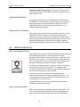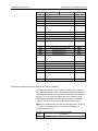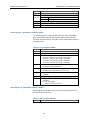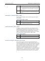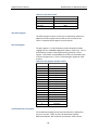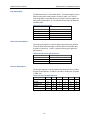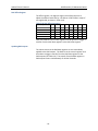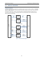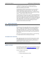
1
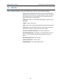
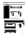
AXM-A75 Multifunction I/O Mezzanine Module USER’S MANUAL ACROMAG INCORPORATED 30765 South Wixom Road P.O. BOX 437 Wixom, MI 48393-7037 U.S.A. Tel: (248) 624-0310 Fax: (248) 624-9234 Copyright 2013, Acromag, Inc., Printed in the USA. Data and specifications are subject to change without notice. 8500-927 A13A000 AXM-A75 User’s Manual 1.0 Multifunction I/O Mezzanine Board GENERAL INFORMATION ................................................................................................................. 5 KEY FEATURES .................................................................................................................................. 5 ENGINEERING DESIGN KIT ............................................................................................................... 6 BOARD CONTROL SOFTWARE .......................................................................................................... 6 2.0 PREPARATION FOR USE ................................................................................................................... 6 UNPACKING AND INSPECTION ......................................................................................................... 6 CARD CAGE CONSIDERATIONS ......................................................................................................... 6 Front Panel Field I/O Connector J1 .................................................................................................. 8 Analog Inputs: Noise and Grounding Considerations ...................................................................... 9 Non-Isolation Considerations .......................................................................................................... 9 3.0 PROGRAMMING INFORMATION ...................................................................................................... 9 AXM-A75 Memory Map ................................................................................................................... 9 FLASH Data Format ........................................................................................................................ 13 Board Status and Reset Register (Read/Write, PCIBar2 + 8000H) ................................................. 14 Control Register - (Read/Write, PCIBar2 + 8100H) ........................................................................ 15 Status Register 0 - (Read/Write, PCIBar2 + 8104H) ....................................................................... 15 Status Register 1 - (Read/Write, PCIBar2 + 8108H) ....................................................................... 16 Digital I/O (Read/Write, PCIBar2 + 810CH) .................................................................................... 16 Conversion Timer Register - (Read/Write, PCIBar2 + 8110H)........................................................ 16 FLASH Data Register - (Read/Write, PCIBar2 + 8114H) ................................................................. 17 Digital I/O Direction Register - (Read/Write, PCIBar2 + 8118H) .................................................... 17 ADC Channels ................................................................................................................................. 17 ADC Data Format ........................................................................................................................... 17 ADC Offset Register........................................................................................................................ 18 ADC Gain Register .......................................................................................................................... 18 Uncalibrated ADC Performance ..................................................................................................... 18 Analog Input Channel Calibration Procedure ................................................................................ 19 DAC Channels ................................................................................................................................. 19 DAC Data Register .......................................................................................................................... 21 DAC Coarse Gain Register .............................................................................................................. 21 DAC Fine Gain Register .................................................................................................................. 21 DAC Offset Register........................................................................................................................ 22 Updating DAC outputs ................................................................................................................... 22 4.0 THEORY OF OPERATION ................................................................................................................. 23 Field I/O Connections..................................................................................................................... 23 -2- AXM-A75 User’s Manual Multifunction I/O Mezzanine Board Digital I/O ....................................................................................................................................... 24 Analog Outputs .............................................................................................................................. 24 Analog Inputs ................................................................................................................................. 24 5.0 SERVICE AND REPAIR ..................................................................................................................... 25 SERVICE AND REPAIR ASSISTANCE ................................................................................................. 25 PRELIMINARY SERVICE PROCEDURE .............................................................................................. 25 WHERE TO GET HELP ..................................................................................................................... 25 6.0 SPECIFICATIONS ............................................................................................................................. 26 Physical .......................................................................................................................................... 26 Connectors ..................................................................................................................................... 26 Environmental................................................................................................................................ 26 Power Requirements ..................................................................................................................... 27 ANALOG INPUTS............................................................................................................................. 27 Programmable Gain Instrumentation Amplifier ............................................................................ 27 Difference Amplifier....................................................................................................................... 28 Voltage Reference REF3240 ........................................................................................................... 28 Analog to Digital Converter............................................................................................................ 28 ANALOG OUTPUTS ......................................................................................................................... 29 Digital to Analog Converter............................................................................................................ 29 7.0 APPENDIX ....................................................................................................................................... 30 CABLE: MODEL 5028-420 (Ultra SCSI/VHDCI male to SCSI-3 male, Round, Shielded) ................ 30 TERMINATION PANEL: MODEL 5025-288 ...................................................................................... 31 8.0 DRAWINGS ..................................................................................................................................... 32 -3- AXM-A75 User’s Manual Multifunction I/O Mezzanine Board The information contained in this manual is subject to change without notice. Acromag, Inc. makes no warranty of any kind with regard to this material, including, but not limited to, the implied warranties of merchantability and fitness for a particular purpose. Further, Acromag, Inc. assumes no responsibility for any errors that may appear in this manual and makes no commitment to update, or keep current, the information contained in this manual. No part of this manual may be copied or reproduced in any form, without the prior written consent of Acromag, Inc. IMPORTANT SAFETY CONSIDERATIONS It is very important for the user to consider the possible adverse effects of power, wiring, component, sensor, or software failures in designing any type of control or monitoring system. This is especially important where economic property loss or human life is involved. It is important that the user employ satisfactory overall system design. It is agreed between the Buyer and Acromag, that this is the Buyer's responsibility. -4- AXM-A75 User’s Manual 1.0 Multifunction I/O Mezzanine Board GENERAL INFORMATION The AXM-A75 is a high speed analog input/output mezzanine board compatible with Acromag’s line of re-configurable PMC and XMC FPGA modules. The AXM-A75 has 16 differential analog inputs, 8 analog outputs and 16 digital inputs/outputs. KEY FEATURES High Speed Analog Input - sixteen independent 16-bit Analog to Digital Converter (ADC) channels provide simultaneous sampling at a maximum rate of 500 KHz. The digitized output of each ADC is simultaneously input to the Field Programmable Gate Array (FPGA) for data collection and processing. Programmable Input Voltage Range - four gain selections are available that allow a bipolar input voltage range from ± 1.28 Volts to ± 10.24 Volts. Analog Output – eight 16-bit Digital to Analog Converter (DAC) channels provide simultaneous update with a maximum rate of 100 KHz. Programmable Output Voltage Range – three gain selections are available that allow a bipolar output voltage range from ± 10 Volts to ± 10.5263 Volts. Calibration Constants – factory calibration constants used to correct gain and offset errors are stored in on-board FLASH memory. Correction constants are stored for each channel and gain selection combination. Gain and offset correction are supported for both analog input and analog output. General Purpose Digital Input or Output – sixteen general purpose I/O signals are provided. The outputs are pulled high via pull-up resistors. Example Design – the example VHDL design provided in the base board EDK provides the following features: Control of ADC sample rate and gain selection. Gain and offset error correction is applied in FPGA hardware for analog inputs and on-chip for analog outputs. Each ADC channel includes a FIFO capable of storing 2050 samples. All enabled ADC channels are sampled simultaneously. ADC sample rate can range from 1/34 Hz to 500 KHz. Control of DAC gain selection. -5- AXM-A75 User’s Manual Multifunction I/O Mezzanine Board Analog Input FIFO Status Interrupts – Interrupts can be generated when an input channel’s FIFO half full condition is reached or when a FIFO overflow occurs. ENGINEERING DESIGN KIT Acromag does not provide an engineering design kit specifically for the AXM-A75 module. However, an example design is included in the Engineering Design Kit of the PMC/XMC base board. Refer to the PMC/XMC base board’s manual for further information on the available Engineering Design Kit. BOARD CONTROL SOFTWARE Acromag does not provide board control software specifically for the AXM-A75 series board. However, the AXM-A75 module can be accessed via the control software for the base PMC or XMC module. These products (sold separately) facilitate the product interface in the following operating systems: Windows™DLL, VxWorks, and Linux. Refer to the PMC/XMC base board’s manual for further information. 2.0 PREPARATION FOR USE UNPACKING AND INSPECTION Upon receipt of this product, inspect the shipping carton for evidence of mishandling during transit. If the shipping carton is badly damaged or water stained, request that the carrier's agent be present when the carton is opened. If the carrier's agent is absent when the carton is opened and the contents of the carton are damaged, keep the carton and packing material for the agent's inspection. For repairs to a product damaged in shipment, refer to the Acromag Service Policy to obtain return instructions. It is suggested that salvageable shipping cartons and packing material be saved for future use in the event the product must be shipped. This board is physically protected with packing material and electrically protected with an anti static bag during shipment. It is recommended that the board be visually inspected for evidence of mishandling prior to applying power. The board utilizes static sensitive components and should only be handled at a static-safe workstation. CARD CAGE CONSIDERATIONS Refer to the specifications for loading and power requirements. Be sure that the system power supplies are able to accommodate the power requirements of the carrier board, plus the installed PMC or -6- AXM-A75 User’s Manual Multifunction I/O Mezzanine Board XMC modules, plus the AXM-A75 within the voltage tolerances specified. IMPORTANT: Adequate air circulation must be provided to prevent a temperature rise above the maximum operating temperature. The lack of air circulation within the computer chassis is a cause for some concern. Most, if not all, computer chassis do not provide a fan for cooling of add-in boards. The dense packing of the mezzanine modules to the carrier board alone results in elevated module and carrier board temperatures, and the restricted air flow within the chassis aggravates this problem. Adequate air circulation must be provided to prevent a temperature rise above the maximum operating temperature and to prolong the life of the electronics. If the installation is in an industrial environment and the board is exposed to environmental air, careful consideration should be given to air-filtering. -7- AXM-A75 User’s Manual Multifunction I/O Mezzanine Board Front Panel Field I/O Connector J1 The AXM-A75 front panel field I/O connector (J1) is a 68 pin VHDCI receptacle. A cable assembly and termination panel (or user defined terminations) can be quickly mated to the field I/O connector. The pin assignment for this connector is shown in Table 2-1. Table 2-1 J1 Pin Assignment Pin Description GND DIO1 DIO3 DIO5 DIO7 DIO8 DIO10 DIO12 DIO14 GND GND GND GND GND GND GND GND GND VIN16VIN15VIN14VIN13VIN12VIN11VIN10VIN9VIN8VIN7VIN6VIN5VIN4VIN3VIN2VIN1- Number 1 2 3 4 5 6 7 8 9 10 11 12 13 14 15 16 17 18 19 20 21 22 23 24 25 26 27 28 29 30 31 32 33 34 Pin Description DIO0 DIO2 DIO4 DIO6 GND DIO9 DIO11 DIO13 DIO15 VOUT1 VOUT2 VOUT3 VOUT4 VOUT5 VOUT6 VOUT7 VOUT8 GND VIN16+ VIN15+ VIN14+ VIN13+ VIN12+ VIN11+ VIN10+ VIN9+ VIN8+ VIN7+ VIN6+ VIN5+ VIN4+ VIN3+ VIN2+ VIN1+ Number 35 36 37 38 39 40 41 42 43 44 45 46 47 48 49 50 51 52 53 54 55 56 57 58 59 60 61 62 63 64 65 66 67 68 The sixteen differential analog input channels are labeled VINx- and VINx+ where x is the channel number 1 to 16. Analog outputs are labeled VOUTx where x is the channel number 1 to 8. Digital input / output signals are labeled DIOx where x is bit 0 to 15. Signal returns are labeled GND. -8- AXM-A75 User’s Manual Multifunction I/O Mezzanine Board Analog Inputs: Noise and Grounding Considerations Differential inputs require two leads (+ and -) per channel, and provide rejection of common mode voltages. This allows the desired signal to be accurately measured. However, the signal being measured cannot be floating. It must be referenced to analog common on the AXM module and be within the normal input voltage range. Shielded cable of the shortest length possible is strongly recommended. Non-Isolation Considerations The board is non-isolated, since there is electrical continuity between the logic and field I/O grounds. As such, the field I/O connections are not isolated from the system. Care should be taken in designing installations without isolation to avoid noise pickup and ground loops caused by multiple ground connections. 3.0 PROGRAMMING INFORMATION This Section provides the specific information necessary to program and operate the mezzanine board. This mezzanine board is intended only for use on specific Acromag PMC/XMC FPGA modules. As such only a small portion of I/O memory space is currently reserved for operation of the mezzanine board. The remaining memory space is defined in the base board’s User’s Manual. AXM-A75 Memory Map The AXM-A75 specific memory space address map for the board is shown in Table 3-1. Note that the base address from the base PMC/XMC module in memory space must be added to the addresses shown to properly access the board registers. Register accesses as 32, 16, and 8-bits in memory space are permitted unless otherwise indicated. A detailed description of each of the registers follows after Table 3-1. Table 3-1 Memory Map PCIBar2 + (Hex) 0003 ↓ 7FFF 8003 8007 ↓ 80FF 8103 D31 D16 D15 D00 Reserved for base PMC/XMC Module Board Status Register and Software Reset Reserved for base PMC/XMC Module Control Register -9- PCIBar2 + (Hex) 0000 ↓ 7FFC 8000 8004 ↓ 80FC 8100 AXM-A75 User’s Manual Multifunction I/O Mezzanine Board PCIBar2 + (Hex) 8107 810B 810F 8113 8117 D31 811B 811F ↓ 81FF 8203 8207 820B 820F 8213 8217 821B 821F 8223 8227 822B 822F 8233 8237 823B 823F 8243 8247 824B 824F 8253 8257 825B 825F 8263 8267 826B 826F 8273 8277 827B 827F 8283 8287 828B 828F 8293 D16 D15 D00 Status Register 0 Status Register 1 Digital I/O Conversion Timer FLASH data Digital I/O Direction unused ADC 1 data ADC1 gain correction ADC 1 offset unused ADC 2 data ADC 2 gain correction ADC 2 offset unused ADC 3 data ADC 3 gain correction ADC 3 offset unused ADC 4 data ADC 4 gain correction ADC 4 offset unused ADC 5 data ADC 5 gain correction ADC 5 offset unused ADC 6 data ADC 6 gain correction ADC 6 offset unused ADC 7 data ADC 7 gain correction ADC 7 offset unused ADC 8 data ADC 8 gain correction ADC 8 offset unused ADC 9 data ADC 9 gain correction ADC 9 offset unused ADC 10 data - 10 - PCIBar2 + (Hex) 8104 8108 810C 8110 8114 8118 811C ↓ 81FC 8200 8204 8208 820C 8210 8214 8218 821C 8220 8224 8228 822C 8230 8234 8238 823C 8240 8244 8248 824C 8250 8254 8258 825C 8260 8264 8268 826C 8270 8274 8278 827C 8280 8284 8288 828C 8290 AXM-A75 User’s Manual Multifunction I/O Mezzanine Board PCIBar2 + (Hex) 8297 829B 829F 82A3 82A7 82AB 82AF 82B3 82B7 82BB 82BF 82C3 82C7 82CB 82CF 82D3 82D7 82DB 82DF 82E3 82E7 82EB 82EF 82F3 82F7 82FB 82FF 8303 D31 8307 830B 830F 8313 8317 831B 831F 8323 8327 - 11 - D16 D15 D00 ADC 10 gain correction ADC 10 offset unused ADC 11 data ADC 11 gain correction ADC 11 offset unused ADC 12 data ADC 12gain correction ADC 12 offset unused ADC 13 data ADC 13 gain correction ADC 13 offset unused ADC 14 data ADC 14 gain correction ADC 14 offset unused ADC 15 data ADC 15 gain correction ADC 15 offset unused ADC 16 data ADC 16 gain correction ADC 16 offset unused DAC 1 data DAC 1 coarse gain DAC 1 fine gain DAC 1 offset DAC 2 data DAC 2 coarse gain DAC 2 fine gain DAC 2 offset DAC 3 data DAC 3 coarse gain PCIBar2 + (Hex) 8294 8298 829C 82A0 82A4 82A8 82AC 82B0 82B4 82B8 82BC 82C0 82C4 82C8 82CC 82D0 82D4 82D8 82DC 82E0 82E4 82E8 82EC 82F0 82F4 82F8 82FC 8300 8304 8308 830C 8310 8314 8318 831C 8320 8324 AXM-A75 User’s Manual Multifunction I/O Mezzanine Board PCIBar2 + (Hex) D31 832B 832F 8333 8337 833B 833F 8343 8347 834B 834F 8353 8357 835B 835F 8363 8367 836B 836F 8373 8377 837B 837F 8383 ↓ 1FFFFF D16 D15 D00 DAC 3 fine gain DAC 3 offset DAC 4 data DAC 4 coarse gain DAC 4 fine gain DAC 4 offset DAC 5 data DAC 5 coarse gain DAC 5 fine gain DAC 5 offset DAC 6 data DAC 6coarse gain DAC 6 fine gain DAC 6 offset DAC 7 data DAC 7 coarse gain DAC 7 fine gain DAC 7 offset DAC 8 data register DAC 8 coarse gain DAC 8 fine gain DAC 8 offset Reserved for base PMC Module - 12 - PCIBar2 + (Hex) 8328 832C 8330 8334 8338 833C 8340 8344 8348 834C 8350 8354 8358 835C 8360 8364 8368 836C 8370 8374 8378 837C 8380 ↓ 1FFFFC AXM-A75 User’s Manual Multifunction I/O Mezzanine Board FLASH Data Format Factory calibration constants are stored in FLASH memory. The FLASH memory device is a Numonyx M25P10. Error! Reference source not ound. shows the memory map of the FLASH contents. All numeric constants are 32 bit values stored in little endian byte order. Table 3-2 FLASH Memory Map Addr 0007 000B 000F 0013 0047 004B 004F 0053 0087 008B 008F 0093 00C7 00CB 00CF 00D3 0107 010B 010F 0113 0147 014B 014F 0153 D31 D16 D15 D00 FLASH ID = “AXM-A75” (null terminated character string) 10.24 Volt Range Channel 1 Offset 10.24 Volt Range Channel 2 Offset 10.24 Volt Range Channel 3 Offset . . . 10.24 Volt Range Channel 16 Offset 10.24 Volt Range Channel 1 Gain 10.24 Volt Range Channel 2 Gain 10.24 Volt Range Channel 3 Gain . . . 10.24 Volt Range Channel 16 Gain 5.12 Volt Range Channel 1 Offset 5.12 Volt Range Channel 2 Offset 5.12 Volt Range Channel 3 Offset . . . 5.12 Volt Range Channel 16 Offset 5.12 Volt Range Channel 1 Gain 5.12 Volt Range Channel 2 Gain 5.12 Volt Range Channel 3 Gain . . . 5.12 Volt Range Channel 16 Gain 2.56 Volt Range Channel 1 Offset 2.56 Volt Range Channel 2 Offset 2.56 Volt Range Channel 3 Offset . . . 2.56 Volt Range Channel 16 Offset 2.56 Volt Range Channel 1 Gain 2.56 Volt Range Channel 2 Gain 2.56 Volt Range Channel 3 Gain . . - 13 - Addr 0000 0008 000C 0010 0044 0048 004C 0050 0084 0088 008C 0090 00C4 00C8 00CC 00D0 0104 0108 010C 0110 0144 0148 014C 0150 AXM-A75 User’s Manual Multifunction I/O Mezzanine Board Addr 0187 018B 018F 0193 01C7 01CB 01CF 01D3 0207 020B 020F 0213 0227 0247 024B 024F 0253 0267 D31 D16 D15 D00 . Channel 16 Gain Channel 1 Offset Channel 2 Offset Channel 3 Offset . . . 1.28 Volt Range Channel 16 Offset 1.28 Volt Range Channel 1 Gain 1.28 Volt Range Channel 2 Gain 1.28 Volt Range Channel 3 Gain . . . 1.28 Volt Range Channel 16 Gain DAC Offset Channel 1 DAC Offset Channel 2 DAC Offset Channel 3 . . . DAC Offset Channel 8 Unused DAC Gain Channel 1 DAC Gain Channel 2 DAC Gain Channel 3 . . . DAC Gain Channel 8 2.56 Volt Range 1.28 Volt Range 1.28 Volt Range 1.28 Volt Range Addr 0184 0188 018C 0190 01C4 01C8 01CC 01D0 0204 0208 020C 0210 0224 0228 0248 024C 0250 0264 Board Status and Reset Register (Read/Write, PCIBar2 + 8000H) This read/write register is used to issue a software reset, view and clear pending interrupts, and to identify the attached AXM module. It may also provide other functions that are defined by the base board. Writing a “1” to bit 31 of this register will cause a software reset affecting both the PMC base board and the majority of AXM-A75 registers. Bits 15 to 13 are used for AXM identification code. Read of this register reflects the interrupt pending status. Read of a “1” in bits 1 or 0 indicates that an interrupt is pending for the corresponding interrupt. Table 3-3 Board Status and Reset Register 8000H BIT 31 FUNCTION Software Reset (Write Only) - 14 - AXM-A75 User’s Manual Multifunction I/O Mezzanine Board BIT 30- 16 15 - 13 12 - 2 1 0 FUNCTION Reserved for base board AXM Identification bits (Read Only) AXM-EDK “001” AXM-A75 “011” Reserved for base board FIFO overflow interrupt pending FIFO half full interrupt pending Control Register - (Read/Write, PCIBar2 + 8100H) The control register is used to enable interrupts, control amplifier gain, control the FLASH chip select signal, and start/stop the A/D converter for each channel. See Table 3-4 for a description of each of the register bits. Table 3-4 Control Register 8100H BIT FUNCTION 31 FIFO overflow interrupt enable 30 FIFO half full interrupt enable 29 – 28 Amplifier Gain “00” Gain 1, full scale input range ± 10.24 Volts “01” Gain 2, full scale input range ± 5.12 Volts “10” Gain 4, full scale input range ± 2.56 Volts “11” Gain 8, full scale input range ± 1.28 Volts 27 FLASH Select – This bit is connected directly to the “select” input of the serial FLASH device. 26 LDAC – transfer DAC data from data registers to output registers, all channels (write only, read zero) 25 CLR – clear DAC data registers to 0x00 all channels, (write only, read zero) 24 – 16 unused 15 – 0 Convert channel [16 .. 1]– each channel can be individually controlled 0 – channel stopped 1 – enable continuous conversion Status Register 0 - (Read/Write, PCIBar2 + 8104H) Status Register 0 provides access to the FIFO overflow and half full status bits for each channel. Table 3-5 Status Register 0 8104H BIT FUNCTION - 15 - AXM-A75 User’s Manual Multifunction I/O Mezzanine Board BIT 31- 16 15 - 0 FUNCTION FIFO overflow interrupt pending / clear channel [16 .. 1] A ‘1’ indicates that at least one A/D sample was lost due to an attempted write to a full FIFO. Write a ‘1’ to clear the bit. FIFO half full interrupt pending channel [16 .. 1] A ‘1’ indicates that there are at least 1024 samples in the FIFO. Status Register 1 - (Read/Write, PCIBar2 + 8108H) Status Register 1 provides access to the FIFO empty status bits for each channel. Table 3-6 Status Register 1 8108H BIT FUNCTION 31 – 16 Unused 15 – 0 FIFO empty channel [16 .. 1] A ‘1’ indicates that the FIFO is empty. Digital I/O (Read/Write, PCIBar2 + 810CH) The Digital I/O register provides access to the 16 digital I/O lines. Digital I/O lines are pulled high via a 4.75K Ohm resistor to +5 Volts. The levels of the digital I/O lines are returned upon a read to this address. The appropriate output enable bit must be ‘1’ in the Digital I/O Direction register to enable writing to a digital output. Table 3-7 Digital I/O 810CH BIT 31 - 16 15 - 0 FUNCTION unused Digital I/O signals [15 .. 0] Conversion Timer Register - (Read/Write, PCIBar2 + 8110H) This read/write register controls the sample period of all A/D converters. Sample period = count * ADC Clock Period. Set count to zero to allow A/D converters to sample at their maximum rate of 500 KHz. For sample rates less than 500 KHz, enter a count > 2 µS/ADC Clock Period. This register must be written using a 32 bit write command. The minimum sample period is 2 µS. The maximum sample period is (232 - 1) * ADC Clock Period. The ADC Clock Period is 10.101 nS for host boards based on Xilinx Virtex 4 FPGA’s. The ADC Clock Period is 8 nS for host boards based on Virtex 5 or Spartan 6. - 16 - AXM-A75 User’s Manual Multifunction I/O Mezzanine Board Table 3-8 Conversion Timer 8110H BIT 31 – 0 FUNCTION Sample Period = register value * ADC Clock Period FLASH Data Register - (Read/Write, PCIBar2 + 8114H) A byte write to this address triggers a write/read serial transfer to/from the serial FLASH device. A byte read from this address returns the data read from a previous write/read serial transfer. WARNING: Factory calibration data is stored in FLASH. Writing to FLASH could result in loss of factory calibration data. See Error! eference source not found.. Table 3-9 FLASH Data Register 8114H BIT 31 - 8 7-0 FUNCTION unused FLASH data Digital I/O Direction Register - (Read/Write, PCIBar2 + 8118H) The Digital I/O Direction provides an output enable for each of the 16 digital I/O lines. Write a ‘1’ to a bit to enable the output. Table 3-10 Digital I/O 8118CH BIT 31 - 16 15 - 0 FUNCTION unused Digital I/O Direction [15 .. 0] 0 – input 1 – output ADC Channels There are three registers associated with each of the sixteen ADC channels: data, gain correction, and offset correction. The data register is a 16-bit read only register. Reading this register will retrieve the oldest value from the FIFO associated with that channel. Each of the ADC channels will apply a gain and offset correction to each sample prior to writing the result to a FIFO. The addition and multiplication operations are done in FPGA hardware using one of the FPGA’s DSP blocks for each channel. The gain and offset registers are set to one and zero respectively upon reset to pass uncorrected ADC values to the FIFOs. Typical start-up operation would include reading factory calibration constants from AXM-A75 on-board FLASH memory and writing the appropriate correction values for the currently selected full scale range to the gain and offset registers for each channel. ADC Data Format The output from the ADC is offset binary format as shown in Table 3-11. The full scale range (±10.24, ±5.12, ±2.56, ±1.28) is controlled by the gain selection in the control register. See Table 3-4. - 17 - AXM-A75 User’s Manual Multifunction I/O Mezzanine Board Table 3-11 ADC Data Format DESCRIPTION DIGITAL OUTPUT + Full Scale Midscale (zero) 1 LSB Below Midscale - Full Scale FFFF 8000 7FFF 0000 ADC Offset Register The offset register contains a 16 bit two’s complement value that is added to the value output from the ADC to correct offset errors. There is a separate offset register for each channel. ADC Gain Register The gain register is a 17 bit fixed point positive fractional number ranging from 0 to 1.999984 weighted as shown in Table 3-12. The 17 bit fixed point number is least significant bit justified in a 32 bit register. This number is multiplied by the offset corrected ADC value to correct for gain errors. There is a separate gain register for each channel. Table 3-12 Gain Register Number Format BIT Binary Fixed Point 31 - 17 16 15 14 13 12 11 10 9 8 7 6 5 4 3 2 1 0 (unused, read as 0) 1 1/2 1/4 1/8 1/16 1/32 1/64 1/128 1/256 1/1024 1/2048 1/4096 1/8192 1/16536 1/32768 1/65536 1/131072 Uncalibrated ADC Performance The uncalibrated analog input channel performance is affected by four error sources. These are the instrumentation amplifier, difference amplifier, ADC reference and the ADC. Each of these - 18 - AXM-A75 User’s Manual Multifunction I/O Mezzanine Board devices can contribute to the offset and gain error of the system. These errors can be corrected by calibration. Analog Input Channel Calibration Procedure Accurate calibration of the analog input channel digitized values can be accomplished by applying external precision calibration voltages. The calibration voltages are used to find two points that determine the straight line characteristic of the analog channel. Factory calibration constants are calculated using the following equations. ‖ ‖ ‖ ‖ The values calculated for OffsetCorrection and GainCorrection are stored in FLASH memory for each gain selection for each ADC channel. The values are then used in the following equation to correct each input sample for offset and gain errors. ( ) Note: The average of many ADC values (e.g. 2048) should be used when calculating new correction coefficients to reduce the measurement uncertainty. DAC Channels There are four registers associated with each of the eight ADC channels: data, coarse gain correction, fine gain correction and offset correction. The data register is a 16-bit write/read register. Reading this register will retrieve the last value that was loaded into the DAC - 19 - AXM-A75 User’s Manual Multifunction I/O Mezzanine Board register for that channel. Each of the D/A channels will apply a gain and offset correction to each output word. The addition and multiplication operations are done in each DAC device. The gain and offset registers are set to one and zero respectively upon reset to pass uncorrected DAC values to the outputs. Typical start-up operation would include reading factory calibration constants from AXM-A75 on-board FLASH memory and writing the appropriate correction values for the currently selected full scale range to the coarse gain, fine gain and offset registers for each channel. - 20 - AXM-A75 User’s Manual Multifunction I/O Mezzanine Board DAC Data Register The DAC data format is 16 bit offset binary. The ideal output from the DAC for some select output codes is shown in Table 3-13. The full scale range (FSR) is controlled by the coarse gain selection register for each channel (See Table 3-4). The FSR choices are ±10, ±10.2564 and ±10.5263 Volts. Table 3-13 DAC Data Format Volts DIGITAL OUTPUT +FSR * 32767/32768 +FSR * 1/32767 Midscale (zero) -FSR * 1/32767 -FSR * 32767/32768 FFFF 8001 8000 7FFF 0000 DAC Coarse Gain Register The coarse gain register is a two bit register that allows the selection of one of three Full Scale Ranges: ±10, ±10.2564 and ±10.5263 Volts as shown in Table 3-14. There is a separate coarse gain register for each channel. Table 3-14 DAC Coarse Gain Selections FSR Volts Register Value ±10 ±10.2564 ±10.5263 0 1 2 DAC Fine Gain Register The fine gain register is a six bit register that allows the user to adjust the gain of each DAC by −32 LSBs to +31 LSBs in 1 LSB steps, as shown in Table 3-15. Table 3-15 DAC Fine Gain Selections Gain Adjustment +31 LSBs +30 LSBs No adjustment -30 LSBs -31 LSBs - 21 - FG5 FG4 FG3 FG2 FG1 FG0 0 0 0 1 1 1 1 0 0 0 1 1 0 0 0 1 1 0 0 0 1 1 0 0 0 1 0 0 1 0 AXM-A75 User’s Manual Multifunction I/O Mezzanine Board DAC Offset Register The offset register is an eight bit register that allows the user to adjust the offset of each DAC by −16 LSBs to +15.875 LSBs in steps of one-eighth LSB, as shown in Table 3-16. Table 3-16 DAC Offset Correction Gain Adjustment +15.875 LSBs +15.75 LSBs No adjustment -15.875 LSBs -16 LSBs OF7 OF6 OF5 OF4 OF3 OF2 OF1 OF0 0 0 0 1 1 1 1 0 0 0 1 1 0 0 0 1 1 0 0 0 1 1 0 0 0 1 1 0 0 0 1 1 0 0 0 1 0 0 1 0 Note: the LDAC bit in the control register must be written to trigger a transfer from the DAC data registers to the DAC offset register. Updating DAC outputs The values written to the DAC data registers are not immediately applied to the DAC outputs. The LDAC bit in the control register must be written to trigger a transfer from the DAC data registers to the DAC outputs (see Table 3-4). The transfer from the data register to DAC outputs occurs simultaneously for all DAC channels. - 22 - AXM-A75 User’s Manual 4.0 Multifunction I/O Mezzanine Board THEORY OF OPERATION Field I/O Connections The field I/O interface to the AXM-A75 is provided through connector P1 (refer to Table 2-1). Field I/O signals are NON-ISOLATED. This means that the field return and logic common have a direct electrical connection to each other. As such, care must be taken to avoid ground loops (see Section 2.0 for connection recommendations). Ignoring this effect may cause operation errors, and with extreme abuse, possible circuit damage. 16 16 bit Digital I/O 16 C CHEESE HEAD SCREW M2.5 x 4 AXM MODULE FIELD noew CONVERT1 SCLK1 A2D_DATA1 16 bit A/D AIN1 A ASSEMBLY PROCEDURE COMPONENT SIDE OF MODULE JACK SCREW (2 PLACES) 1. LOOSEN JACK SCREWS, ITEM A. MEZZANINE CONNECTOR 2. CONNECT THE METAL STANDOFFS TO PM WITH CHEESE HEAD SCREWS 2.5 x 4, ITE DO NOT TIGHTEN. CMC BEZEL SHOWN INSTALLED 16 channels FIELD I/O P1 CONVERT16 AIN16 16 bit A/D SCL A2D_DATA16 3. CAREFULLY ALIGN THE CONNECTORS ON AXM MODULE. PUSH TOGETHER (D). STAC TO FPGA D 4. INSTALL CHEESE HEAD SCREWS, ITEM C, 5. TIGHTEN JACK SCREWS, ITEM A, (2 PLACE 6. TIGHTEN CHEESE HEAD SCREWS, ITEMS B PMC/XMC MODULE AOUT1 AOUT2 AOUT3 AOUT4 AOUT5 AOUT6 AOUT7 AOUT8 LDAC1 METAL SCK1STANDOFF 16 bit Quad D/A (2 PLACES) D2A_DATA1 PMC CONNECTOR COMPONENT SIDE OF MODULE LDAC2 16 bit SCK2 Quad B CHEESE HEAD SCREW M2.5 x 4 D2A_DATA2 D/A AXM-A75 MECHANICAL ASSEMBLY WITH CMC BEZEL INSTALLED Figure 1 AXM-A75 Block Diagram - 23 - 450 AXM-A75 User’s Manual Multifunction I/O Mezzanine Board Digital I/O A block diagram of a single digital I/O channel is shown in Figure 2 Digital I/O. This structure is replicated 16 times on the AXM-A75. The signal DIG_OUT_STROBE is activated upon a write to the Digital I/O register. The level of DIG_IO_n is returned upon a read of the Digital I/O register. The signal DIG_OUT_DIR_STROBE is activated upon a write to the Digital I/O Direction Register. When the DIG_OUT_DIR_n signal is logic high the contents of the DIG_OUT_n flip-flop will be driven onto the DIG_IO_n signal. The level translator is a NXP GTL2010. Figure 2 Digital I/O Analog Outputs Two Analog Devices AD5764R quad bipolar voltage output DACs are used to provide the eight analog output channels. Each DAC uses its own on-chip reference as its reference source. Although each DAC has separate clock, sync, load and serial I/O signals connected to the FPGA, the firmware as delivered with the EDK provides access to only a single quad DAC at a time. The CLR, BIN2SCOMP and RESET signals are common to both DACs. Analog Inputs Each of the analog input channels consists of a differential low pass filter followed by an instrumentation amplifier, a difference amplifier and an ADC. - 24 - AXM-A75 User’s Manual Multifunction I/O Mezzanine Board The differential low pass RC filter is intended to reduce RF interference. The 3db cutoff frequency of the filter is 421 kHz differential, 8.84 MHz common mode. An Analog Devices AD8251 Programmable Gain (Instrumentation) Amplifier (PGA) takes as input the channel’s + and - inputs and outputs a single ended voltage proportional to it. The gain can be 1, 2, 4, or 8 and is selected through the gain selection bits in the control register. The gain selection affects all channels. The output from the PGA is input to a Texas Instruments INA159 level translation difference amplifier that divides its input voltage by 5 and level shifts the output by one half of the 4.096 reference voltage. The output from the difference amplifier drives an Analog Devices AD7686 16 bit, 500 kSPS ADC. Each of the ADCs has separate clock, convert and serial data connections to the FPGA allowing synchronous acquisition and simultaneous data transfer. 5.0 SERVICE AND REPAIR SERVICE AND REPAIR ASSISTANCE Surface-Mounted Technology (SMT) boards are generally difficult to repair. It is highly recommended that a non-functioning board be returned to Acromag for repair. The board can be damaged unless special SMT repair and service tools are used. Further, Acromag has automated test equipment that thoroughly checks the performance of each board. Please refer to Acromag's Service Policy Bulletin or contact Acromag for complete details on how to obtain parts and repair. PRELIMINARY SERVICE PROCEDURE Before beginning repair, be sure that all of the procedures in section 2.0 PREPARATION FOR USE have been followed. Replacement of a suspected faulty unit with one that is known to work correctly is a good technique to isolate a faulty board. CAUTION: POWER MUST BE TURNED OFF BEFORE REMOVING OR INSERTING BOARDS WHERE TO GET HELP If you continue to have problems, your next step should be to visit the Acromag worldwide web site at http://www.acromag.com. Our web site contains the most up-to-date product and software information. Go to the “Support” tab to access: Application Notes Frequently Asked Questions (FAQ’s) - 25 - AXM-A75 User’s Manual Multifunction I/O Mezzanine Board Product Knowledge Base Tutorials Software Updates/Drivers An email question can also be submitted from within the Knowledge Base or directly from the “Contact Us” tab. Acromag’s application engineers can also be contacted directly for technical assistance via telephone or FAX through the numbers listed below. When needed, complete repair services are also available. Phone: 248-295-0310 Fax: 248-624-9234 Email: [email protected] 6.0 SPECIFICATIONS Physical Physical Configuration .................. Single AXM Module Stacking Height ............................. 5 mm Length ........................................... 38.5 mm (1.516 inches) Width ............................................ 73.75 mm (2.904 inches) Board Thickness ............................ 1.59 mm (0.062 inches) Connectors P1 (FPGA Interface) ....................... 162-pin receptacle, 5 mm stack height, high speed terminal strip (Samtec QTS-075-01-L-D-A-K) J1 (Field I/O) .................................. 68-pin VHDCI receptacle (Amphenol HE11-RDA-101-3-C) Environmental Operating Temperature ................ 0 to +70C Relative Humidity .......................... 5-95% non-condensing Storage Temperature .................... -55C to +150C Non-Isolated.................................. Logic and field commons have a direct electrical connection Radiated Field Immunity ............... Designed to comply with IEC61000-4-3 class A Surge Immunity ............................. Not required for signal I/O per European Norm EN61000-6-1 Electric Fast Transient Immunity Designed to comply with IEC61000-4-4 class A Radiated Emissions ....................... Designed to comply with CISPR 16-2-3 class A Electrostatic Discharge ................. Designed to comply with IEC6100-4-2 Level 2 Conducted Radio Frequency Interference Designed to comply with IEC6100-4-6 class A - 26 - AXM-A75 User’s Manual Multifunction I/O Mezzanine Board Power Requirements +3.3 Volts (5%) ............................ 39 mA typical 50 mA maximum +5 Volts (5%) ............................... 54 mA typical 65 mA maximum +12V (5%) .................................... 103 mA typical 115 mA maximum -12V (5%)..................................... 92 mA typical 115 mA maximum ANALOG INPUTS Device............................................ ADI AD7686 Input Channels .............................. 16 differential Input Signal Type........................... Voltage (Non-isolated) Input Ranges: ................................ ±10.24, ±5.12, ±2.56 and ±1.28 V Input Overvoltage Protection ....... ±31 V with power on ±19 V with power off Input Resistance ............................ 5.300 G, typical differential Input Bias Current ......................... 5 nA typical 40 nA maximum Common Mode Rejection Ratio ... 98 dB typical (60 Hz) Input Channel to Input Channel Rejection Ratio1 41 dB typical (100 kHz) Output Channel to Input Channel Rejection Ratio2 85 dB typical (1 kHz) Accuracy ........................................ Gain % Full Scale @ 25°C % Full Scale 0 – 70°C 1 0.011 0.026 2 0.013 0.029 4 0.015 0.033 8 0.018 0.040 Programmable Gain Instrumentation Amplifier Device............................................ ADI AD8251 PGA Linearity Error........................ 0.005 maximum (3.27 LSB) Offset Error RTI3 ............................ 1.0 mV typical, 2.5 mV maximum Offset vs. Temperature ................. (0.6 + 1.5/G) µV/°C typical (G=1,2,4,8) (1.2 + 5/G) µV/°C maximum Gain Error (all gains)3 .................... 0.01 typical, 0.1 maximum 1 Input channel to input channel rejection ratio was measured with a 100 KHz 1V pk-pk sine wave input on an adjacent channel. 2 The output channel to input channel rejection ratio was measured with all output channels driving a 10k ohm load outputting a 1 kHz 20 V pk-pk sine wave. Load resistors were located on a termination panel connected to a 2 meter cable. - 27 - AXM-A75 User’s Manual Multifunction I/O Mezzanine Board Gain vs. Temperature.................... 3 ppm/°C typical 10 pm/°C maximum Difference Amplifier Device............................................ TI INA159 Gain Error ...................................... ±0.005% typical ±0.024% maximum Gain Error vs. Temperature .......... ±1 ppm/°C typical Offset Error ................................... ±100 µV typical ±500 µV maximum Offset Voltage vs. Temperature .... ±1.5 µV/°C typical Reference Divider Accuracy .......... ±0.002% typical ±0.024% maximum Voltage Reference REF3240 Device............................................ TI REF3240 Accuracy ........................................ 0.01% typical ±0.2% maximum Output Voltage Temperature Drift 4 ppm/°C typical 7 ppm/°C maximum Thermal Hysteresis4 ...................... 100 ppm first cycle 25 ppm additional cycles Noise ............................................. 78 µV RMS typical Analog to Digital Converter ADC................................................ ADI AD7686 A/D Resolution .............................. 16-bits Data Format .................................. straight binary No Missing Codes .......................... no missing codes 15-bits A/D Integral Linearity Error ........... 0.6 LSB typical 2 LSB maximum Offset Error ................................... 0.1 mV typical 10 V range 1.6 mV maximum Gain Error Temperature Drift ....... 0.3 ppm/°C typical Offset Temperature Drift .............. 0.3 ppm/°C typical Full Scale Error .............................. 0.5 maximum A/D Conversion Time .................... 2 S maximum Conversion Rate ............................ 500 kHz maximum Input Noise .................................... 2 LSB rms typical 3 Software calibration eliminates these error components Acromag does not temperature cycle this product before shipping to customers. If the product is operated at the extremes of its temperature range, the voltage reference could drift by the amount specified for first cycle. 4 - 28 - AXM-A75 User’s Manual Multifunction I/O Mezzanine Board ANALOG OUTPUTS Digital to Analog Converter Device............................................ ADI AD5764RB Resolution ..................................... 16 bits Output Ranges .............................. ±10, ±10.2564, and ±10.5263 V Settling Time ................................. 8 µS typical full-scale step to ±1 LSB 10 µS maximum Slew Rate....................................... 5 V/µS typical Integral Nonlinearity ..................... ±2 LSB maximum Differential Nonlinearity ............... ±1 LSB maximum Bipolar Zero Error.......................... ±2 mV maximum Internal Reference ........................ 4.995 V minimum 5.005 V maximum Short Circuit Current ..................... 10 mA typical Load Current ................................. ±1 mA maximum for specified performance Capacitive Load Stability ............... 200 pF maximum with RLOAD=∞ 1000 pF maximum with RLOAD=10K Ω DC Output Impedance .................. 0.3 Ω maximum Gain Drift ....................................... ±2 ppm full scale range/°C Bipolar Zero Drift .......................... ±2 ppm full scale range/°C Accuracy ........................................ 0.015 % full scale @ 25°C 0.029 % full scale @ 0 – 70°C - 29 - AXM-A75 User’s Manual 7.0 Multifunction I/O Mezzanine Board APPENDIX CABLE: MODEL 5028-420 (Ultra SCSI/VHDCI male to SCSI-3 male, Round, Shielded) Type: Round shielded cable, 34-wire pairs (Ultra SCSI/VHDCI male and SCSI-3 male connectors). The cable length is 2 meters (6.56 feet). This shielded cable is recommended for all I/O applications (both digital I/O and precision analog I/O). Application: Used to connect Model 5025-288 termination panel to the board. Length: 2 meters (6.56 feet) Cable: 34 wire pairs, 28 AWG, foil/braided shield inside a PVC jacket. Connectors: Ultra SCSI/VHDCI and SCSI-3, 68-pin male connectors with backshell. Keying: The connectors have a “D Shell”. Schematic and Physical Attributes: See Drawing 4502-153. Electrical Specifications: 30 VAC per UL and CSA (SCSI-3 connector spec.’s). 1 Amp maximum at 50% energized (SCSI-3 connector spec.’s). Operating Temperature: -30°C to +80°C. Storage Temperature: -40°C to +85°C. Shipping Weight: 1.0 pound (0.5Kg), packed. - 30 - AXM-A75 User’s Manual Multifunction I/O Mezzanine Board TERMINATION PANEL: MODEL 5025-288 Type: Termination Panel for 68 Pin SCSI-3 Cable Connection Application: To connect field I/O signals to the board. Termination Panel: Acromag Part 4001-066. The 5025-288 termination panel facilitates the connection of up to 68 field I/O signals and connects to the board (connectors only) via a round shielded cable (Model 5028-432). Field signals are accessed via screw terminal strips. The terminal strip markings on the termination panel (1-68) correspond to field I/O (pins 1-68) on the board. Each board has its own unique pin assignments. Refer to the board manual for correct wiring connections to the termination panel. Schematic and Physical Attributes: See Drawing 4501-920. Field Wiring: 68-position terminal blocks with screw clamps. Wire range 12 to 26 AWG. Mounting: Termination panel is snapped on the DIN mounting rail. Printed Circuit Board: Military grade FR-4 epoxy glass circuit board, 0.063 inches thick. Operating Temperature: -40°C to +100°C Storage Temperature: -40°C to +100°C. Shipping Weight: 1.0 pounds (0.5kg) packaged. - 31 - AXM-A75 User’s Manual 8.0 Multifunction I/O Mezzanine Board DRAWINGS P2 P1 68 67 66 65 64 63 62 61 60 59 58 57 56 55 54 53 52 51 50 49 48 47 46 45 44 43 42 41 40 39 38 37 36 35 34 33 32 31 30 29 28 27 26 25 24 23 22 21 20 19 18 17 16 15 14 13 12 11 10 9 8 7 6 5 4 3 2 1 68 67 66 65 64 63 62 61 60 59 58 57 56 55 54 53 52 51 50 49 48 47 46 45 44 43 42 41 40 39 38 37 36 35 34 33 32 31 30 29 28 27 26 25 24 23 22 21 20 19 18 17 16 15 14 13 12 11 10 9 8 7 6 5 4 3 2 1 2 METERS (78.72 INCHES, +4.0 / -0.0 INCHES) P2 P1 TOP VIEW PIN 34 PIN 1 PIN 68 PIN 34 PIN 68 PIN 35 PIN 1 P2 PIN 35 FRONT VIEW P1 MODEL 5028-420 ULTRA SCSI/VHDCI TO SCSI-3 68 PIN CABLE ASSEMBLY, SHIELDED SCHEMATIC 4502-153A J1 1 2 3 4 5 6 7 8 9 10 11 12 13 14 15 16 17 18 19 20 21 22 23 24 25 26 27 28 29 30 31 32 33 34 35 36 37 38 39 40 41 42 43 44 45 46 47 48 49 50 51 52 53 54 55 56 57 58 59 60 61 62 63 64 65 66 67 68 TB1 1 2 3 4 5 6 7 8 9 10 11 12 13 14 15 16 17 18 19 20 21 22 23 24 25 26 27 28 29 30 31 32 33 34 35 36 37 38 39 40 41 42 43 44 45 46 47 48 49 50 51 52 53 54 55 56 57 58 59 60 61 62 63 64 65 66 67 68 MODEL 5025-288 TERMINATION PANEL SCHEMATIC PIN 68 TB2 282-222 J1 1 2 PIN 1 TB2 3.40" (86.36) PLACE MODEL/ SERIAL LABEL HERE. ModeL: Serial: TB1 SIDE VIEW 7.1" (180.34) TOP VIEW 1 2 3 4 5 6 7 8 NOTE: DIMENSIONS ARE IN 9 10 11 12 13 14 15 16 17 18 19 20 21 22 23 24 25 26 27 28 29 30 31 32 33 34 35 36 37 38 39 40 41 42 43 44 45 46 47 48 49 50 51 52 53 54 55 56 57 58 59 60 61 62 63 64 65 66 67 68 2.7" (68.58) INCHES. (MILLIMETERS) TERMINATION MARKINGS 4501-920 FRONT VIEW - 32 - AXM-A75 User’s Manual Multifunction I/O Mezzanine Board - 33 -