1
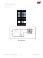
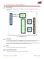
DM35956HR PCIe/104 16-Channel Mechanical Relay Output with 16 Opto-isolated Inputs User’s Manual BDM-610010050 Rev. C RTD Embedded Technologies, Inc. AS9100 and ISO 9001 Certified RTD Embedded Technologies, Inc. 103 Innovation Boulevard State College, PA 16803 USA Telephone: 814-234-8087 Fax: 814-234-5218 www.rtd.com [email protected] [email protected] Revision History Rev A Rev B Rev C Initial Release Corrected some typographical errors. Added ASPM note. Changed to 0 based numbering. Added MTBF. Added wire size specifications for terminal block. Corrected title of Table 5 and 6. Corrected maximum and minimum input voltage specification for opto-isolated inputs. Advanced Analog I/O, Advanced Digital I/O, aAIO, aDIO, a2DIO, Autonomous SmartCal, “Catch the Express”, cpuModule, dspFramework, dspModule, expressMate, ExpressPlatform, HiDANplus, “MIL Value for COTS prices”, multiPort, PlatformBus, and PC/104EZ are trademarks, and “Accessing the Analog World”, dataModule, IDAN, HiDAN, RTD, and the RTD logo are registered trademarks of RTD Embedded Technologies, Inc (formerly Real Time Devices, Inc.). PS/2 is a trademark of International Business Machines Inc. PCI, PCI Express, and PCIe are trademarks of PCI-SIG. PC/104, PC/104-Plus, PCI-104, PCIe/104, PCI/104-Express and 104 are trademarks of the PC/104 Embedded Consortium. All other trademarks appearing in this document are the property of their respective owners. Failure to follow the instructions found in this manual may result in damage to the product described in this manual, or other components of the system. The procedure set forth in this manual shall only be performed by persons qualified to service electronic equipment. Contents and specifications within this manual are given without warranty, and are subject to change without notice. RTD Embedded Technologies, Inc. shall not be liable for errors or omissions in this manual, or for any loss, damage, or injury in connection with the use of this manual. Copyright © 2015 by RTD Embedded Technologies, Inc. All rights reserved. RTD Embedded Technologies, Inc. | www.rtd.com iii DM35956HR User’s Manual Table of Contents 1 Introduction 6 Product Overview........................................................................................................................................................................ 6 Board Features ........................................................................................................................................................................... 6 Ordering Information ................................................................................................................................................................... 7 Contact Information .................................................................................................................................................................... 7 1.4.1 Sales Support 7 1.4.2 Technical Support 7 2 Specifications 8 Operating Conditions .................................................................................................................................................................. 8 Electrical Characteristics ............................................................................................................................................................ 8 3 Board Connection 9 Board Handling Precautions ....................................................................................................................................................... 9 Physical Characteristics .............................................................................................................................................................. 9 Connectors and Jumpers ............................................................................................................................................................ 9 3.3.1 External I/O Connectors 10 CN12: Isolated Input 10 CN10 and CN11: Relay Output with Headers (-H) 11 CN10 and CN11: Relay Output with Screw Terminals (-S) 12 3.3.2 Bus Connectors 12 CN1 (Top) & CN2 (Bottom): PCIe Connector 12 Steps for Installing .................................................................................................................................................................... 13 4 Functional Description 14 Block Diagram........................................................................................................................................................................... 14 PCIe Switch .............................................................................................................................................................................. 14 EPLD......................................................................................................................................................................................... 14 Relays and Opto-Isolators ........................................................................................................................................................ 14 5 Register Address Space 15 Identifying the Board ................................................................................................................................................................. 15 Index and Data Registers ......................................................................................................................................................... 15 5.2.1 GPIOAB_CTRL (Read/Write) 15 5.2.2 GPIOCD_CTRL (Read/Write) 15 5.2.3 SELECT (Read/Write) 15 5.2.4 INDEX_DATA (Read/Write) 16 Accessing the Board Registers ................................................................................................................................................. 16 5.3.1 Reading from a Board Register 16 5.3.2 Writing to a Board Register 17 Board Registers ........................................................................................................................................................................ 18 5.4.1 BUILD_NUM_LS, BUILD_NUM_MS (Read-Only) 18 5.4.2 OPTO_IN (Read-Only) 18 5.4.3 RELAY_CTRL (Read/Write) 18 6 Troubleshooting 19 7 Additional Information 20 PC/104 Specifications ............................................................................................................................................................... 20 PCI and PCI Express Specification .......................................................................................................................................... 20 8 Limited Warranty RTD Embedded Technologies, Inc. | www.rtd.com 21 iv DM35956HR User’s Manual Table of Figures Figure 1: Board Connections .................................................................................................................................................................................... 9 Figure 2: Isolated Input Circuit ................................................................................................................................................................................ 10 Figure 3: Example 104™Stack ............................................................................................................................................................................... 13 Figure 4: DM35956HR Block Diagram ................................................................................................................................................................... 14 Table of Tables Table 1: Ordering Options ........................................................................................................................................................................................ 7 Table 2: Operating Conditions .................................................................................................................................................................................. 8 Table 3: Electrical Characteristics ............................................................................................................................................................................ 8 Table 4: CN12 Isolated Input .................................................................................................................................................................................. 10 Table 5: CN10 Relay Input ..................................................................................................................................................................................... 11 Table 6: CN11 Relay Input ..................................................................................................................................................................................... 11 Table 7: CN10 Relay Input ..................................................................................................................................................................................... 12 Table 8: CN11 Relay Input ..................................................................................................................................................................................... 12 Table 9: Identifying the DM35956HR...................................................................................................................................................................... 15 Table 10: Index and Data Registers ....................................................................................................................................................................... 15 Table 11: Board Registers ...................................................................................................................................................................................... 18 RTD Embedded Technologies, Inc. | www.rtd.com v DM35956HR User’s Manual 1 Introduction Product Overview The DM35956HR provides Opto-Isolated Digital Inputs and Outputs to interface with a variety of devices. The Inputs allow for a broad range of input voltages, and are compatible with 5V systems and 120V systems. The high-current Outputs allow for driving LEDs, relays, and solenoids. The PCIe interface provides compatibility with the latest generation of CPUs, and the PCIe lane repopulation allows for virtually limitless system expansion. Board Features PC/104 form factor PCIe/104 stackable bus structure o PCIe/104 Universal Connector o PCI Express (PCIe) x1 Upstream Interface to CPU o Uses a PCIe x1 link o Repopulates the PCIe bus Broad input voltage range High-current outputs -40 to +85°C Operation Isolated Input o 16 Opto-Isolated digital Inputs o Maximum Input Voltage: Standard Version: 15VDC 24V Version: 30VDC o Reverse-polarity protection o 2500 VAC(RMS) Isolation o Custom settings available Relay Outputs o 16 power relays with Form C contacts o 60 VA switching capacity o Switching current 2 A at 30 VDC 0.5 A at 125 VAC 0.25 A at 250 VAC o Max switching voltage 220 VDC / 250 VAC o Operate and release time 4 milliseconds o 1000 Vrms isolation o Expected life Mechanical (at 180 cpm) 100,000,000 operations Electrical at 2 A, 30 VDC resistive 500,000 operations RTD Embedded Technologies, Inc. | www.rtd.com 6 DM35956HR User’s Manual Ordering Information The DM35956HR is available with the following options: Table 1: Ordering Options Part Number DM35956HR-H DM35956HR-24V-H DM35956HR-S DM35956HR-24V-S IDAN-DM35956HR-D IDAN-DM35956HR-24V-D Description PCIe/104 64-Channel High Density Isolated Digital I/O Module with Headers PCIe/104 64-Channel High Density Isolated Digital I/O Module with Headers for 24V systems PCIe/104 64-Channel High Density Isolated Digital I/O Module with Screw Terminals PCIe/104 64-Channel High Density Isolated Digital I/O Module with Screw Terminals for 24V systems PCIe/104 64-Channel High Density Isolated Digital I/O Module in IDAN enclosure PCIe/104 64-Channel High Density Isolated Digital I/O Module in IDAN enclosure for 24V systems The Intelligent Data Acquisition Node (IDAN™) building block can be used in just about any combination with other IDAN building blocks to create a simple but rugged 104™ stack. This module can also be incorporated in a custom-built RTD HiDAN™ or HiDANplus High Reliability Intelligent Data Acquisition Node. Contact RTD sales for more information on our high reliability systems. Contact Information 1.4.1 SALES SUPPORT For sales inquiries, you can contact RTD Embedded Technologies sales via the following methods: Phone: E-Mail: 1.4.2 1-814-234-8087 [email protected] Monday through Friday, 8:00am to 5:00pm (EST). TECHNICAL SUPPORT If you are having problems with you system, please try the steps in the Troubleshooting section of this manual on page 15. For help with this product, or any other product made by RTD, you can contact RTD Embedded Technologies technical support via the following methods: Phone: E-Mail: 1-814-234-8087 Monday through Friday, 8:00am to 5:00pm (EST). [email protected] RTD Embedded Technologies, Inc. | www.rtd.com 7 DM35956HR User’s Manual 2 Specifications Operating Conditions Table 2: Operating Conditions Symbol Vcc5 Vcc3 Vcc12 Vcc-12 Ta Ts RH Parameter 5V Supply Voltage 3.3V Supply Voltage 12V Supply Voltage -12V Supply Voltage Operating Temperature Storage Temperature Relative Humidity MTBF Mean Time Before Failure Test Condition Non-Condensing Telcordia Issue 2 30°C, Ground benign, controlled Min 4.75 n/a n/a n/a -40 -55 0 Max 5.25 n/a n/a n/a +85 +125 90% Unit V V V V C C % 565,477 Hours Max 3.75 750 Unit W mA Electrical Characteristics Table 3: Electrical Characteristics Symbol P Icc5 Parameter Power Consumption 5V Input Supply Current Test Condition Vcc5 = 5.0V Active PCIe Bus Differential Output Voltage DC Differential TX Impedance Differential Input Voltage DC Differential RX Impedance Electrical Idle Detect Threshold Input Voltage Turn-On Threshold Voltage Isolated Inputs Standard Version 24V Standard Version 24V Min 0.8 95.2 0.175 92.7 61 1.2 116.9 3.3 115.8 173 V Ω V Ω mV -15 -30 1.0 1.0 15 30 2.4 4.5 500 2500 VDC 2.0 0.5 60 220 250 1000 2000 4 A Turn-On Threshold Current Isolation Voltage Nominal switching capacity Relay Outputs 30 VDC, resistive load 125VAC, resistive load Switching Power Switching Voltage Breakdown Voltage (initial) Set time Release time Expected life Operating Speed Terminal Block Wire Size RTD Embedded Technologies, Inc. | www.rtd.com Between open contacts Between contact and coil 20°C, nominal supply voltage Excluding contact bounce 20°C, nominal supply voltage Excluding contact bounce Mechanical, 180 cpm Electrical, 20 cpm 2A @ 30V resistive 1A @ 30V resistive 0.5A @ 125VAC resistive -S version 8 4 1 x 10⁸ VDC μA VAC(RMS) W VDC VAC VRMS VRMS ms ms Cycles 1 x 10⁵ 5 x 10⁵ 1 x 10⁵ 26 20 20 Cpm AWG DM35956HR User’s Manual 3 Board Connection NOTE: It may be necessary to disable PCIe Active State Power Management (ASPM) in the BIOS setup utility for correct operation. This is typically in the “Advanced/PCI Express/Port #” menu. Contact your CPU vendor for details. Board Handling Precautions To prevent damage due to Electrostatic Discharge (ESD), keep your board in its antistatic bag until you are ready to install it into your system. When removing it from the bag, hold the board at the edges, and do not touch the components or connectors. Handle the board in an antistatic environment, and use a grounded workbench for testing and handling of your hardware. Physical Characteristics Weight: Approximately 0.20 lbs. (90 g) Dimensions: 90.17 mm L x 95.89 mm W (3.550 in L x 3.775 in W) Stand-off Height: 0.600 inches (15.240 mm) Connectors and Jumpers CN12: Isolated Input CN10: Relay Output CN11: Relay Output CN1 & CN2: PCIe Connector Figure 1: Board Connections RTD Embedded Technologies, Inc. | www.rtd.com 9 DM35956HR User’s Manual 3.3.1 EXTERNAL I/O CONNECTORS CN12: Isolated Input The Isolated Inputs are on CN12. The pin assignments are shown in the Table below. The Figure below shows the input circuit. Table 4: CN12 Isolated Input Pin Name IN0IN1IN2IN3IN4IN5IN6IN7IN8IN9IN10IN11IN12IN13IN14IN15n.c. # 2 4 6 8 10 12 14 16 18 20 22 24 26 28 30 32 34 # 1 3 5 7 9 11 13 15 17 19 21 23 25 27 29 31 33 Pin Name IN0+ IN1+ IN2+ IN3+ IN4+ IN5+ IN6+ IN7+ IN8+ IN9+ IN10+ IN11+ IN12+ IN13+ IN14+ IN15+ n.c. IN+ IN- Figure 2: Isolated Input Circuit RTD Embedded Technologies, Inc. | www.rtd.com 10 DM35956HR User’s Manual CN10 and CN11: Relay Output with Headers (-H) The Relay Outputs are on CN10 and CN11. The pin assignments are shown in the Table below. Each contact on the relay is attached to two pins on the connector. Only one connection is required to be used. Table 5: CN10 Relay Output Pin Name RELAY0_NO RELAY0_C RELAY0_NC RELAY1_NO RELAY1_C RELAY1_NC RELAY2_NO RELAY2_C RELAY2_NC RELAY3_NO RELAY3_C RELAY3_NC RELAY4_NO RELAY4_C RELAY4_NC RELAY5_NO RELAY5_C RELAY5_NC RELAY6_NO RELAY6_C RELAY6_NC RELAY7_NO RELAY7_C RELAY7_NC n.c. # 2 4 6 8 10 12 14 16 18 20 22 24 26 28 30 32 34 36 38 40 42 44 46 48 50 # 1 3 5 7 9 11 13 15 17 19 21 23 25 27 29 31 33 35 37 39 41 43 45 47 49 RTD Embedded Technologies, Inc. | www.rtd.com Table 6: CN11 Relay Output Pin Name RELAY0_NO RELAY0_C RELAY0_NC RELAY1_NO RELAY1_C RELAY1_NC RELAY2_NO RELAY2_C RELAY2_NC RELAY3_NO RELAY3_C RELAY3_NC RELAY4_NO RELAY4_C RELAY4_NC RELAY5_NO RELAY5_C RELAY5_NC RELAY6_NO RELAY6_C RELAY6_NC RELAY7_NO RELAY7_C RELAY7_NC n.c. Pin Name RELAY8_NO RELAY8_C RELAY8_NC RELAY9_NO RELAY9_C RELAY9_NC RELAY10_NO RELAY10_C RELAY10_NC RELAY11_NO RELAY11_C RELAY11_NC RELAY12_NO RELAY12_C RELAY12_NC RELAY13_NO RELAY13_C RELAY13_NC RELAY14_NO RELAY14_C RELAY14_NC RELAY15_NO RELAY15_C RELAY15_NC n.c. 11 # 2 4 6 8 10 12 14 16 18 20 22 24 26 28 30 32 34 36 38 40 42 44 46 48 50 # 1 3 5 7 9 11 13 15 17 19 21 23 25 27 29 31 33 35 37 39 41 43 45 47 49 Pin Name RELAY8_NO RELAY8_C RELAY8_NC RELAY9_NO RELAY9_C RELAY9_NC RELAY10_NO RELAY10_C RELAY10_NC RELAY11_NO RELAY11_C RELAY11_NC RELAY12_NO RELAY12_C RELAY12_NC RELAY13_NO RELAY13_C RELAY13_NC RELAY14_NO RELAY14_C RELAY14_NC RELAY15_NO RELAY15_C RELAY15_NC n.c. DM35956HR User’s Manual CN10 and CN11: Relay Output with Screw Terminals (-S) The Relay Outputs are on CN10 and CN11. The pin assignments are shown in the Table below. 3.3.2 Table 7: CN10 Relay Output Table 8: CN11 Relay Output # 1 2 3 4 5 6 7 8 9 10 11 12 13 14 15 16 17 18 19 20 21 22 23 24 25 # 1 2 3 4 5 6 7 8 9 10 11 12 13 14 15 16 17 18 19 20 21 22 23 24 25 Pin Name RELAY0_NO RELAY0_C RELAY0_NC RELAY1_NO RELAY1_C RELAY1_NC RELAY2_NO RELAY2_C RELAY2_NC RELAY3_NO RELAY3_C RELAY3_NC RELAY4_NO RELAY4_C RELAY4_NC RELAY5_NO RELAY5_C RELAY5_NC RELAY6_NO RELAY6_C RELAY6_NC RELAY7_NO RELAY7_C RELAY7_NC n.c. Pin Name RELAY8_NO RELAY8_C RELAY8_NC RELAY9_NO RELAY9_C RELAY9_NC RELAY10_NO RELAY10_C RELAY10_NC RELAY11_NO RELAY11_C RELAY11_NC RELAY12_NO RELAY12_C RELAY12_NC RELAY13_NO RELAY13_C RELAY13_NC RELAY14_NO RELAY14_C RELAY14_NC RELAY15_NO RELAY15_C RELAY15_NC n.c. BUS CONNECTORS CN1 (Top) & CN2 (Bottom): PCIe Connector The PCIe connector is the connection to the system CPU. The position and pin assignments are compliant with the PCI/104-Express Specification. (See PC/104 Specifications on page 20) The DM35956HR is a “Universal” board, and can connect to either a Type 1 or Type 2 PCIe/104 connector. RTD Embedded Technologies, Inc. | www.rtd.com 12 DM35956HR User’s Manual Steps for Installing NOTE: It may be necessary to disable PCIe Active State Power Management (ASPM) in the BIOS setup utility for correct operation. This is typically in the “Advanced/PCI Express/Port #” menu. Contact your CPU vendor for details. 1. 2. 3. 4. 5. 6. 7. 8. 9. 10. 11. 12. Always work at an ESD protected workstation, and wear a grounded wrist-strap. Turn off power to the PC/104 system or stack. Select and install stand-offs to properly position the module on the stack. Remove the module from its anti-static bag. Check that pins of the bus connector are properly positioned. Check the stacking order; make sure all of the busses used by the peripheral cards are connected to the cpuModule. Hold the module by its edges and orient it so the bus connector pins line up with the matching connector on the stack. Gently and evenly press the module onto the PC/104 stack. If any boards are to be stacked above this module, install them. Attach any necessary cables to the PC/104 stack. Re-connect the power cord and apply power to the stack. Boot the system and verify that all of the hardware is working properly. Figure 3: Example 104™Stack RTD Embedded Technologies, Inc. | www.rtd.com 13 DM35956HR User’s Manual 4 Functional Description Block Diagram The Figure below shows the functional block diagram of the DM35956HR. The various parts of the block diagram are discussed in the following sections. PCIe x1 Link PCIe Switch OptoIsolators Isolated Input Connectors Relays Isolated Output Connector PCIe Bus Repopulated PCIe x1 EPLD Figure 4: DM35956HR Block Diagram PCIe Switch The PCI Express Switch provides the bus interface to the DM35956HR. The switch includes GPIO that are accessible from its Configuration Space, which is configured as a generic bus. This is a low speed interface that does not provide support for interrupts or DMA. The PCIe Switch also provides lane repopulation. One lane is used as the uplink to the CPU. On the opposite side of the board it is replaced by a lane from the switch. This allows a virtually limitless number of boards to be added to the system. EPLD The EPLD provides glue logic between the PCIe interface and the on-board functions. Relays and Opto-Isolators The relays and opto-isolators provide the isolation and input/output circuit for the digital I/O. RTD Embedded Technologies, Inc. | www.rtd.com 14 DM35956HR User’s Manual 5 Register Address Space The bus interface is provided through the GPIO of the PCIe Switch. The GPIO are configured as a generic bus, and the board registers are accessed through an index and data register. The following sections describe the steps needed to access the board registers. NOTE: It may be necessary to disable PCIe Active State Power Management (ASPM) in the BIOS setup utility for correct operation. This is typically in the “Advanced/PCI Express/Port #” menu. Contact your CPU vendor for details. Identifying the Board The DM35956HR shows up in standard PCI Configuration space as a set of PCI to PCI Bridges. It can be positively identified as shown in the Table below. Table 9: Identifying the DM35956HR Configuration Space Offset 0x00 0x02 0x84 0x86 Register Description Vendor ID Device ID Subsystem Vendor ID Subsystem ID Value 0x104C 0x8232 0x1435 0x5956 Index and Data Registers Table 10: Index and Data Registers Configurat ion Space Offset 0xBC 0xC0 0xC4 5.2.1 0x03 GPIOAB_CTRL GPIOCD_CTRL SELECT 0x02 0x01 0x00 INDEX_DATA GPIOAB_CTRL (READ/WRITE) This register is used to set the direction for the GPIO port. The values to write to it are: 0x12491249 for a Write operation 0x00000000 for a Read operation 5.2.2 GPIOCD_CTRL (READ/WRITE) This register is used to set the direction for the GPIO port. The values to write to it are: 0x01491249 for a Write operation 0x01480000 for a Read operation 5.2.3 SELECT (READ/WRITE) This register is used to select between the Index and Data register. All undefined bits may be written with a 0. B2: DATA 0 = Accessing Index register 1 = Accessing Data register B1:WR_STRB Writes take effect on 0 to 1 transition RTD Embedded Technologies, Inc. | www.rtd.com 15 DM35956HR User’s Manual B0: OE# 0 = Output of EPLD is enabled (for reads) 1 = Output of EPLD is disabled (for writes) 5.2.4 INDEX_DATA (READ/WRITE) This register is used to access the Index or Data register. NOTE: The SELECT and INDEX_DATA register may be accessed using a single 32-bit operation. Accessing the Board Registers 5.3.1 READING FROM A BOARD REGISTER To read one of the Board Registers, use the following steps: 1. Read the GPIOAB_CTRL, GPIOCD_CTRL, SELECT and INDEX_DATA registers and store them so they can be restored. 2. Save the Index Register 3. 4. 5. 6. a. Set GPIOAB_CTRL and GPIOCD_CTRL to their Read values. b. Set SELECT such that DATA=0, WR_STRB=0, and OE#=0 c. Read INDEX_DATA and store it as the Old Index. Set the Index Register a. Set SELECT such that DATA=0, WR_STRB=0, and OE#=1 and set INDEX_DATA to the desired Index. b. Set GPIOAB_CTRL and GPIOCD_CTRL to their Write values. c. Set SELECT such that DATA=0, WR_STRB=1, and OE#=1. (May also set INDEX_DATA to the desired Index again). Read the Data Register a. Set GPIOAB_CTRL and GPIOCD_CTRL to their Read values. b. Set SELECT such that DATA=1, WR_STRB=0, and OE#=0 c. Read INDEX_DATA as the desired Data. Restore the Index Register a. Set SELECT such that DATA=0, WR_STRB=0, and OE#=1 and set INDEX_DATA to the Old Index. b. Set GPIOAB_CTRL and GPIOCD_CTRL to their Write values. c. Set SELECT such that DATA=0, WR_STRB=1, and OE#=1. (May also set INDEX_DATA to the Old Index again). Restore Other Registers a. Restore GPIOAB_CTRL b. Restore GPIOCD_CTRL bit-wise or’ed with the Read Value (to make sure the SELECT pins are always output) c. Restore SELECT and INDEX_DATA with the WR_STRB bit cleared (to make sure a write isn’t duplicated) RTD Embedded Technologies, Inc. | www.rtd.com 16 DM35956HR User’s Manual NOTE: If multi-thread safe operation is not required, steps 1, 2, 5, and 6 can be eliminated. 5.3.2 WRITING TO A BOARD REGISTER To write to one of the Board Registers, use the following steps: 1. Read the GPIOAB_CTRL, GPIOCD_CTRL, SELECT and INDEX_DATA registers and store them so they can be restored. 2. Save the Index Register 3. 4. 5. 6. a. Set GPIOAB_CTRL and GPIOCD_CTRL to their Read values. b. Set SELECT such that DATA=0, WR_STRB=0, and OE#=0 c. Read INDEX_DATA and store it as the Old Index. Set the Index Register a. Set SELECT such that DATA=0, WR_STRB=0, and OE#=1 and set INDEX_DATA to the desired Index. b. Set GPIOAB_CTRL and GPIOCD_CTRL to their Write values. c. Set SELECT such that DATA=0, WR_STRB=1, and OE#=1. (May also set INDEX_DATA to the desired Index again). Set the Data Register a. Set SELECT such that DATA=1, WR_STRB=0, and OE#=1 and set INDEX_DATA to the desired Data. b. Set GPIOAB_CTRL and GPIOCD_CTRL to their Write values. (Already set by Step 3 above) c. Set SELECT such that DATA=1, WR_STRB=1, and OE#=1. (May also set INDEX_DATA to the desired Data again). Restore the Index Register a. Set SELECT such that DATA=0, WR_STRB=0, and OE#=1 and set INDEX_DATA to the Old Index. b. Set GPIOAB_CTRL and GPIOCD_CTRL to their Write values. (Already set by Step 3 above) c. Set SELECT such that DATA=0, WR_STRB=1, and OE#=1. (May also set INDEX_DATA to the Old Index again). Restore Other Registers a. Restore GPIOAB_CTRL b. Restore GPIOCD_CTRL bit-wise or’ed with the Read Value (to make sure the SELECT pins are always output) c. Restore SELECT and INDEX_DATA with the WR_STRB bit cleared (to make sure a write isn’t duplicated) NOTE: If multi-thread safe operation is not required, steps 1, 2, 5, and 6 can be eliminated. RTD Embedded Technologies, Inc. | www.rtd.com 17 DM35956HR User’s Manual Board Registers Table 11: Board Registers Index 0x00 0x01 0x02 0x03 0x04 0x05 0x06 0x07 5.4.1 Data (16-bit) BUILD_NUM_LS BUILD_NUM_MS Reserved Reserved OPTO_IN Reserved Reserved RELAY_CTRL BUILD_NUM_LS, BUILD_NUM_MS (READ-ONLY) These two registers contain the build number of the EPLD. It can be used to track revisions of the EPLD. BUILD_NUM_LS is the leastsignificant word, and BUILD_NUM_MS is the most significant word. 5.4.2 OPTO_IN (READ-ONLY) This register provides access to IN1 through IN16. Bit 0 corresponds to IN0, and Bit 15 corresponds to IN15. For each bit, a ‘0’ indicates that a voltage is applied to the input, and a value of ‘1’ indicates that there is no voltage on the input. 5.4.3 RELAY_CTRL (READ/WRITE) This register sets the values of the Outputs. Bit 0 corresponds to RELAY0, and Bit 15 corresponds to RELAY15. For each bit, a ‘0’ causes the “normally closed” contact to be closed, and a value of ‘1’ causes the “normally open” contact to be closed. RTD Embedded Technologies, Inc. | www.rtd.com 18 DM35956HR User’s Manual 6 Troubleshooting NOTE: It may be necessary to disable PCIe Active State Power Management (ASPM) in the BIOS setup utility for correct operation. This is typically in the “Advanced/PCI Express/Port #” menu. Contact your CPU vendor for details. If you are having problems with your system, please try the following initial steps: Simplify the System – Remove modules one at a time from your system to see if there is a specific module that is causing a problem. Perform you troubleshooting with the least number of modules in the system possible. Swap Components – Try replacing parts in the system one at a time with similar parts to determine if a part is faulty or if a type of part is configured incorrectly. If problems persist, or you have questions about configuring this product, contact RTD Embedded Technologies via the following methods: Phone: E-Mail: +1-814-234-8087 [email protected] Be sure to check the RTD web site (http://www.rtd.com) frequently for product updates, including newer versions of the board manual and application software. RTD Embedded Technologies, Inc. | www.rtd.com 19 DM35956HR User’s Manual 7 Additional Information PC/104 Specifications A copy of the latest PC/104 specifications can be found on the webpage for the PC/104 Embedded Consortium: www.pc104.org PCI and PCI Express Specification A copy of the latest PCI and PCI Express specifications can be found on the webpage for the PCI Special Interest Group: www.pcisig.com RTD Embedded Technologies, Inc. | www.rtd.com 20 DM35956HR User’s Manual 8 Limited Warranty RTD Embedded Technologies, Inc. warrants the hardware and software products it manufactures and produces to be free from defects in materials and workmanship for one year following the date of shipment from RTD Embedded Technologies, Inc. This warranty is limited to the original purchaser of product and is not transferable. During the one year warranty period, RTD Embedded Technologies will repair or replace, at its option, any defective products or parts at no additional charge, provided that the product is returned, shipping prepaid, to RTD Embedded Technologies. All replaced parts and products become the property of RTD Embedded Technologies. Before returning any product for repair, customers are required to contact the factory for a Return Material Authorization (RMA) number. This limited warranty does not extend to any products which have been damaged as a result of accident, misuse, abuse (such as: use of incorrect input voltages, improper or insufficient ventilation, failure to follow the operating instructions that are provided by RTD Embedded Technologies, “acts of God” or other contingencies beyond the control of RTD Embedded Technologies), or as a result of service or modification by anyone other than RTD Embedded Technologies. Except as expressly set forth above, no other warranties are expressed or implied, including, but not limited to, any implied warranties of merchantability and fitness for a particular purpose, and RTD Embedded Technologies expressly disclaims all warranties not stated herein. All implied warranties, including implied warranties for merchantability and fitness for a particular purpose, are limited to the duration of this warranty. In the event the product is not free from defects as warranted above, the purchaser's sole remedy shall be repair or replacement as provided above. Under no circumstances will RTD Embedded Technologies be liable to the purchaser or any user for any damages, including any incidental or consequential damages, expenses, lost profits, lost savings, or other damages arising out of the use or inability to use the product. Some states do not allow the exclusion or limitation of incidental or consequential damages for consumer products, and some states do not allow limitations on how long an implied warranty lasts, so the above limitations or exclusions may not apply to you. This warranty gives you specific legal rights, and you may also have other rights which vary from state to state. RTD Embedded Technologies, Inc. | www.rtd.com 21 DM35956HR User’s Manual RTD Embedded Technologies, Inc. 103 Innovation Boulevard State College, PA 16803 USA Telephone: 814-234-8087 Fax: 814-234-5218 www.rtd.com [email protected] [email protected] Copyright 2015 by RTD Embedded Technologies, Inc. All rights reserved.